ICGOO在线商城 > 集成电路(IC) > PMIC - 稳压器 - DC DC 开关稳压器 > TPS54526RSAT

 Datasheet下载
- 型号: TPS54526RSAT
- 制造商: Texas Instruments
- 库位|库存: xxxx|xxxx
- 要求:
| 数量阶梯 | 香港交货 | 国内含税 |
| +xxxx | $xxxx | ¥xxxx |
查看当月历史价格
查看今年历史价格
TPS54526RSAT产品简介:
ICGOO电子元器件商城为您提供TPS54526RSAT由Texas Instruments设计生产,在icgoo商城现货销售,并且可以通过原厂、代理商等渠道进行代购。 TPS54526RSAT价格参考。Texas InstrumentsTPS54526RSAT封装/规格:PMIC - 稳压器 - DC DC 开关稳压器, 可调式 降压 开关稳压器 IC 正 0.76V 1 输出 5.5A 16-VQFN 裸露焊盘。您可以下载TPS54526RSAT参考资料、Datasheet数据手册功能说明书,资料中有TPS54526RSAT 详细功能的应用电路图电压和使用方法及教程。
TPS54526RSAT 是 Texas Instruments(德州仪器)推出的一款高效、同步整流的 DC-DC 降压(Buck)开关稳压器,广泛应用于需要高效能、小体积电源解决方案的场合。

其主要应用场景包括:

1. 工业自动化设备:如 PLC、工业控制器和传感器模块,用于提供稳定、高效的电源转换。

2. 通信设备:用于基站、路由器、交换机等通信基础设施中的电源管理模块,提供稳定的电压转换。

3. 测试与测量仪器:如示波器、信号发生器等精密仪器,适用于对电源噪声和稳定性要求高的场合。

4. 汽车电子系统:用于车载信息娱乐系统、ADAS(高级驾驶辅助系统)模块等,支持宽输入电压范围,适应车辆电压波动。

5. FPGA、DSP 和 ASIC 的电源供应:适用于为高性能数字芯片提供核心电压和I/O电压,支持快速瞬态响应。

6. 嵌入式系统和单板计算机:如基于 ARM、x86 架构的嵌入式平台,用于为处理器和外围电路供电。

该器件具有高集成度、效率高、外围元件少等特点,适合对空间和效率有较高要求的设计。
| 参数 | 数值 |
| 产品目录 | 集成电路 (IC)半导体 |
| 描述 | IC REG BUCK SYNC ADJ 5.5A 16QFN稳压器—开关式稳压器 4.5-18Vin,5.5A Sync SD Converter |
| DevelopmentKit | TPS54526EVM-608 |
| 产品分类 | |
| 品牌 | Texas Instruments |
| 产品手册 | http://www.ti.com/litv/slvsb84c |
| 产品图片 |
|
| rohs | 符合RoHS无铅 / 符合限制有害物质指令(RoHS)规范要求 |
| 产品系列 | 电源管理 IC,稳压器—开关式稳压器,Texas Instruments TPS54526RSATD-CAP2™, Eco-Mode™ |
| 数据手册 | |
| 产品型号 | TPS54526RSAT |
| PWM类型 | 混合物 |
| 产品种类 | 稳压器—开关式稳压器 |
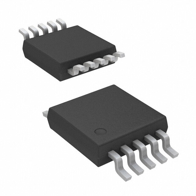
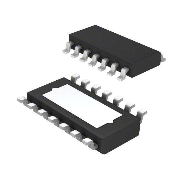
| 供应商器件封装 | 16-QFN(4x4) |
| 其它名称 | 296-34788-6 |
| 包装 | Digi-Reel® |
| 同步整流器 | 是 |
| 商标 | Texas Instruments |
| 安装类型 | 表面贴装 |
| 安装风格 | SMD/SMT |
| 封装 | Reel |
| 封装/外壳 | 16-VQFN 裸露焊盘 |
| 封装/箱体 | VQFN-16 |
| 工作温度 | -40°C ~ 85°C |
| 工作温度范围 | - 40 C to + 85 C |
| 工厂包装数量 | 250 |
| 开关频率 | 650 kHz |
| 拓扑结构 | Buck |
| 最大工作温度 | + 85 C |
| 最大输入电压 | 18 V |
| 最小工作温度 | - 40 C |
| 标准包装 | 1 |
| 电压-输入 | 4.5 V ~ 18 V |
| 电压-输出 | 0.76 V ~ 5.5 V |
| 电流-输出 | 5.5A |
| 类型 | 降压(降压) |
| 系列 | TPS54526 |
| 设计资源 | http://www.digikey.com/product-highlights/cn/zh/texas-instruments-webench-design-center/3176 |
| 输出数 | 1 |
| 输出电压 | 760 mV to 5.5 V |
| 输出电流 | 5 mA |
| 输出端数量 | 1 Output |
| 输出类型 | 可调式 |
| 配用 | /product-detail/zh/TPS54526EVM-608/TPS54526EVM-608-ND/3588802 |
| 频率-开关 | 650kHz |


- 商务部:美国ITC正式对集成电路等产品启动337调查
- 曝三星4nm工艺存在良率问题 高通将骁龙8 Gen1或转产台积电
- 太阳诱电将投资9.5亿元在常州建新厂生产MLCC 预计2023年完工
- 英特尔发布欧洲新工厂建设计划 深化IDM 2.0 战略
- 台积电先进制程称霸业界 有大客户加持明年业绩稳了
- 达到5530亿美元!SIA预计今年全球半导体销售额将创下新高
- 英特尔拟将自动驾驶子公司Mobileye上市 估值或超500亿美元
- 三星加码芯片和SET,合并消费电子和移动部门,撤换高东真等 CEO
- 三星电子宣布重大人事变动 还合并消费电子和移动部门
- 海关总署:前11个月进口集成电路产品价值2.52万亿元 增长14.8%


PDF Datasheet 数据手册内容提取
Product Sample & Technical Tools & Support & Folder Buy Documents Software Community TPS54526 SLVSB84C–MAY2012–REVISEDJUNE2014 TPS54526 4.5-V to 18-V Input, 5.5-A Synchronous Step-Down Converter with Eco-mode™ 1 Features 3 Description • D-CAP2™ModeEnablesFastTransient The TPS54526 is an adaptive on-time D-CAP2™ 1 mode synchronous buck converter. The TPS54526 Response enables system designers to complete the suite of • LowOutputRippleandAllowsCeramicOutput various end equipment’s power bus regulators with a Capacitor cost effective, low component count, low standby • WideV InputVoltageRange:4.5Vto18V current solution. The main control loop for the IN TPS54526 uses the D-CAP2™ mode control which • OutputVoltageRange:0.76Vto5.5V provides a very fast transient response with no • HighlyEfficientIntegratedFET’sOptimized externalcompensationcomponents.Theadaptiveon- forLowerDutyCycleApplications time control supports seamless transition between –63mΩ(HighSide)and33mΩ (LowSide) PWM mode at higher load conditions and Eco- • HighEfficiency,lessthan10μAatshutdown mode™ operation at light loads. Eco-mode™ allows the TPS54526 to maintain high efficiency during • HighInitialBandgapReferenceAccuracy lighter load conditions. The TPS54526 also has a • AdjustableSoftStart proprietary circuit that enables the device to adopt to • Pre-BiasedSoftStart both low equivalent series resistance (ESR) output • 650-kHzSwitchingFrequency(f ) capacitors, such as POSCAP, SP-CAP, and ultra-low SW ESR ceramic capacitors. The device operates from • CycleByCycleOverCurrentLimit 4.5-V to 18-V VIN input. The output voltage can be • PowerGoodOutput programmed between 0.76V and 5.5V. The device • Auto-SkipEco-mode™forHighEfficiencyatLight also features an adjustable soft start time and a Load power good function. The TPS54526 is available in the 14-pin HTSSOP package and the 16 pin QFN 2 Applications package,designedtooperatefrom –40°Cto85°C. • WideRangeofApplicationsforLowVoltage DeviceInformation(1) System PARTNUMBER PACKAGE BODYSIZE(NOM) – DigitalTVPowerSupply HTSSOP(14) 5.00mmx4.40mm TPS54526 – HighDefinitionBlu-rayDisc™Players VQFN(16) 4.00mmx4.00mm – NetworkingHomeTerminal (1) For all available packages, see the orderable addendum at – DigitalSetTopBox(STB) theendofthedatasheet. 4 Simplified Schematic U1 VO(50 mV/div ac coupled) TPS54526PWP I (2A/div) OUT Slew Rate (0.35A/µsec) Time Scale (100µsec/div) 1 An IMPORTANT NOTICE at the end of this data sheet addresses availability, warranty, changes, use in safety-critical applications, intellectualpropertymattersandotherimportantdisclaimers.PRODUCTIONDATA.
TPS54526 SLVSB84C–MAY2012–REVISEDJUNE2014 www.ti.com Table of Contents 1 Features.................................................................. 1 8.2 FunctionalBlockDiagram.........................................8 2 Applications........................................................... 1 8.3 FeatureDescription...................................................9 3 Description............................................................. 1 8.4 DeviceFunctionalModes........................................11 4 SimplifiedSchematic............................................. 1 9 ApplicationandImplementation........................ 12 9.1 ApplicationInformation............................................12 5 RevisionHistory..................................................... 2 9.2 TypicalApplication .................................................12 6 PinConfigurationandFunctions......................... 3 10 PowerSupplyRecommendations..................... 17 7 Specifications......................................................... 4 11 Layout................................................................... 17 7.1 AbsoluteMaximumRatings......................................4 11.1 LayoutGuidelines.................................................17 7.2 HandlingRatings......................................................4 11.2 LayoutExample....................................................18 7.3 RecommendedOperatingConditions.......................4 12 DeviceandDocumentationSupport................. 20 7.4 ThermalInformation..................................................5 7.5 ElectricalCharacteristics...........................................5 12.1 Trademarks...........................................................20 7.6 TimingRequirements................................................6 12.2 ElectrostaticDischargeCaution............................20 7.7 TypicalCharacteristics..............................................7 12.3 Glossary................................................................20 8 DetailedDescription.............................................. 8 13 Mechanical,Packaging,andOrderable Information........................................................... 20 8.1 Overview...................................................................8 13.1 ThermalInformation..............................................20 5 Revision History NOTE:Pagenumbersforpreviousrevisionsmaydifferfrompagenumbersinthecurrentversion. ChangesfromRevisionB(January2014)toRevisionC Page • ChangedthedatasheettothenewTIstandardformat ........................................................................................................ 1 • AddedtheHandlingRatingstable.......................................................................................................................................... 4 • AddedtheTimingRequirementstable................................................................................................................................... 6 • AddedthePowerSupplyRecommendationssection.......................................................................................................... 17 ChangesfromRevisionA(July2013)toRevisionB Page • ChangethedatasheetTitleFrom:4.5-Vto18-VInput,5.5-ASynchronousStep-DownConverterwithEco-mode™ To:4.5-Vto18-VInput,3-ASynchronousStep-DownConverterwithEco-mode™............................................................. 1 ChangesfromOriginal(May2012)toRevisionA Page • ChangedtheOver/UnderVoltageProtectionsection.From:"asthehigh-sideMOSFETdriverturnsoffandthelow- sideMOSFETturnson"To:"asboththehigh-sideandlow-sideMOSFETdriversturnoff"............................................... 10 2 SubmitDocumentationFeedback Copyright©2012–2014,TexasInstrumentsIncorporated ProductFolderLinks:TPS54526
TPS54526 www.ti.com SLVSB84C–MAY2012–REVISEDJUNE2014 6 Pin Configuration and Functions RSAPACKAGE PWPPACKAGE (TOPVIEW) (TOPVIEW) 3 2 1 O N N N V VI VI VI VO 1 14 VIN2 16 15 14 13 VFB 2 13 VIN1 VFB 1 12 VBST VREG5 3 12 VBST VREG5 2 11 SW3 POWER PAD SS 4 POWER PAD 11 SW2 SS 3 10 SW2 GND 4 9 SW1 GND 5 10 SW1 5 6 7 8 PG 6 9 PGND2 PG EN D1 D2 N N G G P P EN 7 8 PGND1 PinFunctions PIN DESCRIPTION NAME NUMBER PWP14 RSA16 VO 1 16 Connecttooutputofconverter.Thispinisusedforoutputdischargefunction. VFB 2 1 Converterfeedbackinput.Connecttooutputvoltagewithfeedbackresistordivider. 5.5Vpowersupplyoutput.Acapacitor(typical1µF)shouldbeconnectedtoGND.VREG5isnot VREG5 3 2 activewhenENislow. SS 4 3 Soft-startcontrol.AnexternalcapacitorshouldbeconnectedtoGND. GND 5 4 Signalgroundpin. PG 6 5 Opendrainpowergoodoutput. EN 7 6 Enablecontrolinput.ENisactivehighandmustbepulleduptoenablethedevice. PGND1, Groundreturnsforlow-sideMOSFET.Alsoserveasinputsofcurrentcomparators.Connect 8,9 7,8 PGND2 PGNDandGNDstronglytogetherneartheIC. SW1,SW2, Switchnodeconnectionbetweenhigh-sideNFETandlow-sideNFET.Alsoserveasinputsto SW3(1) 10,11 9,10,11 currentcomparators. Supplyinputforhigh-sideNFETgatedriver(boostterminal).Connectcapacitorfromthispinto VBST 12 12 respectiveSW1,SW2terminals.AninternalPNdiodeisconnectedbetweenVREG5toVBSTpin. VIN1,VIN2, PowerinputandconnectedtohighsideNFETdrain.Supplyinputfor5-Vinternallinearregulator VIN3(1) 13,14 13,14,15 forthecontrolcircuitry. Thermalpadofthepackage.Mustbesolderedtoachieveappropriatedissipation.Shouldbe PowerPAD™ Backside Backside connectedtoPGND. (1) SW3,VIN3appliesto16pinpackageonly. Copyright©2012–2014,TexasInstrumentsIncorporated SubmitDocumentationFeedback 3 ProductFolderLinks:TPS54526
TPS54526 SLVSB84C–MAY2012–REVISEDJUNE2014 www.ti.com 7 Specifications 7.1 Absolute Maximum Ratings overoperatingfree-airtemperaturerange(unlessotherwisenoted) (1) MIN MAX UNIT VIN1,VIN2,EN –0.3 20 V VBST –0.3 26 V VBST(10nstransient) –0.3 28 V Inputvoltagerange VBST(vsSw1,SW2) –0.3 6.5 V VFB,VO,SS,PG –0.3 6.5 V SW1,SW2 –2 20 V SW1,SW2(10nstransient) –3 22 V VREG5 –0.3 6.5 V Outputvoltagerange PGND1,PGND2 –0.3 0.3 V VoltagefromGNDtoPowerPAD™,V –0.2 0.2 V diff Operatingjunctiontemperature,T –40 150 °C J (1) Stressesbeyondthoselistedunderabsolutemaximumratingsmaycausepermanentdamagetothedevice.Thesearestressratings only,andfunctionaloperationofthedeviceattheseoranyotherconditionsbeyondthoseindicatedunderrecommendedoperating conditionsisnotimplied.Exposuretoabsolute-maximum-ratedconditionsforextendedperiodsmayaffectdevicereliability. 7.2 Handling Ratings MIN MAX UNIT T Storagetemperaturerange –55 150 °C stg Humanbodymodel(HBM),perANSI/ESDA/JEDECJS-001,all pins(1) –2 2 kV V Electrostaticdischarge (ESD) Chargeddevicemodel(CDM),perJEDECspecification JESD22-C101,allpins(2) –500 500 V (1) JEDECdocumentJEP155statesthat500-VHBMallowssafemanufacturingwithastandardESDcontrolprocess. (2) JEDECdocumentJEP157statesthat250-VCDMallowssafemanufacturingwithastandardESDcontrolprocess. 7.3 Recommended Operating Conditions overoperatingfree-airtemperaturerange(unlessotherwisenoted) MIN MAX UNIT V Supplyinputvoltagerange 4.5 18 V IN VBST –0.3 24 VBST(10nstransient) –0.3 27 VBST(vsSw1,SW2) –0.3 5.7 SS,PG –0.3 5.7 V Inputvoltagerange EN –0.3 18 V I VO,VFB –0.3 5.5 SW1,SW2 –1.8 18 SW1,SW2(10nstransient) –3 21 PGND1,PGND2 –0.3 0.1 V Outputvoltagerange VREG5 –0.3 5.7 V O I OutputCurrentrange I 0 5 mA O VREG5 T Operatingfree-airtemperature –40 85 °C A T Operatingjunctiontemperature –40 150 °C J 4 SubmitDocumentationFeedback Copyright©2012–2014,TexasInstrumentsIncorporated ProductFolderLinks:TPS54526
TPS54526 www.ti.com SLVSB84C–MAY2012–REVISEDJUNE2014 7.4 Thermal Information TPS54526 THERMALMETRIC(1) UNITS PWP(14)PINS RSA(16)PINS R Junction-to-ambientthermalresistance 43.7 35.2 θJA R Junction-to-case(top)thermalresistance 33.1 40.6 θJCtop R Junction-to-boardthermalresistance 28.4 12.3 θJB °C/W ψ Junction-to-topcharacterizationparameter 1.3 0.8 JT ψ Junction-to-boardcharacterizationparameter 28.2 12.4 JB R Junction-to-case(bottom)thermalresistance 4.7 3.6 θJCbot (1) Formoreinformationabouttraditionalandnewthermalmetrics,seetheICPackageThermalMetricsapplicationreport,SPRA953. 7.5 Electrical Characteristics overoperatingfree-airtemperaturerange,V =12V(unlessotherwisenoted) IN PARAMETER TESTCONDITIONS MIN TYP MAX UNIT SUPPLYCURRENT V current,T =25°C,EN=5V, I Operating-non-switchingsupplycurrent IN A 900 1400 μA VIN V =0.8V VFB I Shutdownsupplycurrent V current,T =25°C,EN=0V 3.6 10 μA VINSDN IN A LOGICTHRESHOLD V ENhigh-levelinputvoltage 1.6 V ENH V ENlow-levelinputvoltage 0.6 V ENL R ENpinresistancetoGND V =12V 220 440 880 kΩ EN EN VFBVOLTAGEANDDISCHARGERESISTANCE VFBvoltagelightloadmode,T =25°C, A 771 V =1.05V,I =10mA O O T =25°C,V =1.05V,continuousmode 757 765 773 A O VFBTH VFBthresholdvoltage TmAod=e0(°1C) to85°C,VO=1.05V,continuous 753 777 mV T =–40°Cto85°C,V =1.05V,continuous mAode(1) O 751 779 I VFBinputcurrent V =0.8V,T =25°C 0 ±0.15 μA VFB VFB A R V dischargeresistance V =0V,V =0.5V,T =25°C 50 100 Ω Dischg O EN O A VREG5OUTPUT T =25°C,6V<V <18V, V VREG5outputvoltage A IN 5.2 5.5 5.7 V VREG5 0<I <5mA VREG5 V VREG5Lineregulation 6.0V<V <18V,I =5mA 20 mV VREG5 IN VREG5 V VREG5Loadregulation 0mA<I <5mA 100 mV VREG5 VREG5 I VREG5Outputcurrent V =6V,V =4V,T =25°C 60 mA VREG5 IN VREG5 A MOSFET R Highsideswitchresistance T =25°C,V -V =5.5V 63 mΩ dsonh A BST SW1,2 R Lowsideswitchresistance T =25°C 33 mΩ dsonl A (1) Notproductiontested. Copyright©2012–2014,TexasInstrumentsIncorporated SubmitDocumentationFeedback 5 ProductFolderLinks:TPS54526
TPS54526 SLVSB84C–MAY2012–REVISEDJUNE2014 www.ti.com Electrical Characteristics (continued) overoperatingfree-airtemperaturerange,V =12V(unlessotherwisenoted) IN PARAMETER TESTCONDITIONS MIN TYP MAX UNIT CURRENTLIMIT I Currentlimit L =1.5μH(2), 6.1 6.9 8.4 A ocl OUT THERMALSHUTDOWN Shutdowntemperature (2) 165 T Thermalshutdownthreshold °C SDN Hysteresis (2) 35 SOFTSTART I SSchargecurrent V =1.0V 4.2 6.0 7.8 μA SSC SS I SSdischargecurrent V =0.5V 0.1 0.2 mA SSD SS POWERGOOD V rising(good) 85 90 95 % VFB V PGthreshold THPG V falling(fault) 85 % VFB I PGsinkcurrent V =0.5V 2.5 5 mA PG PG OUTPUTUNDERVOLTAGEANDOVERVOLTAGEPROTECTION V OutputOVPtripthreshold OVPdetect 120 125 130 % OVP UVPdetect 60 65 70 % V OutputUVPtripthreshold UVP Hysteresis 10 % UVLO WakeupVREG5voltage 3.31 3.61 3.91 V UVLOthreshold FallVREG5voltage 2.82 3.12 3.42 V UVLO HysteresisVREG5voltage 0.37 0.49 0.61 (2) Notproductiontested. 7.6 Timing Requirements PARAMETER TESTCONDITIONS MIN TYP MAX UNIT ON-TIMETIMERCONTROL t Ontime V =12V,V =1.05V 155 ns ON IN O t Minimumofftime T =25°C,V =0.7V 260 330 ns OFF(MIN) A FB OUTPUTUNDERVOLTAGEANDOVERVOLTAGEPROTECTION t OutputOVPpropdelay 10 μs OVPDEL t OutputUVPdelay 0.25 ms UVPDEL t OutputUVPenabledelay Relativetosoft-starttime x1.7 UVPEN 6 SubmitDocumentationFeedback Copyright©2012–2014,TexasInstrumentsIncorporated ProductFolderLinks:TPS54526
TPS54526 www.ti.com SLVSB84C–MAY2012–REVISEDJUNE2014 7.7 Typical Characteristics V =12V,T =25°C(unlessotherwisenoted) IN A 1200 12 1000 10 A) Supply Current (µA) 468000000 Current−Shutdown Current (µ 468 200 Supply 2 VIN = 12 V VIN = 12 V 0 0 −50 0 50 100 150 −50 0 50 100 150 Junction Temperature (°C) Junction Temperature (°C) G006 G005 Figure1.V CurrentvsJunctionTemperature Figure2.V ShutdownCurrentvsJunctionTemperature IN IN 50 800 45 40 700 ut Current (µA) 233505 Frequency (kHz) 600 N Inp 20 hing E 15 witc S 500 10 5 VOUT = 1.05 V 0 VIN = 12 V VVOOUUTT == 13..83 VV 0 5 10 15 20 400 EN Input Voltage (V) 0 5 10 15 20 Input Voltage (V) G002 G004 I =1A O Figure3.ENCurrentvsENVoltage Figure4.SwitchingFrequencyvsInputVoltage 900 6 800 5 700 Hz) 600 4 witching Frequency (k 345000000 Output Current (A) 23 S 200 1 100 VVOOUUTT == 11..085 V V VVOOUUTT == 15..00 −V 4.5 V VOUT = 3.3 V VIN = 12 V VOUT = 5.5 V 0 0 0.01 0.1 1 10 −50 −25 0 25 50 75 100 Output Current (A) Ambient Temperature (°C) G007 G008 Figure5.SwitchingFrequencyvsOutputCurrent Figure6.OutputCurrentvsAmbientTemperature Copyright©2012–2014,TexasInstrumentsIncorporated SubmitDocumentationFeedback 7 ProductFolderLinks:TPS54526
TPS54526 SLVSB84C–MAY2012–REVISEDJUNE2014 www.ti.com 8 Detailed Description 8.1 Overview The TPS54526 is a 5.5-A synchronous step-down (buck) converter with two integrated N-channel MOSFETs and auto-skip Eco-mode™ to improve light lode efficiency. It operates using D-CAP2™ mode control. The fast transient response of D-CAP2™ control reduces the output capacitance required to meet a specific level of performance. Proprietary internal circuitry allows the use of low ESR output capacitors including ceramic and specialpolymertypes. 8.2 Functional Block Diagram -35% UV VIN2 VIN 14 OV 13VIN1 1 VO +25% VREG5 VBST 12 Control logic Ref SS 1shot 2 11 SW2 VO VFB XCON SW1 10 SGND VREG5 VREG5 Ceramic 3 Capacitor 1mF SS 4 9 PGND2 PGND1 Softstart SW 8 PGND SS ZC PGND 5 GND SW OCP SGND Ref VIN PGND 6 PG -10% UV VREG5 OV Protection UVLO UVLO Logic EN EN 7 TSD Logic REF Ref A. TheblockdiagramshownisforthePWP14pinpackage.TheQFN16pinpackageblockdiagramisidenticalexcept forthepinout. 8 SubmitDocumentationFeedback Copyright©2012–2014,TexasInstrumentsIncorporated ProductFolderLinks:TPS54526
TPS54526 www.ti.com SLVSB84C–MAY2012–REVISEDJUNE2014 8.3 Feature Description 8.3.1 PWMOperation The main control loop of the TPS54526 is an adaptive on-time pulse width modulation (PWM) controller that supports a proprietary D-CAP2™ mode control. D-CAP2™ mode control combines constant on-time control with an internal compensation circuit for pseudo-fixed frequency and low external component count configuration with bothlowESRandceramicoutputcapacitors.Itisstablewithvirtuallynorippleattheoutput. At the beginning of each cycle, the high-side MOSFET is turned on. The MOSFET is turned off after the internal one-shot timer expires. The one-shot timer is set by the converter input voltage, VIN, and the output voltage, VO, to maintain a pseudo-fixed frequency over the input voltage range, hence it is called adaptive on-time control. The one-shot timer is reset and the high-side MOSFET is turned on again when the feedback voltage falls below the reference voltage. An internal ramp is added to reference voltage to simulate output ripple, eliminating the needforESRinducedoutputripplefromD-CAP2™modecontrol. 8.3.2 PWMFrequencyandAdaptiveOn-TimeControl TPS54526 uses an adaptive on-time control scheme and does not have a dedicated on board oscillator. The TPS54526 runs with a pseudo-constant frequency of 650 kHz by using the input voltage and output voltage to set the on-time one-shot timer. The on-time is inversely proportional to the input voltage and proportional to the outputvoltage,therefore,whenthedutyratioisVOUT/VIN,thefrequencyisconstant. 8.3.3 SoftStartandPre-BiasedSoftStart The soft start function is adjustable. When the EN pin becomes high, 6 μA current begins charging the capacitor which is connected from the SS pin to GND. Smooth control of the output voltage is maintained during start up. The equation for the slow start time is shown in Equation 1. VFB voltage is 0.765 V and SS pin source current is 6μA. C (nF)xV ´1.1 C (nF)x0.765´1.1 SS REF SS t (ms)= = SS I (mA) 6 SS (1) The TPS54526 contains a unique circuit to prevent current from being pulled from the output during startup if the output is pre-biased. When the soft-start commands a voltage higher than the pre-bias level (internal soft start becomes greater than feedback voltage V ), the controller slowly activates synchronous rectification by starting FB the first low side FET gate driver pulses with a narrow on-time. It then increments that on-time on a cycle-by- cycle basis until it coincides with the time dictated by (1-D), where D is the duty cycle of the converter. This scheme prevents the initial sinking of the pre-bias output, and ensure that the out voltage (VO) starts and ramps up smoothly into regulation and the control loop is given time to transition from pre-biased start-up to normal modeoperation. 8.3.4 PowerGood The TPS54526 has power-good open drain output. The power good function is activated after soft start has finished. The power good function becomes active after 1.7 times soft-start time. When the output voltage is within -10% of the target value, internal comparators detect power good state and the power good signal becomeshigh.Rpgresistervalue,whichisconnectedbetweenPGandVREG5,isrequiredfrom25kΩto150kΩ. If the feedback voltage goes under 15% of the target value, the power good signal becomes low after a 5 μs internaldelay. 8.3.5 VREG5 VREG5 is an internally generated voltage source used by the TPS54526. It is derived directly from the input voltage and is nominally regulated to 5.5 V when the input voltage is above 5.6 V. The output of the VREG5 regulator is the input to the internal UVLO function. VREG5 must be above the UVLO wake up threshold voltage (3.6 V typical) for the TPS54526 to function. Connect a 1 µF capacitor between pin 3 of the TPS54526 and power ground for proper regulation of the VREG5 output. The VREG5 output voltage is available for external use. It is recommended to use no more than 5 mA for external loads. The VREG5 output is disabled when the TPS54526ENpinisopenorpulledlow. Copyright©2012–2014,TexasInstrumentsIncorporated SubmitDocumentationFeedback 9 ProductFolderLinks:TPS54526
TPS54526 SLVSB84C–MAY2012–REVISEDJUNE2014 www.ti.com Feature Description (continued) 8.3.6 OutputDischargeControl TPS54526 discharges the output when EN is low, or the controller is turned off by the protection functions (OVP, UVP, UVLO and thermal shutdown). The output is discharged by an internal 50-Ω MOSFET which is connected from VO to PGND. The internal low-side MOSFET is not turned on during the output discharge operation to avoidthepossibilityofcausingnegativevoltageattheoutput. 8.3.7 CurrentProtection The output overcurrent protection (OCP) is implemented using a cycle-by-cycle valley detect control circuit. The switch current is monitored by measuring the low-side FET switch voltage between the SW pin and GND. This voltage is proportional to the switch current. To improve accuracy, the voltage sensing is temperature compensated. During the on-time of the high-side FET switch, the switch current increases at a linear rate determined by V , IN V , the on-time, and the output inductor value. During the on-time of the low-side FET switch, this current OUT decreases linearly. The average value of the switch current is the load current I . If the measured voltage is OUT above the voltage proportional to the current limit. Then, the device constantly monitors the low-side FET switch voltage,whichisproportionaltotheswitchcurrent,duringthelow-sideon-time. The converter maintains the low-side switch on until the measured voltage is below the voltage corresponding to the current limit at which time the switching cycle is terminated and a new switching cycle begins. In subsequent switchingcycles,theon-timeissettoafixedvalueandthecurrentismonitoredinthesamemanner. There are some important considerations for this type of overcurrent protection. The load current one half of the peak-to-peak inductor current higher than the overcurrent threshold. Also when the current is being limited, the output voltage tends to fall as the demanded load current may be higher than the current available from the converter. This may cause the output under-voltage protection circuit to be activated. When the overcurrent conditionisremoved,theoutputvoltagewillreturntotheregulatedvalue.Thisprotectionisnon-latching. 8.3.8 Over/UnderVoltageProtection TPS54526 monitors a resistor divided feedback voltage to detect over and under voltage. When the feedback voltage becomes higher than 125% of the target voltage, the OVP comparator output goes high and the circuit latchesasboththehigh-sideandlow-sideMOSFETdriversturnsoff.Whenthefeedbackvoltagebecomeslower than 65% of the target voltage, the UVP comparator output goes high and an internal UVP delay counter begins. After 250 μs, the device latches off both internal top and bottom MOSFET. This function is enabled approximately1.7xsoftstarttime. 8.3.9 UVLOProtection Undervoltage lock out protection (UVLO) monitors the voltage of the V pin. When the V voltage is lower REG5 REG5 thanUVLOthresholdvoltage,theTPS54526isshutoff.Thisisprotectionisnon-latching. 8.3.10 ThermalShutdown TPS54526 monitors the temperature of itself. If the temperature exceeds the threshold value (typically 165°C), thedeviceisshutoff.Thisisnon-latchprotection. 10 SubmitDocumentationFeedback Copyright©2012–2014,TexasInstrumentsIncorporated ProductFolderLinks:TPS54526
TPS54526 www.ti.com SLVSB84C–MAY2012–REVISEDJUNE2014 8.4 Device Functional Modes 8.4.1 Auto-SkipEco-Mode™Control The TPS54526 is designed with Auto-Skip Eco-mode™ to increase light load efficiency. As the output current decreases from heavy load condition, the inductor current is also reduced and eventually comes to point that its rippled valley touches zero level, which is the boundary between continuous conduction and discontinuous conduction modes. The rectifying MOSFET is turned off when its zero inductor current is detected. As the load current further decreases the converter run into discontinuous conduction mode. The on-time is kept almost the same as it was in the continuous conduction mode so that it takes longer time to discharge the output capacitor with smaller load current to the level of the reference voltage. The transition point to the light load operation I currentcanbecalculatedinEquation2. OUT(LL) 1 (V -V )×V I = × IN OUT OUT OUT(LL) 2×L×f V SW IN (2) Copyright©2012–2014,TexasInstrumentsIncorporated SubmitDocumentationFeedback 11 ProductFolderLinks:TPS54526
TPS54526 SLVSB84C–MAY2012–REVISEDJUNE2014 www.ti.com 9 Application and Implementation 9.1 Application Information 9.2 Typical Application The TPS54526 is an adaptive on-time D-CAP2™ mode synchronous buck converter. Idea applications are: Digital TV Power Supply, High Definition Blu-ray Disc™ Player, Networking Home Terminal and Digital Set Top Box. U1 TPS54526PWP Figure7. SchematicDiagramforThisDesignExample 9.2.1 DesignRequirements Forthisdesignexample,usethefollowinginputparameters. Table1.DesignParameters DESIGNPARAMETERS VALUES Inputvoltagerange 4.5V–18V Outputvoltage 1.05V Outputcurrentrating 0–5.5A Outputvoltageripple 7mV (12V /5.5A) PP IN 9.2.2 DetailedDesignProcedure 9.2.2.1 StepByStepDesignProcedure Tobeginthedesignprocess,thedesignermustknowathefollowingapplicationparameters: • Inputvoltagerange • Outputvoltage • Outputcurrent • Outputvoltageripple • Inputvoltageripple 12 SubmitDocumentationFeedback Copyright©2012–2014,TexasInstrumentsIncorporated ProductFolderLinks:TPS54526
TPS54526 www.ti.com SLVSB84C–MAY2012–REVISEDJUNE2014 9.2.2.2 OutputVoltageResistorsSelection The output voltage is set with a resistor divider from the output node to the VFB pin. It is recommended to use 1%toleranceorbetterdividerresistors.StartbyusingEquation3 tocalculateV OUT To improve efficiency at very light loads consider using larger value resistors, too high of resistance will be more susceptibletonoiseandvoltageerrorsfromtheVFBinputcurrentwillbemorenoticeable ( R1) VOUT=0.765 • 1 + −R2 (3) 9.2.2.3 OutputFilterSelection TheoutputfilterusedwiththeTPS54526isanLCcircuit.ThisLCfilterhasdoublepoleat: 1 F = P 2p L ´C OUT OUT (4) At low frequencies, the overall loop gain is set by the output set-point resistor divider network and the internal gain of the TPS54526. The low frequency phase is 180 degrees. At the output filter pole frequency, the gain rolls off at a -40 dB per decade rate and the phase drops rapidly. D-CAP2™ introduces a high frequency zero that reduces the gain roll off to –20 dB per decade and increases the phase to 90 degrees one decade above the zero frequency. The inductor and capacitor selected for the output filter must be selected so that the double pole of Equation 4 is located below the high frequency zero but close enough that the phase boost provided be the high frequency zero provides adequate phase margin for a stable circuit. To meet this requirement use the valuesrecommendedinTable2 Table2.RecommendedComponentValues OutputVoltage(V) R1(kΩ) R2(kΩ) C4(pF)(1) L1(µH) C8+C9(µF) 1 6.81 22.1 1.0-1.5 22-68 1.05 8.25 22.1 1.0-1.5 22-68 1.2 12.7 22.1 1.0-1.5 22-68 1.5 21.5 22.1 1.5 22-68 1.8 30.1 22.1 5-22 1.5 22-68 2.5 49.9 22.1 5-22 2.2 22-68 3.3 73.2 22.1 5-22 2.2 22-68 5 124 22.1 5-22 3.3 22-68 (1) Optional For higher output voltages at or above 1.8 V, additional phase boost can be achieved by adding a feed forward capacitor(C4)inparallelwithR1. Since the DC gain is dependent on the output voltage, the required inductor value increases as the output voltage increases. For higher output voltages above 1.8 V, additional phase boost can be achieved by adding a feedforwardcapacitor(C4)inparallelwithR1 The inductor peak-to-peak ripple current, peak current and RMS current are calculated using Equation 5, Equation 6 and Equation 7. The inductor saturation current rating must be greater than the calculated peak current and the RMS or heating current rating must be greater than the calculated RMS current. Use 650 kHz for f . SW V V - V Ilp - p = OUT • IN (max) OUT V L •f IN (max) O SW (5) Ilp - p I = I + lpeak O 2 (6) − √ 1 I = I 2+ −Ilp - p2 Lo(RMS) O 12 (7) Copyright©2012–2014,TexasInstrumentsIncorporated SubmitDocumentationFeedback 13 ProductFolderLinks:TPS54526
TPS54526 SLVSB84C–MAY2012–REVISEDJUNE2014 www.ti.com For this design example, the calculated peak current is 6.01 A and the calculated RMS current is 5.5 A. The inductor used is a TDK SPM6530-1R5M100 with a peak current rating of 11.5 A and an RMS current rating of11A. The capacitor value and ESR determines the amount of output voltage ripple. The TPS54526 is intended for use with ceramic or other low ESR capacitors. Recommended values range from 22uF to 68uF. Use Equation 8 to determinetherequiredRMScurrentratingfortheoutputcapacitor V • (V - V ) I =−−OUT IN OUT CO(RMS) √12 •V •L •f IN O SW (8) For this design two TDK C3216X5R0J226M 22uF output capacitors are used. The typical ESR is 2 mΩ each. ThecalculatedRMScurrentis.284Aandeachoutputcapacitorisratedfor4A. 9.2.2.4 InputCapacitorSelection The TPS54526 requires an input decoupling capacitor and a bulk capacitor is needed depending on the application. A ceramic capacitor over 10 uF. is recommended for the decoupling capacitor. An additional 0.1 µF capacitor from pin 14 to ground is recommended to improve the stability of the over-current limit function. The capacitorvoltageratingneedstobegreaterthanthemaximuminputvoltage. 9.2.2.5 BootstrapCapacitorSelection A 0.1 μF ceramic capacitor must be connected between the VBST to SW pin for proper operation. It is recommendedtouseaceramiccapacitor. 9.2.2.6 VREG5CapacitorSelection A 1.0 μF ceramic capacitor must be connected between the VREG5 to GND pin for proper operation. It is recommendedtouseaceramiccapacitor. 14 SubmitDocumentationFeedback Copyright©2012–2014,TexasInstrumentsIncorporated ProductFolderLinks:TPS54526
TPS54526 www.ti.com SLVSB84C–MAY2012–REVISEDJUNE2014 9.2.3 ApplicationCurve 1.09 1.10 VO = 1.05 V 1.09 1.08 1.08 1.07 1.07 V) V) e ( e ( 1.06 g g a a olt 1.06 olt 1.05 V V ut ut utp utp 1.04 O O 1.05 1.03 1.02 1.04 VIN = 5 V VIN = 12 V 1.01 IO = 10 mA VIN = 18 V IO = 1 A 1.03 1.00 0.0 0.5 1.0 1.5 2.0 2.5 3.0 3.5 4.0 4.5 5.0 5.5 0 5 10 15 20 Output Current (A) Input Voltage (V) G007 G007 Figure8.1.05VOutputVoltagevsOutputCurrent Figure9.1.05VOutputVoltagevsInputVoltage 100 100 90 90 80 80 70 70 %) 60 %) 60 ncy ( 50 ncy ( 50 e e Effici 40 Effici 40 30 30 20 20 VOUT = 1.8 V VOUT = 1.8 V 10 VOUT = 2.5 V 10 VOUT = 2.5 V VOUT = 3.3 V VOUT = 3.3 V 0 0 0.0 0.5 1.0 1.5 2.0 2.5 3.0 3.5 4.0 4.5 5.0 5.5 0.001 0.01 0.1 1 10 Output Current (A) Output Current (A) G000 G001 Figure10.EfficiencyvsOutputCurrent Figure11.LightLoadEfficiencyvsOutputCurrent EN (10 V/div) VO(50 mV/div ac coupled) VREG5 (5 V/div) IOUT(2A/div) VO(500 mV/div) PG (5 V/div) Slew Rate (0.35A/µsec) Time Scale (100µsec/div) 1.05V 50mAto5.5A Figure12.LoadTransientResponse Figure13.StartupWaveform Copyright©2012–2014,TexasInstrumentsIncorporated SubmitDocumentationFeedback 15 ProductFolderLinks:TPS54526
TPS54526 SLVSB84C–MAY2012–REVISEDJUNE2014 www.ti.com VO= 1.05 V VO= 1.05 V VO(10 mV/div ac coupled) IO = 30 mA VO(20 mV/div ac coupled) SW (5 V/div) SW (5 V/div) I =30mA O I =5.5A O Figure15.Eco-modeVoltageRippleatOutput Figure14.VoltageRippleatOutput VO= 1.05 V VIN(50 mV/div ac coupled) SW (5 V/div) I =5.5A O Figure16.VoltageRippleatInput 16 SubmitDocumentationFeedback Copyright©2012–2014,TexasInstrumentsIncorporated ProductFolderLinks:TPS54526
TPS54526 www.ti.com SLVSB84C–MAY2012–REVISEDJUNE2014 10 Power Supply Recommendations The device is designed to operate from an input voltage supply range between 4.5 V and 18 V. This input supply should be well regulated. If the input supply is located more than a few inches from the TPS54526 converter additional bulk capacitance may be required in addition to the ceramic bypass capacitors. An electrolytic capacitorwithavalueof100μFisatypicalchoice. 11 Layout 11.1 Layout Guidelines • Keeptheinputswitchingcurrentloopassmallaspossible. • Keep the SW node as physically small and short as possible to minimize parasitic capacitance and inductance and to minimize radiated emissions. Kelvin connections should be brought from the output to the feedbackpinofthedevice. • Keepanalogandnon-switchingcomponentsawayfromswitchingcomponents. • Makeasinglepointconnectionfromthesignalgroundtopowerground. • Donotallowswitchingcurrenttoflowunderthedevice. • VREG5capacitorshouldbeplacednearthedevice,andconnectedPGND. • OutputcapacitorshouldbeconnectedtoabroadpatternofthePGND. • Voltagefeedbackloopshouldbeasshortaspossible,andpreferablywithgroundshield. • LowerresistorofthevoltagedividerwhichisconnectedtotheVFBpinshouldbetiedtoAGND. • ProvidingsufficientviaispreferableforVIN,SWandPGNDconnection. • PCBpatternforVINandSWshouldbeasbroadaspossible. • VINCapacitorshouldbeplacedasnearaspossibletothedevice. • Thetopsidepowerground(PGND)copperfillareaneartheICshouldbeaslargeaspossible.Thiswillaidin thermaldissipationaswelllowerconductionlossesinthegroundreturn • Exposed pad of device must be connected to PGND with solder. The PGND area under the IC should be as large as possible and completely cover the exposed thermal pad. The bottom side of the board should contain a large copper area under the device that is directly connected to the exposed area with small diameter vias. Small diameter vias will prevent solder from being drawn away from the exposed thermal pad. Any additional internal layers should also contain copper ground areas under the device and be connected to thethermalvias. Copyright©2012–2014,TexasInstrumentsIncorporated SubmitDocumentationFeedback 17 ProductFolderLinks:TPS54526
TPS54526 SLVSB84C–MAY2012–REVISEDJUNE2014 www.ti.com 11.2 Layout Example VIN Additional Thermal VIN Vias VCIUNR ORVEENRT INPUT STABILITY BYPASS CAPACITOR CAPACITOR FEEDBACK VOUT EXPOSED VIN2 RESISTORS POWERPAD AREA VFB VIN1 BOOST VREG5 VBST CAPACITOR VOUT BIAS SS SW1 CAP GND SW2 OUTPUT INDUCTOR OUTPUT PG PGND1 SLOW FILTER START CAPACITOR CAP EN PGND2 Connection to POWER GROUND on internal or ANALOG Additional bottom layer GROUND Thermal TRACE Vias To Enable Control POWER GROUND VIAto Ground Plane Etch on Bottom Layer or Under Component Figure17. PCBLayoutforPWPPackage 18 SubmitDocumentationFeedback Copyright©2012–2014,TexasInstrumentsIncorporated ProductFolderLinks:TPS54526
TPS54526 www.ti.com SLVSB84C–MAY2012–REVISEDJUNE2014 Layout Example (continued) VIN VIAto Ground Plane VIN Etch on Bottom Layer INPUT or Under Component BYPASS CAPACITOR VIN HIGH FREQUENCY BYPASS 3 2 1 CAPACITOR O N N N V VI VI VI POWER GROUND 16 15 14 13 FEEDBACK RESISTORS EXPOSEDTHERMAL VFB 1 PADAREA 12 VBST BOOST CAPACITOR VREG5 2 11 SW3 BIAS CAP SS 3 10 SW2 GND 4 9 SW1 SLOW OUTPUT START 5 6 7 8 INDUCTOR CAP ANALOG G N 1 2 GROUND P E ND ND OUTPUT TRACE G G FILTER P P CAPACITOR VOUT To Enable Control Connection to POWER GROUND on internal or bottom layer Figure18. PCBLayoutforRSAPackage Copyright©2012–2014,TexasInstrumentsIncorporated SubmitDocumentationFeedback 19 ProductFolderLinks:TPS54526
TPS54526 SLVSB84C–MAY2012–REVISEDJUNE2014 www.ti.com 12 Device and Documentation Support 12.1 Trademarks D-CAP2,Eco-modearetrademarksofTexasInstruments. Blu-rayDiscisatrademarkofBlu-rayDiscAssociation. 12.2 Electrostatic Discharge Caution Thesedeviceshavelimitedbuilt-inESDprotection.Theleadsshouldbeshortedtogetherorthedeviceplacedinconductivefoam duringstorageorhandlingtopreventelectrostaticdamagetotheMOSgates. 12.3 Glossary SLYZ022—TIGlossary. Thisglossarylistsandexplainsterms,acronyms,anddefinitions. 13 Mechanical, Packaging, and Orderable Information The following pages include mechanical, packaging, and orderable information. This information is the most current data available for the designated devices. This data is subject to change without notice and revision of thisdocument.Forbrowser-basedversionsofthisdatasheet,refertotheleft-handnavigation. 13.1 Thermal Information This PowerPad™ package incorporates an exposed thermal pad that is designed to be directly to an external heatsink. The thermal pad must be soldered directly to the printed board (PCB). After soldering, the PCB can be used as a heatsink. In addition, through the use of thermal vias, the thermal pad can be attached directly to the appropriate copper plane shown in the electrical schematic for the device, or alternatively, can be attached to a special heatsink structure designed into the PCB. This design optimizes the heat transfer from the integrated circuit(IC). For additional information on the PowerPAD™ package and how to use the advantage of its heat dissipating abilities, refer to Technical Brief, PowerPAD™ Thermally Enhanced Package, Texas Instruments Literature No. SLMA002 andApplicationBrief,PowerPAD™MadeEasy,TexasInstrumentsLiteratureNo.SLMA004. Theexposedthermalpaddimensionsforthispackageareshowninthefollowingillustration. 14 8 Thermal Pad 2.46 ° 1 7 2.31 Figure19. ThermalPadDimensions 20 SubmitDocumentationFeedback Copyright©2012–2014,TexasInstrumentsIncorporated ProductFolderLinks:TPS54526
PACKAGE OPTION ADDENDUM www.ti.com 25-Apr-2014 PACKAGING INFORMATION Orderable Device Status Package Type Package Pins Package Eco Plan Lead/Ball Finish MSL Peak Temp Op Temp (°C) Device Marking Samples (1) Drawing Qty (2) (6) (3) (4/5) TPS54526PWP ACTIVE HTSSOP PWP 14 90 Green (RoHS CU NIPDAU Level-2-260C-1 YEAR -40 to 85 PS54526 & no Sb/Br) TPS54526PWPR ACTIVE HTSSOP PWP 14 2000 Green (RoHS CU NIPDAU Level-2-260C-1 YEAR -40 to 85 PS54526 & no Sb/Br) TPS54526RSAR ACTIVE QFN RSA 16 3000 Green (RoHS CU NIPDAU Level-2-260C-1 YEAR -40 to 85 TPS & no Sb/Br) 54526 TPS54526RSAT ACTIVE QFN RSA 16 250 Green (RoHS CU NIPDAU Level-2-260C-1 YEAR -40 to 85 TPS & no Sb/Br) 54526 (1) The marketing status values are defined as follows: ACTIVE: Product device recommended for new designs. LIFEBUY: TI has announced that the device will be discontinued, and a lifetime-buy period is in effect. NRND: Not recommended for new designs. Device is in production to support existing customers, but TI does not recommend using this part in a new design. PREVIEW: Device has been announced but is not in production. Samples may or may not be available. OBSOLETE: TI has discontinued the production of the device. (2) Eco Plan - The planned eco-friendly classification: Pb-Free (RoHS), Pb-Free (RoHS Exempt), or Green (RoHS & no Sb/Br) - please check http://www.ti.com/productcontent for the latest availability information and additional product content details. TBD: The Pb-Free/Green conversion plan has not been defined. Pb-Free (RoHS): TI's terms "Lead-Free" or "Pb-Free" mean semiconductor products that are compatible with the current RoHS requirements for all 6 substances, including the requirement that lead not exceed 0.1% by weight in homogeneous materials. Where designed to be soldered at high temperatures, TI Pb-Free products are suitable for use in specified lead-free processes. Pb-Free (RoHS Exempt): This component has a RoHS exemption for either 1) lead-based flip-chip solder bumps used between the die and package, or 2) lead-based die adhesive used between the die and leadframe. The component is otherwise considered Pb-Free (RoHS compatible) as defined above. Green (RoHS & no Sb/Br): TI defines "Green" to mean Pb-Free (RoHS compatible), and free of Bromine (Br) and Antimony (Sb) based flame retardants (Br or Sb do not exceed 0.1% by weight in homogeneous material) (3) MSL, Peak Temp. - The Moisture Sensitivity Level rating according to the JEDEC industry standard classifications, and peak solder temperature. (4) There may be additional marking, which relates to the logo, the lot trace code information, or the environmental category on the device. (5) Multiple Device Markings will be inside parentheses. Only one Device Marking contained in parentheses and separated by a "~" will appear on a device. If a line is indented then it is a continuation of the previous line and the two combined represent the entire Device Marking for that device. (6) Lead/Ball Finish - Orderable Devices may have multiple material finish options. Finish options are separated by a vertical ruled line. Lead/Ball Finish values may wrap to two lines if the finish value exceeds the maximum column width. Addendum-Page 1
PACKAGE OPTION ADDENDUM www.ti.com 25-Apr-2014 Important Information and Disclaimer:The information provided on this page represents TI's knowledge and belief as of the date that it is provided. TI bases its knowledge and belief on information provided by third parties, and makes no representation or warranty as to the accuracy of such information. Efforts are underway to better integrate information from third parties. TI has taken and continues to take reasonable steps to provide representative and accurate information but may not have conducted destructive testing or chemical analysis on incoming materials and chemicals. TI and TI suppliers consider certain information to be proprietary, and thus CAS numbers and other limited information may not be available for release. In no event shall TI's liability arising out of such information exceed the total purchase price of the TI part(s) at issue in this document sold by TI to Customer on an annual basis. Addendum-Page 2
PACKAGE MATERIALS INFORMATION www.ti.com 15-Jul-2018 TAPE AND REEL INFORMATION *Alldimensionsarenominal Device Package Package Pins SPQ Reel Reel A0 B0 K0 P1 W Pin1 Type Drawing Diameter Width (mm) (mm) (mm) (mm) (mm) Quadrant (mm) W1(mm) TPS54526PWPR HTSSOP PWP 14 2000 330.0 12.4 6.9 5.6 1.6 8.0 12.0 Q1 TPS54526RSAR QFN RSA 16 3000 330.0 12.4 4.25 4.25 1.15 8.0 12.0 Q2 TPS54526RSAT QFN RSA 16 250 180.0 12.4 4.25 4.25 1.15 8.0 12.0 Q2 PackMaterials-Page1
PACKAGE MATERIALS INFORMATION www.ti.com 15-Jul-2018 *Alldimensionsarenominal Device PackageType PackageDrawing Pins SPQ Length(mm) Width(mm) Height(mm) TPS54526PWPR HTSSOP PWP 14 2000 367.0 367.0 35.0 TPS54526RSAR QFN RSA 16 3000 367.0 367.0 35.0 TPS54526RSAT QFN RSA 16 250 210.0 185.0 35.0 PackMaterials-Page2
None
None
None
None
None
None
None
None
IMPORTANTNOTICE TexasInstrumentsIncorporated(TI)reservestherighttomakecorrections,enhancements,improvementsandotherchangestoits semiconductorproductsandservicesperJESD46,latestissue,andtodiscontinueanyproductorserviceperJESD48,latestissue.Buyers shouldobtainthelatestrelevantinformationbeforeplacingordersandshouldverifythatsuchinformationiscurrentandcomplete. TI’spublishedtermsofsaleforsemiconductorproducts(http://www.ti.com/sc/docs/stdterms.htm)applytothesaleofpackagedintegrated circuitproductsthatTIhasqualifiedandreleasedtomarket.AdditionaltermsmayapplytotheuseorsaleofothertypesofTIproductsand services. ReproductionofsignificantportionsofTIinformationinTIdatasheetsispermissibleonlyifreproductioniswithoutalterationandis accompaniedbyallassociatedwarranties,conditions,limitations,andnotices.TIisnotresponsibleorliableforsuchreproduced documentation.Informationofthirdpartiesmaybesubjecttoadditionalrestrictions.ResaleofTIproductsorserviceswithstatements differentfromorbeyondtheparametersstatedbyTIforthatproductorservicevoidsallexpressandanyimpliedwarrantiesforthe associatedTIproductorserviceandisanunfairanddeceptivebusinesspractice.TIisnotresponsibleorliableforanysuchstatements. BuyersandotherswhoaredevelopingsystemsthatincorporateTIproducts(collectively,“Designers”)understandandagreethatDesigners remainresponsibleforusingtheirindependentanalysis,evaluationandjudgmentindesigningtheirapplicationsandthatDesignershave fullandexclusiveresponsibilitytoassurethesafetyofDesigners'applicationsandcomplianceoftheirapplications(andofallTIproducts usedinorforDesigners’applications)withallapplicableregulations,lawsandotherapplicablerequirements.Designerrepresentsthat,with respecttotheirapplications,Designerhasallthenecessaryexpertisetocreateandimplementsafeguardsthat(1)anticipatedangerous consequencesoffailures,(2)monitorfailuresandtheirconsequences,and(3)lessenthelikelihoodoffailuresthatmightcauseharmand takeappropriateactions.DesigneragreesthatpriortousingordistributinganyapplicationsthatincludeTIproducts,Designerwill thoroughlytestsuchapplicationsandthefunctionalityofsuchTIproductsasusedinsuchapplications. TI’sprovisionoftechnical,applicationorotherdesignadvice,qualitycharacterization,reliabilitydataorotherservicesorinformation, including,butnotlimitedto,referencedesignsandmaterialsrelatingtoevaluationmodules,(collectively,“TIResources”)areintendedto assistdesignerswhoaredevelopingapplicationsthatincorporateTIproducts;bydownloading,accessingorusingTIResourcesinany way,Designer(individuallyor,ifDesignerisactingonbehalfofacompany,Designer’scompany)agreestouseanyparticularTIResource solelyforthispurposeandsubjecttothetermsofthisNotice. TI’sprovisionofTIResourcesdoesnotexpandorotherwisealterTI’sapplicablepublishedwarrantiesorwarrantydisclaimersforTI products,andnoadditionalobligationsorliabilitiesarisefromTIprovidingsuchTIResources.TIreservestherighttomakecorrections, enhancements,improvementsandotherchangestoitsTIResources.TIhasnotconductedanytestingotherthanthatspecifically describedinthepublisheddocumentationforaparticularTIResource. Designerisauthorizedtouse,copyandmodifyanyindividualTIResourceonlyinconnectionwiththedevelopmentofapplicationsthat includetheTIproduct(s)identifiedinsuchTIResource.NOOTHERLICENSE,EXPRESSORIMPLIED,BYESTOPPELOROTHERWISE TOANYOTHERTIINTELLECTUALPROPERTYRIGHT,ANDNOLICENSETOANYTECHNOLOGYORINTELLECTUALPROPERTY RIGHTOFTIORANYTHIRDPARTYISGRANTEDHEREIN,includingbutnotlimitedtoanypatentright,copyright,maskworkright,or otherintellectualpropertyrightrelatingtoanycombination,machine,orprocessinwhichTIproductsorservicesareused.Information regardingorreferencingthird-partyproductsorservicesdoesnotconstitutealicensetousesuchproductsorservices,orawarrantyor endorsementthereof.UseofTIResourcesmayrequirealicensefromathirdpartyunderthepatentsorotherintellectualpropertyofthe thirdparty,oralicensefromTIunderthepatentsorotherintellectualpropertyofTI. TIRESOURCESAREPROVIDED“ASIS”ANDWITHALLFAULTS.TIDISCLAIMSALLOTHERWARRANTIESOR REPRESENTATIONS,EXPRESSORIMPLIED,REGARDINGRESOURCESORUSETHEREOF,INCLUDINGBUTNOTLIMITEDTO ACCURACYORCOMPLETENESS,TITLE,ANYEPIDEMICFAILUREWARRANTYANDANYIMPLIEDWARRANTIESOF MERCHANTABILITY,FITNESSFORAPARTICULARPURPOSE,ANDNON-INFRINGEMENTOFANYTHIRDPARTYINTELLECTUAL PROPERTYRIGHTS.TISHALLNOTBELIABLEFORANDSHALLNOTDEFENDORINDEMNIFYDESIGNERAGAINSTANYCLAIM, INCLUDINGBUTNOTLIMITEDTOANYINFRINGEMENTCLAIMTHATRELATESTOORISBASEDONANYCOMBINATIONOF PRODUCTSEVENIFDESCRIBEDINTIRESOURCESOROTHERWISE.INNOEVENTSHALLTIBELIABLEFORANYACTUAL, DIRECT,SPECIAL,COLLATERAL,INDIRECT,PUNITIVE,INCIDENTAL,CONSEQUENTIALOREXEMPLARYDAMAGESIN CONNECTIONWITHORARISINGOUTOFTIRESOURCESORUSETHEREOF,ANDREGARDLESSOFWHETHERTIHASBEEN ADVISEDOFTHEPOSSIBILITYOFSUCHDAMAGES. UnlessTIhasexplicitlydesignatedanindividualproductasmeetingtherequirementsofaparticularindustrystandard(e.g.,ISO/TS16949 andISO26262),TIisnotresponsibleforanyfailuretomeetsuchindustrystandardrequirements. WhereTIspecificallypromotesproductsasfacilitatingfunctionalsafetyorascompliantwithindustryfunctionalsafetystandards,such productsareintendedtohelpenablecustomerstodesignandcreatetheirownapplicationsthatmeetapplicablefunctionalsafetystandards andrequirements.Usingproductsinanapplicationdoesnotbyitselfestablishanysafetyfeaturesintheapplication.Designersmust ensurecompliancewithsafety-relatedrequirementsandstandardsapplicabletotheirapplications.DesignermaynotuseanyTIproductsin life-criticalmedicalequipmentunlessauthorizedofficersofthepartieshaveexecutedaspecialcontractspecificallygoverningsuchuse. Life-criticalmedicalequipmentismedicalequipmentwherefailureofsuchequipmentwouldcauseseriousbodilyinjuryordeath(e.g.,life support,pacemakers,defibrillators,heartpumps,neurostimulators,andimplantables).Suchequipmentincludes,withoutlimitation,all medicaldevicesidentifiedbytheU.S.FoodandDrugAdministrationasClassIIIdevicesandequivalentclassificationsoutsidetheU.S. TImayexpresslydesignatecertainproductsascompletingaparticularqualification(e.g.,Q100,MilitaryGrade,orEnhancedProduct). Designersagreethatithasthenecessaryexpertisetoselecttheproductwiththeappropriatequalificationdesignationfortheirapplications andthatproperproductselectionisatDesigners’ownrisk.Designersaresolelyresponsibleforcompliancewithalllegalandregulatory requirementsinconnectionwithsuchselection. DesignerwillfullyindemnifyTIanditsrepresentativesagainstanydamages,costs,losses,and/orliabilitiesarisingoutofDesigner’snon- compliancewiththetermsandprovisionsofthisNotice. MailingAddress:TexasInstruments,PostOfficeBox655303,Dallas,Texas75265 Copyright©2018,TexasInstrumentsIncorporated