ICGOO在线商城 > 集成电路(IC) > PMIC - 稳压器 - DC DC 开关稳压器 > TPS62042DGQ
 Datasheet下载
- 型号: TPS62042DGQ
- 制造商: Texas Instruments
- 库位|库存: xxxx|xxxx
- 要求:
| 数量阶梯 | 香港交货 | 国内含税 |
| +xxxx | $xxxx | ¥xxxx |
查看当月历史价格
查看今年历史价格
TPS62042DGQ产品简介:
ICGOO电子元器件商城为您提供TPS62042DGQ由Texas Instruments设计生产,在icgoo商城现货销售,并且可以通过原厂、代理商等渠道进行代购。 TPS62042DGQ价格参考¥5.11-¥5.11。Texas InstrumentsTPS62042DGQ封装/规格:PMIC - 稳压器 - DC DC 开关稳压器, 固定 降压 开关稳压器 IC 正 1.5V 1 输出 1.2A 10-TFSOP,10-MSOP(0.118",3.00mm 宽)裸露焊盘。您可以下载TPS62042DGQ参考资料、Datasheet数据手册功能说明书,资料中有TPS62042DGQ 详细功能的应用电路图电压和使用方法及教程。
TPS62042DGQ 是 Texas Instruments(德州仪器)生产的一款高效、低电压输入的 DC-DC 开关稳压器,广泛应用于对效率和空间有较高要求的便携式电子产品中。

该器件的主要应用场景包括:

1. 便携式电子设备:如智能手机、平板电脑、数码相机等,用于将电池电压高效转换为处理器、内存或传感器等模块所需的工作电压。

2. 嵌入式系统与工业控制设备:在需要稳定电源供应的小型控制系统中,TPS62042DGQ 可提供高效率的电压调节,减少发热并延长运行时间。

3. 无线通信模块:如 Wi-Fi、蓝牙或 Zigbee 模块,适用于需低功耗和高效能电源管理的无线终端设备。

4. 测试测量仪器:在便携式仪表或传感器中,作为关键的电源转换部分,确保精确稳定的供电。

其优势在于高转换效率(通常超过 90%)、小封装(TSSOP),以及宽输入电压范围(2.5V 至 6V),适合使用单节锂电池或多节镍氢电池供电的设计。
| 参数 | 数值 |
| 产品目录 | 集成电路 (IC)半导体 |
| 描述 | IC REG BUCK SYNC 1.5V 10MSOP稳压器—开关式稳压器 1.5V Out/1.2A Hi-Eff Step-Down Converter |
| 产品分类 | |
| 品牌 | Texas Instruments |
| 产品手册 | |
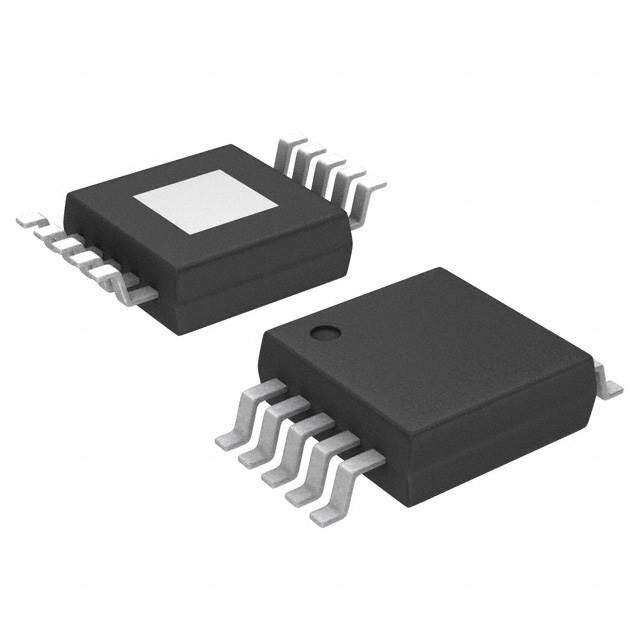
| 产品图片 |
|
| rohs | 符合RoHS无铅 / 符合限制有害物质指令(RoHS)规范要求 |
| 产品系列 | 电源管理 IC,稳压器—开关式稳压器,Texas Instruments TPS62042DGQ- |
| 数据手册 | |
| 产品型号 | TPS62042DGQ |
| PWM类型 | 电压模式 |
| 产品目录页面 | |
| 产品种类 | 稳压器—开关式稳压器 |
| 供应商器件封装 | 10-MSOP-PowerPad |
| 其它名称 | 296-27022-5 |
| 包装 | 管件 |
| 单位重量 | 23.500 mg |
| 同步整流器 | 是 |
| 商标 | Texas Instruments |
| 安装类型 | 表面贴装 |
| 安装风格 | SMD/SMT |
| 封装 | Tube |
| 封装/外壳 | 10-TFSOP,10-MSOP(0.118",3.00mm 宽)裸焊盘 |
| 封装/箱体 | HVSSOP-10 |
| 工作温度 | -40°C ~ 85°C |
| 工作温度范围 | - 40 C to + 85 C |
| 工厂包装数量 | 80 |
| 开关频率 | 1.25 MHz |
| 拓扑结构 | Buck |
| 最大工作温度 | + 85 C |
| 最大输入电压 | 6 V |
| 最小工作温度 | - 40 C |
| 最小输入电压 | 2.5 V |
| 标准包装 | 80 |
| 电压-输入 | 2.5 V ~ 6 V |
| 电压-输出 | 1.5V |
| 电流-输出 | 1.2A |
| 类型 | 降压(降压) |
| 系列 | TPS62042 |
| 输入电压 | 2.5 V to 6 V |
| 输出数 | 1 |
| 输出电压 | 1.5 V |
| 输出电流 | 1.2 A |
| 输出端数量 | 1 Output |
| 输出类型 | 固定 |
| 频率-开关 | 1.25MHz |


- 商务部:美国ITC正式对集成电路等产品启动337调查
- 曝三星4nm工艺存在良率问题 高通将骁龙8 Gen1或转产台积电
- 太阳诱电将投资9.5亿元在常州建新厂生产MLCC 预计2023年完工
- 英特尔发布欧洲新工厂建设计划 深化IDM 2.0 战略
- 台积电先进制程称霸业界 有大客户加持明年业绩稳了
- 达到5530亿美元!SIA预计今年全球半导体销售额将创下新高
- 英特尔拟将自动驾驶子公司Mobileye上市 估值或超500亿美元
- 三星加码芯片和SET,合并消费电子和移动部门,撤换高东真等 CEO
- 三星电子宣布重大人事变动 还合并消费电子和移动部门
- 海关总署:前11个月进口集成电路产品价值2.52万亿元 增长14.8%


PDF Datasheet 数据手册内容提取
TPS62040 TPS62042, TPS62043 TPS62044, TPS62046 www.ti.com SLVS463B − JUNE 2003 − REVISED OCTOBER 2005 1.2 A/1.25 MHz, HIGH-EFFICIENCY STEP-DOWN CONVERTER (cid:1) FEATURES USB Powered Modems (cid:1) (cid:1) CPUs and DSPs Up to 95% Conversion Efficiency (cid:1) (cid:1) Typical Quiescent Current: 18 µA PC Cards and Notebooks (cid:1) (cid:1) xDSL Applications Load Current: 1.2 A (cid:1) (cid:1) Standard 5-V to 3.3-V Conversion Operating Input Voltage Range: 2.5 V to 6.0 V (cid:1) Switching Frequency: 1.25 MHz DESCRIPTION (cid:1) Adjustable and Fixed Output Voltage (cid:1) Power Save Mode Operation at Light load The TPS6204x family of devices are high efficiency Currents synchronous step-down dc-dc converters optimized for (cid:1) battery powered portable applications. The devices are 100% Duty Cycle for Lowest Dropout ideal for portable applications powered by a single Li-Ion (cid:1) Internal Softstart battery cell or by 3-cell NiMH/NiCd batteries. With an (cid:1) Dynamic Output Voltage Positioning output voltage range from 6.0 V down to 0.7 V, the devices (cid:1) support low voltage DSPs and processors in PDAs, Thermal Shutdown (cid:1) pocket PCs, as well as notebooks and subnotebook Short-Circuit Protection computers. The TPS6204x operates at a fixed switching (cid:1) 10 Pin MSOP PowerPad™ Package frequency of 1.25 MHz and enters the power save mode (cid:1) 10 Pin QFN 3 X 3 mm Package operation at light load currents to maintain high efficiency over the entire load current range. For low noise applications, the devices can be forced into fixed APPLICATIONS frequency PWM mode by pulling the MODE pin high. The (cid:1) PDA, Pocket PC and Smart Phones TPS6204x supports up to 1.2-A load current. EFFICIENCY vs LOAD CURRENT 100 Typical Application Circuit 1.2-A Output Current VO = 1.8 V 95 VI = 2.7 V 90 VI TPS6204x L1 VO 85 VI = 3.6 V 2.5 V to 6 V 2 8 6.2 µH 0.7 V to VI /1.2 A % 80 VI = 5 V 22 CµF1 3146 VVMEIINONNDE PGSSNFWWBD 17950 C222 µF Efficiency − 677505 MODE = Low GND PGND 60 55 50 VI = 3.6 V 45 MODE = High 40 0 0.01 0.1 1 10 100 1 k 10 k IL − Load Current − mA Please be aware that an important notice concerning availability, standard warranty, and use in critical applications of TexasInstruments semiconductor products and disclaimers thereto appears at the end of this data sheet. PowerPAD is a trademark of Texas Instruments. PRODUCTION DATA information is current as of publication date. Products Copyright © 2003 − 2005, Texas Instruments Incorporated conform to specifications per the terms of Texas Instruments standard warranty. Production processing does not necessarily include testing of all parameters.
TPS62040 TPS62042, TPS62043 TPS62044, TPS62046 www.ti.com SLVS463B − JUNE 2003 − REVISED OCTOBER 2005 These devices have limited built-in ESD protection. The leads should be shorted together or the device placed in conductive foam during storage or handling to prevent electrostatic damage to the MOS gates. ORDERING INFORMATION PACKAGE PACKAGE MARKING TTA VVOOLLTTAAGGEE OOPPTTIIOONNSS MSOP(1) QFN(2) MSOP QFN Adjustable TPS62040DGQ TPS62040DRC BBI BBO 1.5 V TPS62042DGQ TPS62042DRC BBL BBS −4400°CC ttoo 8855°CC 1.6 V TPS62043DGQ TPS62043DRC BBM BBT 1.8 V TPS62044DGQ TPS62044DRC BBN BBU 3.3 V TPS62046DGQ TPS62046DRC BBQ BBW (1) The DGQ package is available in tape and reel. Add R suffix (DGQR) to order quantities of 2500 parts per reel. (2) The DRC package is available in tape and reel. Add R suffix (DRCR) to order quantities of 3000 parts per reel. ABSOLUTE MAXIMUM RATINGS over operating free-air temperature range unless otherwise noted(1) UNITS Supply voltage VIN (2) −0.3 V to 7 V Voltages on EN, MODE, FB, SW(2) −0.3 V to VCC +0.3 V Continuous power dissipation See Dissipation Rating Table Operating junction temperature range −40°C to 150°C Storage temperature range −65°C to 150°C Lead temperature (soldering, 10 sec) 260°C (1) Stresses beyond those listed under “absolute maximum ratings” may cause permanent damage to the device. These are stress ratings only, and functional operation of the device at these or any other conditions beyond those indicated under recommended operating conditions is not implied. Exposure to absolute-maximum-rated conditions for extended periods may affect device reliability. (2) All voltage values are with respect to network ground terminal. PACKAGE DISSIPATION RATINGS PACKAGE R(cid:1)JA(1) POWTAE R≤ 2R5A°CTING POWTAE R= 7R0A°CTING POWTAE R= 8R5A°CTING MSOP 60°C/W 1.67 W 917 mW 667 mW QFN 48.7°C/W 2.05 W 1.13 W 821 mW (1) The thermal resistance, RΘJA is based on a soldered PowerPAD using thermal vias. RECOMMENDED OPERATING CONDITIONS MIN TYP MAX UNIT VI Supply voltage 2.5 6.0 V VO Output voltage range for adjustable output voltage version 0.7 VI V IO Output current 1.2 A L Inductor(1) 6.2 µH CI Input capacitor(1) 22 µF CO Output capacitor(1) 22 µF TA Operating ambient temperature −40 85 °C TJ Operating junction temperature −40 125 °C (1) Refer to application section for further information 2
TPS62040 TPS62042, TPS62043 TPS62044, TPS62046 www.ti.com SLVS463B − JUNE 2003 − REVISED OCTOBER 2005 ELECTRICAL CHARACTERISTICS VI = 3.6 V, VO = 1.8 V, IO = 600 mA, EN = VIN, TA = −40°C to 85°C, typical values are at TA = 25°C (unless otherwise noted)(1) SUPPLY CURRENT PARAMETER TEST CONDITIONS MIN TYP MAX UNIT VI Input voltage range 2.5 6.0 V I(Q) Operating quiescent current IO = 0 mA, device is not switching 18 35 µA ISD Shutdown supply current EN = GND 0.1 1 µA VUVLO Under−voltage lockout threshold 1.5 2.3 V ENABLE AND MODE VEN EN high level input voltage 1.4 V VEN EN low level input voltage 0.4 V IEN EN input bias current EN = GND or VIN 0.01 1.0 µA V(MODE) MODE high level input voltage 1.4 V V(MODE) MODE low level input voltage 0.4 V I(MODE) MODE input bias current MODE = GND or VIN 0.01 1.0 µA POWER SWITCH P-channel MOSFET on−resistance VI = VGS = 3.6 V 115 210 mΩ rrDS(ON) P-channel MOSFET on−resistance VI = VGS = 2.5 V 145 270 mΩ Ilkg(P) P-channel leakage current VDS = 6.0 V 1 µA N-channel MOSFET on−resistance VI = VGS = 3.6 V 85 200 mΩ rrDS(ON) N-channel MOSFET on−resistance VI = VGS = 2.5 V 115 280 mΩ IIkg(N) N-channel leakage current VDS = 6.0 V 1 µA IL P-channel current limit 2.5 V < VI< 6.0 V 1.5 1.85 2.2 A Thermal shutdown 150 °C OSCILLATOR VFB = 0.5 V 1 1.25 1.5 MHz ffS OOsscciillllaattoorr ffrreeqquueennccyy VFB = 0 V 625 kHz OUTPUT VO Adjustable output voltage range TPS62040 0.7 VIN V Vref Reference voltage 0.5 V VFB Feedback voltage TAPdjSu6s2ta0b4le0 VVII == 22..55 VV ttoo 66..00 VV;; 0IO m= A0 m≤IAO ≤1.2 A −03%% 33%% TPS62042 VI = 2.5 V to 6.0 V; IO = 0 mA 0% 3% 1.5V VI = 2.5 V to 6.0 V; 0 mA ≤IO ≤1.2 A −3% 3% TPS62043 VI = 2.5 V to 6.0 V; IO = 0 mA 0% 3% 1.6V VI = 2.5 V to 6.0 V; 0 mA ≤IO ≤1.2 A −3% 3% VVO FFiixxeedd oouuttppuutt vvoollttaaggee TPS62044 VI = 2.5 V to 6.0 V; IO = 0 mA 0% 3% 1.8V VI = 2.5 V to 6.0 V; 0 mA ≤IO ≤1.2 A −3% 3% TPS62046 VI = 3.6 V to 6.0 V; IO = 0 mA 0% 3% 3.3V VI = 3.6 V to 6.0 V; 0 mA ≤IO ≤1.2 A −3% 3% Line regulation(1) VI = VO + 0.5 V (min. 2.5 V) to 6.0 V, 0 %/V IO = 10 mA Load regulation(1) IO = 10 mA to 1200 mA 0 %/mA Leakage current into SW pin VI>VO, 0 V ≤Vsw ≤VI 0.1 1 µA IIIkg(SW) Reverse leakage current into pin SW VI = open; EN = GND; VSW = 6.0 V 0.1 1 µA f Short circuit switching frequency VFB = 0 V 625 kHz (1) The line and load regulations are digitally controlled to assure an output voltage accuracy of ±3%. 3
TPS62040 TPS62042, TPS62043 TPS62044, TPS62046 www.ti.com SLVS463B − JUNE 2003 − REVISED OCTOBER 2005 PIN ASSIGNMENTS DGQ PACKAGE DRC PACKAGE (TOP VIEW) (TOP VIEW) EN 1 10 PGND EN 1 10 PGND VIN 2 9 PGND VIN 2 9 PGND VIN 3 8 SW VIN 3 8 SW GND 4 7 SW GND 4 7 SW FB 5 6 MODE FB 5 6 MODE NOTE: The PowerPAD must be connected to GND. Terminal Functions TERMINAL II//OO DDEESSCCRRIIPPTTIIOONN NAME NO. EN 1 I Enable. Pulling EN to ground forces the device into shutdown mode. Pulling EN to VI enables the device. EN should not be left floating and must be terminated. VIN 2,3 I Supply voltage input GND 4 Analog ground FB 5 I Feedback pin. Connect FB directly to the output if the fixed output voltage version is used. For the adjustable version an external resistor divider is connected to this pin. The internal voltage divider is disabled for the adjustable version. MODE 6 I Pulling the MODE pin high allows the device to be forced into fixed frequency operation. Pulling the MODE pin to low enables the power save mode where the device operates in fixed frequency PWM mode at high load currents and in PFM mode (pulse frequency modulation) at light load currents. SW 7,8 I/O This is the switch pin of the converter and is connected to the drain of the internal power MOSFETs PGND 9,10 Power ground 4
TPS62040 TPS62042, TPS62043 TPS62044, TPS62046 www.ti.com SLVS463B − JUNE 2003 − REVISED OCTOBER 2005 FUNCTIONAL BLOCK DIAGRAM VIN Current limit Comparator VIN Undervoltage + Lockout Bias supply − Ref EN Soft T + E Start SkipComparator nel SF − Ref an MO V Vcomp 1.25 MHz MODE P−Ch ower I Oscillator P Comparator S Driver SW Saw Tooth +− R Control Logic ShoLootg−itchru SW Generator Comp High Comp Low Comp Low 2 T E Comp High − LoadComparator annelMOSF Gm Compensation R1 + −Chwer + R2 No P Comp Low − + Comp Low 2 − Vref = 0.5 V MODE GND FB PGND PGND For the Adjustable Version the FB Pin Is Directly Connected to the Gm Amplifier 5
TPS62040 TPS62042, TPS62043 TPS62044, TPS62046 www.ti.com SLVS463B − JUNE 2003 − REVISED OCTOBER 2005 TYPICAL CHARACTERISTICS TABLE OF GRAPHS FIGURE η Efficiency vs Load current 1, 2, 3 η Efficiency vs Input voltage 4 IQ Quiescent current vs Input voltage 5, 6 fs Switching frequency vs Input voltage 7 rDS(on) P-Channel rDS(on) vs Input voltage 8 rDS(on) N-Channel rectifier rDS(on) vs Input voltage 9 Load transient response 10 PWM operation 11 Power save mode 12 Start-up 13 EFFICIENCY EFFICIENCY vs vs LOAD CURRENT LOAD CURRENT 100 100 VO = 3.3 V VO = 1.8 V 95 95 90 VI = 3.6 V 90 VI = 2.7 V MODE = Low 85 85 VI = 3.6 V 80 VMIO =D 5E V = Low 80 VI = 5 V % % − 75 − 75 ncy 70 VI = 3.6 V ncy 70 Efficie 65 MODE = High Efficie 65 MODE = Low VI = 3.6 V 60 VI = 5 V 60 MODE = High MODE = High 55 55 50 50 45 45 40 40 0 0.01 0.1 1 10 100 1 k 10 k 0 0.01 0.1 1 10 100 1 k 10 k IL − Load Current − mA IL − Load Current − mA Figure 1 Figure 2 6
TPS62040 TPS62042, TPS62043 TPS62044, TPS62046 www.ti.com SLVS463B − JUNE 2003 − REVISED OCTOBER 2005 EFFICIENCY EFFICIENCY vs vs LOAD CURRENT INPUT VOLTAGE 100 100 VO = 1.5 V VO = 1.8 V 95 MODE = Low 90 VI = 2.7 V 95 85 VI = 3.6 V IL = 500 mA 80 90 % % − 75 VI = 5 V − y y c c en 70 en 85 IL = 1000 mA Effici 65 Effici IL = 1 mA 60 80 55 50 75 45 70 40 0 0.01 0.1 1 10 100 1 k 10 k 2.5 3 3.5 4 4.5 5 5.5 6 IL − Load Current − mA VI − Input Voltage − V Figure 3 Figure 4 QUIESCENT CURRENT QUIESCENT CURRENT vs vs INPUT VOLTAGE INPUT VOLTAGE 23 7.5 MODE = Low MODE = High 21 TA = 85°C 7 19 6.5 µA TA = 25°C mA TA = 25°C nt − 17 nt − 6 urre 15 TA = −40°C urre 5.5 C C nt nt e 13 e 5 c c e e s s Qui 11 Qui 4.5 9 4 7 3.5 5 3 2.4 2.8 3.2 3.6 4 4.4 4.8 5.2 5.6 6 2.5 3 3.5 4 4.5 5 5.5 6 VI − Input Voltage − V VI − Input Voltage − V Figure 5 Figure 6 7
TPS62040 TPS62042, TPS62043 TPS62044, TPS62046 www.ti.com SLVS463B − JUNE 2003 − REVISED OCTOBER 2005 SWITCHING FREQUENCY P-CHANNEL r DS(on) vs vs INPUT VOLTAGE INPUT VOLTAGE 1.23 0.180 1.23 TA = 85°C 0.170 − MHz 11..2222 TA = 25°C Ωn) − 00..115600 TA = 85°C y o enc 1.21 DS( 0.140 TA = 25°C Frequ 1.21 TA = −40°C nnel r 0.130 witching 11..2200 P−Cha 00..111200 S 1.19 f − 0.100 TA = −40°C 1.19 1.18 0.090 1.18 0.080 2.5 2.9 3.3 3.7 4.1 4.5 4.9 5.3 5.7 6 2.5 2.9 3.3 3.7 4.1 4.5 4.9 5.3 5.7 6 VI − Input Voltage − V VI − Input Voltage − V Figure 7 Figure 8 N-CHANNEL RECTIFIER r DS(on) vs INPUT VOLTAGE 0.150 0.140 Ω − 0.130 n) TA = 85°C o 0.120 S( rD 0.110 TA = 25°C r e ctifi 0.100 e R el 0.090 n an 0.080 h C N- 0.070 TA = −40°C 0.060 0.050 2.5 2.9 3.3 3.7 4.1 4.5 4.9 5.3 5.7 6 VI − Input Voltage − V Figure 9 8
TPS62040 TPS62042, TPS62043 TPS62044, TPS62046 www.ti.com SLVS463B − JUNE 2003 − REVISED OCTOBER 2005 LOAD TRANSIENT RESPONSE PWM OPERATION VI = 3.6 V VO = 1.8 V PWM/PFM Operation Wdiv div VS5 V/ V/ VO0 m div 10 V/ Om V 0 2 A 15 div 1. A/ IOA to IL0 m m 50 0 5 1 50 µs/div 500 ns/div Figure 10 Figure 11 POWER SAVE MODE START-UP v ev Wdi bldi VS5 V/ Ena2 V/ v di OmV/ div V 20 VO1 V/ v di LmA/ div I 500 IIN0 mA/ VVIO = = 3 1.6.8 V V 20 IO = 1.1 A 2.5 µs/div 200 µs/div Figure 12 Figure 13 9
TPS62040 TPS62042, TPS62043 TPS62044, TPS62046 www.ti.com SLVS463B − JUNE 2003 − REVISED OCTOBER 2005 DETAILED DESCRIPTION OPERATION The TPS6204x is a synchronous step-down converter operating with typically 1.25 MHz fixed frequency. At moderate to heavy load currents, the device operates in pulse width modulation (PWM), and at light load currents, the device enters power save mode operation using pulse frequency modulation (PFM). When operating in PWM mode, the typical switching frequency is 1.25MHz with a minimum switching frequency of 1 MHz. This makes the device suitable for xDSL applications minimizing RF (radio frequency) interference. During PWM operation the converter uses a unique fast response voltage mode controller scheme with input voltage feed−forward to achieve good line and load regulation, allowing the use of small ceramic input and output capacitors. At the beginning of each clock cycle initiated by the clock signal (S) the P-channel MOSFET switch turns on and the inductor current ramps up until the comparator trips and the control logic turns off the switch. The current limit comparator also turns off the switch in case the current limit of the P-channel switch is exceeded. After the dead time preventing current shoot through, the N-channel MOSFET rectifier is turned on and the inductor current ramps down. The next cycle is initiated by the clock signal, again turning off the N-channel rectifier and turning on the P-channel switch. The Gm amplifier as well as the input voltage determines the rise time of the saw tooth generator, and therefore, any change in input voltage or output voltage directly controls the duty cycle of the converter, giving a very good line and load transient regulation. POWER SAVE MODE OPERATION As the load current decreases, the converter enters power save mode operation. During power save mode the converter operates with reduced switching frequency in PFM mode and with a minimum quiescent current maintaining high efficiency. The converter monitors the average inductor current and the device enters power save mode when the average inductor current is below the threshold. The transition point between PWM and power save mode is given by the transition current with the following equation: V I (cid:1) I transition 18.66(cid:1) (1) During power save mode the output voltage is monitored with the comparator by the threshold’s comp low and comp high. As the output voltage falls below the comp low threshold set to typically 0.8% above the nominal output voltage, the P-channel switch turns on. The P-channel switch remains on until the transition current (1) is reached. Then the N-channel switch turns on completing the first cycle. The converter continues to switch with its normal duty cycle determined by the input and output voltage but with half the nominal switching frequency of 625-kHz typ. Thus the output voltage rises and as soon as the output voltage reaches the comp high threshold of 1.6%, the converter stops switching. Depending on the load current, the converter switches for a longer or shorter period of time in order to deliver the energy to the output. If the load current increases and the output voltage can not be maintained with the transition current , equation (1), the converter enters PWM again. See Figure 11 and Figure 12 under the typical graphs section and Figure 14 for power save mode operation. Among other techniques this advanced power save mode method allows high efficiency over the entire load current range and a small output ripple of typically 1% of the nominal output voltage. Setting the power save mode thresholds to typically 0.8% and 1.6% above the nominal output voltage at light load current results in a dynamic voltage positioning achieving lower absolute voltage drops during heavy load transient changes. This allows the converter to operate with small output capacitors like 22 µF and still having a low absolute voltage drop during heavy load transient. Refer to Figure 14 as well for detailed operation of the power save mode. 10
TPS62040 TPS62042, TPS62043 TPS62044, TPS62046 www.ti.com SLVS463B − JUNE 2003 − REVISED OCTOBER 2005 PFM Mode at Light Load 1.6% Comp High 0.8% Comp Low VO Comp Low 2 PWM Mode at Medium to Full Load Figure 14. Power Save Mode Thresholds and Dynamic Voltage Positioning The converter enters the fixed frequency PWM mode as soon as the output voltage falls below the comp low 2 threshold. DYNAMIC VOLTAGE POSITIONING As described in the power save mode operation sections before and as detailed in Figure 14 the output voltage is typically 0.8% (i.e., 1% on average) above the nominal output voltage at light load currents, as the device is in power save mode. This gives additional headroom for the voltage drop during a load transient from light load to full load. In the other direction during a load transient from full load to light load the voltage overshoot is also minimized by turning on the N-Channel rectifier switch to pull the output voltage actively down. MODE (AUTOMATIC PWM/PFM OPERATION AND FORCED PWM OPERATION) Connecting the MODE pin to GND enables the automatic PWM and power save mode operation. The converter operates in fixed frequency PWM mode at moderate to heavy loads and in the PFM mode during light loads, maintaining high efficiency over a wide load current range. Pulling the MODE pin high forces the converter to operate constantly in the PWM mode even at light load currents. The advantage is the converter operates with a fixed switching frequency that allows simple filtering of the switching frequency for noise sensitive applications. In this mode, the efficiency is lower compared to the power save mode during light loads (see Figure 1 to Figure 3). For additional flexibility it is possible to switch from power save mode to forced PWM mode during operation. This allows efficient power management by adjusting the operation of the TPS6204x to the specific system requirements. 100% DUTY CYCLE LOW DROPOUT OPERATION The TPS6204x offers a low input to output voltage difference while still maintaining regulation with the use of the 100% duty cycle mode. In this mode, the P−Channel switch is constantly turned on. This is particularly useful in battery powered applications to achieve longest operation time by taking full advantage of the whole battery voltage range. i.e. The minimum input voltage to maintain regulation depends on the load current and output voltage and can be calculated as: (cid:4) (cid:5) V min(cid:1)V max(cid:2)I max(cid:3) r max(cid:2)R I O O DS(on) L (2) with: I = maximum output current plus inductor ripple current O(max) r max= maximum P-channel switch t . DS(on) DS(on) R = DC resistance of the inductor L V max = nominal output voltage plus maximum output voltage tolerance O 11
TPS62040 TPS62042, TPS62043 TPS62044, TPS62046 www.ti.com SLVS463B − JUNE 2003 − REVISED OCTOBER 2005 SOFTSTART The TPS6204x series has an internal softstart circuit that limits the inrush current during start up. This prevents possible voltage drops of the input voltage in case a battery or a high impedance power source is connected to the input of the TPS6204x. The softstart is implemented with a digital circuit increasing the switch current in steps of typically I /8, I /4, I /2 LIM LIM LIM and then the typical switch current limit 1.85 A as specified in the electrical parameter table. The start-up time mainly depends on the output capacitor and load current, see Figure 13. SHORT-CIRCUIT PROTECTION As soon as the output voltage falls below 50% of the nominal output voltage, the converter switching frequency as well as the current limit is reduced to 50% of the nominal value. Since the short-circuit protection is enabled during start-up, the device does not deliver more than half of its nominal current limit until the output voltage exceeds 50% of the nominal output voltage. This needs to be considered in case a load acting as a current sink is connected to the output of the converter. THERMAL SHUTDOWN As soon as the junction temperature of typically 150(cid:2)C is exceeded the device goes into thermal shutdown. In this mode, the P-Channel switch and N-Channel rectifier are turned off. The device continues its operation when the junction temperature falls below typically 150°C again. ENABLE Pulling the EN low forces the part into shutdown mode, with a shutdown current of typically 0.1 µA. In this mode, the P-Channel switch and N-Channel rectifier are turned off and the whole device is in shut down. If an output voltage is present during shut down, which could be an external voltage source or super cap, the reverse leakage current is specified under electrical parameter table. For proper operation the enable (EN) pin must be terminated and should not be left floating. Pulling EN high starts up the TPS6204x with the softstart as described under the section Softstart. UNDERVOLTAGE LOCKOUT The undervoltage lockout circuit prevents device misoperation at low input voltages. It prevents the converter from turning on the switch or rectifier MOSFET with undefined conditions. 12
TPS62040 TPS62042, TPS62043 TPS62044, TPS62046 www.ti.com SLVS463B − JUNE 2003 − REVISED OCTOBER 2005 APPLICATION INFORMATION ADJUSTABLE OUTPUT VOLTAGE VERSION When the adjustable output voltage version TPS62040 is used, the output voltage is set by the external resistor divider. See Figure 15. The output voltage is calculated as: (cid:4) (cid:5) V (cid:1)0.5V(cid:3) 1(cid:2)R1 O R2 (3) with R1 + R2 ≤1 MΩ and internal reference voltage V typical = 0.5 V ref R1 + R2 should not be greater than 1 MΩ because of stability reasons. To keep the operating quiescent current to a minimum, the feedback resistor divider should have high impedance with R1+R2≤1 MΩ. Due to this and the low reference voltage of Vref = 0.5 V, the noise on the feedback pin (FB) needs to be minimized. Using a capacitive divider C1 and C2 across the feedback resistors minimizes the noise at the feedback, without degrading the line or load transient performance. C1 and C2 should be selected as: C1(cid:1) 1 2(cid:3)(cid:2)(cid:3)10kHz(cid:3)R1 (4) with: R1 = upper resistor of voltage divider C1 = upper capacitor of voltage divider For C1 a value should be chosen that comes closest to the calculated result. C2(cid:1)R1(cid:3)C1 R2 (5) with: R2 = lower resistor of voltage divider C2 = lower capacitor of voltage divider For C2, the selected capacitor value should always be selected larger than the calculated result. For example, in Figure 15 for C2 100 pF are selected for a calculated result of C2 = 88.42 pF. If quiescent current is not a key design parameter C1 and C2 can be omitted, and a low impedance feedback divider has to be used with R1 + R2 < 100 kΩ. This reduces the noise available on the feedback pin (FB) as well but increases the overall quiescent current during operation. The higher the programmed output voltage the lower the feedback impedance has to be for best operation when not using C1 and C2. VI TPS62040 L1 VO 2.5 V to 6 V 2 8 10 µH 1.8 V / 1.2 A VIN SW 3 7 10 CµF3 1 VEINN SFWB 5 R1 C1 C104 µF 6 MODE PGND 10 470 kΩ 33 pF 4 9 GND PGND R2 180 kΩ C2 100 pF Figure 15. Adjustable Output Voltage Version 13
TPS62040 TPS62042, TPS62043 TPS62044, TPS62046 www.ti.com SLVS463B − JUNE 2003 − REVISED OCTOBER 2005 Inductor Selection The TPS6204x typically uses a 6.2-µH output inductor. Larger or smaller inductor values can be used to optimize the performance of the device for specific operation conditions. The selected inductor has to be rated for its dc resistance and saturation current. The dc resistance of the inductance directly influences the efficiency of the converter. Therefore an inductor with the lowest dc resistance should be selected for highest efficiency. Formula (7) calculates the maximum inductor current under static load conditions. The saturation current of the inductor should be rated higher than the maximum inductor current as calculated with formula (7). This is needed because during heavy load transient the inductor current rises above the value calculated under (7). V O 1– V (cid:3)I (cid:1)V (cid:3) I L O L(cid:3)ƒ (6) (cid:3)I I max(cid:1)I max(cid:2) L L O 2 (7) with ƒ = Switching frequency (1.25 MHz typical) L = Inductor value ∆I = Peak-to-peak inductor ripple current L I max = Maximum inductor current L The highest inductor current occurs at maximum V. I Open core inductors have a soft saturation characteristic and they can usually handle higher inductor currents versus a comparable shielded inductor. A more conservative approach is to select the inductor current rating just for the maximum switch current of 2.2 A for the TPS6204x. Keep in mind that the core material from inductor to inductor differs and has an impact on the efficiency, especially at high switching frequencies. Refer to Table 1 and the typical applications and inductors selection. Table 1. Inductor Selection INDUCTOR VALUE DIMENSIONS COMPONENT SUPPLIER 4.7 µH 5,0 mm × 5,0 mm × 3,0 mm Sumida CDRH4D28C-4.7 4.7 µH 5,2 mm × 5,2 mm × 2,5 mm Coiltronics SD25-4R7 5.3 µH 5,7 mm × 5,7 mm × 3,0 mm Sumida CDRH5D28-5R3 6.2 µH 5,7 mm × 5,7 mm × 3,0 mm Sumida CDRH5D28-6R2 6.0 µH 7,0 mm × 7,0 mm × 3,0 mm Sumida CDRH6D28-6R0 14
TPS62040 TPS62042, TPS62043 TPS62044, TPS62046 www.ti.com SLVS463B − JUNE 2003 − REVISED OCTOBER 2005 Output Capacitor Selection The advanced fast response voltage mode control scheme of the TPS6204x allows the use of small ceramic capacitors with a typical value of 22 µF without having large output voltage under and overshoots during heavy load transients. Ceramic capacitors having low ESR values have the lowest output voltage ripple and are recommended. If required, tantalum capacitors may also be used. Refer to Table 2 for component selection. If ceramic output capacitor are used, the capacitor RMS ripple current rating always meets the application requirements. Just for completeness the RMS ripple current is calculated as: V O 1– V I (cid:1)V (cid:3) I (cid:3) 1 RMSCout O L(cid:3)ƒ 2(cid:3)(cid:6)3 (8) At nominal load current the device operates in PWM mode and the overall output voltage ripple is the sum of the voltage spike caused by the output capacitor ESR plus the voltage ripple caused by charging and discharging the output capacitor: V O (cid:4) (cid:5) 1– V (cid:3)V (cid:1)V (cid:3) I (cid:3) 1 (cid:2)ESR O O L(cid:3)ƒ 8(cid:3)C (cid:3)ƒ O (9) Where the highest output voltage ripple occurs at the highest input voltage, V. I At light load currents, the device operates in power save mode and the output voltage ripple is independent of the output capacitor value. The output voltage ripple is set by the internal comparator thresholds. The typical output voltage ripple is 1% of the nominal output voltage. Input Capacitor Selection Because of the nature of the buck converter having a pulsating input current, a low ESR input capacitor is required for best input voltage filtering and minimizing the interference with other circuits caused by high input voltage spikes. The input capacitor should have a minimum value of 22 µF. The input capacitor can be increased without any limit for better input voltage filtering. Table 2. Input and Output Capacitor Selection CAPACITOR CASE SIZE COMPONENT SUPPLIER COMMENTS VALUE 22 µF 1206 Taiyo Yuden JMK316BJ226ML Ceramic 22 µF 1210 Taiyo Yuden JMK325BJ226MM Ceramic 15
TPS62040 TPS62042, TPS62043 TPS62044, TPS62046 www.ti.com SLVS463B − JUNE 2003 − REVISED OCTOBER 2005 Layout Considerations For all switching power supplies, the layout is an important step in the design especially at high peak currents and switching frequencies. If the layout is not carefully done, the regulator might show stability problems as well as EMI problems. Therefore, use wide and short traces for the main current paths as indicated in bold in Figure 16. These traces should be routed first. The input capacitor should be placed as close as possible to the IC pins as well as the inductor and output capacitor. The feedback resistor network should be routed away from the inductor and switch node to minimize noise and magnetic interference. To further minimize noise from coupling into the feedback network and feedback pin, the ground plane or ground traces should be used for shielding. A common ground plane or a star ground as shown below should be used. This becomes very important especially at high switching frequencies of 1.25 MHz. The Switch Node Must Be Kept as Small as Possible TPS6204x L1 VI 2 8 10 µH VO VIN SW 3 7 22 CµF3 1 VEINN SFWB 5 C222 µF 6 10 MODE PGND 4 9 GND PGND Figure 16. Layout Diagram THERMAL INFORMATION One of the most influential components on the thermal performance of a package is board design. In order to take full advantage of the heat dissipating abilities of the PowerPAD(cid:3) packages, a board should be used that acts similar to a heat sink and allows for the use of the exposed (and solderable), deep downset pad. For further information please refer to Texas Instruments application note (SLMA002) PowerPAD Thermally Enhanced Package. The PowerPAD(cid:3) of the 10-pin MSOP package has an area of 1,52 mm × 1,79 mm (± 0,05 mm) and must be soldered to the PCB to lower the thermal resistance. Thermal vias to the next layer further reduce the thermal resistance. 16
TPS62040 TPS62042, TPS62043 TPS62044, TPS62046 www.ti.com SLVS463B − JUNE 2003 − REVISED OCTOBER 2005 TYPICAL APPLICATIONS VI TPS62046 L1 VO Li-lon 2 8 6.2 µH 3.3 V / 1.2 A VIN SW 3 7 C1 VIN SW C2 1 5 22 µF EN FB 22 µF 6 10 MODE PGND 4 9 GND PGND Components: C1: Taiyo Yuden JMK316BJ226ML C2: Taiyo Yuden JMK316BJ226ML L1: Sumida CDRH5D28−6R2 Figure 17. Li-Ion to 3.3 V/1.2 A Conversion VI TPS62040 L1 VO 2.5 V to 6 V 2 8 4.7 µH 1.8 V / 1.2 A VIN SW 22 CµF3 31 VEINN SFWB 57 R1 C1 C224 µF 6 MODE PGND10 470 kΩ 33 pF 4 9 GND PGND Components: C1: Taiyo Yuden JMK316BJ226ML R2 C2 C2: Taiyo Yuden JMK316BJ226ML 180 kΩ 100 pF L1: Sumida CDRH4D28C−4R7 Figure 18. Li-Ion to 1.8 V/1.2 A Conversion Using the Adjustable Output Voltage Version 17
PACKAGE OPTION ADDENDUM www.ti.com 6-Feb-2020 PACKAGING INFORMATION Orderable Device Status Package Type Package Pins Package Eco Plan Lead/Ball Finish MSL Peak Temp Op Temp (°C) Device Marking Samples (1) Drawing Qty (2) (6) (3) (4/5) TPS62040DGQ ACTIVE HVSSOP DGQ 10 80 Green (RoHS NIPDAUAG Level-1-260C-UNLIM -40 to 85 BBI & no Sb/Br) TPS62040DGQG4 ACTIVE HVSSOP DGQ 10 80 Green (RoHS NIPDAUAG Level-1-260C-UNLIM -40 to 85 BBI & no Sb/Br) TPS62040DGQR ACTIVE HVSSOP DGQ 10 2500 Green (RoHS NIPDAUAG Level-1-260C-UNLIM -40 to 85 BBI & no Sb/Br) TPS62040DGQRG4 ACTIVE HVSSOP DGQ 10 2500 Green (RoHS NIPDAUAG Level-1-260C-UNLIM -40 to 85 BBI & no Sb/Br) TPS62040DRCR ACTIVE VSON DRC 10 3000 Green (RoHS NIPDAU Level-2-260C-1 YEAR -40 to 85 BBO & no Sb/Br) TPS62040DRCRG4 ACTIVE VSON DRC 10 3000 Green (RoHS NIPDAU Level-2-260C-1 YEAR -40 to 85 BBO & no Sb/Br) TPS62042DGQ ACTIVE HVSSOP DGQ 10 80 Green (RoHS NIPDAUAG Level-1-260C-UNLIM -40 to 85 BBL & no Sb/Br) TPS62042DGQG4 ACTIVE HVSSOP DGQ 10 80 Green (RoHS NIPDAUAG Level-1-260C-UNLIM -40 to 85 BBL & no Sb/Br) TPS62042DGQR ACTIVE HVSSOP DGQ 10 2500 Green (RoHS NIPDAUAG Level-1-260C-UNLIM -40 to 85 BBL & no Sb/Br) TPS62042DGQRG4 ACTIVE HVSSOP DGQ 10 2500 Green (RoHS NIPDAUAG Level-1-260C-UNLIM -40 to 85 BBL & no Sb/Br) TPS62042DRCR ACTIVE VSON DRC 10 3000 Green (RoHS NIPDAU Level-2-260C-1 YEAR -40 to 85 BBS & no Sb/Br) TPS62042DRCRG4 ACTIVE VSON DRC 10 3000 Green (RoHS NIPDAU Level-2-260C-1 YEAR -40 to 85 BBS & no Sb/Br) TPS62043DGQ ACTIVE HVSSOP DGQ 10 80 Green (RoHS NIPDAUAG Level-1-260C-UNLIM -40 to 85 BBM & no Sb/Br) TPS62043DGQR ACTIVE HVSSOP DGQ 10 2500 Green (RoHS NIPDAUAG Level-1-260C-UNLIM -40 to 85 BBM & no Sb/Br) TPS62043DRCR ACTIVE VSON DRC 10 3000 Green (RoHS NIPDAU Level-2-260C-1 YEAR -40 to 85 BBT & no Sb/Br) TPS62044DGQ ACTIVE HVSSOP DGQ 10 80 Green (RoHS NIPDAUAG Level-1-260C-UNLIM -40 to 85 BBN & no Sb/Br) TPS62044DGQG4 ACTIVE HVSSOP DGQ 10 80 Green (RoHS NIPDAUAG Level-1-260C-UNLIM -40 to 85 BBN & no Sb/Br) Addendum-Page 1
PACKAGE OPTION ADDENDUM www.ti.com 6-Feb-2020 Orderable Device Status Package Type Package Pins Package Eco Plan Lead/Ball Finish MSL Peak Temp Op Temp (°C) Device Marking Samples (1) Drawing Qty (2) (6) (3) (4/5) TPS62044DGQR ACTIVE HVSSOP DGQ 10 2500 Green (RoHS NIPDAUAG Level-1-260C-UNLIM -40 to 85 BBN & no Sb/Br) TPS62044DGQRG4 ACTIVE HVSSOP DGQ 10 2500 Green (RoHS NIPDAUAG Level-1-260C-UNLIM -40 to 85 BBN & no Sb/Br) TPS62044DRCR ACTIVE VSON DRC 10 3000 Green (RoHS NIPDAU Level-2-260C-1 YEAR -40 to 85 BBU & no Sb/Br) TPS62046DGQ ACTIVE HVSSOP DGQ 10 80 Green (RoHS NIPDAUAG Level-1-260C-UNLIM -40 to 85 BBQ & no Sb/Br) TPS62046DGQR ACTIVE HVSSOP DGQ 10 2500 Green (RoHS NIPDAUAG Level-1-260C-UNLIM -40 to 85 BBQ & no Sb/Br) TPS62046DGQRG4 ACTIVE HVSSOP DGQ 10 2500 Green (RoHS NIPDAUAG Level-1-260C-UNLIM -40 to 85 BBQ & no Sb/Br) TPS62046DRCR ACTIVE VSON DRC 10 3000 Green (RoHS NIPDAU Level-2-260C-1 YEAR -40 to 85 BBW & no Sb/Br) (1) The marketing status values are defined as follows: ACTIVE: Product device recommended for new designs. LIFEBUY: TI has announced that the device will be discontinued, and a lifetime-buy period is in effect. NRND: Not recommended for new designs. Device is in production to support existing customers, but TI does not recommend using this part in a new design. PREVIEW: Device has been announced but is not in production. Samples may or may not be available. OBSOLETE: TI has discontinued the production of the device. (2) RoHS: TI defines "RoHS" to mean semiconductor products that are compliant with the current EU RoHS requirements for all 10 RoHS substances, including the requirement that RoHS substance do not exceed 0.1% by weight in homogeneous materials. Where designed to be soldered at high temperatures, "RoHS" products are suitable for use in specified lead-free processes. TI may reference these types of products as "Pb-Free". RoHS Exempt: TI defines "RoHS Exempt" to mean products that contain lead but are compliant with EU RoHS pursuant to a specific EU RoHS exemption. Green: TI defines "Green" to mean the content of Chlorine (Cl) and Bromine (Br) based flame retardants meet JS709B low halogen requirements of <=1000ppm threshold. Antimony trioxide based flame retardants must also meet the <=1000ppm threshold requirement. (3) MSL, Peak Temp. - The Moisture Sensitivity Level rating according to the JEDEC industry standard classifications, and peak solder temperature. (4) There may be additional marking, which relates to the logo, the lot trace code information, or the environmental category on the device. (5) Multiple Device Markings will be inside parentheses. Only one Device Marking contained in parentheses and separated by a "~" will appear on a device. If a line is indented then it is a continuation of the previous line and the two combined represent the entire Device Marking for that device. Addendum-Page 2
PACKAGE OPTION ADDENDUM www.ti.com 6-Feb-2020 (6) Lead/Ball Finish - Orderable Devices may have multiple material finish options. Finish options are separated by a vertical ruled line. Lead/Ball Finish values may wrap to two lines if the finish value exceeds the maximum column width. Important Information and Disclaimer:The information provided on this page represents TI's knowledge and belief as of the date that it is provided. TI bases its knowledge and belief on information provided by third parties, and makes no representation or warranty as to the accuracy of such information. Efforts are underway to better integrate information from third parties. TI has taken and continues to take reasonable steps to provide representative and accurate information but may not have conducted destructive testing or chemical analysis on incoming materials and chemicals. TI and TI suppliers consider certain information to be proprietary, and thus CAS numbers and other limited information may not be available for release. In no event shall TI's liability arising out of such information exceed the total purchase price of the TI part(s) at issue in this document sold by TI to Customer on an annual basis. Addendum-Page 3
PACKAGE MATERIALS INFORMATION www.ti.com 17-Jul-2020 TAPE AND REEL INFORMATION *Alldimensionsarenominal Device Package Package Pins SPQ Reel Reel A0 B0 K0 P1 W Pin1 Type Drawing Diameter Width (mm) (mm) (mm) (mm) (mm) Quadrant (mm) W1(mm) TPS62040DGQR HVSSOP DGQ 10 2500 330.0 12.4 5.3 3.4 1.4 8.0 12.0 Q1 TPS62040DRCR VSON DRC 10 3000 330.0 12.4 3.3 3.3 1.0 8.0 12.0 Q2 TPS62040DRCR VSON DRC 10 3000 330.0 12.4 3.3 3.3 1.1 8.0 12.0 Q2 TPS62040DRCR VSON DRC 10 3000 330.0 12.4 3.3 3.3 1.1 8.0 12.0 Q2 TPS62042DGQR HVSSOP DGQ 10 2500 330.0 12.4 5.3 3.4 1.4 8.0 12.0 Q1 TPS62042DRCR VSON DRC 10 3000 330.0 12.4 3.3 3.3 1.1 8.0 12.0 Q2 TPS62043DGQR HVSSOP DGQ 10 2500 330.0 12.4 5.3 3.4 1.4 8.0 12.0 Q1 TPS62043DRCR VSON DRC 10 3000 330.0 12.4 3.3 3.3 1.0 8.0 12.0 Q2 TPS62043DRCR VSON DRC 10 3000 330.0 12.4 3.3 3.3 1.1 8.0 12.0 Q2 TPS62044DGQR HVSSOP DGQ 10 2500 330.0 12.4 5.3 3.4 1.4 8.0 12.0 Q1 TPS62044DRCR VSON DRC 10 3000 330.0 12.4 3.3 3.3 1.1 8.0 12.0 Q2 TPS62046DGQR HVSSOP DGQ 10 2500 330.0 12.4 5.3 3.4 1.4 8.0 12.0 Q1 TPS62046DRCR VSON DRC 10 3000 330.0 12.4 3.3 3.3 1.0 8.0 12.0 Q2 TPS62046DRCR VSON DRC 10 3000 330.0 12.4 3.3 3.3 1.1 8.0 12.0 Q2 PackMaterials-Page1
PACKAGE MATERIALS INFORMATION www.ti.com 17-Jul-2020 *Alldimensionsarenominal Device PackageType PackageDrawing Pins SPQ Length(mm) Width(mm) Height(mm) TPS62040DGQR HVSSOP DGQ 10 2500 364.0 364.0 27.0 TPS62040DRCR VSON DRC 10 3000 370.0 355.0 55.0 TPS62040DRCR VSON DRC 10 3000 367.0 367.0 35.0 TPS62040DRCR VSON DRC 10 3000 367.0 367.0 35.0 TPS62042DGQR HVSSOP DGQ 10 2500 364.0 364.0 27.0 TPS62042DRCR VSON DRC 10 3000 367.0 367.0 35.0 TPS62043DGQR HVSSOP DGQ 10 2500 364.0 364.0 27.0 TPS62043DRCR VSON DRC 10 3000 370.0 355.0 55.0 TPS62043DRCR VSON DRC 10 3000 367.0 367.0 35.0 TPS62044DGQR HVSSOP DGQ 10 2500 364.0 364.0 27.0 TPS62044DRCR VSON DRC 10 3000 367.0 367.0 35.0 TPS62046DGQR HVSSOP DGQ 10 2500 364.0 364.0 27.0 TPS62046DRCR VSON DRC 10 3000 370.0 355.0 55.0 TPS62046DRCR VSON DRC 10 3000 367.0 367.0 35.0 PackMaterials-Page2
None
None
None
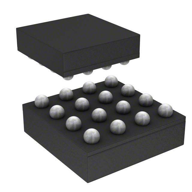
GENERIC PACKAGE VIEW DRC 10 VSON - 1 mm max height PLASTIC SMALL OUTLINE - NO LEAD Images above are just a representation of the package family, actual package may vary. Refer to the product data sheet for package details. 4204102-3/M
PACKAGE OUTLINE DRC0010J VSON - 1 mm max height SCALE 4.000 PLASTIC SMALL OUTLINE - NO LEAD 3.1 B A 2.9 PIN 1 INDEX AREA 3.1 2.9 1.0 C 0.8 SEATING PLANE 0.05 0.00 0.08 C 1.65 0.1 2X (0.5) (0.2) TYP EXPOSED 4X (0.25) THERMAL PAD 5 6 2X 11 SYMM 2 2.4 0.1 10 1 8X 0.5 0.30 10X 0.18 PIN 1 ID SYMM 0.1 C A B (OPTIONAL) 0.5 0.05 C 10X 0.3 4218878/B 07/2018 NOTES: 1. All linear dimensions are in millimeters. Any dimensions in parenthesis are for reference only. Dimensioning and tolerancing per ASME Y14.5M. 2. This drawing is subject to change without notice. 3. The package thermal pad must be soldered to the printed circuit board for optimal thermal and mechanical performance. www.ti.com
EXAMPLE BOARD LAYOUT DRC0010J VSON - 1 mm max height PLASTIC SMALL OUTLINE - NO LEAD (1.65) (0.5) 10X (0.6) 1 10 10X (0.24) 11 SYMM (2.4) (3.4) (0.95) 8X (0.5) 6 5 (R0.05) TYP ( 0.2) VIA TYP (0.25) (0.575) SYMM (2.8) LAND PATTERN EXAMPLE EXPOSED METAL SHOWN SCALE:20X 0.07 MIN 0.07 MAX EXPOSED METAL ALL AROUND ALL AROUND EXPOSED METAL SOLDER MASK METAL METAL UNDER SOLDER MASK OPENING SOLDER MASK OPENING NON SOLDER MASK SOLDER MASK DEFINED DEFINED (PREFERRED) SOLDER MASK DETAILS 4218878/B 07/2018 NOTES: (continued) 4. This package is designed to be soldered to a thermal pad on the board. For more information, see Texas Instruments literature number SLUA271 (www.ti.com/lit/slua271). 5. Vias are optional depending on application, refer to device data sheet. If any vias are implemented, refer to their locations shown on this view. It is recommended that vias under paste be filled, plugged or tented. www.ti.com
EXAMPLE STENCIL DESIGN DRC0010J VSON - 1 mm max height PLASTIC SMALL OUTLINE - NO LEAD 2X (1.5) (0.5) SYMM EXPOSED METAL 11 TYP 10X (0.6) 1 10 (1.53) 10X (0.24) 2X (1.06) SYMM (0.63) 8X (0.5) 6 5 (R0.05) TYP 4X (0.34) 4X (0.25) (2.8) SOLDER PASTE EXAMPLE BASED ON 0.125 mm THICK STENCIL EXPOSED PAD 11: 80% PRINTED SOLDER COVERAGE BY AREA SCALE:25X 4218878/B 07/2018 NOTES: (continued) 6. Laser cutting apertures with trapezoidal walls and rounded corners may offer better paste release. IPC-7525 may have alternate design recommendations. www.ti.com
IMPORTANTNOTICEANDDISCLAIMER TI PROVIDES TECHNICAL AND RELIABILITY DATA (INCLUDING DATASHEETS), DESIGN RESOURCES (INCLUDING REFERENCE DESIGNS), APPLICATION OR OTHER DESIGN ADVICE, WEB TOOLS, SAFETY INFORMATION, AND OTHER RESOURCES “AS IS” AND WITH ALL FAULTS, AND DISCLAIMS ALL WARRANTIES, EXPRESS AND IMPLIED, INCLUDING WITHOUT LIMITATION ANY IMPLIED WARRANTIES OF MERCHANTABILITY, FITNESS FOR A PARTICULAR PURPOSE OR NON-INFRINGEMENT OF THIRD PARTY INTELLECTUAL PROPERTY RIGHTS. These resources are intended for skilled developers designing with TI products. You are solely responsible for (1) selecting the appropriate TI products for your application, (2) designing, validating and testing your application, and (3) ensuring your application meets applicable standards, and any other safety, security, or other requirements. These resources are subject to change without notice. TI grants you permission to use these resources only for development of an application that uses the TI products described in the resource. Other reproduction and display of these resources is prohibited. No license is granted to any other TI intellectual property right or to any third party intellectual property right. TI disclaims responsibility for, and you will fully indemnify TI and its representatives against, any claims, damages, costs, losses, and liabilities arising out of your use of these resources. TI’s products are provided subject to TI’s Terms of Sale (www.ti.com/legal/termsofsale.html) or other applicable terms available either on ti.com or provided in conjunction with such TI products. TI’s provision of these resources does not expand or otherwise alter TI’s applicable warranties or warranty disclaimers for TI products. Mailing Address: Texas Instruments, Post Office Box 655303, Dallas, Texas 75265 Copyright © 2020, Texas Instruments Incorporated