ICGOO在线商城 > 集成电路(IC) > PMIC - 稳压器 - DC DC 开关稳压器 > TPS61220DCKT
 Datasheet下载
- 型号: TPS61220DCKT
- 制造商: Texas Instruments
- 库位|库存: xxxx|xxxx
- 要求:
| 数量阶梯 | 香港交货 | 国内含税 |
| +xxxx | $xxxx | ¥xxxx |
查看当月历史价格
查看今年历史价格
TPS61220DCKT产品简介:
ICGOO电子元器件商城为您提供TPS61220DCKT由Texas Instruments设计生产,在icgoo商城现货销售,并且可以通过原厂、代理商等渠道进行代购。 TPS61220DCKT价格参考。Texas InstrumentsTPS61220DCKT封装/规格:PMIC - 稳压器 - DC DC 开关稳压器, 可调式 升压 开关稳压器 IC 正 1.8V 1 输出 200mA(开关) 6-TSSOP,SC-88,SOT-363。您可以下载TPS61220DCKT参考资料、Datasheet数据手册功能说明书,资料中有TPS61220DCKT 详细功能的应用电路图电压和使用方法及教程。
TPS61220DCKT 是 Texas Instruments(德州仪器)推出的一款 PMIC - DC/DC 开关稳压器。该器件属于升压转换器系列,能够将较低的输入电压转换为更高的输出电压,适用于多种便携式和电池供电设备的应用场景。以下是 TPS61220DCKT 的主要应用场景:

 1. 便携式电子设备
   - 移动电源和充电宝:TPS61220DCKT 可以将单节锂电池(典型电压 3.6V 或 3.7V)的电压提升到 5V,用于为 USB 设备充电。
   - 蓝牙耳机和音箱:在小型音频设备中,这款芯片可以提供稳定的电压输出,确保音频质量不受电池电压下降的影响。
   - 智能手表和健身追踪器:这些设备通常依赖小容量电池,TPS61220DCKT 可以高效地将电池电压提升至所需水平,延长设备续航时间。

 2. 物联网 (IoT) 设备
   - 传感器模块:在低功耗 IoT 应用中,TPS61220DCKT 能够为传感器提供稳定的电源,支持无线通信模块(如 Zigbee、LoRa 或 BLE)正常工作。
   - 环境监测设备:例如温湿度传感器或气体检测仪,这些设备通常需要稳定的电源供应,而 TPS61220DCKT 可以从电池或能量收集系统中获取足够的电能。

 3. 消费类电子产品
   - 电子阅读器和手持游戏机:通过高效的升压转换,确保设备在电池电量较低时仍能保持正常运行。
   - 数码相机和摄像机:为相机中的图像处理单元或其他高功率组件提供稳定的电源支持。

 4. 工业应用
   - 无线遥控器和数据采集设备:在工业自动化领域,TPS61220DCKT 可以为远程控制单元或数据记录器提供可靠的电源。
   - 便携式测试仪器:例如万用表或示波器,这些设备通常需要稳定的电源来保证测量精度。

 5. 医疗设备
   - 便携式健康监测设备:如血糖仪、脉搏血氧仪等,TPS61220DCKT 可以确保设备在不同电池状态下的稳定性能。

 核心优势
- 高效转换:高达 90% 的转换效率,减少热量损耗,延长电池寿命。
- 小尺寸封装:适合空间受限的设计,便于集成到紧凑型设备中。
- 宽输入电压范围:支持 0.3V 至 5.5V 输入电压,适应多种电池类型。
- 固定输出电压:提供 5V 固定输出,简化设计流程。

综上所述,TPS61220DCKT 广泛应用于需要高效升压转换的便携式设备、消费类电子产品以及工业和医疗领域,是一款高性能、易用的 DC/DC 开关稳压器。
| 参数 | 数值 |
| 产品目录 | 集成电路 (IC)半导体 |
| 描述 | IC REG BOOST SYNC ADJ SC70-6稳压器—开关式稳压器 Tiny Low Inp Vltg Boost Cnvrtr |
| DevelopmentKit | TPS61220EVM-319 |
| 产品分类 | |
| 品牌 | Texas Instruments |
| 产品手册 | |
| 产品图片 |
|
| rohs | 符合RoHS无铅 / 符合限制有害物质指令(RoHS)规范要求 |
| 产品系列 | 电源管理 IC,稳压器—开关式稳压器,Texas Instruments TPS61220DCKT- |
| 数据手册 | |
| 产品型号 | TPS61220DCKT |
| PWM类型 | 电流模式 |
| 产品目录页面 | |
| 产品种类 | 稳压器—开关式稳压器 |
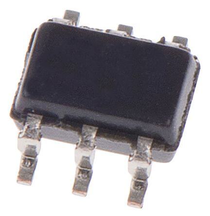
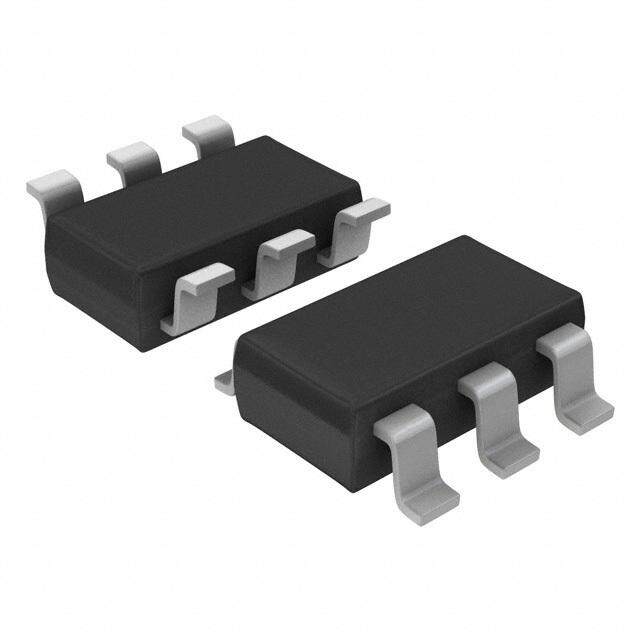
| 供应商器件封装 | SC-70-6 |
| 其它名称 | 296-24170-6 |
| 包装 | Digi-Reel® |
| 同步整流器 | 是 |
| 商标 | Texas Instruments |
| 安装类型 | 表面贴装 |
| 安装风格 | SMD/SMT |
| 封装 | Reel |
| 封装/外壳 | 6-TSSOP,SC-88,SOT-363 |
| 封装/箱体 | SC-70-6 |
| 工作温度 | -40°C ~ 85°C |
| 工作温度范围 | - 40 C to + 85 C |
| 工厂包装数量 | 250 |
| 开关频率 | 2 MHz |
| 拓扑结构 | Boost |
| 最大工作温度 | + 85 C |
| 最大输入电压 | 5.5 V |
| 最小工作温度 | - 40 C |
| 标准包装 | 1 |
| 电压-输入 | 0.7 V ~ 5.5 V |
| 电压-输出 | 1.8 V ~ 5.5 V |
| 电流-输出 | 200mA |
| 类型 | 升压(升压) |
| 系列 | TPS61220 |
| 输出数 | 1 |
| 输出电压 | 1.8 V to 5.5 V |
| 输出电流 | 400 mA |
| 输出端数量 | 1 Output |
| 输出类型 | 可调式 |
| 配用 | /product-detail/zh/TPS61220EVM-319/296-31239-ND/2232831 |
| 频率-开关 | 最高 2MHz |


- 商务部:美国ITC正式对集成电路等产品启动337调查
- 曝三星4nm工艺存在良率问题 高通将骁龙8 Gen1或转产台积电
- 太阳诱电将投资9.5亿元在常州建新厂生产MLCC 预计2023年完工
- 英特尔发布欧洲新工厂建设计划 深化IDM 2.0 战略
- 台积电先进制程称霸业界 有大客户加持明年业绩稳了
- 达到5530亿美元!SIA预计今年全球半导体销售额将创下新高
- 英特尔拟将自动驾驶子公司Mobileye上市 估值或超500亿美元
- 三星加码芯片和SET,合并消费电子和移动部门,撤换高东真等 CEO
- 三星电子宣布重大人事变动 还合并消费电子和移动部门
- 海关总署:前11个月进口集成电路产品价值2.52万亿元 增长14.8%


PDF Datasheet 数据手册内容提取
Product Sample & Technical Tools & Support & Reference Folder Buy Documents Software Community Design TPS61220,TPS61221,TPS61222 SLVS776B–JANUARY2009–REVISEDNOVEMBER2014 TPS6122x Low Input Voltage, 0.7V Boost Converter With 5.5μA Quiescent Current 1 Features 3 Description • Upto95%EfficiencyatTypicalOperating TheTPS6122xfamilydevicesprovideapower-supply 1 solution for products powered by either a single-cell, Conditions two-cell, or three-cell alkaline, NiCd or NiMH, or one- • 5.5 μAQuiescentCurrent cell Li-Ion or Li-polymer battery. Possible output • StartupIntoLoadat0.7VInputVoltage currents depend on the input-to-output voltage ratio. • OperatingInputVoltagefrom0.7Vto5.5V The boost converter is based on a hysteretic controller topology using synchronous rectification to • Pass-ThroughFunctionduringShutdown obtain maximum efficiency at minimal quiescent • MinimumSwitchingCurrent200mA currents. The output voltage of the adjustable version • Protections: can be programmed by an external resistor divider, or is set internally to a fixed output voltage. The – OutputOvervoltage converter can be switched off by a featured enable – Overtemperature pin. While being switched off, battery drain is – InputUndervoltageLockout minimized. The device is offered in a 6-pin SC-70 package (DCK) measuring 2 mm x 2 mm to enable • AdjustableOutputVoltagefrom1.8Vto6V smallcircuitlayoutsize. • FixedOutputVoltageVersions • Small6-pinSC-70Package DeviceInformation(1) PARTNUMBER PACKAGE BODYSIZE(NOM) 2 Applications TPS61220 • BatteryPoweredApplications TPS61221 SC-70(6) 2.00mmx1.25mm – 1to3CellAlkaline,NiCdorNiMH TPS61222 – 1cellLi-IonorLi-Primary (1) For all available packages, see the orderable addendum at theendofthisdocument. • SolarorFuelCellPoweredApplications • ConsumerandPortableMedicalProducts • PersonalCareProducts • WhiteorStatusLEDs • Smartphones 4 Simplified Schematic L VIN 4.71µH LVIN VOUFTB R1 C102µF V1.O8U VT to 6 V Efficiency vs O≥u7tp0%ut Current and Input Voltage (VOUT0.=8 3.3V) 0.7 V to VOUT 10µCF1 EGNND R2 ≥80% 11..83 oltage - V V TPS61220 ut 2.3 p n ≥90% 2.8 V- IIN 0.01 0.1 1 10 100 I - Output Current - mA OUT 1 An IMPORTANT NOTICE at the end of this data sheet addresses availability, warranty, changes, use in safety-critical applications, intellectualpropertymattersandotherimportantdisclaimers.PRODUCTIONDATA.
TPS61220,TPS61221,TPS61222 SLVS776B–JANUARY2009–REVISEDNOVEMBER2014 www.ti.com Table of Contents 1 Features.................................................................. 1 11.1 ApplicationInformation..........................................13 2 Applications........................................................... 1 11.2 TypicalApplications..............................................13 3 Description............................................................. 1 12 PowerSupplyRecommendations..................... 17 4 SimplifiedSchematic............................................. 1 12.1 TypicalPowerSources.........................................17 12.2 InputVoltageEffectsOnOutputCurrentand 5 RevisionHistory..................................................... 2 Efficiency..................................................................17 6 DeviceComparison............................................... 3 12.3 BehaviorWhileDisabled.......................................17 7 PinConfigurationandFunctions......................... 3 12.4 Startup...................................................................17 8 Specifications......................................................... 3 13 Layout................................................................... 18 8.1 AbsoluteMaximumRatings......................................3 13.1 LayoutGuidelines.................................................18 8.2 HandlingRatings.......................................................3 13.2 LayoutExample....................................................18 8.3 RecommendedOperatingConditions.......................4 13.3 ThermalConsiderations........................................18 8.4 ThermalInformation..................................................4 14 DeviceandDocumentationSupport................. 19 8.5 ElectricalCharacteristics...........................................4 14.1 DeviceSupport......................................................19 8.6 TypicalCharacteristics..............................................5 14.2 DocumentationSupport........................................19 9 ParameterMeasurementInformation................10 14.3 RelatedLinks........................................................19 10 DetailedDescription........................................... 11 14.4 Trademarks...........................................................19 10.1 Overview...............................................................11 14.5 ElectrostaticDischargeCaution............................19 10.2 FunctionalBlockDiagrams...................................11 14.6 Glossary................................................................19 10.3 FeatureDescription...............................................11 15 Mechanical,Packaging,andOrderable 10.4 DeviceFunctionalModes......................................12 Information........................................................... 20 11 ApplicationsandImplementation...................... 13 5 Revision History NOTE:Pagenumbersforpreviousrevisionsmaydifferfrompagenumbersinthecurrentversion. ChangesfromRevisionA(April2014)toRevisionB Page • ChangedformatofHandlingRatingstable. .......................................................................................................................... 3 • AddednewnotetoApplicationandImplementationsection................................................................................................ 13 • Renamed"ThermalInformation"sectionto"ThermalConsiderations"section. ................................................................. 18 ChangesfromOriginal(August2009)toRevisionA Page • Updateddatasheetformat..................................................................................................................................................... 1 • ChangedthedatasheettitleFrom:LOWINPUTVOLTAGESTEP-UPCONVERTERIN6PINSC-70PACKAGE To:TPS6122xLOWINPUTVOLTAGE,0.7VBOOSTCONVERTERWITH5.5μAQUIESCENTCURRENT..................... 1 • ChangedFeaturebulletandSimplifiedSchematictextfrom"....1.8Vto5.5V"to"....1.8Vto6V"..................................... 1 • Deleted"machinemodel"ESDratingbecauseJEDECdiscontinueditsusein2012. ......................................................... 3 • ChangedOvervoltageprotectthresholdminandV maxlevelsfrom5.5Vto6V.............................................................. 4 OUT • ChangedAdjustableoutputvoltageversiondescriptiontextstringfrom"....voltageis5.5V"to"....voltageis6.0V"........16 • ChangedLayoutdiagramtocorrecttypoinresistornumbers............................................................................................. 18 2 SubmitDocumentationFeedback Copyright©2009–2014,TexasInstrumentsIncorporated ProductFolderLinks:TPS61220 TPS61221 TPS61222
TPS61220,TPS61221,TPS61222 www.ti.com SLVS776B–JANUARY2009–REVISEDNOVEMBER2014 6 Device Comparison (1) T OUTPUTVOLTAGE PACKAGE PACKAGE(1) PARTNUMBER(2) A DC/DC MARKING Adjustable CKR TPS61220DCK –40°Cto85°C 3.3V CKS 6-pinSC-70 TPS61221DCK 5.0V CKT TPS61222DCK (1) Contactthefactorytocheckavailabilityofotherfixedoutputvoltageversions. (1) Forthemostcurrentpackageandorderinginformation,seethePackageOptionAddendumattheendofthisdocument,orseetheTI websiteatwww.ti.com. (2) TheDCKpackageisavailabletapedandreeled.AddRsuffixtodevicetype(e.g.,TPS61220DCKR)toorderquantitiesof3000devices perreel.Itisalsoavailableinminireels.AddaTsuffixtothedevicetype(i.e.TPS61220DCKT)toorderquantitiesof250devicesper reel. 7 Pin Configuration and Functions DCK PACKAGE (TOPVIEW) VIN EN FB L GND VOUT PinFunctions PIN I/O DESCRIPTION NAME NO. EN 6 I Enableinput(1:enabled,0:disabled).Mustbeactivelytiedhighorlow.Donotleavefloating. FB 2 I Voltagefeedbackofadjustableversion.MustbeconnectedtoV atfixedoutputvoltageversions. OUT GND 3 Control/logicandpowerground L 5 I ConnectionforInductor VIN 1 I Boostconverterinputvoltage VOUT 4 O Boostconverteroutputvoltage 8 Specifications 8.1 Absolute Maximum Ratings overoperatingfree-airtemperaturerange(unlessotherwisenoted)(1) TPS6122x UNIT V InputvoltageonVIN,L,VOUT,EN,FB –0.3to7.5 V IN T Operatingjunctiontemperature –40to150 °C J (1) StressesbeyondthoselistedunderAbsoluteMaximumRatingsmaycausepermanentdamagetothedevice.Thesearestressratings only,andfunctionaloperationofthedeviceattheseoranyotherconditionsbeyondthoseindicatedunderRecommendedOperating Conditionsisnotimplied.Exposuretoabsolute-maximum-ratedconditionsforextendedperiodsmayaffectdevicereliability. 8.2 Handling Ratings MIN MAX UNIT T Storagetemperaturerange –65 150 °C stg Humanbodymodel(HBM),perANSI/ESDA/JEDECJS- Electrostatic 001,allpins(1) –2 2 kV V (ESD) discharge Chargeddevicemodel(CDM),perJEDECspecification JESD22-C101,allpins(2) –1.5 1.5 kV (1) JEDECdocumentJEP155statesthat500VHBMratingallowssafemanufacturingwithastandardESDcontrolprocess. (2) JEDECdocumentJEP157statesthat250VCDMratingallowssafemanufacturingwithastandardESDcontrolprocess. Copyright©2009–2014,TexasInstrumentsIncorporated SubmitDocumentationFeedback 3 ProductFolderLinks:TPS61220 TPS61221 TPS61222
TPS61220,TPS61221,TPS61222 SLVS776B–JANUARY2009–REVISEDNOVEMBER2014 www.ti.com 8.3 Recommended Operating Conditions MIN NOM MAX UNIT V SupplyvoltageatVIN 0.7 5.5 V IN T Operatingvirtualjunctiontemperature –40 125 °C J 8.4 Thermal Information TPS6122x THERMALMETRIC(1) DCK UNIT 6PINS R Junction-to-ambientthermalresistance 231.2 θJA R Junction-to-case(top)thermalresistance 61.8 θJCtop R Junction-to-boardthermalresistance 78.8 θJB °C/W ψ Junction-to-topcharacterizationparameter 2.2 JT ψ Junction-to-boardcharacterizationparameter 78.0 JB R Junction-to-case(bottom)thermalresistance n/a θJCbot (1) Formoreinformationabouttraditionalandnewthermalmetrics,seetheICPackageThermalMetricsapplicationreport,SPRA953. 8.5 Electrical Characteristics overrecommendedfree-airtemperaturerangeandoverrecommendedinputvoltagerange(typicalatanambienttemperature rangeof25°C)(unlessotherwisenoted) PARAMETER TESTCONDITIONS MIN TYP MAX UNIT DC/DCSTAGE V Inputvoltage 0.7 5.5 V IN V Minimuminputvoltageatstartup R ≥150Ω 0.7 V IN Load V TPS61220outputvoltage V <V 1.8 6.0 V OUT IN OUT V TPS61220feedbackvoltage 483 500 513 mV FB V TPS61221outputvoltage(3.3V) V <V 3.20 3.30 3.41 V OUT IN OUT V TPS61222outputvoltage(5V) V <V 4.82 5.00 5.13 V OUT IN OUT I Inductorcurrentripple 200 mA LH V =3.3V,V =1.2V,T =25°C 240 400 mA OUT IN A I switchcurrentlimit SW V =3.3V 200 400 mA OUT V =3.3V 1000 mΩ OUT R Rectifyingswitchonresistance DSon_HSD V =5.0V 700 mΩ OUT V =3.3V 600 mΩ OUT R Mainswitchonresistance DSon_LSD V =5.0V 550 mΩ OUT Lineregulation V <V 0.5% IN OUT Loadregulation V <V 0.5% IN OUT V 0.5 0.9 μA IN I Quiescentcurrent I =0mA,V =V =1.2V,V =3.3V Q O EN IN OUT V 5 7.5 μA OUT I Shutdowncurrent V V =0V,V =1.2V,V ≥V 0.2 0.5 μA SD IN EN IN OUT IN I LeakagecurrentintoVOUT V =0V,V =1.2V,V =3.3V 1 μA LKG_VOUT EN IN OUT I LeakagecurrentintoL V =0V,V =1.2V,V =1.2V,V ≥V 0.01 0.2 μA LKG_L EN IN L OUT IN I TPS61220Feedbackinputcurrent V =0.5V 0.01 μA FB FB I ENinputcurrent ClampedonGNDorV (V <1.5V) 0.005 0.1 μA EN IN IN CONTROLSTAGE V ENinputlowvoltage V ≤1.5V 0.2×V V IL IN IN V ENinputhighvoltage V ≤1.5V 0.8×V V IH IN IN V ENinputlowvoltage 5V>V >1.5V 0.4 V IL IN V ENinputhighvoltage 5V>V >1.5V 1.2 V IH IN 4 SubmitDocumentationFeedback Copyright©2009–2014,TexasInstrumentsIncorporated ProductFolderLinks:TPS61220 TPS61221 TPS61222
TPS61220,TPS61221,TPS61222 www.ti.com SLVS776B–JANUARY2009–REVISEDNOVEMBER2014 Electrical Characteristics (continued) overrecommendedfree-airtemperaturerangeandoverrecommendedinputvoltagerange(typicalatanambienttemperature rangeof25°C)(unlessotherwisenoted) PARAMETER TESTCONDITIONS MIN TYP MAX UNIT V Undervoltagelockoutthresholdfor V decreasing 0.5 0.7 V UVLO IN turnoff Overvoltageprotectionthreshold 6.0 7.5 V Overtemperatureprotection 140 °C Overtemperaturehysteresis 20 °C 8.6 Typical Characteristics TABLEOFGRAPHS FIGURE MaximumOutputCurrent versusInputVoltage(TPS61220,TPS61221,TPS61222) Figure1 versusOutputCurrent,V =1.8V,V =[0.7V;1.2V;1.5V](TPS61220) Figure2 OUT IN versusOutputCurrent,V =[0.7V;1.2V;2.4V;3V](TPS61221) Figure3 IN versusOutputCurrent,V =[0.7V;1.2V;2.4V;3.6V;4.2V](TPS61222) Figure4 IN Efficiency versusInputVoltage,V =1.8V,I =[100µA;1mA;10mA;50mA] OUT OUT Figure5 (TPS61220) versusInputVoltage,I =[100µA;1mA;10mA;50mA](TPS61221) Figure6 OUT versusInputVoltage,I =[100µA;1mA;10mA;50mA](TPS61222) Figure7 OUT InputCurrent atNoOutputLoad,DeviceEnabled(TPS61220,TPS61221,TPS61222) Figure8 versusOutputCurrent,V =1.8V,V =[0.7V;1.2V](TPS61220) Figure9 OUT IN versusOutputCurrent,V =[0.7V;1.2V;2.4V](TPS61221) Figure10 IN OutputVoltage versusOutputCurrent,V =[0.7V;1.2V;2.4V;3.6V](TPS61222) Figure11 IN versusInputVoltage,DeviceDisabled,R =[1kΩ;10kΩ](TPS6122x) Figure12 LOAD OutputVoltageRipple,V =0.8V,V =1.8V,I =20mA(TPS61220) Figure13 IN OUT OUT OutputVoltageRippleV =1.8V,I =50mA(TPS61221) Figure14 IN OUT LoadTransientResponse,V =1.2V,I =6mAto50mA(TPS61221) Figure15 IN OUT LoadTransientResponse,V =2.4V,I =14mAto126mA(TPS61222) Figure16 IN OUT LineTransientResponse,V =1.8Vto2.4V,R =100Ω(TPS61221) Figure17 IN LOAD Waveforms LineTransientResponse,VIN=2.8Vto3.6V,RLOAD=100Ω(TPS61222) Figure18 StartupafterEnable,V =0.7V,V =1.8V,R =150Ω(TPS61220) Figure19 IN OUT LOAD StartupafterEnable,V =0.7V,R =150Ω,(TPS61222) Figure20 IN LOAD ContinuousCurrentOperation,V =1.2V,V =1.8V,I =50mA IN OUT OUT Figure21 (TPS61220) DiscontinuousCurrentOperation,V =1.2V,V =1.8V,I =10mA IN OUT OUT Figure22 (TPS61220) Copyright©2009–2014,TexasInstrumentsIncorporated SubmitDocumentationFeedback 5 ProductFolderLinks:TPS61220 TPS61221 TPS61222
TPS61220,TPS61221,TPS61222 SLVS776B–JANUARY2009–REVISEDNOVEMBER2014 www.ti.com 300 100 90 250 A 80 m Maximum output Current - 21105500000 TPS61221 VO= 3.3 V TPS61222 VO= 5 V - Efficiency - %h 234567000000 VI= 0.7 V VI= 1.2 V VI= 1.5 V TPS61220 VO= 1.8 V 10 0 0 0.7 1.2 1.7 2.2 2.7 3.2 3.7 4.2 4.7 0.01 0.1 1 10 100 VI- Input Voltage - V IO- Output Current - mA V =1.8V O Figure1.MaximumOutputCurrentversusInputVoltage Figure2.EfficiencyversusOutputCurrentandInput (TPS61220,TPS61221,TPS61222) Voltage(TPS61220) 100 100 90 90 80 80 70 70 % VI= 3 V % - Efficiency - h 456000 VI= 0.7 V VI= 1.2 V VI= 2.4 V - Efficiency - h 456000 VI= 0.7 V VI= 1.2 VVI= 2.4 V VI= 3.6 V VI= 4.2 V 30 30 20 20 10 10 0 0 0.01 0.1 1 10 100 0.01 0.1 1 10 100 IO- Output Current - mA IO- Output Current - mA V =3.3V V =5V O O Figure3.EfficiencyversusOutputCurrentandInput Figure4.EfficiencyversusOutputCurrentandInput Voltage(TPS61221) Voltage(TPS61222) 100 100 90 IO= 10 mA 90 IO= 10 mA 80 80 Efficiency - % 45670000 IO= 50 mA IO= 100mA IO= 1 mA Efficiency - % 45670000 IO= 50 mA IO= 1 mA IO= 100mA - - h h 30 30 20 20 10 10 0 0 0.7 0.9 1.1 1.3 1.5 1.7 0.7 1.2 1.7 2.2 2.7 3.2 VI- Input Voltage - V VI- Input Voltage - V VO=1.8V VO=3.3V Figure5.EfficiencyversusInputVoltageandOutput Figure6.EfficiencyversusInputVoltageandOutput Current(TPS61220) Current(TPS61221) 6 SubmitDocumentationFeedback Copyright©2009–2014,TexasInstrumentsIncorporated ProductFolderLinks:TPS61220 TPS61221 TPS61222
TPS61220,TPS61221,TPS61222 www.ti.com SLVS776B–JANUARY2009–REVISEDNOVEMBER2014 100 80 70 80 IO= 10 mA IO= 50 mA 60 - Efficiency - %h 4600 IO= 100mAIO= 1 mA - Input Current -Am 345000 TPS61222T, PVSO6=1 2 52 1VT, PVSO6=1 232.30 ,V VO= 1.8 V II 20 20 10 0 0 0.7 1.7 2.7 3.7 4.7 0.7 1.7 2.7 3.7 4.7 VI- Input Voltage - V VI- Input Voltage - V V =5V Deviceenabled O Figure7.EfficiencyversusInputVoltageandOutput Figure8.NoLoadInputCurrentversusInputVoltage, Current(TPS61222) DeviceEnabled(TPS61220,TPS61221,TPS61222) 1.9 3.5 1.85 3.4 ge - V VI= 1.2 V ge - V VI= 2.4 V ut Volta 1.8 ut Volta 3.3 p p Out Out VI= 0.7 V - O VI= 0.7 V - O V1.75 V 3.2 VI= 1.2 V 1.7 3.1 0.01 0.1 1 10 100 0.01 0.1 1 10 100 IO- Output Current - mA IO- Output Current - mA V =1.8V V =3.3V O O Figure9.OutputVoltageversusOutputCurrentandInput Figure10.OutputVoltageversusOutputCurrentandInput Voltage(TPS61220) Voltage(TPS61221) 5.2 4.5 4 5.1 V 3.5 - Output Voltage - V 5 VI=V I2=.4 1 V.2 V VI= 3.6 V V- Output Voltage - O12..5523 RLOAD= 10 kW O V 4.9 VI= 0.7 V 1 RLOAD= 1 kW 0.5 4.8 0 0.01 0.1 1 10 100 0.7 1.2 1.7 2.2 2.7 3.2 3.7 4.2 4.7 5.2 IO- Output Current - mA VI- Input Voltage - V V =5V V =0V O EN Figure11.OutputVoltageversusOutputCurrentandInput Figure12.OutputVoltageversusInputVoltage,Device Voltage(TPS61222) Disabled(TPS61220) Copyright©2009–2014,TexasInstrumentsIncorporated SubmitDocumentationFeedback 7 ProductFolderLinks:TPS61220 TPS61221 TPS61222
TPS61220,TPS61221,TPS61222 SLVS776B–JANUARY2009–REVISEDNOVEMBER2014 www.ti.com Icoil Icoil 50 mA/div 50 mA/div Offset: 0 V Offset: 0A VO VO 10 mA/div 10 mV/div Offset: 3.31 V Offset: 1.8 V 1ms/div 1ms/div V =0.8V V =1.8V I =20mA V =1.8V V =3.3V I =50mA I O O I O O Figure13.OutputVoltageRipple(TPS61220) Figure14.OutputVoltageRipple(TPS61221) Offset: 0A IL Offset: 0A IL 200 mA/div 200 mA/div IO 50 mA/div Offset: 0A IO Offset: 0A 20 mA/div VO Offset: 3.31 V 50 mV/div VO Offset: 5 V 50 mV/div 200ms/div 200ms/div VI=1.2V IO=6mAto50mA VI=2.4V IO=14mAto126mA Figure15. LoadTransientResponse(TPS61221) Figure16. LoadTransientResponse(TPS61222) VI VI 200 mV/div 200 mV/div Offset: 1.8 V Offset: 2.8 V VO VO 20 mV/div Offset: 3.3 V 20 mV/div VI1.8 to 2.4 V, RLOAD= 100W, trise= tfall= 20 ms Offset: 5 V 200ms/div 200ms/div VI=2.4Vto2.4V RLOAD=100Ω trise=tfall=20ms VI=2.8Vto3.6V RLOAD=100Ω trise=tfall=20ms Figure17. LineTransientResponse(TPS61221) Figure18. LineTransientResponse(TPS61222) 8 SubmitDocumentationFeedback Copyright©2009–2014,TexasInstrumentsIncorporated ProductFolderLinks:TPS61220 TPS61221 TPS61222
TPS61220,TPS61221,TPS61222 www.ti.com SLVS776B–JANUARY2009–REVISEDNOVEMBER2014 Offset: 0 V VEN Offset: 0 V VEN 500 mV/div 500 mV/div Offset: 0A Icoil Offset: 0A Icoil 100 mA/div 100 mA/div VL Offset: 0 V VL Offset: 0 V 1 V/div 2 V/div VO Offset: 0 V VO Offset: 0 V 1 V/div 2 V/div 500ms/div 500ms/div VI=0.7V VO=1.8V RLOAD=150Ω VI=0.7V VO=3.3V RLOAD=50Ω Figure19.StartupAfterEnable(TPS61120) Figure20. StartupAfterEnable(TPS61221) Icoil Icoil 100 mA/div 100 mA/div Offset: 0A Offset: 0A VL VL 2 V/div 2 V/div Offset: 0 V Offset: 0 V VO VO 10 mV/div 10 mV/div Offset: 1.8 V Offset: 1.8 V 1ms/div 1ms/div V =1.2V V =1.8V I =50mA V =1.2V V =1.8V I =10mA I O O I O O Figure21. ContinuousCurrentOperation(TPS61220) Figure22. DiscontinuousCurrentOperation(TPS61220) Copyright©2009–2014,TexasInstrumentsIncorporated SubmitDocumentationFeedback 9 ProductFolderLinks:TPS61220 TPS61221 TPS61222
TPS61220,TPS61221,TPS61222 SLVS776B–JANUARY2009–REVISEDNOVEMBER2014 www.ti.com 9 Parameter Measurement Information L 1 L VOUT V OUT R 1 V VIN FB C IN R 2 EN 2 C 1 GND TPS6122x Table1.ListOfComponents: COMPONENT PARTNUMBER MANUFACTURER VALUE REFERENCE C GRM188R60J106ME84D Murata 10μF,6.3V.X5RCeramic 1 C GRM188R60J106ME84D Murata 10μF,6.3V.X5RCeramic 2 L EPL3015-472MLB Coilcraft 4.7μH 1 adjustableversion:Valuesdependingonthe R ,R programmedoutputvoltage 1 2 fixedversion:R =0Ω,R notused 1 2 10 SubmitDocumentationFeedback Copyright©2009–2014,TexasInstrumentsIncorporated ProductFolderLinks:TPS61220 TPS61221 TPS61222
TPS61220,TPS61221,TPS61222 www.ti.com SLVS776B–JANUARY2009–REVISEDNOVEMBER2014 10 Detailed Description 10.1 Overview The TPS6122x is a high performance, high efficient family of switching boost converters. To achieve high efficiency, the power stage is realized as a synchronous-boost topology. For the power switching, two actively- controlledlow-R powerMOSFETsareimplemented. DSon 10.2 Functional Block Diagrams L VOUT L VOUT VOUT VOUT VIN VIN Gate Gate Driver Driver VIN Start Up VIN Start Up Current Current Sensor Sensor FB EN CCDDooeennvvttiicrcrooeell FB EN CCDDooeennvvttiicrcrooeell GND VREF GND VREF Figure23.FunctionalBlockDiagram(Adjustable Figure24.FunctionalBlockDiagram(FixedOutput Version) VoltageVersion) 10.3 Feature Description 10.3.1 ControllerCircuit The device is controlled by a hysteretic current mode controller. This controller regulates the output voltage by keeping the inductor ripple current constant in the range of 200 mA and adjusting the offset of this inductor current depending on the output load. If the required average input current is lower than the average inductor current defined by this constant ripple current, the inductor current becomes discontinuous to keep the efficiency highunderlow-loadconditions. I L Continuous Current Operation Discontinuous Current Operation 200 mA (typ.) 200 mA (typ.) t Figure25. HystereticCurrentOperation The output voltage V is monitored via the feedback network which is connected to the voltage error amplifier. OUT To regulate the output voltage, the voltage error amplifier compares this feedback voltage to the internal voltage reference and adjusts the required offset of the inductor current accordingly. In fixed output voltage devices, an internal feedback network is used to program the output voltage. In adjustable versions an external resistor dividerisrequired. The self-oscillating hysteretic current mode architecture is inherently stable and allows fast response to load variations.Thisarchitecturealsoallowsusingawiderangeofinductorandcapacitorvalues. Copyright©2009–2014,TexasInstrumentsIncorporated SubmitDocumentationFeedback 11 ProductFolderLinks:TPS61220 TPS61221 TPS61222
TPS61220,TPS61221,TPS61222 SLVS776B–JANUARY2009–REVISEDNOVEMBER2014 www.ti.com Feature Description (continued) 10.3.2 DeviceEnableAndShutdownMode The device is enabled when EN is driven high, and shut down when EN is low. During shutdown, the converter stops switching and all internal control circuitry is turned off. During shutdown, the input voltage is connected to the output through the back-gate diode of the rectifying MOSFET. This means that voltage is always present at theoutput,whichcanbeashighastheinputvoltageorlowerdependingontheload. 10.3.3 Startup After the EN pin is tied high, the device begins to operate. If the input voltage is not high enough to supply the control circuit properly, a startup oscillator operates the switches. During this phase, the switching frequency is controlled by the oscillator, and the maximum switch current is limited. When the device has built up the output voltage to approximately 1.8V, high enough to supply the control circuit, the device switches to its normal hystereticcurrentmodeoperation.Thestartuptimedependsoninputvoltageandloadcurrent. 10.3.4 OperationAtOutputOverload If, in normal boost operation, the inductor current reaches the internal switch current limit threshold, the main switch is turned off to stop further increase of the input current. In this case the output voltage will decrease becausethedevicecannotprovidesufficientpowertomaintainthesetoutputvoltage. If the output voltage drops below the input voltage, the backgate diode of the rectifying switch becomes forward biased, and current starts to flow through it. This diode cannot be turned off, so the current finally is only limited bytheremainingDCresistances.Assoonastheoverloadconditionisremoved,theconverterresumesproviding thesetoutputvoltage. 10.3.5 UndervoltageLockout An undervoltage lockout function stops the operation of the converter if the input voltage drops below the typical undervoltagelockoutthreshold.Thisfunctionisimplementedinordertopreventconvertermalfunction. 10.3.6 OvervoltageProtection If, for any reason, the output voltage is not fed back properly to the input of the voltage amplifier, control of the output voltage is lost. Therefore an overvoltage protection is implemented to avoid the output voltage exceeding critical values for the device and possibly for the system it is supplying. For this protection, the TPS6122x output voltage is also monitored internally. If it reaches the internally programmed threshold of 6.5 V, typically the voltageamplifierregulates(limits)theoutputvoltagetothisvalue. IftheTPS6122xisusedtodriveLEDs,thisfeatureprotectsthecircuitiftheLEDfails. 10.3.7 OvertemperatureProtection The device has a built-in temperature sensor which monitors the internal IC junction temperature. If the temperature exceeds the programmed threshold (see electrical characteristics table), the device stops operating. As soon as the IC temperature has decreased below the programmed threshold, it starts operating again. To preventunstableoperationclosetotheregionofovertemperaturethreshold,abuilt-inhysteresisisimplemented. 10.4 Device Functional Modes • Enabledordisabled • Continuousordiscontinuouscurrentoperation • Protectivemechanisms – OutputOverload – Undervoltage – Overvoltage – Overtemperature 12 SubmitDocumentationFeedback Copyright©2009–2014,TexasInstrumentsIncorporated ProductFolderLinks:TPS61220 TPS61221 TPS61222
TPS61220,TPS61221,TPS61222 www.ti.com SLVS776B–JANUARY2009–REVISEDNOVEMBER2014 11 Applications and Implementation NOTE Information in the following applications sections is not part of the TI component specification, and TI does not warrant its accuracy or completeness. TI’s customers are responsible for determining suitability of components for their purposes. Customers should validateandtesttheirdesignimplementationtoconfirmsystemfunctionality. 11.1 Application Information The TPS6122x family devices provide a power-supply solution for products powered by either a single-cell, two- cell, or three-cell alkaline, NiCd or NiMH, or one-cell Li-Ion or Li-polymer battery. Use the following design procedure to select component values for the TPS61220 device and the TPS61222 device. Alternatively, use the SwitcherPro™tool.Thissectionpresentsasimplifieddiscussionofthedesignprocess. 11.2 Typical Applications 11.2.1 SpecificApplication,FixedOutputVoltageSupply L 1 L VOUT VOUT V VIN FB C IN 2 EN C 1 GND TPS6122x fixed output voltage Figure26. TypicalApplicationCircuitForFixedOutputVoltageOption 11.2.1.1 DesignRequirements • Single5Voutputatupto60mA • Powersource,twoAAalkalinecells • Greaterthan90%conversionefficiency 11.2.1.2 DetailedDesignProcedure 11.2.1.2.1 DeviceChoice The TPS61222 DC/DC converter is intended for systems powered by anything from a single cell through up to three Alkaline, NiCd or NiMH cells with a total typical pin voltage between 0.7 V and 5.5 V. They can also be used in systems powered by one-cell Li-Ion or Li-Polymer batteries with a typical voltage between 2.5 V and 4.2 V. Additionally, any other voltage source with a typical output voltage between 0.7 V and 5.5 V can be used with theTPS61222. 11.2.1.2.2 ProgrammingTheOutputVoltage In the fixed-voltage version used for this example, the output voltage is set by an internal resistor divider. The FB pin is used to sense the output voltage. To configure the device properly, connect the FB pin directly to VOUT as showninFigure26. 11.2.1.2.3 InductorSelection To make sure that the device can operate, a suitable inductor must be connected between pin VIN and pin L. Inductorvaluesof4.7μHshowgoodperformanceoverthewholeinputandoutputvoltagerange. Choosingotherinductancevaluesaffectstheswitchingfrequencyfproportionalto1/LasshowninEquation1. Copyright©2009–2014,TexasInstrumentsIncorporated SubmitDocumentationFeedback 13 ProductFolderLinks:TPS61220 TPS61221 TPS61222
TPS61220,TPS61221,TPS61222 SLVS776B–JANUARY2009–REVISEDNOVEMBER2014 www.ti.com Typical Applications (continued) 1 V ´(V -V ) L= ´ IN OUT IN f´200 mA V OUT (1) Choosing inductor values higher than 4.7 μH can improve efficiency due to reduced switching frequency and thereforewithreducedswitchinglosses.Usinginductorvaluesbelow2.2 μHisnotrecommended. Having selected an inductance value, the peak current for the inductor in steady-state operation can be calculated.Equation2 givesthepeak-currentestimate. ì V ´ I ï OUT OUT +100mA; continouscurrentoperation I = í 0.8´V L,MAX IN ï î200mA; discontinuouscurrentoperation (2) Equation 2 provides a suitable inductor current rating. However, remember that load transients and error conditionsmaycausehigherinductorcurrents. Equation 3 provides an easy way to estimate whether the device will work in continuous or discontinuous operation depending on the operating points. As long as the Equation 3 is true, continuous operation is typically established.IfEquation3 becomesfalse,discontinousoperationistypicallyestablished. V ´I OUT OUT >0.8´100 mA V IN (3) ThefollowinginductorseriesfromdifferentsuppliershavebeenusedwithTPS6122xconverters: Table2.ListOfInductors VENDOR INDUCTORSERIES EPL3015 Coilcraft EPL2010 Murata LQH3NP TajoYuden NR3015 WurthElektronik WE-TPCTypS 11.2.1.2.4 CapacitorSelection 11.2.1.2.4.1 InputCapacitor An input capacitor value of at least 10 μF is recommended to improve transient behavior of the regulator and EMI behavior of the total power supply circuit. A ceramic capacitor placed as close as possible to the VIN and GNDpinsoftheICisrecommended. 11.2.1.2.4.2 OutputCapacitor For the output capacitor C , small ceramic capacitors are recommended, placed as close as possible to the 2 VOUT and GND pins of the IC. If, for any reason, the application requires the use of large capacitors which cannot be placed close to the IC, the use of a small ceramic capacitor with a capacitance value of around 2.2μF in parallel to the large one is recommended. This small capacitor should be placed as close as possible to the VOUTandGNDpinsoftheIC. A minimum capacitance value of 4.7 μF should be used, 10 μF is recommended. If the inductor value exceeds 4.7 μH, the value of the output capacitance value needs to be half the inductance value or higher for stability reasons,seeEquation4. L C ³ ´ 2 2 (4) 14 SubmitDocumentationFeedback Copyright©2009–2014,TexasInstrumentsIncorporated ProductFolderLinks:TPS61220 TPS61221 TPS61222
TPS61220,TPS61221,TPS61222 www.ti.com SLVS776B–JANUARY2009–REVISEDNOVEMBER2014 The TPS6122x is not sensitive to the ESR in terms of stability. However, low ESR capacitors, such as ceramic capacitors, are recommended anyway to minimize output voltage ripple. If heavy load changes are expected, increasetheoutputcapacitorvaluetoavoidoutputvoltagedropsduringfastloadtransients. 11.2.1.3 ApplicationCurves Figure 27 shows the excellent efficiency of the converter, which remains above 80% even with heavily dischargedcells. 100 80 IO= 10 mA IO= 50 mA % y - 60 IO= 1 mA c en IO= 100mA ci Effi - 40 h 20 0 0.7 1.7 2.7 3.7 4.7 VI- Input Voltage - V Figure27.TPS61222Performance 11.2.2 SpecificApplication,VariableOutputVoltageSupply L 1 L VOUT V OUT R 1 V VIN FB C IN R 2 EN 2 C 1 GND TPS6122x Figure28. ApplicationCircuitForAdjustableOutputVoltageOption 11.2.2.1 DesignRequirements • Single4.2Voutputatupto50mA • Powersource,twoAAalkalinecells • Greaterthan80%conversionefficiency 11.2.2.2 DetailedDesignProcedure The design procedure for this application is identical to that for the fixed-output supply except for programming theoutputvoltage. 11.2.2.2.1 DeviceSelection ThisapplicationexampleusestheTPS61220sothattheoutputvoltagecanbesetat4.2V. Copyright©2009–2014,TexasInstrumentsIncorporated SubmitDocumentationFeedback 15 ProductFolderLinks:TPS61220 TPS61221 TPS61222
TPS61220,TPS61221,TPS61222 SLVS776B–JANUARY2009–REVISEDNOVEMBER2014 www.ti.com 11.2.2.2.2 ProgrammingTheOutputVoltage In the adjustable output versions, an external resistor divider is used to adjust the output voltage. The resistor divider must be connected between VOUT, FB and GND as shown in Figure 28. When the output voltage is regulated properly, the typical voltage value at the FB pin is 500 mV for the adjustable devices. The maximum recommended value for the output voltage is 6.0 V. The current through the resistor divider should be about 100 times greater than the current into the FB pin. The typical current into the FB pin is 0.01 μA, and the voltage acrosstheresistorbetweenFBandGND,R ,istypically500mV.Basedonthosetwovalues,therecommended 2 value for R should be lower than 500 kΩ, in order to set the divider current to 1 μA or higher. The value of the 2 resistor connected between VOUT and FB, R , depending on the needed output voltage (V ), can be 1 OUT calculatedusingEquation5: æV ö R1 = R2 x ç OUT -1÷ V è FB ø (5) For this example, if an output voltage of 4.2 V is needed, a 1.2-MΩ resistor is calculated for R when 160 kΩ is 1 selectedforR .Thiswouldyieldanoutputvoltageof4.25V,neglectingresistortolerances. 2 11.2.2.2.3 InductorSelection SeeInductorSelectionforadiscussiononinductorchoice. 11.2.2.2.4 CapacitorSelection The procedure for selecting capacitors is the same as for the fixed output voltage circuit. See Capacitor Selection. 11.2.2.3 ApplicationCurves Figure 29 shows the excellent efficiency of the converter, which remains above 80% with heavily discharged cells. 100 80 I = 50 mA I = 10 mA O O % y - 60 IO= 1 mA c en IO= 100mA ci Effi - 40 h 20 0 0.7 1.7 2.7 3.7 4.7 V - Input Voltage - V I Figure29.TPS61220Performance 16 SubmitDocumentationFeedback Copyright©2009–2014,TexasInstrumentsIncorporated ProductFolderLinks:TPS61220 TPS61221 TPS61222
TPS61220,TPS61221,TPS61222 www.ti.com SLVS776B–JANUARY2009–REVISEDNOVEMBER2014 12 Power Supply Recommendations 12.1 Typical Power Sources The high conversion efficiency of this device encourages the use of a wide range of battery types. Photovoltaic cells and large capacitors ('supercapacitors') may also serve as power sources within the limits specified in RecommendedOperatingConditions. 12.2 Input Voltage Effects On Output Current and Efficiency The TPS6122x devices have a wide input-voltage range, and deliver enough current to be applicable to many portable applications. However, at lower extremes of input voltage, less output current is available, and efficiency is somewhat less. Figure 1 - Figure 11 show the tradeoffs between input voltage, output current capacity and conversion efficiency, and allow the designer to plan how far to discharge a battery array before system shutdownoccurs. 12.3 Behavior While Disabled Whenthedeviceisdisabled,theoutputvoltagefollowsthepower-sourcevoltageasshowninFigure12. 12.4 Startup SeethedescriptionoftheStartupsequenceformoreinformation. Copyright©2009–2014,TexasInstrumentsIncorporated SubmitDocumentationFeedback 17 ProductFolderLinks:TPS61220 TPS61221 TPS61222
TPS61220,TPS61221,TPS61222 SLVS776B–JANUARY2009–REVISEDNOVEMBER2014 www.ti.com 13 Layout 13.1 Layout Guidelines As for all switching power supplies, the layout is an important step in the design, especially at high peak currents and high switching frequencies. If the layout is not carefully done, the regulator could show stability problems as well as EMI problems. Therefore, use wide and short traces for the main current path and for the power ground paths.Theinputandoutputcapacitor,aswellastheinductorshouldbeplacedascloseaspossibletotheIC. The feedback divider in an application using the TPS61220 should be placed as close as possible to the control ground pin of the IC. To route the ground path from the resistor divider, use short traces as well, separated from the power ground traces. This avoids ground shift problems, which can occur due to superimposition of power groundcurrentandcontrolgroundcurrent.AssurethatthegroundtracesareconnectedclosetothedeviceGND pin. 13.2 Layout Example L1 V V OUT e IN bl a n E C2 C1 GND GND N R2 VI T U O V R1 Figure30. PCBLayoutSuggestionForAdjustableOutputVoltageOptions 13.3 Thermal Considerations Implementation of integrated circuits in low-profile and fine-pitch surface-mount packages typically requires special attention to power dissipation. Many system-dependent issues such as thermal coupling, airflow, added heat sinks and convection surfaces, and the presence of other heat-generating components affect the power- dissipationlimitsofagivencomponent. Threebasicapproachesforenhancingthermalperformancearelistedbelow. • Improvingthepower-dissipationcapabilityofthePCBdesign • ImprovingthethermalcouplingofthecomponenttothePCB • Introducingairflowinthesystem For more details on how to use the thermal parameters in the dissipation ratings table please check the Thermal CharacteristicsApplicationNote(SZZA017) andtheICPackageThermalMetricsApplicationNote(SPRA953). 18 SubmitDocumentationFeedback Copyright©2009–2014,TexasInstrumentsIncorporated ProductFolderLinks:TPS61220 TPS61221 TPS61222
TPS61220,TPS61221,TPS61222 www.ti.com SLVS776B–JANUARY2009–REVISEDNOVEMBER2014 14 Device and Documentation Support 14.1 Device Support 14.1.1 Third-PartyProductsDisclaimer TI'S PUBLICATION OF INFORMATION REGARDING THIRD-PARTY PRODUCTS OR SERVICES DOES NOT CONSTITUTE AN ENDORSEMENT REGARDING THE SUITABILITY OF SUCH PRODUCTS OR SERVICES OR A WARRANTY, REPRESENTATION OR ENDORSEMENT OF SUCH PRODUCTS OR SERVICES, EITHER ALONEORINCOMBINATIONWITHANYTIPRODUCTORSERVICE. 14.1.2 DevelopmentSupport TPS61220EVM-319EvaluationModule SwitcherProSwitchingPowerSupplyDesignTool(CircuitDesign & Simulation) 14.2 Documentation Support 14.2.1 RelatedDocumentation GasSensorPlatformReferenceDesign WirelessHeartMonitorwithBluetoothLowEnergy 14.3 Related Links The table below lists quick access links. Categories include technical documents, support and community resources,toolsandsoftware,andquickaccesstosampleorbuy. Table3.RelatedLinks TECHNICAL TOOLS& SUPPORT& PARTS PRODUCTFOLDER SAMPLE&BUY DOCUMENTS SOFTWARE COMMUNITY TPS61220 Clickhere Clickhere Clickhere Clickhere Clickhere TPS61221 Clickhere Clickhere Clickhere Clickhere Clickhere TPS61222 Clickhere Clickhere Clickhere Clickhere Clickhere 14.4 Trademarks SwitcherProisatrademarkofTexasInstruments. Allothertrademarksarethepropertyoftheirrespectiveowners. 14.5 Electrostatic Discharge Caution Thesedeviceshavelimitedbuilt-inESDprotection.Theleadsshouldbeshortedtogetherorthedeviceplacedinconductivefoam duringstorageorhandlingtopreventelectrostaticdamagetotheMOSgates. 14.6 Glossary SLYZ022—TIGlossary. Thisglossarylistsandexplainsterms,acronyms,anddefinitions. Copyright©2009–2014,TexasInstrumentsIncorporated SubmitDocumentationFeedback 19 ProductFolderLinks:TPS61220 TPS61221 TPS61222
TPS61220,TPS61221,TPS61222 SLVS776B–JANUARY2009–REVISEDNOVEMBER2014 www.ti.com 15 Mechanical, Packaging, and Orderable Information The following pages include mechanical packaging and orderable information. This information is the most current data available for the designated devices. This data is subject to change without notice and revision of thisdocument.Forbrowser-basedversionsofthisdatasheet,refertotheleft-handnavigation. 20 SubmitDocumentationFeedback Copyright©2009–2014,TexasInstrumentsIncorporated ProductFolderLinks:TPS61220 TPS61221 TPS61222
PACKAGE OPTION ADDENDUM www.ti.com 6-Feb-2020 PACKAGING INFORMATION Orderable Device Status Package Type Package Pins Package Eco Plan Lead/Ball Finish MSL Peak Temp Op Temp (°C) Device Marking Samples (1) Drawing Qty (2) (6) (3) (4/5) TPS61220DCKR ACTIVE SC70 DCK 6 3000 Green (RoHS NIPDAU Level-1-260C-UNLIM -40 to 85 CKR & no Sb/Br) TPS61220DCKT ACTIVE SC70 DCK 6 250 Green (RoHS NIPDAU Level-1-260C-UNLIM -40 to 85 CKR & no Sb/Br) TPS61221DCKR ACTIVE SC70 DCK 6 3000 Green (RoHS NIPDAU Level-1-260C-UNLIM -40 to 85 CKS & no Sb/Br) TPS61221DCKT ACTIVE SC70 DCK 6 250 Green (RoHS NIPDAU Level-1-260C-UNLIM -40 to 85 CKS & no Sb/Br) TPS61222DCKR ACTIVE SC70 DCK 6 3000 Green (RoHS NIPDAU Level-1-260C-UNLIM -40 to 85 CKT & no Sb/Br) TPS61222DCKT ACTIVE SC70 DCK 6 250 Green (RoHS NIPDAU Level-1-260C-UNLIM -40 to 85 CKT & no Sb/Br) (1) The marketing status values are defined as follows: ACTIVE: Product device recommended for new designs. LIFEBUY: TI has announced that the device will be discontinued, and a lifetime-buy period is in effect. NRND: Not recommended for new designs. Device is in production to support existing customers, but TI does not recommend using this part in a new design. PREVIEW: Device has been announced but is not in production. Samples may or may not be available. OBSOLETE: TI has discontinued the production of the device. (2) RoHS: TI defines "RoHS" to mean semiconductor products that are compliant with the current EU RoHS requirements for all 10 RoHS substances, including the requirement that RoHS substance do not exceed 0.1% by weight in homogeneous materials. Where designed to be soldered at high temperatures, "RoHS" products are suitable for use in specified lead-free processes. TI may reference these types of products as "Pb-Free". RoHS Exempt: TI defines "RoHS Exempt" to mean products that contain lead but are compliant with EU RoHS pursuant to a specific EU RoHS exemption. Green: TI defines "Green" to mean the content of Chlorine (Cl) and Bromine (Br) based flame retardants meet JS709B low halogen requirements of <=1000ppm threshold. Antimony trioxide based flame retardants must also meet the <=1000ppm threshold requirement. (3) MSL, Peak Temp. - The Moisture Sensitivity Level rating according to the JEDEC industry standard classifications, and peak solder temperature. (4) There may be additional marking, which relates to the logo, the lot trace code information, or the environmental category on the device. (5) Multiple Device Markings will be inside parentheses. Only one Device Marking contained in parentheses and separated by a "~" will appear on a device. If a line is indented then it is a continuation of the previous line and the two combined represent the entire Device Marking for that device. Addendum-Page 1
PACKAGE OPTION ADDENDUM www.ti.com 6-Feb-2020 (6) Lead/Ball Finish - Orderable Devices may have multiple material finish options. Finish options are separated by a vertical ruled line. Lead/Ball Finish values may wrap to two lines if the finish value exceeds the maximum column width. Important Information and Disclaimer:The information provided on this page represents TI's knowledge and belief as of the date that it is provided. TI bases its knowledge and belief on information provided by third parties, and makes no representation or warranty as to the accuracy of such information. Efforts are underway to better integrate information from third parties. TI has taken and continues to take reasonable steps to provide representative and accurate information but may not have conducted destructive testing or chemical analysis on incoming materials and chemicals. TI and TI suppliers consider certain information to be proprietary, and thus CAS numbers and other limited information may not be available for release. In no event shall TI's liability arising out of such information exceed the total purchase price of the TI part(s) at issue in this document sold by TI to Customer on an annual basis. OTHER QUALIFIED VERSIONS OF TPS61222 : •Enhanced Product: TPS61222-EP NOTE: Qualified Version Definitions: •Enhanced Product - Supports Defense, Aerospace and Medical Applications Addendum-Page 2
PACKAGE MATERIALS INFORMATION www.ti.com 24-Apr-2020 TAPE AND REEL INFORMATION *Alldimensionsarenominal Device Package Package Pins SPQ Reel Reel A0 B0 K0 P1 W Pin1 Type Drawing Diameter Width (mm) (mm) (mm) (mm) (mm) Quadrant (mm) W1(mm) TPS61220DCKR SC70 DCK 6 3000 179.0 8.4 2.2 2.5 1.2 4.0 8.0 Q3 TPS61220DCKR SC70 DCK 6 3000 178.0 9.0 2.4 2.5 1.2 4.0 8.0 Q3 TPS61220DCKT SC70 DCK 6 250 178.0 9.0 2.4 2.5 1.2 4.0 8.0 Q3 TPS61220DCKT SC70 DCK 6 250 179.0 8.4 2.2 2.5 1.2 4.0 8.0 Q3 TPS61221DCKR SC70 DCK 6 3000 179.0 8.4 2.2 2.5 1.2 4.0 8.0 Q3 TPS61221DCKR SC70 DCK 6 3000 178.0 9.0 2.4 2.5 1.2 4.0 8.0 Q3 TPS61221DCKT SC70 DCK 6 250 178.0 9.0 2.4 2.5 1.2 4.0 8.0 Q3 TPS61221DCKT SC70 DCK 6 250 179.0 8.4 2.2 2.5 1.2 4.0 8.0 Q3 TPS61222DCKR SC70 DCK 6 3000 178.0 9.0 2.4 2.5 1.2 4.0 8.0 Q3 TPS61222DCKR SC70 DCK 6 3000 179.0 8.4 2.2 2.5 1.2 4.0 8.0 Q3 TPS61222DCKT SC70 DCK 6 250 178.0 9.0 2.4 2.5 1.2 4.0 8.0 Q3 TPS61222DCKT SC70 DCK 6 250 179.0 8.4 2.2 2.5 1.2 4.0 8.0 Q3 PackMaterials-Page1
PACKAGE MATERIALS INFORMATION www.ti.com 24-Apr-2020 *Alldimensionsarenominal Device PackageType PackageDrawing Pins SPQ Length(mm) Width(mm) Height(mm) TPS61220DCKR SC70 DCK 6 3000 203.0 203.0 35.0 TPS61220DCKR SC70 DCK 6 3000 180.0 180.0 18.0 TPS61220DCKT SC70 DCK 6 250 180.0 180.0 18.0 TPS61220DCKT SC70 DCK 6 250 203.0 203.0 35.0 TPS61221DCKR SC70 DCK 6 3000 203.0 203.0 35.0 TPS61221DCKR SC70 DCK 6 3000 180.0 180.0 18.0 TPS61221DCKT SC70 DCK 6 250 180.0 180.0 18.0 TPS61221DCKT SC70 DCK 6 250 203.0 203.0 35.0 TPS61222DCKR SC70 DCK 6 3000 180.0 180.0 18.0 TPS61222DCKR SC70 DCK 6 3000 203.0 203.0 35.0 TPS61222DCKT SC70 DCK 6 250 180.0 180.0 18.0 TPS61222DCKT SC70 DCK 6 250 203.0 203.0 35.0 PackMaterials-Page2
None
None
IMPORTANTNOTICEANDDISCLAIMER TI PROVIDES TECHNICAL AND RELIABILITY DATA (INCLUDING DATASHEETS), DESIGN RESOURCES (INCLUDING REFERENCE DESIGNS), APPLICATION OR OTHER DESIGN ADVICE, WEB TOOLS, SAFETY INFORMATION, AND OTHER RESOURCES “AS IS” AND WITH ALL FAULTS, AND DISCLAIMS ALL WARRANTIES, EXPRESS AND IMPLIED, INCLUDING WITHOUT LIMITATION ANY IMPLIED WARRANTIES OF MERCHANTABILITY, FITNESS FOR A PARTICULAR PURPOSE OR NON-INFRINGEMENT OF THIRD PARTY INTELLECTUAL PROPERTY RIGHTS. These resources are intended for skilled developers designing with TI products. You are solely responsible for (1) selecting the appropriate TI products for your application, (2) designing, validating and testing your application, and (3) ensuring your application meets applicable standards, and any other safety, security, or other requirements. These resources are subject to change without notice. TI grants you permission to use these resources only for development of an application that uses the TI products described in the resource. Other reproduction and display of these resources is prohibited. No license is granted to any other TI intellectual property right or to any third party intellectual property right. TI disclaims responsibility for, and you will fully indemnify TI and its representatives against, any claims, damages, costs, losses, and liabilities arising out of your use of these resources. TI’s products are provided subject to TI’s Terms of Sale (www.ti.com/legal/termsofsale.html) or other applicable terms available either on ti.com or provided in conjunction with such TI products. TI’s provision of these resources does not expand or otherwise alter TI’s applicable warranties or warranty disclaimers for TI products. Mailing Address: Texas Instruments, Post Office Box 655303, Dallas, Texas 75265 Copyright © 2020, Texas Instruments Incorporated