ICGOO在线商城 > 集成电路(IC) > PMIC - LED 驱动器 > TPS61176RTER
 Datasheet下载
- 型号: TPS61176RTER
- 制造商: Texas Instruments
- 库位|库存: xxxx|xxxx
- 要求:
| 数量阶梯 | 香港交货 | 国内含税 |
| +xxxx | $xxxx | ¥xxxx |
查看当月历史价格
查看今年历史价格
TPS61176RTER产品简介:
ICGOO电子元器件商城为您提供TPS61176RTER由Texas Instruments设计生产,在icgoo商城现货销售,并且可以通过原厂、代理商等渠道进行代购。 TPS61176RTER价格参考。Texas InstrumentsTPS61176RTER封装/规格:PMIC - LED 驱动器, LED 驱动器 IC 6 输出 DC DC 稳压器 升压 模拟,PWM 调光 35mA 16-WQFN(3x3)。您可以下载TPS61176RTER参考资料、Datasheet数据手册功能说明书,资料中有TPS61176RTER 详细功能的应用电路图电压和使用方法及教程。
TPS61176RTER 是 Texas Instruments(德州仪器)推出的一款 PMIC - LED 驱动器,主要应用于便携式电子设备中的高效 LED 驱动场景。以下是其典型的应用场景:

 1. 手机和移动设备的背光驱动
   TPS61176RTER 可用于驱动手机、平板电脑或便携式多媒体设备的 LCD 背光。它能够提供高效率的升压转换,将较低的电池电压(如单节锂离子电池的 3.6V)提升至适合驱动多个串联 LED 的电压,同时支持 PWM 调光功能,确保屏幕亮度调节平滑且无闪烁。

 2. 相机闪光灯
   该器件可为手机或其他移动设备中的相机闪光灯提供稳定的电流驱动。通过精确的电流控制,TPS61176RTER 确保 LED 在高亮度模式下工作时不会过热或损坏,同时最大限度地减少功耗以延长电池寿命。

 3. 便携式导航设备
   在 GPS 导航仪或便携式导航设备中,TPS61176RTER 可用作显示屏背光的驱动器。其高效的电源转换能力和小尺寸封装非常适合对空间和能效要求较高的应用环境。

 4. 手持式游戏机
   对于需要高亮度显示的手持游戏设备,TPS61176RTER 提供了可靠的 LED 驱动解决方案,支持多颗 LED 的串联驱动,并可通过外部电阻设置输出电流,灵活满足不同显示需求。

 5. 可穿戴设备
   在智能手表或健身追踪器等可穿戴设备中,TPS61176RTER 可用于驱动小型 OLED 或 LCD 显示屏的背光。其低静态电流和高效率特性有助于优化这些低功耗设备的续航时间。

 6. 汽车电子(辅助照明)
   尽管主要用于消费类电子产品,TPS61176RTER 也可在某些汽车电子应用中发挥作用,例如车内氛围灯或仪表盘背光驱动。其稳定性与可靠性能够适应较为苛刻的工作环境。

 核心优势:
- 高效率:采用同步整流技术,提高整体系统效率。
- 小尺寸:节省 PCB 空间,适合紧凑型设计。
- 灵活性:支持多种 LED 数量配置及调光功能。
- 保护机制:内置短路保护、过温保护等功能,增强系统安全性。

综上所述,TPS61176RTER 广泛适用于需要高效、稳定 LED 驱动的各种便携式设备和低功耗应用场景。
| 参数 | 数值 |
| 产品目录 | 集成电路 (IC)光电子产品 |
| 描述 | IC LED DRVR 6CH 16WQFNLED照明驱动器 Hi Eff 6CH WLED Dvr |
| 产品分类 | |
| 品牌 | Texas Instruments |
| 产品手册 | http://www.ti.com/lit/gpn/tps61176 |
| 产品图片 |
|
| rohs | 符合RoHS无铅 / 符合限制有害物质指令(RoHS)规范要求 |
| 产品系列 | LED照明电子器件,LED照明驱动器,Texas Instruments TPS61176RTER- |
| 数据手册 | |
| 产品型号 | TPS61176RTER |
| 产品种类 | LED照明驱动器 |
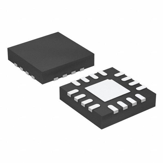
| 供应商器件封装 | 16-WQFN(3x3) |
| 其它名称 | 296-35597-2 |
| 内部驱动器 | 是 |
| 包装 | 带卷 (TR) |
| 商标 | Texas Instruments |
| 安装类型 | 表面贴装 |
| 安装风格 | SMD/SMT |
| 封装 | Reel |
| 封装/外壳 | 16-WFQFN 裸露焊盘 |
| 封装/箱体 | WQFN-16 |
| 工作温度 | -40°C ~ 85°C |
| 工作频率 | 1 MHz |
| 工厂包装数量 | 3000 |
| 恒压 | - |
| 恒流 | - |
| 拓扑 | PWM,升压(升压) |
| 拓扑结构 | Boost |
| 最大工作温度 | + 85 C |
| 最大电源电流 | 3 mA |
| 最小工作温度 | - 40 C |
| 标准包装 | 3,000 |
| 电压-电源 | 2.7 V ~ 6.5 V |
| 电压-输出 | 38V |
| 类型 | Inductive |
| 类型-初级 | 背光 |
| 类型-次级 | 高亮度 LED(HBLED),白色 LED |
| 系列 | TPS61176 |
| 输入电压 | 2.7 V to 6.5 V |
| 输出数 | 6 |
| 输出电流 | 35 mA |
| 输出端数量 | 6 Output |
| 输出类型 | Current Mode |
| 配用 | /product-detail/zh/TPS61176EVM-566/296-37863-ND/4878487 |
| 频率 | 800kHz ~ 1.2MHz |


- 商务部:美国ITC正式对集成电路等产品启动337调查
- 曝三星4nm工艺存在良率问题 高通将骁龙8 Gen1或转产台积电
- 太阳诱电将投资9.5亿元在常州建新厂生产MLCC 预计2023年完工
- 英特尔发布欧洲新工厂建设计划 深化IDM 2.0 战略
- 台积电先进制程称霸业界 有大客户加持明年业绩稳了
- 达到5530亿美元!SIA预计今年全球半导体销售额将创下新高
- 英特尔拟将自动驾驶子公司Mobileye上市 估值或超500亿美元
- 三星加码芯片和SET,合并消费电子和移动部门,撤换高东真等 CEO
- 三星电子宣布重大人事变动 还合并消费电子和移动部门
- 海关总署:前11个月进口集成电路产品价值2.52万亿元 增长14.8%


PDF Datasheet 数据手册内容提取
Product Sample & Technical Tools & Support & Folder Buy Documents Software Community TPS61176 SLVSBM5B–DECEMBER2012–REVISEDAUGUST2015 TPS61176 High-Efficiency 6-Channel WLED Driver Supporting Single-Cell Li-Ion Battery Input 1 Features 3 Description • 2.7-Vto6.5-VV VoltageRange The TPS61176 is an integrated WLED backlight 1 IN driver for tablets or notebook PCs using single-cell • 2.7-Vto24-VBoostInputVoltageRange batteries. It comprises a high-efficiency boost • Integrated2-A/40-VMOSFET converter with an integrated 2-A, 40-V power • 1-MHzSwitchingFrequency MOSFET, and six current sink regulators. The device can drive up to 60 WLEDs. The boost output voltage • AdaptiveBoostOutputtoWLEDVoltages automatically adjusts to the WLED forward voltage to • SixCurrentSinksof35mACapabilityEach improveefficiency. • ±2%(Maximum)CurrentAccuracy The TPS61176 supports mixed dimming mode. The • 1.3%(Typical)CurrentMatching automatic switch between PWM dimming and analog • 100-Hzto22-kHzInputPWMFrequency dimming increases the overall electrical-to-optical efficiency, reducing power of the backlight • MixedDimmingMode:AutomaticSwitchBetween significantly. The switch point can be programmed to AnalogDimmingandPWMDimming 12.5% or 25%. PWM dimming mode can also be – ProgrammableSwitchPoint:25%or12.5% programmed to fixed frequency dimming or direct – ProgrammablePWMDimmingMode:22-kHz PWM dimming. The device supports up to 14-bit PWMDimming,DirectPWMDimming dimming resolution to avoid potential flickering during lowbrightnessdimming. • Upto14-bitDimmingResolution • SupportDownto1%DimmingDutyCycle True shutdown is supported with a driver for an external isolation P-channel MOSFET. When the • InputPWMGlitchFilter device is disabled or the boost output is shorted to • Upto90%Efficiency ground, the isolation PFET is turned off to cut off the • DriverforInputandOutputIsolationPFETfor power path from battery preventing any leakage TrueShutdown current from the battery. The device also integrates soft start, thermal shutdown, WLED open and short • Built-inWLEDOpenandShortProtection protection. Its 16-pin WQFN package provides a • ThermalShutdown space-saving and high-performance WLED driver solution. 2 Applications Backlight for Small and Media Form Factor LCD DeviceInformation(1) DisplaywithSingle-CellorMulti-CellBatteryInput PARTNUMBER PACKAGE BODYSIZE(NOM) TPS61176 WQFN(16) 3.00mm×3.00mm (1) For all available packages, see the orderable addendum at theendofthedatasheet. TypicalApplication L1 2.7V ~ 6.5V 4.7uH D1 Up to 38V VIN C1 2.2uF C2 SW 4.7uF R2 MODE / FAULT PGND R3 1.3M 1M OVP VIN R4 TPS61176 43k VLDO IFB1 IFB2 C3 1uF IFB3 IFB4 PWM PWM / EN IFB5 IFB6 ISET COMP R1 C4 51k GND 0.47uF 1 An IMPORTANT NOTICE at the end of this data sheet addresses availability, warranty, changes, use in safety-critical applications, intellectualpropertymattersandotherimportantdisclaimers.PRODUCTIONDATA.
TPS61176 SLVSBM5B–DECEMBER2012–REVISEDAUGUST2015 www.ti.com Table of Contents 1 Features.................................................................. 1 7.4 DeviceFunctionalModes........................................13 2 Applications........................................................... 1 8 ApplicationandImplementation........................ 17 3 Description............................................................. 1 8.1 ApplicationInformation............................................17 4 RevisionHistory..................................................... 2 8.2 TypicalApplication .................................................17 5 PinConfigurationandFunctions......................... 3 9 PowerSupplyRecommendations...................... 24 6 Specifications......................................................... 4 10 Layout................................................................... 25 6.1 AbsoluteMaximumRatings......................................4 10.1 LayoutGuidelines.................................................25 6.2 ESDRatings ............................................................4 10.2 LayoutExample....................................................25 6.3 RecommendedOperatingConditions.......................4 11 DeviceandDocumentationSupport................. 26 6.4 ThermalInformation..................................................4 11.1 DeviceSupport......................................................26 6.5 ElectricalCharacteristics...........................................5 11.2 CommunityResources..........................................26 6.6 TypicalCharacteristics..............................................7 11.3 Trademarks...........................................................26 7 DetailedDescription.............................................. 9 11.4 ElectrostaticDischargeCaution............................26 7.1 Overview...................................................................9 11.5 Glossary................................................................26 7.2 FunctionalBlockDiagram.......................................10 12 Mechanical,Packaging,andOrderable Information........................................................... 26 7.3 FeatureDescription.................................................10 4 Revision History NOTE:Pagenumbersforpreviousrevisionsmaydifferfrompagenumbersinthecurrentversion. ChangesfromRevisionA(August2013)toRevisionB Page • AddedESDRatingstable,FeatureDescriptionsection,DeviceFunctionalModes,ApplicationandImplementation section,PowerSupplyRecommendationssection,Layoutsection,DeviceandDocumentationSupportsection,and Mechanical,Packaging,andOrderableInformationsection.................................................................................................. 1 ChangesfromOriginal(December2012)toRevisionA Page • Alignedpackagedescriptionthroughoutdatasheet................................................................................................................ 1 2 SubmitDocumentationFeedback Copyright©2012–2015,TexasInstrumentsIncorporated ProductFolderLinks:TPS61176
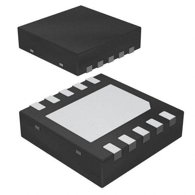
TPS61176 www.ti.com SLVSBM5B–DECEMBER2012–REVISEDAUGUST2015 5 Pin Configuration and Functions RTEPackage 16-PinWQFNwithExposedThermalPad TopView E/LT D DU N OA N W G MF VI S P 16 15 14 13 PWM/ 1 12 OVP EN VLDO 2 11 IFB1 TPS61176 ISET 3 10 IFB2 COMP 4 9 IFB3 5 6 7 8 6 5 4 D B B B N F F F G I I I PinFunctions PIN TYPE DESCRIPTION NAME NUMBER COMP 4 Analog Connectanexternal0.47-µFceramiccapacitortothispinfortheboostloopcompensation. GND 8 Ground Analogground IFB4toIFB6, 5,6,7, Analog Regulatedcurrentsinksinputpins IFB1toIFB3 9,10,11 Full-scaleLEDcurrentsettingpin.Connectaresistortothepintoprogramthefull-scaleLED ISET 3 Analog current. Multi-functionpin.Usethispintoprogramthedimmingmode.Italsofunctionsasadriverfor MODE/FAULT 16 Input externalisolationP-channelMOSFET.(1) OVP 12 Analog Thispinmonitorstheoutputvoltageoftheboostconverterthroughexternalresistordivider. PGND 13 Ground Powerground PWM/EN 1 Input PWMdimmingsignalinputanddeviceenable/disablecontrol.(1) SW 14 Analog DrainoftheinternalpowerMOSFET. VIN 15 Power Supplyinputpin,providespowersupplytothedevice. VLDO 2 Analog Internalpre-regulatoroutput.Connecta1-µFceramiccapacitortothispin. TheGNDpinshouldbeconnectedtotheexposedthermalpadforproperoperation.This ThermalPad — — thermalpadshouldbeconnectedtoanyinternalPCBgroundplanusingmultipleviasforgood thermalperformance. (1) SeeDetailedDescriptionfordetails. Copyright©2012–2015,TexasInstrumentsIncorporated SubmitDocumentationFeedback 3 ProductFolderLinks:TPS61176
TPS61176 SLVSBM5B–DECEMBER2012–REVISEDAUGUST2015 www.ti.com 6 Specifications 6.1 Absolute Maximum Ratings overoperatingfree-airtemperaturerange(unlessotherwisenoted)(1) MIN MAX UNIT VIN,PWM/EN,MODE/FAULT –0.3 7 V SW –0.3 40 V Voltagerange(2) IFB1toIFB6 –0.3 20 V Allotherpins –0.3 3.6 V Continuouspowerdissipation SeeThermalInformation Operatingjunctiontemperature –40 150 °C Storagetemperature,T –65 150 °C stg (1) StressesbeyondthoselistedunderAbsoluteMaximumRatingsmaycausepermanentdamagetothedevice.Thesearestressratings only,whichdonotimplyfunctionaloperationofthedeviceattheseoranyotherconditionsbeyondthoseindicatedunderRecommended OperatingConditions.Exposuretoabsolute-maximum-ratedconditionsforextendedperiodsmayaffectdevicereliability. (2) Allvoltagevaluesarewithrespecttonetworkgroundterminal. 6.2 ESD Ratings VALUE UNIT Human-bodymodel(HBM),perANSI/ESDA/JEDECJS-001(1) ±4000 V Electrostatic Charged-devicemodel(CDM),perJEDECspecificationJESD22-C101(2) ±2000 V (ESD) discharge Machinemodel ±200 (1) JEDECdocumentJEP155statesthat500-VHBMallowssafemanufacturingwithastandardESDcontrolprocess. (2) JEDECdocumentJEP157statesthat250-VCDMallowssafemanufacturingwithastandardESDcontrolprocess. 6.3 Recommended Operating Conditions overoperatingfree-airtemperaturerange(unlessotherwisenoted) MIN NOM MAX UNIT Biasvoltagetodevice(seeFigure18) 2.7 6.5 V V IN Inputvoltagetoinductor(seeFigure18) 2.7 24 V V Outputvoltagerange V 38 V OUT IN L Inductor 4.7 6.8 10 µH C Inputcapacitor 1.0 2.2 µF I C Outputcapacitor 2.2 4.7 10 µF O C COMPcapacitor 0.47 1 µF COMP F InputPWMsignalfrequency 0.1 22 kHz PWM_I T Operatingambienttemperature –40 85 °C A T Operatingjunctiontemperature –40 125 °C J 6.4 Thermal Information TPS61176 THERMALMETRIC(1) RTE(WQFN) UNIT 16PINS R Junction-to-ambientthermalresistance 43 °C/W θJA R Junction-to-case(top)thermalresistance 44.4 °C/W θJC(top) R Junction-to-boardthermalresistance 14.4 °C/W θJB ψ Junction-to-topcharacterizationparameter 0.6 °C/W JT ψ Junction-to-boardcharacterizationparameter 14.3 °C/W JB R Junction-to-case(bottom)thermalresistance 3.3 °C/W θJC(bot) (1) Formoreinformationabouttraditionalandnewthermalmetrics,seetheSemiconductorandICPackageThermalMetricsapplication report,SPRA953. 4 SubmitDocumentationFeedback Copyright©2012–2015,TexasInstrumentsIncorporated ProductFolderLinks:TPS61176
TPS61176 www.ti.com SLVSBM5B–DECEMBER2012–REVISEDAUGUST2015 6.5 Electrical Characteristics V =3.6V,PWM/EN=high,IFBcurrent=20mA,IFBvoltage=450mV,T =–40°Cto+85°C,typicalvaluesareatT = IN A A 25°C(unlessotherwisenoted). PARAMETER TESTCONDITIONS MIN TYP MAX UNIT POWERSUPPLY V Inputvoltagerange 2.7 6.5 V IN V rampdown 2.4 2.5 IN V VINundervoltagelockoutthreshold V IN_UVLO V rampup 2.65 2.7 IN V VINundervoltagelockouthysteresis 250 mV IN_HYS Deviceenable,switching1MHzandno I OperatingquiescentcurrentintoVIN 3 mA q_VIN load PWM/EN=low 1 4 I Shutdowncurrent µA SD PWM/EN=low,T =25°C 1 2 A V VLDOpinoutputvoltage V =3.6V 3 3.3 3.5 V LDO IN PWM/EN V PWM/ENlogichigh 1.2 V H V PWM/ENlogicLow 0.4 V L PWM/ENpininternalpull-down R 400 800 1600 kΩ PD resistor t PWM/ENlogiclowwidthtoshutdown PWM/ENfromhightolow 20 ms SD CURRENTREGULATION V ISETpinvoltage PWM/ENlogichigh 1.02 1.04 1.06 V ISET K Currentmultiplier I =20μA 1024 ISET ISET I =20μA,0°Cto70°C –2% 2% ISET I Currentaccuracy FBx I =20µA,–40°Cto85°C –2.3% 2.3% ISET K (I –I )/(2xI ) I =20μA 0.65% m MAX MIN AVG ISET V =10V,eachpin 1.5 5 IFBx I IFBxpinleakagecurrent µA IFBx_leak V =5V,eachpin 0.5 2 IFBx I Currentsinkmaxoutputcurrent I =35μA,eachpin 35 mA IFBx_max ISET T Currentsinkminimumontime I =20μA,eachpin 0.5 µs FBx_MINON ISET f PWMdimmingfrequency Mode1/Mode3,0°Cto70°C 20 22 27 kHz dim BOOSTOUTPUTREGULATION V IFBxregulationvoltage MeasuredonV ,I =20μA 450 mV IFBx_min IFB(MIN) ISET POWERSWITCH R SwitchMOSFETon-resistance V =3.6V 0.25 0.4 Ω DS(on) IN I SwitchMOSFETleakagecurrent V =40V 2 µA LEAK_SW SW OSCILLATOR f Oscillatorfrequency 0.8 1 1.2 MHz SW D Maximumboostswitchdutycycle 93% max MODE/FAULT TestedasV –V whenmode IN MODE resistorisconnectedbetweenVINpin MODE/FAULTpinvoltageduring V andMODE/FAULTpin;Testedas 0.6 0.9 V MODE modedetectionperiod V whenmoderesistorisconnected MODE betweenMODE/FAULTpinandGND V =0.5V,moderesistoris MODE/FAULTpinpulldowncurrent MODE I connectedbetweenVINpinand 50 80 µA MODE_PD aftermodedetection MODE/FAULTpin Copyright©2012–2015,TexasInstrumentsIncorporated SubmitDocumentationFeedback 5 ProductFolderLinks:TPS61176
TPS61176 SLVSBM5B–DECEMBER2012–REVISEDAUGUST2015 www.ti.com Electrical Characteristics (continued) V =3.6V,PWM/EN=high,IFBcurrent=20mA,IFBvoltage=450mV,T =–40°Cto+85°C,typicalvaluesareatT = IN A A 25°C(unlessotherwisenoted). PARAMETER TESTCONDITIONS MIN TYP MAX UNIT OC,SC,OVPandSS I SwitchMOSFETcurrentlimit 2 2.5 3 A LIM V Outputovervoltageclampthreshold 1.47 1.5 1.53 V OVP_clamp Outputovervoltageshutdown OVPrampup 1.568 1.6 1.632 V V OVP_sd threshold OVPrampdown 1.519 1.55 1.581 OutputshorttoGNDdetection OVPrampup 90 V mV OVP_SC threshold OVPrampdown 50 70 V 1stlevelIFBovervoltagethreshold IFBxcurrentsinkon 7 8.5 10 V OVP_IFB V 2ndlevelIFBovervoltagethreshold IFBxcurrentsinkonoroff 16 18 20 V OVP2_IFB THERMALSHUTDOWN T Thermalshutdownthreshold 160 °C shutdown T Thermalshutdownhysteresis 15 °C hys 6 SubmitDocumentationFeedback Copyright©2012–2015,TexasInstrumentsIncorporated ProductFolderLinks:TPS61176
TPS61176 www.ti.com SLVSBM5B–DECEMBER2012–REVISEDAUGUST2015 6.6 Typical Characteristics Table1.TableOfGraphs TITLE DESCRIPTION FIGURE DimmingEfficiency V =3V,3.6V,4.2V,5V;V =18V,6s6p,20mA/string;PWMFreq=200Hz;Mode Figure1 BAT O 1; L=6.8µH DimmingEfficiency V =3V,3.6V,4.2V,5V;V =21V,7s6p,20mA/string;PWMFreq=200Hz;Mode Figure2 BAT O 1; L=6.8µH DimmingEfficiency V =3V,3.6V,4.2V,5V;V =24V,8s5p,20mA/string;PWMFreq=200Hz;Mode Figure3 BAT O 1; L=6.8µH DimmingEfficiency V =3V,3.6V,4.2V,5V;V =27V,9s4p,20mA/string;PWMFreq=200Hz;Mode Figure4 BAT O 1; L=6.8µH DimmingEfficiency V =5V;V =3V,3.6V,4.2V,5V,7.2V,9V,12V,15V;V =18V,6s6p,20 Figure5 IN BAT O mA/string;PWMFreq=200Hz; Mode1;L=6.8µH(refertoFigure18) DimmingLinearity V =3V,3.6V,4.2V,5V;V =21V,7s6p;R =53kΩ;PWMFreq=200Hz; Figure6 BAT O ISET Mode1 CurrentLimitvsInput V =30V;T =25°C Figure7 O A Voltage SwitchingWaveform V =3.6V;V =18V,6s6p;R =53kΩ;Duty=100%;L=6.8µH Figure11 BAT O ISET SwitchingWaveform V =3.6V;V =18V,6s6p;R =53kΩ;PWMFreq=200Hz;Duty=50%;L=6.8 Figure12 BAT O ISET µH; Mode1 SwitchingWaveform V =3.6V;V =18V,6s6p;R =53kΩ;PWMFreq=200Hz;Duty=10%;L=6.8 Figure13 BAT O ISET µH; Mode1 SwitchingWaveform V =3.6V;V =18V,6s6p;R =53kΩ;PWMFreq=200Hz;Duty=50%;L=6.8 Figure14 BAT O ISET µH; Mode2 SwitchingWaveform V =3.6V;V =18V,6s6p;R =53kΩ;PWMFreq=200Hz;Duty=10%;L=6.8 Figure15 BAT O ISET µH; Mode2 Start-upWaveform V =3.6V;V =18V,6s6p;R =53kΩ;Duty=100%;L=6.8µH Figure16 BAT O ISET Start-upWaveform V =3.6V;V =18V,6s6p;R =53kΩ;PWMFreq=200Hz;Duty=10%;L=6.8 Figure17 BAT O ISET µH; Mode1 100 100 VBAT = 5 V VBAT = 5 V 90 90 Efficiency (%) 7800 VBAT = 3 V VBAT = 3.6 V VBAT = 4.2 V Efficiency (%) 7800 VBAT = 3 V VBAT = 3.V6 V = 21 VVB, A7Ts =6 p4,. 2 V O 20 mA/string V = 18 V, 6s6p, 60 60 O 20 mA/string 50 50 0 20 40 60 80 100 0 20 40 60 80 100 Dimming Duty Cycle (%) C002 Dimming Duty Cycle (%) C001 Figure1.EfficiencyvsDimmingDutyCycle Figure2.EfficiencyvsDimmingDutyCycle Copyright©2012–2015,TexasInstrumentsIncorporated SubmitDocumentationFeedback 7 ProductFolderLinks:TPS61176
TPS61176 SLVSBM5B–DECEMBER2012–REVISEDAUGUST2015 www.ti.com 100 100 V = 5 V BAT V = 5 V BAT 90 90 %) %) 80 80 Efficiency ( 70 VBAT = 3 V VBAT = 3.6 V VBAT = 4.2 V Efficiency ( 70 VBAT = 3 VV BAT = 3.6 V VBAT = 4.2 V V = 24 V, 8s5p, V = 27 V, 9s4p, O O 60 20 mA/string 60 20 mA/string 50 50 0 20 40 60 80 100 0 20 40 60 80 100 Dimming Duty Cycle (%) C003 Dimming Duty Cycle (%) C004 Figure3.EfficiencyvsDimmingDutyCycle Figure4.EfficiencyvsDimmingDutyCycle 100 140 V = 15 V BAT 95 120 A) VBAT = 5 V m 100 %) 90 nt ( Efficiency ( 8805 VBAT V=B A4T. 2= V 5 V VBAT = 7V.2BA VT = 9 V Output Curre 6800 VBAT = 4.2 V 75 VBAT =V 3B AVT = 3.6 V V20O m= A18/s tVri,n 6gs, 6VpIN, = 5 V VBAT = 12 V I- O 2400 VBAT = 3 VV BAT = 3.6 V 70 0 0 20 40 60 80 100 0 20 40 60 80 100 Dimming Duty Cycle (%) C005 Dimming Duty Cycle (%) C006 Figure5.EfficiencyvsDimmingDutyCycle Figure6.DimmingLinearity 2.7 V = 30 V A) 2.5 O mit ( Li2.3 nt e urr2.1 C h c wit1.9 S - M ILI1.7 1.5 2.7 3.0 3.3 3.6 3.9 4.2 4.5 4.8 VI - Input Voltage (V) C007 Figure7.SwitchCurrentLimitvsInputVoltage 8 SubmitDocumentationFeedback Copyright©2012–2015,TexasInstrumentsIncorporated ProductFolderLinks:TPS61176
TPS61176 www.ti.com SLVSBM5B–DECEMBER2012–REVISEDAUGUST2015 7 Detailed Description 7.1 Overview The TPS61176 is a high-efficiency, multi-channel WLED driver for tablet and notebook backlighting applications. Because a greater number of WLED diodes are required to provide high brightness backlighting for high resolution panels, the WLED diodes must be arranged in parallel strings. Having more WLED diodes in a string reduces the number of parallel strings and thus improves overall current matching; however, the efficiency of the boost regulator drops due to the high output voltage. Therefore, six current sink regulators of high current matchingcapabilityareintegratedintheTPS61176toprovidetheWLEDconnectionflexibilityandtoimprovethe overall power efficiency. The six channels can also be combined as 2 or 3 channels to drive high brightness WLEDdiodes. The TPS61176 has integrated all of the key function blocks to power and control up to 60 WLED diodes. The device consists of a boost converter with 2-A, 40-V power MOSFET, six 35-mA current sink regulators and protectioncircuitforovercurrent,overvoltage,openLED,shortLEDandoutputshortcircuitfailures. ThedeviceacceptsPWMdimmingsignalandimplementsmixeddimmingmode.Whenthedimmingdutycycleis high, analog dimming mode works, under which the device controls the DC current of the WLED diodes to realize brightness dimming; when the dimming duty cycle is low, the device switches to PWM dimming mode automatically, so the current of WLED diodes is turned on and off in a high frequency to realize dimming. The automatic switch between analog and PWM dimming modes can leverage the advantages of the two modes: increasing the electrical-to-optical efficiency by analog dimming and avoiding potential color shift issue. The switchpointcanbeprogrammedtoeither25%or12.5%bytheexternalresistorconnectedatMODE/FAULTpin. Copyright©2012–2015,TexasInstrumentsIncorporated SubmitDocumentationFeedback 9 ProductFolderLinks:TPS61176
TPS61176 SLVSBM5B–DECEMBER2012–REVISEDAUGUST2015 www.ti.com 7.2 Functional Block Diagram Optional L Diode VIN VOUT C1 R2 C5 C6 2.2uF 82k 100pF 2.2uF C3 4.7uF MODE/FAULT SW R3 1M Dimming Mode Detection OVP OVP VIN Fault protection OVC R4 Short to GND 43k VLDO UVLO / R Q Protection Internal C2 Regulator S OCP 1uF OSC Slope S VOVP PGND Compensation Detector Comp regulation IFB1 Error IFB2 COMP Amp VOVP IFB no use IFB3 Open /Short IFB4 LED IFB5 C4 OVP IFB6 0.47uF Shut Down IFB1 EN Disable Dimming Mode Dimming EA Detection Selection Control RSET Analog Current LED Dimming Mirror Current Current Sink GND R1 51k Current Sink IFB2 PWM Duty PWM/EN decoding Control Current Sink IFB3 circuit Circuit PWM Current Sink IFB4 dimming PWM Signal Current Sink IFB5 OSC Generator Current Sink IFB6 7.3 Feature Description 7.3.1 SupplyVoltage The TPS61176 can support single-cell Li-ion battery input directly. It has a built-in linear regulator to generate supply for internal analog and logic circuits. The VLDO pin, output of the regulator, should be connected to a 1- µF bypass capacitor for the regulator to be controlled in a stable loop. VLDO pin does not have current sourcing capabilityforexternaluse. If the device is used in a multi-cell battery system, the battery cannot be connected to VIN pin directly. In this case, connect a 3.3-V or 5-V power rail to bias the VIN pin and connect the battery voltage to the inductor. The VIN pin only consumes less than 3 mA for normal operation. Refer to Application and Implementation for more details. 10 SubmitDocumentationFeedback Copyright©2012–2015,TexasInstrumentsIncorporated ProductFolderLinks:TPS61176
TPS61176 www.ti.com SLVSBM5B–DECEMBER2012–REVISEDAUGUST2015 Feature Description (continued) 7.3.2 BoostConverter The boost converter of the TPS61176 has a fixed switching frequency of 1 MHz and uses current-mode control. A 2-A, 40-V power MOSFET is integrated so the device has a strong output driving capability. A 0.47-µF to 1-µF capacitor should be connected at COMP pin to ensure stable output over the full input and output voltage ranges assuming the recommended inductance and output capacitance values shown in Recommended Operating Conditions are used. The COMP pin is very sensitive, so careful layout is required to make sure no noise is coupledtoit. The output voltage of the boost is automatically set by the device to minimize the voltage drop across the IFBx (IFB1 ~ IFB6) pins. Normally the voltage across each WLED string is not same, so the voltages at IFBx pins are different. The device regulates the lowest IFBx voltage to 450 mV, and consistently adjusts the boost output voltage to account for any change of WLED forward voltage drop. If the input voltage is higher than the strings' forward voltage drop (for example, at low duty cycles), the boost converter can’t regulate the output due to its minimum duty-cycle limitation. In this case, increasing the number of WLED diodes in series is helpful to provide enoughheadroomfortheconvertertoboostthevoltage. 7.3.3 CurrentSinks The six current sink regulators embedded in TPS61176 can output up to 35 mA current each. By regulating the current sinks, the TPS61176 controls the current of the WLED strings to realize brightness dimming. The full- scalecurrentperchannelisprogrammedbytheresistoratISETpinaccordingtoEquation1. V IFBx_full = ISET_full ´KISET R ISET where • I ,full-scalecurrentperchannel FBx_full • K =1024(Currentmultiple) ISET • V =1.04V(ISETpinvoltageunder100%dimmingdutycycle) ISET_full • R =ISETpinresistor (1) ISET 7.3.4 IFBxPinUnused If fewer than six channels are used, a user can easily disable the unused channel(s) by shorting the corresponding IFBx pin(s) to ground. The TPS61176 detects IFBx pins short status during the start-up process anddisablestheunusedchannel(s)beforetheboostconverterstartsswitching. 7.3.5 EnableandStart-up The TPS61176 receives a PWM signal at PWM/EN pin to implement the dimming as well as to enable and disable the device. When a PWM signal (high logic or PWM pulse) is input, the device is enabled automatically; when the PWM signal is pulled low for more than 20 ms, the device is disabled and enters into shutdown mode. In shutdown mode, the boost converter stops switching, and the MODE/FAULT pin is internally pulled to VIN to turn off external isolation MOSFET for true shutdown. The input supply current at VIN pin is 4 µA (maximum) in shutdown mode. In order to avoid fault-triggered shutdown during dimming, the PWM dimming signal should haveahigherfrequencythan100Hz. Once enabled by PWM input, the TPS61176 enters the start-up process. The internal regulator is enabled first to supply current to internal circuits. Then the device detects the R at MODE/FAULT pin to set the dimming MODE mode. The TPS61176 can detect if the mode resistor is connected between VIN pin and MODE/FAULT pin or connected between MODE/FAULT pin and GND pin. If the mode resistor is detected to be between VIN pin and MODE/FAULT pin, which indicates an external isolation P-channel MOSFET is connected, the MODE/FAULT pin will be pulled down by an internal current sink to turn on the isolation MOSFET after the detection process. The device also checks the status of all IFBx pins (short-to-ground or not) to disable any unused channels. There is no special time sequence requirement of VIN and PWM signals for start-up. If PWM signal is input first, the devicestartsupwhenVINpowersup. Copyright©2012–2015,TexasInstrumentsIncorporated SubmitDocumentationFeedback 11 ProductFolderLinks:TPS61176
TPS61176 SLVSBM5B–DECEMBER2012–REVISEDAUGUST2015 www.ti.com Feature Description (continued) The dimming mode and IFBx status detection process lasts about 4 ms, during which the MODE/FAULT pin outputs a high voltage (V – 0.6 V, typical) to keep the isolation MOSFET off. When the 4-ms detection window IN ends, an internal current sink pulls the MODE/FAULT pin low to turn on the isolation MOSFET. Another 4-ms time window then starts and, at the end of the window, the device detects the OVP pin voltage. If the OVP voltage V is still lower than V ramp-up threshold (90 mV typical), which normally indicates output short- OVP OVP_SC to-groundissuehappens,theboostremainsoff,andtheMODE/FAULTpinispulleduptoVINimmediatelybyan internal resistor to turn off the isolation MOSFET. In this case, the device restarts only after a power-on reset (POR)togglingorPWMtoggling.PORtogglingmeanstheVINpinvoltageispulledbelowUVLOfallingthreshold first and then pulled above UVLO rising threshold to restart the device; PWM toggling means pulling PWM/EN low for more than 20 ms to disable the device and then apply PWM signal (high logic or PWM pulse) to restart the device. If OVP voltage V is higher than V ramp up threshold, indicating no short to ground issue is OVP OVP_SC detected,booststartsswitchingtoraisetheoutputvoltage.Softstartisimplementedbygraduallyrampingupthe reference voltage of the error amplifier to prevent voltage overshoot and in-rush current. The capacitor at COMP pin can adjust the soft-start speed. Larger capacitance leads to slower start-up. A 0.47-µF to 1-µF COMP capacitorisrecommended. 7.3.6 BrightnessDimmingControl The TPS61176 receives the PWM dimming signal at PWM/EN pin. An internal PWM decoding circuit detects the on time and the period of the PWM signal and calculates the duty cycle information. The device controls the current-sink-regulatoroutputcurrentaccordingtothedutycycletorealizethebrightnessdimming. The device supports mixed dimming mode, which leverages the advantages of both analog dimming and PWM dimming modes. When the dimming duty cycle is high, analog-dimming mode is auto-implemented, increasing the electrical-to-optical efficiency and reducing the power budget for the backlight; when the dimming duty cycle is low, PWM dimming mode is auto-implemented, eliminating potential color shift effect which normally happens when the DC current of WLED diode goes low. The switch point between the analog dimming mode and PWM dimmingmodecanbeprogrammedbythemoderesistorconnectedatMODE/FAULTpin. The TPS61176 provides four dimming mode options as shown in Table 2. Besides two different switch point options: 25% or 12.5%, the device also offers two different PWM dimming mode options: direct PWM dimming or 22-kHzfixed-frequencyPWMdimming.RefertoDimmingModesforthedetailsofdifferentdimmingmodes. Different mode resistor values set the different dimming modes. 5% or higher precision resistor should be used for the mode resistor. When an isolation P-channel MOSFET is connected, the mode resistor must be connected between VIN pin and MODE/FAULT pin; when the isolation MOSFET is not connected, the mode resistor should be connected between MODE/FAULT pin and ground. If there is no resistor connected at MODE/FAULT pin, which is only allowed when the isolation MOSFET is not connected, default mode (Mode 1) will be selected. RefertoApplicationandImplementationsectionformoredetails. Table2.DimmingModeSetting MODE SWITCHPOINTBETWEEN MODE DIMMINGMODE RESISTOR ANALOGANDPWMDIMMING Mode1 Analogdimming+22-kHzfixed-frequencyPWM 1.3MΩ(5%) 25% (Defaultmode) dimming Mode2 620kΩ(5%) Analogdimming+directPWMdimming 25% Mode3 220kΩ(5%) Analogdimming+22-kHzfixed-frequencyPWM 12.5% dimming Mode4 82kΩ(5%) Analogdimming+directPWMdimming 12.5% 12 SubmitDocumentationFeedback Copyright©2012–2015,TexasInstrumentsIncorporated ProductFolderLinks:TPS61176
TPS61176 www.ti.com SLVSBM5B–DECEMBER2012–REVISEDAUGUST2015 7.4 Device Functional Modes 7.4.1 DimmingModes 7.4.1.1 AnalogDimmingMode In analog dimming mode, the brightness dimming is realized by controlling the DC current of WLED diodes. Because the forward voltage of a WLED diode drops when its DC current reduces, the required output voltage can become lower when dimming duty cycle goes low, reducing the power budget for the backlight and allowing moresystempowersaving. Inanalogdimmingmode,thecurrentofIFBxisregulatedaccordingtoEquation2: V V I = ISET ´K = ISET_full ´K ´Duty FBx ISET ISET R R ISET ISET where • I ,currentperstring FBx • V ,(ISETpinvoltageduringanalogdimming) ISET • K =1024(Currentmultiple) ISET • V =1.04V(ISETpinvoltagewith100%dimmingdutycycle) ISET_full • R =ISETpinresistor ISET • Duty=dutycycleofthePWMsignal (2) 7.4.1.2 PWMDimming When the dimming duty cycle is below the switch point, PWM dimming mode is automatically implemented. In this mode, the current sink regulators are turned on and off according to the PWM duty cycle information, so the illumination of WLEDs is intermittent. At frequencies higher than a human eye critical flicker frequency, the brightness is the same as the average brightness of the fluctuating light, thus controlling the duty cycle can realizethebrightnessdimming. While a current sink regulator is turned on during PWM dimming, its output current is equal to the DC current at the switch point. For example, if the switch point is set to 25%, the regulator's output current during the ON phase is equal to I × 25%, and the ON phase's duty cycle Duty' is equal to Duty / 25%, where Duty is the FBx_full input PWM signal's duty cycle information. Then the average current during PWM dimming can be still equal to I × Duty. This design is in order to keep the brightness consistency between analog dimming and PWM FBx_full dimming and avoid any abrupt brightness change around the switch point. If the switch point is set to 12.5%, the regulator's output current during the ON phase is equal to I × 12.5%, and the ON phase duty cycle Duty is FBx_full equaltoDuty/12.5%(seeFigure8). Copyright©2012–2015,TexasInstrumentsIncorporated SubmitDocumentationFeedback 13 ProductFolderLinks:TPS61176
TPS61176 SLVSBM5B–DECEMBER2012–REVISEDAUGUST2015 www.ti.com Device Functional Modes (continued) Analog Dimming PWM Dimming D=100% D=80% D=60% D=25% D=12.5% D=6.25% PWM Input TON TPER IFBx_Full 80% 60% IFBx 50% D’=50% D’=25% 25% 0A (a).Mixed Dimming Mode with switch point=25% Analog PWM Dimming Dimming D=100% D=80% D=60% D=25% D=12.5% D=6.25% PWM Input TON TPER IFBx_Full 80% 60% IFBx 50% 25% D’=50% 12.5% 0A (b).Mixed Dimming Mode with switch point=12.5% Figure8. MixedDimmingMode Generally,theaveragecurrentofanLEDstringinPWMdimmingmodeisequalto V I = ISET_full ´K ´Duty FBx_PWM ISET R ISET where • I ,averagecurrentperstringinPWMdimmingmode FBx_PWM • V =1.04V(ISETpinvoltagewith100%dimmingdutycycle) ISET_full • K =1024(Currentmultiple) ISET • R =ISETpinresistor ISET • Duty=dutycycleofthePWMsignal (3) 14 SubmitDocumentationFeedback Copyright©2012–2015,TexasInstrumentsIncorporated ProductFolderLinks:TPS61176
TPS61176 www.ti.com SLVSBM5B–DECEMBER2012–REVISEDAUGUST2015 Device Functional Modes (continued) The frequency of the current sink regulators ON and OFF control depends on which PWM dimming mode is set. The TPS61176 provides two different PWM dimming modes: direct PWM dimming mode and 22-kHz fixed frequencyPWMdimmingmode. In direct PWM dimming mode, the current sinks are turned ON and OFF with the same frequency detected from the input PWM signal. The advantage of this mode is the dimming frequency can be adjusted freely. In addition, it is easy to achieve high dimming resolution in direct PWM dimming mode: with lower input PWM frequency, the higher dimming resolution can be detected and output. For example, when the input PWM frequency is 100 Hz, 14-bit resolution can be achieved; when the input PWM frequency is 20 kHz, 9-bit resolution is achieved. So if highresolutionisrequired,100-Hzor200-Hzdimmingfrequencyisrecommended.TheTPS61176isdesignedto minimize the AC ripple on the output capacitor during PWM dimming. Careful passive component selection is also crucial to minimize AC ripple on the output capacitor. In order to further avoid the potential audible noise, input PWM frequency out of audible frequency range is recommended. See Application and Implementation for moreinformation. In 22-kHz fixed frequency PWM dimming mode, current sinks are turned on and off according to the duty cycle information detected from the input PWM signal but with an internally fixed frequency. This mode facilitates the application where the input PWM signal frequency cannot be adjusted outside the audio frequency range. Thus inthismodetheaudiblenoiseiseliminatedcompletely. The human eye is much more sensitive to the brightness change at low brightness compared to at high brightness, so in order to improve the visual experience and avoid any potential flickering perception, high- resolution dimming is implemented in PWM dimming mode. The TPS61176 can achieve up to 14-bit dimming resolution during the PWM dimming. Generally, higher resolution can be achieved with lower input PWM frequency.RefertoTable3fordetaileddimmingresolutioninformation. Table3.DimmingResolutionInformationinPWMDimmingMode DIMMINGMODE INPUTPWMFREQUENCY DIMMINGRESOLUTIONINPWMDIMMINGMODE 100Hz~4.5kHz 12-bit 4.5kHz~9Hz 11-bit Mode1 9kHz~18kHz 10-bit 18kHz~20kHz 9-bit 100Hz~1kHz 14-bit 1kHz~2kHz 13-bit 2kHz~4kHz 12-bit Mode2 4kHz~8kHz 11-bit 8kHz~16kHz 10-bit 16kHz~20kHz 9-bit 100Hz~5kHz 12-bit Mode3 5kHz~10kHz 11-bit 10kHz~20kHz 10-bit 100Hz~1.2kHz 14-bit 1.2kHz~2.4kHz 13-bit Mode4 2.4kHz~4.8kHz 12-bit 4.8kHz~9.6kHz 11-bit 9.6kHz~20kHz 10-bit 7.4.2 OvervoltageProtection The output voltage of the boost converter is detected by the OVP pin. The overvoltage-protection threshold can be programmed by an external resistor divider (R3 and R4 in the Typical Application), allowing the usage of low voltage-rating Schottky diode in a low output-voltage application. The correct divider ratio is important for optimum operation of the device. Use the following guidelines to choose the divider value. It can be noise sensitive if R and R have high impedance. Careful layout is required. Also, choose lower resistance upper down valuesforR andR whenpowerdissipationallows. upper down Copyright©2012–2015,TexasInstrumentsIncorporated SubmitDocumentationFeedback 15 ProductFolderLinks:TPS61176
TPS61176 SLVSBM5B–DECEMBER2012–REVISEDAUGUST2015 www.ti.com Step1. Determinethemaximumoutputvoltage,V ,forthesystemaccordingtothenumberofseries OUT WLEDs. Step2. SelectR resistorvalue(1MΩforatypicalapplication;alowervaluesuchas100kΩ foranoisy upper environment). Step3. CalculateR byusingEquation4. down æR ö V =ç upper +1÷´V OUT ç ÷ OVP_clamp èRdown ø where • V =1.5V (4) OVP_clamp When the overvoltage threshold V is reached, the TPS61176 detects if there are any LED strings open, OVP_clamp first by sensing whether there is current on IFBx pin. If any string is open, the corresponding current sink is disabled and removed from regulation. Subsequently, the output voltage drops down and is regulated to a voltage for the connected WLED strings. The IFBx current of the connected WLED strings keeps in regulation duringthewholetransition.Ifanopenstringisreconnectedagain,aPORtogglingorPWMtogglingisrequiredto reactivateapreviouslydeactivatedstring.TheTPS61176shutsdownandkeepsoffwhenitdetectsthatallofthe WLED strings are open. In this case, a POR toggling or PWM toggling is required to restart the device. If there isn’tanystringopen,theTPS61176regulatestheboostoutputattheover-voltagethreshold. If the output voltage cannot be regulated at the value set by Equation 4 and keeps rising, once the OVP pin voltage exceeds V rising threshold (1.6 V typical), the boost stops switching. When the OVP voltage falls OVP_sd belowV fallingthreshold(1.55Vtypical),theboostrecoverstoswitch.Duringtheprocess,theIFBxcurrent OVP_sd oftheconnectedWLEDstringskeepsinregulation. 7.4.3 CurrentSinkOpenProtection If any IFBx pin voltage exceeds the 1st level IFB overvoltage threshold (8.5 V typical) when its current sink is turned on, the TPS61176 turns off this current sink and removes it from output regulation loop. The current regulation of the remaining IFBx pins is not affected. This situation often occurs when there are several shorted WLED diodes in one string. WLED mismatch typically does not create such large voltage difference among WLED strings. The TPS61176 shuts down when it detects that all of the IFBx pin voltages exceed the threshold. Inthiscase,aPORtogglingorPWMtogglingisrequiredtorestartthedevice. If any IFBx pin voltage exceeds the 2nd level IFB overvoltage threshold (18 V typical), no matter whether the current sink is turned on or off, the TPS61176 shuts down immediately to avoid potential over stress damage at IFBxpin.APORtogglingorPWMtogglingisrequiredtorestartthedevice. 7.4.4 OvercurrentandShortCircuitProtection The TPS61176 has a pulse-by-pulse overcurrent limit of 2 A (minimum). The boost power MOSFET is turned off when the inductor current reaches this current limit threshold, and it remains off until the beginning of the next switchingcycle.Thisprotectsthedeviceandexternalcomponentunderoverloadconditions. Under severe overload or short-circuit conditions, if the OVP pin voltage is detected below V ramp-down OVP_SC threshold (70 mV typical), The TPS61176 shuts down, and the MODE/FAULT pin is pulled to VIN by an internal switch immediately. As a result, the external isolation MOSFET can be turned off at once, cutting off the power pathfrominputtooutput.ThedevicerestartsafteraPORtogglingorPWMtoggling. 7.4.5 ThermalProtection An internal thermal shutdown turns off the device when the typical junction temperature of 160°C is exceeded. Thedeviceisreleasedfromshutdownautomaticallywhenthejunctiontemperaturedecreasesby15°C. 16 SubmitDocumentationFeedback Copyright©2012–2015,TexasInstrumentsIncorporated ProductFolderLinks:TPS61176
TPS61176 www.ti.com SLVSBM5B–DECEMBER2012–REVISEDAUGUST2015 8 Application and Implementation NOTE Information in the following applications sections is not part of the TI component specification, and TI does not warrant its accuracy or completeness. TI’s customers are responsible for determining suitability of components for their purposes. Customers should validateandtesttheirdesignimplementationtoconfirmsystemfunctionality. 8.1 Application Information The TPS61176 provides a high-performance LED lighting solution for tablets, notebooks and other low power LCD backlit displays. The device can drive 6 strings of 10 series LEDs in a compact and high efficient solution. The boost voltage can be set with a resistor divider on the OVP pin. The LED current is controlled via a logic level PWM input and the LED current level is set using an I resistor. Boost compensation can be adjusted SET usingacapacitorontheCOMPpin. 8.2 Typical Application 8.2.1 Single-CellBatteryInputApplication TPS61176's VIN pin voltage range is from 2.7 V to 6.5 V, so it can support single-cell battery input directly. If isolation MOSFET is connected, the mode resistor must be connected between VIN pin and MODE/FAULT pin as shown in Figure 9; if isolation MOSFET is not connected, the mode resistor can be connected between VIN pin and GND as shown in Figure 10. If there is no resistor connected at MODE/FAULT pin, which is only allowed whentheisolationMOSFETisnotconnected,defaultmode(Mode1)willbeselected. L1 2.7V~6.5V Q1 4.7uH D1 Up to 38V VIN C6 C1 R2 C5 D2 2.2uF 2.2uF 1.3M 100pF C2 SW 4.7uF MODE/FAULT R3 PGND 1M OVP VIN R4 TPS61176 43k VLDO IFB1 IFB2 C3 1uF IFB3 IFB4 IFB5 PWM PWM /EN IFB6 ISET COMP R1 C4 51k GND 0.47uF Figure9. TypicalApplications(Single-CellBatteryInputApplication) Copyright©2012–2015,TexasInstrumentsIncorporated SubmitDocumentationFeedback 17 ProductFolderLinks:TPS61176
TPS61176 SLVSBM5B–DECEMBER2012–REVISEDAUGUST2015 www.ti.com Typical Application (continued) L1 2.7V~ 6.5V 4.7uH D1 Up to 38V VIN C1 2.2uF C2 SW 4.7uF R2 MODE /FAULT PGND R3 1.3M 1M OVP VIN R4 TPS61176 43k VLDO IFB1 IFB2 C3 1uF IFB3 IFB4 IFB5 PWM PWM /EN IFB6 ISET COMP R1 C4 51k GND 0.47uF Figure10. TypicalApplication(Single-CellBatteryInputWithoutIsolationMOSFETApplication) 8.2.1.1 DesignRequirements ForTPS61176typicalapplications,usetheparameterslistedinTable4asinputparameters. Table4.DesignParameters DESIGNPARAMETER EXAMPLEVALUE Minimuminputvoltage 2.7V Outputvoltage Upto38V NumberofseriesLED upto8 Switchingfrequency 1MHz,typical LEDcurrent Upto35mA 8.2.1.2 DetailedDesignProcedure 8.2.1.2.1 InductorSelection Because the selection of the inductor affects the power supply steady-state operation, transient behavior, loop stability, and the boost converter efficiency, the inductor is the most important component in switching power regulator design. There are three specifications most important to the performance of the inductor: inductance value, DC resistance and saturation current. TPS61176 is designed to work with inductor values between 4.7 µH and 10 µH. A 4.7-µH inductor is typically available in a smaller or lower profile package, while a 10-µH inductor produces lower inductor ripple. If the boost output current is limited by the overcurrent protection of the device, usinga10-µHinductorcanmaximizethecontrolleroutputcurrentcapability. Inaboostregulator,theinductorDCcurrentcanbecalculatedasEquation5. Vout´Iout I = DC Vin´h where • Vout=boostoutputvoltage • Iout=boostoutputcurrent • Vin=boostinputvoltage 18 SubmitDocumentationFeedback Copyright©2012–2015,TexasInstrumentsIncorporated ProductFolderLinks:TPS61176
TPS61176 www.ti.com SLVSBM5B–DECEMBER2012–REVISEDAUGUST2015 • η=powerconversionefficiency,use85%forTPS61176normalapplications (5) Theinductorcurrentpeak-to-peakripplecanbecalculatedasEquation6. 1 I = PP æ 1 1 ö L´çèVout-Vin+ Vin÷ø´FS where • I =inductorpeak-to-peakripple PP • L=inductorvalue • F =Switchingfrequency S • Vout=boostoutputvoltage • Vin=boostinputvoltage (6) Therefore,thepeakcurrentseenbytheinductoriscalculatedwithEquation7. I I =I + PP P DC 2 (7) Select the inductor with saturation current over the calculated peak current. To calculate the worse case inductor peakcurrent,useminimuminputvoltage,maximumoutputvoltageandmaximumloadcurrent. Converter efficiency is dependent on the resistance of its high current path and switching losses associated with the internal switch and external power diode. Although the TPS61176 has optimized the internal switch resistance, the overall efficiency is affected by the inductor’s DC resistance (DCR). Lower DCR improves efficiency. However, there is a trade-off between DCR and inductor footprint. Furthermore, shielded inductors typicallyhavehigherDCRthanunshieldedones. Note that inductor values can have ±20% tolerance with no current bias. When the inductor current approaches saturation level, its inductance can decrease 20% to 35% from the 0-A value depending on how the inductor vendordefinessaturation.Table5liststherecommendedinductors. Table5.RecommendedInductorsfortheTPS61176 PARTNUMBER L(µH) DCR(mΩ) I (A) SIZE(LxWxHmm) VENDOR SAT PCMB051H-4R7MS 4.7 78 4.0 5.4x5.2x1.8 Cyntec PCMB051H-6R8MS 6.8 107 3.4 5.4x5.2x1.8 Cyntec PCMB051H-100MS 10 140 3 5.4x5.2x1.8 Cyntec LPS4018-472ML 4.7 125 1.9 4.0x4.0x1.8 Coilcraft LPS4018-103ML 10 200 1.3 4.0x4.0x1.8 Coilcraft A915AY–4R7M 4.7 38 1.87 5.2x5.2x3 TOKO A915AY–100M 10 75 1.24 5.2x5.2x3 TOKO 8.2.1.2.2 OutputCapacitorSelection The output capacitor is mainly selected to meet the requirement for the loop stability and the output ripple. The loop is designed to be stable with an output capacitor within 2.2-µF to 10-µF range. This output ripple is related to the capacitor’s capacitance and its equivalent series resistance (ESR). Due to its low ESR, the ripple caused by ESR could be neglected for ceramic capacitors. Assuming a capacitor with zero ESR, the minimum capacitanceneededforagivenripplecanbecalculatedwithEquation8. (Vout-Vin)´Iout Cout = Vout´F ´Vripple S where • Vripple=peak-to-peakoutputripple. (8) Copyright©2012–2015,TexasInstrumentsIncorporated SubmitDocumentationFeedback 19 ProductFolderLinks:TPS61176
TPS61176 SLVSBM5B–DECEMBER2012–REVISEDAUGUST2015 www.ti.com Note that capacitor degradation increases the ripple much. Select the capacitor which has less degradation at the output voltage. If the output ripple is too large, change a bigger capacitor could be helpful. Normally, X5R ±10%orbettercapacitorsarerecommended. 8.2.1.2.3 SchottkyDiodeSelection The TPS61176 demands a low forward voltage, high-speed rectification and low capacitance schottky diode for optimum efficiency. Ensure that the diode average and peak current rating exceeds the average output current and peak inductor current. In addition, the diode’s reverse breakdown voltage must exceed the open LED protectionvoltage.VishaySS2P5,MSS1P4,andNXPPMEG4010EPKarerecommendedfortheTPS61176. 8.2.1.2.4 IsolationFETSelection The TPS61176 provides a gate driver at MODE/FAULT pin to drive an external P-channel MOSFET which can act as an isolation MOSFET. When the device is disabled or output short to ground issue happens, MODE/FAULTpincanturnofftheisolationMOSFETtocutoffthepowerpathfromthebatterytotheoutput.The source of the MOSFET should be connected to the battery input, and an external resistor must be connected between the source and gate of the MOSFET to keep the FET off when the device is disabled. This gate resistor also acts as a mode resistor to select the dimming mode. To turn on the isolation MOSFET, an internal current sink pulls MODE/FAULT pin low. When output short to ground fault happens, an internal switch pulls up the MODE/FAULTpintoVIN,turningofftheisolationMOSFETimmediately. When the isolation FET is turned on during start-up, an inrush current will flow through the MOSFET from battery to charge the output capacitor. If the peak current is too large, a capacitor can be connected between the source and the gate of the isolation MOSFET to control the turning on speed (C5 in Figure 9), thus controlling the inrush current.Normally,a100-pFto1-nFcapacitorisrecommended. During output short to ground protection process, the catch diode (D2 in Figure 9) may be forward biased to provide the continuous current of the inductor when the isolation FET is turned off. In this case, the drain of the isolation FET swings below ground. The voltage across the isolation FET can be momentarily greater than the input voltage. Therefore, select at least 10-V maximum input MOSFET. Adding a capacitor parallel with D2 (refer toFigure9)couldalsohelpreducethevoltageacrossMOSFETwhenthisfailurehappens.TheONresistanceof the MOSFET has large impact on power conversion efficiency because the MOSFET carries the input current. Select a MOSFET with R less than 100 mΩ to limit the power losses. In order to detect larger than 1 M ds(on) R correctly,thegateleakageofisolationMOSFETshouldbelessthan0.1 µA. Mode In multi-cell battery input applications, if the isolation MOSFET is connected, the voltage at MODE/FAULT pin may exceed its maximum rating voltage 7 V when the device is disabled or output short to ground issue happens.Inordertopreventthisoverstressdamange,isolationMOSFETcan'tbeconnected. 8.2.1.2.5 AudibleNoiseReduction Output voltage of the controller also ripples due to the load transient that occurs during PWM dimming. If the PWM dimming frequency is in the audible frequency range, the ripple can produce audible noises on the output ceramic capacitor. There are two ways of reducing or eliminating the audible noise. The first way is to reduce the amount of the output ripple, and therefore minimize the audible noise. The TPS61176 adopts a patented technology to limit this type of output ripple even with the minimum recommended output capacitance. The second way is to select PWM dimming frequency outside the audible frequency range to eliminate the audible noise completely. However, in some applications, the input PWM signal frequency range couldn’t be adjusted outsidetheaudiblefrequencyrange.Tosolvethisproblem,thedeviceprovidesthe22-kHzfixedfrequencyPWM dimming mode. In this dimming mode, no matter what the input PWM frequency is, the PWM dimming is implemented at 22 kHz, which is outside the audible frequency range, saving the effort to adjust the input PWM frequency. 20 SubmitDocumentationFeedback Copyright©2012–2015,TexasInstrumentsIncorporated ProductFolderLinks:TPS61176
TPS61176 www.ti.com SLVSBM5B–DECEMBER2012–REVISEDAUGUST2015 8.2.1.3 ApplicationCurves Output Output Voltage Voltage 100mV/div 100mV/div AC AC SW SW Voltage Voltage 10V/div 10V/div DC DC Inductor Inductor Current Current 1A/div 1A/div DC DC Output Output Current Current 100mA/div DC DUTY=100% 100mA/div PWMFREQ=200HZ;DUTY=50%;MODE1 DC t-Time-1µs/div t-Time-1µs/div Figure11.SwitchingWaveform Figure12.SwitchingWaveform Output PWMFREQ=200HZ;DUTY=10%;MODE1 Output Voltage Voltage 100mV/div 100mV/div AC AC SW SW Voltage Voltage 10V/div 10V/div DC DC Inductor Inductor Current Current 1A/div 1A/div DC DC Output Output Current Current 100mA/div 100mA/div DC DC PWMFREQ=200HZ;DUTY=50%;MODE2 t-Time–20µs/div t-Time-1µs/div Figure13.SwitchingWaveform Figure14.SwitchingWaveform Output PWMFREQ=200HZ;DUTY=10%;MODE2 Voltage PWM 100mV/div Voltage AC 1V/div DC SW Output Voltage Voltage 10V/div 10V/div DC DC Inductor Inductor Current Current 1A/div 500mA/div DC DC Output Output Current Current 50mA/div 100mA/div DC DC DUTY=100% t-Time-2ms/div t-Time-10ms/div Figure15.SwitchingWaveform Figure16.Start-upWaveform Copyright©2012–2015,TexasInstrumentsIncorporated SubmitDocumentationFeedback 21 ProductFolderLinks:TPS61176
TPS61176 SLVSBM5B–DECEMBER2012–REVISEDAUGUST2015 www.ti.com PWMFREQ=200HZ;DUTY=10%;MODE1 PWM Voltage 2V/div DC Output Voltage 10V/div DC Inductor Current 500mA/div DC Output Current 50mA/div DC t-Time-10ms/div Figure17.Start-upWaveform 8.2.2 Multi-CellBatteryInputApplication In multi-cell battery input applications, because the normal input voltage is higher than the VIN pin and MODE/FAULTpin’smaximumratingvoltageof7V,thebatteryinputcannotbeconnectedtoVINpindirectly,nor can the isolation MOSFET. A 3.3-V or 5-V bias is required to power the VIN pin of the device with up to 3-mA current consumption, and the mode resistor should be connected between MODE/FAULT pin and ground. Refer toFigure18. L1 2.7V ~ 24V 4.7uH D1 Up to 38V VBAT C1 2.2uF C2 SW 4.7uF MODE / FAULT R3 R2 PGND 1M 1.3M 2.7V ~ 6.5V OVP VIN R4 C5 TPS61176 43k 1uF VLDO IFB1 IFB2 C3 1uF IFB3 IFB4 IFB5 PWM PWM / EN IFB6 ISET COMP R1 C4 51.2k GND 0.47uF Figure18. TypicalApplications(Multi-CellBatteryInputApplication) 8.2.3 CombinedStringApplication The TPS61176 provides six current sinks with up to 35-mA current capability each. If high brightness WLED diodes are used, the current sinks can be combined as two or three channels to support higher current capability requirement.RefertoFigure19. 22 SubmitDocumentationFeedback Copyright©2012–2015,TexasInstrumentsIncorporated ProductFolderLinks:TPS61176
TPS61176 www.ti.com SLVSBM5B–DECEMBER2012–REVISEDAUGUST2015 L1 2.7V ~ 24V 4.7uH D1 Up to 38V VBAT C1 2.2uF C2 SW 4.7uF MODE / FAULT R3 R2 PGND 1M 1.3M 2.7V ~ 6.5V OVP VIN R4 C5 TPS61176 43k 1uF VLDO IFB1 IFB2 C3 1uF IFB3 IFB4 Up to 60mAper string IFB5 PWM PWM / EN IFB6 ISET COMP R1 C4 51.2k GND 0.47uF Figure19. TypicalApplications(CombinedStringtoSupportHighBrightnessWLEDDiodes) 8.2.4 SeparatePWMandENSignalsApplication The TPS61176 can be enabled or disabled automatically according to the PWM signal’s status. However, if the user wants to use separate EN and PWM signals to control the driver, the application circuit in Figure 20 or Figure21arerecommended. L1 2.7V~ 24V 4.7uH D1 Up to 38V VBAT C1 2.2uF C2 SW 4.7uF MODE/ FAULT R3 R2 PGND 1M 1.3M 2.7V ~ 6.5V OVP VIN R4 C5 TPS61176 43k 1uF VLDO IFB1 IFB2 C3 1uF IFB3 Q2 IFB4 PWM IFB5 R5 C6 PWM/ EN IFB6 10k 100pF EN ISET COMP R6 R1 C4 470k 51.2k GND 0.47uF Q2: BSS138/ FDV301N Figure20. TypicalApplications(toSupportSeparate3.3-VLogicPWMandENSignals) Copyright©2012–2015,TexasInstrumentsIncorporated SubmitDocumentationFeedback 23 ProductFolderLinks:TPS61176
TPS61176 SLVSBM5B–DECEMBER2012–REVISEDAUGUST2015 www.ti.com L1 2.7V ~ 24V 4.7uH D1 Up to38V VBAT C1 2.2uF C2 SW 4.7uF MODE / FAULT R3 R2 PGND 1M 1.3M 2.7V~ 6.5V OVP VIN R4 C5 TPS61176 43k 1uF VLDO IFB1 IFB2 C3 1uF IFB3 R5 R6 IFB4 82k 82k PWM PWM/ EN IFB5 IFB6 Q2 ISET COMP R1 C4 51.2k GND 0.47uF EN Q2: MMBT3904 Figure21. TypicalApplications(toSupportSeparate1.8-VLogicPWMandENSignals) 9 Power Supply Recommendations The TPS61176 device requires a VIN pin supply from 2.7 V to 6.5 V. The boost converter requires a 2.7-V to 24- V supply. The boost input and V can be powered from a single supply if it meets the 2.7-V to 6.5-V V supply IN IN requirement. 24 SubmitDocumentationFeedback Copyright©2012–2015,TexasInstrumentsIncorporated ProductFolderLinks:TPS61176
TPS61176 www.ti.com SLVSBM5B–DECEMBER2012–REVISEDAUGUST2015 10 Layout 10.1 Layout Guidelines As for all switching power supplies, especially those providing high current and using high switching frequencies, layout is an important design step. If layout is not carefully done, the regulator could show instability as well as EMI problems. Therefore, use wide and short traces for high current paths. The input capacitor, C1 in Figure 9, needs not only to be close to the VIN pin, but also to the GND pin in order to reduce the input ripple seen by the device. It should also be placed close to the inductor. C3 is the filter and noise decoupling capacitor for the internallinearregulatorpoweringtheinternaldigitalcircuits.Itshouldbeplacedascloseaspossiblebetweenthe VLDO and GND pins to prevent any noise insertion to the digital circuits. The SW pin carries high current with fast rising and falling edges. Therefore, the connection between the SW pin to the inductor and Schottky diode shouldbekeptasshortandwideaspossible.ThetracebetweentheSchottkydiodeandtheoutputcapacitorC2 should also be as short and wide as possible. It is also beneficial to have the ground of the output capacitor C2 close to the PGND pin because there is a large ground return current flowing between them. When laying out signal grounds, it is recommended to use short traces separated from power ground traces, and connect them together at a single point — for example, on the thermal pad. The thermal pad needs to be soldered onto the PCB and connected to the GND pin of the device. An additional thermal via can significantly improve power dissipationofthedevice. 10.2 Layout Example Figure22. TPS61176Layout Copyright©2012–2015,TexasInstrumentsIncorporated SubmitDocumentationFeedback 25 ProductFolderLinks:TPS61176
TPS61176 SLVSBM5B–DECEMBER2012–REVISEDAUGUST2015 www.ti.com 11 Device and Documentation Support 11.1 Device Support 11.1.1 Third-PartyProductsDisclaimer TI'S PUBLICATION OF INFORMATION REGARDING THIRD-PARTY PRODUCTS OR SERVICES DOES NOT CONSTITUTE AN ENDORSEMENT REGARDING THE SUITABILITY OF SUCH PRODUCTS OR SERVICES OR A WARRANTY, REPRESENTATION OR ENDORSEMENT OF SUCH PRODUCTS OR SERVICES, EITHER ALONEORINCOMBINATIONWITHANYTIPRODUCTORSERVICE. 11.2 Community Resources The following links connect to TI community resources. Linked contents are provided "AS IS" by the respective contributors. They do not constitute TI specifications and do not necessarily reflect TI's views; see TI's Terms of Use. TIE2E™OnlineCommunity TI'sEngineer-to-Engineer(E2E)Community.Createdtofostercollaboration amongengineers.Ate2e.ti.com,youcanaskquestions,shareknowledge,exploreideasandhelp solveproblemswithfellowengineers. DesignSupport TI'sDesignSupport QuicklyfindhelpfulE2Eforumsalongwithdesignsupporttoolsand contactinformationfortechnicalsupport. 11.3 Trademarks E2EisatrademarkofTexasInstruments. Allothertrademarksarethepropertyoftheirrespectiveowners. 11.4 Electrostatic Discharge Caution Thesedeviceshavelimitedbuilt-inESDprotection.Theleadsshouldbeshortedtogetherorthedeviceplacedinconductivefoam duringstorageorhandlingtopreventelectrostaticdamagetotheMOSgates. 11.5 Glossary SLYZ022—TIGlossary. Thisglossarylistsandexplainsterms,acronyms,anddefinitions. 12 Mechanical, Packaging, and Orderable Information The following pages include mechanical, packaging, and orderable information. This information is the most current data available for the designated devices. This data is subject to change without notice and revision of thisdocument.Forbrowser-basedversionsofthisdatasheet,refertotheleft-handnavigation. 26 SubmitDocumentationFeedback Copyright©2012–2015,TexasInstrumentsIncorporated ProductFolderLinks:TPS61176
PACKAGE OPTION ADDENDUM www.ti.com 7-Jul-2015 PACKAGING INFORMATION Orderable Device Status Package Type Package Pins Package Eco Plan Lead/Ball Finish MSL Peak Temp Op Temp (°C) Device Marking Samples (1) Drawing Qty (2) (6) (3) (4/5) TPS61176RTER ACTIVE WQFN RTE 16 3000 Green (RoHS CU NIPDAU Level-2-260C-1 YEAR -40 to 85 PZJI & no Sb/Br) (1) The marketing status values are defined as follows: ACTIVE: Product device recommended for new designs. LIFEBUY: TI has announced that the device will be discontinued, and a lifetime-buy period is in effect. NRND: Not recommended for new designs. Device is in production to support existing customers, but TI does not recommend using this part in a new design. PREVIEW: Device has been announced but is not in production. Samples may or may not be available. OBSOLETE: TI has discontinued the production of the device. (2) Eco Plan - The planned eco-friendly classification: Pb-Free (RoHS), Pb-Free (RoHS Exempt), or Green (RoHS & no Sb/Br) - please check http://www.ti.com/productcontent for the latest availability information and additional product content details. TBD: The Pb-Free/Green conversion plan has not been defined. Pb-Free (RoHS): TI's terms "Lead-Free" or "Pb-Free" mean semiconductor products that are compatible with the current RoHS requirements for all 6 substances, including the requirement that lead not exceed 0.1% by weight in homogeneous materials. Where designed to be soldered at high temperatures, TI Pb-Free products are suitable for use in specified lead-free processes. Pb-Free (RoHS Exempt): This component has a RoHS exemption for either 1) lead-based flip-chip solder bumps used between the die and package, or 2) lead-based die adhesive used between the die and leadframe. The component is otherwise considered Pb-Free (RoHS compatible) as defined above. Green (RoHS & no Sb/Br): TI defines "Green" to mean Pb-Free (RoHS compatible), and free of Bromine (Br) and Antimony (Sb) based flame retardants (Br or Sb do not exceed 0.1% by weight in homogeneous material) (3) MSL, Peak Temp. - The Moisture Sensitivity Level rating according to the JEDEC industry standard classifications, and peak solder temperature. (4) There may be additional marking, which relates to the logo, the lot trace code information, or the environmental category on the device. (5) Multiple Device Markings will be inside parentheses. Only one Device Marking contained in parentheses and separated by a "~" will appear on a device. If a line is indented then it is a continuation of the previous line and the two combined represent the entire Device Marking for that device. (6) Lead/Ball Finish - Orderable Devices may have multiple material finish options. Finish options are separated by a vertical ruled line. Lead/Ball Finish values may wrap to two lines if the finish value exceeds the maximum column width. Important Information and Disclaimer:The information provided on this page represents TI's knowledge and belief as of the date that it is provided. TI bases its knowledge and belief on information provided by third parties, and makes no representation or warranty as to the accuracy of such information. Efforts are underway to better integrate information from third parties. TI has taken and continues to take reasonable steps to provide representative and accurate information but may not have conducted destructive testing or chemical analysis on incoming materials and chemicals. TI and TI suppliers consider certain information to be proprietary, and thus CAS numbers and other limited information may not be available for release. In no event shall TI's liability arising out of such information exceed the total purchase price of the TI part(s) at issue in this document sold by TI to Customer on an annual basis. Addendum-Page 1
PACKAGE OPTION ADDENDUM www.ti.com 7-Jul-2015 Addendum-Page 2
PACKAGE MATERIALS INFORMATION www.ti.com 7-Jul-2015 TAPE AND REEL INFORMATION *Alldimensionsarenominal Device Package Package Pins SPQ Reel Reel A0 B0 K0 P1 W Pin1 Type Drawing Diameter Width (mm) (mm) (mm) (mm) (mm) Quadrant (mm) W1(mm) TPS61176RTER WQFN RTE 16 3000 330.0 12.4 3.3 3.3 1.1 8.0 12.0 Q2 PackMaterials-Page1
PACKAGE MATERIALS INFORMATION www.ti.com 7-Jul-2015 *Alldimensionsarenominal Device PackageType PackageDrawing Pins SPQ Length(mm) Width(mm) Height(mm) TPS61176RTER WQFN RTE 16 3000 367.0 367.0 35.0 PackMaterials-Page2
None
None
None
IMPORTANTNOTICEANDDISCLAIMER TIPROVIDESTECHNICALANDRELIABILITYDATA(INCLUDINGDATASHEETS),DESIGNRESOURCES(INCLUDINGREFERENCE DESIGNS),APPLICATIONOROTHERDESIGNADVICE,WEBTOOLS,SAFETYINFORMATION,ANDOTHERRESOURCES“ASIS” ANDWITHALLFAULTS,ANDDISCLAIMSALLWARRANTIES,EXPRESSANDIMPLIED,INCLUDINGWITHOUTLIMITATIONANY IMPLIEDWARRANTIESOFMERCHANTABILITY,FITNESSFORAPARTICULARPURPOSEORNON-INFRINGEMENTOFTHIRD PARTYINTELLECTUALPROPERTYRIGHTS. TheseresourcesareintendedforskilleddevelopersdesigningwithTIproducts.Youaresolelyresponsiblefor(1)selectingtheappropriate TIproductsforyourapplication,(2)designing,validatingandtestingyourapplication,and(3)ensuringyourapplicationmeetsapplicable standards,andanyothersafety,security,orotherrequirements.Theseresourcesaresubjecttochangewithoutnotice.TIgrantsyou permissiontousetheseresourcesonlyfordevelopmentofanapplicationthatusestheTIproductsdescribedintheresource.Other reproductionanddisplayoftheseresourcesisprohibited.NolicenseisgrantedtoanyotherTIintellectualpropertyrightortoanythird partyintellectualpropertyright.TIdisclaimsresponsibilityfor,andyouwillfullyindemnifyTIanditsrepresentativesagainst,anyclaims, damages,costs,losses,andliabilitiesarisingoutofyouruseoftheseresources. TI’sproductsareprovidedsubjecttoTI’sTermsofSale(www.ti.com/legal/termsofsale.html)orotherapplicabletermsavailableeitheron ti.comorprovidedinconjunctionwithsuchTIproducts.TI’sprovisionoftheseresourcesdoesnotexpandorotherwisealterTI’sapplicable warrantiesorwarrantydisclaimersforTIproducts. MailingAddress:TexasInstruments,PostOfficeBox655303,Dallas,Texas75265 Copyright©2019,TexasInstrumentsIncorporated