ICGOO在线商城 > TPS61150ADRCR
 Datasheet下载
- 型号: TPS61150ADRCR
- 制造商: Texas Instruments
- 库位|库存: xxxx|xxxx
- 要求:
| 数量阶梯 | 香港交货 | 国内含税 |
| +xxxx | $xxxx | ¥xxxx |
查看当月历史价格
查看今年历史价格
TPS61150ADRCR产品简介:
ICGOO电子元器件商城为您提供TPS61150ADRCR由Texas Instruments设计生产,在icgoo商城现货销售,并且可以通过原厂、代理商等渠道进行代购。 提供TPS61150ADRCR价格参考以及Texas InstrumentsTPS61150ADRCR封装/规格参数等产品信息。 你可以下载TPS61150ADRCR参考资料、Datasheet数据手册功能说明书, 资料中有TPS61150ADRCR详细功能的应用电路图电压和使用方法及教程。
| 参数 | 数值 |
| 产品目录 | 集成电路 (IC)光电子产品 |
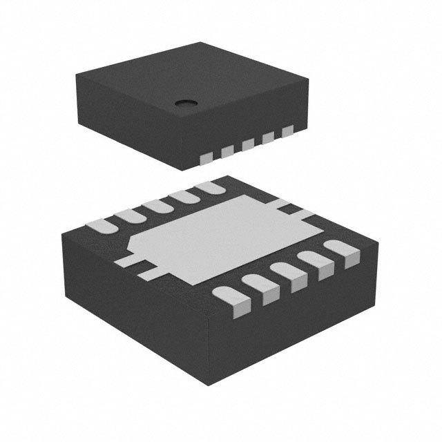
| 描述 | IC LED DRVR WT/OLED BCKLT 10-SONLED照明驱动器 Dual Output Boost WLED Driver |
| 产品分类 | |
| 品牌 | Texas Instruments |
| 产品手册 | |
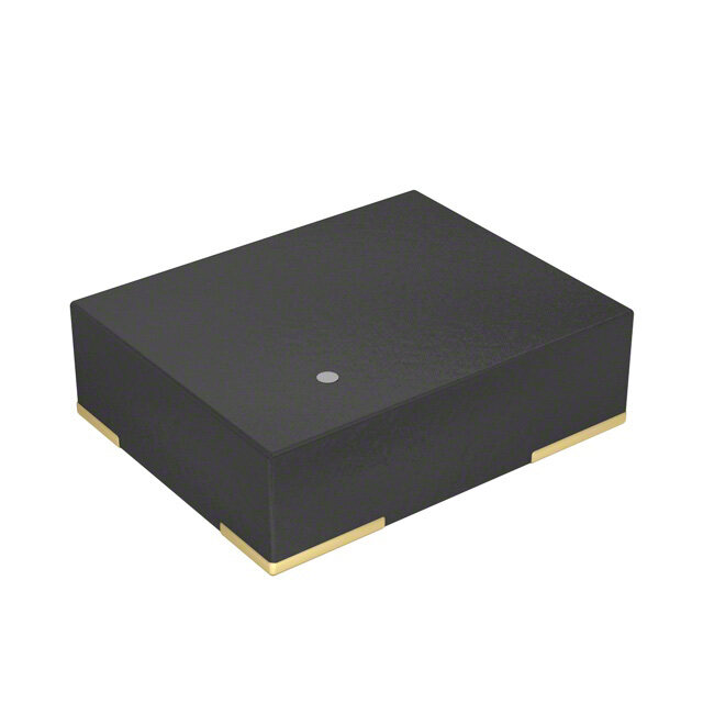
| 产品图片 |
|
| rohs | 符合RoHS无铅 / 符合限制有害物质指令(RoHS)规范要求 |
| 产品系列 | LED照明电子器件,LED照明驱动器,Texas Instruments TPS61150ADRCR- |
| 数据手册 | |
| 产品型号 | TPS61150ADRCR |
| 产品目录页面 | |
| 产品种类 | LED照明驱动器 |
| 低电平输出电流 | 34 mA |
| 供应商器件封装 | 10-SON(3x3) |
| 其它名称 | 296-21273-1 |
| 内部驱动器 | 是 |
| 功率耗散 | 370 mW |
| 包装 | 剪切带 (CT) |
| 单位重量 | 26.100 mg |
| 参考设计库 | http://designs.digikey.com/library/4294959899/4294959898/108 |
| 商标 | Texas Instruments |
| 安装类型 | 表面贴装 |
| 安装风格 | SMD/SMT |
| 封装 | Reel |
| 封装/外壳 | 10-VFDFN 裸露焊盘 |
| 封装/箱体 | VSON-10 |
| 工作温度 | -40°C ~ 85°C |
| 工作频率 | 1.2 MHz |
| 工厂包装数量 | 3000 |
| 恒压 | - |
| 恒流 | - |
| 拓扑 | PWM,升压(升压) |
| 拓扑结构 | Boost |
| 最大工作温度 | + 85 C |
| 最大电源电流 | 2 mA |
| 最小工作温度 | - 40 C |
| 标准包装 | 1 |
| 电压-电源 | 2.5 V ~ 6 V |
| 电压-输出 | 27V |
| 类型 | Inductive |
| 类型-初级 | 背光 |
| 类型-次级 | 白色 LED |
| 系列 | TPS61150A |
| 输入电压 | 2.5 V to 6 V |
| 输出数 | 2 |
| 输出电流 | 700 mA |
| 输出端数量 | 2 Output |
| 输出类型 | Current Mode |
| 配用 | /product-detail/zh/TPS61150AEVM-150/296-31226-ND/1907982/product-detail/zh/TPS61150EVM-150/296-19745-ND/1087460 |
| 频率 | 1MHz ~ 1.5MHz |


- 商务部:美国ITC正式对集成电路等产品启动337调查
- 曝三星4nm工艺存在良率问题 高通将骁龙8 Gen1或转产台积电
- 太阳诱电将投资9.5亿元在常州建新厂生产MLCC 预计2023年完工
- 英特尔发布欧洲新工厂建设计划 深化IDM 2.0 战略
- 台积电先进制程称霸业界 有大客户加持明年业绩稳了
- 达到5530亿美元!SIA预计今年全球半导体销售额将创下新高
- 英特尔拟将自动驾驶子公司Mobileye上市 估值或超500亿美元
- 三星加码芯片和SET,合并消费电子和移动部门,撤换高东真等 CEO
- 三星电子宣布重大人事变动 还合并消费电子和移动部门
- 海关总署:前11个月进口集成电路产品价值2.52万亿元 增长14.8%


.jpg)

PDF Datasheet 数据手册内容提取
TPS61150A www.ti.com SLVS706–OCTOBER2006 DUAL OUTPUT BOOST WLED DRIVER USING SINGLE INDUCTOR FEATURES The two current outputs are ideal for driving WLED • 2.5Vto6VInputVoltageRange backlight for the sub and main displays in clam shell phones.The two outputs can also be used for driving • 0.7AIntegratedSwitch display and keypad backlights. When used together, • Built-inPowerDiode the two outputs can drive up to 14 WLED for one • 1.2MHzFixedPWMFrequency largedisplay. • IndividuallyProgrammableOutputCurrent In addition to the small inductor, small capacitor and • Input-to-OutputIsolation 3mmx3mmQFN package, the built-in MOSFET and diode eliminate the need for any external power • Built-inSoftStart devices. Overall, the IC provides an extremely • 27VOvervoltageProtection compact solution with high efficiency and plenty of • 3%at15mAMatchingbetweenTwoCurrent flexibility. Strings,ImprovementfromTPS61150/1 TYPICAL APPLICATION • Upto83%Efficiency • Upto30kHzPWMDimmingFrequency 2.5V to 6V Input L1 • Availiableina10Pin,3· 3mmQFNPackage 10mH C1 1mF SW APPLICATIONS VIN IOUT • Upto14WLEDDriverforMediaFormFactor C2 GND 1mF Display • SubandMainDisplayBacklightinClamShell TPS61150A Phones SEL1 IFB1 • DisplayandKeypadBacklightinPortable SEL2 IFB2 Equipment ISET1 ISET2 DESCRIPTION R1 R2 56.5kW 56.5kW The TPS61150A is a high frequency boost converter with two regulated current outputs for driving WLEDs. Each current output can be individually programmed through external resistors. There is dedicated selection pin for each output, so the two outputs can be turned on separately or simultaneously. The output current can be reduced by a pulse width modulation (PWM) signal on the selectpinsorananalogvoltageontheISETpin.The boost regulator runs at 1.2MHz fixed switching frequency to reduce output ripple and avoid audible noisesassociatedwithPFMcontrol. Pleasebeawarethatanimportantnoticeconcerningavailability,standardwarranty,anduseincriticalapplicationsofTexas Instrumentssemiconductorproductsanddisclaimerstheretoappearsattheendofthisdatasheet. PRODUCTIONDATAinformationiscurrentasofpublicationdate. Copyright©2006,TexasInstrumentsIncorporated Products conform to specifications per the terms of the Texas Instruments standard warranty. Production processing does not necessarilyincludetestingofallparameters.
TPS61150A www.ti.com SLVS706–OCTOBER2006 Thesedeviceshavelimitedbuilt-inESDprotection.Theleadsshouldbeshortedtogetherorthedeviceplacedinconductivefoam duringstorageorhandlingtopreventelectrostaticdamagetotheMOSgates. ORDERINGINFORMATION(1) T PACKAGE OVP(Typ.) PACKAGEMARKING A –40to85(cid:176) C TPS61150ADRCR 28V BTK –40to85(cid:176) C TPS61150ADRCT 28V BTK (1) Forthemostcurrentpackageandorderinginformation,seethePackageOptionAddendumattheend ofthisdocument,orseetheTIwebsiteatwww.ti.com. DEVICE INFORMATION QFN PACKAGE (TOPVIEW) IFB1 1 10 IFB2 ISET 2 Exposed 9 ISET2 Thermal SEL1 3 Pad 8 GND SEL2 4 7 IOUT VIN 5 6 SW TERMINALFUNCTIONS TERMINAL I/O DESCRIPTION NAME NO. Inputpin.VINprovidesthecurrenttotheboostpowerstage,andalsopowerstheICcircuit.WhenVINis VIN 5 I belowtheundervoltagelockoutthreshold,theICturnsoffanddisablesoutputs;therebydisconnectingthe WLEDsfromtheinput. GND 8 O Ground.Connecttheinputandoutputcapacitorsascloseaspossibletothispin. SW 6 I SwitchingnodeoftheIC. IOUT 7 O Constantcurrentsupplyoutput.IOUTisdirectlyconnectedtotheboostconverteroutput. ReturnpathfortheIOUTregulation.Thecurrentregulatorisconnectedtothispin,anditcanbedisabled IFB1,IFB2 10 I toopenthecurrentpath. ISET1, 2 I Outputcurrentprogramming.Theresistorconnectedtothepinprogramsthecorrespondingoutputcurrent. ISET2 9 SEL1, 3 I Modeselection.SeeTable1fordetails. SEL2 4 Thethermalpadshouldbesolderedtotheanalogground.Ifpossible,usethethermalpadtoconnectto ThermalPad groundplaneforidealpowerdissipation. Table1.TPS61150AModeSelection SEL1 SEL2 IFB1 IFB2 H L Enable Disable L H Disable Enable H H Enable Enable L L ICShutdown 2 SubmitDocumentationFeedback
TPS61150A www.ti.com SLVS706–OCTOBER2006 FUNCTIONALBLOCKDIAGRAM SW IOUT VIN + − 1.2MHz Current Mode Control GND PWM IFB1 SEL1 Current Sink 0.33V ISET1 Error Amplifier IFB2 TPS61150A SEL2 Current Sink ISET2 ABSOLUTE MAXIMUM RATINGS(1) overoperatingfree-airtemperaturerange(unlessotherwisenoted) VALUE UNIT SupplyvoltagesonpinVIN(2) –0.3to7 V VoltagesonpinsSEL1/2,ISET1/2(2) –0.3to7 V VoltageonpinIOUT,SW,IFB1andIFB2(2) 30 V Continuouspowerdissipation SeeDissipationRatingTable Operatingjunctiontemperaturerange –40to150 (cid:176) C Storagetemperaturerange –65to150 (cid:176) C LeadTemperature(soldering,10sec) 260 (cid:176) C (1) Stressesbeyondthoselistedunderabsolutemaximumratingsmaycausepermanentdamagetothedevice.Thesearestressratings only,andfunctionaloperationofthedeviceattheseoranyotherconditionsbeyondthoseindicatedunderrecommendedoperating conditionsisnotimplied.Exposuretoabsolute-maximum-ratedconditionsforextendedperiodsmayaffectdevicereliability. (2) Allvoltagevaluesarewithrespecttonetworkgroundterminal. DISSIPATION RATINGS T £ 25(cid:176) C T =70(cid:176) C T =85(cid:176) C PACKAGE Rq JA POWEARRATING POWAERRATING POWAERRATING QFN (1) 270oC/W 370mW 204mW 148mW QFN(2)(2 48.7oC/W 2.05W 1.13W 821mW (1) SolderedPowerPADonastandard2-layerPCBwithoutviasforthermalpad. (2) SolderedPowerPADonastandard4-layerPCBwithviasforthermalpad. SubmitDocumentationFeedback 3
TPS61150A www.ti.com SLVS706–OCTOBER2006 RECOMMENDED OPERATING CONDITIONS overoperatingfree-airtemperaturerange(unlessotherwisenoted) MIN NOM MAX UNIT V Inputvoltagerange 2.5 6.0 V I V Outputvoltagerange VIN 27 V O L Inductor(1) 10 m H C Inputcapacitor(1) 1 m F I C Outputcapacitor(1) 1 m F O T Operatingambienttemperature –40 85 (cid:176) C A T Operatingjunctiontemperature –40 125 (cid:176) C J (1) SeeApplicationSectionforfurtherinformation. 4 SubmitDocumentationFeedback
TPS61150A www.ti.com SLVS706–OCTOBER2006 ELECTRICAL CHARACTERISTICS VIN=3.6V,SELx=VIN,Rset=80kW ,V =15V,T =–40(cid:176) Cto85(cid:176) C,typicalvaluesareatT =25(cid:176) C(unlessotherwise (IOUT) A A noted) PARAMETER TESTCONDITIONS MIN TYP MAX UNIT SUPPLYCURRENT V Inputvoltagerange 2.5 6.0 V I I OperatingquiescentcurrentintoVIN DevicePWMswitchingnoload 2 mA Q I Shutdowncurrent SELx=GND,T =25(cid:176) C 1.7 1.9 m A SD A SELx=GND 2.7 3 V Under-voltagelockoutthreshold VINfalling 1.65 1.8 V UVLO V Under-voltagelockouthysterisis 70 mV hys ENABLEANDSOFTSTART V SELlogichighvoltage V =2.5Vto6V 1.2 V (selh) I V SELlogiclowvoltage V =2.5Vto6V 0.4 V (sell) I R SELpulldownresistor 300 700 kW (en) t SELpulsewidthtodisable SELxhightolow 40 ms (off) I IFBsoftstartcurrentsteps 16 (ss) t Softstarttimestep Measuredasclockdivider 64 (ss) t Softstartenabletime Timebetweenfallingandrisingoftwoadjacent 40 ms (ss_en) SELxpulses CURRENTFEEDBACK V ISETpinvoltage 1.204 1.229 1.254 V (ISET) K Currentmultipler,I /I ,I /I ISETcurrent=16.7m A 883 920 957 ISET fb1 set1 fb2 set2 ISETcurrent=1.2m A 736 920 1104 K Currentmatching,(2· |I –I |)/(I +I ) ISETcurrent=16.7m A 0% 3% M fb1 fb2 fb1 fb2 ISETcurrent=1.2m A 0% 20% V IFBregulationvoltage 300 330 360 mV (IFB) V IFBlowthresholdhysteresis 60 mV hys(IFB_L) t Currentsinksettletimemeasuredfrom 6 m s I(sink) SELxrisingedge(1) I IFBpinleakagecurrent IFBvoltage=25V 1 m A lkg POWERSWITCHANDDIODE R N-channelMOSFETon-resistance V =V =3.6V 0.6 0.9 W DS(ON) IN GS I N-channelleakagecurrent V =25V 1 m A lkg(N_NFET) DS V Powerdiodeforwardvoltage Diodecurrent=0.7A 0.83 1.0 V (F) OCANDOVP Dualoutput,IOUT=15V,Dutycycle=76% 0.75 1.0 1.25 I N-ChannelMOSFETcurrentlimit A L Singleoutput,IOUT=15V,Dutycycle=76% 0.40 0.55 0.7 I Currentsinkmaxoutputcurrent IFBcurrent=330mV 34 mA (IFB_MAX) V Overvoltagethreshold 27 28 29 V ovp V Overvoltagehysteresis 550 mV ovp_hys PWMANDPFMCONTROL F Oscillatorfrequency 1.0 1.2 1.5 MHz S D Maximumdutycycle Feedbackvoltage=1.0V 89% 93% max THERMALSHUTDOWN T Thermalshutdownthreshold 160 (cid:176) C shutdown T Thermalshutdownthresholdhysteresis 15 (cid:176) C hys (1) ThisspecificationdeterminestheminimumontimerequiredforPWMdimmingfordesirablelinearity.ThemaximumPWMdimming frequencycanbecalculatedfromtheminimumdutycyclerequiredintheapplication. SubmitDocumentationFeedback 5
TPS61150A www.ti.com SLVS706–OCTOBER2006 TYPICAL CHARACTERISTICS Table of Graphs FIGURES OvercurrentLimit VIN=3.0V,3.6V,and4.2V,singleanddualoutput 1,2 WLEDefficiency VIN=3.3V,3.6Vand4.2V,3WLED,WLEDvoltage=11V 3 WLEDefficiency VIN=3.3V,3.6Vand4.2V,4WLED,WLEDvoltage=15V 4 WLEDefficiency VIN=3.3V,3.6Vand4.2V,5WLED,WLEDvoltage=19V 5 WLEDefficiency VIN=3.3V,3.6Vand4.2V,6WLED,WLEDvoltage=23V 6 Bothonefficiency VIN=3.3V,3.6Vand4.2V,4WLEDoneachoutput 7 Kvalueovercurrent VIN=3.6V,I =1mAto25mA 8 WLED PWMdimminglinearity Frequency=20kHzand30kHz 9 SingleoutputPWMdimmingwaveform 10 MultiplexedPWMdimmingwaveform 11 Startupwaveform 12 OVERCURRENTLIMIT(SINGLEOUTPUT) OVERCURRENTLIMIT(DUALOUTPUT) vs vs DUTYCYCLE DUTYCYCLE 600 1200 VI= 4.2V VI = 3V 500 1000 V = 3.6V I A 400 A 800 m m V = 3.6V mit - VI= 3V mit - I Li 300 Li 600 VI= 4.2V nt nt e e urr urr C 200 C 400 100 200 0 0 10 20 30 40 50 60 70 80 90 10 20 30 40 50 60 70 80 90 Duty Cycle - % Duty Cycle - % Figure1. Figure2. 6 SubmitDocumentationFeedback
TPS61150A www.ti.com SLVS706–OCTOBER2006 EFFICIENCY EFFICIENCY vs vs LOADCURRENT LOADCURRENT 90 90 WLED Voltage = 11V, 3 WLED, WLED Voltage = 15V, 4 WLED, Single Output Single Output V = 3.6V 80 I 80 V = 4.2V I % % ncy - 70 VI= 3.3V ncy - 70 VI= 3.3V e e ci ci V = 3.6V Effi Effi I 60 60 V = 4.2V I 50 50 0 5 10 15 20 25 0 5 10 15 20 25 WLED Current - mA WLED Current - mA Figure3. Figure4. EFFICIENCY EFFICIENCY vs vs LOADCURRENT LOADCURRENT 90 90 WLED Voltage = 19V, 5 WLED, WLED Voltage = 23V, 6 WLED, Single Output Single Output V = 4.2V 80 I 80 VI= 4.2V % % Efficiency - 70 VI= 3.3VVI= 3.6V Efficiency - 70 VI= 3.3VVI= 3.6V 60 60 50 50 0 5 10 15 20 25 0 5 10 15 20 25 WLED Current - mA WLED Current - mA Figure5. Figure6. SubmitDocumentationFeedback 7
TPS61150A www.ti.com SLVS706–OCTOBER2006 BOTHONEFFICIENCY KVALUE vs vs TOTALOUTPUTCURRENT WLEDCURRENT 90 1200 WLED1 Voltage = 15V V = 3.6V I WLED2 Voltage = 15V WLED1 Voltage = 15V WLED2 Voltage = 15V 1100 80 % VI= 3.3V 1000 ncy - 70 VI= 3.6V alue WLED1 cie VI= 4.2V K V Effi 900 WLED2 60 800 50 700 0 10 20 30 40 50 60 0 10 20 30 40 50 IO- Total Output Current - mA WLED Current - mA Figure7. Figure8. SINGLEOUTPUTWLEDPWM WLEDBRIGHTNESSDIMMINGLINEARITY BRIGHTNESSDIMMING 25 ISEL2 20 5V/div, DC A SW m nt - 15 10V/div, DC e rr IOUT u c D 1V/div, DC E 10 WL 15V Offset WLED Current f = 20kHz 20mA/div, DC 5 t - Time - 20ms/div f = 30kHz 0 0 20 40 60 80 100 PWM Duty cycle - % Figure9. Figure10. 8 SubmitDocumentationFeedback
TPS61150A www.ti.com SLVS706–OCTOBER2006 MULTIPLEXEDPWMDIMMING (ISEL1:4WLED,ISEL2:2WLED) WLEDSTARTUP ISEL1 ISEL2 5V/div, DC ISEL2 5V/div, DC IOUT 10V/div, DC 5V/div, DC Inductor Current 500mA/div, DC IOUT WLED Current 20mA/div, DC 5V/div, DC t - Time - 200ms/div t - Time - 2ms/div Figure11. Figure12. SubmitDocumentationFeedback 9
TPS61150A www.ti.com SLVS706–OCTOBER2006 DETAILED DESCRIPTION CURRENT REGULATION The TPS61150A uses a single boost regulator to drive 2 WLED strings whose current can be programmed independently. The boost converter adopts PWM control which is ideal for high output current and low output ripple noises. The feedback loop regulates the IFB pin to a threshold voltage (330mV typical), giving the current sinkcircuitjustenoughheadroomtooperate. TheregulationcurrentissetbytheresistorontheIsetpinbasedon V I (cid:2) ISET(cid:1)K O R ISET SET (1) where I =outputcurrent O V =Isetpinvoltage(1.229Vtypical) ISET R =Isetpinresistorvalue SET K =currentmultiplier(920typical) ISET When both outputs are enabled, the boost converter regulates to the IFB pin that demands higher Iout pin voltage, V , and let the other IFB pin rise above its regulation voltage. The feedback path dynamically (IOUT) switches to the other IFB pin if its voltage drops more than the IFB low hysterisis (60mV typical) below it's regulation voltage. This ensures proper current regulation for both outputs. When both IFB voltages are low, IFB1 is used for regulation. Once IFB1 reaches its regulation voltage, the feedback path may hand over to IFB2 ifitisstilllow,andtheboostoutputwillcontinuetorise. The overall efficiency in this mode depends on the voltage different between the IFB1 and IFB2. A large difference reduces the efficiency due to power losses across the current sink circuit. To improve the efficiency of the both-on mode, the two current outputs can be turned on complimentarily by applying out of phase enable signal to the SEL pins. The ISET pin resistors need to be recalculated to compensate for the reduced DC current. START UP During start up, both the boost converter and the current sink circuitry are trying to establish steady state simultaneously. The current sink circuitry ramps up current in 16 steps, with each step taking 64 clock cycles. This ensures that the current sink loop is slower than the boost converter response during startup. Therefore, the boost converter output comes up slowly as current sink circuitry ramps up the current. This ensures smooth startupandminimizesin-rushcurrent. OVERVOLTAGE PROTECTION To prevent the boost output run away as the result of WLED disconnection, there is an overvoltage protection circuit which stops the boost converter from switching as soon as its output exceeds the OVP threshold. When the voltage falls below the OVP threshold, the converter resumes switching. TPS61150A provides 28V(typical) OVPtopreventa25Vratedoutputcapacitorortheinternal30VFETfrombreakingdown. UNDERVOLTAGE LOCKOUT An undervoltage lockout prevents mis-operation of the device for input voltages below 1.65V (typical). When the input voltage is below the undervoltage threshold, the device remains off and both the boost converter and currentsinkcircuitareturnedoff,providingisolationbetweeninputandoutput. THERMAL SHUTDOWN An internal thermal shutdown turns off the IC when the typical junction temperature of 160(cid:176) C is exceeded. The thermalshutdownhasahysteresisoftypically15(cid:176) C. 10 SubmitDocumentationFeedback
TPS61150A www.ti.com SLVS706–OCTOBER2006 DETAILED DESCRIPTION (continued) ENABLE Pulling either the SEL1 or SEL2 pin low turns off the corresponding output. If both SEL1 and SEL2 are low for more than 40ms, the IC shuts down and consumes less than 2m A (room temperature) current. The SEL pin can also be used for PWM brightness dimming. To improve PWM dimming linearity, soft start is disabled if the time between falling and rising edges of two adjacent SELx pulses is less than 40ms. See APPLICATION INFORMATIONfordetails. EachSELinputpinhasaninternalpulldownresistortodisablethedevicewhenthepinisfloating. SubmitDocumentationFeedback 11
TPS61150A www.ti.com SLVS706–OCTOBER2006 APPLICATION INFORMATION MAXIMUM OUTPUT CURRENT Theover-currentlimitinaboostconverterlimits the maximum input current and thus maximum input power for a given input voltage. Maximum output power is less than maximum input power due to power conversion losses. Therefore, the current limit, input voltage, output voltage and efficiency can all change maximum current output. Since current limit clamps peak inductor current, ripple has to be subtracted to derive maximum DC current. The ripple current is a function of switching frequency, inductor value and duty cycle. The following equations take intoaccountofalltheabovefactorsformaximumoutputcurrentcalculation. 1 Ip(cid:4) (cid:5)L(cid:1)(cid:7) 1 (cid:2) 1 (cid:8)(cid:1)Fs(cid:6) Viout(cid:2)Vf(cid:3)Vin Vin (2) where Ip=inductorpeak-to-peakripple L=inductorvalue Vf=powerdiodeforwardvoltage Fs=switchingfrequency Viout=boostoutputvoltage.Itisequalto330mV+voltagedropacrossWLED. (cid:4) Ip(cid:5) Vin(cid:1) Ilim(cid:2)2 (cid:1)(cid:1) Iout_max(cid:3) Viout (3) where Iout_max=maximumoutputcurrentoftheboostconverter Ilim=overcurrentlimit h =efficiency To keep a tight range of the overcurrent limit, The TPS61150A uses the Vin and Iout pin voltage to compensate for the overcurrent limit variation caused by the slope compensation. However, the current threshold still has residual dependency on the VIN and IOUT voltage. Use Figure 1 and Figure 2 to identify the typical overcurrent limitinyourapplication,anduse– 25%tolerancetoaccountfortemperaturedependencyandprocessvariations. The maximum output current can also be limited by the current capability of the current sink circuitry. It is designedtoprovidemaximum35mAcurrentregardlessofthecurrentcapabilityoftheboostconverter. WLED BRIGHTNESS DIMMING There are three ways to change the output current on the fly for WLED dimming. The first method parallels an additional resistor with the ISET pin resistor as shown in Figure 13 . The switch (Q1) can change the ISET pin resistance and therefore, modify the output current. This method is very simple, but can only provide limited dimmingsteps. ISET R1 RISET Q1 ON/OFF Logic Figure13.SwitchingIn/OutanAdditionalResistortoChangeOutputCurrent 12 SubmitDocumentationFeedback
TPS61150A www.ti.com SLVS706–OCTOBER2006 APPLICATION INFORMATION (continued) Alternatively, a PWM dimming signal at the SEL pin can modulate the output current by the duty cycle of the signal. The logic high of the signal turns on the current sink circuit, while the logic low turns it off. This operation creates an averaged DC output current proportional to the duty cycle of the PWM signal. The frequency of the PWM signal has to be high enough to avoid flashing of the WLEDs. The soft start of the current sink circuit is disabledduringthePWMdimmingtoimprovelinearity. The major concern of the PWM dimming is the creation of audible noises which can come from the inductor and/or output capacitor of the boost converter. The audible noises on the output capacitor are created by the presence of voltage ripple in range of audible frequencies. The TPS61150A alleviates the problem by disconnecting the WLEDs from the output capacitor when the SEL pin is low. Therefore, the output capacitor is notdischargedbytheWLEDs,whichreducesthevoltagerippleduringPWMdimming. The audible noises can be eliminated by using PWM dimming frequency above or below the audible frequency range. The maximum PWM dimming frequency of the TPS61150A is determined by the current settling time (t ) which is the time required for the circuit sink circuit to reach steady state after the SEL pin transitions from isink lowtohigh.Themaximumdimmingfrequencycanbecalculatedby D F (cid:1) min PWM_MAX T isink (4) D =mindutycycleofthePWMdimmingrequiredintheapplication. min For 20% D , PWM dimming frequency up to 33kHz is possible, making the noise frequency above the audible min range. The third method uses an external DC voltage and resistor as shown in Figure 14 to change the ISET pin current, and thus control the output current. The DC voltage can be the output of a filtered PWM signal. The equationtocalculatetheoutputcurrentis (cid:5)1.229 1.229(cid:3)VDC(cid:6) IWLED(cid:4)KISET(cid:1) R (cid:2) R for DCvoltageinput ISET 1 (5) (cid:5)1.229 1.229(cid:3)VDC(cid:6) IWLED(cid:4)KISET(cid:1) RISET(cid:2) R1(cid:2)10K for PWMsignalinput (6) K =currentmultiplierbetweentheISETpincurrentandtheIFBpincurrent. ISET VDC=voltageoftheDCvoltagesourceortheDCvoltageofthePWMsignal. ISET ISET Filter PWM Signal DC Voltage R1 10 k(cid:1) R1 RISET 0.1 (cid:2)F RISET Figure14.AnalogDimmingUsesanExternalVoltageSourcetoControltheOutputCurrent INDUCTOR SELECTION Because the selection of the inductor affects power supplies steady state operation, transient behavior, and loop stability, the inductor is the most important component in power regulator design. There are three specifications most important to the performance of the inductor, inductor value, DC resistance, and saturation current. Consideringinductorvaluealoneisnotenough. The inductors inductance value determines the inductor ripple current. It is generally recommended to set peak-to-peak ripple current given by Equation 2 to 30–40% of DC current. It is a good compromise of power losses and inductor size. For this reason, 10m H inductors are recommended for TPS61150A. Inductor DC currentcanbecalculatedas SubmitDocumentationFeedback 13
TPS61150A www.ti.com SLVS706–OCTOBER2006 APPLICATION INFORMATION (continued) V (cid:1)I I (cid:2) iout out L_DC V (cid:1)(cid:1) in (7) UsethemaximumloadcurrentandminimumV forcalculation. I The internal loop compensation for PWM control is optimized for the external component shown in the typical application circuit with consideration of component tolerance. Inductor values can have – 20% tolerance with no current bias. When the inductor current approaches saturation level, its inductance can decrease 20 to 35% from the 0A value depending on how the inductor vendor defines saturation. Using an inductor with a smaller inductance value forces discontinuous PWM in which inductor current ramps down to zero before the end of each switching cycle. It reduces the boost converter’s maximum output current, and causes large input voltage ripple. An inductor with larger inductance reduces the gain and phase margin of the feedback loop, possibly resultingininstability Regulator efficiency is dependent on the resistance of its high current path and switching losses associated with the PWM switch and power diode. Although the TPS61150A has optimized the internal switches, the overall efficiency still relies on inductors DC resistance (DCR); Lower DCR improves efficiency. However, there is a trade off between DCR and inductor size, and shielded inductors typically have higher DCR than unshielded ones. DCR in range of 150mW to 350mW is suitable for applications requiring both on mode. DCR is the range of 250mW to 450mW is a good choice for single output application. Table 2 and Table 3 list recommended inductormodels. Table2.RecommendedInductorsforSingleOutput L DCRTyp Isat SIZE (m H) (mW ) (A) (L· W· Hmm) TDK VLF3012AT-100MR49 10 360 0.49 2.8· 3.0· 1.2 VLCF4018T-100MR74-2 10 163 0.74 4.0· 4.0· 1.8 Sumida CDRH2D11/HP 10 447 0.52 3.2· 3.2· 1.2 CDRH3D16/HP 10 230 0.84 4.0· 4.0· 1.8 Table3.RecommendedInductorsforDualOutput L DCRTyp Isat SIZE (m H) (mW ) (A) (L· W· Hmm) TDK VLCF4018T-100MR74-2 10 163 0.74 4.0· 4.0· 1.8 VLF4012AT-100MR79 10 300 0.85 3.5· 3.7· 1.2 Sumida CDRH3D16/HP 10 230 0.84 4.0· 4.0· 1.8 CDRH4D11/HP 10 340 0.85 4.8· 4.8· 1.2 INPUT AND OUTPUT CAPACITOR SELECTION Theoutputcapacitorismainlyselectedfortheoutputrippleoftheconverter.Thisripplevoltageisthesumof the ripple caused by the capacitor’s capacitance and its equivalent series resistance (ESR). Assuming a capacitor withzeroESR,theminimumcapacitanceneededforagivenripplecanbecalculatedby (cid:4)Viout(cid:2)Vin(cid:5)Iout Cout(cid:3)Viout(cid:1)Fs(cid:1)Vripple (8) V =Peak-to-peakoutputripple. ripple 14 SubmitDocumentationFeedback
TPS61150A www.ti.com SLVS706–OCTOBER2006 For V = 3.6V, V = 20V, and F = 1.2MHz, 0.1% ripple (20mV) would require 1.0m F capacitor. For this value, I iout s ceramiccapacitorsarethebestchoiceforitssize,costandavailability. TheadditionaloutputripplecomponentcausedbyESRiscalculatedusing: V =I · R ripple_ESR out ESR Due to it's low ESR, V can be neglected for ceramic capacitors, but must be considered if tantalum or ripple_ESR electrolyticcapacitorsareused. During a load transient, the capacitor at the output of the boost converter has to supply or absorb additional current before the inductor current ramps up the steady state value. Larger capacitors always help to reduce the voltageoverandundershootduringaloadtransient.Alargercapacitoralsohelpsloopstability. Care must be taken when evaluating a ceramic capacitor’s derating due to applied dc voltage, aging and frequency response. For example, larger form factor capacitors (in 1206 size) have their self-resonant frequencies in the range of TPS61150A’s switching frequency, so the effective capacitance is significantly lower. Therefore,itmaybenecessarytousesmallcapacitorsinparallelinsteadofonelargecapacitor. Thepopularvendorsforhighvalueceramiccapacitorsare: TDK(http://www.component.tdk.com/components.php) Murata(http://www.murata.com/cap/index.html) Table4.RecommendedInputandOutputCapacitors Capacitance(m F) Voltage(V) Case TDK C3216X5R1E475K 4.7 25 1206 C2012X5R1E105K 1 25 805 C1005X5R0J105K 1 6.3 402 Murata GRM319R61E475KA12D 4.7 25 1206 GRM216R61E105KA12D 1 25 805 GRM155R60J105KE19D 1 6.3 402 LAYOUT CONSIDERATION Asforallswitching power supplies, especially those providing high current and using high switching frequencies, layout is an important design step. If layout is not carefully done, the regulator could show instability as well as EMI problems, therefore, use wide and short traces for high current paths. The input capacitor needs not only to be close to the VIN pin, but also to the GND pin in order to reduce the input ripple seen by the IC. The VIN and SW pins are conveniently located on the edges of the IC, therefore the inductor can be placed close to the IC. Theoutputcapacitorneedstobeplacedneartheloadtominimizerippleandmaximizetransientperformance. It is also beneficial to have the ground of the output capacitor close to the GND pin since there will be large ground return current flowing between them. When laying out signal ground, it is recommended to use short tracesseparatedfrompowergroundtraces,andconnectthemtogetheratasinglepoint. SubmitDocumentationFeedback 15
TPS61150A www.ti.com SLVS706–OCTOBER2006 ADDITIONAL APPLICATION CIRCUIT VIN L1 10mH C2 1mF VIN SW IOUT C2 1mF GND EN/PWM Dimming SEL1 SEL2 IFB1 IFB2 ISET1 ISET2 R1 R2 Figure15.DrivingUpto12WLEDsWithOneLCDBacklight Display Keypad VIN L1 10mH IFB1 IFB1 C1 ON ON 1mF VIN SWIOUT SEL1 GND C2 1mF IFB2 IFB2 SEL1 ON ON SEL2 IFB1 SEL2 IFB2 IC 40ms Shutdown ISET1 ISET2 R1 R2 Figure16.DrivingaKeypadandLCDBacklightbyapplyinginterleavedPWMsignaltotheSEL1and SEL2pins.ThedutycycleofthePWMsignalcontrolsbrightnessdimming 16 SubmitDocumentationFeedback
PACKAGE OPTION ADDENDUM www.ti.com 6-Feb-2020 PACKAGING INFORMATION Orderable Device Status Package Type Package Pins Package Eco Plan Lead/Ball Finish MSL Peak Temp Op Temp (°C) Device Marking Samples (1) Drawing Qty (2) (6) (3) (4/5) TPS61150ADRCR ACTIVE VSON DRC 10 3000 Green (RoHS NIPDAU Level-2-260C-1 YEAR -40 to 85 BTK & no Sb/Br) TPS61150ADRCT ACTIVE VSON DRC 10 250 Green (RoHS NIPDAU Level-2-260C-1 YEAR -40 to 85 BTK & no Sb/Br) TPS61150ADRCTG4 ACTIVE VSON DRC 10 250 Green (RoHS NIPDAU Level-2-260C-1 YEAR -40 to 85 BTK & no Sb/Br) (1) The marketing status values are defined as follows: ACTIVE: Product device recommended for new designs. LIFEBUY: TI has announced that the device will be discontinued, and a lifetime-buy period is in effect. NRND: Not recommended for new designs. Device is in production to support existing customers, but TI does not recommend using this part in a new design. PREVIEW: Device has been announced but is not in production. Samples may or may not be available. OBSOLETE: TI has discontinued the production of the device. (2) RoHS: TI defines "RoHS" to mean semiconductor products that are compliant with the current EU RoHS requirements for all 10 RoHS substances, including the requirement that RoHS substance do not exceed 0.1% by weight in homogeneous materials. Where designed to be soldered at high temperatures, "RoHS" products are suitable for use in specified lead-free processes. TI may reference these types of products as "Pb-Free". RoHS Exempt: TI defines "RoHS Exempt" to mean products that contain lead but are compliant with EU RoHS pursuant to a specific EU RoHS exemption. Green: TI defines "Green" to mean the content of Chlorine (Cl) and Bromine (Br) based flame retardants meet JS709B low halogen requirements of <=1000ppm threshold. Antimony trioxide based flame retardants must also meet the <=1000ppm threshold requirement. (3) MSL, Peak Temp. - The Moisture Sensitivity Level rating according to the JEDEC industry standard classifications, and peak solder temperature. (4) There may be additional marking, which relates to the logo, the lot trace code information, or the environmental category on the device. (5) Multiple Device Markings will be inside parentheses. Only one Device Marking contained in parentheses and separated by a "~" will appear on a device. If a line is indented then it is a continuation of the previous line and the two combined represent the entire Device Marking for that device. (6) Lead/Ball Finish - Orderable Devices may have multiple material finish options. Finish options are separated by a vertical ruled line. Lead/Ball Finish values may wrap to two lines if the finish value exceeds the maximum column width. Important Information and Disclaimer:The information provided on this page represents TI's knowledge and belief as of the date that it is provided. TI bases its knowledge and belief on information provided by third parties, and makes no representation or warranty as to the accuracy of such information. Efforts are underway to better integrate information from third parties. TI has taken and continues to take reasonable steps to provide representative and accurate information but may not have conducted destructive testing or chemical analysis on incoming materials and chemicals. TI and TI suppliers consider certain information to be proprietary, and thus CAS numbers and other limited information may not be available for release. Addendum-Page 1
PACKAGE OPTION ADDENDUM www.ti.com 6-Feb-2020 In no event shall TI's liability arising out of such information exceed the total purchase price of the TI part(s) at issue in this document sold by TI to Customer on an annual basis. Addendum-Page 2
PACKAGE MATERIALS INFORMATION www.ti.com 1-Oct-2014 TAPE AND REEL INFORMATION *Alldimensionsarenominal Device Package Package Pins SPQ Reel Reel A0 B0 K0 P1 W Pin1 Type Drawing Diameter Width (mm) (mm) (mm) (mm) (mm) Quadrant (mm) W1(mm) TPS61150ADRCR VSON DRC 10 3000 330.0 12.4 3.3 3.3 1.1 8.0 12.0 Q2 TPS61150ADRCT VSON DRC 10 250 180.0 12.4 3.3 3.3 1.1 8.0 12.0 Q2 PackMaterials-Page1
PACKAGE MATERIALS INFORMATION www.ti.com 1-Oct-2014 *Alldimensionsarenominal Device PackageType PackageDrawing Pins SPQ Length(mm) Width(mm) Height(mm) TPS61150ADRCR VSON DRC 10 3000 367.0 367.0 35.0 TPS61150ADRCT VSON DRC 10 250 210.0 185.0 35.0 PackMaterials-Page2
GENERIC PACKAGE VIEW DRC 10 VSON - 1 mm max height PLASTIC SMALL OUTLINE - NO LEAD Images above are just a representation of the package family, actual package may vary. Refer to the product data sheet for package details. 4204102-3/M
PACKAGE OUTLINE DRC0010J VSON - 1 mm max height SCALE 4.000 PLASTIC SMALL OUTLINE - NO LEAD 3.1 B A 2.9 PIN 1 INDEX AREA 3.1 2.9 1.0 C 0.8 SEATING PLANE 0.05 0.00 0.08 C 1.65 0.1 2X (0.5) (0.2) TYP EXPOSED 4X (0.25) THERMAL PAD 5 6 2X 11 SYMM 2 2.4 0.1 10 1 8X 0.5 0.30 10X 0.18 PIN 1 ID SYMM 0.1 C A B (OPTIONAL) 0.5 0.05 C 10X 0.3 4218878/B 07/2018 NOTES: 1. All linear dimensions are in millimeters. Any dimensions in parenthesis are for reference only. Dimensioning and tolerancing per ASME Y14.5M. 2. This drawing is subject to change without notice. 3. The package thermal pad must be soldered to the printed circuit board for optimal thermal and mechanical performance. www.ti.com
EXAMPLE BOARD LAYOUT DRC0010J VSON - 1 mm max height PLASTIC SMALL OUTLINE - NO LEAD (1.65) (0.5) 10X (0.6) 1 10 10X (0.24) 11 SYMM (2.4) (3.4) (0.95) 8X (0.5) 6 5 (R0.05) TYP ( 0.2) VIA TYP (0.25) (0.575) SYMM (2.8) LAND PATTERN EXAMPLE EXPOSED METAL SHOWN SCALE:20X 0.07 MIN 0.07 MAX EXPOSED METAL ALL AROUND ALL AROUND EXPOSED METAL SOLDER MASK METAL METAL UNDER SOLDER MASK OPENING SOLDER MASK OPENING NON SOLDER MASK SOLDER MASK DEFINED DEFINED (PREFERRED) SOLDER MASK DETAILS 4218878/B 07/2018 NOTES: (continued) 4. This package is designed to be soldered to a thermal pad on the board. For more information, see Texas Instruments literature number SLUA271 (www.ti.com/lit/slua271). 5. Vias are optional depending on application, refer to device data sheet. If any vias are implemented, refer to their locations shown on this view. It is recommended that vias under paste be filled, plugged or tented. www.ti.com
EXAMPLE STENCIL DESIGN DRC0010J VSON - 1 mm max height PLASTIC SMALL OUTLINE - NO LEAD 2X (1.5) (0.5) SYMM EXPOSED METAL 11 TYP 10X (0.6) 1 10 (1.53) 10X (0.24) 2X (1.06) SYMM (0.63) 8X (0.5) 6 5 (R0.05) TYP 4X (0.34) 4X (0.25) (2.8) SOLDER PASTE EXAMPLE BASED ON 0.125 mm THICK STENCIL EXPOSED PAD 11: 80% PRINTED SOLDER COVERAGE BY AREA SCALE:25X 4218878/B 07/2018 NOTES: (continued) 6. Laser cutting apertures with trapezoidal walls and rounded corners may offer better paste release. IPC-7525 may have alternate design recommendations. www.ti.com
IMPORTANTNOTICEANDDISCLAIMER TI PROVIDES TECHNICAL AND RELIABILITY DATA (INCLUDING DATASHEETS), DESIGN RESOURCES (INCLUDING REFERENCE DESIGNS), APPLICATION OR OTHER DESIGN ADVICE, WEB TOOLS, SAFETY INFORMATION, AND OTHER RESOURCES “AS IS” AND WITH ALL FAULTS, AND DISCLAIMS ALL WARRANTIES, EXPRESS AND IMPLIED, INCLUDING WITHOUT LIMITATION ANY IMPLIED WARRANTIES OF MERCHANTABILITY, FITNESS FOR A PARTICULAR PURPOSE OR NON-INFRINGEMENT OF THIRD PARTY INTELLECTUAL PROPERTY RIGHTS. These resources are intended for skilled developers designing with TI products. You are solely responsible for (1) selecting the appropriate TI products for your application, (2) designing, validating and testing your application, and (3) ensuring your application meets applicable standards, and any other safety, security, or other requirements. These resources are subject to change without notice. TI grants you permission to use these resources only for development of an application that uses the TI products described in the resource. Other reproduction and display of these resources is prohibited. No license is granted to any other TI intellectual property right or to any third party intellectual property right. TI disclaims responsibility for, and you will fully indemnify TI and its representatives against, any claims, damages, costs, losses, and liabilities arising out of your use of these resources. TI’s products are provided subject to TI’s Terms of Sale (www.ti.com/legal/termsofsale.html) or other applicable terms available either on ti.com or provided in conjunction with such TI products. TI’s provision of these resources does not expand or otherwise alter TI’s applicable warranties or warranty disclaimers for TI products. Mailing Address: Texas Instruments, Post Office Box 655303, Dallas, Texas 75265 Copyright © 2020, Texas Instruments Incorporated