ICGOO在线商城 > 集成电路(IC) > PMIC - 稳压器 - DC DC 开关稳压器 > TPS61087DRCR
 Datasheet下载
- 型号: TPS61087DRCR
- 制造商: Texas Instruments
- 库位|库存: xxxx|xxxx
- 要求:
| 数量阶梯 | 香港交货 | 国内含税 |
| +xxxx | $xxxx | ¥xxxx |
查看当月历史价格
查看今年历史价格
TPS61087DRCR产品简介:
ICGOO电子元器件商城为您提供TPS61087DRCR由Texas Instruments设计生产,在icgoo商城现货销售,并且可以通过原厂、代理商等渠道进行代购。 TPS61087DRCR价格参考。Texas InstrumentsTPS61087DRCR封装/规格:PMIC - 稳压器 - DC DC 开关稳压器, Boost Switching Regulator IC Positive Adjustable 3V 1 Output 3.2A (Switch) 10-VFDFN Exposed Pad。您可以下载TPS61087DRCR参考资料、Datasheet数据手册功能说明书,资料中有TPS61087DRCR 详细功能的应用电路图电压和使用方法及教程。
TPS61087DRCR是Texas Instruments(德州仪器)推出的一款高效、同步升压型DC-DC开关稳压器,适用于需要从较低输入电压提升至较高稳定输出电压的应用场景。其典型应用场景包括便携式设备、电池供电系统和需要多路电源轨的电子产品。

该器件支持2.3V至5.5V的宽输入电压范围,可提供最高达5.5V的可调输出电压,输出电流能力高达1.4A(开关电流限制),非常适合由单节锂电池或USB电源供电的系统。由于其采用同步整流技术,转换效率高达96%,有效降低功耗,延长电池续航时间。

常见应用包括:智能手机、平板电脑、手持终端、移动电源(充电宝)、便携式医疗设备、数码相机以及LED背光驱动电路等。此外,它也广泛用于工业手持设备、无线传感器节点和小型无线模块(如Wi-Fi、蓝牙模块)中,为系统中的微处理器、存储器或传感器提供稳定的电源。

TPS61087DRCR采用小尺寸6引脚SON封装(DRC),占用PCB面积小,适合空间受限的高密度设计。同时具备过温保护、过流保护和软启动功能,提高了系统的可靠性与安全性。因其高集成度、高效率和良好的动态响应性能,成为众多便携式电子产品的理想升压电源解决方案。
| 参数 | 数值 |
| 产品目录 | 集成电路 (IC)半导体 |
| 描述 | IC REG BOOST ADJ 3.2A 10SON稳压器—开关式稳压器 650kHz/1.2MHz Step Up DC-DC Converter |
| DevelopmentKit | TPS61087EVM-317 |
| 产品分类 | |
| 品牌 | Texas Instruments |
| 产品手册 | http://www.ti.com/litv/slvs821c |
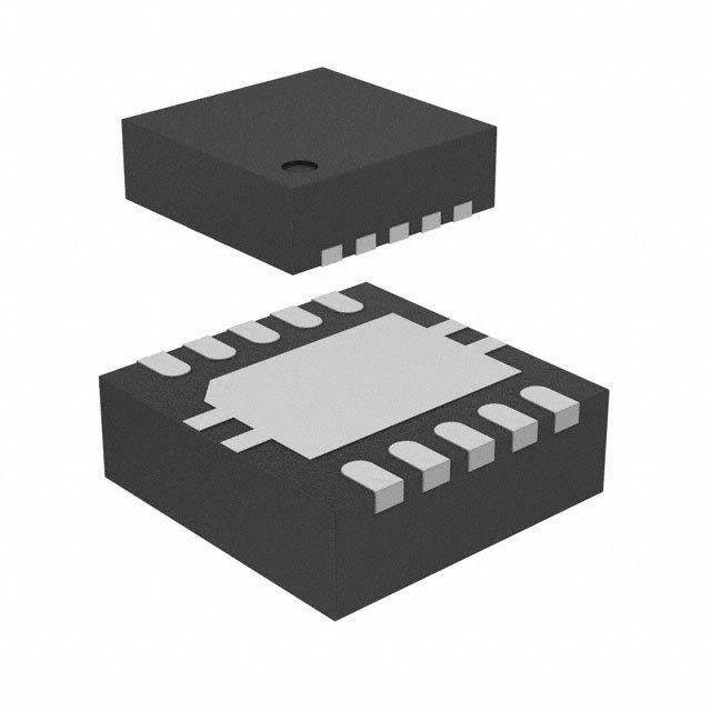
| 产品图片 |
|
| rohs | 符合RoHS无铅 / 符合限制有害物质指令(RoHS)规范要求 |
| 产品系列 | 电源管理 IC,稳压器—开关式稳压器,Texas Instruments TPS61087DRCR- |
| 数据手册 | |
| 产品型号 | TPS61087DRCR |
| PCN组件/产地 | |
| PWM类型 | 电流模式 |
| 产品目录页面 | |
| 产品种类 | 稳压器—开关式稳压器 |
| 供应商器件封装 | 10-SON(3x3) |
| 其它名称 | 296-27012-2 |
| 包装 | 带卷 (TR) |
| 单位重量 | 30 mg |
| 同步整流器 | 无 |
| 商标 | Texas Instruments |
| 安装类型 | 表面贴装 |
| 安装风格 | SMD/SMT |
| 宽度 | 3 mm |
| 封装 | Reel |
| 封装/外壳 | 10-VFDFN 裸露焊盘 |
| 封装/箱体 | VSON-10 |
| 工作温度 | -40°C ~ 85°C |
| 工作温度范围 | - 40 C to + 85 C |
| 工厂包装数量 | 3000 |
| 开关频率 | 650 kHz, 1.2 MHz |
| 拓扑结构 | Boost |
| 最大工作温度 | + 85 C |
| 最大输入电压 | 6 V |
| 最小工作温度 | - 40 C |
| 最小输入电压 | 2.5 V |
| 标准包装 | 3,000 |
| 电压-输入 | 2.5 V ~ 6 V |
| 电压-输出 | 3 V ~ 18.5 V |
| 电流-输出 | 3.2A |
| 类型 | 升压(升压) |
| 系列 | TPS61087 |
| 负载调节 | 0.11 %/A |
| 输出数 | 1 |
| 输出电压 | 18.5 V |
| 输出电流 | 3.2 A |
| 输出端数量 | 1 Output |
| 输出类型 | 可调式 |
| 配用 | /product-detail/zh/TPS61087EVM-317/296-31223-ND/2047999 |
| 频率-开关 | 650kHz,1.2MHz |


- 商务部:美国ITC正式对集成电路等产品启动337调查
- 曝三星4nm工艺存在良率问题 高通将骁龙8 Gen1或转产台积电
- 太阳诱电将投资9.5亿元在常州建新厂生产MLCC 预计2023年完工
- 英特尔发布欧洲新工厂建设计划 深化IDM 2.0 战略
- 台积电先进制程称霸业界 有大客户加持明年业绩稳了
- 达到5530亿美元!SIA预计今年全球半导体销售额将创下新高
- 英特尔拟将自动驾驶子公司Mobileye上市 估值或超500亿美元
- 三星加码芯片和SET,合并消费电子和移动部门,撤换高东真等 CEO
- 三星电子宣布重大人事变动 还合并消费电子和移动部门
- 海关总署:前11个月进口集成电路产品价值2.52万亿元 增长14.8%


PDF Datasheet 数据手册内容提取
Product Order Technical Tools & Support & Folder Now Documents Software Community TPS61087 SLVS821E–MAY2008–REVISEDMAY2019 TPS61087 650-kHz,1.2-MHz, 18.5-V Step-Up DC-DC Converter With 3.2-A Switch 1 Features 3 Description • 2.5-Vto6-VInputVoltageRange The TPS61087 is a high-frequency, high-efficiency 1 DC-DC converter with an integrated 3.2-A, 0.13-Ω • 18.5-VBoostConverterWith3.2-ASwitchCurrent power switch capable of providing an output voltage • 650-kHz,1.2-MHzSelectableSwitching up to 18.5 V. The selectable frequency of 650 kHz or Frequency 1.2 MHz allows the use of small external inductors • AdjustableSoft-Start and capacitors and provides fast transient response. The external compensation allows optimization of the • ThermalShutdown application for specific conditions. A capacitor • UndervoltageLockout connected to the soft-start pin minimizes inrush • 10-PinQFNandThinQFNPackages currentatstartup. 2 Applications DeviceInformation(1) PARTNUMBER PACKAGE BODYSIZE(NOM) • HandheldDevices VSON(10) • GPSReceivers TPS61087 3.00mm×3.00mm WSON(10) • DigitalStillCameras (1) For all available packages, see the orderable addendum at • PortableApplications theendofthedatasheet. • DSLModems • PCMCIACards • TFTLCDBiasSupply SimplifiedSchematic L 3.3mH VIN D VS SL22 2.5 V to 6 V 8 6 15 V/500 mA IN SW Cby 1mF Cin 16 V 3 7 R1 Cout 2* 10mF EN SW 200 kW 4* 10mF 16 V 25 V 9 2 FREQ FB R2 18 kW 4 1 AGND COMP Rcomp 5 10 100 kW PGND SS Ccomp TPS61087 Css 820 pF 100 nF 1 An IMPORTANT NOTICE at the end of this data sheet addresses availability, warranty, changes, use in safety-critical applications, intellectualpropertymattersandotherimportantdisclaimers.PRODUCTIONDATA.
TPS61087 SLVS821E–MAY2008–REVISEDMAY2019 www.ti.com Table of Contents 1 Features.................................................................. 1 7.4 DeviceFunctionalModes........................................10 2 Applications........................................................... 1 8 ApplicationandImplementation........................ 11 3 Description............................................................. 1 8.1 ApplicationInformation............................................11 4 RevisionHistory..................................................... 2 8.2 TypicalApplication .................................................11 8.3 SystemExamples...................................................17 5 PinConfigurationandFunctions......................... 4 9 PowerSupplyRecommendations...................... 22 6 Specifications......................................................... 4 10 Layout................................................................... 22 6.1 AbsoluteMaximumRatings......................................4 6.2 ESDRatings..............................................................5 10.1 LayoutGuidelines.................................................22 6.3 RecommendedOperatingConditions.......................5 10.2 LayoutExample....................................................23 6.4 ThermalInformation..................................................5 11 DeviceandDocumentationSupport................. 24 6.5 ElectricalCharacteristics...........................................5 11.1 Third-PartyProductsDisclaimer...........................24 6.6 TypicalCharacteristics..............................................6 11.2 Trademarks...........................................................24 7 DetailedDescription.............................................. 9 11.3 ElectrostaticDischargeCaution............................24 7.1 Overview...................................................................9 11.4 Glossary................................................................24 7.2 FunctionalBlockDiagram.........................................9 12 Mechanical,Packaging,andOrderable Information........................................................... 24 7.3 FeatureDescription.................................................10 4 Revision History NOTE:Pagenumbersforpreviousrevisionsmaydifferfrompagenumbersinthecurrentversion. ChangesfromRevisionD(August2014)toRevisionE Page • ChangeddevicenumberfromTPS61085(typo)toTPS61087(correct)intheApplicationInformationdescription paragraph. ........................................................................................................................................................................... 11 • ChangeddevicenumberfromTPS61085(typo)toTPS61087(correct)inthePowerSupplyRecommendations section.................................................................................................................................................................................. 22 ChangesfromRevisionC(July2013)toRevisionD Page • AddedESDRatingstable,FeatureDescriptionsection,DeviceFunctionalModes,ApplicationandImplementation section,PowerSupplyRecommendationssection,Layoutsection,DeviceandDocumentationSupportsection,and Mechanical,Packaging,andOrderableInformationsection.................................................................................................. 1 ChangesfromRevisionB(March2010)toRevisionC Page • AddedV TestConditionforEN,V =2.5Vto4.3V........................................................................................................... 6 IH IN ChangesfromRevisionA(June2008)toRevisionB Page • AddedDSCpackagetoPINASSIGNMENT.......................................................................................................................... 4 • DeletedLeadtemperaturefromAbsoluteMaximumRatings................................................................................................. 4 • Changedf tof inElectricalCharacteristicsBoostConverterOscillatorFrequency.......................................................... 6 osc S • ChangedFREQ=hightoFREQ=V inElectricalCharacteristicsBoostConverterOscillatorFrequency......................... 6 IN • ChangedFREQ=lowtoFREQ=GNDinElectricalCharacteristicsBoostConverterOscillatorFrequency....................... 6 • AddedMaximumloadcurrentvs.Inputvoltagegraph........................................................................................................... 6 • AddedMaximumloadcurrentvs.Inputvoltagegraph........................................................................................................... 6 • Changedftof andFrequencytoOscillatorFrequencyinFigure6 ..................................................................................... 7 S • Changedftof andFrequencytoOscillatorFrequencyinFigure7 ..................................................................................... 7 S • ChangedthetextintheDetailedDescription......................................................................................................................... 9 • Changed"inductorcurrentrippleisbelow20%"to"inductorcurrentrippleisbelow35%" ............................................... 13 2 SubmitDocumentationFeedback Copyright©2008–2019,TexasInstrumentsIncorporated ProductFolderLinks:TPS61087
TPS61087 www.ti.com SLVS821E–MAY2008–REVISEDMAY2019 • Addedoutputcapacitorcalculation....................................................................................................................................... 15 ChangesfromOriginal(May2008)toRevisionA Page • AddedtexttotheDetailedDescription-followingtheBlockDiagram................................................................................... 9 Copyright©2008–2019,TexasInstrumentsIncorporated SubmitDocumentationFeedback 3 ProductFolderLinks:TPS61087
TPS61087 SLVS821E–MAY2008–REVISEDMAY2019 www.ti.com 5 Pin Configuration and Functions DRC(VSON),DSC(WSON)Package 10Pins,3mm×3mm×1mm TopView COMP SS FB FREQ Thermal EN Pad IN AGND SW PGND SW PinFunctions PIN I/O DESCRIPTION NAME NO. AGND 4, Analogground Thermal Pad COMP 1 I/O Compensationpin EN 3 I Shutdowncontrolinput.Connectthispintologichighleveltoenablethedevice FB 2 I Feedbackpin FREQ 9 I Frequencyselectpin.Thepowerswitchoperatesat650kHzifFREQisconnectedtoGNDandat1.2MHz ifFREQisconnectedtoIN IN 8 I Inputsupplypin PGND 5 Powerground SS 10 O Soft-startcontrolpin.Connectacapacitortothispinifsoft-startneeded.Open=nosoft-start SW 6,7 I Switchpin 6 Specifications 6.1 Absolute Maximum Ratings overoperatingfree-airtemperaturerange(unlessotherwisenoted)(1) MIN MAX UNIT InputvoltagerangeIN(2) –0.3 7.0 V VoltagerangeonpinsEN,FB,SS,FREQ,COMP –0.3 7.0 V VoltageonpinSW –0.3 20 V Continuouspowerdissipation SeeThermalInformation Operatingjunctiontemperaturerange –40 150 °C Storagetemperaturerange –65 150 °C (1) StressesbeyondthoselistedunderAbsoluteMaximumRatingsmaycausepermanentdamagetothedevice.Thesearestressratings only,andfunctionaloperationofthedeviceattheseoranyotherconditionsbeyondthoseindicatedunderRecommendedOperating Conditionsisnotimplied.Exposuretoabsolute-maximum-ratedconditionsforextendedperiodsmayaffectdevicereliability (2) Allvoltagevaluesarewithrespecttonetworkgroundterminal. 4 SubmitDocumentationFeedback Copyright©2008–2019,TexasInstrumentsIncorporated ProductFolderLinks:TPS61087
TPS61087 www.ti.com SLVS821E–MAY2008–REVISEDMAY2019 6.2 ESD Ratings VALUE UNIT Humanbodymodel(HBM),perANSI/ESDA/JEDECJS-001(1) ±2000 Charged-devicemodel(CDM),perJEDECspecificationJESD22- ±500 V(ESD) Electrostaticdischarge C101(2) V Machinemodel(MM) ±200 (1) JEDECdocumentJEP155statesthat500-VHBMallowssafemanufacturingwithastandardESDcontrolprocess.Manufacturingwith lessthan500-VHBMispossiblewiththenecessaryprecautions.Pinslistedas±2000Vmayactuallyhavehigherperformance. (2) JEDECdocumentJEP157statesthat250-VCDMallowssafemanufacturingwithastandardESDcontrolprocess.Manufacturingwith lessthan250-VCDMispossiblewiththenecessaryprecautions.Pinslistedas±500Vmayactuallyhavehigherperformance. 6.3 Recommended Operating Conditions MIN NOM MAX UNIT V Inputvoltagerange 2.5 6 V IN V Boostoutputvoltagerange V +0.5 18.5 V S IN T Operatingfree-airtemperature –40 85 °C A T Operatingjunctiontemperature –40 125 °C J 6.4 Thermal Information TPS61087 THERMALMETRIC(1) DRC DSC UNIT 10PINS 10PINS R Junction-to-ambientthermalresistance 54.7 55.3 °C/W θJA R Junction-to-case(top)thermalresistance 67.2 84.8 °C/W θJC(top) R Junction-to-boardthermalresistance 29.6 29.7 °C/W θJB ψ Junction-to-topcharacterizationparameter 2.3 5.4 °C/W JT ψ Junction-to-boardcharacterizationparameter 29.8 29.8 °C/W JB R Junction-to-case(bottom)thermalresistance 15.6 10.9 °C/W θJC(bot) (1) Formoreinformationabouttraditionalandnewthermalmetrics,seetheICPackageThermalMetricsapplicationreport,SPRA953. 6.5 Electrical Characteristics V =5V,EN=V ,V =15V,T =–40°Cto85°C,typicalvaluesareatT =25°C(unlessotherwisenoted) IN IN S A A PARAMETER TESTCONDITIONS MIN TYP MAX UNIT SUPPLY V Inputvoltagerange 2.5 6 V IN I OperatingquiescentcurrentintoIN Devicenotswitching,V =1.3V 75 100 μA Q FB I ShutdowncurrentintoIN EN=GND 1 μA SDVIN V Undervoltagelockoutthreshold V falling 2.4 V UVLO IN V rising 2.5 V IN T Thermalshutdown Temperaturerising 150 °C SD T Thermalshutdownhysteresis 14 °C SDHYS Copyright©2008–2019,TexasInstrumentsIncorporated SubmitDocumentationFeedback 5 ProductFolderLinks:TPS61087
TPS61087 SLVS821E–MAY2008–REVISEDMAY2019 www.ti.com Electrical Characteristics (continued) V =5V,EN=V ,V =15V,T =–40°Cto85°C,typicalvaluesareatT =25°C(unlessotherwisenoted) IN IN S A A PARAMETER TESTCONDITIONS MIN TYP MAX UNIT LOGICSIGNALSEN,FREQ V =2.5Vto6.0V 2 IN V High-levelinputvoltage V IH ValidonlyforEN,V =2.5Vto4.3V 1.6 IN V Low-levelinputvoltage V =2.5Vto6.0V 0.5 V IL IN I Inputleakagecurrent EN=FREQ=GND 0.1 μA INLEAK BOOSTCONVERTER V + V Boostoutputvoltage IN 18.5 V S 0.5 V Feedbackregulationvoltage 1.230 1.238 1.246 V FB gm Transconductanceerroramplifier 107 μA/V I Feedbackinputbiascurrent V =1.238V 0.1 μA FB FB V =V =5V,I =currentlimit 0.13 0.18 IN GS SW r N-channelMOSFETon-resistance Ω DS(on) V =V =3V,I =currentlimit 0.16 0.23 IN GS SW I SWleakagecurrent EN=GND,V =V =6.0V 2 μA SWLEAK SW IN I N-ChannelMOSFETcurrentlimit 3.2 4.0 4.8 A LIM I Soft-startcurrent V =1.238V 7 10 13 μA SS SS FREQ=V 0.9 1.2 1.5 MHz IN f Oscillatorfrequency S FREQ=GND 480 650 820 kHz Lineregulation V =2.5Vto6.0V,I =10mA 0.0002 %/V IN OUT Loadregulation V =5.0V,I =1mAto1A 0.11 %/A IN OUT 6.6 Typical Characteristics Thetypicalcharacteristicsaremeasuredwiththeinductors74477890033.3µH(highfrequency)or744540686.8µH(low frequency)fromWurthandtherectifierdiodeSL22. Table1.TableofGraphs FIGURE I Maximumloadcurrent vs.InputvoltageatHighfrequency(1.2MHz) Figure1 OUT(max) I Maximumloadcurrent vs.InputvoltageatLowfrequency(650kHz) Figure2 OUT(max) η Efficiency vs.Loadcurrent,V =15V,V =5V Figure3 S IN η Efficiency vs.Loadcurrent,V =9V,V =3.3V Figure4 S IN Supplycurrent vs.Supplyvoltage Figure5 Oscillatorfrequency vs.Loadcurrent Figure6 Oscillatorfrequency vs.Supplyvoltage Figure7 6 SubmitDocumentationFeedback Copyright©2008–2019,TexasInstrumentsIncorporated ProductFolderLinks:TPS61087
TPS61087 www.ti.com SLVS821E–MAY2008–REVISEDMAY2019 3.0 3.0 fS= 650 kHz fS= 1.2 Mhz A 2.5 A 2.5 nt - V = 9 V nt - e OUT e urr 2.0 urr 2.0 C C V = 9 V oad VOUT= 12 V oad OUT VOUT= 12 V L 1.5 L 1.5 m V = 15 V m u OUT u m m Maxi 1.0 Maxi 1.0 I- OUT 0.5 VOUT= 18.5 V I- OUT 0.5 VOUT= 18.5 V V = 15 V OUT 0.0 0.0 2.5 3.0 3.5 4.0 4.5 5.0 5.5 6.0 2.5 3.0 3.5 4.0 4.5 5.0 5.5 6.0 VIN- Input Voltage - V VIN- Input Voltage - V Figure1.MaximumLoadCurrentvsInputVoltage Figure2.MaximumLoadCurrentvsInputVoltage 100 100 fS= 650 kHz 90 90 L= 6.8mH 80 fS= 1.2 Mhz 80 70 L= 3.3mH fS= 650 kHz 70 fS= 1.2 Mhz L= 6.8mH L= 3.3mH % 60 % 60 ncy - 50 ncy - 50 cie cie Effi 40 Effi 40 30 30 20 20 VIN= 5 V VIN= 3.3 V 10 VS= 15 V 10 VS= 9 V 0 0 0.0 0.1 0.2 0.3 0.4 0.5 0.6 0.7 0.8 0.9 1.0 1.1 0.0 0.1 0.2 0.3 0.4 0.5 0.6 0.7 0.8 0.9 1.0 1.1 IOUT- Load Current -A IOUT- Load Current -A Figure3.EfficiencyvsLoadCurrent Figure4.EfficiencyvsLoadCurrent 2.0 1600 1.8 SWITCHING fS= 1.2 Mhz 1400 FREQ = VIN 1.6 L= 3.3mH Hz L= 3.3mH ent - mA 11..24 SfSW=I T6C50H IkNHGz uency - k11020000 Supply Curr 01..80 L= 6.8mH cillator Freq 680000 FLR=E 6Q.8 =m GHND I- CC 0.6 - OsS 400 0.4 f 0.2 NOT SWITCHING 200 VVISN== 1 55 VV 0 0 2.5 3.0 3.5 4.0 4.5 5.0 5.5 6.0 0.0 0.1 0.2 0.3 0.4 0.5 0.6 0.7 0.8 0.9 1.0 VCC- Supply Voltage - V IOUT- Load Current - mA Figure6.OscillatorFrequencyvsLoadCurrent Figure5.SupplyCurrentvsSupplyVoltage Copyright©2008–2019,TexasInstrumentsIncorporated SubmitDocumentationFeedback 7 ProductFolderLinks:TPS61087
TPS61087 SLVS821E–MAY2008–REVISEDMAY2019 www.ti.com 1400 VS= 15 V / 200 mA 1200 Hz FREQ = VIN y - k 1000 L= 3.3mH c n e u 800 q e Fr scillator 600 FLR=E 6Q.8 =m GHND O 400 - S f 200 0 2.5 3 3.5 4 4.5 5 5.5 6 VCC- Supply Voltage - V Figure7.OscillatorFrequencyvsSupplyVoltage 8 SubmitDocumentationFeedback Copyright©2008–2019,TexasInstrumentsIncorporated ProductFolderLinks:TPS61087
TPS61087 www.ti.com SLVS821E–MAY2008–REVISEDMAY2019 7 Detailed Description 7.1 Overview The boost converter is designed for output voltages of up to 18.5 V with a switch peak current limit of 3.2 A minimum. The device, which operates in a current mode scheme with quasi-constant frequency, is externally compensated for maximum flexibility and stability. The switching frequency is selectable between 650 kHz and 1.2 MHz, and the minimum input voltage is 2.5 V. To limit the inrush current at start-up, a soft-start pin is available. The novel topology of the TPS60187 boost converter uses adaptive off-time to provide superior load and line transientresponses.Thistopologyalsooperatesoverawiderrangeofapplicationsthanconventionalconverters. The selectable switching frequency offers the possibility to optimize the design either for the use of small-sized components (1.2 MHz) or for higher system efficiency (650 kHz). However, the frequency changes slightly because the voltage drop across the r has some influence on the current and voltage measurement and DS(on) thusontheon-time(theoff-timeremainsconstant). The converter operates in continuous conduction mode (CCM) as soon as the input current increases above half theripplecurrentintheinductor,for lower load currents it switches into discontinuous conduction mode (DCM). If theloadisfurtherreduced,thepartstartstoskippulsestomaintaintheoutputvoltage. 7.2 Functional Block Diagram VIN VS EN IN FREQ SW SW SS Current limit and Soft Start t Generator OFF AGND Bias Vref=1.238V UVLO Thermal Shutdown t ON Gate Driver of PWM Power Generator Transistor COMP GMAmplifier FB Vref PGND Copyright©2008–2019,TexasInstrumentsIncorporated SubmitDocumentationFeedback 9 ProductFolderLinks:TPS61087
TPS61087 SLVS821E–MAY2008–REVISEDMAY2019 www.ti.com 7.3 Feature Description 7.3.1 Soft-Start The boost converter has an adjustable soft-start to prevent high inrush current during start-up. To minimize the inrush current during start-up an external capacitor, connected to the soft-start pin SS and charged with a constant current, is used to slowly ramp up the internal current limit of the boost converter. When the EN pin is pulled high, the soft-start capacitor C is immediately charged to 0.3 V. The capacitor is then charged at a SS constant current of 10 μA typically until the output of the boost converter V has reached its Power Good S threshold (roughly 98% of V nominal value). During this time, the SS voltage directly controls the peak inductor S current, starting with 0 A at V = 0.3 V up to the full current limit at V = 800 mV. The maximum load current is SS SS availableafterthesoft-startiscompleted.Thelargerthecapacitortheslowertherampofthecurrentlimitand the longer the soft-start time. A 100-nF capacitor is usually sufficient for most of the applications. When the EN pin is pulledlow,thesoft-startcapacitorisdischargedtoground. 7.3.2 FrequencySelectPin(FREQ) The frequency select pin FREQ allows to set the switching frequency of the device to 650 kHz (FREQ = low) or 1.2 MHz (FREQ = high). Higher switching frequency improves load transient response but reduces slightly the efficiency. The other benefits of higher switching frequency are a lower output ripple voltage. The use of a 1.2- MHzswitchingfrequencyisrecommendedunlesslightloadefficiencyisamajorconcern. 7.3.3 UndervoltageLockout(UVLO) To avoid mis-operation of the device at low input voltages an undervoltage lockout is included that disables the device,iftheinputvoltagefallsbelow2.4V. 7.3.4 ThermalShutdown A thermal shutdown is implemented to prevent damages due to excessive heat and power dissipation. Typically the thermal shutdown happens at a junction temperature of 150°C. When the thermal shutdown is triggered the device stops switching until the junction temperature falls below typically 136°C. Then the device starts switching again. 7.3.5 OvervoltagePrevention If overvoltage is detected on the FB pin (typically 3% above the nominal value of 1.238 V) the part stops switching immediately until the voltage on this pin drops to its nominal value. This prevents overvoltage on the outputandsecuresthecircuitsconnectedtotheoutputfromexcessiveovervoltage. 7.4 Device Functional Modes The converter operates in continuous conduction mode (CCM) as soon as the input current increases above half theripplecurrentintheinductor,for lower load currents it switches into discontinuous conduction mode (DCM). If theloadisfurtherreduced,thepartstartstoskippulsestomaintaintheoutputvoltage. 10 SubmitDocumentationFeedback Copyright©2008–2019,TexasInstrumentsIncorporated ProductFolderLinks:TPS61087
TPS61087 www.ti.com SLVS821E–MAY2008–REVISEDMAY2019 8 Application and Implementation NOTE Information in the following applications sections is not part of the TI component specification, and TI does not warrant its accuracy or completeness. TI’s customers are responsible for determining suitability of components for their purposes. Customers should validateandtesttheirdesignimplementationtoconfirmsystemfunctionality. 8.1 Application Information The TPS61087 is designed for output voltages up to 18.5 V with a switch peak current limit of 2.0-A minimum. The device, which operates in a current mode scheme with quasi-constant frequency, is externally compensated for maximum flexibility and stability. The switching frequency is selectable between 650 kHz and 1.2 MHz, and the input voltage range is 2.3 V to 6.0 V. To control the inrush current at start-up a soft-start pin is available. The following section provides a step-by-step design approach for configuring the TPS61087 as a voltage regulating boostconverter. 8.2 Typical Application L 3.3 µH VIN D VS 5 V ± 20% 8 6 SL22 15 V/900 mAmax. IN SW Cby 1 µF Cin 16 V 3 7 R1 Cout 2* 10 µF EN SW 200 kΩ 4* 10 µF 16 V 25 V 9 2 FREQ FB R2 18 kΩ 4 1 AGND COMP Rcomp 5 10 100 kΩ PGND SS Ccomp TPS61087 Css 820 pF 100 nF Figure8. TypicalApplication,5Vto15V(f =1.2MHz) S 8.2.1 DesignRequirements Table2.TPS6108715-VOutputDesignRequirements PARAMETERS VALUES InputVoltage 5V±20% OutputVoltage 15V OutputCurrent 900mA SwitchingFrequency 1.2MHz Copyright©2008–2019,TexasInstrumentsIncorporated SubmitDocumentationFeedback 11 ProductFolderLinks:TPS61087
TPS61087 SLVS821E–MAY2008–REVISEDMAY2019 www.ti.com 8.2.2 DetailedDesignProcedure Thefirststepinthedesignprocedureis to verify that the maximum possible output current of the boost converter supports the specific application requirements. A simple approach is to estimate the converter efficiency, by taking the efficiency numbers from the provided efficiency curves or to use a worst case assumption for the expectedefficiency,forexample,90%. 1.Dutycycle,D: V ×h D=1- IN V S (1) 2.Maximumoutputcurrent,I : out(max) Iout(max) =æçèILIM(min)-D2IL ö÷ø×(1-D) (2) 3.Peakswitchcurrentinapplication,I : swpeak DI I I = L + out swpeak 2 1-D (3) withtheinductorpeak-to-peakripplecurrent,ΔI L V ×D DI = IN L f ×L S (4) and V Minimuminputvoltage IN V Outputvoltage S I Converterswitchcurrentlimit(minimumswitchcurrentlimit=3.2A) LIM(min) f Converterswitchingfrequency(typically1.2MHzor650kHz) S L Selectedinductorvalue η Estimatedconverterefficiency(usethenumberfromtheefficiencyplotsor90%asanestimation) The peak switch current is the steady state peak switch current that the integrated switch, inductor and external Schottky diode has to be able to handle. The calculation must be done for the minimum input voltage where the peakswitchcurrentisthehighest. 8.2.2.1 InductorSelection The TPS61087 is designed to work with a wide range of inductors. The main parameter for the inductor selection is the saturation current of the inductor which should be higher than the peak switch current as calculated in the Detailed Design Procedure section with additional margin to cover for heavy load transients. An alternative, more conservative, is to choose an inductor with a saturation current at least as high as the maximum switch current limit of 4.8 A. The other important parameter is the inductor DC resistance. Usually the lower the DC resistance the higher the efficiency. It is important to note that the inductor DC resistance is not the only parameter determining the efficiency. Especially for a boost converter where the inductor is the energy storage element, the type and core material of the inductor influences the efficiency as well. At high switching frequencies of 1.2 MHz inductor core losses, proximity effects and skin effects become more important. Usually an inductor with a larger form factor gives higher efficiency. The efficiency difference between different inductors can vary between 2% to 10%. For the TPS61087, inductor values between 3 μH and 6 μH are a good choice with a switching frequency of 1.2 MHz, typically 3.3 μH. At 650 kHz TI recommends inductors between 6 μH and 13 μH, typically 6.8 μH. PossibleinductorsareshowninTable3. 12 SubmitDocumentationFeedback Copyright©2008–2019,TexasInstrumentsIncorporated ProductFolderLinks:TPS61087
TPS61087 www.ti.com SLVS821E–MAY2008–REVISEDMAY2019 Typically, TI recommends an inductor current ripple below 35% of the average inductor current. Therefore, the followingequationcanbeusedtocalculatetheinductorvalue, L: 2 æV ö æV -V ö æ h ö L = çèVISN ÷ø ×çèIoSut× fINS ÷ø×çè0.35÷ø (5) with V Minimuminputvoltage IN V Outputvoltage S I Maximumoutputcurrentintheapplication out f Converterswitchingfrequency(typically1.2MHzor650kHz) S η Estimatedconverterefficiency(usethenumberfromtheefficiencyplotsor90%asanestimation) Table3.InductorSelection L COMPONENT SIZE DCRTYP SUPPLIER I (A) (μH) CODE (L×W×Hmm) (mΩ) sat 1.2MHz 4.2 Sumida CDRH5D28 5.7×5.7×3 23 2.2 4.7 WurthElektronik 7447785004 5.9×6.2×3.3 60 2.5 5 Coilcraft MSS7341 7.3×7.3×4.1 24 2.9 5 Sumida CDRH6D28 7×7×3 23 2.4 4.6 Sumida CDR7D28 7.6×7.6×3 38 3.15 4.7 WurthElektronik 7447789004 7.3×7.3×3.2 33 3.9 3.3 WurthElektronik 7447789003 7.3×7.3×3.2 30 4.2 650kHz 10 WurthElektronik 744778910 7.3×7.3×3.2 51 2.2 10 Sumida CDRH8D28 8.3×8.3×3 36 2.7 6.8 Sumida CDRH6D26HPNP 7×7×2.8 52 2.9 6.2 Sumida CDRH8D58 8.3×8.3×6 25 3.3 10 Coilcraft DS3316P 12.95×9.40× 80 3.5 5.08 10 Sumida CDRH8D43 8.3×8.3×4.5 29 4 6.8 WurthElektronik 74454068 12.7×10×4.9 55 4.1 8.2.2.2 RectifierDiodeSelection To achieve high efficiency a Schottky type should be used for the rectifier diode. The reverse voltage rating should be higher than the maximum output voltage of the converter. The averaged rectified forward current I , avg theSchottkydiodeneedstoberatedfor,isequaltotheoutputcurrent I : out I = I avg out (6) Usually a Schottky diode with 2-A maximum average rectified forward current rating is sufficient for most applications. The Schottky rectifier can be selected with lower forward current capability depending on the output current I but has to be able to dissipate the power. The dissipated power, P , is the average rectified forward out D currenttimesthediodeforwardvoltage, V . forward P =I ×V D avg forward (7) Typically, the diode should be able to dissipate around 500 mW depending on the load current and forward voltage. Copyright©2008–2019,TexasInstrumentsIncorporated SubmitDocumentationFeedback 13 ProductFolderLinks:TPS61087
TPS61087 SLVS821E–MAY2008–REVISEDMAY2019 www.ti.com Table4.RectifierDiodeSelection CURRENT V V /I SUPPLIER COMPONENTCODE RATINGI r forward avg avg 2A 20V 0.44V/2A VishaySemiconductor SL22 2A 20V 0.5V/2A FairchildSemiconductor SS22 8.2.2.3 SettingtheOutputVoltage The output voltage is set by an external resistor divider. Typically, a minimum current of 50 μA flowing through the feedback divider gives good accuracy and noise covering. A standard low-side resistor of 18 kΩ is typically selected.Theresistorsarethencalculatedas: V S V æ V ö R2= FB »18kW R1=R2×ç S -1÷ 70mA èVFB ø R1 V FB V =1.238V R2 FB (8) 8.2.2.4 Compensation(COMP) The regulator loop can be compensated by adjusting the external components connected to the COMP pin. The COMPpinistheoutputoftheinternaltransconductanceerroramplifier. Standardvaluesof R =16kΩ andC =2.7nF willworkforthemajorityoftheapplications. COMP COMP See Table 5 for dedicated compensation networks giving an improved load transient response. The following equationscanbeusedtocalculateR andC : COMP COMP R = 110×VIN ×VS ×Cout C = Vs×Cout COMP L×I COMP 7.5×I ×R out out COMP (9) with V Minimuminputvoltage IN V Outputvoltage S C Outputcapacitance out L Inductorvalue,forexample,3.3μHor6.8μH I Maximumoutputcurrentintheapplication out MakesurethatR <120kΩ andC >820pF,independentoftheresultsoftheaboveformulas. COMP COMP Table5.RecommendedCompensationNetworkValuesatHigh/LowFrequency FREQUENCY L V V ±20% R C S IN COMP COMP 5V 100kΩ 820pF 15V 3.3V 91kΩ 1.2nF 5V 68kΩ 820pF High(1.2MHz) 3.3μH 12V 3.3V 68kΩ 1.2nF 5V 39kΩ 820pF 9V 3.3V 39kΩ 1.2nF 5V 51kΩ 1.5nF 15V 3.3V 47kΩ 2.7nF 5V 33kΩ 1.5nF Low(650kHz) 6.8μH 12V 3.3V 33kΩ 2.7nF 5V 18kΩ 1.5nF 9V 3.3V 18kΩ 2.7nF 14 SubmitDocumentationFeedback Copyright©2008–2019,TexasInstrumentsIncorporated ProductFolderLinks:TPS61087
TPS61087 www.ti.com SLVS821E–MAY2008–REVISEDMAY2019 Table 5 gives conservative R and C values for certain inductors, input and output voltages providing a COMP COMP very stable system. For a faster response time, a higher R value can be used to enlarge the bandwidth, as COMP well as a slightly lower value of C to keep enough phase margin. These adjustments should be performed in COMP parallelwiththeloadtransientresponsemonitoringofTPS61087. 8.2.2.5 InputCapacitorSelection For good input voltage filtering low ESR ceramic capacitors are recommended. TPS61087 has an analog input IN.Therefore,a1-μFbypassishighlyrecommendedascloseaspossibletotheICfromINtoGND. Two 10-μF (or one 22-μF) ceramic input capacitors are sufficient for most of the applications. For better input voltage filtering this value can be increased. See Table 6 and typical applications for input capacitor recommendation. 8.2.2.6 OutputCapacitorSelection For best output voltage filtering a low ESR output capacitor like ceramic capcaitor is recommended. Four 10-μF ceramic output capacitors (or two-22 μF) work for most of the applications. Higher capacitor values can be used toimprovetheloadtransientresponse.SeeTable6fortheselectionoftheoutputcapacitor. Table6.RectifierInputandOutputCapacitorSelection CAPACITOR/SIZE VOLTAGERATING SUPPLIER COMPONENTCODE C 22μF/1206 16V TaiyoYuden EMK316BJ226ML IN INbypass 1μF/0603 16V TaiyoYuden EMK107BJ105KA C 10μF/1206 25V TaiyoYuden TMK316BJ106KL OUT Tocalculatetheoutputvoltageripple,thefollowingequationcanbeused: V -V I DV = S IN × out DV =I ×R C V × f C C_ESR L(peak) C_ESR S S out (10) with ΔV Outputvoltagerippledependentonoutputcapacitance,outputcurrentandswitchingfrequency C V Outputvoltage S V Minimuminputvoltageofboostconverter IN f Converterswitchingfrequency(typically1.2MHzor650kHz) S I Outputcapacitance out ΔV OutputvoltagerippleduetooutputcapacitorsESR(equivalentseriesresistance) C_ESR I Inductorpeakswitchcurrentintheapplication SWPEAK R Outputcapacitorsequivalentseriesresistance(ESR) C_ESR ΔV canbeneglectedinmanycasessinceceramiccapacitorsprovidelowESR. C_ESR Copyright©2008–2019,TexasInstrumentsIncorporated SubmitDocumentationFeedback 15 ProductFolderLinks:TPS61087
TPS61087 SLVS821E–MAY2008–REVISEDMAY2019 www.ti.com 8.2.3 ApplicationCurves VSW VSW 10 V/div 10 V/div VS_AC VS_AC 50 mV/div 50 mV/div VIN= 5 V VS= 15 V/2 mA Il FREQ = VIN 1A/div VIN= 5 V IL VS= 15 V/500 mA 500 mA/div FREQ = VIN 200 ns/div 200 ns/div Figure9.PWMSwitchingDiscontinuousConductionMode Figure10.PWMSwitchingContinuousConductionMode VVISN== 1 55 VV VVISN== 1 55 VV CLO=U 6T.8= m4H0mF VS_AC Rcomp= 110 kW 100 mV/div Ccomp= 1 nF COUT= 40mF VS_AC L= 3.3mH 100 mV/div Rcomp= 150 kW IOUT= 100 mA- 500 mA Ccomp= 820 pF IOUT= 100 mA- 500 mA IOUT 200 mA/div IOUT 200 mA/div 200ms/div 200ms/div Figure11.LoadTransientResponseHighFrequency Figure12.LoadTransientResponseLowFrequency (1.2MHz) (650kHz) EN 5 V/div V = 5 V IN V = 15 V/500 mA S V S 5 V/div C = 100 nF SS I L 1A/div 2 ms/div Figure13.Soft-Start 16 SubmitDocumentationFeedback Copyright©2008–2019,TexasInstrumentsIncorporated ProductFolderLinks:TPS61087
TPS61087 www.ti.com SLVS821E–MAY2008–REVISEDMAY2019 8.3 System Examples 8.3.1 GeneralBoostApplicationCircuits L 6.8 µH V D V IN S 5 V ± 20% SL22 15 V/900 mAmax. 8 6 IN SW Cby 1 µF Cin 16 V 3 7 R1 Cout 2* 10 µF EN SW 200 kΩ 4* 10 µF 16 V 25 V 9 2 FREQ FB R2 18 kΩ 4 1 AGND COMP Rcomp 5 10 51 kΩ PGND SS Ccomp TPS61087 Css 1.5 nF 100 nF Figure14. TypicalApplication,5Vto15V(f =650kHz) S L 3.3 µH VIN D VS SL22 3.3 V ± 20% 8 6 9 V/950 mAmax. IN SW Cby 1 µF Cin 16 V 3 7 R1 Cout 2* 10 µF EN SW 110 kΩ 4* 10 µF 16 V 25 V 9 2 FREQ FB R2 18 kΩ 4 1 AGND COMP Rcomp 5 10 39 kΩ PGND SS Ccomp TPS61087 Css 1.2 nF 100 nF Figure15. TypicalApplication,3.3Vto9V(f =1.2MHz) S Copyright©2008–2019,TexasInstrumentsIncorporated SubmitDocumentationFeedback 17 ProductFolderLinks:TPS61087
TPS61087 SLVS821E–MAY2008–REVISEDMAY2019 www.ti.com System Examples (continued) L 6.8 µH VIN D VS 3.3 V ± 20% 8 6 SL22 9 V/950 mAmax. IN SW Cby 1 µF Cin 16 V 3 7 R1 Cout 2* 10 µF EN SW 110 kΩ 4* 10 µF 16 V 25 V 9 2 FREQ FB R2 18 kΩ 4 1 AGND COMP Rcomp 5 10 18 kΩ PGND SS Ccomp TPS61087 Css 2.7 nF 100 nF Figure16. TypicalApplication,3.3Vto9V(f =650kHz) S Riso 10 kW L 6.8 µH VIN 1 µCFb/1y6 V SLD22 BC857C VS 5 V ± 20% 8 6 15 V/300 mA IN SW Ciso 2* 10 CµFin/ 3 EN SW 7 1 µF/ 25 V R1 Cout 16 V 200 kΩ 4*10 µF/ 25 V 9 2 FREQ FB R2 4 1 18 kΩ Enable AGND COMP Rcomp 5 10 PGND SS 51 kΩ Ccomp TPS61087 Css 1.5 nF 100 nF Figure17. TypicalApplicationWithExternalLoadDisconnectSwitch 18 SubmitDocumentationFeedback Copyright©2008–2019,TexasInstrumentsIncorporated ProductFolderLinks:TPS61087
TPS61087 www.ti.com SLVS821E–MAY2008–REVISEDMAY2019 System Examples (continued) L 6.8 µH Overvoltage V D V IN Protection S SL22 5 V ± 20% 15 V/900 mAmax. 8 6 IN SW Cby Dz 1 µF BZX84C 18V Cin 16 V 3 7 R1 Cout 2* 10 µF EN SW 200 kΩ 4* 10 µF 16 V 25 V 9 2 FREQ FB Rlimit R2 110Ω 4 1 18 kΩ AGND COMP Rcomp 5 10 51 kΩ PGND SS Ccomp TPS61087 Css 1.5 nF 100 nF Figure18. TypicalApplication,5Vto15V(f =1.2MHz)WithOvervoltageProtection S Copyright©2008–2019,TexasInstrumentsIncorporated SubmitDocumentationFeedback 19 ProductFolderLinks:TPS61087
TPS61087 SLVS821E–MAY2008–REVISEDMAY2019 www.ti.com System Examples (continued) 8.3.2 TFTLCDApplication T2 Vgh 3·Vs BC850B 26.5 V/20 mA C16 -7 V/V2G0L mA BCT8157B -Vs 47500 nVF/ BAVD939 470C n1F8/ R10 50 V 13 kΩ R8 D4 C15 1C µ1F3/ 6.8 kΩ C14 BAV99 45700 V nF/ C17 2·Vs C20 35 V 470 nF/ 470 nF/ 1 µF/ 25 V 50 V D2 C19 35 V BAV99 470 nF/ D9 D8 50 V BZX84C27V BZX84C7V5 L 3.3 µH Cby D VIN 11 6µ FV/ SL22 VS 5 V ± 20% 8 6 15 V/500 mA IN SW Cin 3 7 R1 Cout 2*10 µF/ EN SW 200 kΩ 4*10µF/ 16 V 25V 9 2 FREQ FB R2 18 kΩ 4 1 AGND COMP Rcomp 5 10 100 kΩ PGND SS Ccomp TPS61087 820 pF Css 100 nF Figure19. TypicalApplication5Vto15V(f =1.2MHz)forTFTLCDWithExternalChargePumps S (VGH,VGL) 20 SubmitDocumentationFeedback Copyright©2008–2019,TexasInstrumentsIncorporated ProductFolderLinks:TPS61087
TPS61087 www.ti.com SLVS821E–MAY2008–REVISEDMAY2019 System Examples (continued) 8.3.3 WhiteLEDApplications L 6.8 µH optional Cby 5 V V±I N20% 1 µF/ 16 V8 6 SDL22 BZX8D4Cz 18 V 3SLW3P Ew6L7ECD 500V SmA IN SW Cin 3 7 Cout 2* 10 µF/ EN SW 4* 10 µF/ 16 V 25 V 9 2 FREQ FB Rlimit 4 1 110Ω Rsense AGND COMP 15Ω Rcomp 5 10 51 kΩ PGND SS Ccomp TPS61087 Css 1.5 nF 100 nF Figure20. SimpleApplication(5VInputVoltage)(f =650kHz)forwLEDSupply(3S3P)(WithOptional S ClampingZenerDiode) L 6.8 µH optional Cby 5 V V±I N20% 1 µF/ 16 V8 6 SDL22 BZX8D4Cz 18 V 3SLW3P Ew6L7ECD 500V SmA IN SW Cin 3 7 Cout 2* 10 µF/ EN SW 4* 10 µF/ 16 V 25 V 9 2 FREQ FB Rlimit 4 1 110Ω Rsense AGND COMP 15Ω PWM Rcomp 100 Hz to 500 Hz 5 PGND SS 10 51 kΩ Ccomp TPS61087 Css 1.5 nF 100 nF Figure21. SimpleApplication(5VInputVoltage)(f =650kHz)forwLEDSupply(3S3P)WithAdjustable S BrightnessControlUsingaPWMSignalontheEnablePin (WithOptionalClampingZenerDiode) Copyright©2008–2019,TexasInstrumentsIncorporated SubmitDocumentationFeedback 21 ProductFolderLinks:TPS61087
TPS61087 SLVS821E–MAY2008–REVISEDMAY2019 www.ti.com System Examples (continued) L 6.8 µH optional Cby 5 V V±I N20% 1 µF/ 16 V8 6 SDL22 BZX8D4Cz 18 V 3SLW3P Ew6L7ECD 500V SmA IN SW Cin 3 7 Cout 2* 10 µF/ EN SW 4* 10 µF/ 16 V 25 V 9 2 R1 Rlimit FREQ FB 180 kΩ 110Ω 4 1 Rsense AGND COMP 15Ω Rcomp R2 5 PGND SS 10 51 kΩ 127 kΩ Ccomp TPS61087 1.5 nF Analog Brightness Control Css 3.3 V ~ wLED off 100 nF 0 V ~ l = 30 mA(each string) LED PWM Signal Can be used swinging from 0 V to 3.3 V Figure22. SimpleApplication(5VInputVoltage)(f =650kHz)forwLEDSupply(3S3P)WithAdjustable S BrightnessControlUsinganAnalogSignalontheFeedbackPin (WithOptionalClampingZenerDiode) 9 Power Supply Recommendations The TPS61087 is designed to operate from an input voltage supply range from 2.3 V to 6.0 V. The power supply to the TPS61087 must have a current rating according to the supply voltage, output voltage, and output current oftheTPS61087. 10 Layout 10.1 Layout Guidelines For all switching power supplies, the layout is an important step in the design, especially at high peak currents and high switching frequencies. If the layout is not carefully done, the regulator could show stability problems as well as EMI problems. Therefore, use wide and short traces for the main current path and for the power ground tracks. The input capacitor, output capacitor, and the inductor should be placed as close as possible to the IC. Use a common ground node for power ground and a different one for control ground to minimize the effects of ground noise. Connect these ground nodes at the GND terminal of the IC. The most critical current path for all boost converters is from the switching FET, through the rectifier diode, then the output capacitors, and back to ground of the switching FET. Therefore, the output capacitors and their traces should be placed on the same boardlayerastheICandascloseaspossiblebetweentheSWpinandtheGNDterminaloftheIC.. 22 SubmitDocumentationFeedback Copyright©2008–2019,TexasInstrumentsIncorporated ProductFolderLinks:TPS61087
TPS61087 www.ti.com SLVS821E–MAY2008–REVISEDMAY2019 10.2 Layout Example VIN VOUT Q E SS FR IN SW SW 0 9 8 7 65 1 TPS61087 GND 1 2 3 4 5 D P B ND N M F EN G O G P C A Figure23. TPS61087LayoutExample Copyright©2008–2019,TexasInstrumentsIncorporated SubmitDocumentationFeedback 23 ProductFolderLinks:TPS61087
TPS61087 SLVS821E–MAY2008–REVISEDMAY2019 www.ti.com 11 Device and Documentation Support 11.1 Third-Party Products Disclaimer TI'S PUBLICATION OF INFORMATION REGARDING THIRD-PARTY PRODUCTS OR SERVICES DOES NOT CONSTITUTE AN ENDORSEMENT REGARDING THE SUITABILITY OF SUCH PRODUCTS OR SERVICES OR A WARRANTY, REPRESENTATION OR ENDORSEMENT OF SUCH PRODUCTS OR SERVICES, EITHER ALONEORINCOMBINATIONWITHANYTIPRODUCTORSERVICE. 11.2 Trademarks Alltrademarksarethepropertyoftheirrespectiveowners. 11.3 Electrostatic Discharge Caution Thesedeviceshavelimitedbuilt-inESDprotection.Theleadsshouldbeshortedtogetherorthedeviceplacedinconductivefoam duringstorageorhandlingtopreventelectrostaticdamagetotheMOSgates. 11.4 Glossary SLYZ022—TIGlossary. Thisglossarylistsandexplainsterms,acronyms,anddefinitions. 12 Mechanical, Packaging, and Orderable Information The following pages include mechanical, packaging, and orderable information. This information is the most current data available for the designated devices. This data is subject to change without notice and revision of thisdocument.Forbrowser-basedversionsofthisdatasheet,refertotheleft-handnavigation. 24 SubmitDocumentationFeedback Copyright©2008–2019,TexasInstrumentsIncorporated ProductFolderLinks:TPS61087
PACKAGE OPTION ADDENDUM www.ti.com 6-Feb-2020 PACKAGING INFORMATION Orderable Device Status Package Type Package Pins Package Eco Plan Lead/Ball Finish MSL Peak Temp Op Temp (°C) Device Marking Samples (1) Drawing Qty (2) (6) (3) (4/5) TPS61087DRCR ACTIVE VSON DRC 10 3000 Green (RoHS NIPDAU Level-2-260C-1 YEAR -40 to 85 PMOQ & no Sb/Br) TPS61087DRCRG4 ACTIVE VSON DRC 10 3000 Green (RoHS NIPDAU Level-2-260C-1 YEAR -40 to 85 PMOQ & no Sb/Br) TPS61087DRCT ACTIVE VSON DRC 10 250 Green (RoHS NIPDAU Level-2-260C-1 YEAR -40 to 85 PMOQ & no Sb/Br) TPS61087DSCR ACTIVE WSON DSC 10 3000 Green (RoHS NIPDAU Level-2-260C-1 YEAR -40 to 85 PMWI & no Sb/Br) TPS61087DSCT ACTIVE WSON DSC 10 250 Green (RoHS NIPDAU Level-2-260C-1 YEAR -40 to 85 PMWI & no Sb/Br) (1) The marketing status values are defined as follows: ACTIVE: Product device recommended for new designs. LIFEBUY: TI has announced that the device will be discontinued, and a lifetime-buy period is in effect. NRND: Not recommended for new designs. Device is in production to support existing customers, but TI does not recommend using this part in a new design. PREVIEW: Device has been announced but is not in production. Samples may or may not be available. OBSOLETE: TI has discontinued the production of the device. (2) RoHS: TI defines "RoHS" to mean semiconductor products that are compliant with the current EU RoHS requirements for all 10 RoHS substances, including the requirement that RoHS substance do not exceed 0.1% by weight in homogeneous materials. Where designed to be soldered at high temperatures, "RoHS" products are suitable for use in specified lead-free processes. TI may reference these types of products as "Pb-Free". RoHS Exempt: TI defines "RoHS Exempt" to mean products that contain lead but are compliant with EU RoHS pursuant to a specific EU RoHS exemption. Green: TI defines "Green" to mean the content of Chlorine (Cl) and Bromine (Br) based flame retardants meet JS709B low halogen requirements of <=1000ppm threshold. Antimony trioxide based flame retardants must also meet the <=1000ppm threshold requirement. (3) MSL, Peak Temp. - The Moisture Sensitivity Level rating according to the JEDEC industry standard classifications, and peak solder temperature. (4) There may be additional marking, which relates to the logo, the lot trace code information, or the environmental category on the device. (5) Multiple Device Markings will be inside parentheses. Only one Device Marking contained in parentheses and separated by a "~" will appear on a device. If a line is indented then it is a continuation of the previous line and the two combined represent the entire Device Marking for that device. (6) Lead/Ball Finish - Orderable Devices may have multiple material finish options. Finish options are separated by a vertical ruled line. Lead/Ball Finish values may wrap to two lines if the finish value exceeds the maximum column width. Addendum-Page 1
PACKAGE OPTION ADDENDUM www.ti.com 6-Feb-2020 Important Information and Disclaimer:The information provided on this page represents TI's knowledge and belief as of the date that it is provided. TI bases its knowledge and belief on information provided by third parties, and makes no representation or warranty as to the accuracy of such information. Efforts are underway to better integrate information from third parties. TI has taken and continues to take reasonable steps to provide representative and accurate information but may not have conducted destructive testing or chemical analysis on incoming materials and chemicals. TI and TI suppliers consider certain information to be proprietary, and thus CAS numbers and other limited information may not be available for release. In no event shall TI's liability arising out of such information exceed the total purchase price of the TI part(s) at issue in this document sold by TI to Customer on an annual basis. OTHER QUALIFIED VERSIONS OF TPS61087 : •Automotive: TPS61087-Q1 NOTE: Qualified Version Definitions: •Automotive - Q100 devices qualified for high-reliability automotive applications targeting zero defects Addendum-Page 2
PACKAGE MATERIALS INFORMATION www.ti.com 24-May-2019 TAPE AND REEL INFORMATION *Alldimensionsarenominal Device Package Package Pins SPQ Reel Reel A0 B0 K0 P1 W Pin1 Type Drawing Diameter Width (mm) (mm) (mm) (mm) (mm) Quadrant (mm) W1(mm) TPS61087DRCR VSON DRC 10 3000 330.0 12.4 3.3 3.3 1.1 8.0 12.0 Q2 TPS61087DRCR VSON DRC 10 3000 330.0 12.4 3.3 3.3 1.1 8.0 12.0 Q2 TPS61087DRCT VSON DRC 10 250 180.0 12.4 3.3 3.3 1.1 8.0 12.0 Q2 TPS61087DRCT VSON DRC 10 250 180.0 12.5 3.3 3.3 1.1 8.0 12.0 Q2 TPS61087DSCR WSON DSC 10 3000 330.0 12.4 3.3 3.3 1.1 8.0 12.0 Q2 TPS61087DSCT WSON DSC 10 250 180.0 12.4 3.3 3.3 1.1 8.0 12.0 Q2 PackMaterials-Page1
PACKAGE MATERIALS INFORMATION www.ti.com 24-May-2019 *Alldimensionsarenominal Device PackageType PackageDrawing Pins SPQ Length(mm) Width(mm) Height(mm) TPS61087DRCR VSON DRC 10 3000 367.0 367.0 35.0 TPS61087DRCR VSON DRC 10 3000 338.0 355.0 50.0 TPS61087DRCT VSON DRC 10 250 210.0 185.0 35.0 TPS61087DRCT VSON DRC 10 250 338.0 355.0 50.0 TPS61087DSCR WSON DSC 10 3000 367.0 367.0 35.0 TPS61087DSCT WSON DSC 10 250 210.0 185.0 35.0 PackMaterials-Page2
GENERIC PACKAGE VIEW DRC 10 VSON - 1 mm max height PLASTIC SMALL OUTLINE - NO LEAD Images above are just a representation of the package family, actual package may vary. Refer to the product data sheet for package details. 4204102-3/M
PACKAGE OUTLINE DRC0010J VSON - 1 mm max height SCALE 4.000 PLASTIC SMALL OUTLINE - NO LEAD 3.1 B A 2.9 PIN 1 INDEX AREA 3.1 2.9 1.0 C 0.8 SEATING PLANE 0.05 0.00 0.08 C 1.65 0.1 2X (0.5) (0.2) TYP EXPOSED 4X (0.25) THERMAL PAD 5 6 2X 11 SYMM 2 2.4 0.1 10 1 8X 0.5 0.30 10X 0.18 PIN 1 ID SYMM 0.1 C A B (OPTIONAL) 0.5 0.05 C 10X 0.3 4218878/B 07/2018 NOTES: 1. All linear dimensions are in millimeters. Any dimensions in parenthesis are for reference only. Dimensioning and tolerancing per ASME Y14.5M. 2. This drawing is subject to change without notice. 3. The package thermal pad must be soldered to the printed circuit board for optimal thermal and mechanical performance. www.ti.com
EXAMPLE BOARD LAYOUT DRC0010J VSON - 1 mm max height PLASTIC SMALL OUTLINE - NO LEAD (1.65) (0.5) 10X (0.6) 1 10 10X (0.24) 11 SYMM (2.4) (3.4) (0.95) 8X (0.5) 6 5 (R0.05) TYP ( 0.2) VIA TYP (0.25) (0.575) SYMM (2.8) LAND PATTERN EXAMPLE EXPOSED METAL SHOWN SCALE:20X 0.07 MIN 0.07 MAX EXPOSED METAL ALL AROUND ALL AROUND EXPOSED METAL SOLDER MASK METAL METAL UNDER SOLDER MASK OPENING SOLDER MASK OPENING NON SOLDER MASK SOLDER MASK DEFINED DEFINED (PREFERRED) SOLDER MASK DETAILS 4218878/B 07/2018 NOTES: (continued) 4. This package is designed to be soldered to a thermal pad on the board. For more information, see Texas Instruments literature number SLUA271 (www.ti.com/lit/slua271). 5. Vias are optional depending on application, refer to device data sheet. If any vias are implemented, refer to their locations shown on this view. It is recommended that vias under paste be filled, plugged or tented. www.ti.com
EXAMPLE STENCIL DESIGN DRC0010J VSON - 1 mm max height PLASTIC SMALL OUTLINE - NO LEAD 2X (1.5) (0.5) SYMM EXPOSED METAL 11 TYP 10X (0.6) 1 10 (1.53) 10X (0.24) 2X (1.06) SYMM (0.63) 8X (0.5) 6 5 (R0.05) TYP 4X (0.34) 4X (0.25) (2.8) SOLDER PASTE EXAMPLE BASED ON 0.125 mm THICK STENCIL EXPOSED PAD 11: 80% PRINTED SOLDER COVERAGE BY AREA SCALE:25X 4218878/B 07/2018 NOTES: (continued) 6. Laser cutting apertures with trapezoidal walls and rounded corners may offer better paste release. IPC-7525 may have alternate design recommendations. www.ti.com
None
PACKAGE OUTLINE DSC0010J WSON - 0.8 mm max height SCALE 4.000 PLASTIC SMALL OUTLINE - NO LEAD 3.1 B A 2.9 PIN 1 INDEX AREA 3.1 2.9 0.8 C 0.7 SEATING PLANE 0.05 0.00 0.08 C 1.65 0.1 2X (0.5) (0.2) TYP EXPOSED 4X (0.25) THERMAL PAD 5 6 2X 11 SYMM 2 2.4 0.1 10 1 8X 0.5 0.30 10X 0.18 PIN 1 ID SYMM 0.1 C A B (OPTIONAL) 0.5 0.05 C 10X 0.3 4221826/D 08/2018 NOTES: 1. All linear dimensions are in millimeters. Any dimensions in parenthesis are for reference only. Dimensioning and tolerancing per ASME Y14.5M. 2. This drawing is subject to change without notice. 3. The package thermal pad must be soldered to the printed circuit board for optimal thermal and mechanical performance. www.ti.com
EXAMPLE BOARD LAYOUT DSC0010J WSON - 0.8 mm max height PLASTIC SMALL OUTLINE - NO LEAD (1.65) (0.5) 10X (0.6) 1 10 10X (0.24) 11 SYMM (2.4) (3.4) (0.95) 8X (0.5) 6 5 (R0.05) TYP ( 0.2) VIA TYP (0.25) (0.575) SYMM (2.8) LAND PATTERN EXAMPLE EXPOSED METAL SHOWN SCALE:20X 0.07 MIN 0.07 MAX EXPOSED METAL ALL AROUND ALL AROUND EXPOSED METAL SOLDER MASK METAL METAL UNDER SOLDER MASK OPENING SOLDER MASK OPENING NON SOLDER MASK SOLDER MASK DEFINED DEFINED (PREFERRED) SOLDER MASK DETAILS 4221826/D 08/2018 NOTES: (continued) 4. This package is designed to be soldered to a thermal pad on the board. For more information, see Texas Instruments literature number SLUA271 (www.ti.com/lit/slua271). 5. Vias are optional depending on application, refer to device data sheet. If any vias are implemented, refer to their locations shown on this view. It is recommended that vias under paste be filled, plugged or tented. www.ti.com
EXAMPLE STENCIL DESIGN DSC0010J WSON - 0.8 mm max height PLASTIC SMALL OUTLINE - NO LEAD 2X (1.5) (0.5) SYMM EXPOSED METAL 11 TYP 10X (0.6) 1 10 (1.53) 10X (0.24) 2X (1.06) SYMM (0.63) 8X (0.5) 6 5 (R0.05) TYP 4X (0.34) 4X (0.25) (2.8) SOLDER PASTE EXAMPLE BASED ON 0.125 mm THICK STENCIL EXPOSED PAD 11: 80% PRINTED SOLDER COVERAGE BY AREA SCALE:25X 4221826/D 08/2018 NOTES: (continued) 6. Laser cutting apertures with trapezoidal walls and rounded corners may offer better paste release. IPC-7525 may have alternate design recommendations. www.ti.com
IMPORTANTNOTICEANDDISCLAIMER TI PROVIDES TECHNICAL AND RELIABILITY DATA (INCLUDING DATASHEETS), DESIGN RESOURCES (INCLUDING REFERENCE DESIGNS), APPLICATION OR OTHER DESIGN ADVICE, WEB TOOLS, SAFETY INFORMATION, AND OTHER RESOURCES “AS IS” AND WITH ALL FAULTS, AND DISCLAIMS ALL WARRANTIES, EXPRESS AND IMPLIED, INCLUDING WITHOUT LIMITATION ANY IMPLIED WARRANTIES OF MERCHANTABILITY, FITNESS FOR A PARTICULAR PURPOSE OR NON-INFRINGEMENT OF THIRD PARTY INTELLECTUAL PROPERTY RIGHTS. These resources are intended for skilled developers designing with TI products. You are solely responsible for (1) selecting the appropriate TI products for your application, (2) designing, validating and testing your application, and (3) ensuring your application meets applicable standards, and any other safety, security, or other requirements. These resources are subject to change without notice. TI grants you permission to use these resources only for development of an application that uses the TI products described in the resource. Other reproduction and display of these resources is prohibited. No license is granted to any other TI intellectual property right or to any third party intellectual property right. TI disclaims responsibility for, and you will fully indemnify TI and its representatives against, any claims, damages, costs, losses, and liabilities arising out of your use of these resources. TI’s products are provided subject to TI’s Terms of Sale (www.ti.com/legal/termsofsale.html) or other applicable terms available either on ti.com or provided in conjunction with such TI products. TI’s provision of these resources does not expand or otherwise alter TI’s applicable warranties or warranty disclaimers for TI products. Mailing Address: Texas Instruments, Post Office Box 655303, Dallas, Texas 75265 Copyright © 2020, Texas Instruments Incorporated