ICGOO在线商城 > 集成电路(IC) > PMIC - 稳压器 - DC DC 开关稳压器 > TPS54010PWP
 Datasheet下载
- 型号: TPS54010PWP
- 制造商: Texas Instruments
- 库位|库存: xxxx|xxxx
- 要求:
| 数量阶梯 | 香港交货 | 国内含税 |
| +xxxx | $xxxx | ¥xxxx |
查看当月历史价格
查看今年历史价格
TPS54010PWP产品简介:
ICGOO电子元器件商城为您提供TPS54010PWP由Texas Instruments设计生产,在icgoo商城现货销售,并且可以通过原厂、代理商等渠道进行代购。 TPS54010PWP价格参考¥27.43-¥46.81。Texas InstrumentsTPS54010PWP封装/规格:PMIC - 稳压器 - DC DC 开关稳压器, 可调式 降压 开关稳压器 IC 正 0.9V 1 输出 14A 28-SOIC(0.173",4.40mm 宽)裸露焊盘。您可以下载TPS54010PWP参考资料、Datasheet数据手册功能说明书,资料中有TPS54010PWP 详细功能的应用电路图电压和使用方法及教程。
TPS54010PWP 是 Texas Instruments(德州仪器)推出的一款 PMIC - DC/DC 开关稳压器,其主要应用场景包括以下领域:

1. 便携式电子设备:
   TPS54010PWP 的高效能和小尺寸设计使其非常适合应用于便携式设备,例如移动电源、手持终端、无线耳机充电盒等。这些设备通常需要在有限空间内实现高效的电源管理。

2. 电池供电系统:
   该芯片适用于电池供电的系统,例如笔记本电脑外设、智能家居控制器和物联网(IoT)设备。它能够提供稳定的输出电压,同时延长电池使用寿命。

3. 工业应用:
   在工业自动化领域,TPS54010PWP 可用于传感器模块、数据采集系统和远程监控设备中,确保在复杂环境下稳定运行。

4. 通信设备:
   该芯片可用于低功耗的通信模块,如 GPS 设备、RF 模块和蓝牙设备,为这些设备提供高效且可靠的电源支持。

5. 汽车电子:
   虽然 TPS54010PWP 并非专门针对汽车级应用设计,但在某些非关键车载应用中(如娱乐系统或辅助设备),它也可以作为电源解决方案。

6. 消费类电子产品:
   包括数码相机、电子阅读器和其他小型消费类设备,TPS54010PWP 能够满足其对低功耗和高效率的需求。

总结来说,TPS54010PWP 凭借其高效转换能力、紧凑封装和宽输入电压范围,广泛适用于需要稳定直流电源的各种场景,尤其是在注重能耗和空间限制的应用中表现出色。
| 参数 | 数值 |
| 产品目录 | 集成电路 (IC)半导体 |
| 描述 | IC REG BUCK SYNC ADJ 28HTSSOP稳压器—开关式稳压器 2.2V-4.0V 14A Otp Buck PWM Switch |
| DevelopmentKit | TPS54010EVM-067 |
| 产品分类 | |
| 品牌 | Texas Instruments |
| 产品手册 | http://www.ti.com/litv/slvs509b |
| 产品图片 |
|
| rohs | 符合RoHS无铅 / 符合限制有害物质指令(RoHS)规范要求 |
| 产品系列 | 电源管理 IC,稳压器—开关式稳压器,Texas Instruments TPS54010PWPSWIFT™ |
| 数据手册 | |
| 产品型号 | TPS54010PWP |
| PWM类型 | - |
| 产品培训模块 | http://www.digikey.cn/PTM/IndividualPTM.page?site=cn&lang=zhs&ptm=16804 |
| 产品目录页面 | |
| 产品种类 | 稳压器—开关式稳压器 |
| 供应商器件封装 | 28-HTSSOP |
| 其它名称 | 296-17288-5 |
| 制造商产品页 | http://www.ti.com/general/docs/suppproductinfo.tsp?distId=10&orderablePartNumber=TPS54010PWP |
| 包装 | 管件 |
| 单位重量 | 118.500 mg |
| 同步整流器 | 是 |
| 商标 | Texas Instruments |
| 安装类型 | 表面贴装 |
| 安装风格 | SMD/SMT |
| 宽度 | 4.4 mm |
| 封装 | Tube |
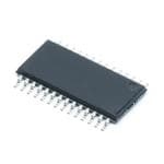
| 封装/外壳 | 28-SOIC(0.173",4.40mm 宽)裸露焊盘 |
| 封装/箱体 | HTSSOP-28 |
| 工作温度 | -40°C ~ 85°C |
| 工作温度范围 | - 40 C to + 85 C |
| 工厂包装数量 | 50 |
| 开关频率 | 700 kHz |
| 拓扑结构 | Buck |
| 最大工作温度 | + 85 C |
| 最大输入电压 | 4 V |
| 最小工作温度 | - 40 C |
| 最小输入电压 | 2.2 V |
| 标准包装 | 50 |
| 电压-输入 | 3 V ~ 4 V |
| 电压-输出 | 0.9 V ~ 2.5 V |
| 电流-输出 | 14A |
| 类型 | 降压(降压) |
| 系列 | TPS54010 |
| 设计资源 | http://www.digikey.com/product-highlights/cn/zh/texas-instruments-webench-design-center/3176 |
| 负载调节 | 0.013 % / A |
| 输出数 | 1 |
| 输出电压 | 2.5 V |
| 输出电流 | 14 A |
| 输出端数量 | 1 Output |
| 输出类型 | 可调式 |
| 配用 | /product-detail/zh/TPS54010EVM-067/296-17269-ND/679866 |
| 频率-开关 | 280kHz ~ 700kHz |


- 商务部:美国ITC正式对集成电路等产品启动337调查
- 曝三星4nm工艺存在良率问题 高通将骁龙8 Gen1或转产台积电
- 太阳诱电将投资9.5亿元在常州建新厂生产MLCC 预计2023年完工
- 英特尔发布欧洲新工厂建设计划 深化IDM 2.0 战略
- 台积电先进制程称霸业界 有大客户加持明年业绩稳了
- 达到5530亿美元!SIA预计今年全球半导体销售额将创下新高
- 英特尔拟将自动驾驶子公司Mobileye上市 估值或超500亿美元
- 三星加码芯片和SET,合并消费电子和移动部门,撤换高东真等 CEO
- 三星电子宣布重大人事变动 还合并消费电子和移动部门
- 海关总署:前11个月进口集成电路产品价值2.52万亿元 增长14.8%


PDF Datasheet 数据手册内容提取
Typical Size 6,4 mm X 9,7 mm TPS54010 www.ti.com SLVS509B–MAY2004–REVISEDJUNE2005 2.2 – 4 -V, 14-A OUTPUT SYNCHRONOUS BUCK PWM SWITCHER WITH INTEGRATED FETs (SWIFT™) FEATURES DESCRIPTION • SeparateLow-VoltagePowerBus As a member of the SWIFT™ family of dc/dc regu- • 8-mW MOSFETSwitchesforHighEfficiencyat lators, the TPS54010 low-input voltage, high-output 14-AContinuousOutput current synchronous buck PWM converter integrates all required active components. Included on the • AdjustableOutputVoltageDownto0.9V substrate with the listed features are a true, high- • ExternallyCompensatedWith1%Internal performance, voltage error amplifier that enables ReferenceAccuracy maximum performance under transient conditions • FastTransientResponse and flexibility in choosing the output filter L and C components; an undervoltage-lockout circuit to pre- • WidePWMFrequency:Adjustable280kHzto vent start-up until the VIN input voltage reaches 3 V; 700kHz aninternallyandexternallysetslowstart circuit to limit • LoadProtectedbyPeakCurrentLimitand in-rush currents; and a power-good output useful for ThermalShutdown processor/logic reset, fault signaling, and supply se- • IntegratedSolutionReducesBoardAreaand quencing. TotalCost The TPS54010 is available in a thermally enhanced • SWIFTDocumentation,ApplicationNotes,and 28-pin TSSOP (PWP) PowerPAD™ package, which DesignSoftware:www.ti.com/swift eliminatesbulkyheatsinks. APPLICATIONS • Low-Voltage,High-DensitySystemsWith PowerDistributedat2.5V,3.3VAvailable • PointofLoadRegulationforHigh- PerformanceDSPs,FPGAs,ASICs,and Microprocessors • Broadband,Networking,andOptical CommunicationsInfrastructure SIMPLIFIED SCHEMATIC EFFICIENCY 2.5 V or 3.3 V 0.68 (cid:2)H vs Input1 PVIN PH Output OUTPUT CURRENT TPS54010 100 350 (cid:2)F BOOT 0.047 (cid:2)F 200 (cid:2)F 0.1 (cid:2)F 95 PGND 3.3 V 90 Input2 VIN COMP 120 pF 85 % 1 (cid:2)F VBIAS 4.64 k(cid:1) 10 k(cid:1) y − 80 AGND VSENSE 3300 pF enc 75 422 (cid:1) Effici 70 1 (cid:2)F 65 VIN = 3.3 V, 14.7 k(cid:1) 1500 pF 60 PVIN = 2.5 V, Compensation VO = 1.5 V, Network 55 fs= 700 kHz 50 0 2 4 6 8 10 12 14 16 IO − Output Current − A Pleasebeawarethatanimportantnoticeconcerningavailability,standardwarranty,anduseincriticalapplicationsofTexas Instrumentssemiconductorproductsanddisclaimerstheretoappearsattheendofthisdatasheet. SWIFT,PowerPADaretrademarksofTexasInstruments. PRODUCTIONDATAinformationiscurrentasofpublicationdate. Copyright©2004–2005,TexasInstrumentsIncorporated Products conform to specifications per the terms of the Texas Instruments standard warranty. Production processing does not necessarilyincludetestingofallparameters.
TPS54010 www.ti.com SLVS509B–MAY2004–REVISEDJUNE2005 These devices have limited built-in ESD protection. The leads should be shorted together or the device placedinconductivefoamduringstorageorhandlingtopreventelectrostaticdamagetotheMOSgates. ORDERING INFORMATION T OUTPUTVOLTAGE PACKAGE PARTNUMBER A -40°Cto85°C Adjustibledownto0.9V PlasticHTSSOP(PWP)(1) TPS54010PWP (1) ThePWPpackageisalsoavailabletapedandreeled.AddanRsuffixtothedevicetype(i.e.,TPS54010PWPR).Seetheapplication sectionofthedatasheetforPowerPADdrawingandlayoutinformation. ABSOLUTE MAXIMUM RATINGS overoperatingfree-airtemperaturerange(unlessotherwisenoted) (1) TPS54010 UNIT SS/ENA,SYNC –0.3to7 RT –0.3to6 VI Inputvoltagerange VSENSE –0.3to4 V PVIN,VIN –0.3to4.5 BOOT –0.3to10 VBIAS,COMP,PWRGD –0.3to7 VO Outputvoltagerange V PH –0.6to6 PH Internallylimited VO Sourcecurrent COMP,VBIAS 6 mA PH 25 A IS Sinkcurrent COMP 6 mA SS/ENA,PWRGD 10 Voltagedifferential AGNDtoPGND ±0.3 V TJ Operatingjunctiontemperaturerange –40to125 °C Tstg Storagetemperaturerange –65to150 °C Leadtemperature1,6mm(1/16inch)fromcasefor10seconds 300 °C Humanbodymodel(HBM) 1.5 kV ElectrostaticDischarge(ESD)ratings CDM 750 V (1) Stressesbeyondthoselistedunder“absolutemaximumratings”maycausepermanentdamagetothedevice.Thesearestressratings only,andfunctionaloperationofthedeviceattheseoranyotherconditionsbeyondthoseindicatedunder“recommendedoperating conditions”isnotimplied.Exposuretoabsolute-maximum-ratedconditionsforextendedperiodsmayaffectdevicereliability. RECOMMENDED OPERATING CONDITIONS MIN NOM MAX UNIT VI Inputvoltage,VIN 3 4 V PowerInputvoltage,PVIN 2.2 4 V TJ Operatingjunctiontemperature –40 125 °C DISSIPATION RATINGS(1)(2) PACKAGE THERMALIMPEDANCE TA=25°C TA=70°C TA=85°C JUNCTION-TO-AMBIENT POWERRATING POWERRATING POWERRATING 28-PinPWPwithsolder 14.4°C/W 6.94W(3) 3.81W 2.77W 28-PinPWPwithoutsolder 27.9°C/W 3.58W 1.97W 1.43W (1) FormoreinformationonthePWPpackage,refertoTItechnicalbrief,literaturenumberSLMA002. (2) Testboardconditions: a.3inchx3inch,4layers,thickness:0.062inch b.1.5-oz.coppertraceslocatedonthetopofthePCB c.1.5-oz.coppergroundplaneonthebottomofthePCB d.0.5-oz.coppergroundplanesonthe2internallayers e.12thermalvias(seeRecommendedLandPatterninapplicationssectionofthisdatasheet) (3) Maximumpowerdissipationmaybelimitedbyovercurrentprotection. 2
TPS54010 www.ti.com SLVS509B–MAY2004–REVISEDJUNE2005 ELECTRICAL CHARACTERISTICS T =-40°Cto125°C,VIN=3Vto4V,PVIN=2.2Vto4V(unlessotherwisenoted) J PARAMETER TESTCONDITIONS MIN TYP MAX UNIT SUPPLYVOLTAGE,VIN VI Inputvoltage,VIN 3 4 V Supplyvoltagerange,PVIN Output=1.8V 2.2 4 V fs=350kHz,RTopen,PHpinopen,PVIN=2.5V, 6.3 10 mA SYNC=0V VIN fs=550kHz,RTopen,PHpinopen,SYNC‡ 2.5V, 8.3 13 mA PVIN=2.5V SHUTDOWN,SS/ENA=0V,PVIN=2.5V 1 1.4 mA IQ Quiescentcurrent fs=350kHz,RTopen,PHpinopen,PVIN=3.3V, 6 8 mA SYNC=0V PVIN fs=550kHz,RTopen,PHpinopen,SYNC‡ 2.5V, 6 9 mA PVIN=2.5V,VIN=3.3V SHUTDOWN,SS/ENA=0V,VIN=3.3V <140 µA UNDERVOLTAGELOCKOUT(VIN) Startthresholdvoltage,UVLO 2.95 3 V Stopthresholdvoltage,UVLO 2.7 2.8 V Hysteresisvoltage,UVLO 0.11 V Risingandfallingedgedeglitch,UVLO(1) 2.5 µs BIASVOLTAGE Outputvoltage,VBIAS I(VBIAS)=0 2.7 2.8 2.9 V Outputcurrent,VBIAS(2) 100 µA CUMULATIVEREFERENCE Vref Accuracy 0.882 0.891 0.900 V REGULATION Lineregulation(1)(3) IL=7A,fs=350kHz,TJ=85°C 0.05 %/V Loadregulation(1)(3) IL=0Ato14A,fs=350kHz,TJ=85°C 0.013 %/A PVIN=2.5V,VIN=3.3V OSCILLATOR RTopen(1),SYNC£ 0.8V 280 350 420 Internallyset—freerunningfrequency kHz RTopen(1),SYNC‡ 2.5V 440 550 660 RT=180kW (1%resistortoAGND)(1) 252 280 308 Externallyset—freerunningfrequencyrange RT=100kW (1%resistortoAGND) 460 500 540 kHz RT=68kW (1%resistortoAGND)(1) 663 700 762 High-levelthresholdvoltage,SYNC 2.5 V Low-levelthresholdvoltage,SYNC 0.8 V Pulseduration,SYNC(1) 50 ns Frequencyrange,SYNC 300 700 kHz Rampvalley(1) 0.75 V Rampamplitude(peak-to-peak)(1) 1 V Minimumcontrollableontime(1) 200 ns Maximumdutycycle(1) 90% (1) Specifiedbydesign (2) Staticresistiveloadsonly (3) SpecifiedbythecircuitusedinFigure12 3
TPS54010 www.ti.com SLVS509B–MAY2004–REVISEDJUNE2005 ELECTRICAL CHARACTERISTICS (continued) T =-40°Cto125°C,VIN=3Vto4V,PVIN=2.2Vto4V(unlessotherwisenoted) J PARAMETER TESTCONDITIONS MIN TYP MAX UNIT ERRORAMPLIFIER Erroramplifieropen-loopvoltagegain 1kW COMPtoAGND(4) 90 110 dB Erroramplifierunitygainbandwidth Parallel10kW ,160pFCOMPtoAGND(4) 3 5 MHz Erroramplifiercommonmodeinputvoltage PoweredbyinternalLDO(4) 0 VBIAS V range Inputbiascurrent,VSENSE VSENSE=Vref 60 250 nA Outputvoltageslewrate(symmetric),COMP 1 1.4 V/µs PWMCOMPARATOR PWMcomparatorpropagationdelaytime,PWM comparatorinputtoPHpin(excluding 10-mVoverdrive(4) 70 85 ns deadtime) SLOW-START/ENABLE Enablethresholdvoltage,SS/ENA 0.82 1.2 1.4 V Enablehysteresisvoltage,SS/ENA(4) 0.03 V Fallingedgedeglitch,SS/ENA(4) 2.5 µs Internalslow-starttime 2.6 3.35 4.1 ms Chargecurrent,SS/ENA SS/ENA=0V 2 5 8 µA Dischargecurrent,SS/ENA SS/ENA=0.2V,VIN=2.7V,PVIN=2.5V 1.3 2.3 4 mA POWERGOOD Power-goodthresholdvoltage VSENSEfalling 93 %Vref Power-goodhysteresisvoltage(4) 3 %Vref Power-goodfallingedgedeglitch(4) 35 µs Outputsaturationvoltage,PWRGD I(sink)=2.5mA 0.18 0.3 V Leakagecurrent,PWRGD VIN=3.3V,PVIN=2.5V 1 µA CURRENTLIMIT Currentlimit VIN=3.3V,PVIN=2.5V(4),Outputshorted 14.5 21 A Currentlimitleadingedgeblankingtime(4) 100 ns Currentlimittotalresponsetime(4) 200 ns THERMALSHUTDOWN Thermalshutdowntrippoint(4) 135 165 °C Thermalshutdownhysteresis(4) 10 °C OUTPUTPOWERMOSFETS VIN=3V,PVIN=2.5V 8 21 rDS(on) PowerMOSFETswitches mW VIN=3.6V,PVIN=2.5V 8 18 (4) Specifiedbydesign 4
TPS54010 www.ti.com SLVS509B–MAY2004–REVISEDJUNE2005 DEVICE INFORMATION PWPPACKAGE (TOPVIEW) AGND 1 28 RT VSENSE 2 27 SYNC COMP 3 26 SS/ENA PWRGD 4 25 VBIAS BOOT 5 24 VIN PH 6 23 PVIN PH 7 THERMAL 22 PVIN PH 8 PAD 21 PVIN PH 9 20 PVIN PH 10 19 PGND PH 11 18 PGND PH 12 17 PGND PH 13 16 PGND PH 14 15 PGND TERMINALFUNCTIONS PINNAME PINNUMBER DESCRIPTION Analogground.Returnforcompensationnetwork/outputdivider,slow-startcapacitor,VBIAScapacitor,and AGND 1 RTresistor.IfusingthePowerPAD,connectittoAGND.SeetheApplicationInformationsectionfor details. Bootstrapoutput.0.022-µFto0.1-µFlow-ESRcapacitorconnectedfromBOOTtoPHgeneratesfloating BOOT 5 driveforthehigh-sideFETdriver. COMP 3 Erroramplifieroutput.ConnectfrequencycompensationnetworkfromCOMPtoVSENSE Powerground.Highcurrentreturnforthelow-sidedriverandpowerMOSFET.ConnectPGNDwithlarge 15,16,17,18, PGND copperareastotheinputandoutputsupplyreturns,andnegativeterminalsoftheinputandoutput 19 capacitors.AsinglepointconnectiontoAGNDisrecommended. PH 6-14 Phaseoutput.Junctionoftheinternalhigh-sideandlow-sidepowerMOSFETs,andoutputinductor. InputsupplyforthepowerMOSFETswitchesandinternalbiasregulator.BypassthePVINpinstothe PVIN 20,21,22,23 PGNDpinsclosetodevicepackagewithahigh-quality,low-ESR10-µFceramiccapacitor. Power-goodopen-drainoutput.HighwhenVSENSE>90%V ,otherwisePWRGDislow.Notethat PWRGD 4 ref outputislowwhenSS/ENAislowortheinternalshutdownsignalisactive. RT 28 Frequencysettingresistorinput.ConnectaresistorfromRTtoAGNDtosettheswitchingfrequency,f. s Slow-start/enableinput/output.Dualfunctionpinwhichprovideslogicinputtoenable/disabledevice SS/ENA 26 operationandcapacitorinputtoexternallysetthestart-uptime. Synchronizationinput.Dualfunctionpinwhichprovideslogicinputtosynchronizetoanexternaloscillator SYNC 27 orpinselectbetweentwointernallysetswitchingfrequencies.Whenusedtosynchronizetoanexternal signal,aresistormustbeconnectedtotheRTpin. Internalbiasregulatoroutput.Suppliesregulatedvoltagetointernalcircuitry.BypassVBIASpintoAGND VBIAS 25 pinwithahigh-quality,low-ESR0.1-µFto1.0-µFceramiccapacitor. Inputsupplyfortheinternalcontrolcircuits.BypasstheVINpintothePGNDpinsclosetodevicepackage VIN 24 withahigh-quality,low-ESR1-µFceramiccapacitor. VSENSE 2 Erroramplifierinvertinginput.Connecttooutputvoltagecompensationnetwork/outputdivider. 5
TPS54010 www.ti.com SLVS509B–MAY2004–REVISEDJUNE2005 FUNCTIONALBLOCKDIAGRAM AGND VBIAS VIN VIN Enable VBIAS REG 3.0 − 4.0 V Comparator SS/ENA Falling SHUTDOWN 1.2 V Edge ILIM PVIN Deglitch Thermal Comparator 2.2 − 4.0 V Hysteresis: 0.03 V 2.5 m s Shutdown Leading 150°C Edge VIN UVLO Blanking Comparator Falling 100 ns and VIN Rising BOOT 2.95 V Edge Hysteresis: 0.11 V Deglitch 8 mW 2.5 m s SS_DIS SHUTDOWN PH LOUT VO Internal/External Slow-start + (Internal Slow-start Time = 3.35 ms − R Q Adaptive Dead-Time CO and Error S Control Logic Amplifier PWM Reference Comparator VIN VREF = 0.891 V 8 mW OSC PGND Power-Good Comparator PWRGD VSENSE Falling 0.90 Vref Edge TPS54010 Deglitch Hysteresis: 0.03 Vref SHUTDOWN 35 m s VSENSE COMP RT SYNC 6
TPS54010 www.ti.com SLVS509B–MAY2004–REVISEDJUNE2005 TYPICAL CHARACTERISTICS DRAIN-SOURCEON-STATE DRAIN-SOURCEON-STATE INTERNALLYSETOSCILLATOR RESISTANCE RESISTANCE FREQUENCY vs vs vs JUNCTIONTEMPERATURE JUNCTIONTEMPERATURE JUNCTIONTEMPERATURE 12 12 Hz 750 VIN = 3.6 V, VIN = 3.3 V, k Wn-State Resistance − 1068 PIOV =IN 9 = A 2.5 V, Wn-State Resistance − 1068 PIOV =IN 9 = A 2.5 V, scillator Frequency − 565500 SYNC ≥ 2.5 V O O O 450 Drain-Source 024 Drain-Source 024 f − Internally Set 235500 SYNC ≤ 0.8 V −40 −20 0 20 40 60 80 100 125 −40 −20 0 20 40 60 80 100 125 −40 0 25 85 125 TJ − Junction Temperature − °C TJ − Junction Temperature − °C TJ − Junction Temperature − °C Figure1. Figure2. Figure3. EXTERNALLYSETOSCILLATOR FREQUENCY VOLTAGEREFERENCE DEVICEPOWERDISSIPATION vs vs vs JUNCTIONTEMPERATURE JUNCTIONTEMPERATURE OUTPUTCURRENT Hz 800 0.895 8 − k VO = 1.5 V, y 7 VI = PVIN = 3.3 V, ernally Set Oscillator Frequenc 345670000000000 RRTT == 6180 0k WkW − Voltage Reference − VVref0000....888888997913 Device Power Dissipation − W 23456 TJ = 125°C Ext RT = 180 kW 1 f − 200−40 0 25 85 125 0.885−40 0 25 85 125 00 5 10 15 20 TJ − Junction Temperature − °C TJ − Junction Temperature − °C IO − Output Current − A Figure4. Figure5. Figure6. REFERENCEVOLTAGE INTERNALSLOWS-STARTTIME vs ERRORAMPLIFIER vs INPUTVOLTAGE OPEN-LOOPRESPONSE JUNCTIONTEMPERATURE 0.895 140 0 3.80 V PVIN = 2.5 V RL = 10 kW , −20 VIN = 3.3 V, V − Output Voltage Regulation − O0000....888888997913 Gain − dB110224680000000 GPahCTianALs =e= 2156°0C pF, −−−−−−−−111118648642000000000Phase − Degrees Internal Slow-Start Time − ms 233333......902356050505 PVIN = 2.5 V −20 −200 0.885 1 10 100 1 k 10 k 100 k 1 M 10 M 2.75 3 3.1 3.2 3.3 3.4 3.5 3.6 −40 0 25 85 125 f − Frequency − Hz VI − Input Voltage − V TJ − Junction Temperature − °C Figure7. Figure8. Figure9. 7
TPS54010 www.ti.com SLVS509B–MAY2004–REVISEDJUNE2005 APPLICATION INFORMATION PCB LAYOUT ANALOG GROUND TRACE FREQUENCY SET RESISTOR AGND RT VSENSE SYNC SLOW-START INPUT CAPACITOR BYPASS COMPENSATION CAPACITOR NETWORK COMP SS/ENA BIAS CAPACITOR PWRGD VBIAS BOOT CAPACITOR BOOT VIN EXPOSED PH POWERPAD PVIN VOUT AREA PH PVIN PH PVIN PVIN PH PH PVIN PH PGND OUTPUT INDUCTOR PGND OUTPUT FILTER PGND CAPACITOR PGND INPUT INPUT BYPASS BULK PGND CAPACITOR FILTER TOPSIDE GROUND AREA VIA to GROUND PLANE Figure10.TPS54010Layout The PVIN pins are connected together on the printed- wide trace for the analog ground signal path. This circuit board (PCB) and bypassed with a low ESR analog ground is used for the voltage set point ceramic bypass capacitor. Care should be taken to divider, timing resistor RT, slow-start capacitor, and minimize the loop area formed by the bypass capaci- bias capacitor grounds. The PH pins are tied together tor connections, the PVIN pins, and the TPS54010 and routed to the output inductor. Because the PH ground pins. The minimum recommended bypass connection is the switching node, an inductor is capacitance is a 10-µF ceramic capacitor with a X5R locatedclosetothePH pins, and the area of the PCB or X7R dielectric. The optimum placement is as close conductor is minimized to prevent excessive capaci- as possible to the PVIN pins, the AGND, and PGND tivecoupling.Connect the boot capacitor between the pins. See Figure 10 for an example of a board layout. phase node and the BOOT pin as shown in Fig- If the VIN is connected to a separate source supply, it ure 10. Keep the boot capacitor close to the IC, and is bypassed with its own capacitor. There is an area minimize the conductor trace lengths. Connect the of ground on the top layer of the PCB, directly under output filter capacitor(s) between the VOUT trace and the IC, with an exposed area for connection to the PGND. It is important to keep the loop formed by the PowerPAD. Use vias to connect this ground area to PH pins, Lout, Cout, and PGND as small as is any internal ground planes. Use additional vias at the practical. Place the compensation components from ground side of the input and output filter capacitors. the VOUT trace to the VSENSE and COMP pins. Do The AGND and PGND pins are tied to the PCB not place these components too close to the PH ground by connecting them to the ground area under trace. Due to the size of the IC package and the the device as shown in Figure 10. Use a separate device pinout, they must be routed close, but main- 8
TPS54010 www.ti.com SLVS509B–MAY2004–REVISEDJUNE2005 tain as much separation as possible while keeping ted to the largest area available. Additional areas on the layout compact. Connect the bias capacitor from the top or bottom layers also help dissipate heat, and the VBIAS pin to analog ground using the isolated any area available must be used when 6-A or greater analog ground trace. If a slow-start capacitor or RT operation is desired. Connection from the exposed resistor is used, or if the SYNC pin is used to select area of the PowerPAD to the analog ground plane 350-kHz operating frequency, connect them to this layer must be made using 0.013-inch diameter vias to trace. avoidsolderwickingthroughthevias. For operation at full rated load current, the analog Eight vias must be in the PowerPAD area with four ground plane must provide an adequate additionalviaslocatedunderthedevicepackage.The heat-dissipating area. A 3-inch by 3-inch plane of size of the vias under the package, but not in the 1-ounce copper is recommended, though not manda- exposed thermal pad area, can be increased to tory, depending on ambient temperature and airflow. 0.018. Additional vias beyond the twelve rec- Mostapplicationshavelargerareasofinternalground ommended that enhance thermal performance must plane available, and the PowerPAD must be connec- beincludedinareasnotunderthedevicepackage. Minimum Recommended Thermal Vias: 8 x 0.013 Diameter Inside 8 PL Ø0.0130 PowerPAD Area 4 x 0.018 Diameter Under Device as Shown. Additional 0.018 Diameter Vias May Be Used if Top Side Analog Ground 4 PL Ø0.0180 Area Is Extended. Connect Pin 1 to Analog Ground Plane in This Area for Optimum Performance 0.0150 0.06 0.0339 0.0650 0.0500 0.3820 0.3478 0.0500 0.2090 0.0500 0.0256 0.0650 0.0339 Minimum Recommended Exposed Copper Area for PowerPAD. 5mm 0.1700 Stencils May Require 10 Percent 0.1340 Larger Area Minimum Recommended Top Side Analog Ground Area 0.0630 0.0400 Figure11.RecommendedLandPatternfor28-PinPWPPowerPAD 9
TPS54010 www.ti.com SLVS509B–MAY2004–REVISEDJUNE2005 m F kW m F m F m F kW m F m F kW m m F m F m F kW kW kW Figure12.ApplicationCircuit,2.5Vto1.5V Figure 12 shows the schematic for a typical TPS54010 application. The TPS54010 can provide DESIGN PARAMETERS up to 14-A output current at a nominal output voltage To begin the design process, a few parameters must of 1.5 V. Nominal input voltages are 2.5 V for PVIN bedecided.Thedesignerneedstoknow: and 3.3 V for VIN. For proper thermal performance, the exposed PowerPAD underneath the device must • Inputvoltagerange besoldereddowntotheprinted-circuitboard. • Outputvoltage • Inputripplevoltage DESIGN PROCEDURE • Outputripplevoltage The following design procedure can be used to select • Outputcurrentrating component values for the TPS54010. Alternately, the • Operatingfrequency SWIFTDesignerSoftwaremaybeused to generate a completedesign.TheSWIFTDesigner Software uses For this design example, use the following as the an iterative design procedure and accesses a com- inputparameters: prehensive database of components when generating a design. This section presents a simplified dis- cussionofthedesignprocess. DESIGNPARAMETER EXAMPLEVALUE Inputvoltage(VIN) 3.3V Inputvoltagerange(PVIN) 2.2to3.5V Outputvoltage 1.5V Inputripplevoltage 300mV Outputripplevoltage 50mV Outputcurrentrating 14A 10
TPS54010 www.ti.com SLVS509B–MAY2004–REVISEDJUNE2005 (continued) I OUT(MAX) I (cid:1) DESIGNPARAMETER EXAMPLEVALUE CIN 2 (3) Operatingfrequency 700kHz In this case, the input ripple voltage would be 155 mV and the RMS ripple current would be 7 A. The SWITCHING FREQUENCY maximum voltage across the input capacitors would be Vin max plus delta Vin/2. The chosen bulk The switching frequency can be set to either one of capacitor, a Sanyo POSCAP 6TPD330M is rated for two internally programmed frequencies or set to a 6.3 V and 4.4 A of ripple current; two bypass externally programmed frequency. With the RT pin capacitors, TDK C3225X5R1C106M are each rated open, setting the SYNC pin at or above 2.5 V selects for 16 V, and the ripple current capacity is greater 550-kHz operation, whereas grounding or leaving the than 3 A at the operating frequency of 700 kHz. Total SYNC pin open selects 350-kHz operation. For this ripple current handling is in excess of 10.4 A. It is design, the switching frequency is externally pro- important that the maximum ratings for voltage and grammed using the RT pin. By connecting a resistor currentarenotexceededunderanycircumstance. (R4) from RT to AGND, any frequency in the range of 250 to 700 kHz can be set. Use Equation 1 to OUTPUT FILTER COMPONENTS determinethepropervalueofRT. R4(k(cid:1))(cid:2)500kHz(cid:1)100k(cid:1) Two components need to be selected for the output ƒs(kHz) filter, L1 and C2. Because the TPS54010 is an (1) externally compensated device, a wide range of filter In this example circuit, R4 is calculated to be 71.5 kW componenttypesandvaluescanbesupported. andtheswitchingfrequencyissetat700kHz. InductorSelection INPUT CAPACITORS To calculate the minimum value of the output induc- The TPS54010 requires an input de-coupling capaci- tor,useEquation4 tor and, depending on the application, a bulk input (cid:4) (cid:5) capacitor. The minimum value for the de-coupling VOUT(cid:1) Vin(MAX)(cid:2)VOUT cXa5pRacoitror,X7CR9,iiss 1re0coµmF.mAenhdiegdh.-qTuahleityvcoeltraagmeicratytipneg LMIN(cid:3)VIN(MAX)(cid:1)KIND(cid:1)IOUT(cid:1)Fsw (4) should be greater than the maximum input voltage. Additionally, some bulk capacitance may be needed, K is a coefficient that represents the amount of IND especially if the TPS54010 circuit is not located within inductor ripple current relative to the maximum output about 2 inches from the input voltage source. The current. For designs using low ESR output capacitors value for this capacitor is not critical but it also should such as ceramics, use K = 0.3. When using higher IND be rated to handle the maximum input voltage includ- ESR output capacitors, K = 0.2 yields better IND ing ripple voltage, and should filter the output so that results. inputripplevoltageisacceptable. For this design example, use K = 0.2 to keep the IND This input ripple voltage can be approximated by inductor ripple current small. The minimum inductor Equation2: valueiscalculatedtobe0.44µH. (cid:1)VPVIN(cid:3)IOCUBT(UMLAKX(cid:1))(cid:1)ƒs0w.25(cid:2)(cid:4)IOUT(MAX)(cid:1)ESRMAX(cid:5) FRoMrSthceuorruetnptutanfildtersaintudruactitoonr, cituirsreinmtproarttianngtsthnaottthbee exceeded. The RMS inductor current can be found (2) fromEquation5: WhereI isthemaximumloadcurrent. TtohreaTnPd,SO5UdT4e(0Mp1eA0Xn)drienqguiorenstahne ianpppulticdaeti-ocno,upalinbgulckaipnapcui-t IL(RMS)(cid:4)(cid:7)I2OUT(MAX)(cid:2)112(cid:1)(cid:12)(cid:8)(cid:9)VOUT(cid:1)VIN(M(cid:5)AVXin)((cid:1)MALXO)U(cid:3)TV(cid:1)OFUsTw(cid:6)(cid:1)0.8(cid:12)(cid:10)(cid:11)2 capacitor. ƒ is the switching frequency, C is sw (BULK) (5) the bulk capacitor value and ESR is the maximum MAX seriesresistanceofthebulkcapacitor. and the peak inductor current can be found from Equation6 The maximum RMS ripple current also needs to be checked. For worst-case conditions, this can be approximatedbyEquation3: 11
TPS54010 www.ti.com SLVS509B–MAY2004–REVISEDJUNE2005 VOUT(cid:1)(cid:5)Vin(MAX)(cid:3)VOUT(cid:6) (cid:7)VOUT(cid:1)(cid:4)VPVIN(MAX)(cid:2)VOUT(cid:5)(cid:9) 1 IL(PK)(cid:4)IOUT(MAX)(cid:2)1.6(cid:1)VIN(MAX)(cid:1)LOUT(cid:1)Fsw ICOUT(RMS)(cid:3)(cid:6)12(cid:1)(cid:11) VPVIN(MAX)(cid:1)LOUT(cid:1)Fsw (cid:11) (cid:8) (cid:10) (6) (8) For this design, the RMS inductor current is 15.4 A, The calculated RMS ripple current is 780 mA in the and the peak inductor current is 15.1 A. For this outputcapacitors. design, a Vishay IHLP2525CZ-01 style output induc- tor is specified. The largest value greater than 0.44 The maximum ESR of the output capacitor is deter- µH that meets these current requirements is 0.68 µH. mined by the amount of allowable output ripple as Increasing the inductor value decreases the ripple specified in the initial design parameters. The output current and the corresponding output ripple voltage. ripple voltage is the inductor ripple current times the The inductor value can be decreased if more margin ESR of the output filter; therefore, the maximum in the RMS current is required. In general, inductor specified ESR as listed in the capacitor data sheet is values for use with the TPS54010 falls in the range of givenbyEquation9: 0.47to2.2µH. (cid:6) (cid:8) VIN(MAX)(cid:1)LOUT(cid:1)Fsw(cid:1)0.8 CapacitorRequirements ESRMAX(cid:3)NC(cid:1)(cid:10)(cid:7)VOUT(cid:1)(cid:4)VIN(MAX)(cid:2)VOUT(cid:5)(cid:10)(cid:9)(cid:1)(cid:1)VP(cid:2)P(MAX) The important design factors for the output capacitor (9) are dc voltage rating, ripple current rating, and equivalent series resistance (ESR). The dc voltage and the maximum ESR required is 22.2 mW . A and ripple current ratings cannot be exceeded. The capacitor that meets these requirements is a Cornell ESR is important because along with the inductor Dubilier Special Polymer (SP) ESRD101M06 rated at current it determines the amount of output ripple 6.3 V with a maximum ESR of 0.015W and a ripple voltage. The actual value of the output capacitor is current rating of 2 A. An additional small 0.1-µF not critical, but some practical limits do exist. Con- ceramicbypasscapacitorC13isaalsoused. sider the relationship between the desired Other capacitor types work well with the TPS54010, closed-loop crossover frequency of the design and dependingontheneedsoftheapplication. LC corner frequency of the output filter. In general, it is desirable to keep the closed-loop crossover fre- CompensationComponents quency at less than 1/5 of the switching frequency. With high switching frequencies such as the 500 kHz The external compensation used with the TPS54010 frequency of this design, internal circuit limitations of allows for a wide range of output filter configurations. the TPS54010 limit the practical maximum crossover A large range of capacitor values and types of frequency to about 70 kHz. To allow for adequate dielectric are supported. The design example uses phase gain in the compensation network, the LC Type-3 compensation consisting of R1, R3, R5, C6, corner frequency should be about one decade or so C7, and C8. Additionally, R2 along with R1 forms a below the closed-loop crossover frequency. This voltage divider network that sets the output voltage. limits the minimum capacitor value for the output filter These component reference designators are the to: same as those used in the SWIFT Designer 2 Software. There are a number of different ways to (cid:3) (cid:4) 1 K design a compensation network. This procedure COUT(MIN)(cid:2)L (cid:1) 2(cid:1) ƒ outlines a relatively simple procedure that produces OUT CO (7) good results with most output filter combinations. Use the SWIFT Designer Software for designs with un- Where K is the frequency multiplier for the spread usually high closed-loop crossover frequencies, low between f and f . K should be between 5 and 15, LC CO value, low ESR output capacitors such as ceramics typically 10 for one decade difference. For a desired orifyouareunsureaboutthedesignprocedure. crossover of 100-kHz and a 0.68-µH inductor, the minimumvaluefortheoutput capacitor is 93 µF using When designing compensation networks for the a minimum K factor of 5. Increasing the K factor TPS54010, a number of factors need to be con- would require using a larger capacitance as 100 kHz sidered. The gain of the compensated error amplifier is approaching the maximum practical closed-loop should not be limited by the open-loop amplifier gain crossover frequency for this device. The selected characteristics and should not produce excessive output capacitor must be rated for a voltage greater gain at the switching frequency. Also, the closed-loop than the desired output voltage plus one half the crossover frequency should be set less than one-fifth ripple voltage. Any de-rating amount must also be included. The maximum RMS ripple current in the outputcapacitorsisgivenbyEquation8: 12
TPS54010 www.ti.com SLVS509B–MAY2004–REVISEDJUNE2005 ƒ of the switching frequency, and the phase margin at ƒ (cid:2) CO crossover must be greater than 45 degrees. The INT V (cid:1)2 general procedure outlined here produces results IN(MAX) (17) consistent with these requirements without going into AndthevalueforC6isgivenbyEquation18: greatdetailaboutthetheoryofloopcompensation. First, calculate the output filter LC corner frequency C6(cid:1)2(cid:1)R11ƒ usingEquation10: INT (18) ƒ 1 The first zero, f is located at one-half the output LC(cid:1)2(cid:1)(cid:2)L C filter LC corner fZr1equency; so, R3 can be calculated OUT OUT (10) from: Forthedesignexample,fLC=19.3kHz. R3(cid:1) 1 (cid:1)C6ƒ The closed-loop crossover frequency should be LC (19) chosen to be greater than f and less than one-fifth LC The second zero, f is located at the output filter LC of the switching frequency. Also, the crossover fre- Z2 cornerfrequency;so,C8canbecalculatedfrom: quency should not exceed 150 kHz, as the error amplifier may not provide the desired gain. For this C8(cid:1) 1 design, a crossover frequency of 100 kHz was 2(cid:1)R1ƒLC (20) chosen. This value is chosen for comparatively wide loopbandwidthwhile still allowing for adequate phase The first pole, f is located to coincide with output P1 boosttoinsurestability. filterESRzerofrequency.Thisfrequencyisgivenby: Next, calculate the R2 resistor value for the output ƒ (cid:1) 1 ESR0 2(cid:1)R C voltageof1.5VusingEquation11: ESR OUT (21) R2(cid:3) R1(cid:1)0.891 where R is the equivalent series resistance of the V (cid:2)0.891 ESR OUT (11) outputcapacitor. For any TPS54010 design, start with an R1 value of In this case, the ESR zero frequency is 88.4 kHz, and 10kW .R2is14.7kW . R5canbecalculatedfrom: Now, the values for the compensation components R5(cid:1) 1 2(cid:1)C8ƒ that set the poles and zeros of the compensation ESR (22) network can be calculated. Assuming that R1 >> than The final pole is placed at a frequency above the R5 and C6 >> C7, the pole and zero locations are closed-loop crossover frequency high enough to not givenbyEquation12throughEquation18: cause the phase to decrease too much at the ƒ (cid:1) 1 crossover frequency while still providing enough at- Z1 2(cid:1)R3C6 (12) tenuation so that there is little or no gain at the ƒ (cid:1) 1 switching frequency. The f pole location for this Z2 2(cid:1)R1C8 (13) circuit is set to 3.5 times thPe2 closed-loop crossover ƒ (cid:1) 1 frequency and the last compensation component P1 2(cid:1)R5C8 (14) valueC7canbederived: ƒ (cid:1) 1 C7(cid:1) 1 P2 2(cid:1)R3C7 (15) 7(cid:1)R3ƒ CO (23) Additionally, there is a pole at the origin, which has Note that capacitors are only available in a limited unitygainatafrequency: range of standard values, so the nearest standard ƒ (cid:1) 1 value has been chosen for each capacitor. The INT 2(cid:1)R1C6 (16) measured closed-loop response for this design is showninFigure5. This pole is used to set the overall gain of the compensated error amplifier and determines the BIAS AND BOOTSTRAP CAPACITORS closed-loop crossover frequency. Because R1 is given as 1 kW and the crossover frequency is Every TPS54010 design requires a bootstrap capaci- selected as 100 kHz, the desired f can be calcu- INT tor, C3, and a bias capacitor, C4. The bootstrap latedfromEquation17: capacitor must be a 0.1 µF. The bootstrap capacitor is located between the PH pins and BOOT. The bias capacitor is connected between the VBIAS pin and 13
TPS54010 www.ti.com SLVS509B–MAY2004–REVISEDJUNE2005 AGND. The value should be 1.0 µF. Both capacitors SNUBBER CIRCUIT should be high-quality ceramic types with X7R or R10 and C11 of the application schematic comprise a X5R grade dielectric for temperature stability. They snubber circuit. The snubber is included to reduce should be placed as close to the device connection overshoot and ringing on the phase node when the pinsaspossible. internal high-side FET turns on. Because the fre- quency and amplitude of the ringing depends to a POWER GOOD large degree on parasitic effects, it is best to choose The TPS54010 is provided with a power-good output these component values based on actual measure- pin PWRGD. This output is an open-drain output and ments of any design layout. See literature number is intended to be pulled up to a 3.3-V or 5-V logic SLUP100 for more detailed information on snubber supply.A10-kW pullupworkswellinthisapplication. design. m kW m m m 71.5 kW m F m F kW m m F m F m F W 14.7 kW 10 kW The following part numbers are used for test purposes: C1 = T520D337M0O4ASE015 (Kemet) C2 = TDK C3225X5R0J107M ceramic 6.3 V X5R L1 = IHLP2525CZ−01 0.68 m H (Vishay Dale) Figure13.1.5-VPowerSupplyWithCeramicOutputCapacitors Figure 13 shows an application where all ceramic are used. The compensation network components capacitors, including the main output filter capacitor, werecalculatedusingSWIFTDesigner Software. See Figure 22 through Figure 30 for loop response, performance graphs, and switching waveforms for thiscircuit. 14
TPS54010 www.ti.com SLVS509B–MAY2004–REVISEDJUNE2005 m F m F m F kW m F m m F 10 kW m F m F m F 20 kW 10 kW 10 kW 49.9 W 10 kW 2 kW 10 kW 49.9 W 10 kW 14.7 kW m F Figure14.1.5-VPowerSupplyWithRemoteSense With an output current of 14 A, if the load is located sates for voltage drops in both the output voltage rail far from the dc/dc converter circuit, it may be ben- and the return (GND). The difference amplifier of U2 eficial to include a remote sense capability. Figure 14 forces the output of the TPS54010 to generate an is an example of a power supply incorporating active output voltage that maintains a constant 1.5-V differ- differential remote sensing. As the TPS54010 only ence between +1.5V_REMOTE_SENSE and has a positive VSENSE input, this circuit compen- -1.5V_REMOTE_SENSE. 15
TPS54010 www.ti.com SLVS509B–MAY2004–REVISEDJUNE2005 3.6 V 100 nF 330 m F 10 m F 10 m F C17 1 m F 100 nF 0.047 m F 10 kW 1 m F 0.68 m H 0.047 m F 100 m F 100 m F 0.1 m F 2.4 kW 422 W 14.7 kW 10 kW Figure15.2.5Vto1.5VPowerSupplywithChargePump If a suitable 3-V to 4-V source is not available for the VIN supply, a charge pump may be used to boost the PVIN voltage.Inthiscircuit,thechargepumpisusedtoboosta2.5-Vsourcetoanominal3.6V. 16
TPS54010 www.ti.com SLVS509B–MAY2004–REVISEDJUNE2005 PERFORMANCE GRAPHS The performance data for Figure 16 through Figure 24 are for the circuit in Figure 12. Conditions are PVIN = 2.5 V,VIN=3.3V,V =1.5V,f =700kHz,andI =7A,T =25°C,unlessotherwisespecified. O s O A MEASUREDLOOPRESPONSE LOADREGULATION LINEREGULATION vs vs vs FREQUENCY OUTPUTCURRENT INPUTVOLTAGE 60 180 0.5 0.3 Phase 0.4 0.25 40 120 % 0.3 % 0.2 IO = 0A Gain - dB-22000 Gain -06600 Phase - Degrees ut Voltage Variation - --0000....21120 3.32 .V2 V 2.5 V4.0 V ut Voltage Deviation - -0-00.0..0001..515510 IIOO == 174AA -40 -120 Outp -0.3 Outp -0-.01.52 -0.4 -0.25 -60 -180 -0.5 -0.3 100 1 k 10 k 100 k 1 M 0 2 4 6 8 10 12 14 16 2 2.5 3 3.5 4 f - Frequency - Hz IO - Output - A PVIN - V Figure16. Figure17. Figure18. EFFICIENCY vs OUTPUTCURRENT INPUTRIPPLEVOLTAGE OUTPUTVOLTAGERIPPLE 100 2.2 V PVIN(RIPPLE) = 100 mV/div (ac coupled) VO(RIPPLE) = 20 mV/div (ac coupled) 95 3.3 V 90 85 2.5 V % y - 80 nc75 4.0 V e Effici70 65 60 55 IO = 14 A V(PH) = 1 V/div IO = 14 A V(PH ) = 1 V/div 50 0 2 4 6 8 10 12 14 16 Time = 500 nsec/div Time = 500 nsec/div IO - Output - A Figure19. Figure20. Figure21. START-UPWAVEFORM START-UPWAVEFORM OUTPUTVOLTAGERELATIVE OUTPUTVOLTAGERELATIVE LOADTRANSIENTRESPONSE TOENABLE TOVIN VO = 50 mV/div (ac coupled) V(SS/ENA) = 1 V/div VIN = 1 V/div IO = 5 A/div VO = 1 V/div VO = 1 V/div Time = 200(cid:0)(cid:2)sec/div Time = 10 msec/div Time = 10 msec/div Figure22. Figure23. Figure24. 17
TPS54010 www.ti.com SLVS509B–MAY2004–REVISEDJUNE2005 PERFORMANCE GRAPHS The performance data for Figure 25 through Figure 34 are for the circuit in Figure 13. Conditions are PVIN = 2.5 V,VIN=3.3V,V =1.5V,f =700kHz,andI =7A,T =25°C,unlessotherwisespecified. O s O A FREE-AIRTEMPERATURE MEASUREDLOOPRESPONSE LOADREGULATION vs vs vs MAXIMUMOUTPUTCURRENT FREQUENCY OUTPUTCURRENT 125 60 180 0.5 115 VO = 1.5 V, Phase 0.4 °− Free-Air Temperature −CA 10345678955555555 Safe Operating AreaPTJV I=N 1 =2 5V°IC = 3.3 V, Gain - dB--242400000 Gain --06161020200Phase - Degrees Output Voltage Variation - % ---000000......3211230 3.32 .V2 V 2.5 V4.0 V T 25 -0.4 -60 -180 150 1 2 3 4 5 6 7 8 9 101112131415 100 1 k 10 k 100 k 1 M -0.5 0 2 4 6 8 10 12 14 16 IO − Output Current − A f - Frequency - Hz IO - Output Current - A Note: Figure 25 applies to the application circuit (Figure 13) installed on a 3 inch x 3 inch x 0.062 inch four-layer PCB. Figure25. Figure26. Figure27. LINEREGULATION EFFICIENCY vs vs PVIN OUTPUTCURRENT INPUTRIPPLEVOLTAGE 0.3 100 PVIN(RIPPLE) = 100 mV/div (ac coupled) 2.2 V 0.25 95 % 0.2 IO = 0A 90 3.3 V n - 0.15 o 85 2.5 V Deviati 0.00.51 IO = 7A y - %80 ut Voltage -0-.00.510 IO = 14A Efficienc677505 4.0 V Outp -0-.01.52 60 -0.25 55 IO = 14 A V(PH) = 1 V/div -0.3 50 2 2.5 3 3.5 4 0 2 4 6 8 10 12 14 16 Time = 500 nsec/div PVIN - V IO - Output Current - A Figure28. Figure29. Figure30. 18
TPS54010 www.ti.com SLVS509B–MAY2004–REVISEDJUNE2005 PERFORMANCE GRAPHS (continued) START-UPWAVEFORM OUTPUTVOLTAGERELATIVE OUTPUTVOLTAGERIPPLE LOADTRANSIENTRESPONSE TOENABLE VO(RIPPLE) = 10 mV/div (ac coupled) VO = 100 mV/div (ac coupled) V(SS/ENA) = 1 V/div IO = 5 A/div VO = 1 V/div IO = 14 A V(PH ) = 1 V/div Time = 500 nsec/div Time = 200 (cid:1)sec/div Time = 10 msec/div Figure31. Figure32. Figure33. START-UPWAVEFORM OUTPUTVOLTAGERELATIVE TOENABLE VIN = 1 V/div VO = 1 V/div Time = 10 msec/div Figure34. NOTE: DETAILED DESCRIPTION If the PVIN input is controlled via a fast bus switch, it OPERATING WITH SEPARATE PVIN results in a hard-start condition and may damage the load (i.e., whatever is connected to the regulated The TPS54010 is designed to operate with the power output of the TPS54010). If a power-good signal is stage (high-side and low-side MOSFETs) and the not available from the 2.5-V power supply, one can PVIN input connected to a separate power source be generated using a comparator and hold the from VIN. The primary intended application has VIN SS/ENA pin low until the 2.5-V bus power is good. An connected to a 3.3-V bus and PVIN connected to a example of this is shown in Figure 35. This circuit can 2.5-V bus. The TPS54010 cannot be damaged by also be used to prevent the TPS54010 output from any sequencing of these voltages. However, the following the PVIN input while the PVIN power supply UVLO (see detailed description section) is referenced isrampingup. to the VIN input. Some conditions may cause unde- sirableoperation. If PVIN is absent when the VIN input is high, the slow-start is released, and the PWM circuit goes to maximum duty factor. When the PVIN input ramps up, the output of the TPS54010 follows the PVIN inputuntilenoughvoltageispresenttoregulateto the properoutputvalue. 19
TPS54010 www.ti.com SLVS509B–MAY2004–REVISEDJUNE2005 the UVLO comparator, and a 2.5-ms rising and falling 100 kW edge deglitch circuit reduce the likelihood of shutting the device down due to noise on VIN. UVLO is with VIN 10 kW respect to VIN and not PVIN, see the Application PVIN + VBIAS − SS/ENA Informationsection. 10 kW 27.4 kW 1/2 LM293 SLOW-START/ENABLE (SS/ENA) Figure35.UndervoltageLockoutCircuitforPVIN The slow-start/enable pin provides two functions. UsingOpen-CollectororOpen-DrainComparator First, the pin acts as an enable (shutdown) control by keeping the device turned off until the voltage ex- ceeds the start threshold voltage of approximately PVIN and VIN can be tied together for 3.3-V bus 1.2 V. When SS/ENA exceeds the enable threshold, operation. device start-up begins. The reference voltage fed to the error amplifier is linearly ramped up from 0 V to MAXIMUM OUTPUT VOLTAGE 0.891 V in 3.35 ms. Similarly, the converter output The maximum attainable output voltage is limited by voltage reaches regulation in approximately 3.35 ms. the minimum voltage at the PVIN pin. Nominal Voltage hysteresis and a 2.5-ms falling edge deglitch maximum duty cycle is limited to 90% in the circuit reduce the likelihood of triggering the enable TPS54010;so,maximumoutputvoltageis: duetonoise. V (cid:2)PVIN (cid:1)0.9 O(max) (min) The second function of the SS/ENA pin provides an (24) external means of extending the slow-start time with Care must be taken while operating when nominal a low-value capacitor connected between SS/ENA conditions cause duty cycles near 90%. Load transi- andAGND. ents can require momentary increases in duty cycle. Adding a capacitor to the SS/ENA pin has two effects If the required duty cycle exceeds 90%, the output on start-up. First, a delay occurs between release of mayfalloutofregulation. the SS/ENA pin and start-up of the output. The delay is proportional to the slow-start capacitor value and GROUNDING AND PowerPAD LAYOUT lasts until the SS/ENA pin reaches the enable The TPS54010 has two internal grounds (analog and threshold.Thestart-updelayisapproximately: power). Inside the TPS54010, the analog ground ties 1.2 V to all of the noise-sensitive signals, whereas the t (cid:2)C (cid:1) d (SS) 5 (cid:1)A power ground ties to the noisier power signals. The (25) PowerPAD must be tied directly to AGND. Noise Second, as the output becomes active, a brief injected between the two grounds can degrade the ramp-up at the internal slow-start rate may be ob- performance of the TPS54010, particularly at higher served before the externally set slow-start rate takes output currents. However, ground noise on an analog control and the output rises at a rate proportional to ground plane can also cause problems with some of the slow-start capacitor. The slow-start time set by the control and bias signals. For these reasons, thecapacitorisapproximately: separate analog and power ground planes are rec- 0.7 V ommended. These two planes must tie together t (cid:2)C (cid:1) directly at the IC to reduce noise between the two (SS) (SS) 5 (cid:1)A (26) grounds. The only components that must tie directly The actual slow-start time is likely to be less than the tothepowerground plane are the input capacitor, the above approximation due to the brief ramp-up at the output capacitor, the input voltage decoupling capaci- internalrate. tor,andthePGNDpinsoftheTPS54010. VBIAS REGULATOR (VBIAS) UNDERVOLTAGE LOCKOUT (UVLO) The VBIAS regulator provides internal analog and The TPS54010 incorporates an undervoltage-lockout digital blocks with a stable supply voltage over circuit to keep the device disabled when the input variationsinjunctiontemperatureandinputvoltage.A voltage (VIN) is insufficient. During power up, internal high-quality, low-ESR, ceramic bypass capacitor is circuits are held inactive until VIN exceeds the required on the VBIAS pin. X7R or X5R grade nominal UVLO threshold voltage of 2.95 V. Once the dielectrics are recommended because their values UVLO start threshold is reached, device start-up are more stable over temperature. The bypass ca- begins. The device operates until VIN falls below the pacitor must be placed close to the VBIAS pin and nominal UVLO stop threshold of 2.8 V. Hysteresis in returnedtoAGND. 20
TPS54010 www.ti.com SLVS509B–MAY2004–REVISEDJUNE2005 External loading on VBIAS is allowed, with the ERROR AMPLIFIER caution that internal circuits require a minimum The high-performance, wide bandwidth, voltage error VBIAS of 2.7 V, and external loads on VBIAS with ac amplifier sets the TPS54010 apart from most dc/dc or digital-switching noise may degrade performance. converters. The user is given the flexibility to use a The VBIAS pin may be useful as a reference voltage wide range of output L and C filter components to suit for external circuits. VBIAS is derived from the VIN the particular application needs. Type-2 or Type-3 pin; see the functional block diagram of this data compensation can be employed using external com- sheet. pensationcomponents. VOLTAGE REFERENCE PWM CONTROL The voltage reference system produces a precise V ref Signals from the error amplifier output, oscillator, and signal by scaling the output of a temperature stable current limit circuit are processed by the PWM control bandgap circuit. During manufacture, the bandgap logic. Referring to the internal block diagram, the and scaling circuits are trimmed to produce 0.891 V control logic includes the PWM comparator, OR gate, at the output of the error amplifier, with the amplifier PWM latch, and portions of the adaptive dead-time connected as a voltage follower. The trim procedure and control-logic block. During steady-state operation adds to the high-precision regulation of the below the current limit threshold, the PWM TPS54010, because it cancels offset errors in the comparator output and oscillator pulse train alter- scaleanderroramplifiercircuits. nately reset and set the PWM latch. Once the PWM latch is set, the low-side FET remains on for a OSCILLATOR AND PWM RAMP minimum duration set by the oscillator pulse width. The oscillator frequency is set to an internally fixed During this period, the PWM ramp discharges rapidly value of 350 kHz. The oscillator frequency can be to its valley voltage. When the ramp begins to charge externally adjusted from 280 to 700 kHz by con- back up, the low-side FET turns off and high-side necting a resistor between the RT pin to ground. The FET turns on. As the PWM ramp voltage exceeds the switching frequency is approximated by the following error amplifier output voltage, the PWM comparator equation, where R is the resistance from RT to resets the latch, thus turning off the high-side FET AGND: and turning on the low-side FET. The low-side FET SwitchingFrequency(cid:2)100k(cid:1)(cid:1)500[kHz] remains on until the next oscillator pulse discharges the PWM ramp. During transient conditions, the error R (27) amplifier output could be below the PWM ramp valley External synchronization of the PWM ramp is poss- voltage or above the PWM peak voltage. If the error ible over the frequency range of 330 kHz to 700 kHz amplifier is high, the PWM latch is never reset, and by driving a synchronization signal into SYNC and thehigh-sideFETremainsonuntil the oscillator pulse connecting a resistor from RT to AGND. Choose a signals the control logic to turn the high-side FET off resistor between the RT and AGND which sets the and the low-side FET on. The device operates at its free running frequency to 80% of the synchronization maximum duty cycle until the output voltage rises to signal. The following table summarizes the frequency the regulation set-point, setting VSENSE to approxi- selectionconfigurations: mately the same voltage as VREF. If the error amplifier output is low, the PWM latch is continually SWITCHING SYNCPIN RTPIN FREQUENCY reset and the high-side FET does not turn on. The low-side FET remains on until the VSENSE voltage 350kHz,internally FloatorAGND Float decreases to a range that allows the PWM set comparator to change states. The TPS54010 is 550kHz,internally ‡ 2.5V Float capable of sinking current continuously until the set outputreachestheregulationset-point. Externallyset280 Float R=180kW to68kW kHzto700kHz If the current limit comparator trips for longer than Externally Synchronization R=RTvaluefor80% 100 ns, the PWM latch resets before the PWM ramp synchronizedfre- signal ofexternal exceeds the error amplifier output. The high-side FET quency synchronizationfre- turns off and low-side FET turns on to decrease the quency energy in the output inductor and consequently the output current. This process is repeated each cycle in whichthecurrentlimitcomparatoristripped. 21
TPS54010 www.ti.com SLVS509B–MAY2004–REVISEDJUNE2005 DEAD-TIME CONTROL AND MOSFET THERMAL SHUTDOWN DRIVERS The device uses the thermal shutdown to turn off the Adaptive dead-time control prevents shoot-through power MOSFETs and disable the controller if the current from flowing in both N-channel power junction temperature exceeds 150°C. The device is MOSFETs during the switching transitions by actively released from shutdown automatically when the junc- controlling the turn-on times of the MOSFET drivers. tion temperature decreases to 10°C below the ther- The high-side driver does not turn on until the voltage mal shutdown trip point, and starts up under control at the gate of the low-side FET is below 2 V. While oftheslow-startcircuit. the low-side driver does not turn on until the voltage Thermal shutdown provides protection when an over- atthegateofthehigh-sideMOSFETisbelow2V. load condition is sustained for several milliseconds. The high-side and low-side drivers are designed with With a persistent fault condition, the device cycles 300-mAsourceandsinkcapabilityto quickly drive the continuously; starting up by control of the slow-start power MOSFETs gates. The low-side driver is sup- circuit, heating up due to the fault condition, and then plied from VIN, whereas the high-side driver is shutting down on reaching the thermal shutdown trip supplied from the BOOT pin. A bootstrap circuit uses point. This sequence repeats until the fault condition an external BOOT capacitor and an internal 2.5-W isremoved. bootstrap switch connected between the VIN and BOOT pins. The integrated bootstrap switch improves POWER-GOOD (PWRGD) drive efficiency and reduces external component The power-good circuit monitors for undervoltage count. conditions on VSENSE. If the voltage on VSENSE is 10% below the reference voltage, the open-drain OVERCURRENT PROTECTION PWRGD output is pulled low. PWRGD is also pulled The cycle-by-cycle current limiting is achieved by low if VIN is less than the UVLO threshold or SS/ENA sensing the current flowing through the high-side is low. When VIN, UVLO threshold, SS/ENA, enable MOSFET and comparing this signal to a preset threshold, and VSENSE > 90% of Vref, the overcurrent threshold. The high-side MOSFET is open-drain output of the PWRGD pin is high. A turned off within 200 ns of reaching the current limit hysteresis voltage equal to 3% of V and a 35-µs ref threshold. A 100-ns leading-edge blanking circuit falling-edge deglitch circuit prevent tripping of the prevents current limit false tripping. Current limit power-goodcomparatorduetohigh-frequencynoise. detection occurs only when current flows from VIN to PH when sourcing current to the output filter. Load protectionduringcurrent sink operation is provided by thermalshutdown. 22
None
PACKAGE OPTION ADDENDUM www.ti.com 11-Apr-2013 PACKAGING INFORMATION Orderable Device Status Package Type Package Pins Package Eco Plan Lead/Ball Finish MSL Peak Temp Op Temp (°C) Top-Side Markings Samples (1) Drawing Qty (2) (3) (4) TPS54010PWP ACTIVE HTSSOP PWP 28 50 Green (RoHS CU NIPDAU Level-2-260C-1 YEAR -40 to 85 TPS54010 & no Sb/Br) TPS54010PWPG4 ACTIVE HTSSOP PWP 28 50 Green (RoHS CU NIPDAU Level-2-260C-1 YEAR -40 to 85 TPS54010 & no Sb/Br) TPS54010PWPR ACTIVE HTSSOP PWP 28 2000 Green (RoHS CU NIPDAU Level-2-260C-1 YEAR -40 to 85 TPS54010 & no Sb/Br) TPS54010PWPRG4 ACTIVE HTSSOP PWP 28 2000 Green (RoHS CU NIPDAU Level-2-260C-1 YEAR -40 to 85 TPS54010 & no Sb/Br) (1) The marketing status values are defined as follows: ACTIVE: Product device recommended for new designs. LIFEBUY: TI has announced that the device will be discontinued, and a lifetime-buy period is in effect. NRND: Not recommended for new designs. Device is in production to support existing customers, but TI does not recommend using this part in a new design. PREVIEW: Device has been announced but is not in production. Samples may or may not be available. OBSOLETE: TI has discontinued the production of the device. (2) Eco Plan - The planned eco-friendly classification: Pb-Free (RoHS), Pb-Free (RoHS Exempt), or Green (RoHS & no Sb/Br) - please check http://www.ti.com/productcontent for the latest availability information and additional product content details. TBD: The Pb-Free/Green conversion plan has not been defined. Pb-Free (RoHS): TI's terms "Lead-Free" or "Pb-Free" mean semiconductor products that are compatible with the current RoHS requirements for all 6 substances, including the requirement that lead not exceed 0.1% by weight in homogeneous materials. Where designed to be soldered at high temperatures, TI Pb-Free products are suitable for use in specified lead-free processes. Pb-Free (RoHS Exempt): This component has a RoHS exemption for either 1) lead-based flip-chip solder bumps used between the die and package, or 2) lead-based die adhesive used between the die and leadframe. The component is otherwise considered Pb-Free (RoHS compatible) as defined above. Green (RoHS & no Sb/Br): TI defines "Green" to mean Pb-Free (RoHS compatible), and free of Bromine (Br) and Antimony (Sb) based flame retardants (Br or Sb do not exceed 0.1% by weight in homogeneous material) (3) MSL, Peak Temp. -- The Moisture Sensitivity Level rating according to the JEDEC industry standard classifications, and peak solder temperature. (4) Multiple Top-Side Markings will be inside parentheses. Only one Top-Side Marking contained in parentheses and separated by a "~" will appear on a device. If a line is indented then it is a continuation of the previous line and the two combined represent the entire Top-Side Marking for that device. Important Information and Disclaimer:The information provided on this page represents TI's knowledge and belief as of the date that it is provided. TI bases its knowledge and belief on information provided by third parties, and makes no representation or warranty as to the accuracy of such information. Efforts are underway to better integrate information from third parties. TI has taken and continues to take reasonable steps to provide representative and accurate information but may not have conducted destructive testing or chemical analysis on incoming materials and chemicals. TI and TI suppliers consider certain information to be proprietary, and thus CAS numbers and other limited information may not be available for release. In no event shall TI's liability arising out of such information exceed the total purchase price of the TI part(s) at issue in this document sold by TI to Customer on an annual basis. Addendum-Page 1
PACKAGE OPTION ADDENDUM www.ti.com 11-Apr-2013 OTHER QUALIFIED VERSIONS OF TPS54010 : •Enhanced Product: TPS54010-EP NOTE: Qualified Version Definitions: •Enhanced Product - Supports Defense, Aerospace and Medical Applications Addendum-Page 2
PACKAGE MATERIALS INFORMATION www.ti.com 12-Feb-2019 TAPE AND REEL INFORMATION *Alldimensionsarenominal Device Package Package Pins SPQ Reel Reel A0 B0 K0 P1 W Pin1 Type Drawing Diameter Width (mm) (mm) (mm) (mm) (mm) Quadrant (mm) W1(mm) TPS54010PWPR HTSSOP PWP 28 2000 330.0 16.4 6.9 10.2 1.8 12.0 16.0 Q1 PackMaterials-Page1
PACKAGE MATERIALS INFORMATION www.ti.com 12-Feb-2019 *Alldimensionsarenominal Device PackageType PackageDrawing Pins SPQ Length(mm) Width(mm) Height(mm) TPS54010PWPR HTSSOP PWP 28 2000 350.0 350.0 43.0 PackMaterials-Page2
GENERIC PACKAGE VIEW PWP 28 PowerPADTM TSSOP - 1.2 mm max height 4.4 x 9.7, 0.65 mm pitch SMALL OUTLINE PACKAGE Images above are just a representation of the package family, actual package may vary. Refer to the product data sheet for package details. 4224765/A www.ti.com
None
None
IMPORTANTNOTICEANDDISCLAIMER TIPROVIDESTECHNICALANDRELIABILITYDATA(INCLUDINGDATASHEETS),DESIGNRESOURCES(INCLUDINGREFERENCE DESIGNS),APPLICATIONOROTHERDESIGNADVICE,WEBTOOLS,SAFETYINFORMATION,ANDOTHERRESOURCES“ASIS” ANDWITHALLFAULTS,ANDDISCLAIMSALLWARRANTIES,EXPRESSANDIMPLIED,INCLUDINGWITHOUTLIMITATIONANY IMPLIEDWARRANTIESOFMERCHANTABILITY,FITNESSFORAPARTICULARPURPOSEORNON-INFRINGEMENTOFTHIRD PARTYINTELLECTUALPROPERTYRIGHTS. TheseresourcesareintendedforskilleddevelopersdesigningwithTIproducts.Youaresolelyresponsiblefor(1)selectingtheappropriate TIproductsforyourapplication,(2)designing,validatingandtestingyourapplication,and(3)ensuringyourapplicationmeetsapplicable standards,andanyothersafety,security,orotherrequirements.Theseresourcesaresubjecttochangewithoutnotice.TIgrantsyou permissiontousetheseresourcesonlyfordevelopmentofanapplicationthatusestheTIproductsdescribedintheresource.Other reproductionanddisplayoftheseresourcesisprohibited.NolicenseisgrantedtoanyotherTIintellectualpropertyrightortoanythird partyintellectualpropertyright.TIdisclaimsresponsibilityfor,andyouwillfullyindemnifyTIanditsrepresentativesagainst,anyclaims, damages,costs,losses,andliabilitiesarisingoutofyouruseoftheseresources. TI’sproductsareprovidedsubjecttoTI’sTermsofSale(www.ti.com/legal/termsofsale.html)orotherapplicabletermsavailableeitheron ti.comorprovidedinconjunctionwithsuchTIproducts.TI’sprovisionoftheseresourcesdoesnotexpandorotherwisealterTI’sapplicable warrantiesorwarrantydisclaimersforTIproducts. MailingAddress:TexasInstruments,PostOfficeBox655303,Dallas,Texas75265 Copyright©2019,TexasInstrumentsIncorporated