ICGOO在线商城 > 集成电路(IC) > PMIC - LED 驱动器 > TPS61040QDBVRQ1

 Datasheet下载
- 型号: TPS61040QDBVRQ1
- 制造商: Texas Instruments
- 库位|库存: xxxx|xxxx
- 要求:
| 数量阶梯 | 香港交货 | 国内含税 |
| +xxxx | $xxxx | ¥xxxx |
查看当月历史价格
查看今年历史价格
TPS61040QDBVRQ1产品简介:
ICGOO电子元器件商城为您提供TPS61040QDBVRQ1由Texas Instruments设计生产,在icgoo商城现货销售,并且可以通过原厂、代理商等渠道进行代购。 TPS61040QDBVRQ1价格参考。Texas InstrumentsTPS61040QDBVRQ1封装/规格:PMIC - LED 驱动器, LED 驱动器 IC 1 输出 DC DC 稳压器 升压 400mA(开关) SOT-23-5。您可以下载TPS61040QDBVRQ1参考资料、Datasheet数据手册功能说明书,资料中有TPS61040QDBVRQ1 详细功能的应用电路图电压和使用方法及教程。
TPS61040QDBVRQ1 是德州仪器(Texas Instruments)生产的一款PMIC(电源管理集成电路)LED驱动器。该芯片专为高效、紧凑的升压转换器设计,适用于多种便携式设备和低功耗应用。以下是其主要应用场景:

 1. 便携式电子设备
TPS61040QDBVRQ1 常用于便携式电子设备中,如智能手机、平板电脑、智能手表等。这些设备通常需要在电池供电的情况下驱动高亮度LED背光或指示灯。TPS61040QDBVRQ1 的高效升压功能可以将较低的输入电压(如锂电池的3.6V)提升到更高的输出电压(最高可达28V),从而确保LED能够获得足够的电流以保持亮度。

 2. 显示屏背光驱动
在中小尺寸的液晶显示器(LCD)中,LED背光是提高显示效果的关键组件。TPS61040QDBVRQ1 可以为这些背光系统提供稳定的电流驱动,确保显示屏在不同亮度设置下都能保持一致的色彩和亮度表现。它支持高达250mA的连续输出电流,适合驱动多个串联或并联的LED。

 3. 汽车电子
在汽车内部照明系统中,TPS61040QDBVRQ1 可以用于驱动仪表盘、中控台、车门装饰条等位置的LED灯。它能够在宽范围的输入电压下稳定工作(2.7V至5.5V),并且具有良好的抗电磁干扰(EMI)性能,符合汽车电子的严格要求。此外,它还具备过流保护、短路保护等功能,确保系统的安全性。

 4. 工业控制与自动化
在工业环境中,TPS61040QDBVRQ1 可用于驱动状态指示灯、报警灯等。它的小型封装(QFN-16,4mm x 4mm)使得它可以轻松集成到紧凑的电路板上,同时其高效的升压转换能力有助于降低系统的功耗,延长电池寿命。

 5. 智能家居与物联网(IoT)设备
在智能家居和物联网设备中,TPS61040QDBVRQ1 可以为各种传感器、摄像头、显示器等提供LED驱动功能。例如,在智能门铃、安防摄像头中,它可以驱动红外LED用于夜间监控,或者驱动可见光LED用于状态指示。

总的来说,TPS61040QDBVRQ1 凭借其高效、紧凑的设计和广泛的工作电压范围,适用于多种需要LED驱动的应用场景,特别是在对功耗和空间有严格要求的便携式和嵌入式系统中。
| 参数 | 数值 |
| 产品目录 | 集成电路 (IC)光电子产品 |
| 描述 | IC LED DRVR WHITE BCKLGT SOT23-5LED照明驱动器 Auto Cat Low Pwr DC/DC Boost Cnvrtr |
| 产品分类 | |
| 品牌 | Texas Instruments |
| 产品手册 | |
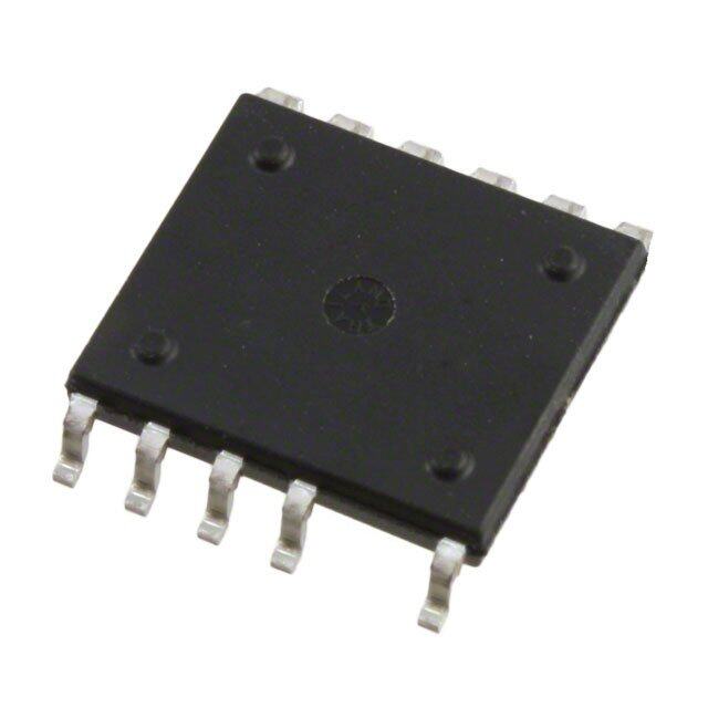
| 产品图片 |
|
| rohs | 符合RoHS无铅 / 符合限制有害物质指令(RoHS)规范要求 |
| 产品系列 | LED照明电子器件,LED照明驱动器,Texas Instruments TPS61040QDBVRQ1- |
| 数据手册 | |
| 产品型号 | TPS61040QDBVRQ1 |
| 产品目录页面 | |
| 产品种类 | LED照明驱动器 |
| 供应商器件封装 | SOT-23-5 |
| 其它名称 | 296-23425-1 |
| 内部驱动器 | 是 |
| 功率耗散 | 357 mW |
| 包装 | 剪切带 (CT) |
| 单位重量 | 13 mg |
| 商标 | Texas Instruments |
| 安装类型 | 表面贴装 |
| 安装风格 | SMD/SMT |
| 宽度 | 1.6 mm |
| 封装 | Reel |
| 封装/外壳 | SC-74A,SOT-753 |
| 封装/箱体 | SOT-23-5 |
| 工作温度 | -40°C ~ 85°C |
| 工作频率 | 1 MHz |
| 工厂包装数量 | 3000 |
| 恒压 | - |
| 恒流 | - |
| 拓扑 | PWM,升压(升压) |
| 拓扑结构 | Boost |
| 最大工作温度 | + 125 C |
| 最大电源电流 | 50 uA |
| 最小工作温度 | - 40 C |
| 标准包装 | 1 |
| 电压-电源 | 1.8 V ~ 6 V |
| 电压-输出 | 28V |
| 类型 | Inductive |
| 类型-初级 | 背光,通用 |
| 类型-次级 | 白色 LED |
| 系列 | TPS61040-Q1 |
| 输入电压 | 1.8 V to 6 V |
| 输出数 | 1 |
| 输出电流 | 400 mA |
| 输出端数量 | 1 Output |
| 输出类型 | Current Mode |
| 配用 | /product-detail/zh/TPS61040EVM-001/296-13585-ND/486543/product-detail/zh/TPS61040EVM-002/296-20609-ND/562071 |
| 频率 | 1MHz |


- 商务部:美国ITC正式对集成电路等产品启动337调查
- 曝三星4nm工艺存在良率问题 高通将骁龙8 Gen1或转产台积电
- 太阳诱电将投资9.5亿元在常州建新厂生产MLCC 预计2023年完工
- 英特尔发布欧洲新工厂建设计划 深化IDM 2.0 战略
- 台积电先进制程称霸业界 有大客户加持明年业绩稳了
- 达到5530亿美元!SIA预计今年全球半导体销售额将创下新高
- 英特尔拟将自动驾驶子公司Mobileye上市 估值或超500亿美元
- 三星加码芯片和SET,合并消费电子和移动部门,撤换高东真等 CEO
- 三星电子宣布重大人事变动 还合并消费电子和移动部门
- 海关总署:前11个月进口集成电路产品价值2.52万亿元 增长14.8%


PDF Datasheet 数据手册内容提取
Product Sample & Technical Tools & Support & Folder Buy Documents Software Community TPS61040-Q1,TPS61041-Q1 SGLS276D–JANUARY2005–REVISEDMARCH2016 TPS6104x-Q1 Low-Power DC-DC Boost Converter in SOT-23 Package 1 Features 3 Description • QualifiedforAutomotiveApplications The TPS6104x-Q1 devices are high-frequency boost 1 converters for automotive applications. The devices • 1.8-Vto6-VInputVoltageRange are ideal for generating output voltages up to 28 V • AdjustableOutputVoltageRangeUpto28V from a pre-regulated low voltage rail, dual-cell • 400-mA(TPS61040-Q1)and250-mA(TPS61041- NiMH/NiCd or a single-cell Li-Ion battery, supporting Q1)InternalSwitchCurrent inputvoltagesfrom1.8Vto6V. • Upto1-MHzSwitchingFrequency The TPS6104x-Q1 devices operate with a switching frequency up to 1 MHz, allowing the use of small • 28-µATypicalNoLoadQuiescentCurrent external components such as ceramic as well as • 1-µATypicalShutdownCurrent tantalumoutputcapacitors.Combinedwiththespace- • InternalSoftStart saving, 5-pin SOT-23 package, the TPS6104x-Q1 • Space-Saving,5-PinSOT-23Package devices accomplish a small overall solution size. The TPS61040-Q1 device has an internal 400-mA switch 2 Applications current limit, while the TPS61041-Q1 device has a 250-mA switch current limit, offering lower output • AutomotiveTelematics,eCall,andTolling voltage ripple and allowing the use of a smaller form • InfotainmentandClusters factorinductorforlower-powerapplications. • AdvancedDriverAssistanceSystem(ADAS) The TPS6104x-Q1 devices operate in a pulse • LCDBiasSupplies frequency modulation (PFM) scheme with constant peak current control. The combination of low • White-LEDSuppliesforLCDBacklights quiescent current (28 µA typical) and the optimized • Dual-CELLNiMH/NiCdorSingle-CELLLi-Ion control scheme enable operation of the devices at Battery-PoweredSystems highefficienciesovertheentireloadcurrentrange. • Standard3.3-Vor5-Vto12-VConversions DeviceInformation(1) PARTNUMBER PACKAGE BODYSIZE(NOM) TPS6104x-Q1 SOT-23(5) 2.90mm×1.60mm (1) For all available packages, see the orderable addendum at theendofthedatasheet. TypicalApplicationDiagram EfficiencyvsOutputCurrent L1 10mH D1 90 1.8 V to V6 IVN VVOINUtTo 28 V 88 VO=18V VI=5V CFF 86 5 1 R1 VIN SW CO 84 VI=3.6V FB 3 1mF −% 82 4.7CmIFN 4 EN GND 2 R2 Efficiency 7880 VI=2.4V 76 74 72 70 0.1 1 10 100 IO−Output Current−mA 1 An IMPORTANT NOTICE at the end of this data sheet addresses availability, warranty, changes, use in safety-critical applications, intellectualpropertymattersandotherimportantdisclaimers.PRODUCTIONDATA.
TPS61040-Q1,TPS61041-Q1 SGLS276D–JANUARY2005–REVISEDMARCH2016 www.ti.com Table of Contents 1 Features.................................................................. 1 8 ApplicationandImplementation........................ 11 2 Applications........................................................... 1 8.1 ApplicationInformation............................................11 3 Description............................................................. 1 8.2 TypicalApplication..................................................11 4 RevisionHistory..................................................... 2 8.3 SystemExamples...................................................16 5 PinConfigurationandFunctions......................... 3 9 PowerSupplyRecommendations...................... 19 6 Specifications......................................................... 4 10 Layout................................................................... 19 6.1 AbsoluteMaximumRatings......................................4 10.1 LayoutGuidelines.................................................19 6.2 ESDRatings..............................................................4 10.2 LayoutExample....................................................19 6.3 RecommendedOperatingConditions.......................4 11 DeviceandDocumentationSupport................. 20 6.4 ThermalInformation..................................................4 11.1 DeviceSupport ....................................................20 6.5 ElectricalCharacteristics...........................................5 11.2 RelatedLinks........................................................20 6.6 TypicalCharacteristics..............................................6 11.3 CommunityResource............................................20 7 DetailedDescription.............................................. 9 11.4 Trademarks...........................................................20 7.1 Overview...................................................................9 11.5 ElectrostaticDischargeCaution............................20 7.2 FunctionalBlockDiagram.........................................9 11.6 Glossary................................................................20 7.3 FeatureDescription...................................................9 12 Mechanical,Packaging,andOrderable Information........................................................... 20 7.4 DeviceFunctionalModes........................................10 4 Revision History NOTE:Pagenumbersforpreviousrevisionsmaydifferfrompagenumbersinthecurrentversion. ChangesfromRevisionC(April2012)toRevisionD Page • ChangedbulletsinApplications ............................................................................................................................................ 1 • AddedESDRatingstable,FeatureDescriptionsection,DeviceFunctionalModes,ApplicationandImplementation section,PowerSupplyRecommendationssection,Layoutsection,DeviceandDocumentationSupportsection,and Mechanical,Packaging,andOrderableInformationsection ................................................................................................. 1 • ChangedTPS61040/TPS61041toTPS6104x-Q1,add-Q1toTPS61040andTPS61041,VINandVintoV ,Cffto IN C ,RDS(ON)andRDSontoR ,andIswtoI throughoutdocument ......................................................................... 1 FF DS(on) SW • UpdatedtextinDescription ................................................................................................................................................... 1 • AddedMAXvalueof47intheInductorrowofRecommendedOperatingConditionsforbetterclarity ............................... 4 • ChangedOperatingjunctiontemperaturerowtoOperatingambienttemperaturerowinRecommendedOperating Conditions .............................................................................................................................................................................. 4 • ChangedT toT intheconditionsstatementofElectricalCharacteristics .......................................................................... 5 J A • Movedfigures12through14toApplicationCurvessection.................................................................................................. 6 • Deleted50mAfromInductorSelection,MaximumLoadCurrent ....................................................................................... 11 • DeletedSumidaCR32-100rowfromTable3 ..................................................................................................................... 13 • ChangedLayoutDiagraminLayoutExample...................................................................................................................... 19 ChangesfromRevisionB(July2011)toRevisionC Page • AddedTHERMALSHUTDOWNsectionbetweenUNDERVOLTAGELOCKOUTandABSMAXTable............................ 10 2 SubmitDocumentationFeedback Copyright©2005–2016,TexasInstrumentsIncorporated ProductFolderLinks:TPS61040-Q1 TPS61041-Q1
TPS61040-Q1,TPS61041-Q1 www.ti.com SGLS276D–JANUARY2005–REVISEDMARCH2016 5 Pin Configuration and Functions DBVPackage 5PinSOT-23 TopView SW 1 5 VIN GND 2 FB 3 4 EN PinFunctions PIN I/O DESCRIPTION NAME NO. Thisistheenablepinofthedevice.Pullingthispintogroundforcesthedeviceintoshutdownmodereducingthe EN 4 I supplycurrenttolessthan1µA.Thispinmustnotbeleftfloatingandmustbeterminated. Thisisthefeedbackpinofthedevice.Connectthispintotheexternalvoltagedividertoprogramthedesiredoutput FB 3 I voltage. GND 2 — Ground ConnecttheinductorandtheSchottkydiodetothispin.Thisistheswitchpinandisconnectedtothedrainofthe SW 1 I internalpowerMOSFET. V 5 I Supplyvoltagepin IN Copyright©2005–2016,TexasInstrumentsIncorporated SubmitDocumentationFeedback 3 ProductFolderLinks:TPS61040-Q1 TPS61041-Q1
TPS61040-Q1,TPS61041-Q1 SGLS276D–JANUARY2005–REVISEDMARCH2016 www.ti.com 6 Specifications 6.1 Absolute Maximum Ratings overoperatingfree-airtemperaturerange(unlessotherwisenoted)(1) MIN MAX UNIT SupplyvoltagesonpinV (2) –0.3 7 V IN VoltagesonpinsEN,FB (2) –0.3 V +0.3 V IN SwitchvoltageonpinSW (2) 30 V Continuouspowerdissipation SeeThermalInformation T Operatingjunctiontemperature –40 150 °C J T Storagetemperature –65 150 °C Stg (1) StressesbeyondthoselistedunderAbsoluteMaximumRatingsmaycausepermanentdamagetothedevice.Thesearestressratings only,whichdonotimplyfunctionaloperationofthedeviceattheseoranyotherconditionsbeyondthoseindicatedunderRecommended OperatingConditions.Exposuretoabsolute-maximum-ratedconditionsforextendedperiodsmayaffectdevicereliability. (2) Allvoltagevaluesarewithrespecttonetworkgroundterminal. 6.2 ESD Ratings VALUE UNIT Human-bodymodel(HBM),perAECQ100-002(1) ±2000 V Electrostaticdischarge V (ESD) Charged-devicemodel(CDM),perAECQ100-011 ±750 (1) AECQ100-002indicatesthatHBMstressingshallbeinaccordancewiththeANSI/ESDA/JEDECJS-001specification. 6.3 Recommended Operating Conditions MIN TYP MAX UNIT V Inputvoltage 1.8 6 V IN V Outputvoltage 28 V OUT L Inductor(1) 2.2 10 47 μH f Switchingfrequency(1) 1 MHz C Inputcapacitor (1) 4.7 μF IN C Outputcapacitor (1) 1 μF OUT T Operatingambienttemperature –40 125 °C A (1) SeeApplicationandImplementationsectionforfurtherinformation. 6.4 Thermal Information TPS6104x-Q1 THERMALMETRIC(1) DBV(SOT-23) UNIT 5PINS R Junction-to-ambientthermalresistance 153.5 °C/W θJA R Junction-to-case(top)thermalresistance 105.7 °C/W θJC(top) R Junction-to-boardthermalresistance 33.5 °C/W θJB ψ Junction-to-topcharacterizationparameter 9.8 °C/W JT ψ Junction-to-boardcharacterizationparameter 33.1 °C/W JB (1) Formoreinformationabouttraditionalandnewthermalmetrics,seetheSemiconductorandICPackageThermalMetricsapplication report,SPRA953. 4 SubmitDocumentationFeedback Copyright©2005–2016,TexasInstrumentsIncorporated ProductFolderLinks:TPS61040-Q1 TPS61041-Q1
TPS61040-Q1,TPS61041-Q1 www.ti.com SGLS276D–JANUARY2005–REVISEDMARCH2016 6.5 Electrical Characteristics V =2.4V,EN=V ,T =–40°Cto125°C,typicalvaluesareatT =25°C(unlessotherwisenoted) IN IN A A PARAMETER TESTCONDITIONS MIN TYP MAX UNIT SUPPLYCURRENT V Inputvoltagerange 1.8 6 V IN I Operatingquiescentcurrent I =0mA,notswitching,V =1.3V 28 50 μA Q OUT FB I Shutdowncurrent EN=GND 0.1 1 μA SD V Undervoltagelockoutthreshold 1.5 1.7 V UVLO ENABLE V ENhighlevelinputvoltage 1.3 V IH V ENlowlevelinputvoltage 0.4 V IL I ENinputleakagecurrent EN=GNDorV 0.1 1 μA I IN POWERSWITCHANDCURRENTLIMIT Vsw Maximumswitchvoltage 30 V t MinimumOFFtime 250 400 550 ns off t MaximumONtime 4 6 7.5 μs on R MOSFETON-resistance V =2.4V;I =200mA;TPS61040-Q1 600 1100 mΩ DS(on) IN SW R MOSFETON-resistance V =2.4V;I =200mA;TPS61041-Q1 750 1300 mΩ DS(on) IN SW MOSFETleakagecurrent V =28V 1 10 μA SW I MOSFETcurrentlimit TPS61040-Q1 325 400 500 mA LIM I MOSFETcurrentlimit TPS61041-Q1 200 250 325 mA LIM OUTPUT V Adjustableoutputvoltagerange(1) V 28 V OUT IN V Internalvoltagereference 1.233 V ref I Feedbackinputbiascurrent V =1.3V 1 μA FB FB T =–40°Cto85°C 1.208 1.233 1.258 J V Feedbacktrippointvoltage 1.8V≤V ≤6V V FB IN T =–40°Cto125°C 1.2 1.233 1.27 J Lineregulation (2) 1.8V≤VIN≤6V;VOUT=18V;Iload=10mA; 0.05 %/V C =notconnected FF Loadregulation(2) V =2.4V;V =18V;0mA≤I ≤30mA 0.15 %/mA IN OUT OUT (1) Cannotbeproductiontested.Assuredbydesign. (2) Thelineandloadregulationdependontheexternalcomponentselection.SeeApplicationandImplementationforfurtherinformation. Copyright©2005–2016,TexasInstrumentsIncorporated SubmitDocumentationFeedback 5 ProductFolderLinks:TPS61040-Q1 TPS61041-Q1
TPS61040-Q1,TPS61041-Q1 SGLS276D–JANUARY2005–REVISEDMARCH2016 www.ti.com 6.6 Typical Characteristics Table1.TableofGraphs FIGURE Figure1, vsLoadcurrent Figure2, η Efficiency Figure3 vsInputvoltage Figure4 I Quiescentcurrent vsInputvoltageandtemperature Figure5 Q V Feedbackvoltage vsTemperature Figure6 FB I Switchcurrentlimit vsTemperature Figure7 SW vsSupplyvoltage,TPS61041-Q1 Figure8 I Switchcurrentlimit CL vsSupplyvoltage,TPS61040-Q1 Figure9 vsTemperature Figure10 R R DS(on) DS(on) vsSupplyvoltage Figure11 Linetransientresponse Figure13 Loadtransientresponse Figure14 Start-upbehavior Figure15 90 90 VO= 18 V L= 10mH 88 VI= 5 V 88 VO= 18 V 86 86 TPS61040-Q1 84 VI= 3.6 V 84 % 82 % 82 TPS61041-Q1 ncy - 80 ncy - 80 Efficie 78 VI= 2.4 V Efficie 78 76 76 74 74 72 72 70 70 0.10 1 10 100 0.10 1 10 100 IO- Output Current - mA IL- Load Current - mA Figure1.EfficiencyvsOutputCurrent Figure2.EfficiencyvsLoadCurrent 90 90 88 VO= 18 V 88 VLO= =1 018m HV IO= 10 mA 86 L= 10mH 86 84 84 IO= 5 mA L= 3.3mH % 82 % 82 Efficiency - 7880 Efficiency - 7880 76 76 74 74 72 72 70 70 0.10 1 10 100 1 2 3 4 5 6 IL- Load Current - mA VI- Input Voltage - V Figure3.EfficiencyvsLoadCurrent Figure4.EfficiencyvsInputVoltage 6 SubmitDocumentationFeedback Copyright©2005–2016,TexasInstrumentsIncorporated ProductFolderLinks:TPS61040-Q1 TPS61041-Q1
TPS61040-Q1,TPS61041-Q1 www.ti.com SGLS276D–JANUARY2005–REVISEDMARCH2016 40 1.24 35 TA= 85°C 1.238 Amurrent - 2350 TTAA== -2470°°CC oltage - VV 1.236 nt C 20 ack VCC= 2.4 V e b Quiesc 15 - Feed 1.234 B 10 F V 1.232 5 0 1.23 1.8 2.4 3 3.6 4.2 4.8 5.4 6 -40 -20 0 20 40 60 80 100 120 VI- Input Voltage - V TA- Temperature -°C Figure5.TPS61040-Q1QuiescentCurrentvsInputVoltage Figure6.FeedbackVoltagevsFree-AirTemperature 430 260 410 TPS61040-Q1 258 A 390 256 m ch Current Limit - 333313570000 Current Limit - mA 222245558024 TA= 27°C - Swit 290 - ICL 246 W S 270 244 I TPS61041-Q1 250 242 230 240 -40-30-20-10 0 10 20 30 40 50 60 70 80 90 1.8 2.4 3 3.6 4.2 4.8 5.4 6 TA- Temperature -°C VCC- Supply Voltage - V Figure7.TPS6104x-Q1SwitchCurrentLimitvsFree-Air Figure8.TPS61041-Q1CurrentLimitvsSupplyVoltage Temperature 420 Wm 1200 − 415 ce an 1000 A 410 esist TPS61041-Q1 mit - m 405 TA= 27°C State R 800 Li n- Current 349050 ource O 600 TPS61040-Q1 I- CL 390 Drain-S 400 c 385 Stati 200 − 380 on) 0 1.8 2.4 3 3.6 4.2 4.8 5.4 6 S( −40−30−20−10 0 10 20 30 40 50 60 70 80 90 VCC- Supply Voltage - V RD TA−Temperature−°C Figure9.TPS61040-Q1CurrentLimitvsSupplyVoltage Figure10.TPS6104x-Q1StaticDrain-SourceON-State ResistancevsFree-AirTemperature Copyright©2005–2016,TexasInstrumentsIncorporated SubmitDocumentationFeedback 7 ProductFolderLinks:TPS61040-Q1 TPS61041-Q1
TPS61040-Q1,TPS61041-Q1 SGLS276D–JANUARY2005–REVISEDMARCH2016 www.ti.com W 1000 m − 900 e c n sista 800 TPS61041-Q1 Re 700 e Stat 600 On- 500 TPS61040-Q1 e c ur 400 o S ain- 300 Dr c 200 ati St 100 − n) 0 S(o 1.8 2.4 3 3.6 4.2 4.8 5.4 6 RD VCC−Supply Voltage−V Figure11.TPS6104x-Q1StaticDrain-SourceON-StateResistancevsSupplyVoltage 8 SubmitDocumentationFeedback Copyright©2005–2016,TexasInstrumentsIncorporated ProductFolderLinks:TPS61040-Q1 TPS61041-Q1
TPS61040-Q1,TPS61041-Q1 www.ti.com SGLS276D–JANUARY2005–REVISEDMARCH2016 7 Detailed Description 7.1 Overview The TPS6104x-Q1 is a high-frequency boost converter dedicated for small-to-medium LCD bias supply and white-LED backlight supplies. The device is ideal for generating output voltages up to 28 V from a dual-cell NiMH/NiCdorasingle-celldeviceLi-Ionbattery. 7.2 Functional Block Diagram SW Under Voltage VIN Lockout Bias Supply 400 ns Min Off Time Error Comparator FB - S Power MOSFET + RS Latch Gate N-Channel Logic Driver VREF = 1.233 V R Current Limit 6 m s Max + RSENSE EN On Time _ Soft Start GND 7.3 Feature Description 7.3.1 PeakCurrentControl The internal switch turns on until the inductor current reaches the typical DC current limit (I ) of 400 mA LIM (TPS61040-Q1) or 250 mA (TPS61041-Q1). Due to the internal propagation delay of typical 100 ns, the actual current exceeds the DC-current limit threshold by a small amount. The typical peak current limit can be calculated: V I = I + IN × 100ns peak(typ) LIM L V I = 400mA + IN × 100ns for theTPS61040-Q1 peak(typ) L V I = 250mA + IN × 100ns for theTPS61041-Q1 peak(typ) L where • V =Inputvoltage IN • L=Selectedinductorvalue • I =TypicalDCcurrentlimit (1) LIM Thehighertheinputvoltageandthelowertheinductorvalue,thegreaterthepeak. Copyright©2005–2016,TexasInstrumentsIncorporated SubmitDocumentationFeedback 9 ProductFolderLinks:TPS61040-Q1 TPS61041-Q1
TPS61040-Q1,TPS61041-Q1 SGLS276D–JANUARY2005–REVISEDMARCH2016 www.ti.com Feature Description (continued) By selecting the TPS6104x-Q1, it is possible to tailor the design to the specific application current limit requirements. A lower current limit supports applications requiring lower output power and allows the use of an inductor with a lower current rating and a smaller form factor. A lower current limit usually has a lower output- voltagerippleaswell. 7.3.2 SoftStart All inductive step-up converters exhibit high inrush current during start-up if no special precaution is made. This can cause voltage drops at the input rail during start-up and may result in an unwanted or early system shutdown. I LIM 4 The TPS6104x-Q1 limits this inrush current by increasing the current limit in two steps starting from for I LIM 2 256cyclesto forthenext256cycles,andthenfullcurrentlimit(seeFigure15). 7.3.3 Enable Pulling the enable (EN) to ground shuts down the device reducing the shutdown current to 1 µA (typical). Because there is a conductive path from the input to the output through the inductor and Schottky diode, the outputvoltageisequaltotheinputvoltageduringshutdown.Theenablepinmustbeterminatedandmustnotbe left floating. Using a small external transistor disconnects the input from the output during shutdown as shown in Figure17. 7.3.4 UndervoltageLockout An undervoltage lockout prevents misoperation of the device at input voltages below typical 1.5 V. When the inputvoltageisbelowtheundervoltagethresholdthemainswitchisturnedoff. 7.3.5 ThermalShutdown An internal thermal shutdown is implemented and turns off the internal MOSFETs when the typical junction temperature of 168°C is exceeded. The thermal shutdown has a hysteresis of typically 25°C. This data is based onstatisticalmeansandisnottestedduringtheregularmassproductionoftheIC. 7.4 Device Functional Modes The TPS6104x-Q1 operates with an input voltage range of 1.8 V to 6 V and can generate output voltages up to 28 V. The device operates in a pulse frequency modulation (PFM) scheme with constant peak current control. This control scheme maintains high efficiency over the entire load current range, and with a switching frequency upto1MHz,thedeviceenablestheuseofverysmallexternalcomponents. Theconvertermonitorstheoutputvoltage,andassoonasthefeedbackvoltagefallsbelowthereferencevoltage of typically 1.233 V, the internal switch turns on and the current ramps up. The switch turns off as soon as the inductor current reaches the internally set peak current of typically 400 mA (TPS61040-Q1) or 250 mA (TPS61041-Q1). See Peak Current Control for more information. The second criteria that turns off the switch is the maximum ON-time of 6 µs (typical). This is just to limit the maximum ON-time of the converter to cover for extreme conditions. As the switch is turned off, the external Schottky diode is forward biased delivering the current to the output. The switch remains off for a minimum of 400 ns (typical), or until the feedback voltage drops below the reference voltage again. Using this PFM peak-current control scheme, the converter operates in discontinuous conduction mode (DCM) where the switching frequency depends on the output current, which results in high efficiency over the entire load current range. This regulation scheme is inherently stable, allowing awiderselectionrangefortheinductorandoutputcapacitor. 10 SubmitDocumentationFeedback Copyright©2005–2016,TexasInstrumentsIncorporated ProductFolderLinks:TPS61040-Q1 TPS61041-Q1
TPS61040-Q1,TPS61041-Q1 www.ti.com SGLS276D–JANUARY2005–REVISEDMARCH2016 8 Application and Implementation NOTE Information in the following applications sections is not part of the TI component specification, and TI does not warrant its accuracy or completeness. TI’s customers are responsible for determining suitability of components for their purposes. Customers should validateandtesttheirdesignimplementationtoconfirmsystemfunctionality. 8.1 Application Information The TPS6104x-Q1 is designed for output voltages up to 28 V with an input voltage range of 1.8 V to 6 V. TPS61040-Q1 can operate up to 400-mA typical peak load current and TPS61040-Q1 can operate up to 250-mA typical peak load current. The device operates in a pulse-frequency-modulation (PFM) scheme with constant peak-current control. This control scheme maintains high efficiency over the entire load current range, and with a switchingfrequencyupto1MHz,thedeviceenablestheuseofverysmallexternalcomponents. 8.2 Typical Application The following section provides a step-by-step design approach for configuring the TPS61040-Q1 as a voltage- regulatingboostconverterforLCDbiassupply,asshowninFigure12. L1 10mH D1 VIN VOUT 1.8 V to 6 V 18 V TPS61040-Q1 R1 CFF 22 pF VIN SW 2.2 MW C2 1mF FB C1 4.7mF L1: Sumida CR32-100 EN GND R2 D1: Motorola MBR0530 160 kW C1: TayoYuden JMK212BY475MG C2: TayoYuden TMK316BJ105KL Figure12. LCDBiasSupply 8.2.1 DesignRequirements Table2liststhedesignparametersforthisexample. Table2.DesignParameters DESIGNPARAMETER EXAMPLEVALUE InputVoltage 1.8Vto6V OutputVoltage 18V OutputCurrent 10mA 8.2.2 DetailedDesignProcedure 8.2.2.1 InductorSelection,MaximumLoadCurrent BecausethePFMpeak-currentcontrolschemeisinherentlystable,theinductorvaluedoesnotaffectthestability of the regulator. The selection of the inductor together with the nominal load current, input and output voltage of the application determines the switching frequency of the converter. Depending on the application, TI recommends inductor values from 2.2µH to 47 µH. The maximum inductor value is determined by the maximum ON-time of the switch, typically 6 µs. The peak current limit of 400 mA (typically) must be reached within this 6-µsperiodforproperoperation. Copyright©2005–2016,TexasInstrumentsIncorporated SubmitDocumentationFeedback 11 ProductFolderLinks:TPS61040-Q1 TPS61041-Q1
TPS61040-Q1,TPS61041-Q1 SGLS276D–JANUARY2005–REVISEDMARCH2016 www.ti.com The inductor value determines the maximum switching frequency of the converter. Therefore, select the inductor value that ensures the maximum switching frequency at the converter maximum load current is not exceeded. ThemaximumswitchingfrequencyiscalculatedusingEquation2. V ´(V -V ) f = IN(min) OUT IN S(max) I ´L´V P OUT Where: • I =PeakcurrentasdescribedinPeakCurrentControl P • L=Selectedinductorvalue • V =Thehighestswitchingfrequencyoccursattheminimuminputvoltage (2) IN(min) If the selected inductor value does not exceed the maximum switching frequency of the converter, the next step istocalculatetheswitchingfrequencyatthenominalloadcurrentusingEquation3: 2´I ´(V -V +V ) f (I )= load OUT IN d S load I 2´L P Where: • I =PeakcurrentasdescribedinPeakCurrentControl P • L=Selectedinductorvalue • I =Nominalloadcurrent load • V =Rectifierdiodeforwardvoltage(typically0.3V) (3) d Asmallerinductorvaluegivesahigherconverterswitchingfrequency,butlowerstheefficiency. The inductor value has less effect on the maximum available load current and is only of secondary order. The best way to calculate the maximum available load current under certain operating conditions is to estimate the expected converter efficiency at the maximum load current. This number can be taken out of the efficiency graphs shown in Figure 1, Figure 2, Figure 3, and Figure 4. The maximum load current can then be estimated usingEquation4. I 2 ´L ´ f P S(max) I = h load(max) 2´(V - V ) OUT IN Where: • I =PeakcurrentasdescribedinPeakCurrentControl P • L=Selectedinductorvalue • f =Maximumswitchingfrequencyascalculatedpreviously S(max) • η=Expectedconverterefficiency.Typically70%to85%. (4) The maximum load current of the converter is the current at the operation point where the converter starts to enter the continuous conduction mode. Usually the converter should always operate in discontinuous conduction mode. Last, the selected inductor must have a saturation current that exceeds the maximum peak current of the converter(ascalculatedinPeakCurrentControl).UsethemaximumvalueforI forthiscalculation. LIM Another important inductor parameter is the DC resistance. The lower the DC resistance, the higher the efficiency of the converter. Table 3 lists few typical inductors for LCD Bias Supply design (see Figure 12), but customersmustverifyandvalidatethemtocheckwhethertheyaresuitablefortheirapplication. 12 SubmitDocumentationFeedback Copyright©2005–2016,TexasInstrumentsIncorporated ProductFolderLinks:TPS61040-Q1 TPS61041-Q1
TPS61040-Q1,TPS61041-Q1 www.ti.com SGLS276D–JANUARY2005–REVISEDMARCH2016 Table3.TypicalInductorsforLCDBiasSupply(seeFigure12) DEVICE INDUCTORVALUE COMPONENTSUPPLIER COMMENTS 10μH SumidaCDRH3D16-100 Highefficiency TPS61040- 10μH MurataLQH4C100K04 Highefficiency Q1 4.7μH SumidaCDRH3D16-4R7 Smallsolutionsize 4.7μH MurataLQH3C4R7M24 Smallsolutionsize TPS61041- Highefficiency 10μH MurataLQH3C100K24 Q1 Smallsolutionsize 8.2.2.2 SettingTheOutputVoltageandFeed-ForwardCapacitor Theoutputvoltageiscalculatedas: (cid:4) R1(cid:5) Vout(cid:3)1.233V(cid:1) 1(cid:2)R2 (5) For battery-powered applications, a high impedance voltage divider must be used with a typical value for R2 of ≤200 kΩ and a maximum value for R1 of 2.2 MΩ. Smaller values can be used to reduce the noise sensitivity of thefeedbackpin. A feed-forward capacitor across the upper feedback resistor R1 is required to provide sufficient overdrive for the error comparator. Without a feed-forward capacitor, or one whose value is too small, the TPS6104x-Q1 shows double pulses or a pulse burst instead of single pulses at the switch node (SW), causing higher output voltage ripple.Ifthishigheroutputvoltagerippleisacceptable,thefeed-forwardcapacitorcanbeleftout. The lower the switching frequency of the converter, the larger the feed-forward capacitor value required. A good starting point is to use a 10-pF feed-forward capacitor. As a first estimation, the required value for the feed- forwardcapacitorattheoperationpointcanalsobecalculatedusingEquation6. C (cid:2) 1 FF 2(cid:1)(cid:1)(cid:1) fS(cid:1)R1 20 Where: • R1=Upperresistorofvoltagedivider • f =Switchingfrequencyoftheconverteratthenominalloadcurrent(seeInductorSelection,MaximumLoad S Currentforcalculatingtheswitchingfrequency) • C =Chooseavaluethatcomesclosesttotheresultofthecalculation (6) FF The larger the feed-forward capacitor the worse the line regulation of the device. Therefore, when concern for line regulation is paramount, the selected feed-forward capacitor must be as small as possible. See the next sectionformoreinformationaboutlineandloadregulation. 8.2.2.3 LineandLoadRegulation The line regulation of the TPS6104x-Q1 depends on the voltage ripple on the feedback pin. Usually a 50-mV peak-to-peakvoltagerippleonthefeedbackpinFBgivesgoodresults. Some applications require a very tight line regulation and can only allow a small change in output voltage over a certain input voltage range. If no feed-forward capacitor C is used across the upper resistor of the voltage FF feedback divider, the device has the best line regulation. Without the feed-forward capacitor the output voltage rippleishigherbecausetheTPS6104x-Q1showsoutputvoltageburstsinsteadofsinglepulsesontheswitchpin (SW), increasing the output voltage ripple. Increasing the output capacitor value reduces the output voltage ripple. If a larger output capacitor value is not an option, a feed-forward capacitor C can be used as described in the FF previous section. The use of a feed-forward capacitor increases the amount of voltage ripple present on the feedback pin (FB). The greater the voltage ripple on the feedback pin (≥50 mV), the worse the line regulation. Therearetwowaystoimprovethelineregulationfurther: 1. Use a smaller inductor value to increase the switching frequency which will lower the output voltage ripple, aswellasthevoltagerippleonthefeedbackpin. 2. Add a small capacitor from the feedback pin (FB) to ground to reduce the voltage ripple on the feedback pin down to 50 mV again. As a starting point, the same capacitor value as selected for the feed-forward Copyright©2005–2016,TexasInstrumentsIncorporated SubmitDocumentationFeedback 13 ProductFolderLinks:TPS61040-Q1 TPS61041-Q1
TPS61040-Q1,TPS61041-Q1 SGLS276D–JANUARY2005–REVISEDMARCH2016 www.ti.com capacitorC canbeused. FF 8.2.2.4 OutputCapacitorSelection For best output voltage filtering, TI recommends a low ESR output capacitor. Ceramic capacitors have a low ESRvaluebuttantalumcapacitorscanbeusedaswell,dependingontheapplication. Assuming the converter does not show double pulses or pulse bursts on the switch node (SW), the output voltageripplecanbecalculatedusingEquation7. (cid:1)Vout(cid:3)CIoouutt(cid:1)(cid:4)fS(I1out)–VoutIP(cid:2)(cid:1)VdL–Vin(cid:5)(cid:2)IP(cid:1)ESR Where: • I =PeakcurrentasdescribedinthePeakCurrentControlsection P • L=Selectedinductorvalue • I =Nominalloadcurrent out • f (I )=Switchingfrequencyatthenominalloadcurrentascalculatedpreviously S out • V =Rectifierdiodeforwardvoltage(typically0.3V) d • C =Selectedoutputcapacitor out • ESR=OutputcapacitorESRvalue (7) Table 4 lists few typical capacitors for LCD Bias Supply design (see Figure 12), but customers must verify and validatethemtocheckwhethertheyaresuitablefortheirapplication. Table4.TypicalInputandOutputCapacitorsforLCDBiasSupplyDesign(SeeFigure12) DEVICE CAPACITOR VOLTAGERATING COMPONENTSUPPLIER COMMENTS 4.7μF/X5R/0805 6.3V TaiyoYudenJMK212BY475MG C IN 10μF/X5R/0805 6.3V TaiyoYudenJMK212BJ106MG C IN TPS6104x-Q1 1μF/X7R/1206 25V TaiyoYudenTMK316BJ105KL C OUT 1μF/X5R/1206 35V TaiyoYudenGMK316BJ105KL C OUT 4.7μF/X5R/1210 25V TaiyoYudenTMK325BJ475MG C OUT 8.2.2.5 InputCapacitorSelection For good input voltage filtering, TI recommends low-ESR ceramic capacitors. A 4.7-μF ceramic input capacitor is sufficient for most of the applications. For better input voltage filtering this value can be increased. See Table 4 andtheTypicalApplicationsectionforinputcapacitorrecommendations. 8.2.2.6 DiodeSelection To achieve high efficiency, a Schottky diode must be used. The current rating of the diode must meet the peak current rating of the converter as it is calculated in the section peak current control. Use the maximum value for I for this calculation. Table 5 lists the few typical Schottky Diodes for LCD Bias Supply design shown in LIM Figure 12. Customers must verify and validate them, however, to check whether they are suitable for their application. Table5.TypicalSchottkyDiodesforLCDBiasSupplyDesign(SeeFigure12) DEVICE REVERSEVOLTAGE COMPONENTSUPPLIER COMMENTS 30V ONSemiconductorMBR0530 20V ONSemiconductorMBR0520 TPS6104x-Q1 20V ONSemiconductorMBRM120L Highefficiency 30V ToshibaCRS02 14 SubmitDocumentationFeedback Copyright©2005–2016,TexasInstrumentsIncorporated ProductFolderLinks:TPS61040-Q1 TPS61041-Q1
TPS61040-Q1,TPS61041-Q1 www.ti.com SGLS276D–JANUARY2005–REVISEDMARCH2016 8.2.3 ApplicationCurves VO = 18 V VO = 18 V VI 2.4 V to 3.4 V VO 100 mA/div VO 100 mV/div VO 1 mA to 10 mA 200 m S/div 200 m S/div Figure13.LineTransientResponse Figure14.LoadTransientResponse VO = 18 V VO 5 V/div EN 1 V/div II 50 mA/div Figure15.Start-UpBehavior Copyright©2005–2016,TexasInstrumentsIncorporated SubmitDocumentationFeedback 15 ProductFolderLinks:TPS61040-Q1 TPS61041-Q1
TPS61040-Q1,TPS61041-Q1 SGLS276D–JANUARY2005–REVISEDMARCH2016 www.ti.com 8.3 System Examples Figure 16 to Figure 22 shows the different possible power supply designs with the TPS6104x-Q1 devices. However, these circuits must be fully validated and tested by customers before they actually use them in their designs. TI does not warrant the accuracy or completeness of these circuits, nor does TI accept any responsibilityforthem. L1 D1 10mH VO 18 V TPS61040 CFF R1 22 pF VIN VIN SW 2.2 MW 1.8 V to 6 V C2 1mF FB C1 4.7mF DAC orAnalog Voltage EN GND R2 0 V = 25 V 160 kW 1.233 V = 18 V L1: Sumida CR32-100 D1: Motorola MBR0530 C1: TayoYuden JMK212BY475MG C2: TayoYuden GMK316BJ105KL Figure16. LCDBiasSupplyWithAdjustableOutputVoltage R3 200 kW L1 BC857C 10mH D1 VIN VOUT 1.8 V to 6 V 18 V / 10 mA TPS61040 R1 CFF 2.2 MW 22 pF VIN SW C2 C3 1mF 0.1mF FB (Optional) C1 4.7mF EN GND R2 L1: Sumida CR32-100 160 kW D1: Motorola MBR0530 C1: TayoYuden JMK212BY475MG C2: TayoYuden TMK316BJ105KL Figure17. LCDBiasSupplyWithLoadDisconnect 16 SubmitDocumentationFeedback Copyright©2005–2016,TexasInstrumentsIncorporated ProductFolderLinks:TPS61040-Q1 TPS61041-Q1
TPS61040-Q1,TPS61041-Q1 www.ti.com SGLS276D–JANUARY2005–REVISEDMARCH2016 System Examples (continued) D3 V2 = -10 V/15 mA D2 C4 C3 4.7mF 1mF L1 D1 6.8mH V1 = 10 V/15 mA TPS61040 CFF VIN= 2.7 V to 5 V VIN SW 1.5 MRW1 22 pF C2 1mF FB C1 L1: Murata LQH4C6R8M04 4.7mF EN GND R2 D1, D2, D3: Motorola MBR0530 C1: TayoYuden JMK212BY475MG 210 kW C2, C3, C4: TayoYuden EMK316BJ105KF Figure18. PositiveandNegativeOutputLCDBiasSupply L1 D1 6.8mH VO=12 V/35 mA TPS61040 CFF R1 4.7 pF VIN3.3 V VIN SW 1.8 MW C2 4.7mF FB C1 10mF EN GND R2 L1: Murata LQH4C6R8M04 D1: Motorola MBR0530 205 kW C1: TayoYuden JMK212BJ106MG C2: TayoYuden EMK316BJ475ML Figure19. Standard3.3-Vto12-VSupply 3.3mH D1 5 V/45 mA TPS61040 CFF 3.3 pF R1 1.8 V to 4 V VIN SW 620 kW C2 FB 4.7mF C1 4.7mF R2 EN GND 200 kW L1: Murata LQH4C3R3M04 D1: Motorola MBR0530 C1, C2: TayoYuden JMK212BY475MG Figure20. DualBatteryCellto5-V/50-mAConversion EfficiencyApproximatelyEquals84%atV =2.4VtoV =5V/45mA IN O Copyright©2005–2016,TexasInstrumentsIncorporated SubmitDocumentationFeedback 17 ProductFolderLinks:TPS61040-Q1 TPS61041-Q1
TPS61040-Q1,TPS61041-Q1 SGLS276D–JANUARY2005–REVISEDMARCH2016 www.ti.com System Examples (continued) L1 10 m H D1 VCC = 2.7 V to 6 V D2 VIN SW 24 V (Optional) C1 FB 4.7 m F C2 L1: Murata LQH4C100K04 PWM EN GND 1 m F RS D1: Motorola MBR0530 100 Hz to 500 Hz 82 W C1: Tayo Yuden JMK212BY475MG C2: Tayo Yuden TMK316BJ105KL Figure21. White-LEDSupplyWithAdjustableBrightnessControl UsingaPWMSignalontheEnablePinEfficiencyApprox.Equals86%atV =3V,I =15mA IN LED D1 L1 MBRM120L 10mH VCC= 2.7 V to 6 V D2 C2† VIN SW 24 V 100 nF (Optional) FB C1 4.7mF R1 EN GND 120 kW RS 110W L1: Murata LQH4C3R3M04 D1: Motorola MBR0530 Analog Brightness Control C1: TayoYuden JMK212BY475MG 3.3 V@Led Off R2 160 kW C2: Standard Ceramic Capacitor 0 V@Iled = 20 mA A. AsmalleroutputcapacitorvalueforC2causesalargerLEDripple. Figure22. White-LEDSupplyWithAdjustableBrightnessControl UsinganAnalogSignalontheFeedbackPin 18 SubmitDocumentationFeedback Copyright©2005–2016,TexasInstrumentsIncorporated ProductFolderLinks:TPS61040-Q1 TPS61041-Q1
TPS61040-Q1,TPS61041-Q1 www.ti.com SGLS276D–JANUARY2005–REVISEDMARCH2016 9 Power Supply Recommendations Thedeviceisdesignedtooperatefromaninputvoltagesupplyrangefrom1.8Vto6V.Theoutputcurrentofthe input power supply must be rated according to the supply voltage, output voltage, and output current of TPS6104x-Q1. 10 Layout 10.1 Layout Guidelines Typical for all switching power supplies, the layout is an important step in the design; especially at high peak currentsandswitchingfrequencies.Ifthelayoutisnotcarefullydone,theregulatorcanshownoiseproblemsand dutycyclejitter. Figure23providesanexampleoflayoutdesignwithTPS6104x-Q1device. • Theinputcapacitormustbeplacedascloseaspossibletotheinputpinforgoodinputvoltagefiltering. • The inductor and diode must be placed as close as possible to the switch pin to minimize the noise coupling intoothercircuits. • Keepingtheswitchingpinandplaneareashorthelpsinminimizingtheradiatedemissions.Itisalsoimportant to have very low impedance switch plane to reduce the switching losses and hence a trade-off must be made betweenthesetwoandtheswitchingpinandplanemustbeoptimized. • Because the feedback pin and network is noise-sensitive, the feedback network must be routed away from theinductor. • The feedback pin and feedback network must be shielded with a ground plane or trace to minimize noise couplingintothiscircuit. • Astargroundconnectionorgroundplaneminimizesgroundshiftsandnoise. 10.2 Layout Example VOUT VIN SW 1 5 VIN T P S GND 2 6 1 0 4 FB 3 0 4 EN GND Figure23. LayoutDiagram Copyright©2005–2016,TexasInstrumentsIncorporated SubmitDocumentationFeedback 19 ProductFolderLinks:TPS61040-Q1 TPS61041-Q1
TPS61040-Q1,TPS61041-Q1 SGLS276D–JANUARY2005–REVISEDMARCH2016 www.ti.com 11 Device and Documentation Support 11.1 Device Support 11.1.1 Third-PartyProductsDisclaimer TI'S PUBLICATION OF INFORMATION REGARDING THIRD-PARTY PRODUCTS OR SERVICES DOES NOT CONSTITUTE AN ENDORSEMENT REGARDING THE SUITABILITY OF SUCH PRODUCTS OR SERVICES OR A WARRANTY, REPRESENTATION OR ENDORSEMENT OF SUCH PRODUCTS OR SERVICES, EITHER ALONEORINCOMBINATIONWITHANYTIPRODUCTORSERVICE. 11.2 Related Links The table below lists quick access links. Categories include technical documents, support and community resources,toolsandsoftware,andquickaccesstosampleorbuy. Table6.RelatedLinks TECHNICAL TOOLS& SUPPORT& PARTS PRODUCTFOLDER SAMPLE&BUY DOCUMENTS SOFTWARE COMMUNITY TPS61040-Q1 Clickhere Clickhere Clickhere Clickhere Clickhere TPS61041-Q1 Clickhere Clickhere Clickhere Clickhere Clickhere 11.3 Community Resource The following links connect to TI community resources. Linked contents are provided "AS IS" by the respective contributors. They do not constitute TI specifications and do not necessarily reflect TI's views; see TI's Terms of Use. TIE2E™OnlineCommunity TI'sEngineer-to-Engineer(E2E)Community.Createdtofostercollaboration amongengineers.Ate2e.ti.com,youcanaskquestions,shareknowledge,exploreideasandhelp solveproblemswithfellowengineers. DesignSupport TI'sDesignSupport QuicklyfindhelpfulE2Eforumsalongwithdesignsupporttoolsand contactinformationfortechnicalsupport. 11.4 Trademarks E2EisatrademarkofTexasInstruments. Allothertrademarksarethepropertyoftheirrespectiveowners. 11.5 Electrostatic Discharge Caution Thesedeviceshavelimitedbuilt-inESDprotection.Theleadsshouldbeshortedtogetherorthedeviceplacedinconductivefoam duringstorageorhandlingtopreventelectrostaticdamagetotheMOSgates. 11.6 Glossary SLYZ022—TIGlossary. Thisglossarylistsandexplainsterms,acronyms,anddefinitions. 12 Mechanical, Packaging, and Orderable Information The following pages include mechanical, packaging, and orderable information. This information is the most current data available for the designated devices. This data is subject to change without notice and revision of thisdocument.Forbrowser-basedversionsofthisdatasheet,refertotheleft-handnavigation. 20 SubmitDocumentationFeedback Copyright©2005–2016,TexasInstrumentsIncorporated ProductFolderLinks:TPS61040-Q1 TPS61041-Q1
PACKAGE OPTION ADDENDUM www.ti.com 25-Jan-2016 PACKAGING INFORMATION Orderable Device Status Package Type Package Pins Package Eco Plan Lead/Ball Finish MSL Peak Temp Op Temp (°C) Device Marking Samples (1) Drawing Qty (2) (6) (3) (4/5) TPS61040QDBVRQ1 ACTIVE SOT-23 DBV 5 3000 Green (RoHS CU NIPDAU Level-1-260C-UNLIM -40 to 125 PHOQ & no Sb/Br) TPS61041QDBVRQ1 ACTIVE SOT-23 DBV 5 3000 Green (RoHS CU NIPDAU Level-1-260C-UNLIM -40 to 125 PHPQ & no Sb/Br) (1) The marketing status values are defined as follows: ACTIVE: Product device recommended for new designs. LIFEBUY: TI has announced that the device will be discontinued, and a lifetime-buy period is in effect. NRND: Not recommended for new designs. Device is in production to support existing customers, but TI does not recommend using this part in a new design. PREVIEW: Device has been announced but is not in production. Samples may or may not be available. OBSOLETE: TI has discontinued the production of the device. (2) Eco Plan - The planned eco-friendly classification: Pb-Free (RoHS), Pb-Free (RoHS Exempt), or Green (RoHS & no Sb/Br) - please check http://www.ti.com/productcontent for the latest availability information and additional product content details. TBD: The Pb-Free/Green conversion plan has not been defined. Pb-Free (RoHS): TI's terms "Lead-Free" or "Pb-Free" mean semiconductor products that are compatible with the current RoHS requirements for all 6 substances, including the requirement that lead not exceed 0.1% by weight in homogeneous materials. Where designed to be soldered at high temperatures, TI Pb-Free products are suitable for use in specified lead-free processes. Pb-Free (RoHS Exempt): This component has a RoHS exemption for either 1) lead-based flip-chip solder bumps used between the die and package, or 2) lead-based die adhesive used between the die and leadframe. The component is otherwise considered Pb-Free (RoHS compatible) as defined above. Green (RoHS & no Sb/Br): TI defines "Green" to mean Pb-Free (RoHS compatible), and free of Bromine (Br) and Antimony (Sb) based flame retardants (Br or Sb do not exceed 0.1% by weight in homogeneous material) (3) MSL, Peak Temp. - The Moisture Sensitivity Level rating according to the JEDEC industry standard classifications, and peak solder temperature. (4) There may be additional marking, which relates to the logo, the lot trace code information, or the environmental category on the device. (5) Multiple Device Markings will be inside parentheses. Only one Device Marking contained in parentheses and separated by a "~" will appear on a device. If a line is indented then it is a continuation of the previous line and the two combined represent the entire Device Marking for that device. (6) Lead/Ball Finish - Orderable Devices may have multiple material finish options. Finish options are separated by a vertical ruled line. Lead/Ball Finish values may wrap to two lines if the finish value exceeds the maximum column width. Important Information and Disclaimer:The information provided on this page represents TI's knowledge and belief as of the date that it is provided. TI bases its knowledge and belief on information provided by third parties, and makes no representation or warranty as to the accuracy of such information. Efforts are underway to better integrate information from third parties. TI has taken and continues to take reasonable steps to provide representative and accurate information but may not have conducted destructive testing or chemical analysis on incoming materials and chemicals. TI and TI suppliers consider certain information to be proprietary, and thus CAS numbers and other limited information may not be available for release. Addendum-Page 1
PACKAGE OPTION ADDENDUM www.ti.com 25-Jan-2016 In no event shall TI's liability arising out of such information exceed the total purchase price of the TI part(s) at issue in this document sold by TI to Customer on an annual basis. OTHER QUALIFIED VERSIONS OF TPS61040-Q1, TPS61041-Q1 : •Catalog: TPS61040, TPS61041 NOTE: Qualified Version Definitions: •Catalog - TI's standard catalog product Addendum-Page 2
PACKAGE MATERIALS INFORMATION www.ti.com 25-Jan-2016 TAPE AND REEL INFORMATION *Alldimensionsarenominal Device Package Package Pins SPQ Reel Reel A0 B0 K0 P1 W Pin1 Type Drawing Diameter Width (mm) (mm) (mm) (mm) (mm) Quadrant (mm) W1(mm) TPS61040QDBVRQ1 SOT-23 DBV 5 3000 180.0 9.0 3.15 3.2 1.4 4.0 8.0 Q3 TPS61041QDBVRQ1 SOT-23 DBV 5 3000 180.0 9.0 3.15 3.2 1.4 4.0 8.0 Q3 PackMaterials-Page1
PACKAGE MATERIALS INFORMATION www.ti.com 25-Jan-2016 *Alldimensionsarenominal Device PackageType PackageDrawing Pins SPQ Length(mm) Width(mm) Height(mm) TPS61040QDBVRQ1 SOT-23 DBV 5 3000 182.0 182.0 20.0 TPS61041QDBVRQ1 SOT-23 DBV 5 3000 182.0 182.0 20.0 PackMaterials-Page2
PACKAGE OUTLINE DBV0005A SOT-23 - 1.45 mm max height SCALE 4.000 SMALL OUTLINE TRANSISTOR C 3.0 2.6 0.1 C 1.75 1.45 B A 1.45 MAX PIN 1 INDEX AREA 1 5 2X 0.95 3.05 2.75 1.9 1.9 2 4 3 0.5 5X 0.3 0.15 0.2 C A B (1.1) TYP 0.00 0.25 GAGE PLANE 0.22 TYP 0.08 8 TYP 0.6 0 0.3 TYP SEATING PLANE 4214839/D 11/2018 NOTES: 1. All linear dimensions are in millimeters. Any dimensions in parenthesis are for reference only. Dimensioning and tolerancing per ASME Y14.5M. 2. This drawing is subject to change without notice. 3. Refernce JEDEC MO-178. 4. Body dimensions do not include mold flash, protrusions, or gate burrs. Mold flash, protrusions, or gate burrs shall not exceed 0.15 mm per side. www.ti.com
EXAMPLE BOARD LAYOUT DBV0005A SOT-23 - 1.45 mm max height SMALL OUTLINE TRANSISTOR PKG 5X (1.1) 1 5 5X (0.6) SYMM (1.9) 2 2X (0.95) 3 4 (R0.05) TYP (2.6) LAND PATTERN EXAMPLE EXPOSED METAL SHOWN SCALE:15X SOLDER MASK SOLDER MASK METAL UNDER METAL OPENING OPENING SOLDER MASK EXPOSED METAL EXPOSED METAL 0.07 MAX 0.07 MIN ARROUND ARROUND NON SOLDER MASK SOLDER MASK DEFINED DEFINED (PREFERRED) SOLDER MASK DETAILS 4214839/D 11/2018 NOTES: (continued) 5. Publication IPC-7351 may have alternate designs. 6. Solder mask tolerances between and around signal pads can vary based on board fabrication site. www.ti.com
EXAMPLE STENCIL DESIGN DBV0005A SOT-23 - 1.45 mm max height SMALL OUTLINE TRANSISTOR PKG 5X (1.1) 1 5 5X (0.6) SYMM 2 (1.9) 2X(0.95) 3 4 (R0.05) TYP (2.6) SOLDER PASTE EXAMPLE BASED ON 0.125 mm THICK STENCIL SCALE:15X 4214839/D 11/2018 NOTES: (continued) 7. Laser cutting apertures with trapezoidal walls and rounded corners may offer better paste release. IPC-7525 may have alternate design recommendations. 8. Board assembly site may have different recommendations for stencil design. www.ti.com
IMPORTANTNOTICEANDDISCLAIMER TIPROVIDESTECHNICALANDRELIABILITYDATA(INCLUDINGDATASHEETS),DESIGNRESOURCES(INCLUDINGREFERENCE DESIGNS),APPLICATIONOROTHERDESIGNADVICE,WEBTOOLS,SAFETYINFORMATION,ANDOTHERRESOURCES“ASIS” ANDWITHALLFAULTS,ANDDISCLAIMSALLWARRANTIES,EXPRESSANDIMPLIED,INCLUDINGWITHOUTLIMITATIONANY IMPLIEDWARRANTIESOFMERCHANTABILITY,FITNESSFORAPARTICULARPURPOSEORNON-INFRINGEMENTOFTHIRD PARTYINTELLECTUALPROPERTYRIGHTS. TheseresourcesareintendedforskilleddevelopersdesigningwithTIproducts.Youaresolelyresponsiblefor(1)selectingtheappropriate TIproductsforyourapplication,(2)designing,validatingandtestingyourapplication,and(3)ensuringyourapplicationmeetsapplicable standards,andanyothersafety,security,orotherrequirements.Theseresourcesaresubjecttochangewithoutnotice.TIgrantsyou permissiontousetheseresourcesonlyfordevelopmentofanapplicationthatusestheTIproductsdescribedintheresource.Other reproductionanddisplayoftheseresourcesisprohibited.NolicenseisgrantedtoanyotherTIintellectualpropertyrightortoanythird partyintellectualpropertyright.TIdisclaimsresponsibilityfor,andyouwillfullyindemnifyTIanditsrepresentativesagainst,anyclaims, damages,costs,losses,andliabilitiesarisingoutofyouruseoftheseresources. TI’sproductsareprovidedsubjecttoTI’sTermsofSale(www.ti.com/legal/termsofsale.html)orotherapplicabletermsavailableeitheron ti.comorprovidedinconjunctionwithsuchTIproducts.TI’sprovisionoftheseresourcesdoesnotexpandorotherwisealterTI’sapplicable warrantiesorwarrantydisclaimersforTIproducts. MailingAddress:TexasInstruments,PostOfficeBox655303,Dallas,Texas75265 Copyright©2019,TexasInstrumentsIncorporated