ICGOO在线商城 > 集成电路(IC) > PMIC - 稳压器 - DC DC 开关稳压器 > TPS60210DGS
 Datasheet下载
- 型号: TPS60210DGS
- 制造商: Texas Instruments
- 库位|库存: xxxx|xxxx
- 要求:
| 数量阶梯 | 香港交货 | 国内含税 |
| +xxxx | $xxxx | ¥xxxx |
查看当月历史价格
查看今年历史价格
TPS60210DGS产品简介:
ICGOO电子元器件商城为您提供TPS60210DGS由Texas Instruments设计生产,在icgoo商城现货销售,并且可以通过原厂、代理商等渠道进行代购。 TPS60210DGS价格参考。Texas InstrumentsTPS60210DGS封装/规格:PMIC - 稳压器 - DC DC 开关稳压器, 固定 充电泵 开关稳压器 IC 正 3.3V 1 输出 100mA 10-TFSOP,10-MSOP(0.118",3.00mm 宽)。您可以下载TPS60210DGS参考资料、Datasheet数据手册功能说明书,资料中有TPS60210DGS 详细功能的应用电路图电压和使用方法及教程。
TPS60210DGS 是 Texas Instruments(德州仪器)生产的一款高效、低噪声的 DC-DC 升压型开关稳压器,常用于需要将较低直流电压升压至较高稳定电压的电源管理应用中。

其主要应用场景包括:

1. 便携式电子设备:如手持终端、PDA、数码相机等,用于将电池电压升压至系统所需电压,满足低功耗高效率需求。

2. 传感器供电系统:为各类传感器(如图像传感器、温度传感器等)提供稳定电源,尤其在电池供电的无线传感网络中表现优异。

3. RF射频模块供电:在无线通信模块中为射频电路提供干净、稳定的高电压,降低噪声对信号传输的影响。

4. LED背光驱动:用于中小尺寸显示屏的LED背光供电,提供恒定亮度控制。

5. 工业控制系统:作为工业设备中的辅助电源,为模拟电路、DAC/ADC转换器等提供高精度电源。

该器件采用10引脚MSOP封装,具备良好的热性能和较高的集成度,支持宽输入电压范围,适用于对空间和效率要求较高的嵌入式系统设计。
| 参数 | 数值 |
| 产品目录 | 集成电路 (IC)半导体 |
| 描述 | IC REG BOOST SWITCHED CAP 10MSOP稳压器—开关式稳压器 Reg 3.3-V 100-mA Charge Pump |
| 产品分类 | |
| 品牌 | Texas Instruments |
| 产品手册 | |
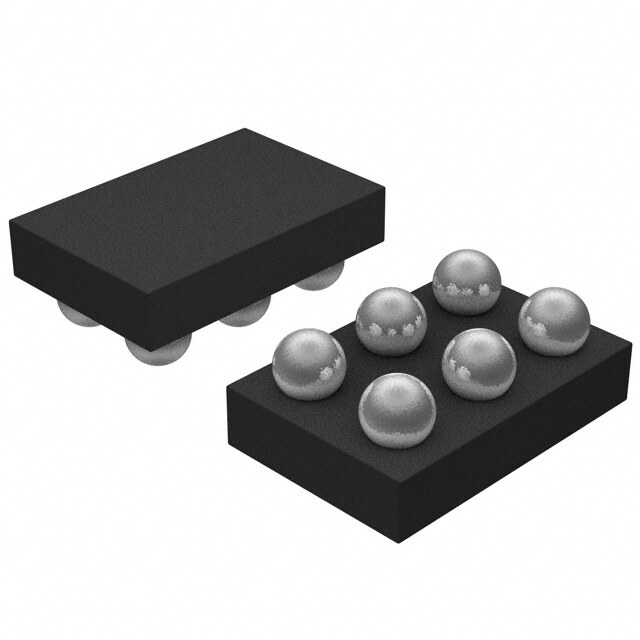
| 产品图片 |
|
| rohs | 符合RoHS无铅 / 符合限制有害物质指令(RoHS)规范要求 |
| 产品系列 | 电源管理 IC,稳压器—开关式稳压器,Texas Instruments TPS60210DGS- |
| 数据手册 | |
| 产品型号 | TPS60210DGS |
| PCN设计/规格 | |
| PWM类型 | - |
| 产品目录页面 | |
| 产品种类 | 稳压器—开关式稳压器 |
| 供应商器件封装 | 10-VSSOP |
| 其它名称 | 296-10959-5 |
| 包装 | 管件 |
| 单位重量 | 18.800 mg |
| 同步整流器 | 无 |
| 商标 | Texas Instruments |
| 安装类型 | 表面贴装 |
| 安装风格 | SMD/SMT |
| 宽度 | 3 mm |
| 封装 | Tube |
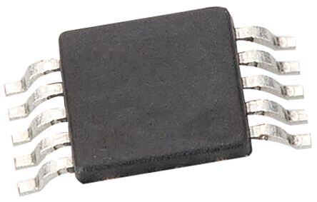
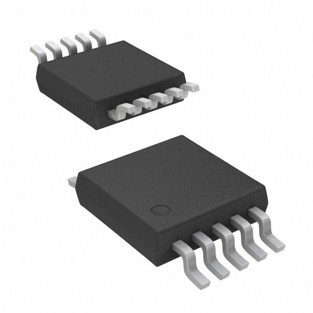
| 封装/外壳 | 10-TFSOP,10-MSOP(0.118",3.00mm 宽) |
| 封装/箱体 | VSSOP-10 |
| 工作温度 | -40°C ~ 85°C |
| 工作温度范围 | - 40 C to + 85 C |
| 工厂包装数量 | 80 |
| 开关频率 | 300 kHz |
| 拓扑结构 | Boost |
| 最大工作温度 | + 85 C |
| 最大输入电压 | 3.6 V |
| 最小工作温度 | - 40 C |
| 最小输入电压 | 1.8 V |
| 标准包装 | 80 |
| 电压-输入 | 1.6 V ~ 3.6 V |
| 电压-输出 | 3.3V |
| 电流-输出 | 100mA |
| 类型 | 升压(升压),切换电容(充电泵) |
| 系列 | TPS60210 |
| 输入电压 | 1.8 V to 3.6 V |
| 输出数 | 1 |
| 输出电压 | 3.3 V |
| 输出电流 | 100 mA |
| 输出端数量 | 1 Output |
| 输出类型 | 固定 |
| 配用 | /product-detail/zh/TPS60210EVM-167/296-10960-ND/381788 |
| 频率-开关 | 300kHz |


- 商务部:美国ITC正式对集成电路等产品启动337调查
- 曝三星4nm工艺存在良率问题 高通将骁龙8 Gen1或转产台积电
- 太阳诱电将投资9.5亿元在常州建新厂生产MLCC 预计2023年完工
- 英特尔发布欧洲新工厂建设计划 深化IDM 2.0 战略
- 台积电先进制程称霸业界 有大客户加持明年业绩稳了
- 达到5530亿美元!SIA预计今年全球半导体销售额将创下新高
- 英特尔拟将自动驾驶子公司Mobileye上市 估值或超500亿美元
- 三星加码芯片和SET,合并消费电子和移动部门,撤换高东真等 CEO
- 三星电子宣布重大人事变动 还合并消费电子和移动部门
- 海关总署:前11个月进口集成电路产品价值2.52万亿元 增长14.8%


PDF Datasheet 数据手册内容提取
(cid:1)(cid:2)(cid:3)(cid:4)(cid:5)(cid:6)(cid:7)(cid:5)(cid:8) (cid:1)(cid:2)(cid:3)(cid:4)(cid:5)(cid:6)(cid:7)(cid:7)(cid:8) (cid:1)(cid:2)(cid:3)(cid:4)(cid:5)(cid:6)(cid:7)(cid:6)(cid:8) (cid:1)(cid:2)(cid:3)(cid:4)(cid:5)(cid:6)(cid:7)(cid:9) (cid:10)(cid:11)(cid:12)(cid:13)(cid:14)(cid:15)(cid:1)(cid:11)(cid:16) (cid:9)(cid:17)(cid:9) (cid:18)(cid:8) (cid:14)(cid:19)(cid:20)(cid:21)(cid:10)(cid:22)(cid:2)(cid:2)(cid:14)(cid:11) (cid:23)(cid:24)(cid:15)(cid:10)(cid:12)(cid:11) (cid:2)(cid:13)(cid:25)(cid:2) (cid:20)(cid:22)(cid:1)(cid:24) (cid:13)(cid:14)(cid:1)(cid:10)(cid:15)(cid:14)(cid:19)(cid:20) (cid:19)(cid:2)(cid:11)(cid:10)(cid:15)(cid:1)(cid:22)(cid:26)(cid:12) (cid:23)(cid:13)(cid:10)(cid:10)(cid:11)(cid:26)(cid:1) SLVS296 − JUNE 2000 (cid:1) features Evaluation Module Available (cid:1) (TPS60210EVM-167) Regulated 3.3-V Output Voltage From a 1.8-V to 3.6-V Input Voltage Range applications (cid:1) UltraLow Operating Current in Snooze (cid:1) Mode, Typical 2 µA Replaces DC/DC Converters With Inductors (cid:1) in Battery-Powered Applications Like: Less Than 5-mV Output Voltage Ripple (PP) − Two Battery Cells to 3.3-V Conversion Achieved With Push-Pull Topology − MSP430 Ultralow-Power Microcontroller (cid:1) Integrated Low-Battery and Power-Good and Other Battery Powered Detector Microprocessor Systems (cid:1) Switching Frequency Can Be Synchronized − Glucose Meters and Other Medical to External Clock Signal Instruments (cid:1) Extends Battery Usage With up to 90% − MP3 Portable Audio Players Efficiency and 35-µA Quiescent Current − Backup-Battery Boost Converters (cid:1) − Cordless Phones, PDAs Easy-To-Design, Low Cost, Low EMI Power Supply Since No Inductors Are Used (cid:1) Compact Converter Solution in UltraSmall 10-Pin MSOP With Only Four External Capacitors Required · description The TPS6021x step-up, regulated charge pumps generate a 3.3-V ±4% output voltage from a 1.8-V to 3.6-V input voltage. These devices are typically powered by two alkaline, NiCd, or NiMH battery cells or by one primary lithium MnO2 (or similar) coin cell and operate down to a minimum supply voltage of 1.6 V. Continuous output current is a minimum of 100 mA for the TPS60210 and TPS60211, and 50 mA for the TPS60212 and TPS60213, all from a 2-V input. TPS60210 INPUT OUTPUT PEAK OUTPUT CURRENT TPS60210 1.6 V to 3.6 V 7 5 3.3 V vs IN OUT INPUT VOLTAGE 2.2CiµF R1 1 LBI R3 C2.o2 µF 350 10 LBO 300 R2 Low Battery Warning 4 C1+ C2+ 6 mA 250 − 1Cµ1F 39 C1− C2− 8 C12µF urrent 200 SNOOZE C ON/OFF GND put 150 2 Out − I O 100 Figure 1. Typical Application Circuit With Low-Battery Warning 50 0 1.6 2.0 2.4 2.8 3.2 3.6 Please be aware that an important notice concerning availability, standard warranVtyI ,− a Inndp uuts Veo ilnta gcrei t−ic aVl applications of TexasInstruments semiconductor products and disclaimers thereto appears at the end of this data sheet. (cid:2)(cid:10)(cid:19)(cid:16)(cid:13)(cid:23)(cid:1)(cid:22)(cid:19)(cid:26) (cid:16)(cid:15)(cid:1)(cid:15) (cid:27)(cid:28)(cid:29)(cid:30)(cid:31)!"#(cid:27)(cid:30)(cid:28) (cid:27)$ %&(cid:31)(cid:31)’(cid:28)# "$ (cid:30)(cid:29) (&)*(cid:27)%"#(cid:27)(cid:30)(cid:28) +"#’(cid:17) Copyright 2000, Texas Instruments Incorporated (cid:2)(cid:31)(cid:30)+&%#$ %(cid:30)(cid:28)(cid:29)(cid:30)(cid:31)! #(cid:30) $(’%(cid:27)(cid:29)(cid:27)%"#(cid:27)(cid:30)(cid:28)$ (’(cid:31) #,’ #’(cid:31)!$ (cid:30)(cid:29) (cid:1)’-"$ (cid:22)(cid:28)$#(cid:31)&!’(cid:28)#$ $#"(cid:28)+"(cid:31)+ ."(cid:31)(cid:31)"(cid:28)#/(cid:17) (cid:2)(cid:31)(cid:30)+&%#(cid:27)(cid:30)(cid:28) ((cid:31)(cid:30)%’$$(cid:27)(cid:28)0 +(cid:30)’$ (cid:28)(cid:30)# (cid:28)’%’$$"(cid:31)(cid:27)*/ (cid:27)(cid:28)%*&+’ #’$#(cid:27)(cid:28)0 (cid:30)(cid:29) "** ("(cid:31)"!’#’(cid:31)$(cid:17) POST OFFICE BOX 655303 • DALLAS, TEXAS 75265 1
(cid:1)(cid:2)(cid:3)(cid:4)(cid:5)(cid:6)(cid:7)(cid:5)(cid:8) (cid:1)(cid:2)(cid:3)(cid:4)(cid:5)(cid:6)(cid:7)(cid:7)(cid:8) (cid:1)(cid:2)(cid:3)(cid:4)(cid:5)(cid:6)(cid:7)(cid:6)(cid:8) (cid:1)(cid:2)(cid:3)(cid:4)(cid:5)(cid:6)(cid:7)(cid:9) (cid:10)(cid:11)(cid:12)(cid:13)(cid:14)(cid:15)(cid:1)(cid:11)(cid:16) (cid:9)(cid:17)(cid:9) (cid:18)(cid:8) (cid:14)(cid:19)(cid:20)(cid:21)(cid:10)(cid:22)(cid:2)(cid:2)(cid:14)(cid:11) (cid:23)(cid:24)(cid:15)(cid:10)(cid:12)(cid:11) (cid:2)(cid:13)(cid:25)(cid:2) (cid:20)(cid:22)(cid:1)(cid:24) (cid:13)(cid:14)(cid:1)(cid:10)(cid:15)(cid:14)(cid:19)(cid:20) (cid:19)(cid:2)(cid:11)(cid:10)(cid:15)(cid:1)(cid:22)(cid:26)(cid:12) (cid:23)(cid:13)(cid:10)(cid:10)(cid:11)(cid:26)(cid:1) SLVS296 − JUNE 2000 description (continued) Three operating modes can be programmed using the SNOOZE pin. When SNOOZE is low, the device is put into snooze mode. In snooze mode, the device operates with a typical quiescent current of 2 µA while the output voltage is maintained at 3.3 V ±6%. This is lower than the self-discharge current of most batteries. Load current in snooze mode is limited to 2 mA. When SNOOZE is high, the device is put into normal operating mode. During normal operating mode, the device operates in the newly developed linskip mode where it switches seamlessly from the power saving pulse-skip mode at light loads to the low-noise constant-frequency linear-regulation mode once the output current exceeds the linskip current threshold of about 7 mA. In this mode, the device operates from the internal oscillator. The device is synchronized to an external clock signal if SNOOZE is clocked; thus switching harmonics can be controlled and minimized. Only four external capacitors are needed to build a complete low-ripple dc/dc converter. The push-pull operating mode of two single-ended charge pumps assures the low output voltage ripple as charge is continuously transferred to the output. All the devices can start with full load current. The devices include a low-battery detector that issues a warning if the battery voltage drops below a user-defined threshold voltage or a power-good detector that goes active when the output voltage reaches about 90% of its nominal value. This dc/dc converter requires no inductors; therefore, EMI of the system is reduced to a minimum, making it easier to use in designs. It is available in the small 10-pin MSOP package (DGS). DGS PACKAGES TPS60210 TPS60211 TPS60212 TPS60213 LBI 1 10 LBO GND 1 10 PG GND 2 9 SNOOZE GND 2 9 SNOOZE C1− 3 8 C2− C1− 3 8 C2− C1+ 4 7 IN C1+ 4 7 IN OUT 5 6 C2+ OUT 5 6 C2+ AVAILABLE OPTIONS MARKING OUTPUT OUTPUT TA PART NUMBER† DGS CURRENT VOLTAGE DEVICE FEATURES PACKAGE (mA) (V) TPS60210DGS AFD 100 3.3 Low-battery detector TPS60211DGS AFE 100 3.3 Power-good detector −−4400°°CC ttoo 8855°°CC TPS60212DGS AFF 50 3.3 Low-battery detector TPS60213DGS AFG 50 3.3 Power-good detector †The DGS package is available taped and reeled. Add R suffix to device type (e.g., TPS60210DGSR) to order quantities of 3000 devices per reel. 2 POST OFFICE BOX 655303 • DALLAS, TEXAS 75265
(cid:1)(cid:2)(cid:3)(cid:4)(cid:5)(cid:6)(cid:7)(cid:5)(cid:8) (cid:1)(cid:2)(cid:3)(cid:4)(cid:5)(cid:6)(cid:7)(cid:7)(cid:8) (cid:1)(cid:2)(cid:3)(cid:4)(cid:5)(cid:6)(cid:7)(cid:6)(cid:8) (cid:1)(cid:2)(cid:3)(cid:4)(cid:5)(cid:6)(cid:7)(cid:9) (cid:10)(cid:11)(cid:12)(cid:13)(cid:14)(cid:15)(cid:1)(cid:11)(cid:16) (cid:9)(cid:17)(cid:9) (cid:18)(cid:8) (cid:14)(cid:19)(cid:20)(cid:21)(cid:10)(cid:22)(cid:2)(cid:2)(cid:14)(cid:11) (cid:23)(cid:24)(cid:15)(cid:10)(cid:12)(cid:11) (cid:2)(cid:13)(cid:25)(cid:2) (cid:20)(cid:22)(cid:1)(cid:24) (cid:13)(cid:14)(cid:1)(cid:10)(cid:15)(cid:14)(cid:19)(cid:20) (cid:19)(cid:2)(cid:11)(cid:10)(cid:15)(cid:1)(cid:22)(cid:26)(cid:12) (cid:23)(cid:13)(cid:10)(cid:10)(cid:11)(cid:26)(cid:1) SLVS296 − JUNE 2000 functional block diagrams TPS60210 and TPS60212 with low-battery detector Charge Pump 1 0° IN Oscillator 180° C1+ C1 C1− SNOOZE Charge Pump 2 Control Circuit C2+ _ C2 C2− + + OUT VREF − Shutdown/ _ Start-Up _ LBI Control + + + − 0.8 x VIN + VREF − GND LBO TPS60211 and TPS60213 with power-good detector 0° Charge Pump 1 IN Oscillator 180° C1+ C1 C1− SNOOZE Charge Pump 2 Control Circuit C2+ _ C2− C2 + + OUT VREF − Shutdown/ _ Start-Up _ Control + + + − 0.8 x VIN + VREF − GND PG POST OFFICE BOX 655303 • DALLAS, TEXAS 75265 3
(cid:1)(cid:2)(cid:3)(cid:4)(cid:5)(cid:6)(cid:7)(cid:5)(cid:8) (cid:1)(cid:2)(cid:3)(cid:4)(cid:5)(cid:6)(cid:7)(cid:7)(cid:8) (cid:1)(cid:2)(cid:3)(cid:4)(cid:5)(cid:6)(cid:7)(cid:6)(cid:8) (cid:1)(cid:2)(cid:3)(cid:4)(cid:5)(cid:6)(cid:7)(cid:9) (cid:10)(cid:11)(cid:12)(cid:13)(cid:14)(cid:15)(cid:1)(cid:11)(cid:16) (cid:9)(cid:17)(cid:9) (cid:18)(cid:8) (cid:14)(cid:19)(cid:20)(cid:21)(cid:10)(cid:22)(cid:2)(cid:2)(cid:14)(cid:11) (cid:23)(cid:24)(cid:15)(cid:10)(cid:12)(cid:11) (cid:2)(cid:13)(cid:25)(cid:2) (cid:20)(cid:22)(cid:1)(cid:24) (cid:13)(cid:14)(cid:1)(cid:10)(cid:15)(cid:14)(cid:19)(cid:20) (cid:19)(cid:2)(cid:11)(cid:10)(cid:15)(cid:1)(cid:22)(cid:26)(cid:12) (cid:23)(cid:13)(cid:10)(cid:10)(cid:11)(cid:26)(cid:1) SLVS296 − JUNE 2000 Terminal Functions TERMINAL II//OO DDEESSCCRRIIPPTTIIOONN NAME NO. C1+ 4 Positive terminal of the flying capacitor C1 C1− 3 Negative terminal of the flying capacitor C1 C2+ 6 Positive terminal of the flying capacitor C2 C2− 8 Negative terminal of the flying capacitor C2 GND 2 Ground IN 7 I Supply input. Bypass IN to GND with a capacitor of a minimum of 2.2 µF. Low-battery detector input for TPS60210 and TPS60212. A low-battery warning is generated at the LBO pin when LBI/GND 1 I the voltage on LBI drops below the threshold of 1.18 V. Connect LBI to GND or VBAT if the low-battery detector function is not used. For the devices TPS60211 and TPS60213, this pin is a ground (GND pin). Open-drain low-battery detector output for TPS60210 and TPS60212. This pin is pulled low if the voltage on LBI drops below the threshold of 1.18 V. A pullup resistor should be connected between LBO and OUT or any other logic supply rail that is lower than 3.6 V. LBO/PG 10 O Open-drain power-good detector output for TPS60211 and TPS60213. As soon as the voltage on OUT reaches about 90% of its nominal value, this pin goes active high. A pullup resistor should be connected between PG and OUT or any other logic supply rail that is lower than 3.6 V. OUT 5 O Regulated 3.3-V power output. Bypass OUT to GND with the output filter capacitor Co. Three operating modes can be programmed with the SNOOZE pin. − SNOOZE = Low programs the device in the snooze mode, enabling ultralow operating current while still maintaining the output voltage to within 3.3 V ±6%. SNOOZE 9 I − SNOOZE = High programs the device into normal operation mode where it runs from the internal oscillator. − If an external clock signal is applied to the SNOOZE pin, the charge pump operates synchronized to the frequency of the external clock signal. detailed description operating principle The TPS6021x charge pumps provide a regulated 3.3-V output from a 1.8-V to 3.6-V input. They deliver a minimum 100-mA load current while maintaining the output at 3.3 V ±4%. Designed specifically for space critical battery-powered applications, the complete converter requires only four external capacitors. The device is using the push-pull topology to achieve the lowest output voltage ripple. The converter is also optimized for a very small board space. It makes use of small-sized capacitors, with the highest output current rating per output capacitance. The TPS6021x circuits consist of an oscillator, a voltage reference, an internal resistive feedback circuit, an error amplifier, two charge-pump power stages with high-current MOSFET switches, a shutdown/start-up circuit, and a control circuit (see functional block diagrams). push-pull operating mode The two single-ended charge-pump power stages operate in the push-pull operating mode (i.e., they operate with a 180°C phase shift). Each single-ended charge pump transfers a charge into its flying capacitor (C1 or C2) in one-half of the period. During the other half of the period (transfer phase), the flying capacitor is placed in series with the input to transfer its charge to the load and output capacitor (C ). While one single-ended charge o pump is in the charge phase, the other one is in the transfer phase. This operation ensures that there is a continuous flow of charge to the load, hence the output capacitor no longer needs to buffer the load current for half of the switching cycle, avoiding the high, inherent output voltage ripple of conventional charge pumps. In order to provide a regulated output voltage of 3.3 V, the TPS6021x devices operate either in constant-frequency linear-regulation control mode or in pulse-skip mode. The mode is automatically selected based on the output current. If the load current is low, the controller switches into the power-saving pulse-skip mode to boost efficiency at low output power. 4 POST OFFICE BOX 655303 • DALLAS, TEXAS 75265
(cid:1)(cid:2)(cid:3)(cid:4)(cid:5)(cid:6)(cid:7)(cid:5)(cid:8) (cid:1)(cid:2)(cid:3)(cid:4)(cid:5)(cid:6)(cid:7)(cid:7)(cid:8) (cid:1)(cid:2)(cid:3)(cid:4)(cid:5)(cid:6)(cid:7)(cid:6)(cid:8) (cid:1)(cid:2)(cid:3)(cid:4)(cid:5)(cid:6)(cid:7)(cid:9) (cid:10)(cid:11)(cid:12)(cid:13)(cid:14)(cid:15)(cid:1)(cid:11)(cid:16) (cid:9)(cid:17)(cid:9) (cid:18)(cid:8) (cid:14)(cid:19)(cid:20)(cid:21)(cid:10)(cid:22)(cid:2)(cid:2)(cid:14)(cid:11) (cid:23)(cid:24)(cid:15)(cid:10)(cid:12)(cid:11) (cid:2)(cid:13)(cid:25)(cid:2) (cid:20)(cid:22)(cid:1)(cid:24) (cid:13)(cid:14)(cid:1)(cid:10)(cid:15)(cid:14)(cid:19)(cid:20) (cid:19)(cid:2)(cid:11)(cid:10)(cid:15)(cid:1)(cid:22)(cid:26)(cid:12) (cid:23)(cid:13)(cid:10)(cid:10)(cid:11)(cid:26)(cid:1) SLVS296 − JUNE 2000 detailed description (continued) constant-frequency mode When the output current is higher than the linskip current threshold, the charge pump runs continuously at the switching frequency f . The control circuit, fed from the error amplifier, controls the charge on C1 and C2 by OSC regulating the r of the integrated MOSFET switches. When the output voltage decreases, the r DS(on) DS(on) decreases as well, resulting in a larger voltage across the flying capacitors C1 and C2. This regulation scheme minimizes output ripple. Since the device switches continuously, the output ripple contains well-defined frequency components, and the circuit requires smaller external capacitors for a given output ripple. However, constant-frequency mode, due to higher operating current, is less efficient at light loads. For this reason, the device switches seamlessly into the pulse-skip mode when the output current drops below the linskip current threshold. pulse-skip mode The device enters the pulse-skip mode when the load current drops below the linskip current threshold of about 7 mA. In pulse-skip mode, the controller disables switching of the power stages when it detects an output voltage higher than 3.3 V. It skips switching cycles until the output voltage drops below 3.3 V. Then the controller reactivates the oscillator and switching of the power stages starts again. A 30-mV output voltage offset is introduced in this mode. The pulse-skip regulation mode minimizes operating current because it does not switch continuously and deactivates all functions except the voltage reference and error amplifier when the output is higher than 3.3 V. Even in pulse-skip mode the r of the MOSFETs is controlled. This way the energy per switching cycle that DS(ON) is transferred by the charge pump from the input to the output is limited to the minimum that is necessary to sustain a regulated output voltage, with the benefit that the output ripple is kept to a minimum. When switching is disabled in pulse-skip mode, the load is isolated from the input. start up, snooze mode, short circuit protection During start-up (i.e., when voltage is applied to the supply pin IN) the input is connected to the output until the output voltage reaches 0.8 x V. When the start-up comparator detects this limit, the actual charge pump output I stages are activated to boost the voltage higher than the input voltage. This precharging of the output current with a limited current ensures a short start-up time and avoids high inrush currents into an empty output capacitor. Driving SNOOZE low, programs the device into the snooze mode. In this mode, the converter will still maintain the output voltage at 3.3 V ±6%. The operating current in snooze mode, is however, drastically reduced to a typical value of 2 µA, while the output current is limited to a maximum of 2 mA. If the load current increases above 2 mA, the controller recognizes a further drop of the output voltage and the device enters the start-up mode to bring the voltage up to its nominal value again. However, it does not switch into the normal operating mode. The device limits short circuit currents to typically 60 mA. synchronization to an external clock signal The operating frequency of the charge pump is limited to 400 kHz in order to avoid troublesome interference problems in the sensitive 455-kHz IF band. The device can either run from the integrated oscillator, or an external clock signal can be used to drive the charge pump. The maximum frequency of the external clock signal is 800 kHz. The switching frequency used internally to drive the charge pump power stages is half of the external clock frequency. The external clock signal is applied to the SNOOZE-pin. The device will switch into the snooze mode if the signal on SNOOZE is held low for more than 10 µs. When the load current drops below the linskip current threshold, the device enters the pulse-skip mode but stays synchronized to the external clock signal. POST OFFICE BOX 655303 • DALLAS, TEXAS 75265 5
(cid:1)(cid:2)(cid:3)(cid:4)(cid:5)(cid:6)(cid:7)(cid:5)(cid:8) (cid:1)(cid:2)(cid:3)(cid:4)(cid:5)(cid:6)(cid:7)(cid:7)(cid:8) (cid:1)(cid:2)(cid:3)(cid:4)(cid:5)(cid:6)(cid:7)(cid:6)(cid:8) (cid:1)(cid:2)(cid:3)(cid:4)(cid:5)(cid:6)(cid:7)(cid:9) (cid:10)(cid:11)(cid:12)(cid:13)(cid:14)(cid:15)(cid:1)(cid:11)(cid:16) (cid:9)(cid:17)(cid:9) (cid:18)(cid:8) (cid:14)(cid:19)(cid:20)(cid:21)(cid:10)(cid:22)(cid:2)(cid:2)(cid:14)(cid:11) (cid:23)(cid:24)(cid:15)(cid:10)(cid:12)(cid:11) (cid:2)(cid:13)(cid:25)(cid:2) (cid:20)(cid:22)(cid:1)(cid:24) (cid:13)(cid:14)(cid:1)(cid:10)(cid:15)(cid:14)(cid:19)(cid:20) (cid:19)(cid:2)(cid:11)(cid:10)(cid:15)(cid:1)(cid:22)(cid:26)(cid:12) (cid:23)(cid:13)(cid:10)(cid:10)(cid:11)(cid:26)(cid:1) SLVS296 − JUNE 2000 detailed description (continued) low-battery detector (TPS60210 and TPS60212) The low-battery comparator trips at 1.18 V ±5% when the voltage on pin LBI ramps down. The voltage V (TRIP) at which the low-battery warning is issued can be adjusted with a resistive divider as shown in Figure 2. The sum of resistors R1 and R2 is recommended to be in the 100-kΩ to 1-MΩ range. LBO is an open drain output. An external pullup resistor to OUT, or any other voltage rail in the appropriate range, in the 100-kΩ to 1-MΩ range is recommended. During start-up, the LBO output signal is invalid for the first 500µs. LBO is high impedance when the device is programmed into snooze mode. If the low battery function is not used, connect LBI to ground and leave LBO unconnected. When the device is programmed into snooze mode (SNOOZE = LOW), the low-battery detector is disabled. VO IN VBAT R3 R1 (cid:2) (cid:4) LBO _ LBI V(TRIP)(cid:1)1.18V 1(cid:3)RR12 + R2 + VREF − Figure 2. Programming of the Low-Battery Comparator Trip Voltage A 100-nF ceramic capacitor should be connected in parallel to R2 if large line transients are expected. These voltage drops may inadvertently trigger the low-battery comparator and produce a wrong low-battery warning signal at the LBO pin. Formulas to calculate the resistive divider for low-battery detection, with V = 1.13 V to 1.23 V and the sum LBI of resistors R1 and R2 equal 1 MΩ: V R2(cid:1)1M(cid:1)(cid:5) LBI (1) V Bat R1(cid:1)1M(cid:1)(cid:6)R2 (2) Formulas to calculate the minimum and maximum battery voltage: R1 (cid:3)R2 (min) (max) V (cid:1)V (cid:5) (3) Bat(min) LBI(min) R2 (max) R1 (cid:3)R2 (max) (min) V (cid:1)V (cid:5) (4) Bat(max) LBI(max) R2 (min) 6 POST OFFICE BOX 655303 • DALLAS, TEXAS 75265
(cid:1)(cid:2)(cid:3)(cid:4)(cid:5)(cid:6)(cid:7)(cid:5)(cid:8) (cid:1)(cid:2)(cid:3)(cid:4)(cid:5)(cid:6)(cid:7)(cid:7)(cid:8) (cid:1)(cid:2)(cid:3)(cid:4)(cid:5)(cid:6)(cid:7)(cid:6)(cid:8) (cid:1)(cid:2)(cid:3)(cid:4)(cid:5)(cid:6)(cid:7)(cid:9) (cid:10)(cid:11)(cid:12)(cid:13)(cid:14)(cid:15)(cid:1)(cid:11)(cid:16) (cid:9)(cid:17)(cid:9) (cid:18)(cid:8) (cid:14)(cid:19)(cid:20)(cid:21)(cid:10)(cid:22)(cid:2)(cid:2)(cid:14)(cid:11) (cid:23)(cid:24)(cid:15)(cid:10)(cid:12)(cid:11) (cid:2)(cid:13)(cid:25)(cid:2) (cid:20)(cid:22)(cid:1)(cid:24) (cid:13)(cid:14)(cid:1)(cid:10)(cid:15)(cid:14)(cid:19)(cid:20) (cid:19)(cid:2)(cid:11)(cid:10)(cid:15)(cid:1)(cid:22)(cid:26)(cid:12) (cid:23)(cid:13)(cid:10)(cid:10)(cid:11)(cid:26)(cid:1) SLVS296 − JUNE 2000 detailed description (continued) Table 1. Recommended Values for the Resistive Divider From the E96 Series (±1%) VIN/V R1/kΩ R2/kΩ VTRIP(MIN)/V VTRIP(MAX)/V 1.6 267 750 1.524 1.677 1.7 301 681 1.620 1.785 1.8 340 649 1.710 1.887 1.9 374 619 1.799 1.988 2.0 402 576 1.903 2.106 power-good detector (TPS60211 and TPS60213) The power-good output is an open-drain output that pulls low when the output is out of regulation. When the output rises above 91% of its nominal voltage, the power-good output is released. When the device is programmed into snooze mode (SNOOZE = LOW), the power-good detector is disabled and PG is high impedance. In normal operation, an external pullup resistor must be connected between PG and OUT, or any other voltage rail in the appropriate range. The pullup resistor should be in the 100-kΩ to 1-MΩ range. If the PG output is not used, it should remain unconnected. absolute maximum ratings over operating free-air temperature range (unless otherwise noted)† Voltage range: IN, OUT, SNOOZE, LBI, LBO, PG to GND . . . . . . . . . . . . . . . . . . . . . . . . . . . . −0.3 V to 3.6 V C1+, C2+ to GND . . . . . . . . . . . . . . . . . . . . . . . . . . . . . . . . . . . . . . . . . . −0.3 V to (V + 0.3 V) O C1−, C2− to GND . . . . . . . . . . . . . . . . . . . . . . . . . . . . . . . . . . . . . . . . . . . . −0.3 V to (V + 0.3 V) I Continuous total power dissipation . . . . . . . . . . . . . . . . . . . . . . . . . . . . . . . . . . . . . . See Dissipation Rating Table Continuous output current: TPS60210, TPS60211 . . . . . . . . . . . . . . . . . . . . . . . . . . . . . . . . . . . . . . . . . . 150 mA TPS60212, TPS60213 . . . . . . . . . . . . . . . . . . . . . . . . . . . . . . . . . . . . . . . . . . . 75 mA Storage temperature range, T . . . . . . . . . . . . . . . . . . . . . . . . . . . . . . . . . . . . . . . . . . . . . . . . . . . . −55°C to 150°C stg Maximum junction temperature, T . . . . . . . . . . . . . . . . . . . . . . . . . . . . . . . . . . . . . . . . . . . . . . . . . . . . . . . . . 150°C J †Stresses beyond those listed under “absolute maximum ratings” may cause permanent damage to the device. These are stress ratings only, and functional operation of the device at these or any other conditions beyond those indicated under “recommended operating conditions” is not implied. Exposure to absolute-maximum-rated conditions for extended periods may affect device reliability. DISSIPATION RATING TABLE 1 FREE-AIR TEMPERATURE TA ≤ 25°C DERATING FACTOR TA = 70°C TA = 85°C PACKAGE POWER RATING ABOVE TA = 25°C POWER RATING POWER RATING DGS 424 mW 3.4 mW/(cid:2)C 178 mW 136 mW The thermal resistance junction to ambient of the DGS package is RTH−JA = 294°C/W. recommended operating conditions MIN NOM MAX UNIT Input voltage range, VI 1.6 3.6 V Input capacitor, Ci 2.2 µF Flying capacitors, C1, C2 1 µF Output capacitor, Co 2.2 µF Operating junction temperature, TJ −40 125 °C POST OFFICE BOX 655303 • DALLAS, TEXAS 75265 7
(cid:1)(cid:2)(cid:3)(cid:4)(cid:5)(cid:6)(cid:7)(cid:5)(cid:8) (cid:1)(cid:2)(cid:3)(cid:4)(cid:5)(cid:6)(cid:7)(cid:7)(cid:8) (cid:1)(cid:2)(cid:3)(cid:4)(cid:5)(cid:6)(cid:7)(cid:6)(cid:8) (cid:1)(cid:2)(cid:3)(cid:4)(cid:5)(cid:6)(cid:7)(cid:9) (cid:10)(cid:11)(cid:12)(cid:13)(cid:14)(cid:15)(cid:1)(cid:11)(cid:16) (cid:9)(cid:17)(cid:9) (cid:18)(cid:8) (cid:14)(cid:19)(cid:20)(cid:21)(cid:10)(cid:22)(cid:2)(cid:2)(cid:14)(cid:11) (cid:23)(cid:24)(cid:15)(cid:10)(cid:12)(cid:11) (cid:2)(cid:13)(cid:25)(cid:2) (cid:20)(cid:22)(cid:1)(cid:24) (cid:13)(cid:14)(cid:1)(cid:10)(cid:15)(cid:14)(cid:19)(cid:20) (cid:19)(cid:2)(cid:11)(cid:10)(cid:15)(cid:1)(cid:22)(cid:26)(cid:12) (cid:23)(cid:13)(cid:10)(cid:10)(cid:11)(cid:26)(cid:1) SLVS296 − JUNE 2000 electrical characteristics at C= 2.2 µF, C1 = C2 = 1 µF, C = 2.2 µF, T = −40°C to 85°C, V = 2.4 V, i o A I SNOOZE = V (unless otherwise noted) I PARAMETER TEST CONDITIONS MIN TYP MAX UNIT TPS60210 and TPS60211, VI = 2 V 100 mA IIOO((MMAAXX)) MMaaxxiimmuumm ccoonnttiinnuuoouuss oouuttppuutt ccuurrrreenntt TPS60212 and TPS60213, VI = 2 V 50 mA 1.6 V < VI < 1.8 V, 0 < IO < 0.25 × IO(MAX) 3 V 1.8 V < VI < 2 V, 0 < IO < 0.5 × IO(MAX) 3.17 3.3 3.43 V OOuuttppuutt vvoollttaaggee 2 V < VI < 3.3 V, 0 < IO < IO(MAX) 3.17 3.3 3.43 V VVOO 3.3 V < VI < 3.6 V, 0 < IO < IO(MAX) 3.17 3.3 3.47 V SNOOZE = GND, 1.8 V < VI < 3.6 V, Output voltage in snooze mode 3.1 3.3 3.47 V IO < 2 mA VPP Output voltage ripple IO = IO(MAX) 5 mVPP Quiescent current (no-load input current) IO = 0 mA, VI = 1.8 V to 3.6 V 35 70 µA II((QQ)) Quiescent current in snooze mode SNOOZE = GND, IO = 0 mA 2 5 µA f(OSC) Internal switching frequency 200 300 400 kHz f(SYNC) External clock signal frequency 400 600 800 kHz External clock signal duty cycle 30% 70% VIL SNOOZE input low voltage VI = 1.6 V to 3.6 V 0.3 × VI V VIH SNOOZE input high voltage VI = 1.6 V to 3.6 V 0.7 × VI V Ilkg SNOOZE input leakage current SNOOZE = GND or VI 0.01 0.1 µA LinSkip current threshold VI = 2 V to 3 V 7 mA VI = 2.4 V, 1 mA < IO < IO(MAX), 0.015 TC = 25°C OOuuttppuutt llooaadd rreegguullaattiioonn %%//mmAA VI = 2.4 V, 10 mA < IO < IO(MAX), 0.008 TC = 25°C 2 V < VI < 3.3 V, IO = 0.5 x IO(MAX), Output line regulation 0.28 %V TA = 25°C I(SC) Short circuit current VI = 2.4 V, VO = 0 V 60 mA electrical characteristics for low-battery comparator of devices TPS60210 and TPS60212 at T = −40°C to 85°C, V = 2.4 V and SNOOZE = V (unless otherwise noted) A I I PARAMETER TEST CONDITIONS MIN TYP MAX UNIT V(LBI) LBI trip voltage VI = 1.6 V to 2.2 V, Tc = 0°C to 70°C 1.13 1.18 1.23 V LBI trip voltage hysteresis For rising voltage at LBI 10 mV II(LBI) LBI input current V(LBI) = 1.3 V 20 100 nA VO(LBO) LBO output voltage low V(LBI) = 0 V, I(LBO) = 1 mA 0.4 V Ilkg(LBO) LBO leakage current V(LBI) = 1.3 V, V(LBO) = 3.3 V 0.01 0.1 µA NOTE: During start-up of the converter the LBO output signal is invalid for the first 500 µs. electrical characteristics for power-good comparator of devices TPS60211 and TPS60213 at T = −40°C to 85°C, V = 2.4 V and SNOOZE = V (unless otherwise noted) A I I PARAMETER TEST CONDITIONS MIN TYP MAX UNIT V(PG) Power-good trip voltage Tc = 0°C to 70°C 0.87 × VO 0.91 × VO 0.95 × VO V Vhys(PG) Power-good trip voltage hysteresis VO decreasing, Tc = 0°C to 70°C 1% VO(PG) Power-good output voltage low VO = 0 V, I(PG) = 1 mA 0.4 V Ilkg(PG) Power-good leakage current VO = 3.3 V, V(PG) = 3.3 V 0.01 0.1 µA NOTE: During start-up of the converter the PG output signal is invalid for the first 500 µs. 8 POST OFFICE BOX 655303 • DALLAS, TEXAS 75265
(cid:1)(cid:2)(cid:3)(cid:4)(cid:5)(cid:6)(cid:7)(cid:5)(cid:8) (cid:1)(cid:2)(cid:3)(cid:4)(cid:5)(cid:6)(cid:7)(cid:7)(cid:8) (cid:1)(cid:2)(cid:3)(cid:4)(cid:5)(cid:6)(cid:7)(cid:6)(cid:8) (cid:1)(cid:2)(cid:3)(cid:4)(cid:5)(cid:6)(cid:7)(cid:9) (cid:10)(cid:11)(cid:12)(cid:13)(cid:14)(cid:15)(cid:1)(cid:11)(cid:16) (cid:9)(cid:17)(cid:9) (cid:18)(cid:8) (cid:14)(cid:19)(cid:20)(cid:21)(cid:10)(cid:22)(cid:2)(cid:2)(cid:14)(cid:11) (cid:23)(cid:24)(cid:15)(cid:10)(cid:12)(cid:11) (cid:2)(cid:13)(cid:25)(cid:2) (cid:20)(cid:22)(cid:1)(cid:24) (cid:13)(cid:14)(cid:1)(cid:10)(cid:15)(cid:14)(cid:19)(cid:20) (cid:19)(cid:2)(cid:11)(cid:10)(cid:15)(cid:1)(cid:22)(cid:26)(cid:12) (cid:23)(cid:13)(cid:10)(cid:10)(cid:11)(cid:26)(cid:1) SLVS296 − JUNE 2000 TYPICAL CHARACTERISTICS Table of Graphs FIGURES vs Output current (TPS60210 and TPS60212) 3, 4 η EEffffiicciieennccyy vs Input voltage 5 IO Output current vs Input voltage 6 vs Output current (TPS60210 and TPS60212) 7, 8 VVOO OOuuttppuutt vvoollttaaggee vs Input voltage (TPS60210 and TPS60212) 9, 10 vs Input voltage 11 IIQQ QQuuiieesscceenntt ssuuppppllyy ccuurrrreenntt vs Output current in snooze mode 12 VO Output voltage vs Time (Exit from snooze mode) 13 vs Time 14, 15, 16 VVOO OOuuttppuutt vvoollttaaggee rriippppllee vs Time in snooze mode 17, 18 Load transient response 19 Line transient response 20 NOTE: All typical characteristics were measured using the typical application circuit of Figure 21 (unless otherwise noted). TPS60210 TPS60212 EFFICIENCY EFFICIENCY vs vs OUTPUT CURRENT OUTPUT CURRENT 100 100 90 90 80 80 70 70 % % − 60 − 60 cy VI = 1.8 V cy n 50 n 50 e e ci VI = 2.4 V ci VI = 1.8 V Effi 40 Effi 40 30 VI = 2.7 V 30 VI = 2.4 V 20 20 VI = 2.7 V 10 10 0 0 0.1 1 10 100 1000 0.1 1 10 100 IO − Output Current − mA IO − Output Current − mA Figure 3 Figure 4 POST OFFICE BOX 655303 • DALLAS, TEXAS 75265 9
(cid:1)(cid:2)(cid:3)(cid:4)(cid:5)(cid:6)(cid:7)(cid:5)(cid:8) (cid:1)(cid:2)(cid:3)(cid:4)(cid:5)(cid:6)(cid:7)(cid:7)(cid:8) (cid:1)(cid:2)(cid:3)(cid:4)(cid:5)(cid:6)(cid:7)(cid:6)(cid:8) (cid:1)(cid:2)(cid:3)(cid:4)(cid:5)(cid:6)(cid:7)(cid:9) (cid:10)(cid:11)(cid:12)(cid:13)(cid:14)(cid:15)(cid:1)(cid:11)(cid:16) (cid:9)(cid:17)(cid:9) (cid:18)(cid:8) (cid:14)(cid:19)(cid:20)(cid:21)(cid:10)(cid:22)(cid:2)(cid:2)(cid:14)(cid:11) (cid:23)(cid:24)(cid:15)(cid:10)(cid:12)(cid:11) (cid:2)(cid:13)(cid:25)(cid:2) (cid:20)(cid:22)(cid:1)(cid:24) (cid:13)(cid:14)(cid:1)(cid:10)(cid:15)(cid:14)(cid:19)(cid:20) (cid:19)(cid:2)(cid:11)(cid:10)(cid:15)(cid:1)(cid:22)(cid:26)(cid:12) (cid:23)(cid:13)(cid:10)(cid:10)(cid:11)(cid:26)(cid:1) SLVS296 − JUNE 2000 TYPICAL CHARACTERISTICS TPS60210 TPS60210 EFFICIENCY PEAK OUTPUT CURRENT vs vs INPUT VOLTAGE INPUT VOLTAGE 100 350 90 300 80 A m 250 70 − − % 60 rent 200 y ur cienc 50 IO = 50 mA put C 150 Effi 40 Out 30 I − O 100 20 50 10 0 0 1.6 2.0 2.4 2.8 3.2 3.6 1.6 2.0 2.4 2.8 3.2 3.6 VI − Input Voltage − V VI − Input Voltage − V Figure 5 Figure 6 TPS60210 TPS60212 OUTPUT VOLTAGE OUTPUT VOLTAGE vs vs OUTPUT CURRENT OUTPUT CURRENT 3.5 3.35 VI = 2.7 V VI = 3.6 V 3.30 3.4 VI = 3.6 V 3.25 V V − 3.3 − VI = 1.8 V VI = 2.4 V e e ag ag 3.20 Volt 3.2 VI = 1.8 V Volt ut ut 3.15 p p ut VI = 2.7 V ut O 3.1 O − O − O 3.10 V VI = 2.4 V V 3.0 3.05 2.9 3 1 10 100 1000 1 10 100 IO − Output Current − mA IO − Output Current − mA Figure 7 Figure 8 10 POST OFFICE BOX 655303 • DALLAS, TEXAS 75265
(cid:1)(cid:2)(cid:3)(cid:4)(cid:5)(cid:6)(cid:7)(cid:5)(cid:8) (cid:1)(cid:2)(cid:3)(cid:4)(cid:5)(cid:6)(cid:7)(cid:7)(cid:8) (cid:1)(cid:2)(cid:3)(cid:4)(cid:5)(cid:6)(cid:7)(cid:6)(cid:8) (cid:1)(cid:2)(cid:3)(cid:4)(cid:5)(cid:6)(cid:7)(cid:9) (cid:10)(cid:11)(cid:12)(cid:13)(cid:14)(cid:15)(cid:1)(cid:11)(cid:16) (cid:9)(cid:17)(cid:9) (cid:18)(cid:8) (cid:14)(cid:19)(cid:20)(cid:21)(cid:10)(cid:22)(cid:2)(cid:2)(cid:14)(cid:11) (cid:23)(cid:24)(cid:15)(cid:10)(cid:12)(cid:11) (cid:2)(cid:13)(cid:25)(cid:2) (cid:20)(cid:22)(cid:1)(cid:24) (cid:13)(cid:14)(cid:1)(cid:10)(cid:15)(cid:14)(cid:19)(cid:20) (cid:19)(cid:2)(cid:11)(cid:10)(cid:15)(cid:1)(cid:22)(cid:26)(cid:12) (cid:23)(cid:13)(cid:10)(cid:10)(cid:11)(cid:26)(cid:1) SLVS296 − JUNE 2000 TYPICAL CHARACTERISTICS TPS60210 TPS60212 OUTPUT VOLTAGE OUTPUT VOLTAGE vs vs INPUT VOLTAGE INPUT VOLTAGE 3.4 3.35 3.3 3.30 V 1 mA ge − 3.2 − V 3.25 1 mA a e − Output Volt 33..01 100 mA 50 mA Output Voltag 33..1250 50 mA 25 mA VO − 2.9 VO 3.10 2.8 3.05 2.7 3.00 1.6 2.0 2.4 2.8 3.2 3.6 1.6 2.0 2.4 2.8 3.2 3.6 VI − Input Voltage − V VI − Input Voltage − V Figure 9 Figure 10 QUIESCENT SUPPLY CURRENT QUIESCENT SUPPLY CURRENT vs vs INPUT VOLTAGE OUTPUT CURRENT IN SNOOZE MODE 40 70 38 IO = 0 mA VI = 2.4 V SNOOZE = GND SNOOZE = VI 60 36 A A µCurrent − 3342 µCurrent − 4500 Quiescent 3208 Quiescent 30 I − Q 26 I − Q 20 24 10 22 20 0 1.6 1.8 2.0 2.2 2.4 2.6 2.8 3.0 3.2 3.4 3.6 0 0.2 0.4 0.6 0.8 1 1.2 1.4 1.6 1.8 2 VI − Input Voltage − V IO − Output Current − mA Figure 11 Figure 12 POST OFFICE BOX 655303 • DALLAS, TEXAS 75265 11
(cid:1)(cid:2)(cid:3)(cid:4)(cid:5)(cid:6)(cid:7)(cid:5)(cid:8) (cid:1)(cid:2)(cid:3)(cid:4)(cid:5)(cid:6)(cid:7)(cid:7)(cid:8) (cid:1)(cid:2)(cid:3)(cid:4)(cid:5)(cid:6)(cid:7)(cid:6)(cid:8) (cid:1)(cid:2)(cid:3)(cid:4)(cid:5)(cid:6)(cid:7)(cid:9) (cid:10)(cid:11)(cid:12)(cid:13)(cid:14)(cid:15)(cid:1)(cid:11)(cid:16) (cid:9)(cid:17)(cid:9) (cid:18)(cid:8) (cid:14)(cid:19)(cid:20)(cid:21)(cid:10)(cid:22)(cid:2)(cid:2)(cid:14)(cid:11) (cid:23)(cid:24)(cid:15)(cid:10)(cid:12)(cid:11) (cid:2)(cid:13)(cid:25)(cid:2) (cid:20)(cid:22)(cid:1)(cid:24) (cid:13)(cid:14)(cid:1)(cid:10)(cid:15)(cid:14)(cid:19)(cid:20) (cid:19)(cid:2)(cid:11)(cid:10)(cid:15)(cid:1)(cid:22)(cid:26)(cid:12) (cid:23)(cid:13)(cid:10)(cid:10)(cid:11)(cid:26)(cid:1) SLVS296 − JUNE 2000 TYPICAL CHARACTERISTICS TPS60210 TPS60210 OUTPUT VOLTAGE OUTPUT VOLTAGE RIPPLE vs vs TIME TIME 3.6 V 3.38 − oltage 3.5 3.36 VIOI == 21. 4m VA V ut 3.4 3.34 p Out − V − 3.3 ge 3.32 O a V 3.2 Volt 3.30 ut p ut 3.28 O ZE − O O O V 3.26 N S High 3.24 Low 3.22 0 50 100 150 200 250 300 350 400 450 500 0 5 10 15 20 25 30 35 40 45 50 t − Time − ms t − Time − µs Figure 13 Figure 14 TPS60210 TPS60210 OUTPUT VOLTAGE RIPPLE OUTPUT VOLTAGE RIPPLE vs vs TIME TIME 3.38 3.38 VI = 2.4 V VI = 2.4 V 3.36 IO = 10 mA 3.36 IO = 100 mA 3.34 3.34 V V ge − 3.32 ge − 3.32 Volta 3.30 Volta 3.30 ut ut p p Out 3.28 Out 3.28 − − O O V 3.26 V 3.26 3.24 3.24 3.22 3.22 0 1 2 3 4 5 6 7 8 9 10 0 1 2 3 4 5 6 7 8 9 10 t − Time − µs t − Time − µs Figure 15 Figure 16 12 POST OFFICE BOX 655303 • DALLAS, TEXAS 75265
(cid:1)(cid:2)(cid:3)(cid:4)(cid:5)(cid:6)(cid:7)(cid:5)(cid:8) (cid:1)(cid:2)(cid:3)(cid:4)(cid:5)(cid:6)(cid:7)(cid:7)(cid:8) (cid:1)(cid:2)(cid:3)(cid:4)(cid:5)(cid:6)(cid:7)(cid:6)(cid:8) (cid:1)(cid:2)(cid:3)(cid:4)(cid:5)(cid:6)(cid:7)(cid:9) (cid:10)(cid:11)(cid:12)(cid:13)(cid:14)(cid:15)(cid:1)(cid:11)(cid:16) (cid:9)(cid:17)(cid:9) (cid:18)(cid:8) (cid:14)(cid:19)(cid:20)(cid:21)(cid:10)(cid:22)(cid:2)(cid:2)(cid:14)(cid:11) (cid:23)(cid:24)(cid:15)(cid:10)(cid:12)(cid:11) (cid:2)(cid:13)(cid:25)(cid:2) (cid:20)(cid:22)(cid:1)(cid:24) (cid:13)(cid:14)(cid:1)(cid:10)(cid:15)(cid:14)(cid:19)(cid:20) (cid:19)(cid:2)(cid:11)(cid:10)(cid:15)(cid:1)(cid:22)(cid:26)(cid:12) (cid:23)(cid:13)(cid:10)(cid:10)(cid:11)(cid:26)(cid:1) SLVS296 − JUNE 2000 TYPICAL CHARACTERISTICS TPS60210 TPS60210 OUTPUT VOLTAGE RIPPLE IN SNOOZE MODE OUTPUT VOLTAGE RIPPLE IN SNOOZE MODE vs vs TIME TIME 3.7 3.7 VI = 2.4 V VI = 2.4 V 3.6 ICOO = = 1 1 m0 AµF (Tantalum) 3.6 ICOO = = 1 2 m.2A µF (Ceramic) SNOOZE = Low SNOOZE = Low 3.5 3.5 V V − − ge 3.4 ge 3.4 Volta Volta ut 3.3 ut 3.3 p p ut ut O 3.2 O 3.2 − − O O V 3.1 V 3.1 3 3 2.9 2.9 0 100 200 300 400 500 600 700 800 900 1000 0 100 200 300 400 500 600 700 800 900 1000 t − Time − µs t − Time − µs Figure 17 Figure 18 TPS60210 TPS60210 LOAD TRANSIENT RESPONSE LINE TRANSIENT RESPONSE V ge − VI = 2.4 V e − V IO = 50 mA a 3.30 g Volt olta put 3.28 ut V 3.32 Out utp O − 3.26 − 3.30 O V O V 3.24 3.28 A m nt − e − V 3.26 e g utput Curr100 mA nput Volta 2.8 V − OO10 mA V− II2.2 V I 0 50 100 150 200 250 300 350 400 450 500 0 1 2 3 4 5 6 7 8 9 10 t − Time − µs t − Time − ms Figure 19 Figure 20 POST OFFICE BOX 655303 • DALLAS, TEXAS 75265 13
(cid:1)(cid:2)(cid:3)(cid:4)(cid:5)(cid:6)(cid:7)(cid:5)(cid:8) (cid:1)(cid:2)(cid:3)(cid:4)(cid:5)(cid:6)(cid:7)(cid:7)(cid:8) (cid:1)(cid:2)(cid:3)(cid:4)(cid:5)(cid:6)(cid:7)(cid:6)(cid:8) (cid:1)(cid:2)(cid:3)(cid:4)(cid:5)(cid:6)(cid:7)(cid:9) (cid:10)(cid:11)(cid:12)(cid:13)(cid:14)(cid:15)(cid:1)(cid:11)(cid:16) (cid:9)(cid:17)(cid:9) (cid:18)(cid:8) (cid:14)(cid:19)(cid:20)(cid:21)(cid:10)(cid:22)(cid:2)(cid:2)(cid:14)(cid:11) (cid:23)(cid:24)(cid:15)(cid:10)(cid:12)(cid:11) (cid:2)(cid:13)(cid:25)(cid:2) (cid:20)(cid:22)(cid:1)(cid:24) (cid:13)(cid:14)(cid:1)(cid:10)(cid:15)(cid:14)(cid:19)(cid:20) (cid:19)(cid:2)(cid:11)(cid:10)(cid:15)(cid:1)(cid:22)(cid:26)(cid:12) (cid:23)(cid:13)(cid:10)(cid:10)(cid:11)(cid:26)(cid:1) SLVS296 − JUNE 2000 APPLICATION INFORMATION capacitor selection The TPS6021x devices require only four external capacitors to achieve a very low output voltage ripple. The capacitor values are closely linked to the required output current. Low ESR (< 0.1-Ω) capacitors should be used at the input and output of the charge pump. In general, the transfer capacitors (C1 and C2) will be the smallest. A 1-µF value is recommended if full load current performance is needed. With smaller capacitor values, the maximum possible load current is reduced and the linskip threshold is lowered. The input capacitor improves system efficiency by reducing the input impedance. It also stabilizes the input current of the power source. The input capacitor should be chosen according to the power supply used, the distance from the power source to the converter IC. C is recommended to be about two to four times as large I as the flying capacitors C1 and C2. The minimum required capacitance is 2.2 µF. Larger values will improve the load transient performance and will reduce the maximum output ripple voltage. The larger the output capacitor, the better the output voltage accuracy, and the more output current can be drawn from the converter when programmed into snooze mode. Only ceramic capacitors are recommended for input, output and flying capacitors. Depending on the material used to manufacture them, ceramic capacitors might lose their capacitance over temperature and voltage. Ceramic capacitors of type X7R or X5R material will keep their capacitance over temperature and voltage, whereas Z5U- or Y5V-type capacitors will decrease in capacitance. Table 1 lists recommended capacitor values. 14 POST OFFICE BOX 655303 • DALLAS, TEXAS 75265
(cid:1)(cid:2)(cid:3)(cid:4)(cid:5)(cid:6)(cid:7)(cid:5)(cid:8) (cid:1)(cid:2)(cid:3)(cid:4)(cid:5)(cid:6)(cid:7)(cid:7)(cid:8) (cid:1)(cid:2)(cid:3)(cid:4)(cid:5)(cid:6)(cid:7)(cid:6)(cid:8) (cid:1)(cid:2)(cid:3)(cid:4)(cid:5)(cid:6)(cid:7)(cid:9) (cid:10)(cid:11)(cid:12)(cid:13)(cid:14)(cid:15)(cid:1)(cid:11)(cid:16) (cid:9)(cid:17)(cid:9) (cid:18)(cid:8) (cid:14)(cid:19)(cid:20)(cid:21)(cid:10)(cid:22)(cid:2)(cid:2)(cid:14)(cid:11) (cid:23)(cid:24)(cid:15)(cid:10)(cid:12)(cid:11) (cid:2)(cid:13)(cid:25)(cid:2) (cid:20)(cid:22)(cid:1)(cid:24) (cid:13)(cid:14)(cid:1)(cid:10)(cid:15)(cid:14)(cid:19)(cid:20) (cid:19)(cid:2)(cid:11)(cid:10)(cid:15)(cid:1)(cid:22)(cid:26)(cid:12) (cid:23)(cid:13)(cid:10)(cid:10)(cid:11)(cid:26)(cid:1) SLVS296 − JUNE 2000 APPLICATION INFORMATION Table 2. Recommended Capacitor Values (Ceramic X5R and X7R) FLYING INPUT OUTPUT OUTPUT VOLTAGE OUTPUT VOLTAGE LOAD CURRENT, CAPACITORS, CAPACITOR, CAPACITOR, RIPPLE IN LINEAR MODE, RIPPLE IN SKIP MODE, ILOAD (mA) C1/C2 CIN COUT VP-P VP-P (µF) (µF) (µF) (mV) (mV) 0−100 1 2.2 2.2 3 20 0−100 1 4.7 4.7 3 10 0−100 1 2.2 10 3 7 0−100 2.2 4.7 4.7 3 10 0−50 0.47 2.2 2.2 3 20 0−25 0.22 2.2 2.2 5 15 0−10 0.1 2.2 2.2 5 15 Table 3. Recommended Capacitor Types MANUFACTURER PART NUMBER SIZE CAPACITANCE TYPE TTaaiiyyoo YYuuddeenn UMK212BJ104MG 0805 0.1 µF Ceramic EMK212BJ224MG 0805 0.22 µF Ceramic EMK212BJ474MG 0805 0.47 µF Ceramic LMK212BJ105KG 0805 1 µF Ceramic LMK212BJ225MG 0805 2.2 µF Ceramic EMK316BJ225KL 1206 2.2 µF Ceramic LMK316BJ475KL 1206 4.7 µF Ceramic JMK316BJ106ML 1206 10 µF Ceramic AAVVXX 0805ZC105KAT2A 0805 1 µF Ceramic 1206ZC225KAT2A 1206 2.2 µF Ceramic Table 4. Recommended Capacitor Manufacturers MANUFACTURER CAPACITOR TYPE INTERNET SITE Taiyo Yuden X7R/X5R ceramic http://www.t−yuden.com/ AVX X7R/X5R ceramic http://www.avxcorp.com/ POST OFFICE BOX 655303 • DALLAS, TEXAS 75265 15
(cid:1)(cid:2)(cid:3)(cid:4)(cid:5)(cid:6)(cid:7)(cid:5)(cid:8) (cid:1)(cid:2)(cid:3)(cid:4)(cid:5)(cid:6)(cid:7)(cid:7)(cid:8) (cid:1)(cid:2)(cid:3)(cid:4)(cid:5)(cid:6)(cid:7)(cid:6)(cid:8) (cid:1)(cid:2)(cid:3)(cid:4)(cid:5)(cid:6)(cid:7)(cid:9) (cid:10)(cid:11)(cid:12)(cid:13)(cid:14)(cid:15)(cid:1)(cid:11)(cid:16) (cid:9)(cid:17)(cid:9) (cid:18)(cid:8) (cid:14)(cid:19)(cid:20)(cid:21)(cid:10)(cid:22)(cid:2)(cid:2)(cid:14)(cid:11) (cid:23)(cid:24)(cid:15)(cid:10)(cid:12)(cid:11) (cid:2)(cid:13)(cid:25)(cid:2) (cid:20)(cid:22)(cid:1)(cid:24) (cid:13)(cid:14)(cid:1)(cid:10)(cid:15)(cid:14)(cid:19)(cid:20) (cid:19)(cid:2)(cid:11)(cid:10)(cid:15)(cid:1)(cid:22)(cid:26)(cid:12) (cid:23)(cid:13)(cid:10)(cid:10)(cid:11)(cid:26)(cid:1) SLVS296 − JUNE 2000 APPLICATION INFORMATION typical operating circuit TPS60210 INPUT OUTPUT TPS60210 1.8 V to 3.6 V 7 5 3.3 V, 100 mA IN OUT 2.2µFCi R1 1 LBI R3 C2.o2µF 10 LBO R2 4 6 Low Battery C1+ C2+ Warning C1 1µF 3 C1− C2− 8 C2 9 1µF SNOOZE ON/OFF GND 2 Figure 21. Typical Operating Circuit TPS60210 With Low-Battery Comparator INPUT OUTPUT TPS60212 1.6 V to 3.6 V 7 5 3.3 V, 50 mA IN OUT 2.2µFCi R1 1 LBI R3 C2.o2µF 10 LBO R2 4 6 Low Battery C1+ C2+ Warning C1 0.47µF 3 C1− C2− 8 C2 ON/OFF 0.47µF 9 SNOOZE GND 2 Figure 22. Typical Operating Circuit TPS60212 With Low-Battery Comparator The current losses through the resistive divider used to set the low-battery threshold can be avoided if an additional MOSFET (like BSS138) is used in series to the resistors. This switch is controlled using the SNOOZE signal. When the SNOOZE-signal is taken high, the device is programmed into normal operating mode, the switch will turn on and the resistive divider draws current to set the LBI threshold voltage. When SNOOZE is taken low, the device is programmed into snooze mode during which the low-battery comparator is disabled. In addition, the resistive divider R1/R2 is disconnected from GND and therefore draws no current from the battery. A typical schematic for this circuit is shown in Figure 22. 16 POST OFFICE BOX 655303 • DALLAS, TEXAS 75265
(cid:1)(cid:2)(cid:3)(cid:4)(cid:5)(cid:6)(cid:7)(cid:5)(cid:8) (cid:1)(cid:2)(cid:3)(cid:4)(cid:5)(cid:6)(cid:7)(cid:7)(cid:8) (cid:1)(cid:2)(cid:3)(cid:4)(cid:5)(cid:6)(cid:7)(cid:6)(cid:8) (cid:1)(cid:2)(cid:3)(cid:4)(cid:5)(cid:6)(cid:7)(cid:9) (cid:10)(cid:11)(cid:12)(cid:13)(cid:14)(cid:15)(cid:1)(cid:11)(cid:16) (cid:9)(cid:17)(cid:9) (cid:18)(cid:8) (cid:14)(cid:19)(cid:20)(cid:21)(cid:10)(cid:22)(cid:2)(cid:2)(cid:14)(cid:11) (cid:23)(cid:24)(cid:15)(cid:10)(cid:12)(cid:11) (cid:2)(cid:13)(cid:25)(cid:2) (cid:20)(cid:22)(cid:1)(cid:24) (cid:13)(cid:14)(cid:1)(cid:10)(cid:15)(cid:14)(cid:19)(cid:20) (cid:19)(cid:2)(cid:11)(cid:10)(cid:15)(cid:1)(cid:22)(cid:26)(cid:12) (cid:23)(cid:13)(cid:10)(cid:10)(cid:11)(cid:26)(cid:1) SLVS296 − JUNE 2000 APPLICATION INFORMATION typical operating circuit TPS60211 INPUT OUTPUT TPS60211 1.8 V to 3.6 V 7 5 3.3 V, 100 mA IN OUT Co Ci R1 2.2µF 2.2µF 10 PG 4 C1+ C2+ 6 Power-Good Signal C1 1µF 3 C1− C2− 8 C2 9 1µF SNOOZE ON/OFF GND 1,2 Figure 23. Typical Operating Circuit TPS60211 With Power-Good Comparator power dissipation The power dissipated in the TPS6021x devices depends mainly on input voltage (V) and output current (I ) I O and is approximated by: (cid:2) (cid:4) P (cid:1) I x 2xV (cid:6) V forI (cid:7)(cid:7) I (5) (DISS) O I O (Q) O By observing equation 5, it can be seen that the power dissipation is worse with a higher input voltage and a higher output current. For an input voltage of 3.6 V and an output current of 100 mA, the calculated power dissipation (P ) is 390 mW. This is also the point where the charge pump operates with its lowest efficiency. (DISS) With the recommended maximum junction temperature of 125°C and an assumed maximum ambient operating temperature of 85°C, the maximum allowed thermal resistance junction to ambient of the system can be calculated. T (cid:6)T R (cid:1) J(MAX) A(cid:1)125°C(cid:6)85°C(cid:1)102°C(cid:8)W (6) (cid:2)JA(max) P 390mW DISS(max) P must be less than that allowed by the package rating. The thermal resistance junction to ambient of the DISS used 10-pin MSOP is 294°C/W for an unsoldered package. The thermal resistance junction to ambient with the IC soldered to a printed circuit using a board layout as described in the application information section, the RΘJA is typically 200°C/W, which is higher than the maximum value calculated previously. However, in a battery powered application, both the V and the ambient temperature (T ) will typically be lower than the worst case I A ratings used in equation 6, and P should not be a problem in most applications. DISS layout and board space Careful board layout is necessary due to the high transient currents and switching frequency of the converter. All capacitors should be placed in close proximity to the device. A PCB layout proposal for a one-layer board is given in Figure 24. An evaluation module for the TPS60210 is available and can be ordered under product code TPS60210EVM−167. The EVM uses the layout shown in Figure 26. The EVM has the form factor of a 14-pin dual in-line package and can be mounted accordingly on a socket. All components, including the pins, are shown in Figure 24. The actual size of the EVM is 17,9 mm x 10,2 mm = 182,6 mm2. POST OFFICE BOX 655303 • DALLAS, TEXAS 75265 17
(cid:1)(cid:2)(cid:3)(cid:4)(cid:5)(cid:6)(cid:7)(cid:5)(cid:8) (cid:1)(cid:2)(cid:3)(cid:4)(cid:5)(cid:6)(cid:7)(cid:7)(cid:8) (cid:1)(cid:2)(cid:3)(cid:4)(cid:5)(cid:6)(cid:7)(cid:6)(cid:8) (cid:1)(cid:2)(cid:3)(cid:4)(cid:5)(cid:6)(cid:7)(cid:9) (cid:10)(cid:11)(cid:12)(cid:13)(cid:14)(cid:15)(cid:1)(cid:11)(cid:16) (cid:9)(cid:17)(cid:9) (cid:18)(cid:8) (cid:14)(cid:19)(cid:20)(cid:21)(cid:10)(cid:22)(cid:2)(cid:2)(cid:14)(cid:11) (cid:23)(cid:24)(cid:15)(cid:10)(cid:12)(cid:11) (cid:2)(cid:13)(cid:25)(cid:2) (cid:20)(cid:22)(cid:1)(cid:24) (cid:13)(cid:14)(cid:1)(cid:10)(cid:15)(cid:14)(cid:19)(cid:20) (cid:19)(cid:2)(cid:11)(cid:10)(cid:15)(cid:1)(cid:22)(cid:26)(cid:12) (cid:23)(cid:13)(cid:10)(cid:10)(cid:11)(cid:26)(cid:1) SLVS296 − JUNE 2000 APPLICATION INFORMATION layout and board space (continued) 17,9 mm C1 4 C R2 R3 1 IC1 C5 R 10,2 mm R4 3 C C2 Figure 24. Recommended Component Placement and Board Layout Table 5. Component Identification IC1 TPS60210 C1, C2 Flying capacitors C3 Input capacitor C4 Output capacitor C5 Stabilization capacitor for LBI R1, R2 Resistive divider for LBI R3 Pullup resistor for LBO R4 Pullup resistor for EN Capacitor C5 should be included if large line transients are expected. This capacitor suppresses toggling of the LBO due to these line changes. 18 POST OFFICE BOX 655303 • DALLAS, TEXAS 75265
(cid:1)(cid:2)(cid:3)(cid:4)(cid:5)(cid:6)(cid:7)(cid:5)(cid:8) (cid:1)(cid:2)(cid:3)(cid:4)(cid:5)(cid:6)(cid:7)(cid:7)(cid:8) (cid:1)(cid:2)(cid:3)(cid:4)(cid:5)(cid:6)(cid:7)(cid:6)(cid:8) (cid:1)(cid:2)(cid:3)(cid:4)(cid:5)(cid:6)(cid:7)(cid:9) (cid:10)(cid:11)(cid:12)(cid:13)(cid:14)(cid:15)(cid:1)(cid:11)(cid:16) (cid:9)(cid:17)(cid:9) (cid:18)(cid:8) (cid:14)(cid:19)(cid:20)(cid:21)(cid:10)(cid:22)(cid:2)(cid:2)(cid:14)(cid:11) (cid:23)(cid:24)(cid:15)(cid:10)(cid:12)(cid:11) (cid:2)(cid:13)(cid:25)(cid:2) (cid:20)(cid:22)(cid:1)(cid:24) (cid:13)(cid:14)(cid:1)(cid:10)(cid:15)(cid:14)(cid:19)(cid:20) (cid:19)(cid:2)(cid:11)(cid:10)(cid:15)(cid:1)(cid:22)(cid:26)(cid:12) (cid:23)(cid:13)(cid:10)(cid:10)(cid:11)(cid:26)(cid:1) SLVS296 − JUNE 2000 APPLICATION INFORMATION device family products Other charge pump dc-dc converters from Texas Instruments are: Table 6. Product Identification PART NUMBER LITERATURE DESCRIPTION NUMBER TPS60100 SLVS213 2-cell to regulated 3.3-V, 200-mA low-noise charge pump TPS60101 SLVS214 2-cell to regulated 3.3-V, 100-mA low-noise charge pump TPS60110 SLVS215 3-cell to regulated 5.0-V, 300-mA low-noise charge pump TPS60111 SLVS216 3-cell to regulated 5.0-V, 150-mA low-noise charge pump TPS60120 SLVS257 2-cell to regulated 3.3-V, 200-mA high-efficiency charge pump with low-battery comparator TPS60121 SLVS257 2-cell to regulated 3.3-V, 200-mA high-efficiency charge pump with power-good comparator TPS60122 SLVS257 2-cell to regulated 3.3-V, 100-mA high-efficiency charge pump with low-battery comparator TPS60123 SLVS257 2-cell to regulated 3.3-V, 100-mA high-efficiency charge pump with power-good comparator TPS60130 SLVS258 3-cell to regulated 5.0-V, 300-mA high-efficiency charge pump with low-battery comparator TPS60131 SLVS258 3-cell to regulated 5.0-V, 300-mA high-efficiency charge pump with power-good comparator TPS60132 SLVS258 3-cell to regulated 5.0-V, 150-mA high-efficiency charge pump with low-battery comparator TPS60133 SLVS258 3-cell to regulated 5.0-V, 150-mA high-efficiency charge pump with power-good comparator TPS60140 SLVS273 2-cell to regulated 5.0-V, 100-mA charge pump voltage tripler with low-battery comparator TPS60141 SLVS273 2-cell to regulated 5.0-V, 100-mA charge pump voltage tripler with power-good comparator TPS60200 SLVS274 2-cell to regulated 3.3-V, 100-mA low-ripple charge pump with low-battery comparator TPS60201 SLVS274 2-cell to regulated 3.3-V, 100-mA low-ripple charge pump with power-good comparator TPS60202 SLVS274 2-cell to regulated 3.3-V, 50-mA low-ripple charge pump with low-battery comparator TPS60203 SLVS274 2-cell to regulated 3.3-V, 50-mA low-ripple charge pump with power-good comparator POST OFFICE BOX 655303 • DALLAS, TEXAS 75265 19
PACKAGE OPTION ADDENDUM www.ti.com 6-Feb-2020 PACKAGING INFORMATION Orderable Device Status Package Type Package Pins Package Eco Plan Lead/Ball Finish MSL Peak Temp Op Temp (°C) Device Marking Samples (1) Drawing Qty (2) (6) (3) (4/5) HPA00210DGSR ACTIVE VSSOP DGS 10 2500 Green (RoHS NIPDAU Level-1-260C-UNLIM -40 to 85 AFF & no Sb/Br) TPS60210DGS ACTIVE VSSOP DGS 10 80 Green (RoHS NIPDAU | NIPDAUAG Level-1-260C-UNLIM -40 to 85 AFD & no Sb/Br) TPS60210DGSR ACTIVE VSSOP DGS 10 2500 Green (RoHS NIPDAU Level-1-260C-UNLIM -40 to 85 AFD & no Sb/Br) TPS60210DGSRG4 ACTIVE VSSOP DGS 10 2500 Green (RoHS NIPDAU Level-1-260C-UNLIM -40 to 85 AFD & no Sb/Br) TPS60211DGS ACTIVE VSSOP DGS 10 80 Green (RoHS NIPDAU Level-1-260C-UNLIM -40 to 85 AFE & no Sb/Br) TPS60212DGS ACTIVE VSSOP DGS 10 80 Green (RoHS NIPDAU Level-1-260C-UNLIM -40 to 85 AFF & no Sb/Br) TPS60212DGSR ACTIVE VSSOP DGS 10 2500 Green (RoHS NIPDAU Level-1-260C-UNLIM -40 to 85 AFF & no Sb/Br) TPS60212DGSRG4 ACTIVE VSSOP DGS 10 2500 Green (RoHS NIPDAU Level-1-260C-UNLIM -40 to 85 AFF & no Sb/Br) TPS60213DGS ACTIVE VSSOP DGS 10 80 Green (RoHS NIPDAU Level-1-260C-UNLIM -40 to 85 AFG & no Sb/Br) TPS60213DGSR ACTIVE VSSOP DGS 10 2500 Green (RoHS NIPDAU Level-1-260C-UNLIM -40 to 85 AFG & no Sb/Br) (1) The marketing status values are defined as follows: ACTIVE: Product device recommended for new designs. LIFEBUY: TI has announced that the device will be discontinued, and a lifetime-buy period is in effect. NRND: Not recommended for new designs. Device is in production to support existing customers, but TI does not recommend using this part in a new design. PREVIEW: Device has been announced but is not in production. Samples may or may not be available. OBSOLETE: TI has discontinued the production of the device. (2) RoHS: TI defines "RoHS" to mean semiconductor products that are compliant with the current EU RoHS requirements for all 10 RoHS substances, including the requirement that RoHS substance do not exceed 0.1% by weight in homogeneous materials. Where designed to be soldered at high temperatures, "RoHS" products are suitable for use in specified lead-free processes. TI may reference these types of products as "Pb-Free". RoHS Exempt: TI defines "RoHS Exempt" to mean products that contain lead but are compliant with EU RoHS pursuant to a specific EU RoHS exemption. Green: TI defines "Green" to mean the content of Chlorine (Cl) and Bromine (Br) based flame retardants meet JS709B low halogen requirements of <=1000ppm threshold. Antimony trioxide based flame retardants must also meet the <=1000ppm threshold requirement. (3) MSL, Peak Temp. - The Moisture Sensitivity Level rating according to the JEDEC industry standard classifications, and peak solder temperature. Addendum-Page 1
PACKAGE OPTION ADDENDUM www.ti.com 6-Feb-2020 (4) There may be additional marking, which relates to the logo, the lot trace code information, or the environmental category on the device. (5) Multiple Device Markings will be inside parentheses. Only one Device Marking contained in parentheses and separated by a "~" will appear on a device. If a line is indented then it is a continuation of the previous line and the two combined represent the entire Device Marking for that device. (6) Lead/Ball Finish - Orderable Devices may have multiple material finish options. Finish options are separated by a vertical ruled line. Lead/Ball Finish values may wrap to two lines if the finish value exceeds the maximum column width. Important Information and Disclaimer:The information provided on this page represents TI's knowledge and belief as of the date that it is provided. TI bases its knowledge and belief on information provided by third parties, and makes no representation or warranty as to the accuracy of such information. Efforts are underway to better integrate information from third parties. TI has taken and continues to take reasonable steps to provide representative and accurate information but may not have conducted destructive testing or chemical analysis on incoming materials and chemicals. TI and TI suppliers consider certain information to be proprietary, and thus CAS numbers and other limited information may not be available for release. In no event shall TI's liability arising out of such information exceed the total purchase price of the TI part(s) at issue in this document sold by TI to Customer on an annual basis. Addendum-Page 2
PACKAGE MATERIALS INFORMATION www.ti.com 16-Feb-2019 TAPE AND REEL INFORMATION *Alldimensionsarenominal Device Package Package Pins SPQ Reel Reel A0 B0 K0 P1 W Pin1 Type Drawing Diameter Width (mm) (mm) (mm) (mm) (mm) Quadrant (mm) W1(mm) TPS60210DGSR VSSOP DGS 10 2500 330.0 12.4 5.3 3.4 1.4 8.0 12.0 Q1 TPS60212DGSR VSSOP DGS 10 2500 330.0 12.4 5.3 3.4 1.4 8.0 12.0 Q1 TPS60213DGSR VSSOP DGS 10 2500 330.0 12.4 5.3 3.4 1.4 8.0 12.0 Q1 PackMaterials-Page1
PACKAGE MATERIALS INFORMATION www.ti.com 16-Feb-2019 *Alldimensionsarenominal Device PackageType PackageDrawing Pins SPQ Length(mm) Width(mm) Height(mm) TPS60210DGSR VSSOP DGS 10 2500 350.0 350.0 43.0 TPS60212DGSR VSSOP DGS 10 2500 350.0 350.0 43.0 TPS60213DGSR VSSOP DGS 10 2500 350.0 350.0 43.0 PackMaterials-Page2
PACKAGE OUTLINE DGS0010A VSSOP - 1.1 mm max height SCALE 3.200 SMALL OUTLINE PACKAGE C 5.05 4.75 TYP SEATING PLANE A PIN 1 ID 0.1 C AREA 8X 0.5 10 1 3.1 2X 2.9 NOTE 3 2 5 6 0.27 10X 0.17 B 3.1 0.1 C A B 1.1 MAX 2.9 NOTE 4 0.23 TYP SEE DETAIL A 0.13 0.25 GAGE PLANE 0.15 0.7 0 - 8 0.05 0.4 DETAIL A TYPICAL 4221984/A 05/2015 NOTES: 1. All linear dimensions are in millimeters. Any dimensions in parenthesis are for reference only. Dimensioning and tolerancing per ASME Y14.5M. 2. This drawing is subject to change without notice. 3. This dimension does not include mold flash, protrusions, or gate burrs. Mold flash, protrusions, or gate burrs shall not exceed 0.15 mm per side. 4. This dimension does not include interlead flash. Interlead flash shall not exceed 0.25 mm per side. 5. Reference JEDEC registration MO-187, variation BA. www.ti.com
EXAMPLE BOARD LAYOUT DGS0010A VSSOP - 1.1 mm max height SMALL OUTLINE PACKAGE 10X (1.45) 10X (0.3) SYMM (R0.05) TYP 1 10 SYMM 8X (0.5) 5 6 (4.4) LAND PATTERN EXAMPLE SCALE:10X SOOPLEDNEINRG MASK METAL MSOELTDAEL RU NMDAESRK SOOPLEDNEINRG MASK 0.05 MAX 0.05 MIN ALL AROUND ALL AROUND NON SOLDER MASK SOLDER MASK DEFINED DEFINED SOLDER MASK DETAILS NOT TO SCALE 4221984/A 05/2015 NOTES: (continued) 6. Publication IPC-7351 may have alternate designs. 7. Solder mask tolerances between and around signal pads can vary based on board fabrication site. www.ti.com
EXAMPLE STENCIL DESIGN DGS0010A VSSOP - 1.1 mm max height SMALL OUTLINE PACKAGE 10X (1.45) SYMM (R0.05) TYP 10X (0.3) 1 10 SYMM 8X (0.5) 5 6 (4.4) SOLDER PASTE EXAMPLE BASED ON 0.125 mm THICK STENCIL SCALE:10X 4221984/A 05/2015 NOTES: (continued) 8. Laser cutting apertures with trapezoidal walls and rounded corners may offer better paste release. IPC-7525 may have alternate design recommendations. 9. Board assembly site may have different recommendations for stencil design. www.ti.com
IMPORTANTNOTICEANDDISCLAIMER TI PROVIDES TECHNICAL AND RELIABILITY DATA (INCLUDING DATASHEETS), DESIGN RESOURCES (INCLUDING REFERENCE DESIGNS), APPLICATION OR OTHER DESIGN ADVICE, WEB TOOLS, SAFETY INFORMATION, AND OTHER RESOURCES “AS IS” AND WITH ALL FAULTS, AND DISCLAIMS ALL WARRANTIES, EXPRESS AND IMPLIED, INCLUDING WITHOUT LIMITATION ANY IMPLIED WARRANTIES OF MERCHANTABILITY, FITNESS FOR A PARTICULAR PURPOSE OR NON-INFRINGEMENT OF THIRD PARTY INTELLECTUAL PROPERTY RIGHTS. These resources are intended for skilled developers designing with TI products. You are solely responsible for (1) selecting the appropriate TI products for your application, (2) designing, validating and testing your application, and (3) ensuring your application meets applicable standards, and any other safety, security, or other requirements. These resources are subject to change without notice. TI grants you permission to use these resources only for development of an application that uses the TI products described in the resource. Other reproduction and display of these resources is prohibited. No license is granted to any other TI intellectual property right or to any third party intellectual property right. TI disclaims responsibility for, and you will fully indemnify TI and its representatives against, any claims, damages, costs, losses, and liabilities arising out of your use of these resources. TI’s products are provided subject to TI’s Terms of Sale (www.ti.com/legal/termsofsale.html) or other applicable terms available either on ti.com or provided in conjunction with such TI products. TI’s provision of these resources does not expand or otherwise alter TI’s applicable warranties or warranty disclaimers for TI products. Mailing Address: Texas Instruments, Post Office Box 655303, Dallas, Texas 75265 Copyright © 2020, Texas Instruments Incorporated