ICGOO在线商城 > 集成电路(IC) > PMIC - 稳压器 - DC DC 开关稳压器 > TPS60150DRVR
 Datasheet下载
- 型号: TPS60150DRVR
- 制造商: Texas Instruments
- 库位|库存: xxxx|xxxx
- 要求:
| 数量阶梯 | 香港交货 | 国内含税 |
| +xxxx | $xxxx | ¥xxxx |
查看当月历史价格
查看今年历史价格
TPS60150DRVR产品简介:
ICGOO电子元器件商城为您提供TPS60150DRVR由Texas Instruments设计生产,在icgoo商城现货销售,并且可以通过原厂、代理商等渠道进行代购。 TPS60150DRVR价格参考。Texas InstrumentsTPS60150DRVR封装/规格:PMIC - 稳压器 - DC DC 开关稳压器, 固定 充电泵 开关稳压器 IC 正 5V 1 输出 140mA 6-WDFN 裸露焊盘。您可以下载TPS60150DRVR参考资料、Datasheet数据手册功能说明书,资料中有TPS60150DRVR 详细功能的应用电路图电压和使用方法及教程。
TPS60150DRVR 是 Texas Instruments(德州仪器)推出的一款 PMIC - DC/DC 开关稳压器,属于升压型转换器。它具有高效率、小尺寸和低功耗的特点,适用于多种便携式设备和电池供电系统。以下是其主要应用场景:

 1. 便携式电子设备
   - 应用实例:智能手机、平板电脑、便携式媒体播放器等。
   - 特点:TPS60150DRVR 支持从单节锂离子电池(2.7V 至 5.5V 输入电压范围)升压到更高电压(如 3.3V 或 5V),为设备中的各种负载供电,例如处理器、显示屏和传感器。

 2. 无线通信设备
   - 应用实例:蓝牙模块、Wi-Fi 模块、Zigbee 设备等。
   - 特点:该芯片能够高效地将电池电压提升到所需的稳定工作电压,同时保持较低的静态电流(典型值为 85μA),从而延长设备的续航时间。

 3. 可穿戴设备
   - 应用实例:智能手表、健身追踪器、健康监测设备等。
   - 特点:TPS60150DRVR 的小型封装(如 DRR 封装)和高集成度使其非常适合空间受限的应用场景,同时其低功耗特性有助于优化电池寿命。

 4. 消费类电子产品
   - 应用实例:便携式充电宝、手持游戏机、电子阅读器等。
   - 特点:通过高效的升压功能,TPS60150DRVR 可以将电池电压提升到 USB 标准电压(5V),为其他设备充电或供电。

 5. 工业与物联网设备
   - 应用实例:传感器节点、数据采集模块、低功耗无线发射器等。
   - 特点:在工业和 IoT 领域中,TPS60150DRVR 能够为远程设备提供稳定的电源支持,尤其是在使用电池供电的情况下,其高效率和宽输入电压范围非常适用。

 6. 医疗设备
   - 应用实例:便携式血糖仪、脉搏血氧仪、胰岛素泵等。
   - 特点:该芯片的高可靠性、低噪声输出和紧凑设计,使其成为医疗设备的理想选择,确保设备在长时间运行中保持稳定性能。

 总结
TPS60150DRVR 的主要优势在于其高效能、小尺寸和低功耗特性,适合需要从低电压电池升压到固定输出电压的各种应用场景。无论是消费类电子产品还是工业物联网设备,这款芯片都能提供可靠的电源管理解决方案。
| 参数 | 数值 |
| 产品目录 | 集成电路 (IC)半导体 |
| 描述 | IC REG SWITCHD CAP 5V 0.14A 6SON稳压器—开关式稳压器 150mA,5V Charge Pump |
| DevelopmentKit | TPS60150EVM-359 |
| 产品分类 | |
| 品牌 | Texas Instruments |
| 产品手册 | |
| 产品图片 |
|
| rohs | 符合RoHS无铅 / 符合限制有害物质指令(RoHS)规范要求 |
| 产品系列 | 电源管理 IC,稳压器—开关式稳压器,Texas Instruments TPS60150DRVR- |
| 数据手册 | |
| 产品型号 | TPS60150DRVR |
| PWM类型 | - |
| 产品目录页面 | |
| 产品种类 | 稳压器—开关式稳压器 |
| 供应商器件封装 | 6-SON(2x2) |
| 其它名称 | 296-24054-2 |
| 包装 | 带卷 (TR) |
| 同步整流器 | 无 |
| 商标 | Texas Instruments |
| 安装类型 | 表面贴装 |
| 安装风格 | SMD/SMT |
| 封装 | Reel |
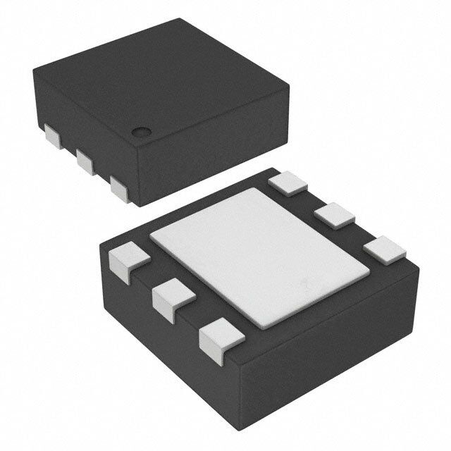
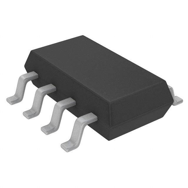
| 封装/外壳 | 6-WDFN 裸露焊盘 |
| 封装/箱体 | WSON-6 |
| 工作温度 | -40°C ~ 85°C |
| 工作温度范围 | - 40 C to + 85 C |
| 工厂包装数量 | 3000 |
| 开关频率 | 1.5 MHz |
| 拓扑结构 | Boost |
| 最大工作温度 | + 85 C |
| 最大输入电压 | 5.5 V |
| 最小工作温度 | - 40 C |
| 标准包装 | 3,000 |
| 电压-输入 | 2.7 V ~ 5.5 V |
| 电压-输出 | 5V |
| 电流-输出 | 140mA |
| 电源电流 | 90 uA |
| 类型 | 切换式电容器(充电泵) |
| 系列 | TPS60150 |
| 输入电压 | 2.7 V to 5.5 V |
| 输出数 | 1 |
| 输出电压 | 5 V |
| 输出电流 | 140 mA |
| 输出端数量 | 1 Output |
| 输出类型 | 固定 |
| 配用 | /product-detail/zh/TPS60150EVM-359/296-31212-ND/2232820 |
| 频率-开关 | 1.5MHz |


- 商务部:美国ITC正式对集成电路等产品启动337调查
- 曝三星4nm工艺存在良率问题 高通将骁龙8 Gen1或转产台积电
- 太阳诱电将投资9.5亿元在常州建新厂生产MLCC 预计2023年完工
- 英特尔发布欧洲新工厂建设计划 深化IDM 2.0 战略
- 台积电先进制程称霸业界 有大客户加持明年业绩稳了
- 达到5530亿美元!SIA预计今年全球半导体销售额将创下新高
- 英特尔拟将自动驾驶子公司Mobileye上市 估值或超500亿美元
- 三星加码芯片和SET,合并消费电子和移动部门,撤换高东真等 CEO
- 三星电子宣布重大人事变动 还合并消费电子和移动部门
- 海关总署:前11个月进口集成电路产品价值2.52万亿元 增长14.8%


PDF Datasheet 数据手册内容提取
Product Sample & Technical Tools & Support & Folder Buy Documents Software Community TPS60150 SLVS888C–DECEMBER2008–REVISEDOCTOBER2015 TPS60150 5-V, 140-mA Charge-Pump 1 Features 3 Description • 2.7-Vto5.5-VInputVoltageRange The TPS60150 device is a switched capacitor voltage 1 converter that produces a regulated, low noise, and • FixedOutputVoltageof5V low-ripple output voltage of 5 V from an unregulated • MaximumOutputCurrent:140mA inputvoltage. • 1.5-MHzSwitchingFrequency The 5-V output can supply a minimum of 140-mA • Typical90-μAQuiescentCurrentatNoLoad current. Condition(SkipMode) The TPS60150 device operates in skip mode when • X2ChargePump the load current falls less than 8 mA under typical • HardwareEnableandDisableFunction condition. In skip mode operation, quiescent current isreducedto90μA. • Built-inSoftStart • Built-inUndervoltageLockoutProtection Only 3 external capacitors are needed to generate theoutputvoltage,thereforesavingPCBspace. • ThermalandOvercurrentProtection • Availableina2-mm× 2-mm6-PinSONPackage Inrush current is limited by the soft-start function with0.8-mmHeight duringpoweronandpowertransientstates. The TPS60150 device operates over a free-air 2 Applications temperature range of –40°C to 85°C. The device is available with a small 2-mm × 2-mm 6-pin SON • USBOn-the-Go(OTG) package(QFN). • HDMI • PortableCommunicationDevices DeviceInformation(1) • PCMCIACards PARTNUMBER PACKAGE BODYSIZE(NOM) • MobilePhones,SmartPhones TPS60150 WSON(6) 2.00mm×2.00mm • HandheldMeters (1) For all available packages, see the orderable addendum at theendofthedatasheet. space space TypicalApplicationSchematic EfficiencyvsInputVoltage ENABLE 100 GND ENA /DISABLE 90 TA= 25°C 150 mA VIN VIN CP- C2 80 120 mA VOUT VOUT CP+ 2.2μF 70 50 mA (5.0V) 100 mA % C3 C1 y - 60 10 mA 2.2μF 4.7μF nc 50 e ci Effi 40 30 20 10 0 2.7 3.2 3.7 4.2 4.7 5.2 VI- Input Voltage - V 1 An IMPORTANT NOTICE at the end of this data sheet addresses availability, warranty, changes, use in safety-critical applications, intellectualpropertymattersandotherimportantdisclaimers.PRODUCTIONDATA.
TPS60150 SLVS888C–DECEMBER2008–REVISEDOCTOBER2015 www.ti.com Table of Contents 1 Features.................................................................. 1 7.3 FeatureDescription...................................................8 2 Applications........................................................... 1 7.4 DeviceFunctionalModes..........................................9 3 Description............................................................. 1 8 ApplicationandImplementation........................ 11 4 RevisionHistory..................................................... 2 8.1 ApplicationInformation............................................11 8.2 TypicalApplication .................................................11 5 PinConfigurationandFunctions......................... 3 9 PowerSupplyRecommendations...................... 16 6 Specifications......................................................... 4 10 Layout................................................................... 16 6.1 AbsoluteMaximumRatings......................................4 6.2 ESDRatings..............................................................4 10.1 LayoutGuidelines.................................................16 6.3 RecommendedOperatingConditions.......................4 10.2 LayoutExample....................................................16 6.4 ThermalInformation..................................................4 11 DeviceandDocumentationSupport................. 17 6.5 ElectricalCharacteristics...........................................5 11.1 CommunityResources..........................................17 6.6 TypicalCharacteristics..............................................6 11.2 Trademarks...........................................................17 7 DetailedDescription.............................................. 7 11.3 ElectrostaticDischargeCaution............................17 7.1 Overview...................................................................7 11.4 Glossary................................................................17 7.2 FunctionalBlockDiagram.........................................8 12 Mechanical,Packaging,andOrderable Information........................................................... 17 4 Revision History NOTE:Pagenumbersforpreviousrevisionsmaydifferfrompagenumbersinthecurrentversion. ChangesfromRevisionB(February2011)toRevisionC Page • AddedPinConfigurationandFunctionssection,ESDRatingstable,FeatureDescriptionsection,DeviceFunctional Modes,ApplicationandImplementationsection,PowerSupplyRecommendationssection,Layoutsection,Device andDocumentationSupportsection,andMechanical,Packaging,andOrderableInformationsection .............................. 1 ChangesfromRevisionA(April2009)toRevisionB Page • AddedtheThermalTableanddeletedtheDissipationRatingTable..................................................................................... 4 2 SubmitDocumentationFeedback Copyright©2008–2015,TexasInstrumentsIncorporated ProductFolderLinks:TPS60150
TPS60150 www.ti.com SLVS888C–DECEMBER2008–REVISEDOCTOBER2015 5 Pin Configuration and Functions DRVPackage 6-PinWSON TopView GND ENA VIN CP- VOUT CP+ PinFunctions PIN I/O DESCRIPTION NAME NO. CP+ 4 — Connecttotheflyingcapacitor CP– 5 — Connecttotheflyingcapacitor ENA 6 IN Hardwareenable/disablepin(High=Enable) GND 1 — Ground VIN 2 IN Supplyvoltageinput VOUT 3 OUT Output,connecttotheoutputcapacitor Copyright©2008–2015,TexasInstrumentsIncorporated SubmitDocumentationFeedback 3 ProductFolderLinks:TPS60150
TPS60150 SLVS888C–DECEMBER2008–REVISEDOCTOBER2015 www.ti.com 6 Specifications 6.1 Absolute Maximum Ratings Overoperatingfree-airtemperaturerange(unlessotherwisenoted) (1) MIN MAX UNIT V Inputvoltage(allpins) –0.3 7 V IN T Operatingtemperature –40 85 °C A T Maximumoperatingjunctiontemperature 150 °C J T Storagetemperature –55 150 °C stg (1) StressesbeyondthoselistedunderAbsoluteMaximumRatingsmaycausepermanentdamagetothedevice.Thesearestressratings onlyandfunctionaloperationofthedeviceattheseoranyotherconditionsbeyondthoseindicatedunderrecommendedoperating conditionsisnotimplied.Exposuretoabsolute-maximum-ratedconditionsforextendedperiodsmayaffectdevicereliability. 6.2 ESD Ratings VALUE UNIT Humanbodymodel(HBM),perANSI/ESDA/JEDECJS-001(1)(2) ±2000 V(ESD) Electrostaticdischarge Charged-devicemodel(CDM),perJEDECspecificationJESD22- V C101(3) ±500 (1) JEDECdocumentJEP155statesthat500-VHBMallowssafemanufacturingwithastandardESDcontrolprocess. (2) Thehumanbodymodel(HBM)isa100-pFcapacitordischargedthrougha1.5-kΩresistorintoeachpin.Thetestingisdoneaccording JEDECsEIA/JESD22-A114. (3) JEDECdocumentJEP157statesthat250-VCDMallowssafemanufacturingwithastandardESDcontrolprocess. 6.3 Recommended Operating Conditions MIN NOM MAX UNIT V Inputvoltage 2.7 5.5 V IN T Operatingambienttemperature –40 85 °C A T Operatingjunctiontemperature –40 125 °C J C Inputcapacitor 2.2 μF in C Outputcapacitor 2.2 μF o C Flyingcapacitor 1 μF f 6.4 Thermal Information TPS60150 THERMALMETRIC(1) DRV(WSON) UNIT 6PINS R Junction-to-ambientthermalresistance 69.1 °C/W θJA R Junction-to-case(top)thermalresistance 79.8 °C/W θJC(top) R Junction-to-boardthermalresistance 38.6 °C/W θJB ψ Junction-to-topcharacterizationparameter 1.2 °C/W JT ψ Junction-to-boardcharacterizationparameter 38.4 °C/W JB R Junction-to-case(bottom)thermalresistance 9.2 °C/W θJC(bot) (1) Formoreinformationabouttraditionalandnewthermalmetrics,seetheICPackageThermalMetricsapplicationreport,SPRA953. 4 SubmitDocumentationFeedback Copyright©2008–2015,TexasInstrumentsIncorporated ProductFolderLinks:TPS60150
TPS60150 www.ti.com SLVS888C–DECEMBER2008–REVISEDOCTOBER2015 6.5 Electrical Characteristics V =3.6V,T =–40°Cto85°C,typicalvaluesareatT =25°C,C1=C3=2.2μF,C2=1μF(unlessotherwisenoted) IN A A PARAMETER TESTCONDITIONS MIN TYP MAX UNIT POWERSTAGE V Inputvoltagerange 2.7 5.5 V IN V Undervoltagelockoutthreshold 1.9 2.1 V UVLO I Operatingquiescentcurrent I =140mA,Enable=V 4.7 mA Q OUT IN Skipmodeoperatingquiescent IOUT=0mA,Enable=VIN(noswitching) 80 μA I Qskip current I =0mA,Enable=V (minimumswitching) 90 μA OUT IN I Shutdowncurrent 2.7V≤V ≤5.5V,Enable=0V 1 μA SD IN V Outputvoltage(1) I ≤50mA,2.7V≤V <5.5V 4.8 5 5.2 V OUT OUT IN V Skipmodeoutputvoltage I =0mA,2.7V≤V ≤5.5V V +0.1 V OUT(skip) OUT IN OUT F Switchingfrequency 1.5 MHz SW SS Soft-starttime Fromtherisingedgeofenableto90%output 150 μs TIME OUTPUTCURRENT V remainsfrom4.8Vto5.2V, OUT 120 IOUT_nom Maximumoutputcurrent 3.1V≤VIN≤5.5V mA 3.3V<V <5.5V 140 IN I Shortcircuitcurrent(2) V =0V 80 mA OUT_short OUT RIPPLEVOLTAGE V Outputripplevoltage I =140mA 30 mV R OUT ENABLECONTROL V Logichighinputvoltage 2.7V≤V ≤5.5V 1.3 V V HI IN IN V Logiclowinputvoltage –0.2 0.4 V LI I Logichighinputcurrent 1 μA HI I Logiclowinputcurrent 1 μA LI THERMALSHUTDOWN T Shutdowntemperature 160 °C SD T Shutdownrecovery 140 °C RC (1) Wheninskipmode,outputvoltagecanexceedV specbecauseV =V +0.1. OUT OUT(skip) OUT (2) TheTPS60150devicehasinternalprotectioncircuittoprotectICwhenV shortedtoGND. OUT Copyright©2008–2015,TexasInstrumentsIncorporated SubmitDocumentationFeedback 5 ProductFolderLinks:TPS60150
TPS60150 SLVS888C–DECEMBER2008–REVISEDOCTOBER2015 www.ti.com 6.6 Typical Characteristics 120 0.3 TA= -40°C No load 110 No Switching 0.25 A Input Current -Aµ1089000 -85°C Max Output Current - 0.001..152 TA= 25°C TA= 85°C 25°C -40°C - O I 70 0.05 60 0 2.7 3.2 3.7 4.2 4.7 5.2 2.7 3.2 3.7 4.2 4.7 5.2 VI- Input Voltage - V VI- Input Voltage - V Figure1.QuiescentCurrentvsInputVoltage Figure2.MaximumOutputCurrentvsInputVoltageat Temperature 6 SubmitDocumentationFeedback Copyright©2008–2015,TexasInstrumentsIncorporated ProductFolderLinks:TPS60150
TPS60150 www.ti.com SLVS888C–DECEMBER2008–REVISEDOCTOBER2015 7 Detailed Description 7.1 Overview The TPS60150 regulated charge pump provides a regulated output voltage for various input voltages. The TPS60150 device regulates the voltage across the flying capacitor to 2.5 V and controls the voltage drop of Q1 andQ2whileaconversionclockwith50%dutycycledrivestheFETs. VIN Q1 Q2 OFF ON 2.5V - + Q3 CF Q4 ON OFF VOUT C OUT Figure3. ChargingMode During the first half cycle, Q2 and Q3 transistors are turned on and flying capacitor, C , will be charged to 2.5 V F ideally. VIN Q1 Q2 ON VQ1 OFF 2.5V - + Q3 CF Q4 OFF ON VOUT C OUT Figure4. DischargingMode During the second half cycle, Q1 and Q4 transistors are turned on. Capacitor C will then be discharged to F output. UseEquation1tocalculatetheoutputvoltage. V = V - VQ1 + V(C ) - VQ4 = V - VQ1 + 2.5 V - VQ4 = 5 V OUT IN F IN (Ideal) (1) Theoutputvoltageisregulatedbyoutputfeedbackandaninternallycompensatedvoltagecontrolloop. Copyright©2008–2015,TexasInstrumentsIncorporated SubmitDocumentationFeedback 7 ProductFolderLinks:TPS60150
TPS60150 SLVS888C–DECEMBER2008–REVISEDOCTOBER2015 www.ti.com 7.2 Functional Block Diagram C F CP- CP+ 5 4 VIN TPS60150 2 TSD Regulation Φ2 Φ1 UVLO Current Limit Soft Start Φ1 Φ2 VOUT V Bias circuit REF 3 ErrorAmp Control + R1 - ENA R2 6 Enable IC OSC + 1.5 MHz - Skip Comp 1 GND 7.3 Feature Description 7.3.1 Enable An enable pin on the regulator is used to place the device into an energy-saving shutdown mode. In this mode, theoutputisdisconnectedfromtheinput,andtheinputquiescentcurrentisreducedto10 μAmaximum. 7.3.2 UndervoltageLockout When the input voltage drops, the undervoltage lockout prevents misoperation by switching off the device. The converterstartsoperationagainwhentheinputvoltageexceedsthethreshold,providedtheenablepinishigh. 7.3.3 ThermalShutdownProtection The regulator has thermal shutdown circuitry that protects it from damage caused by overload conditions. The thermal protection circuitry disables the output when the junction temperature reached approximately 160°C, allowing the device to cool. When the junction temperature cools to approximately 140°C, the output circuitry is automatically reenabled. Continuously running the regulator into thermal shutdown can degrade reliability. The regulatoralsoprovidescurrentlimittoprotectitselfandtheload. 8 SubmitDocumentationFeedback Copyright©2008–2015,TexasInstrumentsIncorporated ProductFolderLinks:TPS60150
TPS60150 www.ti.com SLVS888C–DECEMBER2008–REVISEDOCTOBER2015 7.4 Device Functional Modes 7.4.1 SoftStart Aninternalsoftstartlimitstheinrushcurrentwhenthedeviceisbeingenabled. 7.4.2 NormalModeandSkipModeOperation The TPS60150 device has skip mode operation as shown in Figure 5. The TPS60150 device enters skip mode if the output voltage reaches 5 V +0.1 V and the load current is less than 8 mA (typical). In skip mode, the TPS60150 device disables the oscillator and decreases the prebias current of the output stage to reduce the power consumption. Once the output voltage dips less than the threshold voltage of 5 V +0.1 V, the TPS60150 device begins switching to increase output voltage until the output reaches 5 V +0.1 V. When the output voltage dips less than 5 V, the TPS60150 device returns to normal pulse width modulation (PWM) mode; thereby reenablingtheoscillatorandincreasingtheprebiascurrentoftheoutputstagetosupplyoutputcurrent. Theskipthresholdvoltageandcurrentdependoninputvoltageandoutputcurrentconditions. Quiescent Current 4.7 mA 90mA t Load current 50 mA No load t V OUT 5 V +0.1 V 5 V t Gate Waveform Of Q1Transistor t Start up Skip Mode at Normal Mode at Skip Mode at Waveform No Load Condition 50mALoad Current No Load Condition Figure5. NormalModeandSkipModeOperation 7.4.3 ShortCircuitProtection The TPS60150 device has internal short circuit protection to protect the IC when the output is shorted to ground. To avoid damage when output is shorted to ground, the short circuit protection circuitry senses output voltage andclampsthemaximumoutputcurrentto80mA(typical). Copyright©2008–2015,TexasInstrumentsIncorporated SubmitDocumentationFeedback 9 ProductFolderLinks:TPS60150
TPS60150 SLVS888C–DECEMBER2008–REVISEDOCTOBER2015 www.ti.com Device Functional Modes (continued) EN VOUT t 5.0V 4.5V 4.2V Vout t Current Limit 300mA I OUT_MAX Output current Output 50mA(min) Short circuit current t0 t1 t2 t Soft Start Vout is short to GND Figure6. MaximumOutputCurrentCapabilityandShortCircuitProtection 10 SubmitDocumentationFeedback Copyright©2008–2015,TexasInstrumentsIncorporated ProductFolderLinks:TPS60150
TPS60150 www.ti.com SLVS888C–DECEMBER2008–REVISEDOCTOBER2015 8 Application and Implementation NOTE Information in the following applications sections is not part of the TI component specification, and TI does not warrant its accuracy or completeness. TI’s customers are responsible for determining suitability of components for their purposes. Customers should validateandtesttheirdesignimplementationtoconfirmsystemfunctionality. 8.1 Application Information Most of today’s battery-powered portable electronics allow and/or require data transfer with a PC. One of the fastest data transfer protocols is through USB On-the-Go (OTG). As Figure 7 shows, the USB OTG circuitry in theportabledevicerequiresa5-Vpowerrailandupto140mAofcurrent.TheTPS60150devicemaybeusedto providea5-Vpowerrailinabatterypoweredsystem. 8.2 Typical Application 8.2.1 USBOntheGoCircuitry GND ENA VIN = 2.7 V - 5.5 V VIN CP- C2 VOUT CP+ 1mF 140mA(VIN > 3.3V) C3 C1 50mA(VIN > 2.7V) 2.2mF 2.2mF 5 V VBUS Controller GND ID USB Transceiver Comparator D+ D- Figure7. ApplicationCircuitforOTGSystem 8.2.1.1 DesignRequirements The design guideline provides a component selection to operate the device within the Recommended Operating Conditions. 8.2.1.2 DetailedDesignProcedure 8.2.1.2.1 CapacitorSelection For minimum output voltage ripple, the output capacitor (C ) should be a surface-mount ceramic capacitor. OUT Tantalum capacitors generally have a higher effective series resistance (ESR) and may contribute to higher output voltage ripple. Leaded capacitors also increase ripple due to the higher inductance of the package itself. To achieve the best operation with low input voltage and high load current, the input and flying capacitors (C IN andC ,respectively)shouldalsobesurface-mountceramictypes. F Copyright©2008–2015,TexasInstrumentsIncorporated SubmitDocumentationFeedback 11 ProductFolderLinks:TPS60150
TPS60150 SLVS888C–DECEMBER2008–REVISEDOCTOBER2015 www.ti.com Typical Application (continued) ENABLE GND ENA /DISABLE VIN VIN CP- VOUT VOUT CP+ CF (5 V) C C OUT IN Figure8. Capacitors Generally,C canbecalculatedusingEquation2. FLY Q =c ´ v=C ´ DV , charging FLY CFLY æTö Qdischarging=idischarge ´ t=2 ´ ILOAD(MAX) ´ ç ÷,halfduty. è2ø (2) æTö Bothequationshouldbesame,\2 ´ ILOAD(MAX) ´ çè 2÷ø =CFLY ´ DVCFLY æTö 2 ´ ILOAD(MAX) ´ çè2÷ø ILOAD(MAX) \C ³ = FLY DV DV ´ ¦ CFLY CFLY (3) IfI =140mA,f=1.5MHZ,and ΔV =100mV,theminimumvalueoftheflyingcapacitorshouldbe1 μF. LOAD CFLY Outputcapacitance,C ,isalsostronglyrelatedtooutputripplevoltageandloopstability, OUT I LOAD(MAX) V = +2I ´ESR OUT(RIPPLE) (2´f´C ) LOAD(MAX) COUT OUT (4) The minimum output capacitance for all output levels is 2.2 μF due to control stability. Larger ceramic capacitors orlowESRcapacitorscanbeusedtolowertheoutputripplevoltage. Table1.SuggestedCapacitors(Input,Output,andFlyingCapacitor) VALUE DIELECTRICMATERIAL PACKAGESIZE RATEDVOLTAGE 4.7μF X5RorX7R 0603 10V 2.2μF X5RorX7R 0603 10V The efficiency of the charge pump regulator varies with the output voltage, the applied input voltage and the load current. UseEquation5andEquation6tocalculatetheapproximateefficiencyinnormaloperatingmodeisgivenby: PD(out) V ´ I Efficiency(%)= ´ 100= OUT OUT ´ 100,I = 2 ´ I +I PD(in) V ´ I IN OUT Q IN IN (5) V Efficiency(%) = OUT ×100 (I =2 ´ I ) Quiescent current was neglected. IN OUT 2 ×V IN (6) 12 SubmitDocumentationFeedback Copyright©2008–2015,TexasInstrumentsIncorporated ProductFolderLinks:TPS60150
TPS60150 www.ti.com SLVS888C–DECEMBER2008–REVISEDOCTOBER2015 8.2.1.3 ApplicationCurves 5.25 5.10 TA= 25°C TA= 25°C 5.2 5.05 5.15 10 mA 50 mA V V ge - 5.1 ge - 5.00 utput Volta 5.05 3.6 V 4.2 V utput Volta 4.95 112500 mmAA O 5 O - O - O 4.90 V 4.95 5 V 5.5 V V 100 mA 4.85 4.9 2.7 V 4.85 4.80 0 0.05 0.1 0.15 0.2 2.7 3.2 3.7 4.2 4.7 5.2 IO- Output Current -A VI- Input Voltage - V Figure9.OutputVoltagevsOutputCurrent Figure10.OutputVoltagevsInputVoltage 100 90 TA= 25°C 150 mA 80 120 mA 70 50 mA 100 mA % y - 60 10 mA c en 50 ci Effi 40 30 20 10 0 2.7 3.2 3.7 4.2 4.7 5.2 VI- Input Voltage - V 20ms/div Figure11.EfficiencyvsInputVoltage Figure12.LoadTransientResponse V =2.7V,IO=30mAto50mA IN 20ms/div 5 ms/div Figure13.LoadTransientResponse Figure14. OutputRippleVoltage(SkipMode) VIN=3.6V,IO=60mAto100mA VIN=2.7V,IO=0mA Copyright©2008–2015,TexasInstrumentsIncorporated SubmitDocumentationFeedback 13 ProductFolderLinks:TPS60150
TPS60150 SLVS888C–DECEMBER2008–REVISEDOCTOBER2015 www.ti.com 5 ms/div 500 ns/div Figure15.OutputRippleVoltage(SkipMode) Figure16.OutputRippleVoltage(NormalMode) VIN=3.6V,IO=0mA VIN=2.7V,IO=50mA 500 ns/div 1 ms/div Figure17.OutputRipple(NormalMode) Figure18.PowerOn V =3.6V,IO=100mA V =2.7V,IO=50mA IN IN 1 ms/div 200ms/div Figure19.PowerOn Figure20.Enable/Disable VIN=3.6V,IO=100mA VIN=2.7V,IO=50mA 14 SubmitDocumentationFeedback Copyright©2008–2015,TexasInstrumentsIncorporated ProductFolderLinks:TPS60150
TPS60150 www.ti.com SLVS888C–DECEMBER2008–REVISEDOCTOBER2015 200ms/div 50 ms/div Figure21.Enable/Disable Figure22.ThermalShutdownOperation VIN=3.6V,IO=100mA VIN=5.5V,RLOAD=20Ω 8.2.2 SystemExample Low-cost portable electronics with small LCD displays require a low-cost solution for providing the WLED backlight.AsshowninFigure23,theTPS60150devicecanalsobeusedtodriveseveralWLEDsinparallel,with thehelpofballastresistors. VIN = 2.7 V~5.5 V GND ENA ENABLE 140mA(VIN > 3.3V) VIN CP- C2 50mA(VIN > 2.7V) 1mF VOUT CP+ C3 C1 2.2mF 2.2mF Figure23. ApplicationCircuitforDrivingWhiteLEDs Copyright©2008–2015,TexasInstrumentsIncorporated SubmitDocumentationFeedback 15 ProductFolderLinks:TPS60150
TPS60150 SLVS888C–DECEMBER2008–REVISEDOCTOBER2015 www.ti.com 9 Power Supply Recommendations The TPS60150 device has no special requirements for its input power supply. The input power supply's output current must be rated according to the supply voltage, output voltage and output current of the TPS60150 device. 10 Layout 10.1 Layout Guidelines Large transient currents flow in the VIN, VOUT, and GND traces. To minimize both input and output ripple, keep thecapacitorsascloseaspossibletotheregulatorusingshort,directcircuittraces. 10.2 Layout Example GND VIN GND VOUT Figure24. RecommendedPCBLayout 16 SubmitDocumentationFeedback Copyright©2008–2015,TexasInstrumentsIncorporated ProductFolderLinks:TPS60150
TPS60150 www.ti.com SLVS888C–DECEMBER2008–REVISEDOCTOBER2015 11 Device and Documentation Support 11.1 Community Resources The following links connect to TI community resources. Linked contents are provided "AS IS" by the respective contributors. They do not constitute TI specifications and do not necessarily reflect TI's views; see TI's Terms of Use. TIE2E™OnlineCommunity TI'sEngineer-to-Engineer(E2E)Community.Createdtofostercollaboration amongengineers.Ate2e.ti.com,youcanaskquestions,shareknowledge,exploreideasandhelp solveproblemswithfellowengineers. DesignSupport TI'sDesignSupport QuicklyfindhelpfulE2Eforumsalongwithdesignsupporttoolsand contactinformationfortechnicalsupport. 11.2 Trademarks E2EisatrademarkofTexasInstruments. Allothertrademarksarethepropertyoftheirrespectiveowners. 11.3 Electrostatic Discharge Caution Thesedeviceshavelimitedbuilt-inESDprotection.Theleadsshouldbeshortedtogetherorthedeviceplacedinconductivefoam duringstorageorhandlingtopreventelectrostaticdamagetotheMOSgates. 11.4 Glossary SLYZ022—TIGlossary. Thisglossarylistsandexplainsterms,acronyms,anddefinitions. 12 Mechanical, Packaging, and Orderable Information The following pages include mechanical, packaging, and orderable information. This information is the most current data available for the designated devices. This data is subject to change without notice and revision of thisdocument.Forbrowser-basedversionsofthisdatasheet,refertotheleft-handnavigation. Copyright©2008–2015,TexasInstrumentsIncorporated SubmitDocumentationFeedback 17 ProductFolderLinks:TPS60150
PACKAGE OPTION ADDENDUM www.ti.com 2-Jun-2016 PACKAGING INFORMATION Orderable Device Status Package Type Package Pins Package Eco Plan Lead/Ball Finish MSL Peak Temp Op Temp (°C) Device Marking Samples (1) Drawing Qty (2) (6) (3) (4/5) TPS60150DRVR ACTIVE WSON DRV 6 3000 Green (RoHS CU NIPDAU Level-1-260C-UNLIM -40 to 85 CGO & no Sb/Br) TPS60150DRVT ACTIVE WSON DRV 6 250 Green (RoHS CU NIPDAU Level-1-260C-UNLIM -40 to 85 CGO & no Sb/Br) (1) The marketing status values are defined as follows: ACTIVE: Product device recommended for new designs. LIFEBUY: TI has announced that the device will be discontinued, and a lifetime-buy period is in effect. NRND: Not recommended for new designs. Device is in production to support existing customers, but TI does not recommend using this part in a new design. PREVIEW: Device has been announced but is not in production. Samples may or may not be available. OBSOLETE: TI has discontinued the production of the device. (2) Eco Plan - The planned eco-friendly classification: Pb-Free (RoHS), Pb-Free (RoHS Exempt), or Green (RoHS & no Sb/Br) - please check http://www.ti.com/productcontent for the latest availability information and additional product content details. TBD: The Pb-Free/Green conversion plan has not been defined. Pb-Free (RoHS): TI's terms "Lead-Free" or "Pb-Free" mean semiconductor products that are compatible with the current RoHS requirements for all 6 substances, including the requirement that lead not exceed 0.1% by weight in homogeneous materials. Where designed to be soldered at high temperatures, TI Pb-Free products are suitable for use in specified lead-free processes. Pb-Free (RoHS Exempt): This component has a RoHS exemption for either 1) lead-based flip-chip solder bumps used between the die and package, or 2) lead-based die adhesive used between the die and leadframe. The component is otherwise considered Pb-Free (RoHS compatible) as defined above. Green (RoHS & no Sb/Br): TI defines "Green" to mean Pb-Free (RoHS compatible), and free of Bromine (Br) and Antimony (Sb) based flame retardants (Br or Sb do not exceed 0.1% by weight in homogeneous material) (3) MSL, Peak Temp. - The Moisture Sensitivity Level rating according to the JEDEC industry standard classifications, and peak solder temperature. (4) There may be additional marking, which relates to the logo, the lot trace code information, or the environmental category on the device. (5) Multiple Device Markings will be inside parentheses. Only one Device Marking contained in parentheses and separated by a "~" will appear on a device. If a line is indented then it is a continuation of the previous line and the two combined represent the entire Device Marking for that device. (6) Lead/Ball Finish - Orderable Devices may have multiple material finish options. Finish options are separated by a vertical ruled line. Lead/Ball Finish values may wrap to two lines if the finish value exceeds the maximum column width. Important Information and Disclaimer:The information provided on this page represents TI's knowledge and belief as of the date that it is provided. TI bases its knowledge and belief on information provided by third parties, and makes no representation or warranty as to the accuracy of such information. Efforts are underway to better integrate information from third parties. TI has taken and continues to take reasonable steps to provide representative and accurate information but may not have conducted destructive testing or chemical analysis on incoming materials and chemicals. TI and TI suppliers consider certain information to be proprietary, and thus CAS numbers and other limited information may not be available for release. Addendum-Page 1
PACKAGE OPTION ADDENDUM www.ti.com 2-Jun-2016 In no event shall TI's liability arising out of such information exceed the total purchase price of the TI part(s) at issue in this document sold by TI to Customer on an annual basis. Addendum-Page 2
PACKAGE MATERIALS INFORMATION www.ti.com 29-May-2019 TAPE AND REEL INFORMATION *Alldimensionsarenominal Device Package Package Pins SPQ Reel Reel A0 B0 K0 P1 W Pin1 Type Drawing Diameter Width (mm) (mm) (mm) (mm) (mm) Quadrant (mm) W1(mm) TPS60150DRVR WSON DRV 6 3000 178.0 8.4 2.25 2.25 1.0 4.0 8.0 Q2 TPS60150DRVR WSON DRV 6 3000 180.0 8.4 2.3 2.3 1.15 4.0 8.0 Q2 TPS60150DRVT WSON DRV 6 250 178.0 8.4 2.25 2.25 1.0 4.0 8.0 Q2 TPS60150DRVT WSON DRV 6 250 180.0 8.4 2.3 2.3 1.15 4.0 8.0 Q2 PackMaterials-Page1
PACKAGE MATERIALS INFORMATION www.ti.com 29-May-2019 *Alldimensionsarenominal Device PackageType PackageDrawing Pins SPQ Length(mm) Width(mm) Height(mm) TPS60150DRVR WSON DRV 6 3000 205.0 200.0 33.0 TPS60150DRVR WSON DRV 6 3000 182.0 182.0 20.0 TPS60150DRVT WSON DRV 6 250 205.0 200.0 33.0 TPS60150DRVT WSON DRV 6 250 182.0 182.0 20.0 PackMaterials-Page2
GENERIC PACKAGE VIEW DRV 6 WSON - 0.8 mm max height PLASTIC SMALL OUTLINE - NO LEAD Images above are just a representation of the package family, actual package may vary. Refer to the product data sheet for package details. 4206925/F
PACKAGE OUTLINE DRV0006A WSON - 0.8 mm max height SCALE 5.500 PLASTIC SMALL OUTLINE - NO LEAD B 2.1 A 1.9 PIN 1 INDEX AREA 2.1 1.9 0.8 C 0.7 SEATING PLANE 0.08 C (0.2) TYP 1 0.1 0.05 EXPOSED 0.00 THERMAL PAD 3 4 2X 7 1.3 1.6 0.1 6 1 4X 0.65 0.35 6X PIN 1 ID 0.3 0.25 6X (OPTIONAL) 0.2 0.1 C A B 0.05 C 4222173/B 04/2018 NOTES: 1. All linear dimensions are in millimeters. Any dimensions in parenthesis are for reference only. Dimensioning and tolerancing per ASME Y14.5M. 2. This drawing is subject to change without notice. 3. The package thermal pad must be soldered to the printed circuit board for thermal and mechanical performance. www.ti.com
EXAMPLE BOARD LAYOUT DRV0006A WSON - 0.8 mm max height PLASTIC SMALL OUTLINE - NO LEAD 6X (0.45) (1) 1 7 6X (0.3) 6 SYMM (1.6) (1.1) 4X (0.65) 4 3 (R0.05) TYP SYMM ( 0.2) VIA (1.95) TYP LAND PATTERN EXAMPLE SCALE:25X 0.07 MAX 0.07 MIN ALL AROUND ALL AROUND SOLDER MASK METAL METAL UNDER SOLDER MASK OPENING SOLDER MASK OPENING NON SOLDER MASK DEFINED SOLDER MASK (PREFERRED) DEFINED SOLDER MASK DETAILS 4222173/B 04/2018 NOTES: (continued) 4. This package is designed to be soldered to a thermal pad on the board. For more information, see Texas Instruments literature number SLUA271 (www.ti.com/lit/slua271). 5. Vias are optional depending on application, refer to device data sheet. If some or all are implemented, recommended via locations are shown. www.ti.com
EXAMPLE STENCIL DESIGN DRV0006A WSON - 0.8 mm max height PLASTIC SMALL OUTLINE - NO LEAD SYMM 6X (0.45) METAL 1 7 6X (0.3) 6 (0.45) SYMM 4X (0.65) (0.7) 4 3 (R0.05) TYP (1) (1.95) SOLDER PASTE EXAMPLE BASED ON 0.125 mm THICK STENCIL EXPOSED PAD #7 88% PRINTED SOLDER COVERAGE BY AREA UNDER PACKAGE SCALE:30X 4222173/B 04/2018 NOTES: (continued) 6. Laser cutting apertures with trapezoidal walls and rounded corners may offer better paste release. IPC-7525 may have alternate design recommendations. www.ti.com
IMPORTANTNOTICEANDDISCLAIMER TIPROVIDESTECHNICALANDRELIABILITYDATA(INCLUDINGDATASHEETS),DESIGNRESOURCES(INCLUDINGREFERENCE DESIGNS),APPLICATIONOROTHERDESIGNADVICE,WEBTOOLS,SAFETYINFORMATION,ANDOTHERRESOURCES“ASIS” ANDWITHALLFAULTS,ANDDISCLAIMSALLWARRANTIES,EXPRESSANDIMPLIED,INCLUDINGWITHOUTLIMITATIONANY IMPLIEDWARRANTIESOFMERCHANTABILITY,FITNESSFORAPARTICULARPURPOSEORNON-INFRINGEMENTOFTHIRD PARTYINTELLECTUALPROPERTYRIGHTS. TheseresourcesareintendedforskilleddevelopersdesigningwithTIproducts.Youaresolelyresponsiblefor(1)selectingtheappropriate TIproductsforyourapplication,(2)designing,validatingandtestingyourapplication,and(3)ensuringyourapplicationmeetsapplicable standards,andanyothersafety,security,orotherrequirements.Theseresourcesaresubjecttochangewithoutnotice.TIgrantsyou permissiontousetheseresourcesonlyfordevelopmentofanapplicationthatusestheTIproductsdescribedintheresource.Other reproductionanddisplayoftheseresourcesisprohibited.NolicenseisgrantedtoanyotherTIintellectualpropertyrightortoanythird partyintellectualpropertyright.TIdisclaimsresponsibilityfor,andyouwillfullyindemnifyTIanditsrepresentativesagainst,anyclaims, damages,costs,losses,andliabilitiesarisingoutofyouruseoftheseresources. TI’sproductsareprovidedsubjecttoTI’sTermsofSale(www.ti.com/legal/termsofsale.html)orotherapplicabletermsavailableeitheron ti.comorprovidedinconjunctionwithsuchTIproducts.TI’sprovisionoftheseresourcesdoesnotexpandorotherwisealterTI’sapplicable warrantiesorwarrantydisclaimersforTIproducts. MailingAddress:TexasInstruments,PostOfficeBox655303,Dallas,Texas75265 Copyright©2019,TexasInstrumentsIncorporated