ICGOO在线商城 > TPS60123PWP
 Datasheet下载
- 型号: TPS60123PWP
- 制造商: Texas Instruments
- 库位|库存: xxxx|xxxx
- 要求:
| 数量阶梯 | 香港交货 | 国内含税 |
| +xxxx | $xxxx | ¥xxxx |
查看当月历史价格
查看今年历史价格
TPS60123PWP产品简介:
ICGOO电子元器件商城为您提供TPS60123PWP由Texas Instruments设计生产,在icgoo商城现货销售,并且可以通过原厂、代理商等渠道进行代购。 提供TPS60123PWP价格参考以及Texas InstrumentsTPS60123PWP封装/规格参数等产品信息。 你可以下载TPS60123PWP参考资料、Datasheet数据手册功能说明书, 资料中有TPS60123PWP详细功能的应用电路图电压和使用方法及教程。
| 参数 | 数值 |
| 产品目录 | 集成电路 (IC)半导体 |
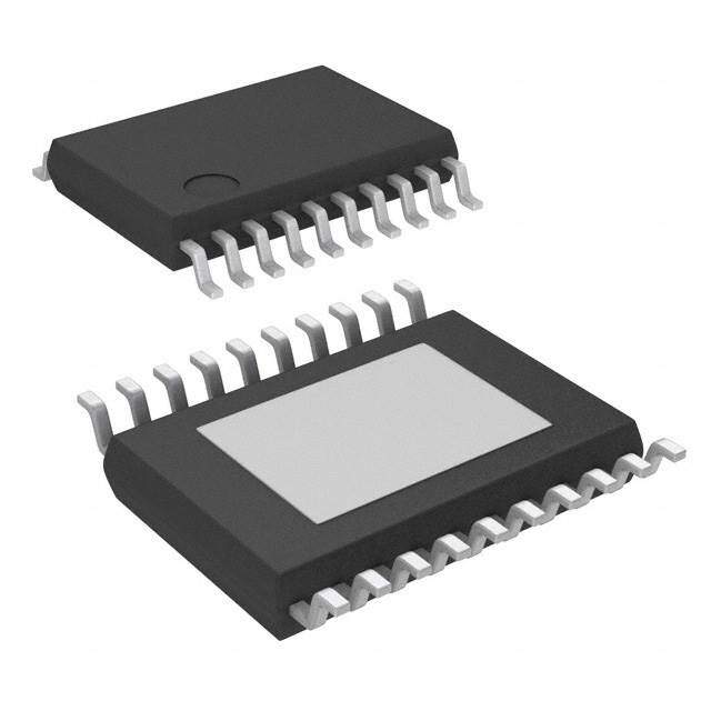
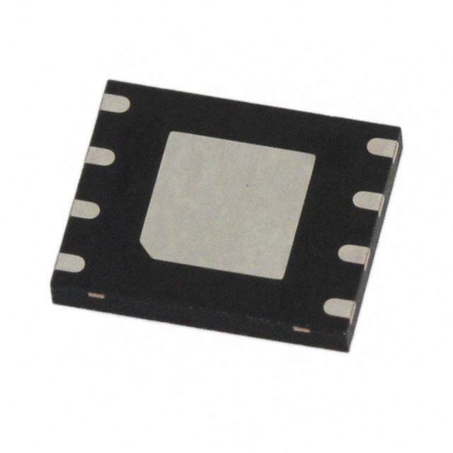
| 描述 | IC REG BST SWITCHED CAP 20HTSSOP稳压器—开关式稳压器 Reg 3.3V Hi-Eff Chrg Pump DC/DC Converter |
| 产品分类 | |
| 品牌 | Texas Instruments |
| 产品手册 | |
| 产品图片 |
|
| rohs | 符合RoHS无铅 / 符合限制有害物质指令(RoHS)规范要求 |
| 产品系列 | 电源管理 IC,稳压器—开关式稳压器,Texas Instruments TPS60123PWP- |
| 数据手册 | |
| 产品型号 | TPS60123PWP |
| PWM类型 | - |
| 产品目录页面 | |
| 产品种类 | 稳压器—开关式稳压器 |
| 供应商器件封装 | 20-HTSSOP |
| 其它名称 | 296-2270-5 |
| 包装 | 管件 |
| 单位重量 | 81.800 mg |
| 同步整流器 | 无 |
| 商标 | Texas Instruments |
| 安装类型 | 表面贴装 |
| 安装风格 | SMD/SMT |
| 宽度 | 4.4 mm |
| 封装 | Tube |
| 封装/外壳 | 20-TSSOP(0.173",4.40mm 宽)裸焊盘 |
| 封装/箱体 | HTSSOP-20 |
| 工作温度 | -40°C ~ 85°C |
| 工作温度范围 | - 40 C to + 85 C |
| 工厂包装数量 | 70 |
| 开关频率 | 320 kHz |
| 拓扑结构 | Boost |
| 最大工作温度 | + 85 C |
| 最大输入电压 | 3.6 V |
| 最小工作温度 | - 40 C |
| 最小输入电压 | 1.8 V |
| 标准包装 | 70 |
| 电压-输入 | 1.8 V ~ 3.6 V |
| 电压-输出 | 3.3V |
| 电流-输出 | 100mA |
| 类型 | 升压(升压),切换电容(充电泵) |
| 系列 | TPS60123 |
| 输入电压 | 1.8 V to 3.6 V |
| 输出数 | 1 |
| 输出电压 | 3.3 V |
| 输出电流 | 100 mA |
| 输出端数量 | 1 Output |
| 输出类型 | 固定 |
| 频率-开关 | 320kHz |


- 商务部:美国ITC正式对集成电路等产品启动337调查
- 曝三星4nm工艺存在良率问题 高通将骁龙8 Gen1或转产台积电
- 太阳诱电将投资9.5亿元在常州建新厂生产MLCC 预计2023年完工
- 英特尔发布欧洲新工厂建设计划 深化IDM 2.0 战略
- 台积电先进制程称霸业界 有大客户加持明年业绩稳了
- 达到5530亿美元!SIA预计今年全球半导体销售额将创下新高
- 英特尔拟将自动驾驶子公司Mobileye上市 估值或超500亿美元
- 三星加码芯片和SET,合并消费电子和移动部门,撤换高东真等 CEO
- 三星电子宣布重大人事变动 还合并消费电子和移动部门
- 海关总署:前11个月进口集成电路产品价值2.52万亿元 增长14.8%

PDF Datasheet 数据手册内容提取
TPS60120, TPS60121, TPS60122, TPS60123, TPS60124, TPS60125 REGULATED 200-mA HIGH EFFICIENCY CHARGE PUMP DC/DC CONVERTERS SLVS257B – NOVEMBER 1999 – REVISED AUGUST 2000 features applications (cid:0) (cid:0) High Average Efficiency Over Input Voltage Applications Powered by Two Battery Cells Range Because of Special Switching (cid:0) Portable Instruments Topology (cid:0) Battery-Powered Microprocessor Systems (cid:0) Minimum 200-mA Output Current From an (cid:0) Miniature Equipment Input Voltage Range of 1.8-V to 3.6-V (cid:0) (cid:0) Backup-Battery Boost Converters Regulated 3.3-V or 3-V ±4% Output Voltage (cid:0) (cid:0) PDAs, Organizers, Laptops No Inductors Required, Low EMI (cid:0) (cid:0) MP-3 Portable Audio Players Only Four External Components Required (cid:0) (cid:0) Handheld Instrumentation 55-m A Quiescent Supply Current (cid:0) (cid:0) Medical Instruments (e.g., Glucose Meters) 0.05-m A Shutdown Current (cid:0) (cid:0) Cordless Phones Load Disconnected in Shutdown (cid:0) Integrated Low Battery and Power Good Detectors efficiency (TPS60120, TPS60121) (cid:0) Evaluation Module Available 100 (TPS60120EVM-142) IO = 66 mA VO = 3.3 V · 90 TC = 25°C description 80 The TPS6012x step-up, regulated charge pumps 70 generate a 3.3-V or 3-V ±4% output voltage from – % 60 IO = 116 mA IO = 164 mA a 1.8-V to 3.6-V input voltage (two alkaline, NiCd, cy or NiMH batteries). They can deliver an output en 50 IO = 216 mA ci current of at least 200 mA (100 mA for the Effi 40 TPS60122 and TPS60123), all from a 2-V input. 30 Four external capacitors are needed to build a complete high efficiency dc/dc charge pump 20 converter. To achieve the high efficiency over a 10 wide input voltage range, the charge pump automatically selects between a 1.5x or doubler 0 1.8 2 2.2 2.4 2.6 2.8 3 3.2 3.4 3.6 conversion mode. From a 2-V input, all ICs can start with full load current. VI – Input Voltage – V typical operating circuit The devices feature the power-saving pulse-skip Input Output mode to extend battery life at light loads. TPS60120 1.8 V to 3.6 V 3.3 V TPS60120, TPS60122, and TPS60124 include a IN OUT low battery comparator. TPS60121, TPS60123, and TPS60125 feature a power-good output. The Ci R1 IN OUT CO logic shutdown function reduces the supply 10 m F 22 m F LBI FB current to a maximum of 1m A and disconnects the R3 load from the input. Special current-control R2 LBO circuitry prevents excessive current from being C1+ C2+ drawn from the battery during start-up. This dc/dc C1 C2 converter requires no inductors, therefore EMI is 2.2 m F C1– C2– 2.2 m F of low concern. It is available in the small, thermally enhanced 20-pin PowerPAD(cid:1) package ENABLE (PWP). OFF/ON PGND GND Please be aware that an important notice concerning availability, standard warranty, and use in critical applications of TexasInstruments semiconductor products and disclaimers thereto appears at the end of this data sheet. PowerPAD is a trademark of Texas Instruments Incorporated. PRODUCTION DATA information is current as of publication date. Copyright 2000, Texas Instruments Incorporated Products conform to specifications per the terms of Texas Instruments standard warranty. Production processing does not necessarily include testing of all parameters. POST OFFICE BOX 655303 • DALLAS, TEXAS 75265 1
TPS60120, TPS60121, TPS60122, TPS60123, TPS60124, TPS60125 REGULATED 200-mA HIGH EFFICIENCY CHARGE PUMP DC/DC CONVERTERS SLVS257B – NOVEMBER 1999 – REVISED AUGUST 2000 PWP PACKAGE PWP PACKAGE (TPS60120, TPS60122, TPS60124) (TPS60121, TPS60123, TPS60125) (TOP VIEW) (TOP VIEW) GND 1 20 GND GND 1 20 GND GND 2 19 GND GND 2 19 GND ENABLE 3 18 LBI ENABLE 3 18 NC FB 4 17 LBO FB 4 17 PG OUT 5 16 OUT OUT 5 16 OUT C1+ 6 15 C2+ C1+ 6 15 C2+ IN 7 14 IN IN 7 14 IN C1– 8 13 C2– C1– 8 13 C2– PGND 9 12 PGND PGND 9 12 PGND PGND 10 11 PGND PGND 10 11 PGND Thermal Pad AVAILABLE OPTIONS TA PART NUMBER† PACKAGE DEVICE FEATURES TPS60120PWP Low battery detector 22-CCeellll ttoo 33.33 VV, 220000 mmAA TPS60121PWP Power good detector TPS60122PWP 20-Pin thermallyy Low battery detector ––4400°°CC ttoo 8855°°CC PPWWPP 22-CCeellll ttoo 33.33 VV, 110000 mmAA TPS60123PWP enhanced TSSOP Power good detector TPS60124PWP Low battery detector 22--CCeellll ttoo 33 VV, 220000 mmAA TPS60125PWP Power good detector †The PWP package is available taped and reeled. Add R suffix to device type (e.g. TPS60120PWPR) to order quantities of 2000 devices per reel. 2 POST OFFICE BOX 655303 • DALLAS, TEXAS 75265
TPS60120, TPS60121, TPS60122, TPS60123, TPS60124, TPS60125 REGULATED 200-mA HIGH EFFICIENCY CHARGE PUMP DC/DC CONVERTERS SLVS257B – NOVEMBER 1999 – REVISED AUGUST 2000 functional block diagram TPS60120, TPS60122, TPS60124 IN C1+ Oscillator C1F C1– OUT ENABLE Charge Pump PGND Power Stages IN Control C2+ Circuit C2F _ C2– + OUT + PGND VREF – FB Shutdown/ _ Start-Up _ LBI Control + + + – 0.8 VI + VREF – GND LBO TPS60121, TPS60123, TPS60125 IN Oscillator C1+ C1F C1– OUT ENABLE Charge Pump PGND Power Stages IN Control Circuit C2+ C2F _ C2– + OUT + PGND VREF – FB Shutdown/ _ _ Start-Up Control + + + + – 0.8 VI VREF – GND PG POST OFFICE BOX 655303 • DALLAS, TEXAS 75265 3
TPS60120, TPS60121, TPS60122, TPS60123, TPS60124, TPS60125 REGULATED 200-mA HIGH EFFICIENCY CHARGE PUMP DC/DC CONVERTERS SLVS257B – NOVEMBER 1999 – REVISED AUGUST 2000 Terminal Functions TERMINAL II//OO DDEESSCCRRIIPPTTIIOONN NAME NO. C1+ 6 Positive terminal of the flying capacitor C1 C1– 8 Negative terminal of the flying capacitor C1 C2+ 15 Positive terminal of the flying capacitor C2 C2– 13 Negative terminal of the flying capacitor C2 ENABLE input. Connect ENABLE to IN for normal operation. When ENABLE is a logic low, the device turns off and ENABLE 3 I the supply current decreases to 0.05 m A. The output is disconnected from the input when the device is placed in shutdown. Feedback input. Connect FB to OUT as close to the load as possible to achieve best regulation. Resistive divider FB 4 I is on the chip to match the internal reference voltage of 1.21 V. 1, 2, GND Ground. Analog ground for internal reference and control circuitry. Connect to PGND through a short trace. 19, 20 IN 7,14 I Supply input. Connect to an input supply in the 1.8-V to 3.6-V range. Bypass IN to PGND with a (CO/2) m F capacitor. Connect both INs through a short trace. Low battery detector output or power good output. Open drain output of the low battery or power-good comparator. LBO/PG 17 O It can sink 1 mA. A 100-kW to 1-M W pullup is recommended. Leave terminal unconnected if not used. Low battery detector input (TPS60120/TPS60122/TPS60124 only). The input is compared to the internal 1.21-V LBI/NC 18 I reference voltage. Connect terminal to ground if the low-battery detector function is not used. On the TPS60121, TPS60123, and TPS60125, this terminal is not connected. Regulated power output. Connect both OUT terminals through a short trace and bypass OUT to GND with the output OUT 5, 16 O filter capacitor CO. PGND 9–12 Power ground. Charge-pump current flows through this pin. Connect all PGND pins together. detailed description operating principle The TPS6012x charge pumps provide a regulated 3.3-V or 3-V output from a 1.8-V to 3.6-V input. They are designed for a maximum load current of at least 200 mA or 100 mA, respectively. Designed specifically for space-critical, battery-powered applications, the complete charge pump circuit requires only four external capacitors. The circuit is optimized for efficiency over a wide input voltage range. The TPS6012x charge pumps consist of an oscillator, a 1.21-V bandgap reference, an internal resistive feedback circuit, an error amplifier, high current MOSFET switches, a shutdown/start-up circuit, a low-battery or power-good comparator, and a control circuit (see the functional block diagram). The device consists of two single-ended charge pumps. The power stages of the charge pump are automatically configured to amplify the input voltage with a conversion factor of 1.5 or 2. The conversion ratio depends on input voltage and output current. With input voltages lower than approximately 2.4 V, the convertor will run in a voltage doubler mode with a gain of two. With a higher input voltage, the converter operates with a gain of 1.5. This assures high efficiency over the wide input voltage range of a two-cell battery stack and is further described in the adaptive mode switching section. adaptive mode switching The ON-resistance of the MOSFETs that are in the charge path of the flying capacitors is regulated when the charge pump operates in voltage doubler-mode. It is changed depending on the output voltage that is fed back into the control loop. This way, the time-constant during the charging phase can be modified and increased versus a time-constant for fully switched-on MOSFETs. The ON-resistance of both switches and the capacitance of the flying capacitor define the time constant. The MOSFET switches in the discharge path of the charge pump are always fully switched on to their minimum r . With the time-constant during charge phase DS(on) being larger than the time constant in discharge phase, the voltage on the flying capacitors stabilizes to the lowest possible value necessary to get a stable V . O 4 POST OFFICE BOX 655303 • DALLAS, TEXAS 75265
TPS60120, TPS60121, TPS60122, TPS60123, TPS60124, TPS60125 REGULATED 200-mA HIGH EFFICIENCY CHARGE PUMP DC/DC CONVERTERS SLVS257B – NOVEMBER 1999 – REVISED AUGUST 2000 adaptive mode switching (continued) The voltage on the flying capacitors is measured and compared with the supply voltage (V). If the voltage across I the flying capacitors is smaller than half of the supply voltage, then the charge pump switches into the 1.5x conversion-mode. The charge pump switches back from a 1.5x conversion-mode to a voltage doubler mode if the load current in 1.5x conversion-mode can no longer be delivered. With this control mode the device runs in doubler-mode at low V and in 1.5x conversion-mode at high V to I I optimize the efficiency. The most desirable doubler mode is automatically selected depending on both V and I I . This means that at light loads the device selects the 1.5x conversion-mode already at smaller supply voltages L than at heavy loads. The TPS6012x output voltage is regulated using the ACTIVE-CYCLE regulation. An active cycle controlled charge pump utilizes two methods to control the output voltage. At high load currents it varies the on resistances of the internal switches and keeps the ratio ON/OFF time (=frequency) constant. That means the charge pump runs at a fixed frequency. It also keeps the output voltage ripple as low as in linear-mode. At light loads the internal resistance and also the amount of energy transferred per pulse is fixed and the charge pump regulates the voltage by means of a variable ratio of ON-to-OFF time. In this operating point, it runs like a skip mode controlled charge pump with a very high internal resistance, which also enables a low ripple in this operation mode. Since the charge pump does effectively switch at lower frequencies at light loads, it achieves a low quiescent current. pulse-skip mode In pulse-skip mode the error amplifier disables switching of the power stages when it detects an output higher than the nominal output voltage. The oscillator halts and the IC then skips switching cycles until the output voltage drops below the nominal output voltage. Then the error amplifier reactivates the oscillator and starts switching the power stages again. The pulse-skip regulation mode minimizes operating current because it does not switch continuously and deactivates all functions except bandgap reference, error amplifier, and low-battery/power-good comparator when the output is higher than the nominal output voltage. When switching is disabled from the error amplifier, the load is also isolated from the input. In pulse-skip mode, a special current control circuitry limits the peak current. This assures moderate output voltage ripple and also prevents the device from drawing excessive current spikes out of the battery. start-up procedure During start-up, i.e., when ENABLE is set from logic low to logic high, the output capacitor is charged up with a limited current until the output voltage (V ) reaches 0.8 × V. When the start-up comparator detects this voltage O I limit, the IC begins switching. This start-up charging of the output capacitor ensures a short start-up time and eliminates the need of a Schottky diode between IN and OUT. The IC starts into a maximum load resistance of V /I . O(nom) O(max) shutdown Driving ENABLE low places the device in shutdown mode. This disables all switches, the oscillator, and control logic. The device typically draws 0.05 m A (1 m A max) of supply current in this mode. Leakage current drawn from the output is as low as 1 m A max. The device exits shutdown once ENABLE is set to a high level. The typical no-load shutdown exit time is 10 m s. When the device is in shutdown, the load is isolated from the input. undervoltage lockout and short-circuit current limit The TPS6012x devices have an undervoltage lockout feature that deactivates the device and places it in shutdown mode when the input voltage falls below the typical threshold voltage of 1.6 V. During a short-circuit condition at the output, the current is limited to 115 mA. POST OFFICE BOX 655303 • DALLAS, TEXAS 75265 5
TPS60120, TPS60121, TPS60122, TPS60123, TPS60124, TPS60125 REGULATED 200-mA HIGH EFFICIENCY CHARGE PUMP DC/DC CONVERTERS SLVS257B – NOVEMBER 1999 – REVISED AUGUST 2000 low-battery detector (TPS60120, TPS60122, TPS60124) The internal low-battery comparator trips at 1.21 V ±5% when the voltage on LBI ramps down. The battery voltage at which the comparator initiates a low battery warning at the LBO output can easily be programmed with a resistive divider as shown in Figure 1. The sum of resistors R1 and R2 is recommended to be in the 100-kW to 1-MW range. LBO is an open drain output. An external pullup resistor to OUT, in the 100-kW to 1-MW range, is recommended. During start-up, the LBO output signal is invalid for the first 500 m s. LBO is high impedance when the device is disabled. If the low-battery comparator function is not used, connect LBI to ground and leave LBO unconnected. VO IN VBAT R3 R1 LBO _ LBI V(TRIP)(cid:3)1.21 V (cid:4)1(cid:1)RR12(cid:5) + R2 + VREF – Figure 1. Programming of the Low-Battery Comparator Trip Voltage Formulas to calculate the resistive divider for low battery detection, with V = 1.15 V – 1.27 V: LBI V R2(cid:3)1 M(cid:0)(cid:0) LBI V Bat R1(cid:3)1 M(cid:0)(cid:2)R2 Formulas to calculate the minimum and maximum battery voltage that triggers the low battery detector: R1(min)(cid:1)R2(max) VBat(min)(cid:3)VLBI(min)(cid:0) R2 (max) R1(max)(cid:1)R2(min) VBat(max)(cid:3)VLBI(max)(cid:0) R2 (min) Table 1. Recommended Values for the Resistive Divider From the E96 Series (±1%), V = 1.15 V – 1.27 V LBI VBAT/V R1/kW R2/kW VBAT (MIN)/V VBAT(MAX)/V 1.8 357 732 1.700 –5.66% 1.902 5.67% 1.9 365 634 1.799 –5.32% 2.016 6.11% 2.0 412 634 1.883 –5.86% 2.112 5.6% 2.1 432 590 1.975 –5.95% 2.219 5.67% 2.2 442 536 2.080 –5.45% 2.338 6.27% Using ±1% accurate resistors, the total accuracy of the trip voltage is about ±6%, considering the ±4% accuracy the integrated voltage reference adds and considering that not every calculated resistor value is available. 6 POST OFFICE BOX 655303 • DALLAS, TEXAS 75265
TPS60120, TPS60121, TPS60122, TPS60123, TPS60124, TPS60125 REGULATED 200-mA HIGH EFFICIENCY CHARGE PUMP DC/DC CONVERTERS SLVS257B – NOVEMBER 1999 – REVISED AUGUST 2000 low-battery detector (TPS60120, TPS60122, TPS60124) (continued) A 100-nF bypass capacitor should be connected in parallel to R2 if large line transients are expected. These voltage drops can inadvertently trigger the low-battery comparator and produce a wrong low-battery warning signal at the LBO terminal. power-good detector (TPS60121, TPS60123, TPS60125) The PG terminal is an open-drain output that is pulled low when the output is out of regulation. When the output voltage rises to about 90% of its nominal voltage, the power-good output is released. PG is high impedance when the device is disabled. A pullup resistor must be connected between PG and OUT. The pullup resistor should be in the 100-kW to 1-MW range. If the power-good function is not used, then PG should remain unconnected. TPS60121 Input Output IN OUT 1.8 V to 3.6 V 3.3 V, 200 mA 10 mCFI IN OUT CO 22 m F NC FB R1 1 MW PG Power-Good Output C1+ C2+ C1 C2 2.2 m F C1– C2– 2.2 m F ENABLE Off/On PGND GND Figure 2. Typical Operating Circuit Using Power-Good Comparator absolute maximum ratings (see Note 1)† Input voltage range, V (IN, OUT, ENABLE, FB, LBI, LBO/PG) . . . . . . . . . . . . . . . . . . . . . . . . . . . –0.3 V to 5.5 V I Differential input voltage, V (C1+, C2+ to GND) . . . . . . . . . . . . . . . . . . . . . . . . . . . . . . –0.3 V to (V + 0.3 V) ID O Differential input voltage, V (C1–, C2– to GND) . . . . . . . . . . . . . . . . . . . . . . . . . . . . . . . . –0.3 V to (V + 0.3 V) ID I Continuous total power dissipation . . . . . . . . . . . . . . . . . . . . . . . . . . . . . . . . . . . . . . . . See dissipation rating table Continuous output current TPS60120, TPS60121, TPS60124, TPS60125 . . . . . . . . . . . . . . . . . . . . . . 300 mA Continuous output current TPS60122, TPS60123. . . . . . . . . . . . . . . . . . . . . . . . . . . . . . . . . . . . . . . . . . . . 150 mA Storage temperature range, T . . . . . . . . . . . . . . . . . . . . . . . . . . . . . . . . . . . . . . . . . . . . . . . . . . . . –55°C to 150°C stg Lead temperature 1,6 mm (1/16 inch) from case for 10s . . . . . . . . . . . . . . . . . . . . . . . . . . . . . . . . . . . . . . . 260°C Maximum junction temperature, T . . . . . . . . . . . . . . . . . . . . . . . . . . . . . . . . . . . . . . . . . . . . . . . . . . . . . . . . . 150°C J †Stresses beyond those listed under “absolute maximum ratings” may cause permanent damage to the device. These are stress ratings only, and functional operation of the device at these or any other conditions beyond those indicated under “recommended operating conditions” is not implied. Exposure to absolute-maximum-rated conditions for extended periods may affect device reliability. NOTE 1: V(ENABLE), V(LBI), and V(LBO/PG) can exceed VI up to the maximum rated voltage without increasing the leakage current drawn by these inputs. POST OFFICE BOX 655303 • DALLAS, TEXAS 75265 7
TPS60120, TPS60121, TPS60122, TPS60123, TPS60124, TPS60125 REGULATED 200-mA HIGH EFFICIENCY CHARGE PUMP DC/DC CONVERTERS SLVS257B – NOVEMBER 1999 – REVISED AUGUST 2000 DISSIPATION RATING TABLE 1 FREE-AIR TEMPERATURE (see Figure 3) (cid:0) (cid:0) (cid:0) TA ≤ 25 C DERATING FACTOR TA = 70 C TA = 85 C PACKAGE (cid:0) POWER RATING ABOVE TA = 25 C POWER RATING POWER RATING (cid:0) PWP 700 mW 5.6 mW/ C 448 mW 364 mW DISSIPATION RATING TABLE 2 FREE-AIR TEMPERATURE (see Figure 4) (cid:0) (cid:0) (cid:0) TC ≤ 62.5 C DERATING FACTOR TC = 70 C TC = 85 C PACKAGE (cid:0) POWER RATING ABOVE TC = 62.5 C POWER RATING POWER RATING (cid:0) PWP 25 mW 285.7 mW/ C 22.9 mW 18.5 mW DISSIPATION DERATING CURVE† MAXIMUM CONTINUOUS DISSIPATION† vs vs FREE-AIR TEMPERATURE CASE TEMPERATURE 1400 30 W 1200 – W n 25 o – m 1000 pati ve ssi 20 ur Di g C 800 us PWP package n o ati nu 15 n Der 600 PRWq JPA P=a 1c7k8a°gCe/W Conti atio 400 um 10 p m Dissi Maxi Mcoeuapsleudre tdo wainth in thfinei teex hpeoaset dsi nthke wrmitha la pad – D 200 – D 5 tchoenrdmuacltliyv ictyo nodf uthceti vceo mcopmopuonudn isd 0(t.h8e1 5th Wer/mma°lC) P P The Rq JC is 3.5°C/W 0 0 25 50 75 100 125 150 25 50 75 100 125 150 TA – Free-Air Temperature – °C TC – Case Temperature – °C Figure 3 Figure 4 †Dissipation rating tables and figures are provided for maintenance of junction temperature at or below absolute maximum temperature of 150°C. It is recommended not to exceed a junction temperature of 125°C. recommended operating conditions MIN MAX UNIT Input voltage, VI 1.8 3.6 V Operating junction temperature, TJ 125 °C 8 POST OFFICE BOX 655303 • DALLAS, TEXAS 75265
TPS60120, TPS60121, TPS60122, TPS60123, TPS60124, TPS60125 REGULATED 200-mA HIGH EFFICIENCY CHARGE PUMP DC/DC CONVERTERS SLVS257B – NOVEMBER 1999 – REVISED AUGUST 2000 electrical characteristics at CI = 10 m F, C1F = C2F = 2.2 m F, CO = 22 m F, TC = –40°C to 85°C, VI = 2 V, V = V and V = V (unless otherwise noted) FB O (ENABLE) I PARAMETER TEST CONDITIONS MIN TYP MAX UNIT IO = 0 1.8 VVII((miin)) MMiinniimmuumm ssttaarrtt-uupp vvoollttaaggee VV IO = IO(max) 2 V(UVLO) Input undervoltage lockout threshold TC = 25°C 1.6 1.8 V TPS60120,TPS60121, Maximum continuous 200 mA IOO((MMAAXX)) oouuttpuutt ccuurrrreenntt TPS60124,TPS60125 TPS60122,TPS60123 100 mA 1.8 V < VI < 2 V, 0 < IO < IO(MAX)/2, 3.17 3.43 TPS60120, TC = 0°C to 70°C TTPPSS6600112211, 2 V < VI < 3.3 V, TPS60122, 3.17 3.43 0 < IO < IO(MAX) TTPPSS6600112233 3.3 V < VI < 3.6 V, 3.17 3.47 0 < IO < IO(MAX) VVOO OOuuttppuutt vvoollttaaggee VV 1.8 V < VI < 2 V, 0 < IO < IO(MAX)/2, 2.88 3.12 TC = 0°C to 70°C TTPPSS6600112244, 2 V < VI < 3.3 V, TPS60125 2.88 3.12 0 < IO < IO(MAX) 3.3 V < VI < 3.6 V, 2.88 3.3 0 < IO < IO(MAX) Ilkg(OUT) Output leakage current VI = 2.4 V, V(ENABLE) = 0 V 1 m A IQ Quiescent current (no-load input current) VI = 2.4 V 55 90 m A IQ(SDN) Shutdown supply current VI = 2.4 V, V(ENABLE) = 0 V 0.05 1 m A fOSC(INT) Internal switching frequency VI = 2.4 V 210 320 450 kHz VIL Enable input voltage low VI = 1.8 V 0.3xVI V VIH Enable input voltage high VI = 3.6 V 0.7 x VI V Ilkg(ENABLE) Enable input leakage current V(ENABLE) = VGND or VI 0.01 0.1 m A VI = 2.4 V, Output load regulation 1 mA < IO < IO(MAX) 0.003% /mA TC = 25°C 2 V < VI < 3.3 V, Output line regulation IO = 100 mA, 0.3% /V TC = 25°C VI < 2.4 V, VO = 0 V, Short circuit current limit 115 mA TC = 25°C TPS60120,TPS60122, VI = 1.8 V to 2.2 V, V(LBITRIP) Low battery trip voltage TPS60124 Hysteresis 0.8% for rising 1.15 1.21 1.27 V LBI, TC = 0°C to 70°C TPS60120,TPS60122, II(LBI) LBI input current TPS60124 V(LBI) = 1.3 V 100 nA LBO output voltage low TPS60120,TPS60122, V(LBI) = 0 V, VO(LBO) (see Note 2) TPS60124 I(LBO,SINK) = 1 mA 0.4 V Ilkg(LBO) LBO leakage current TTPPSS6600112204,TPS60122, VV((LLBBIO) )= = 1 3.3.3 V V, 0.01 0.1 m A NOTE 2: During start-up the LBO and PG output signal is invalid for the first 500 m s. POST OFFICE BOX 655303 • DALLAS, TEXAS 75265 9
TPS60120, TPS60121, TPS60122, TPS60123, TPS60124, TPS60125 REGULATED 200-mA HIGH EFFICIENCY CHARGE PUMP DC/DC CONVERTERS SLVS257B – NOVEMBER 1999 – REVISED AUGUST 2000 electrical characteristics at CI = 10 m F, C1F = C2F = 2.2 m F, CO = 22 m F, TC = –40°C to 85°C, VI = 2 V, V = V and V = V (unless otherwise noted) (continued) FB O (ENABLE) I PARAMETER TEST CONDITIONS MIN TYP MAX UNIT TPS60121,TPS60123, 0.86 × 0.90 × 0.94 × V(PGTRIP) Power-good trip voltage TPS60125 TC = 0°C to 70°C VO VO VO V Power-good trip voltage TPS60121,TPS60123, VO ramping negative, Vhys(PG) hysteresis TPS60125 TCA = 0°C to 70°C 0.8% Power-good output TPS60121,TPS60123, VO(PG) voltage low (see Note 2) TPS60125 VO = 0 V, I(PG,SINK) = 1 mA 0.4 V Power-good leakage TPS60121,TPS60123, Ilkg(PG) current TPS60125 VO = 3.3 V, V(PG) = 3.3 V 0.01 0.1 m A NOTE 2: During start-up the LBO and PG output signal is invalid for the first 500 m s. PARAMETER MEASUREMENT INFORMATION TPS6012x IN OUT Used capacitor types: Ci: Ceramic, X7R 10 Cm Fi R1 IN OUT 2C xo 1 0 m F Co: Ceramic, X7R LBI FB R3 C1, C2: Ceramic, X7R R2 LBO C1+ C2+ C1 C2 2.2 m F C1– C2– 2.2 m F ENABLE Off/On PGND GND Figure 5. Circuit Used For Typical Characteristics Measurements TYPICAL CHARACTERISTICS Table of Graphs FIGURE vs Output Current (TPS60120, TPS60122, and TPS60124) 6, 7, 8 hh EEffffiicciieennccyy vs Input Voltage (TPS60120, TPS60122, and TPS60124) 9, 10, 11 I Supply Current vs Input Voltage 12 VO Output Voltage vs Output Current (TPS60120, TPS60122, and TPS60124) 13, 14, 15 VO Output Voltage vs Input Voltage (TPS60120, TPS60122, and TPS60124) 16, 17, 18 VO Output Voltage Ripple vs Time 19, 20, 21 VPP Output Voltage Ripple Amplitude vs Input Voltage 22 f(OSC) Oscillator Frequency vs Input Voltage 23 Load Transient Response 24 Line Transient Response 25 VO Output Voltage vs Time (Start-Up Timing) 26 10 POST OFFICE BOX 655303 • DALLAS, TEXAS 75265
TPS60120, TPS60121, TPS60122, TPS60123, TPS60124, TPS60125 REGULATED 200-mA HIGH EFFICIENCY CHARGE PUMP DC/DC CONVERTERS SLVS257B – NOVEMBER 1999 – REVISED AUGUST 2000 TYPICAL CHARACTERISTICS TPS60120 TPS60122 EFFICIENCY EFFICIENCY vs vs OUTPUT CURRENT OUTPUT CURRENT 100 100 90 90 80 80 70 70 – % 60 VI = 2.4 V – % 60 VI = 2.4 V y y c c n 50 n 50 cie VI = 2.0 V cie VI = 2.0 V Effi 40 Effi 40 VI = 2.7 V 30 30 VI = 2.7 V 20 20 10 10 0 0 100.1 1 10 100 1000 100.1 1 10 100 1000 IO – Output Current – mA IO – Output Current – mA Figure 6 Figure 7 TPS60124 TPS60120 EFFICIENCY EFFICIENCY vs vs OUTPUT CURRENT INPUT VOLTAGE 90 100 IO = 66 mA VO = 3.3 V 80 90 TC = 25°C 80 70 70 60 y – % 50 VI = 2.0 VVI = 2.4 V – % 60 IO = 116 mA IO = 164 mA nc cy 50 IO = 216 mA e n ci 40 e Effi 30 VI = 2.7 V Effici 40 30 20 20 10 10 0 0 0.1 1 10 100 1000 1.8 2 2.2 2.4 2.6 2.8 3 3.2 3.4 3.6 IO – Output Current – mA VI – Input Voltage – V Figure 8 Figure 9 POST OFFICE BOX 655303 • DALLAS, TEXAS 75265 11
TPS60120, TPS60121, TPS60122, TPS60123, TPS60124, TPS60125 REGULATED 200-mA HIGH EFFICIENCY CHARGE PUMP DC/DC CONVERTERS SLVS257B – NOVEMBER 1999 – REVISED AUGUST 2000 TYPICAL CHARACTERISTICS TPS60122 TPS60124 EFFICIENCY EFFICIENCY vs vs INPUT VOLTAGE INPUT VOLTAGE 100 100 IO = 66 mA IO = 50 mA 90 VO = 3.3 V 90 TC = 25°C 80 80 70 70 – % 60 IO = 116 mA – % 60 cy cy IO = 100 mA en 50 en 50 ci ci Effi 40 Effi 40 IO = 200 mA IO = 150 mA 30 30 20 20 VO = 3.0 V 10 10 TC = 25°C 0 0 1.8 2 2.2 2.4 2.6 2.8 3 3.2 3.4 3.6 1.8 2 2.2 2.4 2.6 2.8 3 3.2 3.4 3.6 VI – Input Voltage – V VI – Input Voltage – V Figure 10 Figure 11 TPS60120 SUPPLY CURRENT OUTPUT VOLTAGE vs vs INPUT VOLTAGE OUTPUT CURRENT 60 3.40 IO = 0 mA 3.39 50 3.38 V ment – A 40 oltage – 33..3367 VI = 2.4 V VI = 3.6 V Curr 30 ut V 3.35 ply utp 3.34 p O u 20 – S O 3.33 V VI = 2.7 V 3.32 10 3.31 VI = 1.8 V 0 3.30 1.6 2.0 2.4 2.8 3.2 3.6 100.1 1 10 100 1000 VI – Input Voltage – V IO – Output Current – mA Figure 12 Figure 13 12 POST OFFICE BOX 655303 • DALLAS, TEXAS 75265
TPS60120, TPS60121, TPS60122, TPS60123, TPS60124, TPS60125 REGULATED 200-mA HIGH EFFICIENCY CHARGE PUMP DC/DC CONVERTERS SLVS257B – NOVEMBER 1999 – REVISED AUGUST 2000 TYPICAL CHARACTERISTICS TPS60122 TPS60124 OUTPUT VOLTAGE OUTPUT VOLTAGE vs vs OUTPUT CURRENT OUTPUT CURRENT 3.40 3.10 3.39 3.08 3.38 3.06 Output Voltage – V 3333....33334567 VI = 2.7 V VI = 3.6 V Output Voltage – V 2333....90008024 VI = 3.6 VVI = 2.4 V V– O 3.33 V– O 2.96 VI = 2.7 V 3.32 2.94 VI = 1.8 V VI = 2.4 V VI = 1.8 V 3.31 2.92 3.30 2.9 100.1 1 10 100 100.1 1 10 100 1000 IO – Output Current – mA IO – Output Current – mA Figure 14 Figure 15 TPS60120 TPS60122 OUTPUT VOLTAGE OUTPUT VOLTAGE vs vs INPUT VOLTAGE INPUT VOLTAGE 3.40 3.40 50 mA 3.35 3.38 V 3.30 – 1 mA 1 mA ge – V 3.36 100 mA olta 3.25 100 mA age ut V 200 mA Volt utp 3.20 ut 3.34 O p V– O 3.15 – Out 50 mA O V 3.32 3.10 3.05 3.30 1.8 2.0 2.2 2.4 2.6 2.8 3.0 3.2 3.4 3.6 1.8 2.0 2.2 2.4 2.6 2.8 3.0 3.2 3.4 3.6 VI – Input Voltage – V VI – Input Voltage – V Figure 16 Figure 17 POST OFFICE BOX 655303 • DALLAS, TEXAS 75265 13
TPS60120, TPS60121, TPS60122, TPS60123, TPS60124, TPS60125 REGULATED 200-mA HIGH EFFICIENCY CHARGE PUMP DC/DC CONVERTERS SLVS257B – NOVEMBER 1999 – REVISED AUGUST 2000 TYPICAL CHARACTERISTICS TPS60124 OUTPUT VOLTAGE RIPPLE OUTPUT VOLTAGE vs vs TIME INPUT VOLTAGE 3.10 3.40 VI = 2.4 V 3.08 IO = 1 mA V 3.06 e – 3.38 pl e – V 3.04 100 mA e Rip ag 3.02 ag 3.36 ut Volt 3.00 50 mA ut Volt p p ut 2.98 ut 3.34 O O – – O 2.96 O V V 2.94 1 mA 3.32 200 mA 2.92 2.9 3.3 1.8 2.0 2.2 2.4 2.6 2.8 3.0 3.2 3.4 3.6 0 400 800 1200 1600 2000 VI – Input Voltage – V t – TIME – m s Figure 18 Figure 19 OUTPUT VOLTAGE RIPPLE OUTPUT VOLTAGE RIPPLE vs vs TIME TIME 3.40 3.40 VI = 2.4 V VI = 2.4 V IO = 10 mA IO = 100 mA V V e – 3.38 e – 3.38 pl pl p p Ri Ri e e ag 3.36 ag 3.36 olt olt V V ut ut p p ut 3.34 ut 3.34 O O – – O O V V 3.32 3.32 3.3 3.3 0 20 40 60 80 100 120 140 160 180 200 0 2 4 6 8 10 12 14 16 18 20 t – TIME – m s t – TIME – m s Figure 20 Figure 21 14 POST OFFICE BOX 655303 • DALLAS, TEXAS 75265
TPS60120, TPS60121, TPS60122, TPS60123, TPS60124, TPS60125 REGULATED 200-mA HIGH EFFICIENCY CHARGE PUMP DC/DC CONVERTERS SLVS257B – NOVEMBER 1999 – REVISED AUGUST 2000 TYPICAL CHARACTERISTICS OUTPUT VOLTAGE RIPPLE AMPLITUDE OSCILLATOR FREQUENCY vs vs INPUT VOLTAGE INPUT VOLTAGE 100 320 V 90 m T = 85 °C – p 80 IO = 100 mA 315 p V – 70 e z e Rippl 5600 cy – kH 310 T = –40°C g n a e Volt 40 equ 305 utput 30 IO = 10 mA f – Fr O T = 25°C – 20 300 O V 10 IO = 1 mA 0 295 1.8 2.0 2.2 2.4 2.6 2.8 3.0 3.2 3.4 3.6 1.8 2.0 2.2 2.4 2.6 2.8 3.0 3.2 3.4 3.6 VI – Input Voltage – V VI – Input Voltage – V Figure 22 Figure 23 TPS60120 TPS60120 LOAD TRANSIENT RESPONSE LINE TRANSIENT RESPONSE V V e – VI = 2.4 V e – IO = 50 mA g 3.40 g 3.36 a a olt olt V V ut 3.38 ut 3.35 p p ut ut O 3.36 O 3.34 – – O O V V 3.34 3.33 A m V – – nt ge e a Output Curr 200 – Input Volt 22..72 – 0 VI O 0 2 4 6 8 10 12 14 16 18 20 0 1 2 3 4 5 6 7 8 9 10 I t – Time – ms t – Time – ms Figure 24 Figure 25 POST OFFICE BOX 655303 • DALLAS, TEXAS 75265 15
TPS60120, TPS60121, TPS60122, TPS60123, TPS60124, TPS60125 REGULATED 200-mA HIGH EFFICIENCY CHARGE PUMP DC/DC CONVERTERS SLVS257B – NOVEMBER 1999 – REVISED AUGUST 2000 TYPICAL CHARACTERISTICS TPS60120 OUTPUT VOLTAGE vs TIME (START-UP TIMING) 3.5 VI = 2.4 V V 3.0 RLOAD = 16.5 W – al n ENABLE – V g 2.5 Si e bl 2.0 a n E nd 1.5 a e g a 1.0 olt V put 0.5 VO – V ut O – 0.0 O V –0.5 –0.2 –0.1 0.0 0.1 0.2 0.3 0.4 0.5 0.6 0.7 0.8 t – Time (Start-Up Timing – ms Figure 26 APPLICATION INFORMATION capacitor selection The TPS6012x charge pumps require only four external capacitors as shown in the basic application circuit. Their values and types are closely linked to the output current and output noise/ripple requirements. For lowest noise and ripple, low ESR (<0.1 W ) capacitors should be used for input and output capacitors. The input capacitor improves system efficiency by reducing the input impedance. It also stabilizes the input current of the power source. The input capacitor should be chosen according to the power supply used and the distance from the power source to the converter IC. The input capacitor also has an impact on the output ripple requirements. The lower the ESR of the input capacitor C, the lower is the output ripple. C is recommended i i to be about two to four times as large as C . (xF) The output capacitor (C ) can be selected from 5-times to 50-times larger than C , depending on the ripple O (xF) tolerance. The larger C and the lower its ESR, the lower will be the output voltage ripple. C and C can be O i O either ceramic or low-ESR tantalum; aluminum capacitors are not recommended. 16 POST OFFICE BOX 655303 • DALLAS, TEXAS 75265
TPS60120, TPS60121, TPS60122, TPS60123, TPS60124, TPS60125 REGULATED 200-mA HIGH EFFICIENCY CHARGE PUMP DC/DC CONVERTERS SLVS257B – NOVEMBER 1999 – REVISED AUGUST 2000 APPLICATION INFORMATION capacitor selection (continued) Generally, the flying capacitors C will be the smallest. Only ceramic capacitors are recommended because (xF) they are low ESR and because they retain their capacitance at the switching frequency. Because the device regulates the output voltage with the pulse-skip technique, a larger flying capacitor will lead to a higher output voltage ripple if the size of the output capacitor is not increased. Be aware that, depending on the material used to manufacture them, ceramic capacitors might lose their capacitance over temperature and voltage. Ceramic capacitors of type X7R or X5R material will keep their capacitance over temperature and voltage, whereas Z5U or Y5V-type capacitors will decrease in capacitance. Table 2 lists recommended capacitor values. Table 2. Recommended Capacitor Values Ci C(xF) Co PPAARRTT VII IOO (m F) (m F) (m F) VPPPPTYP (V) (mA) CERAMIC CERAMIC CERAMIC (mV) TANTALUM TANTALUM (X7R) (X7R) (X7R) 4.7 22 4.7 65 TTPPSS6600112200 115500 44.77 22.22 TPS60121 22 40 22.44 TPS60124 10 4.7 22 4.7 80 TTPPSS6600112255 220000 22.22 10 22 35 TPS60122 50 2.2 70 22.44 11 1100 TPS60123 100 4.7 80 The TPS6012x devices are charge pumps that regulate the output voltage using the pulse-skip operating mode. The output voltage ripple is therefore dependent on the values and the ESR of the input, output and flying capacitors. The only possibility to reduce the output voltage ripple is to choose the appropriate capacitors. The lowest output voltage ripple can be achieved with ceramic capacitors due to their low ESR and their frequency characteristic. Ceramic capacitors typically have an ESR that is more than 10 times lower than tantalum capacitors and they retain their capacitance at frequencies more than 10 times higher than tantalum capacitors. Many different tantalum capacitors act as an inductance for frequencies higher than 200 kHz. This behavior increases the output voltage ripple. Therefore, the best choice for a minimized ripple is the ceramic capacitor. For applications that do not need higher performance in output voltage ripple, tantalum capacitors with a low ESR are a possibility for input and output capacitor, but a ceramic capacitor should be connected in parallel. Be aware that the ESR of tantalum capacitors is indirectly proportional to the physical size of the capacitor. Table 2 is a good starting point for choosing the capacitors. If the output voltage ripple is too high for the application, it can be improved by selecting the appropriate capacitors. The first step is to increase the capacitance at the output. If the ripple is still too high, the second step would be to increase the capacitance at the input. For the TPS60120, TPS60121, TPS60124, and TPS60125, the smallest board space can be achieved using Sprague’s 595D-series tantalum capacitors for input and output. However, with the trend towards high capacitance ceramic capacitors in smaller size packages, these types of capacitors may become more competitive in size. The smallest size for the TPS60122 and TPS60123 can be achieved using the recommended ceramic capacitors. Tables 3 and 4 lists the manufacturers of recommended capacitors. In most applications surface-mount tantalum capacitors will be the right choice. However, ceramic capacitors provide the lowest output voltage ripple due to their typically lower ESR. POST OFFICE BOX 655303 • DALLAS, TEXAS 75265 17
TPS60120, TPS60121, TPS60122, TPS60123, TPS60124, TPS60125 REGULATED 200-mA HIGH EFFICIENCY CHARGE PUMP DC/DC CONVERTERS SLVS257B – NOVEMBER 1999 – REVISED AUGUST 2000 APPLICATION INFORMATION capacitor selection (continued) Table 3. Recommended Capacitors MANUFACTURER PART NUMBER CAPACITANCE CASE SIZE TYPE Taiyo Yuden LMK212BJ105KG–T 1 m F 0805 Ceramic LMK212BJ225MG–T 2.2 m F 0805 Ceramic LMK316BJ475KL–T 4.7 m F 1206 Ceramic LMK325BJ106MN–T 10 m F 1210 Ceramic LMK432BJ226MM–T 22 m F 1812 Ceramic AVX 0805ZC105KAT2A 1 m F 0805 Ceramic 1206ZC225KAT2A 2.2 m F 1206 Ceramic TPSC475035R0600 4.7 m F Case C Tantalum TPSC106025R0500 10 m F Case C Tantalum TPSC226016R0375 22 m F Case C Tantalum Sprague 595D106X0016B2T 10 m F Case B Tantalum 595D226X06R3B2T 22 m F Case B Tantalum 595D226X0020C2T 22 m F Case B Tantalum Kemet T494C156K010AS 10 m F Case C Tantalum T494C226M010AS 22 m F Case C Tantalum NOTE: Case code compatibility with EIA 535BAAC and CECC30801 molded chips. Table 4. Recommended Capacitor Manufacturers MANUFACTURER CAPACITOR TYPE INTERNET SITE Taiyo Yuden X7R/X5R ceramic http://www.t–yuden.com/ AVX X7R/X5R ceramic http://www.avxcorp.com/ TPS-series tantalum Sprague 595D-series tantalum http://www.vishay.com/ 593D-series tantalum Kemet T494-series tantalum http://www.kemet.com/ power dissipation The power dissipated in the TPS6012x depends on output current and mode of operation (1.5x or doubler voltage conversion mode). It is described by the following: PDISS = (cid:0)1(cid:0)–1(cid:1) VO × IO (Efficiency h mainly depends on VI and also on IO. See efficiency graphs.) P must be less than that allowed by the package rating. See the absolute maximum ratings for 20-pin PWP DISS package power-dissipation limits and deratings. 18 POST OFFICE BOX 655303 • DALLAS, TEXAS 75265
TPS60120, TPS60121, TPS60122, TPS60123, TPS60124, TPS60125 REGULATED 200-mA HIGH EFFICIENCY CHARGE PUMP DC/DC CONVERTERS SLVS257B – NOVEMBER 1999 – REVISED AUGUST 2000 APPLICATION INFORMATION board layout Careful board layout is necessary due to the high transient currents and switching frequency of the converter. All capacitors should be soldered in close proximity to the IC. Connect ground and power ground pins through a short, low-impedance trace. A PCB layout proposal for a two-layer board is given in Figure 27. The bottom layer of the board carries only ground potential for best performance. An evaluation module for the TPS60120 is available and can be ordered under product code TPS60120EVM–142. The EVM uses the layout shown in Figure 27. The layout also provides improved thermal performance as the exposed leadframe of the PowerPAD package can be soldered to the PCB. Figure 27. Recommended PCB Layout for Figure 28. Component Placement TPS6012X Table 5. Component Identification IC1 TPS6012x C1, C2 Flying capacitors C3, C6 Input capacitors C4, C5 Output capacitors C7 Stabilization capacitor for LBI R1, R2 Resistive divider for LBI R3 Pullup resistor for LBO The best performance of the converter is achieved with the additional bypass capacitors C5 and C6 at input and output. Capacitor C7 should be included if the large line transients are expected. The capacitors are not required. They can be omitted in most applications. POST OFFICE BOX 655303 • DALLAS, TEXAS 75265 19
TPS60120, TPS60121, TPS60122, TPS60123, TPS60124, TPS60125 REGULATED 200-mA HIGH EFFICIENCY CHARGE PUMP DC/DC CONVERTERS SLVS257B – NOVEMBER 1999 – REVISED AUGUST 2000 APPLICATION INFORMATION application proposals paralleling of two TPS6012x to deliver 400-mA total output current Two TPS6012x devices can be connected in parallel to yield higher load currents. The circuit of Figure 29 can deliver up to 400 mA at an output voltage of 3.3 V. The devices can share the output capacitors, but each one requires its own transfer capacitors and input capacitor. If both a TPS60120 and a TPS60121 are used, it is possible to monitor the battery voltage with the TPS60120 using the low-battery comparator function and to supervise the output voltage with the TPS60121 using the power-good comparator. Make the layout of the charge pumps as similar as possible, and position the output capacitor the same distance from both devices. Output Input TPS60120 TPS60121 3.3 V, 400 mA 1.8 V to 3.6 V IN OUT IN OUT Ci R1 IN OUT 10 mCFi IN OUT CO 10 m F 357 kW R3 47 m F LBI FB 1 MW NC FB R4 1 MW R7322 kW LBO LWoawrn Binagttery PG PSoigwnearl-Good C1+ C2+ C1+ C2+ C1 C2 C1 C2 2.2 m F C1– C2– 2.2 m F 2.2 m F C1– C2– 2.2 m F ENABLE ENABLE Off/On PGND GND PGND GND Figure 29. Paralleling of Two TPS6012x Charge Pumps 20 POST OFFICE BOX 655303 • DALLAS, TEXAS 75265
TPS60120, TPS60121, TPS60122, TPS60123, TPS60124, TPS60125 REGULATED 200-mA HIGH EFFICIENCY CHARGE PUMP DC/DC CONVERTERS SLVS257B – NOVEMBER 1999 – REVISED AUGUST 2000 APPLICATION INFORMATION TPS6012x operated with ultralow quiescent current Because the output of the TPS6012x is isolated from the input when the devices are disabled, and because the internal resistive divider is disconnected in shutdown, an ultralow quiescent current mode can be implemented. In this mode, the output voltage is sustained because the converter is periodically enabled to refresh the output capacitor. The necessary external control signal that is applied to the ENABLE pin is generated from a microcontroller like the ultralow power microcontroller MSP430. For a necessary supply current for the system of 1 mA and a minimum supply voltage of 3 V with a 22-m F output capacitor, the refresh has to be done after a maximum of 3.5 ms. Longer refresh periods can be achieved with a larger output capacitor. Input Output TPS60122 1.8 V to 3.6 V 3.3 V, 100 mA IN OUT Ci R1 IN OUT C2 C3 10 m F 22 m F 1 m F LBI FB R3 1 MW R2 I MCU LBO R4 e.g. C1+ C2+ 1 MW MSP430 C1 C2 O 2.2 m F C1– C2– 2.2 m F ENABLE ON PGND GND OFF Figure 30. TPS60122 in UltraLow Quiescent Current Mode regulated discharge of the output capacitors after disabling of the TPS6012x During shutdown of the charge pump TPS6012x, the output is isolated from the input. Therefore, the discharging of the output capacitor depends on the load and on the leakage current of the capacitor. In certain applications it is necessary to completely remove the supply voltage from the load in shutdown mode. That means the output capacitor of the charge pump has to be actively discharged when the charge pump is disabled. Figure 31 shows one solution to this problem. IN IN OUT OUT + TPS601xx CO ENABLE ENABLE VCC GND SN74AHC1G04 BSS138 A Y GND GND Figure 31. Block Diagram of the Regulated Discharge of the Output Capacitor POST OFFICE BOX 655303 • DALLAS, TEXAS 75265 21
TPS60120, TPS60121, TPS60122, TPS60123, TPS60124, TPS60125 REGULATED 200-mA HIGH EFFICIENCY CHARGE PUMP DC/DC CONVERTERS SLVS257B – NOVEMBER 1999 – REVISED AUGUST 2000 APPLICATION INFORMATION related information application reports For more application information see: (cid:0) PowerPAD Application Report, Literature Number SLMA002 (cid:0) TPS6010x/TPS6011x Charge Pump Application Report, Literature Number SLVA070 (cid:0) Designer Note Page: Powering the TMS320C5420 Using the TPS60100, TPS76918, and the TPS3305-18, Literature Number SLVA082. device family products Other devices in this family are: DATASHEET PART NUMBER LITERATURE DESCRIPTION CODE TPS60100 SLVS213B Regulated 3.3-V, 200-mA low-noise charge pump dc-dc converter TPS60101 SLVS214A Regulated 3.3-V, 100-mA low-noise charge pump dc-dc converter TPS60110 SLVS215A Regulated 5-V, 300-mA low-noise charge pump dc-dc converter TPS60111 SLVS216A Regulated 5-V, 150-mA low-noise charge pump dc-dc converter TPS60130 SLVS258 Regulated 5-V, 300-mA high efficiency charge pump dc-dc converter with low-battery comparator TPS60131 SLVS258 Regulated 5-V, 300-mA high efficiency charge pump dc-dc converter with power-good comparator TPS60132 SLVS258 Regulated 5-V, 150-mA high efficiency charge pump dc-dc converter with low-battery comparator TPS60133 SLVS258 Regulated 5-V, 150-mA high efficiency charge pump dc-dc converter with power-good comparator 22 POST OFFICE BOX 655303 • DALLAS, TEXAS 75265
PACKAGE OPTION ADDENDUM www.ti.com 6-Feb-2020 PACKAGING INFORMATION Orderable Device Status Package Type Package Pins Package Eco Plan Lead/Ball Finish MSL Peak Temp Op Temp (°C) Device Marking Samples (1) Drawing Qty (2) (6) (3) (4/5) TPS60120PWP ACTIVE HTSSOP PWP 20 70 Green (RoHS NIPDAU Level-2-260C-1 YEAR -40 to 85 TPS60120 & no Sb/Br) TPS60120PWPR ACTIVE HTSSOP PWP 20 2000 Green (RoHS NIPDAU Level-2-260C-1 YEAR -40 to 85 TPS60120 & no Sb/Br) TPS60120PWPRG4 ACTIVE HTSSOP PWP 20 2000 Green (RoHS NIPDAU Level-2-260C-1 YEAR -40 to 85 TPS60120 & no Sb/Br) TPS60121PWP ACTIVE HTSSOP PWP 20 70 Green (RoHS NIPDAU Level-2-260C-1 YEAR -40 to 85 TPS60121 & no Sb/Br) TPS60121PWPG4 ACTIVE HTSSOP PWP 20 70 Green (RoHS NIPDAU Level-2-260C-1 YEAR -40 to 85 TPS60121 & no Sb/Br) TPS60122PWP ACTIVE HTSSOP PWP 20 70 Green (RoHS NIPDAU Level-2-260C-1 YEAR -40 to 85 TPS60122 & no Sb/Br) TPS60123PWP ACTIVE HTSSOP PWP 20 70 Green (RoHS NIPDAU Level-2-260C-1 YEAR -40 to 85 TPS60123 & no Sb/Br) TPS60123PWPR ACTIVE HTSSOP PWP 20 2000 Green (RoHS NIPDAU Level-2-260C-1 YEAR -40 to 85 TPS60123 & no Sb/Br) TPS60124PWP ACTIVE HTSSOP PWP 20 70 Green (RoHS NIPDAU Level-2-260C-1 YEAR -40 to 85 TPS60124 & no Sb/Br) TPS60124PWPR ACTIVE HTSSOP PWP 20 2000 Green (RoHS NIPDAU Level-2-260C-1 YEAR -40 to 85 TPS60124 & no Sb/Br) TPS60125PWP ACTIVE HTSSOP PWP 20 70 Green (RoHS NIPDAU Level-2-260C-1 YEAR -40 to 85 TPS60125 & no Sb/Br) TPS60125PWPG4 ACTIVE HTSSOP PWP 20 70 Green (RoHS NIPDAU Level-2-260C-1 YEAR -40 to 85 TPS60125 & no Sb/Br) (1) The marketing status values are defined as follows: ACTIVE: Product device recommended for new designs. LIFEBUY: TI has announced that the device will be discontinued, and a lifetime-buy period is in effect. NRND: Not recommended for new designs. Device is in production to support existing customers, but TI does not recommend using this part in a new design. PREVIEW: Device has been announced but is not in production. Samples may or may not be available. OBSOLETE: TI has discontinued the production of the device. (2) RoHS: TI defines "RoHS" to mean semiconductor products that are compliant with the current EU RoHS requirements for all 10 RoHS substances, including the requirement that RoHS substance do not exceed 0.1% by weight in homogeneous materials. Where designed to be soldered at high temperatures, "RoHS" products are suitable for use in specified lead-free processes. TI may reference these types of products as "Pb-Free". RoHS Exempt: TI defines "RoHS Exempt" to mean products that contain lead but are compliant with EU RoHS pursuant to a specific EU RoHS exemption. Addendum-Page 1
PACKAGE OPTION ADDENDUM www.ti.com 6-Feb-2020 Green: TI defines "Green" to mean the content of Chlorine (Cl) and Bromine (Br) based flame retardants meet JS709B low halogen requirements of <=1000ppm threshold. Antimony trioxide based flame retardants must also meet the <=1000ppm threshold requirement. (3) MSL, Peak Temp. - The Moisture Sensitivity Level rating according to the JEDEC industry standard classifications, and peak solder temperature. (4) There may be additional marking, which relates to the logo, the lot trace code information, or the environmental category on the device. (5) Multiple Device Markings will be inside parentheses. Only one Device Marking contained in parentheses and separated by a "~" will appear on a device. If a line is indented then it is a continuation of the previous line and the two combined represent the entire Device Marking for that device. (6) Lead/Ball Finish - Orderable Devices may have multiple material finish options. Finish options are separated by a vertical ruled line. Lead/Ball Finish values may wrap to two lines if the finish value exceeds the maximum column width. Important Information and Disclaimer:The information provided on this page represents TI's knowledge and belief as of the date that it is provided. TI bases its knowledge and belief on information provided by third parties, and makes no representation or warranty as to the accuracy of such information. Efforts are underway to better integrate information from third parties. TI has taken and continues to take reasonable steps to provide representative and accurate information but may not have conducted destructive testing or chemical analysis on incoming materials and chemicals. TI and TI suppliers consider certain information to be proprietary, and thus CAS numbers and other limited information may not be available for release. In no event shall TI's liability arising out of such information exceed the total purchase price of the TI part(s) at issue in this document sold by TI to Customer on an annual basis. Addendum-Page 2
PACKAGE MATERIALS INFORMATION www.ti.com 16-Feb-2019 TAPE AND REEL INFORMATION *Alldimensionsarenominal Device Package Package Pins SPQ Reel Reel A0 B0 K0 P1 W Pin1 Type Drawing Diameter Width (mm) (mm) (mm) (mm) (mm) Quadrant (mm) W1(mm) TPS60120PWPR HTSSOP PWP 20 2000 330.0 16.4 6.95 7.1 1.6 8.0 16.0 Q1 TPS60123PWPR HTSSOP PWP 20 2000 330.0 16.4 6.95 7.1 1.6 8.0 16.0 Q1 TPS60124PWPR HTSSOP PWP 20 2000 330.0 16.4 6.95 7.1 1.6 8.0 16.0 Q1 PackMaterials-Page1
PACKAGE MATERIALS INFORMATION www.ti.com 16-Feb-2019 *Alldimensionsarenominal Device PackageType PackageDrawing Pins SPQ Length(mm) Width(mm) Height(mm) TPS60120PWPR HTSSOP PWP 20 2000 350.0 350.0 43.0 TPS60123PWPR HTSSOP PWP 20 2000 350.0 350.0 43.0 TPS60124PWPR HTSSOP PWP 20 2000 350.0 350.0 43.0 PackMaterials-Page2
None
None
None
IMPORTANTNOTICEANDDISCLAIMER TI PROVIDES TECHNICAL AND RELIABILITY DATA (INCLUDING DATASHEETS), DESIGN RESOURCES (INCLUDING REFERENCE DESIGNS), APPLICATION OR OTHER DESIGN ADVICE, WEB TOOLS, SAFETY INFORMATION, AND OTHER RESOURCES “AS IS” AND WITH ALL FAULTS, AND DISCLAIMS ALL WARRANTIES, EXPRESS AND IMPLIED, INCLUDING WITHOUT LIMITATION ANY IMPLIED WARRANTIES OF MERCHANTABILITY, FITNESS FOR A PARTICULAR PURPOSE OR NON-INFRINGEMENT OF THIRD PARTY INTELLECTUAL PROPERTY RIGHTS. These resources are intended for skilled developers designing with TI products. You are solely responsible for (1) selecting the appropriate TI products for your application, (2) designing, validating and testing your application, and (3) ensuring your application meets applicable standards, and any other safety, security, or other requirements. These resources are subject to change without notice. TI grants you permission to use these resources only for development of an application that uses the TI products described in the resource. Other reproduction and display of these resources is prohibited. No license is granted to any other TI intellectual property right or to any third party intellectual property right. TI disclaims responsibility for, and you will fully indemnify TI and its representatives against, any claims, damages, costs, losses, and liabilities arising out of your use of these resources. TI’s products are provided subject to TI’s Terms of Sale (www.ti.com/legal/termsofsale.html) or other applicable terms available either on ti.com or provided in conjunction with such TI products. TI’s provision of these resources does not expand or otherwise alter TI’s applicable warranties or warranty disclaimers for TI products. Mailing Address: Texas Instruments, Post Office Box 655303, Dallas, Texas 75265 Copyright © 2020, Texas Instruments Incorporated