ICGOO在线商城 > 集成电路(IC) > PMIC - 稳压器 - DC DC 开关稳压器 > TPS55065QPWPRQ1
 Datasheet下载
- 型号: TPS55065QPWPRQ1
- 制造商: Texas Instruments
- 库位|库存: xxxx|xxxx
- 要求:
| 数量阶梯 | 香港交货 | 国内含税 |
| +xxxx | $xxxx | ¥xxxx |
查看当月历史价格
查看今年历史价格
TPS55065QPWPRQ1产品简介:
ICGOO电子元器件商城为您提供TPS55065QPWPRQ1由Texas Instruments设计生产,在icgoo商城现货销售,并且可以通过原厂、代理商等渠道进行代购。 TPS55065QPWPRQ1价格参考¥询价-¥询价。Texas InstrumentsTPS55065QPWPRQ1封装/规格:PMIC - 稳压器 - DC DC 开关稳压器, 固定 降压升压 开关稳压器 IC 正 5V 1 输出 500mA 20-PowerTSSOP(0.173",4.40mm 宽)。您可以下载TPS55065QPWPRQ1参考资料、Datasheet数据手册功能说明书,资料中有TPS55065QPWPRQ1 详细功能的应用电路图电压和使用方法及教程。
TPS55065QPWPRQ1 是 Texas Instruments(德州仪器)推出的一款高性能、高集成度的 DC-DC 开关稳压器,主要面向汽车电子应用。该器件支持宽输入电压范围,具备同步整流功能,可提供高效、稳定的电源转换解决方案。

其典型应用场景包括:

1. 汽车信息娱乐系统:为车载显示屏、导航模块、音频处理器等提供稳定电源。
2. 车身控制系统:如车门控制模块、座椅调节系统、车灯控制系统等对电源效率和稳定性要求较高的场合。
3. ADAS(高级驾驶辅助系统):用于摄像头模块、雷达传感器、图像处理单元等关键系统的供电管理。
4. 车载充电与电池管理系统:在 12V 或更高电压的汽车电气系统中实现高效的降压转换。
5. 工业及车载通信模块:适用于需要高可靠性和宽工作温度范围的通信设备供电。

该芯片内置功率 MOSFET,支持高达 2A 的输出电流,采用轻载高效模式以提升低功耗应用下的能效,并具备过热保护、过流保护等功能,确保系统运行的安全性和稳定性。
| 参数 | 数值 |
| 产品目录 | 集成电路 (IC)半导体 |
| 描述 | IC REG BUCK BST SYNC 5V 20HTSSOP稳压器—开关式稳压器 Auto Buck/Boost Switching Reg. |
| 产品分类 | |
| 品牌 | Texas Instruments |
| 产品手册 | |
| 产品图片 |
|
| rohs | 符合RoHS无铅 / 符合限制有害物质指令(RoHS)规范要求 |
| 产品系列 | 电源管理 IC,稳压器—开关式稳压器,Texas Instruments TPS55065QPWPRQ1- |
| 数据手册 | |
| 产品型号 | TPS55065QPWPRQ1 |
| PCN组件/产地 | |
| PWM类型 | 电压模式 |
| 产品目录页面 | |
| 产品种类 | 稳压器—开关式稳压器 |
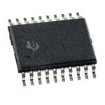
| 供应商器件封装 | 20-HTSSOP |
| 关闭 | Shutdown |
| 其它名称 | 296-24678-2 |
| 包装 | 带卷 (TR) |
| 单位重量 | 81.800 mg |
| 同步整流器 | 是 |
| 商标 | Texas Instruments |
| 安装类型 | 表面贴装 |
| 安装风格 | SMD/SMT |
| 封装 | Reel |
| 封装/外壳 | 20-TSSOP(0.173",4.40mm 宽)裸焊盘 |
| 封装/箱体 | HTSSOP-20 |
| 工作温度 | -40°C ~ 125°C |
| 工作温度范围 | - 40 C to + 125 C |
| 工厂包装数量 | 2000 |
| 开关频率 | 440 kHz |
| 拓扑结构 | Boost, Buck |
| 最大工作温度 | + 125 C |
| 最大输入电压 | 40 V |
| 最小工作温度 | - 40 C |
| 最小输入电压 | 1.5 V |
| 标准包装 | 2,000 |
| 电压-输入 | 1.5 V ~ 40 V |
| 电压-输出 | 5V |
| 电流-输出 | 500mA |
| 电源电压-最小 | 1.5 V |
| 电源电流 | 100 uA |
| 类型 | 降压(降压),升压(升压) |
| 系列 | TPS55065-Q1 |
| 输入电压 | 1.5 V to 40 V |
| 输出数 | 1 |
| 输出电压 | 5 V |
| 输出电流 | 0.5 A |
| 输出端数量 | 1 Output |
| 输出类型 | 固定 |
| 配用 | /product-detail/zh/TPS55065EVM/296-31209-ND/2262033 |
| 频率-开关 | 440kHz |


- 商务部:美国ITC正式对集成电路等产品启动337调查
- 曝三星4nm工艺存在良率问题 高通将骁龙8 Gen1或转产台积电
- 太阳诱电将投资9.5亿元在常州建新厂生产MLCC 预计2023年完工
- 英特尔发布欧洲新工厂建设计划 深化IDM 2.0 战略
- 台积电先进制程称霸业界 有大客户加持明年业绩稳了
- 达到5530亿美元!SIA预计今年全球半导体销售额将创下新高
- 英特尔拟将自动驾驶子公司Mobileye上市 估值或超500亿美元
- 三星加码芯片和SET,合并消费电子和移动部门,撤换高东真等 CEO
- 三星电子宣布重大人事变动 还合并消费电子和移动部门
- 海关总署:前11个月进口集成电路产品价值2.52万亿元 增长14.8%


PDF Datasheet 数据手册内容提取
Product Sample & Technical Tools & Support & Folder Buy Documents Software Community TPS55065-Q1 SLIS132A–OCTOBER2008–REVISEDMARCH2015 TPS55065-Q1 Buck and Boost Switched-Mode Regulator 1 Features 3 Description • QualifiedforAutomotiveApplications The TPS55065 is a switched-mode regulator with 1 integratedswitchesforvoltage-modecontrol.Withthe • AEC-Q100QualifiedWiththeFollowingResults aid of external components (LC combination), the – DeviceTemperatureGrade1: –40°Cto device regulates the output to 5 V ±3% for a wide +125°CAmbientOperatingTemperature input-voltagerange. Range The TPS55065 device offers a reset function to – DeviceHBMESDClassificationLevel1B detectandindicatewhenthe5-Voutputrailisoutside – DeviceCDMESDClassificationLevelC4B of the specified tolerance. This reset delay is programmable using an external timing capacitor on • Switched-ModeRegulator the REST terminal. Additionally, an alarm (A ) OUT – 5V±2%,NormalMode feature is activated when the input supply rail V is driver – 5V±3%,Low-PowerorCrossoverMode below a prescaled specified value (set by the A IN terminal). • SwitchingFrequency,440kHz(Typical) • InputOperatingRange,1.5Vto40V,(V ) The TPS55065 device has a frequency-modulation driver scheme to minimize EMI. The clock modulator – 500-mALoad-CurrentCapability permits a modulation of the switching frequency to – 200-mALoad-CurrentCapabilityDownto2-V reduceinterferenceenergyinthefrequencyband. Input(V ) driver The 5-Vg output is a switched 5-V regulated output – 120-mALoad-CurrentCapabilityDownto with internal current limiting to prevent assertion of 1.5-VInput(V ) driver RESET when powering a capacitive load on the • EnableFunction supply line. This function is controlled by the • Low-PowerOperationMode 5Vg_ENABLE terminal. If there is a short to ground on this output (5Vg output), the output self-protects • Switched5-VRegulatedOutputon5VgWith by operating in a chopping mode. This does, CurrentLimit however, increase the output ripple voltage on V OUT • ProgrammableSlewRateandFrequency duringthisfaultcondition. ModulationforEMIConsideration DeviceInformation(1) • ResetFunctionWithDeglitchTimerand ProgrammableDelay PARTNUMBER PACKAGE BODYSIZE(NOM) • AlarmFunctionforUndervoltageDetectionand TPS55065-Q1 HTSSOP(20) 6.50mmx4.40mm Indication (1) For all available packages, see the orderable addendum at theendofthedatasheet. • ThermallyEnhancedPackageforEfficientHeat Management SimplifiedSchematic 2 Applications Cboot1 External Schottky • AutomotiveInfotainmentandCluster Vbattery L Vdriver Vreg Osc CPhuamrgpe Q1 L1 4.7 nFDiodeM R@aexq .1@ u02i.r 541eº dCAV, Q2 • 12-VIndustrialPowerSystems R2 C ENAVBloLgiEc CSoDwnetirtacodhlle-TMri m oWdeeith Q3 LC2boot24.21720 n0mFmHH– • Servers 470 nF Bandgap AIN Ref Q4 VOUT 5 V Supply R1 12 kWRmod MoCdlouclaktor -+- Vref CPInhuramursgphe PGND 22 µF–470 µF 5Vg_ENABLE + Current Limit + 5Vg 5Vg_Supply - 1 µF–100 µF SSCCRR01 SlCeown Rtroalte SRheugtudloawtonr MToenmitpor AOU5T kW Low-DPiogwitaelr SMigondael CLP LoCwMo-oPndtoreowler BanRdegfap DPeOlaRy TWimither 5 kW GND RESET REST 2.2 nF–150 nF B0130-01 Allcomponentvaluesaretypical. 1 An IMPORTANT NOTICE at the end of this data sheet addresses availability, warranty, changes, use in safety-critical applications, intellectualpropertymattersandotherimportantdisclaimers.PRODUCTIONDATA.
TPS55065-Q1 SLIS132A–OCTOBER2008–REVISEDMARCH2015 www.ti.com Table of Contents 1 Features.................................................................. 1 7.2 FunctionalBlockDiagram.......................................11 2 Applications........................................................... 1 7.3 FeatureDescription.................................................12 3 Description............................................................. 1 7.4 DeviceFunctionalModes........................................15 4 RevisionHistory..................................................... 2 8 ApplicationandImplementation........................ 18 8.1 ApplicationInformation ..........................................18 5 PinConfigurationandFunctions......................... 3 8.2 TypicalApplication..................................................18 6 Specifications......................................................... 4 9 PowerSupplyRecommendations...................... 20 6.1 AbsoluteMaximumRatings......................................4 10 Layout................................................................... 20 6.2 ESDRatings..............................................................4 6.3 RecommendedOperatingConditions.......................4 10.1 LayoutGuidelines.................................................20 6.4 ThermalInformation..................................................5 10.2 LayoutExample....................................................21 6.5 DissipationRatings...................................................5 11 DeviceandDocumentationSupport................. 24 6.6 ElectricalCharacteristics...........................................6 11.1 DocumentationSupport .......................................24 6.7 SwitchingCharacteristics..........................................7 11.2 Trademarks...........................................................24 6.8 TypicalCharacteristics..............................................8 11.3 ElectrostaticDischargeCaution............................24 7 DetailedDescription............................................ 11 11.4 Glossary................................................................24 7.1 Overview.................................................................11 12 Mechanical,Packaging,andOrderable Information........................................................... 24 4 Revision History ChangesfromOriginal(October2008)toRevisionA Page • AddedESDRatingstable,FeatureDescriptionsection,DeviceFunctionalModes,ApplicationandImplementation section,PowerSupplyRecommendationssection,Layoutsection,DeviceandDocumentationSupportsection,and Mechanical,Packaging,andOrderableInformationsection ................................................................................................. 4 2 SubmitDocumentationFeedback Copyright©2008–2015,TexasInstrumentsIncorporated ProductFolderLinks:TPS55065-Q1
TPS55065-Q1 www.ti.com SLIS132A–OCTOBER2008–REVISEDMARCH2015 5 Pin Configuration and Functions PWPHTSSOPPackage 20Pins TopView SCR1 1 20 SCR0 Cboot2 2 19 5Vg_ENABLE Cboot1 3 18 ENABLE Vdriver 4 17 Vlogic L1 5 16 GND PGND 6 15 R mod L2 7 14 REST VOUT 8 13 AOUT 5Vg 9 12 RESET A 10 11 CLP IN PinFunctions PIN I/O DESCRIPTION NAME NO. SCR1 1 I Programmableslew-ratecontrol Cboot2 2 I Externalbootstrapcapacitor Cboot1 3 I Externalbootstrapcapacitor V 4 I Inputvoltagesource driver L1 5 I Inductorinput(anexternalSchottkydiode(1)toGNDmustbeconnectedtoL1) PGND 6 I Powerground L2 7 I Inductoroutput V 8 O 5-Vregulatedoutput OUT 5Vg 9 O Switched5-Vsupply A 10 I Programmablealarmsetting IN CLP 11 I/O Low-poweroperationmode(digitalinput) RESET 12 O Resetfunction(opendrain) A 13 O Alarmoutput(opendrain) OUT REST 14 O Programmableresettimerdelay R 15 I MainswitchingfrequencymodulationsettingtominimizeEMI mod GND 16 I Ground V 17 O Supplydecouplingoutput(maybeusedasa5-Vsupplyforlogic-levelinputs) logic ENABLE 18 I Switched-moderegulatorenable/disable 5Vg_ENABLE 19 I Switched5-Vvoltageregulatoroutputenable/disable SCR0 20 I Programmableslew-ratecontrol Exposed — — ConnecttoGNDorleftfloating. thermalpad (1) Maximum0.4Vat1Aat125°C Copyright©2008–2015,TexasInstrumentsIncorporated SubmitDocumentationFeedback 3 ProductFolderLinks:TPS55065-Q1
TPS55065-Q1 SLIS132A–OCTOBER2008–REVISEDMARCH2015 www.ti.com 6 Specifications 6.1 Absolute Maximum Ratings overoperatingfree-airtemperaturerange(unlessotherwisenoted) (1) MIN MAX UNIT V (2) Unregulatedinputvoltage, –0.5 40 V (driver) V ,V (2) Unregulatedinputs –0.5 40 V (AIN) (ENABLE) V Bootstrapvoltages 52 V (Cboot1) V 14 V (Cboot2) V Switchmodevoltages –1 40 V (L1) V –1 7 V (L2) V ,V ,V , Logicinputvoltages –0.5 7 V (Rmod) (SCR0) (SCR1) V ,and (CLP) V (2) (5Vg_ENABLE) V ,V ,V , Lowoutputvoltages –0.5 7 V (RESET) (AOUT) (logic) andV (2) (REST) P Continuouspowerdissipation SeeDissipationRatings D T Operatingvirtualjunctiontemperature –40 150 °C J T Operatingambienttemperature –40 125 °C A T Storagetemperature –65 125 °C stg (1) StressesbeyondthoselistedunderAbsoluteMaximumRatingsmaycausepermanentdamagetothedevice.Thesearestressratings only,whichdonotimplyfunctionaloperationofthedeviceattheseoranyotherconditionsbeyondthoseindicatedunderRecommended OperatingConditions.Exposuretoabsolute-maximum-ratedconditionsforextendedperiodsmayaffectdevicereliability. (2) Allvoltagevaluesarewithrespecttoground. 6.2 ESD Ratings VALUE UNIT Classification1Bforpin7,pin8, ±800 Humanbodymodel(HBM),perAEC pin9 Q100-002(1)(2) Classification2forpins1to6and ±2000 V Electrostaticdischarge V (ESD) 10to20 Chargeddevicemodel(CDM),per ClassificationLevelC4BforAll ±750 AECQ100-011 pins (1) AECQ100-002indicatesHBMstressingisdoneinaccordancewiththeANSI/ESDA/JEDECJS-001specification. (2) Thehumanbodymodelisa100-pFcapacitordischargedthrougha1.5-kΩresistorintoeachterminal. 6.3 Recommended Operating Conditions MIN NOM MAX UNIT Unregulatedinputvoltage,V 6 24 V (driver) Unregulatedinputvoltages,V andV 0 24 V (AIN) (ENABLE) V –1 17 (L1) Switched-modeterminals V V 5 5.5 (L2) V V +10 (Cboot1) (driver) Bootstrapvoltages V V 8 (Cboot2) Logiclevels(I/O),V ,V ,V ,V ,V ,V ,V , (Rmod) (logic) (SCR0) (SCR1) (5Vg_ENABLE) (RESET) (AOUT) 0 5.25 V V ,andV (CLP) (REST) Operatingambienttemperaturerange,T –40 125 °C A Logiclevels(I/O),V ,V ,V directlyconnectedtoV V V V (SCR0) (SCR1) (CLP) (logic) (logic) (logic) 4 SubmitDocumentationFeedback Copyright©2008–2015,TexasInstrumentsIncorporated ProductFolderLinks:TPS55065-Q1
TPS55065-Q1 www.ti.com SLIS132A–OCTOBER2008–REVISEDMARCH2015 6.4 Thermal Information TPS55065-Q1 THERMALMETRIC(1) PWP[HTSSOP] UNIT 20PINS R Junction-to-ambientthermalresistance 37.9 θJA R Junction-to-case(top)thermalresistance 22.7 θJC(top) R Junction-to-boardthermalresistance 20.2 θJB °C/W ψ Junction-to-topcharacterizationparameter 0.7 JT ψ Junction-to-boardcharacterizationparameter 19.9 JB R Junction-to-case(bottom)thermalresistance 1.8 θJC(bot) (1) Formoreinformationabouttraditionalandnewthermalmetrics,seetheICPackageThermalMetricsapplicationreport,SPRA953. 6.5 Dissipation Ratings POWERRATING DERATINGFACTORABOVE POWERRATING POWERRATING R θJA T ≤25°C T =25°C T =85°C T =125°C A A A A 32°C/W 3.9W 31.25mW/°C 2.03W 0.781W 40°C/W 3.125W 25mW/°C 1.625W 0.625W Copyright©2008–2015,TexasInstrumentsIncorporated SubmitDocumentationFeedback 5 ProductFolderLinks:TPS55065-Q1
TPS55065-Q1 SLIS132A–OCTOBER2008–REVISEDMARCH2015 www.ti.com 6.6 Electrical Characteristics V =6Vto17V,T =-40°Cto125°C,unlessotherwisenoted (driver) A PARAMETER TESTCONDITIONS MIN TYP MAX UNIT V Unregulatedinputvoltage 1.5 40 V (driver) V Start-upconditionvoltage I =500mA 5 V (driver) O C =36μF(minimum)to220μF O 4 20 (maximum) S Soft-startramp V/ms OM C =220μF(min)to470μF(max),see NOote (1) 2 20 I Standbycurrent ENABLE=low 10 20 μA (standby) I Quiescentcurrent CLP=0V,V =11V,I =0mA 100 160 μA q (driver) O V Outputvoltage DC 5 V O Normalmode 2% V Output-voltagetolerance O Boost/buckcrossoverorlow-powermode 3% I Outputcurrent V ≥7V 0.5 A O (driver) V =2V,seeNote (2) 200 (driver) I Outputcurrent,boostmode mA O(Boost) V =1.5V,seeNote (2) 120 (driver) I Internalpeakcurrentlimit(normal See (1) 1.75 2.5 A PPn mode) I Internalpeakcurrentlimit(low- See (1) 0.75 1.25 A PPl powermode) I Peakcurrent V =16V,I =500mA,L=33μH 1.5 A P (driver) O V Boost/buckcrossovervoltage See (3) 5 5.9 V (driver) window T Thermalshutdown(4) 160 180 200 °C ot 5VgOUTPUTANDENABLE r On-stateresistance 135 225 mΩ DS(on) I Outputcurrent 400 mA O V 5Vg_ENABLEinput-voltagerange –0.5 V V I O 5Vg_ENABLEthresholdhigh V V =5V 2.5 3 3.5 V IH voltage (5Vg) 5Vg_ENABLEthresholdlow V V =0V 1.5 2 2.5 V IL voltage (5Vg) V Hysteresisvoltage 0.5 1 V (hys) r Internalpulldownresistor 300 500 850 kΩ (pd) ENABLE V ENABLEinput-voltagerange –0.5 40 V I 8V≤V ≤17V 2.5 3 3.5 (driver) V ENABLEthresholdhighvoltage V IH 6V≤V <8V 1.9 3 3.5 (driver) V ENABLEthresholdlowvoltage V =5V 1.5 2 2.5 V IL O 8V≤V ≤17V 0.5 1 (driver) V Hysteresisvoltage V (hys) 6V≤V <8V 0.1 (driver) (1) Ensuredbycharacterization. (2) Testedwithinductorhavingfollowingcharacteristics:L=33μH,R =0.1Ω,I =1.8A.Outputcurrentmustbeverifiedinapplication max R wheninductorR (ESR)isincreased. max (3) Ensuredbycharacterization.Forfurtherdetails,seeBuck/BoostTransitioning. (4) Ensuredbycharacterization;hysteresis15°C(typical) 6 SubmitDocumentationFeedback Copyright©2008–2015,TexasInstrumentsIncorporated ProductFolderLinks:TPS55065-Q1
TPS55065-Q1 www.ti.com SLIS132A–OCTOBER2008–REVISEDMARCH2015 Electrical Characteristics (continued) V =6Vto17V,T =-40°Cto125°C,unlessotherwisenoted (driver) A PARAMETER TESTCONDITIONS MIN TYP MAX UNIT RESET V RESETthresholdvoltage 4.51 4.65 4.79 V (th) V RESETtolerance 3% (RESET) C =10nF 8 10 12 (REST) t RESETtime ms (RESET) C =100nF,see (1) 80 100 120 (REST) I =5mA 450 sink V RESEToutputlowvoltage mV OL I =1mA 84 sink t RESETdeglitchtime See (1) 8 10 12.5 μs (deglitch) ALARM V Alarminput-voltagerange –0.5 40 V I V Alarmthresholdlowvoltage 2.2 2.3 2.35 V IL V Alarmthresholdhighvoltage 2.43 2.5 2.58 V IH V Hysteresisvoltage 200 mV (hys) I =5mA 450 sink V Alarmoutputlowvoltage mV OL I =1mA 84 sink LOW-POWERMODE(PULSEMODE)PFM I Loadcurrentinlow-powermode V <7V 50 mA O(LPM) (driver) I Averageinputcurrent V =11V,I =5mA,CLP=low 3.55 mA I(avg) (driver) O V Output-voltagetolerance V =5V 2.4% 3% O O DIGITALLOW-POWERMODE(CLP) High-levelCLPinputthreshold V Normalmode 2.6 V IH voltage Low-levelCLPinputthreshold V Low-powermode 1.15 V IL voltage 6.7 Switching Characteristics overoperatingfree-airtemperaturerange(unlessotherwisenoted) PARAMETER TESTCONDITIONS MIN TYP MAX UNIT f Switchingfrequency V =0V,modulatorOFF 440 kHz (sw) (Rmod) f Operating-frequencyaccuracy f =440kHz 20% (sw)ac (sw) f Modulationminimumfrequency 270 330 445 kHz (sw)min f Modulationmaximumfrequency 450 550 680 kHz (sw)max f Modulationspan 220 kHz (mod)span f Modulationfrequency R =12kΩ±1% 28 kHz (mod) mod f Modulation-frequencyaccuracy 12% (mod)ac Copyright©2008–2015,TexasInstrumentsIncorporated SubmitDocumentationFeedback 7 ProductFolderLinks:TPS55065-Q1
TPS55065-Q1 SLIS132A–OCTOBER2008–REVISEDMARCH2015 www.ti.com 6.8 Typical Characteristics (ReferenceL1Terminal,seeFigure8throughFigure10) 6 1.0 V(driver) = 11 V 0.9 V(driver)= 11V 5 0.8 I − Input Current − mAI 234 TA = 125° Maximum TA = 25° I- Input Current - mAI 00000.....34567 TA= 125° Maximum TA= 25° 0.2 1 0.1 0 0.0 0 1 2 3 4 5 6 7 8 9 10 0.0 0.1 0.2 0.3 0.4 0.5 0.6 0.7 0.8 0.9 1.0 IO − Output Current − mA G001 IO- Output Current - mA G002 Maximumcharacteristicspecifiedbydesign. Maximumcharacteristicspecifiedbydesign. Figure1.Low-PowerModeCurrent,I =0mA–10mA Figure2.Low-Power-ModeCurrent,I =0mA–1mA O O V(L1) Input Current (200 mA/div) G005 G010 Figure3.InputCurrentwithSlopeControl,SCR0=0, Figure4.InputCurrentwithSlopeControl,SCR1=0, SCR1=0,Input-CurrentSlewRate=2.8A/µs,I =500mA, SCR0=1,Input-CurrentSlewRate=6.25A/µs, L V =15V I =500mA,V =15V (driver) L (driver) G011 G008 Figure5.InputCurrentwithSlopeControl,SCR1=1,SCR0 Figure6.InputCurrentWithSlopeControl,SCR0=1,SCR1 =0,Input-CurrentSlewRate=9.4A/µs,I =500mA,V =1,Input-CurrentSlewRate=18.8A/µs,I =500mA, L (driver) L =15V V =15V (driver) 8 SubmitDocumentationFeedback Copyright©2008–2015,TexasInstrumentsIncorporated ProductFolderLinks:TPS55065-Q1
TPS55065-Q1 www.ti.com SLIS132A–OCTOBER2008–REVISEDMARCH2015 Typical Characteristics (continued) (ReferenceL1Terminal,seeFigure8throughFigure10) G009 G013 Figure7.Low-Power-ModeOperation,I =15mA, Figure8.MinimumSwitchingFrequency(333kHz) L CO=47µF withModulationEnabled,Rmod=12kΩ,IL=200mA G006 G007 Figure9.MaximumSwitchingFrequency(555kHz) Figure10.ModulationFrequency(FullSpan)of28kHz WithModulationEnabled,R =12kΩ,I =200mA mod L VO 11 V, IL= 500 mA V(driver) 5 V, IL= 500 mA 2 V, IL= 225 mA G015 Figure11.InputVoltageExcursions(SimilartoLow-Crank Figure12.Switched-ModeRegulatorTransitionfromBuck Conditions) ModetoBoostMode,I =400mA L Copyright©2008–2015,TexasInstrumentsIncorporated SubmitDocumentationFeedback 9 ProductFolderLinks:TPS55065-Q1
TPS55065-Q1 SLIS132A–OCTOBER2008–REVISEDMARCH2015 www.ti.com Typical Characteristics (continued) (ReferenceL1Terminal,seeFigure8throughFigure10) G012 G016 Figure13.NominalSwitchingFrequencyofQ1Switch Figure14.Switched-ModeRegulatorTransitionfromBoost (446kHz)WithModulationFunctionDisabled,IL=200mA ModetoBuckMode,IL=400mA Modulation Off Modulation = 28 kHz B/div B/div Slew Rate = 11 10d 10d Slew Rate = 00 G G O O L L G017 G018 ThesevaluesrepresentconductedEMIresultsofatestboardfor ThesevaluesrepresentconductedEMIresultsofatestboardfor displaypurposesonly.Actualresultsmayvarygreatlydepending displaypurposesonly.Actualresultsmayvarygreatlydepending onboardlayoutandexternalcomponentsandmustbeverifiedin onboardlayoutandexternalcomponentsandmustbeverifiedin actualapplication. actualapplication. Figure15.ConductedEmissionsonTestBoardShowing Figure16.ConductedEmissionsonTestBoardShowing EffectsofSwitching-FrequencyModulation EffectsofMinimumandMaximumSlewRateSettings 10 SubmitDocumentationFeedback Copyright©2008–2015,TexasInstrumentsIncorporated ProductFolderLinks:TPS55065-Q1
TPS55065-Q1 www.ti.com SLIS132A–OCTOBER2008–REVISEDMARCH2015 7 Detailed Description 7.1 Overview The TPS55065 is a buck/boost switched-mode regulator that operates in a power-supply concept to ensure a stableoutputvoltagewithinputvoltageexcursionsandspecifiedloadrange. The device provides an alarm indicator and reset output to interface with systems that require supervisory function. The switching regulator offers a clock modulator and a current-mode slew-rate control for the internal switching transistor(Q1)tominimizeEMI. An internal low-r switch has a current-limit feature to prevent inadvertent reset when turning on the 5-Vg DS(on) output. 7.2 Functional Block Diagram Cboot1 External Schottky Diode Required, Q1 4.7 nF Max. 0.4 V L Vdriver Charge @ 1@2 51ºCA Vbattery Vreg Osc Pump L1 Q2 22mH– C 100mH L2 ENABLE Switch-Mode 4.7 nF R2 Vlogic Controller With Q3 DeadTime Cboot2 470 nF Bandgap Ref AIN Q4 VOUT 5 V Supply R R1 mod Clock - PGND 22 µF–470 µF Modulator + Vref Charge Pump 12 kW - Inrush 5Vg_ENABLE + Current Limit 5 + Vg 5Vg_Supply - 1 µF–100 µF SCR0 A Slew Rate Shutdown OUT SCR1 Control Regulator Temp 5 kW Monitor CLP Low-Power Low-Power Mode Mode Bandgap POR With 5 kW Digital Signal Control Ref DelayTimer GND RESET REST 2.2 nF–150 nF B0130-01 Allcomponentvaluesaretypical. Copyright©2008–2015,TexasInstrumentsIncorporated SubmitDocumentationFeedback 11 ProductFolderLinks:TPS55065-Q1
TPS55065-Q1 SLIS132A–OCTOBER2008–REVISEDMARCH2015 www.ti.com 7.3 Feature Description 7.3.1 Switched-ModeInput/OutputTerminals(L1,L2) Theexternalinductorfortheswitched-moderegulatorisconnectedbetweenterminalsL1andL2.Thisinductoris placedclosetotheterminalstominimizeparasiticeffects.Forstability,useaninductorwith20 μHto100μH. 7.3.2 SupplyTerminal(V ) driver The input voltage of the device is connected to the V terminal. This input line requires a filter capacitor to driver minimize noise. TI recommends using a low-ESR aluminum or tantalum input capacitor. The relevant parameters for the input capacitor are the voltage rating and RMS current rating. The voltage rating should be approximately 1.5 times the maximum applied voltage for an aluminum capacitor and 2 times for a tantalum capacitor. In buck mode, the RMS current is IOUT(cid:1)(cid:3)D(cid:2)D2, where D is the duty cycle and its maximum RMS current value is reached when D = 50% with I = I /2. In boost mode, the RMS current is 0.3 × ΔI, where ΔI is the peak-to- RMS OUT peak ripple current in the inductor. To achieve this, ESR ceramic capacitors are used in parallel with the aluminumortantalumcapacitors. 7.3.3 InternalSupplyDecouplingTerminal(V ) logic The V terminal is used to decouple the internal power-supply noise by use of a 470-nF capacitor. This logic terminal can also be used as an output supply for the logic-level inputs for this device (SCR0, SCR1, ENABLE, CLP,and5Vg_ENABLE). 7.3.4 InputVoltageMonitoringTerminal(A ) IN The A terminal is used to program the threshold voltage for monitoring and detecting undervoltage conditions IN on the input supply. A maximum of 40 V may be applied to this terminal and the voltage at this terminal may exceed the V input voltage without effecting the device operation. The resistor divider network is (driver) programmed to set the undervoltage detection threshold on this terminal (see the application schematic). The input has a typical hysteresis of 200 mV with a typical upper limit threshold of 2.5 V and a typical lower limit threshold of 2.3 V. When V falls below 2.3 V, V is asserted low; when V exceeds 2.5 V, V is in (AIN) (AOUT) (AIN) (AOUT) thehigh-impedancestate. TheequationstosettheupperandlowerthresholdsofV are: (AIN) . Upper: R1 + R2 V = 2.5 V × (driver) R1 Lower: R1 + R2 V = 2.3 V × (driver) R1 (1) 7.3.5 InputUndervoltageAlarmTerminal(A ) OUT The A terminal is an open-drain output that asserts low when the input voltage falls below the set threshold OUT ontheA input. IN 7.3.6 ResetDelayTimerTerminal(REST) The REST terminal sets the desired delay time to assert the RESET terminal low after the 5-V supply has exceeded 4.65 V (typical). The delay can be programmed in the range of 2.2 ms to 150 ms using capacitors in therangeof2.2nFto150nF.ThedelaytimeiscalculatedusingEquation2: RESETdelay=C ×1ms (REST) whereC hasnFunits. (2) (REST) 7.3.7 ResetTerminal(RESET) The RESET terminal is an open-drain output. The power-on reset output is asserted low until the output voltage exceedsthe4.65-Vthresholdandtheresetdelaytimerhasexpired.Additionally,whenevertheENABLEterminal islow,RESETisimmediatelyassertedlowregardlessoftheoutputvoltage. 12 SubmitDocumentationFeedback Copyright©2008–2015,TexasInstrumentsIncorporated ProductFolderLinks:TPS55065-Q1
TPS55065-Q1 www.ti.com SLIS132A–OCTOBER2008–REVISEDMARCH2015 Feature Description (continued) 7.3.8 MainRegulatorOutputTerminal(V ) OUT The V terminal is the output of the switched-mode regulated supply. This terminal requires a filter capacitor OUT with low-ESR characteristics to minimize output ripple voltage. For stability, a capacitor with 22 μF to 470 μF shouldbeused.ThetotalcapacitanceatpinV andpin5Vgmustbelessthanorequalto470 μF. OUT 7.3.9 Low-Power-ModeTerminal(CLP) The CLP terminal controls the low-power mode of the device. An external low digital signal switches the device tolow-powermodeornormalmodewhentheinputishigh. 7.3.10 Switch-OutputTerminal(5Vg) The 5Vg terminal switches the 5-V regulated output. The output voltage of the regulator can be enabled or disabledusingthislow-r internalswitch.Thisswitchhasacurrent-limitingfunctiontopreventgenerationofa DS(on) reset signal at turnon caused by the capacitive load on the output or overload condition. When the switch is enabled, the regulated output may deviate and drop momentarily to a tolerance of 7% until the 5Vg capacitor is fullycharged.ThisdeviationdependsonthecharacteristicsofthecapacitorsonV and5Vg. OUT 7.3.11 5Vg-EnableTerminal(5Vg_ENABLE) The5Vg_ENABLEisalogic-levelinputforenablingtheswitchoutputon5Vg. Forthefunctionalterminal,see5Vg_ENABLEresultsinTable1: Table1. 5Vg_ENABLEFunction 5Vg_ENABLE Function 0 5Vgisoff Open(internalpulldown=500kΩ) 5Vgisoff 1 5Vgison Copyright©2008–2015,TexasInstrumentsIncorporated SubmitDocumentationFeedback 13 ProductFolderLinks:TPS55065-Q1
TPS55065-Q1 SLIS132A–OCTOBER2008–REVISEDMARCH2015 www.ti.com V driver Q1 Peak Current Limit Switch Control Slew Rate Control 33 µH Q4 L1 L2 Buck/Boost V OUT Gate Driver Q3 47 µF Q2 Gate Driver 5 V Vg OUT 5 Charge Pump Vg typ ~V –100 mV OUT 100 µF RESET V OUT typ 4.65 V RESETDeglitch RESET 5Vg_ENABLE S0174-01 Figure17. Current-LimitSwitchedOutput5Vg 7.3.12 Slew-RateControlTerminals(SCR0,SCR1) TheslewrateoftheswitchingtransistorQ1issetusingtheSCR0andSCR1terminals. Table2showsthevaluesoftheslewrate(SR): Table2.SRValues SCR1 SCR0 SR Q1 0 0 Slow 0 1 Medium-slow 1 0 Medium-fast 1 1 Fast 14 SubmitDocumentationFeedback Copyright©2008–2015,TexasInstrumentsIncorporated ProductFolderLinks:TPS55065-Q1
TPS55065-Q1 www.ti.com SLIS132A–OCTOBER2008–REVISEDMARCH2015 Seetheconverterefficiencyplotsinthe TypicalCharacteristicssectiontodeterminepowerdissipation. 7.3.13 ModulatorFrequencySetting(TerminalR ) mod The R terminal adjusts the clock modulator frequency. A resistor of R = 12 kΩ generates a modulation mod mod frequency of 28 kHz. The modulator function may be disabled by connecting R to GND and the device mod operates with the nominal frequency. The modulator function cannot be activated during IC operation, only at IC start-up. 7.3.14 GroundTerminal(PGND) ThePGNDterminalisthepowergroundforthedevice. 7.3.15 EnableTerminal(ENABLE) The ENABLE terminal allows the enabling and disabling of the switch mode regulator. A maximum of 40 V may be applied to this terminal to enable the device and increasing it above the V input voltage does not affect (driver) thedeviceoperation. ThefunctionalityoftheENABLEterminalisdescribedinTable3: Table3.ENABLEFunction ENABLE Function 0 Vregisoff Open Undefined 1 Vregison 7.3.16 BootstrapTerminals(CBOOT1andCBOOT2) An external bootstrap capacitor is required for driving the internal high-side MOSFET switch. A 4.7-nF ceramic capacitoristypicallyrequired. 7.4 Device Functional Modes 7.4.1 ClockModulator To minimize EMI issues associated with the switched-mode regulator, the device offers an integrated clock modulator. The function of the clock modulator is to modulate the switching frequency and to distribute the energyoverthewaveband. The average switching frequency is 440 kHz (typical) and varies between 330 kHz and 550 kHz at a rate set by the R resistor. A typical value of 12 kΩ on the R terminal relates to a 28-kHz modulation frequency. The mod mod clockmodulatorfunctioncanonlybeactivatedduringICstart-up,notduringICoperation. Theequationforthemodulationfrequencyisasfollows: f (Hz)=(–2.2×R )+54.5kHz (mod) mod whenR =8kΩto16kΩ. (3) mod 7.4.2 Buck/BoostTransitioning The operation mode switches automatically between buck and boost modes depending on the input voltage of V and output load conditions. During start up, when V is less than 5.8 V (typical), the device starts in (driver) (driver) boost mode and continues to run in boost mode until V exceeds 5.8 V; at which time, the device switches (driver) over to buck mode. In buck mode, the device continues to run in buck mode until it is required to switch back to boost to hold regulation. This crossover window to switch to boost mode is when V is between 5.8 V and (driver) 5 V and depends on the loading conditions. When V drops below 5.8 V but the device is holding regulation driver (~2%), the device remains in buck mode. However, when V is within the 5.8-V to 5-V window and V (driver) OUT drops to 4.9 V, the device crosses over to boost mode to hold regulation. In boost mode, the device remains in Copyright©2008–2015,TexasInstrumentsIncorporated SubmitDocumentationFeedback 15 ProductFolderLinks:TPS55065-Q1
TPS55065-Q1 SLIS132A–OCTOBER2008–REVISEDMARCH2015 www.ti.com Device Functional Modes (continued) boost mode until V exceeds 5.8 V; at which time, the device enters the buck mode. When the device is (driver) operatinginboostmodeandV isinthecrossoverwindowof5.8Vto5V,theoutputregulationmaycontain (driver) a higher than normal ripple and only maintain a 3% tolerance. This ripple and tolerance depends on the loading and improves with a higher loading condition. When the device is operated with low-power mode active (CLP = low)andhighoutputcurrents(>50mA),thebuck/boosttransitioningcancausearesetsignalattheRESETpin. 7.4.3 BuckSMPS In buck mode, the duty cycle of transistor Q1 sets the voltage V . The duty cycle of transistor Q1 varies 10% OUT to 99% depending on the input voltage, V . If the peak inductor current (measured by Q1) exceeds 450 mA (driver) (typical),Q2isturnedonforthiscycle(synchronizedrectification).Otherwise,thecurrentrecirculatesthroughQ2 asafree-wheelingdiode.Thedetectionforsynchronousorasynchronousmodeisdonecycle-by-cycle. To avoid a cross-conduction current between Q1 and Q2, an inherent delay is incorporated when switching Q1 offandQ2onandviceversa. In buck mode, transistor Q3 is not required and is switched off. Transistor Q4 is switched on to reduce power dissipation. The switch timings for transistors Q3 and Q4 are not considered. In buck mode, the logical control of the transistorsdoesnotchange. Input Vdriver Voltage SMPS Q1 Current Control L1 Q2 Switch 33 µH Control L2 Q4 V OUT Q3 22 µF–470 µF FB S0182-01 Figure18. Buck/BoostSwitchModeConfiguration 7.4.4 BoostSMPS In boost mode, the duty cycle of transistor Q3 controls the output voltage V . The duty cycle is internally OUT adjusted 5% to 85% depending on the internally sensed voltage of the output. Synchronized rectification occurs whenV isbelow5V. (driver) To avoid a discharging of the buffer capacitor, a simultaneous switching on of Q3 and Q4 is not allowed. An inherentdelayisincorporatedbetweenQ3switchingoffandQ4switchingonandviceversa. In boost mode, transistor Q2 is not required and remains off. Transistor Q1 is switched on for the duration of the boost-modeoperation(servesasasupplyline). 16 SubmitDocumentationFeedback Copyright©2008–2015,TexasInstrumentsIncorporated ProductFolderLinks:TPS55065-Q1
TPS55065-Q1 www.ti.com SLIS132A–OCTOBER2008–REVISEDMARCH2015 Device Functional Modes (continued) The switch timings of transistors Q1 and Q2 are not considered. In boost mode, the logical control of the transistorsdoesnotchange. 7.4.5 ExtensionoftheInputVoltageRangeonV (driver) To ensure a stable 5-V output voltage with the output load in the specified range, the V supply must be (driver) greater than or equal to 5 V for greater than 1 ms (typical). After a period of 1 ms (typical), the logic may be suppliedbytheV regulatorandtheV supplymaybecapableofoperatingdownto1.5V. OUT (driver) Theswitched-moderegulatordoesnotstartatV lessthan5V. (driver) 7.4.6 Low-PowerMode Toreducequiescentcurrentandtoprovideefficientoperation,theregulatorentersapulsedmode. Thedeviceentersthismodebyalogic-levellowonthisterminal. Automatic low-power mode is not available. The low-power-mode function is not available in boost mode. The deviceleaveslow-powermodeduringboostmoderegardlessofthelogiclevelontheCLPterminal. 7.4.7 TemperatureandShort-CircuitProtection To prevent thermal destruction, the device offers overtemperature protection to disable the IC. Also, short-circuit protectionisincludedforaddedprotectiononV and5Vg. OUT 7.4.8 SwitchOutputTerminal(5Vg)CurrentLimitation A charge pump drives the internal FET, which switches the primary output voltage V to the 5Vg pin. OUT Protection is implemented to prevent the output voltage from dropping below its specified value while enabling the secondary output voltage. An explanation of the block diagram (see Figure 1) is given by the following example: • Deviceisenabled,outputvoltageV isupandstable. OUT • 5Vgisenabled(pin5Vg_ENABLEsettohigh)withloadresistanceconnectedto5Vgpin. • If output voltage V drops below typical ( V – 100 mV), the charge pump of the 5Vg FET is switched off OUT OUT andtheFETremainsonforawhileasthegatevoltagedropsslowly. • If V drops below the RESET threshold of 4.65 V (typical), the FET of the secondary output voltage 5Vg is OUT switchedoff(gatedrawntogroundlevel). • A deglitch time ensures that a device reset does not occur if V drops to the reset level during the 5Vg OUT turnonphase. • If V rises above typical (V – 100 mV), the charge pump of the 5Vg FET is switched on and drives the OUT OUT gateofthe5VgFETon. 7.4.9 SoftStart On power up, the device offers a soft-start feature which ramps the output of the regulator at a slew of 10 V/ms. When a reset occurs, the soft start is reenabled. Additionally, if the output capacitor is greater than 220 μF (typical), the slew rate decreases to a value set by the internal current limit. In boost mode, the soft-start feature isnotactive. Copyright©2008–2015,TexasInstrumentsIncorporated SubmitDocumentationFeedback 17 ProductFolderLinks:TPS55065-Q1
TPS55065-Q1 SLIS132A–OCTOBER2008–REVISEDMARCH2015 www.ti.com 8 Application and Implementation NOTE Information in the following applications sections is not part of the TI component specification, and TI does not warrant its accuracy or completeness. TI’s customers are responsible for determining suitability of components for their purposes. Customers should validateandtesttheirdesignimplementationtoconfirmsystemfunctionality. 8.1 Application Information The TPS55065 can be operated in a buck boost configuration with voltage mode control. The device is capable of monitoring the output as well as the input supply rail. The device also offers a frequency modulation scheme for minimizing EMI. The slew rate is set using the SCR0 and the SCR1 terminals. The average converter efficiency varies with the different slew rate controls of the Q1 switching FET. These variations are demonstrated usingthisdesignexampleataninputvoltageof11Vand17V. 8.2 Typical Application 22 µH–100 µH 4.7 nF 4.7 nF L1 L2 Cboot1 V 5V OUT 22 µF–470 µF Cboot2 L Vbattery V driver C R2 5Vg 5V A IN 1 µF–100 µF R1 TPS55065 5 V ENABLE 5 kW V RESET logic 470 nF Optional 5 kW Connection A OUT 5Vg_ENABLE REST SCR1 2.2 nF–150 nF CLP SCR0 R mod 12kW PGND GND S0183-01 A. Tominimizevoltagerippleontheoutputduetotransients,itisrecommendedtousealow-ESRcapacitorontheV OUT line. B. TheLandCcomponentvaluesaresystemapplicationdependentforEMIconsideration. Figure19. ApplicationSchematic 18 SubmitDocumentationFeedback Copyright©2008–2015,TexasInstrumentsIncorporated ProductFolderLinks:TPS55065-Q1
TPS55065-Q1 www.ti.com SLIS132A–OCTOBER2008–REVISEDMARCH2015 Typical Application (continued) NOTE When this attachment method is not implemented correctly, this product may operate inefficiently. Power dissipation capability may be adversely affected when the device is incorrectlymountedontothecircuitboard. 8.2.1 DesignRequirements Forthisdesignexample,usetheparameterslistedinTable4astheinputparameters. Table4.DesignParameters DESIGNPARAMETERS VALUE InputvoltageV(driver) 11Vto18V Outputcurrent(maximum) 500mA Four different SCRx settings will be used to analyze the difference in converter efficiency with variations in slew rate(seeFigure20).TheBuckequationsmentionedinBuckMode willbeusedtocalculatetherestofthedesign parameters. 8.2.2 DetailedDesignProcedure 8.2.2.1 BuckMode • Selectinductorripplecurrent ΔI :forexample,ΔI =0.2×I L L OUT • CalculateinductorL (cid:11)V (cid:16)V (cid:12)uV L IN OUT OUT (cid:11)H(cid:12) f u'I uV SW L IN wheref istheregulatorswitchingfrequency. (4) SW • Inductorpeakcurrent 'I I I (cid:14) L (cid:11)A(cid:12) L,max OUT 2 (5) • Outputvoltageripple § 1 · (cid:11) (cid:12) 'VOUT 'ILu¨©ESR(cid:14)8ufSW uCOUT ¸¹ V(cid:11)p(cid:16)p(cid:12) (6) Usually,thefirsttermisdominant. I (cid:11)t (cid:14)t (cid:12) C pk ON OFF (cid:11)F(cid:12) OUT 8uV ripple (7) Using the previous equations, with Vin (maximum) as 18 V, Vout as 5 V, f as 440 kHz, and Inductor ripple SW currentof0.1A,theinductanceiscalculatedtobe82.1 µHwithinductorpeakcurrentas0.55A. 8.2.2.2 BoostMode • Selectinductorripplecurrent ΔI :forexampleΔI =0.2× I L L IN • CalculateinductorL (cid:11)V (cid:16)V (cid:12)uV L OUT IN IN (cid:11)H(cid:12) f u'I uV SW L OUT wheref istheregulatorswitchingfrequency. (8) SW • Inductorpeakcurrent 'I I I I (cid:14) L (cid:11)A(cid:12) P L,max IN 2 (9) Copyright©2008–2015,TexasInstrumentsIncorporated SubmitDocumentationFeedback 19 ProductFolderLinks:TPS55065-Q1
TPS55065-Q1 SLIS132A–OCTOBER2008–REVISEDMARCH2015 www.ti.com • Outputvoltageripple § V · IOUTu¨1(cid:16) IN ¸ 'V I uESR(cid:14) © VOUT ¹ (cid:11)V (cid:12) OUT P f uC (cid:11)p(cid:16)p(cid:12) SW OUT (10) 8.2.3 ApplicationCurve 85 SCR:10,V(driver)= 11V SCR:11,V(driver)= 11V 80 75 % ncy - 70 Efficie 65 SCR:10,V(driver)= 17V SCR:00,V(driver)= 17V 60 SCR:00,V(driver)= 11SVCR:01,V(driver)= 17V SCR:01,V(driver)= 11V 55 SCR:11,V(driver)= 17V 50 100 150 200 250 300 350 400 450 500 IO- Output Current - mA Figure20.ConverterEfficiency 9 Power Supply Recommendations The TPS55065-Q1 device is designed to operate from an input voltage up to 40 V. Ensure that the input supply is well regulated. Furthermore, if the supply voltage in the application is likely to reach negative voltage (for example, reverse battery), a forward diode must be placed at the input of the supply. For the V pin, a good IN quality ceramic capacitor is recommended. Capacitance de-rating for aging, temperature, and DC bias must be taken into account while determining the capacitor value. The decoupling capacitor must be as close as possible to the Input pin for proper filtering. The use of a low-ESR capacitor at the V line is recommended to minimize OUT the voltage ripple on the output due to transients. The L and C component values can be chosen as per specifications. 10 Layout 10.1 Layout Guidelines ThefollowingguidelinesarerecommendedforPCBlayoutoftheTPS55065device. 10.1.1 Inductor Use a low-EMI inductor with a ferrite-type closed core. Other types of inductors may be used; however, they musthavelow-EMIcharacteristicsandbelocatedawayfromthelow-powertracesandcomponentsinthecircuit. 10.1.2 FilterCapacitors Input ceramic filter capacitors should be located in the close proximity of the V terminal. Surface-mount driver capacitorsarerecommendedtominimizeleadlengthandreducenoisecoupling. 10.1.3 TracesandGroundPlane All power (high-current) traces should be thick and as short as possible. The inductor and output capacitors should be as close to each other as possible. This reduces EMI radiated by the power traces due to high switchingcurrents. In a two-sided PCB, it is recommended to have ground planes on both sides of the PCB to help reduce noise and ground-loop errors. The ground connection for the input and output capacitors and IC ground should be connectedtothisgroundplane. 20 SubmitDocumentationFeedback Copyright©2008–2015,TexasInstrumentsIncorporated ProductFolderLinks:TPS55065-Q1
TPS55065-Q1 www.ti.com SLIS132A–OCTOBER2008–REVISEDMARCH2015 Layout Guidelines (continued) In a multilayer PCB, the ground plane is used to separate the power plane (where high switching currents and components are placed) from the signal plane (where the feedback trace and components are) for improved performance. Also, arrange the components such that the switching-current loops curl in the same direction. Place the high- current components such that during conduction, the current path is in the same direction. This prevents magneticfieldreversalcausedbythetracesbetweenthetwohalf-cycles,helpingtoreduceradiatedEMI. 10.2 Layout Example Place switching components (L1, C1, and C2) near the device Figure21. TopLayer Copyright©2008–2015,TexasInstrumentsIncorporated SubmitDocumentationFeedback 21 ProductFolderLinks:TPS55065-Q1
TPS55065-Q1 SLIS132A–OCTOBER2008–REVISEDMARCH2015 www.ti.com Layout Example (continued) Use multiple vias to connect the input, output and package pad to the ground plane. Provide a large ground plane to reduce noise and ground-loop errors. Figure22. BottomLayer To maximize the efficiency of this package for application on a single-layer or multilayer PCB, certain guidelines mustbefollowedwhenlayingoutthisdeviceonthePCB. Thefollowinginformationistobeusedasaguidelineonly. ForfurtherinformationseethePowerPADThermallyEnhancedPackage technicalbrief(SLMA002). Thefollowingareguidelinesformountingthe PowerPAD™IConamultilayerPCBwithagroundplane. Solder Pad (Land Pattern) Package Thermal Pad Thermal Vias Package Outline M0026-01 Figure23. PackageandPCBLandConfigurationforaMultilayerPCB 22 SubmitDocumentationFeedback Copyright©2008–2015,TexasInstrumentsIncorporated ProductFolderLinks:TPS55065-Q1
TPS55065-Q1 www.ti.com SLIS132A–OCTOBER2008–REVISEDMARCH2015 Layout Example (continued) Power Pad Package Solder Pad Component Traces 1,5038-mm–1,5748-mm Component Trace (2-oz. Cu) 2 Plane 1,0142-mm–1,0502-mm Ground Plane (1-oz. Cu) Thermal Via 4 Plane 1,5748 mm 0,5246-mm–0,5606-mm Power Plane Thermal Isolation (1-oz. Cu) Power Plane Only 0-mm–0,071-mm Board Baseand Bottom Pad Package Solder Pad (Bottom Trace) M0027-01 Figure24. MultilayerBoard(SideView) In a multilayer board application, the thermal vias are the primary method of heat transfer from the package thermalpadtotheinternalgroundplane. The efficiency of this method depends on several factors (die area, number of thermal vias, thickness of copper, andsoforth).SeethePowerPADThermallyEnhancedPackage technicalbrief(SLMA002). Use as Much CopperArea as Possible for Heat Spread Package Thermal Pad Package Outline M0028-01 Figure25. LandConfigurationforSingle-LayerPCB Layout recommendation is to use as much copper area for the power-management section of a single-layer board as possible. In a single-layer board application, the thermal pad is attached to a heat spreader (copper areas)byusingalow-thermal-impedanceattachmentmethod(solderpasteorthermal-conductiveepoxy).Inboth ofthesecases,itisadvisabletouseasmuchcopperandasmanytracesaspossibletodissipatetheheat. Copyright©2008–2015,TexasInstrumentsIncorporated SubmitDocumentationFeedback 23 ProductFolderLinks:TPS55065-Q1
TPS55065-Q1 SLIS132A–OCTOBER2008–REVISEDMARCH2015 www.ti.com 11 Device and Documentation Support 11.1 Documentation Support 11.1.1 RelatedDocumentation Forrelateddocumentationseethefollowing: • PowerPADThermallyEnhancedPackage,SLMA002 11.2 Trademarks PowerPADisatrademarkofTexasInstruments. Allothertrademarksarethepropertyoftheirrespectiveowners. 11.3 Electrostatic Discharge Caution Thesedeviceshavelimitedbuilt-inESDprotection.Theleadsshouldbeshortedtogetherorthedeviceplacedinconductivefoam duringstorageorhandlingtopreventelectrostaticdamagetotheMOSgates. 11.4 Glossary SLYZ022—TIGlossary. Thisglossarylistsandexplainsterms,acronyms,anddefinitions. 12 Mechanical, Packaging, and Orderable Information The following pages include mechanical, packaging, and orderable information. This information is the most current data available for the designated devices. This data is subject to change without notice and revision of thisdocument.Forbrowser-basedversionsofthisdatasheet,refertotheleft-handnavigation. 24 SubmitDocumentationFeedback Copyright©2008–2015,TexasInstrumentsIncorporated ProductFolderLinks:TPS55065-Q1
PACKAGE OPTION ADDENDUM www.ti.com 6-Feb-2020 PACKAGING INFORMATION Orderable Device Status Package Type Package Pins Package Eco Plan Lead/Ball Finish MSL Peak Temp Op Temp (°C) Device Marking Samples (1) Drawing Qty (2) (6) (3) (4/5) TPS55065QPWPRQ1 ACTIVE HTSSOP PWP 20 2000 Green (RoHS NIPDAU Level-2-260C-1 YEAR -40 to 125 55065Q & no Sb/Br) (1) The marketing status values are defined as follows: ACTIVE: Product device recommended for new designs. LIFEBUY: TI has announced that the device will be discontinued, and a lifetime-buy period is in effect. NRND: Not recommended for new designs. Device is in production to support existing customers, but TI does not recommend using this part in a new design. PREVIEW: Device has been announced but is not in production. Samples may or may not be available. OBSOLETE: TI has discontinued the production of the device. (2) RoHS: TI defines "RoHS" to mean semiconductor products that are compliant with the current EU RoHS requirements for all 10 RoHS substances, including the requirement that RoHS substance do not exceed 0.1% by weight in homogeneous materials. Where designed to be soldered at high temperatures, "RoHS" products are suitable for use in specified lead-free processes. TI may reference these types of products as "Pb-Free". RoHS Exempt: TI defines "RoHS Exempt" to mean products that contain lead but are compliant with EU RoHS pursuant to a specific EU RoHS exemption. Green: TI defines "Green" to mean the content of Chlorine (Cl) and Bromine (Br) based flame retardants meet JS709B low halogen requirements of <=1000ppm threshold. Antimony trioxide based flame retardants must also meet the <=1000ppm threshold requirement. (3) MSL, Peak Temp. - The Moisture Sensitivity Level rating according to the JEDEC industry standard classifications, and peak solder temperature. (4) There may be additional marking, which relates to the logo, the lot trace code information, or the environmental category on the device. (5) Multiple Device Markings will be inside parentheses. Only one Device Marking contained in parentheses and separated by a "~" will appear on a device. If a line is indented then it is a continuation of the previous line and the two combined represent the entire Device Marking for that device. (6) Lead/Ball Finish - Orderable Devices may have multiple material finish options. Finish options are separated by a vertical ruled line. Lead/Ball Finish values may wrap to two lines if the finish value exceeds the maximum column width. Important Information and Disclaimer:The information provided on this page represents TI's knowledge and belief as of the date that it is provided. TI bases its knowledge and belief on information provided by third parties, and makes no representation or warranty as to the accuracy of such information. Efforts are underway to better integrate information from third parties. TI has taken and continues to take reasonable steps to provide representative and accurate information but may not have conducted destructive testing or chemical analysis on incoming materials and chemicals. TI and TI suppliers consider certain information to be proprietary, and thus CAS numbers and other limited information may not be available for release. In no event shall TI's liability arising out of such information exceed the total purchase price of the TI part(s) at issue in this document sold by TI to Customer on an annual basis. Addendum-Page 1
PACKAGE MATERIALS INFORMATION www.ti.com 16-Feb-2019 TAPE AND REEL INFORMATION *Alldimensionsarenominal Device Package Package Pins SPQ Reel Reel A0 B0 K0 P1 W Pin1 Type Drawing Diameter Width (mm) (mm) (mm) (mm) (mm) Quadrant (mm) W1(mm) TPS55065QPWPRQ1 HTSSOP PWP 20 2000 330.0 16.4 6.95 7.1 1.6 8.0 16.0 Q1 PackMaterials-Page1
PACKAGE MATERIALS INFORMATION www.ti.com 16-Feb-2019 *Alldimensionsarenominal Device PackageType PackageDrawing Pins SPQ Length(mm) Width(mm) Height(mm) TPS55065QPWPRQ1 HTSSOP PWP 20 2000 350.0 350.0 43.0 PackMaterials-Page2
None
None
None
IMPORTANTNOTICEANDDISCLAIMER TI PROVIDES TECHNICAL AND RELIABILITY DATA (INCLUDING DATASHEETS), DESIGN RESOURCES (INCLUDING REFERENCE DESIGNS), APPLICATION OR OTHER DESIGN ADVICE, WEB TOOLS, SAFETY INFORMATION, AND OTHER RESOURCES “AS IS” AND WITH ALL FAULTS, AND DISCLAIMS ALL WARRANTIES, EXPRESS AND IMPLIED, INCLUDING WITHOUT LIMITATION ANY IMPLIED WARRANTIES OF MERCHANTABILITY, FITNESS FOR A PARTICULAR PURPOSE OR NON-INFRINGEMENT OF THIRD PARTY INTELLECTUAL PROPERTY RIGHTS. These resources are intended for skilled developers designing with TI products. You are solely responsible for (1) selecting the appropriate TI products for your application, (2) designing, validating and testing your application, and (3) ensuring your application meets applicable standards, and any other safety, security, or other requirements. These resources are subject to change without notice. TI grants you permission to use these resources only for development of an application that uses the TI products described in the resource. Other reproduction and display of these resources is prohibited. No license is granted to any other TI intellectual property right or to any third party intellectual property right. TI disclaims responsibility for, and you will fully indemnify TI and its representatives against, any claims, damages, costs, losses, and liabilities arising out of your use of these resources. TI’s products are provided subject to TI’s Terms of Sale (www.ti.com/legal/termsofsale.html) or other applicable terms available either on ti.com or provided in conjunction with such TI products. TI’s provision of these resources does not expand or otherwise alter TI’s applicable warranties or warranty disclaimers for TI products. Mailing Address: Texas Instruments, Post Office Box 655303, Dallas, Texas 75265 Copyright © 2020, Texas Instruments Incorporated