ICGOO在线商城 > 集成电路(IC) > PMIC - 稳压器 - DC DC 开关稳压器 > LV5980MD-AH
 Datasheet下载
- 型号: LV5980MD-AH
- 制造商: ON Semiconductor
- 库位|库存: xxxx|xxxx
- 要求:
| 数量阶梯 | 香港交货 | 国内含税 |
| +xxxx | $xxxx | ¥xxxx |
查看当月历史价格
查看今年历史价格
LV5980MD-AH产品简介:
ICGOO电子元器件商城为您提供LV5980MD-AH由ON Semiconductor设计生产,在icgoo商城现货销售,并且可以通过原厂、代理商等渠道进行代购。 LV5980MD-AH价格参考。ON SemiconductorLV5980MD-AH封装/规格:PMIC - 稳压器 - DC DC 开关稳压器, 可调式 降压 开关稳压器 IC 正 1.235V 1 输出 3A 10-SOP(0.154",3.90mm 宽)。您可以下载LV5980MD-AH参考资料、Datasheet数据手册功能说明书,资料中有LV5980MD-AH 详细功能的应用电路图电压和使用方法及教程。
ON Semiconductor的LV5980MD-AH是一款高性能、低功耗的DC-DC开关稳压器,广泛应用于各种需要高效电源管理的场景。以下是其主要应用场景:

1. 便携式电子设备:LV5980MD-AH适用于智能手机、平板电脑、可穿戴设备等便携式电子产品。这些设备对电源效率和体积要求较高,LV5980MD-AH的小封装和高集成度使其成为理想选择。

2. 通信设备:在无线通信基站、路由器、调制解调器等通信设备中,LV5980MD-AH可以提供稳定的电源输出,确保信号传输的稳定性和可靠性。它能够有效降低功耗,延长设备的工作时间。

3. 工业自动化:在工业控制、传感器网络、PLC(可编程逻辑控制器)等应用中,LV5980MD-AH可以为各种微处理器、传感器和其他外围设备提供稳定的电源支持。其宽输入电压范围和高效率特性,使得它能够在复杂的工业环境中稳定工作。

4. 汽车电子:LV5980MD-AH符合AEC-Q100标准,适用于汽车电子系统中的电源管理。例如,车载信息娱乐系统、驾驶辅助系统、车身控制模块等都需要可靠的电源供应,LV5980MD-AH可以满足这些需求,并提供过流、过温保护功能,提高系统的安全性。

5. 医疗设备:在便携式医疗设备如血糖仪、血压计、心率监测仪等中,LV5980MD-AH可以提供高效的电源管理,确保设备的准确性和稳定性。其低噪声特性也有助于减少对敏感医疗设备的影响。

6. 消费类电子产品:LV5980MD-AH还可以应用于笔记本电脑、智能家居设备、游戏机等消费类电子产品中,提供高效、稳定的电源解决方案,提升用户体验。

总之,LV5980MD-AH凭借其高效、低功耗、小尺寸和高集成度的特点,适用于多种需要可靠电源管理的应用场景。
| 参数 | 数值 |
| 产品目录 | 集成电路 (IC) |
| 描述 | IC REG BUCK ADJ 3A 10SOIC |
| 产品分类 | |
| 品牌 | ON Semiconductor |
| 数据手册 | |
| 产品图片 | |
| 产品型号 | LV5980MD-AH |
| PWM类型 | 电流模式 |
| rohs | 无铅 / 符合限制有害物质指令(RoHS)规范要求 |
| 产品系列 | - |
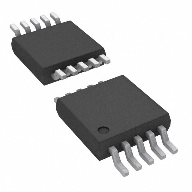
| 供应商器件封装 | 10-SOIC |
| 其它名称 | LV5980MD-AHOSCT |
| 包装 | 剪切带 (CT) |
| 同步整流器 | 无 |
| 安装类型 | 表面贴装 |
| 封装/外壳 | 10-SOP(0.154",3.90mm 宽) |
| 工作温度 | -40°C ~ 85°C |
| 标准包装 | 1 |
| 电压-输入 | 4.5 V ~ 23 V |
| 电压-输出 | 可调至 1.235V |
| 电流-输出 | 3A |
| 类型 | 降压(降压) |
| 输出数 | 1 |
| 输出类型 | 可调式 |
| 频率-开关 | 370kHz |


- 商务部:美国ITC正式对集成电路等产品启动337调查
- 曝三星4nm工艺存在良率问题 高通将骁龙8 Gen1或转产台积电
- 太阳诱电将投资9.5亿元在常州建新厂生产MLCC 预计2023年完工
- 英特尔发布欧洲新工厂建设计划 深化IDM 2.0 战略
- 台积电先进制程称霸业界 有大客户加持明年业绩稳了
- 达到5530亿美元!SIA预计今年全球半导体销售额将创下新高
- 英特尔拟将自动驾驶子公司Mobileye上市 估值或超500亿美元
- 三星加码芯片和SET,合并消费电子和移动部门,撤换高东真等 CEO
- 三星电子宣布重大人事变动 还合并消费电子和移动部门
- 海关总署:前11个月进口集成电路产品价值2.52万亿元 增长14.8%


PDF Datasheet 数据手册内容提取
Ordering number : ENA2233 LV5980MD Bi-CMOS IC L ow power consumption and highefficiency http://onsemi.com Step-down Switching Regulator Overview LV5980MD is 1ch DCDC converter with built-in power Pch MOSFET. The recommended operating range is 4.5V to 23V. The maximum current is 3A. The operating current is about 63μA, and low power consumption is achieved. Features and Functions • 1ch SBD rectification DCDC converter IC with built-in power Pch MOSFET SOIC10 • Typical value of light load mode current is 63μA • 4.5V to 23V Operating input voltage range • 100mΩ High-side switch • Output voltage adjustable to 1.235V • The oscillatory frequency is 370kHz • ON/OFF Function • built-in OCP circuit with P-by-P method • When P-by-P is generated continuously, it shifts to the HICCUP operation • External capacitor Soft-start • Under voltage lock-out, thermal shutdown Applications • Set top boxes • DVD/Blu-ray™ drivers and HDD • LCD monitors and TVs • Point of load DC/DC converters • Office Equipment • POS System • White Goods Application Circuit Example VIN Efficiency C1 C3 100 VOUT = 5V VIN=8V EN 10×μ2F 1μF PDR VIN SW D1 L1 10μRH3 C2 VO5VUT 8900 VIN=12V VIN=15V EN 70 10μF % REF LV5980MD FB ×3 -- 60 R2 cy 50 n R1 VIN CSSO/MHPICCUP Efficie 40 47kΩ 30 C4 C6 C5 SUBGND GND CC12:: GC2R1M0321JCB0BJ3110E61M0 6[TKD [mK]urata] 20 1μF 4.7nF 2.2nF L1: FDVE1040-100M [TOKO] 10 D1: SB3003CH [ON] 0 0.1 2 3 571 2 3 5710 2 3 57100 2 3 5710002 3 5710000 Load current -- mA ORDERING INFORMATION See detailed ordering and shipping information on page 20 of this data sheet. Semiconductor Components Industries, LLC, 2013 October, 2013 O3013NK 20131009-S00001 No.A2233-1/20
LV5980MD Specifications Absolute Maximum Ratings at Ta = 25°C Parameter Symbol Conditions Ratings Unit Input voltage VIN max 25 V Allowable pin voltage VIN-SW 30 V EN VIN VIN-PDR 6 V REF 6 V SS/HICCUP REF V FB REF V COMP REF V Allowable power dissipation Pd max Specified substrate *1 1.3 W Operating temperature TOPR -40 to +85 °C Storage temperature TSTG -55 to +150 °C *1 Specified substrate: 50.0 mm × 50.0 mm × 1.6 mm, fiberglass epoxy printed circuit board, 4 layers Caution 1) Absolute maximum ratings represent the values which cannot be exceeded for any length of time. Caution 2) Even when the device is used within the range of absolute maximum ratings, as a result of continuous usage under high temperature, high current, high voltage, or drastic temperature change, the reliability of the IC may be degraded. Please contact us for the further details. StressesexceedingMaximumRatingsmaydamagethedevice.MaximumRatingsarestressratingsonly.FunctionaloperationabovetheRecommendedOperating Conditions is not implied. Extended exposure to stresses above the Recommended Operating Conditions may affect device reliability. *1 Specified substrate : 50.0mm × 50.0mm × 1.6mm, fiberglass epoxy printed circuit board, 4 layers Recommended Operating Conditions at Ta = 25°C Parameter Symbol Conditions Ratings Unit Input voltage range VIN 4.5 to 23 V Electrical Characteristics at Ta=25°C, VIN=15V Characteristic Symbol Conditions Min. Typ. Max. Units [Reference Voltage] Internal Reference Voltage V 1.210 1.235 1.260 V REF V V V Pch Drive Voltage V I =0 ~ -5mA IN IN IN V PDR OUT -5.5 -5.0 -4.5 [Saw Wave Oscillator] Oscillatory Frequency F 310 370 430 kHz OSC [ON/OFF Circuit] IC startup voltage (EN PIN) VCNT_ON 2.0 VIN V Disable voltage (EN PIN) VCNT_OFF 0.3 V [Soft Start Circuit] Soft Start • Source Current I 1.2 1.8 2.4 uA SS_SC V = 3V, EN > 2V Soft Start • Sink Current I IN 300 uA SS_SK V = 0.4V SS [UVLO Circuit] UVLO Release Voltage V FB = COMP 3.3 3.7 4.1 V UVLON UVLO Lock Voltage V FB = COMP 3.02 3.42 3.82 V UVLOF [Error Amplifier] Input Bias Current I -100 -10 nA EA_IN Error amplifier gain G 100 220 380 uA/V EA Output Sink Current I FB = 1.75V -30 -17 -8 uA EA_OSK Output Source Current I FB = 0.75V 8 17 30 uA ES_OSC [Over Current Limit Circuit] Current Limit Peak I *2 Test circuit 3.5 4.7 6.2 A CL HICCUP Timer Start-up Cycle N 15 cycle CYC HICCUP Comparator Threshold V 0.15 V Voltage tHIC HICCUP Timer Discharge Current I 0.25 uA HIC Continued on next page. No.A2233-2/20
LV5980MD Continued from preceding page. Characteristic Symbol Conditions Min. Typ. Max. Units [PWM Comparator] Maximum On-Duty D 94 % MAX [Output] Output On Resistance R Io = 0.5A 100 mΩ ON [The entire device] Standby current I EN < 0.3V 1 uA CCS Light Load Mode Consumption I No switching 63 83 uA Current SLEEP Thermal Shutdown TSD *3 Design guarantee 170 °C *2 Test circuit *3 Design guarantee: Signifies target value in design. These parameters are not tested in an independent IC. Pdmax - Ta 2.0 1.5 1.3 1.0 0.68 0.5 0 0 20 40 60 80 100 No.A2233-3/20
LV5980MD Specified substrate Top Bottom 2nd/3rd layers No.A2233-4/20
LV5980MD Pin Connections Pin Function Description Pin Pin Name Description 1 SW High-side Pch MOSFET drain Pin. Pch MOSFET gate drive Voltage. 2 PDR The bypass capacitor is necessarily connected between this pin and Vin. 3 GND Ground Pin. Ground pin voltage is reference voltage Capacitor connection pin for soft start and setting re-startup cycle in HICCUP mode. 4 SS/HICCUP About 1.8uA current charges the soft start capacitor. Error Amplifier Output Pin. The phase compensation network is connected between GND pin and COMP pin. Thanks to current-mode control, comp pin voltage would tell you the output current amplitude. Comp pin is 5 COMP connected internally to an Init.comparator which compares with 0.9V reference. If comp pin voltage is larger than 0.9V, IC operates in “continuous mode”. If comp pin voltage is smaller than 0.9V, IC operates in “discontinuous mode (low consumption mode)”. Error amplifier reverse input pin. 6 FB ICs make its voltage keep 1.235V. Output voltage is divided by external resistances and it across FB. 7 REF Reference voltage. 8 SUBGND Short-circuited and use 3pin and 8pin as GND 9 EN ON/OFF Pin. Supply voltage pin. 10 VIN It is observed by the UVLO function. When its voltage becomes 3.7V or more, ICs startup in soft start. No.A2233-5/20
LV5980MD Block Diagram No.A2233-6/20
LV5980MD Pin Equivalent Circuit Pin No. Pin Name Equivalent Circuit 1 SW 2 PDR 3 GND VIN 10k 1k 10k 4 SS/HICCUP SS/HICCUP 1k GND To the next page No.A2233-7/20
LV5980MD From the previous page Pin No. Pin Name Equivalent Circuit 5 COMP 6 FB 7 REF 8 SUBGND To the next page No.A2233-8/20
LV5980MD From the previous page Pin No. Pin Name Equivalent Circuit 9 EN 10 VIN No.A2233-9/20
LV5980MD Typical Performance Characteristics Application Curves at Ta = 25°C Efficiency Efficiency 100 100 VOUT = 1.235V VOUT = 1.8V 90 90 VIN=5V 80 VIN=5V 80 15V % 70 15V % 70 8V 12V -- 60 8V 12V -- 60 y y c c cien 50 cien 50 Effi 40 Effi 40 30 30 20 20 10 10 0.1 2 3 571 2 3 5710 2 3 57100 2 3 5710002 3 5710000 0.1 2 3 571 2 3 5710 2 3 57100 2 3 5710002 3 5710000 Load current -- mA Load current -- mA Efficiency Efficiency 100 100 90 VOUT = 3.3V VIN=5V 90 VOUT = 5V VIN=8V 15V 80 15V 80 12V 12V 8V % 70 % 70 -- 60 -- 60 y y nc nc Efficie 4500 Efficie 4500 30 30 20 20 10 10 0.1 2 3 571 2 3 5710 2 3 57100 2 3 5710002 3 5710000 0.1 2 3 571 2 3 5710 2 3 57100 2 3 5710002 3 5710000 Load current -- mA Load current -- mA Operation Waveforms (Circuit from Typical Application, Ta = 25°C, VIN = 15V, VOUT = 5V) Light load mode OutputVoltage IOUT = 10mA IOUT = 10mA VSW VOUT 5V/DIV 20mV/DIV IL IL 0.5A/DIV 0.5A/DIV 10μs/DIV 10μs/DIV No.A2233-10/20
LV5980MD Discontinious current mode Output Voltage IOUT = 200mA IOUT = 200mA VSW VOUT 5V/DIV 20mV/DIV IL IL 0.5A/DIV 0.5A/DIV 2μs/DIV 2μs/DIV Continious current mode Output Voltage IOUT = 2A IOUT = 2A VSW VOUT 5V/DIV 20mV/DIV IL IL 1A/DIV 1A/DIV 2μs/DIV 2μs/DIV Load Transient response Soft start and shutdown IOUT = 0.5 (cid:81) 2.5A, Slew Rate = 100μS IOUT = 2A VIN VOUT 20V/DIV 0.2V/DIV VSS/HICCUP 2V/DIV IOUT 2A/DIV VOUT 2V/DIV 500μs/DIV 2ms/DIV Over current protection OUT - GND short VOUT 5V/DIV VSS/HICCUP 5V/DIV VSW 20V/DIV IOUT 5A/DIV 20ms/DIV No.A2233-11/20
LV5980MD Characterization Curves at Ta = 25°C, VIN = 15V Light Load Mode Consumption Current Internal Reference Voltage 90 1.26 80 V 1.25 A 70 e -- nt -- μ 5600 e voltag 1.24 Input curre 3400 nal referenc 1.23 20 nter 1.22 I 10 0 1.21 --50 --25 0 25 50 75 100 125 150 --50 --25 0 25 50 75 100 125 150 Temperature -- °C Temperature -- °C Output on resistance Current limit peak 160 5 140 4.9 Ω m 120 A 4.8 e -- 100 k -- 4.7 anc pea put on resist 6800 urrent limit 44..56 ut 40 C 4.4 O 20 4.3 0 4.2 --50 --25 0 25 50 75 100 125 150 --50 --25 0 25 50 75 100 125 150 Temperature -- °C Temperature -- °C Oscillatory Frequency UVLO 400 3.8 390 3.7 Hz 380 UVLO release voltage k equency -- 333567000 oltage -- V 33..56 y fr 340 O v cillator 330 UVL 3.4 UVLO lock voltage Os 320 3.3 310 300 3.2 --50 --25 0 25 50 75 100 125 150 --50 --25 0 25 50 75 100 125 150 Temperature -- °C Temperature -- °C Soft Start Source Current HICCUP Timer Discharge Current 2 0.33 A 0.31 μ ce current -- μA 11..89 -harge current - 000...222579 Soft start sour 11..67 UP timer Disc 00..2213 C C 0.19 HI 1.5 0.17 --50 --25 0 25 50 75 100 125 150 --50 --25 0 25 50 75 100 125 150 Temperature -- °C Temperature -- °C No.A2233-12/20
LV5980MD EN Current IC startup EN voltage 5 2.0 1.8 4 1.6 3 1.4 2 1.2 1 1.0 0 0.8 -50 -25 0 25 50 75 100 125 150 -50 -25 0 25 50 75 100 125 150 No.A2233-13/20
LV5980MD Detailed Description Power-save Feature The LV5980MC has Power-saving feature to enhance efficiency when the load is light. By shutting down unnecessary circuits, operating current of the IC is minimized and high efficiency is realized. Output Voltage Setting Output voltage (VOUT) is configurable by the resistance R3 between VOUT and FB and the R2 between FB and GND. VOUT is given by the following equation (1). R3 R3 VOUT = (1 + R2 ) × VREF = (1 + R2 ) × 1.235 [V] (1) Soft Start Soft start time (TSS) is configurable by the capacitor (C5) between SS/HICCUP and GND. The setting value of TSS is given by the equation (2). VREF 1.235 TSS = C5 × ISS = C5 × 1.8 × 10-6 [ms] (2) Hiccup Over-Current Protection Over-current limit (ICL) is set to 4.7A in the IC. When the peak value of inductor current is higher than 4.7A for 15 consecutive times, the protection deems it as over current and stops the IC. Stop period (THIC) is defined by the discharging time of the SS/HICCUP. When SS/HICCUP is lower than 0.15V, the IC starts up. When SS/HICCUP is higher than 0.3V and then over current is detected, the IC stops again. And when SS/HICCUP is higher than 1.235V, the discharge starts again. When the protection does not detect over-current status, the IC starts up again. The IC stops when the peak value of inductor current is higher than overcurrent limit for 15 consecutive times. ICL IL * The stop time defined by the discharging time of the SS/HICCUP. The IC starts up when SS/HICCUP is lower than 0.15V. SS/HICCUP THIC •The IC stops when SS/HICCUP is higher than 0.3V and overcurrent is detected. 1.235V •The IC starts up again if no overcurrent is 0.3V detected. 0.15V FB No.A2233-14/20
LV5980MD Design Procedure Inductor Selection When conditions for input voltage, output voltage and ripple current are defined, the following equations (3) give inductance value. VIN - VOUT L = × TON (3) ΔIR 1 TON = {((VIN - VOUT) ÷ (VOUT + VF)) + 1} × FOSC FOSC : Oscillatory Frequency VF : Forward voltage of Schottky Barrier diode VIN : Input voltage VOUT : Output voltage • Inductor current: Peak value (IRP) Current peak value (IRP) of the inductor is given by the equation (4). VIN - VOUT IRP = IOUT + 2L × TON (4) Make sure that rating current value of the inductor is higher than a peak value of ripple current. • Inductor current: ripple current (∆IR) Ripple current (∆IR) is given by the equation (5). VIN - VOUT ΔIR = × TON (5) L When load current (IOUT) is less than 1/2 of the ripple current, inductor current flows discontinuously. Output Capacitor Selection Make sure to use a capacitor with low impedance for switching power supply because of large ripple current flows through output capacitor. This IC is a switching regulator which adopts current mode control method. Therefore, you can use capacitor such as ceramic capacitor and OS capacitor in which equivalent series resistance (ESR) is exceedingly small. Effective value is given by the equation (6) because the ripple current (AC) that flows through output capacitor is saw tooth wave. 1 VOUT × (VIN - VOUT) IC_OUT = × [Arms] (6) 2√3 L × FOSC × VIN Input Capacitor Selection Ripple current flows through input capacitor which is higher than that of the output capacitors. Therefore, caution is also required for allowable ripple current value. The effective value of the ripple current flows through input capacitor is given by the equation (7). IC_IN = √D (1 - D) × IOUT [Arms] (7) TON VOUT D = = T VIN In (7), D signifies the ratio between ON/OFF period. When the value is 0.5, the ripple current is at a maximum. Make sure that the input capacitor does not exceed the allowable ripple current value given by (7). With (7), if VIN=15V, VOUT=5V, IOUT=1.0A and FOSC=370 kHz, then IC_IN value is about 0.471Arms. In the board wiring from input capacitor, VIN to GND, make sure that wiring is wide enough to keep impedance low because of the current fluctuation. Make sure to connect input capacitor near output capacitor to lower voltage bound due to regeneration current.When change of load current is excessive (IOUT: high ⇒ low), the power of output electric capacitor is regenerated to input capacitor. If input capacitor is small, input voltage increases. Therefore, you need to implement a large input capacitor. Regeneration power changes according to the change of output voltage, inductance of a coil and load current. No.A2233-15/20
LV5980MD Selection of external phase compensation component This IC adopts current mode control which allows use of ceramic capacitor with low ESR and solid polymer capacitor such as OS capacitor for output capacitor with simple phase compensation. Therefore, you can design long-life and high quality step-down power supply circuit easily. Frequency Characteristics The frequency characteristic of this IC is constituted with the following transfer functions. (1) Output resistance breeder : HR (2) Voltage gain of error amplifier : GVEA Current gain : GMEA (3) Impedance of phase compensation external element : ZC (4) Current sense loop gain : GCS (5) Output smoothing impedance : ZO VIN 1/GCS OSC Current sence loop FB GVER D Q GMER CLK C R SW COMP VOUT VREF CC R2 ZC HR CO RL RC R1 ZO Closed loop gain is obtained with the following formula (8). G = HR • GMER • ZC • GCS • ZO VREF 1 RL = VOUT • GMER • RC + SCC • GCS • 1 + SCO • RL (8) Frequency characteristics of the closed loop gain is given by pole fp1 consists of output capacitor CO and output load resistance RL, zero point fz consists of external capacitor CC of the phase compensation and resistance RC, and pole fp2 consists of output impedance ZER of error amplifier and external capacitor of phase compensation CC as shown in formula (8). fp1, fz, fp2 are obtained with the following equations (9) to (11). 1 fp1 = (9) 2π • CO • RL 1 fz = (10) 2π • CC • RC 1 fp2 = (11) 2π • ZER • CC No.A2233-16/20
LV5980MD Calculation of external phase compensation constant Generally, to stabilize switching regulator, the frequency where closed loop gain is 1 (zero-cross frequency fZC) should be 1/10 of the switching frequency (or 1/5). Since the switching frequency of this IC is 370kHz, the zero-cross frequency should be 37kHz. Based on the above condition, we obtain the following formula (12). VREF 1 RL VOUT • GMER • RC + SCC • GCS • 1 + SCO • RL = 1 (12) As for zero-cross frequency, since the impedance element of phase compensation is RC >>1/SCC, the following equation (13) is obtained. VREF RL • GMER • RC • GCS • = 1 (13) VOUT 1 + 2π • fZC • CO • RL Phase compensation external resistance can be obtained with the following formula (14), the variation of the formula (13). Since 2π • fZC • CO • RL >> 1 in the equation (14), we know that the external resistance is independent of load resistance. VOUT 1 1 1 + 2π • fZC • CO • RL RC = VREF • GMER • GCS • RL (14) When output is 5V and load resistance is 5Ω (1A load), the resistances of phase compensation are as follows. GCS = 2.7A/V, GMER = 220μA/V, fZC = 37kHz 5 1 1 1 + 2 × 3.14 × (37 × 103) × (30 × 10-6) × 5 RC = 1.235 × 220 × 10-6 × 2.7 × 5 = 48.898…× 103 = 48.90 [kΩ] If frequency of zero point fz and pole fp1 are in the same position, they cancel out each other. Therefore, only the pole frequency remains for frequency characteristics of the closed loop gain. In other words, gain decreases at -20dB/dec and phase only rotates by 90º and this allows characteristics where oscillation never occurs. fp1 = fz 1 1 • 2π • CO • RL 2π • CO • RC RL • CO 5 × (30 × 10-6) CC = RC • 48.9 × 103 = 3.067…× 10-9 = 3.07 [nF] The above shows external compensation constant obtained through ideal equations. In reality, we need to define phase constant through testing to verify constant IC operation at all temperature range, load range and input voltage range. In the evaluation board for delivery, phase compensation constants are defined based on the above constants. The zero-cross frequency required in the actual system board, in other word, transient response is adjusted by external compensation resistance. Also, if the influence of noise is significant, use of external phase compensation capacitor with higher value is recommended. No.A2233-17/20
LV5980MD Caution in pattern design Pattern design of the board affects the characteristics of DC-DC converter. This IC switches high current at a high speed. Therefore, if inductance element in a pattern wiring is high, it could be the cause of noise. Make sure that the pattern of the main circuit is wide and short. Orange :Hi Side MOSFET ON Red :Hi Side MOSFET OFF (1) Pattern design of the input capacitor Connect a capacitor near the IC for noise reduction between VIN and the GND. The change of current is at the largest in the pattern between an input capacitor and VIN as well as between GND and an input capacitor among all the main circuits. Hence make sure that the pattern is as fat and short as possible. (2) Pattern design of an inductor and the output capacitor High electric current flows into the choke coil and the output capacitor. Therefore this pattern should also be as fat and short as possible. (3) Pattern design with current channel into consideration Make sure that when High side MOSFET is ON (red arrow) and OFF (orange arrow), the two current channels runs through the same channel and an area is minimized. (4) Pattern design of the capacitor between VIN-PDR Make sure that the pattern of the capacitor between VIN and PDR is as short as possible. OUT (5) Pattern design of the small signal GND The GND of the small signal should be separated from the power GND. FB (6) Pattern design of the FB-OUT line Wire the line shown in red between FB and OUT to the output capacitor as near as possible. When the influence of noise is significant, use of feedback resistors R2 and R3 with lower value is recommended. Fig: FB-OUT Line No.A2233-18/20
LV5980MD PAKAGE DIMENSIONS SOIC-10NB CASE 751BQ-01 ISSUE A 2X 0.10 C A-B NOTES: 1. DIMENSIONING AND TOLERANCING PER D ASME Y14.5M, 1994. 2. CONTROLLING DIMENSION: MILLIMETERS. D 3. DIMENSION b DOES NOT INCLUDE DAMBAR A PROTRUSION. ALLOWABLE PROTRUSION 2X SHALL BE 0.10mm TOTAL IN EXCESS OF ’b’ 0.10 C A-B F AT MAXIMUM MATERIAL CONDITION. 4. DIMENSIONS D AND E DO NOT INCLUDE 10 6 MOLD FLASH, PROTRUSIONS, OR GATE BURRS. MOLD FLASH, PROTRUSIONS, OR GATE BURRS SHALL NOT EXCEED 0.15mm H E PER SIDE. DIMENSIONS D AND E ARE DE- TERMINED AT DATUM F. 1 5. DIMENSIONS A AND B ARE TO BE DETERM- 5 L2 A3 INED AT DATUM F. L C SPELAATNIENG 6. AFR1 OISM D TEHFEIN SEEDA ATISN TGH PEL VAENRET TICOA TLH DEI SLTOAWNECSET 0.20 C 10Xb DETAIL A POINT ON THE PACKAGE BODY. B 2X 5 TIPS 0.25 M C A-B D MILLIMETERS TOP VIEW DIM MIN MAX A 1.25 1.75 A1 0.10 0.25 10X h A3 0.17 0.25 0.10 C X 45 b 0.31 0.51 0.10 C D 4.80 5.00 M E 3.80 4.00 e 1.00 BSC H 5.80 6.20 A h 0.37 REF L 0.40 1.27 A1 e C SEATING DETAIL A L2 0.25 BSC SIDE VIEW PLANE END VIEW M 0 8 GENERIC RECOMMENDED MARKING DIAGRAM* SOLDERING FOOTPRINT* 10 1.00 10X0.58 PITCH XXXXX ALYWX 1 6.50 XXXXX = Specific Device Code A = Assembly Location L = Wafer Lot Y = Year W = Work Week 1 = Pb−Free Package 10X1.18 DIMENSION: MILLIMETERS *This information is generic. Please refer to device data sheet for actual part *For additional information on our Pb−Free strategy and soldering marking. Pb−Free indicator, “G”, may details, please download the ON Semiconductor Soldering and or not be present. Mounting Techniques Reference Manual, SOLDERRM/D. No.A2233-19/20
LV5980MD ORDERING INFORMATION Device Package Shipping (Qty / Packing) SOIC10 LV5980MD-AH (Pb-Free / Halogen Free) 2500 / Tape & Reel ONSemiconductorandtheONlogoareregisteredtrademarksofSemiconductorComponentsIndustries,LLC(SCILLC).SCILLCownstherightstoanumber of patents, trademarks, copyrights, trade secrets, and other intellectual property. A listing of SCILLC’s product/patent coverage may be accessed at www.onsemi.com/site/pdf/Patent-Marking.pdf.SCILLCreservestherighttomakechangeswithoutfurthernoticetoanyproductsherein.SCILLCmakesno warranty,representationorguaranteeregardingthesuitabilityofitsproductsforanyparticularpurpose,nordoesSCILLCassumeanyliabilityarisingoutofthe applicationoruseofanyproductorcircuit,andspecificallydisclaimsanyandallliability,includingwithoutlimitationspecial,consequentialorincidental damages.“Typical”parameterswhichmaybeprovidedinSCILLCdatasheetsand/orspecificationscananddovaryindifferentapplicationsandactual performancemayvaryovertime.Alloperatingparameters,including“Typicals” mustbevalidatedforeachcustomerapplicationbycustomer’stechnical experts.SCILLCdoesnotconveyanylicenseunderitspatentrightsnortherightsofothers.SCILLCproductsarenotdesigned,intended,orauthorizedforuse ascomponentsinsystemsintendedforsurgicalimplantintothebody,orotherapplicationsintendedtosupportorsustainlife,orforanyotherapplicationin whichthefailureoftheSCILLCproductcouldcreateasituationwherepersonalinjuryordeathmayoccur.ShouldBuyerpurchaseoruseSCILLCproductsfor anysuchunintendedorunauthorizedapplication,BuyershallindemnifyandholdSCILLCanditsofficers,employees,subsidiaries,affiliates,anddistributors harmlessagainstallclaims,costs,damages,andexpenses,andreasonableattorneyfeesarisingoutof,directlyorindirectly,anyclaimofpersonalinjuryor deathassociatedwithsuchunintendedorunauthorizeduse,evenifsuchclaimallegesthatSCILLCwasnegligentregardingthedesignormanufactureofthe part. SCILLC is an Equal Opportunity/Affirmative Action Employer. This literature is subject to all applicable copyright laws and is not for resale in any manner. PS No.A2233-20/20