ICGOO在线商城 > 集成电路(IC) > PMIC - 稳压器 - DC DC 开关稳压器 > TPS55010RTER

 Datasheet下载
- 型号: TPS55010RTER
- 制造商: Texas Instruments
- 库位|库存: xxxx|xxxx
- 要求:
| 数量阶梯 | 香港交货 | 国内含税 |
| +xxxx | $xxxx | ¥xxxx |
查看当月历史价格
查看今年历史价格
TPS55010RTER产品简介:
ICGOO电子元器件商城为您提供TPS55010RTER由Texas Instruments设计生产,在icgoo商城现货销售,并且可以通过原厂、代理商等渠道进行代购。 TPS55010RTER价格参考。Texas InstrumentsTPS55010RTER封装/规格:PMIC - 稳压器 - DC DC 开关稳压器, 可调式 反激 开关稳压器 IC 正或负,可提供隔离 3.3V 1 输出 16-WFQFN 裸露焊盘。您可以下载TPS55010RTER参考资料、Datasheet数据手册功能说明书,资料中有TPS55010RTER 详细功能的应用电路图电压和使用方法及教程。
TPS55010RTER 是 Texas Instruments(德州仪器)推出的一款 PMIC(电源管理集成电路),属于 DC-DC 开关稳压器类别。它具有高效能、小尺寸和高集成度的特点,适用于多种便携式电子设备和低功耗应用场景。以下是 TPS55010RTER 的主要应用场景:

 1. 便携式消费电子产品
   - 智能手机和平板电脑:TPS55010RTER 的高效转换能力和小封装设计使其非常适合为智能手机和平板电脑中的各种模块供电,例如处理器、存储器和其他外围组件。
   - 可穿戴设备:如智能手表、健身追踪器等,这些设备对电池寿命要求极高,TPS55010RTER 的低静态电流和高效率特性可以显著延长设备的续航时间。

 2. 物联网 (IoT) 设备
   - 传感器节点:在 IoT 网络中,传感器节点通常需要低功耗电源解决方案。TPS55010RTER 能够提供稳定的电压输出,同时减少能量损耗。
   - 无线通信模块:支持蓝牙、Wi-Fi 或 Zigbee 的模块可以通过 TPS55010RTER 实现高效的电源管理,确保长时间运行。

 3. 工业自动化与控制
   - 数据采集系统:在工业环境中,TPS55010RTER 可以为数据采集模块提供稳定且高效的电源,支持远程监控和控制。
   - 嵌入式控制器:用于工厂自动化或机器人系统的嵌入式控制器需要可靠的电源供应,TPS55010RTER 的高性能表现能够满足这一需求。

 4. 医疗电子设备
   - 便携式医疗仪器:如血糖仪、脉搏血氧仪等,这些设备需要精确的电源管理以保证测量结果的准确性。TPS55010RTER 的高精度输出电压特性非常适合此类应用。
   - 健康监测设备:包括心率监测器和睡眠追踪器等,TPS55010RTER 的低功耗特点有助于延长电池寿命。

 5. 其他应用场景
   - 汽车电子:可用于车载信息娱乐系统或高级驾驶辅助系统(ADAS)中的低功耗子系统。
   - 电池供电设备:如手持扫描仪、便携式打印机等,TPS55010RTER 的高效转换能力能够最大限度地利用电池电量。

综上所述,TPS55010RTER 凭借其高效率、低功耗和紧凑的设计,广泛应用于便携式设备、物联网、工业自动化以及医疗电子等领域,为现代电子设备提供了可靠的电源解决方案。
| 参数 | 数值 |
| 产品目录 | 集成电路 (IC)半导体 |
| 描述 | IC REG MULTI CONFIG SYNC 16WQFN稳压器—开关式稳压器 2.95-6Vin,2W,Iso DC/DC Converter |
| 产品分类 | |
| 品牌 | Texas Instruments |
| 产品手册 | |
| 产品图片 |
|
| rohs | 符合RoHS无铅 / 符合限制有害物质指令(RoHS)规范要求 |
| 产品系列 | 电源管理 IC,稳压器—开关式稳压器,Texas Instruments TPS55010RTER- |
| 数据手册 | |
| 产品型号 | TPS55010RTER |
| PCN组件/产地 | |
| PWM类型 | 电流模式 |
| 产品种类 | 稳压器—开关式稳压器 |
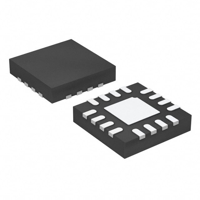
| 供应商器件封装 | 16-WQFN(3x3) |
| 其它名称 | 296-28950-6 |
| 包装 | Digi-Reel® |
| 参考设计库 | http://www.digikey.com/rdl/4294959904/4294959903/435 |
| 同步整流器 | 是 |
| 商标 | Texas Instruments |
| 安装类型 | 表面贴装 |
| 安装风格 | SMD/SMT |
| 封装 | Reel |
| 封装/外壳 | 16-WFQFN 裸露焊盘 |
| 封装/箱体 | WQFN-16 |
| 工作温度 | -40°C ~ 150°C |
| 工作温度范围 | - 40 C to + 150 C |
| 工厂包装数量 | 3000 |
| 开关频率 | 500 kHz |
| 拓扑结构 | Buck, Flyback |
| 最大工作温度 | + 150 C |
| 最大输入电压 | 6 V |
| 最小工作温度 | - 40 C |
| 最小输入电压 | 2.95 V |
| 标准包装 | 1 |
| 电压-输入 | 2.95 V ~ 6 V |
| 电压-输出 | 3.3 V ~ 20 V |
| 电流-输出 | 100mA |
| 类型 | 降压(降压),回扫,隔离式 |
| 系列 | TPS55010 |
| 输入电压 | 2.95 V to 6 V |
| 输出数 | 1 |
| 输出电压 | 3.3 V to 20 V |
| 输出电流 | 400 mA |
| 输出端数量 | 2 Output |
| 输出类型 | 可调式 |
| 配用 | /product-detail/zh/TPS55010EVM-009/296-28812-ND/2667043/product-detail/zh/TPS55010EVM-051/296-31208-ND/2768992 |
| 频率-开关 | 100kHz ~ 2MHz |


- 商务部:美国ITC正式对集成电路等产品启动337调查
- 曝三星4nm工艺存在良率问题 高通将骁龙8 Gen1或转产台积电
- 太阳诱电将投资9.5亿元在常州建新厂生产MLCC 预计2023年完工
- 英特尔发布欧洲新工厂建设计划 深化IDM 2.0 战略
- 台积电先进制程称霸业界 有大客户加持明年业绩稳了
- 达到5530亿美元!SIA预计今年全球半导体销售额将创下新高
- 英特尔拟将自动驾驶子公司Mobileye上市 估值或超500亿美元
- 三星加码芯片和SET,合并消费电子和移动部门,撤换高东真等 CEO
- 三星电子宣布重大人事变动 还合并消费电子和移动部门
- 海关总署:前11个月进口集成电路产品价值2.52万亿元 增长14.8%


PDF Datasheet 数据手册内容提取
Product Sample & Technical Tools & Support & Folder Buy Documents Software Community TPS55010 SLVSAV0B–APRIL2011–REVISEDOCTOBER2014 TPS55010 2.95-V To 6-V Input, 2 W, Isolated DC/DC Converter with Integrated FETs 1 Features 3 Description • IsolatedFly-Buck™Topology The TPS55010 is a transformer driver designed to 1 provideisolatedpowerforisolatedinterfaces,suchas • PrimarySideFeedback RS-485andRS-232,from3.3Vor5Vinputsupply. • 100kHzto2000kHzSwitchingFrequency Thedeviceusesfixedfrequencycurrentmodecontrol • SynchronizestoExternalClock and half bridge power stage with primary side • AdjustableSlowStart feedback to regulate the output voltage for power • AdjustableInputVoltageUVLO levels up to 2W. The switching frequency is adjustablefrom100kHzto2000kHzsosolutionsize, • OpenDrainFaultOutput efficiency and noise can be optimized. The switching • Cycle-by-CycleCurrentLimit frequency is set with a resistor or is synchronized to • ThermalShutdownProtection external clock using the RT/CLK pin. To minimize inrush currents, a small capacitor can be connected • 3mmx3mm16PinQFNPackage to the SS pin. The EN pin can be used as an enable pin or to increase the default input UVLO voltage 2 Applications from2.6V. • NoiseImmunityinPLCs,DataAcquisitionand With the same transformer the TPS55010 can MeasurementEquipment provide a solution for different input and output • IsolatedRS-232andRS-485Communication voltage combinations by adjusting the primary side Channels voltage. Off the shelf transformers are available to • PowersLineDrivers,ISOAmplifiers,Sensors, provide single positive, or dual positive and negative outputvoltages. CANTransceivers • FloatingSuppliesforIGBTGateDrivers The TPS55010 is available in a 3mm x 3mm 16 pin QFNpackagewiththermalpad. • PromotesSafetyinMedicalEquipment DeviceInformation (1) PARTNUMBER PACKAGE BODYSIZE(NOM) TPS55010 WQFN(16) 3.00mm×3.00mm (1) Forallavailablepackages,seetheorderableaddendumathe endofthedatasheet. 4 Simplified Schematic EfficiencyvsLoadCurrent 3V 100 to 90 5.5V VIN BOOT T1 5V 80 200mA C TPS55010 C 1:2.5 70 IN boot %) PH C + y ( 60 EFANULT RHS O V_O Efficienc 4500 SS VSENSE 30 VOUT = 5V RT/CLK C 20 FSW = 350kHz C COMP PRI ss Rt RC RLS 10 VIN = 5V GND 0 0.00 0.05 0.10 0.15 0.20 0.25 0.30 C C Output Current (A) G040 1 An IMPORTANT NOTICE at the end of this data sheet addresses availability, warranty, changes, use in safety-critical applications, intellectualpropertymattersandotherimportantdisclaimers.PRODUCTIONDATA.
TPS55010 SLVSAV0B–APRIL2011–REVISEDOCTOBER2014 www.ti.com Table of Contents 1 Features.................................................................. 1 8.2 FunctionalBlockDiagram.......................................10 2 Applications........................................................... 1 8.3 FeatureDescription.................................................11 3 Description............................................................. 1 8.4 DeviceFunctionalModes........................................14 4 SimplifiedSchematic............................................. 1 9 ApplicationAndImplementation........................ 17 9.1 ApplicationInformation............................................17 5 RevisionHistory..................................................... 2 9.2 TypicalApplications................................................17 6 PinConfigurationandFunctions......................... 3 9.3 TypicalApplication,DualOutput.............................29 7 Specifications......................................................... 4 10 PowerSupplyRecommendations..................... 37 7.1 AbsoluteMaximumRatings .....................................4 11 Layout................................................................... 37 7.2 HandlingRating.........................................................4 11.1 LayoutGuidelines.................................................37 7.3 RecommendedOperatingConditions.......................4 11.2 LayoutExample....................................................37 7.4 ThermalInformation..................................................5 12 DeviceandDocumentationSupport................. 38 7.5 ElectricalCharacteristics...........................................5 7.6 TimingRequirements................................................6 12.1 DeviceSupport......................................................38 7.7 SwitchingCharacteristics..........................................6 12.2 Trademarks...........................................................38 7.8 TypicalCharacteristics..............................................7 12.3 ElectrostaticDischargeCaution............................38 12.4 Glossary................................................................38 8 DetailedDescription............................................ 10 13 Mechanical,Packaging,andOrderable 8.1 Overview.................................................................10 Information........................................................... 38 5 Revision History NOTE:Pagenumbersforpreviousrevisionsmaydifferfrompagenumbersinthecurrentversion. ChangesfromRevisionA(June2011)toRevisionB Page • ChangedAddedtheDeviceinformationtable,HandlingRatingstable,ApplicationsandImplementationsection, Layoutsection,andtheDeviceandDocumentationSupportsection.................................................................................... 1 • AddedtheHandlingRatingtable............................................................................................................................................ 4 • AddedtheRecommendedOperatingConditionstable.......................................................................................................... 4 • AddedFigure23................................................................................................................................................................... 23 • AddedFigure24 .................................................................................................................................................................. 24 • ChangedFigure26throughFigure28 ................................................................................................................................ 26 • ChangedFigure40 .............................................................................................................................................................. 27 • ChangedFigure42throughFigure44 ................................................................................................................................ 34 • ChangedFigure54 .............................................................................................................................................................. 35 ChangesfromOriginal(April2010)toRevisionA Page • ChangedthedevicestatusFrom:ProductPreviewTo:Production....................................................................................... 1 2 SubmitDocumentationFeedback Copyright©2011–2014,TexasInstrumentsIncorporated ProductFolderLinks:TPS55010
TPS55010 www.ti.com SLVSAV0B–APRIL2011–REVISEDOCTOBER2014 6 Pin Configuration and Functions RTEPACKAGE (TOPVIEW) N ULT OT VI EN FA BO 16 15 14 13 VIN 1 12 PH VIN 2 Thermal 11 PH Pad GND 3 (17) 10 PH GND 4 9 SS 5 6 7 8 D E P K N S M L G N O C E C T/ S R V PinFunctions Name Number Description VIN 1,2,16 Suppliesthecontrolcircuitryandswitchesofthepowerconverter. GND 3,4,5 PowerGround.ThispinshouldbeelectricallyconnecteddirectlytothethermalpadundertheIC. VSENSE 6 Invertingnodeofthetransconductanceerroramplifier. Erroramplifieroutput,andinputtotheoutputswitchcurrentcomparator.Connectfrequency COMP 7 compensationcomponentstothispin. ResistorTimingandExternalClock.Aninternalamplifierholdsthispinatafixedvoltagewhen usinganexternalresistortogroundtosettheswitchingfrequency.Ifthepinispulledabovethe PLLupperthreshold,amodechangeoccursandthepinbecomesasynchronizationinput.The RT/CLK 8 internalamplifierisdisabledandthepinisahighimpedanceclockinputtotheinternalPLL.If clockingedgesstop,theinternalamplifierisre-enabledandthemodereturnstoaresistorset function. SS 9 Slow-start.Anexternalcapacitorconnectedtothispinsetstheoutputrisetime. PH 10,11,12 ThesourceoftheinternalhighsidepowerMOSFET,anddrainoftheinternallowsideMOSFET. AbootstrapcapacitorisrequiredbetweenBOOTandPH.Ifthevoltageonthiscapacitorisbelow BOOT 13 theminimumrequiredbytheoutputdevice,theoutputisforcedtoswitchoffuntilthecapacitoris refreshed. Anopendrainoutput.Activelowiftheoutputvoltageislowduetothermalshutdown,dropout, FAULT 14 overvoltageorENshutdown. Enablepin,internalpull-upcurrentsource.Pullbelow1.2Vtodisable.Floattoenable.Adjustthe EN 15 inputundervoltagelockoutwithtworesistors. GNDpinshouldbeconnectedtotheexposedthermalpadforproperoperation.Thisthermalpad THERMALPAD 17 shouldbeconnectedtoanyinternalPCBgroundplaneusingmultipleviasforgoodthermal performance. Copyright©2011–2014,TexasInstrumentsIncorporated SubmitDocumentationFeedback 3 ProductFolderLinks:TPS55010
TPS55010 SLVSAV0B–APRIL2011–REVISEDOCTOBER2014 www.ti.com 7 Specifications 7.1 Absolute Maximum Ratings (1) overoperatingfree-airtemperaturerange(unlessotherwisenoted) MIN MAX UNIT VIN –0.3 7 V EN –0.3 3.6 V BOOT PH+7 V VSENSE –0.3 3 V COMP –0.3 3 V Voltage FAULT –0.3 7 V SS –0.3 3 V RT/CLK –0.3 6 V BOOT-PH –0.3 7 V PH –0.6 7 V PH,10nsTransient –2 10 V EN 100 µA RT/CLK 100 µA Current COMP 100 uA FAULT 10 mA SS 100 µA OperatingJunctionTemperature –40 150 °C (1) Stressesbeyondthoselistedunderabsolutemaximumratingsmaycausepermanentdamagetothedevice.Thesearestressratings only,andfunctionaloperationofthedeviceattheseoranyotherconditionsbeyondthoseindicatedunderELECTRICAL SPECIFICATIONSisnotimplied.Exposuretoabsolute-maximum-ratedconditionsforextendedperiodsmayaffectdevicereliability. 7.2 Handling Rating overoperatingfree-airtemperaturerange(unlessotherwisenoted) MIN MAX UNIT T StorageTemperature –65 150 °C stg Humanbodymodel(HBM),perANSI/ESDA/JEDEC JS-001,allpins (1) –2 2 kV V ElectrostaticDischarge (ESD) Chargeddevicemodel(CDM),perJEDECspecification JESD22-C101,allpins (2) –500 500 V (1) JEDECdocumentJEP155statesthat500-VHBMallowssafemanufacturingwithastandardESDcontrolprocess. (2) JEDECdocumentJEP157statesthat250-VCDMallowssafemanufacturingwithastandardESDcontrolprocess. 7.3 Recommended Operating Conditions overoperatingfree-airtemperaturerange(unlessotherwisenoted) MIN NOM MAX UNIT V Inputvoltage 2.98 6 V I P Outputpower 2 W O 4 SubmitDocumentationFeedback Copyright©2011–2014,TexasInstrumentsIncorporated ProductFolderLinks:TPS55010
TPS55010 www.ti.com SLVSAV0B–APRIL2011–REVISEDOCTOBER2014 7.4 Thermal Information TPS55010 THERMALMETRIC(1) UNIT RTE(16PINS) θ Junction-to-ambientthermalresistance 60 JA θ Junction-to-case(top)thermalresistance 55.5 JCtop θ Junction-to-boardthermalresistance 24.9 JB °C/W ψ Junction-to-topcharacterizationparameter 1.0 JT ψ Junction-to-boardcharacterizationparameter 24.9 JB θ Junction-to-case(bottom)thermalresistance 9.9 JCbot (1) Formoreinformationabouttraditionalandnewthermalmetrics,seetheICPackageThermalMetricsapplicationreport,SPRA953. 7.5 Electrical Characteristics T =–40°CTO150°C,VIN=2.95VTO6V(unlessotherwisenoted) J DESCRIPTION CONDITIONS MIN TYP MAX UNIT SUPPLYVOLTAGE Operatinginputvoltage VIN 2.95 6 V Shutdowncurrent EN=0V,25°C 2 5 µA Operatingcurrent VSENSE=0.9V,25°C 360 575 µA Internalundervoltagelockout 2.6 2.9 V ENABLE rising 1.25 1.37 V Enablethreshold falling 1.15 1.18 Threshold-50mV –1.2 µA Inputcurrent Threshold+50mV –4.6 µA Hysteresis 3.4 VOLTAGEREFERENCE Reference 3V<VIN<6V 0.804 0.829 0.854 V MOSFET Highsideswitchresistance BOOT-PH=5V 45 81 mΩ Lowsideswitchresistance VIN=5V 45 81 mΩ ERRORAMPLIFIER Inputcurrent 50 nA Erroramptransconductance -2µA<I <2µA 245 uS (COMP) Errorampdcgain VSENSE=0.8V 500 V/V MinimumunitygainBandwidth 3 MHz Errorampsource/sink V =1V,100mVoverdrive ±16 µA (COMP) COMPtoIphgm I =0.5A 7.5 A/V (PH) CURRENTLIMIT Highsidesourcingcurrentlimit VIN=3V 2 2.75 A LowSideSinkingCurrentLimit VIN=3V –3 –4.5 A THERMALSHUTDOWN ThermalShutdown 171 °C OTHysteresis 12 °C Copyright©2011–2014,TexasInstrumentsIncorporated SubmitDocumentationFeedback 5 ProductFolderLinks:TPS55010
TPS55010 SLVSAV0B–APRIL2011–REVISEDOCTOBER2014 www.ti.com Electrical Characteristics (continued) T =–40°CTO150°C,VIN=2.95VTO6V(unlessotherwisenoted) J DESCRIPTION CONDITIONS MIN TYP MAX UNIT RT/CLK RT/CLKvoltage R =195kΩ 0.5 V (RT/CLK) RT/CLKhighthreshold 1.6 2.2 V RT/CLKlowthreshold 0.4 0.6 V BOOT BootUVLO 2.5 V SSSlowStart Chargecurrent V =0.4V 0.5 2.2 4 µA (SS) SStoVSENSEmatching V =0.4V 35 mV (SS) SStoreferenceCrossover 98%reference 1.1 V SSdischargecurrent(overload) VSENSE=0V 325 µA SSdischargevoltage VSENSE=0V 46 mV SSdischargecurrent(UVLO,EN,thermalfault) V =0.5V 1.2 mA (SS) VINUVLOtoSSstarttime 100 µs FAULTPin VSENSEfalling 91 %VREF VSENSEthreshold VSENSErising 108 %VREF Outputhighleakage VSENSE=V ,V =5.5V 2 nA REF (FAULT) Outputlow I =3mA 0.3 V (FAULT) MinimumVINforvalidoutput V <0.5Vat100µA 1.6 V (FAULT) 7.6 Timing Requirements MIN TYP MAX UNIT RT/CLK MinimumCLKpulsewidth 75 ns 7.7 Switching Characteristics overoperatingfree-airtemperaturerange(unlessotherwisenoted) PARAMETER TESTCONDITIONS MIN TYP MAX UNIT PH t Minimumontime Measuredat10%to10%ofVIN 130 ns on t Minimumofftime V ≥3V 0% off (BOOT-PH) RT/CLK SwitchingfrequencyusingCLKmode 300 2000 kHz SwitchingfrequencyusingRTmode 100 2000 kHz SwitchingFrequency R =195kΩ 400 500 600 kHz (RT/CLK) PLLlockintime 50 µs RT/CLKfallingedgetoPHrisingedge 90 ns delay SSSlowStart VINUVLOtoSSstarttime 100 µs 6 SubmitDocumentationFeedback Copyright©2011–2014,TexasInstrumentsIncorporated ProductFolderLinks:TPS55010
TPS55010 www.ti.com SLVSAV0B–APRIL2011–REVISEDOCTOBER2014 7.8 Typical Characteristics 90 500 VIN = 5V 80 RT = 200kW ) 70 kHz) 475 Wm 60 y ( On Resistance ( 23450000 HLoigwh SSiiddee VVININ == 55VV Oscillator Frequenc 442550 10 High Side VIN = 3.3V Low Side VIN = 3.3V 0 400 −50 −25 0 25 50 75 100 125 150 −50 −25 0 25 50 75 100 125 150 Junction Temperature (°C) Junction Temperature (°C) G001 G002 Figure1.HighSideandLowSideR Figure2.FrequencyvsTemperature DS(on) vsTemperature 3.5 −4.0 3.4 VIN = 5V −4.2 VIN = 3.3V VIN = 3.3V VIN = 5V A) 3.3 A) −4.4 old ( 3.2 old ( −4.6 h h es 3.1 es −4.8 hr hr T 3.0 T −5.0 mit mit Li 2.9 Li −5.2 ent 2.8 ent −5.4 Curr 2.7 Curr −5.6 2.6 −5.8 2.5 −6.0 −50 −25 0 25 50 75 100 125 150 −50 −25 0 25 50 75 100 125 150 Junction Temperature (°C) Junction Temperature (°C) G003 G004 Figure3.HighSideCurrentLimit(Sourcing)vs Figure4.LowSideCurrentLimit(Sinking)vs JunctionTemperature JunctionTemperature 300 1.240 VIN = 5V 1.235 250 1.230 ce (µA) 200 e (V) 11..222205 uctan 150 Enabl 1.215 RFaislliinngg anscond 100 VENA− 111...222001050 Tr 50 1.195 1.190 VIN = 5V 0 1.185 −50 −25 0 25 50 75 100 125 150 −50 −25 0 25 50 75 100 125 150 Junction Temperature (°C) Junction Temperature (°C) G005 G006 Figure5.ErrorAmplifierTransconductancevsTemperature Figure6.ENPinVoltagevsTemperature Copyright©2011–2014,TexasInstrumentsIncorporated SubmitDocumentationFeedback 7 ProductFolderLinks:TPS55010
TPS55010 SLVSAV0B–APRIL2011–REVISEDOCTOBER2014 www.ti.com Typical Characteristics (continued) −0.1 −3.24 VIN = 5V VIN = 5V −0.2 −3.26 µA) −0.3 A) −3.28 e Current ( −−00..54 ble Hyst (µ −−33..3320 bl −0.6 a a n n E −3.34 − E −0.7 A− A N −3.36 N −0.8 E E −0.9 −3.38 −1.0 −3.40 −50 −25 0 25 50 75 100 125 150 −50 −25 0 25 50 75 100 125 150 Junction Temperature (°C) Junction Temperature (°C) G007 G008 Figure7.ENPinPullup Figure8.ENPinHysteresisCurrent vsTemperature(V =Threshold-50mV) vsTemperature EN −2.0 2.76 −2.1 VIN = 5V 2.74 Rising Falling −2.2 2.72 2.70 nt (µA) −−22..43 age (V) 22..6668 VIN = 5V urre −2.5 Volt 2.64 S C −2.6 put 2.62 S −2.7 In 2.60 −2.8 2.58 −2.9 2.56 −3.0 2.54 −50 −25 0 25 50 75 100 125 150 −50 −25 0 25 50 75 100 125 150 Junction Temperature (°C) Junction Temperature (°C) G009 G010 Figure9.SSChargeCurrentvsTemperature Figure10.InputStartandStopVoltagevsTemperature 2.5 400 EN = 0V EN = Open VSENSE = 0.9V 2.0 380 µA) A) Current ( 1.5 urrent (µ 360 wn 1.0 y C 340 hutdo Suppl S 0.5 320 VIN = 5V VIN = 5V VIN = 3.3V VIN = 3.3V 0.0 300 −50 −25 0 25 50 75 100 125 150 −50 −25 0 25 50 75 100 125 150 Junction Temperature (°C) Junction Temperature (°C) G011 G012 Figure11.ShutdownSupplyCurrentvsTemperature Figure12.VINSupplyCurrentvsTemperature 8 SubmitDocumentationFeedback Copyright©2011–2014,TexasInstrumentsIncorporated ProductFolderLinks:TPS55010
TPS55010 www.ti.com SLVSAV0B–APRIL2011–REVISEDOCTOBER2014 Typical Characteristics (continued) 0.834 110 0.833 VIN = 5V 105 0.832 F) e (V) 0.831 VRE 100 nc 0.830 % Refere 0.829 shold ( 95 VIN = 5V Voltage 000...888222678 Fault Thre 8950 VSENSE Rising 0.825 VSENSE Falling 0.824 80 −50 −25 0 25 50 75 100 125 150 −50 −25 0 25 50 75 100 125 150 Junction Temperature (°C) Junction Temperature (°C) G013 G014 Figure13.VoltageReferencevsTemperature Figure14.FaultThresholdvsTemperature 160 36 VIN = 5V VIN = 5V 140 V) 35 120 m Wstance () 18000 SE Offset ( 3334 si N e E R 60 S n V 32 O 40 S to S 31 20 0 30 −50 −25 0 25 50 75 100 125 150 −50 −25 0 25 50 75 100 125 150 Junction Temperature (°C) Junction Temperature (°C) G015 G016 Figure15.FaultOn-ResistancevsTemperature Figure16.SStoVSENSEOffsetvsTemperature Copyright©2011–2014,TexasInstrumentsIncorporated SubmitDocumentationFeedback 9 ProductFolderLinks:TPS55010
TPS55010 SLVSAV0B–APRIL2011–REVISEDOCTOBER2014 www.ti.com 8 Detailed Description 8.1 Overview The TPS55010 is a half bridge transformer driver designed to implement a high efficiency, low power isolated supply. The primary side feedback implemented using two resistors and a primary side capacitor provides excellentregulationoverlineandloadcomparedtoanopenlooppushpullconverter. The half bridge power stage consists of two integrated n-channel MOSFETs with 45 mΩ on resistance. The drive voltage for the integrated high side MOSFET is supplied by a capacitor between the BOOT and PH pins. The switching frequency is adjusted using a resistor to ground on the RT/CLK pin. The device has an internal phase lock loop (PLL) on the RT/CLK pin that is used to synchronize the high side power switch turn on to a falling edge of an external system clock. The wide switching frequency of 100 kHz to 2000 kHz (300kHz to 2000kHz in CLK mode) allows for efficiency, size optimization or noise avoidance when selecting the switching frequency. The TPS55010 has a typical default start up voltage of 2.6 V. The EN pin has an internal pull-up current source that can be used to adjust the input voltage under voltage lockout (UVLO) with two external resistors. In addition, the pull up current provides a default condition when the EN pin is floating for the device to operate. The total operating current for the TPS55010 is typically 360 µA when not switching and under no load. When the device is disabled, the supply current is less than 5 µA. The slow start (SS) pin is used to minimize inrush currents duringstartup. 8.2 Functional Block Diagram FAULT EN VIN Shutdown Thermal Shutdown UVLO Enable 91% Logic Comparator Shutdown Shutdown Logic 108% Enable Threshold Boot Voltage Charge Reference Minimum Boot Clamp UVLO Current Pulse Sense ERROR Skip VSENSE AMPLIFIER PWM BOOT Comparator PWM Latch R Q SS Logic S Shutdown Logic S Slope Compensation PH COMP Current Limit Overload Maximum Recovery Clamp Oscillator GND with PLL THERMAL RT/CLK PAD 10 SubmitDocumentationFeedback Copyright©2011–2014,TexasInstrumentsIncorporated ProductFolderLinks:TPS55010
TPS55010 www.ti.com SLVSAV0B–APRIL2011–REVISEDOCTOBER2014 8.3 Feature Description 8.3.1 FixedFrequencyPWMControl The TPS55010 uses an adjustable fixed frequency, peak current mode control. The primary voltage is compared through external resistors on the VSENSE pin to an internal voltage reference by an error amplifier which drives the COMP pin. An internal oscillator initiates the turn on of the high side power switch. The error amplifier output is compared to the high side power switch current. When the power switch current reaches the COMP voltage level the high side power switch is turned off and the low side power switch is turned on. The COMP pin voltage increases and decreases as the output current increases and decreases. The device implements a current limit by clamping the COMP pin voltage to a maximum level. The TPS55010 adds a compensating ramp to the switch currentsignal.Thisslopecompensationpreventssub-harmonicoscillationsasdutycycleincreases. 8.3.2 HalfBridgeandBootstrapVoltage The TPS55010 has an integrated boot regulator and requires a small ceramic capacitor between the BOOT and PHpintoprovidethegatedrivevoltageforthehighsideMOSFET.Thevalueoftheceramiccapacitorshouldbe 0.1 µF. A ceramic capacitor with an X7R or X5R grade dielectric and a voltage rating of 10 V or higher is recommendedbecauseofthestablecharacteristicsovertemperatureandvoltage. 8.3.3 ErrorAmplifier The TPS55010 uses a transconductance error amplifier. The amplifier compares the VSENSE voltage to the lower of the SS pin voltage or the internal 0.829 V voltage reference. The transconductance of the error amplifier is245µA/V.ThefrequencycompensationcomponentsareplacedbetweentheCOMPpinandground. 8.3.4 VoltageReference The voltage reference system produces a precise ±3.0% voltage reference over temperature by scaling the output of a temperature-stable band gap circuit. The band gap and scaling circuits produce 0.829 V at the non- invertinginputoftheerroramplifier. 8.3.5 AdjustingtheOutputVoltage The primary side voltage is set with a resistor divider from the primary side capacitor to the VSENSE pin. It is recommended to use 1% tolerance or better divider resistors. Start with a 10 kΩ for the R resistor and use LS Equation 1 to calculate R . The output voltage is a function of the primary voltage, transformer turns ratio and HS forwardvoltageofthediode. æV - 0.829Vö RHS = RLS × ççççè PR0I.829V ÷÷÷÷ø (1) spacer N V = V × SEC - V OUT PRI N fd PRI (2) spacer Copyright©2011–2014,TexasInstrumentsIncorporated SubmitDocumentationFeedback 11 ProductFolderLinks:TPS55010
TPS55010 SLVSAV0B–APRIL2011–REVISEDOCTOBER2014 www.ti.com Feature Description (continued) Npri:Nsec VFD VIN PH V O TPS55010 C O VSENSE - R HS V PRI + 0.829V R LS GND C PRI Figure17. SettingtheOutputVoltage 8.3.6 EnableandAdjustingUndervoltageLockout The TPS55010 is disabled when the VIN pin voltage falls below 2.6 V. If an application requires a higher undervoltage lockout (UVLO), use the EN pin as shown in Figure 18 to adjust the input voltage UVLO by using two external resistors. The EN pin has an internal pull-up current source of 1.2 µA that provides the default condition of the TPS55010 operating when the EN pin floats. Once the EN pin voltage exceeds 1.25 V, an additional 3.4 µA of hysteresis is added. When the EN pin is pulled below 1.18 V, the hysteresis current is removed. TPS55010 VIN I I 1 hys R UVLO1 EN R UVLO2 V ENA Figure18. AdjustableUnderVoltageLockOut æ ö çV ÷ VSTARTççççVENfalling÷÷÷÷÷ - VSTOP ççè ENrising ÷ø R = UVLO1 æ V ö I1 × çççççè1- VEENNfraislliinngg÷÷÷÷÷÷ø + IHYS (3) spacer R × V UVLO1 ENfalling R = UVLO2 V - V + R × (I1 + I ) STOP ENfalling UVLO1 HYS (4) 12 SubmitDocumentationFeedback Copyright©2011–2014,TexasInstrumentsIncorporated ProductFolderLinks:TPS55010
TPS55010 www.ti.com SLVSAV0B–APRIL2011–REVISEDOCTOBER2014 Feature Description (continued) 8.3.7 AdjustingSlowStartTime A capacitor on the SS pin to ground implements a slow start time to minimize inrush current during startup. The TPS55010regulatestotheloweroftheSSpinandtheinternalreferencevoltage.TheTPS55010hasaninternal pull-up current source of 2.2 µA which charges the external slow start capacitor. Equation 5 calculates the required slow start capacitor value where T is the desired slow start time in ms, Iss is the internal slow start SS chargingcurrentof2.2 µA,andV istheinternalvoltagereferenceof0.829V. REF If during normal operation, the VIN goes below the UVLO, EN pin pulled below 1.18 V, or a thermal shutdown event occurs, the TPS55010 stops switching. When the VIN goes above UVLO, EN is released or pulled high, or a thermal shutdown is exited, then SS is discharged to below 40 mV before reinitiating a powering up sequence. The VSENSE voltage will follow the SS pin voltage with a 35 mV offset up to 85% of the internal voltage reference. When the SS voltage is greater than 85% on the internal reference voltage the offset increases as the effective system reference transitions from the SS voltage to the internal voltage reference. If no slow start time isneeded,theSSpincanbeleftopen.Theslowstartcapacitorshouldbelessthan0.47 µF. T (ms) × I (uA) SS SS C (nF) = SS V (V) REF (5) 8.3.8 ConstantSwitchingFrequencyandTimingResistor(RT/CLKPin) The switching frequency of the TPS55010 is adjustable over a wide range from 100 kHz to 2000 kHz by placing amaximumof1070kΩ andminimumof42.2kΩ,respectively,ontheRT/CLKpin.Aninternalamplifierholdsthis pin at a fixed voltage when using an external resistor to ground to set the switching frequency. The RT/CLK is typically0.5V.Todeterminethetimingresistanceforagivenswitchingfrequency,useEquation6. To reduce the solution size one would typically set the switching frequency as high as possible, but tradeoffs of the efficiency, maximum input voltage and minimum controllable on time should be considered. The minimum controllableontimeistypically130ns. 156000 R (kW)= T f (kHz)1.0793 sw (6) 8.3.9 HowtoInterfacetoRT/CLKPin The RT/CLK pin can be used to synchronize the regulator to an external system clock. To implement the synchronization feature connect a square wave to the RT/CLK pin through one of the circuit networks shown in Figure 19. The square wave amplitude must transition lower than 0.4V and higher than 2.2V on the RT/CLK pin and have a high time greater than 75 ns. The synchronization frequency range is 300 kHz to 2000 kHz. The risingedgeofthePHissynchronizedtothefallingedgeofRT/CLKpinsignal. The external synchronization circuit should be designed in such a way that the device has the default frequency set resistor connected from the RT/CLK pin to ground should the synchronization signal turn off. It is recommended to use a frequency set resistor connected as shown in Figure 19 through another resistor (e.g 50 Ω) to ground for clock signal that are not Hi-Z or tri-state during the off state. The RT resistor value should set theswitchingfrequencyclosetotheexternalCLKfrequency.Itisrecommendedtoaccouplethesynchronization signal through a 10 pF ceramic capacitor to RT/CLK pin. The first time the CLK is pulled above the CLK threshold the device switches from the RT resistor frequency to PLL mode. The internal 0.5 V voltage source is removed and the CLK pin becomes high impedance as the PLL starts to lock onto the external signal. Since there is a PLL on the regulator the switching frequency can be higher or lower than the frequency set with the external resistor. The device transitions from the resistor mode to the PLL mode and then will increase or decrease the switching frequency until the PLL locks onto the external CLK frequency within 50 microseconds. When the device transitions from the PLL to resistor mode the switching frequency will slow down from the CLK frequencyto150kHz,thenreapplythe0.5Vvoltageandtheresistorwillthensettheswitchingfrequency. Copyright©2011–2014,TexasInstrumentsIncorporated SubmitDocumentationFeedback 13 ProductFolderLinks:TPS55010
TPS55010 SLVSAV0B–APRIL2011–REVISEDOCTOBER2014 www.ti.com Feature Description (continued) TPS55010 TPS55010 RT/CLK RT/CLK PLL PLL RT Hi-Z Clock Clock RT Source Source Figure19. SynchronizingtoaSystemClock 8.3.10 OvercurrentProtection The TPS55010 implements a cycle by cycle current limit. During each switching cycle the high side switch current is compared to the voltage on the COMP pin. When the instantaneous switch current intersects the COMP voltage, the high side switch is turned off. During overcurrent conditions that pull the output voltage low, the error amplifier responds by driving the COMP pin high, increasing the switch current. The error amplifier outputisclampedinternally.Thisclampfunctionsasaswitchcurrentlimit. 8.3.11 ReverseOvercurrentProtection The TPS55010 implements low side current protection by detecting the voltage across the low side MOSFET. When the converter sinks current through its low side FET, the control circuit turns off the low side MOSFET if thereversecurrentismorethan4.5A 8.3.12 FAULTPin The FAULT pin output is an open drain MOSFET. The output is pulled low when the VSENSE voltage is below 91% or rising above 108% of the nominal internal reference voltage. It is recommended to use a pull-up resistor between the values of 1kΩ and 100kΩ to a voltage source that is 6 V or less. The FAULT pin is in a valid state once the VIN input voltage is greater than 1.6 V. The FAULT pin is pulled low, if the input UVLO or thermal shutdownisasserted,ortheENpinispulledlow. 8.3.13 ThermalShutdown The device implements an internal thermal shutdown to protect itself if the junction temperature exceeds 171°C. The thermal shutdown forces the device to stop switching when the junction temperature exceeds the thermal trip threshold. Once the die temperature decreases below 159°C, the device reinitiates the power up sequence bydischargingtheSSpintobelow40mV.Thethermalshutdownhysteresisis12°C. 8.4 Device Functional Modes 8.4.1 OperationoftheFly-Buck™Converter Figure 20 shows a simplified schematic and the two primary operational states of the Fly-Buck converter. The power supply is a variation of a Flyback converter and consists of a half bridge power stage S and S , HS LS transformer, primary side capacitor, diode and output capacitor. The output voltage is regulated indirectly by using the primary side capacitor voltage, V , as feedback. The Fly-Buck is a portmanteau of flyback and buck PRI since the transformer is connected as a flyback converter and the input to output voltage relationship is similar to a buck derived converter, assuming the converter is operating in steady state and the transformer has negligible leakageinductance. The C and L are charged by the input voltage source VIN during the time the high side switch S is on. PRI PRI HS Duringthistime,diodeD1isreversedbiasedandtheloadcurrentissuppliedbyoutputcapacitorC . O 14 SubmitDocumentationFeedback Copyright©2011–2014,TexasInstrumentsIncorporated ProductFolderLinks:TPS55010
TPS55010 www.ti.com SLVSAV0B–APRIL2011–REVISEDOCTOBER2014 Device Functional Modes (continued) DuringtheofftimeofS ,S conductsandthevoltageonC continuestoincreaseduringaportionoftheS HS LS PRI LS conductiontime.ThevoltageincreaseisduetotheenergytransferfromL toC .Fortheremainingportionof PRI PRI the S conduction time, the C voltage decreases because of current in L reverses; see the IL and V LS PRI PRI PRI PRI waveformsinFigure21.Byneglectingthediodevoltagedrop,conductiondeadtimeandleakageinductance,the input to output voltage conversion ratio can be derived as shown in Equation 7 from the flux balance in L . It PRI can be seen in Equation 7 that the input to output relationship is the same as a buck-derived converter with transformer isolation. The dc voltage V on the primary side capacitor in Equation 8 has the same linear PRI relationshiptotheinputvoltageasabuckconverter. S D1 HS T1 + C T1 D1 CC S NPRI NSEC O VO IINN LS + _ + V S C PRI C VIN HS NPRI NSEC O VO _ PRI C D x Ts IN _ SLS + SHS D1 V T1 PRI C C + _ PRI N N O V C S PRI SEC O LS IN + _ V PRI C PRI _ (1 - D) x Ts Figure20. OutputVoltageConversionRatio V N O = SEC × D V N IN PRI (7) spacer V PRI = D V IN (8) Copyright©2011–2014,TexasInstrumentsIncorporated SubmitDocumentationFeedback 15 ProductFolderLinks:TPS55010
TPS55010 SLVSAV0B–APRIL2011–REVISEDOCTOBER2014 www.ti.com Device Functional Modes (continued) S HS S LS ILpri_pospk ILpri Im_valley ILpri_negpk Vpri ID1_pk ID1 DTs (1-D) xTs Figure21. SimplifiedVoltageandCurrentWaveforms 16 SubmitDocumentationFeedback Copyright©2011–2014,TexasInstrumentsIncorporated ProductFolderLinks:TPS55010
TPS55010 www.ti.com SLVSAV0B–APRIL2011–REVISEDOCTOBER2014 9 Application And Implementation 9.1 Application Information The following design example illustrates how to determine the components for a single output isolated power supply. TI offers an EVM (TPS55010EVM-009) with user guide (SLVU459) and excel calculator tool (SLVC363) to expedite the design process. Additionally the PMP6813 and PMP6838 reference designs show the small solution size possible with the TPS55010. The support material is available on the TPS55010 product folder at www.ti.com. 9.2 Typical Applications R C C C C HF Figure22. 5Vto5VIsolatedPowerSupplySchematic Table1.ReferenceDesignforCommonApplications 5Vto5Vat0.2A 3.3Vto5Vat0.2A 5Vto3.3Vat0.3A 3.3Vto3.3Vat0.3A CIN 47µFX5R6.3V 100µFX5R6.3V 47µFX5R6.3V 100µFX5R6.3V COUT 2x10µFX5R10V 47µFX5R6.3V 22µFX5R6.3V 47µFX5R6.3V CPRI 47µFX5R10V 100µFX5R6.3V 100µFX5R6.3V 100µFX5R6.3V CBOOT 0.1µFX5R10V 0.1µFX5R10V 0.1µFX5R10V 0.1µFX5R10V CSS 0.1µFX5R10V 0.1µFX5R10V 0.1µFX5R10V 0.1µFX5R10V CCOMP 5.6nF 3.9nF 3.3nF 3.9nF CHF 82pF 68pF 68pF 100pF RCOMP 10.5kΩ 16.9kΩ 18.2kΩ 17.4kΩ RHS 16.5kΩ 16.5kΩ 8.25kΩ 8.25kΩ RLS 10.0kΩ 10.0kΩ 10.0kΩ 10.0kΩ RT 280kΩ(350kHz) 332kΩ(300kHz) 402kΩ(250kHz) 511kΩ(200kHz) T1(SeetheSLVU459BOM) 750311880 750311880 750311880 750311880 D1 B120 B120 B120 B120 Copyright©2011–2014,TexasInstrumentsIncorporated SubmitDocumentationFeedback 17 ProductFolderLinks:TPS55010
TPS55010 SLVSAV0B–APRIL2011–REVISEDOCTOBER2014 www.ti.com 9.2.1 DesignGuide– Step-by-StepDesignProcedure Table2.DesignParameters PARAMETER VALUE InputVoltage 5Vnominal(4.5Vto5.5V) OutputVoltage 5V OutputVoltageRipple <0.5% OutputCurrent 200mA StartVoltage 4.5V StopVoltage 4V 9.2.2 PrimarySideVoltage Theoutputvoltageisafunctionoftheprimaryvoltage,transformerturnsratioandthediodevoltage.Theprimary voltage is a function of the duty cycle and input voltage, and is similar to a step down (buck) regulator as shown in Equation 9. The primary side voltage must be lower than the minimum operating input voltage by 500 mV to avoid maximum duty cycle problems and allow sufficient time for energy transfer during the low side power switch on time. Typically, a primary side voltage that is 50% of the input voltage is ideal to maximize the output power, but 20% to 80% is acceptable. Using the design constraints, the primary side voltage could be from 3.6 V to1.1V.A2.2Vprimarysidevoltageisselected,andthedutycycleisapproximately45%. V D = PRI V IN (9) 9.2.3 VoltageFeedback 9.2.3.1 TurnsRatio The transformer turns ratio is calculated using the desired output voltage, diode voltage and the primary voltage. Assumingadiodevoltageof0.5V,V of5V,V of2.2VyieldsaN :N turnsratioof1:2.5. OUT PRI PRI SEC N V + V SEC = OUT FD N V PRI PRI (10) Selecting 10 kΩ for the R , R is calculated to be 16.5 kΩ using Equation 11. Choose 100 kΩ as the nearest LS HS standardvalue. It may be necessary to adjust the feedback resistors to optimize the output voltage over the full load range. Usuallycheckingandsettingtheoutputvoltagetothenominalvoltageat50%load,yieldsthebestresults. æV - 0.829Vö RHS = RLS × ççççè PR0I.829V ÷÷÷÷ø (11) 9.2.4 SelectingtheSwitchingFrequencyandPrimaryInductance The selection of switching frequency is usually a trade-off between efficiency and component size. However, when isolation is a requirement, switching frequency is not the key variable in determining solution size. Low switching frequency operation improves efficiency by reducing gate drive losses and MOSFET and diode switching losses. However, a lower switching frequency operation requires a larger primary inductance which will havemorewindingsandhigherdcresistance. The optimal primary inductance should be selected between two inductance values, L and L . The PRI(MAX) PRI(MIN) primaryinductanceshouldbelessthanL forzerovoltageswitchingtoimproveefficiencyandgreaterthan PRI(MAX) L to avoid the peak switch current from exceeding the high side power switch current limit. The PRI(MIN) recommended minimum and maximum inductance are calculated with Equation 12 and Equation 13. For low output power applications these design equations can suggest too large of an inductance resulting in a small magnetizing current ripple. The ripple current is part of the PWM control system, so the peak-to-peak magnetizing ripple current should be kept above 400 mA for stable and dependable operation. To keep the magnetizing ripple current above 400 mA, make sure the primary inductance value does not exceed the value 18 SubmitDocumentationFeedback Copyright©2011–2014,TexasInstrumentsIncorporated ProductFolderLinks:TPS55010
TPS55010 www.ti.com SLVSAV0B–APRIL2011–REVISEDOCTOBER2014 calculated in Equation 14. Once the primary inductance is selected, check against the low side current limit using the Equation 16 and the high side current limit. For this design example, the switching frequency is selected to be 350 kHz. Using Equation 6, the resistor value is 280 kΩ. L and L are calculated to be 3.5 µH PRI(MAX) PRI(MIN) and 1.2 µH respectively assuming a current limit of 2 A. The maximum inductance using Equation 14 to ensure the magnetizing ripple current is high enough is 8.8 µH. Selecting a primary inductance of the 2.5 µH, the positive and negative peak current are calculated as 1.20 A and -1.99 A in the primary which do not exceed the current limits of the power switch. The rms currents can be calculated and used to determine the power dissipationinthedevice. The magnetizing ripple current is calculated as 1.41 A using Equation 17. The highside FET and lowside FET rms currents are calculated as 0.43 A and 0.61 A, respectively using Equation 18 and Equation 19. The sum of thesecurrents,i.e.1.04Aistheprimarysidermscurrentforthemagnetics. V × D × (1 - D) L = IN PRI(MAX) N 2 × SEC × I × f N OUT sw PRI (12) Spacer V × D × (1 - D) L = IN PRI(MIN) æ N ö 2 × fsw × ççççèIHSCL - IOUT × NSEC÷÷÷÷÷ø PRI (13) Spacer (V - V )× D IN PRI L = PRI(MAX) 0.4A × f sw (14) Spacer N V × D × (1 - D) ILpri_pospk » I SEC + IN OUT N 2 × f × L sw OPRI PRI (15) Spacer N æ1 + Dö V × D × (1-D) ILpri_negpk »- IOUT NSEC × çççè1 - D÷÷ø÷- 2I×Nf × L PRI sw OPRI (16) Spacer V × D × (1 - D) Im_ripple = IN f × L sw OPRI (17) Spacer 1 Ihs_rms»çççèççæçD × ççèççæIOUT NNSPERCI ÷ø÷÷ö÷÷2 + 1D2 × Im_ripple2÷÷÷÷ø÷÷ö÷2 (18) Spacer 1 Ils_rms»æçççççè33××(1D--D1) × æççççèIOUT x NNSPERCIö÷÷÷÷ø2+ Im_rippl3exxNIOPURIT xNSEC + 11-2D ×Im_ripple2ö÷÷÷÷÷÷ø2 (19) ILrms»IHS_rms+ ILS_rms (20) Copyright©2011–2014,TexasInstrumentsIncorporated SubmitDocumentationFeedback 19 ProductFolderLinks:TPS55010
TPS55010 SLVSAV0B–APRIL2011–REVISEDOCTOBER2014 www.ti.com 9.2.5 PrimarySideCapacitor The ΔV voltage should be less than 2% of V . The rated RMS current of C should be greater than PRI PRI PRI Equation 21. For this design example, assuming the ΔV is 0.044 V, the primary side capacitance is 24 µF and PRI thermscurrentis1.04A.A47 µF/6.3VX5Rceramiccapacitorisused. Spacer I = ILrms CPRI_rms (21) Spacer IL _pospk D + (1 - D) x PRI IL _pospk - IL _negpk I » IL _pospk x PRI PRI CPRI_ch CPRI 3 (22) Spacer D (1 - D) IL _pospk t » + x PRI CPRI f f IL _pospk - IL _negpk SW SW PRI PRI (23) Spacer I × t C = CPRI_ch CPRI PRI DV PRI (24) 9.2.6 SecondarySideDiode The diode should be selected to handle the voltage stress and rms current calculated in Equation 25 and Equation 26. Typically, a low duty cycle or high turns ratio design will have a larger voltage stress on the diode. At the maximum input voltage of 5.5V, the Vdiode_max voltage is calculated at 13.3 V. The rms current is calculated as 0.31 A. The diode peak current is 0.71 A using Equation 27 and the power dissipated in the diode is0.1W.TheB120diodeisusedwhichisratedfor20Vand1A. N Vdiode_max = (V - V )× SEC + V IN PRI N OUT PRI (25) Spacer 1 æç 1 ö÷2 Idiode_rms = 2 × IOUT × çççè3 × (1 - D)÷÷÷÷ø (26) Spacer I OUT Idiode_peak = 2 × 1 - D (27) Spacer Pdiode = V × I fd OUT (28) 20 SubmitDocumentationFeedback Copyright©2011–2014,TexasInstrumentsIncorporated ProductFolderLinks:TPS55010
TPS55010 www.ti.com SLVSAV0B–APRIL2011–REVISEDOCTOBER2014 9.2.7 SecondarySideCapacitor The ΔV voltage should be 0.25% to 1% of V voltage. The converter transfers energy each switching period CO CO to the secondary, since the converter has primary side feedback, at light or no load conditions the output voltage mayriseabovethedesiredoutput.Iftheapplicationwillexperienceanoloadcondition,attentiontothecapacitor voltage ratings should be considered. Adding a ballast load, zener diode or linear regulator can help prevent the overvoltageatlightornoload. Theoutputcapacitanceiscalculatedtobe10.1 µFusingEquation29 andthermscurrentis0.24A. Two 10 µF/10V X5R ceramic capactors are used. The effective capacitance is lower than the 20 µF, because of dcvoltagebias. I × D C = OUT O f × D V SW CO (29) Spacer IC _rms = Idiode_rms2 - I 2 O OUT (30) 9.2.8 InputCapacitor The ΔV voltage should be 0.25% to 1% of V . The TPS55010 requires a high quality ceramic, type X5R or CIN IN X7R, input decoupling capacitor of at least 2.2 µF of effective capacitance or larger coupled to VIN and GND pins and in some applications additional bulk capacitance. The effective capacitance includes any DC bias effects. The voltage rating of the input capacitor must be greater than the maximum input voltage. In applications with significant unload transients, the bulk input capacitance must be sized to include energy transfer from the primary side capacitor to the input capacitor. The capacitor must also have a ripple current rating greater than themaximuminputcurrentrippleoftheTPS55010. TheinputripplecurrentcanbecalculatedusingEquation33.Thevalueofaceramiccapacitorvariessignificantly overtemperature and the amount of DC bias applied to the capacitor. The capacitance variations due to temperature can be minimized by selecting a dielectric material that is stable over temperature. X5R and X7R ceramic dielectrics are usually selected for power regulator capacitors because they have a high capacitance to volume ratio and are fairly stable overtemperature. The output capacitor must also be selected with the DC bias takenintoaccount.ThecapacitancevalueofacapacitordecreasesastheDCbiasacrossacapacitorincreases. The input capacitor should be larger than the values calculated in Equation 31 and Equation 32. For this design, thecalculatedminiuminputcapacitanceis12.6µFusingEquation31 andthermscurrentis0.46A.A47µF/10V X5R ceramic capacitor is used on the input. A 0.1 µF ceramic capacitor is placed as close to the VIN and GND pinsaspossibleforagoodbiassupply. N I SEC × D OUT N C = PRI IN(MIN) f × DV SW CIN (31) Spacer Im_ripple × L O(PRI) C = IN(MIN) 8 x (V × V )× DV IN PRI CINI (32) Spacer D ICin_rms = ILpri_pospk × 3 (33) Copyright©2011–2014,TexasInstrumentsIncorporated SubmitDocumentationFeedback 21 ProductFolderLinks:TPS55010
TPS55010 SLVSAV0B–APRIL2011–REVISEDOCTOBER2014 www.ti.com 9.2.9 Y– Capacitor The Y-capacitor should be used between the primary and secondary to attenuate common mode (CM) noise in noise sensitive applications. When connecting the primary and secondary grounds with a large loop area, the primary side switching noise can be injected via the interwinding capacitance of the isolation transformer, creating common mode noise in the secondary. A Y-capacitor can be used to provide a local return path for these currents with a small capacitor connected between the secondary ground and the primary ground. The voltage rating of the Y-capacitor should be equivalent to the transformer insulation voltage. If the converter is used for safety isolation there is an upper limit on the amount of capacitance. The inter-winding capacitances of the transformer and maximum leakage current (e.g. UL60950 Class I equipment leakage current <3.5 mA) allowed by the safety standard will set the maximum value. It is not recommended to use the Y-capacitor in applicationswhichexperiencelargevoltagetransientssuchasafloatinggatedrivesupplyinapowerinverter. 9.2.10 SlowStartCapacitor To minimize overshoot during power up or recovery from an overload condition a slow start capacitor is used. A 35-msslowstartisdesiredandusingEquation5a0.1µFcapacitoriscalculated. 9.2.11 BootstrapCapacitorSelection A 0.1 µF ceramic capacitor must be connected between the BOOT pin and PH pin for proper operation. It is recommended to use a ceramic capacitor with X5R or better grade dielectric. The capacitor should have 10 V or highervoltagerating. 9.2.12 UVLOResistors Using the start and stop voltages of 4.5 V and 4 V, respectively, the UVLO resistors 71.5 kΩ and 26.7 kΩ are calculatedusingEquation3andEquation4. 9.2.13 Compensation There are several methods used to compensate DC/DC regulators. The method presented here uses the model of the PWM modulator in the SLVC363 excel tool to choose the compensation components. For most optimized loop compensation, the gain and phase of the PWM modulator can be measured with a network measurement tool. Compensation of a Fly-Buck converter should be done at no load when the loop response is similar to that of a buck converter. With a 47 µF primary capacitor Type 2 compensation is recommended providing a phase boost typically of 165 degrees. For 60 degrees of phase margin, the modulator phase must then be above –105 degrees. The target loop bandwidth is then the frequency when the modulator phase is –105 degrees. Figure 23 shows the modeled modulator frequency response. When modeling the frequency response of the modulator, make sure to include the derating of the ceramic capacitor due to DC bias. In this example the 47 µF capacitor was derated to 36 µF. From this, the target frequency is 29 kHz where the gain is 0.75 dB. With the modulator gain, the value of R is chosen to set the gain of the compensated error amplifier at the reciprocal of the C modulator gain with Equation 34. C is then chosen to place a zero at 1/10 the target bandwidth with C Equation35.C fromtheCOMPpintogroundattenuateshighfrequencynoise.Thisisselectedtoaddapoleat HF halftheswitchingfrequencywithEquation36.Inthisexample,thefinalstandardvaluesforthecompensationare R =10.5kΩ,C =5600pFandC =82pF. C C HF 22 SubmitDocumentationFeedback Copyright©2011–2014,TexasInstrumentsIncorporated ProductFolderLinks:TPS55010
TPS55010 www.ti.com SLVSAV0B–APRIL2011–REVISEDOCTOBER2014 60 180 Modulator Gain 140 40 Modulator Phase 100 20 60 s) e ain (dB) 0 2–02 0 e (degre G s a –20 –60 h P –100 –40 –140 –60 –180 1 0 1 0 0 1 k 1 0 k 1 0 0 k 1 M Frequency (Hz) C005 Figure23. ModeledModulatorSmallSignalResponse 1 R = C R Gmod fbw gmea x LS × 10 20 (R +R ) HS LS (34) spacer 1 C = C fsw 2p x R × C 10 (35) spacer 1 C = HF fsw 2p x R × C 2 (36) 9.2.14 DesignTips In applications operating near the maximum input voltage (for example 5 V and higher) and at high risk for overload conditions on the output, a bulk ceramic input capacitor with low ESR may be necessary to keep the input voltage stable. If the low-side MOSFET turns off while sinking current nnergy is transferred back to the input and the additional capacitance is used to absorb this energy. During over load conditions the peak current transferredtotheinputcanbeashighasthelow-sideMOSFETsinkingcurrentlimit. If there is a large ripple on VIN, there is not only risk of exceeding the absolute maximum voltage on the VIN pin, but also on the PH pin. When the low-side MOSFET turns off while sinking current the body diode of the internal high-side MOSFET will conduct for a short dead time period before the high-side MOSFET turns on. While the body diode conducts, the PH pin voltage is equal to V + Vbody. Vbody is 0.8 V typical but can be as high as IN 1.2 V maximum. The 0.1 µF bypass input capacitor should placed as close as is practically possible to the VIN and GND pins to help minimize high frequency voltage overshoot at the PH pin. Additionally a snubber capacitor located as close as possible to the PH pins and the GND pins with a value of 1000 pF limits the slew rate of the PH node to reduce the voltage stress at the PH pin. To further reduce the voltage stress on the internal low-side MOSFET, an external schottky diode with a low voltage drop can be added from the PH pin to the VIN pin. This bypassesthebodydiodeoftheinternalhigh-sideMOSFET.Figure24 showstheaddedcomponents. Copyright©2011–2014,TexasInstrumentsIncorporated SubmitDocumentationFeedback 23 ProductFolderLinks:TPS55010
TPS55010 SLVSAV0B–APRIL2011–REVISEDOCTOBER2014 www.ti.com D VIN PH C BULK C IN 1000 pF 0.1 µF C SNUB GND TPS55010 Figure24. OtherExternalComponents 9.2.15 HowtoSpecifyaFly-BuckTransformer TherearetwocatalogtransformersavailablefortheTPS55010.SeeTable3 Table3.Transformers PartNumber Specifications Vendor 750311880 2.5µH,1:2.5TurnsRatio,BasicInsulation,2500Vrms SeetheSLVU459BOM 750311780 2.0µH,1:8:8TurnsRatio,BasicInsulation,2000Vrms SeetheSLVU494BOM If a catalog or standard off the shelf transformer is not available, use this section to determine the transformer specifications to supply a vendor. Selecting the magnetizing inductance is similar to the conventional flyback converter operating in continuous conduction mode. One distinction is the voltage across the transformer during the on time is different. The voltage is the difference in the input voltage and voltage across the primary capacitor. For a conventional flyback, only the input voltage is across the primary. Another distinction is the peak currentintheprimaryisthenegativecurrentpeak. 24 SubmitDocumentationFeedback Copyright©2011–2014,TexasInstrumentsIncorporated ProductFolderLinks:TPS55010
TPS55010 www.ti.com SLVSAV0B–APRIL2011–REVISEDOCTOBER2014 Table4.TransformerDesignForm PARAMETER DESCRIPTION InputVoltageRange(V) OutputVoltage(V) OutputCurrent(A) OperatingMode ContinuousConductionMode PrimaryVoltage(V) UseEquation9andEquation10 DutyCycleRange(%) UseEquation9 TurnsRatio(N :N ) UseEquation10 PRI SEC SwitchingFrequency(Hz) UseEquation12toEquation16 PrimaryInductance(H) UseEquation12toEquation16 PeakCurrentPositive(A) UseEquation12toEquation16 PeakCurrentNegative(A) UseEquation12toEquation16 InsulationRequirements Functional,Basic,Reinforced RegulatoryAgencies/Specification UL,IEC DielectricWithstandVoltage AC DC WorkingVoltage AC DC D1 T1 + S C HS N N O V VIN PRI SEC O C IN _ S + LS V PRI C _ PRI Figure25. Topology Copyright©2011–2014,TexasInstrumentsIncorporated SubmitDocumentationFeedback 25 ProductFolderLinks:TPS55010
TPS55010 SLVSAV0B–APRIL2011–REVISEDOCTOBER2014 www.ti.com 9.2.16 ApplicationCurves 100 6.5 90 80 6.0 70 %) %) y ( 60 y ( 5.5 nc 50 nc e e Effici 40 Effici 5.0 30 20 4.5 10 0 4.0 0.00 0.05 0.10 0.15 0.20 0.25 0.30 0.00 0.05 0.10 0.15 0.20 0.25 0.30 Load Current (A) C00 Load Current (A) C00 Figure26.EfficiencyvsOutputCurrent Figure27.OutputVoltagevsOutputCurrent 5.50 10 mA VIN= 5 V / div V) 5.25 e ( 50 mA g a Volt 5.00 VOUT= 2 V / div ut p ut O 4.75 200 mA VPRI= 2 V / div 4.50 4.50 4.75 5.00 5.25 5.50 ILOAD= 200 mA/ div Input Voltage (V) C00 Time = 10 msec / div Figure28.OutputVoltagevsInputVoltage Figure29.PowerUpwithInputVoltage EN= 5 V / div VIN= 5 V / div VOUT= 2 V / div VOUT= 2 V / div VPRI= 2 V / div VPRI= 2 V / div ILOAD= 200 mA/ div ILOAD= 200 mA/ div Time = 20 msec / div Time = 10 msec / div Figure30.PowerUpwithEnablePin Figure31.PowerDownwithInputVoltage 26 SubmitDocumentationFeedback Copyright©2011–2014,TexasInstrumentsIncorporated ProductFolderLinks:TPS55010
TPS55010 www.ti.com SLVSAV0B–APRIL2011–REVISEDOCTOBER2014 VIN= 5 V / div EN= 5 V / div ENA= 2 V / div VOUT= 2 V / div VPRI= 2 V / div VOUT= 2 V / div ILOAD= 200 mA/ div IIN= 200 mA/ div Time = 2 msec / div Time = 20 ms / div Figure32.PowerDownwithEnablePin Figure33.InrushCurrentDuringPowerUp VIN= 50 mV / div(ac coupled) VOUT= 200 mV / div (ac coupled) VIN= 5 V IOUT= 200 mA RT/CLK= 5 V / div PH= 5 V / div ILOAD= 100 mA/ div VOUT= 50 mV / div(ac coupled) VIN= 5 V Time = 1ms / div Time = 100ms / div Figure34.SynchronizetoExternalClock Figure35.LoadStepResponse VOUT= 200 mV / div (ac coupled) VIN= 2 V / div VOUT= 50 mV / div (ac coupled) ILOAD= 100 mA/ div ILOAD= 100 mA/ div VIN= 5 V IOUT= 200 mA Time = 100ms / div Time = 40 ms / div Figure36.LoadStepResponse Figure37.LineStepResponse Copyright©2011–2014,TexasInstrumentsIncorporated SubmitDocumentationFeedback 27 ProductFolderLinks:TPS55010
TPS55010 SLVSAV0B–APRIL2011–REVISEDOCTOBER2014 www.ti.com VIN= 5 V IOUT= 200 mA PH= 5 V / div VIN= 2 V / div VOUT= 50 mV / div (ac coupled) VOUT= 50 mV / div (ac coupled) ILSEC= 500 mA/ div ILOAD= 100 mA/ div ILPRI= 1A/ div IOUT= 200 mA Time = 40 ms / div Time = 1ms / div Figure38.LineStepResponse Figure39.SteadyStateWaveforms 60 180 40 120 20 60 s) e ain (dB) 0 0 e (degre G s a –20 –60 h P 0 mA Load Gain –40 200 mA Load Gain –120 0 mA Load Phase –60 200 mA Load Phase –180 1 0 1 0 0 1 k 1 0 k 1 0 0 k 1 M Frequency (Hz) C004 . Figure40.FrequencyResponse 28 SubmitDocumentationFeedback Copyright©2011–2014,TexasInstrumentsIncorporated ProductFolderLinks:TPS55010
TPS55010 www.ti.com SLVSAV0B–APRIL2011–REVISEDOCTOBER2014 9.3 Typical Application, Dual Output Figure41. 5Vto15Vand-15VIsolatedPowerSupply Table5.ReferenceDesignforDualOutputApplication 5Vto+15Vand-15Vat0.04Aeach C 47µFX5R6.3V IN C ,C 10µFX5R25V OPOS ONEG C 47µFX5R10V PRI C 0.1µFX5R10V BOOT C 0.1µFX5R10V SS C 3.9nF C C 68pF HF R 11.0kΩ C R 13.7kΩ HS R 10.0kΩ LS R 243kΩ T T1 750311780(SeetheSLVU494BOM) D ,D B1100 POS NEG Copyright©2011–2014,TexasInstrumentsIncorporated SubmitDocumentationFeedback 29 ProductFolderLinks:TPS55010
TPS55010 SLVSAV0B–APRIL2011–REVISEDOCTOBER2014 www.ti.com 9.3.1 DesignGuideRequirements Table6.DesignParameters PARAMETER VALUE InputVoltage 5Vnominal(4.5Vto5.5V) PositiveOutputVoltage,V +15V O(POS) NegativeOutputVoltage,V ) -15V O(NEG OutputVoltageRipple <0.5% OutputCurrentI ,I 40mA O(POS) O(NEG) StartVoltage 4.5V StopVoltage 4V 9.3.2 DetailedDesignProcedures 9.3.2.1 PrimarySideVoltageforDualOutput Similar to the single output design, the dual output voltages are a function of the primary voltage, transformer turns ratio and the diode voltages. Using the same design constraints as the single, the primary side voltage could be from 3.6 V to 1.1 V. A 1.93 V primary side voltage is selected, and the duty cycle is approximately 38.5%. V D = PRI V IN (37) 9.3.2.2 TurnsRatio The transformer turns ratio is calculated using the desired output voltages, diode voltages and the primary voltage. Assuming diode voltages of 0.5 V, V pos of 15 V, V neg of -15V and a V of 1.93 V yields a N x O O PRI PRI N x N turns ratio of 1:8:8. Since the TPS55010 is flexible on the adjusting the primary side, a couple SEC1 SEC2 iterations of selecting turns ratio may help find a solution that is good for multiple applications with the same transformer. N + N V - V + 2x V SEC1 SEC2 = OPOS ONEG FD N V PRI PRI (38) 9.3.2.3 VoltageFeedback Selecting10kΩfortheR ,R iscalculatedtobe13.28kΩusingEquation39.Choose13.7kΩasthenearest LS HS standardvalue. æV - 0.829Vö RHS = RLS × ççççè PR0I.829V ÷÷÷÷ø (39) 9.3.2.4 SelectingtheSwitchingFrequencyandPrimaryInductance For this design example, the switching frequency is selected to be 400 kHz. Using Equation 6, the timing resistor value is 243 kΩ. L max and L min are calculated to be 2.31 µH and 1.09 µH respectively assuming a current O O limitof2A.Alsocheckthattheinductancedoesn'texceedthevaluecalculatedbyEquation14toensurethereis enough current ripple for the PWM control system. Selecting a primary inductance of the 2 µH, the positive and negative peak current are calculated as 1.38 A and -2.19 A in the primary which do not exceed the current limits of the power switch. The rms currents can be calculated and used to determine the power dissipation in the device.Themagnetizingripplecurrentiscalculatedas1.48AusingEquation45. The highside FET and lowside FET rms currents are calculated as 0.478 A and 0.681 A, respectively using Equation 46 and Equation 47. The sum of these currents, i.e. 1.16 A is the primary side rms current for the magnetics. 30 SubmitDocumentationFeedback Copyright©2011–2014,TexasInstrumentsIncorporated ProductFolderLinks:TPS55010
TPS55010 www.ti.com SLVSAV0B–APRIL2011–REVISEDOCTOBER2014 æ N N ö IOPN = ççççèIOPOS NSEC1 + IONEG NSEC2 ÷÷÷÷ø PRI PRI (40) Spacer V × D × (1 - D) L = IN OMAX 2 × I × f OPN SW (41) Spacer V × D × (1 - D) L = IN OMIN 2 × f × (I - I ) SW HSCL OPN (42) Spacer V × D × (1 - D) ILpri_pospk » I + IN OPN 2 × f × L SW OPRI (43) Spacer æ1 + Dö V × D × (1 - D) ILpri_negpk » -IOPN x çççè1 - D÷÷÷ø - 2IN× f × L SW OPRI (44) Spacer V × D × (1 - D) Im_ripple = IN f × L sw OPRI (45) Spacer 1 IHS_rms»æçççèD × IOPN2 + 1D2 × Im_ripple2ö÷÷÷ø2 (46) Spacer 1 æç 3 × D - 1 Im_ripple 1 - D ö÷2 ILS_rms»çççè3 × (1 - D) × IOPN2 + 3 × IOPN + 12 × Im_ripple2÷÷÷÷ø (47) 9.3.2.4.1 PrimarySideCapacitor The ΔV voltage should be less than 2% of V . The rated RMS current of C should be greater than PRI PRI PRI Equation 48. For this design example, the charging current and time need to be calculated using Equation 49 and Equation 50. The I is 0.63 A and the t is 1.56 µs. Assuming the ΔV is 0.193 V, the primary side CPRI_ch CPRI PRI capacitance is 25.4 µF using Equation 48. The rms current is 1.16 A from Equation 48. A 47 µF/6.3V X5R ceramiccapacitorisused. Spacer ICPRI_rms » ILS_rms + IHS_rms (48) Spacer ILpri_pospk D + (1 - D) x ILpri_pospk - ILpri_negpk I » ILpri_pospk x CPRI_ch 3 (49) Copyright©2011–2014,TexasInstrumentsIncorporated SubmitDocumentationFeedback 31 ProductFolderLinks:TPS55010
TPS55010 SLVSAV0B–APRIL2011–REVISEDOCTOBER2014 www.ti.com Spacer D (1 - D) ILpri_pospk t » + x CPRI f f ILpri_pospk - ILpri_negpk SW SW (50) Spacer ( ) I × t CPRI_ch CPRI C = PRI DV PRI (51) 9.3.2.4.2 SecondarySideDiode The diodes should be selected to handle the voltage stresses and rms currents calculated in Equation 52 and Equation54.Typically,alowdutycycleorhighturnsratiodesignwillhavealargervoltagestressonthediode At the maximum input voltage of 5.5 V, the V voltage is calculated at 43.56 V. The rms current is diode_max calculated as 0.059 A. The diode peak current is 0.130 A using Equation 53 and the power dissipated in the diodeis0.02W.TheB1100diodewillbeusedwhichisratedfor100Vand1A. Spacer N N SEC1 SEC2 V = (V - V ) x + V = (V - V ) x + V diode_max IN_max PRI N OPOS IN_max PRI N ONEG PRI PRI (52) I I OPOS ONEG I = 2 × = 2 × diode_peak 1 - D 1 - D (53) Spacer 1 1 Idiode_rms= 2 x IOPOS x æçççè3 x (11 - D)ö÷÷÷÷ø2 = 2 x IONEG x æçççè3 x (11 - D)ö÷÷÷÷ø2 (54) Spacer P = V × I = V × I diode FD OPOS FD ONEG (55) 9.3.2.4.3 SecondarySideCapacitor The ΔV and ΔV voltage should be 0.25% to 1% of the respective nominal voltage. The converter COPOS CONEG transfers energy each switching period to the secondary, since the converter has primary side feedback, at light or no load conditions the output voltage may rise above the desired output. If the application will experience a no load condition, attention to the capacitor voltage ratings should be considered. Adding a ballast load, zener diode orlinearregulatorcanhelppreventtheovervoltageatlightornoload. The output capacitance is calculated to be 0.51 µF assuming a ΔV of 75 mV using Equation 56 and the COPOS rmscurrentis0.043AfromEquation57.10 µF/25VcapacitorsareusedforV andV output. OPOS ONEG I × D I × D C = OPOS = ONEG O f × ΔV f × ΔV SW COPOS SW CONEG (56) Spacer I = I 2 - I 2 CO_rms diode_rms OPOS (57) 32 SubmitDocumentationFeedback Copyright©2011–2014,TexasInstrumentsIncorporated ProductFolderLinks:TPS55010
TPS55010 www.ti.com SLVSAV0B–APRIL2011–REVISEDOCTOBER2014 9.3.2.4.4 InputCapacitor The ΔV voltage should be 0.25% to 1% of V . The TPS55010 requires a high quality ceramic, type X5R or CIN IN X7R, input decoupling capacitor of at least 2.2 µF of effective capacitance or larger coupled to VIN and GND pins and in some applications additional bulk capacitance. The effective capacitance includes any DC bias effects. The voltage rating of the input capacitor must be greater than the maximum input voltage. The input ripplecurrentcanbecalculatedusingEquation59,selectacapacitorwithalargerripplecurrentrating. In applications with significant unload transients, the bulk input capacitance must be sized to include energy transfer from the primary side capacitor to the input capacitor. The input capacitor should be larger than the values calculated in Equation 58 and Equation 32. For this design, the input capacitance is calculated 12.4 µF using Equation 58 and the rms current is 0.495 A. A 47 µF/10 V X5R ceramic capacitor is used on the input. A 0.1 µFceramiccapacitorisplacedasclosetotheVINandGNDpinsaspossibleforagoodbiassupply. Spacer I × D C = OPN IN f × DV SW CIN (58) Spacer D I = ILpri_pospk x CIN_rms 3 (59) 9.3.2.5 Compensation Compensation of the dual output design is the same as the single output presented in Compensation. Using the ModelofthePWMmodulatorintheSLVC363 exceltoolthetargetfrequencyis34kHzandthemodulatorgainat this frequency is -1.04 dB. Using Equation 34 to Equation 36 the final nearest standard values for the compensationareR =11kΩ,C =3900pFandC =68pF. C C HF Copyright©2011–2014,TexasInstrumentsIncorporated SubmitDocumentationFeedback 33 ProductFolderLinks:TPS55010
TPS55010 SLVSAV0B–APRIL2011–REVISEDOCTOBER2014 www.ti.com 9.3.2.6 ApplicationCurves 100 22 –10 90 Efficiency (%) 23456780000000 Positive Output Voltage (V) 1111224680 –––––2111108642 Negative Output Voltage (V) VOUT+ 10 VOUT- 10 –22 0 0.00 0.01 0.02 0.03 0.04 0.05 0.00 0.01 0.02 0.03 0.04 0.05 Load Current (A) C002 Load Current (A) C001 VIN=5V LOPOS=LONEG V =5V L =L IN OPOS ONEG Figure43.OutputVoltagevsOutputCurrent Figure42.EfficiencyvsOutputCurrent 16.00 –14.00 15.75 –14.25 V) ut Voltage (111555...025050 –––111544...075050 Output (V) VVIONP=O S2 =V 1/ 0d iVv / div e Outp14.75 –15.25 gative ositiv14.50 –15.50 Ne VONEG= 10 V / div P 14.25 VOUT+ –15.75 14.00 VOUT- –16.00 VPRI= 2 V / div 4.50 4.75 5.00 5.25 5.50 VIOINPO=S 5= VIONEG=40 mA Input Voltage (V) C003 LOPOS=LONEG=20mA Time = 20 ms / div Figure44.OutputVoltagevsInputVoltage Figure45.PowerUpwithInputVoltage VIN= 5 V EN= 5 V / div IOPOS=IONEG= 40 mA VIN= 2 V / div VOPOS= 10 V / div VOPOS= 10 V / div VONEG= 10 V / div VONEG= 10 V / div VPRI= 2 V / div VPRI= 2 V / div VIN= 5 V IOPOS=IONEG= 40 mA Time = 20 ms / div Time = 20 ms / div Figure46.PowerUpwithEnablePin Figure47.PowerDownwithInputVoltage 34 SubmitDocumentationFeedback Copyright©2011–2014,TexasInstrumentsIncorporated ProductFolderLinks:TPS55010
TPS55010 www.ti.com SLVSAV0B–APRIL2011–REVISEDOCTOBER2014 EN= 5 V / div VONEG= 500 mV / div (ac coupled) VOPOS= 500 mV / div (ac coupled) VOPOS= 10 V / div VONEG= 10 V / div VIN= 5 V / div VPRI= 2 V / div VIOINPO=S 5= VIONEG= 40 mA IPOS= 50 mA/ div VIOINPO=S 5= VIONEG= 20 mAto 40 mA Time = 20 ms / div Time = 40 ms / div Figure48.PowerDownwithEnablePin Figure49.LoadStepResponse VOPOS= 500 mV / div (ac coupled) VOPOS= 500 mV / div VONEG= 500 mV / div (ac coupled) VONEG= 500 mV / div (ac coupled) VIN= 5 V / div VIN= 2 V / div VIOINPO=S 4=.5IO VN tEoG 5=.5 4 V0 mA IPOS= 50 mA/ div VIN= 5 V IOPOS=IONEG= 40 mAto 20 mA IPOS= 50 mA/ div Time = 40 ms / div Time = 40 ms / div Figure50.LoadStepResponse Figure51.LineStepResponse VIN= 5 V VOPOS= 500 mV / div (ac coupled) VIN= 50 mV / div (ac coupled) IOPOS=IONEG= 40 mA VONEG= 500 mV / div (ac coupled) VONEG= 50 mV / div (ac coupled) VIN= 2 V / div IDPOS= 100 mA/ div VIN= 5.5 V to 4.5 V IOPOS=IONEG= 40 mA ILPRI= 2A/ div IPOS= 50 mA/ div Time = 40 ms / div Time = 400 ns / div Figure52.LineStepResponse Figure53.SteadyStateWaveforms Copyright©2011–2014,TexasInstrumentsIncorporated SubmitDocumentationFeedback 35 ProductFolderLinks:TPS55010
TPS55010 SLVSAV0B–APRIL2011–REVISEDOCTOBER2014 www.ti.com 60 180 40 120 20 60 s) e ain (dB) 0 0 e (degre G s a –20 –60 h P 0 m0A m LoAa dL oGaadin G ain –40 IOPO2S 0= 0IO NmEGA = 4L0o maAd G Gaiani n –120 0 m0A mLoAa dL oPahdas Pe hase –60 IOPOS2 =0 I0O NmEG A= 4L0o maAd P Phahsaes e –180 1 0 1 0 0 1 k 1 0 k 1 0 0 k 1 M Frequency (Hz) C004 Figure54.LoopResponse 36 SubmitDocumentationFeedback Copyright©2011–2014,TexasInstrumentsIncorporated ProductFolderLinks:TPS55010
TPS55010 www.ti.com SLVSAV0B–APRIL2011–REVISEDOCTOBER2014 10 Power Supply Recommendations The devices are designed to operate from an input voltage supply range between 2.95 V and 6 V. This input supply must be well regulated. If the input supply is located more than a few inches from the TPS55010 IC additional bulk capacitance may be required in addition to the ceramic bypass capacitors. An electrolytic capacitorwithavalueof47μFisatypicalchoice. 11 Layout 11.1 Layout Guidelines Layout is a critical portion of good power supply design. There are several signal paths that conduct fast changing currents or voltages that can interact with stray inductance or parasitic capacitance to generate noise or degrade the power supplies performance. Care should be taken to minimize the loop area formed by the bypass capacitor connections and the VIN pins. See Figure 55 for a PCB layout example. The GND pins should be tied directly to the thermal pad under the IC. The power pad should be connected to any internal PCB ground planes using multiple vias directly under the IC. Additional vias can be used to connect the top side ground area totheinternalplanesneartheinputandoutputcapacitors. • LocatetheinputbypasscapacitorasclosetotheICaspossible. • ThePHpinshouldberoutedtotheprimarysideofthetransformer. • Since the PH connection is the switching node, the transformer should be located close to the PH pins, and theareaofthePCBconductorminimizedtopreventexcessivecapacitivecoupling. • Thebootcapacitormustalsobelocatedclosetothedevice. • The sensitive analog ground connections for the feedback voltage divider, compensation component, slow startcapacitorandfrequencysetresistorshouldbeconnectedtoaseparateanaloggroundtraceasshown. • The RT/CLK pin is particularly sensitive to noise so the R resistor should be located as close as possible to T theICandroutedwithminimallengthsoftrace.Avoidconnectingycapacitoronnodeswhichexperiencehigh dv/dt. 11.2 Layout Example UVLO Via to Ground Plane Adjust Resistors VIN EN FAULT BOOT Input Bypass VIN PH Secondary Capacitor Thermal Side Diode VIN VIN Pad PH PH VOUT GND PH Output Topside Ground GND SS Capacitor Area GND VSENSE COMP RT/CLK GND Slow Start Isolation Capacitor Transformer COMP V PRI Resistor Network Divider FRreesqisuteonrcy Set PCraimpaacriytor YCapacitor Figure55. PCBLayoutExample Copyright©2011–2014,TexasInstrumentsIncorporated SubmitDocumentationFeedback 37 ProductFolderLinks:TPS55010
TPS55010 SLVSAV0B–APRIL2011–REVISEDOCTOBER2014 www.ti.com 12 Device and Documentation Support 12.1 Device Support 12.1.1 Third-PartyProductsDisclaimer TI'S PUBLICATION OF INFORMATION REGARDING THIRD-PARTY PRODUCTS OR SERVICES DOES NOT CONSTITUTE AN ENDORSEMENT REGARDING THE SUITABILITY OF SUCH PRODUCTS OR SERVICES OR A WARRANTY, REPRESENTATION OR ENDORSEMENT OF SUCH PRODUCTS OR SERVICES, EITHER ALONEORINCOMBINATIONWITHANYTIPRODUCTORSERVICE. 12.2 Trademarks Fly-BuckisatrademarkofTexasInstruments. Allothertrademarksarethepropertyoftheirrespectiveowners. 12.3 Electrostatic Discharge Caution Thesedeviceshavelimitedbuilt-inESDprotection.Theleadsshouldbeshortedtogetherorthedeviceplacedinconductivefoam duringstorageorhandlingtopreventelectrostaticdamagetotheMOSgates. 12.4 Glossary SLYZ022—TIGlossary. Thisglossarylistsandexplainsterms,acronyms,anddefinitions. 13 Mechanical, Packaging, and Orderable Information The following pages include mechanical packaging and orderable information. This information is the most current data available for the designated devices. This data is subject to change without notice and revision of thisdocument.Forbrowser-basedversionsofthisdatasheet,refertotheleft-handnavigation. 38 SubmitDocumentationFeedback Copyright©2011–2014,TexasInstrumentsIncorporated ProductFolderLinks:TPS55010
PACKAGE OPTION ADDENDUM www.ti.com 21-Jan-2014 PACKAGING INFORMATION Orderable Device Status Package Type Package Pins Package Eco Plan Lead/Ball Finish MSL Peak Temp Op Temp (°C) Device Marking Samples (1) Drawing Qty (2) (6) (3) (4/5) TPS55010RTER ACTIVE WQFN RTE 16 3000 Green (RoHS CU NIPDAU Level-2-260C-1 YEAR -40 to 150 55010 & no Sb/Br) TPS55010RTET ACTIVE WQFN RTE 16 250 Green (RoHS CU NIPDAU Level-2-260C-1 YEAR -40 to 150 55010 & no Sb/Br) (1) The marketing status values are defined as follows: ACTIVE: Product device recommended for new designs. LIFEBUY: TI has announced that the device will be discontinued, and a lifetime-buy period is in effect. NRND: Not recommended for new designs. Device is in production to support existing customers, but TI does not recommend using this part in a new design. PREVIEW: Device has been announced but is not in production. Samples may or may not be available. OBSOLETE: TI has discontinued the production of the device. (2) Eco Plan - The planned eco-friendly classification: Pb-Free (RoHS), Pb-Free (RoHS Exempt), or Green (RoHS & no Sb/Br) - please check http://www.ti.com/productcontent for the latest availability information and additional product content details. TBD: The Pb-Free/Green conversion plan has not been defined. Pb-Free (RoHS): TI's terms "Lead-Free" or "Pb-Free" mean semiconductor products that are compatible with the current RoHS requirements for all 6 substances, including the requirement that lead not exceed 0.1% by weight in homogeneous materials. Where designed to be soldered at high temperatures, TI Pb-Free products are suitable for use in specified lead-free processes. Pb-Free (RoHS Exempt): This component has a RoHS exemption for either 1) lead-based flip-chip solder bumps used between the die and package, or 2) lead-based die adhesive used between the die and leadframe. The component is otherwise considered Pb-Free (RoHS compatible) as defined above. Green (RoHS & no Sb/Br): TI defines "Green" to mean Pb-Free (RoHS compatible), and free of Bromine (Br) and Antimony (Sb) based flame retardants (Br or Sb do not exceed 0.1% by weight in homogeneous material) (3) MSL, Peak Temp. - The Moisture Sensitivity Level rating according to the JEDEC industry standard classifications, and peak solder temperature. (4) There may be additional marking, which relates to the logo, the lot trace code information, or the environmental category on the device. (5) Multiple Device Markings will be inside parentheses. Only one Device Marking contained in parentheses and separated by a "~" will appear on a device. If a line is indented then it is a continuation of the previous line and the two combined represent the entire Device Marking for that device. (6) Lead/Ball Finish - Orderable Devices may have multiple material finish options. Finish options are separated by a vertical ruled line. Lead/Ball Finish values may wrap to two lines if the finish value exceeds the maximum column width. Important Information and Disclaimer:The information provided on this page represents TI's knowledge and belief as of the date that it is provided. TI bases its knowledge and belief on information provided by third parties, and makes no representation or warranty as to the accuracy of such information. Efforts are underway to better integrate information from third parties. TI has taken and continues to take reasonable steps to provide representative and accurate information but may not have conducted destructive testing or chemical analysis on incoming materials and chemicals. TI and TI suppliers consider certain information to be proprietary, and thus CAS numbers and other limited information may not be available for release. Addendum-Page 1
PACKAGE OPTION ADDENDUM www.ti.com 21-Jan-2014 In no event shall TI's liability arising out of such information exceed the total purchase price of the TI part(s) at issue in this document sold by TI to Customer on an annual basis. Addendum-Page 2
PACKAGE MATERIALS INFORMATION www.ti.com 12-Jan-2017 TAPE AND REEL INFORMATION *Alldimensionsarenominal Device Package Package Pins SPQ Reel Reel A0 B0 K0 P1 W Pin1 Type Drawing Diameter Width (mm) (mm) (mm) (mm) (mm) Quadrant (mm) W1(mm) TPS55010RTER WQFN RTE 16 3000 330.0 12.4 3.3 3.3 1.1 8.0 12.0 Q2 TPS55010RTET WQFN RTE 16 250 180.0 12.4 3.3 3.3 1.1 8.0 12.0 Q2 PackMaterials-Page1
PACKAGE MATERIALS INFORMATION www.ti.com 12-Jan-2017 *Alldimensionsarenominal Device PackageType PackageDrawing Pins SPQ Length(mm) Width(mm) Height(mm) TPS55010RTER WQFN RTE 16 3000 367.0 367.0 35.0 TPS55010RTET WQFN RTE 16 250 210.0 185.0 35.0 PackMaterials-Page2
None
None
None
IMPORTANTNOTICE TexasInstrumentsIncorporated(TI)reservestherighttomakecorrections,enhancements,improvementsandotherchangestoits semiconductorproductsandservicesperJESD46,latestissue,andtodiscontinueanyproductorserviceperJESD48,latestissue.Buyers shouldobtainthelatestrelevantinformationbeforeplacingordersandshouldverifythatsuchinformationiscurrentandcomplete. TI’spublishedtermsofsaleforsemiconductorproducts(http://www.ti.com/sc/docs/stdterms.htm)applytothesaleofpackagedintegrated circuitproductsthatTIhasqualifiedandreleasedtomarket.AdditionaltermsmayapplytotheuseorsaleofothertypesofTIproductsand services. ReproductionofsignificantportionsofTIinformationinTIdatasheetsispermissibleonlyifreproductioniswithoutalterationandis accompaniedbyallassociatedwarranties,conditions,limitations,andnotices.TIisnotresponsibleorliableforsuchreproduced documentation.Informationofthirdpartiesmaybesubjecttoadditionalrestrictions.ResaleofTIproductsorserviceswithstatements differentfromorbeyondtheparametersstatedbyTIforthatproductorservicevoidsallexpressandanyimpliedwarrantiesforthe associatedTIproductorserviceandisanunfairanddeceptivebusinesspractice.TIisnotresponsibleorliableforanysuchstatements. BuyersandotherswhoaredevelopingsystemsthatincorporateTIproducts(collectively,“Designers”)understandandagreethatDesigners remainresponsibleforusingtheirindependentanalysis,evaluationandjudgmentindesigningtheirapplicationsandthatDesignershave fullandexclusiveresponsibilitytoassurethesafetyofDesigners'applicationsandcomplianceoftheirapplications(andofallTIproducts usedinorforDesigners’applications)withallapplicableregulations,lawsandotherapplicablerequirements.Designerrepresentsthat,with respecttotheirapplications,Designerhasallthenecessaryexpertisetocreateandimplementsafeguardsthat(1)anticipatedangerous consequencesoffailures,(2)monitorfailuresandtheirconsequences,and(3)lessenthelikelihoodoffailuresthatmightcauseharmand takeappropriateactions.DesigneragreesthatpriortousingordistributinganyapplicationsthatincludeTIproducts,Designerwill thoroughlytestsuchapplicationsandthefunctionalityofsuchTIproductsasusedinsuchapplications. TI’sprovisionoftechnical,applicationorotherdesignadvice,qualitycharacterization,reliabilitydataorotherservicesorinformation, including,butnotlimitedto,referencedesignsandmaterialsrelatingtoevaluationmodules,(collectively,“TIResources”)areintendedto assistdesignerswhoaredevelopingapplicationsthatincorporateTIproducts;bydownloading,accessingorusingTIResourcesinany way,Designer(individuallyor,ifDesignerisactingonbehalfofacompany,Designer’scompany)agreestouseanyparticularTIResource solelyforthispurposeandsubjecttothetermsofthisNotice. TI’sprovisionofTIResourcesdoesnotexpandorotherwisealterTI’sapplicablepublishedwarrantiesorwarrantydisclaimersforTI products,andnoadditionalobligationsorliabilitiesarisefromTIprovidingsuchTIResources.TIreservestherighttomakecorrections, enhancements,improvementsandotherchangestoitsTIResources.TIhasnotconductedanytestingotherthanthatspecifically describedinthepublisheddocumentationforaparticularTIResource. Designerisauthorizedtouse,copyandmodifyanyindividualTIResourceonlyinconnectionwiththedevelopmentofapplicationsthat includetheTIproduct(s)identifiedinsuchTIResource.NOOTHERLICENSE,EXPRESSORIMPLIED,BYESTOPPELOROTHERWISE TOANYOTHERTIINTELLECTUALPROPERTYRIGHT,ANDNOLICENSETOANYTECHNOLOGYORINTELLECTUALPROPERTY RIGHTOFTIORANYTHIRDPARTYISGRANTEDHEREIN,includingbutnotlimitedtoanypatentright,copyright,maskworkright,or otherintellectualpropertyrightrelatingtoanycombination,machine,orprocessinwhichTIproductsorservicesareused.Information regardingorreferencingthird-partyproductsorservicesdoesnotconstitutealicensetousesuchproductsorservices,orawarrantyor endorsementthereof.UseofTIResourcesmayrequirealicensefromathirdpartyunderthepatentsorotherintellectualpropertyofthe thirdparty,oralicensefromTIunderthepatentsorotherintellectualpropertyofTI. TIRESOURCESAREPROVIDED“ASIS”ANDWITHALLFAULTS.TIDISCLAIMSALLOTHERWARRANTIESOR REPRESENTATIONS,EXPRESSORIMPLIED,REGARDINGRESOURCESORUSETHEREOF,INCLUDINGBUTNOTLIMITEDTO ACCURACYORCOMPLETENESS,TITLE,ANYEPIDEMICFAILUREWARRANTYANDANYIMPLIEDWARRANTIESOF MERCHANTABILITY,FITNESSFORAPARTICULARPURPOSE,ANDNON-INFRINGEMENTOFANYTHIRDPARTYINTELLECTUAL PROPERTYRIGHTS.TISHALLNOTBELIABLEFORANDSHALLNOTDEFENDORINDEMNIFYDESIGNERAGAINSTANYCLAIM, INCLUDINGBUTNOTLIMITEDTOANYINFRINGEMENTCLAIMTHATRELATESTOORISBASEDONANYCOMBINATIONOF PRODUCTSEVENIFDESCRIBEDINTIRESOURCESOROTHERWISE.INNOEVENTSHALLTIBELIABLEFORANYACTUAL, DIRECT,SPECIAL,COLLATERAL,INDIRECT,PUNITIVE,INCIDENTAL,CONSEQUENTIALOREXEMPLARYDAMAGESIN CONNECTIONWITHORARISINGOUTOFTIRESOURCESORUSETHEREOF,ANDREGARDLESSOFWHETHERTIHASBEEN ADVISEDOFTHEPOSSIBILITYOFSUCHDAMAGES. UnlessTIhasexplicitlydesignatedanindividualproductasmeetingtherequirementsofaparticularindustrystandard(e.g.,ISO/TS16949 andISO26262),TIisnotresponsibleforanyfailuretomeetsuchindustrystandardrequirements. WhereTIspecificallypromotesproductsasfacilitatingfunctionalsafetyorascompliantwithindustryfunctionalsafetystandards,such productsareintendedtohelpenablecustomerstodesignandcreatetheirownapplicationsthatmeetapplicablefunctionalsafetystandards andrequirements.Usingproductsinanapplicationdoesnotbyitselfestablishanysafetyfeaturesintheapplication.Designersmust ensurecompliancewithsafety-relatedrequirementsandstandardsapplicabletotheirapplications.DesignermaynotuseanyTIproductsin life-criticalmedicalequipmentunlessauthorizedofficersofthepartieshaveexecutedaspecialcontractspecificallygoverningsuchuse. Life-criticalmedicalequipmentismedicalequipmentwherefailureofsuchequipmentwouldcauseseriousbodilyinjuryordeath(e.g.,life support,pacemakers,defibrillators,heartpumps,neurostimulators,andimplantables).Suchequipmentincludes,withoutlimitation,all medicaldevicesidentifiedbytheU.S.FoodandDrugAdministrationasClassIIIdevicesandequivalentclassificationsoutsidetheU.S. TImayexpresslydesignatecertainproductsascompletingaparticularqualification(e.g.,Q100,MilitaryGrade,orEnhancedProduct). Designersagreethatithasthenecessaryexpertisetoselecttheproductwiththeappropriatequalificationdesignationfortheirapplications andthatproperproductselectionisatDesigners’ownrisk.Designersaresolelyresponsibleforcompliancewithalllegalandregulatory requirementsinconnectionwithsuchselection. DesignerwillfullyindemnifyTIanditsrepresentativesagainstanydamages,costs,losses,and/orliabilitiesarisingoutofDesigner’snon- compliancewiththetermsandprovisionsofthisNotice. MailingAddress:TexasInstruments,PostOfficeBox655303,Dallas,Texas75265 Copyright©2017,TexasInstrumentsIncorporated