ICGOO在线商城 > TPS54673PWP
 Datasheet下载
- 型号: TPS54673PWP
- 制造商: Texas Instruments
- 库位|库存: xxxx|xxxx
- 要求:
| 数量阶梯 | 香港交货 | 国内含税 |
| +xxxx | $xxxx | ¥xxxx |
查看当月历史价格
查看今年历史价格
TPS54673PWP产品简介:
ICGOO电子元器件商城为您提供TPS54673PWP由Texas Instruments设计生产,在icgoo商城现货销售,并且可以通过原厂、代理商等渠道进行代购。 提供TPS54673PWP价格参考¥18.33-¥34.06以及Texas InstrumentsTPS54673PWP封装/规格参数等产品信息。 你可以下载TPS54673PWP参考资料、Datasheet数据手册功能说明书, 资料中有TPS54673PWP详细功能的应用电路图电压和使用方法及教程。
| 参数 | 数值 |
| 产品目录 | 集成电路 (IC)半导体 |
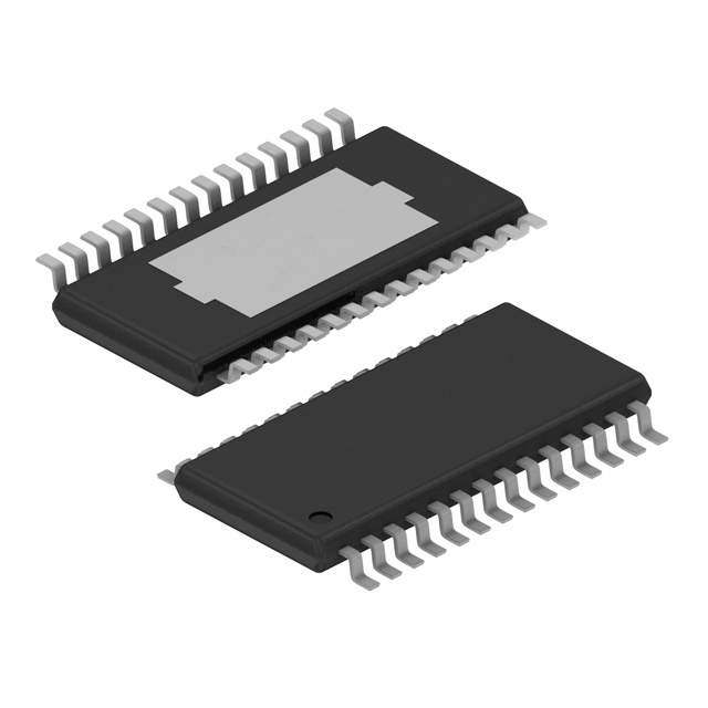
| 描述 | IC REG BUCK SYNC ADJ 6A 28HTSSOP稳压器—开关式稳压器 6A Sync Buck Converter |
| 产品分类 | |
| 品牌 | Texas Instruments |
| 产品手册 | |
| 产品图片 |
|
| rohs | 符合RoHS无铅 / 符合限制有害物质指令(RoHS)规范要求 |
| 产品系列 | 电源管理 IC,稳压器—开关式稳压器,Texas Instruments TPS54673PWPSWIFT™ |
| 数据手册 | |
| 产品型号 | TPS54673PWP |
| PWM类型 | - |
| 产品培训模块 | http://www.digikey.cn/PTM/IndividualPTM.page?site=cn&lang=zhs&ptm=16804 |
| 产品目录页面 | |
| 产品种类 | 稳压器—开关式稳压器 |
| 供应商器件封装 | 28-HTSSOP |
| 其它名称 | 296-13828-5 |
| 制造商产品页 | http://www.ti.com/general/docs/suppproductinfo.tsp?distId=10&orderablePartNumber=TPS54673PWP |
| 包装 | 管件 |
| 单位重量 | 118.500 mg |
| 同步整流器 | 是 |
| 商标 | Texas Instruments |
| 安装类型 | 表面贴装 |
| 安装风格 | SMD/SMT |
| 宽度 | 4.4 mm |
| 封装 | Tube |
| 封装/外壳 | 28-SOIC(0.173",4.40mm 宽)裸露焊盘 |
| 封装/箱体 | HTSSOP-28 |
| 工作温度 | -40°C ~ 85°C |
| 工作温度范围 | - 40 C to + 85 C |
| 工厂包装数量 | 50 |
| 开关频率 | 700 kHz |
| 拓扑结构 | Buck |
| 最大工作温度 | + 85 C |
| 最大输入电压 | 6 V |
| 最小工作温度 | - 40 C |
| 最小输入电压 | 3 V |
| 标准包装 | 50 |
| 电压-输入 | 3 V ~ 6 V |
| 电压-输出 | 0.9 V ~ 4.5 V |
| 电流-输出 | 6A |
| 类型 | 降压(降压) |
| 系列 | TPS54673 |
| 负载调节 | 0.03 % / A |
| 输出数 | 1 |
| 输出电压 | 4.5 V |
| 输出电流 | 6 A |
| 输出端数量 | 1 Output |
| 输出类型 | 可调式 |
| 配用 | /product-detail/zh/TPS54673EVM/296-20598-ND/562084/product-detail/zh/XILINXPWR-082/296-17304-ND/684804 |
| 频率-开关 | 350kHz,550kHz |


- 商务部:美国ITC正式对集成电路等产品启动337调查
- 曝三星4nm工艺存在良率问题 高通将骁龙8 Gen1或转产台积电
- 太阳诱电将投资9.5亿元在常州建新厂生产MLCC 预计2023年完工
- 英特尔发布欧洲新工厂建设计划 深化IDM 2.0 战略
- 台积电先进制程称霸业界 有大客户加持明年业绩稳了
- 达到5530亿美元!SIA预计今年全球半导体销售额将创下新高
- 英特尔拟将自动驾驶子公司Mobileye上市 估值或超500亿美元
- 三星加码芯片和SET,合并消费电子和移动部门,撤换高东真等 CEO
- 三星电子宣布重大人事变动 还合并消费电子和移动部门
- 海关总署:前11个月进口集成电路产品价值2.52万亿元 增长14.8%


PDF Datasheet 数据手册内容提取
Typical Size 6,4 mm X 9,7 mm (cid:1)(cid:2)(cid:3)(cid:4)(cid:5)(cid:6)(cid:7)(cid:8) www.ti.com SLVS433A − SEPTEMBER 2002 − REVISED FEBRUARY 2005 (cid:8)(cid:9)(cid:10) (cid:1)(cid:11) (cid:6)(cid:9)(cid:10) (cid:12)(cid:13)(cid:2)(cid:14)(cid:1)(cid:15) (cid:6)(cid:9)(cid:16) (cid:11)(cid:14)(cid:1)(cid:2)(cid:14)(cid:1) (cid:3)(cid:17)(cid:13)(cid:18)(cid:19)(cid:20)(cid:11)(cid:13)(cid:11)(cid:14)(cid:3) (cid:21)(cid:14)(cid:18)(cid:22) (cid:3)(cid:23)(cid:12)(cid:1)(cid:18)(cid:19)(cid:24)(cid:20) (cid:23)(cid:12)(cid:1)(cid:19) (cid:25)(cid:12)(cid:3)(cid:16)(cid:21)(cid:26)(cid:24)(cid:25) (cid:3)(cid:12)(cid:13)(cid:22)(cid:12)(cid:13)(cid:27) (cid:25)(cid:14)(cid:20)(cid:12)(cid:13)(cid:27) (cid:3)(cid:1)(cid:16)(cid:20)(cid:1)(cid:9)(cid:14)(cid:2) FEATURES DESCRIPTION (cid:1) 30-mΩ, 12-A Peak MOSFET Switches for High Efficiency at 6-A Continuous Output Source As a member of the SWIFT family of dc/dc regulators, or Sink Current the TPS54673 low-input voltage high-output current (cid:1) Disabled Current Sinking During Start-Up synchronous buck PWM converter integrates all (cid:1) 0.9-V to 3.3-V Adjustable Output Voltage required active components. Included on the substrate Range With 1.0% Accuracy with the listed features are a true, high performance, (cid:1) Wide PWM Frequency: voltage error amplifier that enables maximum Fixed 350 kHz, 550 kHz or performance and flexibility in choosing the output filter Adjustable 280 kHz to 700 kHz L and C components; an under-voltage-lockout circuit (cid:1) to prevent start-up until the input voltage reaches 3 V; Synchronizable to 700 kHz an internally or externally set slow-start circuit to limit (cid:1) Load Protected by Peak Current Limit and in-rush currents; and a power good output useful for Thermal Shutdown processor/logic reset, fault signaling, and supply (cid:1) Integrated Solution Reduces Board Area and sequencing. Component Count For reliable power up in output precharge applications, APPLICATIONS the TPS54673 is designed to only source current during (cid:1) startup. Low-Voltage, High-Density Distributed Power Systems (cid:1) The TPS54673 is available in a thermally enhanced Point of Load Regulation for High 28-pin TSSOP (PWP) PowerPAD package, which Performance DSPs, FPGAs, ASICs and eliminates bulky heatsinks. TI provides evaluation Microprocessors modules and the SWIFT designer software tool to aid (cid:1) Broadband, Networking and Optical in quickly achieving high-performance power supply Communications Infrastructure designs to meet aggressive equipment development (cid:1) Power PC Series Processors cycles. TYPICAL APPLICATION START UP WAVEFORM * * RL = 2 Ω I/O Supply Core Supply VIN PH TPS54673 BOOT VI = 3.3 V PGND div VBIAS VSENSE 1 V/ AGNDCOMP VO = 2.5 V * Optional 5.0 ms/div Please be aware that an important notice concerning availability, standard warranty, and use in critical applications of TexasInstruments semiconductor products and disclaimers thereto appears at the end of this data sheet. PowerPAD and SWIFT are trademarks of Texas Instruments. (cid:2)(cid:20)(cid:11)(cid:25)(cid:14)(cid:18)(cid:1)(cid:12)(cid:11)(cid:13) (cid:25)(cid:16)(cid:1)(cid:16) (cid:28)(cid:29)(cid:30)(cid:31)!"#$(cid:28)(cid:31)(cid:29) (cid:28)% &’!!((cid:29)$ #% (cid:31)(cid:30) )’*+(cid:28)&#$(cid:28)(cid:31)(cid:29) ,#$(- (cid:2)!(cid:31),’&$% Copyright 2002 − 2005, Texas Instruments Incorporated &(cid:31)(cid:29)(cid:30)(cid:31)!" $(cid:31) %)(&(cid:28)(cid:30)(cid:28)&#$(cid:28)(cid:31)(cid:29)% )(! $.( $(!"% (cid:31)(cid:30) (cid:1)(/#% (cid:12)(cid:29)%$!’"((cid:29)$% %$#(cid:29),#!, 0#!!#(cid:29)$1- (cid:2)!(cid:31),’&$(cid:28)(cid:31)(cid:29) )!(cid:31)&(%%(cid:28)(cid:29)2 ,(cid:31)(% (cid:29)(cid:31)$ (cid:29)(&(%%#!(cid:28)+1 (cid:28)(cid:29)&+’,( $(%$(cid:28)(cid:29)2 (cid:31)(cid:30) #++ )#!#"($(!%-
(cid:1)(cid:2)(cid:3)(cid:4)(cid:5)(cid:6)(cid:7)(cid:8) www.ti.com SLVS433A − SEPTEMBER 2002 − REVISED FEBRUARY 2005 These devices have limited built-in ESD protection. The leads should be shorted together or the device placed in conductive foam during storage or handling to prevent electrostatic damage to the MOS gates. ORDERING INFORMATION TA OUTPUT VOLTAGE PACKAGE PART NUMBER −40°C to 85°C 0.9 V to 3.3 V Plastic HTSSOP (PWP)(1) TPS54673PWP (1)The PWP package is also available taped and reeled. Add an R suffix to the device type (i.e., TPS54673PWPR). See the application section of the data sheet for PowerPAD drawing and layout information. (2)For the most current package and ordering information, see the Package Option Addendum at the end of this document, or see the TI website at www.ti.com. ABSOLUTE MAXIMUM RATINGS over operating free-air temperature range unless otherwise noted(1) TPS54673 VIN, SS/ENA, SYNC −0.3 V to 7 V RT −0.3 V to 6 V IInnppuutt vvoollttaaggee rraannggee,, VVII VSENSE −0.3 V to 4V BOOT −0.3 V to 17 V VBIAS, COMP, PWRGD −0.3 V to 7 V OOuuttppuutt vvoollttaaggee rraannggee,, VVOO PH −0.6 V to 10 V PH Internally limited SSoouurrccee ccuurrrreenntt,, IIOO COMP, VBIAS 6 mA PH 12 A SSiinnkk ccuurrrreenntt,, IISS COMP 6 mA SS/ENA, PWRGD 10 mA Voltage differential AGND to PGND ±0.3 V Operating virtual junction temperature range, TJ −40°C to 125°C Storage temperature, Tstg −65°C to 150°C Lead temperature 1,6 mm (1/16 inch) from case for 10 seconds 300°C (1)Stresses beyond those listed under “absolute maximum ratings” may cause permanent damage to the device. These are stress ratings only, and functional operation of the device at these or any other conditions beyond those indicated under “recommended operating conditions” is not implied. Exposure to absolute-maximum-rated conditions for extended periods may affect device reliability. RECOMMENDED OPERATING CONDITIONS MIN NOM MAX UNIT Input voltage, VI 3 6 V Operating junction temperature, TJ −40 125 °C DISSIPATION RATINGS(1)(2) THERMAL IMPEDANCE TA =25°C TA = 70°C TA = 85°C PACKAGE JUNCTION-TO-AMBIENT POWER RATING POWER RATING POWER RATING 28 Pin PWP with solder 18.2 °C/W 5.49 W(3) 3.02 W 2.20 W 28 Pin PWP without solder 40.5 °C/W 2.48 W 1.36 W 0.99 W (1)For more information on the PWP package, refer to TI technical brief, literature number SLMA002. (2)Test board conditions: 1. 3” x 3”, 4 layers, thickness: 0.062” 2. 1.5 oz. copper traces located on the top of the PCB 3. 1.5 oz. copper ground plane on the bottom of the PCB 4. 0.5 oz. copper ground planes on the 2 internal layers 5. 12 thermal vias (see “Recommended Land Pattern” in applications section of this data sheet) (3)Maximum power dissipation may be limited by over current protection. 2
(cid:1)(cid:2)(cid:3)(cid:4)(cid:5)(cid:6)(cid:7)(cid:8) www.ti.com SLVS433A − SEPTEMBER 2002 − REVISED FEBRUARY 2005 ELECTRICAL CHARACTERISTICS TJ = −40°C to 125°C, VI = 3 V to 6 V (unless otherwise noted) PARAMETER TEST CONDITIONS MIN TYP MAX UNIT SUPPLY VOLTAGE, VIN Input voltage range, VIN 3.0 6.0 V fs = 350 kHz, SYNC≤ 0.8 V, RT open, 11 15.8 PH pin open I(Q) Quiescent current fs = 550 kHz, SYNC≥ 2.5 V, RT open, 16 23.5 mA PH pin open Shutdown, SS/ENA = 0 V 1 1.4 UNDER VOLTAGE LOCK OUT Start threshold voltage, UVLO 2.95 3.0 V Stop threshold voltage, UVLO 2.70 2.80 V Hysteresis voltage, UVLO 0.14 0.16 V Rising and falling edge deglitch, UVLO(1) 2.5 µs BIAS VOLTAGE Output voltage, VBIAS I(VBIAS) = 0 2.70 2.80 2.90 V Output current, VBIAS (2) 100 µA CUMULATIVE REFERENCE Vref Accuracy 0.882 0.891 0.900 V REGULATION LLiinnee rreegguullaattiioonn((11))((33)) IL = 3 A, fs = 350 kHz, TJ = 85°C 0.04 %%//VV IL = 3 A, fs = 550 kHz, TJ = 85°C 0.04 LLooaadd rreegguullaattiioonn((11))((33)) IL = 0 A to 6 A, fs = 350 kHz, TJ = 85°C 0.03 %%//AA IL = 0 A to 6 A, fs = 550 kHz, TJ = 85°C 0.03 OSCILLATOR SYNC ≤ 0.8 V, RT open 280 350 420 IInntteerrnnaallllyy sseett——ffrreeee rruunnnniinngg ffrreeqquueennccyy kkHHzz SYNC ≥ 2.5 V, RT open 440 550 660 RT = 180 kΩ (1% resistor to AGND) 252 280 308 EExxtteerrnnaallllyy sseett——ffrreeee rruunnnniinngg ffrreeqquueennccyy rraannggee RT = 100 kΩ (1% resistor to AGND) 460 500 540 kkHHzz RT = 68 kΩ (1% resistor to AGND) 663 700 762 High level threshold, SYNC 2.5 V Low level threshold, SYNC 0.8 V Pulse duration, external synchronization, SYNC(1) 50 ns Frequency range, SYNC(1) 330 700 kHz Ramp valley(1) 0.75 V Ramp amplitude (peak-to-peak)(1) 1 V Minimum controllable on time(1) 200 ns Maximum duty cycle 90% (1)Specified by design (2)Static resistive loads only (3)Specified by the circuit used in Figure 10 3
(cid:1)(cid:2)(cid:3)(cid:4)(cid:5)(cid:6)(cid:7)(cid:8) www.ti.com SLVS433A − SEPTEMBER 2002 − REVISED FEBRUARY 2005 ELECTRICAL CHARACTERISTICS (continued) TJ = −40°C to 125°C, VI = 3 V to 6 V (unless otherwise noted) PARAMETER TEST CONDITIONS MIN TYP MAX UNIT ERROR AMPLIFIER Error amplifier open loop voltage gain 1 kΩ COMP to AGND(1) 90 110 dB Error amplifier unity gain bandwidth Parallel 10 kΩ, 160 pF COMP to AGND(1) 3 5 MHz Error amplifier common mode input voltage range Powered by internal LDO(1) 0 VBIAS V Input bias current, VSENSE VSENSE = Vref 60 250 nA Output voltage slew rate (symmetric), COMP 1.0 1.4 V/µs PWM COMPARATOR PWM comparator propagation delay time, PWM comparator input to PH pin (excluding 10-mV overdrive(1) 70 85 ns deadtime) SLOW-START/ENABLE Enable threshold voltage, SS/ENA 0.82 1.20 1.40 V Enable hysteresis voltage, SS/ENA 0.03 V Falling edge deglitch, SS/ENA(1) 2.5 µs Internal slow-start time 2.6 3.35 4.1 ms Charge current, SS/ENA SS/ENA = 0 V 3 5 8 µA Discharge current, SS/ENA SS/ENA = 1.3 V, VI = 1.5 V 2.0 2.3 4.0 mA POWER GOOD Power good threshold voltage VSENSE falling 90 %Vref Power good hysteresis voltage(1) 3 %Vref Power good falling edge deglitch(1) 35 µs Output saturation voltage, PWRGD I(sink) = 2.5 mA 0.18 0.3 V Leakage current, PWRGD VI = 5.5 V 1 µA CURRENT LIMIT VI = 3 V Output shorted(1) 7.2 10 CCuurrrreenntt lliimmiitt ttrriipp ppooiinntt AA VI = 6 V Output shorted(1) 10 12 Current limit leading edge blanking time 100 ns Current limit total response time 200 ns THERMAL SHUTDOWN Thermal shutdown trip point(1) 135 150 165 °C Thermal shutdown hysteresis(1) 10 °C OUTPUT POWER MOSFETS VI = 6 V(4) 26 47 rrDDSS((oonn)) PPoowweerr MMOOSSFFEETT sswwiittcchheess VI = 3 V(4) 36 65 mmΩΩ (1)Specified by design (2)Static resistive loads only (3)Specified by the circuit used in Figure 10 (4)Matched MOSFETs low-side rDS(on) production tested, high-side rDS(on) specified by design 4
(cid:1)(cid:2)(cid:3)(cid:4)(cid:5)(cid:6)(cid:7)(cid:8) www.ti.com SLVS433A − SEPTEMBER 2002 − REVISED FEBRUARY 2005 PWP PACKAGE (TOP VIEW) AGND 1 28 RT VSENSE 2 27 SYNC COMP 3 26 SS/ENA PWRGD 4 25 VBIAS BOOT 5 24 VIN PH 6 23 VIN PH 7 THERMAL 22 VIN PH 8 PAD 21 VIN PH 9 20 VIN PH 10 19 PGND PH 11 18 PGND PH 12 17 PGND PH 13 16 PGND PH 14 15 PGND TERMINAL FUNCTIONS TERMINAL DDEESSCCRRIIPPTTIIOONN NAME NO. AGND 1 Analog ground. Return for compensation network/output divider, slow-start capacitor, VBIAS capacitor, RT resistor and SYNC pin. Connect PowerPAD to AGND. BOOT 5 Bootstrap output. 0.022-µF to 0.1-µF low-ESR capacitor connected from BOOT to PH generates floating drive for the high-side FET driver. COMP 3 Error amplifier output. Connect frequency compensation network from COMP to VSENSE PGND 15−19 Power ground. High current return for the low-side driver and power MOSFET. Connect PGND with large copper areas to the input and output supply returns, and negative terminals of the input and output capacitors. A single point connection to AGND is recommended. PH 6−14 Phase output. Junction of the internal high-side and low-side power MOSFETs, and output inductor. PWRGD 4 Power good open drain output. High when VSENSE ≥ 90% Vref, otherwise PWRGD is low. Note that output is low when SS/ENA is low, or the internal shutdown signal is active. RT 28 Frequency setting resistor input. Connect a resistor from RT to AGND to set the switching frequency. When using the SYNC pin, set the RT value for a frequency at or slightly lower than the external oscillator frequency. SS/ENA 26 Slow-start/enable input/output. Dual function pin which provides logic input to enable/disable device operation and capacitor input to externally set the start-up time. SYNC 27 Synchronization input. Dual function pin which provides logic input to synchronize to an external oscillator or pin select between two internally set switching frequencies. When used to synchronize to an external signal, a resistor must be connected to the RT pin. VBIAS 25 Internal bias regulator output. Supplies regulated voltage to internal circuitry. Bypass VBIAS pin to AGND pin with a high quality, low-ESR 0.1-µF to 1.0-µF ceramic capacitor. VIN 20−24 Input supply for the power MOSFET switches and internal bias regulator. Bypass VIN pins to PGND pins close to device package with a high quality, low-ESR 10-µF ceramic capacitor. VSENSE 2 Error amplifier inverting input. Connect to output voltage through compensation network/output divider. 5
(cid:1)(cid:2)(cid:3)(cid:4)(cid:5)(cid:6)(cid:7)(cid:8) www.ti.com SLVS433A − SEPTEMBER 2002 − REVISED FEBRUARY 2005 INTERNAL BLOCK DIAGRAM AGND VBIAS VIN Enable Comparator SS/ENA VBIAS REG Falling SHUTDOWN 1.2 V Edge ILIM VIN Deglitch Thermal Comparator 3 − 6 V Hysteresis: 0.03 2.5 µs Shutdown Leading V 150°C Edge VIN UVLO Blanking Comparator Faalnlidng 100 ns SHUTDOWN VIN BOOT Rising 2.95 V Edge Hysteresis: 0.16 Deglitch Start-Up 30 mΩ V 2.5 µs SS_DIS Driver Suppression PH LOUT VO Internal/External Slow-start + (Internal Slow-Start Time = 3.35 ms − R Q Adaptive Dead-Time CO and Error S Control Logic Amplifier PWM Reference Comparator VIN VREF = 0.891 V 30 mΩ OSC PGND Powergood Comparator PWRGD VSENSE Falling 0.90 Vref Edge TPS54673 Deglitch Hysteresis: 0.03 Vref SHUTDOWN 35 µs VSENSE COMP RT SYNC ADDITIONAL 6A SWIFT DEVICES, (REFER TO SLVS397 AND SLVS400) DEVICE OUTPUT VOLTAGE DEVICE OUTPUT VOLTAGE DEVICE OUTPUT VOLTAGE TPS54611 0.9 V TPS54614 1.8 V TPS54672 Active termination TPS54612 1.2 V TPS54615 2.5 V TPS54610 Adjustable TPS54613 1.5 V TPS54616 3.3 V TPS54680 Sequencing RELATED DC/DC PRODUCTS (cid:1) TPS54873 − DC/DC Converter (Integrated Switch) (cid:1) TPS40000 − DC/DC Controller (cid:1) TPS40002 − DC/DC Controller 6
(cid:1)(cid:2)(cid:3)(cid:4)(cid:5)(cid:6)(cid:7)(cid:8) www.ti.com SLVS433A − SEPTEMBER 2002 − REVISED FEBRUARY 2005 TYPICAL CHARACTERISTICS DRAIN-SOURCE DRAIN-SOURCE INTERNALLY SET ON-STATE RESISTANCE ON-STATE RESISTANCE OSCILLATOR FREQUENCY vs vs vs JUNCTION TEMPERATURE JUNCTION TEMPERATURE JUNCTION TEMPERATURE ΩDrain Source On-State Reststance − m 1234560000000−40VIN = 3.03 V 25 IO = 6 8A5 125 ΩDrain Source On-State Reststance − m 1234560000000−40VIN = 5 0V 25IO = 6 A85 125 f − Internally Set Oscillator Frequency − kHz 234567555555000000−40 SSYYNNCC 0 ≤≥ 02..85 VV 25 85 125 TJ − Junction Temperature − °C TJ − Junction Temperature − °C TJ − Junction Temperature − °C Figure 1 Figure 2 Figure 3 OSCEILXLTAETRONRA FLRLYE QSUEETNCY VOLTAGE REFERENCE DEVICE POWER LOSSES AT TJ = 125°C vs vs vs LOAD CURRENT JUNCTION TEMPERATURE JUNCTION TEMPERATURE y − kHz 800 0.895 4.55 TfsJ = = 7 10205 k°CHz nc 700 V 0.893 W 4 cillator Freque 560000 RT = 68 k e Reference − 0.891 wer Losses − 23..553 VI = 3.3 V Externally Set Os 340000 RRTT == 110800 kk − VoltagVref00..888879 Device Po 01..5512 VI = 5 V f − 200−40 0 25 85 125 0.885−40 0 25 85 125 00 1 2 3 4 5 6 7 8 TJ − Junction Temperature − °C TJ − Junction Temperature − °C IL − Load Current − A Figure 4 Figure 5 Figure 6 OUTPUT VOLTAGE REGULATION INTERNAL SLOW-START TIME ERROR AMPLIFIER vs vs OPEN LOOP RESPONSE INPUT VOLTAGE JUNCTION TEMPERATURE 0.895 140 0 3.80 V TA = 85°C, RL = 10 kΩ, −20 − Output Voltage Regulation − O0000....888888997913 IO = 3 A fs = 550 kHz Gain − dB11022468000000 GPahCTianALs e== 2156°0C pF, −−−−−−−111186464200000000Phase − Degrees nternal Slow-Start Time − ms 33333.....0235650505 V 0 −180 I 2.90 0.885 −20 −200 2.75 3 3.5 4 4.5 5 5.5 6 1 10 100 1 k 10 k 100 k 1 M 10 M −40 0 25 85 125 VI − Input Voltage − V f − Frequency − Hz TJ − Junction Temperature − °C Figure 7 Figure 8 Figure 9 7
(cid:1)(cid:2)(cid:3)(cid:4)(cid:5)(cid:6)(cid:7)(cid:8) www.ti.com SLVS433A − SEPTEMBER 2002 − REVISED FEBRUARY 2005 APPLICATION INFORMATION Figure 10 shows the schematic diagram for a typical is set at 2.5 V and the input voltage is 3.3 V. For proper TPS54673 application. The TPS54673 (U1) can provide operation, the PowerPAD underneath the integrated up to 6 A of output current at a nominal output voltage of circuit TPS54673 must be soldered properly to the 0.9 V to 3.3 V, and for this application, the output voltage printed-circuit board. U1 TPS54673 R6 28 24 RT VIN VIN 71.5 kΩ 27 VIN 2232 C10 C12 3.3 V SYNCH VIN 21 10 µF 10 µF VIN C6 26 20 SS/ENA VIN 14 0.047 µF PH C3 25 VBIAS PH 13 1 µF R5 10 kΩ 4 PH 1112 VIN PWRGD PH 10 R1 R3 PH C4 3 9 COMP PH 10 kΩ 10 kΩ 470 pF PH 8 7 PH C1 R2 C2 12 pF 6 PH 470 pF 301 Ω 2 VSENSE BOOT 5 C9 1D 1A, 200 V PGND 19 0.047 µF R4 PGND 18 5.49 kΩ 17 PGND 1 A, 200 V 1 16 D2 AGND PGND 15 PGND PwrPad VOUT 2.5 V R7 C13 C5 C7 C8 L1 2.4 kΩ 0.1 µF 22 µF 22 µF 22 µF 0.65 µH C11 3300 pF Figure 10. Application Circuit COMPONENT SELECTION the input supply, must be located as close as possible to the device. Ripple current is carried in both C10 and C12, The values for the components used in this design and the return path to PGND should avoid the current example are selected for low output ripple and small PCB circulating in the output capacitors C5, C7, C8 and C13. area. Ceramic capacitors are utilized in the output filter circuit. A small size, small value output inductor is also used. Compensation network components are chosen to FEEDBACK CIRCUIT maximize closed loop bandwidth and provide good transient response characteristics. Additional design The values for these components are selected to provide information is available at www.ti.com. fast transient response times. R1, R2, R3, R4, C1, C2, and C4 forms the loop-compensation network for the circuit. INPUT VOLTAGE For this design, a Type 3 topology is used. The transfer function of the feedback network is chosen to provide The input voltage is a nominal 3.3 VDC. The input filter maximum closed loop gain available with open loop (C12) is a 10-µF ceramic capacitor (Taiyo Yuden). C10, characteristics of the internal error amplifier. Closed loop also a 10-µF ceramic capacitor (Taiyo Yuden) that crossover frequency is typically between 80 kHz at 3.3 V provides high frequency decoupling of the TPS54673 from input. 8
(cid:1)(cid:2)(cid:3)(cid:4)(cid:5)(cid:6)(cid:7)(cid:8) www.ti.com SLVS433A − SEPTEMBER 2002 − REVISED FEBRUARY 2005 OPERATING FREQUENCY signals. Noise injected between the two grounds can degrade the performance of the TPS54673, particularly at In the application circuit, the RT pin is grounded through a higher output currents. Ground noise on an analog ground 71.5-kΩ resistor (R6) to select the operating frequency of plane can also cause problems with some of the control 700 kHz. To set a different frequency, place a 68-kΩ to and bias signals. For these reasons, separate analog and 180-kΩ resistor between RT (pin 28) and analog ground or power ground traces are recommended. There should be leave RT floating to select the default of 350 kHz. The an area of ground on the top layer directly under the IC, resistance can be approximated using the following with an exposed area for connection to the PowerPAD. equation: Use vias to connect this ground area to any internal ground plane. Use additional vias at the ground side of the input R(cid:1) 500kHz (cid:2)100[k(cid:1)] and output filter capacitors as well. The AGND and PGND SwitchingFrequency (1) pins should be tied to the PCB ground by connecting them to the ground area under the device as shown. The only components that should tie directly to the power ground OUTPUT FILTER plane are the input capacitors, the output capacitors, the input voltage decoupling capacitor, and the PGND pins of The output filter is composed of a 0.65-µH inductor (L1) the TPS54673. Use a separate wide trace for the analog and 3 x 22-µF capacitors (C5, C7 and C8). The inductor is ground signal path. This analog ground should be used for a low dc resistance (.017 Ω) type, Pulse PA0277 0.65 µH. the voltage set point divider, timing resistor RT, slow start The capacitors used are 22-µF, 6.3-V ceramic types with capacitor, and bias capacitor grounds. Connect this trace X5R dielectric. An additional high frequency bypass directly to AGND (Pin 1). capacitor, C13 is also used. The PH pins should be tied together and routed to the PRECHARGE CIRCUIT output inductor. Since the PH connection is the switching node, the inductor should be located very close to the PH VIN precharges the output of the application circuit pins and the area of the PCB conductor minimized to through series diodes (D1 and D2) during start-up. As prevent excessive capacitive coupling. the input voltage increases at start-up, the output is precharged to VIN minus the forward bias voltage of the two diodes. When the internal reference has ramped up Connect the boot capacitor between the phase node and to a value greater than the voltage fed back to the the BOOT pin as shown. Keep the boot capacitor close to VSENSE pin, the output of the internal error amplifier the IC and minimize the conductor trace lengths. begins to increase. When this output reaches the maximum ramp amplitude, the output of the PWM Connect the output filter capacitor(s) as shown between comparator reaches 100 percent duty cycle and the the VOUT trace and PGND. It is important to keep the loop internal logic enables the high-side FET driver and formed by the PH pins, Lout, Cout and PGND as small as switching begins. The output tracks the internal practical. reference until the preset output voltage is reached. Under no circumstances should the precharge voltage Place the compensation components from the VOUT trace be allowed to increase above the preset output value. to the VSENSE and COMP pins. Do not place these components too close to the PH trace. Due to the size of PCB LAYOUT the IC package and the device pinout, the components will have to be routed somewhat close, but maintain as much Figure 11 details a generalized PCB layout guide for the separation as possible while still keeping the layout TPS54673. The VIN pins should be connected together on compact. the printed circuit board (PCB) and bypassed with a low ESR ceramic bypass capacitor. Care should be taken to Connect the bias capacitor from the VBIAS pin to analog minimize the loop area formed by the bypass capacitor ground using the isolated analog ground trace. If a connections, the VIN pins, and the TPS54673 ground slow−start capacitor or RT resistor is used, or if the SYNC pins. The minimum recommended bypass capacitance is pin is used to select 350 kHz operating frequency, connect 10 µF ceramic with a X5R or X7R dielectric and the them to this trace as well. optimum placement is closest to the VIN pins and the PGND pins. If pre−charge diodes are used, keep the path from the The TPS54673 has two internal grounds (analog and voltage source to the output filter capacitor short. Make power). The analog ground ties to all of the noise sensitive sure the etch is wide enough to carry the pre−charge signals, while the power ground ties to the noisier power current. 9
(cid:1)(cid:2)(cid:3)(cid:4)(cid:5)(cid:6)(cid:7)(cid:8) www.ti.com SLVS433A − SEPTEMBER 2002 − REVISED FEBRUARY 2005 OPTIONAL PRE−CHARGE DIODES ANALOG GROUND TRACE FREQUENCY SET RESISTOR AGND RT VSENSE SYNC SLOW START CAPACITOR COMPENSATION COMP SS/ENA NETWORK BIAS CAPACITOR PWRGD VBIAS BOOT CAPACITOR BOOT VIN EXPOSED PH POWERPAD VIN VOUT AREA PH VIN PH VIN VIN PH PH VIN PH PGND OUTPUT INDUCTOR PH PGND OUTPUT PH PGND FILTER CAPACITOR PH PGND INPUT INPUT PH PGND BYPASS BULK CAPACITOR FILTER TOPSIDE GROUND AREA VIA to Ground Plane Figure 11. TPS54673 PCB Layout 10
(cid:1)(cid:2)(cid:3)(cid:4)(cid:5)(cid:6)(cid:7)(cid:8) www.ti.com SLVS433A − SEPTEMBER 2002 − REVISED FEBRUARY 2005 LAYOUT CONSIDERATIONS FOR THERMAL any area available should be used when 6 A or greater PERFORMANCE operation is desired. Connection from the exposed area of the PowerPAD to the analog ground plane layer should be For operation at full rated load current, the analog ground made using 0.013 inch diameter vias to avoid solder plane must provide adequate heat dissipating area. A 3 wicking through the vias. Eight vias should be in the inch by 3 inch plane of 1 ounce copper is recommended, PowerPAD area with four additional vias located under the though not mandatory, depending on ambient temperature device package. The size of the vias under the package, and airflow. Most applications have larger areas of internal but not in the exposed thermal pad area, can be increased ground plane available, and the PowerPAD should be to 0.018. Additional vias beyond the ten recommended connected to the largest area available. Additional areas that enhance thermal performance should be included in on the top or bottom layers also help dissipate heat, and areas not under the device package. Minimum Recommended Thermal Vias: 8 x 0.013 Diameter Inside 8 PL Ø0.0130 Powerpad Area 4 x 0.018 Diameter Under Device as Shown. Additional 0.018 Diameter Vias May Be Used if Top Side Analog Ground 4 PL Ø0.0180 Area Is Extended. Connect Pin 1 to Analog Ground Plane in This Area for Optimum Performance 0.0150 0.06 0.0339 0.0650 0.0500 0.3820 0.3478 0.0500 0.2090 0.0500 0.0256 0.0650 0.0339 Minimum Recommended Exposed Copper Area for Powerpad. 5-mm 0.1700 Stencils May Require 10 Percent 0.1340 Larger Area Minimum Recommended Top Side Analog Ground Area 0.0630 0.0400 Figure 12. Recommended Land Pattern for 28-Pin PWP PowerPAD PERFORMANCE GRAPHS Data shown is for the circuit in Figure 10 with precharge disabled (D1 and D2 removed) except for slow-start timing of Figure 19. All data is for VI = 3.3 V, VO = 2.5 V, fs = 700 kHz and TA = 25°C, unless otherwise specified. EFFICIENCY OUTPUT VOLTAGE OUTPUT VOLTAGE vs vs vs OUTPUT CURRENT OUTPUT CURRENT INPUT VOLTAGE 100 2.52 2.52 95 VI = 3.3 V, VO = 2.5 V 2.515 2.515 VI = 3.3 V 90 V Efficiency − % 6778850505 VI = 5 V, VO = 2.5 V − Output Voltage − O22..245.2905.5515 VI = 5 V − Output Voltage − V 22..245.2905.5515 V 2.49 O 2.49 60 V IO = 3 A 2.485 2.485 55 50 2.48 2.48 0 1 2 3 4 5 6 7 0 1 2 3 4 5 6 7 3 3.5 4 4.5 5 5.5 6 IO − Output Current − A IO − Output Current − A VI − Input Voltage − V Figure 13 Figure 14 Figure 15 11
(cid:1)(cid:2)(cid:3)(cid:4)(cid:5)(cid:6)(cid:7)(cid:8) www.ti.com SLVS433A − SEPTEMBER 2002 − REVISED FEBRUARY 2005 AMBIENT TEMPERATURE vs LOOP RESPONSE LOAD CURRENT OUTPUT RIPPLE VOLTAGE 125 6500 118500 115 TJ = 125°C v Gain − dB−−1423210000000 Phase Gain −31690−020063000Phase − Degrees °Ambient Temperature − C 104567895555555 Safe Operating Area(1V)I = 3.3 VVI = 5 V utput Ripple Voltage − 10 mV/di O −30 −90 35 −40 −120 25 100 1 k 10 k 100 k 1 M 0 1 2 3 4 5 6 7 8 Time − 1 µs/div f − Frequency − Hz IO − Output Current − A Figure 16 Figure 17 Figure 18 LOAD TRANSIENT RESPONSE SLOW-START TIMING I = 1.5 A to 4.5 A RL = 2 Ω VI = 3.3 V v mV/di V/div 0 1 5 v di VO = 2.5 V A/ 2 100 µs/div 5.0 ms/div Figure 19 Figure 20 (1)Safe operating area is applicable to the test board conditions in the Dissipation Ratings DETAILED DESCRIPTION threshold voltage of 2.95 V. Once the UVLO start threshold is reached, device start-up begins. The device operates DISABLED SINKING DURING START-UP until VIN falls below the nominal UVLO stop threshold of (DSDS) 2.8 V. Hysteresis in the UVLO comparator and a 2.5-µs The DSDS feature enables minimal voltage drooping of rising and falling edge deglitch circuit reduce the likelihood output precharge capacitors at start-up. The TPS54673 is of shutting the device down due to noise on VIN. designed to disable the low-side MOSFET to prevent sinking current from a precharge output capacitor during SLOW-START/ENABLE (SS/ENA) start-up. Once the high-side MOSFET has been turned on The slow-start/enable pin provides two functions. First, the to the maximum duty cycle limit, the low-side MOSFET is pin acts as an enable (shutdown) control by keeping the allowed to switch. Once the maximum duty cycle condition device turned off until the voltage exceeds the start is met, the converter functions as a sourcing converter until threshold voltage of approximately 1.2 V. When SS/ENA the SS/ENA is pulled low. exceeds the enable threshold, device start-up begins. The reference voltage fed to the error amplifier is linearly UNDERVOLTAGE LOCK OUT (UVLO) ramped up from 0 V to 0.891 V in 3.35 ms. Similarly, the The TPS54673 incorporates an under voltage lockout converter output voltage reaches regulation in circuit to keep the device disabled when the input voltage approximately 3.35 ms. Voltage hysteresis and a 2.5-µs (VIN) is insufficient. During power up, internal circuits are falling edge deglitch circuit reduce the likelihood of held inactive until VIN exceeds the nominal UVLO triggering the enable due to noise. 12
(cid:1)(cid:2)(cid:3)(cid:4)(cid:5)(cid:6)(cid:7)(cid:8) www.ti.com SLVS433A − SEPTEMBER 2002 − REVISED FEBRUARY 2005 The second function of the SS/ENA pin provides an externally adjusted from 280 to 700 kHz by connecting a external means of extending the slow-start time with a resistor between the RT pin and AGND and floating the low-value capacitor connected between SS/ENA and SYNC pin. The switching frequency is approximated by AGND. the following equation, where R is the resistance from RT to AGND: Adding a capacitor to the SS/ENA pin has two effects on start-up. First, a delay occurs between release of the SwitchingFrequency(cid:1)100k(cid:1)(cid:2)500[kHz] (4) SS/ENA pin and start-up of the output. The delay is R proportional to the slow-start capacitor value and lasts External synchronization of the PWM ramp is possible until the SS/ENA pin reaches the enable threshold. The over the frequency range of 330 kHz to 700 kHz by driving start-up delay is approximately: a synchronization signal into SYNC and connecting a 1.2 V (2) resistor from RT to AGND. Choose a resistor between the td(cid:1)C(SS)(cid:2) 5 (cid:2)A RT and AGND which sets the free running frequency to 80% of the synchronization signal. The following table Second, as the output becomes active, a brief ramp-up at summarizes the frequency selection configurations: the internal slow-start rate may be observed before the SWITCHING SYNC PIN RT PIN externally set slow-start rate takes control and the output FREQUENCY rises at a rate proportional to the slow-start capacitor. The 350 kHz, internally Float or AGND Float slow-start time set by the capacitor is approximately: set t (cid:1)C (cid:2)0.7 V (3) 550 kHz, internally ≥2.5 V Float (SS) (SS) 5 (cid:2)A set Externally set 280 Float R = 180 kΩ to 68 kΩ The actual slow-start time is likely to be less than the above kHz to 700 kHz approximation due to the brief ramp-up at the internal rate. Externally Synchronization R = RT value for 80% The low side MOSFET is off during the slow-start synchronized signal of external synchro- sequence. frequency nization frequency VBIAS REGULATOR (VBIAS) ERROR AMPLIFIER The high performance, wide bandwidth, voltage error The VBIAS regulator provides internal analog and digital amplifier sets the TPS54673 apart from most dc/dc blocks with a stable supply voltage over variations in converters. The user is given the flexibility to use a wide junction temperature and input voltage. A high quality, range of output L and C filter components to suit the low-ESR, ceramic bypass capacitor is required on the particular application needs. Type 2 or type 3 VBIAS pin. X7R or X5R grade dielectrics are compensation can be employed using external recommended because their values are more stable over compensation components. temperature. The bypass capacitor must be placed close to the VBIAS pin and returned to AGND. PWM CONTROL External loading on VBIAS is allowed, with the caution that Signals from the error amplifier output, oscillator, and internal circuits require a minimum VBIAS of 2.70V, and current limit circuit are processed by the PWM control external loads on VBIAS with ac or digital switching noise logic. Referring to the internal block diagram, the control may degrade performance. The VBIAS pin may be useful logic includes the PWM comparator, OR gate, PWM latch, as a reference voltage for external circuits. and portions of the adaptive dead-time and control logic block. During steady-state operation below the current VOLTAGE REFERENCE limit threshold, the PWM comparator output and oscillator The voltage reference system produces a precise Vref pulse train alternately reset and set the PWM latch. Once signal by scaling the output of a temperature stable the PWM latch is reset, the low-side FET remains on for a bandgap circuit. During manufacture, the bandgap and minimum duration set by the oscillator pulse width. During scaling circuits are trimmed to produce 0.891 V at the this period, the PWM ramp discharges rapidly to its valley output of the error amplifier, with the amplifier connected voltage. When the ramp begins to charge back up, the as a voltage follower. The trim procedure adds to the high low-side FET turns off and high-side FET turns on. As the precision regulation of the TPS54673, since it cancels PWM ramp voltage exceeds the error amplifier output offset errors in the scale and error amplifier circuits. voltage, the PWM comparator resets the latch, thus turning off the high-side FET and turning on the low-side OSCILLATOR AND PWM RAMP FET. The low-side FET remains on until the next oscillator The oscillator frequency can be set to internally fixed pulse discharges the PWM ramp. values of 350 kHz or 550 kHz using the SYNC pin as a During transient conditions, the error amplifier output static digital input. If a different frequency of operation is could be below the PWM ramp valley voltage or above the required for the application, the oscillator frequency can be PWM peak voltage. If the error amplifier is high, the PWM 13
(cid:1)(cid:2)(cid:3)(cid:4)(cid:5)(cid:6)(cid:7)(cid:8) www.ti.com SLVS433A − SEPTEMBER 2002 − REVISED FEBRUARY 2005 latch is never reset, and the high-side FET remains on until OVERCURRENT PROTECTION the oscillator pulse signals the control logic to turn the The cycle-by-cycle current limiting is achieved by sensing high-side FET off and the low-side FET on. The device the current flowing through the high-side MOSFET and operates at its maximum duty cycle until the output voltage comparing this signal to a preset overcurrent threshold. rises to the regulation set-point, setting VSENSE to The high side MOSFET is turned off within 200 ns of approximately the same voltage as VREF. If the error reaching the current limit threshold. A 100-ns leading edge amplifier output is low, the PWM latch is continually reset blanking circuit prevents current limit false tripping. and the high-side FET does not turn on. The low-side FET Current limit detection occurs only when current flows from remains on until the VSENSE voltage decreases to a VIN to PH when sourcing current to the output filter. Load range that allows the PWM comparator to change states. protection during current sink operation is provided by The TPS54673 is capable of sinking current continuously thermal shutdown. until the output reaches the regulation set-point. THERMAL SHUTDOWN If the current limit comparator trips for longer than 100 ns, the PWM latch resets before the PWM ramp exceeds the The device uses the thermal shutdown to turn off the power error amplifier output. The high-side FET turns off and MOSFETs and disable the controller if the junction low-side FET turns on to decrease the energy in the output temperature exceeds 150°C. The device is released from inductor and consequently the output current. This shutdown automatically when the junction temperature process is repeated each cycle in which the current limit decreases to 10°C below the thermal shutdown trip point, comparator is tripped. and starts up under control of the slow-start circuit. DEAD-TIME CONTROL AND MOSFET Thermal shutdown provides protection when an overload DRIVERS condition is sustained for several milliseconds. With a persistent fault condition, the device cycles continuously; Adaptive dead-time control prevents shoot-through starting up by control of the soft-start circuit, heating up due current from flowing in both N-channel power MOSFETs to the fault condition, and then shutting down upon during the switching transitions by actively controlling the reaching the thermal shutdown trip point. This sequence turnon times of the MOSFET drivers. The high-side driver repeats until the fault condition is removed. does not turn on until the voltage at the gate of the low-side FET is below 2 V. While the low-side driver does not turn POWER-GOOD (PWRGD) on until the voltage at the gate of the high-side MOSFET The power good circuit monitors for under voltage is below 2 V. conditions on VSENSE. If the voltage on VSENSE is 10% The high-side and low-side drivers are designed with below the reference voltage, the open-drain PWRGD 300-mA source and sink capability to quickly drive the output is pulled low. PWRGD is also pulled low if VIN is power MOSFETs gates. The low-side driver is supplied less than the UVLO threshold or SS/ENA is low, or a from VIN, while the high-side drive is supplied from the thermal shutdown occurs. When VIN ≥ UVLO threshold, BOOT pin. A bootstrap circuit uses an external BOOT SS/ENA ≥ enable threshold, and VSENSE > 90% of V , ref capacitor and an internal 2.5-Ω bootstrap switch the open drain output of the PWRGD pin is high. A connected between the VIN and BOOT pins. The hysteresis voltage equal to 3% of V and a 35 µs falling ref integrated bootstrap switch improves drive efficiency and edge deglitch circuit prevent tripping of the power good reduces external component count. comparator due to high frequency noise. 14
PACKAGE OPTION ADDENDUM www.ti.com 6-Feb-2020 PACKAGING INFORMATION Orderable Device Status Package Type Package Pins Package Eco Plan Lead/Ball Finish MSL Peak Temp Op Temp (°C) Device Marking Samples (1) Drawing Qty (2) (6) (3) (4/5) TPS54673PWP ACTIVE HTSSOP PWP 28 50 Green (RoHS NIPDAU Level-2-260C-1 YEAR -40 to 85 TPS54673 & no Sb/Br) TPS54673PWPR ACTIVE HTSSOP PWP 28 2000 Green (RoHS NIPDAU Level-2-260C-1 YEAR -40 to 85 TPS54673 & no Sb/Br) TPS54673PWPRG4 ACTIVE HTSSOP PWP 28 2000 Green (RoHS NIPDAU Level-2-260C-1 YEAR -40 to 85 TPS54673 & no Sb/Br) (1) The marketing status values are defined as follows: ACTIVE: Product device recommended for new designs. LIFEBUY: TI has announced that the device will be discontinued, and a lifetime-buy period is in effect. NRND: Not recommended for new designs. Device is in production to support existing customers, but TI does not recommend using this part in a new design. PREVIEW: Device has been announced but is not in production. Samples may or may not be available. OBSOLETE: TI has discontinued the production of the device. (2) RoHS: TI defines "RoHS" to mean semiconductor products that are compliant with the current EU RoHS requirements for all 10 RoHS substances, including the requirement that RoHS substance do not exceed 0.1% by weight in homogeneous materials. Where designed to be soldered at high temperatures, "RoHS" products are suitable for use in specified lead-free processes. TI may reference these types of products as "Pb-Free". RoHS Exempt: TI defines "RoHS Exempt" to mean products that contain lead but are compliant with EU RoHS pursuant to a specific EU RoHS exemption. Green: TI defines "Green" to mean the content of Chlorine (Cl) and Bromine (Br) based flame retardants meet JS709B low halogen requirements of <=1000ppm threshold. Antimony trioxide based flame retardants must also meet the <=1000ppm threshold requirement. (3) MSL, Peak Temp. - The Moisture Sensitivity Level rating according to the JEDEC industry standard classifications, and peak solder temperature. (4) There may be additional marking, which relates to the logo, the lot trace code information, or the environmental category on the device. (5) Multiple Device Markings will be inside parentheses. Only one Device Marking contained in parentheses and separated by a "~" will appear on a device. If a line is indented then it is a continuation of the previous line and the two combined represent the entire Device Marking for that device. (6) Lead/Ball Finish - Orderable Devices may have multiple material finish options. Finish options are separated by a vertical ruled line. Lead/Ball Finish values may wrap to two lines if the finish value exceeds the maximum column width. Important Information and Disclaimer:The information provided on this page represents TI's knowledge and belief as of the date that it is provided. TI bases its knowledge and belief on information provided by third parties, and makes no representation or warranty as to the accuracy of such information. Efforts are underway to better integrate information from third parties. TI has taken and continues to take reasonable steps to provide representative and accurate information but may not have conducted destructive testing or chemical analysis on incoming materials and chemicals. TI and TI suppliers consider certain information to be proprietary, and thus CAS numbers and other limited information may not be available for release. Addendum-Page 1
PACKAGE OPTION ADDENDUM www.ti.com 6-Feb-2020 In no event shall TI's liability arising out of such information exceed the total purchase price of the TI part(s) at issue in this document sold by TI to Customer on an annual basis. Addendum-Page 2
PACKAGE MATERIALS INFORMATION www.ti.com 12-Feb-2019 TAPE AND REEL INFORMATION *Alldimensionsarenominal Device Package Package Pins SPQ Reel Reel A0 B0 K0 P1 W Pin1 Type Drawing Diameter Width (mm) (mm) (mm) (mm) (mm) Quadrant (mm) W1(mm) TPS54673PWPR HTSSOP PWP 28 2000 330.0 16.4 6.9 10.2 1.8 12.0 16.0 Q1 PackMaterials-Page1
PACKAGE MATERIALS INFORMATION www.ti.com 12-Feb-2019 *Alldimensionsarenominal Device PackageType PackageDrawing Pins SPQ Length(mm) Width(mm) Height(mm) TPS54673PWPR HTSSOP PWP 28 2000 350.0 350.0 43.0 PackMaterials-Page2
GENERIC PACKAGE VIEW PWP 28 PowerPADTM TSSOP - 1.2 mm max height 4.4 x 9.7, 0.65 mm pitch SMALL OUTLINE PACKAGE Images above are just a representation of the package family, actual package may vary. Refer to the product data sheet for package details. 4224765/A www.ti.com
None
None
None
IMPORTANTNOTICEANDDISCLAIMER TI PROVIDES TECHNICAL AND RELIABILITY DATA (INCLUDING DATASHEETS), DESIGN RESOURCES (INCLUDING REFERENCE DESIGNS), APPLICATION OR OTHER DESIGN ADVICE, WEB TOOLS, SAFETY INFORMATION, AND OTHER RESOURCES “AS IS” AND WITH ALL FAULTS, AND DISCLAIMS ALL WARRANTIES, EXPRESS AND IMPLIED, INCLUDING WITHOUT LIMITATION ANY IMPLIED WARRANTIES OF MERCHANTABILITY, FITNESS FOR A PARTICULAR PURPOSE OR NON-INFRINGEMENT OF THIRD PARTY INTELLECTUAL PROPERTY RIGHTS. These resources are intended for skilled developers designing with TI products. You are solely responsible for (1) selecting the appropriate TI products for your application, (2) designing, validating and testing your application, and (3) ensuring your application meets applicable standards, and any other safety, security, or other requirements. These resources are subject to change without notice. TI grants you permission to use these resources only for development of an application that uses the TI products described in the resource. Other reproduction and display of these resources is prohibited. No license is granted to any other TI intellectual property right or to any third party intellectual property right. TI disclaims responsibility for, and you will fully indemnify TI and its representatives against, any claims, damages, costs, losses, and liabilities arising out of your use of these resources. TI’s products are provided subject to TI’s Terms of Sale (www.ti.com/legal/termsofsale.html) or other applicable terms available either on ti.com or provided in conjunction with such TI products. TI’s provision of these resources does not expand or otherwise alter TI’s applicable warranties or warranty disclaimers for TI products. Mailing Address: Texas Instruments, Post Office Box 655303, Dallas, Texas 75265 Copyright © 2020, Texas Instruments Incorporated