ICGOO在线商城 > 集成电路(IC) > PMIC - 稳压器 - DC DC 开关稳压器 > TPS5431DDA
 Datasheet下载
- 型号: TPS5431DDA
- 制造商: Texas Instruments
- 库位|库存: xxxx|xxxx
- 要求:
| 数量阶梯 | 香港交货 | 国内含税 |
| +xxxx | $xxxx | ¥xxxx |
查看当月历史价格
查看今年历史价格
TPS5431DDA产品简介:
ICGOO电子元器件商城为您提供TPS5431DDA由Texas Instruments设计生产,在icgoo商城现货销售,并且可以通过原厂、代理商等渠道进行代购。 TPS5431DDA价格参考¥13.96-¥25.95。Texas InstrumentsTPS5431DDA封装/规格:PMIC - 稳压器 - DC DC 开关稳压器, 可调式 降压 开关稳压器 IC 正 1.221V 1 输出 3A 8-PowerSOIC(0.154",3.90mm 宽)。您可以下载TPS5431DDA参考资料、Datasheet数据手册功能说明书,资料中有TPS5431DDA 详细功能的应用电路图电压和使用方法及教程。
TPS5431DDA 是德州仪器(Texas Instruments)推出的一款高效同步降压直流-直流(DC-DC)开关稳压器,适用于多种需要高性能电源管理的应用场景。以下是该型号的主要应用场景:

1. 通信设备:TPS5431DDA 可用于基站、路由器和交换机等通信设备中,为处理器、FPGA 和其他关键组件提供稳定的电源电压。其高效率和低功耗特性有助于减少热量生成,提高系统可靠性。

2. 工业自动化:在工业控制和自动化系统中,这款稳压器可以为可编程逻辑控制器(PLC)、数据采集系统(DAQ)以及传感器接口供电。其宽输入电压范围(4.5V 至 18V)使其能够适应各种工业电源环境。

3. 嵌入式计算:TPS5431DDA 适合为嵌入式计算机模块、单板计算机(SBC)和其他小型化计算平台供电。其紧凑的封装和高效的转换能力满足了空间受限的设计需求。

4. 消费电子:在高端消费电子产品中,如平板电脑、智能电视和游戏机,TPS5431DDA 提供稳定且高效的电源解决方案,支持快速启动和动态负载响应。

5. 医疗设备:对于便携式或台式医疗设备(如超声波机器、监护仪等),TPS5431DDA 的低电磁干扰(EMI)设计和高精度输出电压确保了设备的可靠性和安全性。

6. 汽车电子:尽管 TPS5431DDA 不是专门针对汽车级应用设计,但在非关键车载子系统中(如信息娱乐系统或导航模块),它仍可作为有效的电源管理方案。

总结来说,TPS5431DDA 凭借其出色的性能参数(如高达3A的连续输出电流、固定开关频率280kHz/550kHz可选、内置补偿功能等),成为众多需要高效、紧凑和可靠电源解决方案领域的理想选择。
| 参数 | 数值 |
| 产品目录 | 集成电路 (IC)半导体 |
| 描述 | IC REG BUCK ADJ 3A 8SOPWRPAD稳压器—开关式稳压器 5.5-23V 3A Step Down Swift Converter |
| DevelopmentKit | TPS5431EVM-173 |
| 产品分类 | |
| 品牌 | Texas Instruments |
| 产品手册 | |
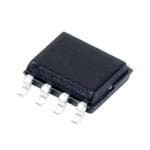
| 产品图片 |
|
| rohs | 符合RoHS无铅 / 符合限制有害物质指令(RoHS)规范要求 |
| 产品系列 | 电源管理 IC,稳压器—开关式稳压器,Texas Instruments TPS5431DDASWIFT™ |
| 数据手册 | |
| 产品型号 | TPS5431DDA |
| PWM类型 | 电压模式 |
| 产品培训模块 | http://www.digikey.cn/PTM/IndividualPTM.page?site=cn&lang=zhs&ptm=16804 |
| 产品目录页面 | |
| 产品种类 | 稳压器—开关式稳压器 |
| 供应商器件封装 | 8-SO PowerPad |
| 其它名称 | 296-19662-5 |
| 制造商产品页 | http://www.ti.com/general/docs/suppproductinfo.tsp?distId=10&orderablePartNumber=TPS5431DDA |
| 包装 | 管件 |
| 单位重量 | 70.600 mg |
| 同步整流器 | 无 |
| 商标 | Texas Instruments |
| 安装类型 | 表面贴装 |
| 安装风格 | SMD/SMT |
| 宽度 | 3.9 mm |
| 封装 | Tube |
| 封装/外壳 | 8-SOIC(0.154",3.90mm 宽)裸焊盘 |
| 封装/箱体 | HSOP-8 |
| 工作温度 | -40°C ~ 125°C |
| 工作温度范围 | - 40 C to + 125 C |
| 工厂包装数量 | 75 |
| 开关频率 | 500 kHz |
| 拓扑结构 | Buck |
| 最大工作温度 | + 125 C |
| 最大输入电压 | 23 V |
| 最小工作温度 | - 40 C |
| 最小输入电压 | 5.5 V |
| 标准包装 | 75 |
| 电压-输入 | 5.5 V ~ 23 V |
| 电压-输出 | 1.23 V ~ 20 V |
| 电流-输出 | 3A |
| 类型 | 降压(降压) |
| 系列 | TPS5431 |
| 输出数 | 1 |
| 输出电压 | 20 V |
| 输出电流 | 3 A |
| 输出端数量 | 1 Output |
| 输出类型 | 可调式 |
| 配用 | /product-detail/zh/TPS5431EVM-173/296-19710-ND/1045107 |
| 频率-开关 | 500kHz |


- 商务部:美国ITC正式对集成电路等产品启动337调查
- 曝三星4nm工艺存在良率问题 高通将骁龙8 Gen1或转产台积电
- 太阳诱电将投资9.5亿元在常州建新厂生产MLCC 预计2023年完工
- 英特尔发布欧洲新工厂建设计划 深化IDM 2.0 战略
- 台积电先进制程称霸业界 有大客户加持明年业绩稳了
- 达到5530亿美元!SIA预计今年全球半导体销售额将创下新高
- 英特尔拟将自动驾驶子公司Mobileye上市 估值或超500亿美元
- 三星加码芯片和SET,合并消费电子和移动部门,撤换高东真等 CEO
- 三星电子宣布重大人事变动 还合并消费电子和移动部门
- 海关总署:前11个月进口集成电路产品价值2.52万亿元 增长14.8%


PDF Datasheet 数据手册内容提取
Product Order Technical Tools & Support & Reference Folder Now Documents Software Community Design TPS5430,TPS5431 SLVS632I–JANUARY2006–REVISEDAPRIL2017 TPS543x 3-A, Wide Input Range, Step-Down Converter 1 Features 3 Description • WideInputVoltageRange: TheTPS543xisahigh-output-currentPWMconverter 1 that integrates a low-resistance, high-side N-channel – TPS5430:5.5Vto36V MOSFET. Included on the substrate with the listed – TPS5431:5.5Vto23V features are a high-performance voltage error • Upto3-AContinuous(4-APeak)OutputCurrent amplifier that provides tight voltage regulation accuracy under transient conditions; an undervoltage- • HighEfficiencyupto95%Enabledby110-mΩ lockout circuit to prevent start-up until the input IntegratedMOSFETSwitch voltage reaches 5.5 V; an internally set slow-start • WideOutputVoltageRange:AdjustableDownto circuit to limit inrush currents; and a voltage feed- 1.22Vwith1.5%InitialAccuracy forward circuit to improve the transient response. • InternalCompensationMinimizesExternalParts Using the ENA pin, shutdown supply current is reduced to 18 μA typically. Other features include an Count active-high enable, overcurrent limiting, over-voltage • Fixed500kHzSwitchingFrequencyforSmall protection and thermal shutdown. To reduce design FilterSize complexity and external component count, the • ImprovedLineRegulationandTransient TPS543x feedback loop is internally compensated. ResponsebyInputVoltageFeedForward The TPS5431 is intended to operate from power rails up to 23 V. The TPS5430 regulates a wide variety of • SystemProtectedbyOvercurrentLimiting, powersourcesincluding24Vbus. OvervoltageProtectionandThermalShutdown • –40°Cto125°COperatingJunctionTemperature The TPS543x device is available in a thermally enhanced, easy to use 8-pin SOIC PowerPAD™ Range package. TI provides evaluation modules and the • AvailableinSmallThermallyEnhanced8-PinSO Designer software tool to aid in quickly achieving PowerPAD™Package high-performance power supply designs to meet • CreateaCustomDesignUsingtheTPS5430With aggressiveequipmentdevelopmentcycles. theWEBENCH®PowerDesigner DeviceInformation(1) 2 Applications PARTNUMBER PACKAGE INPUTVOLTAGE • Consumer:Set-topBox,DVD,LCDDisplays TPS5430 5.5Vto36V HSOP(8) TPS5431 5.5Vto23V • IndustrialandCarAudioPowerSupplies • BatteryChargers,HighPowerLEDSupply (1) For all available packages, see the orderable addendum at theendofthedatasheet. • 12-V/24-VDistributedPowerSystems Simplified Schematic Efficiency vs Output Current 100 VIN VOUT VIN PH 95 TPS5430/31 90 NC BOOT % 85 − 80 NC cy en 75 ci ENA VSENSE Effi 70 GND 65 VI= 12 V V = 5 V O 60 f = 500 kHz s 55 TA= 25oC 50 0 0.5 1 1.5 2 2.5 3 3.5 IO-Output Current-A 1 An IMPORTANT NOTICE at the end of this data sheet addresses availability, warranty, changes, use in safety-critical applications, intellectualpropertymattersandotherimportantdisclaimers.PRODUCTIONDATA.
TPS5430,TPS5431 SLVS632I–JANUARY2006–REVISEDAPRIL2017 www.ti.com Table of Contents 1 Features.................................................................. 1 7.4 DeviceFunctionalModes........................................12 2 Applications........................................................... 1 8 ApplicationandImplementation........................ 13 3 Description............................................................. 1 8.1 ApplicationInformation............................................13 4 RevisionHistory..................................................... 2 8.2 TypicalApplications................................................14 5 PinConfigurationandFunctions......................... 4 9 PowerSupplyRecommendations...................... 26 6 Specifications......................................................... 5 10 Layout................................................................... 26 6.1 AbsoluteMaximumRatings......................................5 10.1 LayoutGuidelines.................................................26 6.2 ESDRatings..............................................................5 10.2 LayoutExample....................................................27 6.3 RecommendedOperatingConditions.......................5 11 DeviceandDocumentationSupport................. 28 6.4 ThermalInformation..................................................6 11.1 DeviceSupport......................................................28 6.5 ElectricalCharacteristics...........................................7 11.2 RelatedLinks........................................................28 6.6 TypicalCharacteristics..............................................8 11.3 Trademarks...........................................................28 7 DetailedDescription............................................ 10 11.4 ElectrostaticDischargeCaution............................28 7.1 Overview.................................................................10 11.5 Glossary................................................................28 7.2 FunctionalBlockDiagram.......................................10 12 Mechanical,Packaging,andOrderable Information........................................................... 28 7.3 FeatureDescription.................................................11 4 Revision History ChangesfromRevisionH(April2016)toRevisionI Page • AddedWEBENCH®Model ................................................................................................................................................... 1 • ChangedAbsoluteMaximumRatingsPH(transient<10ns)specMINvoltagefrom"–1.2"to"–4".................................... 5 ChangesfromRevisionG(February2015)toRevisionH Page • Deleted"RecommendedLandPattern"figurefromcoredatasheet.NewdrawingsarefurnishedintheMechanical, Packaging,andOrderableInformationsection.................................................................................................................... 27 ChangesfromRevisionF(December2014)toRevisionG Page • FixedtypoerrorTPS5430xtoTPS513x................................................................................................................................ 1 ChangesfromRevisionE(September2013)toRevisionF Page • AddedESDRatingtable,FeatureDescriptionsection,DeviceFunctionalModes,ApplicationandImplementation section,PowerSupplyRecommendationssection,Layoutsection,DeviceandDocumentationSupportsection,and Mechanical,Packaging,andOrderableInformationsection ................................................................................................. 4 ChangesfromRevisionD(January2013)toRevisionE Page • DeletedSWIFTfromthedatasheetTitle,Features,andDescription.................................................................................... 1 ChangesfromRevisionC(November2006)toRevisionD Page • ReplacedtheDISSIPATIONRATINGSwiththeTHERMALINFORMATIONtable............................................................... 5 2 SubmitDocumentationFeedback Copyright©2006–2017,TexasInstrumentsIncorporated ProductFolderLinks:TPS5430 TPS5431
TPS5430,TPS5431 www.ti.com SLVS632I–JANUARY2006–REVISEDAPRIL2017 ChangesfromRevisionB(August2006)toRevisionC Page • ChangedtheEfficiencyvsOutputCurrentgraph................................................................................................................... 1 • ChangedtheFUNCTIONALBLOCKDIAGRAM.................................................................................................................. 10 • AddedtheCircuitUsingCeramicOutputFilterCapacitorssection...................................................................................... 24 ChangesfromRevisionA(March2006)toRevisionB Page • AddedNote3totheABSOLUTEMAXIMUMRATINGStable............................................................................................... 4 ChangesfromOriginal(January2006)toRevisionA Page • AddedAddeddevicenumberTPS5431................................................................................................................................. 1 • ChangedFigure17............................................................................................................................................................... 22 • AddedFigure18................................................................................................................................................................... 23 Copyright©2006–2017,TexasInstrumentsIncorporated SubmitDocumentationFeedback 3 ProductFolderLinks:TPS5430 TPS5431
TPS5430,TPS5431 SLVS632I–JANUARY2006–REVISEDAPRIL2017 www.ti.com 5 Pin Configuration and Functions DDAPackage 8-PinSOICwithThermalPad TopView BOOT 1 8 PH NC 2 7 VIN PowerPAD NC 3 6 GND VSENSE 4 5 ENA PinFunctions PIN I/O DESCRIPTION NAME NO. Boostcapacitorforthehigh-sideFETgatedriver.Connect0.01μFlowESRcapacitorfromBOOTpintoPH BOOT 1 O pin. NC 2,3 — Notconnectedinternally. VSENSE 4 I Feedbackvoltagefortheregulator.Connecttooutputvoltagedivider. ENA 5 I On/offcontrol.Below0.5V,thedevicestopsswitching.Floatthepintoenable. GND 6 — Ground.ConnecttoPowerPAD. Inputsupplyvoltage.BypassVINpintoGNDpinclosetodevicepackagewithahighquality,lowESR VIN 7 — ceramiccapacitor. PH 8 I SourceofthehighsidepowerMOSFET.Connectedtoexternalinductoranddiode. PowerPAD — GNDpinmustbeconnectedtotheexposedpadforproperoperation. 4 SubmitDocumentationFeedback Copyright©2006–2017,TexasInstrumentsIncorporated ProductFolderLinks:TPS5430 TPS5431
TPS5430,TPS5431 www.ti.com SLVS632I–JANUARY2006–REVISEDAPRIL2017 6 Specifications 6.1 Absolute Maximum Ratings overoperatingfree-airtemperaturerange(unlessotherwisenoted) (1)(2) MIN MAX UNIT VIN –0.3 40(3) TPS5430 PH(steady-state) –0.6 40(3) V Inputvoltagerange I VIN –0.3 25 TPS5431 PH(steady-state) –0.6 25 ENA –0.3 7 BOOT-PH –0.3 10 V VSENSE –0.3 3 PH(transient<10ns) –4 I Sourcecurrent PH Internally O Limited I Leakagecurrent PH 10 μA lkg T Operatingvirtualjunctiontemperaturerange –40 150 °C J T Storagetemperaturerange –65 150 °C stg (1) StressesbeyondthoselistedunderAbsoluteMaximumRatingsmaycausepermanentdamagetothedevice.Thesearestressratings onlyandfunctionaloperationofthedeviceattheseoranyotherconditionsbeyondthoseindicatedunderRecommendedOperating Conditionsisnotimplied.Exposuretoabsolute-maximum-ratedconditionsforextendedperiodsmayaffectdevicereliability. (2) Allvoltagevaluesarewithrespecttonetworkgroundterminal. (3) ApproachingtheabsolutemaximumratingfortheVINpinmaycausethevoltageonthePHpintoexceedtheabsolutemaximumrating. 6.2 ESD Ratings VALUE UNIT Human-bodymodel(HBM),perANSI/ESDA/JEDECJS-001(1) ±2000 V(ESD) Electrostaticdischarge Charged-devicemodel(CDM),perJEDECspecificationJESD22- ±1500 V C101(2) (1) JEDECdocumentJEP155statesthat500-VHBMallowssafemanufacturingwithastandardESDcontrolprocess. (2) JEDECdocumentJEP157statesthat250-VCDMallowssafemanufacturingwithastandardESDcontrolprocess. 6.3 Recommended Operating Conditions MIN MAX UNIT TPS5430 5.5 36 VIN Inputvoltagerange V TPS5431 5.5 23 T Operatingjunctiontemperature –40 125 °C J Copyright©2006–2017,TexasInstrumentsIncorporated SubmitDocumentationFeedback 5 ProductFolderLinks:TPS5430 TPS5431
TPS5430,TPS5431 SLVS632I–JANUARY2006–REVISEDAPRIL2017 www.ti.com 6.4 Thermal Information TPS5430 TPS5431 THERMALMETRIC(1)(2)(3) UNIT DDA 8PINS R Junction-to-ambientthermalresistance(2-layercustomboard) (4) 33 θJA R Junction-to-ambientthermalresistance(4-layercustomboard) (5) 26 θJA R Junction-to-ambientthermalresistance(standardboard) 42.3 θJA ψ Junction-to-topcharacterizationparameter 4.9 JT °C/W ψ Junction-to-boardcharacterizationparameter 20.7 JB R Junction-to-case(top)thermalresistance 46.4 θJC(top) R Junction-to-case(bottom)thermalresistance 0.8 θJC(bottom) R Junction-to-boardthermalresistance 20.8 θJB (1) Formoreinformationabouttraditionalandnewthermalmetrics,seetheICPackageThermalMetricsapplicationreport,SPRA953. (2) Maximumpowerdissipationmaybelimitedbyovercurrentprotection (3) PowerratingataspecificambienttemperatureT shouldbedeterminedwithajunctiontemperatureof125°C.Thisisthepointwhere A distortionstartstosubstantiallyincrease.ThermalmanagementofthefinalPCBshouldstrivetokeepthejunctiontemperatureator below125°Cforbestperformanceandlong-termreliability.SeeThermalCalculationsinapplicationssectionofthisdatasheetformore information. (4) Testboardsconditions: (a)3inx3in,2layers,thickness:0.062inch. (b)2oz.coppertraceslocatedonthetopandbottomofthePCB. (c)6thermalviasinthePowerPADareaunderthedevicepackage. (5) Testboardconditions: (a) 3inx3in,4layers,thickness:0.062inch. (b)2oz.coppertraceslocatedonthetopandbottomofthePCB. (c)2oz.coppergroundplanesonthe2internallayers. (d)6thermalviasinthePowerPADareaunderthedevicepackage. 6 SubmitDocumentationFeedback Copyright©2006–2017,TexasInstrumentsIncorporated ProductFolderLinks:TPS5430 TPS5431
TPS5430,TPS5431 www.ti.com SLVS632I–JANUARY2006–REVISEDAPRIL2017 6.5 Electrical Characteristics T =–40°Cto125°C,VIN=12V(unlessotherwisenoted) J PARAMETER TESTCONDITIONS MIN TYP MAX UNIT SUPPLYVOLTAGE(VINPIN) VSENSE=2V,Notswitching, 3 4.4 mA I Quiescentcurrent PHpinopen Q Shutdown,ENA=0V 18 50 μA UNDERVOLTAGELOCKOUT(UVLO) Startthresholdvoltage,UVLO 5.3 5.5 V Hysteresisvoltage,UVLO 330 mV VOLTAGEREFERENCE T =25°C 1.202 1.221 1.239 J Voltagereferenceaccuracy V I =0A–3A 1.196 1.221 1.245 O OSCILLATOR Internallysetfree-runningfrequency 400 500 600 kHz Minimumcontrollableontime 150 200 ns Maximumdutycycle 87% 89% ENABLE(ENAPIN) Startthresholdvoltage,ENA 1.3 V Stopthresholdvoltage,ENA 0.5 V Hysteresisvoltage,ENA 450 mV Internalslow-starttime(0~100%) 6.6 8 10 ms CURRENTLIMIT Currentlimit 4 5 6 A Currentlimithiccuptime 13 16 20 ms THERMALSHUTDOWN Thermalshutdowntrippoint 135 162 °C Thermalshutdownhysteresis 14 OUTPUTMOSFET VIN=5.5V 150 r High-sidepowerMOSFETswitch mΩ DS(on) 110 230 Copyright©2006–2017,TexasInstrumentsIncorporated SubmitDocumentationFeedback 7 ProductFolderLinks:TPS5430 TPS5431
TPS5430,TPS5431 SLVS632I–JANUARY2006–REVISEDAPRIL2017 www.ti.com 6.6 Typical Characteristics 530 3.5 VI= 12 V 520 f−Oscillator Frequency−kHz 445589010000 I−Quiescen−mAt CurrentQ 23..72355 470 460 2.5 −50 −25 0 25 50 75 100 125 −50 −25 0 25 50 75 100 125 T −Junction Temperature−°C TJ−Junction Temperature−°C Figure1.OscillatorFrequencyvs.JunctionTemperature Figure2.Non-SwitchingQuiescentCurrentvs.Junction Temperature 25 1.230 ENA = 0 V −µA 20 TJ= 125°C e - V 1.225 c −Shutdown CurrentSD 1105 TJTJ==– 2470°°CC V- Voltage ReferenREF 11..221250 I 5 1.210 0 5 10 15 20 25 30 35 40 -50 -25 0 25 50 75 100 125 VI−Input Voltage−V TJ- Junction Temperature - °C Figure3.ShutdownQuiescentCurrentvs.InputVoltage Figure4.VoltageReferencevs.JunctionTemperature 180 9 VI= 12 V 170 ms mΩ− 160 me− 8.5 150 iT Resistance 113400 Slow Start 8 r−On DS(on) 111102000 T−Internal SS 7.5 90 7 80 −50 −25 0 25 50 75 100 125 −50 −25 0 25 50 75 100 125 TJ−Junction Temperature− °C TJ−Junction Temperature −°C Figure5.OnResistancevs.JunctionTemperature Figure6.InternalSlowStartTimevs.JunctionTemperature 8 SubmitDocumentationFeedback Copyright©2006–2017,TexasInstrumentsIncorporated ProductFolderLinks:TPS5430 TPS5431
TPS5430,TPS5431 www.ti.com SLVS632I–JANUARY2006–REVISEDAPRIL2017 Typical Characteristics (continued) 180 8 ns 170 − e 7.75 imntrollable On T 115600 m Duty Ratio - % 7.50 o u C m m 140 ni u Mi 7.25 m ni Mi 130 7 -50 -25 0 25 50 75 100 125 120−50 −25 0 25 50 75 100 125 TJ- Junction Temperature - °C TJ−Junction Temperature− °C Figure7.MinimumControllableOnTimevs.Junction Figure8.MinimumControllableDutyRatiovs.Junction Temperature Temperature Copyright©2006–2017,TexasInstrumentsIncorporated SubmitDocumentationFeedback 9 ProductFolderLinks:TPS5430 TPS5431
TPS5430,TPS5431 SLVS632I–JANUARY2006–REVISEDAPRIL2017 www.ti.com 7 Detailed Description 7.1 Overview The TPS543x is a 3-A, step-down (buck) regulator with an integrated high-side n-channel MOSFET. The TPS5431 is intended to operate from power rails up to 23 V and the TPS5430 up to 36 V. These devices implement constant-frequency voltage-mode control with voltage feed forward for improved line regulation and linetransientresponse.Internalcompensationreducesdesigncomplexityandexternalcomponentcount. The integrated 110-mΩ high-side MOSFET supports high-efficiency power-supply designs capable of delivering 3-A of continuous current to a load. The gate-drive bias voltage for the integrated high-side MOSFET is supplied by a bootstrap capacitor connected from the BOOT to PH pins. The TPS543x reduces the external component countbyintegratingthebootstraprechargediode. The TPS543x has a default input start-up voltage of 5.3 V typical. The ENA pin can be used to disable the TPS543x reducing the supply current to 18 µA. An internal pullup current source enables operation when the ENApinisfloating.TheTPS543xincludesaninternalslow-startcircuitthatslowstheoutputrisetimeduringstart up to reduce in rush current and output voltage overshoot. The minimum output voltage is the internal 1.221-V feedback reference. Output overvoltage transients are minimized by an Overvoltage Protection (OVP) comparator. When the OVP comparator is activated, the high-side MOSFET is turned off and remains off until theoutputvoltageislessthan112.5%ofthedesiredoutputvoltage. Internal cycle-by-cycle overcurrent protection limits the peak current in the integrated high-side MOSFET. For continuous overcurrent fault conditions the TPS543x will enter hiccup mode overcurrent limiting. Thermal protectionprotectsthedevicefromoverheating. 7.2 Functional Block Diagram VIN VIN UVLO 1.22R1e Vfe Breanncdegap VREF Slow Start SHDN ReBgouolattor BOOT HICCUP 5µA ENA ENABLE SHDN SHDN VSENSE Z1 Thermal Protection SHDN SHDN AmErprolifrier Z2 Ramp NC VIN Generator Feed Forward Gain = 25 NC SHDN PWM HICCUP Comparator GND Overcurrent SHDN Oscillator Protection SHDN Gate Drive VSENSE OVP Control POWERPAD 112.5% VREF Gate Driver SHDN BOOT PH VOUT Copyright ©Texas Instruments Incorporated 10 SubmitDocumentationFeedback Copyright©2006–2017,TexasInstrumentsIncorporated ProductFolderLinks:TPS5430 TPS5431
TPS5430,TPS5431 www.ti.com SLVS632I–JANUARY2006–REVISEDAPRIL2017 7.3 Feature Description 7.3.1 OscillatorFrequency The internal free running oscillator sets the PWM switching frequency at 500 kHz. The 500 kHz switching frequency allows less output inductance for the same output ripple requirement resulting in a smaller output inductor. 7.3.2 VoltageReference The voltage reference system produces a precision reference signal by scaling the output of a temperature stable bandgap circuit. The bandgap and scaling circuits are trimmed during production testing to an output of 1.221Vatroomtemperature. 7.3.3 Enable(ENA)andInternalSlowStart The ENA pin provides electrical on/off control of the regulator. Once the ENA pin voltage exceeds the threshold voltage, the regulator starts operation and the internal slow start begins to ramp. If the ENA pin voltage is pulled below the threshold voltage, the regulator stops switching and the internal slow start resets. Connecting the pin to ground or to any voltage less than 0.5 V will disable the regulator and activate the shutdown mode. The quiescentcurrentoftheTPS543xinshutdownmodeistypically18 μA. The ENA pin has an internal pull-up current source, allowing the user to float the ENA pin. If an application requires controlling the ENA pin, use open drain or open collector output logic to interface with the pin. To limit the start-up inrush current, an internal slow-start circuit is used to ramp up the reference voltage from 0 V to its finalvalue,linearly.Theinternalslowstarttimeis8mstypically. 7.3.4 UndervoltageLockout(UVLO) The TPS543x incorporate an undervoltage lockout circuit to keep the device disabled when VIN (the input voltage) is below the UVLO start voltage threshold. During power up, internal circuits are held inactive and the internal slow start is grounded until VIN exceeds the UVLO start threshold voltage. Once the UVLO start threshold voltage is reached, the internal slow start is released and device start-up begins. The device operates untilVINfallsbelowtheUVLOstopthresholdvoltage.ThetypicalhysteresisintheUVLOcomparatoris330 mV. 7.3.5 BoostCapacitor(BOOT) Connect a 0.01 μF low-ESR ceramic capacitor between the BOOT pin and PH pin. This capacitor provides the gate drive voltage for the high-side MOSFET. X7R or X5R grade dielectrics are recommended due to their stable valuesovertemperature. 7.3.6 OutputFeedback(VSENSE)andInternalCompensation The output voltage of the regulator is set by feeding back the center point voltage of an external resistor divider network to the VSENSE pin. In steady-state operation, the VSENSE pin voltage should be equal to the voltage reference1.221V. The TPS543x implements internal compensation to simplify the regulator design. Since the TPS543x uses voltage mode control, a type 3 compensation network has been designed on chip to provide a high crossover frequency and a high phase margin for good stability. See the Internal Compensation Network in the applications sectionformoredetails. 7.3.7 VoltageFeed-Forward The internal voltage feed-forward provides a constant dc power stage gain despite any variations with the input voltage. This greatly simplifies the stability analysis and improves the transient response. Voltage feed forward varies the peak ramp voltage inversely with the input voltage so that the modulator and power stage gain are constantatthefeedforwardgain,i.e. FeedForwardGain(cid:2) VIN Ramp pk(cid:1)pk (1) ThetypicalfeedforwardgainofTPS543xis25. Copyright©2006–2017,TexasInstrumentsIncorporated SubmitDocumentationFeedback 11 ProductFolderLinks:TPS5430 TPS5431
TPS5430,TPS5431 SLVS632I–JANUARY2006–REVISEDAPRIL2017 www.ti.com Feature Description (continued) 7.3.8 Pulse-Width-Modulation(PWM)Control The regulator employs a fixed frequency pulse-width-modulator (PWM) control method. First, the feedback voltage (VSENSE pin voltage) is compared to the constant voltage reference by the high gain error amplifier and compensationnetworktoproduceaerrorvoltage.Then,theerrorvoltageiscomparedtotherampvoltagebythe PWM comparator. In this way, the error voltage magnitude is converted to a pulse width which is the duty cycle. Finally,thePWMoutputisfedintothegatedrivecircuittocontroltheon-timeofthehigh-sideMOSFET. 7.3.9 OvercurrentLimiting Overcurrent limiting is implemented by sensing the drain-to-source voltage across the high-side MOSFET. The drain to source voltage is then compared to a voltage level representing the overcurrent threshold limit. If the drain-to-source voltage exceeds the overcurrent threshold limit, the overcurrent indicator is set true. The system willignoretheovercurrentindicatorfortheleadingedgeblankingtimeatthebeginningofeachcycletoavoidany turn-onnoiseglitches. Once overcurrent indicator is set true, overcurrent limiting is triggered. The high-side MOSFET is turned off for the rest of the cycle after a propagation delay. The overcurrent limiting mode is called cycle-by-cycle current limiting. Sometimes under serious overload conditions such as short-circuit, the overcurrent runaway may still happen when using cycle-by-cycle current limiting. A second mode of current limiting is used, i.e. hiccup mode overcurrentlimiting.Duringhiccupmodeovercurrentlimiting,thevoltagereferenceisgroundedandthehigh-side MOSFETisturnedoffforthehiccuptime.Oncethehiccuptimedurationiscomplete,theregulatorrestartsunder controloftheslowstartcircuit. 7.3.10 OvervoltageProtection The TPS543x has an overvoltage protection (OVP) circuit to minimize voltage overshoot when recovering from output fault conditions. The OVP circuit includes an overvoltage comparator to compare the VSENSE pin voltage and a threshold of 112.5% x VREF. Once the VSENSE pin voltage is higher than the threshold, the high-side MOSFET will be forced off. When the VSENSE pin voltage drops lower than the threshold, the high-side MOSFETwillbeenabledagain. 7.3.11 ThermalShutdown The TPS543x protects itself from overheating with an internal thermal shutdown circuit. If the junction temperature exceeds the thermal shutdown trip point, the voltage reference is grounded and the high-side MOSFET is turned off. The part is restarted under control of the slow start circuit automatically when the junction temperaturedrops14°Cbelowthethermalshutdowntrippoint. 7.4 Device Functional Modes 7.4.1 OperationnearMinimumInputVoltage The TPS543x is recommended to operate with input voltages above 5.5 V. The typical VIN UVLO threshold is 5.3VandthedevicemayoperateatinputvoltagesdowntotheUVLOvoltage.Atinputvoltagesbelowtheactual UVLO voltage the device will not switch. If EN is floating or externally pulled up to greater up than 1.3 V, when V passes the UVLO threshold the TPS543x will become active. Switching is enabled and the slow-start (VIN) sequence is initiated. The TPS543x starts linearly ramping up the internal reference voltage from 0 V to its final valueovertheinternalslow-starttimeperiod. 7.4.2 OperationwithENAcontrol The enable start threshold voltage is 1.3 V max. With ENA held below the 0.5 V minimum stop threshold voltage the TPS543x is disabled and switching is inhibited even if VIN is above its UVLO threshold. The quiescent current is reduced in this state. If the ENA voltage is increased above the max start threshold while V is (VIN) above the UVLO threshold, the device becomes active. Switching is enabled and the slow-start sequence is initiated.TheTPS543xstartslinearlyrampinguptheinternalreferencevoltagefrom0Vtoitsfinalvalueoverthe internalslow-starttimeperiod. 12 SubmitDocumentationFeedback Copyright©2006–2017,TexasInstrumentsIncorporated ProductFolderLinks:TPS5430 TPS5431
TPS5430,TPS5431 www.ti.com SLVS632I–JANUARY2006–REVISEDAPRIL2017 8 Application and Implementation NOTE Information in the following applications sections is not part of the TI component specification, and TI does not warrant its accuracy or completeness. TI’s customers are responsible for determining suitability of components for their purposes. Customers should validateandtesttheirdesignimplementationtoconfirmsystemfunctionality. 8.1 Application Information The TPS543x is a 3-A, step down regulator with an integrated high side MOSFET. This device is typically used to convert a higher DC voltage to a lower DC voltage with a maximum available output current of 3 A. Example applications are: High Density Point-of-Load Regulators for Set-top Box, DVD, LCD and Plasma Displays, High Power LED Supply, Car Audio, Battery Chargers, and other 12-V and 24-V Distributed Power Systems. Use the following design procedure to select component values for the TPS543x. This procedure illustrates the design of a high frequency switching regulator. Alternatively, use the WEBENCH software to generate a complete design. The WEBENCH software uses an iterative design procedure and accesses a comprehensive database of componentswhengeneratingadesign. Tobeginthedesignprocessafewparametersmustbedecidedupon.Thedesignerneedstoknowthefollowing: • Inputvoltagerange • Outputvoltage • Inputripplevoltage • Outputripplevoltage • Outputcurrentrating • Operatingfrequency Copyright©2006–2017,TexasInstrumentsIncorporated SubmitDocumentationFeedback 13 ProductFolderLinks:TPS5430 TPS5431
TPS5430,TPS5431 SLVS632I–JANUARY2006–REVISEDAPRIL2017 www.ti.com 8.2 Typical Applications 8.2.1 12-VInputto5.0-VOutput Figure 9 shows the schematic for a typical TPS5430 application. The TPS5430 can provide up to 3 A output current at a nominal output voltage of 5 V. For proper thermal performance, the exposed PowerPAD™ underneaththedevicemustbesoldereddowntotheprinted-circuitboard. U1 TPS5430DDA C2 L1 10.8 - 19.8 V 7 0.01mF 15mH VIN VIN 1 5 V 5 BOOT VOUT EN ENA C101mF 23 NNCC PH 48 DB3140A + C2230mF R101 kW 6 VSNS GND PwPd 9 R2 3.24 kW Copyright ©Texas Instruments Incorporated Figure9. ApplicationCircuit,12VInputto5.0VOutput 8.2.1.1 DesignRequirements Forthisdesignexample,usethefollowingastheinputparameters: DESIGNPARAMETER(1) EXAMPLEVALUE Inputvoltagerange 10.8Vto19.8V Outputvoltage 5V Inputripplevoltage 300mV Outputripplevoltage 30mV Outputcurrentrating 3A Operatingfrequency 500kHz (1) Asanadditionalconstraint,thedesignissetuptobesmallsizeandlowcomponentheight. 14 SubmitDocumentationFeedback Copyright©2006–2017,TexasInstrumentsIncorporated ProductFolderLinks:TPS5430 TPS5431
TPS5430,TPS5431 www.ti.com SLVS632I–JANUARY2006–REVISEDAPRIL2017 8.2.1.2 DetailedDesignProcedure The following design procedure can be used to select component values for the TPS5430. This section presents asimplifieddiscussionofthedesignprocess. 8.2.1.2.1 CustomDesignWithWEBENCH®Tools ClickheretocreateacustomdesignusingtheTPS5430devicewiththeWEBENCH® PowerDesigner. 1. Startbyenteringtheinputvoltage(V ),outputvoltage(V ),andoutputcurrent(I )requirements. IN OUT OUT 2. Optimizethedesignforkeyparameterssuchasefficiency,footprint,andcostusingtheoptimizerdial. 3. ComparethegenerateddesignwithotherpossiblesolutionsfromTexasInstruments. The WEBENCH Power Designer provides a customized schematic along with a list of materials with real-time pricingandcomponentavailability. Inmostcases,theseactionsareavailable: • Runelectricalsimulationstoseeimportantwaveformsandcircuitperformance • Runthermalsimulationstounderstandboardthermalperformance • ExportcustomizedschematicandlayoutintopopularCADformats • PrintPDFreportsforthedesign,andsharethedesignwithcolleagues GetmoreinformationaboutWEBENCHtoolsatwww.ti.com/WEBENCH. 8.2.1.2.2 SwitchingFrequency The switching frequency for the TPS5430 is internally set to 500 kHz. It is not possible to adjust the switching frequency. 8.2.1.2.3 InputCapacitors The TPS5430 requires an input decoupling capacitor and, depending on the application, a bulk input capacitor. The recommended value for the decoupling capacitor, C1, is 10 μF. A high quality ceramic type X5R or X7R is required. For some applications, a smaller value decoupling capacitor may be used, so long as the input voltage and current ripple ratings are not exceeded. The voltage rating must be greater than the maximum input voltage, includingripple. ThisinputripplevoltagecanbeapproximatedbyEquation2: (cid:1)VIN(cid:3)IOCUBTU(MLAKX(cid:1))(cid:1)ƒs0w.25(cid:2)(cid:4)IOUT(MAX)(cid:1)ESRMAX(cid:5) (2) Where I is the maximum load current, f is the switching frequency, C is the input capacitor value and OUT(MAX) SW IN ESR isthemaximumseriesresistanceoftheinputcapacitor. MAX The maximum RMS ripple current also needs to be checked. For worst case conditions, this can be approximatedbyEquation3: I OUT(MAX) I (cid:1) CIN 2 (3) In this case the input ripple voltage would be 156 mV and the RMS ripple current would be 1.5 A. The maximum voltage across the input capacitors would be V max plus delta V /2. The chosen input decoupling capacitor is IN IN ratedfor25Vandtheripplecurrentcapacityisgreaterthan3A,providingamplemargin.Itisveryimportantthat themaximumratingsforvoltageandcurrentarenotexceededunderanycircumstance. Additionally some bulk capacitance may be needed, especially if the TPS5430 circuit is not located within about 2 inches from the input voltage source. The value for this capacitor is not critical but it also should be rated to handle the maximum input voltage including ripple voltage and should filter the output so that input ripple voltage isacceptable. Copyright©2006–2017,TexasInstrumentsIncorporated SubmitDocumentationFeedback 15 ProductFolderLinks:TPS5430 TPS5431
TPS5430,TPS5431 SLVS632I–JANUARY2006–REVISEDAPRIL2017 www.ti.com 8.2.1.2.4 OutputFilterComponents Two components need to be selected for the output filter, L1 and C2. Since the TPS5430 is an internally compensateddevice,alimitedrangeoffiltercomponenttypesandvaluescanbesupported. 8.2.1.2.4.1 InductorSelection Tocalculatetheminimumvalueoftheoutputinductor,useEquation4: (cid:4) (cid:5) VOUT(MAX)(cid:1) VIN(MAX)(cid:2) VOUT LMIN(cid:3) VIN(max)(cid:1)KIND(cid:1)IOUT(cid:1)FSW (4) K is a coefficient that represents the amount of inductor ripple current relative to the maximum output current. IND Three things need to be considered when determining the amount of ripple current in the inductor: the peak to peak ripple current affects the output ripple voltage amplitude, the ripple current affects the peak switch current and the amount of ripple current determines at what point the circuit becomes discontinuous. For designs using the TPS5430, K of 0.2 to 0.3 yields good results. Low output ripple voltages can be obtained when paired with IND theproperoutputcapacitor,thepeakswitchcurrentwillbewellbelowthecurrentlimitsetpointandrelativelylow loadcurrentscanbesourcedbeforediscontinuousoperation. For this design example use K = 0.2 and the minimum inductor value is calculated to be 12.5 μH. The next IND higheststandardvalueis15μH,whichisusedinthisdesign. For the output filter inductor it is important that the RMS current and saturation current ratings not be exceeded. TheRMSinductorcurrentcanbefoundfromEquation5: (cid:7) 2 2 1 (cid:5) VOUT(cid:1)(cid:5)VIN(MAX)(cid:3)VOUT(cid:6) (cid:6) IL(RMS)(cid:4) IOUT(MAX)(cid:2)12(cid:1) VIN(MAX)(cid:1)LOUT(cid:1)FSW(cid:1)0.8 (5) andthepeakinductorcurrentcanbedeterminedwithEquation6: VOUT(cid:1)(cid:5)VIN(MAX)(cid:3)VOUT(cid:6) IL(PK)(cid:4)IOUT(MAX)(cid:2)1.6(cid:1)VIN(MAX)(cid:1)LOUT(cid:1)FSW (6) For this design, the RMS inductor current is 3.003 A, and the peak inductor current is 3.31 A. The chosen inductor is a Sumida CDRH104R-150 15 μH. It has a saturation current rating of 3.4 A and a RMS current rating of 3.6 A, easily meeting these requirements. A lesser rated inductor could be used, however this device was chosen because of its low profile component height. In general, inductor values for use with the TPS5430 are in therangeof10μHto100 μH. 16 SubmitDocumentationFeedback Copyright©2006–2017,TexasInstrumentsIncorporated ProductFolderLinks:TPS5430 TPS5431
TPS5430,TPS5431 www.ti.com SLVS632I–JANUARY2006–REVISEDAPRIL2017 8.2.1.2.4.2 CapacitorSelection The important design factors for the output capacitor are dc voltage rating, ripple current rating, and equivalent series resistance (ESR). The dc voltage and ripple current ratings cannot be exceeded. The ESR is important because along with the inductor ripple current it determines the amount of output ripple voltage. The actual value of the output capacitor is not critical, but some practical limits do exist. Consider the relationship between the desired closed loop crossover frequency of the design and LC corner frequency of the output filter. Due to the design of the internal compensation, it is desirable to keep the closed loop crossover frequency in the range 3 kHz to 30 kHz as this frequency range has adequate phase boost to allow for stable operation. For this design example, it is assumed that the intended closed loop crossover frequency will be between 2590 Hz and 24 kHz and also below the ESR zero of the output capacitor. Under these conditions the closed loop crossover frequencyisrelatedtotheLCcornerfrequencyby: f 2 f (cid:1) LC CO 85V OUT (7) Andthedesiredoutputcapacitorvaluefortheoutputfilterto: C (cid:2) 1 OUT 3357(cid:1)L (cid:1)f (cid:1)V OUT CO OUT (8) For a desired crossover of 18 kHz and a 15 μH inductor, the calculated value for the output capacitor is 220 μF. The capacitor type should be chosen so that the ESR zero is above the loop crossover. The maximum ESR shouldbe: ESR (cid:2) 1 MAX 2(cid:1)(cid:1)C (cid:1)f OUT CO (9) The maximum ESR of the output capacitor also determines the amount of output ripple as specified in the initial design parameters. The output ripple voltage is the inductor ripple current times the ESR of the output filter. Check that the maximum specified ESR as listed in the capacitor data sheet results in an acceptable output ripplevoltage: ( ) ESR x V x V - V MAX OUT IN(MAX) OUT V (MAX) = PP N x V x L x F C IN(MAX) OUT SW where • ΔV isthedesiredpeak-to-peakoutputripple. PP • N isthenumberofparalleloutputcapacitors. C • F istheswitchingfrequency. (10) SW For this design example, a single 220 μF output capacitor is chosen for C3. The calculated RMS ripple current is 143 mA and the maximum ESR required is 40 mΩ. A capacitor that meets these requirements is a Sanyo Poscap 10TPB220M, rated at 10 V with a maximum ESR of 40 mΩ and a ripple current rating of 3 A. An additionalsmall0.1μFceramicbypasscapacitormayalsoused,butisnotincludedinthisdesign. The minimum ESR of the output capacitor should also be considered. For good phase margin, the ESR zero when the ESR is at a minimum should not be too far above the internal compensation poles at 24 kHz and 54 kHz. The selected output capacitor must also be rated for a voltage greater than the desired output voltage plus one half the ripple voltage. Any derating amount must also be included. The maximum RMS ripple current in the outputcapacitorisgivenbyEquation11: (cid:7)VOUT(cid:1)(cid:4)VIN(MAX)(cid:2) VOUT(cid:5)(cid:9) 1 ICOUT(RMS)(cid:3)(cid:6)12(cid:1)(cid:11)(cid:8)VIN(MAX)(cid:1)LOUT(cid:1)FSW(cid:1)NC(cid:11)(cid:10) where • N isthenumberofoutputcapacitorsinparallel. C • F istheswitchingfrequency. (11) SW Copyright©2006–2017,TexasInstrumentsIncorporated SubmitDocumentationFeedback 17 ProductFolderLinks:TPS5430 TPS5431
TPS5430,TPS5431 SLVS632I–JANUARY2006–REVISEDAPRIL2017 www.ti.com OthercapacitortypescanbeusedwiththeTPS5430,dependingontheneedsoftheapplication. 8.2.1.2.5 OutputVoltageSet-Point The output voltage of the TPS5430 is set by a resistor divider (R1 and R2) from the output to the VSENSE pin. CalculatetheR2resistorvaluefortheoutputvoltageof5VusingEquation12: R2 (cid:3) R1(cid:1)1.221 V (cid:2) 1.221 OUT (12) ForanyTPS5430design,startwithanR1valueof10kΩ.R2isthen3.24kΩ. 8.2.1.2.6 BOOTCapacitor TheBOOTcapacitorshouldbe0.01μF. 8.2.1.2.7 CatchDiode The TPS5430 is designed to operate using an external catch diode between PH and GND. The selected diode must meet the absolute maximum ratings for the application: Reverse voltage must be higher than the maximum voltageatthePHpin,whichisV +0.5V.PeakcurrentmustbegreaterthanI plusonhalfthepeak IN(MAX) OUT(MAX) to peak inductor current. Forward voltage drop should be small for higher efficiencies. It is important to note that the catch diode conduction time is typically longer than the high-side FET on time, so attention paid to diode parameters can make a marked improvement in overall efficiency. Additionally, check that the device chosen is capable of dissipating the power losses. For this design, a Diodes, Inc. B340A is chosen, with a reverse voltage of40V,forwardcurrentof3A,andaforwardvoltagedropof0.5V. 8.2.1.2.8 AdvancedInformation 8.2.1.2.8.1 OutputVoltageLimitations Due to the internal design of the TPS543x, there are both upper and lower output voltage limits for any given input voltage. The upper limit of the output voltage set point is constrained by the maximum duty cycle of 87% andisgivenby: VOUTMAX(cid:4)0.87(cid:1)(cid:5)(cid:5)VINMIN(cid:3)IOMAX(cid:1)0.230(cid:6)(cid:2)VD(cid:6)(cid:3)(cid:5)IOMAX(cid:1)RL(cid:6)(cid:3)VD where • V =minimuminputvoltage INMIN • I =maximumloadcurrent OMAX • V =catchdiodeforwardvoltage. D • R =outputinductorseriesresistance. (13) L ThisequationassumesmaximumonresistancefortheinternalhighsideFET. The lower limit is constrained by the minimum controllable on time which may be as high as 200 ns. The approximateminimumoutputvoltageforagiveninputvoltageandminimumloadcurrentisgivenby: VOUTMIN(cid:4)0.12(cid:1)(cid:5)(cid:5)VINMAX(cid:3)IOMIN(cid:1)0.110(cid:6)(cid:2)VD(cid:6)(cid:3)(cid:5)IOMIN(cid:1)RL(cid:6)(cid:3)VD where • V =maximuminputvoltage INMAX • I =minimumloadcurrent OMIN • V =catchdiodeforwardvoltage. D • R =outputinductorseriesresistance. (14) L 8.2.1.2.8.2 InternalCompensationNetwork The design equations given in the example circuit can be used to generate circuits using the TPS543x. These designs are based on certain assumptions and will tend to always select output capacitors within a limited range ofESRvalues.Ifadifferentcapacitortypeisdesired,itmaybepossibletofitonetotheinternalcompensationof the TPS543x. Equation 15 gives the nominal frequency response of the internal voltage-mode type III compensationnetwork: 18 SubmitDocumentationFeedback Copyright©2006–2017,TexasInstrumentsIncorporated ProductFolderLinks:TPS5430 TPS5431
TPS5430,TPS5431 www.ti.com SLVS632I–JANUARY2006–REVISEDAPRIL2017 (cid:4)1(cid:2)2(cid:1)(cid:1)sFz1(cid:5)(cid:1)(cid:4)1(cid:2)2(cid:1)(cid:1)sFz2(cid:5) H(s)(cid:3) (cid:4) s (cid:5) (cid:4) s (cid:5) (cid:4) s (cid:5) (cid:4) s (cid:5) 2(cid:1)(cid:1)Fp0 (cid:1) 1(cid:2)2(cid:1)(cid:1)Fp1 (cid:1) 1(cid:2)2(cid:1)(cid:1)Fp2 (cid:1) 1(cid:2)2(cid:1)(cid:1)Fp3 where • fp0=2165Hz,fz1=2170Hz,fz2=2590Hz • fp1=24kHz,fp2=54kHz,fp3=440kHz • fp3representsthenon-idealparasiticseffect. (15) Using this information along with the desired output voltage, feed forward gain and output filter characteristics, theclosedlooptransferfunctioncanbederived. 8.2.1.2.8.3 ThermalCalculations The following formulas show how to estimate the device power dissipation under continuous conduction mode operations.Theyshouldnotbeusedifthedeviceisworkingatlightloadsinthediscontinuousconductionmode. ConductionLoss: Pcon=I 2xRds(on)xV /V OUT OUT IN SwitchingLoss: Psw=V xI x0.01 IN OUT QuiescentCurrentLoss: Pq=V x0.01 IN TotalLoss:Ptot=Pcon+Psw+Pq GivenT =>EstimatedJunctionTemperature:T =T +RthxPtot A J A GivenT =125°C=> EstimatedMaximumAmbientTemperature: T =T –RthxPtot JMAX AMAX JMAX Copyright©2006–2017,TexasInstrumentsIncorporated SubmitDocumentationFeedback 19 ProductFolderLinks:TPS5430 TPS5431
TPS5430,TPS5431 SLVS632I–JANUARY2006–REVISEDAPRIL2017 www.ti.com 8.2.1.3 ApplicationCurves Theperformancegraphs(Figure10throughFigure16)areapplicabletothecircuitinFigure9.T =25°C.unless a otherwisespecified. 100 0.3 VI= 10.8 V 0.2 95 VI= 12 V VI= 15 V % Efficiency - % 8950 VI= 18 V VI= 19.8 V ut Regulation - 0.01 utp -0.1 O 80 -0.2 75 -0.3 0 0.5 1 1.5 2 2.5 3 3.5 0 0.5 1 1.5 2 2.5 3 IO- Output Current -A IO- Output Current -A Figure10.Efficiencyvs.OutputCurrent Figure11.OutputRegulation%vs.OutputCurrent 0.1 VIN= 100 mV/Div (AC Coupled) 0.08 0.06 0.04 IO= 3A IO= 1.5A % n - 0.02 o ulati 0 PH = 5 V/Div g Re -0.02 nput -0.04 IO= 0A I -0.06 -0.08 -0.1 10.8 13.8 16.8 19.8 t -Time - 500 ns/Div VI- Input Voltage - V Figure13.InputVoltageRippleandPHNode, Figure12.InputRegulation%vs.InputVoltage I =3A. O VOUT= 20 mV/Div (AC Coupled) VOUT= 50 mV/Div (AC Coupled) PH = 5 V/Div IOUT= 1A/Div t - Time = 500 ns/Div t - Time = 200μs/Div Figure14.OutputVoltageRippleandPHNode, Figure15.TransientResponse,I O I =3A Step0.75to2.25A. O 20 SubmitDocumentationFeedback Copyright©2006–2017,TexasInstrumentsIncorporated ProductFolderLinks:TPS5430 TPS5431
TPS5430,TPS5431 www.ti.com SLVS632I–JANUARY2006–REVISEDAPRIL2017 VIN= 5 V/Div VOUT= 2 V/Div t - Time = 2 ms/Div Figure16.StartupWaveform,V andV . IN OUT Copyright©2006–2017,TexasInstrumentsIncorporated SubmitDocumentationFeedback 21 ProductFolderLinks:TPS5430 TPS5431
TPS5430,TPS5431 SLVS632I–JANUARY2006–REVISEDAPRIL2017 www.ti.com 8.2.2 WideInputVoltageRangeswithTPS5430 Figure17showsanapplicationcircuitusingthewideinputvoltagerangeoftheTPS5430. U1 L1 C2 10-35 V TPS5430DDA 22mH 0.01mF 5 V VIN VIN BOOT VOUT ENA ENA C1 4.7mF C4 NC PH D1 + C3 4.7mF NC B340A 220mF R1 VSNS 10 kW GND PwPd C3 = Sanyo POSCAP10TP220M R2 3.24 kW Copyright ©Texas Instruments Incorporated Figure17. 10V– 35VInputto5VOutputApplicationCircuit 8.2.2.1 DesignRequirements For this design example, use the following as the input parameters. This circuit is also designed with a larger valueoutputinductorandalowerclosedloopcrossoverfrequency. DESIGNPARAMETER EXAMPLEVALUE Inputvoltagerange 10Vto35V Outputvoltage 5V Inputripplevoltage 300mV Outputripplevoltage 30mV Outputcurrentrating 3A Operatingfrequency 500kHz 8.2.2.2 DetailedDesignProcedure The design procedure is similar to what is given for the design example in the 12-V Input to 5.0-V Output DetailedDesignProceduresection. 22 SubmitDocumentationFeedback Copyright©2006–2017,TexasInstrumentsIncorporated ProductFolderLinks:TPS5430 TPS5431
TPS5430,TPS5431 www.ti.com SLVS632I–JANUARY2006–REVISEDAPRIL2017 8.2.2.3 WideInputVoltageRangeswithTPS5431 Figure18showsanapplicationcircuitusingthewideinputvoltagerangeoftheTPS5431. U1 L1 C2 9-21 V TPS5431DDA 18mH 0.01mF 5 V VIN VIN BOOT VOUT ENA ENA C1 NC PH D1 + C3 NC B340A 220mF R1 VSNS 10 kW GND PwPd C3 = Sanyo POSCAP10TP220M R2 3.24 kW Copyright ©Texas Instruments Incorporated Figure18. 9V–21VInputto5VOutputApplicationCircuit 8.2.2.3.1 DesignRequirements For this design example, use the following as the input parameters. This circuit is also designed with a larger valueoutputinductorandalowerclosedloopcrossoverfrequency. DESIGNPARAMETER EXAMPLEVALUE Inputvoltagerange 9Vto21V Outputvoltage 5V Inputripplevoltage 300mV Outputripplevoltage 30mV Outputcurrentrating 3A Operatingfrequency 500kHz 8.2.2.3.2 DetailedDesignProcedure The design procedure is similar to what is given for the design example in the 12-V Input to 5.0-V Output DetailedDesignProceduresection. Copyright©2006–2017,TexasInstrumentsIncorporated SubmitDocumentationFeedback 23 ProductFolderLinks:TPS5430 TPS5431
TPS5430,TPS5431 SLVS632I–JANUARY2006–REVISEDAPRIL2017 www.ti.com 8.2.3 CircuitUsingCeramicOutputFilterCapacitors Figure19showsanapplicationcircuitusingallceramiccapacitorsfortheinputandoutputfilters. U1 C2 L1 VIN 10-24 V TPS5430DDA 0.01mF 15mH 7 3.3 V VIN VIN 1 5 BOOT VOUT EN ENA C1 2 8 4.7mF NC PH D1 C3 3 MRBS340 100mF NC 4 VSNS 6 GND PwPd 9 R1 C7 10 kW 0.1mF C4 R2 150 pF 5.9 kW C6 R3 1500 pF 549W Copyright ©Texas Instruments Incorporated Figure19. CeramicOutputFilterCapacitorsCircuit 8.2.3.1 DesignRequirements For this design example, use the following as the input parameters. This circuit is also designed with a ceramic outputfiltercapacitor. DESIGNPARAMETER EXAMPLEVALUE Inputvoltagerange 10Vto24V Outputvoltage 3.3V Inputripplevoltage 300mV Outputcurrentrating 3A Operatingfrequency 500kHz 8.2.3.2 DetailedDesignProcedure The design procedure is similar to what is given for the design example in the 12-V Input to 5.0-V Output Detailed Design Procedure section, except for the selection of the output filter capacitor values and the design of theadditionalcompensationcomponentsrequiredtostabilizethecircuit. 24 SubmitDocumentationFeedback Copyright©2006–2017,TexasInstrumentsIncorporated ProductFolderLinks:TPS5430 TPS5431
TPS5430,TPS5431 www.ti.com SLVS632I–JANUARY2006–REVISEDAPRIL2017 8.2.3.2.1 OutputFilterComponentSelection UsingEquation11,theminimuminductorvalueis12 μH.Avalueof15 μHischosenforthisdesign. When using ceramic output filer capacitors, the recommended LC resonant frequency should be no more than 7kHz.Sincetheoutputinductorisalreadyselectedat15 μH,thislimitstheminimumoutputcapacitorvalueto: 1 C (MIN) ³ O (2p x 7000) 2 x L O (16) The minimum capacitor value is calculated to be 34 μF. For this circuit a larger value of capacitor yields better transient response. A single 100 μF output capacitor is used for C3. It is important to note that the actual capacitance of ceramic capacitors decreases with applied voltage. In this example, the output voltage is set to 3.3V,minimizingthiseffect. 8.2.3.2.2 ExternalCompensationNetwork When using ceramic output capacitors, additional circuitry is required to stabilize the closed loop system. For this circuit, the external components are R3, C4, C6, and C7. To determine the value of these components, first calculatetheLCresonantfrequencyoftheoutputfilter: 1 F = LC 2pÖ L x C (EFF) O O (17) Forthisexampletheeffectiveresonantfrequencyiscalculatedas4109Hz The network composed of R1, R2, R3, C5, C6, and C7 has two poles and two zeros that are used to tailor the overall response of the feedback network to accommodate the use of the ceramic output capacitors. The pole andzerolocationsaregivenbythefollowingequations: V O Fp1 = 500000 x F LC (18) Fz1 = 0.7 x F LC (19) Fz2 = 2.5 x F LC (20) The final pole is located at a frequency too high to be of concern. The second zero, fz2 as defined by Equation 20 uses 2.5 for the frequency multiplier. In some cases this may need to be slightly higher or lower. Values in the range of 2.3 to 2.7 work well. The values for R1 and R2 are fixed by the 3.3 V output voltage as calculated using Equation 12. For this design R1 = 10 kΩ and R2 = 5.90 kΩ. With Fp1 = 401 Hz, Fz1 = 2876 Hz and Fz2 = 10.3 kHz, the values of R3, C6 and C7 are determined using Equation 21, Equation 22, and Equation23: 1 C7 = 2p x Fp1 x (R1 || R2) (21) 1 R3 = 2p x Fz1 x C7 (22) 1 C6 = 2p x Fz2 x R1 (23) For this design, using the closest standard values, C7 is 0.1 μF, R3 is 549 Ω, and C6 is 1500 pF. C4 is added to improve load regulation performance. It is effectively in parallel with C6 in the location of the second pole frequency, so it should be small in relationship to C6. C4 should be less the 1/10 the value of C6. For this example,150pFworkswell. For additional information on external compensation of the TPS5430, TPS5431 or other wide voltage range devices,seeSLVA237 UsingTPS5410/20/30/31WithAluminum/CeramicOutputCapacitors Copyright©2006–2017,TexasInstrumentsIncorporated SubmitDocumentationFeedback 25 ProductFolderLinks:TPS5430 TPS5431
TPS5430,TPS5431 SLVS632I–JANUARY2006–REVISEDAPRIL2017 www.ti.com 9 Power Supply Recommendations The TPS5430 is designed to operate from an input voltage supply range between 5.5 V and 36 V. The TPS5431 is designed to operate from an input voltage supply range between 5.5 V and 23 V. This input supply should remain within the input voltage supply range. If the input supply is located more than a few inches from the TPS543x converter bulk capacitance may be required in addition to the ceramic bypass capacitors. An electrolyticcapacitorwithavalueof100μFisatypicalchoice. 10 Layout 10.1 Layout Guidelines Connect a low ESR ceramic bypass capacitor to the VIN pin. Care should be taken to minimize the loop area formed by the bypass capacitor connections, the VIN pin, and the TPS543x ground pin. The best way to do this is to extend the top side ground area from under the device adjacent to the VIN trace, and place the bypass capacitor as close as possible to the VIN pin. The minimum recommended bypass capacitance is 4.7 μF ceramic withaX5RorX7Rdielectric. There should be a ground area on the top layer directly underneath the IC, with an exposed area for connection to the PowerPAD. Use vias to connect this ground area to any internal ground planes. Use additional vias at the ground side of the input and output filter capacitors as well. The GND pin should be tied to the PCB ground by connectingittothegroundareaunderthedeviceasshownbelow. The PH pin should be routed to the output inductor, catch diode and boot capacitor. Since the PH connection is the switching node, the inductor should be located very close to the PH pin and the area of the PCB conductor minimizedtopreventexcessivecapacitivecoupling.Thecatchdiodeshouldalsobeplacedclosetothedeviceto minimizetheoutputcurrentlooparea.ConnectthebootcapacitorbetweenthephasenodeandtheBOOTpinas shown. Keep the boot capacitor close to the IC and minimize the conductor trace lengths. The component placementsandconnectionsshownworkwell,butotherconnectionroutingsmayalsobeeffective. Connect the output filter capacitor(s) as shown between the VOUT trace and GND. It is important to keep the loopformedbythePHpin,Lout,CoutandGNDassmallasispractical. Connect the VOUT trace to the VSENSE pin using the resistor divider network to set the output voltage. Do not route this trace too close to the PH trace. Due to the size of the IC package and the device pin-out, the trace may need to be routed under the output capacitor. Alternately, the routing may be done on an alternate layer if a traceundertheoutputcapacitorisnotdesired. If using the grounding scheme shown in Figure 20, use a via connection to a different layer to route to the ENA pin. 26 SubmitDocumentationFeedback Copyright©2006–2017,TexasInstrumentsIncorporated ProductFolderLinks:TPS5430 TPS5431
TPS5430,TPS5431 www.ti.com SLVS632I–JANUARY2006–REVISEDAPRIL2017 10.2 Layout Example PH CATCH DIODE BOOT CAPACITOR INPUT INPUT BYPASS BULK BOOT PH CAPACITOR FILTER OUTPUT Vin INDUCTOR NC VIN NC GND RESISTOR VSENSE ENA DIVIDER VOUT OUTPUT FILTER TOPSIDE GROUNDAREA CAPACITOR VIAto Ground Plane Route feedback trace under output filter capacitor or on Signal VIA other layer Figure20. DesignLayout Copyright©2006–2017,TexasInstrumentsIncorporated SubmitDocumentationFeedback 27 ProductFolderLinks:TPS5430 TPS5431
TPS5430,TPS5431 SLVS632I–JANUARY2006–REVISEDAPRIL2017 www.ti.com 11 Device and Documentation Support 11.1 Device Support 11.1.1 DevelopmentSupport 11.1.1.1 CustomDesignWithWEBENCH® Tools ClickheretocreateacustomdesignusingtheTPS5430devicewiththeWEBENCH® PowerDesigner. 1. Startbyenteringtheinputvoltage(V ),outputvoltage(V ),andoutputcurrent(I )requirements. IN OUT OUT 2. Optimizethedesignforkeyparameterssuchasefficiency,footprint,andcostusingtheoptimizerdial. 3. ComparethegenerateddesignwithotherpossiblesolutionsfromTexasInstruments. The WEBENCH Power Designer provides a customized schematic along with a list of materials with real-time pricingandcomponentavailability. Inmostcases,theseactionsareavailable: • Runelectricalsimulationstoseeimportantwaveformsandcircuitperformance • Runthermalsimulationstounderstandboardthermalperformance • ExportcustomizedschematicandlayoutintopopularCADformats • PrintPDFreportsforthedesign,andsharethedesignwithcolleagues GetmoreinformationaboutWEBENCHtoolsatwww.ti.com/WEBENCH. 11.2 Related Links The table below lists quick access links. Categories include technical documents, support and community resources,toolsandsoftware,andquickaccesstosampleorbuy. Table1.RelatedLinks PRODUCT TECHNICAL TOOLS& SUPPORT& REFERENCE PARTS SAMPLE&BUY FOLDER DOCUMENTS SOFTWARE COMMUNITY DESIGN TPS5430 Clickhere Clickhere Clickhere Clickhere Clickhere TPS5431 Clickhere Clickhere Clickhere Clickhere Clickhere 11.3 Trademarks PowerPADisatrademarkofTexasInstruments. WEBENCHisaregisteredtrademarkofTexasInstruments. Allothertrademarksarethepropertyoftheirrespectiveowners. 11.4 Electrostatic Discharge Caution Thesedeviceshavelimitedbuilt-inESDprotection.Theleadsshouldbeshortedtogetherorthedeviceplacedinconductivefoam duringstorageorhandlingtopreventelectrostaticdamagetotheMOSgates. 11.5 Glossary SLYZ022—TIGlossary. Thisglossarylistsandexplainsterms,acronyms,anddefinitions. 12 Mechanical, Packaging, and Orderable Information The following pages include mechanical, packaging, and orderable information. This information is the most current data available for the designated devices. This data is subject to change without notice and revision of thisdocument.Forbrowser-basedversionsofthisdatasheet,refertotheleft-handnavigation. 28 SubmitDocumentationFeedback Copyright©2006–2017,TexasInstrumentsIncorporated ProductFolderLinks:TPS5430 TPS5431
TPS5430,TPS5431 www.ti.com SLVS632I–JANUARY2006–REVISEDAPRIL2017 PACKAGE OUTLINE DDA0008J PowerPAD T M SOIC - 1.7 mm max height SCALE 2.400 PLASTIC SMALLOUTLINE C 6.2 5.8TYP SEATING PLANE A PAIRNE 1A ID 0.1 C 6X 1.27 8 1 5.0 2X 4.8 3.81 NOTE 3 4 5 0.51 8X B 4.0 0.31 1.7 MAX 3.8 0.1 C A B NOTE 4 0.25 TYP 0.10 SEE DETAILA 4 5 EXPOSED THERMALPAD 0.25 3.1 2.5 GAGE PLANE 0.15 1 8 0 - 8 1.27 0.00 0.40 DETAILA 2.6 TYPICAL 2.0 4221637/B 03/2016 PowerPAD is a trademark ofTexas Instruments. NOTES: 1.All linear dimensions are in millimeters.Any dimensions in parenthesis are for reference only. Dimensioning and tolerancing perASMEY14.5M. 2.This drawing is subject to change without notice. 3.This dimension does not include mold flash, protrusions, or gate burrs. Mold flash, protrusions, or gate burrs shall not exceed 0.15 mm per side. 4.This dimension does not include interlead flash. Interlead flash shall not exceed 0.25 mm per side. 5. Reference JEDEC registration MS-012, variation BA. www.ti.com Copyright©2006–2017,TexasInstrumentsIncorporated SubmitDocumentationFeedback 29 ProductFolderLinks:TPS5430 TPS5431
TPS5430,TPS5431 SLVS632I–JANUARY2006–REVISEDAPRIL2017 www.ti.com EXAMPLE BOARD LAYOUT DDA0008J PowerPAD T M SOIC - 1.7 mm max height PLASTIC SMALLOUTLINE (2.95) NOTE 9 SOLDER MASK (2.6) DEFINED PAD SOLDER MASK OPENING SEE DETAILS 8X (1.55) 1 8 8X (0.6) (3.1) SYMM SOLDER MASK (1.3) OPENING TYP (4.9) NOTE 9 6X (1.27) 5 4 ( 0.2)TYP VIA SYMM METALCOVERED BYSOLDER MASK (1.3)TYP (5.4) LAND PATTERN EXAMPLE SCALE:10X 0.07 MAX 0.07 MIN ALLAROUND ALLAROUND SOLDER MASK METAL SOLDER MASK METALUNDER OPENING OPENING SOLDER MASK NON SOLDER MASK SOLDER MASK DEFINED DEFINED SOLDER MASK DETAILS 4221637/B 03/2016 NOTES: (continued) 6. Publication IPC-7351 may have alternate designs. 7. Solder mask tolerances between and around signal pads can vary based on board fabrication site. 8.This package is designed to be soldered to a thermal pad on the board. For more information, seeTexas Instruments literature numbers SLMA002 (www.ti.com/lit/slma002) and SLMA004 (www.ti.com/lit/slma004). 9. Size of metal pad may vary due to creepage requirement. www.ti.com 30 SubmitDocumentationFeedback Copyright©2006–2017,TexasInstrumentsIncorporated ProductFolderLinks:TPS5430 TPS5431
TPS5430,TPS5431 www.ti.com SLVS632I–JANUARY2006–REVISEDAPRIL2017 EXAMPLE STENCIL DESIGN DDA0008J PowerPAD T M SOIC - 1.7 mm max height PLASTIC SMALLOUTLINE (2.6) BASED ON 0.125THICK STENCIL 8X (1.55) 1 8 8X (0.6) (3.1) SYMM BASED ON 0.127THICK STENCIL 6X (1.27) 5 4 METALCOVERED SEETABLE FOR BYSOLDER MASK SYMM DIFFERENTOPENINGS FOR OTHER STENCIL THICKNESSES (5.4) SOLDER PASTE EXAMPLE EXPOSED PAD 100% PRINTED SOLDER COVERAGE BYAREA SCALE:10X STENCIL SOLDER STENCIL THICKNESS OPENING 0.1 2.91 X 3.47 0.125 2.6 X 3.1 (SHOWN) 0.150 2.37 X 2.83 0.175 2.20 X 2.62 4221637/B 03/2016 NOTES: (continued) 10. Laser cutting apertures with trapezoidal walls and rounded corners may offer better paste release. IPC-7525 may have alternate design recommendations. 11. Board assembly site may have different recommendations for stencil design. www.ti.com Copyright©2006–2017,TexasInstrumentsIncorporated SubmitDocumentationFeedback 31 ProductFolderLinks:TPS5430 TPS5431
PACKAGE OPTION ADDENDUM www.ti.com 6-Feb-2020 PACKAGING INFORMATION Orderable Device Status Package Type Package Pins Package Eco Plan Lead/Ball Finish MSL Peak Temp Op Temp (°C) Device Marking Samples (1) Drawing Qty (2) (6) (3) (4/5) HPA00295DDAR ACTIVE SO PowerPAD DDA 8 2500 Green (RoHS NIPDAU Level-1-260C-UNLIM -40 to 125 5431 & no Sb/Br) TPS5430DDA ACTIVE SO PowerPAD DDA 8 75 Green (RoHS NIPDAU Level-1-260C-UNLIM 0 to 0 5430 & no Sb/Br) TPS5430DDAG4 ACTIVE SO PowerPAD DDA 8 75 Green (RoHS NIPDAU Level-1-260C-UNLIM -40 to 125 5430 & no Sb/Br) TPS5430DDAR ACTIVE SO PowerPAD DDA 8 2500 Green (RoHS NIPDAU Level-1-260C-UNLIM -40 to 125 5430 & no Sb/Br) TPS5430DDARG4 ACTIVE SO PowerPAD DDA 8 2500 Green (RoHS NIPDAU Level-1-260C-UNLIM -40 to 125 5430 & no Sb/Br) TPS5431DDA ACTIVE SO PowerPAD DDA 8 75 Green (RoHS NIPDAU Level-1-260C-UNLIM -40 to 125 5431 & no Sb/Br) TPS5431DDAG4 ACTIVE SO PowerPAD DDA 8 75 Green (RoHS NIPDAU Level-1-260C-UNLIM -40 to 125 5431 & no Sb/Br) TPS5431DDAR ACTIVE SO PowerPAD DDA 8 2500 Green (RoHS NIPDAU Level-1-260C-UNLIM -40 to 125 5431 & no Sb/Br) TPS5431DDARG4 ACTIVE SO PowerPAD DDA 8 2500 Green (RoHS NIPDAU Level-1-260C-UNLIM -40 to 125 5431 & no Sb/Br) (1) The marketing status values are defined as follows: ACTIVE: Product device recommended for new designs. LIFEBUY: TI has announced that the device will be discontinued, and a lifetime-buy period is in effect. NRND: Not recommended for new designs. Device is in production to support existing customers, but TI does not recommend using this part in a new design. PREVIEW: Device has been announced but is not in production. Samples may or may not be available. OBSOLETE: TI has discontinued the production of the device. (2) RoHS: TI defines "RoHS" to mean semiconductor products that are compliant with the current EU RoHS requirements for all 10 RoHS substances, including the requirement that RoHS substance do not exceed 0.1% by weight in homogeneous materials. Where designed to be soldered at high temperatures, "RoHS" products are suitable for use in specified lead-free processes. TI may reference these types of products as "Pb-Free". RoHS Exempt: TI defines "RoHS Exempt" to mean products that contain lead but are compliant with EU RoHS pursuant to a specific EU RoHS exemption. Green: TI defines "Green" to mean the content of Chlorine (Cl) and Bromine (Br) based flame retardants meet JS709B low halogen requirements of <=1000ppm threshold. Antimony trioxide based flame retardants must also meet the <=1000ppm threshold requirement. (3) MSL, Peak Temp. - The Moisture Sensitivity Level rating according to the JEDEC industry standard classifications, and peak solder temperature. Addendum-Page 1
PACKAGE OPTION ADDENDUM www.ti.com 6-Feb-2020 (4) There may be additional marking, which relates to the logo, the lot trace code information, or the environmental category on the device. (5) Multiple Device Markings will be inside parentheses. Only one Device Marking contained in parentheses and separated by a "~" will appear on a device. If a line is indented then it is a continuation of the previous line and the two combined represent the entire Device Marking for that device. (6) Lead/Ball Finish - Orderable Devices may have multiple material finish options. Finish options are separated by a vertical ruled line. Lead/Ball Finish values may wrap to two lines if the finish value exceeds the maximum column width. Important Information and Disclaimer:The information provided on this page represents TI's knowledge and belief as of the date that it is provided. TI bases its knowledge and belief on information provided by third parties, and makes no representation or warranty as to the accuracy of such information. Efforts are underway to better integrate information from third parties. TI has taken and continues to take reasonable steps to provide representative and accurate information but may not have conducted destructive testing or chemical analysis on incoming materials and chemicals. TI and TI suppliers consider certain information to be proprietary, and thus CAS numbers and other limited information may not be available for release. In no event shall TI's liability arising out of such information exceed the total purchase price of the TI part(s) at issue in this document sold by TI to Customer on an annual basis. OTHER QUALIFIED VERSIONS OF TPS5430 : •Automotive: TPS5430-Q1 •Enhanced Product: TPS5430-EP NOTE: Qualified Version Definitions: •Automotive - Q100 devices qualified for high-reliability automotive applications targeting zero defects •Enhanced Product - Supports Defense, Aerospace and Medical Applications Addendum-Page 2
PACKAGE MATERIALS INFORMATION www.ti.com 22-Mar-2017 TAPE AND REEL INFORMATION *Alldimensionsarenominal Device Package Package Pins SPQ Reel Reel A0 B0 K0 P1 W Pin1 Type Drawing Diameter Width (mm) (mm) (mm) (mm) (mm) Quadrant (mm) W1(mm) TPS5430DDAR SO DDA 8 2500 330.0 12.4 6.4 5.2 2.1 8.0 12.0 Q1 Power PAD TPS5431DDAR SO DDA 8 2500 330.0 12.4 6.4 5.2 2.1 8.0 12.0 Q1 Power PAD PackMaterials-Page1
PACKAGE MATERIALS INFORMATION www.ti.com 22-Mar-2017 *Alldimensionsarenominal Device PackageType PackageDrawing Pins SPQ Length(mm) Width(mm) Height(mm) TPS5430DDAR SOPowerPAD DDA 8 2500 367.0 367.0 35.0 TPS5431DDAR SOPowerPAD DDA 8 2500 367.0 367.0 35.0 PackMaterials-Page2
IMPORTANTNOTICEANDDISCLAIMER TI PROVIDES TECHNICAL AND RELIABILITY DATA (INCLUDING DATASHEETS), DESIGN RESOURCES (INCLUDING REFERENCE DESIGNS), APPLICATION OR OTHER DESIGN ADVICE, WEB TOOLS, SAFETY INFORMATION, AND OTHER RESOURCES “AS IS” AND WITH ALL FAULTS, AND DISCLAIMS ALL WARRANTIES, EXPRESS AND IMPLIED, INCLUDING WITHOUT LIMITATION ANY IMPLIED WARRANTIES OF MERCHANTABILITY, FITNESS FOR A PARTICULAR PURPOSE OR NON-INFRINGEMENT OF THIRD PARTY INTELLECTUAL PROPERTY RIGHTS. These resources are intended for skilled developers designing with TI products. You are solely responsible for (1) selecting the appropriate TI products for your application, (2) designing, validating and testing your application, and (3) ensuring your application meets applicable standards, and any other safety, security, or other requirements. These resources are subject to change without notice. TI grants you permission to use these resources only for development of an application that uses the TI products described in the resource. Other reproduction and display of these resources is prohibited. No license is granted to any other TI intellectual property right or to any third party intellectual property right. TI disclaims responsibility for, and you will fully indemnify TI and its representatives against, any claims, damages, costs, losses, and liabilities arising out of your use of these resources. TI’s products are provided subject to TI’s Terms of Sale (www.ti.com/legal/termsofsale.html) or other applicable terms available either on ti.com or provided in conjunction with such TI products. TI’s provision of these resources does not expand or otherwise alter TI’s applicable warranties or warranty disclaimers for TI products. Mailing Address: Texas Instruments, Post Office Box 655303, Dallas, Texas 75265 Copyright © 2020, Texas Instruments Incorporated