ICGOO在线商城 > 集成电路(IC) > PMIC - 稳压器 - DC DC 开关稳压器 > TPS54318RTER

 Datasheet下载
- 型号: TPS54318RTER
- 制造商: Texas Instruments
- 库位|库存: xxxx|xxxx
- 要求:
| 数量阶梯 | 香港交货 | 国内含税 |
| +xxxx | $xxxx | ¥xxxx |
查看当月历史价格
查看今年历史价格
TPS54318RTER产品简介:
ICGOO电子元器件商城为您提供TPS54318RTER由Texas Instruments设计生产,在icgoo商城现货销售,并且可以通过原厂、代理商等渠道进行代购。 TPS54318RTER价格参考¥询价-¥询价。Texas InstrumentsTPS54318RTER封装/规格:PMIC - 稳压器 - DC DC 开关稳压器, 可调式 降压 开关稳压器 IC 正 0.803V 1 输出 3A 16-WFQFN 裸露焊盘。您可以下载TPS54318RTER参考资料、Datasheet数据手册功能说明书,资料中有TPS54318RTER 详细功能的应用电路图电压和使用方法及教程。
TPS54318RTER是德州仪器(Texas Instruments)生产的一款高效同步降压DC-DC开关稳压器。它具有高集成度、小尺寸和高效能的特点,适用于多种应用场景,特别是在需要稳定电源输出的场合。

 主要应用场景

1. 通信设备:
   - TPS54318RTER广泛应用于基站、路由器、交换机等通信设备中,提供稳定的电源供应。其高效能和低功耗特性使得设备在长时间运行时保持高性能和可靠性。

2. 工业自动化:
   - 在工业控制系统中,如PLC(可编程逻辑控制器)、传感器和执行器等,TPS54318RTER能够为这些设备提供稳定的电源,确保系统的可靠性和稳定性。其宽输入电压范围(4.5V至60V)使其适应不同的工业环境。

3. 消费电子:
   - 该稳压器也适用于消费电子产品,如智能电视、智能家居设备、平板电脑等。其小尺寸和高效能有助于减少设备的整体体积和功耗,延长电池寿命。

4. 汽车电子:
   - 在汽车电子系统中,如车载信息娱乐系统、驾驶辅助系统(ADAS)等,TPS54318RTER可以提供稳定的电源,确保系统的正常工作。其良好的电磁兼容性(EMC)性能也有助于减少对其他电子设备的干扰。

5. 医疗设备:
   - 医疗设备如便携式监护仪、超声设备等对电源的稳定性和可靠性要求极高。TPS54318RTER能够提供高效的电源转换,确保设备在关键时刻的稳定运行。

 特点与优势

- 高效能:高达95%的转换效率,减少发热,提升系统性能。
- 小尺寸:紧凑的设计适合空间有限的应用。
- 宽输入电压范围:支持4.5V至60V的输入电压,适应多种电源环境。
- 低静态电流:在轻载条件下也能保持高效,延长电池寿命。
- 保护功能:内置过流、过温、短路保护,提升系统安全性。

综上所述,TPS54318RTER凭借其高效能、小尺寸和丰富的保护功能,适用于广泛的工业、通信、消费电子、汽车电子和医疗设备等领域,确保设备的稳定性和可靠性。
| 参数 | 数值 |
| 产品目录 | 集成电路 (IC)半导体 |
| 描述 | IC REG BUCK SYNC ADJ 3A 16WQFN稳压器—开关式稳压器 2.95-6Vin,3A,2MHz Synch SD DCDC Cnvrtr |
| 产品分类 | |
| 品牌 | Texas Instruments |
| 产品手册 | |
| 产品图片 |
|
| rohs | 符合RoHS无铅 / 符合限制有害物质指令(RoHS)规范要求 |
| 产品系列 | 电源管理 IC,稳压器—开关式稳压器,Texas Instruments TPS54318RTERSWIFT™ |
| 数据手册 | |
| 产品型号 | TPS54318RTER |
| PCN组件/产地 | |
| PWM类型 | 电流模式 |
| 产品培训模块 | http://www.digikey.cn/PTM/IndividualPTM.page?site=cn&lang=zhs&ptm=16804 |
| 产品目录页面 | |
| 产品种类 | 稳压器—开关式稳压器 |
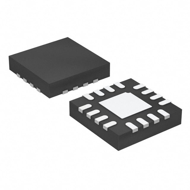
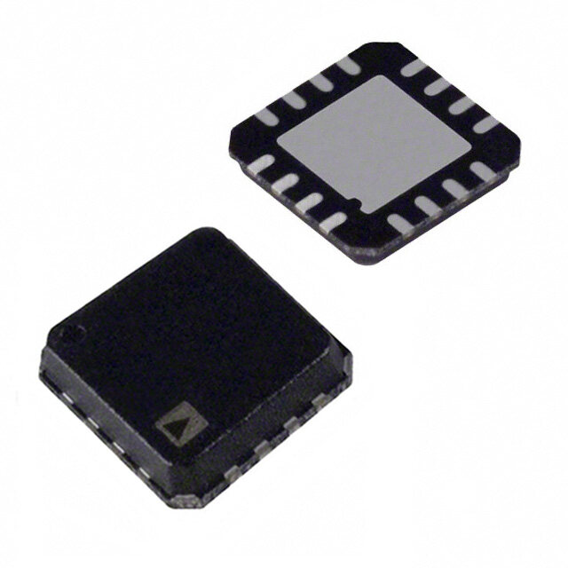
| 供应商器件封装 | 16-WQFN(3x3) |
| 关闭 | Shutdown |
| 其它名称 | 296-25292-1 |
| 制造商产品页 | http://www.ti.com/general/docs/suppproductinfo.tsp?distId=10&orderablePartNumber=TPS54318RTER |
| 包装 | 剪切带 (CT) |
| 同步整流器 | 是 |
| 商标 | Texas Instruments |
| 商标名 | SWIFT |
| 安装类型 | 表面贴装 |
| 安装风格 | SMD/SMT |
| 封装 | Reel |
| 封装/外壳 | 16-WFQFN 裸露焊盘 |
| 封装/箱体 | WQFN-16 |
| 工作温度 | -40°C ~ 150°C |
| 工作温度范围 | - 40 C to + 150 C |
| 工厂包装数量 | 3000 |
| 开关频率 | 2 MHz |
| 拓扑结构 | Buck |
| 最大工作温度 | + 150 C |
| 最大输入电压 | 6 V |
| 最小工作温度 | - 40 C |
| 最小输入电压 | 2.95 V |
| 标准包装 | 1 |
| 电压-输入 | 2.95 V ~ 6 V |
| 电压-输出 | 0.8 V ~ 4.5 V |
| 电流-输出 | 3A |
| 电源电压-最小 | 2.95 V |
| 电源电流 | 350 uA |
| 类型 | 降压(降压) |
| 系列 | TPS54318 |
| 设计资源 | http://www.digikey.com/product-highlights/cn/zh/texas-instruments-webench-design-center/3176 |
| 输入电压 | 2.95 V to 6 V |
| 输出数 | 1 |
| 输出电压 | 0.8 V to 4.5 V |
| 输出电流 | 3 A |
| 输出端数量 | 1 Output |
| 输出类型 | 可调式 |
| 配用 | /product-detail/zh/TPS54318EVM-512/296-25233-ND/2178824 |
| 频率-开关 | 200kHz ~ 2MHz |


- 商务部:美国ITC正式对集成电路等产品启动337调查
- 曝三星4nm工艺存在良率问题 高通将骁龙8 Gen1或转产台积电
- 太阳诱电将投资9.5亿元在常州建新厂生产MLCC 预计2023年完工
- 英特尔发布欧洲新工厂建设计划 深化IDM 2.0 战略
- 台积电先进制程称霸业界 有大客户加持明年业绩稳了
- 达到5530亿美元!SIA预计今年全球半导体销售额将创下新高
- 英特尔拟将自动驾驶子公司Mobileye上市 估值或超500亿美元
- 三星加码芯片和SET,合并消费电子和移动部门,撤换高东真等 CEO
- 三星电子宣布重大人事变动 还合并消费电子和移动部门
- 海关总署:前11个月进口集成电路产品价值2.52万亿元 增长14.8%


PDF Datasheet 数据手册内容提取
Product Order Technical Tools & Support & Folder Now Documents Software Community TPS54318 SLVS975C–SEPTEMBER2009–REVISEDAPRIL2018 TPS54318 2.95-V to 6-V Input, 3-A Output, 2-MHz, Synchronous Step-Down SWIFT™ Converter 1 Features 3 Description • Two,30-mΩ (typical)MOSFETsforHigh- TheTPS54318 device is a full-featured, 6-V, 3-A, 1 synchronous, step-down current-mode converter with Efficiencyat3-Aloads twointegratedMOSFETs. • SwitchingFrequency:200kHzto2MHz The TPS54318 device enables small designs by • VoltageReferenceOverTemperature:0.8V ±1% integrating the MOSFETs, implementing current • SynchronizestoExternalClock mode control to reduce external component count, • AdjustableSoftStart/Sequencing reducing inductor size by enabling up to 2-MHz switching frequency, and minimizing the device • UVandOVPower-GoodOutput footprint with a small, 3 mm x 3 mm, thermally • LowOperatingandShutdownQuiescentCurrent enhanced,QFNpackage. • SafeStart-UpintoPrebiasedOutput The TPS54318 device provides accurate regulation • Cycle-by-CycleCurrentLimit,Thermaland for a variety of loads with an accurate ±1% voltage FrequencyFoldbackProtection reference(V )overtemperature. REF • OperatingJunctionTemperatureRange: –40°Cto Efficiency is maximized through the integrated 30-mΩ 150°C MOSFETs and a 350-μA typical supply current. Using • ThermallyEnhanced3mm×3mm16-pinWQFN the EN pin, shutdown supply current is reduced to 2 Package μAbyenteringashutdownmode. • CreateaCustomDesignUsingtheTPS54318 Undervoltage lockout is internally set at 2.6 V, but WiththeWEBENCH®PowerDesigner can be increased by programming the threshold with a resistor network on the enable pin. The output 2 Applications voltagestartuprampiscontrolledbythesoft-startpin. An open-drain power-good signal indicates the output • Low-Voltage,High-DensityPowerSystems is within 93% to 107% of its nominal voltage. • Point-of-LoadRegulationforHighPerformance Frequency foldback and thermal shutdown protects DSPs,FPGAs,ASICsandMicroprocessors thedeviceduringanovercurrentcondition. • Broadband,NetworkingandOptical For more SWIFT™ documentation, see the TI CommunicationsInfrastructure websiteatwww.ti.com/swift. DeviceInformation(1) PARTNUMBER PACKAGE BODYSIZE(NOM) TPS54318 WQFN(16) 3.00mm×3.00mm (1) For all available packages, see the orderable addendum at theendofthedatasheet. SimplifiedSchematic EfficiencyvsOutputCurrent VIN TPS54318 100 VIN BOOT 95 90 VOUT EN PH 85 %) 80 PWRGD y ( nc 75 e SS VSENSE Effici 70 65 RT/CLK COMP 60 VIN = 5 V GND 55 VOUT = 1.8 V AGND PowerPad 50 fSW = 1 MHz 0 0.5 1 1.5 2 2.5 3 Output Current (A) 1 An IMPORTANT NOTICE at the end of this data sheet addresses availability, warranty, changes, use in safety-critical applications, intellectualpropertymattersandotherimportantdisclaimers.PRODUCTIONDATA.
TPS54318 SLVS975C–SEPTEMBER2009–REVISEDAPRIL2018 www.ti.com Table of Contents 1 Features.................................................................. 1 7.3 FeatureDescription.................................................12 2 Applications........................................................... 1 7.4 DeviceFunctionalModes........................................17 3 Description............................................................. 1 8 ApplicationandImplementation........................ 20 4 RevisionHistory..................................................... 2 8.1 ApplicationInformation............................................20 8.2 TypicalApplication..................................................20 5 PinConfigurationandFunctions......................... 3 9 PowerSupplyRecommendations...................... 30 6 Specifications......................................................... 4 10 Layout................................................................... 30 6.1 AbsoluteMaximumRatings......................................4 6.2 ESDRatings ............................................................4 10.1 LayoutGuidelines.................................................30 6.3 RecommendedOperatingConditions.......................4 10.2 LayoutExample....................................................31 6.4 ThermalInformation..................................................4 11 DeviceandDocumentationSupport................. 32 6.5 ElectricalCharacteristics...........................................5 11.1 DeviceSupport ....................................................32 6.6 TypicalCharacteristics..............................................7 11.2 Trademarks...........................................................32 7 DetailedDescription............................................ 11 11.3 ElectrostaticDischargeCaution............................32 7.1 Overview.................................................................11 11.4 Glossary................................................................32 7.2 FunctionalBlockDiagram.......................................12 12 Mechanical,Packaging,andOrderable Information........................................................... 32 4 Revision History NOTE:Pagenumbersforpreviousrevisionsmaydifferfrompagenumbersinthecurrentversion. ChangesfromRevisionB(December2014)toRevisionC Page • updatetitle ............................................................................................................................................................................. 1 ChangesfromRevisionA(September2013)toRevisionB Page • AddedESDRatingstable,FeatureDescriptionsection,DeviceFunctionalModessection,Applicationand Implementationsection,PowerSupplyRecommendationssection,Layoutsection,DeviceandDocumentation Supportsection,andMechanical,Packaging,andOrderableInformationsection................................................................ 1 ChangesfromOriginal(September2009)toRevisionA Page • Added"Instantaneouspeakcurrent"specificationtotheCurrentLimitsectionintheElectricalCharacteristicstable ........5 • AddedFigure22toTypicalCharacteristicssection............................................................................................................... 9 2 SubmitDocumentationFeedback Copyright©2009–2018,TexasInstrumentsIncorporated ProductFolderLinks:TPS54318
TPS54318 www.ti.com SLVS975C–SEPTEMBER2009–REVISEDAPRIL2018 5 Pin Configuration and Functions RTEPackage 16PinWQFN (TOPVIEW) D G T R O VIN EN PW BO 16 15 14 13 VIN 1 12 PH VIN 2 11 PH Thermal GND 3 Pad 10 PH GND 4 9 SS 5 6 7 8 D E P K N S M L G N O C A E C T/ S R V PinFunctions PIN I/O(1) DESCRIPTION NAME NO. AGND 5 G AnaloggroundshouldbeelectricallyconnectedtoGNDclosetothedevice. AbootstrapcapacitorisrequiredbetweenBOOTandPH.Ifthevoltageonthiscapacitorisbelowthe BOOT 13 I minimumrequiredbytheBOOTUVLO,theoutputisforcedtoswitchoffuntilthecapacitorisrefreshed. Erroramplifieroutput,andinputtotheoutputswitchcurrentcomparator.Connectfrequency COMP 7 O compensationcomponentstothispin. Enablepin,internalpull-upcurrentsource.Pullbelow1.2Vtodisable.Floattoenable.Canbeusedto EN 15 I settheon/offthreshold(adjustUVLO)withtwoadditionalresistors. 3 GND G Powerground.Thispinshouldbeelectricallyconnecteddirectlytothepowerpadunderthedevice. 4 10 Thesourceoftheinternalhigh-sidepowerMOSFET,anddrainoftheinternallow-side(synchronous) PH 11 O rectifierMOSFET. 12 Anopendrainoutput,assertslowifoutputvoltageislowduetothermalshutdown,overcurrent, PWRGD 14 O over/under-voltageorENshutdown. RT/CLK 8 I/O ResistorTimingorExternalClockinputpin. SS 9 I/O Slow-start.Anexternalcapacitorconnectedtothispinsetstheoutputvoltagerisetime.Soft 1 VIN 2 I Inputsupplyvoltage,2.95Vto6V. 16 VSENSE 6 I Invertingnodeofthetransconductance(gm)erroramplifier. GNDpinshouldbeconnectedtotheexposedpowerpadforproperoperation.Thispowerpadshould ThermalPad G beconnectedtoanyinternalPCBgroundplaneusingmultipleviasforgoodthermalperformance. (1) I=Input,O=Output,G=Ground Copyright©2009–2018,TexasInstrumentsIncorporated SubmitDocumentationFeedback 3 ProductFolderLinks:TPS54318
TPS54318 SLVS975C–SEPTEMBER2009–REVISEDAPRIL2018 www.ti.com 6 Specifications 6.1 Absolute Maximum Ratings overoperatingfree-airtemperaturerange(unlessotherwisenoted) (1) MIN MAX UNIT EN,PWRGD,VIN –0.3 7 RT/CLK –0.3 6 Inputvoltage V COMP,SS,VSENSE –0.3 3 BOOT V +8V PH BOOT-PH 8 Outputvoltage PH –0.6 7 V PH(10nstransient) –2 7 Sourcecurrent EN,RT/CLK 100 µA COMP,SS 100 µA Sinkcurrent PWRGD 10 mA Operatingjunctiontemperature,T –40 150 °C J Storagetemperature,T –65 150 °C stg (1) StressesbeyondthoselistedunderAbsoluteMaximumRatingsmaycausepermanentdamagetothedevice.Thesearestressratings only,whichdonotimplyfunctionaloperationofthedeviceattheseoranyotherconditionsbeyondthoseindicatedunderRecommended OperatingConditions.Exposuretoabsolute-maximum-ratedconditionsforextendedperiodsmayaffectdevicereliability. 6.2 ESD Ratings VALUE UNIT Humanbodymodel(HBM),perANSI/ESDA/JEDECJS-001,allpins(1) ±2000 V V(ESD) Electrostaticdischarge Chargeddevicemodel(CDM),perJEDECspecificationJESD22-C101,all pins(2) ±500 V (1) JEDECdocumentJEP155statesthat500-VHBMallowssafemanufacturingwithastandardESDcontrolprocess. (2) JEDECdocumentJEP157statesthat250-VCDMallowssafemanufacturingwithastandardESDcontrolprocess. 6.3 Recommended Operating Conditions overoperatingfree-airtemperaturerange(unlessotherwisenoted) MIN MAX UNIT V Inputvoltage 3 6 V VIN T Operatingjunctiontemperature –40 150 °C J 6.4 Thermal Information(1) TPS54318 THERMALMETRIC(2) RTE(WQFN) UNIT 16PINS R Junction-to-ambientthermalresistance 50 θJA R Junction-to-ambientthermalresistance (3) 37 θJA R Junction-to-case(top)thermalresistance 59.1 θJC(top) R Junction-to-boardthermalresistance 23.1 °C/W θJB ψ Junction-to-topcharacterizationparameter 1.4 JT ψ Junction-to-boardcharacterizationparameter 23.1 JB R Junction-to-case(bottom)thermalresistance 7.9 θJC(bot) (1) Unlessotherwisespecified,metricslistedinthistablerefertoJEDEChigh-Kboardmeasurements (2) Formoreinformationabouttraditionalandnewthermalmetrics,seetheICPackageThermalMetricsapplicationreport,SPRA953. (3) TestBoardConditions: (a)2inches×2inches,4layers,thickness:0.062inch (b)2oz.coppertraceslocatedonthetopofthePCB (c)2oz.coppergroundplaneslocatedonthetwointernallayersandbottomlayer (d)4thermalvias(10mil)locatedunderthedevicepackage 4 SubmitDocumentationFeedback Copyright©2009–2018,TexasInstrumentsIncorporated ProductFolderLinks:TPS54318
TPS54318 www.ti.com SLVS975C–SEPTEMBER2009–REVISEDAPRIL2018 6.5 Electrical Characteristics –40°C≤T ≤150°C,2.95≤V ≤6V(unlessotherwisenoted)overoperatingfree-airtemperaturerange J VIN PARAMETER TESTCONDITIONS MIN TYP MAX UNIT SUPPLYVOLTAGE(VIN) V Operatinginputvoltage 2.95 6 V VIN Internalundervoltagelockout V Novoltagehysteresis,risingandfalling 2.6 2.8 V UVLO threshold I Shutdownsupplycurrent V =0V,T =25°C,2.95V≤V ≤6V 2 5 μA Q(vin) EN A VIN V =0.9V,V =5V,25°C, I Quiescentcurrent VSENSE VIN 350 500 μA q R =400kΩ T ENABLEANDUVLO(EN) Rising 1.16 1.25 1.37 V Enablethreshold V TH(en) Falling 1.18 Enablerisingthreshold+50mV –3.2 I Inputcurrent μA EN Enablefallingthreshold–50mV –0.65 VOLTAGEREFERENCE(VSENSE) V Voltagereference 2.95V≤V ≤6V,–40°C<T <150°C 0.795 0.803 0.811 V REF VIN J MOSFET (V –V )=5V 30 60 BOOT PH R High-sideswitchresistance mΩ DS(HFET) (V –V )=2.95V 44 70 BOOT PH V =5V 30 60 VIN R Low-sideswitchresistance mΩ DS(LFET) V =2.95V 44 70 VIN ERRORAMPLIFIER I Inputcurrent 7 nA IN g Erroramplifiertransconductance –2μA<I <2μA,V =1V 225 μS M(ea) COMP COMP Erroramplifiertransconductance –2μA<I <2μA,V =1V, g COMP COMP 70 μS m(EA,ss) duringsoft-start V =0.4V VSENSE I Erroramplifiersource/sink V =1V,100mVoverdrive ±20 μA COMP COMP COMPtoI g SWITCH 13 A/V M transconductance CURRENTLIMIT I Currentlimitthreshold Instantaneouspeakcurrent 3.7 5.5 A LIM THERMALSHUTDOWN T ThermalShutdown 175 °C SD T Hysteresis 15 °C SD(hyst) TIMINGRESISTORANDEXTERNALCLOCK(RT/CLK) Switchingfrequencyrangeusing f 200 2000 kHz SW RTmode f Switchingfrequency R =400kΩ 400 500 600 kHz SW RT Switchingfrequencyrangeusing f 300 2000 kHz SW CLKmode t MinimumCLKpulsewidth 75 ns MIN(CLK) V RT/CLKvoltage R =400kΩ 0.5 V RT/CLK RT/CLK V RT/CLKhighthreshold 1.6 2.2 V IH(CLK) V RT/CLKlowthreshold 0.4 0.6 V IL(CLK) RT/CLKfallingedgetoPHrising t f =500kHzwithR resistorinseries 90 ns DLY edgedelay SW RT t PLLlock-intime f =500kHz 14 μs LOCK(PLL) SW Copyright©2009–2018,TexasInstrumentsIncorporated SubmitDocumentationFeedback 5 ProductFolderLinks:TPS54318
TPS54318 SLVS975C–SEPTEMBER2009–REVISEDAPRIL2018 www.ti.com Electrical Characteristics (continued) –40°C≤T ≤150°C,2.95≤V ≤6V(unlessotherwisenoted)overoperatingfree-airtemperaturerange J VIN PARAMETER TESTCONDITIONS MIN TYP MAX UNIT HIGH-SIDEPOWERMOSFET(PH) Measuredat50%pointsonPH,I =3 60 OUT tON(min) Minimumontime Measuredat50%pointsonPH,VVIN=5V, 110 ns I =0A OUT Priortoskippingoffpulses, t Minimumofftime 60 ns OFF(min) (V –V )=2.95V,I =3 BOOT PH OUT t Risetime V =5V 1.5 V/ns RISE VIN t Falltime V =5V 1.5 V/ns FALL VIN BOOT(BOOT) R BOOTchargeresistance V =5V 16 Ω BOOT VIN V BOOT-PHUVLO V =2.95V 2.1 V UVLO(Boot) VIN SOFT-START(SS) I Chargecurrent V =0.4V 1.8 μA CHG SS V SStoreferencecrossover 98%nominal 0.9 V SSxREF V SSdischargevoltage(overload) V =0V 20 μA DSCHG(SS) VSENSE SSdischargecurrent(UVLO, I V =5V,V =0.5V 1.25 mA DSCHG(SS) EN,thermalfault) VIN SS POWERGOOD(PWRGD) V falling(fault) 91% VSENSE V rising(good) 93% VSENSE V VSENSEthreshold TH(PG) V rising(fault) 107% V VSENSE REF V falling(Good) 105% VSENSE V Hysteresis V falling 2% HYST(PG) VSENSE I Outputhighleakage V =V ,V =5.5V 2 nA PH(lkg) VSENSE REF PWRGD R PowerGoodon-resistance 100 Ω PG V Low-leveloutputvoltage I =3.5mA 0.3 V OL PWRGD Minimuminputvoltageforvalid V V <0.5V,I =100μA 1.2 1.6 V MIN(PG) output PWRGD OUT 6 SubmitDocumentationFeedback Copyright©2009–2018,TexasInstrumentsIncorporated ProductFolderLinks:TPS54318
TPS54318 www.ti.com SLVS975C–SEPTEMBER2009–REVISEDAPRIL2018 6.6 Typical Characteristics W 0.055 550 e - High Side Rdson RT= 400 kW, sistanc 0.05 LowV IS=id 3e. 3R dVson VI= 3.3 V Hz553400 VI= 3.3 V e k On-State R 0.00.4045 HighV SIi=d e5 RVdson equency - 551200 urce ng Fr500 atic Drain-So 0.00.3035 Low VSIid=e 5 R Vdson f- Switchis444789000 N - St 0.025 460 O S D 0.02 450 R -50 -25 0 25 50 75 100 125 150 -50 -25 0 25 50 75 100 125 150 TJ- Junction Temperature - °C TJ- Junction Temperature - °C Figure1.High-SideandLow-SideOnResistancevs Figure2.FrequencyvsJunctionTemperature JunctionTemperature 6 0.808 5.9 VIN= 3 V VIN= 3 .3 V 0.806 5.8 A V 0.804 Current - 55..67 erence - 0.802 ch 5.5 Ref 0.8 wit ge High Side S 555...234 V- Voltaref00..779968 0.794 5.1 5 0.792 -50 -25 0 25 50 75 100 125 150 -50 -25 0 25 50 75 100 125 150 TJ- Junction Temperature - °C TJ- Junction Temperature - °C Figure3.High-SideCurrentLimitvsJunctionTemperature Figure4.VoltageReferencevsJunctionTemperature 1000 2000 1900 900 1800 Hz 800 kHz witching Frequncy - k 567000000 witching Frequency - 11111345670000000000 f-Ss400 f- Ss1200 300 1100 200 1000 100 200 300 400 500 600 700 800 900 1000 80 100 120 140 160 180 200 RT - Resistance - kW RT - Resistance kW Figure5. SwitchingFrequencyvsRTResistanceLow Figure6.SwitchingFrequencyvsRTResistanceHigh FrequencyRange FrequencyRange Copyright©2009–2018,TexasInstrumentsIncorporated SubmitDocumentationFeedback 7 ProductFolderLinks:TPS54318
TPS54318 SLVS975C–SEPTEMBER2009–REVISEDAPRIL2018 www.ti.com Typical Characteristics (continued) 100 280 Vsense Falling 260 VIN= 3 .3 V % ncy - 75 A/Vm 240 ng Freque 50 Vsense Rising ductance - 220 Switchi anscon 200 Normal 25 EA- Tr 180 160 140 00 0.1 0.2 0.3 0.4 0.5 0.6 0.7 0.8 -50 -25 0 25 50 75 100 125 150 Vsense - V TJ- Junction Temperature - °C Figure7.SwitchingFrequencyvsVsense Figure8.TransconductancevsJunctionTemperature 90 1.3 85 VIN= 3 .3 V 1.29 1.28 80 1.27 VIN= 3.3 V, rising A/V 75 1.26 ce -m 70 d - V 11..2245 uctan 65 eshol 1.23 - Transcond 5650 EN - Thr 1111...122.2912 VIN= 3.3 V, falling EA 50 1.18 1.17 45 1.16 40 1.15 -50 -25 0 25 50 75 100 125 150 -50 -25 0 25 50 75 100 125 150 TJ- Junction Temperature - °C TJ- Junction Temperature - °C Figure9.Transconductance(Soft-Start)vsJunction Figure10.EnablePinVoltagevsJunctionTemperature Temperature -2.75 -0.25 -2.85 VVIENN== 5R Vis,ingThreshold +50 mV -0.35 VVIENN== 5 F Va,llingThreshold -50 mV -2.95 -0.45 -3.05 A -0.55 A m Current -m --33..2155 n Current - --00..7655 n -3.35 Pi -0.85 EN Pi -3.45 EN - -0.95 -3.55 -1.05 -3.65 -1.15 -1.25 -3.75-50 -25 0 25 50 75 100 125 150 -50 -25 0 25 50 75 100 125 150 TJ- Junction Temperature - °C TJ- Junction Temperature - °C Figure11.PinCurrentvsJunctionTemperature Figure12. PinCurrentvsJunctionTemperature 8 SubmitDocumentationFeedback Copyright©2009–2018,TexasInstrumentsIncorporated ProductFolderLinks:TPS54318
TPS54318 www.ti.com SLVS975C–SEPTEMBER2009–REVISEDAPRIL2018 Typical Characteristics (continued) -1 105 -1.2 103 A-1.4 Am101 VIN= 5 V nt -m-1.6 VIN= 5 V ent - 99 urre-1.8 Curr 97 e C -2 ge 95 arg har Ch-2.2 sc 93 S/TR - -2.4 TR - Di 91 S-2.6 SS/ 89 -2.8 87 -3 85 -50 -25 0 25 50 75 100 125 150 -50 -25 0 25 50 75 100 125 150 TJ- Junction Temperature - °C TJ- Junction Temperature - °C Figure13.ChargeCurrentvsJunctionTemperature Figure14.DischargeCurrentvsJunctionTemperature 3 3 2.9 VIN= 3.3 V 2.5 2.8 A m V- Input Voltage - VIN 22222.....34567 UVULVOL OS tSopta Srtw Sitwcihtcinhging down Supply Current -1.512 ut h 2.2 S 0.5 2.1 2 0 -50 -25 0 25 50 75 100 125 150 -50 -25 0 25 50 75 100 125 150 TJ- Junction Temperature - °C TJ- Junction Temperature - °C Figure15.InputVoltagevsJunctionTemperature Figure16.ShutdownSupplyCurrentvsJunction Temperature 3 400 TJ= 25°C 390 VIN= 3.3 V 2.5 380 A m A upply Current1.52 ply Current -m 333567000 hutdown S 1 I- SupCC333400 S 320 0.5 310 0 300 3 3.5 4 4.5 5 5.5 6 -50 -25 0 25 50 75 100 125 150 VIN- Input Voltage - V TJ- Junction Temperature - °C Figure17.ShutdownSupplyCurrentvsInputVoltage Figure18. SupplyCurrentvsJunctionTemperature Copyright©2009–2018,TexasInstrumentsIncorporated SubmitDocumentationFeedback 9 ProductFolderLinks:TPS54318
TPS54318 SLVS975C–SEPTEMBER2009–REVISEDAPRIL2018 www.ti.com Typical Characteristics (continued) 400 110 390 TJ= 25°C 108 Vsense Rising, VIN= 3.3 V 380 106 Am 370 % Vref 104 Vsense Falling Supply Current - 333456000 D - Threshold - 1100990268 - CC330 WRG 94 Vsense Rising I P 320 92 310 90 Vsense Falling 300 88 3 3.5 4 4.5 5 5.5 6 -50 -25 0 25 50 75 100 125 150 VIN- Input Voltage - V TJ- Junction Temperature - °C Figure19.SupplyCurrentvsInputVoltage Figure20.PWRGDThresholdvsJunctionTemperature W 200 1 nce - 180 VIN= 3.3 V 0.9 –3 Sigma a Typical sist 160 0.8 e +3 Sigma n State R 112400 age (V) 00..67 ec O 100 Volt 0.5 Sour 80 MP 0.4 Drain- 60 CO 0.3 c 0.2 ati 40 St 0.1 N - 20 O 0 S D 0 -50 -25 0 25 50 75 100 125 150 R -50 -25 0 25 50 75 100 125 150 TJ- Junction Temperature - °C Junction Temperature (°C) Figure21.PWRGDOnResistancevsJunctionTemperature Figure22.MinimumCompVoltageClampvsJunction Temperature 10 SubmitDocumentationFeedback Copyright©2009–2018,TexasInstrumentsIncorporated ProductFolderLinks:TPS54318
TPS54318 www.ti.com SLVS975C–SEPTEMBER2009–REVISEDAPRIL2018 7 Detailed Description 7.1 Overview The TPS54318 device is a 6-V, 3-A, synchronous step-down (buck) converter with two integrated n-channel MOSFETs. To improve performance during line and load transients the device implements a constant frequency, peak current mode control which reduces output capacitance and simplifies external frequency compensation design. The wide supported switching frequency range of 200 kHz to 2000 kHz allows for efficiency and size optimization when selecting the output filter components. The switching frequency is adjusted using a resistor to ground on the RT/CLK pin. The device has an internal phase lock loop (PLL) on the RT/CLK pin that is used to synchronizethepowerswitchturnontoafallingedgeofanexternalsystemclock. The TPS54318 device has a typical default start up voltage of 2.6 V. The EN pin has an internal pull-up current source that can be used to adjust the input voltage under voltage lockout (UVLO) with two external resistors. In addition, the pull up current provides a default condition when the EN pin is floating for the device to operate. The total operating current for the TPS54318 device is 350 μA when not switching and under no load. When the deviceisdisabled,thesupplycurrentislessthan5μA. The integrated, 30-mΩ MOSFETs allow for high-efficiency power supply designs with continuous output currents upto3amperes. The TPS54318 device reduces the external component count by integrating the boot recharge diode. The bias voltage for the integrated high-side MOSFET is supplied by a capacitor on the BOOT to PH pin. The boot capacitor voltage is monitored by an UVLO circuit and turns off the high-side MOSFET when the voltage falls below a preset threshold. This BOOT circuit allows the TPS54318 device to operate approaching 100%. The outputvoltagecanbesteppeddowntoaslowasthe0.8Vreference. TheTPS54318devicehasapowergoodcomparator(PWRGD)with2%hysteresis. The TPS54318 device minimizes excessive output overvoltage transients by taking advantage of the overvoltage power good comparator. When the regulated output voltage is greater than 109% of the nominal voltage, the overvoltage comparator is activated, and the high-side MOSFET is turned off and masked from turning on until theoutputvoltageislowerthan105%. The SS (soft-start) pin is used to minimize inrush currents or provide power supply sequencing during power up. A small value capacitor should be coupled to the pin for soft-start. The SS pin is discharged before the output poweruptoensurearepeatablere-startafteranover-temperaturefault,UVLOfaultordisabledcondition. The use of a frequency-foldback circuit reduces the switching frequency during startup and over current fault conditionstohelplimittheinductorcurrent. Copyright©2009–2018,TexasInstrumentsIncorporated SubmitDocumentationFeedback 11 ProductFolderLinks:TPS54318
TPS54318 SLVS975C–SEPTEMBER2009–REVISEDAPRIL2018 www.ti.com 7.2 Functional Block Diagram PWRGD EN VIN Thermal i1 iHYS Shutdown UVLO 93% Logic Enable Comparator 107% Shutdown Boot Logic Charge Voltage Reference Enable Boot Threshold UVLO VSENSE + + BOOT SS Minimum Shutdown COMP Clamp Logic PWM Comparator Logic and COMP PWM Latch PH (cid:8) Slope Compensation Frequency GND Shift Overload Maximum OSC with Recovery Clamp PLL AGND PowerPad RT/CLK 7.3 Feature Description 7.3.1 FixedFrequencyPWMControl The TPS54318 device uses an adjustable fixed-frequency peak-current-mode control. The output voltage is compared through external resistors on the VSENSE to pin an internal voltage reference by an error amplifier which drives the COMP pin. An internal oscillator initiates the turnon of the high-side power switch. The error amplifier output is compared to the high-side power-switch current. When the power switch reaches the COMP voltage,thehigh-sidepowerswitchisturnedoffandthelow-sidepowerswitchisturnedon. The COMP pin voltage increases and decreases as the peak switch current increases and decreases. The device implements a current-limit function by clamping the COMP pin voltage to a maximum value, which limits the maximum peak current the device supplies. The device also implements a minimum COMP pin voltage clamp for improved transient response. When the COMP pin voltage is pushed low to the minimum clamp, such asduringaloadreleaseevent,turn-onofthehigh-sidepowerswitchisinhibited. 7.3.2 SlopeCompensationandOutputCurrent The TPS54318 device adds a compensating ramp to the switch current signal. This slope compensation preventssub-harmonicoscillationsasdutycycleincreases.Theavailablepeakinductorcurrentremainsconstant overthefulldutycyclerange. 7.3.3 BootstrapVoltage(Boot)andLowDropoutOperation The TPS54318 device has an integrated boot regulator and requires a small ceramic capacitor between the BOOT and PH pin to provide the gate drive voltage for the high-side MOSFET. The value of the ceramic capacitorshouldbe0.1μF.AceramiccapacitorwithanX7RorX5Rgradedielectricwithavoltageratingof10V orhigherisrecommendedbecauseofthestablecharacteristicsovertemperatureandvoltage. 12 SubmitDocumentationFeedback Copyright©2009–2018,TexasInstrumentsIncorporated ProductFolderLinks:TPS54318
TPS54318 www.ti.com SLVS975C–SEPTEMBER2009–REVISEDAPRIL2018 Feature Description (continued) To improve drop out, the TPS54318 device is designed to operate at 100% duty cycle as long as the BOOT to PH pin voltage is greater than 2.5 V. The high-side MOSFET is turned off using an UVLO circuit, allowing for the low-sideMOSFETtoconductwhenthevoltagefromBOOTtoPHdropsbelow2.5V.Becausethesupplycurrent sourced from the BOOT pin is low, the high-side MOSFET can remain on for more switching cycles than are requiredtorefreshthecapacitor,thustheeffectivedutycycleoftheswitchingregulatorishigh. 7.3.4 ErrorAmplifier The TPS54318 device has a transconductance amplifier. The error amplifier compares the VSENSE voltage to the lower of the SS pin voltage or the internal 0.8 V voltage reference. The transconductance of the error amplifier is 225 μA/V during normal operation. When the voltage of VSENSE pin is below 0.8 V and the device is regulating using the SS voltage, the transconductance is 70 μA/V. The frequency compensation components are placedbetweentheCOMPpinandground. 7.3.5 VoltageReference The voltage reference system produces a precise ±1% voltage reference overtemperature by scaling the output of a temperature stable bandgap circuit. The bandgap and scaling circuits produce 0.8 V at the non-inverting inputoftheerroramplifier. 7.3.6 AdjustingtheOutputVoltage The output voltage is set with a resistor divider from the output node to the VSENSE pin. It is recommended to use divider resistors with 1% tolerance or better. Start with a value of 100 kΩ for the R1 resistor and use Equation 1 to calculate R2. To improve efficiency at very light loads, consider using larger resistor values. If the values are too high, the regulator is more susceptible to noise and voltage errors from the VSENSE input current arenoticeable. æ 0.8 V ö R2= R1 ´ ç ÷ èVO - 0.8V ø (1) VOUT R1 VSENSE + 0.8 V R2 Figure23. VoltageDividerCircuit 7.3.7 EnableandAdjustingUndervoltageLockout The TPS54318 device is disabled when the VIN pin voltage falls below 2.6 V. If an application requires a higher under-voltage lockout (UVLO), use the EN pin as shown in Figure 24 to adjust the input voltage UVLO by using two external resistors. It is recommended to use the enable resistors to set the UVLO falling threshold (V ) STOP above 2.7 V. The rising threshold (V ) should be set to provide enough hysteresis to allow for any input START supply variations. The EN pin has an internal pull-up current source that provides the default condition of the TPS54318 device operating when the EN pin floats. Once the EN pin voltage exceeds 1.25 V, an additional 2.55 μA of hysteresis is added. When the EN pin is pulled below 1.18 V, the 2.55 μA is removed. This additional currentfacilitatesinputvoltagehysteresis. Copyright©2009–2018,TexasInstrumentsIncorporated SubmitDocumentationFeedback 13 ProductFolderLinks:TPS54318
TPS54318 SLVS975C–SEPTEMBER2009–REVISEDAPRIL2018 www.ti.com Feature Description (continued) VIN I1 IHYS 0.6 µA 2.55 µA R1 EN + R2 Figure24. AdjustableUndervoltageLockout 0.944×V -V R1= START STOP 2.59´10-6 (2) 1.18×R1 R2 = V -1.18+R1×3.2´10-6 STOP (3) 7.3.8 Soft-StartPin The TPS54318 device regulates to the lower of the SS pin and the internal reference voltage. A capacitor on the SS pin to ground implements a soft-start time. The TPS54318 device has an internal pull-up current source of 1.8 μA which charges the external soft-start capacitor. Equation 4 calculates the required soft-start capacitor value where t is the desired soft-start time in ms, I is the internal soft-start charging current of 1.8 μA, and SS SS V is the internal voltage reference of 0.8 V. it is recommended to maintain the soft-start time in the range REF between1msand10ms. I ´t C = SS SS SS V REF where • C isinnF SS • t isinms SS • I isinµA SS • V isinV (4) REF If during normal operation, the input voltage goes below the UVLO, EN pin pulled below 1.2 V, or a thermal shutdown event occurs, the TPS54318 device stops switching and the SS is discharged to 0 volts before reinitiatingapoweringupsequence. 7.3.9 Sequencing Many of the common power supply sequencing methods can be implemented using the SS, EN and PWRGD pins. The sequential method can be implemented using an open drain or collector output of a power on reset pin of another device. Figure 25 shows the sequential method. The power good is coupled to the EN pin on theTPS54318devicewhichenablesthesecondpowersupplyoncetheprimarysupplyreachesregulation. Ratiometric start up can be accomplished by connecting the SS pins together. The regulator outputs ramp up and reach regulation at the same time. When calculating the soft-start time the pull up current source must be doubledinEquation4.TheratiometricmethodisshowninFigure27. 14 SubmitDocumentationFeedback Copyright©2009–2018,TexasInstrumentsIncorporated ProductFolderLinks:TPS54318
TPS54318 www.ti.com SLVS975C–SEPTEMBER2009–REVISEDAPRIL2018 Feature Description (continued) TPS54318 TPS54318 EN1 = 2 V / div PWRGD EN EN PWRGD SS SS/TR PWRGD1 = 2 V / div CSS CSS Vout1 = 1 / div Vout2 = 1 V / div Time = 5 msec / div Figure25.SequencialStart-UpSchematic Figure26.SequentialStartupusingENand PWRGD TPS54318 TPS54318 EN1 = 2 V / div EN EN SS SS Vout1 = 1 V / div CSS PWRGD PWRGD Vout2 = 1 V / div Time = 5 msec / div Figure27.RatiometricStart-UpSchematic Figure28.RatiometricStart-UpUsingCoupledSS Pins 7.3.10 ConstantSwitchingFrequencyandTimingResistor(RT/CLKPin) The switching frequency of the TPS54318 device is adjustable over a wide range from 200 kHz to 2000 kHz by placing a maximum of 1000 kΩ and minimum of 85 kΩ, respectively, on the RT/CLK pin. An internal amplifier holds this pin at a fixed voltage when using an external resistor to ground to set the switching frequency. The RT/CLK is typically 0.5 V. To determine the timing resistance for a given switching frequency, use the curve in Figure5 orFigure6orEquation5. 311890 RRT = 1.0793 (f ) SW where • R isinkΩ RT • f isinkHz (5) SW 133870 fSW = 0.9393 (R ) RT where • R isinkΩ RT • f isinkHz (6) SW To reduce the solution size one would typically set the switching frequency as high as possible, but tradeoffs of theefficiency,maximuminputvoltageandminimumcontrollableontimeshouldbeconsidered. Copyright©2009–2018,TexasInstrumentsIncorporated SubmitDocumentationFeedback 15 ProductFolderLinks:TPS54318
TPS54318 SLVS975C–SEPTEMBER2009–REVISEDAPRIL2018 www.ti.com Feature Description (continued) The minimum controllable on time is typically 60 ns at full current load and 110 ns at no load, and limits the maximumoperatinginputvoltageoroutputvoltage. 7.3.11 OvercurrentProtection TheTPS54318deviceimplementsacycle-by-cyclecurrentlimit.Duringeachswitchingcyclethehigh-sideswitch current is compared to the voltage on the COMP pin. When the instantaneous switch current intersects the COMP voltage, the high-side switch is turned off. During overcurrent conditions that pull the output voltage low, the error amplifier responds by driving the COMP pin high, increasing the switch current. The error amplifier outputisclampedinternally.Thisclampfunctionsasaswitchcurrentlimit. 7.3.12 FrequencyShift To operate at high switching frequencies and provide protection during overcurrent conditions, the TPS54318 device implements a frequency shift. If frequency shift was not implemented, during an overcurrent condition the low-side MOSFET may not be turned off long enough to reduce the current in the inductor, causing a current runaway. With frequency shift, during an overcurrent condition the switching frequency is reduced from 100%, then 75%, then 50%, then 25% as the voltage decreases from 0.8 to 0 volts on VSENSE pin to allow the low- side MOSFET to be off long enough to decrease the current in the inductor. During start-up, the switching frequencyincreasesasthevoltageonVSENSEincreasesfrom0to0.8volts.SeeFigure7 fordetails. 7.3.13 ReverseOvercurrentProtection The TPS54318 device implements low-side current protection by detecting the voltage across the low-side MOSFET. When the converter sinks current through its low-side FET, the control circuit turns off the low-side MOSFET if the reverse current is more than 1.3 A. By implementing this additional protection scheme, the converter is able to protect itself from excessive current during power cycling and start-up into pre-biased outputs. 7.3.14 SynchronizeUsingtheRT/CLKPin The RT/CLK pin is used to synchronize the converter to an external system clock. See Figure 29. To implement the synchronization feature in a system, connect a square wave to the RT/CLK pin with an on time of at least 75ns. If the pin is pulled above the PLL upper threshold, a mode change occurs and the pin becomes a synchronization input. The internal amplifier is disabled and the pin is a high impedance clock input to the internalPLL.Ifclockingedgesstop,theinternalamplifierisre-enabledandthemodereturnstothefrequencyset by the resistor. The square wave amplitude at this pin must transition lower than 0.6 V and higher than 1.6 V typically. The recommended synchronization frequency range is 300 kHz to 2000 kHz. If the external system clockistoberemoved,TIrecommendsthatitberemovedonthefallingedgeoftheclock. . . SYNC Clock = 2 V / div RT/CLK PLL RRT PH = 2 V / div Time = 500 nsec / div Figure29.SynchronizingtoaSystemClock Figure30.PlotofSynchronizingtoSystemClock 16 SubmitDocumentationFeedback Copyright©2009–2018,TexasInstrumentsIncorporated ProductFolderLinks:TPS54318
TPS54318 www.ti.com SLVS975C–SEPTEMBER2009–REVISEDAPRIL2018 Feature Description (continued) 7.3.15 PowerGood(PWRGDPin) The PWRGD pin output is an open drain MOSFET. The output is pulled low when the VSENSE voltage enters the fault condition by falling below 91% or rising above 107% of the nominal internal reference voltage. There is a 2% hysteresis on the threshold voltage, so when the VSENSE voltage rises to the good condition above 93% or falls below 105% of the internal voltage reference the PWRGD output MOSFET is turned off. It is recommended to use a pull-up resistor between the values of 1 kΩ and 100 kΩ to a voltage source that is 6 V or less.ThePWRGDisinavalidstateoncetheVINinputvoltageisgreaterthan1.2V. 7.3.16 OvervoltageTransientProtection The TPS54318 device incorporates an overvoltage transient protection (OVTP) circuit to minimize voltage overshoot when recovering from output fault conditions or strong unload transients. The OVTP feature minimizes the output overshoot by implementing a circuit to compare the VSENSE pin voltage to the OVTP threshold which is 109% of the internal voltage reference. If the VSENSE pin voltage is greater than the OVTP threshold, the high-side MOSFET is disabled preventing current from flowing to the output and minimizing output overshoot. When the VSENSE voltage drops lower than the OVTP threshold the high-side MOSFET is allowed to turn on thenextclockcycle. 7.3.17 ThermalShutdown The device implements an internal thermal shutdown to protect itself if the junction temperature exceeds 175°C. The thermal shutdown forces the device to stop switching when the junction temperature exceeds the thermal trip threshold. Once the die temperature decreases below 160°C, the device reinitiates the power up sequence bydischargingtheSSpinto0volts.Thethermalshutdownhysteresisis15°C. 7.4 Device Functional Modes 7.4.1 SmallSignalModelforLoopResponse Figure 31 shows an equivalent model for the TPS54318 device control loop which can be modeled in a circuit simulation program to check frequency response and dynamic load response. The error amplifier is a transconductance amplifier with a g of 225 μA/V. The error amplifier can be modeled using an ideal voltage M controlled current source. The resistor R and capacitor C model the open loop gain and frequency OUT(ea) OUT(ea) response of the amplifier. The 1-mV AC voltage source between the nodes a and b effectively breaks the control loop for the frequency response measurements. Plotting a/c shows the small signal response of the frequency compensation. Plotting a/b shows the small signal response of the overall loop. The dynamic loop response can be checked by replacing the R with a current source with the appropriate load step amplitude and step rate LOAD inatimedomainanalysis. PH Power Stage VOUT 13 A/V a R ESR b R1 R LOAD VSENSE C COMP OUT c + 0.8 V R2 C2 R3 COUT(ea) R gM OUT(ea) 225 µA/V C1 Figure31. SmallSignalModelforLoopResponse Copyright©2009–2018,TexasInstrumentsIncorporated SubmitDocumentationFeedback 17 ProductFolderLinks:TPS54318
TPS54318 SLVS975C–SEPTEMBER2009–REVISEDAPRIL2018 www.ti.com Device Functional Modes (continued) 7.4.2 SimpleSmallSignalModelforPeakCurrentModeControl Figure 32 is a simple small signal model that can be used to understand how to design the frequency compensation. The TPS54318 device power stage can be approximated to a voltage controlled current source (duty cycle modulator) supplying current to the output capacitor and load resistor. The control to output transfer function is shown in Equation 7 and consists of a dc gain, one dominant pole and one ESR zero. The quotient of the change in switch current and the change in COMP pin voltage (node c in Figure 31) is the power stage transconductance. The g for the TPS54318 device is 13 A/V. The low frequency gain of the power stage M frequency response is the product of the transconductance and the load resistance as shown in Equation 8. As the load current increases and decreases, the low frequency gain decreases and increases, respectively. This variation with load may seem problematic at first glance, but the dominant pole moves with load current [see Equation 9]. The combined effect is highlighted by the dashed line in the right half of Figure 33. As the load current decreases, the gain increases and the pole frequency lowers, keeping the 0-dB crossover frequency the sameforthevaryingloadconditionswhichmakesiteasiertodesignthefrequencycompensation. VC RESR RLOAD Adc gM(PS) COUT n ai G fP fZ Frequency Figure32.SimpleSmallSignalModel Figure33.FrequencyResponse æ s ö 1+ç ÷ VOUT = Adc´ è2p´fZ ø V æ s ö C 1+ç ÷ è2p´fP ø (7) Adc =g ´R M(PS) LOAD (8) 1 f = P C ´R ´2p OUT LOAD (9) 1 f = Z C ´R ´2p OUT ESR (10) 7.4.3 SmallSignalModelforFrequencyCompensation The TPS54318 device uses a transconductance amplifier for the error amplifier and readily supports two of the commonly used frequency compensation circuits. The compensation circuits are shown in Figure 34. The Type-II circuits are most likely implemented in high bandwidth power supply designs using low ESR output capacitors. In Type-IIA,oneadditionalhighfrequencypoleisaddedtoattenuatehigh-frequencynoise. 18 SubmitDocumentationFeedback Copyright©2009–2018,TexasInstrumentsIncorporated ProductFolderLinks:TPS54318
TPS54318 www.ti.com SLVS975C–SEPTEMBER2009–REVISEDAPRIL2018 Device Functional Modes (continued) VOUT R1 VSENSE COMP gM(ea) + VREF R2 R3 C2 R3 C1 C1 C5 OpUFT(ea) ROUT(ea) Type IIB Type IIA Figure34. TypesofFrequencyCompensation ThedesignguidelinesforTPS54318deviceloopcompensationareasfollows: 1. Calculate the modulator pole (f ) and the esr zero, (f ) using Equation 11and Equation 12. If the output P(MOD) Z1 voltage is a high percentage of the capacitor rating it may be necessary to derate the output capacitor (C ). Use the capacitor manufacturer information to derate the capacitor value. Use Equation 13 and OUT Equation 14 to estimate a starting point for the crossover frequency, f . Equation 13 shows the geometric C mean of the modulator pole and the ESR zero and Equation 14 is the mean of modulator pole and the switching frequency. Use the lower value of Equation 13 or Equation 14 as the maximum crossover frequency. I OUT(max) f = P(mod) 2p´VOUT´COUT (11) 1 f = Z1 C ×R ×tN OUT ESR (12) f = f +f C P:mod; Z1 § (13) f fC = fP(mod)´ S2W (14) 2. CalculateresistorR3.Equation15showsthecalculationforresistorR3. 2p´f ´V ´C R3= C OUT OUT g ´V ´g M(ea) REF M(ps) where • g istheamplifiergain(225μA/V) M(ea) • g isthepowerstagegain(13A/V) (15) M(ps) 3. Placeacompensationzeroatthedominantpole.f .Equation16showsthecalculationforcapacitorC1. P 1 f = P C ´R ´2p OUT LOAD (16) R ´ C C1= L OUT R3 (17) 4. CapacitorC2isoptional.Itcanbeusedtocancelthezerofromtheoutputcapacitor(C )ESR. OUT R ´ C C2= ESR OUT R3 (18) Copyright©2009–2018,TexasInstrumentsIncorporated SubmitDocumentationFeedback 19 ProductFolderLinks:TPS54318
TPS54318 SLVS975C–SEPTEMBER2009–REVISEDAPRIL2018 www.ti.com 8 Application and Implementation NOTE Information in the following applications sections is not part of the TI component specification, and TI does not warrant its accuracy or completeness. TI’s customers are responsible for determining suitability of components for their purposes. Customers should validateandtesttheirdesignimplementationtoconfirmsystemfunctionality. 8.1 Application Information Thisdesignexampledescribesahigh-frequencyswitchingregulatordesignusingceramicoutputcapacitors.This designisavailableasthe HPA512(SLVU330)evaluationmodule(EVM). 8.2 Typical Application Thissectiondetailsahigh-frequency,1.8-VoutputpowersupplydesignapplicationwithadjustedUVLO. U1 L1 TPS54318RTE 1.5 (cid:29)H VOUT = 1.8 V VIN = 3 V to 6 V 16 IOUT = 3 A 10 VIN 1 VIN PH VOUT 11 VIN PH C5 R1 2 12 0.1 PF 48.7 N(cid:159) VIN PH R6 C1 C2 15 13 R5 C6 C7 C8 100 N(cid:159) 10 PF 0.1 PF EN BOOT 100 N(cid:159)(cid:3) 22 PF 22 PF 22 PF 6 14 R322.4 N(cid:159)VSNS 7 VSNS PWRGD 3 VIN VSNS COMP GND R7 8 4 PWRGD 80.6 N(cid:159) RT/CLK GND R3 R4 14.3 N(cid:159) 182 N(cid:159) AGND 5 9 SS C3 2700 pF PowerPAD C4 0.01 PF Figure35. TypicalApplicationSchematic,TPS54318 8.2.1 DesignRequirements Table1.DesignParameters PARAMETER NOTESANDCONDITIONS MIN TYP MAX UNIT V Inputvoltage Operating 3 3.3 6 IN V Startinputvoltage Rising 3.1 V START V Stopinputvoltage Falling 2.8 STOP V Outputvoltage 1.8 V OUT ΔV Transientresponse 1-Ato2-Aloadstep 3% OUT I Maximumoutputcurrent 3 A OUT(max) V Outputvoltageripple 30 mV OUT(ripple) P-P f Switchingfrequency 1 MHz SW 20 SubmitDocumentationFeedback Copyright©2009–2018,TexasInstrumentsIncorporated ProductFolderLinks:TPS54318
TPS54318 www.ti.com SLVS975C–SEPTEMBER2009–REVISEDAPRIL2018 8.2.2 DetailedDesignProcedure 8.2.2.1 StepOne:SelecttheSwitchingFrequency Choose the highest switching frequency possible in order to produce the smallest solution size. The high switching frequency allows for lower valued inductors and smaller output capacitors compared to a power supply that switches at a lower frequency. However, the highest switching frequency causes extra switching losses, whichinturndecreasethedeviceperformance. Thedeviceiscapableofoperatingbetween200kHzand2MHz. Select a moderate switching frequency of 1 MHz in order to achieve both a small solution size and a high- efficiency operation. Using Equation 5, R4 is calculates to 180 kΩ. A standard 1%, 182-kΩ resistor is used in the design. 8.2.2.2 StepTwo:SelecttheOutputInductor The inductor selected must operate across the entire TPS54318 device input voltage range. To calculate the value of the output inductor, use Equation 19. K is a coefficient that represents the amount of inductor ripple IND current relative to the maximum output current. The inductor ripple current is filtered by the output capacitor. Therefore, choosing high inductor ripple currents impacts the selection of the output capacitor since the output capacitor must have a ripple current rating equal to or greater than the inductor ripple current. In general, the inductor ripple value is at the discretion of the designer; however, K is normally from 0.1 to 0.3 for the majority IND ofapplications. For this design example, use a K of 0.3 and the inductor value is calculated to be 1.40 μH. For this design, IND use an inductor with the nearest standard value of 1.50 μH. For the output filter inductor, it is important that the RMS current and saturation current ratings not be exceeded. The RMS and peak inductor current can be calculatedinEquation21andEquation22. For this design, the RMS inductor current is 3.01 A and the peak inductor current is 3.42 A. The chosen inductor is a Coilcraft XPL7030-152ML. It has a RMS current rating of 12.3 A and a saturation current rating of 20.2 A. The current ratings for this exceed the requirement, but the inductor was chosen for small physical size and low seriesresistanceforhighefficiency. The current flowing through the inductor is the inductor ripple current plus the output current. During power up, faults or transient load conditions, the inductor current can increase above the calculated peak inductor current level calculated above. In transient conditions, the inductor current can increase up to the switch current limit of the device. For this reason, the most conservative approach is to specify an inductor with a saturation current ratingequaltoorgreaterthantheswitchcurrentlimitratherthanthepeakinductorcurrent. ( ) VIN(max)-VOUT V L1= ´ OUT IOUT´KIND VIN(max)´fSW (19) ( ) VIN(max)-VOUT V IRIPPLE = ´ OUT L1 VIN(max)´fSW (20) 2 2 1 æçVOUT´(VIN(max)-VOUT)ö÷ IL(rms)= (IOUT) +12´çç VIN(max)´L1´fSW ÷÷ è ø (21) æI ö IL(peak)=IOUT +çè RIP2PLE ÷ø (22) 8.2.2.3 StepThree:ChoosetheOutputCapacitor There are three primary considerations for selecting the value of the output capacitor. The output capacitor determines the modulator pole, the output voltage ripple, and how the regulator responds to a large change in loadcurrent.Theoutputcapacitanceneedstobeselectedbasedonthemorestringentofthesethreecriteria. Copyright©2009–2018,TexasInstrumentsIncorporated SubmitDocumentationFeedback 21 ProductFolderLinks:TPS54318
TPS54318 SLVS975C–SEPTEMBER2009–REVISEDAPRIL2018 www.ti.com The desired response to a large change in the load current is the first criteria. The output capacitor needs to supply the load with current when the regulator cannot. This situation would occur if there are desired hold-up times for the regulator where the output capacitor must hold the output voltage above a certain level for a specified amount of time after the input power is removed. The regulator is temporarily not able to supply sufficient output current if there is a large, fast increase in the current needs of the load such as transitioning from no load to a full load. The regulator usually needs two or more clock cycles for the control loop to see the change in load current and output voltage and adjust the duty cycle to react to the change. The output capacitor must be sized to supply the extra current to the load until the control loop responds to the load change. The output capacitance must be large enough to supply the difference in current for two clock cycles while only allowing a tolerable amount of droop in the output voltage. Equation 25 shows the necessary minimum output capacitance. For this example, the transient load response is specified as a 3% change in V for a load step from 1.25 A OUT (50%load)to2.75A(100%). ΔI =2.75–1.25=1.5A (23) OUT ΔV =0.03×1.8=0.054V (24) OUT Using these numbers gives a minimum capacitance of 56 μF. This value does not take the ESR of the output capacitor into account in the output voltage change. For ceramic capacitors, the ESR is usually small enough to ignoreinthiscalculation. Equation 26 calculates the minimum output capacitance needed to meet the output voltage ripple specification. Where f is the switching frequency, V is the maximum allowable output voltage ripple, and I is the SW RIPPLE RIPPLE inductorripplecurrent.Inthiscase,themaximumoutputvoltagerippleis30mV.Equation26yields3.2 µF. 2×(cid:31)I C > IOUT OUT(transient ) f ×(cid:31)V SW OUT (25) I C > Ripple OUT(ripple) 8×f ×V SW OUT(ripple) (26) where • ΔI istheloadstepsize OUT • ΔV istheacceptableoutputdeviation OUT • f istheswitchingfrequency SW • I istheinductorripplecurrent Ripple • V istheacceptableDCoutputvoltageripple OUT(Ripple) Equation 27 calculates the maximum ESR an output capacitor can have to meet the output voltage ripple specification. Equation 27 indicates the ESR should be less than 39 mΩ. In this case, the ESR of the ceramic capacitorismuchlessthan39mΩ. Additional capacitance de-ratings for aging, temperature and DC bias should be factored in which increases this minimumvalue.Forthisexample,three22-μF,10-V,X5Rceramiccapacitorswith3mΩ ofESRareused. Capacitors generally have limits to the amount of ripple current they can handle without failing or producing excess heat. An output capacitor that can support the inductor ripple current must be specified. Some capacitor data sheets specify the RMS (root mean square) value of the maximum ripple current. Equation 28 can be used to calculate the RMS ripple current the output capacitor needs to support. For this application, Equation 28 yields 222mA. V R < OUT(ripple) ESR I Ripple (27) ( ) VOUT´ VIN(max)-VOUT I = CO(rms) 12´VIN(max)´L1´fSW (28) 22 SubmitDocumentationFeedback Copyright©2009–2018,TexasInstrumentsIncorporated ProductFolderLinks:TPS54318
TPS54318 www.ti.com SLVS975C–SEPTEMBER2009–REVISEDAPRIL2018 8.2.2.4 StepFour:SelecttheInputCapacitor The TPS54318 device requires a high quality ceramic, type X5R or X7R, input decoupling capacitor of at least 4.7 μF of effective capacitance and in some applications a bulk capacitance. The effective capacitance includes any DC bias effects. The voltage rating of the input capacitor must be greater than the maximum input voltage. The capacitor must also have a ripple current rating greater than the maximum input current ripple of the device. TheinputripplecurrentcanbecalculatedusingEquation29. The value of a ceramic capacitor varies significantly over temperature and the amount of DC bias applied to the capacitor. The capacitance variations due to temperature can be minimized by selecting a dielectric material that is stable over temperature. X5R and X7R ceramic dielectrics are usually selected for power regulator capacitors because they have a high capacitance to volume ratio and are fairly stable over temperature. The output capacitor must also be selected with the dc bias taken into account. The capacitance value of a capacitor decreasesasthedcbiasacrossacapacitorincreases. For this example design, a ceramic capacitor with at least a 10 V voltage rating is required to support the maximum input voltage. For this example, one 10 μF and one 0.1 μF 10 V capacitors in parallel have been selected. The input capacitance value determines the input ripple voltage of the regulator. The input voltage ripplecanbecalculatedusingEquation30. ( ) V VIN(min)-VOUT ICIN(rms)=IOUT´ V OUT ´ V IN(min) IN(min) (29) I ´0.25 OUT(max) DVIN = CIN´fSW (30) Using the design example values, I = 3 A, C = 10 μF, f = 1 MHz, yields an input voltage ripple of 51 OUT(max) IN SW mVandarmsinputripplecurrentof1.47A. 8.2.2.5 StepFive:MinimumLoadDCCOMPVoltage The TPS54318 implements a minimum COMP voltage clamp for improved load-transient response. The COMP voltagetracksthepeakinductorcurrent,increasingasthepeakinductorcurrentincreases,anddecreasesasthe peak inductor current decreases. During a severe load-dump event, for instance, the COMP voltage decreases suddenly, falls below the minimum clamp value, then settles to a lower DC value as the control loop compensatesforthetransientevent.DuringthetimewhenCOMPreachestheminimumclampvoltage,turnonof the high-side power switch is inhibited, keeping the low-side power switch on to discharge the output voltage overshootmorequickly. Proper application circuit design must ensure that the minimum load steady-state COMP voltage is above the +3 sigmaminimumclamptoavoidunwantedinhibitionofthehighsidepowerswitch.Foragivendesign,thesteady- state DC level of COMP must be measured at the minimum designed load and at the maximum designed input voltage, then compared to the minimum COMP clamp voltage shown in Figure 22. These conditions give the minimum COMP voltage for a given design. Generally, the COMP voltage and minimum clamp voltage move by about the same amount with temperature. Increasing the minimum load COMP voltage is accomplished by decreasingtheoutputinductorvalueortheswitchingfrequencyusedinagivendesign. 8.2.2.6 StepSix:ChoosetheSoft-StartCapacitor The soft-start capacitor determines the minimum amount of time it takes for the output voltage to reach its nominal programmed value during power up. This is useful if a load requires a controlled voltage slew rate. This is also used if the output capacitance is very large and would require large amounts of current to quickly charge the capacitor to the output voltage level. The large currents necessary to charge the capacitor may make the device reach the current limit or excessive current draw from the input power supply may cause the input voltage railtosag.Limitingtheoutputvoltageslewratesolvesbothoftheseproblems. The soft-start capacitor value can be calculated using Equation 31. For the example circuit, the soft-start time is not too critical since the output capacitor value is 66 µF which does not require much current to charge to 1.8 V. The example circuit has the soft-start time set to an arbitrary value of 4 ms which requires a 10 nF capacitor. In the device, I is 2 μA and V is 0.8 V. For this application, maintain the soft-start time in the range between SS REF 1msand10ms. Copyright©2009–2018,TexasInstrumentsIncorporated SubmitDocumentationFeedback 23 ProductFolderLinks:TPS54318
TPS54318 SLVS975C–SEPTEMBER2009–REVISEDAPRIL2018 www.ti.com I ´t C = SS SS SS V REF where • C isinnF SS • I isinµA SS • t isinms SS • V isinV (31) REF 8.2.2.7 StepSeven:SelecttheBootstrapCapacitor A 0.1-μF ceramic capacitor must be connected between the BOOT to PH pin for proper operation. It is recommended to use a ceramic capacitor with X5R or better grade dielectric. The capacitor should have 10 V or highervoltagerating. 8.2.2.8 StepEight:UndervoltageLockoutThreshold The undervoltage lockout (UVLO) can be adjusted using an external voltage divider on the EN pin of the TPS54318. The UVLO has two thresholds, one for power up when the input voltage is rising and one for power downorbrownoutswhentheinputvoltageisfalling.Fortheexampledesign,thesupplyshouldturnonandstart switching once the input voltage increases above 3.1 V (V ). Switching continues until the input voltage falls START below2.8V(V ). STOP The programmable UVLO and enable voltages are set using a resistor divider between the VIN pin and GND to the EN pin. Equation 32 and Equation 33 can be used to calculate the resistance values necessary. From Equation32andEquation33,a48.7kΩ betweentheVINpinandtheENpinanda32.4-kΩresistorbetweenthe ENpinandGNDarerequiredtoproducethe3.1-Vstartvoltageandthe2.8-Vstopvoltage. 0.944×V -V R1= START STOP 2.59´10-6 (32) 1.18×R1 R2 = V -1.18+R1×3.2´10-6 STOP (33) 8.2.2.9 StepNine:SelectOutputVoltageandFeedbackResistors Fortheexampledesign,100kΩwasselectedforR6.UsingEquation34,R7iscalculatedas80kΩ.Thenearest standard1%resistoris80.6kΩ. V R7= ref R6 V - V OUT ref (34) 8.2.2.9.1 OutputVoltageLimitations Due to the internal design of the TPS54318, there are limitations to the minimum and maximum achievable outputvoltages.Theoutputvoltagecanneverbelowerthantheinternalvoltagereferenceof0.8V.Above0.8V, the output voltage may be limited by the minimum controllable on time. The minimum output voltage in this case is given by Equation 35. There is also a maximum achievable output voltage which is limited by the minimum off time. The maximum output voltage is given by Equation 36. These equations represent the results when the powerMOSFETsarematched.RefertoSLYT293formoreinformation. V =t ×f ×V FI kR +R o OUT:min; ON(min) SW(max) IN:max; OUT(min) LS(min) DCR where • V istheminimumachievableoutputvoltage OUT(min) • t istheminimumcontrollableon-time(110nsectypical) ON(min) • f isthemaximumswitchingfrequencyincludingtolerance SW(max) • V isthemaximuminputvoltage IN(max) • I istheminimumloadcurrent OUT(min) • R istheminimumlow-sideMOSFETon-resistance.(30mΩtypical) LS(min) • R istheseriesresistanceofoutputinductor (35) DCR 24 SubmitDocumentationFeedback Copyright©2009–2018,TexasInstrumentsIncorporated ProductFolderLinks:TPS54318
TPS54318 www.ti.com SLVS975C–SEPTEMBER2009–REVISEDAPRIL2018 V =k1Ft f oV FI kR +R o OUT:max; OFF:max; SW(max) IN:min; OUT:max; LS(max) DCR where • V isthemaximumachievableoutputvoltage OUT(max) • t isthemaximum,minimumcontrollableofftime(60nstypical) OFF(max) • f isthemaximumswitchingfrequencyincludingtolerance SW(max) • V istheminimuminputvoltage IN(min) • I isthemaximumloadcurrent OUT(max) • R isthemaximumhigh-sideMOSFETon-resistance.(70mΩmax) HS(max) • R istheseriesresistanceofoutputinductor (36) DCR 8.2.2.10 Step10:SelectLoopCompensationComponents There are several industry techniques used to compensate DC/DC regulators. The method presented here is easy to calculate and yields high phase margins. For most conditions, the regulator has a phase margin between 60 and 90 degrees. The method presented here ignores the effects of the slope compensation that is internal to the TPS54318. Because the slope compensation is ignored, the actual crossover frequency is usually lower than thecrossoverfrequencyusedinthecalculations.UseSwitcherPro softwareforamoreaccuratedesign. To get started, the modulator pole, f , and the esr zero, f must be calculated using Equation 37 and P(mod) Z1 Equation38.ForC ,deratingthecapacitorisnotneededasthe1.8Voutputisasmallpercentageofthe10V OUT capacitor rating. If the output is a high percentage of the capacitor rating, use the capacitor manufacturer information to derate the capacitor value. Use Equation 39 and Equation 40 to estimate a starting point for the crossover frequency, f . For the example design, f is 4.02 kHz and f is 804 kHz. Equation 39 is the C P(mod) Z1 geometric mean of the modulator pole and the esr zero and Equation 40 is the mean of modulator pole and the switching frequency. Equation 39 yields 56 kHz and Equation 40 gives 44.8 kHz. Use the lower value of Equation 39 or Equation 40 as the maximum crossover frequency. For this example, fc is 45 kHz. Next, the compensation components are calculated. A resistor in series with a capacitor is used to create a compensating zero.Acapacitorinparalleltothesetwocomponentsformsthecompensatingpole(ifneeded). I OUT(max) f = P(mod) 2p´VOUT´COUT (37) 1 f = Z1 C ×R ×tN OUT ESR (38) f = f +f C P:mod; Z1 § (39) f fC = fP(mod)´ S2W (40) Thecompensationdesigntakesthefollowingsteps: 1. Set up the anticipated cross-over frequency. Use Equation 41 to calculate the compensation network’s resistor value. In this example, the anticipated cross-over frequency f is 45 kHz. The power stage gain C (g )is13A/Vandtheerroramplifiergain(g )is225uA/V. M(ps) M(ea) 2p´f ´V ´C R3= C OUT OUT g ´V ´g M(ea) REF M(ps) (41) 2. Place compensation zero at the pole formed by the load resistor and the output capacitor. The compensation network’scapacitorcanbecalculatedfromEquation42. R ´ C C3= OUT OUT R3 (42) 3. An additional pole can be added to attenuate high frequency noise. In this application, it is not necessary to addit. From the procedures above, start with a 14.3 kΩ resistor and a 2760 pF capacitor. After prototyping and bode plot measurement, the optimized compensation network selected for this design includes a 14.3 kΩ resistor and a2700pFcapacitor. Copyright©2009–2018,TexasInstrumentsIncorporated SubmitDocumentationFeedback 25 ProductFolderLinks:TPS54318
TPS54318 SLVS975C–SEPTEMBER2009–REVISEDAPRIL2018 www.ti.com 8.2.2.11 PowerDissipationEstimate Use Equation 43through Equation 52 to help estimate the device power dissipation under continuous conduction mode (CCM) operation. The power dissipation of the device (P ) includes conduction loss (P ), dead time TOT COND loss(P ),switchingloss(P ),gatedriveloss(P )andsupplycurrentloss(P ). D SW GD Q P =(I )2×R (43) COND OUT DS(on) P =ƒ ×I ×0.7×60×(10)–9 (44) D SW OUT P =ƒ ×I ×0.7×60×(10)–9 (45) D SW OUT P =2×(V )2׃ ×I ×0.25×(10)–9 (46) SW IN SW OUT P =2×(V )2׃ ×I ×0.25×(10)–9 (47) SW IN SW OUT P =2×V ×3×(10)–9׃ (48) GD IN SW P =350×(10)–6×V Q IN where • I istheoutputcurrent(A) OUT • R istheon-resistanceofthehigh-sideMOSFET(Ω) DS(on) • V istheoutputvoltage(V) OUT • V istheinputvoltage(V) IN • ƒ istheswitchingfrequency(Hz) (49) SW P =P +P +P +P +P (50) TOT COND D SW GD Q Foragivenambienttemperature, T =T +R ×P (51) J A TH TOT Formaximumjunctiontemperature(T =150°C) J(max) T =T –R ×P A(max) J(max) TH TOT where • P isthetotaldevicepowerdissipation(W) TOT • T istheambienttemperature(°C) A • T isthejunctiontemperature(°C) J • R isthethermalresistanceofthepackage(°C/W) TH • T ismaximumjunctiontemperature(°C) J(max) • T ismaximumambienttemperature(°C) (52) A(max) Additionalpowercanbelostintheregulatorcircuitduetotheinductoracanddclossesandtraceresistancethat impacttheoverallregulatorefficiency.Figure36andFigure37showpowerdissipationfortheEVM. 3.5 3.5 3 3 W) 2.5 W) 2.5 n ( n ( o o ati 2 ati 2 p p si si s s Di 1.5 Di 1.5 er er w w o 1 o 1 P P 0.5 0.5 0 0 20 30 40 50 60 70 80 90 100110120130140150 20 30 40 50 60 70 80 90 100110120130140150 Junction Temperature (°C) Maximum Ambient Temperature (°C) T =25°C Noairflow T =150°C Noairflow A J(max) Figure36.PowerDissipationvsJunctionTemperature Figure37.PowerDissipationvsAmbientTemperature 26 SubmitDocumentationFeedback Copyright©2009–2018,TexasInstrumentsIncorporated ProductFolderLinks:TPS54318
TPS54318 www.ti.com SLVS975C–SEPTEMBER2009–REVISEDAPRIL2018 8.2.3 ApplicationCurves 100 100 VI= 3.3 V 95 95 90 90 VI= 3.3 V 85 VI= 5 V 85 % 80 % 80 y - y - nc 75 nc 75 VI= 5 V e e ci ci Effi 70 Effi 70 65 65 60 60 55 55 50 50 0 0.25 0.5 0.75 1 1.25 1.5 1.75 2 2.25 2.5 2.75 3 0.001 0.01 0.1 1 10 IO- Output Current -A IO- Output Current -A Figure38.EfficiencyvsLoadCurrent Figure39.EfficiencyvsLoadCurrent V = 50 mV/div (ac coupled) OUT V = 50 mV/div (ac coupled) OUT IOUT= 1A/div IOUT= 1A/div 0.75 to 2.25Astep 0 to 3Astep Time = 2 ms/div Time = 2 ms/div 1.5-ALoadStep 3-ALoadStep Figure40.TransientResponse Figure41.TransientResponse VIN= 2 V/div VIN= 2 V/div EN = 1 V/div EN = 1 V/div SS = 1 V/div SS = 1 V/div V = 1 V/div OUT V = 1 V/div OUT Time = 5 ms/div Time = 500ms/div Figure42.Power-Up,VOUT,VIN Figure43.Power-Down,VOUT,VIN Copyright©2009–2018,TexasInstrumentsIncorporated SubmitDocumentationFeedback 27 ProductFolderLinks:TPS54318
TPS54318 SLVS975C–SEPTEMBER2009–REVISEDAPRIL2018 www.ti.com V = 2 V/div IN V = 2 V/div IN EN = 1 V/div EN = 1 V/div SS = 1 V/div SS = 1 V/div V = 1A/div OUT V = 1A/div OUT Time = 5 ms/div Time = 500ms/div Figure44.Power-Up,VOUT,EN Figure45.Power-Down,VOUT,EN V = 50 mV/div (ac coupled) IN V = 10 mV/div (ac coupled) OUT PH = 2 V/div PH = 2 V/div Time = 500 ns/div Time = 500 ns/div IOUT=0A IOUT=3A Figure46.OutputRipple Figure47.OutputRipple V = 50 mV/div IN VOUT= 10 mV/div (ac coupled) PH = 2 V/div PH = 2 V/div Time = 500 ns/div Time = 500 ns/div IOUT=0A IOUT=3A Figure48.InputRipple Figure49.InputRipple 28 SubmitDocumentationFeedback Copyright©2009–2018,TexasInstrumentsIncorporated ProductFolderLinks:TPS54318
TPS54318 www.ti.com SLVS975C–SEPTEMBER2009–REVISEDAPRIL2018 60 180 0.25 50 150 0.2 40 Phase 120 0.15 30 90 % Gain -2110000 Gain -0363000 Phase - Deg age Change - 0.00.501 VI= 3.3 V -20 -60 Volt -0.05 -30 -90 put -0.1 ut -40 -120 O -0.15 -50 -150 -0.2 -60 -180 10 10 10 10 10 -0.25 0 0 0 0 0 0 0.5 1 1.5 2 2.5 3 0 0 0 0 0 0 0 Frequency - Hz 0 00 IO- Output Current -A V =3.3.V I =3A IN OUT Figure50. Closed-LoopResponse Figure51.LoadRegulationvsLoadCurrent 0.25 1.8 0.2 0.15 1.798 e - % 0.1 V IO= 1.5A ge Chang 0.050 VI= 5 V Voltage - 1.796 Output Volta-0-.00.51 V- Output O1.794 -0.15 1.792 -0.2 -0.25 1.79 0 0.5 1 1.5 2 2.5 3 3 3.5 4 4.5 5 5.5 6 IO- Output Current -A VI- Input Voltage - V Figure52.LoadRegulationvsLoadCurrent Figure53.RegulationvsInputVoltage Copyright©2009–2018,TexasInstrumentsIncorporated SubmitDocumentationFeedback 29 ProductFolderLinks:TPS54318
TPS54318 SLVS975C–SEPTEMBER2009–REVISEDAPRIL2018 www.ti.com 9 Power Supply Recommendations These devices are designed to operate from an input voltage supply between 2.95 V and 6 V. This supply must be well regulated. Proper bypassing of input supplies and internal regulators is also critical for noise performance, as is PCB layout and grounding scheme. See the recommendations in the Layout Guidelines section. 10 Layout 10.1 Layout Guidelines Layout is a critical portion of good power supply design. There are several signal paths that conduct fast changing currents or voltages that can interact with stray inductance or parasitic capacitance to generate noise ordegradethepowersuppliesperformance. • Minimize the loop area formed by the bypass capacitor connections and the VIN pins. See Figure 54 for a PCBlayoutexample. • The GND pins and AGND pin should be tied directly to the power pad under the TPS54318 device. The power pad should be connected to any internal PCB ground planes using multiple vias directly under the device. Additional vias can be used to connect the top-side ground area to the internal planes near the input and output capacitors. For operation at full rated load, the top-side ground area along with any additional internalgroundplanesmustprovideadequateheatdissipatingarea. • Placetheinputbypasscapacitorasclosetothedeviceaspossible. • Route the PH pin to the output inductor. Because the PH connection is the switching node, place the output inductor close to the PH pins. Minimize the area of the PCB conductor to prevent excessive capacitive coupling. • Thebootcapacitormustalsobelocatedclosetothedevice. • The sensitive analog ground connections for the feedback voltage divider, compensation components, soft- startcapacitorandfrequencysetresistorshouldbeconnectedtoaseparateanaloggroundtraceasshownin Figure54. • The RT/CLK pin is particularly sensitive to noise so the RT resistor should be located as close as possible to thedeviceandroutedwithminimaltracelengths. • The additional external components can be placed approximately as shown. It is possible to obtain acceptable performance with alternate PCB layouts, however, this layout has been shown to produce good resultsandcanbeusedasaguide. 30 SubmitDocumentationFeedback Copyright©2009–2018,TexasInstrumentsIncorporated ProductFolderLinks:TPS54318
TPS54318 www.ti.com SLVS975C–SEPTEMBER2009–REVISEDAPRIL2018 10.2 Layout Example VIAto UVLO SET Ground RESISTRORS Plane VIN D T VIN EN WRG BOO BOOT P CAPACITOR VIN INPUT OUTPUT VOUT VIN PH BYPASS INDUCTOR CAPACITOR VIN EXPOSED PH OUTPUT POWERPAD FILTER PH GND AREA PH CAPACITOR GND SS SLOW START AGND VSENSE COMP RT/CLK CAPACITOR FEEDBACK ANALOG RESISTORS GROUND TRACE FREQUENCY SET RESISTOR COMPENSATION NETWORK TOPSIDE GROUND AREA VIA to Ground Plane Figure54. PCBLayoutExample Copyright©2009–2018,TexasInstrumentsIncorporated SubmitDocumentationFeedback 31 ProductFolderLinks:TPS54318
TPS54318 SLVS975C–SEPTEMBER2009–REVISEDAPRIL2018 www.ti.com 11 Device and Documentation Support 11.1 Device Support 11.1.1 CustomDesignWithWEBENCH® Tools ClickheretocreateacustomdesignusingtheTPS54318devicewiththeWEBENCH® PowerDesigner. 1. Startbyenteringtheinputvoltage(V ),outputvoltage(V ),andoutputcurrent(I )requirements. IN OUT OUT 2. Optimizethedesignforkeyparameterssuchasefficiency,footprint,andcostusingtheoptimizerdial. 3. ComparethegenerateddesignwithotherpossiblesolutionsfromTexasInstruments. The WEBENCH Power Designer provides a customized schematic along with a list of materials with real-time pricingandcomponentavailability. Inmostcases,theseactionsareavailable: • Runelectricalsimulationstoseeimportantwaveformsandcircuitperformance • Runthermalsimulationstounderstandboardthermalperformance • ExportcustomizedschematicandlayoutintopopularCADformats • PrintPDFreportsforthedesign,andsharethedesignwithcolleagues GetmoreinformationaboutWEBENCHtoolsatwww.ti.com/WEBENCH. 11.1.2 DevelopmentSupport FormoreSWIFTTMdocumentation,seetheTIwebsiteatwww.ti.com/swift. 11.2 Trademarks SWIFTisatrademarkofTexasInstruments. WEBENCHisaregisteredtrademarkofTexasInstruments. Allothertrademarksarethepropertyoftheirrespectiveowners. 11.3 Electrostatic Discharge Caution Thesedeviceshavelimitedbuilt-inESDprotection.Theleadsshouldbeshortedtogetherorthedeviceplacedinconductivefoam duringstorageorhandlingtopreventelectrostaticdamagetotheMOSgates. 11.4 Glossary SLYZ022—TIGlossary. Thisglossarylistsandexplainsterms,acronyms,anddefinitions. 12 Mechanical, Packaging, and Orderable Information The following pages include mechanical, packaging, and orderable information. This information is the most current data available for the designated devices. This data is subject to change without notice and revision of thisdocument.Forbrowser-basedversionsofthisdatasheet,refertotheleft-handnavigation. 32 SubmitDocumentationFeedback Copyright©2009–2018,TexasInstrumentsIncorporated ProductFolderLinks:TPS54318
PACKAGE OPTION ADDENDUM www.ti.com 6-Feb-2020 PACKAGING INFORMATION Orderable Device Status Package Type Package Pins Package Eco Plan Lead/Ball Finish MSL Peak Temp Op Temp (°C) Device Marking Samples (1) Drawing Qty (2) (6) (3) (4/5) TPS54318RTER ACTIVE WQFN RTE 16 3000 Green (RoHS NIPDAU Level-2-260C-1 YEAR -40 to 150 54318 & no Sb/Br) TPS54318RTET ACTIVE WQFN RTE 16 250 Green (RoHS NIPDAU Level-2-260C-1 YEAR -40 to 150 54318 & no Sb/Br) (1) The marketing status values are defined as follows: ACTIVE: Product device recommended for new designs. LIFEBUY: TI has announced that the device will be discontinued, and a lifetime-buy period is in effect. NRND: Not recommended for new designs. Device is in production to support existing customers, but TI does not recommend using this part in a new design. PREVIEW: Device has been announced but is not in production. Samples may or may not be available. OBSOLETE: TI has discontinued the production of the device. (2) RoHS: TI defines "RoHS" to mean semiconductor products that are compliant with the current EU RoHS requirements for all 10 RoHS substances, including the requirement that RoHS substance do not exceed 0.1% by weight in homogeneous materials. Where designed to be soldered at high temperatures, "RoHS" products are suitable for use in specified lead-free processes. TI may reference these types of products as "Pb-Free". RoHS Exempt: TI defines "RoHS Exempt" to mean products that contain lead but are compliant with EU RoHS pursuant to a specific EU RoHS exemption. Green: TI defines "Green" to mean the content of Chlorine (Cl) and Bromine (Br) based flame retardants meet JS709B low halogen requirements of <=1000ppm threshold. Antimony trioxide based flame retardants must also meet the <=1000ppm threshold requirement. (3) MSL, Peak Temp. - The Moisture Sensitivity Level rating according to the JEDEC industry standard classifications, and peak solder temperature. (4) There may be additional marking, which relates to the logo, the lot trace code information, or the environmental category on the device. (5) Multiple Device Markings will be inside parentheses. Only one Device Marking contained in parentheses and separated by a "~" will appear on a device. If a line is indented then it is a continuation of the previous line and the two combined represent the entire Device Marking for that device. (6) Lead/Ball Finish - Orderable Devices may have multiple material finish options. Finish options are separated by a vertical ruled line. Lead/Ball Finish values may wrap to two lines if the finish value exceeds the maximum column width. Important Information and Disclaimer:The information provided on this page represents TI's knowledge and belief as of the date that it is provided. TI bases its knowledge and belief on information provided by third parties, and makes no representation or warranty as to the accuracy of such information. Efforts are underway to better integrate information from third parties. TI has taken and continues to take reasonable steps to provide representative and accurate information but may not have conducted destructive testing or chemical analysis on incoming materials and chemicals. TI and TI suppliers consider certain information to be proprietary, and thus CAS numbers and other limited information may not be available for release. In no event shall TI's liability arising out of such information exceed the total purchase price of the TI part(s) at issue in this document sold by TI to Customer on an annual basis. Addendum-Page 1
PACKAGE OPTION ADDENDUM www.ti.com 6-Feb-2020 Addendum-Page 2
PACKAGE MATERIALS INFORMATION www.ti.com 30-Apr-2018 TAPE AND REEL INFORMATION *Alldimensionsarenominal Device Package Package Pins SPQ Reel Reel A0 B0 K0 P1 W Pin1 Type Drawing Diameter Width (mm) (mm) (mm) (mm) (mm) Quadrant (mm) W1(mm) TPS54318RTER WQFN RTE 16 3000 330.0 12.4 3.3 3.3 1.1 8.0 12.0 Q2 TPS54318RTET WQFN RTE 16 250 180.0 12.4 3.3 3.3 1.1 8.0 12.0 Q2 PackMaterials-Page1
PACKAGE MATERIALS INFORMATION www.ti.com 30-Apr-2018 *Alldimensionsarenominal Device PackageType PackageDrawing Pins SPQ Length(mm) Width(mm) Height(mm) TPS54318RTER WQFN RTE 16 3000 367.0 367.0 35.0 TPS54318RTET WQFN RTE 16 250 210.0 185.0 35.0 PackMaterials-Page2
None
None
None
IMPORTANTNOTICEANDDISCLAIMER TI PROVIDES TECHNICAL AND RELIABILITY DATA (INCLUDING DATASHEETS), DESIGN RESOURCES (INCLUDING REFERENCE DESIGNS), APPLICATION OR OTHER DESIGN ADVICE, WEB TOOLS, SAFETY INFORMATION, AND OTHER RESOURCES “AS IS” AND WITH ALL FAULTS, AND DISCLAIMS ALL WARRANTIES, EXPRESS AND IMPLIED, INCLUDING WITHOUT LIMITATION ANY IMPLIED WARRANTIES OF MERCHANTABILITY, FITNESS FOR A PARTICULAR PURPOSE OR NON-INFRINGEMENT OF THIRD PARTY INTELLECTUAL PROPERTY RIGHTS. These resources are intended for skilled developers designing with TI products. You are solely responsible for (1) selecting the appropriate TI products for your application, (2) designing, validating and testing your application, and (3) ensuring your application meets applicable standards, and any other safety, security, or other requirements. These resources are subject to change without notice. TI grants you permission to use these resources only for development of an application that uses the TI products described in the resource. Other reproduction and display of these resources is prohibited. No license is granted to any other TI intellectual property right or to any third party intellectual property right. TI disclaims responsibility for, and you will fully indemnify TI and its representatives against, any claims, damages, costs, losses, and liabilities arising out of your use of these resources. TI’s products are provided subject to TI’s Terms of Sale (www.ti.com/legal/termsofsale.html) or other applicable terms available either on ti.com or provided in conjunction with such TI products. TI’s provision of these resources does not expand or otherwise alter TI’s applicable warranties or warranty disclaimers for TI products. Mailing Address: Texas Instruments, Post Office Box 655303, Dallas, Texas 75265 Copyright © 2020, Texas Instruments Incorporated