ICGOO在线商城 > 集成电路(IC) > PMIC - 稳压器 - DC DC 开关稳压器 > TPS54290PWP

 Datasheet下载
- 型号: TPS54290PWP
- 制造商: Texas Instruments
- 库位|库存: xxxx|xxxx
- 要求:
| 数量阶梯 | 香港交货 | 国内含税 |
| +xxxx | $xxxx | ¥xxxx |
查看当月历史价格
查看今年历史价格
TPS54290PWP产品简介:
ICGOO电子元器件商城为您提供TPS54290PWP由Texas Instruments设计生产,在icgoo商城现货销售,并且可以通过原厂、代理商等渠道进行代购。 TPS54290PWP价格参考¥15.87-¥29.47。Texas InstrumentsTPS54290PWP封装/规格:PMIC - 稳压器 - DC DC 开关稳压器, 可调式 降压 开关稳压器 IC 正 0.8V 2 输出 1.5A,2.5A 16-TSSOP(0.173",4.40mm 宽)裸露焊盘。您可以下载TPS54290PWP参考资料、Datasheet数据手册功能说明书,资料中有TPS54290PWP 详细功能的应用电路图电压和使用方法及教程。
TPS54290PWP 是 Texas Instruments(德州仪器)生产的一款高效、双路输出的 DC-DC 开关稳压器,广泛应用于需要多路独立供电的电子系统中。其主要应用场景包括:

1. 工业自动化设备:用于为 PLC、传感器、工控主板等提供稳定可靠的电源转换,适应宽输入电压范围,提高系统稳定性。

2. 通信设备:如路由器、交换机和基站模块,为内部的 DSP、FPGA 和 ASIC 提供高效能电源管理。

3. 测试与测量仪器:在高精度仪表中提供低噪声、高稳定性的电源,确保测量准确性。

4. 汽车电子系统:适用于车载信息娱乐系统、ADAS 模块等对电源效率和可靠性要求较高的场景。

5. 嵌入式系统与单板计算机:为高性能处理器、内存模块等提供多路独立供电,简化电源设计。

该器件支持同步整流,具有过温保护、过流保护等功能,适合紧凑型高效率电源设计。
| 参数 | 数值 |
| 产品目录 | 集成电路 (IC)半导体 |
| 描述 | IC REG BUCK SYNC ADJ DL 16HTSSOP稳压器—开关式稳压器 4.5-18V Dual Sync Step Down Converter |
| 产品分类 | |
| 品牌 | Texas Instruments |
| 产品手册 | |
| 产品图片 |
|
| rohs | 符合RoHS无铅 / 符合限制有害物质指令(RoHS)规范要求 |
| 产品系列 | 电源管理 IC,稳压器—开关式稳压器,Texas Instruments TPS54290PWPSWIFT™ |
| 数据手册 | |
| 产品型号 | TPS54290PWP |
| PWM类型 | 电流模式 |
| 产品种类 | 稳压器—开关式稳压器 |
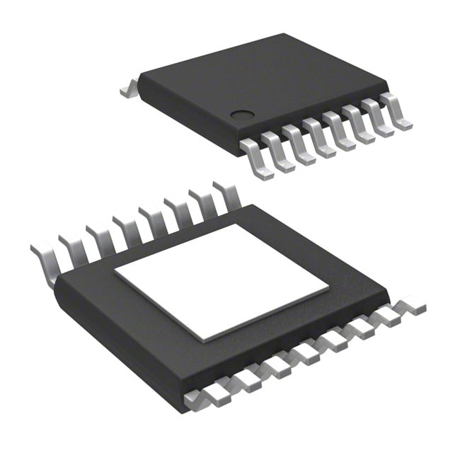
| 供应商器件封装 | 16-HTSSOP |
| 其它名称 | 296-34614-5 |
| 包装 | 管件 |
| 同步整流器 | 是 |
| 商标 | Texas Instruments |
| 安装类型 | 表面贴装 |
| 安装风格 | SMD/SMT |
| 封装 | Tube |
| 封装/外壳 | 16-TSSOP (0.173", 4.40mm 宽)裸焊盘 |
| 封装/箱体 | HTSSOP-16 |
| 工作温度 | -40°C ~ 125°C |
| 工作温度范围 | - 40 C to + 145 C |
| 工厂包装数量 | 90 |
| 开关频率 | 300 kHz |
| 拓扑结构 | Buck |
| 最大工作温度 | + 145 C |
| 最大输入电压 | 18 V |
| 最小工作温度 | - 40 C |
| 最小输入电压 | 4.5 V |
| 标准包装 | 90 |
| 电压-输入 | 4.5 V ~ 18 V |
| 电压-输出 | 0.8 V ~ 16.2 V |
| 电流-输出 | 1.5A,2.5A |
| 类型 | 降压(降压) |
| 系列 | TPS54290 |
| 输入电压 | 4.5 V to 18 V |
| 输出数 | 2 |
| 输出电压 | 0.8 V to 16.2 V |
| 输出电流 | 1.5 A, 2.5 A |
| 输出端数量 | 2 Output |
| 输出类型 | 可调式 |
| 频率-开关 | 300kHz |


- 商务部:美国ITC正式对集成电路等产品启动337调查
- 曝三星4nm工艺存在良率问题 高通将骁龙8 Gen1或转产台积电
- 太阳诱电将投资9.5亿元在常州建新厂生产MLCC 预计2023年完工
- 英特尔发布欧洲新工厂建设计划 深化IDM 2.0 战略
- 台积电先进制程称霸业界 有大客户加持明年业绩稳了
- 达到5530亿美元!SIA预计今年全球半导体销售额将创下新高
- 英特尔拟将自动驾驶子公司Mobileye上市 估值或超500亿美元
- 三星加码芯片和SET,合并消费电子和移动部门,撤换高东真等 CEO
- 三星电子宣布重大人事变动 还合并消费电子和移动部门
- 海关总署:前11个月进口集成电路产品价值2.52万亿元 增长14.8%


PDF Datasheet 数据手册内容提取
Product Sample & Technical Tools & Support & Folder Buy Documents Software Community TPS54290,TPS54291,TPS54292 SLUS973A–OCTOBER2009–REVISEDNOVEMBER2016 TPS5429x 1.5-A and 2.5-A Dual, Fully-Synchronous Buck Converter With Integrated MOSFET 1 Features 3 Description • 4.5-Vto18-VInputRange The TPS54290, TPS54291, and TPS54292 devices 1 are dual-output, fully synchronous buck converters • OutputVoltageRange0.8VtoD ×V MAX IN capable of supporting applications with a minimal • FullyIntegratedDualBuck:1.5Aand2.5A number of external components. It operates from a • ThreeFixedSwitchingFrequencyVersions: 4.5-V to 18-V input supply voltage, and supports output voltages as low as 0.8 V and as high as 90% – TPS54290:300kHz oftheinputvoltage. – TPS54291:600kHz Both high-side and low-side MOSFETs are integrated – TPS54292:1.2MHz to provide fully synchronous conversion with higher • IntegratedUVLO efficiency. Channel 1 can provide up to 1.5 A of • 0.8V With1%Accuracy(0°Cto85°C) continuous current. Meanwhile, Channel 2 supports REF upto2.5A. • InternalSoftStart: – TPS54290:5.2ms Current mode control simplifies the compensation. The external compensation adds flexibility for the – TPS54291:2.6ms usertochoosedifferenttypeofoutputcapacitors. – TPS54292:1.3ms 180° out-of-phase operation reduces the ripple • DualPWMOutputs180° Out-of-Phase current through the input capacitor, providing the • DedicatedEnableforEachChannel benefit of reducing input capacitance, alleviating EMI • CurrentModeControlforSimplified andincreasingcapacitorlife. Compensation DeviceInformation(1) • ExternalCompensation PARTNUMBER PACKAGE BODYSIZE(NOM) • Pulse-by-PulseOvercurrentProtection, TPS54290 2.2-Aand3.8-AOvercurrentLimit TPS54291 HTSSOP(16) 5.00mm×4.40mm • IntegratedBootstrapSwitch TPS54292 • ThermalShutdownProtectionat145°C (1) For all available packages, see the orderable addendum at theendofthedatasheet. • 16-Pin PowerPAD™HTSSOPPackage 2 Applications • Set-TopBoxes • DigitalTVs • PowerforDSP • ConsumerElectronics SimplifiedSchematic V IN TPS54290 1 PVDD1 PVDD2 16 2 BOOT1 BOOT2 15 V V OUT1 OUT2 3 SW1 SW2 14 4 PGND1 PGND2 13 5 EN1 BP 12 6 EN2 GND 11 7 FB1 FB2 10 8 COMP1 COMP2 9 GND UDG-09130 Copyright © 2016,Texas Instruments Incorporated 1 An IMPORTANT NOTICE at the end of this data sheet addresses availability, warranty, changes, use in safety-critical applications, intellectualpropertymattersandotherimportantdisclaimers.PRODUCTIONDATA.
TPS54290,TPS54291,TPS54292 SLUS973A–OCTOBER2009–REVISEDNOVEMBER2016 www.ti.com Table of Contents 1 Features.................................................................. 1 9.1 ApplicationInformation ..........................................18 2 Applications........................................................... 1 9.2 TypicalApplications................................................18 3 Description............................................................. 1 10 PowerSupplyRecommendations..................... 25 4 RevisionHistory..................................................... 2 11 Layout................................................................... 25 5 DeviceComparisonTable..................................... 3 11.1 LayoutGuidelines.................................................25 11.2 LayoutExamples...................................................26 6 PinConfigurationandFunctions......................... 3 11.3 OvertemperatureProtectionandJunction 7 Specifications......................................................... 5 TemperatureRise....................................................27 7.1 AbsoluteMaximumRatings......................................5 11.4 PowerDerating.....................................................28 7.2 ESDRatings..............................................................5 12 DeviceandDocumentationSupport................. 29 7.3 RecommendedOperatingConditions.......................5 12.1 DocumentationSupport........................................29 7.4 ThermalInformation..................................................5 12.2 RelatedLinks........................................................29 7.5 ElectricalCharacteristics...........................................6 12.3 ReceivingNotificationofDocumentationUpdates29 7.6 TypicalCharacteristics..............................................8 12.4 CommunityResources..........................................29 8 DetailedDescription............................................ 10 12.5 Trademarks...........................................................29 8.1 Overview.................................................................10 12.6 ElectrostaticDischargeCaution............................29 8.2 FunctionalBlockDiagram.......................................10 12.7 Glossary................................................................29 8.3 FeatureDescription.................................................11 13 Mechanical,Packaging,andOrderable 8.4 DeviceFunctionalModes........................................17 Information........................................................... 30 9 ApplicationandImplementation........................ 18 4 Revision History NOTE:Pagenumbersforpreviousrevisionsmaydifferfrompagenumbersinthecurrentversion. ChangesfromOriginal(October2009)toRevisionA Page • AddedESDRatingstable,ThermalInformationtable,FeatureDescriptionsection,DeviceFunctionalModes, ApplicationandImplementationsection,PowerSupplyRecommendationssection,Layoutsection,Deviceand DocumentationSupportsection,andMechanical,Packaging,andOrderableInformationsection....................................... 1 • DeletedOrderingInformationtable;seePOAattheendofthedatasheet........................................................................... 1 • DeletedLeadtemperature(260°Cmaximum)........................................................................................................................ 5 • AddedThermalInformationtabletoreplacethePackageDissipationRatingstable............................................................ 5 2 SubmitDocumentationFeedback Copyright©2009–2016,TexasInstrumentsIncorporated ProductFolderLinks:TPS54290 TPS54291 TPS54292
TPS54290,TPS54291,TPS54292 www.ti.com SLUS973A–OCTOBER2009–REVISEDNOVEMBER2016 5 Device Comparison Table DEVICE DESCRIPTION TPS40222 5-VInput,1.5-A,Non-SynchronousBuckConverter TPS5428x 2-ADualNon-SynchronousConverterwithIntegratedHigh-SideFET TPS5538x 3-ADualNon-SynchronousConverterwithIntegratedHigh-SideFET 6 Pin Configuration and Functions PWPPackage 16-PinHTSSOP TopView PVDD1 1 16 PVDD2 BOOT1 2 15 BOOT2 SW1 3 14 SW2 PGND1 4 13 PGND2 Thermal Pad EN1 5 12 BP EN2 6 11 GND FB1 7 10 FB2 COMP1 8 9 COMP2 Not to scale PinFunctions PIN I/O DESCRIPTION NO. NAME PowerinputtotheOutput1high-sideMOSFETonly.Thispinmustbelocallybypassedto 1 PVDD1 I PGND1withalow-ESRceramiccapacitorof10µForgreater.PVDD1andPVDD2couldbe tiedexternallytogether. Inputsupplytothehigh-sidegatedriverforOutput1.Connecta22-nFto68-nFcapacitorfrom thispintoSW1.ThiscapacitorischargedfromtheBPpinvoltagethroughaninternalswitch. 2 BOOT1 I TheswitchisturnedONduringtheoff-timeoftheconverter.ToslowdowntheturnONofthe internalFET,asmallresistor(2Ωto5Ω)maybeplacedinserieswiththebootstrap capacitor. 3 SW1 O Source(switching)outputforOutput1PWM PowergroundforOutputx.ItisseparatedfromGNDtopreventtheswitchingnoisecoupledto 4 PGND1 — theinternallogiccircuits. Active-lowenableinputforOutput1.Ifthevoltageonthispinisgreaterthan1.5V,Output1is disabled(high-sideswitchisOFF).Avoltageoflessthan0.9VenablesOutput1andallow 5 EN1 I softstartofOutput1tobegin.AninternalcurrentsourcedrivesthispintoPVDD2ifleft floating.ConnectthispintoGNDtobypasstheenablefunction. Active-lowenableinputforOutput2.Ifthevoltageonthispinisgreaterthan1.5V,Output2is disabled(high-sideswitchisOFF).Avoltageoflessthan0.9VenablesOutput2andallow 6 EN2 I softstartofOutput2tobegin.AninternalcurrentsourcedrivesthispintoPVDD2ifleft floating.ConnectthispintoGNDtobypasstheenablefunction. VoltagefeedbackpinforOutputx.Theinternaltransconductanceerroramplifieradjuststhe PWMforOutputxtoregulatethevoltageatthispintotheinternal0.8-Vreference.Aseries 7 FB1 I resistordividerfromOutputxtoground,withthecenterconnectiontiedtothispin,determines thevalueoftheregulatedoutputvoltage. Outputofthetransconductance(g )amplifier.AR-Ccompensationnetworkisconnected 8 COMP1 O M fromCOMPxtoGND. Copyright©2009–2016,TexasInstrumentsIncorporated SubmitDocumentationFeedback 3 ProductFolderLinks:TPS54290 TPS54291 TPS54292
TPS54290,TPS54291,TPS54292 SLUS973A–OCTOBER2009–REVISEDNOVEMBER2016 www.ti.com PinFunctions(continued) PIN I/O DESCRIPTION NO. NAME Outputofthetransconductance(g )amplifier.AR-Ccompensationnetworkisconnected 9 COMP2 O M fromCOMPxtoGND. VoltagefeedbackpinforOutputx.Theinternaltransconductanceerroramplifieradjuststhe PWMforOutputxtoregulatethevoltageatthispintotheinternal0.8-Vreference.Aseries 10 FB2 I resistordividerfromOutputxtoground,withthecenterconnectiontiedtothispin,determines thevalueoftheregulatedoutputvoltage. 11 GND — Analoggroundpinforthedevice. Regulatedvoltagetochargethebootstrapcapacitors.BypassthispintoGNDwithalow-ESR, 12 BP — 4.7-µFceramiccapacitor(10-µFcapacitorpreferred). PowergroundforOutputx.ItisseparatedfromGNDtopreventtheswitchingnoisecoupledto 13 PGND2 — theinternallogiccircuits. 14 SW2 O Source(switching)outputforOutput2PWM. Inputsupplytothehigh-sidegatedriverforOutput2.Connecta22-nFto68-nFcapacitorfrom thispintoSW2.ThiscapacitorischargedfromtheBPpinvoltagethroughaninternalswitch. 15 BOOT2 I TheswitchisturnedONduringtheoff-timeoftheconverter.ToslowdowntheturnONofthe internalFET,asmallresistor(2Ωto5Ω)maybeplacedinserieswiththebootstrap capacitor. ThePVDD2pinprovidespowertothedevicecontrolcircuitry,providesthepullupfortheEN1 andEN2pinsandprovidespowertotheOutput2high-sideMOSFET.Thispinmustbelocally 16 PVDD2 I bypassedtoPGND2withalow-ESRceramiccapacitorof10µForgreater.TheUVLO functionmonitorsPVDD2andenablesthedevicewhenPVDD2isgreaterthan4.2V. — ThermalPad — Thispadmustbetiedexternallytoagroundplane. 4 SubmitDocumentationFeedback Copyright©2009–2016,TexasInstrumentsIncorporated ProductFolderLinks:TPS54290 TPS54291 TPS54292
TPS54290,TPS54291,TPS54292 www.ti.com SLUS973A–OCTOBER2009–REVISEDNOVEMBER2016 7 Specifications 7.1 Absolute Maximum Ratings overoperatingfree-airtemperaturerange(unlessotherwisenoted)(1) MIN MAX UNIT PVDD1,PVDD2,EN1,EN2 –0.3 20 V SW1,SW2 –1 20 V BOOT1,BOOT2 –0.3 SW+7 V SW1,SW2transient(<50ns) –3 20 V BP 7 V FB1,FB2 –0.3 3 V Operatingjunctiontemperature,T –40 145 °C J Storagetemperature,T –55 155 °C stg (1) StressesbeyondthoselistedunderAbsoluteMaximumRatingsmaycausepermanentdamagetothedevice.Thesearestressratings only,whichdonotimplyfunctionaloperationofthedeviceattheseoranyotherconditionsbeyondthoseindicatedunderRecommended OperatingConditions.Exposuretoabsolute-maximum-ratedconditionsforextendedperiodsmayaffectdevicereliability. 7.2 ESD Ratings VALUE UNIT Human-bodymodel(HBM),perANSI/ESDA/JEDECJS-001(1) ±2000 V Electrostaticdischarge V (ESD) Charged-devicemodel(CDM),perJEDECspecificationJESD22-C101(2) ±1500 (1) JEDECdocumentJEP155statesthat500-VHBMallowssafemanufacturingwithastandardESDcontrolprocess. (2) JEDECdocumentJEP157statesthat250-VCDMallowssafemanufacturingwithastandardESDcontrolprocess. 7.3 Recommended Operating Conditions overoperatingfree-airtemperaturerange(unlessotherwisenoted) MIN MAX UNIT V Inputvoltage 4.5 18 V DD T Junctiontemperature –40 125 °C J 7.4 Thermal Information TPS54290 TPS54291 THERMALMETRIC(1) TPS54292 UNIT PWP(HTSSOP) 16PINS R Junction-to-ambientthermalresistance 39.2 °C/W θJA R Junction-to-case(top)thermalresistance 27.7 °C/W θJC(top) R Junction-to-boardthermalresistance 22.3 °C/W θJB ψ Junction-to-topcharacterizationparameter 0.8 °C/W JT ψ Junction-to-boardcharacterizationparameter 22.1 °C/W JB R Junction-to-case(bottom)thermalresistance 2.7 °C/W θJC(bot) (1) Formoreinformationabouttraditionalandnewthermalmetrics,seetheSemiconductorandICPackageThermalMetricsapplication report. Copyright©2009–2016,TexasInstrumentsIncorporated SubmitDocumentationFeedback 5 ProductFolderLinks:TPS54290 TPS54291 TPS54292
TPS54290,TPS54291,TPS54292 SLUS973A–OCTOBER2009–REVISEDNOVEMBER2016 www.ti.com 7.5 Electrical Characteristics T =–40°Cto125°C,PVDD1andPVDD2=12V(unlessotherwisenoted) J PARAMETER TESTCONDITIONS MIN TYP MAX UNIT INPUTSUPPLY PVDD1,PVDD2 Inputvoltagerange 4.5 18 V IDD Shutdowncurrent EN1=EN2=PVDD2(4.5Vto18V) 80 160 µA SDN IDD Quiescent,non-switching FB1=FB2=1V,outputsoff 1.65 3 mA Q IDD Quiescent,whileswitching FB1=FB2=0.75V,measuredatBP 10 mA SW UVLO Minimumturnonvoltage PVDD2only 3.8 4.1 4.4 V UVLO Hysteresis 460 600 mV HYS t (1)(2) Timefromstart-uptosoftstart CBP=10µF,EN1andEN2golow 1.5 ms start begin simultaneously ENABLE(ACTIVELOW) Enablethresholdvoltage 0.9 1.2 1.5 V V ENx Hysteresis 70 mV I Enablepullupcurrent 10 µA ENx t (1) Timefromenabletosoftstart Otherenablepin=GND 10 µs ENx begin BPREGULATOR BP Regulatorvoltage 8V≤V ≤18V 5 5.2 5.6 V PVDD2 BP Dropoutvoltage V =4.5V 400 mV LDO PVDD2 I Regulatorshortcurrent 4.5V≤V ≤18V 25 mA BPS PVDD2 OSCILLATOR TPS54290 260 300 360 kHz f Oscillatorfrequency TPS54291 520 600 720 SW TPS54292 1040 1200 1440 kHz t (1) Clockdeadtime 140 ns DEAD g TRANSCONDUCTANCEAMPLIFIERANDVOLTAGEREFERENCE(APPLIESTOBOTHCHANNELS) M 0°C<T <85°C 792 800 808 mV J V Feedbackinputvoltage FB –40ºC<T <125°C 786 800 812 mV J I FeedbackInputbiascurrent V =0.8V 5 50 nA FB FB g (1) Transconductance 200 325 450 µS M Erroramplifiersourcecurrent I V =V =0.7V,V =0V 15 30 40 µA SOURCE capability FB1 FB2 COMP Erroramplifiersinkcurrent I V =V =0.9V,V =2V 15 30 40 µA SINK capability FB1 FB2 COMP SOFTSTART(APPLIESTOBOTHCHANNELS) TPS54290,0V≤V ≤0.8V 4 5.2 6 FB t Soft-starttime TPS54291 2 2.6 3 ms SS TPS54292 1 1.3 1.6 OVERCURRENTPROTECTION I CurrentlimitCH1 1.8 2.2 2.6 A CL1 I CurrentlimitCH2 3.2 3.8 4.6 A CL2 TPS54290 30 ms T (1) Hiccuptimeout TPS54291 16 HICCUP TPS54292 8 t (1) Minimumovercurrentpulse 150 200 ns ONOC (1) Specifiedbydesign.Nottestedinproduction. (2) Whenbothoutputsarestartedsimultaneously,a20-mAcurrentsourcechargestheBPcapacitor.Fastertimesarepossiblewithalower BPcapacitorvalue(seeInputUVLOandStart-Up) 6 SubmitDocumentationFeedback Copyright©2009–2016,TexasInstrumentsIncorporated ProductFolderLinks:TPS54290 TPS54291 TPS54292
TPS54290,TPS54291,TPS54292 www.ti.com SLUS973A–OCTOBER2009–REVISEDNOVEMBER2016 Electrical Characteristics (continued) T =–40°Cto125°C,PVDD1andPVDD2=12V(unlessotherwisenoted) J PARAMETER TESTCONDITIONS MIN TYP MAX UNIT BOOTSTRAP(APPLIEDTOBOTHCHANNELS) R Bootstrapswitchresistance R(BPtoBOOT),Iexternal=10mA 33 Ω BOOT PGOOD V FeedbackvoltagelimitforPGOOD 660 730 mV UV V (1) PGOODhysteresisvoltageonFB 40 mV PG-HYST OUTPUTSTAGE(APPLIEDTOBOTHCHANNELS) R (HS)(1) On-resistanceofhigh-sideFET 170 265 mΩ DS(on1) andbondwireonCH1 R (HS)(1) On-resistanceofhigh-sideFET 120 190 mΩ DS(on2) andbondwireonCH2 R (LS)(1) On-resistanceoflow-sideFETand 120 190 mΩ DS(on1) bondwireonCH1 R (LS)(1) On-resistanceoflow-sideFETand 90 150 mΩ DS(on2) bondwireonCH2 t (1) Minimumcontrollablepulsewidth 150 ns ON_MIN Minimumduty V =0.9V 0% cycle FB HDRVofftoLDRVon 20 ns t (1) Outputdriverdeadtime DEAD LDRVofftoHDRVon 20 ns TPS54290 90% 96% D Maximumdutycycle TPS54291 85% 91% MAX TPS54292 78% 82% THERMALSHUTDOWN T (1) Shutdowntemperature 145 °C SD T (1) Hysteresis 20 °C SD_HYS Copyright©2009–2016,TexasInstrumentsIncorporated SubmitDocumentationFeedback 7 ProductFolderLinks:TPS54290 TPS54291 TPS54292
TPS54290,TPS54291,TPS54292 SLUS973A–OCTOBER2009–REVISEDNOVEMBER2016 www.ti.com 7.6 Typical Characteristics 1.75 140 Non-Switching 120 –mA1.70 –Am 100 VIN=18V nt nt urre1.65 urre 80 C C ent wn VIN=12V Quiesc1.60 Shutdo 60 I–DDQ1.55 I–SD 40 VIN=4.5V 20 1.50 0 –40 –25 –10 5 20 35 50 65 80 95 110 125 –40 –25 –10 5 20 35 50 65 80 95 110 125 T –JunctionTemperature–°C T –JunctionTemperature–°C J J Figure1.QuiescentCurrentvsTemperature Figure2.ShutdownCurrentvsTemperature V 4.2 1.26 – e g a Volt 4.1 V1.24 d – hol UVLOON old1.22 es 4.0 sh Thr hre ervoltageLockout 33..89 UVLOOFF –EnableVoltageT111...211086 EnableOFF EnableON Und 3.7 VEN1.14 – O L V VU3.6 1.12 –40 –25 –10 5 20 35 50 65 80 95 110 125 –40 –25 –10 5 20 35 50 65 80 95 110 125 TJ–JunctionTemperature–°C TJ–JunctionTemperature–°C Figure3.UVLOTurnonandTurnoffThresholds Figure4.ENxTurnonandTurnoffThreshold vsTemperature vsTemperature 6 1.4 1.2 5 z H M me–ms 4 fSW=300kHz fSW=600kHz uency– 01..80 fSW=600kHz fSW=1.2MHz Ti eq art 3 Fr oft-St ching 0.6 –S 2 wit S S 0.4 S – t W S 1 f 0.2 fSW=1.2MHz fSW=300kHz 0 0 –40 –25 –10 5 20 35 50 65 80 95 110 125 –40 –25 –10 5 20 35 50 65 80 95 110 125 TJ–JunctionTemperature–°C TJ–JunctionTemperature–°C Figure5.Soft-StartTimevsTemperature Figure6.OscillatorFrequencyvsTemperature 8 SubmitDocumentationFeedback Copyright©2009–2016,TexasInstrumentsIncorporated ProductFolderLinks:TPS54290 TPS54291 TPS54292
TPS54290,TPS54291,TPS54292 www.ti.com SLUS973A–OCTOBER2009–REVISEDNOVEMBER2016 Typical Characteristics (continued) 808 4.50 Channel2 806 4.25 4.00 804 V –m 802 –A3.75 oltage 800 Limit3.50 edbackV 779968 –Current33..2050 –Fe 794 LIMx2.75 FB II Channel1 V 792 2.50 790 2.25 788 2.00 –40 –25 –10 5 20 35 50 65 80 95 110 125 –40 –25 –10 5 20 35 50 65 80 95 110 125 TJ–JunctionTemperature–°C TJ–JunctionTemperature–°C Figure7.FeedbackVoltagevsTemperature Figure8.CurrentLimitvsTemperature 5.20 9 8 A V m 7 –5.15 – oltage urrent 6 V C 5 n e o d ati5.10 No 4 ul h- g c Re wit 3 P S B – 2 –P5.05 off) VB SW( 1 I 0 V =12V VDD 5.00 -1 –40 –25 –10 5 20 35 50 65 80 95 110 125 –40 –25 –10 5 20 35 50 65 80 95 110 125 T –JunctionTemperature–°C T –JunctionTemperature–°C J J Figure9.BPVoltagevsTemperature Figure10.SWNodeLeakageCurrent vsTemperature Copyright©2009–2016,TexasInstrumentsIncorporated SubmitDocumentationFeedback 9 ProductFolderLinks:TPS54290 TPS54291 TPS54292
TPS54290,TPS54291,TPS54292 SLUS973A–OCTOBER2009–REVISEDNOVEMBER2016 www.ti.com 8 Detailed Description 8.1 Overview The TPS5429x is a dual-output fully synchronous buck converter. Each PWM channel contains an error amplifier, current mode pulse width modulator (PWM), switching and rectifying MOSFETs, enable, and fault protection circuitry. Common to the two channels are the internal voltage regulator, voltage reference, and clock oscillator. 8.2 Functional Block Diagram BP 2 BOOT1 f(I )+DC(ofst) DRAIN1 1 PVDD1 Current FET Comparator CLK1 Switch I DRAIN1 S Q + COMP1 8 R R Q 3 SW1 f(I ) DRAIN1 + FB1 7 BP 0.8V + OvercurrentComp REF f(ISLOPE1) f(IMAX1) CLK1 Anti-Cross SoftStart Conduction 4 PGND1 SD1 1 TSD 10mA 10mA (max) (max) EN1 5 SD1 f(I ) SLOPE1 Internal Ramp SD2 EN2 6 Control Gen1 UVLO 2.4MHz Divideby CLK1 Oscilator 2/4/8 f(I ) SLOPE2 FB1 Output Ramp Undervoltage Gen2 FB2 Detect CLK2 PVDD2 5.25-V BP 12 References Regulator BP 15 BOOT2 GND 11 f(I )+DC(ofst) DRAIN2 16 PVDD2 Current FET Comparator CLK2 Switch I DRAIN2 S Q + COMP2 9 R R Q 14 SW2 f(I ) DRAIN2 + FB2 10 BP 0.8V + OvercurrentComp REF f(ISLOPE2) f(IMAX2) CLK2 Anti-Cross SoftStart Conduction 13 PGND2 SD2 2 FET Switch UDG-09124 Copyright © 2016,Texas Instruments Incorporated 10 SubmitDocumentationFeedback Copyright©2009–2016,TexasInstrumentsIncorporated ProductFolderLinks:TPS54290 TPS54291 TPS54292
TPS54290,TPS54291,TPS54292 www.ti.com SLUS973A–OCTOBER2009–REVISEDNOVEMBER2016 8.3 Feature Description 8.3.1 VoltageReference The band-gap cell common to both outputs, trimmed to 800 mV. The reference voltage is 1% accurate in the temperaturerangefrom0°Cto85°C. 8.3.2 Oscillator The oscillator frequency is internally fixed at 2.4 MHz that is divided by 8/4/2 to generate the ramps for TPS5429x, respectively. The two outputs are internally configured to operate on alternating switch cycles (that is, 180° out-of-phase). 8.3.3 InputUVLOandStart-Up When the voltage at the PVDD2 pin is less than 4.4 V, a portion of the internal bias circuitry is operational, and all other functions are held OFF. All of the internal MOSFETs are also held OFF. When the PVDD2 voltage rises above the UVLO turnon threshold, the state of the enable pins determines the remainder of the internal start-up sequence. If either output is enabled (ENx pulled low), the BP regulator turns on, charging the BP capacitor with a20-mAcurrent.WhentheBPpinisgreaterthan4V,PWMisenabledandsoftstartcommences. NOTE The internal regulator and control circuitry are powered from PVDD2. The voltage on PVDD1maybehigherorlowerthanPVDD2. 8.3.4 EnableandTimedTurnonoftheOutputs Each output has a dedicated (active low) enable pin. If left floating, an internal current source pulls the pin to PVDD2. By grounding, or by pulling the ENx pin to below approximately 1.25 V with an external circuit, the associatedoutputisenabledandsoftstartisinitiated. If both enable pins are left in the high state, the device operates in a shutdown mode, where the BP regulator shuts down and minimal house keeping functions are active. The total standby current from both PVDD pins is 80µAat12-Vinputsupply. An R-C connect to an ENx pin may be used to delay the turnon of the associated output after power is applied to PVDDx (see Figure 11). After power is applied to PVDD2, the voltage on the ENx pin slowly decays towards ground. Once the voltage decays to approximately 1.25 V, then the output is enabled and the start-up sequence begins. If it is desired to enable the outputs of the device immediately upon the application of power to the PVDD2pin,thenomitthesetwocomponentsandtiethe ENxpintoGNDdirectly. If an R-C circuit is used to delay the turnon of the output, the resistor value must be an order of magnitude less than 1.25 V / 10 µA or 120 kΩ. A suggested value is 51 kΩ. This allows the ENx voltage to decay below the 1.25-Vthresholdwhilethe10-µAbiascurrentflows. Thetimetostart(aftertheapplicationofPVDD2)isEquation1. tSTART =-R´C´lnæççèV(VINTH-2-´IEIENuuNxuuuxr)´´RRö÷÷ø (s) where • RandCarethetimingcomponents • V isthe1.25-Venablethresholdvoltage TH • I isthe10-µAmaximumenablepinbiasingcurrent (1) EN Figure11andFigure12illustratestartupdelaywithanR-Cfilterontheenablepin(s). Copyright©2009–2016,TexasInstrumentsIncorporated SubmitDocumentationFeedback 11 ProductFolderLinks:TPS54290 TPS54291 TPS54292
TPS54290,TPS54291,TPS54292 SLUS973A–OCTOBER2009–REVISEDNOVEMBER2016 www.ti.com Feature Description (continued) PVDD2 10mA(max) C ENx PVDDx + PVDDx 1.25V 1.25-V R Threshold TPS5429x UDG-09125 ENxB Copyright © 2016,Texas Instruments Incorporated V OUTx Time 0 t t +t DELAY DELAY SS Figure11.Start-UpDelaySchematic Figure12.Start-UpDelayTimingDiagram NOTE If delayed output voltage start-up is not necessary, simply connect EN1 and EN2 to GND. Thisallowstheoutputsto startimmediatelyonthevalidapplicationofPVDD2. If ENx is allowed to go high after the Outputx has been in regulation, the upper and lower MOSFETs shut off, and the output decays at a rate determined by the output capacitor andtheload. 8.3.5 SoftStart Each output has a dedicated soft-start circuit. The soft-start voltage is an internal digital reference ramp to one of the two noninverting inputs of the error amplifier. The other input is the internal precise 0.8-V reference. The total ramp time for the FB voltage to charge from 0 V to 0.8 V is about 5.2 ms, 2.6 ms, and 1.3 ms for TPS54190, TPS54191, and TPS54192, respectively. During a soft-start interval, the TPS5429x output slowly increases the voltage to the noninverting input of the error amplifier. In this way, the output voltage slowly ramps up until the voltage on the noninverting input to the error amplifier reaches the internal 0.8-V reference voltage. At that time, thevoltageatthenoninvertinginputtotheerroramplifierremainsatthereferencevoltage. During the soft-start interval, pulse-by-pulse current limiting is in effect. If an overcurrent pulse is detected, six PWM pulses is skipped to allow the inductor current to decay before another PWM pulse is applied (see Output OverloadProtection).Thereisnopulseskippingifacurrentlimitpulseisnotdetected. If the rate of rise of the input voltage (PVDDx) is such that the input voltage is too low to support the desired regulation voltage by the time soft start completes, the output UV circuit may trip and cause a hiccup in the output voltage. In this case, use a timed delay start-up from the ENx pin to delay the start-up of the output until thePVDDxvoltagehasthecapabilityofsupportingthedesiredregulationvoltage. 8.3.6 OutputVoltageRegulation The regulation output voltage is determined by a resistor divider connecting the output node, the FBx pin, and GND(Figure13).ThevalueoftheoutputvoltageisshowninEquation2. æ R1ö VOUT = VREF´ç1+R2÷ (V) è ø where • V istheinternal0.8-Vreferencevoltage (2) REF 12 SubmitDocumentationFeedback Copyright©2009–2016,TexasInstrumentsIncorporated ProductFolderLinks:TPS54290 TPS54291 TPS54292
TPS54290,TPS54291,TPS54292 www.ti.com SLUS973A–OCTOBER2009–REVISEDNOVEMBER2016 Feature Description (continued) TPS54290 1 PVDD1 PVDD2 16 2 BOOT1 BOOT2 15 V OUT1 3 SW1 SW2 14 4 PGND1 PGND2 13 R1 5 EN1 BP 12 6 EN2 GND 11 7 FB1 FB2 10 8 COMP1 COMP2 9 R2 UDG-09131 Copyright © 2016,Texas Instruments Incorporated Figure13. FeedbackNetworkforChannel1 8.3.7 InductorSelection Equation 3 calculates the inductance value so that the output ripple current falls from 20% to 40% of the full load current. V -V L= IN OUT DI OUT (3) 8.3.8 MaximumOutputCapacitance With internal pulse-by-pulse current limiting and a fixed soft-start time, there is a maximum output capacitance whichmaybeusedbeforestart-upproblemsbegintooccur.Iftheoutputcapacitanceislargeenoughsothatthe device enters a current-limit protection mode during start-up, then there is a possibility that the output never reaches regulation. Instead, the TPS5429x simply shuts down and attempts a restart as if the output were short- circuited to ground. The maximum output capacitance (including bypass capacitance distributed at the load) is givenbyEquation4. t æ æI öö COUT(max) = SS ´çILIM-ILOAD -ç RIPPLE ÷÷ VOUT è è 2 øø where • t isthesoft-starttime SS • ILIMisthecurrentlimitlevel (4) 8.3.9 FeedbackLoopCompensation In the feedback signal path, the output voltage setting divider is followed by an internal g -type error amplifier M with a typical transconductance of 325 µS. An external series connected R-C circuit from the g amplifier output M (COMPxpin)togroundservesasthecompensationnetworkfortheconverter.Thesignalfromtheerroramplifier output is then buffered and combined with a slope compensation signal before it is mirrored to be referenced to the SW node. Here, it is compared with the current feedback signal to create a pulse-width-modulated (PWM) signal-fed to drive the upper MOSFET switch. A simplified equivalent circuit of the signal control path is depicted inFigure14. Copyright©2009–2016,TexasInstrumentsIncorporated SubmitDocumentationFeedback 13 ProductFolderLinks:TPS54290 TPS54291 TPS54292
TPS54290,TPS54291,TPS54292 SLUS973A–OCTOBER2009–REVISEDNOVEMBER2016 www.ti.com Feature Description (continued) NOTE NoisecouplingfromtheSWxnodetointernalcircuitryofBOOTxmayimpactnarrowpulse widthoperation,especiallyatloadcurrentslessthan1A. BP I –I COMP SLOPE Error x2 PWMto I Switch Amplifier SLOPE FB + I + COMP Offset f(I ) 0.8V DRAIN REF COMP GND 11.5kW R COMP C COMP UDG-09128 Figure14. FeedbackLoopEquivalentCircuit A more conventional small-signal equivalent block diagram is shown in Figure 15. Here, the full closed-loop signal path is shown. Because the TPS5429x contains internal slope compensation, the external L-C filter must beselectedappropriatelysothattheresultingcontrolloopmeetscriteriaforstability. V IN V V + C + OUT V Modulator REF _ _ Filter Current Feedback Network Compensation Network Figure15. SmallSignalEquivalentBlockDiagram To determine the components necessary for compensating the feedback loop, the controller frequency response characteristics must be understood and the desired crossover frequency selected. The best results are obtained if 10% of the switching frequency is used as this closed-loop crossover frequency. In some cases, up to 20% of theswitchingfrequencyisalsopossible. 14 SubmitDocumentationFeedback Copyright©2009–2016,TexasInstrumentsIncorporated ProductFolderLinks:TPS54290 TPS54291 TPS54292
TPS54290,TPS54291,TPS54292 www.ti.com SLUS973A–OCTOBER2009–REVISEDNOVEMBER2016 Feature Description (continued) With the output filter components selected, the next step is to calculate the DC gain of the modulator. For TPS5429x,useEquation5. f FM TPS5429x= SW æç19.7´e(K´tON)+95´10-6´æç(VIN -VOUT)ö÷ö÷ ç ç L ÷÷ è è øø where • K=5.6×10⁵forTPS54290 • K=1.5×10⁶forTPS54291 • K=3.6×10⁶forTPS54292 (5) TheoverallDCgainoftheconvertercontrol-to-outputtransferfunctionisapproximatedbyEquation6. fC = VIN´FM´2´10-4 æç æç(VIN´FM´95´10-6)ö÷ö÷ 1+ çç çç 2´RLOAD ÷÷÷÷ è è øø (6) The next step is to find the desired gain of the error amplifier at the desired crossover frequency. Assuming a single-poleroll-off,useEquation6toevaluateEquation7atthedesiredcrossoverfrequency. æ ö f K =-20´logç C ÷ EA ç(1+2´p´f ´(2´R )´C )÷ è CO LOAD OUT ø where • ƒ isthedesiredcrossoverfrequency (7) CO TPS54290 1 PVDD1 PVDD2 16 2 BOOT1 BOOT2 15 V Z OUT1 UPPER 3 SW1 SW2 14 4 PGND1 PGND2 13 C1 R1 5 EN1 BP 12 (Optional) 6 EN2 GND 11 7 FB1 FB2 10 8 COMP1 COMP2 9 C2 R2 R COMP (Optional) C COMP Z LOWER UDG-09129 Copyright © 2016,Texas Instruments Incorporated Figure16. LoopCompensationNetwork Copyright©2009–2016,TexasInstrumentsIncorporated SubmitDocumentationFeedback 15 ProductFolderLinks:TPS54290 TPS54291 TPS54292
TPS54290,TPS54291,TPS54292 SLUS973A–OCTOBER2009–REVISEDNOVEMBER2016 www.ti.com Feature Description (continued) If operating at wide duty cycles (over 50%), a capacitor may be necessary across the upper resistor of the voltagesettingdivider(seeEquation8).Ifdutycyclesarelessthan50%,thiscapacitormaybeomitted. L´C C1= OUT R1 (8) If a high-ESR capacitor is used in the output filter, a zero appears in the loop response that could lead to instability (see Equation 9). To compensate, a small capacitor is placed in parallel with the lower voltage setting divider resistor. The value of the capacitor is determined such that a pole is placed at the same frequency as the ESRzero.Iflow-ESRcapacitorsareused,thiscapacitormaybeomitted. ESR´(R1+R2) C2=COUT´ (R1´R2) (9) Next, calculate the value of the error amplifier gain setting resistor and capacitor using Equation 10 and Equation11. KEA 10 20 ´(Z +Z ) LOWER UPPER R = COMP g ´Z M LOWER (10) 1 C = COMP 2´p´f ´R POLE COMP where 1 • fPOLE = 2´p´(2´RLOAD)´COUT (11) NOTE When the filter and compensation component values have been established, laboratory measurementsofthephysicaldesignmustbeperformedtoconfirmconverterstability. 8.3.10 BootstrapforN-ChannelMOSFET A bootstrap circuit provides a voltage source higher than the input voltage and of sufficient energy to fully enhance the switching MOSFET each switching cycle. The PWM duty cycle is limited to maximum (that is, 90% for TPS54291) allowing an external bootstrap capacitor to charge through an internal synchronous switch (between BP and BOOTx) during every cycle. When the PWM switch is commanded to turn on, the energy used todrivetheMOSFETgateisderivedfromthevoltageonthiscapacitor. Because this is a charge transfer circuit, take care in selecting the value of the bootstrap capacitor. It must be sized such that the energy stored in the capacitor on a per cycle basis is greater than the gate charge requirement of the MOSFET being used. Typically a ceramic capacitor with a value from 22 nF to 68 nF is selectedforthebootstrapcapacitor. 8.3.11 OutputOverloadProtection In the event of an overcurrent on either output after the output reaches regulation, pulse-by-pulse current limit is in effect for that output. In addition, an output undervoltage (UV) comparator monitors the FBx voltage (which follows the output voltage) to declare a fault if the output drops below 85% of regulation. During this fault condition, both PWM outputs are disabled. This ensures that both outputs discharge to GND, in the event that overcurrent is on one output while the other is not loaded. The converter enters a hiccup mode timeout before attemptingtorestart. If an overcurrent condition exists during soft start, pulse-by-pulse current limiting reduces the pulse width of the affected output’s PWM. In addition, if an overcurrent pulse is detected, six clock cycles are skipped before a next PWM pulse is enabled, effectively dividing the PWM frequency by six and preventing excessive current build up in the inductor. At the end of the soft-start time, a UV fault is declared and the operation is the same as describedabove. 16 SubmitDocumentationFeedback Copyright©2009–2016,TexasInstrumentsIncorporated ProductFolderLinks:TPS54290 TPS54291 TPS54292
TPS54290,TPS54291,TPS54292 www.ti.com SLUS973A–OCTOBER2009–REVISEDNOVEMBER2016 Feature Description (continued) TheovercurrentthresholdforOutput1andOutput2aresetnominally2.2Aand3.8A,respectively. NOTE Design hint: The OCP Threshold refers to the peak current in the internal switch. Be sure to add the 1/2 of the peak inductor ripple current to the DC load current in determining howclosetheactualoperatingpointistotheOCPThreshold. 8.3.12 OperatingNearMaximumDutyCycle If the TPS5429x is operated at maximum duty cycle, and if the input voltage is insufficient to support the output voltage (at full load or during a load current transient) then there is a possibility that the output voltage falls from regulation and trip the output UV comparator. If this must occur, the TPS5429x protection circuitry declares a faultandentershiccupmode. NOTE Design hint: Ensure that under ALL conditions of line and load regulation that there is sufficientdutycycletomaintainoutputvoltageregulation. 8.3.13 Dual-SupplyOperation It is possible to operate a TPS5429x from two supply voltages. If this application is desired, then the sequencing of the supplies must be such that PVDD2 is above the UVLO voltage before PVDD1 begins to rise. This is to ensure the internal regulator and the control circuitry is in operation before PVDD1 supplies energy to the output. In addition, Output1 must be held in the disabled state (EN1 high) until there is sufficient voltage on PVDD1 to supportOutput1inregulation(seeOperatingNearMaximumDutyCycle). Thepreferredsequenceofeventsfollows: 1. PVDD2risesabovetheinputUVLOvoltage 2. PVDD1riseswithOutput1disableduntilPVDD1risesaboveleveltosupportOutput1regulation Withthetwoconditionsabovesatisfied,thereisnorestrictiononPVDD2tobegreaterthan,orlessthanPVDD1. NOTE Design hint: An R-C delay on EN1 may be used to delay the start-up of Output1 for a long enoughperiodoftimetoensurePVDD1cansupportOutput1load. 8.3.14 BypassingandFiltering As with any integrated circuit, supply bypassing is important for jitter-free operation. To improve the noise immunityoftheconverter,ceramicbypasscapacitorsmustbeplacedasclosetothepackageaspossible. • PVDD1toGND:Usea10-µFceramiccapacitor • PVDD2toGND:Usea10-µFceramiccapacitor • BPtoGND:Usea4.7-µFceramiccapacitor 8.4 Device Functional Modes 8.4.1 PWMOperation TPS5429X is a dual-channel synchronous buck converter. Normal operation occurs when V is above 4.5 V and IN theEN1andEN2pinspulledlowtoenablethedevice. 8.4.2 StandbyOperation TPS5429XcanbeplacedinstandbywhentheEN1andEN2pinsaresethigh,disablingthedevice. Copyright©2009–2016,TexasInstrumentsIncorporated SubmitDocumentationFeedback 17 ProductFolderLinks:TPS54290 TPS54291 TPS54292
TPS54290,TPS54291,TPS54292 SLUS973A–OCTOBER2009–REVISEDNOVEMBER2016 www.ti.com 9 Application and Implementation NOTE Information in the following applications sections is not part of the TI component specification, and TI does not warrant its accuracy or completeness. TI’s customers are responsible for determining suitability of components for their purposes. Customers should validateandtesttheirdesignimplementationtoconfirmsystemfunctionality. 9.1 Application Information TPS5429X is a synchronous buck converter. It can convert an input voltage of 4.5 V to 18 V to two lower voltages.Channel1isratedfor1.5-Aoutput,whileChannel2isratedfor2.5-Aoutput. 9.2 Typical Applications 9.2.1 TPS54291DesignExample The following example illustrates the design process and component selection for a 12-V to 5-V or 3.3-V dual non-synchronousbuckregulatorusingtheTPS54291converter. Copyright © 2016,Texas Instruments Incorporated Figure17. TPS54291DesignExample1Schematic 9.2.1.1 DesignRequirements A definition of symbols used can be found in Table 1. The efficiency, line regulation, and load regulation from printed-circuitboardsbuiltusingthisdesignareshowninFigure19andFigure20. Table1.DesignExampleElectricalCharacteristics PARAMETER TESTCONDITIONS MIN TYP MAX UNIT INPUTCHARACTERISTICS V Inputvoltage 8 12 14 V IN I Inputcurrent V =nom,I =max A IN IN OUT Noloadinputcurrent V =nom,I =0A 12 20 mA IN OUT V InputUVLO I =mintomax 4 4.2 4.4 V IN(UVLO) OUT 18 SubmitDocumentationFeedback Copyright©2009–2016,TexasInstrumentsIncorporated ProductFolderLinks:TPS54290 TPS54291 TPS54292
TPS54290,TPS54291,TPS54292 www.ti.com SLUS973A–OCTOBER2009–REVISEDNOVEMBER2016 Typical Applications (continued) Table1.DesignExampleElectricalCharacteristics(continued) PARAMETER TESTCONDITIONS MIN TYP MAX UNIT OUTPUTCHARACTERISTICS V Outputvoltage1 V =nom,I =nom 3.2 3.3 3.4 V OUT1 IN OUT V Outputvoltage2 V =nom,I =nom 1.15 1.2 1.25 V OUT2 IN OUT Lineregulation VIN=mintomax 1% Loadregulation I =mintomax 1% OUT V Output1voltageripple V =nom,I =max 50 mV OUT1(ripple) IN OUT1 PP V Output2voltageripple V =nom,I =max 24 mV OUT2(ripple) IN OUT2 PP I Outputcurrent1 V =mintomax 0 1.5 A OUT1 IN I Outputcurrent2 V =mintomax 0 2.5 A OUT2 IN I OutputovercurrentChannel1 V =nom,V =(V –5%) 1.8 2.2 2.6 A OCP1 IN OUT OUT1 I OutputovercurrentChannel2 V =nom,V =(V –5%) 3.2 3.8 4.6 A OCP2 IN OUT OUT2 TRANSIENTRESPONSE ΔV Changefromloadtransient ΔI =1Aat3µA/s 200 mV OUT OUT Settlingtime to1%ofV 1 ms OUT SYSTEMSCHARACTERISTICS f Switchingfrequency 500 600 700 kHz SW η Peakefficiency V =nom 90% PEAK IN η Fullloadefficiency V =nom,I =max 80% IN OUT T Operatingtemperature V =mintomax,I =mintomax 0 25 60 °C OP IN OUT 9.2.1.2 DetailedDesignProcedure ThelistofmaterialsforthisapplicationisshownbelowinTable2. Table2.DesignExampleListofMaterials REFERENCE QTY VALUE DESCRIPTION SIZE PARTNUMBER MFR DESIGNATOR C12 1 4.7µF Capacitor,Ceramic,10V,X5R,20% 0805 Std Std C2,C14 2 22µF Capacitor,Ceramic,6.3V,X5R,20% 1206 C3216X5R0J226M TDK C3,C13 2 470pF Capacitor,Ceramic,25V,X7R,20% 0603 Std Std C4,C11 2 0.047µF Capacitor,Ceramic,25V,X7R,20% 0603 Std Std C5,C10 2 10µF Capacitor,Ceramic,25V,X5R,20% 1210 C3225X5R1E106M TDK C6 2 1.8nF Capacitor,Ceramic,25V,X7R,20% 0603 Std Std C7 1 15pF Capacitor,Ceramic,25V,X7R,20% 0603 Std Std C8 1 47pF Capacitor,Ceramic,25V,X7R,20% 0603 Std Std C9 1 1.2nF Capacitor,Ceramic,25V,X7R,20% 0603 Std Std 0.402×0.394 L1 1 8.2µH Inductor,SMT,4.38A,20mΩ MSS1048-822L Coilcraft inch 0.402×0.394 L2 1 3.3µH Inductor,SMT,5.04A,10mΩ MSS1048-332L Coilcraft inch R10 1 40.2kΩ Resistor,Chip,1/16W,1% 0603 Std Std R2,R11 2 10Ω Resistor,Chip,1/16W,5% 0603 Std Std R3,R12 2 20.5kΩ Resistor,Chip,1/16W,1% 0603 Std Std R4 1 6.49kΩ Resistor,Chip,1/16W,1% 0603 Std Std R6 1 7.87kΩ Resistor,Chip,1/16W,1% 0603 Std Std R7 1 4.64kΩ Resistor,Chip,1/16W,1% 0603 Std Std 2.5A/1.5A, DualOutputFullySynchronousBuck U1 1 CSP TPS54291PWP TI 600Hz Converterw/IntegratedFET Copyright©2009–2016,TexasInstrumentsIncorporated SubmitDocumentationFeedback 19 ProductFolderLinks:TPS54290 TPS54291 TPS54292
TPS54290,TPS54291,TPS54292 SLUS973A–OCTOBER2009–REVISEDNOVEMBER2016 www.ti.com 9.2.1.2.1 DutyCycleEstimation ThedutycycleofthemainswitchingFETisestimatedbyEquation12andEquation13. V 3.3 V 1.2 DMAX1 » V OUT = 8.0 =0.413¾¾®DMAX2 » V OUT = 8.0 =0.15 IN(min) IN(min) (12) V 3.3 V 1.2 DMIN1» OUT = =0.236¾¾®DMIN2 » OUT = =0.086 V 14 V 14 IN(max) IN(max) (13) 9.2.1.2.2 InductorSelection The peak-to-peak ripple must be limited to between 20% and 30% of the maximum output current (see Equation14andEquation15). I =0.30´I =0.3´1.5A =0.450A Lrip1(max) OUT(max) (14) I =0.30´I =0.3´2.5A =0.750A Lrip2(max) OUT(max) (15) TheminimuminductorsizecanbeestimatedbyEquation16andEquation17. VIN(max)-VOUT 1 14-3.3 1 LMIN1» ´DMIN´ = ´0.236´ =9.35mH I f 0.45A 600kHz LRIP(max) SW (16) VIN(max)-VOUT 1 14-1.2 1 LMIN2 » I ´DMIN´f = 0.75A ´0.086´ 600kHz = 2.45mH LRIP(max) SW (17) The standard inductor values of 8.2 µH and 3.3 µH are selected for Channel 1 and Channel 2, respectively. The actualripplecurrentsareestimatedbyEquation18andEquation19. VIN(max)-VOUT 1 14-3.3 1 IRIPPLE1» ´DMIN´ = ´0.236´ =0.513A L1 fSW 8.2mH 600kHz (18) VIN(max)-VOUT 1 14-1.2 1 IRIPPLE2 » ´DMIN´ = ´0.086´ =0.556A L2 fSW 3.3mH 600kHz (19) TheRMScurrentthroughtheinductorisapproximatedbyEquation20andEquation21. I = I 2 + 1 I 2 » I 2 + 1 I 2 = (1.5)2 + 1 (0.513)2A =1.51A L(rms) L(avg) 12RIPPLE OUT(max) 12RIPPLE 12 (20) I = I 2 + 1 I 2 » I 2 + 1 I 2 = (2.5)2 + 1 (0.556)2A =2.51A L(rms) L(avg) 12RIPPLE OUT(max) 12RIPPLE 12 (21) ADCcurrentwith30%peak-to-peakripplehasanRMScurrentapproximately0.4%abovetheaveragecurrent. ThepeakinductorcurrentisestimatedbyEquation22andEquation23. I »I + 1 I =1.5A+ 1 0.513A =1.76A L(peak) OUT(max) 2 RIPPLE 2 (22) I »I + 1 I =2.5A+ 1 0.556A =2.78A L(peak) OUT(max) 2 RIPPLE 2 (23) A 8.2-µH inductor with a minimum RMS current rating of 1.51 A and minimum saturation current rating of 3.7 A must be selected. A Coilcraft MSS1048-822ML 8.2-µH, 4.38-A inductor is chosen for Channel 1 and a Coilcraft MSS1048-3323.3-µHinductorischosenforChannel2. 20 SubmitDocumentationFeedback Copyright©2009–2016,TexasInstrumentsIncorporated ProductFolderLinks:TPS54290 TPS54291 TPS54292
TPS54290,TPS54291,TPS54292 www.ti.com SLUS973A–OCTOBER2009–REVISEDNOVEMBER2016 9.2.1.2.3 OutputCapacitorSelection Output capacitors are selected to support load transients and output ripple current. The minimum output capacitancetomeetthetransientspecificationisgivenbyEquation24andEquation25. ITRAN(max)2´L 1A2´8.2mH C = = =12.4mF OUT1(min) (VOUT)´VOVER 3.3V´0.2V (24) ITRAN(max)2´L 1A2´3.3mH C = = =13.7mF OUT2(min) (VOUT)´VOVER 1.2V´0.2V (25) ThemaximumESRtomeettheripplespecificationisgivenbyEquation26andEquation27. æ I ö æ 0.513A ö VRIPPLE(total) -çè8´CROIPUPTL´EfSW ÷ø 0.050V-çè8´12.4mF´600kHzø÷ ESR = = =0.081W MAX I 0.513A RIPPLE (26) æ I ö æ 0.556A ö VRIPPLE(total) -çè8´CROIPUPTL´EfSW ÷ø 0.024V-èç8´13.7mF´600kHz÷ø ESR = = =0.028W MAX I 0.556A RIPPLE (27) A single 22-µF ceramic capacitor with approximately 2.5 mΩ of ESR is selected to provide sufficient margin for capacitancelossduetoDCvoltagebias. 9.2.1.2.4 InputCapacitorSelection A minimum 10-µF ceramic input capacitor on each PVDD pin is recommended. The ceramic capacitor must handletheRMSripplecurrentintheinputcapacitor. TheRMScurrentintheinputcapacitorsisestimatedbyEquation28andEquation29. IRMS(CIN1)=IOUT1´ D1´(1-D1)=1.5A´ 0.413´(1-0.413)=0.74A (28) IRMS(CIN2)=IOUT1´ D2´(1-D2)=2.5A´ 0.15´(1-0.15)=0.89A (29) One 1210 10-µF, 25-V, X5R, ceramic capacitor with 2-mΩ ESR and a 2-A RMS current rating are selected for each PVDD input. Higher voltage capacitors are selected to minimize capacitance loss at the DC bias voltage to ensurethecapacitorshavesufficientcapacitanceattheworkingvoltage. 9.2.1.2.5 Feedback The primary feedback divider resistor (R ) from VOUT to FB must be selected between 10-kΩ and 100-kΩ to FB maintain a balance between power dissipation and noise sensitivity. For a 3.3-V and 5-V output, 20.5 kΩ is selectedandthelowerresistorisgivenbyEquation30. V ´R R = FB FB BIAS V -V OUT FB (30) For R = 20.5 kΩ and V = 0.8 V, R = 6.56 kΩ and 41.0 kΩ (6.49 kΩ and 40.2 kΩ selected) for 3.3 V and FB FB BIAS 1.2 V, respectively. It is common to select the next lower available resistor value for the bias resistor. This biases thenominaloutputvoltageslightlyhigher,allowingadditionaltoleranceforloadregulation. 9.2.1.2.6 CompensationComponents The TPS54291 controller uses a transconductance error amplifier, which is compensated with a series capacitor and resistor to ground plus a high-frequency capacitor to reduce the gain at high frequency. To select the component,Equation31toEquation33definethecontrolloopandpowerstagegainandtransferfunction. f 600kHz FMTPS5429x = SW = =3762 éêë19.7´e(K´tON)+95´10-6´æçèVIN-LVOUT ö÷øùúû éêêë19.7´e(1.5´106´393ns)+95´10-6´æçè184.2-m3H.3ö÷øùúúû Copyright©2009–2016,TexasInstrumentsIncorporated SubmitDocumentationFeedback 21 ProductFolderLinks:TPS54290 TPS54291 TPS54292
TPS54290,TPS54291,TPS54292 SLUS973A–OCTOBER2009–REVISEDNOVEMBER2016 www.ti.com where • K=5.6×10⁵forTPS54290 • K=1.5×10⁶forTPS54291 • K=3.6×10⁶forTPS54292 (31) TheoverallDCgainoftheconvertercontrol-to-outputtransferfunctionisapproximatedbyEquation32. V ´FM´2´10-4 14V´3762´2´10-4 f = IN = =4.293 C é æV ´FM´95´10-6 öù é æ14V´3762´95´10-6 öù ê1+ç IN ÷ú ê1+ç ÷ú êë çè 2´RLOAD ÷øúû êë çè 4.4W ÷øúû (32) With the power stage DC gain, it is possible to estimate the required mid-band gain to program a desired crossoverfrequency. æ f ö æ 3.22 ö KEA =-20´logççè1+2´p´fCO´(2C´RLOAD)´COUT ÷÷ø=-20´logçè1+2´p´30kHz´4.4W´22mF÷ø=11.83dB (33) 9.2.1.2.7 CompensationGainSettingResistor R programsthemid-banderroramplifiergaintosetthedesiredcrossoverfrequencyinEquation34. COMP KEA 11.83dB 10 20 ´(ZLOWER +ZUPPER) 10 20 ´(6.49kW+20.5kW) R = = =50.42kW»53.6kW COMP g ´Z 325mS´6.49kW M LOWER (34) 9.2.1.2.8 CompensationIntegratorCapacitor An integrator capacitor provides maximum DC gain for the best possible DC regulation while programming the compensation zero to match the natural pole of the output filter (see Equation 35). C is selected by COMP Equation36. 1 1 fPOLE = = =1.644kHz 2´p´RLOAD´COUT 2´p´4.4W´22mF (35) 1 1 C = = =1.80nF COMP 2´p´f ´R 2´p´1.644kHz´53.6kW POLE COMP (36) 9.2.1.2.9 BootstrapCapacitor To ensure proper charging of the high-side FET gate and limit the ripple voltage on the boost capacitor, a 47-nF bootstrapcapacitorisrecommended. 9.2.1.2.10 PowerDissipation The power dissipation in the TPS54291 is made from FET conduction losses, switching losses and regulator losses. ConductionlossesareestimatedbyEquation37andEquation38. 2 PCON1=(RDS(on)HS´D1+RDS(on)LS´(1-D1))´æçISW1(RMS)ö÷ =(150mW´0.413+100mW´0.587)´(1.51)2 =0.275W è ø (37) 2 PCON2 =(RDS(on)HS´D1+RDS(on)LS´(1-D1))´æçISW1(RMS)ö÷ =(105mW´0.15+75mW´0.85)´(2.51)2 =0.501W è ø (38) TheswitchinglossesareestimatedbyEquation39andEquation40. VIN(max)2´(COSS(HS) +COSS(LS))´fSW 142´(140pF+200pF)´600kHz P » = =20mW SW1 2 2 (39) 22 SubmitDocumentationFeedback Copyright©2009–2016,TexasInstrumentsIncorporated ProductFolderLinks:TPS54290 TPS54291 TPS54292
TPS54290,TPS54291,TPS54292 www.ti.com SLUS973A–OCTOBER2009–REVISEDNOVEMBER2016 VIN(max)2´(COSS(HS)+COSS(LS))´fSW 142´(200pF+280pF)´600kHz P » = =28mW SW2 2 2 (40) TheregulatorlossesareestimatedbyEquation41. ( ) PREG »IDD´VIN(max)+IBP´ VIN(max)-VBP =10mA´14V =140mW (41) Total power dissipation in the device is the sum of conduction losses and switching losses for both channels plus regulatorlosses,whichisestimatedtobe1.01W. 9.2.1.3 ApplicationCurves 90 V =8V 85 IN 80 –% 75 VIN=12V y c n cie 70 VIN=14V Effi – 65 h 60 55 V =1.2V OUT 50 0 0.5 1.0 1.5 2.0 2.5 I –LoadCurrent–A LOAD Figure18.TPS54291DesignExample Figure19.DesignEfficiencyfor1.2-VOutput SwitchingWaveforms 100 V =8V IN 95 90 85 % V =14V – 80 IN y c n cie 75 VIN=12V Effi 70 – h 65 60 55 V =3.3V OUT 50 0 0.3 0.6 0.9 1.2 1.5 I –LoadCurrent–A LOAD Figure20.DesignEfficiencyfor3.3-VOutput Copyright©2009–2016,TexasInstrumentsIncorporated SubmitDocumentationFeedback 23 ProductFolderLinks:TPS54290 TPS54291 TPS54292
TPS54290,TPS54291,TPS54292 SLUS973A–OCTOBER2009–REVISEDNOVEMBER2016 www.ti.com 9.2.2 TPS54290CascadedDesignExample TPS5429x can be configured as cascaded operation as shown in Figure 21. The 12-V input supply is applied to PVDD2 and the Channel 2 output is tied to PVDD1. The Channel 2 output is 3.3 V and capable of supporting 1.5 Atotheloadwhilegeneratingpowerforthe1.2-VinputforChannel1. + + 1.2V@1.5A 3.3V@1.5A + + Copyright © 2016,Texas Instruments Incorporated Figure21. CascadingOperation 9.2.2.1 ApplicationCurves ForFigure22:Channel1isa12-Vsupply,Channel2isV (1.2V),andChannel3isV (3.3V). OUT1 OUT2 ForFigure23:Channel1isChannel1SWnodeandChannel2isChannel1outputripple;Channel3isChannel 2outputrippleandChannel2isChannel2SWnode. Figure22.Start-UpWaveforms Figure23.OutputRippleandSWNodes 24 SubmitDocumentationFeedback Copyright©2009–2016,TexasInstrumentsIncorporated ProductFolderLinks:TPS54290 TPS54291 TPS54292
TPS54290,TPS54291,TPS54292 www.ti.com SLUS973A–OCTOBER2009–REVISEDNOVEMBER2016 10 Power Supply Recommendations The device is designed to operate from an input-voltage supply range between 4.5 V and 18 V. This input supply must be well regulated. If the input supply is placed more than a few inches from the converter, additional bulk capacitance may be required in addition to the ceramic bypass capacitors. An electrolytic capacitor with a value of100µFisatypicalchoice. 11 Layout 11.1 Layout Guidelines • The PowerPAD™ must be connected to the low-current ground with available surface copper to dissipate heat. TI recommends extending the ground land beyond the device package area between PVDD1 (pin 1) andPVDD2(pin16)andbetweenCOMP1(pin8)andCOMP2(pin9). • ConnectPGND1andPGND2tothePowerPAD™througha10-milwidetrace. • Place the ceramic input capacitors near PVDD1 and PVDD2 and bypass to PGND1 and PGND2, respectively. • PlacetheinductorneartheSW1orSW2pin. • ConnecttheoutputcapacitorgroundstoPGND1orPGND2withwide,tightloops. • Use a wide ground connection from input capacitor PGND1 or PGND2 as close to power path as possible. TI recommendsthattheybeplaceddirectlyunderneath. • PlacethebootstrapcapacitorneartheBOOTpintominimizegatedriveloop. • Place the feedback and compensation components far from switch node and input capacitor ground connection. • Place the snubber components from SW1 or SW2 to PGND1 or PGND2 close to the device, minimizing the looparea. • Place the BP bypass capacitor very close to device and bypass to PowerPAD™. Place output ceramic capacitorclosetoinductoroutputterminalandbetweeninductorandelectrolyticcapacitorsifused. 11.1.1 PowerPAD™Package The PowerPAD™ package provides low thermal impedance for heat removal from the device. The PowerPAD™ derives its name and low thermal impedance from the large bonding pad on the bottom of the device. The circuit board must have an area of solder-tinned-copper underneath the package. The dimensions of this area depend on the size of the PowerPAD™ package. Thermal vias connect this area to internal or external copper planes and must have a drill diameter sufficiently small so that the via hole is effectively plugged when the barrel of the via is plated with copper. This plug is required to prevent wicking the solder away from the interface between the package body and the solder-tinned area under the device during solder reflow. Drill diameters of 0.33 mm (13 mils) works well when 1-oz. copper is plated at the surface of the board while simultaneously plating the barrel of the via. If the thermal vias are not plugged when the copper plating is performed, then a solder mask material must be used to cap the vias with a diameter equal to the via diameter of 0.1 mm minimum. This capping prevents the solder from being wicked through the thermal vias and potentially creating a solder void under the package(seeRelatedDocumentation). Copyright©2009–2016,TexasInstrumentsIncorporated SubmitDocumentationFeedback 25 ProductFolderLinks:TPS54290 TPS54291 TPS54292
TPS54290,TPS54291,TPS54292 SLUS973A–OCTOBER2009–REVISEDNOVEMBER2016 www.ti.com 11.2 Layout Examples Figure24. TopLayer Figure25. BottomLayer 26 SubmitDocumentationFeedback Copyright©2009–2016,TexasInstrumentsIncorporated ProductFolderLinks:TPS54290 TPS54291 TPS54292
TPS54290,TPS54291,TPS54292 www.ti.com SLUS973A–OCTOBER2009–REVISEDNOVEMBER2016 11.3 Overtemperature Protection and Junction Temperature Rise The overtemperature thermal protection limits the maximum power to be dissipated at a given operating ambient temperature. In other words, at a given device power dissipation, the maximum ambient operating temperature is limited by the maximum allowable junction operating temperature. The device junction temperature is a function of power dissipation, and the thermal impedance from the junction to the ambient. If the internal die temperature must reach the thermal shutdown level, the TPS5429x shuts off both PWMs and remain in this state until the die temperaturedropsbelow125°C,atwhichtimethedevicerestarts. The first step in determining the device junction temperature is to calculate the power dissipation. The power dissipation is dominated by the two switching MOSFETs and the BP internal regulator. The power dissipated by eachMOSFETiscomposedofconductionlossesandswitchinglosses.Thetotalconductionlossinthehigh-side andlow-sideMOSFETsforeachchannelisgivenbyEquation42. ( ) æ DI 2 ö P = R ´D+R ´(1-D) ´çI 2 + O ÷ D(cond) DS(on)HS DS(on)LS çO 12 ÷ è ø where • I istheDCoutputcurrent, O • ΔI isthepeak-to-peakripplecurrentintheinductor (42) O Noticetheimpactofoperatingdutycycleontheresult. TheswitchinglossforeachchannelisapproximatedbyEquation43. V 2´(C (HS)+C (LS))´f IN OSS OSS S P = D(SW) 2 where • C (HS)istheoutputcapacitanceofthehigh-sideMOSFET OSS • C (LS)istheoutputcapacitanceofthelow-sideMOSFET OSS • ƒ istheswitchingfrequency (43) S The total power dissipation is found by summing the power loss for both MOSFETs plus the loss in the internal regulator(seeEquation44). P =P +P +P +P +V ´Iq D D(cond)output1 D(SW)output1 D(cond)output2 D(SW)output2 IN (44) Thetemperatureriseofthedevicejunctionisdependentonthethermalimpedancefromjunctiontothemounting pad, plus the thermal impedance from the thermal pad to ambient. The thermal impedance from the thermal pad to ambient is dependent on the PCB layout (PowerPAD™ interface to the PCB, the exposed pad area) and airflow(ifany;seeRelatedDocumentation formoreinformation). TheoperatingjunctiontemperatureisshowninEquation45. ( ) T =T +P ´ q +q J A D TH(pkg) TH(pad-amb) where • θ isthethermalimpedance (45) TH Copyright©2009–2016,TexasInstrumentsIncorporated SubmitDocumentationFeedback 27 ProductFolderLinks:TPS54290 TPS54291 TPS54292
TPS54290,TPS54291,TPS54292 SLUS973A–OCTOBER2009–REVISEDNOVEMBER2016 www.ti.com 11.4 Power Derating The TPS5429x delivers full current at wide duty cycles at ambient temperatures up to 85°C if the thermal impedance from the thermal pad is sufficient to maintain the junction temperature below the thermal shutdown level. At higher ambient temperatures, the device power dissipation must be reduced to maintain the junction temperatureatorbelowthethermalshutdownlevel.Figure26illustratesthepowerderatingforelevatedambient temperatureundervariousairflowconditions.NotethatthesecurvesassumethePowerPAD™issolderedtothe recommendedthermalpad.SeeRelatedDocumentation forfurtherinformation. 1.8 LFM=250 1.6 LFM=500 1.4 W – LFM=0 n 1.2 o pati 1.0 LFM=150 si s Di r 0.8 e w o P 0.6 – D LFM P 0.4 0 150 0.2 250 500 0 0 20 40 60 80 100 120 140 T –AmbientTemperature–°C A Figure26. PowerDeratingCurves 28 SubmitDocumentationFeedback Copyright©2009–2016,TexasInstrumentsIncorporated ProductFolderLinks:TPS54290 TPS54291 TPS54292
TPS54290,TPS54291,TPS54292 www.ti.com SLUS973A–OCTOBER2009–REVISEDNOVEMBER2016 12 Device and Documentation Support 12.1 Documentation Support 12.1.1 RelatedDocumentation These references, including design software, design tools, and links to additional references, may be found at www.power.ti.com. • UnderTheHoodOfLowVoltageDC/DCConverters (SLUP206) • UnderstandingBuckPowerStagesinSwitchmodePowerSupplies (SLVA057) • DesigningStableControlLoops(SLUP173) • AdditionalPowerPAD™informationmaybefoundin: – PowerPAD™ThermallyEnhancedPackage(SLMA002) – PowerPAD™MadeEasy(SLMA004) 12.2 Related Links The table below lists quick access links. Categories include technical documents, support and community resources,toolsandsoftware,andquickaccesstosampleorbuy. Table3.RelatedLinks TECHNICAL TOOLS& SUPPORT& PARTS PRODUCTFOLDER SAMPLE&BUY DOCUMENTS SOFTWARE COMMUNITY TPS54290 Clickhere Clickhere Clickhere Clickhere Clickhere TPS54291 Clickhere Clickhere Clickhere Clickhere Clickhere TPS54292 Clickhere Clickhere Clickhere Clickhere Clickhere 12.3 Receiving Notification of Documentation Updates To receive notification of documentation updates, navigate to the device product folder on ti.com. In the upper right corner, click on Alert me to register and receive a weekly digest of any product information that has changed.Forchangedetails,reviewtherevisionhistoryincludedinanyreviseddocument. 12.4 Community Resources The following links connect to TI community resources. Linked contents are provided "AS IS" by the respective contributors. They do not constitute TI specifications and do not necessarily reflect TI's views; see TI's Terms of Use. TIE2E™OnlineCommunity TI'sEngineer-to-Engineer(E2E)Community.Createdtofostercollaboration amongengineers.Ate2e.ti.com,youcanaskquestions,shareknowledge,exploreideasandhelp solveproblemswithfellowengineers. DesignSupport TI'sDesignSupport QuicklyfindhelpfulE2Eforumsalongwithdesignsupporttoolsand contactinformationfortechnicalsupport. 12.5 Trademarks PowerPAD,E2EaretrademarksofTexasInstruments. Allothertrademarksarethepropertyoftheirrespectiveowners. 12.6 Electrostatic Discharge Caution Thesedeviceshavelimitedbuilt-inESDprotection.Theleadsshouldbeshortedtogetherorthedeviceplacedinconductivefoam duringstorageorhandlingtopreventelectrostaticdamagetotheMOSgates. 12.7 Glossary SLYZ022—TIGlossary. Thisglossarylistsandexplainsterms,acronyms,anddefinitions. Copyright©2009–2016,TexasInstrumentsIncorporated SubmitDocumentationFeedback 29 ProductFolderLinks:TPS54290 TPS54291 TPS54292
TPS54290,TPS54291,TPS54292 SLUS973A–OCTOBER2009–REVISEDNOVEMBER2016 www.ti.com 13 Mechanical, Packaging, and Orderable Information The following pages include mechanical, packaging, and orderable information. This information is the most current data available for the designated devices. This data is subject to change without notice and revision of thisdocument.Forbrowser-basedversionsofthisdatasheet,refertotheleft-handnavigation. 30 SubmitDocumentationFeedback Copyright©2009–2016,TexasInstrumentsIncorporated ProductFolderLinks:TPS54290 TPS54291 TPS54292
PACKAGE OPTION ADDENDUM www.ti.com 6-Feb-2020 PACKAGING INFORMATION Orderable Device Status Package Type Package Pins Package Eco Plan Lead/Ball Finish MSL Peak Temp Op Temp (°C) Device Marking Samples (1) Drawing Qty (2) (6) (3) (4/5) TPS54290PWP ACTIVE HTSSOP PWP 16 90 Green (RoHS NIPDAU Level-2-260C-1 YEAR -40 to 145 54290 & no Sb/Br) TPS54290PWPR ACTIVE HTSSOP PWP 16 2000 Green (RoHS NIPDAU Level-2-260C-1 YEAR -40 to 145 54290 & no Sb/Br) TPS54291PWP ACTIVE HTSSOP PWP 16 90 Green (RoHS NIPDAU Level-2-260C-1 YEAR -40 to 145 54291 & no Sb/Br) TPS54291PWPR ACTIVE HTSSOP PWP 16 2000 Green (RoHS NIPDAU Level-2-260C-1 YEAR -40 to 145 54291 & no Sb/Br) TPS54292PWP ACTIVE HTSSOP PWP 16 90 Green (RoHS NIPDAU Level-2-260C-1 YEAR -40 to 145 54292 & no Sb/Br) TPS54292PWPR ACTIVE HTSSOP PWP 16 2000 Green (RoHS NIPDAU Level-2-260C-1 YEAR -40 to 145 54292 & no Sb/Br) (1) The marketing status values are defined as follows: ACTIVE: Product device recommended for new designs. LIFEBUY: TI has announced that the device will be discontinued, and a lifetime-buy period is in effect. NRND: Not recommended for new designs. Device is in production to support existing customers, but TI does not recommend using this part in a new design. PREVIEW: Device has been announced but is not in production. Samples may or may not be available. OBSOLETE: TI has discontinued the production of the device. (2) RoHS: TI defines "RoHS" to mean semiconductor products that are compliant with the current EU RoHS requirements for all 10 RoHS substances, including the requirement that RoHS substance do not exceed 0.1% by weight in homogeneous materials. Where designed to be soldered at high temperatures, "RoHS" products are suitable for use in specified lead-free processes. TI may reference these types of products as "Pb-Free". RoHS Exempt: TI defines "RoHS Exempt" to mean products that contain lead but are compliant with EU RoHS pursuant to a specific EU RoHS exemption. Green: TI defines "Green" to mean the content of Chlorine (Cl) and Bromine (Br) based flame retardants meet JS709B low halogen requirements of <=1000ppm threshold. Antimony trioxide based flame retardants must also meet the <=1000ppm threshold requirement. (3) MSL, Peak Temp. - The Moisture Sensitivity Level rating according to the JEDEC industry standard classifications, and peak solder temperature. (4) There may be additional marking, which relates to the logo, the lot trace code information, or the environmental category on the device. (5) Multiple Device Markings will be inside parentheses. Only one Device Marking contained in parentheses and separated by a "~" will appear on a device. If a line is indented then it is a continuation of the previous line and the two combined represent the entire Device Marking for that device. Addendum-Page 1
PACKAGE OPTION ADDENDUM www.ti.com 6-Feb-2020 (6) Lead/Ball Finish - Orderable Devices may have multiple material finish options. Finish options are separated by a vertical ruled line. Lead/Ball Finish values may wrap to two lines if the finish value exceeds the maximum column width. Important Information and Disclaimer:The information provided on this page represents TI's knowledge and belief as of the date that it is provided. TI bases its knowledge and belief on information provided by third parties, and makes no representation or warranty as to the accuracy of such information. Efforts are underway to better integrate information from third parties. TI has taken and continues to take reasonable steps to provide representative and accurate information but may not have conducted destructive testing or chemical analysis on incoming materials and chemicals. TI and TI suppliers consider certain information to be proprietary, and thus CAS numbers and other limited information may not be available for release. In no event shall TI's liability arising out of such information exceed the total purchase price of the TI part(s) at issue in this document sold by TI to Customer on an annual basis. Addendum-Page 2
PACKAGE MATERIALS INFORMATION www.ti.com 12-Feb-2019 TAPE AND REEL INFORMATION *Alldimensionsarenominal Device Package Package Pins SPQ Reel Reel A0 B0 K0 P1 W Pin1 Type Drawing Diameter Width (mm) (mm) (mm) (mm) (mm) Quadrant (mm) W1(mm) TPS54290PWPR HTSSOP PWP 16 2000 330.0 12.4 6.9 5.6 1.6 8.0 12.0 Q1 TPS54291PWPR HTSSOP PWP 16 2000 330.0 12.4 6.9 5.6 1.6 8.0 12.0 Q1 TPS54292PWPR HTSSOP PWP 16 2000 330.0 12.4 6.9 5.6 1.6 8.0 12.0 Q1 PackMaterials-Page1
PACKAGE MATERIALS INFORMATION www.ti.com 12-Feb-2019 *Alldimensionsarenominal Device PackageType PackageDrawing Pins SPQ Length(mm) Width(mm) Height(mm) TPS54290PWPR HTSSOP PWP 16 2000 350.0 350.0 43.0 TPS54291PWPR HTSSOP PWP 16 2000 350.0 350.0 43.0 TPS54292PWPR HTSSOP PWP 16 2000 350.0 350.0 43.0 PackMaterials-Page2
None
PACKAGE OUTLINE PWP0016J PowerPAD TM TSSOP - 1.2 mm max height SCALE 2.500 SMALL OUTLINE PACKAGE 6.6 C SEATING TYP 6.2 PLANE A PIN 1 INDEX 0.1 C AREA 14X 0.65 16 1 2X 5.1 4.55 4.9 NOTE 3 8 9 0.30 4.5 16X B 0.19 4.3 0.1 C A B (0.15) TYP SEE DETAIL A 8 9 0.25 3.55 GAGE PLANE 1.2 MAX 2.68 0.75 0.15 0 -8 0.50 0.05 1 16 DETA 20AIL A TYPICAL 2.46 THERMAL 1.75 PAD 4223595/A 03/2017 PowerPAD is a trademark of Texas Instruments. NOTES: 1. All linear dimensions are in millimeters. Any dimensions in parenthesis are for reference only. Dimensioning and tolerancing per ASME Y14.5M. 2. This drawing is subject to change without notice. 3. This dimension does not include mold flash, protrusions, or gate burrs. Mold flash, protrusions, or gate burrs shall not exceed 0.15 mm per side. 4. Reference JEDEC registration MO-153. www.ti.com
EXAMPLE BOARD LAYOUT PWP0016J PowerPAD TM TSSOP - 1.2 mm max height SMALL OUTLINE PACKAGE (3.4) NOTE 8 METAL COVERED (2.46) BY SOLDER MASK 16X (1.5) SYMM SEE DETAILS 16X (0.45) 1 16 (1.3) TYP (R0.05) TYP SYMM (0.65) (3.55) (5) NOTE 8 14X (0.65) ( 0.2) TYP VIA 8 9 (1.35) TYP SOLDER MASK DEFINED PAD (5.8) LAND PATTERN EXAMPLE EXPOSED METAL SHOWN SCALE: 10X SOLDER MASK METAL METAL UNDER SOLDER MASK OPENING SOLDER MASK OPENING EXPOSED METAL EXPOSED METAL 0.05 MAX 0.05 MIN ALL AROUND ALL AROUND NON-SOLDER MASK SOLDER MASK DEFINED DEFINED SOLDE15.000R MASK DETAILS 4223595/A 03/2017 NOTES: (continued) 5. Publication IPC-7351 may have alternate designs. 6. Solder mask tolerances between and around signal pads can vary based on board fabrication site. 7. This package is designed to be soldered to a thermal pad on the board. For more information, see Texas Instruments literature numbers SLMA002 (www.ti.com/lit/slma002) and SLMA004 (www.ti.com/lit/slma004). 8. Size of metal pad may vary due to creepage requirement. 9. Vias are optional depending on application, refer to device data sheet. It is recommended that vias under paste be filled, plugged or tented. www.ti.com
EXAMPLE STENCIL DESIGN PWP0016J PowerPAD TM TSSOP - 1.2 mm max height SMALL OUTLINE PACKAGE (2.46) 16X (1.5) BASED ON METAL COVERED 0.125 THICK BY SOLDER MASK STENCIL 16X (0.45) 1 16 (R0.05) TYP (3.55) SYMM BASED ON 0.125 THICK STENCIL 14X (0.65) 8 9 SYMM SEE TABLE FOR DIFFERENT OPENINGS FOR OTHER STENCIL (5.8) THICKNESSES SOLDER PASTE EXAMPLE BASED ON 0.125 mm THICK STENCIL SCALE: 10X STENCIL SOLDER STENCIL THICKNESS OPENING 0.1 2.75 X 3.97 0.125 2.46 X 3.55 (SHOWN) 0.15 2.25 X 3.24 0.175 2.08 X 3.00 4223595/A 03/2017 NOTES: (continued) 10. Laser cutting apertures with trapezoidal walls and rounded corners may offer better paste release. IPC-7525 may have alternate design recommendations. 11. Board assembly site may have different recommendations for stencil design. www.ti.com
IMPORTANTNOTICEANDDISCLAIMER TI PROVIDES TECHNICAL AND RELIABILITY DATA (INCLUDING DATASHEETS), DESIGN RESOURCES (INCLUDING REFERENCE DESIGNS), APPLICATION OR OTHER DESIGN ADVICE, WEB TOOLS, SAFETY INFORMATION, AND OTHER RESOURCES “AS IS” AND WITH ALL FAULTS, AND DISCLAIMS ALL WARRANTIES, EXPRESS AND IMPLIED, INCLUDING WITHOUT LIMITATION ANY IMPLIED WARRANTIES OF MERCHANTABILITY, FITNESS FOR A PARTICULAR PURPOSE OR NON-INFRINGEMENT OF THIRD PARTY INTELLECTUAL PROPERTY RIGHTS. These resources are intended for skilled developers designing with TI products. You are solely responsible for (1) selecting the appropriate TI products for your application, (2) designing, validating and testing your application, and (3) ensuring your application meets applicable standards, and any other safety, security, or other requirements. These resources are subject to change without notice. TI grants you permission to use these resources only for development of an application that uses the TI products described in the resource. Other reproduction and display of these resources is prohibited. No license is granted to any other TI intellectual property right or to any third party intellectual property right. TI disclaims responsibility for, and you will fully indemnify TI and its representatives against, any claims, damages, costs, losses, and liabilities arising out of your use of these resources. TI’s products are provided subject to TI’s Terms of Sale (www.ti.com/legal/termsofsale.html) or other applicable terms available either on ti.com or provided in conjunction with such TI products. TI’s provision of these resources does not expand or otherwise alter TI’s applicable warranties or warranty disclaimers for TI products. Mailing Address: Texas Instruments, Post Office Box 655303, Dallas, Texas 75265 Copyright © 2020, Texas Instruments Incorporated