ICGOO在线商城 > 集成电路(IC) > PMIC - 稳压器 - DC DC 开关稳压器 > LM2766M6/NOPB

 Datasheet下载
- 型号: LM2766M6/NOPB
- 制造商: Texas Instruments
- 库位|库存: xxxx|xxxx
- 要求:
| 数量阶梯 | 香港交货 | 国内含税 |
| +xxxx | $xxxx | ¥xxxx |
查看当月历史价格
查看今年历史价格
LM2766M6/NOPB产品简介:
ICGOO电子元器件商城为您提供LM2766M6/NOPB由Texas Instruments设计生产,在icgoo商城现货销售,并且可以通过原厂、代理商等渠道进行代购。 LM2766M6/NOPB价格参考¥2.57-¥5.86。Texas InstrumentsLM2766M6/NOPB封装/规格:PMIC - 稳压器 - DC DC 开关稳压器, 固定 充电泵 开关稳压器 IC 正 2Vin 1 输出 20mA SOT-23-6。您可以下载LM2766M6/NOPB参考资料、Datasheet数据手册功能说明书,资料中有LM2766M6/NOPB 详细功能的应用电路图电压和使用方法及教程。
Texas Instruments的LM2766M6/NOPB是一款高效的同步降压DC-DC开关稳压器,具有广泛的应用场景。这款器件的主要应用场景包括:

1. 便携式电子设备:LM2766M6/NOPB因其高效率和小尺寸,非常适合用于便携式电子设备,如智能手机、平板电脑、可穿戴设备等。它能够有效地将较高的输入电压转换为稳定的较低输出电压,以满足这些设备中各种低功耗组件的需求。

2. 通信设备:在无线通信模块、路由器、调制解调器等通信设备中,该稳压器可以提供稳定且高效的电源管理。它支持宽输入电压范围(3.5V至32V),适用于多种电池供电或直流电源系统。

3. 工业自动化与控制:对于工业控制系统中的传感器、执行器和其他低功耗外围设备,LM2766M6/NOPB可以确保其获得持续而稳定的电力供应。其高效率特性有助于减少热量生成,提高系统的可靠性和寿命。

4. 消费类电子产品:例如智能音箱、游戏机、数码相机等,该稳压器可以帮助优化电源管理,延长电池续航时间,并保持设备性能稳定。

5. 汽车电子:在汽车内部的各种电子系统中,如信息娱乐系统、导航系统、车载充电器等,LM2766M6/NOPB能够承受较大的电压波动,提供稳定的电源输出,保证系统的正常运行。

总之,LM2766M6/NOPB凭借其高效能、紧凑设计以及广泛的输入电压适应能力,在众多需要高效电源管理方案的应用领域中表现出色。
| 参数 | 数值 |
| 产品目录 | 集成电路 (IC)半导体 |
| 描述 | IC REG SWITCHED CAP DBL SOT23-6稳压器—开关式稳压器 Switched Capacitor Vtg Cnvtr |
| 产品分类 | |
| 品牌 | Texas Instruments |
| 产品手册 | |
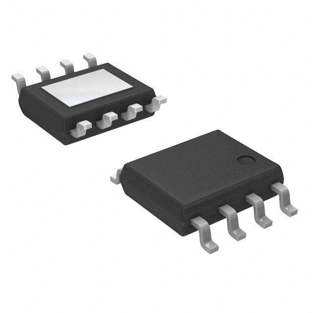
| 产品图片 |
|
| rohs | 符合RoHS无铅 / 符合限制有害物质指令(RoHS)规范要求 |
| 产品系列 | 电源管理 IC,稳压器—开关式稳压器,Texas Instruments LM2766M6/NOPB- |
| 数据手册 | |
| 产品型号 | LM2766M6/NOPB |
| PWM类型 | - |
| 产品目录页面 | |
| 产品种类 | 稳压器—开关式稳压器 |
| 供应商器件封装 | SOT-23-6 |
| 关闭 | Shutdown |
| 其它名称 | *LM2766M6/NOPB |
| 包装 | 剪切带 (CT) |
| 同步整流器 | 无 |
| 商标 | Texas Instruments |
| 安装类型 | 表面贴装 |
| 安装风格 | SMD/SMT |
| 宽度 | 1.6 mm |
| 封装 | Reel |
| 封装/外壳 | SOT-23-6 |
| 封装/箱体 | SOT-23 |
| 工作温度 | -40°C ~ 85°C |
| 工作温度范围 | - 40 C to + 85 C |
| 工厂包装数量 | 1000 |
| 开关频率 | 200 kHz |
| 拓扑结构 | Boost |
| 最大工作温度 | + 85 C |
| 最大输入电压 | 5.5 V |
| 最小工作温度 | - 40 C |
| 最小输入电压 | 1.8 V |
| 标准包装 | 1 |
| 电压-输入 | 1.8 V ~ 5.5 V |
| 电压-输出 | - |
| 电流-输出 | 20mA |
| 电源电压-最小 | 1.8 V |
| 电源电流 | 5 mA |
| 类型 | Step Up |
| 系列 | LM2766 |
| 输入电压 | 1.8 V to 5.5 V |
| 输出数 | 1 |
| 输出电压 | 3.6 V to 11 V |
| 输出电流 | 20 mA |
| 输出类型 | 可调式 |
| 频率-开关 | 200kHz |


- 商务部:美国ITC正式对集成电路等产品启动337调查
- 曝三星4nm工艺存在良率问题 高通将骁龙8 Gen1或转产台积电
- 太阳诱电将投资9.5亿元在常州建新厂生产MLCC 预计2023年完工
- 英特尔发布欧洲新工厂建设计划 深化IDM 2.0 战略
- 台积电先进制程称霸业界 有大客户加持明年业绩稳了
- 达到5530亿美元!SIA预计今年全球半导体销售额将创下新高
- 英特尔拟将自动驾驶子公司Mobileye上市 估值或超500亿美元
- 三星加码芯片和SET,合并消费电子和移动部门,撤换高东真等 CEO
- 三星电子宣布重大人事变动 还合并消费电子和移动部门
- 海关总署:前11个月进口集成电路产品价值2.52万亿元 增长14.8%


PDF Datasheet 数据手册内容提取
Product Sample & Technical Tools & Support & Folder Buy Documents Software Community LM2766 SNVS071C–MARCH2000–REVISEDSEPTEMBER2015 LM2766 Switched Capacitor Voltage Converter 1 Features 3 Description • DoublesInputSupplyVoltage The LM2766 CMOS charge-pump voltage converter 1 operates as a voltage doubler for an input voltage in • SOT-236-PinPackage the range of 1.8 V to 5.5 V. Two low-cost capacitors • 20-Ω TypicalOutputImpedance andadiodeareusedinthiscircuittoprovideupto • 90%TypicalConversionEfficiencyat20mA 20mAofoutputcurrent. • 0.1-µATypicalShutdownCurrent The LM2766 operates at 200-kHz switching frequency to reduce output resistance and voltage 2 Applications ripple. With an operating current of only 350 µA (operating efficiency greater than 90% with most • CellularPhones loads) and 0.1-µA typical shutdown current, the • Pagers LM2766 provides ideal performance for battery- • PDAs powered systems. The device is manufactured in a SOT-236-pinpackage. • OperationalAmplifierPowerSupplies • InterfacePowerSupplies DeviceInformation(1) • HandheldInstruments PARTNUMBER PACKAGE BODYSIZE(NOM) LM2766 SOT-23(6) 2.90mm×1.60mm (1) For all available packages, see the orderable addendum at theendofthedatasheet. space space space space TypicalVoltageDoublerApplication 1 An IMPORTANT NOTICE at the end of this data sheet addresses availability, warranty, changes, use in safety-critical applications, intellectualpropertymattersandotherimportantdisclaimers.PRODUCTIONDATA.
LM2766 SNVS071C–MARCH2000–REVISEDSEPTEMBER2015 www.ti.com Table of Contents 1 Features.................................................................. 1 8.3 FeatureDescription...................................................8 2 Applications........................................................... 1 8.4 DeviceFunctionalModes..........................................8 3 Description............................................................. 1 9 ApplicationandImplementation.......................... 9 4 RevisionHistory..................................................... 2 9.1 ApplicationInformation..............................................9 9.2 TypicalApplication ...................................................9 5 PinConfigurationandFunctions......................... 3 10 PowerSupplyRecommendations..................... 12 6 Specifications......................................................... 4 11 Layout................................................................... 13 6.1 AbsoluteMaximumRatings......................................4 6.2 ESDRatings..............................................................4 11.1 LayoutGuidelines.................................................13 6.3 RecommendedOperatingConditions.......................4 11.2 LayoutExample....................................................13 6.4 ThermalInformation..................................................4 12 DeviceandDocumentationSupport................. 14 6.5 ElectricalCharacteristics...........................................5 12.1 DeviceSupport......................................................14 6.6 TypicalCharacteristics .............................................6 12.2 CommunityResources..........................................14 7 ParameterMeasurementInformation..................7 12.3 Trademarks...........................................................14 7.1 TestCircuit................................................................7 12.4 ElectrostaticDischargeCaution............................14 12.5 Glossary................................................................14 8 DetailedDescription.............................................. 8 13 Mechanical,Packaging,andOrderable 8.1 Overview...................................................................8 Information........................................................... 14 8.2 FunctionalBlockDiagram.........................................8 4 Revision History NOTE:Pagenumbersforpreviousrevisionsmaydifferfrompagenumbersinthecurrentversion. ChangesfromRevisionB(May2013)toRevisionC Page • AddedDeviceInformationandPinConfigurationandFunctionssections,ESDRatingtable,FeatureDescription, DeviceFunctionalModes,ApplicationandImplementation,PowerSupplyRecommendations,Layout,Deviceand DocumentationSupport,andMechanical,Packaging,andOrderableInformationsections................................................. 1 ChangesfromRevisionA(May2013)toRevisionB Page • ChangedlayoutofNationalDataSheettoTIformat........................................................................................................... 12 2 SubmitDocumentationFeedback Copyright©2000–2015,TexasInstrumentsIncorporated ProductFolderLinks:LM2766
LM2766 www.ti.com SNVS071C–MARCH2000–REVISEDSEPTEMBER2015 5 Pin Configuration and Functions DBVPackage 6-PinSOT-23 TopView 1 6 2 5 3 4 PinFunctions PIN TYPE DESCRIPTION NO. NAME 1 V+ Power Powersupplypositivevoltageinput. 2 GND Ground Powersupplygroundinput. 3 CAP− Power Connectthispintothenegativeterminalofthecharge-pumpcapacitor. 4 SD Input Shutdowncontrolpin,tiethispintoV+innormaloperation. 5 V Power Positivevoltageoutput. OUT 6 CAP+ Power Connectthispintothepositiveterminalofthecharge-pumpcapacitor. Copyright©2000–2015,TexasInstrumentsIncorporated SubmitDocumentationFeedback 3 ProductFolderLinks:LM2766
LM2766 SNVS071C–MARCH2000–REVISEDSEPTEMBER2015 www.ti.com 6 Specifications 6.1 Absolute Maximum Ratings overoperatingfree-airtemperaturerange(unlessotherwisenoted)(1)(2) MIN MAX UNIT Supplyvoltage(V+toGND,orV+toV ) 5.8 V OUT SD (GND−0.3) (V++0.3) V V continuousoutputcurrent 40 mA OUT Outputshort-circuitdurationtoGND(3) 1 sec Continuouspowerdissipation(T =25°C)(4) 600 mW A T (4) 150 °C JMax Storagetemperature,T −65 150 °C stg (1) StressesbeyondthoselistedunderAbsoluteMaximumRatingsmaycausepermanentdamagetothedevice.Thesearestressratings only,whichdonotimplyfunctionaloperationofthedeviceattheseoranyotherconditionsbeyondthoseindicatedunderRecommended OperatingConditions.Exposuretoabsolute-maximum-ratedconditionsforextendedperiodsmayaffectdevicereliability. (2) IfMilitary/Aerospacespecifieddevicesarerequired,contacttheTISalesOffice/Distributorsforavailabilityandspecifications. (3) V maybeshortedtoGNDforonesecondwithoutdamage.Fortemperaturesabove85°C,V mustnotbeshortedtoGNDor OUT OUT devicemaybedamaged. (4) ThemaximumallowablepowerdissipationiscalculatedbyusingP =(T −T )/R ,whereT isthemaximumjunction DMax JMax A θJA JMax temperature,T istheambienttemperature,andR isthejunction-to-ambientthermalresistanceofthespecifiedpackage. A θJA 6.2 ESD Ratings VALUE UNIT Electrostatic Human-bodymodel(HBM),perANSI/ESDA/JEDECJS-001(1) ±2000 V V (ESD) discharge Machinemodel(CDM),perJEDECspecificationJESD22-C101(2) ±200 (1) JEDECdocumentJEP155statesthat500-VHBMallowssafemanufacturingwithastandardESDcontrolprocess. (2) JEDECdocumentJEP157statesthat250-VCDMallowssafemanufacturingwithastandardESDcontrolprocess. 6.3 Recommended Operating Conditions overoperatingfree-airtemperaturerange(unlessotherwisenoted) MIN NOM MAX UNIT Junctiontemperature −40 100 °C Ambienttemperature −40 85 °C Leadtemperature(soldering,10sec.) 240 °C 6.4 Thermal Information LM2766 THERMALMETRIC(1) DBV(SOT-23) UNIT 6PINS R Junction-to-ambientthermalresistance 210 °C/W θJA (1) Formoreinformationabouttraditionalandnewthermalmetrics,seetheSemiconductorandICPackageThermalMetricsapplication report,SPRA953. 4 SubmitDocumentationFeedback Copyright©2000–2015,TexasInstrumentsIncorporated ProductFolderLinks:LM2766
LM2766 www.ti.com SNVS071C–MARCH2000–REVISEDSEPTEMBER2015 6.5 Electrical Characteristics Unlessotherwisespecified,typicallimitsareforT =25°C,minimumandmaximumlimitsapplyoverthefulloperating J temperaturerange:V+=5V,C =C =10μF.(1) 1 2 PARAMETER TESTCONDITIONS MIN TYP MAX UNIT V+ Supplyvoltage 1.8 5.5 V I Supplycurrent Noload 350 950 µA Q T =25°C 0.1 0.5 µA J I Shutdownsupplycurrent SD T =85°C 0.2 A 0.6 V V Shutdownpininputvoltage SD 2 2.5V≤V ≤5.5V 20 IN I Outputcurrent mA L 1.8V≤V ≤2.5V 10 IN R Outputresistance(2) I =15mA 20 55 Ω OUT L ƒ Oscillatorfrequency See(3) 220 400 700 kHz OSC ƒ Switchingfrequency See(3) 110 200 350 kHz SW P Powerefficiency I =20mAtoGND 94% EFF L V Voltageconversionefficiency Noload 99.96% OEFF (1) Inthetestcircuit,capacitorsC andC are10-µF,0.3-ΩmaximumESRcapacitors.CapacitorswithhigherESRmayincreaseoutput 1 2 resistance,andreduceoutputvoltageandefficiency. (2) SpecifiedoutputresistanceincludesinternalswitchresistanceandcapacitorESR.SeethedetailsinApplicationandImplementationfor positivevoltagedoubler. (3) Theoutputswitchesoperateatonehalfoftheoscillatorfrequency,ƒ =2׃ . OSC SW Copyright©2000–2015,TexasInstrumentsIncorporated SubmitDocumentationFeedback 5 ProductFolderLinks:LM2766
LM2766 SNVS071C–MARCH2000–REVISEDSEPTEMBER2015 www.ti.com 6.6 Typical Characteristics (CircuitofTypicalVoltageDoublerApplication,V =5V,T =25°Cunlessotherwisespecified) IN A Figure1.SupplyCurrentvsSupplyVoltage Figure2.OutputResistancevsCapacitance Figure3.OutputResistancevsSupplyVoltage Figure4.OutputResistancevsTemperature Figure5.OutputVoltagevsLoadCurrent Figure6.SwitchingFrequencyvsSupplyVoltage 6 SubmitDocumentationFeedback Copyright©2000–2015,TexasInstrumentsIncorporated ProductFolderLinks:LM2766
LM2766 www.ti.com SNVS071C–MARCH2000–REVISEDSEPTEMBER2015 Typical Characteristics (continued) (CircuitofTypicalVoltageDoublerApplication,V =5V,T =25°Cunlessotherwisespecified) IN A Figure7. SwitchingFrequencyvsTemperature Figure8.OutputRipplevsLoadCurrent 7 Parameter Measurement Information 7.1 Test Circuit Figure9. LM2766TestCircuit Copyright©2000–2015,TexasInstrumentsIncorporated SubmitDocumentationFeedback 7 ProductFolderLinks:LM2766
LM2766 SNVS071C–MARCH2000–REVISEDSEPTEMBER2015 www.ti.com 8 Detailed Description 8.1 Overview The LM2766 CMOS charge-pump voltage converter operates as a voltage doubler for an input voltage in the rangeof1.8Vto5.5V.Twolow-costcapacitorsandadiode(neededduringstart-up)areusedinthiscircuit. 8.2 Functional Block Diagram LM2766 V+ OUT CAP+ SD Switch Array OSCILLATOR Switch Drivers CAP- GND 8.3 Feature Description 8.3.1 TestCircuit The LM2766 contains four large CMOS switches which are switched in a sequence to double the input supply voltage. Energy transfer and storage are provided by external capacitors. Figure 10 illustrates the voltage conversion scheme. When S and S are closed, C charges to the supply voltage V+. During this time interval, 2 4 1 switches S and S are open. In the next time interval, S and S are open; at the same time, S and S are 1 3 2 4 1 3 closed,thesumoftheinputvoltageV+andthevoltageacrossC givesthe2V+outputvoltagewhenthereisno 1 load. The output voltage drop when a load is added is determined by the parasitic resistance (R of the ds(on) MOSFET switches and the ESR of the capacitors) and the charge transfer loss between capacitors. See ApplicationandImplementationforfurtherdetails. Figure10. VoltageDoublingPrinciple 8.4 Device Functional Modes 8.4.1 ShutdownMode A shutdown (SD) pin is available to disable the device and reduce the quiescent current to 0.1 µA. In normal operating mode, the SD pin is connected to V+. The device can be brought into the shutdown mode by applying totheSDpinavoltagelessthan20%oftheV+pinvoltage. 8 SubmitDocumentationFeedback Copyright©2000–2015,TexasInstrumentsIncorporated ProductFolderLinks:LM2766
LM2766 www.ti.com SNVS071C–MARCH2000–REVISEDSEPTEMBER2015 9 Application and Implementation NOTE Information in the following applications sections is not part of the TI component specification, and TI does not warrant its accuracy or completeness. TI’s customers are responsible for determining suitability of components for their purposes. Customers should validateandtesttheirdesignimplementationtoconfirmsystemfunctionality. 9.1 Application Information The LM2766 provides a simple and efficient means of creating an output voltage level equal to twice that of the input voltage. Without the need of an inductor, the application solution size can be reduced versus the magnetic DC-DCconvertersolution. 9.2 Typical Application ThemainapplicationoftheLM2766istodoubletheinputvoltage. Figure11. LM2766TypicalApplication 9.2.1 DesignRequirements Fortypicalswitched-capacitorvoltageconverterapplications,usetheparameterslistedinTable1. Table1.DesignParameters DESIGNPARAMETER EXAMPLEVALUE Minimuminputvoltage 1.8to5.5V Outputcurrent(minimum),2.5V≤V ≤5.5V 20mA IN Outputcurrent(minimum),1.8V≤V ≤2.5V 10mA IN Switchingfrequency 200kHz(typical) 9.2.2 DetailedDesignProcedure 9.2.2.1 PositiveVoltageDoubler Figure12. VoltageDoublingPrinciple Copyright©2000–2015,TexasInstrumentsIncorporated SubmitDocumentationFeedback 9 ProductFolderLinks:LM2766
LM2766 SNVS071C–MARCH2000–REVISEDSEPTEMBER2015 www.ti.com The output characteristics of this circuit can be approximated by an ideal voltage source in series with a resistance. The voltage source equals 2 V+. The output resistance R is a function of the ON resistance of the out internal MOSFET switches, the oscillator frequency, and the capacitance and ESR of C and C . Because the 1 2 switching current charging and discharging C is approximately twice the output current, the effect of the ESR of 1 the pumping capacitor C is multiplied by four in the output resistance. The output capacitor C is charging and 1 2 discharging at a current approximately equal to the output current, therefore, its ESR only counts once in the outputresistance.AgoodapproximationofR is: out 2 ROUT (cid:6) 2RSW +&OSC × C1+ 4ESRC1+ ESRC2 where • R isthesumoftheONresistanceoftheinternalMOSFETswitchesshowninFigure12. (1) SW The peak-to-peak output voltage ripple is determined by the oscillator frequency as well as the capacitance and ESRoftheoutputcapacitorC : 2 I VRIPPLE = &OSC L× C2+2 × IL× ESRC2 (2) Highcapacitance,lowESRcapacitorscanreduceboththeoutputresistanceandthevoltageripple. TheSchottkydiodeD isonlyneededtoprotectthedevicefromturningonitsownparasiticdiodeandpotentially 1 latching up. During start-up, D also quickly charges up the output capacitor to V minus the diode drop thereby 1 IN decreasing the start-up time. Therefore, the Schottky diode D must have enough current carrying capability to 1 charge the output capacitor at start-up, as well as a low forward voltage to prevent the internal parasitic diode fromturningon.ASchottkydiodelike1N5817canbeusedformostapplications.Iftheinputvoltagerampisless than10V/ms,asmallerSchottkydiodelikeMBR0520LT1canbeusedtoreducethecircuitsize. 9.2.2.2 CapacitorSelection As discussed in Positive Voltage Doubler, the output resistance and ripple voltage are dependent on the capacitance and ESR values of the external capacitors. The output voltage drop is the load current times the outputresistance,andthepowerefficiencyis P I 2R D= OUT = L L PIN IL2RL+IL2ROUT +IQ(V+) where • I (V+)isthequiescentpowerlossofthedevice;and Q • I 2R istheconversionlossassociatedwiththeswitchon-resistance,thetwoexternalcapacitorsandtheir L OUT ESRs. (3) The selection of capacitors is based on the specifications of the dropout voltage (which equals I R ), the OUT OUT output voltage ripple, and the converter efficiency. Low ESR capacitors (Table 2) are recommended to maximize efficiency,reducetheoutputvoltagedropandvoltageripple. Table2.LowESRCapacitorManufacturers MANUFACTURER WEBSITE CAPACITORTYPE NichiconCorp. www.nichicon.com PL&PFseries,through-holealuminumelectrolytic AVXCorp. www.avxcorp.com TPSseries,surface-mounttantalum Sprague www.vishay.com 593D,594D,595Dseries,surface-mounttantalum Sanyo www.sanyovideo.com OS-CONseries,through-holealuminumelectrolytic Murata www.murata.com Ceramicchipcapacitors TaiyoYuden www.t-yuden.com Ceramicchipcapacitors Tokin www.tokin.com Ceramicchipcapacitors 10 SubmitDocumentationFeedback Copyright©2000–2015,TexasInstrumentsIncorporated ProductFolderLinks:LM2766
LM2766 www.ti.com SNVS071C–MARCH2000–REVISEDSEPTEMBER2015 9.2.2.3 ParallelingDevices Any number of LM2766 devices can be paralleled to reduce the output resistance. Because there is no closed loop feedback, as found in regulated circuits, stable operation is assured. Each device must have its own pumping capacitor C , while only one output capacitor C is needed as shown in Figure 13. The composite 1 OUT outputresistanceis: R of each LM2766 ROUT = OUT Number of Devices (4) Figure13. LoweringOutputResistanceByParallelingDevices 9.2.2.4 CascadingDevices Cascading the several LM2766 devices is an easy way to produce a greater voltage (a two-stage cascade circuit isshowninFigure14). Theeffectiveoutputresistanceisequaltotheweightedsumofeachindividualdevice: R =1.5R +R (5) out out_1 out_2 Note that increasing the number of cascading stages is practically limited because it significantly reduces the efficiency,increasestheoutputresistanceandoutputvoltageripple. Figure14. IncreasingOutputVoltageByCascadingDevices Copyright©2000–2015,TexasInstrumentsIncorporated SubmitDocumentationFeedback 11 ProductFolderLinks:LM2766
LM2766 SNVS071C–MARCH2000–REVISEDSEPTEMBER2015 www.ti.com 9.2.2.5 RegulatingV OUT It is possible to regulate the output of the LM2766 by use of a low dropout regulator (such as LP2980-5.0). The wholeconverterisdepictedinFigure15. AdifferentoutputvoltageispossiblebyuseofLP2980-3.3,LP2980-3.0,orLP2980-ADJ. Thefollowingconditionsmustbesatisfiedsimultaneouslyforworstcasedesign: 2V >V +V (LP2980)+I ×R (LM2766) (6) in_min out_min drop_max out_max out_max 2V <V +V (LP2980)+I ×R (LM2766) (7) in_max out_max drop_min out_min out_min Figure15. GenerateaRegulated5-VFrom3-VInputVoltage 9.2.3 ApplicationCurve Figure16.EfficiencyvsLoadCurrent 10 Power Supply Recommendations The LM2766 is designed to operate from as an inverter over an input voltage supply range from 1.8 V and 5.5 V. This input supply must be well-regulated and capable to supply the required input current. If the input supply is located far from the device, additional bulk capacitance may be required in addition to the ceramic bypass capacitors. 12 SubmitDocumentationFeedback Copyright©2000–2015,TexasInstrumentsIncorporated ProductFolderLinks:LM2766
LM2766 www.ti.com SNVS071C–MARCH2000–REVISEDSEPTEMBER2015 11 Layout 11.1 Layout Guidelines The high switching frequency and large switching currents of the LM2766 make the choice of layout important. Use the following steps as a reference to ensure the device is stable and maintains proper LED current regulationacrossitsintendedoperatingvoltageandcurrentrange. • Place C on the top layer (same layer as the LM2766) and as close to the device as possible. Connecting IN the input capacitor through short, wide traces to both the V+ and GND pins reduces the inductive voltage spikesthatoccurduringswitchingwhichcancorrupttheV+line. • Place C on the top layer (same layer as the LM2766) and as close as possible to the OUT and GND pin. OUT The returns for both C and C must come together at one point, as close to the GND pin as possible. IN OUT Connecting C through short, wide traces reduce the series inductance on the OUT and GND pins that can OUT corrupttheV andGNDlinesandcauseexcessivenoiseinthedeviceandsurroundingcircuitry. OUT • Place C1 on the top layer (same layer as the LM2766 device) and as close to the device as possible. Connecttheflyingcapacitorthroughshort,widetracestoboththeCAP+andCAP–pins. 11.2 Layout Example LM2766 V+ CAP+ GND OUT CAP- SD Figure17. LM2766LayoutExample Copyright©2000–2015,TexasInstrumentsIncorporated SubmitDocumentationFeedback 13 ProductFolderLinks:LM2766
LM2766 SNVS071C–MARCH2000–REVISEDSEPTEMBER2015 www.ti.com 12 Device and Documentation Support 12.1 Device Support 12.1.1 Third-PartyProductsDisclaimer TI'S PUBLICATION OF INFORMATION REGARDING THIRD-PARTY PRODUCTS OR SERVICES DOES NOT CONSTITUTE AN ENDORSEMENT REGARDING THE SUITABILITY OF SUCH PRODUCTS OR SERVICES OR A WARRANTY, REPRESENTATION OR ENDORSEMENT OF SUCH PRODUCTS OR SERVICES, EITHER ALONEORINCOMBINATIONWITHANYTIPRODUCTORSERVICE. 12.2 Community Resources The following links connect to TI community resources. Linked contents are provided "AS IS" by the respective contributors. They do not constitute TI specifications and do not necessarily reflect TI's views; see TI's Terms of Use. TIE2E™OnlineCommunity TI'sEngineer-to-Engineer(E2E)Community.Createdtofostercollaboration amongengineers.Ate2e.ti.com,youcanaskquestions,shareknowledge,exploreideasandhelp solveproblemswithfellowengineers. DesignSupport TI'sDesignSupport QuicklyfindhelpfulE2Eforumsalongwithdesignsupporttoolsand contactinformationfortechnicalsupport. 12.3 Trademarks E2EisatrademarkofTexasInstruments. Allothertrademarksarethepropertyoftheirrespectiveowners. 12.4 Electrostatic Discharge Caution Thesedeviceshavelimitedbuilt-inESDprotection.Theleadsshouldbeshortedtogetherorthedeviceplacedinconductivefoam duringstorageorhandlingtopreventelectrostaticdamagetotheMOSgates. 12.5 Glossary SLYZ022—TIGlossary. Thisglossarylistsandexplainsterms,acronyms,anddefinitions. 13 Mechanical, Packaging, and Orderable Information The following pages include mechanical, packaging, and orderable information. This information is the most current data available for the designated devices. This data is subject to change without notice and revision of thisdocument.Forbrowser-basedversionsofthisdatasheet,refertotheleft-handnavigation. 14 SubmitDocumentationFeedback Copyright©2000–2015,TexasInstrumentsIncorporated ProductFolderLinks:LM2766
PACKAGE OPTION ADDENDUM www.ti.com 6-Feb-2020 PACKAGING INFORMATION Orderable Device Status Package Type Package Pins Package Eco Plan Lead/Ball Finish MSL Peak Temp Op Temp (°C) Device Marking Samples (1) Drawing Qty (2) (6) (3) (4/5) LM2766M6/NOPB ACTIVE SOT-23 DBV 6 1000 Green (RoHS SN Level-1-260C-UNLIM -40 to 85 S16B & no Sb/Br) LM2766M6X/NOPB ACTIVE SOT-23 DBV 6 3000 Green (RoHS SN Level-1-260C-UNLIM -40 to 85 S16B & no Sb/Br) (1) The marketing status values are defined as follows: ACTIVE: Product device recommended for new designs. LIFEBUY: TI has announced that the device will be discontinued, and a lifetime-buy period is in effect. NRND: Not recommended for new designs. Device is in production to support existing customers, but TI does not recommend using this part in a new design. PREVIEW: Device has been announced but is not in production. Samples may or may not be available. OBSOLETE: TI has discontinued the production of the device. (2) RoHS: TI defines "RoHS" to mean semiconductor products that are compliant with the current EU RoHS requirements for all 10 RoHS substances, including the requirement that RoHS substance do not exceed 0.1% by weight in homogeneous materials. Where designed to be soldered at high temperatures, "RoHS" products are suitable for use in specified lead-free processes. TI may reference these types of products as "Pb-Free". RoHS Exempt: TI defines "RoHS Exempt" to mean products that contain lead but are compliant with EU RoHS pursuant to a specific EU RoHS exemption. Green: TI defines "Green" to mean the content of Chlorine (Cl) and Bromine (Br) based flame retardants meet JS709B low halogen requirements of <=1000ppm threshold. Antimony trioxide based flame retardants must also meet the <=1000ppm threshold requirement. (3) MSL, Peak Temp. - The Moisture Sensitivity Level rating according to the JEDEC industry standard classifications, and peak solder temperature. (4) There may be additional marking, which relates to the logo, the lot trace code information, or the environmental category on the device. (5) Multiple Device Markings will be inside parentheses. Only one Device Marking contained in parentheses and separated by a "~" will appear on a device. If a line is indented then it is a continuation of the previous line and the two combined represent the entire Device Marking for that device. (6) Lead/Ball Finish - Orderable Devices may have multiple material finish options. Finish options are separated by a vertical ruled line. Lead/Ball Finish values may wrap to two lines if the finish value exceeds the maximum column width. Important Information and Disclaimer:The information provided on this page represents TI's knowledge and belief as of the date that it is provided. TI bases its knowledge and belief on information provided by third parties, and makes no representation or warranty as to the accuracy of such information. Efforts are underway to better integrate information from third parties. TI has taken and continues to take reasonable steps to provide representative and accurate information but may not have conducted destructive testing or chemical analysis on incoming materials and chemicals. TI and TI suppliers consider certain information to be proprietary, and thus CAS numbers and other limited information may not be available for release. In no event shall TI's liability arising out of such information exceed the total purchase price of the TI part(s) at issue in this document sold by TI to Customer on an annual basis. Addendum-Page 1
PACKAGE OPTION ADDENDUM www.ti.com 6-Feb-2020 Addendum-Page 2
PACKAGE MATERIALS INFORMATION www.ti.com 20-Dec-2016 TAPE AND REEL INFORMATION *Alldimensionsarenominal Device Package Package Pins SPQ Reel Reel A0 B0 K0 P1 W Pin1 Type Drawing Diameter Width (mm) (mm) (mm) (mm) (mm) Quadrant (mm) W1(mm) LM2766M6/NOPB SOT-23 DBV 6 1000 178.0 8.4 3.2 3.2 1.4 4.0 8.0 Q3 LM2766M6X/NOPB SOT-23 DBV 6 3000 178.0 8.4 3.2 3.2 1.4 4.0 8.0 Q3 PackMaterials-Page1
PACKAGE MATERIALS INFORMATION www.ti.com 20-Dec-2016 *Alldimensionsarenominal Device PackageType PackageDrawing Pins SPQ Length(mm) Width(mm) Height(mm) LM2766M6/NOPB SOT-23 DBV 6 1000 210.0 185.0 35.0 LM2766M6X/NOPB SOT-23 DBV 6 3000 210.0 185.0 35.0 PackMaterials-Page2
PACKAGE OUTLINE DBV0006A SOT-23 - 1.45 mm max height SCALE 4.000 SMALL OUTLINE TRANSISTOR C 3.0 2.6 0.1 C 1.75 1.45 B A 1.45 MAX PIN 1 INDEX AREA 1 6 2X 0.95 3.05 2.75 1.9 5 2 4 3 0.50 6X 0.25 0.15 0.2 C A B (1.1) TYP 0.00 0.25 GAGE PLANE 0.22 TYP 0.08 8 TYP 0.6 0 0.3 TYP SEATING PLANE 4214840/B 03/2018 NOTES: 1. All linear dimensions are in millimeters. Any dimensions in parenthesis are for reference only. Dimensioning and tolerancing per ASME Y14.5M. 2. This drawing is subject to change without notice. 3. Body dimensions do not include mold flash or protrusion. Mold flash and protrusion shall not exceed 0.15 per side. 4. Leads 1,2,3 may be wider than leads 4,5,6 for package orientation. 5. Refernce JEDEC MO-178. www.ti.com
EXAMPLE BOARD LAYOUT DBV0006A SOT-23 - 1.45 mm max height SMALL OUTLINE TRANSISTOR PKG 6X (1.1) 1 6X (0.6) 6 SYMM 2 5 2X (0.95) 3 4 (R0.05) TYP (2.6) LAND PATTERN EXAMPLE EXPOSED METAL SHOWN SCALE:15X SOLDER MASK SOLDER MASK METAL UNDER METAL OPENING OPENING SOLDER MASK EXPOSED METAL EXPOSED METAL 0.07 MAX 0.07 MIN ARROUND ARROUND NON SOLDER MASK SOLDER MASK DEFINED DEFINED (PREFERRED) SOLDER MASK DETAILS 4214840/B 03/2018 NOTES: (continued) 6. Publication IPC-7351 may have alternate designs. 7. Solder mask tolerances between and around signal pads can vary based on board fabrication site. www.ti.com
EXAMPLE STENCIL DESIGN DBV0006A SOT-23 - 1.45 mm max height SMALL OUTLINE TRANSISTOR PKG 6X (1.1) 1 6X (0.6) 6 SYMM 2 5 2X(0.95) 3 4 (R0.05) TYP (2.6) SOLDER PASTE EXAMPLE BASED ON 0.125 mm THICK STENCIL SCALE:15X 4214840/B 03/2018 NOTES: (continued) 8. Laser cutting apertures with trapezoidal walls and rounded corners may offer better paste release. IPC-7525 may have alternate design recommendations. 9. Board assembly site may have different recommendations for stencil design. www.ti.com
IMPORTANTNOTICEANDDISCLAIMER TI PROVIDES TECHNICAL AND RELIABILITY DATA (INCLUDING DATASHEETS), DESIGN RESOURCES (INCLUDING REFERENCE DESIGNS), APPLICATION OR OTHER DESIGN ADVICE, WEB TOOLS, SAFETY INFORMATION, AND OTHER RESOURCES “AS IS” AND WITH ALL FAULTS, AND DISCLAIMS ALL WARRANTIES, EXPRESS AND IMPLIED, INCLUDING WITHOUT LIMITATION ANY IMPLIED WARRANTIES OF MERCHANTABILITY, FITNESS FOR A PARTICULAR PURPOSE OR NON-INFRINGEMENT OF THIRD PARTY INTELLECTUAL PROPERTY RIGHTS. These resources are intended for skilled developers designing with TI products. You are solely responsible for (1) selecting the appropriate TI products for your application, (2) designing, validating and testing your application, and (3) ensuring your application meets applicable standards, and any other safety, security, or other requirements. These resources are subject to change without notice. TI grants you permission to use these resources only for development of an application that uses the TI products described in the resource. Other reproduction and display of these resources is prohibited. No license is granted to any other TI intellectual property right or to any third party intellectual property right. TI disclaims responsibility for, and you will fully indemnify TI and its representatives against, any claims, damages, costs, losses, and liabilities arising out of your use of these resources. TI’s products are provided subject to TI’s Terms of Sale (www.ti.com/legal/termsofsale.html) or other applicable terms available either on ti.com or provided in conjunction with such TI products. TI’s provision of these resources does not expand or otherwise alter TI’s applicable warranties or warranty disclaimers for TI products. Mailing Address: Texas Instruments, Post Office Box 655303, Dallas, Texas 75265 Copyright © 2020, Texas Instruments Incorporated