ICGOO在线商城 > 集成电路(IC) > PMIC - 稳压器 - DC DC 开关稳压器 > TPS54140DGQ
 Datasheet下载
- 型号: TPS54140DGQ
- 制造商: Texas Instruments
- 库位|库存: xxxx|xxxx
- 要求:
| 数量阶梯 | 香港交货 | 国内含税 |
| +xxxx | $xxxx | ¥xxxx |
查看当月历史价格
查看今年历史价格
TPS54140DGQ产品简介:
ICGOO电子元器件商城为您提供TPS54140DGQ由Texas Instruments设计生产,在icgoo商城现货销售,并且可以通过原厂、代理商等渠道进行代购。 TPS54140DGQ价格参考。Texas InstrumentsTPS54140DGQ封装/规格:PMIC - 稳压器 - DC DC 开关稳压器, 可调式 降压 开关稳压器 IC 正 0.8V 1 输出 1.5A 10-TFSOP,10-MSOP(0.118",3.00mm 宽)裸露焊盘。您可以下载TPS54140DGQ参考资料、Datasheet数据手册功能说明书,资料中有TPS54140DGQ 详细功能的应用电路图电压和使用方法及教程。
TPS54140DGQ是由德州仪器(Texas Instruments)生产的PMIC(电源管理集成电路),属于DC-DC开关稳压器类别。它主要应用于需要高效、紧凑且可靠电源解决方案的场景中,特别是在那些对功耗和空间有严格要求的应用领域。

 应用场景

1. 通信设备:
   - TPS54140DGQ广泛用于基站、路由器、交换机等通信设备中。这些设备通常需要多个电压轨来为不同的组件供电,如处理器、FPGA、DSP等。TPS54140DGQ能够提供高效的电源转换,确保系统在高负载下依然稳定运行。

2. 工业自动化:
   - 在工业控制系统中,如PLC(可编程逻辑控制器)、传感器和执行器等,TPS54140DGQ可以为这些设备提供稳定的电源。其宽输入电压范围(4.5V至60V)使其适用于各种工业电源环境,包括电池供电和工业电网供电。

3. 汽车电子:
   - 汽车电子系统,如车载信息娱乐系统、高级驾驶辅助系统(ADAS)和车身控制模块等,都需要高性能的电源管理。TPS54140DGQ的高效率和小尺寸使其成为汽车应用的理想选择,特别是在空间有限的情况下。

4. 消费电子:
   - 在笔记本电脑、平板电脑和其他便携式设备中,TPS54140DGQ可以为处理器、内存和其他关键组件提供高效电源。其低静态电流特性有助于延长电池寿命,同时保持系统的性能。

5. 医疗设备:
   - 医疗设备如监护仪、超声波设备和便携式诊断工具等,需要高精度和可靠的电源供应。TPS54140DGQ的高效率和稳定性使其适合用于这些关键任务的应用中。

 特点和优势

- 高效率:高达95%的转换效率,减少发热并提高系统可靠性。
- 宽输入电压范围:支持4.5V至60V的输入电压,适应多种电源环境。
- 小尺寸封装:采用SOIC-8封装,节省PCB空间。
- 低静态电流:典型值仅为65µA,有助于延长电池寿命。
- 集成保护功能:内置过流保护、过温保护和短路保护,增强系统安全性。

综上所述,TPS54140DGQ凭借其高效、紧凑和可靠的特点,广泛应用于通信、工业、汽车、消费电子和医疗等多个领域。
| 参数 | 数值 |
| 产品目录 | 集成电路 (IC)半导体 |
| 描述 | IC REG BUCK ADJ 1.5A 10MSOP稳压器—开关式稳压器 3.5V-42V,1.5A Step Down SWIFT Cnvrtr |
| DevelopmentKit | TPS54140EVM-429 |
| 产品分类 | |
| 品牌 | Texas Instruments |
| 产品手册 | http://www.ti.com/litv/slvs889b |
| 产品图片 |
|
| rohs | 符合RoHS无铅 / 符合限制有害物质指令(RoHS)规范要求 |
| 产品系列 | 电源管理 IC,稳压器—开关式稳压器,Texas Instruments TPS54140DGQSWIFT™, Eco-Mode™ |
| 数据手册 | |
| 产品型号 | TPS54140DGQ |
| PWM类型 | 电流模式 |
| 产品培训模块 | http://www.digikey.cn/PTM/IndividualPTM.page?site=cn&lang=zhs&ptm=16804 |
| 产品目录页面 | |
| 产品种类 | 稳压器—开关式稳压器 |
| 供应商器件封装 | 10-MSOP-PowerPad |
| 其它名称 | 296-23970-5 |
| 制造商产品页 | http://www.ti.com/general/docs/suppproductinfo.tsp?distId=10&orderablePartNumber=TPS54140DGQ |
| 包装 | 管件 |
| 同步整流器 | 无 |
| 商标 | Texas Instruments |
| 安装类型 | 表面贴装 |
| 安装风格 | SMD/SMT |
| 封装 | Tube |
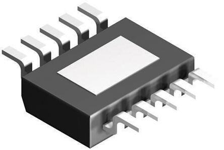
| 封装/外壳 | 10-TFSOP,10-MSOP(0.118",3.00mm 宽)裸焊盘 |
| 封装/箱体 | HVSSOP-10 |
| 工作温度 | -40°C ~ 150°C |
| 工作温度范围 | - 40 C to + 150 C |
| 工厂包装数量 | 80 |
| 开关频率 | 581 kHz |
| 拓扑结构 | Buck |
| 最大工作温度 | + 125 C |
| 最大输入电压 | 42 V |
| 最小工作温度 | - 40 C |
| 标准包装 | 80 |
| 电压-输入 | 3.5 V ~ 42 V |
| 电压-输出 | 0.8 V ~ 39 V |
| 电流-输出 | 1.5A |
| 类型 | 降压(降压) |
| 系列 | TPS54140 |
| 设计资源 | http://www.digikey.com/product-highlights/cn/zh/texas-instruments-webench-design-center/3176 |
| 输出数 | 1 |
| 输出电压 | 3.3 V |
| 输出电流 | 1.5 A |
| 输出端数量 | 1 Output |
| 输出类型 | 可调式 |
| 配用 | /product-detail/zh/TPS54140EVM-429/296-31178-ND/2232808 |
| 频率-开关 | 581kHz |


- 商务部:美国ITC正式对集成电路等产品启动337调查
- 曝三星4nm工艺存在良率问题 高通将骁龙8 Gen1或转产台积电
- 太阳诱电将投资9.5亿元在常州建新厂生产MLCC 预计2023年完工
- 英特尔发布欧洲新工厂建设计划 深化IDM 2.0 战略
- 台积电先进制程称霸业界 有大客户加持明年业绩稳了
- 达到5530亿美元!SIA预计今年全球半导体销售额将创下新高
- 英特尔拟将自动驾驶子公司Mobileye上市 估值或超500亿美元
- 三星加码芯片和SET,合并消费电子和移动部门,撤换高东真等 CEO
- 三星电子宣布重大人事变动 还合并消费电子和移动部门
- 海关总署:前11个月进口集成电路产品价值2.52万亿元 增长14.8%


PDF Datasheet 数据手册内容提取
Product Sample & Technical Tools & Support & Reference Folder Buy Documents Software Community Design TPS54140 SLVS889C–OCTOBER2008–REVISEDNOVEMBER2014 TPS54140 1.5-A, 42-V Step-Down DC-DC Converter With Eco-mode™ 1 Features 3 Description • 3.5-to42-VInputVoltageRange The TPS54140 device is a 42-V, 1.5-A, step-down 1 regulator with an integrated high-side MOSFET. • 200-mΩ High-SideMOSFET Current mode control provides simple external • HighEfficiencyatLightLoadswithaPulse compensation and flexible component selection. A SkippingEco-mode™ low-ripple pulse-skip mode reduces the no load, • 116-μAOperatingQuiescentCurrent regulated output-supply current to 116 μA. Using the enable pin, the shutdown supply current is reduced to • 1.3-μAShutdownCurrent 1.3 μA. • 100-kHzto2.5-MHzSwitchingFrequency Undervoltage lockout is internally set at 2.5 V, but • SynchronizestoExternalClock can be increased using the enable pin. The output- • AdjustableSlowStartandSequencing voltage startup ramp is controlled by the slow-start • UVandOVPower-GoodOutput pin that can also be configured for sequencing and tracking. An open-drain power-good signal indicates • AdjustableUVLOVoltageandHysteresis the output is within 94% to 107% of the nominal • 0.8-VInternalVoltageReference voltage. • MSOP10PackageWithPowerPAD™ A wide switching frequency range allows efficiency • Supportedby WEBENCH®SoftwareTool and external component size to be optimized. (www.TI.com/WEBENCH) Frequency foldback and thermal shutdown protects thedeviceduringanoverloadcondition. 2 Applications The TPS54140 device is available in a 10-pin • 12-Vand24-VIndustrialandCommercialLow thermallyenhancedMSOPPowerPADpackage. PowerSystems DeviceInformation(1) • AftermarketAutoAccessories:Video,GPS, Entertainment PARTNUMBER PACKAGE BODYSIZE(NOM) TPS54140 MSOP(10) 3.00mm×3.00mm (1) For all available packages, see the orderable addendum at theendofthedatasheet. 4 Simplified Schematic EfficiencyvsLoadCurrent VIN PWRGD 90 TPS54140 85 EN BOOT 80 % 75 PH y - nc 70 SS/TR e ci RT/CLK Effi 65 COMP VSENSE 60 VI= 12 V, V = 3.3 V, O 55 f = 1200 kHz sw GND 50 0 0.25 0.50 0.75 1 1.25 1.50 1.75 2 Load Current -A 1 An IMPORTANT NOTICE at the end of this data sheet addresses availability, warranty, changes, use in safety-critical applications, intellectualpropertymattersandotherimportantdisclaimers.PRODUCTIONDATA.
TPS54140 SLVS889C–OCTOBER2008–REVISEDNOVEMBER2014 www.ti.com Table of Contents 1 Features.................................................................. 1 8.3 FeatureDescription.................................................12 2 Applications........................................................... 1 8.4 DeviceFunctionalModes........................................27 3 Description............................................................. 1 9 ApplicationandImplementation........................ 29 4 SimplifiedSchematic............................................. 1 9.1 ApplicationInformation............................................29 9.2 TypicalApplication..................................................29 5 RevisionHistory..................................................... 2 10 PowerSupplyRecommendations..................... 40 6 PinConfigurationandFunctions......................... 3 11 Layout................................................................... 40 7 Specifications......................................................... 4 11.1 LayoutGuidelines.................................................40 7.1 AbsoluteMaximumRatings .....................................4 11.2 LayoutExample....................................................41 7.2 HandlingRatings.......................................................4 12 DeviceandDocumentationSupport................. 41 7.3 RecommendedOperatingConditions.......................4 7.4 ThermalInformation..................................................5 12.1 DeviceSupport......................................................41 7.5 ElectricalCharacteristics...........................................5 12.2 DocumentationSupport........................................41 7.6 TypicalCharacteristics..............................................6 12.3 Trademarks...........................................................42 12.4 ElectrostaticDischargeCaution............................42 8 DetailedDescription............................................ 11 12.5 Glossary................................................................42 8.1 Overview.................................................................11 13 Mechanical,Packaging,andOrderable 8.2 FunctionalBlockDiagram.......................................12 Information........................................................... 42 5 Revision History ChangesfromRevisionB(September2013)toRevisionC Page • AddedtheHandlingRatingstableandthefollowingsections:FeatureDescription,DeviceFunctionalModes, ApplicationandImplementation,PowerSupplyRecommendations,DeviceandDocumentationSupport,and Mechanical,Packaging,andOrderableInformation............................................................................................................... 1 ChangesfromRevisionA(August2012)toRevisionB Page • DeletedSWIFTfromthedatasheetTitleandFeatures......................................................................................................... 1 ChangesfromOriginal(October2008)toRevisionA Page • ChangedFeaturesItemFrom:300kHzto2.5MHzSwitchingFrequencyTo:100kHzto2.5MHzSwitchingFrequency......1 • ChangedDescriptiontextFrom:"within93%to107%ofitsnomvoltage."To:"within94%to107%ofitsnomvoltage."...1 • ChangedEnablethreshold+50mVTYPvalueFrom:±3.8To:–3.8..................................................................................... 5 • ChangedEnablethreshold±50mVTYPvalueFrom:±0.9To:–0.98................................................................................... 5 • ChangedHysteresiscurrentTYPvalueFrom:±2.9To:–2.9................................................................................................ 5 • ChangedErroramplifiertransconductance(g )TestConditionFrom:±2μA<I <2μA,V =1VTo:–2μA M COMP COMP <I <2μA,V =1V................................................................................................................................................... 5 COMP COMP • ChangedErroramplifiertransconductance(g )duringslowstartFrom:±2μA<I <2μA,V =1VTo:–2 M COMP COMP μA<I <2μA,V =1V.............................................................................................................................................. 5 COMP COMP • ChangedtextintheErrorAmplifiersectionFrom:"thegmis25μA/V"To:"thegmis26μA/V" ....................................... 14 • ChangedtextintheSlowStartandTrackingPin(SS/TR)sectionFrom:"VINUVLOisexceeded,ENpinpulled below1.25V"To:"VINpinisbelowtheVINUVLO,ENpinpulledbelow1.25V"................................................................ 15 • ChangedStartInputVoltage(risingVIN)voltageFrom:7.25VTo:7.7V........................................................................... 29 • ChangedStartInputVoltage(fallingVIN)voltageFrom:6.25VTo:6.7V.......................................................................... 29 • ChangedEquation29........................................................................................................................................................... 30 • Changed7.25Vto7.7Vand6.25Vto6.7VintheUnderVoltageLockOutSetPointsection............................................ 34 • ChangedEquation47........................................................................................................................................................... 36 • ChangedEquation49........................................................................................................................................................... 36 2 SubmitDocumentationFeedback Copyright©2008–2014,TexasInstrumentsIncorporated ProductFolderLinks:TPS54140
TPS54140 www.ti.com SLVS889C–OCTOBER2008–REVISEDNOVEMBER2014 6 Pin Configuration and Functions DGQPackage 10-PinMSOPWithPowerPAD™ TopView BOOT 1 10 PH VIN 2 9 GND Thermal Pad (11) EN 3 8 COMP SS/TR 4 7 VSENSE RT/CLK 5 6 PWRGD PinFunctions PIN I/O DESCRIPTION NO. NAME AbootstrapcapacitorisrequiredbetweentheBOOTandPHpins.Ifthevoltageonthiscapacitorisbelow 1 BOOT O theminimumrequiredbythedevice,theoutputisforcedtoswitchoffuntilthecapacitorisrefreshed. 2 VIN I Thispinisthe3.5-to42-Vinputsupplyvoltage. Thispinistheenablepinandinternalpullupcurrentsource.Todisable,pullbelow1.2V.Floatthispinto 3 EN I enable.Adjusttheinputundervoltagelockoutwithtworesistors. Thispinistheslow-startandtrackingpin.Anexternalcapacitorconnectedtothispinsetstheoutputrise 4 SS/TR I time.Becausethevoltageonthispinoverridestheinternalreference,itcanbeusedfortrackingand sequencing. Thispinistheresistortimingandexternalclockpin.Aninternalamplifierholdsthispinatafixedvoltage whenusinganexternalresistortogroundtosettheswitchingfrequency.IfthepinispulledabovethePLL 5 RT/CLK I upperthreshold,amodechangeoccursandthepinbecomesasynchronizationinput.Theinternalamplifier isdisabledandthepinisahighimpedanceclockinputtotheinternalPLL.Ifclockingedgesstop,the internalamplifierisre-enabledandthemodereturnstoaresistorsetfunction. Thispinisanopendrainoutput.Thispinisassertedlowiftheoutputvoltageislowbecauseofthermal 6 PWRGD O shutdown,dropout,overvoltage,orENshutdown. 7 VSENSE I Thispinistheinvertingnodeofthetransconductance(gm)erroramplifier. Thispinistheerroramplifieroutputandinputtotheoutput-switchcurrentcomparator.Connectfrequency 8 COMP O compensationcomponentstothispin. 9 GND — Groundpin 10 PH O Thispinisthesourceoftheinternalhigh-sidepowerMOSFET. TheGNDpinmustbeelectricallyconnectedtotheexposedpadontheprintedcircuitboardforproper 11 ThermalPad — operation. Copyright©2008–2014,TexasInstrumentsIncorporated SubmitDocumentationFeedback 3 ProductFolderLinks:TPS54140
TPS54140 SLVS889C–OCTOBER2008–REVISEDNOVEMBER2014 www.ti.com 7 Specifications 7.1 Absolute Maximum Ratings(1) Overoperatingtemperaturerange(unlessotherwisenoted). MIN MAX UNIT VIN –0.3 47 EN –0.3 5 BOOT 55 VSENSE –0.3 3 Inputvoltage V COMP –0.3 3 PWRGD –0.3 6 SS/TR –0.3 3 RT/CLK –0.3 3.6 PH–BOOT 8 Outputvoltage PH –0.6 47 V PH,10-nsTransient –2 47 VoltageDifference PADtoGND ±200 mV EN 100 μA BOOT 100 mA Sourcecurrent VSENSE 10 μA PH CurrentLimit A RT/CLK 100 μA VIN CurrentLimit A COMP 100 μA Sinkcurrent PWRGD 10 mA SS/TR 200 μA Operatingjunctiontemperature –40 150 °C (1) Stressesbeyondthoselistedunderabsolutemaximumratingsmaycausepermanentdamagetothedevice.Thesearestressratings onlyandfunctionaloperationofthedeviceattheseoranyotherconditionsbeyondthoseindicatedunderrecommendedoperating conditionsisnotimplied.Exposuretoabsolute-maximum-ratedconditionsforextendedperiodsmayaffectdevicereliability. 7.2 Handling Ratings MIN MAX UNIT T Storagetemperaturerange –65 150 °C stg Humanbodymodel(HBM),perANSI/ESDA/JEDECJS-001,all pins(1) –1 1 kV V Electrostaticdischarge (ESD) Chargeddevicemodel(CDM),perJEDECspecification JESD22-C101,allpins(2) –500 500 V (1) JEDECdocumentJEP155statesthat500-VHBMallowssafemanufacturingwithastandardESDcontrolprocess. (2) JEDECdocumentJEP157statesthat250-VCDMallowssafemanufacturingwithastandardESDcontrolprocess. 7.3 Recommended Operating Conditions Overoperatingfree-airtemperaturerange(unlessotherwisenoted) MIN NOM MAX UNIT OperatinginputvoltageontheVINpin 3.5 42 V Outputvoltage 0.8 39 V Outputcurrent 0 1.5 A T Operatingjunctiontemperature –40 150 °C J 4 SubmitDocumentationFeedback Copyright©2008–2014,TexasInstrumentsIncorporated ProductFolderLinks:TPS54140
TPS54140 www.ti.com SLVS889C–OCTOBER2008–REVISEDNOVEMBER2014 7.4 Thermal Information DGQ THERMALMETRIC(1) UNIT 10PINS R Junction-to-ambientthermalresistance 67.4 θJA R Junction-to-case(top)thermalresistance 46.7 θJC(top) R Junction-to-boardthermalresistance 38.4 θJB °C/W ψ Junction-to-topcharacterizationparameter 1.9 JT ψ Junction-to-boardcharacterizationparameter 38.4 JB R Junction-to-case(bottom)thermalresistance 46.7 θJC(bot) (1) Formoreinformationabouttraditionalandnewthermalmetrics,seetheICPackageThermalMetricsapplicationreport,SPRA953. 7.5 Electrical Characteristics T =–40°Cto150°C,VIN=3.5to42V(unlessotherwisenoted) J PARAMETER TESTCONDITIONS MIN TYP MAX UNIT SUPPLYVOLTAGE(VINPIN) Operatinginputvoltage 3.5 42 V Internalundervoltagelockoutthreshold Novoltagehysteresis,risingandfalling 2.5 V Shutdownsupplycurrent EN=0V,25°C,3.5V≤VIN≤42V 1.3 4 μA Operating:nonswitchingsupplycurrent VSENSE=0.83V,VIN=12V,25°C 116 136 ENABLEANDUVLO(ENPIN) Enablethresholdvoltage Novoltagehysteresis,risingandfalling,25°C 0.9 1.25 1.55 V Enablethreshold50mV –3.8 Inputcurrent μA Enablethreshold±50mV –0.9 Hysteresiscurrent –2.9 μA VOLTAGEREFERENCE T =25°C 0.792 0.8 0.808 J Voltagereference V 0.784 0.8 0.816 HIGH-SIDEMOSFET VIN=3.5V,BOOT-PH=3V 300 On-resistance mΩ VIN=12V,BOOT-PH=6V 200 410 ERRORAMPLIFIER Inputcurrent 50 nA Erroramplifiertransconductance(g ) –2μA<I <2μA,V =1V 97 μMhos M COMP COMP Erroramplifiertransconductance(gM) –2μA<ICOMP<2μA,VCOMP=1V, 26 μMhos duringslowstart V =0.4V VSENSE Erroramplifierdcgain V =0.8V 10000 V/V VSENSE Erroramplifierbandwidth 2700 kHz Erroramplifiersource/sink V =1V,100mVoverdrive ±7 μA (COMP) COMPtoswitchcurrent 6 A/V transconductance CURRENTLIMIT Currentlimitthreshold VIN=12V,T =25°C 1.8 2.7 A J THERMALSHUTDOWN Thermalshutdown 182 °C TIMINGRESISTORANDEXTERNALCLOCK(RT/CLKPIN) SwitchingFrequencyRangeusingRT 100 2500 kHz mode f Switchingfrequency R =200kΩ 450 581 720 kHz SW T SwitchingFrequencyRangeusingCLK 300 2200 kHz mode Copyright©2008–2014,TexasInstrumentsIncorporated SubmitDocumentationFeedback 5 ProductFolderLinks:TPS54140
TPS54140 SLVS889C–OCTOBER2008–REVISEDNOVEMBER2014 www.ti.com Electrical Characteristics (continued) T =–40°Cto150°C,VIN=3.5to42V(unlessotherwisenoted) J PARAMETER TESTCONDITIONS MIN TYP MAX UNIT MinimumCLKpulsewidth 40 ns RT/CLKhighthreshold 1.9 2.2 V RT/CLKlowthreshold 0.5 0.7 V RT/CLKfallingedgetoPHrisingedge Measuredat500kHzwithRTresistorinseries 60 ns delay PLLlockintime Measuredat500kHz 100 μs SLOWSTARTANDTRACKING(SS/TR) Chargecurrent V =0.4V 2 μA SS/TR SS/TR-to-VSENSEmatching V =0.4V 45 mV SS/TR SS/TR-to-referencecrossover 98%nominal 1.0 V SS/TRdischargecurrent(overload) VSENSE=0V,V(SS/TR)=0.4V 112 μA SS/TRdischargevoltage VSENSE=0V 54 mV POWERGOOD(PWRGDPIN) VSENSEfalling 92% VSENSErising 94% V VSENSEthreshold VSENSE VSENSErising 109% VSENSEfalling 107% Hysteresis VSENSEfalling 2% Outputhighleakage VSENSE=VREF,V(PWRGD)=5.5V,25°C 10 nA Onresistance I(PWRGD)=3mA,VSENSE<0.79V 50 Ω MinimumVINfordefinedoutput V(PWRGD)<0.5V,II(PWRGD)=100μA 0.95 1.5 V 7.6 Typical Characteristics W 0.816 m 500 nce - VI= 12 V VI= 12 V a st n-Source On-State Resi 235705 BOOT-PH = 3 V BOOT-PH = 6 V Voltage Reference - V 00..880008 c Drai 125 V- ref 0.792 ati St N - O DS 0 0.784 R -50 -25 0 25 50 75 100 125 150 -50 -25 0 25 50 75 100 125 150 TJ- Junction Temperature - °C TJ- Junction Temperature - °C Figure1.OnResistancevsJunctionTemperature Figure2.VoltageReferencevsJunctionTemperature 6 SubmitDocumentationFeedback Copyright©2008–2014,TexasInstrumentsIncorporated ProductFolderLinks:TPS54140
TPS54140 www.ti.com SLVS889C–OCTOBER2008–REVISEDNOVEMBER2014 Typical Characteristics (continued) 3.5 610 V= 12 V, V= 12 V I I RT= 200 kW 600 Hz k A 3 cy - 590 nt - uen e q Switch Curr2.5 witching Fre 557800 S - fs 560 2 550 -50 -25 0 25 50 75 100 125 150 -50 -25 0 25 50 75 100 125 150 TJ- Junction Temperature - °C TJ- Junction Temperature - °C Figure3.SwitchCurrentLimitvsJunctionTemperature Figure4.SwitchingFrequencyvsJunctionTemperature 2500 500 V= 12 V, I T = 25°C J kHz 2000 Hz) 400 ching Frequency - 11050000 hing Frequency (k 230000 Swit witc - S 100 fs 500 0 0 200 300 400 500 600 700 800 900 1000 1100 1200 0 25 50 75 100 125 150 175 200 RT/CLK - Resistance - kW RT/CLK Resistance (kW) C006 Figure5.SwitchingFrequencyvsRT/CLKResistance,High Figure6.SwitchingFrequencyvsRT/CLKResistance,Low FrequencyRange FrequencyRange 40 150 V= 12 V I V= 12 V I 130 30 110 V V A/ A/ m m m - m - g g 90 20 70 50 10 -50 -25 0 25 50 75 100 125 150 -50 -25 0 25 50 75 100 125 150 TJ- Junction Temperature - °C TJ- Junction Temperature - °C Figure7.EATransconductanceDuringSlowStartvs Figure8.EATransconductancevsJunctionTemperature JunctionTemperature Copyright©2008–2014,TexasInstrumentsIncorporated SubmitDocumentationFeedback 7 ProductFolderLinks:TPS54140
TPS54140 SLVS889C–OCTOBER2008–REVISEDNOVEMBER2014 www.ti.com Typical Characteristics (continued) 1.40 -3.25 V= 12 V VI= 12 V, I VI(EN)=Threshold +50 mV -3.5 V1.30 d - ol A h m EN - Thres1.20 I-(EN)-3.75 -4 1.10 -4.25 -50 -25 0 25 50 75 100 125 150 -50 -25 0 25 50 75 100 125 150 TJ- Junction Temperature - °C TJ- Junction Temperature - °C Figure9.ENPinVoltagevsJunctionTemperature Figure10.ENPinCurrentvsJunctionTemperature -0.8 -1 VI= 12 V, VI= 12 V VI(EN)=Threshold -50 mV -0.85 -1.5 Am Am I-(EN)-0.9 I-(SS/TR) -2 -0.95 -2.5 -1 -3 -50 -25 0 25 50 75 100 125 150 -50 -25 0 25 50 75 100 125 150 TJ- Junction Temperature - °C TJ- Junction Temperature - °C Figure11.ENPinCurrentvsJunctionTemperature Figure12.SS/TRChargeCurrentvsJunctionTemperature 120 100 VI= 12 V VI= 12 V, T = 25°C J 80 115 w I-AmI(SS/TR)110 % of Nominal fs 4600 105 20 100 0 -50 -25 0 25 50 75 100 125 150 0 0.2 0.4 0.6 0.8 TJ- Junction Temperature - °C VSENSE- V Figure13.SS/TRDischargeCurrentvsJunction Figure14.SwitchingFrequencyvsVSENSE Temperature 8 SubmitDocumentationFeedback Copyright©2008–2014,TexasInstrumentsIncorporated ProductFolderLinks:TPS54140
TPS54140 www.ti.com SLVS889C–OCTOBER2008–REVISEDNOVEMBER2014 Typical Characteristics (continued) 2 2 V= 12 V I T = 25°C J 1.5 1.5 A A m m I-(VIN) 1 I-(VIN) 1 0.5 0.5 0 0 -50 -25 0 25 50 75 100 125 150 0 10 20 30 40 TJ- Junction Temperature - °C VI- Input Voltage - V Figure15.ShutdownSupplyCurrentvsJunction Figure16.ShutdownSupplyCurrentvsInputVoltage(V ) IN Temperature 140 140 VI= 12 V, TJ= 25oC, VI(VSENSE)= 0.83 V VI(VSENSE)= 0.83 V 130 130 120 120 A A m m I-(VIN) 110 I-(VIN) 110 100 100 90 90 -50 -25 0 25 50 75 100 125 150 0 20 40 TJ- Junction Temperature - °C VI- Input Voltage - V Figure17.VINSupplyCurrentvsJunctionTemperature Figure18.VINSupplyCurrentvsInputVoltage 100 115 V= 12 V V= 12 V I I 80 ef110 VSENSE Rising Vr of % 105 VSENSE Falling WDSON - 60 eshold - 100 R 40 Thr GD 95 VSENSE Rising R W 20 P 90 VSENSE Falling 0 -50 -25 0 25 50 75 100 125 150 85 -50 -25 0 25 50 75 100 125 150 TJ- Junction Temperature - °C TJ- Junction Temperature - °C Figure19.PWRGDOnResistancevsJunctionTemperature Figure20.PWRGDThresholdvsJunctionTemperature Copyright©2008–2014,TexasInstrumentsIncorporated SubmitDocumentationFeedback 9 ProductFolderLinks:TPS54140
TPS54140 SLVS889C–OCTOBER2008–REVISEDNOVEMBER2014 www.ti.com Typical Characteristics (continued) 2.5 3 2.3 2.75 V V- I(BOOT-PH) 2 V- VI(VIN) 2.50 1.8 2.25 1.5 2 -50 -25 0 25 50 75 100 125 150 -50 -25 0 25 50 75 100 125 150 TJ- Junction Temperature - °C TJ- Junction Temperature - °C Figure21.BOOT-PHUVLOvsJunctiontemperature Figure22.InputVoltage(UVLO)vsJunctionTemperature 500 60 VTJI== 1225 oVC, 55 VV(IS=S/ T1R)2= V0.2 V 400 50 V 300 V m m Offset - 200 Offset - 45 40 100 35 0 30 0 100 200 300 400 500 600 700 800 -50 -25 0 25 50 75 100 125 150 VSENSE - mV TJ- Junction Temperature - °C Figure23.SS/TRtoVSENSEOffsetvsVSENSE Figure24.SS/TRtoVSENSEOffsetvsTemperature 10 SubmitDocumentationFeedback Copyright©2008–2014,TexasInstrumentsIncorporated ProductFolderLinks:TPS54140
TPS54140 www.ti.com SLVS889C–OCTOBER2008–REVISEDNOVEMBER2014 8 Detailed Description 8.1 Overview The TPS54140 device is a 42-V, 1.5-A, step-down (buck) regulator with an integrated high-side n-channel MOSFET. To improve performance during line and load transients, the device implements a constant-frequency, current mode control which reduces output capacitance and simplifies external frequency compensation design. The wide switching frequency of 100 kHz to 2500 kHz allows for efficiency and size optimization when selecting the output filter components. The switching frequency is adjusted using a resistor to ground on the RT/CLK pin. The device has an internal phase-lock loop (PLL) on the RT/CLK pin that is used to synchronize the power- switchturnontoafallingedgeofanexternalsystemclock. The TPS54140 device has a default startup voltage of approximately 2.5 V. The EN pin has an internal pullup current-source that can be used to adjust the input-voltage undervoltage-lockout (UVLO) threshold with two external resistors. In addition, the pullup current provides a default condition. The device operates when the EN pin is floating. The operating current is 116 μA when not switching and under no load. When the device is disabled,thesupplycurrentis1.3μA. The integrated 200-mΩ high-side MOSFET allows for high-efficiency power-supply designs capable of delivering 1.5 A of continuous current to a load. The TPS54140 device reduces the external component count by integrating the boot-recharge diode. The bias voltage for the integrated high-side MOSFET is supplied by a capacitorontheBOOTtoPHpin.Theboot-capacitorvoltageismonitoredbyanUVLOcircuitandturnsthehigh- side MOSFET off when the boot voltage falls below a preset threshold. The TPS54140 device can operate at high duty cycles because of the boot UVLO. The output voltage can be stepped down to as low as the 0.8-V reference. The TPS54140 device has a power good comparator (PWRGD) which asserts when the regulated output voltage is less than 92% or greater than 109% of the nominal output voltage. The PWRGD pin is an open drain output which deasserts when the VSENSE pin voltage is between 94% and 107% of the nominal output voltage allowingthepintotransitionhighwhenapullupresistorisused. The TPS54140 device minimizes excessive-output overvoltage (OV) transients by taking advantage of the OV power-good comparator. When the OV comparator is activated, the high-side MOSFET is turned off and masked fromturningonuntiltheoutputvoltageislowerthan107%. The SS/TR (slow start/tracking) pin is used to minimize inrush currents or provide power-supply sequencing during power up. A small value capacitor should be coupled to the pin to adjust the slow-start time. A resistor dividercanbecoupledtothepinforcriticalpower-supplysequencingrequirements.TheSS/TRpinisdischarged before the output powers up. This discharging ensures a repeatable restart after an over-temperature fault, UVLOfault,oradisabledcondition. The TPS54140 device also discharges the slow-start capacitor during overload conditions with an overload recovery circuit. The overload recovery circuit slow starts the output from the fault voltage to the nominal regulation voltage when a fault condition is removed. A frequency -foldback circuit reduces the switching frequencyduringstartupandovercurrentfaultconditionstohelpcontroltheinductorcurrent. Copyright©2008–2014,TexasInstrumentsIncorporated SubmitDocumentationFeedback 11 ProductFolderLinks:TPS54140
TPS54140 SLVS889C–OCTOBER2008–REVISEDNOVEMBER2014 www.ti.com 8.2 Functional Block Diagram PWRGD EN VIN 6 3 2 Shutdown Thermal Shutdown UVLO Enable UO Logic Comparator Shutdown Shutdown Logic OV Enable Threshold Boot Charge Voltage Minimum Boot Reference Clamp UVLO Current Pulse Sense ERROR Skip AMPLIFIER PWM VSENSE 7 Comparator 1 BOOT SS/TR 4 Logic And PWM Latch Shutdown Slope Compensation COMP 8 10 PH 11 POWERPAD Frequency Shift Overload Maximum Recovery Clamp Oscillator TPS54140Block Diagram 9 GND with PLL 5 RT/CLK 8.3 Feature Description 8.3.1 FixedFrequencyPWMControl The TPS54140 device uses an adjustable fixed-frequency, peak-current mode control. The output voltage is compared through external resistors on the VSENSE pin to an internal voltage reference by an error amplifier which drives the COMP pin. An internal oscillator initiates the turn on of the high-side MOSFET power switch. The error amplifier output is compared to the high-side MOSFET power-switch current. When the power-switch current reaches the COMP voltage level the power switch is turned off. The COMP pin voltage increases and decreases as the output current increases and decreases. The device implements a current limit by clamping the COMPpinvoltagetoamaximumlevel.TheEco-modeisimplementedwithaminimumclampontheCOMPpin. 8.3.2 SlopeCompensationOutputCurrent The TPS54140 device adds a compensating ramp to the switch-current signal. This slope compensation prevents sub-harmonic oscillations. The available peak inductor current remains constant over the full duty-cycle range. 12 SubmitDocumentationFeedback Copyright©2008–2014,TexasInstrumentsIncorporated ProductFolderLinks:TPS54140
TPS54140 www.ti.com SLVS889C–OCTOBER2008–REVISEDNOVEMBER2014 Feature Description (continued) 8.3.3 BootstrapVoltage(BOOT) The TPS54140 device has an integrated boot regulator and requires a small ceramic capacitor between the BOOT and PH pins to provide the gate-drive voltage for the high-side MOSFET. The value of the ceramic capacitor should be 0.1 μF. A ceramic capacitor with an X7R- or X5R-grade dielectric is recommended because of the stable characteristics over temperature and voltage. To improve drop out, the TPS54140 device is designed to operate at 100% duty cycle as long as the BOO-to-PH pin voltage is greater than 2.1 V. When the voltage from the BOOT to PH pins drops below 2.1 V, the high-side MOSFET is turned off using an UVLO circuit allowing for the low-side diode to conduct which allows refreshing of the BOOT capacitor. Because the supply currentsourcedfromtheBOOTcapacitorislow,thehigh-sideMOSFETcanremainonformoreswitchingcycles thanitrefreshes,thus,theeffectiveduty-cyclelimitationthatisattributedtothebootregulatorsystemishigh. 8.3.4 LowDropoutOperation The duty cycle during dropout of the regulator is mainly determined by the voltage drops across the power MOSFET, inductor, low-side diode, and printed circuit-board resistance. During operating conditions in which the input voltage drops, the high-side MOSFET can remain on for 100% of the duty cycle to maintain output regulationoruntiltheBOOT-to-PHvoltagefallsbelow2.1V. When the high-side MOSFET is off, the low-side diode conducts and the BOOT capacitor recharges. During this boot-capacitor recharge time, the inductor current ramps down until the high-side MOSFET turns on. The recharge time is longer than the typical high-side MOSFET off time of previous switching cycles, and thus, the inductor current ripple is larger. The larger ripple current results in more ripple voltage on the output. The recharge time is a function of the input voltage, boot capacitor value, and the impedance of the internal boot- rechargediode. Attention must be given to maximum duty-cycle applications that experience extended time periods without a load current. The high-side MOSFET turns off when the voltage across the BOOT capacitors falls below the 2.1- V threshold in applications that have a difference in the input voltage and output voltage that is less than 3 V. However, the inductor does not have enough current to pull the PH pin down to recharge the boot capacitor. The regulator does not switch because the boot capacitor is less than 2.1 V and the output capacitor decays until the difference in the input voltage and output voltage is 2.1 V. At this time the boot undervoltage lockout is exceeded andthedeviceswitchesuntilthedesiredoutputvoltageisreached. Figure 25 and Figure 26 show the start and stop voltages for 3.3-V and 5-V applications. The voltages are plotted versus the load current. The start voltage is defined as the input voltage required to regulate the output voltage with 1%. The stop voltage is defined as the input voltage at which the output drops by 5% or stops switching. 4 5.6 VO= 3.3 V VO= 5 V 3.8 5.4 V- Input Voltage - VI 33..46 SSttaorpt V- Input Voltage - VI 5.52 Start Stop 3.2 4.8 3 4.6 0 0.05 0.10 0.15 0.20 0 0.05 0.10 0.15 0.20 IO- Output Current -A IO- Output Current -A Figure25.3.3-VStartandStopVoltage Figure26.5-VStartandStopVoltage Copyright©2008–2014,TexasInstrumentsIncorporated SubmitDocumentationFeedback 13 ProductFolderLinks:TPS54140
TPS54140 SLVS889C–OCTOBER2008–REVISEDNOVEMBER2014 www.ti.com Feature Description (continued) 8.3.5 ErrorAmplifier The TPS54140 device has a transconductance amplifier for the error amplifier. The error amplifier compares the VSENSE voltage to the lower voltage of either the SS/TR pin voltage or the internal 0.8-V voltage reference. The transconductance (gm) of the error amplifier is 97 μA/V during normal operation. During the slow-start operation, thetransconductanceisafractionofthenormaloperatinggm.WhenthevoltageoftheVSENSEpinisbelow0.8 VandthedeviceisregulatingusingtheSS/TRvoltage,thegmis26 μA/V. The frequency compensation components (capacitor, series resistor, and capacitor) are added to the COMP pin toground. 8.3.6 VoltageReference The voltage reference system produces a precise ±2% voltage reference over temperature by scaling the output ofatemperature-stablebandgapcircuit. 8.3.7 AdjustingtheOutputVoltage The output voltage is set with a resistor divider from the output node to the VSENSE pin. Using divider resistors with a tolerance of 1% or better is recommended. Begin with a value of 10 kΩ for the R2 resistor and use Equation 1 to calculate the value of R1. To improve efficiency at very light loads, consider using larger value resistors. If the values are too high the regulator will be more susceptible to noise and voltage errors from the VSENSEinputcurrentwillbenoticeable æ(VOUT -0.8V)ö R1=R2´ç ÷ ç 0.8V ÷ è ø (1) 8.3.8 EnableandAdjustingUndervoltageLockout The TPS54140 device is disabled when the VIN pin voltage falls below 2.5 V. If an application requires a higher undervoltage lockout (UVLO), use the EN pin as shown in Figure 27 to adjust the input voltage UVLO by using the two external resistors. Using the UVLO to adjust registers is not required but is highly recommended for operation to provide consistent power-up behavior. The EN pin has an internal pullup-current source, I1, of 0.9 μA that provides the default condition of the TPS54140 device while operating when the EN pin is floating. When the EN pin voltage exceeds 1.25 V, an additional 2.9 μA of hysteresis, Ihys, is added. This additional current facilitatesinputvoltagehysteresis.UseEquation2tocalculateR1whichsetstheexternalhysteresisfortheinput voltage.UseEquation3 tocalculateR2whichsetstheinputstartvoltage. TPS54140 VIN Ihys I1 R1 0.9mA 2.9mA + R2 EN 1.25 V - Figure27. AdjustableUndervoltageLockout(UVLO) V -V R1= START STOP I HYS (2) V R2= ENA V -V START ENA +I R1 1 (3) 14 SubmitDocumentationFeedback Copyright©2008–2014,TexasInstrumentsIncorporated ProductFolderLinks:TPS54140
TPS54140 www.ti.com SLVS889C–OCTOBER2008–REVISEDNOVEMBER2014 Feature Description (continued) Figure 28 shows another technique for adding input voltage hysteresis. This method can be used if the resistance values are high from the previous method and a wider voltage hysteresis is needed. The resistor, R3, sourcesadditionalhysteresiscurrentintotheENpin. TPS54140 VIN Ihys R1 I1 2.9mA 0.9mA + R2 EN 1.25 V - VOUT R3 Figure28. AddingAdditionalHysteresis V -V R1= START STOP V I + OUT HYS R3 (4) V R2= ENA V -V V START ENA +I - ENA R1 1 R3 (5) 8.3.9 SlowStartandTrackingPin(SS/TR) The TPS54140 device effectively uses the lower voltage of the internal voltage reference or the SS/TR pin voltage as the reference voltage of the power supply and regulates the output accordingly. A capacitor on the SS/TR pin to ground implements a slow-start time. The TPS54140 device has an internal pullup-current source of 2 μA that charges the external slow-start capacitor. Use Equation 6 to calculate the value of the slow-start capacitor, C , which sets the slow-start time, t (10% to 90%). The slow-start capacitor should remain lower SS SS than0.47μFandgreaterthan0.47nF. CSS(nF)= tSSVR(mEFs()V´I)S´S0(.m8A) where • Thevoltagereference(V )is0.8V REF • Theslowstartcurrent(I )is2μA (6) SS At power up, the TPS54140 device does not begin switching until the slow-start pin is discharged to less than 40 mVtoensureaproperpowerup(seeFigure29). Also, during normal operation, the TPS54140 device stops switching and the SS/TR must be discharged to 40 mV when the voltage at the VIN pin is below the VIN UVLO, EN pin pulled below 1.25 V, or a thermal shutdown eventoccurs. The VSENSE voltage follows the SS/TR pin voltage with a 45-mV offset up to 85% of the internal voltage reference. When the SS/TR voltage is greater than 85% on the internal reference voltage the offset increases as the effective system reference transitions from the SS/TR voltage to the internal voltage reference (see Figure23).TheSS/TRvoltagerampslinearlyuntilclampedat1.7V. Copyright©2008–2014,TexasInstrumentsIncorporated SubmitDocumentationFeedback 15 ProductFolderLinks:TPS54140
TPS54140 SLVS889C–OCTOBER2008–REVISEDNOVEMBER2014 www.ti.com Feature Description (continued) EN SS/TR V SENSE VOUT Figure29. OperationofSS/TRPinWhenStarting 8.3.10 Overload-RecoveryCircuit The TPS54140 device has an overload-recovery (OLR) circuit. The OLR circuit slow starts the output from the overload voltage to the nominal regulation voltage when the fault condition is removed. The OLR circuit dischargestheSS/TRpintoavoltageslightlygreaterthantheVSENSEpinvoltageusinganinternalpulldownof 100 μA when the error amplifier is changed to a high voltage from a fault condition. When the fault condition is removed,theoutputslowstartsfromthefaultvoltagetonominaloutputvoltage. 8.3.11 Sequencing Many of the common power-supply sequencing methods can be implemented using the SS/TR, EN, and PWRGD pins. The sequential method can be implemented using an open-drain output of the power-on reset pin of another device. Figure 30 shows the sequential method using two TPS54140 devices. The power good is coupledtotheENpinontheTPS54140devicewhichenablesthesecondpowersupplywhentheprimarysupply reaches regulation. If needed, a 1-nF ceramic capacitor on the EN pin of the second power supply provides a 1- msstartupdelay.Figure31showstheresultsofFigure30. 16 SubmitDocumentationFeedback Copyright©2008–2014,TexasInstrumentsIncorporated ProductFolderLinks:TPS54140
TPS54140 www.ti.com SLVS889C–OCTOBER2008–REVISEDNOVEMBER2014 Feature Description (continued) TPS54140 PWRGD EN EN EN1 SS/TR SS/TR PWRGD1 PWRGD VOUT1 VOUT2 Figure30.SchematicforSequentialStartup Figure31.SequentialStartupusingENand Sequence PWRGD TTPPSS5544114600 3 EN EN1, EN2 4 SS/TR 6 PWRGD VOUT1 TTPPSS5544116400 VOUT2 3 EN 4 SS/TR 6 PWRGD Figure32.SchematicforRatiometricStartup Figure33.Ratio-MetricStartupusingCoupled Sequence SS/TRpins Figure 32 shows a method for ratiometric start up sequence by connecting the SS/TR pins together. The regulator outputs will ramp up and reach regulation at the same time. When calculating the slow-start time the pullupcurrentsourcemustbedoubledinEquation6.Figure33showstheresultsofFigure32. Copyright©2008–2014,TexasInstrumentsIncorporated SubmitDocumentationFeedback 17 ProductFolderLinks:TPS54140
TPS54140 SLVS889C–OCTOBER2008–REVISEDNOVEMBER2014 www.ti.com Feature Description (continued) TPS54140 EN VOUT1 SS/TR PWRGD TPS54140 EN VOUT2 R1 SS/TR R2 PWRGD R3 R4 Figure34. SchematicforRatiometricandSimultaneousStartupSequence Ratiometric and simultaneous power supply sequencing can be implemented by connecting the resistor network of R1 and R2 shown in Figure 34 to the output of the power supply that needs to be tracked or another voltage reference source. Using Equation 7 and Equation 8, the tracking resistors can be calculated to initiate V OUT2 slightly before, after, or at the same time as V . Equation 9is the voltage difference between V and V OUT1 OUT1 OUT2 atthe95%ofnominaloutputregulation. The ΔV variable is 0 V for simultaneous sequencing. To minimize the effect of the inherent SS/TR to VSENSE offset (V ) in the slow-start circuit and the offset created by the pullup current source (I ) and tracking SS(offset) SS resistors.V andI areincludedasvariablesintheequations. SS(offset) SS To design a ratiometric startup in which the V voltage is slightly greater than the V voltage when V OUT2 OUT1 OUT2 reaches regulation, use a negative number in Equation 7 through Equation 9 for ΔV. Equation 9 results in a positivenumberforapplicationswhichtheV isslightlylowerthanV whenV regulationisachieved. OUT2 OUT1 OUT2 Because the SS/TR pin must be pulled below 40 mV before starting after an EN, UVLO, or thermal shutdown fault,carefulselectionofthetrackingresistorsisneededtoensurethedevicerestartsafterafault.Toensurethe device can recover from a fault, the calculated value of R1 from Equation 7 must be greater than the value calculatedinEquation10. AstheSS/TRvoltagebecomesmorethan85%ofthenominalreferencevoltage,V becomeslargerasthe SS(offset) slow-start circuits gradually handoff the regulation reference to the internal voltage reference. The SS/TR pin voltage must be greater than 1.3 V for a complete handoff to the internal voltage reference as shown in Figure23. V R1= VOUT2 +DV + SS(offset) V I REF SS (7) V ´R1 R2= REF V +DV-V OUT2 REF (8) DV = V -V OUT1 OUT2 (9) 18 SubmitDocumentationFeedback Copyright©2008–2014,TexasInstrumentsIncorporated ProductFolderLinks:TPS54140
TPS54140 www.ti.com SLVS889C–OCTOBER2008–REVISEDNOVEMBER2014 Feature Description (continued) R1>2800´V -180´DV OUT1 (10) EN EN VOUT1 VOUT1 VOUT2 VOUT2 Figure35.RatiometricStartupwithTrackingResistors Figure36.RatiometricStartupwithTrackingResistors EN VOUT1 VOUT2 Figure37.SimultaneousStartupWithTrackingResistor Copyright©2008–2014,TexasInstrumentsIncorporated SubmitDocumentationFeedback 19 ProductFolderLinks:TPS54140
TPS54140 SLVS889C–OCTOBER2008–REVISEDNOVEMBER2014 www.ti.com Feature Description (continued) 8.3.12 ConstantSwitchingFrequencyandTimingResistor(RT/CLKPin) The switching frequency of the TPS54140 device is adjustable over a wide range from approximately 100 kHz to 2500 kHz by placing a resistor on the RT/CLK pin. The RT/CLK pin voltage is typically 0.5 V and must have a resistor to ground to set the switching frequency. To determine the timing resistance for a given switching frequency, use Equation 11 or the curves in Figure 38 or Figure 39. To reduce the solution size, a user typically sets the switching frequency as high as possible, but tradeoffs of the supply efficiency, maximum input voltage andminimumcontrollableontimeshouldbeconsidered. Theminimumcontrollableontimeis130ns(typical)andlimitsthemaximumoperatinginputvoltage. The maximum switching frequency is also limited by the frequency shift circuit. The following sections describe themaximumswitchingfrequencyindetail. 206033 RRT(kW)= 1.0888 f (kHz) SW (11) 2500 500 V= 12 V, I T = 25°C J Hz 2000 z) 400 k H Frequency - 1500 equency (k 300 witching 1000 ching Fr 200 f- Ss 500 Swit 100 0 0 0 25 50 75 100 125 150 175 200 200 300 400 500 600 700 800 900 1000 1100 1200 RT/CLK - Clock Resistance - kW RT/CLK Resistance (kW) C006 Figure38.HighRangeRT Figure39.LowRangeRT 8.3.13 OvercurrentProtectionandFrequencyShift The TPS54140 device implements current mode control which uses the COMP pin voltage to turn off the high- side MOSFET on a cycle-by-cycle basis. During each cycle the switch current and COMP pin voltage are compared. When the peak inductor current intersects the COMP pin voltage, the high-side switch is turned off. During overcurrent conditions that pull the output voltage low, the error amplifier responds by driving the COMP pinhigh,causingtheswitchcurrenttoincrease.TheCOMPpinhasamaximumclampinternally,whichlimitsthe outputcurrent. ToincreasethemaximumoperatingswitchingfrequencyathighinputvoltagestheTPS54140deviceimplements a frequency shift. The switching frequency is divided by 8, 4, 2, and 0 as the voltage ramps from 0 to 0.8 V on VSENSEpin. The device implements a digital frequency shift to enable synchronizing to an external clock during normal startup and fault conditions. Because the device can only divide the switching frequency by 8 at the most, a maximuminputvoltagelimitexistsinwhichthedevicecanoperateandstillhavefrequencyshiftprotection. During short-circuit events (particularly with high input-voltage applications), the control loop has a finite, minimum controllable on time and the output has a very low voltage. During the switch on time, the inductor currentrampstothepeakcurrentlimitbecauseofthehighinputvoltageandminimumontime.Duringtheswitch off time, the inductor would normally not have enough off time and output voltage for the inductor to ramp down bytherampupamount.Thefrequencyshifteffectivelyincreasestheofftimeallowingthecurrenttorampdown. 20 SubmitDocumentationFeedback Copyright©2008–2014,TexasInstrumentsIncorporated ProductFolderLinks:TPS54140
TPS54140 www.ti.com SLVS889C–OCTOBER2008–REVISEDNOVEMBER2014 Feature Description (continued) 8.3.14 SelectingtheSwitchingFrequency The switching frequency that is selected should be the lower value of the Equation 12 and Equation 13. Use Equation 12 to calculate the maximum switching frequency limitation set by the minimum controllable on time. Settingtheswitchingfrequencyabovethisvaluecausestheregulatortoskipswitchingpulses. Use Equation 13 to calculate the maximum switching-frequency limit set by the frequency shift protection. For adequate output short-circuit protection at high input voltages, the switching frequency should be set to a value less than the f frequency. In Equation 13, to calculate the maximum switching frequency, consider that sw(maxshift) the output voltage decreases from the nominal voltage to 0 V and that the f integer increases from 1 to 8 div correspondingtothefrequencyshift. In Figure 40, the solid line indicates a typical, safe operating area in regard to frequency shift. The following assumptions can be made: the output voltage is 0 V, the resistance of the inductor is 0.1 Ω, the FET on- resistance is 0.2 Ω, and the diode voltage drop is 0.5 V. The dashed line indicates the maximum switching frequency to avoid pulse skipping. Enter these equations in a spreadsheet or software to determine the switching frequency.TexasInstrument'sWEBENCHsoftwaretoolcanalsobeusedtodeterminetheswitchingfrequency. æ ö 1 I ´R +V +V f = ´ç L dc OUT d ÷ SW(maxskip) t çV -I ´R +V ÷ on(min) è IN L DS(on) d ø where • t istheminimumcontrollableontime on(min) • I istheinductorcurrent L • R istheinductorresistance dc • V istheoutputvoltage OUT • V isthediodevoltagedrop d • R istheswitchonresistance (12) DS(on) f = fSW(DIV)´æçIL´Rdc +VOUT(SC) +Vd ö÷ SW(shift) t ç V -I ´R +V ÷ on(min) è IN L DS(on) d ø where • ƒ isthefrequencydivide(equalto1,2,4,or8) DIV • V istheoutputvoltageduringashort (13) OUT(sc) 2500 V = 3.3 V O Hz 2000 y - k Shift c n ue 1500 q Fre Skip g n hi 1000 c wit S - fs 500 0 10 20 30 40 VI- Input Voltage - V Figure40. MaximumSwitchingFrequencyvs.InputVoltage Copyright©2008–2014,TexasInstrumentsIncorporated SubmitDocumentationFeedback 21 ProductFolderLinks:TPS54140
TPS54140 SLVS889C–OCTOBER2008–REVISEDNOVEMBER2014 www.ti.com Feature Description (continued) 8.3.15 HowtoInterfacetoRT/CLKPin The RT/CLK pin can be used to synchronize the regulator to an external system clock. To implement the synchronization feature connect a square wave to the RT/CLK pin through the circuit network shown in Figure 41. The square wave amplitude must transition lower than 0.5 V and higher than 2.2 V on the RT/CLK pin and have an on time greater than 40 ns and an off time greater than 40 ns. The synchronization frequency range is 300 kHz to 2200 kHz. The rising edge of the PH pin synchronizes to the falling edge of RT/CLK signal. The external synchronization circuit should be designed in such a way that the device has the default-frequency set resistor connected from the RT/CLK pin to ground if the synchronization signal turns off. Using a frequency set resistorconnectedthrougha50-Ω resistortogroundisrecommendedasshowninFigure41.Theresistorshould set the switching frequency close to the external CLK frequency. TI recommends to AC couple the synchronization signal through a 10-pF ceramic capacitor to the RT/CLK pin and a 4-kΩ series resistor. The series resistor reduces PH jitter in heavy load applications when synchronizing to an external clock and in applications which transition from synchronizing to RT mode. The first time the CLK is pulled above the CLK threshold the device switches from the RT resistor frequency to PLL mode. The internal 0.5-V voltage source is removed and the CLK pin becomes high impedance as the PLL begins to lock onto the external signal. Because the regulator has a PLL, the switching frequency can be higher or lower than the frequency set with the external resistor. The device transitions from the resistor mode to the PLL mode and then increases or decreases the switchingfrequencyuntilthePLLlocksontotheCLKfrequencywithin100ms. When the device transitions from the PLL to resistor mode, the switching frequency slows down from the CLK frequency to 150 kHz and then reapplies the 0.5-V voltage. The resistor then sets the switching frequency. The switchingfrequencyisdividedby1,2,4,and8asthevoltagerampsfrom0to0.8VonVSENSEpin.Thedevice implements a digital frequency shift to enable synchronizing to an external clock during normal startup and fault conditions. Figure 42, Figure 43 and Figure 44 show the device synchronized to an external system clock in continuousconductionmode(CCM)discontinuousconduction(DCM)andpulse-skipmode(PSM). TPS54140 10 pF 4 kW PLL R fset EXT RT/CLK Clock 50W Source Figure41. SynchronizingtoaSystemClock 22 SubmitDocumentationFeedback Copyright©2008–2014,TexasInstrumentsIncorporated ProductFolderLinks:TPS54140
TPS54140 www.ti.com SLVS889C–OCTOBER2008–REVISEDNOVEMBER2014 Feature Description (continued) EXT EXT VOUT IL PH PH IL Figure42.PlotofSynchronizinginCCM Figure43.PlotofSynchronizinginDCM EXT IL PH Figure44.PlotofSynchronizinginPSM 8.3.16 PowerGood(PWRGDPin) The PWRGD pin is an open drain output. When the VSENSE pin is between 94% and 107% of the internal voltage reference, the PWRGD pin is deasserted and the pin floats. Using a pullup resistor with a value between 10 and 100 kΩ connected to a voltage source that is 5.5 V or less is recommended. The PWRGD pin is in a defined state when the VIN input voltage is greater than 1.5 V but has reduced current sinking capability. The PWRGDachievesfullcurrent-sinkingcapabilityastheVINinputvoltageapproaches3V. The PWRGD pin is pulled low when the VSENSE pin is lower than 92% or greater than 109% of the nominal internal reference voltage. Also, the PWRGD pin is pulled low if the UVLO or thermal shutdown are asserted or theENpinispulledlow. Copyright©2008–2014,TexasInstrumentsIncorporated SubmitDocumentationFeedback 23 ProductFolderLinks:TPS54140
TPS54140 SLVS889C–OCTOBER2008–REVISEDNOVEMBER2014 www.ti.com Feature Description (continued) 8.3.17 OvervoltageTransientProtection The TPS54140 device incorporates an overvoltage transient-protection (OVTP) circuit to minimize voltage overshoot when recovering from output-fault conditions or strong unload transients on power-supply designs with low-value output capacitance. For example, when the power-supply output is overloaded the error amplifier compares the actual output voltage to the internal reference voltage. If the VSENSE pin voltage is lower than the internalreferencevoltageforaconsiderabletime,theoutputoftheerroramplifierrespondsbyclampingtheerror amplifier output to a high voltage. Thus, requesting the maximum output current. When the condition is removed, the regulator output rises and the error amplifier output transitions to the steady-state duty cycle. In some applications, the power-supply output voltage can respond faster than the error-amplifier output can respond which leads to the possibility of an output overshoot. The OVTP feature minimizes the output overshoot when using a low-value output capacitor by implementing a circuit to compare the VSENSE pin voltage to OVTP threshold which is 109% of the internal voltage reference. If the VSENSE pin voltage is greater than the OVTP threshold, the high-side MOSFET is disabled which prevents current from flowing to the output and minimizing output overshoot. When the VSENSE voltage drops lower than the OVTP threshold, the high-side MOSFET is allowedtoturnonatthenextclockcycle. 8.3.18 ThermalShutdown The device implements an internal thermal shutdown to protect the device if the junction temperature exceeds 182°C. The thermal shutdown forces the device to stop switching when the junction temperature exceeds the thermal trip threshold. When the die temperature decreases below 182°C, the device reinitiates the power-up sequencebydischargingtheSS/TRpin. 8.3.19 Small-SignalModelforLoopResponse Figure45showsanequivalentmodelfortheTPS54140controlloopwhichcanbemodeledinacircuitsimulation program to check frequency response and dynamic load response. The error amplifier is a transconductance amplifier with a gm of 97 μA/V. The error amplifier can be modeled using an ideal voltage-controlled current EA source. The resistor, R , and capacitor, C , model the open loop gain and frequency response of the amplifier. o o The 1-mV AC voltage source between the nodes a and b effectively breaks the control loop for the frequency response measurements. Plotting c-a shows the small-signal response of the frequency compensation. Plotting a-b shows the small-signal response of the overall loop. The dynamic loop response can be checked by replacing R with a current source that has the appropriate load-step amplitude and step rate in a time domain L analysis.Thisequivalentmodelisonlyvalidforcontinuous-conductionmodedesigns. PH V Power Stage O gm 6A/V ps a b R1 RESR COMP RL c VSENSE C 0.8 V OUT CO RO R3 gm ea C2 97mA/V R2 C1 Figure45. Small-SignalModelforLoopResponse 24 SubmitDocumentationFeedback Copyright©2008–2014,TexasInstrumentsIncorporated ProductFolderLinks:TPS54140
TPS54140 www.ti.com SLVS889C–OCTOBER2008–REVISEDNOVEMBER2014 Feature Description (continued) 8.3.20 SimpleSmall-SignalModelforPeak-CurrentModeControl Figure 46 describes a simple small-signal model that can be used to understand how to design the frequency compensation. The TPS54140 power stage can be approximated to a voltage-controlled current source (duty- cycle modulator) that supplies current to the output capacitor and load resistor. Equation 14 shows the control to the output transfer function and consists of a DC gain, one dominant pole, and one ESR zero. The quotient of the change in the switch current and the change in the COMP pin voltage (node c in Figure 45) is the power stagetransconductance.Thegm fortheTPS54140deviceis6A/V.Thelow-frequencygainofthepower-stage PS frequencyresponseistheproductofthetransconductanceandtheloadresistanceasshowninEquation15. Astheloadcurrentincreasesanddecreases,thelow-frequencygaindecreasesandincreases,respectively.This variation with the load may seem problematic at first glance, but fortunately the dominant pole moves with the load current (see Equation 16). The combined effect is highlighted by the dashed line in the right half of Figure 46. As the load current decreases, the gain increases and the pole frequency lowers, keeping the 0-dB crossover frequency the same for the varying load conditions which makes designing the frequency compensation easier. The type of selected output capacitor determines whether the ESR zero has a profound effect on the frequency compensation design. Using high ESR aluminum electrolytic capacitors may reduce the number frequency compensation components needed to stabilize the overall loop because the phase margin increasesfromtheESRzeroatthelowerfrequencies(seeEquation17). V O VC Adc R ESR fp R L gm ps C OUT fz Figure46. SimpleSmall-SignalModelandFrequencyResponseforPeak-CurrentModeControl æ s ö ç1+ ÷ VOUT = Adc´è 2p´ fZ ø V æ s ö C ç1+ ÷ è 2p´ fP ø (14) Adc=gm ´ R ps L (15) 1 fP = C ´R ´2p OUT L (16) 1 fZ = C ´R ´2p OUT ESR (17) Copyright©2008–2014,TexasInstrumentsIncorporated SubmitDocumentationFeedback 25 ProductFolderLinks:TPS54140
TPS54140 SLVS889C–OCTOBER2008–REVISEDNOVEMBER2014 www.ti.com Feature Description (continued) 8.3.21 Small-SignalModelforFrequencyCompensation The TPS54140 device uses a transconductance amplifier for the error amplifier and readily supports three of the commonly-used frequency compensation circuits. Compensation circuits Type 2A, Type 2B, and Type 1 are shown in Figure 47. Type 2 circuits most likely implemented in high bandwidth power-supply designs using low ESR output capacitors. The Type 1 circuit is used with power-supply designs with high-ESR aluminum electrolytic or tantalum capacitors. Equation 18 and Equation 19 show how to relate the frequency response of the amplifier to the small-signal model in Figure 47. Figure 47 shows the open-loop gain and bandwidth are modeled using R and C . See the Typical Application section for a design example using a Type 2A network O O withalow-ESRoutputcapacitor. Equation 18 through Equation 27 are provided as a reference for those who prefer to compensate using their preferred methods. Those who prefer to use prescribed method can use the method outlined in the Typical Application sectionoruseswitchedinformation. V O R1 VSENSE gm Type 2A Type 2B Type 1 ea COMP Vref R3 C2 R3 R2 RO CO C2 C1 C1 Figure47. TypesofFrequencyCompensation Aol P1 A0 Z1 P2 A1 BW Figure48. FrequencyResponseoftheType2AandType2BFrequencyCompensation Aol(V/V) Ro= gm ea (18) gm C = ea OUT 2p ´ BW (Hz) (19) 26 SubmitDocumentationFeedback Copyright©2008–2014,TexasInstrumentsIncorporated ProductFolderLinks:TPS54140
TPS54140 www.ti.com SLVS889C–OCTOBER2008–REVISEDNOVEMBER2014 Feature Description (continued) æ s ö ç1+ ÷ è 2p´fZ1ø EA = A0´ æ s ö æ s ö ç1+ ÷´ç1+ ÷ è 2p´fP1ø è 2p´fP2 ø (20) R2 A0=gm ´ Ro ´ ea R1+R2 (21) R2 A1=gm ´ Ro||R3 ´ ea R1+R2 (22) 1 P1= 2p´Ro´C1 (23) 1 Z1= 2p´R3´C1 (24) 1 P2= type2a 2p ´ R3||R ´ (C2+C ) OUT (25) 1 P2= type2b 2p ´ R3||R ´ C OUT (26) 1 P2= type1 2p ´ R ´ (C2+C ) OUT (27) 8.4 Device Functional Modes 8.4.1 PulseSkipEco-mode The TPS54140 device enters the pulse-skip mode when the voltage on the COMP pin is the minimum clamp value.TheTPS54140deviceoperatesinapulse-skipmodeatlight-loadcurrentstoimproveefficiency.Thepeak switch current during the pulse-skip mode is the greater value of either 50 mA or the peak inductor current that is a function of the minimum on time, input voltage, output voltage, and inductance value. When the load current is low and the output voltage is within regulation the device enters a sleep mode and draws only 116-μA input quiescentcurrent.Whilethedeviceisinsleepmodetheoutputpowerisdeliveredbytheoutputcapacitor.Asthe load current decreases, the time the output capacitor supplies the load current increases and the switching frequency decreases reducing gate drive and switching losses. As the output voltage drops, the TPS54140 device wakes up from the sleep mode and the power switch turns on to recharge the output capacitor (see Figure 49). The internal PLL remains operating when in sleep mode. When operating at light-load currents in the pulse-skipmodetheswitchingtransitionsoccursynchronouslywiththeexternalclocksignal. Copyright©2008–2014,TexasInstrumentsIncorporated SubmitDocumentationFeedback 27 ProductFolderLinks:TPS54140
TPS54140 SLVS889C–OCTOBER2008–REVISEDNOVEMBER2014 www.ti.com Device Functional Modes (continued) VOUT(ac) IL PH Figure49. Pulse-SkipModeOperation 8.4.2 OperationWithV <3.5V IN The device is recommended to operate with input voltages above 3.5 V. The typical VIN UVLO threshold is not specified and the device can operate at input voltages down to the UVLO voltage. At input voltages below the actual UVLO voltage, the device does not switch. If the EN pin is externally pulled up or left floating, the device becomesactivewhentheVINpinpassestheUVLOthreshold.Switchingbeginswhentheslow-startsequenceis initiated. 8.4.3 OperationWithENControl The enable threshold voltage is 1.25 V (typical). With the EN pin is held below that voltage the device is disabled and switching is inhibited even if the VIN pin is above the UVLO threshold. The IC quiescent current is reduced in this state. If the EN voltage increases above the threshold while the VIN pin is above the UVLO threshold, the devicebecomesactive.Switchingisenabled,andtheslow-startsequenceisinitiated. 28 SubmitDocumentationFeedback Copyright©2008–2014,TexasInstrumentsIncorporated ProductFolderLinks:TPS54140
TPS54140 www.ti.com SLVS889C–OCTOBER2008–REVISEDNOVEMBER2014 9 Application and Implementation NOTE Information in the following applications sections is not part of the TI component specification, and TI does not warrant its accuracy or completeness. TI’s customers are responsible for determining suitability of components for their purposes. Customers should validateandtesttheirdesignimplementationtoconfirmsystemfunctionality. 9.1 Application Information The TPS54140 device is typically used as a step-down converter, which converts a voltage from 3.5 V to 42 V to alowervoltage.WEBENCHsoftwareisavailabletoaidinthedesignandanalysisofcircuits. 9.2 Typical Application L1 10mH C1 0.1mF 3.3 V at 1.5A U1 D1 + COUT TPS54140DGQ B220A 47mF/6.3 V 8 - 18 V BOOT PH VIN GND C2 C3 C4 R3 EN COMP 2.2mF 2.2mF 0.1mF 332 kW RSTS//CTLRKPwPdPWVRSGNDS 6.8 CpFF 7R6C.8 kW 3R11.6 kW CSS RT R4 0.01mF 90.9 kW CC R2 61.9 kW 2700 pF 10 kW Figure50. HighFrequency,3.3-VOutputPowerSupplyDesignWithAdjustedUVLO 9.2.1 DesignRequirements Forthisdesignexample,usetheparameterslistedinTable1astheinputparameters. Table1.DesignParameters DESIGNPARAMETER EXAMPLEVALUE Outputvoltage 3.3V Transientresponse0to1.5-Aloadstep ΔV =4% OUT Maximumoutputcurrent 1.5A Inputvoltage 12Vnominal,8to18V Outputvoltageripple <33mV pp Startinputvoltage(risingVIN) 7.7V Stopinputvoltage(fallingVIN) 6.7V Copyright©2008–2014,TexasInstrumentsIncorporated SubmitDocumentationFeedback 29 ProductFolderLinks:TPS54140
TPS54140 SLVS889C–OCTOBER2008–REVISEDNOVEMBER2014 www.ti.com 9.2.2 DetailedDesignProcedure This example details the design of a high-frequency switching-regulator design using ceramic output capacitors. A few parameters must be known to start the design process. These parameters are typically determined at the systemlevel. 9.2.2.1 SelectingtheSwitchingFrequency The first step of the design process is to decide on a switching frequency for the regulator. Typically, the user selects the highest switching frequency possible because it produces the smallest solution size. The high switching frequency allows for lower valued inductors and smaller output capacitors compared to a power supply that switches at a lower frequency. The switching frequency that can be selected is limited by the minimum on- timeoftheinternalpowerswitch,theinputvoltage,andtheoutputvoltageandthefrequencyshiftlimitation. Equation12andEquation13mustbeusedtofindthemaximumswitchingfrequencyfortheregulator.Selectthe lower value of the two equations. Switching frequencies higher than these values result in pulse skipping or the lackofovercurrentprotectionduringashortcircuit. The typical minimum on time, t , is 130 ns for the TPS54140 device. For this example, the output voltage is onmin 3.3 V and the maximum input voltage is 18 V, which allows for a maximum switch frequency up to 1600 kHz when including the inductor resistance, on resistance, and diode voltage in Equation 12. To ensure that overcurrent runaway is not a concern during short circuits in the design use Equation 13 or the solid curve in Figure 40 to determine the maximum switching frequency. The maximum switching frequency is approximately 1600 kHz with a maximum input voltage of 20 V and assuming the following: a diode voltage of 0.5 V, inductor resistanceof100mΩ,switchresistanceof200mΩ,andanoutputcurrentof2.8A. Selecting the lower of the two values and adding some margin, a switching frequency of 1200 kHz is used. To determinethetimingresistanceforagivenswitchingfrequency,useEquation11orthecurveinFigure38. TheswitchingfrequencyissetbyresistorR showninFigure50. t 9.2.2.2 OutputInductorSelection(L ) O UseEquation28tocalculatetheminimumvalueoftheoutputinductor. L = VIN(max)-VOUT ´ VOUT O(min) IOUT´KIND VIN(max)´ fSW where • K isacoefficientthatrepresentstheamountofinductorripplecurrentrelativetothemaximumoutput IND current (28) The inductor ripple current is filtered by the output capacitor. Therefore, selecting high inductor ripple currents impactstheselectionoftheoutputcapacitorbecausetheoutputcapacitormusthavearipplecurrentratingequal to or greater than the inductor ripple current. In general, the inductor ripple value is at the discretion of the designer;however,thefollowingguidelinesmaybeused. For designs using low-ESR output capacitors such as ceramics, a value as high as K = 0.3 can be used. IND When using higher ESR output capacitors, K = 0.2 yields better results. Because the inductor ripple current is IND part of the PWM control system, the inductor ripple current should always be greater than 100 mA for dependable operation. In a wide input voltage regulator, selecting an inductor ripple current on the larger side is bestwhichallowstheinductortostillhaveameasurableripplecurrentwiththeinputvoltageattheminimum. For this design example, use K = 0.2 and the minimum inductor value which is calculated as 7.6 μH. For this IND design, the nearest standard value of 10 μH was selected. For the output filter inductor, the RMS current and saturationcurrentratingsmustnotbeexceeded.UseEquation30tocalculatetheinductorripplecurrent,I . RIPPLE V ´(V -V ) OUT IN(max) OUT I = RIPPLE V ´L ´ f IN(max) O SW (29) 30 SubmitDocumentationFeedback Copyright©2008–2014,TexasInstrumentsIncorporated ProductFolderLinks:TPS54140
TPS54140 www.ti.com SLVS889C–OCTOBER2008–REVISEDNOVEMBER2014 UseEquation30tocalculatetheRMSinductorcurrent,I . L(rms) 2 2 1 æçVOUT´(VIN(max)-VOUT)ö÷ IL(rms)= (IOUT) +12´çç VIN(max)´LO´ fSW ÷÷ è ø (30) UseEquation31tocalculatethepeakinductorcurrent. I I =I + RIPPLE L(peak) OUT 2 (31) For this design, the RMS inductor current is 1.506 A and the peak inductor current is 1.62 A. The selected inductorisaMSS6132-103andhasasaturationcurrentratingof1.64AandanRMScurrentratingof1.9A. As the equation set demonstrates, lower ripple currents reduce the output voltage ripple of the regulator but require a larger value of inductance. Selecting higher ripple currents increases the output voltage ripple of the regulatorbutallowsforalowerinductancevalue. The current flowing through the inductor is the inductor ripple current plus the output current. During power up, faults, or transient load conditions, the inductor current can increase above the peak-inductor current level that was calculated using Equation 31. In transient conditions, the inductor current can increase up to the switch current limit of the device. For this reason, the most conservative approach is to specify an inductor with a saturation-currentratingequaltoorgreaterthantheswitchcurrentlimitratherthanthepeakinductorcurrent. 9.2.2.3 OutputCapacitor Consider three primary factors when selecting the value of the output capacitor. The output capacitor determines the modulator pole, the output voltage ripple, and how the regulator responds to a large change in load current. Theoutputcapacitancemustbeselectedbasedonthemorestringentofthesethreecriteria. The desired response to a large change in the load current is the first criterion. The output capacitor must supply the load with current when the regulator cannot. This situation occurs if the desired hold-up times are present for the regulator. In this case, the output capacitor must hold the output voltage above a certain level for a specified amount of time after the input power is removed. The regulator is also temporarily unable to supply sufficient output current if a large, fast increase occurs affecting the current requirements of the load, such as a transition from no load to full load. The regulator usually requires two or more clock cycles for the control loop to notice the change in load current and output voltage and to adjust the duty cycle to react to the change. The output capacitance must be large enough to supply the difference in current for 2 clock cycles while only allowing a tolerable amount of droop in the output voltage. Use Equation 32 to calculate the minimum output capacitance requiredtosupplythedifferenceincurrent. 2´DI C > OUT OUT fSW ´DVOUT where • ΔI isthechangeinoutputcurrent OUT • ƒ istheregulatorsswitchingfrequency SW • ΔV istheallowablechangeintheoutputvoltage (32) OUT For this example, the transient load response is specified as a 4% change in V for a load step from 0 A (no OUT load) to 1.5 A (full load). For this example, ΔI = 1.5 – 0 = 1.5 A and ΔV = 0.04 × 3.3 = 0.132 V. Using OUT OUT these values results in a minimum capacitance of 18.9 μF. This value does not consider the ESR of the output capacitor in the output voltage change. For ceramic capacitors, the ESR is usually small enough to ignore in this calculation. Aluminum electrolytic and tantalum capacitors have higher ESR which should be taken into consideration. The catch diode of the regulator cannot sink current and therefore any stored energy in the inductor produces an output-voltage overshoot when the load current rapidly decreases (see Figure 51). The output capacitor must also be sized to absorb energy stored in the inductor when transitioning from a high load current to a lower load current. The excess energy that is stored in the output capacitor increases the voltage on the capacitor. The capacitormustbesizedtomaintainthedesiredoutputvoltageduringthesetransientperiods.UseEquation33 to calculatetheminimumcapacitancetokeeptheoutputvoltageovershoottoadesiredvalue. Copyright©2008–2014,TexasInstrumentsIncorporated SubmitDocumentationFeedback 31 ProductFolderLinks:TPS54140
TPS54140 SLVS889C–OCTOBER2008–REVISEDNOVEMBER2014 www.ti.com ( 2 2) (IOH) -(IOL) COUT >LO´ ( 2 2) (Vf) -(Vi) where • Listhevalueoftheinductor • I istheoutputcurrentunderheavyload OH • I istheoutputunderlightload OL • V isthefinalpeakoutputvoltage f • V istheinitialcapacitorvoltage (33) i For this example, the worst-case load step is be from 1.5 A to 0 A. The output voltage increases during this load transition and the stated maximum in the specification is 4% of the output voltage. Therefore V = 1.04 × 3.3 = f 3.432. The initial capacitor voltage, V, is the nominal output voltage of 3.3 V. Using these values in Equation 33 i yieldsaminimumcapacitanceof25.3μF. Use Equation 34 to calculate the minimum output capacitance required to meet the output voltage ripple specification. 1 1 C > ´ OUT 8´ fSW æVOUT(ripple)ö ç ÷ ç I ÷ è RIPPLE ø where • ƒ istheswitchingfrequency SW • V isthemaximumallowableoutputvoltageripple OUT(ripple) • I istheinductorripplecurrent (34) RIPPLE Equation35yields0.7μF. Use Equation 35 to calculate the maximum ESR an output capacitor can have to meet the output-voltage ripple specification.Equation35indicatestheESRshouldbelessthan144mΩ. V OUT(ripple) R = ESR I RIPPLE (35) The most stringent criterion for the output capacitor is 25.3 μF of capacitance to maintain the output voltage in regulationduringanunloadtransient. Additional capacitance deratings for aging, temperature, and DC bias should be considered which increases this minimumvalue.Forthisexample,a47-μF6.3-VX7Rceramiccapacitorwith5mΩ ofESRisused. Capacitors generally have limits to the amount of ripple current they can handle without failing or producing excess heat. An output capacitor that can support the inductor ripple current must be specified. Some capacitor data sheets specify the root-mean-square (RMS) value of the maximum ripple current. Use Equation 36 to calculate the RMS ripple current that the output capacitor must support. For this application, Equation 36 yields 66mA. ( ) V ´ V -V OUT IN(max) OUT I = COUT(rms) 12´V ´L ´ f IN(max) O SW (36) 9.2.2.4 CatchDiode The TPS54140 device requires an external catch diode between the PH and GND pins. The selected diode must have a reverse voltage rating equal to or greater than V . The peak current rating of the diode must be IN(max) greater than the maximum inductor current. The diode should also have a low forward voltage. Schottky diodes are typically a good choice for the catch diode because of the low forward voltage of these diodes. The lower the forwardvoltageofthediode,thehighertheefficiencyoftheregulatorwillbe. 32 SubmitDocumentationFeedback Copyright©2008–2014,TexasInstrumentsIncorporated ProductFolderLinks:TPS54140
TPS54140 www.ti.com SLVS889C–OCTOBER2008–REVISEDNOVEMBER2014 Typically, the higher the voltage and current ratings of the diode, the higher the forward voltage will be. Because thedesignexamplehasaninputvoltageupto18V,adiodewithaminimumof20-Vreversevoltageisselected. For the example design, the B220A Schottky diode is selected because of the lower forward voltage and becauseitcomesinalargerpackagesizewhichhasgoodthermalcharacteristicsoversmalldevices.Thetypical forwardvoltageoftheB220Ais0.5V. The diode must also be selected with an appropriate power rating. The diode conducts the output current during the off-time of the internal power switch. The off-time of the internal switch is a function of the maximum input voltage, the output voltage, and the switching frequency. The output current during the off-time is multiplied by the forward voltage of the diode which equals the conduction losses of the diode. At higher switch frequencies, the AC losses of the diode must be considered. The AC losses of the diode are because of the charging and discharging of the junction capacitance and reverse recovery. Use Equation 37 to calculate the total power dissipation,conductionlosses,andAClossesofthediode. The B220A diode has a junction capacitance of 120 pF. Using Equation 37, the selected diode dissipates 0.632 W. Depending on mounting techniques, this power dissipation should produce a 16°C temperature rise in the diodewhentheinputvoltageis18Vandtheloadcurrentis1.5A. If the power supply spends a significant amount of time at light-load currents or in sleep mode, consider using a diodethathasalowleakagecurrentandslightly-higherforward-voltagedrop. ( ) VIN(max)-VOUT ´ IOUT´Vfd Cj´ fSW ´(VIN+Vfd)2 P = + D V 2 IN(max) (37) 9.2.2.5 InputCapacitor The TPS54140 device requires a high-quality ceramic, type X5R or X7R, input decoupling capacitor with an effective capacitance value of at least 3 μF and in some applications additional bulk capacitance. The effective capacitance includes any DC bias effects. The voltage rating of the input capacitor must be greater than the maximum input voltage. The capacitor must also have a ripple-current rating greater than the maximum input currentrippleoftheTPS54140device.UseEquation38tocalculatetheinputripplecurrent,I . CI(rms) ( ) V VIN(min)-VOUT ICI(rms)=IOUT´ V OUT ´ V IN(min) IN(min) (38) The value of a ceramic capacitor varies significantly over temperature and the amount of DC bias applied to the capacitor. The capacitance variations because temperature can be minimized by selecting a dielectric material that is stable over temperature. X5R and X7R ceramic dielectrics are usually selected for power-regulator capacitors because these dielectrics have a high capacitance-to-volume ratio and are fairly stable over temperature. The output capacitor must also be selected with the DC bias taken into account. The capacitance valueofacapacitordecreasesastheDCbiasacrossacapacitorincreases. For this example design, a ceramic capacitor with at least a 20-V voltage rating is required to support the maximum input voltage. Common standard ceramic-capacitor voltage ratings include 4 V, 6.3 V, 10 V, 16 V, 25 V, 50 V, or 100 V. Therefore, a 25-V capacitor should be selected. For this example, two 2.2-μF, 25-V capacitors in parallel have been selected. Table 2 lists a selection of high-voltage capacitors. The input capacitance value determinestheinputripplevoltageoftheregulator.UseEquation39tocalculatetheinputvoltageripple. I ´0.25 OUT(max) DVIN = CIN´ fSW (39) Using the design example values, I = 1.5 A, C = 4.4 μF, ƒ = 1200 kHz, yields an input voltage ripple OUT(max) IN SW of71mVandanRMSinputripplecurrentof0.701A. Copyright©2008–2014,TexasInstrumentsIncorporated SubmitDocumentationFeedback 33 ProductFolderLinks:TPS54140
TPS54140 SLVS889C–OCTOBER2008–REVISEDNOVEMBER2014 www.ti.com Table2.CapacitorTypes VENDOR VALUE(μF) EIASize VOLTAGE(V) DIALECTRIC COMMENTS 1to2.2 100 1210 GRM32series 1to4.7 50 Murata 1 100 1206 GRM31series 1to2.2 50 1to1.8 50 2220 1to1.2 100 Vishay VJX7Rseries 1to3.9 50 2225 1to1.8 100 X7R 1to2.2 100 1812 CseriesC4532 1.5to6.8 50 TDK 1to2.2 100 1210 CseriesC3225 1to3.3 50 1to4.7 50 1210 1 100 AVX X7Rdielectricseries 1to4.7 50 1812 1to2.2 100 9.2.2.6 Slow-StartCapacitor The slow-start capacitor determines the minimum amount of time required for the output voltage to reach the nominal programmed value during power up which is useful if a load requires a controlled-voltage slew rate. This feature is also used if the output capacitance is very large and requires large amounts of current to quickly charge the capacitor to the output voltage level. The large currents required to charge the capacitor may make the TPS54140 device reach the current limit, or excessive current draw from the input power supply may cause theinputvoltagerailtosag.Limitingtheoutput-voltageslewratesolvesbothoftheseproblems. The slow-start time must be long enough to allow the regulator to charge the output capacitor up to the output voltage without drawing excessive current. Use Equation 40 to calculate the minimum slow-start time, t , SS required to charge the output capacitor, COUT, from 10% to 90% of the output voltage, V , with an average OUT slowstartcurrentofI . SS(avg) C ´V ´0.8 t > OUT OUT SS I SS(avg) (40) In the example, to charge the 47-μF output capacitor up to 3.3 V while only allowing the average input current to be0.125Arequiresa1-msslow-starttime. When the slow-start time is known, the slow-start capacitor value can be calculated using Equation 6. For the example circuit, the slow-start time is not too critical because the output capacitor value is 47 μF which does not require much current to charge to 3.3 V. The example circuit has the slow-start time set to an arbitrary value of 1 mswhichrequiresa3.3-nFcapacitor. 9.2.2.7 BootstrapCapacitorSelection A 0.1-μF ceramic capacitor must be connected between the BOOT and PH pins for proper operation. Using a ceramic capacitor with X5R or better grade dielectric is recommended. The capacitor should have a 10-V or highervoltagerating. 9.2.2.8 Undervoltage-LockoutSetPoint The undervoltage lockout (UVLO) can be adjusted using an external voltage divider on the EN pin of the TPS54140 device. The UVLO has two thresholds, one for power up when the input voltage is rising and one for power down or brown outs when the input voltage is falling. For the example design, the supply should turn on and begin switching when the input voltage increases above 7.7 V (enabled). After the regulator begins switching,itshouldcontinuetodosountiltheinputvoltagefallsbelow6.7V(UVLOstop). 34 SubmitDocumentationFeedback Copyright©2008–2014,TexasInstrumentsIncorporated ProductFolderLinks:TPS54140
TPS54140 www.ti.com SLVS889C–OCTOBER2008–REVISEDNOVEMBER2014 The programmable UVLO and enable voltages are set using a resistor divider between VIN and ground to the EN pin. Equation 2 through Equation 3 can be used to calculate the resistance values necessary. For the example application, a 332 kΩ between VIN and EN and a 61.9 kΩ between EN and ground are required to producethe7.7-Vand6.7-Vstartandstopvoltages. 9.2.2.9 OutputVoltageandFeedbackResistorsSelection Fortheexampledesign,avalueof10kΩ wasselectedforR2.UsingEquation1,thevalueofR1iscalculatedas 31.25 kΩ. The nearest standard 1% resistor is 31.6 kΩ. Because of the current leakage of the VSENSE pin, the current flowing through the feedback network should be greater than 1 μA to maintain the output voltage accuracy.ThisrequirementmakesthemaximumvalueofR2equalto800kΩ.Selectinginghigherresistorvalues decreases quiescent current and improves efficiency at low output currents but may introduce noise immunity problems. 9.2.2.10 Compensation Several possible methods exist to design closed loop compensation for DC-DC converters. The method presented here yields high phase margins. For most conditions, the regulator has a phase margin between 60 and 90 degrees. The method presented here ignores the effects of the slope compensation that is internal to the TPS54140 device. Because the slope compensation is ignored, the actual crossover frequency is usually lower thanthecrossoverfrequencyusedinthecalculations. ForamoreaccuratedesignusetheWEBENCHsoftware. The uncompensated regulator has a dominant pole that is typically located between 300 Hz and 3 kHz because the output capacitor and load resistance and a pole from the error amplifier. One zero exists because of the outputcapacitorandtheESR.Thezerofrequencyishigherthaneitherofthetwopoles. If left uncompensated, the double pole created by the error amplifier and the modulator can lead to an unstable regulator. To stabilize the regulator, one pole must be canceled out. One design approach is to locate a compensating zero at the modulator pole. Then select a crossover frequency that is higher than the modulator pole. The gain of the error amplifier can be calculated to achieve the desired crossover frequency. The capacitor used to create the compensation zero along with the output impedance of the error amplifier form a low frequency pole to provide a minus-one slope through the crossover frequency. Then a compensating pole is added to cancel the zero because of the ESR of the output capacitor. If the ESR zero resides at a frequency higherthantheswitchingfrequencythenitcanbeignored. To compensate the TPS54140 device using this method, first calculate the modulator pole and zero using the followingequations: I OUT(max) f = P(mod) 2´p´VOUT´COUT where • I isthemaximumoutputcurrent OUT(max) • V isthenominaloutputvoltage OUT • C istheoutputcapacitance (41) OUT 1 f = Z(mod) 2´p´RESR´COUT (42) Fortheexampledesign,themodulatorpoleislocatedat1.5kHzandtheESRzeroislocatedat338kHz. Next, the designer must select a crossover frequency to determine the bandwidth of the control loop. The crossover frequency must be located at a frequency at least five times higher than the modulator pole. The crossover frequency must also be selected so that the available gain of the error amplifier at the crossover frequencyishighenoughtoallowforpropercompensation. Use Equation 47 to calculate the maximum crossover frequency when the ESR zero is located at a frequency that is higher than the desired crossover frequency which is usually the case for ceramic or low-ESR tantalum capacitors. Aluminum Electrolytic and Tantalum capacitors will typically produce a modulator zero at a low frequencyduetotheirhighESR. TheexampleapplicationisusingalowESRceramiccapacitorwith10mΩ ofESRmakingthezeroat338kHz. Copyright©2008–2014,TexasInstrumentsIncorporated SubmitDocumentationFeedback 35 ProductFolderLinks:TPS54140
TPS54140 SLVS889C–OCTOBER2008–REVISEDNOVEMBER2014 www.ti.com This value is much higher than typical crossover frequencies so the maximum crossover frequency is calculated usingbothEquation43andEquation46. Using Equation 46 results in a minimum crossover frequency of 7.6 kHz and Equation 43 results in a maximum crossoverfrequencyof45.3kHz. Acrossoverfrequencyof45kHzisarbitrarilyselectedfromthisrange. ForceramiccapacitorsuseEquation43: f P(mod) f £2100 C(max) V OUT (43) FortantalumoraluminumcapacitorsuseEquation44: 51442 f £ C(max) V OUT (44) ForallcasesuseEquation45andEquation46: fSW f £ C(max) 5 (45) f ³5´ f C(min) P(mod) (46) When a crossover frequency, ƒ , is selected, the gain of the modulator at the crossover frequency is calculated. C UseEquation47tocalculatethegainofthemodulatoratthecrossoverfrequency. gm ´R ´(2p´ f ´C ´R +1) (PS) LOAD C OUT ESR G = MOD(fc) 2p´ f ´C ´(R +R )+1 C OUT LOAD ESR (47) For the example problem, the gain of the modulator at the crossover frequency is 0.542. Next, the compensation components are calculated. A resistor in series with a capacitor is used to create a compensating zero. A capacitor in parallel to these two components forms the compensating pole. However, calculating the values of these components varies depending on if the ESR zero is located above or below the crossover frequency. For ceramic or low-ESR tantalum output capacitors, the zero is usually be located above the crossover frequency. For aluminum electrolytic and tantalum capacitors, the modulator zero is usually located lower in frequency than the crossover frequency. For cases where the modulator zero frequency is higher than the crossover frequency (for example using ceramic capacitors) use Equation 48, Equation 49, and Equation 50 to calculate the R , C , C C andC values. ƒ V R = OUT C G ´gm ´V MOD(fc) (EA) REF (48) 1 CC = 2p´RC´ fP(mod) (49) C ´R Cf = OUT ESR R C (50) Forcaseswherethemodulatorzeroislessthanthecrossoverfrequency(AluminumorTantalumcapacitors),the equationsareasfollows: V R = OUT C G ´ f ´gm ´V MOD(fc) Z(mod) (EA) REF (51) 1 CC = 2p´RC´ fP(mod) (52) 1 Cf = 2p´RC´ fZ(mod) (53) 36 SubmitDocumentationFeedback Copyright©2008–2014,TexasInstrumentsIncorporated ProductFolderLinks:TPS54140
TPS54140 www.ti.com SLVS889C–OCTOBER2008–REVISEDNOVEMBER2014 Fortheexampleproblem,theESRzeroislocatedatahigherfrequencycomparedtothecrossoverfrequencyso Equation48throughEquation50 areusedtocalculatethecompensationcomponents.Fortheexampleproblem, thecomponentsarecalculatedtobe:R =76.2kΩ,C =2710pF,andCƒ=6.17pF. C C The calculated value of the C capacitor is not a standard value, so a value of 2700pF is used. A value of 6.8 pF ƒ isusedforC .TheR resistorsetsthegainoftheerroramplifierwhichdeterminesthecrossoverfrequency.The C C calculatedvalueoftheR resistorisnotastandardvalue,soavalueof76.8kΩ isused. C 9.2.2.11 PowerDissipationEstimate The following formulas show how to estimate the device power dissipation under continuous-conduction mode (CCM) operation. These equations should not be used if the device is working in discontinuous conduction mode (DCM). The power dissipation of the device includes conduction loss (P ), switching loss (P ), gate drive loss (P ) COND SW GD andsupplycurrent(P ). Q PCOND =(IOUT)2´RDS(on)´æçVVOUT ö÷ è IN ø where • R istheon-resistanceofthehigh-sideMOSFET(Ω) DS(on) • V istheoutputvoltage(V) OUT • V istheinputvoltage(V) (54) IN PSW =(VIN)2´ fSW ´IOUT´0.25´10-9 where • I istheoutputcurrent(A) OUT • ƒ istheswitchingfrequency(Hz) (55) SW PGD = VIN´3´10-9´ fSW (56) P =116´10-6´V Q IN (57) P =P ´P ´P ´P TOT COND SW GD Q where • P sthetotaldevicepowerdissipation(W) (58) TOT ForgivenT : A T =T +R ´P J A TH TOT where • T isthejunctiontemperature(°C) J • T istheambienttemperature(°C) A • R isthethermalresistanceofthepackage(°C/W) (59) TH ForgivenT =150°C: JMAX TA(max)=TJ(max)-RTH´PTOT where • T ismaximumambienttemperature(°C). A(max) • T ismaximumjunctiontemperature(°C) (60) J(max) Additional power losses occur in the regulator circuit because of the inductor AC and DC losses, the catch diode, andtraceresistancethatimpacttheoverallefficiencyoftheregulator. Copyright©2008–2014,TexasInstrumentsIncorporated SubmitDocumentationFeedback 37 ProductFolderLinks:TPS54140
TPS54140 SLVS889C–OCTOBER2008–REVISEDNOVEMBER2014 www.ti.com 9.2.3 ApplicationCurves VIN VO VOUT IO EN IL Figure51.LoadTransmit Figure52.StartupWithEN VOUT VOUT IL PH VIN IL Figure53.VINPowerUp Figure54.OutputRippleCCM VOUT VOUT IL IL PH PH Figure55.OutputRipple,DCM Figure56.OutputRipple,PSM 38 SubmitDocumentationFeedback Copyright©2008–2014,TexasInstrumentsIncorporated ProductFolderLinks:TPS54140
TPS54140 www.ti.com SLVS889C–OCTOBER2008–REVISEDNOVEMBER2014 VIN VIN IL IL PH PH Figure57.InputRippleCCM Figure58.InputRippleDCM 95 VI= 8 V VO= 3.3 V, 90 fsw= 1200 kHz VIN 85 80 IL y - % 75 VI= 12 V VI= 16 V c n e ci 70 Effi PH 65 60 55 50 0 0.25 0.50 0.75 1 1.25 1.5 1.75 2 I - Load Current -A L Figure59.InputRipplePSM Figure60.EfficiencyvsLoadCurrent 60 1.015 150 V= 12 V I 1.010 40 100 Phase 1.005 20 50 %) Gain - dB 0 Gain 0 oPhase - egulation ( 1.000 -50 R 0.995 -20 -100 0.990 -150 0.985 -40 0.00 0.25 0.50 0.75 1.00 1.25 1.50 1.75 2.00 100 1-103 1-104 1-105 1-106 f - Frequency - Hz Load Current -A Figure61.OverallLoopFrequencyResponse Figure62.RegulationvsLoadCurrent Copyright©2008–2014,TexasInstrumentsIncorporated SubmitDocumentationFeedback 39 ProductFolderLinks:TPS54140
TPS54140 SLVS889C–OCTOBER2008–REVISEDNOVEMBER2014 www.ti.com 1.015 I = 0.5A O 1.010 1.005 %) n ( atio 1.000 ul g e R 0.995 0.990 0.985 5 10 15 20 VI- Input Voltage - V Figure63.RegulationvsInputVoltage 10 Power Supply Recommendations The device is designed to operate from an input-voltage supply range between 3.5 V and 42 V. This input supply should be well regulated. If the input supply is located more than a few inches from the converter additional bulk capacitance may be required in addition to the ceramic bypass capacitors. An electrolytic capacitor with a value of100μFisatypicalchoice. 11 Layout 11.1 Layout Guidelines Layout is a critical portion of good power-supply design. Several signals paths that conduct fast changing currents or voltages can interact with stray inductance or parasitic capacitance to generate noise or degrade the powersuppliesperformance.Tohelpeliminatetheseproblems,theVINpinshouldbebypassedtogroundwitha low-ESR ceramic bypass capacitor with a X5R- or X7R- dielectric. Care should be taken to minimize the loop area formed by the bypass capacitor connections, the VIN pin, and the anode of the catch diode. See Figure 64 for a PCB layout example. The GND pin should be tied directly to the thermal pad under the IC and the thermal pad. The thermal pad should be connected to any internal PCB ground planes using multiple vias directly under the IC. The PH pin should be routed to the cathode of the catch diode and to the output inductor. Because the PH connection is the switching node, the catch diode and output inductor should be located very close to the PH pins, and the area of the PCB conductor minimized to prevent excessive capacitive coupling. For operation at full ratedload,thetop-sidegroundareamustprovideadequateheatdissipatingarea.TheRT/CLKpinissensitiveto noise so the RT resistor should be located as close as possible to the IC and routed with minimal lengths of trace. The additional external components can be placed approximately as shown. Obtaining acceptable performance with alternate PCB layouts may be possible, however this layout has been shown to produce good resultsandismeantasaguideline. 40 SubmitDocumentationFeedback Copyright©2008–2014,TexasInstrumentsIncorporated ProductFolderLinks:TPS54140
TPS54140 www.ti.com SLVS889C–OCTOBER2008–REVISEDNOVEMBER2014 11.2 Layout Example Vout Output Capacitor Output Topside Inductor Ground Route Boot Capacitor Catch Area Trace on another layer to Diode provide wide path for topside ground Input Bypass Capacitor BOOT PH Vin VIN GND EN COMP UVLO Adjust SS/TR VSENSE Compensation Resistor Resistors Network RT/CLK PWRGD Divider Slow Start Frequency Thermal VIA Capacitor Set Resistor Signal VIA Figure64. PCBLayoutExample 12 Device and Documentation Support 12.1 Device Support 12.1.1 Third-PartyProductsDisclaimer TI'S PUBLICATION OF INFORMATION REGARDING THIRD-PARTY PRODUCTS OR SERVICES DOES NOT CONSTITUTE AN ENDORSEMENT REGARDING THE SUITABILITY OF SUCH PRODUCTS OR SERVICES OR A WARRANTY, REPRESENTATION OR ENDORSEMENT OF SUCH PRODUCTS OR SERVICES, EITHER ALONEORINCOMBINATIONWITHANYTIPRODUCTORSERVICE. 12.1.2 DevelopmentSupport FortheWEBENCHSoftwareTool,gotowww.TI.com/WEBENCH. 12.2 Documentation Support 12.2.1 RelatedDocumentation Forrelateddocumentationseethefollowing: • DesigningTypeIIICompensationforCurrentModeStep-DownConverters,SLVA352 • TPS54140EVM-4291.5-A,SWIFT™RegulatorEvaluationModule,SLVU285 Copyright©2008–2014,TexasInstrumentsIncorporated SubmitDocumentationFeedback 41 ProductFolderLinks:TPS54140
TPS54140 SLVS889C–OCTOBER2008–REVISEDNOVEMBER2014 www.ti.com 12.3 Trademarks Eco-mode,PowerPADaretrademarksofTexasInstruments. WEBENCHisaregisteredtrademarkofTexasInstruments. Allothertrademarksarethepropertyoftheirrespectiveowners. 12.4 Electrostatic Discharge Caution Thesedeviceshavelimitedbuilt-inESDprotection.Theleadsshouldbeshortedtogetherorthedeviceplacedinconductivefoam duringstorageorhandlingtopreventelectrostaticdamagetotheMOSgates. 12.5 Glossary SLYZ022—TIGlossary. Thisglossarylistsandexplainsterms,acronyms,anddefinitions. 13 Mechanical, Packaging, and Orderable Information The following pages include mechanical, packaging, and orderable information. This information is the most current data available for the designated devices. This data is subject to change without notice and revision of thisdocument.Forbrowser-basedversionsofthisdatasheet,refertotheleft-handnavigation. 42 SubmitDocumentationFeedback Copyright©2008–2014,TexasInstrumentsIncorporated ProductFolderLinks:TPS54140
PACKAGE OPTION ADDENDUM www.ti.com 6-Feb-2020 PACKAGING INFORMATION Orderable Device Status Package Type Package Pins Package Eco Plan Lead/Ball Finish MSL Peak Temp Op Temp (°C) Device Marking Samples (1) Drawing Qty (2) (6) (3) (4/5) TPS54140DGQ ACTIVE HVSSOP DGQ 10 80 Green (RoHS NIPDAU | NIPDAUAG Level-1-260C-UNLIM -40 to 150 54140 & no Sb/Br) TPS54140DGQR ACTIVE HVSSOP DGQ 10 2500 Green (RoHS NIPDAU | NIPDAUAG Level-1-260C-UNLIM -40 to 150 54140 & no Sb/Br) (1) The marketing status values are defined as follows: ACTIVE: Product device recommended for new designs. LIFEBUY: TI has announced that the device will be discontinued, and a lifetime-buy period is in effect. NRND: Not recommended for new designs. Device is in production to support existing customers, but TI does not recommend using this part in a new design. PREVIEW: Device has been announced but is not in production. Samples may or may not be available. OBSOLETE: TI has discontinued the production of the device. (2) RoHS: TI defines "RoHS" to mean semiconductor products that are compliant with the current EU RoHS requirements for all 10 RoHS substances, including the requirement that RoHS substance do not exceed 0.1% by weight in homogeneous materials. Where designed to be soldered at high temperatures, "RoHS" products are suitable for use in specified lead-free processes. TI may reference these types of products as "Pb-Free". RoHS Exempt: TI defines "RoHS Exempt" to mean products that contain lead but are compliant with EU RoHS pursuant to a specific EU RoHS exemption. Green: TI defines "Green" to mean the content of Chlorine (Cl) and Bromine (Br) based flame retardants meet JS709B low halogen requirements of <=1000ppm threshold. Antimony trioxide based flame retardants must also meet the <=1000ppm threshold requirement. (3) MSL, Peak Temp. - The Moisture Sensitivity Level rating according to the JEDEC industry standard classifications, and peak solder temperature. (4) There may be additional marking, which relates to the logo, the lot trace code information, or the environmental category on the device. (5) Multiple Device Markings will be inside parentheses. Only one Device Marking contained in parentheses and separated by a "~" will appear on a device. If a line is indented then it is a continuation of the previous line and the two combined represent the entire Device Marking for that device. (6) Lead/Ball Finish - Orderable Devices may have multiple material finish options. Finish options are separated by a vertical ruled line. Lead/Ball Finish values may wrap to two lines if the finish value exceeds the maximum column width. Important Information and Disclaimer:The information provided on this page represents TI's knowledge and belief as of the date that it is provided. TI bases its knowledge and belief on information provided by third parties, and makes no representation or warranty as to the accuracy of such information. Efforts are underway to better integrate information from third parties. TI has taken and continues to take reasonable steps to provide representative and accurate information but may not have conducted destructive testing or chemical analysis on incoming materials and chemicals. TI and TI suppliers consider certain information to be proprietary, and thus CAS numbers and other limited information may not be available for release. In no event shall TI's liability arising out of such information exceed the total purchase price of the TI part(s) at issue in this document sold by TI to Customer on an annual basis. Addendum-Page 1
PACKAGE OPTION ADDENDUM www.ti.com 6-Feb-2020 Addendum-Page 2
PACKAGE MATERIALS INFORMATION www.ti.com 17-Jul-2020 TAPE AND REEL INFORMATION *Alldimensionsarenominal Device Package Package Pins SPQ Reel Reel A0 B0 K0 P1 W Pin1 Type Drawing Diameter Width (mm) (mm) (mm) (mm) (mm) Quadrant (mm) W1(mm) TPS54140DGQR HVSSOP DGQ 10 2500 330.0 12.4 5.3 3.4 1.4 8.0 12.0 Q1 TPS54140DGQR HVSSOP DGQ 10 2500 330.0 12.4 5.3 3.3 1.3 8.0 12.0 Q1 PackMaterials-Page1
PACKAGE MATERIALS INFORMATION www.ti.com 17-Jul-2020 *Alldimensionsarenominal Device PackageType PackageDrawing Pins SPQ Length(mm) Width(mm) Height(mm) TPS54140DGQR HVSSOP DGQ 10 2500 364.0 364.0 27.0 TPS54140DGQR HVSSOP DGQ 10 2500 346.0 346.0 35.0 PackMaterials-Page2
None
None
None
None
None
IMPORTANTNOTICEANDDISCLAIMER TI PROVIDES TECHNICAL AND RELIABILITY DATA (INCLUDING DATASHEETS), DESIGN RESOURCES (INCLUDING REFERENCE DESIGNS), APPLICATION OR OTHER DESIGN ADVICE, WEB TOOLS, SAFETY INFORMATION, AND OTHER RESOURCES “AS IS” AND WITH ALL FAULTS, AND DISCLAIMS ALL WARRANTIES, EXPRESS AND IMPLIED, INCLUDING WITHOUT LIMITATION ANY IMPLIED WARRANTIES OF MERCHANTABILITY, FITNESS FOR A PARTICULAR PURPOSE OR NON-INFRINGEMENT OF THIRD PARTY INTELLECTUAL PROPERTY RIGHTS. These resources are intended for skilled developers designing with TI products. You are solely responsible for (1) selecting the appropriate TI products for your application, (2) designing, validating and testing your application, and (3) ensuring your application meets applicable standards, and any other safety, security, or other requirements. These resources are subject to change without notice. TI grants you permission to use these resources only for development of an application that uses the TI products described in the resource. Other reproduction and display of these resources is prohibited. No license is granted to any other TI intellectual property right or to any third party intellectual property right. TI disclaims responsibility for, and you will fully indemnify TI and its representatives against, any claims, damages, costs, losses, and liabilities arising out of your use of these resources. TI’s products are provided subject to TI’s Terms of Sale (www.ti.com/legal/termsofsale.html) or other applicable terms available either on ti.com or provided in conjunction with such TI products. TI’s provision of these resources does not expand or otherwise alter TI’s applicable warranties or warranty disclaimers for TI products. Mailing Address: Texas Instruments, Post Office Box 655303, Dallas, Texas 75265 Copyright © 2020, Texas Instruments Incorporated