ICGOO在线商城 > 集成电路(IC) > PMIC - 稳压器 - DC DC 开关稳压器 > LTC3412AIUF#PBF
/LTC3412AIUF#PBF.jpg)
 Datasheet下载
- 型号: LTC3412AIUF#PBF
- 制造商: LINEAR TECHNOLOGY
- 库位|库存: xxxx|xxxx
- 要求:
| 数量阶梯 | 香港交货 | 国内含税 |
| +xxxx | $xxxx | ¥xxxx |
查看当月历史价格
查看今年历史价格
LTC3412AIUF#PBF产品简介:
ICGOO电子元器件商城为您提供LTC3412AIUF#PBF由LINEAR TECHNOLOGY设计生产,在icgoo商城现货销售,并且可以通过原厂、代理商等渠道进行代购。 LTC3412AIUF#PBF价格参考。LINEAR TECHNOLOGYLTC3412AIUF#PBF封装/规格:PMIC - 稳压器 - DC DC 开关稳压器, 可调式 降压 开关稳压器 IC 正 0.8V 1 输出 3A 16-WQFN 裸露焊盘。您可以下载LTC3412AIUF#PBF参考资料、Datasheet数据手册功能说明书,资料中有LTC3412AIUF#PBF 详细功能的应用电路图电压和使用方法及教程。
LTC3412AIUF#PBF 是由 Linear Technology(现为 Analog Devices)生产的一款 PMIC(电源管理集成电路),具体属于 DC-DC 开关稳压器类别。该型号主要应用于需要高效、小尺寸和低功耗电源解决方案的场景,以下为其典型应用场景:

 1. 便携式电子设备
   - 手机与平板电脑:LTC3412 的高效率和小封装使其非常适合用于手机和平板电脑等便携式设备中的电源管理,提供稳定的电压输出以驱动处理器、显示屏和其他外设。
   - 可穿戴设备:如智能手表、健身追踪器等对体积和功耗要求极高的产品,LTC3412 可以在有限的空间内实现高效的电源转换。

 2. 电池供电系统
   - 无线传感器网络:在物联网(IoT)领域中,电池供电的无线传感器节点需要长时间运行且功耗极低,LTC3412 能够满足这些需求。
   - 手持设备:包括条码扫描仪、POS 机等,其高效转换特性可以延长电池寿命。

 3. 通信与网络设备
   - 路由器与交换机:在小型网络设备中,LTC3412 可以为各种模块(如 MCU、存储器、接口芯片)提供稳定电源。
   - 基站辅助电路:尽管主要用于低功率应用,但也可以作为某些基站子系统的备用或辅助电源。

 4. 工业自动化
   - PLC 和数据采集系统:在工业控制领域,LTC3412 可为微控制器、ADC/DAC 等组件提供精确的电压调节。
   - 电机驱动器:在需要紧凑型设计的小功率电机驱动器中,该芯片有助于优化能源使用。

 5. 医疗设备
   - 便携式医疗仪器:例如血糖仪、脉搏血氧仪等,这类设备通常依赖电池供电,且对精度和可靠性有较高要求。
   - 监护设备:如心率监测仪、体温计等,LTC3412 提供了所需的低噪声电源。

 6. 消费类电子产品
   - 数码相机与摄像机:为图像传感器、ISP(图像信号处理器)等关键部件供电。
   - 音频设备:如蓝牙耳机、便携式音箱等,其低纹波特性有助于减少音频失真。

 特性优势:
- 高效率:支持高达 95% 的转换效率,降低热损耗。
- 宽输入电压范围:适合多种电池配置。
- 小尺寸封装:节省 PCB 空间,便于小型化设计。
- 低静态电流:延长电池续航时间。
- 快速瞬态响应:确保负载变化时的稳定性。

综上所述,LTC3412AIUF#PBF 广泛适用于需要高效、紧凑和可靠电源解决方案的各种场景,尤其是在便携式、电池供电及低功耗应用中表现尤为突出。
| 参数 | 数值 |
| 产品目录 | 集成电路 (IC) |
| 描述 | IC REG BUCK SYNC ADJ 3A 16QFN |
| 产品分类 | |
| 品牌 | Linear Technology |
| 数据手册 | |
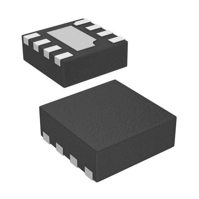
| 产品图片 |
|
| 产品型号 | LTC3412AIUF#PBF |
| PWM类型 | 电流模式,Burst Mode® |
| rohs | 无铅 / 符合限制有害物质指令(RoHS)规范要求 |
| 产品系列 | - |
| 供应商器件封装 | 16-QFN(4x4) |
| 其它名称 | LTC3412AIUFPBF |
| 包装 | 管件 |
| 同步整流器 | 是 |
| 安装类型 | 表面贴装 |
| 封装/外壳 | 16-WQFN 裸露焊盘 |
| 工作温度 | -40°C ~ 125°C |
| 标准包装 | 91 |
| 电压-输入 | 2.25 V ~ 5.5 V |
| 电压-输出 | 0.8 V ~ 5 V |
| 电流-输出 | 3A |
| 类型 | 降压(降压) |
| 输出数 | 1 |
| 输出类型 | 可调式 |
| 频率-开关 | 1MHz |


PDF Datasheet 数据手册内容提取
LTC3412A 3A, 4MHz, Monolithic Synchronous Step-Down Regulator FEATURES DESCRIPTION n High Efficiency: Up to 95% The LTC®3412A is a high efficiency monolithic synchro- n 3A Output Current nous, step-down DC/DC converter utilizing a constant n Low Quiescent Current: 64µA frequency, current mode architecture. It operates from n Low R Internal Switch: 77mΩ an input voltage range of 2.25V to 5.5V and provides a DS(ON) n 2.25V to 5.5V Input Voltage Range regulated output voltage from 0.8V to 5V while deliver- n Programmable Frequency: 300kHz to 4MHz ing up to 3A of output current. The internal synchronous n ±2% Output Voltage Accuracy power switch with 77mΩ on-resistance increases efficiency n 0.8V Reference Allows Low Output Voltage and eliminates the need for an external Schottky diode. n Selectable Forced Continuous/Burst Mode® Operation Switching frequency is set by an external resistor or can with Adjustable Burst Clamp be synchronized to an external clock. 100% duty cycle n Synchronizable Switching Frequency provides low dropout operation extending battery life in n Low Dropout Operation: 100% Duty Cycle portable systems. OPTI-LOOP® compensation allows the n Power Good Output Voltage Monitor transient response to be optimized over a wide range of n Overtemperature Protected loads and output capacitors. n Available in 16-Lead Exposed Pad TSSOP and The LTC3412A can be configured for either Burst Mode QFN Packages operation or forced continuous operation. Forced continu- APPLICATIONS ous operation reduces noise and RF interference while Burst Mode operation provides high efficiency by reducing n Point-of-Load Regulation gate charge losses at light loads. In Burst Mode operation, n Notebook Computers external control of the burst clamp level allows the output n Portable Instruments voltage ripple to be adjusted according to the application n Distributed Power Systems requirements. L, LT, LTC, LTM, Burst Mode, OPTI-LOOP, Linear Technology and the Linear logo are registered trademarks and ThinSOT is a trademark of Analog Devices, Inc. All other trademarks are the property of their respective owners. Protected by U.S. Patents including 5481178, 6580258, 6304066, 6127815, 6498466, 6611131, 6724174. TYPICAL APPLICATION 22µF VIN Efficiency and Power Loss 3.3V 100 100000 PVIN SVIN 95 EFFICIENCY 2.2M RT PGOOD 90 10000 0.47µH 294k LTC3412A SW V2.O5UVT AT 3A %) 85 POW 1000pF 12.1k SRITYUHNNC//SMSODE PSGG VNNFDDB C1×02O0UµTF EFFICIENCY ( 87760505 1100000 ER LOSS (mW) 820pF 60 POWER LOSS 10 69.8k 392k 115k 55 3412A F01a 50 1 0.01 0.1 1 10 LOAD CURRENT (A) Figure 1. 2.5V/3A Step-Down Regulator 3412A F01b 3412aff 1 FFoorr mmoorree iinnffoorrmmaattiioonn wwwwww..lliinneeaarr..ccoomm//LLTTCC33441122AA
LTC3412A ABSOLUTE MAXIMUM RATINGS (Note 1) Input Supply Voltage ....................................–0.3V to 6V Operating Junction Temperature Range (Notes 2, 5) I , RUN/SS, V , PGOOD, E-, I-Grades .......................................–40°C to 125°C TH FB SYNC/MODE Voltages ....................................–0.3 to V MP-Grade ..........................................–55°C to 125°C IN SW Voltages ..................................–0.3V to (V + 0.3V) Storage Temperature Range ....................–65°C to150°C IN Lead Temperature (Soldering, 10 sec) ..................300°C PIN CONFIGURATION TOP VIEW TOP VIEW E D O M SVIN 1 16 PVIN C/ PGOOD 2 15 SW SYN RT VFB ITH ITH 3 14 SW 16 15 14 13 VFB 4 17 13 PGND RUN/SS 1 12 PGOOD RT 5 12 PGND SGND 2 17 11 SVIN SYNC/MODE 6 11 SW PVIN 3 10 PVIN SW 4 9 SW RUN/SS 7 10 SW 5 6 7 8 SGND 8 9 PVIN W D D W FE PACKAGE S PGN PGN S 16-LEAD PLASTIC TSSOP UF PACKAGE TJMAX = 125°C, θJA = 38°C/W, θJC = 10°C/W 16-LEAD (4mm × 4mm) PLASTIC QFN EXPOSED PAD (PIN 17) IS SGND, MUST BE SOLDERED TO PCB TJMAX = 125°C, θJA = 37°C/W, θJC = 5°C/W EXPOSED PAD (PIN 17) IS GND, MUST BE CONNECTED TO PCB ORDER INFORMATION http://www.linear.com/product/LTC3412A#orderinfo LEAD FREE FINISH TAPE AND REEL PART MARKING* PACKAGE DESCRIPTION TEMPERATURE RANGE LTC3412AEFE#PBF LTC3412AEFE#TRPBF 3412AEFE 16-Lead Plastic TSSOP –40°C to 125°C LTC3412AIFE#PBF LTC3412AIFE#TRPBF 3412AIFE 16-Lead Plastic TSSOP –40°C to 125°C LTC3412AEUF#PBF LTC3412AEUF#TRPBF 3412A 16-Lead (4mm × 4mm) Plastic QFN –40°C to 125°C LTC3412AIUF#PBF LTC3412AIUF#TRPBF 3412A 16-Lead (4mm × 4mm) Plastic QFN –40°C to 125°C LEAD BASED FINISH TAPE AND REEL PART MARKING* PACKAGE DESCRIPTION TEMPERATURE RANGE LTC3412AEFE LTC3412AEFE#TR 3412AEFE 16-Lead Plastic TSSOP –40°C to 125°C LTC3412AIFE LTC3412AIFE#TR 3412AIFE 16-Lead Plastic TSSOP –40°C to 125°C LTC3412AMPFE LTC3412AMPFE#TR 3412AMPFE 16-Lead Plastic TSSOP –55°C to 125°C LTC3412AEUF LTC3412AEUF#TR 3412A 16-Lead (4mm × 4mm) Plastic QFN –40°C to 125°C LTC3412AIUF LTC3412AIUF#TR 3412A 16-Lead (4mm × 4mm) Plastic QFN –40°C to 125°C Consult LTC Marketing for parts specified with wider operating temperature ranges. *The temperature grade is identified by a label on the shipping container. For more information on lead free part marking, go to: http://www.linear.com/leadfree/ For more information on tape and reel specifications, go to: http://www.linear.com/tapeandreel/. Some packages are available in 500 unit reels through designated sales channels with #TRMPBF suffix. 3412aff 2 FFoorr mmoorree iinnffoorrmmaattiioonn wwwwww..lliinneeaarr..ccoomm//LLTTCC33441122AA
LTC3412A ELECTRICAL CHARACTERISTICS The l denotes the specifications which apply over the full operating junction temperature range, otherwise specifications are at T ≈ T = 25°C. V = 3.3V unless otherwise specified. A J IN SYMBOL PARAMETER CONDITIONS MIN TYP MAX UNITS SV Signal Input Voltage Range 2.25 5.5 V IN V Regulated Feedback Voltage (Note 3) FB E-, I-Grades l 0.784 0.800 0.816 V MP-Grade l 0.780 0.800 0.816 V I Voltage Feedback Leakage Current 0.1 0.2 µA FB ∆V Reference Voltage Line Regulation V = 2.7V to 5.5V (Note 3) l 0.04 0.2 %V FB IN V Output Voltage Load Regulation Measured in Servo Loop, V = 0.36V l 0.02 0.2 % LOADREG ITH Measured in Servo Loop, V = 0.84V l –0.02 –0.2 % ITH ∆V Power Good Range ±7.5 ±9 % PGOOD R Power Good Pull-Down Resistance 120 200 Ω PGOOD I Input DC Bias Current (Note 4) Q Active Current V = 0.78V, V = 1V 250 330 µA FB ITH Sleep V = 1V, V = 0V 64 80 µA FB ITH Shutdown V = 0V, V = 0V 0.02 1 µA RUN MODE f Switching Frequency R = 294kΩ 0.88 1 1.1 MHz OSC OSC Switching Frequency Range (Note 6) 0.3 4 MHz f SYNC Capture Range (Note 6) 0.3 4 MHz SYNC R R of P-Channel FET I = 1A (Note 7) 77 110 mΩ PFET DS(ON) SW R R of N-Channel FET I = –1A (Note 7) 65 90 mΩ NFET DS(ON) SW I Peak Current Limit 4.5 6 A LIMIT V Undervoltage Lockout Threshold 1.75 2 2.25 V UVLO I SW Leakage Current V = 0V, V = 5.5V 0.1 1 µA LSW RUN IN V RUN Threshold 0.5 0.65 0.8 V RUN I RUN/SS Leakage Current 1 µA RUN Note 1: Stresses beyond those listed under Absolute Maximum Ratings Note 3: The LTC3412A is tested in a feedback loop that adjusts V to FB may cause permanent damage to the device. Exposure to any Absolute achieve a specified error amplifier output voltage (I ). TH Maximum Rating condition for extended periods may affect device Note 4: Dynamic supply current is higher due to the internal gate charge reliability and lifetime. being delivered at the switching frequency. Note 2: The LTC3412AE is guaranteed to meet performance specifications Note 5: T is calculated from the ambient temperature T and power J A from 0°C to 85°C. Specifications over the –40°C to 125°C operating dissipation as follows: LTC3412AFE: T = T + P (38°C/W) J A D junction temperature range are assured by design, characterization and LTC3412AUF: T = T + P (34°C/W) J A D correlation with statistical process controls. The LTC3412AI is guaranteed Note 6: 4MHz operation is guaranteed by design and not production tested. to meet performance specifications over the –40°C to 125°C operating Note 7: Switch on resistance is guaranteed by design and test condition in junction temperature range. The LTC3412AMP is guaranteed and tested to the UF package and by final test correlation in the FE package. meet performance specifications over the full –55°C to 125°C operating junction temperature range. Note that the maximum ambient temperature consistent with these specifications is determined by specific operating conditions in conjunction with board layout, the rated package thermal resistance and other environmental factors. 3412aff 3 FFoorr mmoorree iinnffoorrmmaattiioonn wwwwww..lliinneeaarr..ccoomm//LLTTCC33441122AA
LTC3412A TYPICAL PERFORMANCE CHARACTERISTICS Efficiency vs Load Current, Efficiency vs Load Current, Efficiency vs Load Current Burst Mode Operation Forced Continuous Operation 100 100 100 90 Burst Mode 95 VIN = 3.3V 90 VIN = 3.3V OPERATION 80 90 80 70 85 VIN = 5V 70 VIN = 5V %) FORCED %) %) Y ( 60 CONTINUOUS Y ( 80 Y ( 60 C C C N 50 N 75 N 50 E E E CI CI CI FI 40 FI 70 FI 40 F F F E E E 30 65 30 20 60 20 VIN = 3.3V 10 VOUT = 2.5V 55 VOUT = 2.5V 10 VOUT = 2.5V FIGURE 4 CIRCUIT FIGURE 4 CIRCUIT FIGURE 4 CIRCUIT 0 50 0 0.01 0.1 1 10 0.01 0.1 1 10 0.01 0.1 1 10 LOAD CURRENT (A) LOAD CURRENT (A) LOAD CURRENT (A) 3412A GO1 3412A GO2 3412A GO3 Efficiency vs Input Voltage Efficiency vs Frequency Load Regulation 94 96 0 FIGURE 4 CIRCUIT FIGURE 4 CIRCUIT FIGURE 4 CIRCUIT 95 VIN = 3.3V VIN = 3.3V 92 1µH –0.1 1A 94 0.22µH 90 %) 0.1A %) 93 0.47µH %) –0.2 CIENCY ( 8886 CIENCY ( 9921 /V (UTOUT–0.3 EFFI EFFI 90 ∆VO–0.4 84 3A 89 –0.5 82 88 80 87 –0.6 2.5 3.0 3.5 4.0 4.5 5.0 0 0.5 1.0 1.5 2.0 2.5 3.0 3.5 4.0 0 0.5 1.0 1.5 2.0 2.5 3.0 INPUT VOLTAGE (V) FREQUENCY (MHz) LOAD CURRENT (A) 3412A GO4 3412A GO5 3412A GO6 Load Step Transient Burst Mode Burst Mode Operation Output Voltage Ripple Operation BURST VOUT MODE 20mV/DIV 20mV/DIV VOUT 100mV/DIV PULSE SKIPPING 20mV/DIV INDUCTOR CURRENT FORCED INDUCTOR 1A/DIV CONTINUOUS CURRENT 20mV/DIV 2A/DIV FIGURE 4 CIRCUIT 5µs/DIV VIN = 3.3V 5µs/DIV VIN = 3.3V 40µs/DIV VOUT = 2.5V VOUT = 2.5V FIGURE 4 CIRCUIT F = 1MHz 3412A GO7 3412A GO8 3412A GO9 LOAD STEP = 50mA TO 2A FIGURE 4 CIRCUIT 3412aff 4 FFoorr mmoorree iinnffoorrmmaattiioonn wwwwww..lliinneeaarr..ccoomm//LLTTCC33441122AA
LTC3412A TYPICAL PERFORMANCE CHARACTERISTICS Load Step Transient Forced Continuous Start-Up Transient V vs Temperature REF 0.7975 VIN = 3.3V VOUT 0.7970 2V/DIV VOUT 0.7965 100mV/DIV 0.7960 V)0.7955 R2UVN/D/SISV (REF0.7950 V INDUCTOR 0.7945 CURRENT INDUCTOR 2A/DIV CURRENT 0.7940 2A/DIV 0.7935 0.7930 VIN = 3.3V 40µs/DIV VIN = 3.3V 1ms/DIV –45 –25 –5 15 35 55 75 95 115 VOUT =2.5V VOUT =2.5V TEMPERATURE (°C) f = 1MHz LOAD STEP = 2A 3412A G10 3412A G11 3412A G12 LOAD STEP = 0A TO 3A FIGURE 4 CIRCUIT FIGURE 4 CIRCUIT Switch On-Resistance Switch On-Resistance Switch Leakage Current vs Input Voltage vs Temperature vs Input Voltage 100 120 50 VIN = 3.3V 95 45 90 100 nA) 40 Ω) 85 Ω) NT ( 35 ON-RESISTANCE (m 87760505 PNFFEETT ON-RESISTANCE (m 864000 NPFFEETT CH LEAKAGE CURRE 32210505 PFET T 60 WI 10 20 S 55 5 NFET 50 0 0 2.5 3.0 3.5 4.0 4.5 5.0 –40 –20 0 20 40 60 80 100 120 2.5 3.0 3.5 4.0 4.5 5.0 5.5 INPUT VOLTAGE (V) TEMPERATURE (°C) INPUT VOLTAGE (V) 3412A G13 3412A G14 3412A G15 Frequency vs R Frequency vs Input Voltage Frequency vs Temperature OSC 5000 1060 1020 VIN = 3.3V ROSC = 294k VIN = 3.3V 4500 1050 1015 ROSC = 294k 4000 1010 FREQUENCY (kHz)33221505050000000000 FREQUENCY (kHz)1111000043210000 FREQUENCY (kHz) 11009990099850505 1000 980 1000 500 975 0 990 970 40 140 240 340 440 540 640 740 840 940 2.5 3.0 3.5 4.0 4.5 5.0 5.5 –40 –20 0 20 40 60 80 100 120 ROSC (kΩ) INPUT VOLTAGE (V) TEMPERATURE (°C) 3412A G16 3412A G17 3412A G18 3412aff 5 FFoorr mmoorree iinnffoorrmmaattiioonn wwwwww..lliinneeaarr..ccoomm//LLTTCC33441122AA
LTC3412A TYPICAL PERFORMANCE CHARACTERISTICS Quiescent Current vs Input Voltage Quiescent Current vs Temperature 350 350 VIN = 3.3V 300 ACTIVE 300 ACTIVE A) A) T (µ250 T (µ250 N N E E R200 R200 R R U U C C NT 150 NT 150 E E C C S S QUIE100 SLEEP QUIE100 SLEEP 50 50 0 0 2.5 3.0 3.5 4.0 4.5 5.0 5.5 –40 –20 0 20 40 60 80 100 120 INPUT VOLTAGE (V) TEMPERATURE (°C) 3412A G19 3412A G20 Minimum Peak Inductor Current vs Burst Clamp Voltage Peak Current vs Input Voltage 4000 8.0 A) m T (3500 7.5 R CURREN32050000 RRENT (A) 76..05 O U T C M PEAK INDUC211050000000 AK INDUCTOR 655...050 U E M P XI 500 4.5 A M 0 4.0 0.1 0.2 0.3 0.4 0.5 0.6 0.7 2.25 2.75 3.25 3.75 4.25 4.75 VBURST (V) INPUT VOLTAGE (V) 3412A G21 3412A G22 3412aff 6 FFoorr mmoorree iinnffoorrmmaattiioonn wwwwww..lliinneeaarr..ccoomm//LLTTCC33441122AA
LTC3412A PIN FUNCTIONS (FE/UHF) SV (Pin 1/Pin 11): Signal Input Supply. Decouple this RUN/SS (Pin 7/Pin 1): Run Control and Soft-Start Input. IN pin to SGND with a capacitor. Forcing this pin below 0.5V shuts down the LTC3412A. In shutdown all functions are disabled drawing <1µA of PGOOD (Pin 2/Pin 12): Power Good Output. Open-drain supply current. A capacitor to ground from this pin sets logic output that is pulled to ground when the output volt- the ramp time to full output current. age is not within ±7.5% of regulation point. SGND (Pin 8/Pin 2): Signal Ground. All small-signal com- I (Pin 3/Pin 13): Error Amplifier Compensation Point. TH ponents, compensation components and the exposed pad The current comparator threshold increases with this on the bottom side of the IC should connect to this ground, control voltage. Nominal voltage range for this pin is from which in turn connects to PGND at one point. 0.2V to 1.4V with 0.4V corresponding to the zero-sense voltage (zero current). PV (Pins 9, 16/Pins 3, 10): Power Input Supply. Decouple IN this pin to PGND with a capacitor. V (Pin 4/Pin 14): Feedback Pin. Receives the feedback FB voltage from a resistive divider connected across the SW (Pins 10, 11, 14, 15/Pins 4, 5, 8, 9): Switch Node output. Connection to the Inductor. This pin connects to the drains of the internal main and synchronous power MOSFET R (Pin 5/Pin 15): Oscillator Resistor Input. Connecting T switches. a resistor to ground from this pin sets the switching frequency. PGND (Pins 12, 13/Pins 6, 7): Power Ground. Connect this pin close to the (–) terminal of C and C . SYNC/MODE (Pin 6/Pin 16): Mode Select and External IN OUT Clock Synchronization Input. To select forced continuous, Exposed Pad (Pin 17/Pin 17): Signal Ground. Must be tie to SV . Connecting this pin to a voltage between 0V soldered to PCB for electrical connection and rated thermal IN and 1V selects Burst Mode operation with the burst clamp performance. set to the pin voltage. 3412aff 7 FFoorr mmoorree iinnffoorrmmaattiioonn wwwwww..lliinneeaarr..ccoomm//LLTTCC33441122AA
LTC3412A FUNCTIONAL BLOCK DIAGRAM SVIN SGND ITH PVIN 1 8 3 9 16 VOLTAGE SLOPE PMOS CURRENT REFERENCE COMPENSATION COMPARATOR RECOVERY 0.8V BCLAMP + + – – P-CH VFB 4 – ERROR AMPLIFIER + + BURST SYNC/MODE – COMPARATOR 0.74V + 10 SLOPE 11 – OSCILLATOR COMPENSATION SW 14 15 + RUN/SS 7 RUN N-CH LOGIC 0.86V – + PGOOD 2 – NMOS CURRENT COMPARATOR – + REVERSE 12 CURRENT PGND COMPARATOR 13 5 6 3412 FBD RT SYNC/MODE OPERATION Main Control Loop comparing the feedback signal from a resistor divider on the V pin with an internal 0.8V reference. When the load The LTC3412A is a monolithic, constant-frequency, current FB current increases, it causes a reduction in the feedback mode step-down DC/DC converter. During normal opera- voltage relative to the reference. The error amplifier raises tion, the internal top power switch (P-channel MOSFET) is the I voltage until the average inductor current matches turned on at the beginning of each clock cycle. Current in TH the new load current. When the top power MOSFET shuts the inductor increases until the current comparator trips off, the synchronous power switch (N-channel MOSFET) and turns off the top power MOSFET. The peak inductor turns on until either the bottom current limit is reached or current at which the current comparator shuts off the top the beginning of the next clock cycle. The bottom current power switch is controlled by the voltage on the I pin. TH limit is set at –1.3A for forced continuous mode and 0A The error amplifier adjusts the voltage on the I pin by TH for Burst Mode operation. 3412aff 8 FFoorr mmoorree iinnffoorrmmaattiioonn wwwwww..lliinneeaarr..ccoomm//LLTTCC33441122AA
LTC3412A OPERATION The operating frequency is externally set by an external Pulse-skipping operation is implemented by connecting resistor connected between the R pin and ground. The the SYNC/MODE pin to ground. This forces the burst T practical switching frequency can range from 300kHz to clamp level to be at 0V. As the load current decreases, the 4MHz. peak inductor current will be determined by the voltage on the I pin until the I voltage drops below 400mV. At Overvoltage and undervoltage comparators will pull the TH TH this point, the peak inductor current is determined by the PGOOD output low if the output voltage comes out of minimum on-time of the current comparator. If the load regulation by ±7.5%. In an overvoltage condition, the top demand is less than the average of the minimum on-time power MOSFET is turned off and the bottom power MOSFET inductor current, switching cycles will be skipped to keep is switched on until either the overvoltage condition clears the output voltage in regulation. or the bottom MOSFET’s current limit is reached. Frequency Synchronization Forced Continuous Mode The internal oscillator of the LTC3412A can be synchro- Connecting the SYNC/MODE pin to SV will disable Burst IN nized to an external clock connected to the SYNC/MODE Mode operation and force continuous current operation. pin. The frequency of the external clock can be in the At light loads, forced continuous mode operation is less range of 300kHz to 4MHz. For this application, the oscil- efficient than Burst Mode operation, but may be desirable in lator timing resistor should be chosen to correspond to some applications where it is necessary to keep switching a frequency that is 25% lower than the synchronization harmonics out of a signal band. The output voltage ripple frequency. During synchronization, the burst clamp is set is minimized in this mode. to 0V, and each switching cycle begins at the falling edge of the clock signal. Burst Mode Operation Connecting the SYNC/MODE pin to a voltage in the range Dropout Operation of 0V to 1V enables Burst Mode operation. In Burst Mode When the input supply voltage decreases toward the output operation, the internal power MOSFETs operate intermit- voltage, the duty cycle increases toward the maximum tently at light loads. This increases efficiency by minimiz- on-time. Further reduction of the supply voltage forces ing switching losses. During Burst Mode operation, the the main switch to remain on for more than one cycle minimum peak inductor current is externally set by the eventually reaching 100% duty cycle. The output voltage voltage on the SYNC/MODE pin and the voltage on the I TH will then be determined by the input voltage minus the pin is monitored by the burst comparator to determine voltage drop across the internal P-channel MOSFET and when sleep mode is enabled and disabled. When the the inductor. average inductor current is greater than the load current, the voltage on the I pin drops. As the I voltage falls TH TH Low Supply Operation below 150mV, the burst comparator trips and enables sleep mode. During sleep mode, the top power MOSFET The LTC3412A is designed to operate down to an input is held off and the I pin is disconnected from the output supply voltage of 2.25V. One important consideration at low TH of the error amplifier. The majority of the internal circuitry input supply voltages is that the RDS(ON) of the P-channel is also turned off to reduce the quiescent current to 64µA and N-channel power switches increases. The user should while the load current is solely supplied by the output calculate the power dissipation when the LTC3412A is used capacitor. When the output voltage drops, the I pin is at 100% duty cycle with low input voltages to ensure that TH reconnected to the output of the error amplifier and the thermal limits are not exceeded. top power MOSFET along with all the internal circuitry is switched back on. This process repeats at a rate that is dependent on the load demand. 3412aff 9 FFoorr mmoorree iinnffoorrmmaattiioonn wwwwww..lliinneeaarr..ccoomm//LLTTCC33441122AA
LTC3412A APPLICATIONS INFORMATION Slope Compensation and Inductor Peak Current Although frequencies as high as 4MHz are possible, the minimum on-time of the LTC3412A imposes a minimum Slope compensation provides stability in constant fre- limit on the operating duty cycle. The minimum on-time quency architectures by preventing subharmonic oscilla- is typically 110ns; therefore, the minimum duty cycle is tions at duty cycles greater than 50%. It is accomplished equal to 100 • 110ns • f(Hz). internally by adding a compensating ramp to the inductor current signal at duty cycles in excess of 40%. Normally, Inductor Selection the maximum inductor peak current is reduced when For a given input and output voltage, the inductor value slope compensation is added. In the LTC3412A, however, and operating frequency determine the ripple current. The slope compensation recovery is implemented to keep the ripple current ∆I increases with higher V or V and maximum inductor peak current constant throughout the L IN OUT decreases with higher inductance. range of duty cycles. This keeps the maximum output current relatively constant regardless of duty cycle. ⎛ V ⎞⎛ V ⎞ ΔI = OUT 1– OUT L ⎜ ⎟⎜ ⎟ ⎝ fL ⎠⎝ V ⎠ Short-Circuit Protection IN Having a lower ripple current reduces the core losses in When the output is shorted to ground, the inductor cur- the inductor, the ESR losses in the output capacitors, and rent decays very slowly during a single switching cycle. the output voltage ripple. Highest efficiency operation is To prevent current runaway from occurring, a secondary achieved at low frequency with small ripple current. This, current limit is imposed on the inductor current. If the however, requires a large inductor. inductor valley current increases larger than 4.4A, the top power MOSFET will be held off and switching cycles will A reasonable starting point for selecting the ripple current be skipped until the inductor current is reduced. is ∆I = 0.4(I ). The largest ripple current occurs at the L MAX highest V . To guarantee that the ripple current stays The basic LTC3412A application circuit is shown in Fig- IN below a specified maximum, the inductor value should ure 1. External component selection is determined by the be chosen according to the following equation: maximum load current and begins with the selection of the operating frequency and inductor value followed by ⎛ V ⎞⎛ V ⎞ L= OUT 1– OUT C and C . ⎜ ⎟⎜ ⎟ IN OUT ⎝ fΔIL(MAX)⎠⎝ VIN(MAX)⎠ Operating Frequency The inductor value will also have an effect on Burst Mode Selection of the operating frequency is a trade-off between operation. The transition to low current operation begins efficiency and component size. High frequency operation when the peak inductor current falls below a level set by allows the use of smaller inductor and capacitor values. the burst clamp. Lower inductor values result in higher Operation at lower frequencies improves efficiency by ripple current which causes this to occur at lower load reducing internal gate charge losses but requires larger currents. This causes a dip in efficiency in the upper inductance values and/or capacitance to maintain low range of low current operation. In Burst Mode operation, output ripple voltage. lower inductance values will cause the burst frequency to increase. The operating frequency of the LTC3412A is determined by an external resistor that is connected between pin R T Inductor Core Selection and ground. The value of the resistor sets the ramp current that is used to charge and discharge an internal timing Once the value for L is known, the type of inductor must capacitor within the oscillator and can be calculated by be selected. Actual core loss is independent of core size using the following equation: for a fixed inductor value, but it is very dependent on the inductance selected. As the inductance increases, core 11 3.08(cid:127)10 R = (Ω)–10kΩ losses decrease. Unfortunately, increased inductance OSC f requires more turns of wire and therefore copper losses will increase. 3412aff 10 FFoorr mmoorree iinnffoorrmmaattiioonn wwwwww..lliinneeaarr..ccoomm//LLTTCC33441122AA
LTC3412A APPLICATIONS INFORMATION Ferrite designs have very low core losses and are pre- capacitance that is necessary to ensure that the control ferred at high switching frequencies, so design goals can loop is stable. Loop stability can be checked by viewing concentrate on copper loss and preventing saturation. the load transient response as described in a later section. Ferrite core material saturates “hard,” which means that The output ripple, ∆V , is determined by: OUT inductance collapses abruptly when the peak design current ⎛ 1 ⎞ is exceeded. This results in an abrupt increase in inductor ΔV ≤ΔI ESR+ OUT L⎜ ⎟ ripple current and consequent output voltage ripple. Do ⎝ 8fCOUT⎠ not allow the core to saturate! The output ripple is highest at maximum input voltage Different core materials and shapes will change the size/cur- since ∆I increases with input voltage. Multiple capacitors L rent and price/current relationship of an inductor. Toroid placed in parallel may be needed to meet the ESR and or shielded pot cores in ferrite or permalloy materials are RMS current handling requirements. Dry tantalum, special small and don’t radiate much energy, but generally cost polymer, aluminum electrolytic, and ceramic capacitors are more than powdered iron core inductors with similar all available in surface mount packages. Special polymer characteristics. The choice of which style inductor to use capacitors offer very low ESR but have lower capacitance mainly depends on the price verus size requirements and density than other types. Tantalum capacitors have the any radiated field/EMI requirements. New designs for highest capacitance density but it is important to only surface mount inductors are available from Coiltronics, use types that have been surge tested for use in switching Coilcraft, Toko and Sumida. power supplies. Aluminum electrolytic capacitors have significantly higher ESR, but can be used in cost-sensitive C and C Selection IN OUT applications provided that consideration is given to ripple The input capacitance, C , is needed to filter the trapezoidal current ratings and long-term reliability. Ceramic capacitors IN wave current at the source of the top MOSFET. To prevent have excellent low ESR characteristics but can have a high large voltage transients from occurring, a low ESR input voltage coefficient and audible piezoelectric effects. The capacitor sized for the maximum RMS current should be high Q of ceramic capacitors with trace inductance can used. The maximum RMS current is given by: also lead to significant ringing. V V Using Ceramic Input and Output Capacitors I =I OUT IN –1 RMS OUT(MAX) V V IN OUT Higher values, lower cost ceramic capacitors are now becoming available in smaller case sizes. Their high ripple This formula has a maximum at V = 2V , where IN OUT current, high voltage rating and low ESR make them ideal I = I . This simple worst-case condition is com- RMS OUT/2 for switching regulator applications. However, care must monly used for design because even significant deviations be taken when these capacitors are used at the input and do not offer much relief. Note that ripple current ratings output. When a ceramic capacitor is used at the input and from capacitor manufacturers are often based on only the power is supplied by a wall adapter through long wires, 2000 hours of life which makes it advisable to further a load step at the output can induce ringing at the input, derate the capacitor, or choose a capacitor rated at a higher V . At best, this ringing can couple to the output and be temperature than required. Several capacitors may also IN mistaken as loop instability. At worst, a sudden inrush be paralleled to meet size or height requirements in the of current through the long wires can potentially cause a design. For low input voltage applications, sufficient bulk voltage spike at V large enough to damage the part. input capacitance is needed to minimize transient effects IN during output load changes. When choosing the input and output ceramic capacitors, choose the X5R or X7R dielectric formulations. These The selection of C is determined by the effective series OUT dielectrics have the best temperature and voltage charac- resistance (ESR) that is required to minimize voltage ripple teristics of all the ceramics for a given value and size. and load step transients as well as the amount of bulk 3412aff 11 FFoorr mmoorree iinnffoorrmmaattiioonn wwwwww..lliinneeaarr..ccoomm//LLTTCC33441122AA
LTC3412A APPLICATIONS INFORMATION Output Voltage Programming The value for I is determined by the desired amount BURST of output voltage ripple. As the value of I increases, The output voltage is set by an external resistive divider BURST the sleep period between pulses and the output voltage according to the following equation: ripple increase. The burst clamp voltage, V , can be BURST ⎛ R2⎞ set by a resistor divider from the V pin to the SGND pin V =0.8V 1+ FB OUT ⎝⎜ R1⎠⎟ as shown in Figure 1. Pulse skipping, which is a compromise between low out- The resistive divider allows pin V to sense a fraction of FB put voltage ripple and efficiency, can be implemented by the output voltage as shown in Figure 2. connecting pin SYNC/MODEto ground. This sets I to BURST 0A. In this condition, the peak inductor current is limited VOUT by the minimum on-time of the current comparator. The R2 lowest output voltage ripple is achieved while still operat- ing discontinuously. During very light output loads, pulse VFB skipping allows only a few switching cycles to be skipped LTC3412A R1 while maintaining the output voltage in regulation. SGND Frequency Synchronization 3412A F02 Figure 2. Setting the Output Voltage The LTC3412A’s internal oscillator can be synchronized to an external clock signal. During synchronization, the Burst Clamp Programming top MOSFET turn-on is locked to the falling edge of the If the voltage on the SYNC/MODE pin is less than V by external frequency source. The synchronization frequency IN 1V, Burst Mode operation is enabled. During Burst Mode range is 300kHz to 4MHz. Synchronization only occurs if Operation, the voltage on the SYNC/MODE pin determines the external frequency is greater than the frequency set the burst clamp level, which sets the minimum peak by the external resistor. Because slope compensation inductor current, I . To select the burst clamp level, is generated by the oscillator’s RC circuit, the external BURST use the graph of Minimum Peak Inductor Current vs Burst frequency should be set 25% higher than the frequency Clamp Voltage in the Typical Performance Characteristics set by the external resistor to ensure that adequate slope section. compensation is present. V is the voltage on the SYNC/MODE pin. I BURST BURST Soft-Start can only be programmed in the range of 0A to 6A. For The RUN/SS pin provides a means to shut down the values of V greater than 1V, I is set at 6A. For BURST BURST LTC3412A as well as a timer for soft-start. Pulling the values of V less than 0.4V, I is set at 0A. As BURST BURST RUN/SS pin below 0.5V places the LTC3412A in a low the output load current drops, the peak inductor currents quiescent current shutdown state (I < 1µA). decrease to keep the output voltage in regulation. When Q the output load current demands a peak inductor current The LTC3412A contains an internal soft-start clamp that that is less than IBURST, the burst clamp will force the peak gradually raises the clamp on ITH after the RUN/SS pin is inductor current to remain equal to IBURST regardless of pulled above 2V. The full current range becomes available further reductions in the load current. Since the average on I after 1024 switching cycles. If a longer soft-start TH inductor current is greater than the output load current, period is desired, the clamp on I can be set externally TH the voltage on the ITH pin will decrease. When the ITH with a resistor and capacitor on the RUN/SS pin as shown voltage drops to 150mV, sleep mode is enabled in which in Figure 1. The soft-start duration can be calculated by both power MOSFETs are shut off along with most of the using the following formula: circuitry to minimize power consumption. All circuitry is ⎛ V ⎞ turned back on and the power MOSFETs begin switching t =R C ln IN (SECONDS) SS SS SS ⎜ ⎟ again when the output voltage drops out of regulation. ⎝ V –1.8V⎠ IN 3412aff 12 FFoorr mmoorree iinnffoorrmmaattiioonn wwwwww..lliinneeaarr..ccoomm//LLTTCC33441122AA
LTC3412A APPLICATIONS INFORMATION Efficiency Considerations The R for both the top and bottom MOSFETs can be DS(ON) obtained from the Typical Performance Characteristics The efficiency of a switching regulator is equal to the output curves. To obtain I2R losses, simply add R to R and mul- power divided by the input power times 100%. It is often SW L tiply the result by the square of the average output current. useful to analyze individual losses to determine what is limiting the efficiency and which change would produce Other losses including C and C ESR dissipative losses IN OUT the most improvement. Efficiency can be expressed as: and inductor core losses generally account for less than 2% of the total loss. Efficiency = 100% – (L1 + L2 + L3 + ...) where L1, L2, etc. are the individual losses as a percent- Thermal Considerations age of input power. In most applications, the LTC3412A does not dissipate Although all dissipative elements in the circuit produce much heat due to its high efficiency. losses, two main sources usually account for most of the However, in applications where the LTC3412A is running losses: V quiescent current and I2R losses. IN at high ambient temperature with low supply voltage and The VIN quiescent current loss dominates the efficiency loss high duty cycles, such as in dropout, the heat dissipated at very low load currents whereas the I2R loss dominates may exceed the maximum junction temperature of the part. the efficiency loss at medium to high load currents. In a If the junction temperature reaches approximately 150°C, typical efficiency plot, the efficiency curve at very low load both power switches will be turned off and the SW node currents can be misleading since the actual power lost is will become high impedance. of no consequence. To avoid the LTC3412A from exceeding the maximum junc- 1. The V quiescent current is due to two components: the IN tion temperature, the user will need to do some thermal DC bias current as given in the electrical characteristics analysis. The goal of the thermal analysis is to determine and the internal main switch and synchronous switch whether the power dissipated exceeds the maximum junction gate charge currents. The gate charge current results temperature of the part. The temperature rise is given by: from switching the gate capacitance of the internal power t = (P )(θ ) MOSFET switches. Each time the gate is switched from r D JA high to low to high again, a packet of charge dQ moves where P is the power dissipated by the regulator and θ D JA from V to ground. The resulting dQ/dt is the current is the thermal resistance from the junction of the die to IN out of V that is typically larger than the DC bias cur- the ambient temperature. For the 16-lead exposed TSSOP IN rent. In continuous mode, IGATECHG = f(QT + QB) where package, the θJA is 38°C/W. For the 16-lead QFN package QT and QB are the gate charges of the internal top and the θJA is 34°C/W. bottom switches. Both the DC bias and gate charge The junction temperature, T , is given by: J losses are proportional to V ; thus, their effects will IN T = T + t be more pronounced at higher supply voltages. J A r 2. I2R losses are calculated from the resistances of the where TA is the ambient temperature. internal switches, RSW, and external inductor RL. In Note that at higher supply voltages, the junction tempera- continuous mode the average output current flowing ture is lower due to reduced switch resistance (R ). DS(ON) through inductor L is “chopped” between the main To maximize the thermal performance of the LTC3412A, switch and the synchronous switch. Thus, the series the Exposed Pad should be soldered to a ground plane. resistance looking into the SW pin is a function of both top and bottom MOSFET R and the duty cycle Checking Transient Response DS(ON) (DC) as follows: The regulator loop response can be checked by looking R = (R TOP)(DC) + (R BOT)(1 – DC) at the load transient response. Switching regulators take SW DS(ON) DS(ON) several cycles to respond to a step in load current. 3412aff 13 FFoorr mmoorree iinnffoorrmmaattiioonn wwwwww..lliinneeaarr..ccoomm//LLTTCC33441122AA
LTC3412A APPLICATIONS INFORMATION When a load step occurs, V immediately shifts by an Decoupling the PV and SV pins with two 22µF capaci- OUT IN IN amount equal to ∆I , where ESR is the effective tors is adequate for most applications. LOAD(ESR) series resistance of COUT. ∆ILOAD also begins to charge or The burst clamp and output voltage can now be pro- discharge C generating a feedback error signal used by OUT grammed by choosing the values of R1, R2 and R3. The the regulator to return V to its steady-state value. During OUT voltage on pin MODE will be set to 0.50V by the resistor this recovery time, VOUT can be monitored for overshoot divider consisting of R2 and R3. According to the graph or ringing that would indicate a stability problem. The ITH of Minimum Peak Inductor Current vs Burst Clamp Volt- pin external components and output capacitor shown in age in the Typical Performance Characteristics section, a Figure 1 will provide adequate compensation for most burst clamp voltage of 0.5V will set the minimum inductor applications. current, I , to approximately 1.1A. BURST Design Example If we set the sum of R2 and R3 to 185k, then the following equations can be solved: As a design example, consider using the LTC3412A in an application with the following specifications: R2+R3=185k V = 3.3V, V = 2.5V, I = 3A, R2 0.8V IN OUT OUT(MAX) 1+ = IOUT(MIN) = 100mA, f = 1MHz. R3 0.50V Because efficiency is important at both high and low load The two equations shown above result in the following current, Burst Mode operation will be utilized. values for R2 and R3: R2 = 69.8k , R3 = 115k. The value of R1 can now be determined by solving the following First, calculate the timing resistor: equation. 3.08(cid:127)1011 R1 2.5V ROSC = –10k =298k 1+ = 1(cid:127)106 185k 0.8V R1=392k Use a standard value of 294k. Next, calculate the inductor value for about 40% ripple current at maximum VIN: A value of 392k will be selected for R1. Figure 4 shows the complete schematic for this design example. ⎛ 2.5V ⎞⎛ 2.5V⎞ L= 1– =0.51µH ⎜ ⎟⎜ ⎟ ⎝(1MHz)(1.2A)⎠⎝ 3.3V⎠ PC Board Layout Checklist When laying out the printed circuit board, the following Using a 0.47µH inductor results in a maximum ripple checklist should be used to ensure proper operation of current of: the LTC3412A. Check the following in your layout: ⎛ 2.5V ⎞⎛ 2.5V⎞ ΔI = 1– =1.29A 1. A ground plane is recommended. If a ground plane layer L ⎜ ⎟⎜ ⎟ ⎝(1MHz)(0.47µH)⎠⎝ 3.3V⎠ is not used, the signal and power grounds should be segregated with all small signal components returning C will be selected based on the ESR that is required to OUT to the SGND pin at one point which is then connected satisfy the output voltage ripple requirement and the bulk to the PGND pin close to the LTC3412A. capacitance needed for loop stability. For this design, two 100µF ceramic capacitors will be used. 2. Connect the (+) terminal of the input capacitor(s), C , as IN C should be sized for a maximum current rating of: close as possible to the PV pin. This capacitor provides IN IN the AC current into the internal power MOSFETs. ⎛2.5V⎞ 3.3V I =(3A) –1=1.29A RMS ⎜ ⎟ RMS ⎝3.3V⎠ 2.5V 3412aff 14 FFoorr mmoorree iinnffoorrmmaattiioonn wwwwww..lliinneeaarr..ccoomm//LLTTCC33441122AA
LTC3412A APPLICATIONS INFORMATION 3. Keep the switching node, SW, away from all sensitive 5. Connect the V pin directly to the feedback resistors. FB small-signal nodes. The resistor divider must be connected between V OUT and SGND. 4. Flood all unused areas on all layers with copper. Flooding with copper will reduce the temperature rise of power components. You can connect the copper areas to any DC net (PV , SV , V , PGND, SGND, or any other IN IN OUT DC rail in your system). Top Bottom Figure 3. LTC3412A Layout Diagram VIN 3.3V CFF 22pF X5R R1 392k CIN3** 100µF 1 16 SVIN PVIN RPG CIN1 100k 22µF 2 15 PGOOD PGOOD SW CITH 330pF X7R RITH 17.4k 3 14 ITH SW CC LTC3412A 47pF 4 VFB EFE PGND 13 0 . 4L71µ*H 2V.O5UVT 1R153k 69R.28k 5 PGND 12 3A RT ROSC SYNC/MODE SW 11 RSS 294k 6 2.2M 7 10 COUT** RUN SW 100µF CSS ×2 1000pF X7R 8 9 SGND PVIN CIN2 22µF GND X5R 6.3V *VISHAY IHLP-2525CZ-01 3412 F04 **TDK 4532X5R0J107M Figure 4. 3.3V to 2.5V, 3A Regulator at 1MHz, Burst Mode Operation 3412aff 15 FFoorr mmoorree iinnffoorrmmaattiioonn wwwwww..lliinneeaarr..ccoomm//LLTTCC33441122AA
LTC3412A TYPICAL APPLICATIONS 1.2V, 3A, 1.5MHz 1mm Height Regulator Using All Ceramic Capacitors VIN 3.3V C1 22pF X5R R1 95.3k 11 10 RPG SVIN PVIN C10INµ1F 100k 12 9 X5R 6.3V PGOOD PGOOD SW CITH 1000pF X7R 6R.3IT4Hk 13 8 ITH SW CC LTC3412A 22pF 14 VFB EUF PGND 7 0 . 4L71µ*H V1.O2UVT 1R872k 15 PGND 6 3A RT RSS R19O6SkC 16 SYNC/MODE SW 5 COUT** 2.2M 1 4 22µF RUN SW X3 CSS 1000pF X7R2 3 SGND PVIN CIN2 10µF GND X5R 6.3V *COOPER SD10-R47 3412 TA01 **TAIYO YUDEN AMK212BJ226MD-B 1.8V, 3A Step-Down Regulator at 1MHz, Burst Mode Operation VIN C1 47pF X5R 2.5V CIN3** 100µF R1 232k 1 16 SVIN PVIN CIN1 RPG 22µF 100k 2 15 X5R 6.3V PGOOD PGOOD SW CITH 820pF X7R RITH 15k 3 14 C2 ITH SW 47pF 4 LTCE3F4E12A PGND 13 0.4L71µH* VOUT VFB 1.8V 1R153k 69R.28k 5 PGND 12 3A RT R29O4SkC 6 SW 11 COUT** RSS SYNC/MODE 100µF 2.2M 7 10 ×3 RUN SW CSS 1000pF X7R8 9 SGND PVIN CIN2 22µF X5R 6.3V GND 3412 TA02 *VISHAY IHLP-2525CZ-01 **TDK C4532X5R0J107M 3412aff 16 FFoorr mmoorree iinnffoorrmmaattiioonn wwwwww..lliinneeaarr..ccoomm//LLTTCC33441122AA
LTC3412A TYPICAL APPLICATIONS 3.3V, 3A Step-Down Regulator at 2MHz, Forced Continuous Mode Operation VIN CIN3** 5V C1 22pF X5R 100µF R1 634k 1 16 SVIN PVIN RPG C22INµ1F 100k 2 15 X5R 6.3V PGOOD PGOOD SW CITH 820pF X7R RITH 7.5k 3 14 ITH SW CC LTC3412A 47pF 4 VFB EFE PGND 13 0 . 4L71µ*H V3.O3UVT 2R002k 5 PGND 12 3A RT R13O7SkC 6 SYNC/MODE SW 11 COUT** 100µF 7 10 RUN SW ×2 RSS CSS 2.2M 1000pF X7R8 9 SGND PVIN CIN2 22µF GND X5R 6.3V 3412 TA03 *VISHAY IHLP-2525CZ-01 **TDK C4532X5R0J107M 2.5V, 3A Step-Down Regulator Synchronized to 1.8MHz VIN 3.3V C1 22pF X5R R1 392k 1 16 SVIN PVIN RPG C22INµ1F 100k 2 15 X5R 6.3V PGOOD PGOOD SW CITH 220pF X7R RITH 6.49k 3 14 ITH SW CC 22pF 4 LTCE3F4E12A PGND 13 0 . 4L71µ*H VOUT VFB 1.5V R2 162k PGND 12 3A 5 RT ROSC 182k SW 11 + RSS 1.8MHz 6 SYNC/MODE COUT** 2.2M EXT CLOCK 7 10 150µF RUN SW CSS 1000pF X7R8 9 SGND PVIN CIN2 22µF GND X5R 6.3V *COOPER SD20-R47 3412 TA04 **SANYO POSCAP 4TPE150MAZB 3412aff 17 FFoorr mmoorree iinnffoorrmmaattiioonn wwwwww..lliinneeaarr..ccoomm//LLTTCC33441122AA
LTC3412A PACKAGE DESCRIPTION Please refer to http://www.linear.com/product/LTC3412A#packaging for the most recent package drawings. FE Package 16-Lead Plastic TSSOP (4.4mm) (Reference LTC DWG # 05-08-1663 Rev L) Exposed Pad Variation BA 4.90 – 5.10* 2.74 (.193 – .201) (.108) 2.74 (.108) 16 151413121110 9 6.60 ±0.10 2.74 4.50 ±0.10 (.108) SEE NOTE 4 2.74 6.40 (.108) (.252) 0.45 ±0.05 BSC 1.05 ±0.10 0.65 BSC RECOMMENDED SOLDER PAD LAYOUT 1 2 3 4 5 6 7 8 1.10 4.30 – 4.50* (.0433) (.169 – .177) 0.25 MAX REF 0° – 8° 0.65 0.09 – 0.20 0.50 – 0.75 (.0256) 0.05 – 0.15 (.0035 – .0079) (.020 – .030) BSC (.002 – .006) 0.195 – 0.30 (.0077 – .0118) FE16 (BA) TSSOP REV L 0117 NOTE: TYP 1. CONTROLLING DIMENSION: MILLIMETERS 4. RECOMMENDED MINIMUM PCB METAL SIZE MILLIMETERS FOR EXPOSED PAD ATTACHMENT 2. DIMENSIONS ARE IN (INCHES) *DIMENSIONS DO NOT INCLUDE MOLD FLASH. MOLD FLASH 3. DRAWING NOT TO SCALE SHALL NOT EXCEED 0.150mm (.006") PER SIDE UF Package 16-Lead Plastic QFN (4mm × 4mm) (Reference LTC DWG # 05-08-1692 Rev Ø) BOTTOM VIEW—EXPOSED PAD PIN 1 NOTCH R = 0.20 TYP 4.00 ±0.10 0.75 ±0.05 R = 0.115 OR 0.35 × 45° CHAMFER (4 SIDES) TYP 15 16 0.72 ±0.05 PIN 1 0.55 ±0.20 TOP MARK (NOTE 6) 1 2 4.35 ±0.05 2.15 ±0.05 2.15 ±0.10 2.90 ±0.05 (4 SIDES) (4-SIDES) PACKAGE OUTLINE (UF16) QFN 10-04 0.30 ±0.05 0.200 REF 0.30 ±0.05 0.65 BSC 0.00 – 0.05 0.65 BSC RECOMMENDED SOLDER PAD PITCH AND DIMENSIONS NOTE: 1. DRAWING CONFORMS TO JEDEC PACKAGE OUTLINE MO-220 VARIATION (WGGC) 2. DRAWING NOT TO SCALE 3. ALL DIMENSIONS ARE IN MILLIMETERS 4. DIMENSIONS OF EXPOSED PAD ON BOTTOM OF PACKAGE DO NOT INCLUDE MOLD FLASH. MOLD FLASH, IF PRESENT, SHALL NOT EXCEED 0.15mm ON ANY SIDE 5. EXPOSED PAD SHALL BE SOLDER PLATED 6. SHADED AREA IS ONLY A REFERENCE FOR PIN 1 LOCATION ON THE TOP AND BOTTOM OF PACKAGE 3412aff 18 FFoorr mmoorree iinnffoorrmmaattiioonn wwwwww..lliinneeaarr..ccoomm//LLTTCC33441122AA
LTC3412A REVISION HISTORY (Revision history begins at Rev E) REV DATE DESCRIPTION PAGE NUMBER E 03/10 Changed Temperature Range for E- and I-Grades to –40°C to 125°C in Absolute Maximum Ratings and Order 2 Information Sections Changed from T = 25°C to T ≈ T = 25°C in the Electrical Characteristics Heading 3 A A J Updated Note 2 3 F 05/17 Add Storage Temperature to Absolute Maximum Ratings 2 3412aff Information furnished by Linear Technology Corporation is believed to be accurate and reliable. 19 However, no responsibility is assumed for its use. Linear Technology Corporation makes no representa- tion that the interconnFFeoocrrti ommn ooofrr eeits ii nnciffroocurrmmitsaa attsiioo dnnes wwcrwwibwwed.. llhiinnereeeaainrr ..wccioollmm no//tLL inTTfCCri33ng44e11 o22nAA existing patent rights.
LTC3412A RELATED PARTS PART NUMBER DESCRIPTION COMMENTS LTC1878 600mA (I ), 550kHz, Synchronous Step-Down DC/DC Converter 96% Efficiency, V : 2.7V to 6V, V = 0.8V, I = 10µA OUT IN OUT(MIN) Q I <1µA, MS8 Package SD LTC1879 1.20A (I ), 550kHz, Synchronous Step-Down DC/DC Converter 95% Efficiency, V : 2.7V to 10V, V = 0.8V, I = 15µA, OUT IN OUT(MIN) Q I <1µA, TSSOP16 Package SD LT1934/LT1934-1 300mA (I ), Constant Off-Time, High Efficiency Step-Down 90% Efficiency, V : 3.2V to 34V, V = 1.25V, I = 14µA, OUT IN OUT(MIN) Q DC/DC Converter I <1µA, ThinSOT™ Package SD LTC3404 600mA (I ), 1.4MHz, Synchronous Step-Down DC/DC Converter 95% Efficiency, V : 2.7V to 6V, V = 0.8V, I = 10µA, OUT IN OUT(MIN) Q I <1µA, MS8 Package SD LTC3405/LTC3405A 300mA (I ), 1.5MHz, Synchronous Step-Down DC/DC Converter 95% Efficiency, V : 2.5V to 5.5V, V = 0.8V, I = 20µA, OUT IN OUT(MIN) Q I <1µA, ThinSOT Package SD LTC3406/LTC3406B 600mA (I ), 1.5MHz, Synchronous Step-Down DC/DC Converter 96% Efficiency, V : 2.5V to 5.5V, V = 0.6V, I = 20µA, OUT IN OUT(MIN) Q I <1µA, ThinSOT Package SD LTC3407 Dual 600mA (I ), 1.5MHz, Synchronous Step-Down 95% Efficiency, V : 2.5V to 5.5V, V = 0.6V, I = 40µA, OUT IN OUT(MIN) Q DC/DC Converter ISD <1µA, MS10E and 3mm × 3mm DFN Packages LTC3411 1.25A (I ), 4MHz, Synchronous Step-Down DC/DC Converter 95% Efficiency, V : 2.5V to 5.5V, V = 0.8V, I = 60µA, OUT IN OUT(MIN) Q ISD <1µA, MS10 and 3mm × 3mm DFN Packages LTC3412 2.5A (I ), 4MHz, Synchronous Step-Down DC/DC Converter 95% Efficiency, V : 2.5V to 5.5V, V = 0.8V, I = 60µA, OUT IN OUT(MIN) Q I <1µA, TSSOP16E Package SD LTC3413 3A (I Sink/Source), 2MHz, Monolithic Synchronous Regulator 90% Efficiency, V : 2.25V to 5.5V, V = V , OUT IN OUT(MIN) REF/2 for DDR/QDR Memory Termination I = 280µA, I <1µA, TSSOP16E Package Q SD LTC3414 4A (I ), 4MHz, Synchronous Step-Down DC/DC Converter 95% Efficiency, V : 2.25V to 5.5V, V = 0.8V, I = OUT IN OUT(MIN) Q 64µA, I <1µA, TSSOP20E Package SD LTC3416 4A (I ), 4MHz, Synchronous Step-Down DC/DC Converter 95% Efficiency, V : 2.25V to 5.5V, V = 0.8V, I = OUT IN OUT(MIN) Q 64µA, I <1µA, TSSOP20E Package SD LTC3418 8A (I ), 4MHz, Synchronous Step-Down DC/DC Converter 95% Efficiency, V : 2.25V to 5.5V, V = 0.8V, I = OUT IN OUT(MIN) Q 380µA, I <1µA, QFN Package SD LT3430 60V, 2.75A (I ), 200kHz, High Efficiency Step-Down 90% Efficiency, V : 5.5V to 60V, V = 1.20V, I = OUT IN OUT(MIN) Q DC/DC Converter 2.5mA, I 25µA, TSSOP16E Package SD LTC3440 600mA (I ), 2MHz, Synchronous Buck-Boost DC/DC Converter 95% Efficiency, V : 2.5V to 5.5V, V : 2.5V to 5.5V, I = OUT IN OUT Q 25µA, I <1µA, DFN Package SD LTC3441 1.2A (I ), 1MHz, Synchronous Buck-Boost DC/DC Converter 95% Efficiency, V : 2.4V to 5.5V, V : 2.4V to 5.25V, I = OUT IN OUT Q 25µA, I <1µA, DFN Package SD LTC3548 400mA/800mA Dual Synchronous Step-Down DC/DC Converter 95% Efficiency, V : 2.5V to 5.5V, V = 0.6V, I <40µA, IN OUT(MIN) Q I <1µA, MS8E and DFN Packages SD 3412aff 20 LT 0517 REV F • PRINTED IN USA www.linear.com/LTC3412A FFoorr mmoorree iinnffoorrmmaattiioonn wwwwww..lliinneeaarr..ccoomm//LLTTCC33441122AA LINEAR TECHNOLOGY CORPORATION 2005