ICGOO在线商城 > 集成电路(IC) > PMIC - 监控器 > TPS3837J25DBVT

 Datasheet下载
- 型号: TPS3837J25DBVT
- 制造商: Texas Instruments
- 库位|库存: xxxx|xxxx
- 要求:
| 数量阶梯 | 香港交货 | 国内含税 |
| +xxxx | $xxxx | ¥xxxx |
查看当月历史价格
查看今年历史价格
TPS3837J25DBVT产品简介:
ICGOO电子元器件商城为您提供TPS3837J25DBVT由Texas Instruments设计生产,在icgoo商城现货销售,并且可以通过原厂、代理商等渠道进行代购。 TPS3837J25DBVT价格参考¥8.37-¥15.22。Texas InstrumentsTPS3837J25DBVT封装/规格:PMIC - 监控器, 推挽式,图腾柱 监控器 1 通道 SOT-23-5。您可以下载TPS3837J25DBVT参考资料、Datasheet数据手册功能说明书,资料中有TPS3837J25DBVT 详细功能的应用电路图电压和使用方法及教程。
TPS3837J25DBVT 是 Texas Instruments(德州仪器)生产的一款 PMIC - 监控器芯片,属于电压监控器系列。该型号的主要应用场景包括:

1. 电源监控与管理
   TPS3837J25DBVT 用于监控系统电源电压,确保其在正常范围内运行。当检测到电压低于预设阈值(如 2.5V)时,会触发复位信号以保护系统硬件和数据完整性。适用于需要稳定电压的电子设备。

2. 嵌入式系统
   在微控制器或 DSP 系统中,该芯片可以提供可靠的复位功能,确保设备在上电、掉电或电压波动时能够安全启动或重启。例如,在工业控制、家用电器和消费电子产品中广泛应用。

3. 通信设备
   适用于路由器、交换机、基站等通信设备,保障其供电稳定性,避免因电压异常导致的数据丢失或系统故障。

4. 汽车电子
   在汽车电子控制系统中,TPS3837J25DBVT 可用于监控电池电压或辅助电源状态,确保车载信息娱乐系统、发动机控制单元(ECU)等关键模块的安全运行。

5. 便携式设备
   如平板电脑、智能手机和可穿戴设备,TPS3837J25DBVT 能够有效监测电池电压并触发保护机制,延长设备寿命。

6. 医疗设备
   在医疗监护仪、血糖仪等对电源要求较高的设备中,该芯片可提供精准的电压监控功能,确保设备的可靠性和安全性。

7. 工业自动化
   在 PLC(可编程逻辑控制器)、传感器和执行器中,TPS3837J25DBVT 提供稳定的电源监控解决方案,防止因电压波动引起的系统错误。

总之,TPS3837J25DBVT 凭借其高精度的电压检测和快速响应能力,广泛应用于各类需要电源监控的场景,为系统的稳定性和可靠性提供保障。
| 参数 | 数值 |
| 产品目录 | 集成电路 (IC) |
| 描述 | IC 2.25V NANOPWR MON SOT-23-5 |
| 产品分类 | |
| 品牌 | Texas Instruments |
| 数据手册 | |
| 产品图片 |
|
| 产品型号 | TPS3837J25DBVT |
| PCN设计/规格 | |
| rohs | 无铅 / 符合限制有害物质指令(RoHS)规范要求 |
| 产品系列 | - |
| 产品目录页面 | |
| 供应商器件封装 | SOT-23-5 |
| 其它名称 | 296-3344-1 |
| 包装 | 剪切带 (CT) |
| 受监控电压数 | 1 |
| 复位 | 高有效 |
| 复位超时 | 最小为 100 ms |
| 安装类型 | 表面贴装 |
| 封装/外壳 | SC-74A,SOT-753 |
| 工作温度 | -40°C ~ 85°C |
| 标准包装 | 1 |
| 电压-阈值 | 2.25V |
| 类型 | 简单复位/加电复位 |
| 输出 | 推挽式,图腾柱 |


- 商务部:美国ITC正式对集成电路等产品启动337调查
- 曝三星4nm工艺存在良率问题 高通将骁龙8 Gen1或转产台积电
- 太阳诱电将投资9.5亿元在常州建新厂生产MLCC 预计2023年完工
- 英特尔发布欧洲新工厂建设计划 深化IDM 2.0 战略
- 台积电先进制程称霸业界 有大客户加持明年业绩稳了
- 达到5530亿美元!SIA预计今年全球半导体销售额将创下新高
- 英特尔拟将自动驾驶子公司Mobileye上市 估值或超500亿美元
- 三星加码芯片和SET,合并消费电子和移动部门,撤换高东真等 CEO
- 三星电子宣布重大人事变动 还合并消费电子和移动部门
- 海关总署:前11个月进口集成电路产品价值2.52万亿元 增长14.8%


PDF Datasheet 数据手册内容提取
Product Order Technical Tools & Support & Folder Now Documents Software Community TPS3836,TPS3837,TPS3838 SLVS292F–JUNE2000–REVISEDSEPTEMBER2019 TPS383x Nano Power Voltage Supervisor With Selectable Reset Delay 1 Features 3 Description • Supplycurrent:220nA(typical) The TPS3836, TPS3837, and TPS3838 device 1 families of supervisory circuits provide circuit • Precisionsupplyvoltagesupervisionrange: initialization and timing supervision, primarily for 1.8V,2.5V,3.0V,and3.3V digital signal processors (DSP) and processor-based • Power-onresetgeneratorwithselectabledelay systems. time:10msor200ms During power-on, RESET is asserted when the • PushandpullRESEToutput(TPS3836), supply voltage V becomes higher than 1.1 V. DD PushandpullRESEToutput(TPS3837),oropen- Thereafter, the supervisory circuit monitors V and DD drainRESEToutput(TPS3838) keeps the RESET output active as long as V DD • Manualreset remains below the threshold voltage of VIT. An internal timer delays the return of the output to the • 5-pinSOT23and2-mm×2-mm,6-pinSON inactive state (high) to ensure proper system reset. packages The delay time starts after V rises above the DD • Temperaturerange:–40°Cto85°C thresholdvoltageV . IT When CT is connected to GND, a fixed delay time of 2 Applications typically 10 ms is asserted. When connected to V , DD • Applicationsusinglow-powerDSPs, the delay time is typically 200 ms. When the supply microcontrollers,ormicroprocessors voltage drops below the threshold voltage VIT, the output becomes active (low) again. All the devices of • Portable-andbattery-poweredequipment this family have a fixed-sense threshold voltage (V ) IT • Intelligentinstruments setbyaninternalvoltagedivider. • Wirelesscommunicationsystems The TPS3836 has an active-low, push-pull RESET • Notebookcomputers output. The TPS3837 has an active-high, push-pull • Applicationsusingthe MSP430™ RESET, and the TPS3838 integrates an active-low, open-drain RESET output. The product spectrum is • Forautomotivesystems,seeTPS383x-Q1 designed for supply voltages of 1.8 V, 2.5 V, 3.0 V, and 3.3 V. The circuits are available in either a SOT23-5 or a 2-mm × 2-mm SON-6 package. The TPS3836, TPS3837, and TPS3838 families are characterized for operation over a temperature range of–40°Cto85°C. DeviceInformation(1) PARTNUMBER PACKAGE BODYSIZE(NOM) WSON(6) 2.00mm×2.00mm TPS383x SOT(5) 2.90mm×1.60mm (1) For all available packages, see the orderable addendum at theendofthedatasheet. TypicalApplicationCircuit TPS3836K33 MSP430 VDD VCC CT Lithium RESET RST Battery 3.6 V MR T GND VSS 1 An IMPORTANT NOTICE at the end of this data sheet addresses availability, warranty, changes, use in safety-critical applications, intellectualpropertymattersandotherimportantdisclaimers.PRODUCTIONDATA.
TPS3836,TPS3837,TPS3838 SLVS292F–JUNE2000–REVISEDSEPTEMBER2019 www.ti.com Table of Contents 1 Features.................................................................. 1 9.1 Overview...................................................................9 2 Applications........................................................... 1 9.2 FunctionalBlockDiagram.........................................9 3 Description............................................................. 1 9.3 FeatureDescription...................................................9 9.4 DeviceFunctionalModes........................................10 4 RevisionHistory..................................................... 2 10 ApplicationandImplementation........................ 11 5 DeviceComparisonTable..................................... 3 10.1 ApplicationInformation..........................................11 6 PinConfigurationandFunctions......................... 3 10.2 TypicalApplication ...............................................11 7 Specifications......................................................... 4 11 PowerSupplyRecommendations..................... 13 7.1 AbsoluteMaximumRatings......................................4 12 Layout................................................................... 13 7.2 DissipationRatings ..................................................4 12.1 LayoutGuidelines.................................................13 7.3 ESDRatings..............................................................4 12.2 LayoutExample....................................................13 7.4 RecommendedOperatingConditions.......................4 13 DeviceandDocumentationSupport................. 14 7.5 ThermalInformation..................................................5 7.6 ElectricalCharacteristics...........................................5 13.1 RelatedLinks........................................................14 7.7 TimingRequirements................................................6 13.2 ReceivingNotificationofDocumentationUpdates14 7.8 SwitchingCharacteristics..........................................6 13.3 SupportResources...............................................14 7.9 TypicalCharacteristics..............................................7 13.4 Trademarks...........................................................14 13.5 ElectrostaticDischargeCaution............................14 8 ParameterMeasurementInformation..................8 13.6 Glossary................................................................14 8.1 TimingDiagram.........................................................8 14 Mechanical,Packaging,andOrderable 9 DetailedDescription.............................................. 9 Information........................................................... 14 4 Revision History ChangesfromRevisionE(October2010)toRevisionF Page • Changedformattomeetlatestdatasheetstandards;changeddatasheettitle,addedDeviceInformationtable,Pin ConfigurationsandFunctions,ParameterMeasurementInformation,DetailedDescription,Applicationand Implementation,PowerSupplyRecommendations,Layout,ReceivingNotificationofDocumentationUpdates,and SupportResourcessections.Movedexistingsectionsintothenewformat.......................................................................... 1 • Changed2x2WSONto2-mm×2-mmWSONinfifthFeaturesbullet.................................................................................. 1 • Changedlinktoautomotivedatasheet.................................................................................................................................. 1 • AddedfullacronymnameforDSPtofirstsentenceofDescriptionsection .......................................................................... 1 • Changed2x2WSONto2-mm×2-mmWSONinlastparagraphofDescriptionsection...................................................... 1 • ChangedOrderingInformationtabletoDeviceComparisonTable........................................................................................ 3 • DeletedsolderingtemperatureparameterfromAbsoluteMaximumRatingstable............................................................... 4 • MovedstoragetemperaturerangetoAbsoluteMaximumRatingstable............................................................................... 4 • ChangedHandlingRatingstabletoESDRatings.................................................................................................................. 4 • AddedThermalInformationtable........................................................................................................................................... 5 • Movedpropagation(delay)timemaximumvaluestotheTYPcolumn ................................................................................. 6 • Changedpropagationtimesforthehigh-to-low-leveloutputandlow-to-high-leveloutputfrom:0.1µsto:0.3µs................ 6 2 SubmitDocumentationFeedback Copyright©2000–2019,TexasInstrumentsIncorporated ProductFolderLinks:TPS3836 TPS3837 TPS3838
TPS3836,TPS3837,TPS3838 www.ti.com SLVS292F–JUNE2000–REVISEDSEPTEMBER2019 5 Device Comparison Table(1) PRODUCT NOMINALSUPPLYVOLTAGE THRESHOLDVOLTAGE(V )(1) IT TPS383xE18 1.8V 1.71V TPS383xJ25 2.5V 2.25V TPS383xH30 3.0V 2.79V TPS383xL30 3.0V 2.64V TPS383xK33 3.3V 2.93V (1) ForthemostcurrentpackageandorderinginformationseethePackageOptionAddendumattheendofthisdocument,orseetheTI websiteatwww.ti.com. (1) Customthresholdvoltagesareavailable.Minimumorderquantitiesapply.Contactfactoryfordetailsandavailability. 6 Pin Configuration and Functions TPS3838DRVPackage 6-PinWSON (TopView) V 1 6 CT DD GND 2 GND 5 N/C(1) RESET 3 4 MR (1) N/C:NotConnected TPS3836andTPS3838DBVPackage 5-PinSOT TPS3837DBVPackage (TopView) 5-PinSOT (TopView) CT 1 5 V DD CT 1 5 V DD GND 2 GND 2 MR 3 4 RESET MR 3 4 RESET PinFunctions PIN NO. I/O DESCRIPTION NAME SOT SOT WSON (TPS3836, (TPS3837) TPS3838) CapacitorTimeDelayPin.ConnectthispintoGNDtosetreset CT 6 1 1 — delaytimeto10ms.ConnectthispintoV tosetresetdelaytime DD to200ms. GND 2 2 2 — Ground ManualReset.WhenMRactivatestologiclow,RESET/RESET activates.WhenMRisinactive,RESET/RESETdependsonlyon MR 4 3 3 I thevoltageatV .IfMRisunused,connecttoV tominimize DD DD currentconsumption. N/C 5 — — — NoConnect Active-LowOutputReset.WhenV fallsbelowV orwhenMR DD IT activatestologiclow,theRESETpinactivatestologiclow.When RESET 3 4 — O V risesaboveV plusV andMRdeactivatestologichigh, DD IT HYS RESETdeactivatestologichighafterresetdelaytimet . D Active-HighOutputReset.WhenV fallsbelowV orwhenMR DD IT activatestologiclow,theRESETpinactivatestologichigh.When RESET — — 4 O V risesaboveV plusV andMRdeactivatestologichigh, DD IT HYS RESETdeactivatestologiclowafterresetdelaytimet . D Copyright©2000–2019,TexasInstrumentsIncorporated SubmitDocumentationFeedback 3 ProductFolderLinks:TPS3836 TPS3837 TPS3838
TPS3836,TPS3837,TPS3838 SLVS292F–JUNE2000–REVISEDSEPTEMBER2019 www.ti.com PinFunctions(continued) PIN NO. I/O DESCRIPTION NAME SOT SOT WSON (TPS3836, (TPS3837) TPS3838) InputSupplyVoltage.ThisdevicemonitorsthevoltageattheV V 1 5 5 I DD DD pin. 7 Specifications 7.1 Absolute Maximum Ratings overoperatingfree-airtemperaturerange(unlessotherwisenoted)(1) MIN MAX UNIT V (2) 7 V DD Supplyvoltage Allotherpins(2) (3) –0.3 7 V Maximumlowoutputcurrent,I 5 mA OL Maximumhighoutputcurrent,I –5 mA OH Inputclampcurrent,I (V <0orV >V ) ±10 mA IK I I DD Outputclampcurrent,I (V <0orV >V ) ±10 mA OK O O DD Continuoustotalpowerdissipation SeetheThermalInformationtable Operatingtemperature,T –40 85 °C A Storagetemperature,T –65 150 °C stg (1) StressesbeyondthoselistedunderAbsoluteMaximumRatingsmaycausepermanentdamagetothedevice.Thesearestressratings only,whichdonotimplyfunctionaloperationofthedeviceattheseoranyotherconditionsbeyondthoseindicatedunderRecommended OperatingConditions.Exposuretoabsolute-maximum-ratedconditionsforextendedperiodsmayaffectdevicereliability. (2) AllvoltagevaluesarewithrespecttoGND. (3) IfRESETorRESETarepulledaboveV ,theinternalESDstructurepresentsaneffective1.5-kΩresistorbetweenthesepins,causing DD leakagecurrenttoflowintotheRESETorRESETpin. 7.2 Dissipation Ratings T <+25°C DERATINGFACTOR T =+70°C T =+85°C A A A PACKAGE POWERRATING ABOVET =+25°C POWERRATING POWERRATING A DBV 437mW 3.5mW/°C 280mW 227mW DRVLow-K(1) 715mW 7.1mW/°C 395mW 285mW DRVHigh-K(2) 1540mW 15.4mW/°C 845mW 615mW (1) TheJEDEClow-K(1s)boardusedtoderivethisdatawasa3inx3in,two-layerboardwith2-ouncecoppertracesontopoftheboard. (2) TheJEDEChigh-K(2s2p)boardusedtoderivethisdatawasa3inx3in,multilayerboardwith1-ounceinternalpowerandground planesand2-ouncecoppertracesonthetopandbottomoftheboard. 7.3 ESD Ratings VALUE UNIT Humanbodymodel(HBM),perANSI/ESDA/JEDECJS-001(1) 4000 V(ESD) Electrostaticdischarge Chargeddevicemodel(CDM),perJEDECspecification V JESD22-C101(2) 1000 (1) JEDECdocumentJEP155statesthat500-VHBMallowssafemanufacturingwithastandardESDcontrolprocess. (2) JEDECdocumentJEP157statesthat250-VCDMallowssafemanufacturingwithastandardESDcontrolprocess. 7.4 Recommended Operating Conditions MIN MAX UNIT Supplyvoltage,V 1.6 6 V DD Voltage CT,MR,RESET,andRESETpins 0 V +0.3 V DD High-levelinputvoltage,V 0.7×V V IH DD 4 SubmitDocumentationFeedback Copyright©2000–2019,TexasInstrumentsIncorporated ProductFolderLinks:TPS3836 TPS3837 TPS3838
TPS3836,TPS3837,TPS3838 www.ti.com SLVS292F–JUNE2000–REVISEDSEPTEMBER2019 Recommended Operating Conditions (continued) MIN MAX UNIT Low-levelinputvoltage,V 0.3×V V IL DD InputtransitionriseandfallrateatMR,Δt/ΔV 100 ns/V Operatingtemperature,T –40 85 °C A V Pullup Pullupresistorvalue RESETpin(TPS3838only) Ω 50μA 7.5 Thermal Information TPS383x THERMALMETRIC(1) DRV(WSON) DBV(SOT) UNIT 6PINS 5PINS R Junction-to-ambientthermalresistance 84.7 153.6 θJA R Junction-to-case(top)thermalresistance 85.2 108.1 θJC(top) R Junction-to-boardthermalresistance 49.5 33.5 θJB °C/W ψ Junction-to-topcharacterizationparameter 2.9 10.9 JT ψ Junction-to-boardcharacterizationparameter 48.2 33.1 JB R Junction-to-case(bottom)thermalresistance 30.0 n/a θJC(bot) (1) Formoreinformationabouttraditionalandnewthermalmetrics,seetheSemiconductorandICPackageThermalMetricsapplication report(SPRA953). 7.6 Electrical Characteristics overrecommendedoperatingconditions(unlessotherwisenoted) PARAMETER TESTCONDITIONS MIN TYP MAX UNIT RESET VDD=3.3V,IOH=–2mA (TPS3836) V =6V,I =–3mA DD OH V High-leveloutputvoltage 0.8×V V OH DD RESET VDD=1.8V,IOH=–1mA (TPS3837) V =3.3V,I =–2mA DD OL RESET V =1.8V,I =1mA DD OL (TPS3836, TPS3838) VDD=3.3V,IOL=2mA V Low-leveloutputvoltage 0.4 V OL RESET VDD=3.3V,IOL=2mA (TPS3837) V =6V,I =3mA DD OL TPS3836, V ≥1.1V,I =50μA 0.2 V Power-upresetvoltage(1) TPS3838 DD OL TPS3837 V ≥1.1V,I =–50μA 0.8×V V DD OL DD TPS383xE18 1.66 1.71 1.74 TPS383xJ25 2.18 2.25 2.29 Negative-goinginputthreshold VIT voltage(2) TPS383xH30 TA=–40°Cto85°C 2.70 2.79 2.85 V TPS383xL30 2.56 2.64 2.69 TPS383xK33 2.84 2.93 2.99 1.7V<V <2.5V 30 IT V HysteresisatV input 2.5V<V <3.5V 40 mV HYS DD IT 3.5V<V <5V 50 IT MR (3) MR=0.7×V ,V =6V –40 –60 –100 μA DD DD I High-levelinputcurrent IH CT CT=V =6V –25 25 nA DD (1) ThelowestvoltageatwhichtheRESEToutputbecomesactive.t ,V ≥15μs/V. R DD (2) Toensurebeststabilityofthethresholdvoltage,abypasscapacitor(ceramic,0.1μF)shouldbeplacednearthesupplyterminal. (3) Ifmanualresetisunused,MRshouldbeconnectedtoV tominimizecurrentconsumption. DD Copyright©2000–2019,TexasInstrumentsIncorporated SubmitDocumentationFeedback 5 ProductFolderLinks:TPS3836 TPS3837 TPS3838
TPS3836,TPS3837,TPS3838 SLVS292F–JUNE2000–REVISEDSEPTEMBER2019 www.ti.com Electrical Characteristics (continued) overrecommendedoperatingconditions(unlessotherwisenoted) PARAMETER TESTCONDITIONS MIN TYP MAX UNIT MR (3) MR=0V,V =6V –130 –200 –340 μA DD I Low-levelinputcurrent IL CT CT=0V,V =6V –25 25 nA DD I High-leveloutputcurrent TPS3838 V =V +0.2V,V =V 25 nA OH DD IT OH DD V >V ,V <3V 220 400 DD IT DD nA I Supplycurrent V >V ,V >3V 250 450 DD DD IT DD V <V 10 15 μA DD IT InternalpullupresistoratMR 30 kΩ C InputcapacitanceatMRandCT V =0VtoV 5 pF I I DD 7.7 Timing Requirements AtT =25°C,R =1MΩ,andC =50pF,unlessotherwisenoted. A L L PARAMETER TESTCONDITIONS MIN TYP MAX UNIT AtV V =V +0.2V,V =V –0.2V 6 DD IH IT IL IT t Pulseduration μs W AtMR V ≥V +0.2V,V =0.3×V ,V =0.7×V 1 DD IT IL DD IH DD 7.8 Switching Characteristics AtT =25°C,R =1MΩ,andC =50pF,unlessotherwisenoted. A L L PARAMETER TESTCONDITIONS MIN TYP MAX UNIT VDD≥VIT+0.2V,MR=0.7×VDD, 5 10 15 CT=GND,(seeTimingDiagram) tD Delaytime ms VDD≥VIT+0.2V,MR=0.7×VDD, 100 200 300 CT=VDD,(seeTimingDiagram) Propagation(delay)time,high- VDDtoRESET VIL=VIT–0.2V,VIH=VIT+0.2V 10 tPHL to-low-leveloutput dTePlSay38(T38P)S3836, VIL=1.6V 50 μs tPLH Phirgohp-alegvaetiloonu(tpduetlay)time,low-to- VdeDlDayto(TRPESS3E8T37) VVIILL==V1.IT6–V0.2V,VIH=VIT+0.2V 1500 μs MRtoRESET tPHL Ptor-olopwa-gleavtieolno(udtepluaty)time,high- dTePlSay38(T38P)S3836, V=D0D.7≥×VVITD+D0.2V,VIL=0.3×VDD,VIL 0.3 μs tPLH Phirgohp-alegvaetiloonu(tpduetlay)time,low-to- MdeRlatyo(RTPESS3E8T37) VVDILD=≥0V.7IT×+V0D.2DV,VIL=0.3×VDD, 0.3 μs 6 SubmitDocumentationFeedback Copyright©2000–2019,TexasInstrumentsIncorporated ProductFolderLinks:TPS3836 TPS3837 TPS3838
TPS3836,TPS3837,TPS3838 www.ti.com SLVS292F–JUNE2000–REVISEDSEPTEMBER2019 7.9 Typical Characteristics TestconditionsareT =25°Cunlessotherwisenoted. J 10 100 TA= 85°C TA= 85°C 8 TA= 25°C A) 0 TA= 25°C ply Current (mA) 64 TTAA== –04°C0°C Reset Current (m ––120000 TTAA== –0°4C0°C Sup nual –300 2 Ma –400 0 –500 0 2 4 6 –2 0 2 4 6 Supply Voltage (V) Manual Reset Voltage (V) Figure1.SupplyCurrentvsSupplyVoltage Figure2.ManualResetCurrentvsManualResetVoltage 2.0 2.0 TA= 85°C e (V) 1.5 TTAA== 205°C°C ge (V) 1.5 oltag TA=–40°C Volta w-Level Output V 01..50 gh-Level Output 01..50 TTTTTTAAAAAA====== 82082055°55°CC°°°°CCCC Lo Hi TTAA==––4400°°CC 0 0 0 1 2 3 4 5 6 7 0 1 2 3 4 5 Low-Level Output Current (mA) High-Level Output Current (mA) Figure3.Low-LevelOutputVoltagevs Figure4.High-LevelOutputVoltagevs Low-LevelOutputCurrent High-LevelOutputCurrent V) 1.001 22 hold Voltage ( 01..909090 n at V(ms)DD11218604 s o Thre 0.998 urati 12 Reset 0.997 ulse D 180 ed m P 6 aliz 0.996 mu 4 orm Mini 2 N 0.995 0 –40 –15 10 35 60 85 0 0.2 0.4 0.6 0.8 1.0 1.2 1.4 1.6 1.8 2.0 Free-AirTemperature (ºC) Threshold Overdrive (V) Figure5.NormalizedResetThresholdVoltagevs Figure6.MinimumPulseDurationatV vs DD Free-AirTemperature V ThresholdOverdrive DD Copyright©2000–2019,TexasInstrumentsIncorporated SubmitDocumentationFeedback 7 ProductFolderLinks:TPS3836 TPS3837 TPS3838
TPS3836,TPS3837,TPS3838 SLVS292F–JUNE2000–REVISEDSEPTEMBER2019 www.ti.com 8 Parameter Measurement Information 8.1 Timing Diagram A B C D E F G V DD V IT < 1.1 V t MR t RESET t Undefined tD tD tD Undefined Output Output Figure7. TimingDiagram 8 SubmitDocumentationFeedback Copyright©2000–2019,TexasInstrumentsIncorporated ProductFolderLinks:TPS3836 TPS3837 TPS3838
TPS3836,TPS3837,TPS3838 www.ti.com SLVS292F–JUNE2000–REVISEDSEPTEMBER2019 9 Detailed Description 9.1 Overview The TPS3836, TPS3837, and TPS3838 devices are a family of nano power voltage supervisors with manual resetandselectableresetdelay. 9.2 Functional Block Diagram V DD R3 CT MR R1 C1 ResetLogic RESET(TPS3837-Push-Pull) + andTimer S1 RESET(TPS3836-Push-Pull – TPS3838-Open-Drain) R2 C2 S2 S3 Band-Gap Reference C3 Refresh Timer GND 9.3 Feature Description 9.3.1 InputVoltage(V ) DD The V pin monitors the input voltage with an internal comparator and when the voltage at V falls below V , DD DD IT the reset output is asserted to active state after the propagation delay time: t for TPS3836 and TPS3838, t PHL PLH forTPS3837. When V rises above V plus V and MR is logic high, the reset output deasserts to an inactive DD IT HYS state after the reset delay time, t . Note that the V and MR pins have different propagation delays with the D DD samelabel. 9.3.2 ManualReset(MR) Manual reset is an active-low logic input that when MR is logic low, the reset output asserts to the active state afterthepropagationdelay:t forTPS3836andTPS3838,T forTPS3837.Once MRislogichighandV is PHL PLH DD above V , the reset output deasserts to an inactive state after the reset delay time, t . As previously noted, the IT D V andMRpinshavedifferentpropagationdelayswiththesamelabel. DD 9.3.3 SelectableResetDelay(CT) Theresetdelay,t ,canbeconfiguredto10msbyconnectingCTtoGNDor200msbyconnectingCTtoV . D DD Copyright©2000–2019,TexasInstrumentsIncorporated SubmitDocumentationFeedback 9 ProductFolderLinks:TPS3836 TPS3837 TPS3838
TPS3836,TPS3837,TPS3838 SLVS292F–JUNE2000–REVISEDSEPTEMBER2019 www.ti.com Feature Description (continued) 9.3.4 ResetOutput(RESET/RESET) TPS3836 is a push-pull, active-low RESET output. The RESET output is logic high when inactive and logic low whenactive.Thisdevicedoesnotrequireapullupresistor. TPS3837 is a push-pull, active-high RESET output. The RESET output is logic low when inactive and logic high whenactive.Thisdevicedoesnotrequireapullupresistor. TPS3838 is an open-drain, active-low RESET output. The RESET output is logic high when inactive and logic low when active. This device does require a pullup resistor. Refer to Recommended Operating Conditions to determinetherecommendedvalueofthepullupresistor. NOTE The reset output is active when V is below V or MR is logic low. The reset output is DD IT inactivewhenV isaboveV plusV andMRislogichigh. DD IT HYS 9.4 Device Functional Modes Table 1 summarized the various functional modes of the device. Logic high is represented at "H" and logic low is representedby"L".Trueisrepresentedas"1"andfalseisrepresentedas"0". Table1.FunctionTable MR V >V RESET (1) RESET(2) DD IT L 0 L H L 1 L H H 0 L H H 1 H L (1) TPS3836andTPS3838. (2) TPS3837only. 10 SubmitDocumentationFeedback Copyright©2000–2019,TexasInstrumentsIncorporated ProductFolderLinks:TPS3836 TPS3837 TPS3838
TPS3836,TPS3837,TPS3838 www.ti.com SLVS292F–JUNE2000–REVISEDSEPTEMBER2019 10 Application and Implementation NOTE Information in the following applications sections is not part of the TI component specification, and TI does not warrant its accuracy or completeness. TI’s customers are responsible for determining suitability of components for their purposes. Customers should validateandtesttheirdesignimplementationtoconfirmsystemfunctionality. 10.1 Application Information The following section describes a typical application for this device. This is to serve as an example only as differentapplicationshavedifferentrequirements. 10.2 Typical Application In this application, TPS3836K33 monitors a 3.6-V Lithium-ion battery and sends a reset signal to a MCU when thebatteryreachesundervoltage. TPS3836K33 MSP430 VDD VCC CT Lithium RESET RST Battery 3.6 V MR T GND VSS Figure8. TypicalApplicationCircuit 10.2.1 DesignRequirements Thisapplication monitors the 3.6-V battery and triggers a undervoltage fault to the MCU when the battery voltage falls below 3 V. The application does not release the undervoltage fault until the battery voltage is above approximately3Vforlongerthan200mstypical.Theapplicationmustnotconsumemorethan1 µA. 10.2.2 DetailedDesignProcedure The TPS3836K33 is the correct device variant to choose since the undervoltage threshold for this variant is 2.93 V typical. This meets the undervoltage fault requirement of the application. To achieve releasing the undervoltage fault condition after the battery is above 3 V for 200 ms, connect CT to V to select the 200-ms DD resetdelayoption.Choosing TPS3836 push-pull variant save a pullup resistor since no pullup resistor is required for the push-pull variant. These family of devices have 450-nA maximum Iq, which meets the current consumptionrequirement. Copyright©2000–2019,TexasInstrumentsIncorporated SubmitDocumentationFeedback 11 ProductFolderLinks:TPS3836 TPS3837 TPS3838
TPS3836,TPS3837,TPS3838 SLVS292F–JUNE2000–REVISEDSEPTEMBER2019 www.ti.com Typical Application (continued) 10.2.3 ApplicationCurves This section shows the voltage monitoring functionality. Figure 9 shows when V drops below 2.93 V, the DD RESET output asserts to active low. Figure 10 shows that when the V rises above 2.93 V + 40 mV = DD approximately2.97Vfor200ms,the RESEToutputdeassertstoinactivelogichigh. VDD VIT = ~2.93 V VDD VIT + VHYS = ~3 V tPHL = ~8.8 µs tD = ~200 ms RESET Figure9.V FallingBelowV TriggersaRESET DD IT Figure10.V RisingAboveV +V fort Releases DD IT HYS D AssertionAftert PHL RESETtoInactive 12 SubmitDocumentationFeedback Copyright©2000–2019,TexasInstrumentsIncorporated ProductFolderLinks:TPS3836 TPS3837 TPS3838
TPS3836,TPS3837,TPS3838 www.ti.com SLVS292F–JUNE2000–REVISEDSEPTEMBER2019 11 Power Supply Recommendations These devices are designed to operate from an input supply with a voltage range between 1.6 V and 6 V. TI recommends an input supply capacitor between the V pin and GND pin. This device has a 7-V absolute DD maximum rating on the V pin. Take extra precautions if the voltage supply providing power to V is DD DD susceptibletoanylargevoltagetransientthatcanexceed7V. 12 Layout 12.1 Layout Guidelines Make sure that the connection to the V pin is low impedance. Good analog design practice recommends DD placing a minimum 0.1-µF ceramic capacitor as near as possible to the V pin to GND. If using the TPS3838 DD variant, be sure to follow the Recommended Operating Conditions to determine the pullup resistor value. Larger transients and faster slew rates on V should use larger input capacitors. If not using MR, tie to V to reduce DD DD currentconsumption. 12.2 Layout Example C IN Pull-up resistor required for Open-Drain (TPS3838) only CT VDD R pull-up GND RESET Reset input signal (TPS3837) MR RESET active Figure11. TPS3836,TPS3837,andTPS3838TypicalLayout Copyright©2000–2019,TexasInstrumentsIncorporated SubmitDocumentationFeedback 13 ProductFolderLinks:TPS3836 TPS3837 TPS3838
TPS3836,TPS3837,TPS3838 SLVS292F–JUNE2000–REVISEDSEPTEMBER2019 www.ti.com 13 Device and Documentation Support 13.1 Related Links The table below lists quick access links. Categories include technical documents, support and community resources,toolsandsoftware,andquickaccesstoordernow. Table2.RelatedLinks TECHNICAL TOOLS& SUPPORT& PARTS PRODUCTFOLDER ORDERNOW DOCUMENTS SOFTWARE COMMUNITY TPS3836 Clickhere Clickhere Clickhere Clickhere Clickhere TPS3837 Clickhere Clickhere Clickhere Clickhere Clickhere TPS3838 Clickhere Clickhere Clickhere Clickhere Clickhere 13.2 Receiving Notification of Documentation Updates To receive notification of documentation updates, navigate to the device product folder on ti.com. In the upper right corner, click on Alert me to register and receive a weekly digest of any product information that has changed.Forchangedetails,reviewtherevisionhistoryincludedinanyreviseddocument. 13.3 Support Resources TI E2E™ support forums are an engineer's go-to source for fast, verified answers and design help — straight fromtheexperts.Searchexistinganswersoraskyourownquestiontogetthequickdesignhelpyouneed. Linked content is provided "AS IS" by the respective contributors. They do not constitute TI specifications and do notnecessarilyreflectTI'sviews;seeTI'sTermsofUse. 13.4 Trademarks MSP430,E2EaretrademarksofTexasInstruments. Allothertrademarksarethepropertyoftheirrespectiveowners. 13.5 Electrostatic Discharge Caution This integrated circuit can be damaged by ESD. Texas Instruments recommends that all integrated circuits be handled with appropriateprecautions.Failuretoobserveproperhandlingandinstallationprocedurescancausedamage. ESDdamagecanrangefromsubtleperformancedegradationtocompletedevicefailure.Precisionintegratedcircuitsmaybemore susceptibletodamagebecauseverysmallparametricchangescouldcausethedevicenottomeetitspublishedspecifications. 13.6 Glossary SLYZ022—TIGlossary. Thisglossarylistsandexplainsterms,acronyms,anddefinitions. 14 Mechanical, Packaging, and Orderable Information The following pages include mechanical, packaging, and orderable information. This information is the most current data available for the designated devices. This data is subject to change without notice and revision of thisdocument.Forbrowser-basedversionsofthisdatasheet,refertotheleft-handnavigation. 14 SubmitDocumentationFeedback Copyright©2000–2019,TexasInstrumentsIncorporated ProductFolderLinks:TPS3836 TPS3837 TPS3838
PACKAGE OPTION ADDENDUM www.ti.com 4-Jul-2020 PACKAGING INFORMATION Orderable Device Status Package Type Package Pins Package Eco Plan Lead finish/ MSL Peak Temp Op Temp (°C) Device Marking Samples (1) Drawing Qty (2) Ball material (3) (4/5) (6) TPS3836E18DBVR ACTIVE SOT-23 DBV 5 3000 Green (RoHS NIPDAU Level-1-260C-UNLIM -40 to 85 PDNI & no Sb/Br) TPS3836E18DBVT ACTIVE SOT-23 DBV 5 250 Green (RoHS NIPDAU Level-1-260C-UNLIM -40 to 85 PDNI & no Sb/Br) TPS3836E18DBVTG4 ACTIVE SOT-23 DBV 5 250 Green (RoHS NIPDAU Level-1-260C-UNLIM -40 to 85 PDNI & no Sb/Br) TPS3836H30DBVR ACTIVE SOT-23 DBV 5 3000 Green (RoHS NIPDAU Level-1-260C-UNLIM -40 to 85 PHRI & no Sb/Br) TPS3836H30DBVT ACTIVE SOT-23 DBV 5 250 Green (RoHS NIPDAU Level-1-260C-UNLIM -40 to 85 PHRI & no Sb/Br) TPS3836J25DBVR ACTIVE SOT-23 DBV 5 3000 Green (RoHS NIPDAU Level-1-260C-UNLIM -40 to 85 PDSI & no Sb/Br) TPS3836J25DBVT ACTIVE SOT-23 DBV 5 250 Green (RoHS NIPDAU Level-1-260C-UNLIM -40 to 85 PDSI & no Sb/Br) TPS3836K33DBVR ACTIVE SOT-23 DBV 5 3000 Green (RoHS NIPDAU Level-1-260C-UNLIM -40 to 85 PDTI & no Sb/Br) TPS3836K33DBVRG4 ACTIVE SOT-23 DBV 5 3000 Green (RoHS NIPDAU Level-1-260C-UNLIM -40 to 85 PDTI & no Sb/Br) TPS3836K33DBVT ACTIVE SOT-23 DBV 5 250 Green (RoHS NIPDAU Level-1-260C-UNLIM -40 to 85 PDTI & no Sb/Br) TPS3836K33DBVTG4 ACTIVE SOT-23 DBV 5 250 Green (RoHS NIPDAU Level-1-260C-UNLIM -40 to 85 PDTI & no Sb/Br) TPS3836L30DBVR ACTIVE SOT-23 DBV 5 3000 Green (RoHS NIPDAU Level-1-260C-UNLIM -40 to 85 PCAI & no Sb/Br) TPS3836L30DBVRG4 ACTIVE SOT-23 DBV 5 3000 Green (RoHS NIPDAU Level-1-260C-UNLIM -40 to 85 PCAI & no Sb/Br) TPS3836L30DBVT ACTIVE SOT-23 DBV 5 250 Green (RoHS NIPDAU Level-1-260C-UNLIM -40 to 85 PCAI & no Sb/Br) TPS3836L30DBVTG4 ACTIVE SOT-23 DBV 5 250 Green (RoHS NIPDAU Level-1-260C-UNLIM -40 to 85 PCAI & no Sb/Br) TPS3837E18DBVT ACTIVE SOT-23 DBV 5 250 Green (RoHS NIPDAU Level-1-260C-UNLIM -40 to 85 PDOI & no Sb/Br) Addendum-Page 1
PACKAGE OPTION ADDENDUM www.ti.com 4-Jul-2020 Orderable Device Status Package Type Package Pins Package Eco Plan Lead finish/ MSL Peak Temp Op Temp (°C) Device Marking Samples (1) Drawing Qty (2) Ball material (3) (4/5) (6) TPS3837E18DBVTG4 ACTIVE SOT-23 DBV 5 250 Green (RoHS NIPDAU Level-1-260C-UNLIM -40 to 85 PDOI & no Sb/Br) TPS3837J25DBVR ACTIVE SOT-23 DBV 5 3000 Green (RoHS NIPDAU Level-1-260C-UNLIM -40 to 85 PDRI & no Sb/Br) TPS3837J25DBVT ACTIVE SOT-23 DBV 5 250 Green (RoHS NIPDAU Level-1-260C-UNLIM -40 to 85 PDRI & no Sb/Br) TPS3837K33DBVR ACTIVE SOT-23 DBV 5 3000 Green (RoHS NIPDAU Level-1-260C-UNLIM -40 to 85 PDUI & no Sb/Br) TPS3837K33DBVT ACTIVE SOT-23 DBV 5 250 Green (RoHS NIPDAU Level-1-260C-UNLIM -40 to 85 PDUI & no Sb/Br) TPS3837K33DBVTG4 ACTIVE SOT-23 DBV 5 250 Green (RoHS NIPDAU Level-1-260C-UNLIM -40 to 85 PDUI & no Sb/Br) TPS3837L30DBVR ACTIVE SOT-23 DBV 5 3000 Green (RoHS NIPDAU Level-1-260C-UNLIM -40 to 85 PCBI & no Sb/Br) TPS3837L30DBVT ACTIVE SOT-23 DBV 5 250 Green (RoHS NIPDAU Level-1-260C-UNLIM -40 to 85 PCBI & no Sb/Br) TPS3837L30DBVTG4 ACTIVE SOT-23 DBV 5 250 Green (RoHS NIPDAU Level-1-260C-UNLIM -40 to 85 PCBI & no Sb/Br) TPS3838E18DBVR ACTIVE SOT-23 DBV 5 3000 Green (RoHS NIPDAU Level-1-260C-UNLIM -40 to 85 PDQI & no Sb/Br) TPS3838E18DBVRG4 ACTIVE SOT-23 DBV 5 3000 Green (RoHS NIPDAU Level-1-260C-UNLIM -40 to 85 PDQI & no Sb/Br) TPS3838E18DBVT ACTIVE SOT-23 DBV 5 250 Green (RoHS NIPDAU Level-1-260C-UNLIM -40 to 85 PDQI & no Sb/Br) TPS3838E18DBVTG4 ACTIVE SOT-23 DBV 5 250 Green (RoHS NIPDAU Level-1-260C-UNLIM -40 to 85 PDQI & no Sb/Br) TPS3838J25DBVR ACTIVE SOT-23 DBV 5 3000 Green (RoHS NIPDAU Level-1-260C-UNLIM -40 to 85 PDPI & no Sb/Br) TPS3838J25DBVRG4 ACTIVE SOT-23 DBV 5 3000 Green (RoHS NIPDAU Level-1-260C-UNLIM -40 to 85 PDPI & no Sb/Br) TPS3838J25DBVT ACTIVE SOT-23 DBV 5 250 Green (RoHS NIPDAU Level-1-260C-UNLIM -40 to 85 PDPI & no Sb/Br) TPS3838J25DBVTG4 ACTIVE SOT-23 DBV 5 250 Green (RoHS NIPDAU Level-1-260C-UNLIM -40 to 85 PDPI & no Sb/Br) Addendum-Page 2
PACKAGE OPTION ADDENDUM www.ti.com 4-Jul-2020 Orderable Device Status Package Type Package Pins Package Eco Plan Lead finish/ MSL Peak Temp Op Temp (°C) Device Marking Samples (1) Drawing Qty (2) Ball material (3) (4/5) (6) TPS3838K33DBVR ACTIVE SOT-23 DBV 5 3000 Green (RoHS NIPDAU Level-1-260C-UNLIM -40 to 85 PDVI & no Sb/Br) TPS3838K33DBVRG4 ACTIVE SOT-23 DBV 5 3000 Green (RoHS NIPDAU Level-1-260C-UNLIM -40 to 85 PDVI & no Sb/Br) TPS3838K33DBVT ACTIVE SOT-23 DBV 5 250 Green (RoHS NIPDAU Level-1-260C-UNLIM -40 to 85 PDVI & no Sb/Br) TPS3838K33DBVTG4 ACTIVE SOT-23 DBV 5 250 Green (RoHS NIPDAU Level-1-260C-UNLIM -40 to 85 PDVI & no Sb/Br) TPS3838K33DRVR ACTIVE WSON DRV 6 3000 Green (RoHS NIPDAUAG Level-1-260C-UNLIM -40 to 85 CCS & no Sb/Br) TPS3838K33DRVT ACTIVE WSON DRV 6 250 Green (RoHS NIPDAUAG Level-1-260C-UNLIM -40 to 85 CCS & no Sb/Br) TPS3838L30DBVR ACTIVE SOT-23 DBV 5 3000 Green (RoHS NIPDAU Level-1-260C-UNLIM -40 to 85 PCCI & no Sb/Br) TPS3838L30DBVRG4 ACTIVE SOT-23 DBV 5 3000 Green (RoHS NIPDAU Level-1-260C-UNLIM -40 to 85 PCCI & no Sb/Br) TPS3838L30DBVT ACTIVE SOT-23 DBV 5 250 Green (RoHS NIPDAU Level-1-260C-UNLIM -40 to 85 PCCI & no Sb/Br) TPS3838L30DBVTG4 ACTIVE SOT-23 DBV 5 250 Green (RoHS NIPDAU Level-1-260C-UNLIM -40 to 85 PCCI & no Sb/Br) (1) The marketing status values are defined as follows: ACTIVE: Product device recommended for new designs. LIFEBUY: TI has announced that the device will be discontinued, and a lifetime-buy period is in effect. NRND: Not recommended for new designs. Device is in production to support existing customers, but TI does not recommend using this part in a new design. PREVIEW: Device has been announced but is not in production. Samples may or may not be available. OBSOLETE: TI has discontinued the production of the device. (2) RoHS: TI defines "RoHS" to mean semiconductor products that are compliant with the current EU RoHS requirements for all 10 RoHS substances, including the requirement that RoHS substance do not exceed 0.1% by weight in homogeneous materials. Where designed to be soldered at high temperatures, "RoHS" products are suitable for use in specified lead-free processes. TI may reference these types of products as "Pb-Free". RoHS Exempt: TI defines "RoHS Exempt" to mean products that contain lead but are compliant with EU RoHS pursuant to a specific EU RoHS exemption. Green: TI defines "Green" to mean the content of Chlorine (Cl) and Bromine (Br) based flame retardants meet JS709B low halogen requirements of <=1000ppm threshold. Antimony trioxide based flame retardants must also meet the <=1000ppm threshold requirement. (3) MSL, Peak Temp. - The Moisture Sensitivity Level rating according to the JEDEC industry standard classifications, and peak solder temperature. Addendum-Page 3
PACKAGE OPTION ADDENDUM www.ti.com 4-Jul-2020 (4) There may be additional marking, which relates to the logo, the lot trace code information, or the environmental category on the device. (5) Multiple Device Markings will be inside parentheses. Only one Device Marking contained in parentheses and separated by a "~" will appear on a device. If a line is indented then it is a continuation of the previous line and the two combined represent the entire Device Marking for that device. (6) Lead finish/Ball material - Orderable Devices may have multiple material finish options. Finish options are separated by a vertical ruled line. Lead finish/Ball material values may wrap to two lines if the finish value exceeds the maximum column width. Important Information and Disclaimer:The information provided on this page represents TI's knowledge and belief as of the date that it is provided. TI bases its knowledge and belief on information provided by third parties, and makes no representation or warranty as to the accuracy of such information. Efforts are underway to better integrate information from third parties. TI has taken and continues to take reasonable steps to provide representative and accurate information but may not have conducted destructive testing or chemical analysis on incoming materials and chemicals. TI and TI suppliers consider certain information to be proprietary, and thus CAS numbers and other limited information may not be available for release. In no event shall TI's liability arising out of such information exceed the total purchase price of the TI part(s) at issue in this document sold by TI to Customer on an annual basis. OTHER QUALIFIED VERSIONS OF TPS3836, TPS3838 : •Automotive: TPS3836-Q1, TPS3838-Q1 •Enhanced Product: TPS3836-EP NOTE: Qualified Version Definitions: •Automotive - Q100 devices qualified for high-reliability automotive applications targeting zero defects •Enhanced Product - Supports Defense, Aerospace and Medical Applications Addendum-Page 4
PACKAGE MATERIALS INFORMATION www.ti.com 24-Apr-2020 TAPE AND REEL INFORMATION *Alldimensionsarenominal Device Package Package Pins SPQ Reel Reel A0 B0 K0 P1 W Pin1 Type Drawing Diameter Width (mm) (mm) (mm) (mm) (mm) Quadrant (mm) W1(mm) TPS3836E18DBVR SOT-23 DBV 5 3000 178.0 9.0 3.23 3.17 1.37 4.0 8.0 Q3 TPS3836E18DBVT SOT-23 DBV 5 250 178.0 9.0 3.23 3.17 1.37 4.0 8.0 Q3 TPS3836H30DBVR SOT-23 DBV 5 3000 178.0 9.0 3.23 3.17 1.37 4.0 8.0 Q3 TPS3836H30DBVT SOT-23 DBV 5 250 178.0 9.0 3.23 3.17 1.37 4.0 8.0 Q3 TPS3836J25DBVR SOT-23 DBV 5 3000 178.0 9.0 3.23 3.17 1.37 4.0 8.0 Q3 TPS3836J25DBVT SOT-23 DBV 5 250 178.0 9.0 3.23 3.17 1.37 4.0 8.0 Q3 TPS3836K33DBVR SOT-23 DBV 5 3000 178.0 9.0 3.23 3.17 1.37 4.0 8.0 Q3 TPS3836K33DBVT SOT-23 DBV 5 250 178.0 9.0 3.23 3.17 1.37 4.0 8.0 Q3 TPS3836L30DBVR SOT-23 DBV 5 3000 178.0 9.0 3.3 3.2 1.4 4.0 8.0 Q3 TPS3836L30DBVT SOT-23 DBV 5 250 178.0 9.0 3.23 3.17 1.37 4.0 8.0 Q3 TPS3837E18DBVT SOT-23 DBV 5 250 179.0 8.4 3.2 3.2 1.4 4.0 8.0 Q3 TPS3837J25DBVR SOT-23 DBV 5 3000 178.0 9.0 3.23 3.17 1.37 4.0 8.0 Q3 TPS3837J25DBVT SOT-23 DBV 5 250 178.0 9.0 3.3 3.2 1.4 4.0 8.0 Q3 TPS3837K33DBVR SOT-23 DBV 5 3000 178.0 9.0 3.23 3.17 1.37 4.0 8.0 Q3 TPS3837K33DBVT SOT-23 DBV 5 250 178.0 9.0 3.23 3.17 1.37 4.0 8.0 Q3 TPS3837L30DBVR SOT-23 DBV 5 3000 178.0 9.0 3.23 3.17 1.37 4.0 8.0 Q3 TPS3837L30DBVT SOT-23 DBV 5 250 178.0 9.0 3.23 3.17 1.37 4.0 8.0 Q3 TPS3838E18DBVR SOT-23 DBV 5 3000 179.0 8.4 3.2 3.2 1.4 4.0 8.0 Q3 PackMaterials-Page1
PACKAGE MATERIALS INFORMATION www.ti.com 24-Apr-2020 Device Package Package Pins SPQ Reel Reel A0 B0 K0 P1 W Pin1 Type Drawing Diameter Width (mm) (mm) (mm) (mm) (mm) Quadrant (mm) W1(mm) TPS3838E18DBVT SOT-23 DBV 5 250 179.0 8.4 3.2 3.2 1.4 4.0 8.0 Q3 TPS3838J25DBVR SOT-23 DBV 5 3000 180.0 8.4 3.2 3.2 1.4 4.0 8.0 Q3 TPS3838J25DBVR SOT-23 DBV 5 3000 178.0 9.0 3.23 3.17 1.37 4.0 8.0 Q3 TPS3838J25DBVT SOT-23 DBV 5 250 179.0 8.4 3.2 3.2 1.4 4.0 8.0 Q3 TPS3838J25DBVT SOT-23 DBV 5 250 178.0 9.0 3.23 3.17 1.37 4.0 8.0 Q3 TPS3838K33DBVR SOT-23 DBV 5 3000 180.0 8.4 3.2 3.2 1.4 4.0 8.0 Q3 TPS3838K33DBVR SOT-23 DBV 5 3000 178.0 9.0 3.23 3.17 1.37 4.0 8.0 Q3 TPS3838K33DBVT SOT-23 DBV 5 250 180.0 8.4 3.2 3.2 1.4 4.0 8.0 Q3 TPS3838K33DBVT SOT-23 DBV 5 250 178.0 9.0 3.23 3.17 1.37 4.0 8.0 Q3 TPS3838K33DRVR WSON DRV 6 3000 179.0 8.4 2.2 2.2 1.2 4.0 8.0 Q2 TPS3838K33DRVT WSON DRV 6 250 179.0 8.4 2.2 2.2 1.2 4.0 8.0 Q2 TPS3838L30DBVR SOT-23 DBV 5 3000 178.0 9.0 3.3 3.2 1.4 4.0 8.0 Q3 TPS3838L30DBVR SOT-23 DBV 5 3000 180.0 8.4 3.2 3.2 1.4 4.0 8.0 Q3 TPS3838L30DBVT SOT-23 DBV 5 250 180.0 8.4 3.2 3.2 1.4 4.0 8.0 Q3 TPS3838L30DBVT SOT-23 DBV 5 250 178.0 9.0 3.23 3.17 1.37 4.0 8.0 Q3 *Alldimensionsarenominal Device PackageType PackageDrawing Pins SPQ Length(mm) Width(mm) Height(mm) TPS3836E18DBVR SOT-23 DBV 5 3000 180.0 180.0 18.0 TPS3836E18DBVT SOT-23 DBV 5 250 180.0 180.0 18.0 PackMaterials-Page2
PACKAGE MATERIALS INFORMATION www.ti.com 24-Apr-2020 Device PackageType PackageDrawing Pins SPQ Length(mm) Width(mm) Height(mm) TPS3836H30DBVR SOT-23 DBV 5 3000 180.0 180.0 18.0 TPS3836H30DBVT SOT-23 DBV 5 250 180.0 180.0 18.0 TPS3836J25DBVR SOT-23 DBV 5 3000 180.0 180.0 18.0 TPS3836J25DBVT SOT-23 DBV 5 250 180.0 180.0 18.0 TPS3836K33DBVR SOT-23 DBV 5 3000 180.0 180.0 18.0 TPS3836K33DBVT SOT-23 DBV 5 250 180.0 180.0 18.0 TPS3836L30DBVR SOT-23 DBV 5 3000 180.0 180.0 18.0 TPS3836L30DBVT SOT-23 DBV 5 250 180.0 180.0 18.0 TPS3837E18DBVT SOT-23 DBV 5 250 203.0 203.0 35.0 TPS3837J25DBVR SOT-23 DBV 5 3000 180.0 180.0 18.0 TPS3837J25DBVT SOT-23 DBV 5 250 180.0 180.0 18.0 TPS3837K33DBVR SOT-23 DBV 5 3000 180.0 180.0 18.0 TPS3837K33DBVT SOT-23 DBV 5 250 180.0 180.0 18.0 TPS3837L30DBVR SOT-23 DBV 5 3000 180.0 180.0 18.0 TPS3837L30DBVT SOT-23 DBV 5 250 180.0 180.0 18.0 TPS3838E18DBVR SOT-23 DBV 5 3000 203.0 203.0 35.0 TPS3838E18DBVT SOT-23 DBV 5 250 203.0 203.0 35.0 TPS3838J25DBVR SOT-23 DBV 5 3000 203.0 203.0 35.0 TPS3838J25DBVR SOT-23 DBV 5 3000 180.0 180.0 18.0 TPS3838J25DBVT SOT-23 DBV 5 250 203.0 203.0 35.0 TPS3838J25DBVT SOT-23 DBV 5 250 180.0 180.0 18.0 TPS3838K33DBVR SOT-23 DBV 5 3000 203.0 203.0 35.0 TPS3838K33DBVR SOT-23 DBV 5 3000 180.0 180.0 18.0 TPS3838K33DBVT SOT-23 DBV 5 250 203.0 203.0 35.0 TPS3838K33DBVT SOT-23 DBV 5 250 180.0 180.0 18.0 TPS3838K33DRVR WSON DRV 6 3000 203.0 203.0 35.0 TPS3838K33DRVT WSON DRV 6 250 203.0 203.0 35.0 TPS3838L30DBVR SOT-23 DBV 5 3000 180.0 180.0 18.0 TPS3838L30DBVR SOT-23 DBV 5 3000 203.0 203.0 35.0 TPS3838L30DBVT SOT-23 DBV 5 250 203.0 203.0 35.0 TPS3838L30DBVT SOT-23 DBV 5 250 180.0 180.0 18.0 PackMaterials-Page3
PACKAGE OUTLINE DBV0005A SOT-23 - 1.45 mm max height SCALE 4.000 SMALL OUTLINE TRANSISTOR C 3.0 2.6 0.1 C 1.75 1.45 1.45 B A 0.90 PIN 1 INDEX AREA 1 5 2X 0.95 3.05 2.75 1.9 1.9 2 4 3 0.5 5X 0.3 0.15 0.2 C A B (1.1) TYP 0.00 0.25 GAGE PLANE 0.22 TYP 0.08 8 TYP 0.6 0 0.3 TYP SEATING PLANE 4214839/E 09/2019 NOTES: 1. All linear dimensions are in millimeters. Any dimensions in parenthesis are for reference only. Dimensioning and tolerancing per ASME Y14.5M. 2. This drawing is subject to change without notice. 3. Refernce JEDEC MO-178. 4. Body dimensions do not include mold flash, protrusions, or gate burrs. Mold flash, protrusions, or gate burrs shall not exceed 0.15 mm per side. www.ti.com
EXAMPLE BOARD LAYOUT DBV0005A SOT-23 - 1.45 mm max height SMALL OUTLINE TRANSISTOR PKG 5X (1.1) 1 5 5X (0.6) SYMM (1.9) 2 2X (0.95) 3 4 (R0.05) TYP (2.6) LAND PATTERN EXAMPLE EXPOSED METAL SHOWN SCALE:15X SOLDER MASK SOLDER MASK METAL UNDER METAL OPENING OPENING SOLDER MASK EXPOSED METAL EXPOSED METAL 0.07 MAX 0.07 MIN ARROUND ARROUND NON SOLDER MASK SOLDER MASK DEFINED DEFINED (PREFERRED) SOLDER MASK DETAILS 4214839/E 09/2019 NOTES: (continued) 5. Publication IPC-7351 may have alternate designs. 6. Solder mask tolerances between and around signal pads can vary based on board fabrication site. www.ti.com
EXAMPLE STENCIL DESIGN DBV0005A SOT-23 - 1.45 mm max height SMALL OUTLINE TRANSISTOR PKG 5X (1.1) 1 5 5X (0.6) SYMM 2 (1.9) 2X(0.95) 3 4 (R0.05) TYP (2.6) SOLDER PASTE EXAMPLE BASED ON 0.125 mm THICK STENCIL SCALE:15X 4214839/E 09/2019 NOTES: (continued) 7. Laser cutting apertures with trapezoidal walls and rounded corners may offer better paste release. IPC-7525 may have alternate design recommendations. 8. Board assembly site may have different recommendations for stencil design. www.ti.com
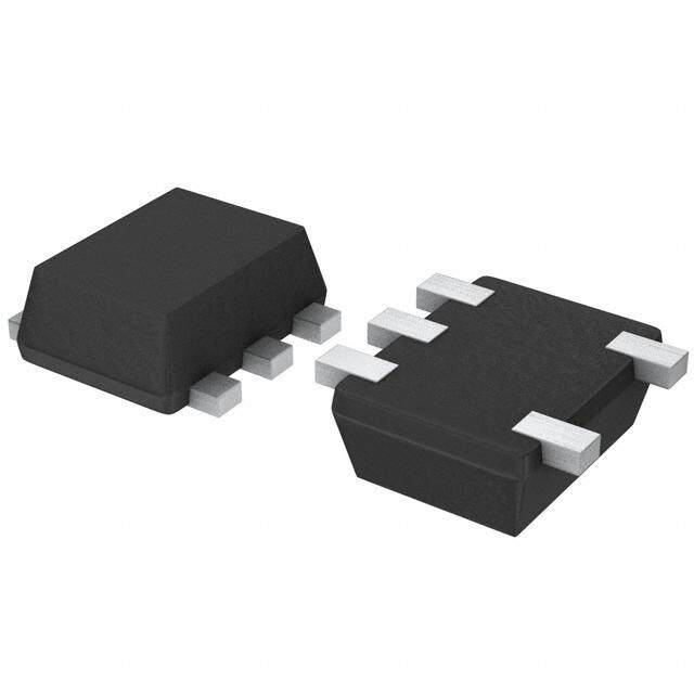
GENERIC PACKAGE VIEW DRV 6 WSON - 0.8 mm max height PLASTIC SMALL OUTLINE - NO LEAD Images above are just a representation of the package family, actual package may vary. Refer to the product data sheet for package details. 4206925/F
PACKAGE OUTLINE DRV0006A WSON - 0.8 mm max height SCALE 5.500 PLASTIC SMALL OUTLINE - NO LEAD B 2.1 A 1.9 PIN 1 INDEX AREA 2.1 1.9 0.8 C 0.7 SEATING PLANE 0.08 C (0.2) TYP 1 0.1 0.05 EXPOSED 0.00 THERMAL PAD 3 4 2X 7 1.3 1.6 0.1 6 1 4X 0.65 0.35 6X PIN 1 ID 0.3 0.25 6X (OPTIONAL) 0.2 0.1 C A B 0.05 C 4222173/B 04/2018 NOTES: 1. All linear dimensions are in millimeters. Any dimensions in parenthesis are for reference only. Dimensioning and tolerancing per ASME Y14.5M. 2. This drawing is subject to change without notice. 3. The package thermal pad must be soldered to the printed circuit board for thermal and mechanical performance. www.ti.com
EXAMPLE BOARD LAYOUT DRV0006A WSON - 0.8 mm max height PLASTIC SMALL OUTLINE - NO LEAD 6X (0.45) (1) 1 7 6X (0.3) 6 SYMM (1.6) (1.1) 4X (0.65) 4 3 (R0.05) TYP SYMM ( 0.2) VIA (1.95) TYP LAND PATTERN EXAMPLE SCALE:25X 0.07 MAX 0.07 MIN ALL AROUND ALL AROUND SOLDER MASK METAL METAL UNDER SOLDER MASK OPENING SOLDER MASK OPENING NON SOLDER MASK DEFINED SOLDER MASK (PREFERRED) DEFINED SOLDER MASK DETAILS 4222173/B 04/2018 NOTES: (continued) 4. This package is designed to be soldered to a thermal pad on the board. For more information, see Texas Instruments literature number SLUA271 (www.ti.com/lit/slua271). 5. Vias are optional depending on application, refer to device data sheet. If some or all are implemented, recommended via locations are shown. www.ti.com
EXAMPLE STENCIL DESIGN DRV0006A WSON - 0.8 mm max height PLASTIC SMALL OUTLINE - NO LEAD SYMM 6X (0.45) METAL 1 7 6X (0.3) 6 (0.45) SYMM 4X (0.65) (0.7) 4 3 (R0.05) TYP (1) (1.95) SOLDER PASTE EXAMPLE BASED ON 0.125 mm THICK STENCIL EXPOSED PAD #7 88% PRINTED SOLDER COVERAGE BY AREA UNDER PACKAGE SCALE:30X 4222173/B 04/2018 NOTES: (continued) 6. Laser cutting apertures with trapezoidal walls and rounded corners may offer better paste release. IPC-7525 may have alternate design recommendations. www.ti.com
PACKAGE OUTLINE DRV0006D WSON - 0.8 mm max height SCALE 5.500 PLASTIC SMALL OUTLINE - NO LEAD B 2.1 A 1.9 PIN 1 INDEX AREA 2.1 1.9 0.8 C 0.7 SEATING PLANE 0.08 C (0.2) TYP 1 0.1 0.05 EXPOSED 0.00 THERMAL PAD 3 4 2X 7 1.3 1.6 0.1 6 1 4X 0.65 0.35 6X PIN 1 ID 0.3 0.25 6X (OPTIONAL) 0.2 0.1 C A B 0.05 C 4225563/A 12/2019 NOTES: 1. All linear dimensions are in millimeters. Any dimensions in parenthesis are for reference only. Dimensioning and tolerancing per ASME Y14.5M. 2. This drawing is subject to change without notice. 3. The package thermal pad must be soldered to the printed circuit board for thermal and mechanical performance. www.ti.com
EXAMPLE BOARD LAYOUT DRV0006D WSON - 0.8 mm max height PLASTIC SMALL OUTLINE - NO LEAD 6X (0.45) (1) 1 7 6X (0.3) 6 SYMM (1.6) (1.1) 4X (0.65) 4 3 (R0.05) TYP SYMM ( 0.2) VIA (1.95) TYP LAND PATTERN EXAMPLE EXPOSED METAL SHOWN SCALE:25X 0.07 MAX 0.07 MIN ALL AROUND ALL AROUND EXPOSED EXPOSED METAL METAL SOLDER MASK METAL METAL UNDER SOLDER MASK OPENING SOLDER MASK OPENING NON SOLDER MASK DEFINED SOLDER MASK (PREFERRED) DEFINED SOLDER MASK DETAILS 4225563/A 12/2019 NOTES: (continued) 4. This package is designed to be soldered to a thermal pad on the board. For more information, see Texas Instruments literature number SLUA271 (www.ti.com/lit/slua271). 5. Vias are optional depending on application, refer to device data sheet. If some or all are implemented, recommended via locations are shown. www.ti.com
EXAMPLE STENCIL DESIGN DRV0006D WSON - 0.8 mm max height PLASTIC SMALL OUTLINE - NO LEAD SYMM 6X (0.45) METAL 1 7 6X (0.3) 6 (0.45) SYMM 4X (0.65) (0.7) 4 3 (R0.05) TYP (1) (1.95) SOLDER PASTE EXAMPLE BASED ON 0.125 mm THICK STENCIL EXPOSED PAD #7 88% PRINTED SOLDER COVERAGE BY AREA UNDER PACKAGE SCALE:30X 4225563/A 12/2019 NOTES: (continued) 6. Laser cutting apertures with trapezoidal walls and rounded corners may offer better paste release. IPC-7525 may have alternate design recommendations. www.ti.com
IMPORTANTNOTICEANDDISCLAIMER TI PROVIDES TECHNICAL AND RELIABILITY DATA (INCLUDING DATASHEETS), DESIGN RESOURCES (INCLUDING REFERENCE DESIGNS), APPLICATION OR OTHER DESIGN ADVICE, WEB TOOLS, SAFETY INFORMATION, AND OTHER RESOURCES “AS IS” AND WITH ALL FAULTS, AND DISCLAIMS ALL WARRANTIES, EXPRESS AND IMPLIED, INCLUDING WITHOUT LIMITATION ANY IMPLIED WARRANTIES OF MERCHANTABILITY, FITNESS FOR A PARTICULAR PURPOSE OR NON-INFRINGEMENT OF THIRD PARTY INTELLECTUAL PROPERTY RIGHTS. These resources are intended for skilled developers designing with TI products. You are solely responsible for (1) selecting the appropriate TI products for your application, (2) designing, validating and testing your application, and (3) ensuring your application meets applicable standards, and any other safety, security, or other requirements. These resources are subject to change without notice. TI grants you permission to use these resources only for development of an application that uses the TI products described in the resource. Other reproduction and display of these resources is prohibited. No license is granted to any other TI intellectual property right or to any third party intellectual property right. TI disclaims responsibility for, and you will fully indemnify TI and its representatives against, any claims, damages, costs, losses, and liabilities arising out of your use of these resources. TI’s products are provided subject to TI’s Terms of Sale (www.ti.com/legal/termsofsale.html) or other applicable terms available either on ti.com or provided in conjunction with such TI products. TI’s provision of these resources does not expand or otherwise alter TI’s applicable warranties or warranty disclaimers for TI products. Mailing Address: Texas Instruments, Post Office Box 655303, Dallas, Texas 75265 Copyright © 2020, Texas Instruments Incorporated