ICGOO在线商城 > 集成电路(IC) > PMIC - 监控器 > TPS3809K33QDBVRQ1
 Datasheet下载
- 型号: TPS3809K33QDBVRQ1
- 制造商: Texas Instruments
- 库位|库存: xxxx|xxxx
- 要求:
| 数量阶梯 | 香港交货 | 国内含税 |
| +xxxx | $xxxx | ¥xxxx |
查看当月历史价格
查看今年历史价格
TPS3809K33QDBVRQ1产品简介:
ICGOO电子元器件商城为您提供TPS3809K33QDBVRQ1由Texas Instruments设计生产,在icgoo商城现货销售,并且可以通过原厂、代理商等渠道进行代购。 TPS3809K33QDBVRQ1价格参考。Texas InstrumentsTPS3809K33QDBVRQ1封装/规格:PMIC - 监控器, 推挽式,图腾柱 监控器 1 通道 SOT-23-3。您可以下载TPS3809K33QDBVRQ1参考资料、Datasheet数据手册功能说明书,资料中有TPS3809K33QDBVRQ1 详细功能的应用电路图电压和使用方法及教程。
TPS3809K33QDBVRQ1 是德州仪器(Texas Instruments)推出的一款PMIC(电源管理集成电路)监控器,主要用于监测和保护电子设备中的电源电压。它具备高精度的电压检测功能,能够在电源电压低于或高于设定阈值时触发复位或报警信号,确保系统在异常情况下能够安全重启或采取保护措施。

 应用场景:

1. 工业控制系统:
   在工业自动化和控制系统中,TPS3809K33QDBVRQ1 可以用于监控关键电源轨,确保PLC(可编程逻辑控制器)、DCS(分布式控制系统)等设备的电源稳定性。当电源出现波动或故障时,该器件可以及时触发复位,防止系统误操作或数据丢失。

2. 通信设备:
   通信基站、路由器、交换机等设备对电源的稳定性要求极高。TPS3809K33QDBVRQ1 可以用于监控这些设备的电源电压,确保在电源异常时及时复位,避免通信中断或数据传输错误。

3. 消费电子产品:
   智能手机、平板电脑、笔记本电脑等消费电子产品中,TPS3809K33QDBVRQ1 可以用于监控电池电压或外部电源适配器的电压,确保设备在低电压或过压情况下自动关机或重启,保护内部电路不受损坏。

4. 汽车电子:
   在汽车电子系统中,如车载信息娱乐系统、ADAS(高级驾驶辅助系统)等,TPS3809K33QDBVRQ1 可以用于监控车辆电源电压,确保在电池电压波动或发电机故障时,系统能够安全重启或进入保护模式,保障行车安全。

5. 医疗设备:
   医疗设备如监护仪、超声设备等对电源的可靠性要求极高。TPS3809K33QDBVRQ1 可以用于监控这些设备的电源电压,确保在电源异常时及时复位,避免误诊或设备故障,保障患者安全。

6. 服务器和数据中心:
   在服务器和数据中心中,TPS3809K33QDBVRQ1 可以用于监控服务器的电源电压,确保在电源异常时及时复位,避免数据丢失或系统崩溃,保障数据中心的稳定运行。

总之,TPS3809K33QDBVRQ1 凭借其高精度的电压检测能力和可靠的复位功能,广泛应用于各种需要电源监控和保护的场景,确保系统的稳定性和安全性。
| 参数 | 数值 |
| 产品目录 | 集成电路 (IC)半导体 |
| 描述 | IC 2.93V SUPPLY MONITOR SOT-23-3监控电路 3-Pin Supply Voltage Supervisor |
| 产品分类 | |
| 品牌 | Texas Instruments |
| 产品手册 | |
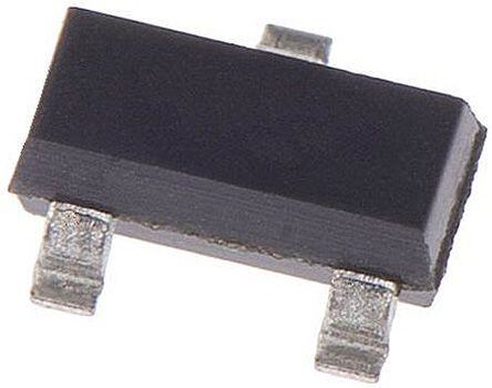
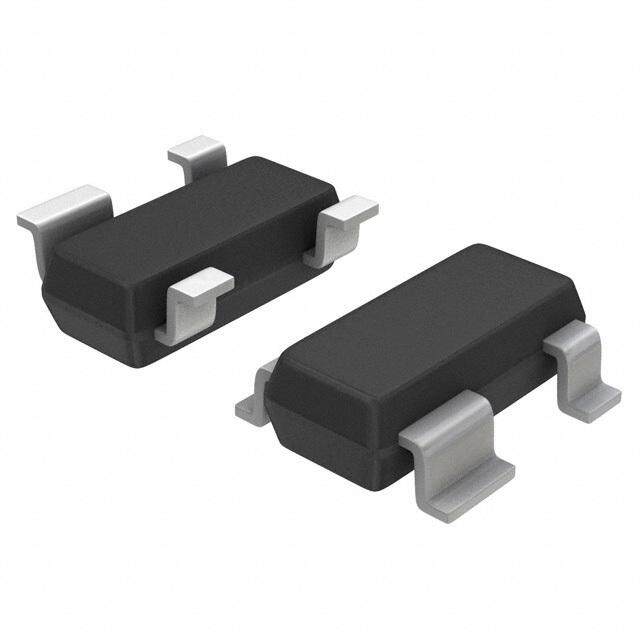
| 产品图片 |
|
| rohs | 符合RoHS无铅 / 符合限制有害物质指令(RoHS)规范要求 |
| 产品系列 | 电源管理 IC,监控电路,Texas Instruments TPS3809K33QDBVRQ1- |
| NumberofInputsMonitored | 1 Input |
| 数据手册 | |
| 产品型号 | TPS3809K33QDBVRQ1 |
| 产品目录页面 | |
| 产品种类 | 监控电路 |
| 人工复位 | No Manual Reset |
| 供应商器件封装 | SOT-23-3 |
| 其它名称 | 296-15644-6 |
| 包装 | Digi-Reel® |
| 单位重量 | 12.200 mg |
| 受监控电压数 | 1 |
| 商标 | Texas Instruments |
| 复位 | 低有效 |
| 复位超时 | 最小为 120 ms |
| 安装类型 | 表面贴装 |
| 安装风格 | SMD/SMT |
| 封装 | Reel |
| 封装/外壳 | TO-236-3,SC-59,SOT-23-3 |
| 封装/箱体 | SOT-23-3 |
| 工作温度 | -40°C ~ 125°C |
| 工作电源电流 | 9 uA |
| 工厂包装数量 | 3000 |
| 最大功率耗散 | 437 mW |
| 最大工作温度 | + 125 C |
| 最小工作温度 | - 40 C |
| 标准包装 | 1 |
| 欠电压阈值 | 2.87 V |
| 电压-阈值 | 2.93V |
| 电池备用开关 | No Backup |
| 电源电压-最大 | 6 V |
| 电源电压-最小 | 2 V |
| 监视器 | No Watchdog |
| 类型 | 简单复位/加电复位 |
| 系列 | TPS3809K33-Q1 |
| 被监测输入数 | 1 Input |
| 输出 | 推挽式,图腾柱 |
| 输出类型 | Active Low, Push-Pull |
| 过电压阈值 | 2.99 V |
| 重置延迟时间 | 200 ms |
| 阈值电压 | 2.93 V |


- 商务部:美国ITC正式对集成电路等产品启动337调查
- 曝三星4nm工艺存在良率问题 高通将骁龙8 Gen1或转产台积电
- 太阳诱电将投资9.5亿元在常州建新厂生产MLCC 预计2023年完工
- 英特尔发布欧洲新工厂建设计划 深化IDM 2.0 战略
- 台积电先进制程称霸业界 有大客户加持明年业绩稳了
- 达到5530亿美元!SIA预计今年全球半导体销售额将创下新高
- 英特尔拟将自动驾驶子公司Mobileye上市 估值或超500亿美元
- 三星加码芯片和SET,合并消费电子和移动部门,撤换高东真等 CEO
- 三星电子宣布重大人事变动 还合并消费电子和移动部门
- 海关总署:前11个月进口集成电路产品价值2.52万亿元 增长14.8%


PDF Datasheet 数据手册内容提取
Product Sample & Technical Tools & Support & Folder Buy Documents Software Community TPS3809J25-Q1,TPS3809L30-Q1,TPS3809K33-Q1,TPS3809I50-Q1 SGLS142B–JUNE2008–REVISEDMARCH2016 TPS3809xxx-Q1 3-Pin Supply Voltage Supervisors 1 Features 3 Description • QualifiedforAutomotiveApplications The TPS3809 family of supervisory circuits provides 1 circuit initialization and timing supervision, primarily • AEC-Q100QualifiedWiththeFollowingResults: forDSPsandprocessor-basedsystems. – DeviceTemperatureGrade1: –40°Cto During power-on, RESET is asserted when the +125°CAmbientOperatingTemperature supply voltage VDD becomes higher than 1.1 V. Range Thereafter, the supervisory circuit monitors V and DD – DeviceHBMESDClassificationLevel2 keeps RESET active as long as V remains below DD – DeviceCDMESDClassificationLevelC5 the threshold voltage VIT. An internal timer delays the return of the output to the inactive state (high) to • 3-PinSOT-23Package ensure proper system reset. The delay time, t = d(typ) • SupplyCurrentof9 μA(Typical) 200 ms, starts after V has risen above the DD • Precision-SupplyVoltageMonitor2.5V,3V,3.3 threshold voltage V . When the supply voltage drops IT V,5V below the threshold voltage V , the output becomes IT active (low) again. No external components are • Power-OnResetGeneratorWithFixedDelay required. All the devices of this family have a fixed Timeof200ms sense-threshold voltage V set by an internal voltage IT • Pin-For-PinCompatibleWithMAX809 divider. 2 Applications The product spectrum is designed for supply voltages of 2.5 V, 3 V, 3.3 V, and 5 V. The circuits are • AutomotiveApplicationsWithDSPs, available in a 3-pin SOT-23. The TPS3809xxx-Q1 Microcontrollers,orMicroprocessors devices are characterized for operation over a • AutomotiveCameraSystems temperature range of −40°C to 125°C, and are qualified in accordance with AEC-Q100 stress test • AutomotiveRadar qualification for integrated circuits. For more • USBHubsandCharging information about TI's voltage supervisor portfolio, please visit the Supervisor and Reset IC Overview webpage. DeviceInformation(1) PARTNUMBER PACKAGE BODYSIZE(NOM) TPS3809xxx-Q1 SOT-23(3) 2.90mm×1.60mm (1) For all available packages, see the orderable addendum at theendofthedatasheet. TypicalApplication TPS76333 3.3V 5V IN OUT GND VDD VDD TMS320LC54x TPS3809K33-Q1 RESET RESET GND GND 1 An IMPORTANT NOTICE at the end of this data sheet addresses availability, warranty, changes, use in safety-critical applications, intellectualpropertymattersandotherimportantdisclaimers.PRODUCTIONDATA.
TPS3809J25-Q1,TPS3809L30-Q1,TPS3809K33-Q1,TPS3809I50-Q1 SGLS142B–JUNE2008–REVISEDMARCH2016 www.ti.com Table of Contents 1 Features.................................................................. 1 8.2 FunctionalBlockDiagram.........................................8 2 Applications........................................................... 1 8.3 FeatureDescription...................................................8 3 Description............................................................. 1 8.4 DeviceFunctionalModes..........................................8 4 RevisionHistory..................................................... 2 9 ApplicationandImplementation.......................... 9 9.1 ApplicationInformation..............................................9 5 VoltageOptions..................................................... 3 9.2 TypicalApplication ...................................................9 6 PinConfigurationandFunctions......................... 3 10 PowerSupplyRecommendations..................... 11 7 Specifications......................................................... 4 11 Layout................................................................... 11 7.1 AbsoluteMaximumRatings......................................4 11.1 LayoutGuidelines.................................................11 7.2 ESDRatings..............................................................4 11.2 LayoutExample....................................................11 7.3 RecommendedOperatingConditions.......................4 12 DeviceandDocumentationSupport................. 12 7.4 ThermalInformation..................................................4 7.5 ElectricalCharacteristics...........................................5 12.1 RelatedLinks........................................................12 7.6 TimingRequirements................................................5 12.2 CommunityResources..........................................12 7.7 SwitchingCharacteristics..........................................5 12.3 Trademarks...........................................................12 7.8 TypicalCharacteristics..............................................7 12.4 ElectrostaticDischargeCaution............................12 12.5 Glossary................................................................12 8 DetailedDescription.............................................. 8 13 Mechanical,Packaging,andOrderable 8.1 Overview...................................................................8 Information........................................................... 12 4 Revision History ChangesfromRevisionA(December2002)toRevisionB Page • AddedAEC-Q100Qualifiedinformationinbullets ................................................................................................................ 1 • ChangedApplicationslistitems............................................................................................................................................. 1 • AddedESDRatingstable,FeatureDescriptionsection,DeviceFunctionalModes,ApplicationandImplementation section,PowerSupplyRecommendationssection,Layoutsection,DeviceandDocumentationSupportsection,and Mechanical,Packaging,andOrderableInformationsection ................................................................................................. 1 • Changeddevicepartnumbersbyadding-Q1tothemthroughoutdocument ...................................................................... 5 2 SubmitDocumentationFeedback Copyright©2008–2016,TexasInstrumentsIncorporated ProductFolderLinks:TPS3809J25-Q1 TPS3809L30-Q1 TPS3809K33-Q1 TPS3809I50-Q1
TPS3809J25-Q1,TPS3809L30-Q1,TPS3809K33-Q1,TPS3809I50-Q1 www.ti.com SGLS142B–JUNE2008–REVISEDMARCH2016 5 Voltage Options T DEVICENAME THRESHOLDVOLTAGE MARKING A TPS3809J25QDBVRQ1 2.25V PCZQ TPS3809L30QDBVRQ1 2.64V PDAQ −40°Cto125°C TPS3809K33QDBVRQ1 2.93V PDBQ TPS3809I50QDBVRQ1 4.55V PDCQ 6 Pin Configuration and Functions DBVPackage 3-PinSOT-23 TopView GND 1 3 V DD RESET_ 2 PinFunctions PIN I/O DESCRIPTION NAME NO. GND 1 — Ground RESET 2 O Resetoutput V 3 I Supplyvoltageandsupervisinginput DD Copyright©2008–2016,TexasInstrumentsIncorporated SubmitDocumentationFeedback 3 ProductFolderLinks:TPS3809J25-Q1 TPS3809L30-Q1 TPS3809K33-Q1 TPS3809I50-Q1
TPS3809J25-Q1,TPS3809L30-Q1,TPS3809K33-Q1,TPS3809I50-Q1 SGLS142B–JUNE2008–REVISEDMARCH2016 www.ti.com 7 Specifications 7.1 Absolute Maximum Ratings overoperatingfree-airtemperaturerange(unlessotherwisenoted)(1) MIN MAX UNIT Supplyvoltage,V (2) 7 V DD Allotherpins(2) –0.3 7 V Maximumlowoutputcurrent,I 5 mA OL Maximumhighoutputcurrent,I –5 mA OH Inputclampcurrent,I (V<0orV>V ) –20 20 mA IK I I DD Outputclampcurrent,I (V <0orV >V ) –20 20 mA OK O O DD Continuoustotalpowerdissipation Operatingfree-airtemperaturerange,T –40 125 °C A Storagetemperature,T –65 150 °C stg (1) StressesbeyondthoselistedunderAbsoluteMaximumRatingsmaycausepermanentdamagetothedevice.Thesearestressratings only,whichdonotimplyfunctionaloperationofthedeviceattheseoranyotherconditionsbeyondthoseindicatedunderRecommended OperatingConditions.Exposuretoabsolute-maximum-ratedconditionsforextendedperiodsmayaffectdevicereliability. (2) AllvoltagevaluesarewithrespecttoGND.Forreliableoperationthedeviceshouldnotbeoperatedat7Vformorethant=1000h continuously. 7.2 ESD Ratings VALUE UNIT Human-bodymodel(HBM),perAECQ100-002(1) ±2000 V Electrostaticdischarge V (ESD) Charged-devicemodel(CDM),perAECQ100-011 ±750 (1) AECQ100-002indicatesthatHBMstressingshallbeinaccordancewiththeANSI/ESDA/JEDECJS-001specification. 7.3 Recommended Operating Conditions overoperatingfree-airtemperaturerange(unlessotherwisenoted) MIN NOM MAX UNIT V Supplyvoltage 2 6 V DD T Operatingfree-airtemperature –40 125 °C A 7.4 Thermal Information TPS3809xxx-Q1 THERMALMETRIC(1) DBV(SOT-23) UNIT 3PINS R Junction-to-ambientthermalresistance 232.5 °C/W θJA R Junction-to-case(top)thermalresistance 187.6 °C/W θJC(top) R Junction-to-boardthermalresistance 104.1 °C/W θJB ψ Junction-to-topcharacterizationparameter 40.5 °C/W JT ψ Junction-to-boardcharacterizationparameter 104.4 °C/W JB R Junction-to-case(bottom)thermalresistance N/A °C/W θJC(bot) (1) Formoreinformationabouttraditionalandnewthermalmetrics,seetheSemiconductorandICPackageThermalMetricsapplication report,SPRA953. 4 SubmitDocumentationFeedback Copyright©2008–2016,TexasInstrumentsIncorporated ProductFolderLinks:TPS3809J25-Q1 TPS3809L30-Q1 TPS3809K33-Q1 TPS3809I50-Q1
TPS3809J25-Q1,TPS3809L30-Q1,TPS3809K33-Q1,TPS3809I50-Q1 www.ti.com SGLS142B–JUNE2008–REVISEDMARCH2016 7.5 Electrical Characteristics overoperatingfree-airtemperaturerange(unlessotherwisenoted) PARAMETER TESTCONDITIONS MIN TYP MAX UNIT VDD=2.5Vto6V,IOH=−500μA VDD–0.2 VDD=3.3V,IOH=−2μA VDD–0.4 VOH High-leveloutputvoltage V TA=−40°Cto+25°C VDD–0.4 VDD=6V,IOH=−4mA TA=125°C VDD–0.5 VDD=2Vto6V,IOL=500μA 0.2 VOL Low-leveloutputvoltage VDD=3.3V,IOL=2mA 0.4 V VDD=6V,IOL=4mA 0.4 Power-upresetvoltage(1) VDD≥1.1V,IOL=50μA 0.2 V TPS3809J25-Q1 2.20 2.25 2.30 TPS3809L30-Q1 TA=−40°Cto+125°C 2.58 2.64 2.7 Negative-goinginputthreshold VIT− voltage(2) TPS3809K33-Q1 2.87 2.93 2.99 V TA=−40°Cto+85°C 4.45 4.55 4.65 TPS3809I50-Q1 TA=−40°Cto+125°C 4.4 4.55 4.65 TPS3809J25-Q1 30 TPS3809L30-Q1 35 Vhys Hysteresis mV TPS3809K33-Q1 40 TPS3809I50-Q1 60 VDD=2V,Outputunconnected 9 15 IDD Supplycurrent μA VDD=6V,Outputunconnected 20 30 Ci Inputcapacitance VI=0VtoVDD 5 pF (1) ThelowestsupplyvoltageatwhichRESETbecomesactive.t,V ≥15µs/V. r DD (2) Toensurebeststabilityofthethresholdvoltage,abypasscapacitor(0.1µF,ceramic)shouldbeplacednearthesupplyterminals. 7.6 Timing Requirements R =1MΩ,C =50pF,T =25°C L L A MIN NOM MAX UNIT t PulsewidthatV V =V +0.2V,VDD=V −0.2V 3 μs w DD DD IT− IT− 7.7 Switching Characteristics R =1MΩ,C =50pF,T =25°C L L A PARAMETER TESTCONDITIONS MIN TYP MAX UNIT V ≥V +0.2V,See t Delaytime DD IT− 120 200 280 ms d timingdiagram,Figure1 Propagation(delay)time, V =V −0.2V,V =V t V toRESETdelay IL IT− IH IT− 1 μs PHL high-to-low-leveloutput DD +0.2V Copyright©2008–2016,TexasInstrumentsIncorporated SubmitDocumentationFeedback 5 ProductFolderLinks:TPS3809J25-Q1 TPS3809L30-Q1 TPS3809K33-Q1 TPS3809I50-Q1
TPS3809J25-Q1,TPS3809L30-Q1,TPS3809K33-Q1,TPS3809I50-Q1 SGLS142B–JUNE2008–REVISEDMARCH2016 www.ti.com VDD V(NOM) VIT 1.1V t RESET aaaaa 1aaaa aaaaa aaaa aaaaa aaaa aaaaa aaaa aaaa aaaaa 0 t td td ForVDD<1.1VUndefined BehaviorofRESETOutput Figure1. TimingDiagram 6 SubmitDocumentationFeedback Copyright©2008–2016,TexasInstrumentsIncorporated ProductFolderLinks:TPS3809J25-Q1 TPS3809L30-Q1 TPS3809K33-Q1 TPS3809I50-Q1
TPS3809J25-Q1,TPS3809L30-Q1,TPS3809K33-Q1,TPS3809I50-Q1 www.ti.com SGLS142B–JUNE2008–REVISEDMARCH2016 7.8 Typical Characteristics 2.75 50 VDD=2.5V TA=25oC 2.50 40 V – 2.25 30 e OutVoltputag 112...570050 TA=25oC Current–Am 12000 TPS3809J25 Low-Level 011...702505 TA=85oC TA=0oC –SupplyDD ––2100 –OL 0.50 TA=–40oC I –30 V 0.25 –40 0 –50 0 2.5 5.0 7.5 10.0 12.5 –2 0 2 4 6 IOL–Low-LevelOutputCurrent–mA VDD–SupplyVoltage–V Figure2.Low-LevelOutputVoltagevs Figure3.SupplyCurrentvsSupplyVoltage Low-LevelOutputCurrent 6.5 3.00 VDD=6V VDD=2.5V 6.0 2.75 –V 5.5 –V 2.50 age 5.0 age 2.25 Volt 4.5 TA=–40oC Volt 2.00 ut 4.0 ut TA=–40oC p p 1.75 evelOut 33..05 TA=0oC evelOut 11..2550 TA=0oC High-L 22..05 TA=85oC High-L 1.00 TA=85oC –H 1.5 –H 0.75 VO 1.0 TA=25oC VO 0.50 TA=25oC 0.5 0.25 0 0 0 –10 –20 –30 –40 –50 0 –2 –4 –6 –8 –10 IOH–High-LevelOutputCurrent–mA IOH–High-LevelOutputCurrent–mA V =6V V =2.5V DD DD Figure4.High-LevelOutputVoltagevs Figure5.High-LevelOutputVoltagevs High-LevelOutputCurrent High-LevelOutputCurrent C) 1.001 3.5 oV(25IT 1.000 VDD=2.3V –smD 3.0 V(T),ITA 0.999 VonatD 2.5 Voltage 0.998 eDurati 2.0 hold Puls 1.5 hres 0.997 mum 1.0 edT Mini maliz 0.996 –w 0.5 or t N 0.995 0 –40 –20 0 20 40 60 85 0 0.2 0.4 0.6 0.8 1.0 TA–Free-AirTemperature–oC VDD–ThresholdOverdriveVoltage–V V =2.3V DD Figure6.NormalizedInputThresholdVoltagevs Figure7.MinimumPulseDurationatV vs DD Free-AirTemperatureatV V ThresholdOverdriveVoltage DD DD Copyright©2008–2016,TexasInstrumentsIncorporated SubmitDocumentationFeedback 7 ProductFolderLinks:TPS3809J25-Q1 TPS3809L30-Q1 TPS3809K33-Q1 TPS3809I50-Q1
TPS3809J25-Q1,TPS3809L30-Q1,TPS3809K33-Q1,TPS3809I50-Q1 SGLS142B–JUNE2008–REVISEDMARCH2016 www.ti.com 8 Detailed Description 8.1 Overview The TPS3809xxx-Q1 device is a low-current supervisory circuit for monitoring system voltages above 2 V. The device asserts an active-low RESET signal when VDD drops below a preset threshold. The RESET output remains low until VDD returns above its threshold. The device design is also to be relatively immune to short negativetransientsontheVDDpin. 8.2 Functional Block Diagram TPS3809xxx-Q1 Reset RESET R1 Logic VDD _ + Timer + R2 GND Oscillator Reference Voltage of1.137V 8.3 Feature Description 8.3.1 V Monitoring DD The V pin provides a terminal at which a system voltage can be monitored. If the voltage on this pin drops DD below V , RESET is asserted low. The comparator has a built-in hysteresis to ensure smooth RESET assertions IT anddeassertions.RefertoVoltageOptionstodeterminetheV voltagethresholdforeachdevice. DD 8.4 Device Functional Modes TPS3809xxx-Q1 monitors one supply using the V pin. When V is above the V threshold for the device, DD DD IT RESETwillbehigh.WhenV isbelowtheV thresholdforthedevice,RESETwillbelow. DD IT 8 SubmitDocumentationFeedback Copyright©2008–2016,TexasInstrumentsIncorporated ProductFolderLinks:TPS3809J25-Q1 TPS3809L30-Q1 TPS3809K33-Q1 TPS3809I50-Q1
TPS3809J25-Q1,TPS3809L30-Q1,TPS3809K33-Q1,TPS3809I50-Q1 www.ti.com SGLS142B–JUNE2008–REVISEDMARCH2016 9 Application and Implementation NOTE Information in the following applications sections is not part of the TI component specification, and TI does not warrant its accuracy or completeness. TI’s customers are responsible for determining suitability of components for their purposes. Customers should validateandtesttheirdesignimplementationtoconfirmsystemfunctionality. 9.1 Application Information The TPS3809xxx-Q1 voltage supervisor device design asserts an active-low RESET signal when V drops DD below a voltage threshold V . The RESET signal remains low until the voltage returns above its threshold. The IT typical application is with a processor or microcontroller, which needs to be reset when the supply rail drops belowaspecifiedtolerance. 9.2 Typical Application TPS76333 3.3V 5V IN OUT GND VDD VDD TMS320LC54x TPS3809K33-Q1 RESET RESET GND GND Figure8. TypicalApplicationSchematic 9.2.1 DesignRequirements Each device has a fixed=voltage monitoring threshold, and the device should be chosen based on the voltage being monitored. Refer to Voltage Options to determine the VDD voltage threshold for each device. In this example,a3.3Vsupplyrailtoamicrocontrollerwillbemonitored. 9.2.2 DetailedDesignProcedure Because a 3.3-V supply rail needs to be monitored, TPS3809K33-Q1 should be used. This device has a 2.93-V thresholdforreset.Connectthe3.3-VsupplytotheV pinandtheresetoutputofthesupervisortotheresetpin DD ofthemicrocontroller. Copyright©2008–2016,TexasInstrumentsIncorporated SubmitDocumentationFeedback 9 ProductFolderLinks:TPS3809J25-Q1 TPS3809L30-Q1 TPS3809K33-Q1 TPS3809I50-Q1
TPS3809J25-Q1,TPS3809L30-Q1,TPS3809K33-Q1,TPS3809I50-Q1 SGLS142B–JUNE2008–REVISEDMARCH2016 www.ti.com Typical Application (continued) 9.2.3 ApplicationCurves 50 1.001 TA=25oC o5C) VDD=2.3V 40 2 ( 30 VIT 1.000 Am 20 (T),A nt– VIT 0.999 Curre 100 TPS3809J25 oltage 0.998 y V pl d –SupD ––2100 hreshol 0.997 D T I d –30 e aliz 0.996 –40 m or N –50 0.995 –2 0 2 4 6 –40 –20 0 20 40 60 85 VDD–SupplyVoltage–V TA–Free-AirTemperature–oC V =2.3V DD Figure9.SupplyCurrentvsSupplyVoltage Figure10.NormalizedInputThresholdVoltagevsFree-Air TemperatureatV DD 10 SubmitDocumentationFeedback Copyright©2008–2016,TexasInstrumentsIncorporated ProductFolderLinks:TPS3809J25-Q1 TPS3809L30-Q1 TPS3809K33-Q1 TPS3809I50-Q1
TPS3809J25-Q1,TPS3809L30-Q1,TPS3809K33-Q1,TPS3809I50-Q1 www.ti.com SGLS142B–JUNE2008–REVISEDMARCH2016 10 Power Supply Recommendations TheTPS3809xxx-Q1devicedesignoperatesfromaninputsupplyfrom2Vto6V.TIrecommendsplacinga0.1- µFcapacitorneartheV pin. DD 11 Layout 11.1 Layout Guidelines TIrecommendsplacingthe0.1-µFdecouplingcapacitorclosetotheV pin.TheV andGNDtracesshouldbe DD DD abletocarry30µAwithoutasignificantdropinvoltage. 11.2 Layout Example GND CVDD TPS3809xxx-Q1 VDD RESET Denotes GND Via Figure11. LayoutExample Copyright©2008–2016,TexasInstrumentsIncorporated SubmitDocumentationFeedback 11 ProductFolderLinks:TPS3809J25-Q1 TPS3809L30-Q1 TPS3809K33-Q1 TPS3809I50-Q1
TPS3809J25-Q1,TPS3809L30-Q1,TPS3809K33-Q1,TPS3809I50-Q1 SGLS142B–JUNE2008–REVISEDMARCH2016 www.ti.com 12 Device and Documentation Support 12.1 Related Links The table below lists quick access links. Categories include technical documents, support and community resources,toolsandsoftware,andquickaccesstosampleorbuy. Table1.RelatedLinks TECHNICAL TOOLS& SUPPORT& PARTS PRODUCTFOLDER SAMPLE&BUY DOCUMENTS SOFTWARE COMMUNITY TPS3809J25-Q1 Clickhere Clickhere Clickhere Clickhere Clickhere TPS3809L30-Q1 Clickhere Clickhere Clickhere Clickhere Clickhere TPS3809K33-Q1 Clickhere Clickhere Clickhere Clickhere Clickhere TPS3809I50-Q1 Clickhere Clickhere Clickhere Clickhere Clickhere 12.2 Community Resources The following links connect to TI community resources. Linked contents are provided "AS IS" by the respective contributors. They do not constitute TI specifications and do not necessarily reflect TI's views; see TI's Terms of Use. TIE2E™OnlineCommunity TI'sEngineer-to-Engineer(E2E)Community.Createdtofostercollaboration amongengineers.Ate2e.ti.com,youcanaskquestions,shareknowledge,exploreideasandhelp solveproblemswithfellowengineers. DesignSupport TI'sDesignSupport QuicklyfindhelpfulE2Eforumsalongwithdesignsupporttoolsand contactinformationfortechnicalsupport. 12.3 Trademarks E2EisatrademarkofTexasInstruments. Allothertrademarksarethepropertyoftheirrespectiveowners. 12.4 Electrostatic Discharge Caution Thesedeviceshavelimitedbuilt-inESDprotection.Theleadsshouldbeshortedtogetherorthedeviceplacedinconductivefoam duringstorageorhandlingtopreventelectrostaticdamagetotheMOSgates. 12.5 Glossary SLYZ022—TIGlossary. Thisglossarylistsandexplainsterms,acronyms,anddefinitions. 13 Mechanical, Packaging, and Orderable Information The following pages include mechanical, packaging, and orderable information. This information is the most current data available for the designated devices. This data is subject to change without notice and revision of thisdocument.Forbrowser-basedversionsofthisdatasheet,refertotheleft-handnavigation. 12 SubmitDocumentationFeedback Copyright©2008–2016,TexasInstrumentsIncorporated ProductFolderLinks:TPS3809J25-Q1 TPS3809L30-Q1 TPS3809K33-Q1 TPS3809I50-Q1
PACKAGE OPTION ADDENDUM www.ti.com 22-Dec-2016 PACKAGING INFORMATION Orderable Device Status Package Type Package Pins Package Eco Plan Lead/Ball Finish MSL Peak Temp Op Temp (°C) Device Marking Samples (1) Drawing Qty (2) (6) (3) (4/5) 2T09I50QDBVRG4Q ACTIVE SOT-23 DBV 3 3000 Green (RoHS CU NIPDAU Level-1-260C-UNLIM -40 to 125 PDCQ & no Sb/Br) 2T09J25QDBVRG4Q LIFEBUY SOT-23 DBV 3 3000 Green (RoHS CU NIPDAU Level-1-260C-UNLIM -40 to 125 PCZQ & no Sb/Br) 2U3809K33QDBVRG4Q1 LIFEBUY SOT-23 DBV 3 3000 Green (RoHS CU NIPDAU Level-1-260C-UNLIM -40 to 125 PDBQ & no Sb/Br) 2U3809L30QDBVRG4Q1 LIFEBUY SOT-23 DBV 3 3000 Green (RoHS CU NIPDAU Level-1-260C-UNLIM -40 to 125 PDAQ & no Sb/Br) TPS3809I50QDBVRQ1 ACTIVE SOT-23 DBV 3 3000 Green (RoHS CU NIPDAU Level-1-260C-UNLIM -40 to 125 PDCQ & no Sb/Br) TPS3809J25QDBVRQ1 LIFEBUY SOT-23 DBV 3 3000 Green (RoHS CU NIPDAU Level-1-260C-UNLIM -40 to 125 PCZQ & no Sb/Br) TPS3809K33QDBVRQ1 ACTIVE SOT-23 DBV 3 3000 Green (RoHS CU NIPDAU Level-1-260C-UNLIM -40 to 125 PDBQ & no Sb/Br) TPS3809L30QDBVRQ1 ACTIVE SOT-23 DBV 3 3000 Green (RoHS CU NIPDAU Level-1-260C-UNLIM -40 to 125 PDAQ & no Sb/Br) (1) The marketing status values are defined as follows: ACTIVE: Product device recommended for new designs. LIFEBUY: TI has announced that the device will be discontinued, and a lifetime-buy period is in effect. NRND: Not recommended for new designs. Device is in production to support existing customers, but TI does not recommend using this part in a new design. PREVIEW: Device has been announced but is not in production. Samples may or may not be available. OBSOLETE: TI has discontinued the production of the device. (2) Eco Plan - The planned eco-friendly classification: Pb-Free (RoHS), Pb-Free (RoHS Exempt), or Green (RoHS & no Sb/Br) - please check http://www.ti.com/productcontent for the latest availability information and additional product content details. TBD: The Pb-Free/Green conversion plan has not been defined. Pb-Free (RoHS): TI's terms "Lead-Free" or "Pb-Free" mean semiconductor products that are compatible with the current RoHS requirements for all 6 substances, including the requirement that lead not exceed 0.1% by weight in homogeneous materials. Where designed to be soldered at high temperatures, TI Pb-Free products are suitable for use in specified lead-free processes. Pb-Free (RoHS Exempt): This component has a RoHS exemption for either 1) lead-based flip-chip solder bumps used between the die and package, or 2) lead-based die adhesive used between the die and leadframe. The component is otherwise considered Pb-Free (RoHS compatible) as defined above. Green (RoHS & no Sb/Br): TI defines "Green" to mean Pb-Free (RoHS compatible), and free of Bromine (Br) and Antimony (Sb) based flame retardants (Br or Sb do not exceed 0.1% by weight in homogeneous material) (3) MSL, Peak Temp. - The Moisture Sensitivity Level rating according to the JEDEC industry standard classifications, and peak solder temperature. Addendum-Page 1
PACKAGE OPTION ADDENDUM www.ti.com 22-Dec-2016 (4) There may be additional marking, which relates to the logo, the lot trace code information, or the environmental category on the device. (5) Multiple Device Markings will be inside parentheses. Only one Device Marking contained in parentheses and separated by a "~" will appear on a device. If a line is indented then it is a continuation of the previous line and the two combined represent the entire Device Marking for that device. (6) Lead/Ball Finish - Orderable Devices may have multiple material finish options. Finish options are separated by a vertical ruled line. Lead/Ball Finish values may wrap to two lines if the finish value exceeds the maximum column width. Important Information and Disclaimer:The information provided on this page represents TI's knowledge and belief as of the date that it is provided. TI bases its knowledge and belief on information provided by third parties, and makes no representation or warranty as to the accuracy of such information. Efforts are underway to better integrate information from third parties. TI has taken and continues to take reasonable steps to provide representative and accurate information but may not have conducted destructive testing or chemical analysis on incoming materials and chemicals. TI and TI suppliers consider certain information to be proprietary, and thus CAS numbers and other limited information may not be available for release. In no event shall TI's liability arising out of such information exceed the total purchase price of the TI part(s) at issue in this document sold by TI to Customer on an annual basis. OTHER QUALIFIED VERSIONS OF TPS3809-Q1, TPS3809I50-Q1, TPS3809J25-Q1, TPS3809K33-Q1, TPS3809L30-Q1 : •Catalog: TPS3809I50, TPS3809J25, TPS3809K33, TPS3809L30 •Enhanced Product: TPS3809-EP, TPS3809I50-EP, TPS3809K33-EP, TPS3809L30-EP NOTE: Qualified Version Definitions: •Catalog - TI's standard catalog product •Enhanced Product - Supports Defense, Aerospace and Medical Applications Addendum-Page 2
PACKAGE MATERIALS INFORMATION www.ti.com 22-Dec-2016 TAPE AND REEL INFORMATION *Alldimensionsarenominal Device Package Package Pins SPQ Reel Reel A0 B0 K0 P1 W Pin1 Type Drawing Diameter Width (mm) (mm) (mm) (mm) (mm) Quadrant (mm) W1(mm) 2T09I50QDBVRG4Q SOT-23 DBV 3 3000 180.0 9.0 3.3 3.2 1.47 4.0 8.0 Q3 2T09J25QDBVRG4Q SOT-23 DBV 3 3000 180.0 9.0 3.3 3.2 1.47 4.0 8.0 Q3 2U3809K33QDBVRG4Q1 SOT-23 DBV 3 3000 180.0 9.0 3.3 3.2 1.47 4.0 8.0 Q3 2U3809L30QDBVRG4Q1 SOT-23 DBV 3 3000 180.0 9.0 3.3 3.2 1.47 4.0 8.0 Q3 TPS3809I50QDBVRQ1 SOT-23 DBV 3 3000 180.0 9.0 3.3 3.2 1.47 4.0 8.0 Q3 TPS3809J25QDBVRQ1 SOT-23 DBV 3 3000 180.0 9.0 3.3 3.2 1.47 4.0 8.0 Q3 TPS3809K33QDBVRQ1 SOT-23 DBV 3 3000 180.0 9.0 3.3 3.2 1.47 4.0 8.0 Q3 TPS3809L30QDBVRQ1 SOT-23 DBV 3 3000 180.0 9.0 3.3 3.2 1.47 4.0 8.0 Q3 PackMaterials-Page1
PACKAGE MATERIALS INFORMATION www.ti.com 22-Dec-2016 *Alldimensionsarenominal Device PackageType PackageDrawing Pins SPQ Length(mm) Width(mm) Height(mm) 2T09I50QDBVRG4Q SOT-23 DBV 3 3000 182.0 182.0 20.0 2T09J25QDBVRG4Q SOT-23 DBV 3 3000 182.0 182.0 20.0 2U3809K33QDBVRG4Q1 SOT-23 DBV 3 3000 182.0 182.0 20.0 2U3809L30QDBVRG4Q1 SOT-23 DBV 3 3000 182.0 182.0 20.0 TPS3809I50QDBVRQ1 SOT-23 DBV 3 3000 182.0 182.0 20.0 TPS3809J25QDBVRQ1 SOT-23 DBV 3 3000 182.0 182.0 20.0 TPS3809K33QDBVRQ1 SOT-23 DBV 3 3000 182.0 182.0 20.0 TPS3809L30QDBVRQ1 SOT-23 DBV 3 3000 182.0 182.0 20.0 PackMaterials-Page2
None
None
IMPORTANTNOTICE TexasInstrumentsIncorporatedanditssubsidiaries(TI)reservetherighttomakecorrections,enhancements,improvementsandother changestoitssemiconductorproductsandservicesperJESD46,latestissue,andtodiscontinueanyproductorserviceperJESD48,latest issue.Buyersshouldobtainthelatestrelevantinformationbeforeplacingordersandshouldverifythatsuchinformationiscurrentand complete.Allsemiconductorproducts(alsoreferredtohereinas“components”)aresoldsubjecttoTI’stermsandconditionsofsale suppliedatthetimeoforderacknowledgment. TIwarrantsperformanceofitscomponentstothespecificationsapplicableatthetimeofsale,inaccordancewiththewarrantyinTI’sterms andconditionsofsaleofsemiconductorproducts.TestingandotherqualitycontroltechniquesareusedtotheextentTIdeemsnecessary tosupportthiswarranty.Exceptwheremandatedbyapplicablelaw,testingofallparametersofeachcomponentisnotnecessarily performed. TIassumesnoliabilityforapplicationsassistanceorthedesignofBuyers’products.Buyersareresponsiblefortheirproductsand applicationsusingTIcomponents.TominimizetherisksassociatedwithBuyers’productsandapplications,Buyersshouldprovide adequatedesignandoperatingsafeguards. TIdoesnotwarrantorrepresentthatanylicense,eitherexpressorimplied,isgrantedunderanypatentright,copyright,maskworkright,or otherintellectualpropertyrightrelatingtoanycombination,machine,orprocessinwhichTIcomponentsorservicesareused.Information publishedbyTIregardingthird-partyproductsorservicesdoesnotconstitutealicensetousesuchproductsorservicesorawarrantyor endorsementthereof.Useofsuchinformationmayrequirealicensefromathirdpartyunderthepatentsorotherintellectualpropertyofthe thirdparty,oralicensefromTIunderthepatentsorotherintellectualpropertyofTI. ReproductionofsignificantportionsofTIinformationinTIdatabooksordatasheetsispermissibleonlyifreproductioniswithoutalteration andisaccompaniedbyallassociatedwarranties,conditions,limitations,andnotices.TIisnotresponsibleorliableforsuchaltered documentation.Informationofthirdpartiesmaybesubjecttoadditionalrestrictions. ResaleofTIcomponentsorserviceswithstatementsdifferentfromorbeyondtheparametersstatedbyTIforthatcomponentorservice voidsallexpressandanyimpliedwarrantiesfortheassociatedTIcomponentorserviceandisanunfairanddeceptivebusinesspractice. TIisnotresponsibleorliableforanysuchstatements. Buyeracknowledgesandagreesthatitissolelyresponsibleforcompliancewithalllegal,regulatoryandsafety-relatedrequirements concerningitsproducts,andanyuseofTIcomponentsinitsapplications,notwithstandinganyapplications-relatedinformationorsupport thatmaybeprovidedbyTI.Buyerrepresentsandagreesthatithasallthenecessaryexpertisetocreateandimplementsafeguardswhich anticipatedangerousconsequencesoffailures,monitorfailuresandtheirconsequences,lessenthelikelihoodoffailuresthatmightcause harmandtakeappropriateremedialactions.BuyerwillfullyindemnifyTIanditsrepresentativesagainstanydamagesarisingoutoftheuse ofanyTIcomponentsinsafety-criticalapplications. Insomecases,TIcomponentsmaybepromotedspecificallytofacilitatesafety-relatedapplications.Withsuchcomponents,TI’sgoalisto helpenablecustomerstodesignandcreatetheirownend-productsolutionsthatmeetapplicablefunctionalsafetystandardsand requirements.Nonetheless,suchcomponentsaresubjecttotheseterms. NoTIcomponentsareauthorizedforuseinFDAClassIII(orsimilarlife-criticalmedicalequipment)unlessauthorizedofficersoftheparties haveexecutedaspecialagreementspecificallygoverningsuchuse. OnlythoseTIcomponentswhichTIhasspecificallydesignatedasmilitarygradeor“enhancedplastic”aredesignedandintendedforusein military/aerospaceapplicationsorenvironments.BuyeracknowledgesandagreesthatanymilitaryoraerospaceuseofTIcomponents whichhavenotbeensodesignatedissolelyattheBuyer'srisk,andthatBuyerissolelyresponsibleforcompliancewithalllegaland regulatoryrequirementsinconnectionwithsuchuse. TIhasspecificallydesignatedcertaincomponentsasmeetingISO/TS16949requirements,mainlyforautomotiveuse.Inanycaseofuseof non-designatedproducts,TIwillnotberesponsibleforanyfailuretomeetISO/TS16949. Products Applications Audio www.ti.com/audio AutomotiveandTransportation www.ti.com/automotive Amplifiers amplifier.ti.com CommunicationsandTelecom www.ti.com/communications DataConverters dataconverter.ti.com ComputersandPeripherals www.ti.com/computers DLP®Products www.dlp.com ConsumerElectronics www.ti.com/consumer-apps DSP dsp.ti.com EnergyandLighting www.ti.com/energy ClocksandTimers www.ti.com/clocks Industrial www.ti.com/industrial Interface interface.ti.com Medical www.ti.com/medical Logic logic.ti.com Security www.ti.com/security PowerMgmt power.ti.com Space,AvionicsandDefense www.ti.com/space-avionics-defense Microcontrollers microcontroller.ti.com VideoandImaging www.ti.com/video RFID www.ti-rfid.com OMAPApplicationsProcessors www.ti.com/omap TIE2ECommunity e2e.ti.com WirelessConnectivity www.ti.com/wirelessconnectivity MailingAddress:TexasInstruments,PostOfficeBox655303,Dallas,Texas75265 Copyright©2016,TexasInstrumentsIncorporated