ICGOO在线商城 > 集成电路(IC) > PMIC - 监控器 > TL7712ACD

 Datasheet下载
- 型号: TL7712ACD
- 制造商: Texas Instruments
- 库位|库存: xxxx|xxxx
- 要求:
| 数量阶梯 | 香港交货 | 国内含税 |
| +xxxx | $xxxx | ¥xxxx |
查看当月历史价格
查看今年历史价格
TL7712ACD产品简介:
ICGOO电子元器件商城为您提供TL7712ACD由Texas Instruments设计生产,在icgoo商城现货销售,并且可以通过原厂、代理商等渠道进行代购。 TL7712ACD价格参考¥10.06-¥14.31。Texas InstrumentsTL7712ACD封装/规格:PMIC - 监控器, 补充型 监控器 1 通道 8-SOIC。您可以下载TL7712ACD参考资料、Datasheet数据手册功能说明书,资料中有TL7712ACD 详细功能的应用电路图电压和使用方法及教程。
Texas Instruments(德州仪器)的TL7712ACD是一款PMIC(电源管理集成电路)监控器,广泛应用于需要精确电压监控和保护的电子设备中。以下是其主要应用场景:

 1. 电池管理系统
   TL7712ACD常用于电池管理系统(BMS),特别是在便携式设备如智能手机、平板电脑、笔记本电脑和电动工具中。它能够实时监控电池电压,确保电池在安全范围内工作,防止过充或过放现象,从而延长电池寿命并提高安全性。

 2. 工业控制系统
   在工业自动化和控制系统中,TL7712ACD可用于监控电源电压,确保系统在稳定电压下运行。它能够检测电源异常情况,如掉电、欠压或过压,并及时触发保护机制,避免系统故障或损坏。这种功能对于关键任务应用尤为重要,例如工厂自动化、机器人控制等。

 3. 通信设备
   通信设备如基站、路由器和交换机对电源稳定性要求极高。TL7712ACD可以监控这些设备的电源电压,确保其在正常范围内工作。一旦出现电压波动,它可以迅速响应,采取保护措施,保证通信系统的可靠性和连续性。

 4. 汽车电子
   在汽车电子系统中,TL7712ACD可用于监控车载电源,尤其是在电动汽车(EV)和混合动力汽车(HEV)中。它能够实时监测电池电压,确保车辆电气系统的正常运行,并在必要时启动保护机制,防止因电压异常导致的安全隐患。

 5. 消费电子产品
   对于消费电子产品如智能手表、智能家居设备等,TL7712ACD可以提供高效的电源监控功能。它不仅能够确保设备在最佳电压下运行,还能通过低功耗设计延长设备的续航时间,提升用户体验。

 6. 医疗设备
   医疗设备如监护仪、便携式诊断设备等对电源的稳定性要求极高。TL7712ACD可以确保这些设备在稳定的电压下工作,避免因电源问题导致的误诊或设备故障,保障患者的安全。

总之,TL7712ACD凭借其高精度的电压监控和保护功能,广泛应用于多个领域,确保各种电子设备在安全、稳定的电源环境下工作。
| 参数 | 数值 |
| 产品目录 | 集成电路 (IC)半导体 |
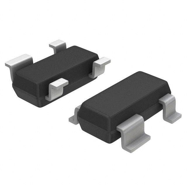
| 描述 | IC 10.8V SUPPLY MONITOR 8-SOIC监控电路 10.8V Monitor |
| 产品分类 | |
| 品牌 | Texas Instruments |
| 产品手册 | |
| 产品图片 |
|
| rohs | 符合RoHS无铅 / 符合限制有害物质指令(RoHS)规范要求 |
| 产品系列 | 电源管理 IC,监控电路,Texas Instruments TL7712ACD- |
| NumberofInputsMonitored | 1 Input |
| 数据手册 | |
| 产品型号 | TL7712ACD |
| 产品目录页面 | |
| 产品种类 | 监控电路 |
| 人工复位 | Manual Reset |
| 供应商器件封装 | 8-SOIC |
| 其它名称 | 296-3249-5 |
| 功率失效检测 | No |
| 包装 | 管件 |
| 单位重量 | 72.600 mg |
| 受监控电压数 | 1 |
| 商标 | Texas Instruments |
| 复位 | 高有效/低有效 |
| 复位超时 | 最大传输延迟为 1 µs |
| 安装类型 | 表面贴装 |
| 安装风格 | SMD/SMT |
| 封装 | Tube |
| 封装/外壳 | 8-SOIC(0.154",3.90mm 宽) |
| 封装/箱体 | SOIC-8 |
| 工作温度 | 0°C ~ 70°C |
| 工作电源电流 | 1.8 mA |
| 工厂包装数量 | 75 |
| 最大工作温度 | + 70 C |
| 最小工作温度 | 0 C |
| 标准包装 | 75 |
| 欠电压阈值 | 10.6 V |
| 电压-阈值 | 10.8V |
| 电池备用开关 | No Backup |
| 电源电压-最大 | 18 V |
| 电源电压-最小 | 3.5 V |
| 监视器 | No Watchdog |
| 类型 | 简单复位/加电复位 |
| 系列 | TL7712A |
| 芯片启用信号 | No Chip Enable |
| 被监测输入数 | 1 Input |
| 输出 | 补充型 |
| 输出类型 | Active High, Active Low, Open Drain |
| 过电压阈值 | 11 V |
| 重置延迟时间 | Programmable |
| 阈值电压 | 10.8 V |


- 商务部:美国ITC正式对集成电路等产品启动337调查
- 曝三星4nm工艺存在良率问题 高通将骁龙8 Gen1或转产台积电
- 太阳诱电将投资9.5亿元在常州建新厂生产MLCC 预计2023年完工
- 英特尔发布欧洲新工厂建设计划 深化IDM 2.0 战略
- 台积电先进制程称霸业界 有大客户加持明年业绩稳了
- 达到5530亿美元!SIA预计今年全球半导体销售额将创下新高
- 英特尔拟将自动驾驶子公司Mobileye上市 估值或超500亿美元
- 三星加码芯片和SET,合并消费电子和移动部门,撤换高东真等 CEO
- 三星电子宣布重大人事变动 还合并消费电子和移动部门
- 海关总署:前11个月进口集成电路产品价值2.52万亿元 增长14.8%


PDF Datasheet 数据手册内容提取
Product Sample & Technical Tools & Support & Folder Buy Documents Software Community TL7702A,TL7705A,TL7709A,TL7712A,TL7715A SLVS028K–APRIL1983–REVISEDSEPTEMBER2016 TL77xxA Supply-Voltage Supervisors 1 Features 3 Description • Power-OnResetGenerator The TL77xxA family of integrated-circuit supply- 1 voltage supervisors is designed specifically for use as • AutomaticResetGenerationAfterVoltageDrop reset controllers in microcomputer and • WideSupply-VoltageRange microprocessor systems. The supply-voltage • PrecisionVoltageSensor supervisor monitors the supply for undervoltage conditions at the SENSE input. During power up, the • Temperature-CompensatedVoltageReference RESET output becomes active (low) when V CC • ExternallyAdjustablePulseDuration attains a value approaching 3.6 V. At this point (assuming that SENSE is above V ), the delay timer IT+ 2 Applications function activates a time delay, after which outputs RESET and RESET go inactive (high and low, • Computers respectively). When an undervoltage condition occurs • Tablets during normal operation, RESET and RESET go • SmartPhones active. • Servers DeviceInformation(1) • MusicPlayers PARTNUMBER PACKAGE BODYSIZE(NOM) SOIC(8) 4.90mm×3.91mm TL77xxA PDIP(8) 9.81mm×6.35mm TL7705A SO(8) 6.20mm×5.30mm (1) For all available packages, see the orderable addendum at theendofthedatasheet. Three-SupplyMonitoring 1 An IMPORTANT NOTICE at the end of this data sheet addresses availability, warranty, changes, use in safety-critical applications, intellectualpropertymattersandotherimportantdisclaimers.PRODUCTIONDATA.
TL7702A,TL7705A,TL7709A,TL7712A,TL7715A SLVS028K–APRIL1983–REVISEDSEPTEMBER2016 www.ti.com Table of Contents 1 Features.................................................................. 1 8.4 DeviceFunctionalModes..........................................9 2 Applications........................................................... 1 9 ApplicationandImplementation........................ 10 3 Description............................................................. 1 9.1 ApplicationInformation............................................10 4 RevisionHistory..................................................... 2 9.2 TypicalApplication..................................................10 9.3 SystemExamples...................................................12 5 PinConfigurationandFunctions......................... 3 10 PowerSupplyRecommendations..................... 14 6 Specifications......................................................... 4 11 Layout................................................................... 14 6.1 AbsoluteMaximumRatings......................................4 6.2 ESDRatings..............................................................4 11.1 LayoutGuidelines.................................................14 6.3 RecommendedOperatingConditions.......................4 11.2 LayoutExample....................................................14 6.4 ThermalInformation..................................................5 12 DeviceandDocumentationSupport................. 15 6.5 ElectricalCharacteristics...........................................5 12.1 RelatedLinks........................................................15 6.6 SwitchingCharacteristics..........................................5 12.2 ReceivingNotificationofDocumentationUpdates15 6.7 TypicalCharacteristics..............................................6 12.3 CommunityResources..........................................15 7 ParameterMeasurementInformation..................7 12.4 Trademarks...........................................................15 12.5 ElectrostaticDischargeCaution............................15 8 DetailedDescription.............................................. 8 12.6 Glossary................................................................15 8.1 Overview...................................................................8 13 Mechanical,Packaging,andOrderable 8.2 FunctionalBlockDiagram.........................................8 Information........................................................... 15 8.3 FeatureDescription...................................................9 4 Revision History NOTE:Pagenumbersforpreviousrevisionsmaydifferfrompagenumbersinthecurrentversion. ChangesfromRevisionJ(January2015)toRevisionK Page • AddedSO(8)toDeviceInformationtable.............................................................................................................................. 1 • ChangedRESETtoRESETinTimingDiagram..................................................................................................................... 6 • AddedReceivingNotificationofDocumentationUpdatessection....................................................................................... 15 ChangesfromRevisionI(July2009)toRevisionJ Page • AddedApplications,DeviceInformationtable,PinFunctionstable,ESDRatingstable,ThermalInformationtable, TypicalCharacteristics,FeatureDescriptionsection,DeviceFunctionalModes,ApplicationandImplementation section,PowerSupplyRecommendationssection,Layoutsection,DeviceandDocumentationSupportsection,and Mechanical,Packaging,andOrderableInformationsection.................................................................................................. 1 • DeletedOrderingInformationtable........................................................................................................................................ 1 2 SubmitDocumentationFeedback Copyright©1983–2016,TexasInstrumentsIncorporated ProductFolderLinks:TL7702A TL7705A TL7709A TL7712A TL7715A
TL7702A,TL7705A,TL7709A,TL7712A,TL7715A www.ti.com SLVS028K–APRIL1983–REVISEDSEPTEMBER2016 5 Pin Configuration and Functions TL7702A,TL7709A,TL77012A,TL7715ADorPPackage TL7705AD,P,orPSPackage 8-PinSOIC,PDIP,orSO TopView REF 1 8 VCC RESIN 2 7 SENSE CT 3 6 RESET GND 4 5 RESET Not to scale PinFunctions PIN TYPE DESCRIPTION NAME NO. CT 3 I/O Externaltiming-capacitorpin GND 4 — Deviceground REF 1 O Voltagereferenceoutput RESET 6 O Supervisorresetsignaloutput RESET 5 O Supervisorresetsignaloutput(inverted) RESIN 2 I Resetinput SENSE 7 I Senseinput V 8 — PowerSupply CC Copyright©1983–2016,TexasInstrumentsIncorporated SubmitDocumentationFeedback 3 ProductFolderLinks:TL7702A TL7705A TL7709A TL7712A TL7715A
TL7702A,TL7705A,TL7709A,TL7712A,TL7715A SLVS028K–APRIL1983–REVISEDSEPTEMBER2016 www.ti.com 6 Specifications 6.1 Absolute Maximum Ratings overoperatingfree-airtemperaturerange(unlessotherwisenoted) (1) MIN MAX UNIT V Supplyvoltage(2) 20 V CC V Inputvoltage,RESIN –0.3 20 V I TL7702A(3) –0.3 6 V TL7705A –0.3 20 V V InputvoltagerangeSENSE I TL7709A –0.3 20 V TL7712A,TL7715A –0.3 20 V I High-leveloutputcurrent,I ,RESET –30 mA OH OH I Low-leveloutputcurrent,I ,RESET 30 mA OL OL T Operatingvirtualjunctiontemperature 150 °C J T Storagetemperature –65 150 °C stg (1) StressesbeyondthoselistedunderAbsoluteMaximumRatingsmaycausepermanentdamagetothedevice.Thesearestressratings only,whichdonotimplyfunctionaloperationofthedeviceattheseoranyotherconditionsbeyondthoseindicatedunderRecommended OperatingConditions.Exposuretoabsolute-maximum-ratedconditionsforextendedperiodsmayaffectdevicereliability. (2) ForproperoperationoftheTL7702A,thevoltageappliedtotheSENSEterminalshouldnotexceedV −1Vor6V,whicheverisless CC (3) AllvoltagevaluesarewithrespecttoGND. 6.2 ESD Ratings VALUE UNIT Humanbodymodel(HBM),perANSI/ESDA/JEDECJS-001(1) 1000 V Electrostaticdischarge V (ESD) Chargeddevicemodel(CDM),perJEDECspecificationJESD22-C101(2) 1000 (1) JEDECdocumentJEP155statesthat500-VHBMallowssafemanufacturingwithastandardESDcontrolprocess. (2) JEDECdocumentJEP157statesthat250-VCDMallowssafemanufacturingwithastandardESDcontrolprocess. 6.3 Recommended Operating Conditions overoperatingfree-airtemperaturerange(unlessotherwisenoted) MIN MAX UNIT V SupplyVoltage 3.5 18 V CC V High-levelinputvoltageatRESIN 2 V IH V Low-levelinputvoltageatRESIN 0.6 V IL TL7702A 0 See(1) TL7705A 0 10 V Inputvoltage,SENSE TL7709A 0 15 V I TL7712A 0 20 TL7715A 0 20 I High-leveloutputcurrent,RESET –16 mA OH I Low-leveloutputcurrent,RESET 16 mA OL TL77xxAC 0 70 T Operatingfree-airtemperature °C A TL77xxAI –40 85 (1) ForproperoperationoftheTL7702A,thevoltageappliedtotheSENSEterminalshouldnotexceedV −1Vor6V,whicheverisless. CC 4 SubmitDocumentationFeedback Copyright©1983–2016,TexasInstrumentsIncorporated ProductFolderLinks:TL7702A TL7705A TL7709A TL7712A TL7715A
TL7702A,TL7705A,TL7709A,TL7712A,TL7715A www.ti.com SLVS028K–APRIL1983–REVISEDSEPTEMBER2016 6.4 Thermal Information TL77xxA THERMALMETRIC(1) D P PS UNIT 8PINS 8PINS 8PINS R Junction-to-ambientthermalresistance 97 85 95 °C/W θJA (1) Formoreinformationabouttraditionalandnewthermalmetrics,seetheSemiconductorandICPackageThermalMetricsapplication report. 6.5 Electrical Characteristics overoperatingfree-airtemperaturerange(unlessotherwisenoted) TL77xxAC PARAMETER TESTCONDITIONS(1) TL77xxAI UNIT MIN TYP MAX VOH High-leveloutputvoltage,RESET IOH=–16mA VCC–1.5 V VOL Low-leveloutputvoltage,RESET IOL=16mA 0.4 V Vref ReferenceVoltage TA=25°C 2.48 2.53 2.58 V TL7702A 2.48 2.53 2.58 TL7705A 4.5 4.55 4.6 Negative-goinginput VIT– thresholdvoltage,SENSE TL7709A TA=25°C 7.5 7.6 7.7 V TL7712A 10.6 10.8 11 TL7715A 13.2 13.5 13.8 TL7702A 10 TL7705A 15 Vhys HVIyTs–)teresis,SENS(VIT+– TL7709A TA=25°C 20 mV TL7712A 35 TL7715A 45 VI=2.4VtoVCC 20 RESIN II Inputcurrent VI=0.4V –100 µA SENSE TL7702A Vref<VI<VCC–1.5V 0.5 2 IOH High-leveloutputcurrent,RESET VO=18V 50 µA IOL Low-leveloutputcurrent,RESET VO=0 –50 µA ICC Supplycurrent Allinputsandoutputsopen 1.8 3 mA (1) Allelectricalcharacteristicsaremeasuredwith0.1-µFcapacitorsconnectedatREF,CT,andV toGND. CC 6.6 Switching Characteristics overoperatingfree-airtemperaturerange(unlessotherwisenoted) TL77xxAC PARAMETER TESTCONDITIONS(1) TL77xxAI UNIT MIN TYP MAX Outputpulseduration CT=0.1µF 0.65 1.2 2.6 msec InputpulsedurationatRESIN 0.4 µs tw(S) Pouutlpseutsdurationatsenseinputtoswitch VmIVH=VIT−+200mV,VIL=VIT−−200 2 µs tpd propagationdelaytime,RESINtoRESET VCC=5V 1 µs RESET 0.2 tr Risetime VCC=5V(2) µs RESET 3.5 RESET 3.5 tf Falltime VCC=5V(2) µs RESET 0.2 (1) Allswitchingcharacteristicsaremeasuredwith0.1-µFcapacitorsconnectedatREFandV toGND. CC (2) Theriseandfalltimesaremeasuredwitha4.7-kΩloadresistoratRESETandRESET. Copyright©1983–2016,TexasInstrumentsIncorporated SubmitDocumentationFeedback 5 ProductFolderLinks:TL7702A TL7705A TL7709A TL7712A TL7715A
TL7702A,TL7705A,TL7709A,TL7712A,TL7715A SLVS028K–APRIL1983–REVISEDSEPTEMBER2016 www.ti.com VCC and SENSE Threshold Voltage VCC~ 3.6 V VCC~ 2 V RESET td td Output Undefined Output Undefined Figure1. TimingDiagram 6.7 Typical Characteristics Figure2.AssertionTimevsLoadResistance Figure3.DeassertionTimevsLoadResistance Figure4.AssertionTimevsLoadCapacitance Figure5.De-assertionTimevsLoadCapacitance 6 SubmitDocumentationFeedback Copyright©1983–2016,TexasInstrumentsIncorporated ProductFolderLinks:TL7702A TL7705A TL7709A TL7712A TL7715A
TL7702A,TL7705A,TL7709A,TL7712A,TL7715A www.ti.com SLVS028K–APRIL1983–REVISEDSEPTEMBER2016 7 Parameter Measurement Information Figure6. VoltageWaveform Copyright©1983–2016,TexasInstrumentsIncorporated SubmitDocumentationFeedback 7 ProductFolderLinks:TL7702A TL7705A TL7709A TL7712A TL7715A
TL7702A,TL7705A,TL7709A,TL7712A,TL7715A SLVS028K–APRIL1983–REVISEDSEPTEMBER2016 www.ti.com 8 Detailed Description 8.1 Overview The TL77xxA family of integrated-circuit supply-voltage supervisors is designed specifically for use as reset controllers in microcomputer and microprocessor systems. The supply-voltage supervisor monitors the supply for undervoltage conditions at the SENSE input. During power up, the RESET output becomes active (low) when V attains a value approaching 3.6 V. At this point (assuming that SENSE is above V ), the delay timer CC IT+ function activates a time delay, after which outputs RESET and RESET go inactive (high and low, respectively). Whenanundervoltageconditionoccursduringnormaloperation, RESETandRESETgoactive.Toensurethata complete reset occurs, the reset outputs remain active for a time delay after the voltage at the SENSE input exceedsthepositive-goingthresholdvalue. During power down and when SENSE is below V , the outputs remain active until V falls below 2 V. After IT− CC this, the outputs are undefined. An external capacitor (typically 0.1 μF) must be connected to REF to reduce the influenceoffasttransientsinthesupplyvoltage. Fiveversionsofthiscircuitareavailable: • TL7705A (Vt = 4.55 V): Application in TTL-systems and microcomputer systems which require a 5 volt supply (forexample,TMS7000) • TL7709A(Vt=7.6V):ApplicationinmicrocomputersystemsusingtheTMS1XXXNLL • TL7712A(Vt=10.8V):ApplicationinCMOS,microprocessor,andmemorycircuitswitha12voltsupply. • TL7715A(Vt=13.5V):Applicationincircuitswhichoperatewithasupplyvoltageof15V,asisfoundoftenin analogcircuits. • TL7702A(Vt=2.5V):Applicationinsystemswhereothersupplyvoltagesareused.Therequiredtriggerlevel mybeadjustedwithanexternalresistordividerattheSENSEinput. 8.2 Functional Block Diagram The functional block diagram is shown for illustrative purposes only; the actual circuit includes a trimming networktoadjustthereferencevoltageandsense-comparatortrippoint. ~100 µA A. TL7702A:R1=0Ω,R2=open TL7705A:R1=7.8kΩ,R2=10kΩ TL7709A:R1=19.7kΩ,R2=10kΩ TL7712A:R1=32.7kΩ,R2=10kΩ TL7715A:R1=43.4kΩ,R2=10kΩ B. Resistorvaluesshownarenominal. 8 SubmitDocumentationFeedback Copyright©1983–2016,TexasInstrumentsIncorporated ProductFolderLinks:TL7702A TL7705A TL7709A TL7712A TL7715A
TL7702A,TL7705A,TL7709A,TL7712A,TL7715A www.ti.com SLVS028K–APRIL1983–REVISEDSEPTEMBER2016 8.3 Feature Description 8.3.1 WideSupply-VoltageRange ThTL77xxAfamilyoperatesofawidesupplyvoltagerangeof3.5Vto18V. 8.3.2 ExternallyAdjustablePulseDuration The time delay is determined by the value of the external capacitor C : t = 1.3 × 10⁴ × C , where C is in farads T d T T (F)andt isinseconds(s). d 8.3.3 Temperature-CompensatedVoltageReference The series TL77xxA incorporates an extremely stable reference voltage source. This voltage source can also be used in applications where a constant voltage source is required. The reference voltage varies less than 10 mV over the supply voltage range of 3.5 V to 18 V. The same stability of the reference voltage is maintained, when theambienttemperatureischanged.Thereference'svoltagevariesonly16mVwhentheambienttemperatureis changedfrom–40°Cto+85°C. 8.4 Device Functional Modes Figure 7 shows the timing of the various signals. In this example the SENSE input is connected to the supply voltage V as in typical applications of this device. The minimum supply voltage for which the function of this CC device is guaranteed is 3.6 V. After power-on, the outputs are undefined until the minimum supply voltage V is res reached. For the TL77xxA the minimum supply voltage is V = 3 V (typical 2.5 V). Beyond the voltage V the res res capacitor C is first kept discharged, and the outputs stay in the active state (RESET = High, RESET = Low). T When the input voltage becomes higher than the threshold voltage V, the thyristor is turned off and the capacitor t ischarged.Afteradelay,t ,thevoltageatthecapacitorpassesthetriggerleveloftheoutputcomparatorandthe d outputsbecomeinactive.Thecircuittobeinitializedisnowsettoadefinedstateandstartsthecorrectoperation. A. Note:SENSEInputconnectedtoV CC Figure7. TimingDiagram Copyright©1983–2016,TexasInstrumentsIncorporated SubmitDocumentationFeedback 9 ProductFolderLinks:TL7702A TL7705A TL7709A TL7712A TL7715A
TL7702A,TL7705A,TL7709A,TL7712A,TL7715A SLVS028K–APRIL1983–REVISEDSEPTEMBER2016 www.ti.com 9 Application and Implementation NOTE Information in the following applications sections is not part of the TI component specification, and TI does not warrant its accuracy or completeness. TI’s customers are responsible for determining suitability of components for their purposes. Customers should validateandtesttheirdesignimplementationtoconfirmsystemfunctionality. 9.1 Application Information This application shows the initialization circuit diagrams for a microprocessor system with supply voltage Vcc = 5 V. The external components required are the decoupling capacitor C for the reference voltage and the timing ref capacitor C . The outputs of the TL77xxA are open collector outputs. In Figure 8 therefore a pull-up resistor is T shownattheRESEToutputtoensurethecorrectHIGHlevel. 9.2 Typical Application µC = Figure8. ResetControllerSchematicforaMicroprocessor 9.2.1 DesignRequirements • 5-Vmicroprocessorsupplyvoltage • t =1.3ms d 9.2.2 DetailedDesignProcedure • Selectreasonablevaluesforpull-up/pull-downresistorsforRESETand RESET.Thisdesignuses10kΩ. • ChooseC =0.1µFtoachievet =1.3ms T d • This design uses only the active-low reset output (RESET) because the example microcontroller resets when theinputisLow. 10 SubmitDocumentationFeedback Copyright©1983–2016,TexasInstrumentsIncorporated ProductFolderLinks:TL7702A TL7705A TL7709A TL7712A TL7715A
TL7702A,TL7705A,TL7709A,TL7712A,TL7715A www.ti.com SLVS028K–APRIL1983–REVISEDSEPTEMBER2016 Typical Application (continued) 9.2.3 ApplicationCurves 5 5 4.5 4.5 4 4 V) 3.5 V) 3.5 ge ( 3 ge ( 3 a a olt 2.5 olt 2.5 V V T T E 2 E 2 S S E E R 1.5 R 1.5 1 1 0.5 0.5 0 0 0 0.5 1 1.5 2 2.5 3 3.5 4 4.5 5 0 0.5 1 1.5 2 2.5 3 3.5 4 4.5 5 VCC (V) VCC (V) D005 D006 Figure9.SupervisorRESETOutputVoltagevsV Figure10.SupervisorRESETOutputVoltagevsV CC CC 5 5 4.5 4.5 4 4 V) 3.5 V) 3.5 ge ( 3 ge ( 3 a a olt 2.5 olt 2.5 V V T T E 2 E 2 S S E E R 1.5 R 1.5 1 1 0.5 0.5 0 0 4.5 4.52 4.54 4.56 4.58 4.6 4.5 4.52 4.54 4.56 4.58 4.6 VCC (V) VCC (V) D007 D008 Figure11.SupervisorRESETOutputVoltagevsV at Figure12.SupervisorRESETOutputVoltagevsV at CC CC Transition Transition Copyright©1983–2016,TexasInstrumentsIncorporated SubmitDocumentationFeedback 11 ProductFolderLinks:TL7702A TL7705A TL7709A TL7712A TL7715A
TL7702A,TL7705A,TL7709A,TL7712A,TL7715A SLVS028K–APRIL1983–REVISEDSEPTEMBER2016 www.ti.com 9.3 System Examples Figure13. MultiPower-SupplySystemResetGenerationSchematic Figure14. EliminatingUndefinedStatesUsingaP-ChannelJFETSchematic 12 SubmitDocumentationFeedback Copyright©1983–2016,TexasInstrumentsIncorporated ProductFolderLinks:TL7702A TL7705A TL7709A TL7712A TL7715A
TL7702A,TL7705A,TL7709A,TL7712A,TL7715A www.ti.com SLVS028K–APRIL1983–REVISEDSEPTEMBER2016 System Examples (continued) Figure15. EliminatingUndefinedStatesUsingPNPTransistorSchematic Copyright©1983–2016,TexasInstrumentsIncorporated SubmitDocumentationFeedback 13 ProductFolderLinks:TL7702A TL7705A TL7709A TL7712A TL7715A
TL7702A,TL7705A,TL7709A,TL7712A,TL7715A SLVS028K–APRIL1983–REVISEDSEPTEMBER2016 www.ti.com 10 Power Supply Recommendations The TL77xxA devices operate within the specifications from the Recommended Operating Conditions between 3.5Vand18V. CAUTION Thesedevicesriskbeingdamagedwhenpoweredbymorethan20V. 11 Layout 11.1 Layout Guidelines The voltage monitor should be placed on the printed circuit board, where there are no neighboring circuits in the which switch high currents (like bus interface circuits and power switches). When laying out the layout of the printed circuit board, take special care with the interconnects which carry analog signals. Beside the SENSE input these are the C and V terminals. Noise coupled into the C input will lead to a reduction of the output T ref T pulse width. Noise coupled into the V input or into the filter capacitor at this input may lead to undesired ref triggeringofthecircuitandbythistoanundesiredRESETpulse.Practiceshows,thatthismalfunctionwhenhigh currents flow over the interconnects of these capacitors to the GND terminal of the voltage monitor. To avoid theseeffects,theGNDterminalsofthesecapacitorsmustbeconnectedbytheshortestwaytotheGNDterminal of the voltage monitor in so that no currents caused by other circuits flow over these wires. Figure 16 show a layout proposal for the printed circuit board. Furthermore the resistors of the voltage divider at the SENSE input oftheTL7702(R2andR3inFigure16)havetobeplacedinso,thatnonoisemaybecoupledintothiscircuit. 11.2 Layout Example 1 8 2 7 3 6 4 5 Figure16. PrintedCircuitLayoutfortheSupplyVoltageSupervisor 14 SubmitDocumentationFeedback Copyright©1983–2016,TexasInstrumentsIncorporated ProductFolderLinks:TL7702A TL7705A TL7709A TL7712A TL7715A
TL7702A,TL7705A,TL7709A,TL7712A,TL7715A www.ti.com SLVS028K–APRIL1983–REVISEDSEPTEMBER2016 12 Device and Documentation Support 12.1 Related Links The table below lists quick access links. Categories include technical documents, support and community resources,toolsandsoftware,andquickaccesstosampleorbuy. Table1.RelatedLinks TECHNICAL TOOLS& SUPPORT& PARTS PRODUCTFOLDER SAMPLE&BUY DOCUMENTS SOFTWARE COMMUNITY TL7702A Clickhere Clickhere Clickhere Clickhere Clickhere TL7705A Clickhere Clickhere Clickhere Clickhere Clickhere TL7709A Clickhere Clickhere Clickhere Clickhere Clickhere TL7712A Clickhere Clickhere Clickhere Clickhere Clickhere TL7715A Clickhere Clickhere Clickhere Clickhere Clickhere 12.2 Receiving Notification of Documentation Updates To receive notification of documentation updates, navigate to the device product folder on ti.com. In the upper right corner, click on Alert me to register and receive a weekly digest of any product information that has changed.Forchangedetails,reviewtherevisionhistoryincludedinanyreviseddocument. 12.3 Community Resources The following links connect to TI community resources. Linked contents are provided "AS IS" by the respective contributors. They do not constitute TI specifications and do not necessarily reflect TI's views; see TI's Terms of Use. TIE2E™OnlineCommunity TI'sEngineer-to-Engineer(E2E)Community.Createdtofostercollaboration amongengineers.Ate2e.ti.com,youcanaskquestions,shareknowledge,exploreideasandhelp solveproblemswithfellowengineers. DesignSupport TI'sDesignSupport QuicklyfindhelpfulE2Eforumsalongwithdesignsupporttoolsand contactinformationfortechnicalsupport. 12.4 Trademarks E2EisatrademarkofTexasInstruments. Allothertrademarksarethepropertyoftheirrespectiveowners. 12.5 Electrostatic Discharge Caution This integrated circuit can be damaged by ESD. Texas Instruments recommends that all integrated circuits be handled with appropriateprecautions.Failuretoobserveproperhandlingandinstallationprocedurescancausedamage. ESDdamagecanrangefromsubtleperformancedegradationtocompletedevicefailure.Precisionintegratedcircuitsmaybemore susceptibletodamagebecauseverysmallparametricchangescouldcausethedevicenottomeetitspublishedspecifications. 12.6 Glossary SLYZ022—TIGlossary. Thisglossarylistsandexplainsterms,acronyms,anddefinitions. 13 Mechanical, Packaging, and Orderable Information The following pages include mechanical, packaging, and orderable information. This information is the most current data available for the designated devices. This data is subject to change without notice and revision of thisdocument.Forbrowser-basedversionsofthisdatasheet,refertotheleft-handnavigation. Copyright©1983–2016,TexasInstrumentsIncorporated SubmitDocumentationFeedback 15 ProductFolderLinks:TL7702A TL7705A TL7709A TL7712A TL7715A
PACKAGE OPTION ADDENDUM www.ti.com 6-Feb-2020 PACKAGING INFORMATION Orderable Device Status Package Type Package Pins Package Eco Plan Lead/Ball Finish MSL Peak Temp Op Temp (°C) Device Marking Samples (1) Drawing Qty (2) (6) (3) (4/5) TL7702ACD ACTIVE SOIC D 8 75 Green (RoHS NIPDAU Level-1-260C-UNLIM 0 to 70 7702AC & no Sb/Br) TL7702ACDR ACTIVE SOIC D 8 2500 Green (RoHS NIPDAU Level-1-260C-UNLIM 0 to 70 7702AC & no Sb/Br) TL7702ACDRG4 ACTIVE SOIC D 8 2500 Green (RoHS NIPDAU Level-1-260C-UNLIM 0 to 70 7702AC & no Sb/Br) TL7702ACP ACTIVE PDIP P 8 50 Green (RoHS NIPDAU N / A for Pkg Type 0 to 70 TL7702ACP & no Sb/Br) TL7702AID ACTIVE SOIC D 8 75 Green (RoHS NIPDAU Level-1-260C-UNLIM -40 to 85 7702AI & no Sb/Br) TL7702AIDR ACTIVE SOIC D 8 2500 Green (RoHS NIPDAU Level-1-260C-UNLIM -40 to 85 7702AI & no Sb/Br) TL7702AIDRG4 ACTIVE SOIC D 8 2500 Green (RoHS NIPDAU Level-1-260C-UNLIM -40 to 85 7702AI & no Sb/Br) TL7702AIP ACTIVE PDIP P 8 50 Pb-Free NIPDAU N / A for Pkg Type -40 to 85 TL7702AIP (RoHS) TL7702AIPE4 ACTIVE PDIP P 8 50 Pb-Free NIPDAU N / A for Pkg Type -40 to 85 TL7702AIP (RoHS) TL7705ACD ACTIVE SOIC D 8 75 Green (RoHS NIPDAU Level-1-260C-UNLIM 0 to 70 7705AC & no Sb/Br) TL7705ACDE4 ACTIVE SOIC D 8 75 Green (RoHS NIPDAU Level-1-260C-UNLIM 0 to 70 7705AC & no Sb/Br) TL7705ACDG4 ACTIVE SOIC D 8 75 Green (RoHS NIPDAU Level-1-260C-UNLIM 0 to 70 7705AC & no Sb/Br) TL7705ACDR ACTIVE SOIC D 8 2500 Green (RoHS NIPDAU Level-1-260C-UNLIM 0 to 70 7705AC & no Sb/Br) TL7705ACDRG4 ACTIVE SOIC D 8 2500 Green (RoHS NIPDAU Level-1-260C-UNLIM 0 to 70 7705AC & no Sb/Br) TL7705ACP ACTIVE PDIP P 8 50 Green (RoHS NIPDAU N / A for Pkg Type 0 to 70 TL7705ACP & no Sb/Br) TL7705ACPE4 ACTIVE PDIP P 8 50 Green (RoHS NIPDAU N / A for Pkg Type 0 to 70 TL7705ACP & no Sb/Br) TL7705ACPSR ACTIVE SO PS 8 2000 Green (RoHS NIPDAU Level-1-260C-UNLIM 0 to 70 T7705A & no Sb/Br) Addendum-Page 1
PACKAGE OPTION ADDENDUM www.ti.com 6-Feb-2020 Orderable Device Status Package Type Package Pins Package Eco Plan Lead/Ball Finish MSL Peak Temp Op Temp (°C) Device Marking Samples (1) Drawing Qty (2) (6) (3) (4/5) TL7705AID ACTIVE SOIC D 8 75 Green (RoHS NIPDAU Level-1-260C-UNLIM -40 to 85 7705AI & no Sb/Br) TL7705AIDG4 ACTIVE SOIC D 8 75 Green (RoHS NIPDAU Level-1-260C-UNLIM -40 to 85 7705AI & no Sb/Br) TL7705AIDR ACTIVE SOIC D 8 2500 Green (RoHS NIPDAU Level-1-260C-UNLIM -40 to 85 7705AI & no Sb/Br) TL7705AIDRG4 ACTIVE SOIC D 8 2500 Green (RoHS NIPDAU Level-1-260C-UNLIM -40 to 85 7705AI & no Sb/Br) TL7705AIP ACTIVE PDIP P 8 50 Green (RoHS NIPDAU N / A for Pkg Type -40 to 85 TL7705AIP & no Sb/Br) TL7709ACD ACTIVE SOIC D 8 75 Green (RoHS NIPDAU Level-1-260C-UNLIM 0 to 70 7709AC & no Sb/Br) TL7709ACDG4 ACTIVE SOIC D 8 75 Green (RoHS NIPDAU Level-1-260C-UNLIM 0 to 70 7709AC & no Sb/Br) TL7709ACDR ACTIVE SOIC D 8 2500 Green (RoHS NIPDAU Level-1-260C-UNLIM 0 to 70 7709AC & no Sb/Br) TL7709ACP ACTIVE PDIP P 8 50 Green (RoHS NIPDAU N / A for Pkg Type 0 to 70 TL7709ACP & no Sb/Br) TL7712ACD ACTIVE SOIC D 8 75 Green (RoHS NIPDAU Level-1-260C-UNLIM 0 to 70 7712AC & no Sb/Br) TL7712ACDE4 ACTIVE SOIC D 8 75 Green (RoHS NIPDAU Level-1-260C-UNLIM 0 to 70 7712AC & no Sb/Br) TL7712ACDG4 ACTIVE SOIC D 8 75 Green (RoHS NIPDAU Level-1-260C-UNLIM 0 to 70 7712AC & no Sb/Br) TL7712ACDR ACTIVE SOIC D 8 2500 Green (RoHS NIPDAU Level-1-260C-UNLIM 0 to 70 7712AC & no Sb/Br) TL7712ACDRE4 ACTIVE SOIC D 8 2500 Green (RoHS NIPDAU Level-1-260C-UNLIM 0 to 70 7712AC & no Sb/Br) TL7712ACDRG4 ACTIVE SOIC D 8 2500 Green (RoHS NIPDAU Level-1-260C-UNLIM 0 to 70 7712AC & no Sb/Br) TL7712ACP ACTIVE PDIP P 8 50 Green (RoHS NIPDAU N / A for Pkg Type 0 to 70 TL7712ACP & no Sb/Br) TL7712AIDR ACTIVE SOIC D 8 2500 Green (RoHS NIPDAU Level-1-260C-UNLIM 7712AI & no Sb/Br) TL7715ACD ACTIVE SOIC D 8 75 Green (RoHS NIPDAU Level-1-260C-UNLIM 0 to 70 7715AC & no Sb/Br) Addendum-Page 2
PACKAGE OPTION ADDENDUM www.ti.com 6-Feb-2020 Orderable Device Status Package Type Package Pins Package Eco Plan Lead/Ball Finish MSL Peak Temp Op Temp (°C) Device Marking Samples (1) Drawing Qty (2) (6) (3) (4/5) TL7715ACDE4 ACTIVE SOIC D 8 75 Green (RoHS NIPDAU Level-1-260C-UNLIM 0 to 70 7715AC & no Sb/Br) TL7715ACP ACTIVE PDIP P 8 50 Green (RoHS NIPDAU N / A for Pkg Type 0 to 70 TL7715ACP & no Sb/Br) (1) The marketing status values are defined as follows: ACTIVE: Product device recommended for new designs. LIFEBUY: TI has announced that the device will be discontinued, and a lifetime-buy period is in effect. NRND: Not recommended for new designs. Device is in production to support existing customers, but TI does not recommend using this part in a new design. PREVIEW: Device has been announced but is not in production. Samples may or may not be available. OBSOLETE: TI has discontinued the production of the device. (2) RoHS: TI defines "RoHS" to mean semiconductor products that are compliant with the current EU RoHS requirements for all 10 RoHS substances, including the requirement that RoHS substance do not exceed 0.1% by weight in homogeneous materials. Where designed to be soldered at high temperatures, "RoHS" products are suitable for use in specified lead-free processes. TI may reference these types of products as "Pb-Free". RoHS Exempt: TI defines "RoHS Exempt" to mean products that contain lead but are compliant with EU RoHS pursuant to a specific EU RoHS exemption. Green: TI defines "Green" to mean the content of Chlorine (Cl) and Bromine (Br) based flame retardants meet JS709B low halogen requirements of <=1000ppm threshold. Antimony trioxide based flame retardants must also meet the <=1000ppm threshold requirement. (3) MSL, Peak Temp. - The Moisture Sensitivity Level rating according to the JEDEC industry standard classifications, and peak solder temperature. (4) There may be additional marking, which relates to the logo, the lot trace code information, or the environmental category on the device. (5) Multiple Device Markings will be inside parentheses. Only one Device Marking contained in parentheses and separated by a "~" will appear on a device. If a line is indented then it is a continuation of the previous line and the two combined represent the entire Device Marking for that device. (6) Lead/Ball Finish - Orderable Devices may have multiple material finish options. Finish options are separated by a vertical ruled line. Lead/Ball Finish values may wrap to two lines if the finish value exceeds the maximum column width. Important Information and Disclaimer:The information provided on this page represents TI's knowledge and belief as of the date that it is provided. TI bases its knowledge and belief on information provided by third parties, and makes no representation or warranty as to the accuracy of such information. Efforts are underway to better integrate information from third parties. TI has taken and continues to take reasonable steps to provide representative and accurate information but may not have conducted destructive testing or chemical analysis on incoming materials and chemicals. TI and TI suppliers consider certain information to be proprietary, and thus CAS numbers and other limited information may not be available for release. In no event shall TI's liability arising out of such information exceed the total purchase price of the TI part(s) at issue in this document sold by TI to Customer on an annual basis. Addendum-Page 3
PACKAGE MATERIALS INFORMATION www.ti.com 20-Dec-2018 TAPE AND REEL INFORMATION *Alldimensionsarenominal Device Package Package Pins SPQ Reel Reel A0 B0 K0 P1 W Pin1 Type Drawing Diameter Width (mm) (mm) (mm) (mm) (mm) Quadrant (mm) W1(mm) TL7702ACDR SOIC D 8 2500 330.0 12.4 6.4 5.2 2.1 8.0 12.0 Q1 TL7702ACDR SOIC D 8 2500 330.0 12.4 6.4 5.2 2.1 8.0 12.0 Q1 TL7702AIDR SOIC D 8 2500 330.0 12.4 6.4 5.2 2.1 8.0 12.0 Q1 TL7705ACDR SOIC D 8 2500 330.0 12.4 6.4 5.2 2.1 8.0 12.0 Q1 TL7705AIDR SOIC D 8 2500 330.0 12.4 6.4 5.2 2.1 8.0 12.0 Q1 TL7709ACDR SOIC D 8 2500 330.0 12.4 6.4 5.2 2.1 8.0 12.0 Q1 TL7712ACDR SOIC D 8 2500 330.0 12.4 6.4 5.2 2.1 8.0 12.0 Q1 TL7712AIDR SOIC D 8 2500 330.0 12.4 6.4 5.2 2.1 8.0 12.0 Q1 PackMaterials-Page1
PACKAGE MATERIALS INFORMATION www.ti.com 20-Dec-2018 *Alldimensionsarenominal Device PackageType PackageDrawing Pins SPQ Length(mm) Width(mm) Height(mm) TL7702ACDR SOIC D 8 2500 367.0 367.0 35.0 TL7702ACDR SOIC D 8 2500 340.5 338.1 20.6 TL7702AIDR SOIC D 8 2500 340.5 338.1 20.6 TL7705ACDR SOIC D 8 2500 340.5 338.1 20.6 TL7705AIDR SOIC D 8 2500 340.5 338.1 20.6 TL7709ACDR SOIC D 8 2500 340.5 338.1 20.6 TL7712ACDR SOIC D 8 2500 340.5 338.1 20.6 TL7712AIDR SOIC D 8 2500 340.5 338.1 20.6 PackMaterials-Page2
PACKAGE OUTLINE D0008A SOIC - 1.75 mm max height SCALE 2.800 SMALL OUTLINE INTEGRATED CIRCUIT C SEATING PLANE .228-.244 TYP [5.80-6.19] .004 [0.1] C A PIN 1 ID AREA 6X .050 [1.27] 8 1 2X .189-.197 [4.81-5.00] .150 NOTE 3 [3.81] 4X (0 -15 ) 4 5 8X .012-.020 B .150-.157 [0.31-0.51] .069 MAX [3.81-3.98] .010 [0.25] C A B [1.75] NOTE 4 .005-.010 TYP [0.13-0.25] 4X (0 -15 ) SEE DETAIL A .010 [0.25] .004-.010 0 - 8 [0.11-0.25] .016-.050 [0.41-1.27] DETAIL A (.041) TYPICAL [1.04] 4214825/C 02/2019 NOTES: 1. Linear dimensions are in inches [millimeters]. Dimensions in parenthesis are for reference only. Controlling dimensions are in inches. Dimensioning and tolerancing per ASME Y14.5M. 2. This drawing is subject to change without notice. 3. This dimension does not include mold flash, protrusions, or gate burrs. Mold flash, protrusions, or gate burrs shall not exceed .006 [0.15] per side. 4. This dimension does not include interlead flash. 5. Reference JEDEC registration MS-012, variation AA. www.ti.com
EXAMPLE BOARD LAYOUT D0008A SOIC - 1.75 mm max height SMALL OUTLINE INTEGRATED CIRCUIT 8X (.061 ) [1.55] SYMM SEE DETAILS 1 8 8X (.024) [0.6] SYMM (R.002 ) TYP [0.05] 5 4 6X (.050 ) [1.27] (.213) [5.4] LAND PATTERN EXAMPLE EXPOSED METAL SHOWN SCALE:8X SOLDER MASK SOLDER MASK METAL OPENING OPENING METAL UNDER SOLDER MASK EXPOSED METAL EXPOSED METAL .0028 MAX .0028 MIN [0.07] [0.07] ALL AROUND ALL AROUND NON SOLDER MASK SOLDER MASK DEFINED DEFINED SOLDER MASK DETAILS 4214825/C 02/2019 NOTES: (continued) 6. Publication IPC-7351 may have alternate designs. 7. Solder mask tolerances between and around signal pads can vary based on board fabrication site. www.ti.com
EXAMPLE STENCIL DESIGN D0008A SOIC - 1.75 mm max height SMALL OUTLINE INTEGRATED CIRCUIT 8X (.061 ) [1.55] SYMM 1 8 8X (.024) [0.6] SYMM (R.002 ) TYP [0.05] 5 4 6X (.050 ) [1.27] (.213) [5.4] SOLDER PASTE EXAMPLE BASED ON .005 INCH [0.125 MM] THICK STENCIL SCALE:8X 4214825/C 02/2019 NOTES: (continued) 8. Laser cutting apertures with trapezoidal walls and rounded corners may offer better paste release. IPC-7525 may have alternate design recommendations. 9. Board assembly site may have different recommendations for stencil design. www.ti.com
None
None
None
IMPORTANTNOTICEANDDISCLAIMER TI PROVIDES TECHNICAL AND RELIABILITY DATA (INCLUDING DATASHEETS), DESIGN RESOURCES (INCLUDING REFERENCE DESIGNS), APPLICATION OR OTHER DESIGN ADVICE, WEB TOOLS, SAFETY INFORMATION, AND OTHER RESOURCES “AS IS” AND WITH ALL FAULTS, AND DISCLAIMS ALL WARRANTIES, EXPRESS AND IMPLIED, INCLUDING WITHOUT LIMITATION ANY IMPLIED WARRANTIES OF MERCHANTABILITY, FITNESS FOR A PARTICULAR PURPOSE OR NON-INFRINGEMENT OF THIRD PARTY INTELLECTUAL PROPERTY RIGHTS. These resources are intended for skilled developers designing with TI products. You are solely responsible for (1) selecting the appropriate TI products for your application, (2) designing, validating and testing your application, and (3) ensuring your application meets applicable standards, and any other safety, security, or other requirements. These resources are subject to change without notice. TI grants you permission to use these resources only for development of an application that uses the TI products described in the resource. Other reproduction and display of these resources is prohibited. No license is granted to any other TI intellectual property right or to any third party intellectual property right. TI disclaims responsibility for, and you will fully indemnify TI and its representatives against, any claims, damages, costs, losses, and liabilities arising out of your use of these resources. TI’s products are provided subject to TI’s Terms of Sale (www.ti.com/legal/termsofsale.html) or other applicable terms available either on ti.com or provided in conjunction with such TI products. TI’s provision of these resources does not expand or otherwise alter TI’s applicable warranties or warranty disclaimers for TI products. Mailing Address: Texas Instruments, Post Office Box 655303, Dallas, Texas 75265 Copyright © 2020, Texas Instruments Incorporated