ICGOO在线商城 > 集成电路(IC) > PMIC - 监控器 > TPS3125J12DBVT
 Datasheet下载
- 型号: TPS3125J12DBVT
- 制造商: Texas Instruments
- 库位|库存: xxxx|xxxx
- 要求:
| 数量阶梯 | 香港交货 | 国内含税 |
| +xxxx | $xxxx | ¥xxxx |
查看当月历史价格
查看今年历史价格
TPS3125J12DBVT产品简介:
ICGOO电子元器件商城为您提供TPS3125J12DBVT由Texas Instruments设计生产,在icgoo商城现货销售,并且可以通过原厂、代理商等渠道进行代购。 TPS3125J12DBVT价格参考¥7.44-¥16.73。Texas InstrumentsTPS3125J12DBVT封装/规格:PMIC - 监控器, Supervisor Push-Pull, Totem Pole 1 Channel SOT-23-5。您可以下载TPS3125J12DBVT参考资料、Datasheet数据手册功能说明书,资料中有TPS3125J12DBVT 详细功能的应用电路图电压和使用方法及教程。
TPS3125J12DBVT是德州仪器(Texas Instruments)生产的一款电压监控器(PMIC - 监控器),主要用于对系统电源电压进行实时监测,确保电子系统的稳定运行。其典型应用场景包括便携式设备、电池供电系统、嵌入式系统和工业控制设备等。

该器件集成了固定阈值的电压检测功能,复位阈值为1.2V,适用于低电压供电环境。当电源电压低于设定阈值时,TPS3125J12DBVT会输出复位信号,使微控制器或处理器进入复位状态,防止因电压过低导致系统运行异常或数据损坏。待电压恢复至正常范围并保持一段时间后,复位信号解除,系统重新启动,保障上电过程的可靠性。

由于采用小型SOT-23封装(DBVT),该芯片占用空间小,功耗低,非常适合对尺寸和功耗敏感的应用,如可穿戴设备、物联网终端、智能家居传感器等。此外,其高精度检测和快速响应特性也使其广泛应用于通信模块、医疗电子设备和汽车电子中的辅助控制单元。

综上所述,TPS3125J12DBVT是一款高性能、小体积的电压监控器,适用于需要可靠电源管理的各种低功耗、高稳定性电子系统。
| 参数 | 数值 |
| 产品目录 | 集成电路 (IC)半导体 |
| 描述 | IC 1.08V SUPPLY MONITOR SOT23-5监控电路 Ultra-Low Voltage Processor |
| 产品分类 | |
| 品牌 | Texas Instruments |
| 产品手册 | |
| 产品图片 |
|
| rohs | 符合RoHS无铅 / 符合限制有害物质指令(RoHS)规范要求 |
| 产品系列 | 电源管理 IC,监控电路,Texas Instruments TPS3125J12DBVT- |
| NumberofInputsMonitored | 1 Input |
| 数据手册 | |
| 产品型号 | TPS3125J12DBVT |
| 产品目录页面 | |
| 产品种类 | 监控电路 |
| 人工复位 | Manual Reset |
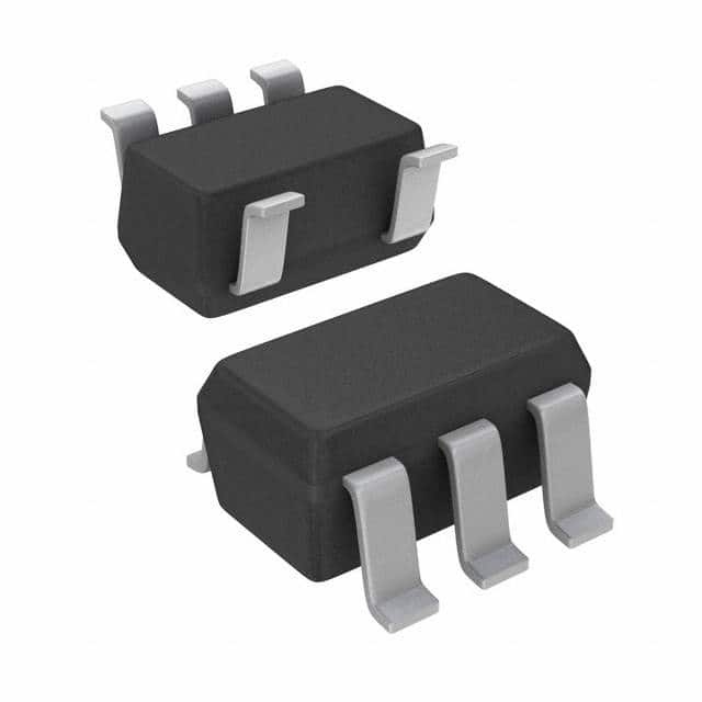
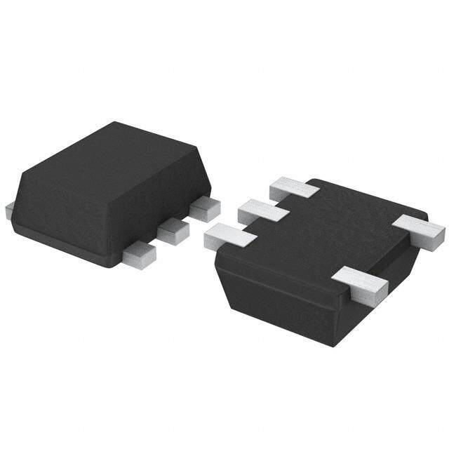
| 供应商器件封装 | SOT-23-5 |
| 其它名称 | 296-2614-2 |
| 功率失效检测 | No |
| 包装 | 带卷 (TR) |
| 单位重量 | 13 mg |
| 受监控电压数 | 1 |
| 商标 | Texas Instruments |
| 复位 | 高有效/低有效 |
| 复位超时 | 最小为 100 ms |
| 安装类型 | 表面贴装 |
| 安装风格 | SMD/SMT |
| 封装 | Reel |
| 封装/外壳 | SC-74A,SOT-753 |
| 封装/箱体 | SOT-23-5 |
| 工作温度 | -40°C ~ 85°C |
| 工作电源电流 | 14 uA |
| 工厂包装数量 | 250 |
| 最大功率耗散 | 437 mW |
| 最大工作温度 | + 85 C |
| 最小工作温度 | - 40 C |
| 标准包装 | 250 |
| 欠电压阈值 | 1.08 V |
| 电压-阈值 | 1.08V |
| 电池备用开关 | No Backup |
| 电源电压-最大 | 3.3 V |
| 电源电压-最小 | 0.75 V |
| 监视器 | No Watchdog |
| 类型 | 简单复位/加电复位 |
| 系列 | TPS3125J12 |
| 芯片启用信号 | No Chip Enable |
| 被监测输入数 | 1 Input |
| 输出 | 推挽式,图腾柱 |
| 输出类型 | Push-Pull |
| 过电压阈值 | 1.12 V |
| 重置延迟时间 | 180 ms |
| 阈值电压 | 0.85 V to 3.3 V |


- 商务部:美国ITC正式对集成电路等产品启动337调查
- 曝三星4nm工艺存在良率问题 高通将骁龙8 Gen1或转产台积电
- 太阳诱电将投资9.5亿元在常州建新厂生产MLCC 预计2023年完工
- 英特尔发布欧洲新工厂建设计划 深化IDM 2.0 战略
- 台积电先进制程称霸业界 有大客户加持明年业绩稳了
- 达到5530亿美元!SIA预计今年全球半导体销售额将创下新高
- 英特尔拟将自动驾驶子公司Mobileye上市 估值或超500亿美元
- 三星加码芯片和SET,合并消费电子和移动部门,撤换高东真等 CEO
- 三星电子宣布重大人事变动 还合并消费电子和移动部门
- 海关总署:前11个月进口集成电路产品价值2.52万亿元 增长14.8%


PDF Datasheet 数据手册内容提取
TPS3123-xx TPS3124-xx, TPS3125-xx TPS3126-xx, TPS3128-xx www.ti.com SLVS227B–AUGUST1999–REVISEDFEBRUARY2004 ULTRA-LOW VOLTAGE PROCESSOR SUPERVISORY CIRCUITS FEATURES DBV PACKAGE • MinimumSupplyVoltageof0.75V (TOP VIEW) • SupplyVoltageSupervisionRange: TPS3123/T – 1.2V,1.5V,1.8V(TPS312x) PS3128 – 3V(TPS3125DevicesOnly) RESET 1 5 VDD – OtherVersionsonRequest • Power-OnResetGeneratorWithFixedDelay GND 2 Timeof180ms MR 3 4 WDI • ManualResetInput(TPS3123/5/6/8) • WatchdogTimerRetriggerstheRESETOutput TPS3124 atV ‡ V DD IT • SupplyCurrentof14µA(Typ) RESET 1 5 VDD • SmallSOT23-5Package GND 2 • TemperatureRangeof -40(cid:176)C to85(cid:176)C • ResetOutputAvailableinPush-Pull(Active RESET 3 4 WDI LowandHigh)andOpen-Drain(Active-Low) TPS3125/ APPLICATIONS TPS3126 • ApplicationsUsingLowVoltageDSPs, RESET 1 5 VDD Microcontrollers,orMicroprocessors • Portable/Battery-PoweredEquipment GND 2 • WirelessCommunicationSystems • ProgrammableControls RESET 3 4 MR • IndustrialEquipment • Notebook/DesktopComputers • IntelligentInstruments 1.2 V CVDD DVDD TMS320UVC5402 VDD RESET RESET MR WDI XF GND TPS3123J12 GND Figure1.TypicalLow-VoltageDSPApplication Pleasebeawarethatanimportantnoticeconcerningavailability,standardwarranty,anduseincriticalapplicationsofTexas Instrumentssemiconductorproductsanddisclaimerstheretoappearsattheendofthisdatasheet. PRODUCTIONDATAinformationiscurrentasofpublicationdate. Copyright©1999–2004,TexasInstrumentsIncorporated Products conform to specifications per the terms of the Texas Instruments standard warranty. Production processing does not necessarilyincludetestingofallparameters.
TPS3123-xx TPS3124-xx, TPS3125-xx TPS3126-xx, TPS3128-xx www.ti.com SLVS227B–AUGUST1999–REVISEDFEBRUARY2004 DESCRIPTION The TPS312x family of ultralow voltage processor supervisory circuits provides circuit initialization and timing supervision,primarilyforDSPandprocessor-basedsystems. Duringpower-on,RESETisasserted when the supply voltage (V ) becomes higher than 0.75 V. Thereafter, the DD supply voltage supervisor monitors V and keeps RESET output active as long as V remains below the DD DD threshold voltage (V ). An internal timer delays the return of the output to the inactive state (high) to ensure IT propersystemreset.Thedelaytime,t =180ms,startsafterV hasrisenabovethethresholdvoltage(V ). d DD IT When the supply voltage drops below the threshold voltage (V ), the output becomes active (low) again. No IT external components are required. All the devices of this family have a fixed-sense threshold voltage (V ) set by IT ahighprecisioninternalvoltagedivider. The TPS3123/5/6/8 devices incorporate a manual reset input, MR. A low level at MR causes RESET to become active. The TPS3124 devices do not have the input MR, but include a high-level output RESET same as the TPS3125 and TPS3126 devices. In addition, the TPS3123/4/8 have a watchdog timer that needs to be triggered periodically by a positive or negative transition at WDI. When the supervising system fails to retrigger the watchdog circuit within the time-out interval t = 0.8 s, RESET output becomes active for the time period (t ). tout d Thiseventalsoreinitializesthewatchdogtimer. The circuits are available in a 5-pin SOT23-5 package. The TPS312x devices are characterized for operation overatemperaturerangeof-40(cid:176)C to85(cid:176)C. PACKAGEINFORMATIONSTANDARDVERSIONS(1) T DEVICENAME THRESHOLDVOLTAGE MARKING A TPS3123J12DBVR(2) TPS3123J12DBVT(3) 1.08V PBNI TPS3123G15DBVR(2) TPS3123G15DBVT(3) 1.40V PBOI TPS3123J18DBVR(2) TPS3123J18DBVT(3) 1.62V PBPI TPS3124J12DBVR(2) TPS3124J12DBVT(3) 1.08V PBQI TPS3124G15DBVR(2) TPS3124G15DBVT(3) 1.40V PBRI TPS3124J18DBVR(2) TPS3124J18DBVT(3) 1.62V PBSI TPS3125J12DBVR(2) TPS3125J12DBVT(3) 1.08V PBTI TPS3125G15DBVR(2) TPS3125G15DBVT(3) 1.40V PBUI -40(cid:176)C to85(cid:176)C TPS3125J18DBVR(2) TPS3125J18DBVT(3) 1.62V PBVI TPS3125L30DBVR(2) TPS3125L30DBVT(3) 2.64V PBXI TPS3126E12DBVR(2) TPS3126E12DBVT(3) 1.14V PFOI TPS3126E15DBVR(2) TPS3126E15DBVT(3) 1.43V PFPI TPS3126E18DBVR(2) TPS3126E18DBVT(3) 1.71V PFQI TPS3128E12DBVR(2) TPS3128E12DBVT(3) 1.14V PFRI TPS3128E15DBVR(2) TPS3128E15DBVT(3) 1.43V PFSI TPS3128E18DBVR(2) TPS3128E18DBVT(3) 1.71V PFTI (1) Otherversionsavailable.ContactTexasInstrumentsfordeetails,minimumorderquantitiesapply. (2) TheDBVRpassiveindicatestapeandreelof3000parts. (3) TheDBVTpassiveindicatestapeandreelof250parts. 2
TPS3123-xx TPS3124-xx, TPS3125-xx TPS3126-xx, TPS3128-xx www.ti.com SLVS227B–AUGUST1999–REVISEDFEBRUARY2004 TPS312 3 J 12 DBV R Reel Package Nominal Supply Voltage Typical Reset Threshold Voltage Functionality Family Table1.OrderingInformationApplicationSpecificVersions (1) NOMINALSUPPLYVOLTAGE, TYPICALRESETTHRESHOLD DEVICENAME DEVICENAME V VOLTAGE-V NOM IT- TPS312xx12DBV 1.2V TPS312xAxxDBV V -1% NOM TPS312xx15DBV 1.5V TPS312xBxxDBV V -2% NOM TPS312xx18DBV 1.8V TPS312xCxxDBV V -3% NOM TPS312xx30DBV 3.0V TPS312xDxxDBV V -4% NOM TPS312xExxDBV V -5% NOM TPS312xFxxDBV V -6% NOM TPS312xGxxDBV V -7% NOM TPS312xHxxDBV V -8% NOM TPS312xIxxDBV V -9% NOM TPS312xJxxDBV V -10% NOM TPS312xKxxDBV V -11% NOM TPS312xLxxDBV V -12% NOM TPS312xMxxDBV V -13% NOM TPS312xNxxDBV V -14% NOM TPS312xOxxDBV V -15% NOM (1) FortheapplicationspecificversionscontactTexasInstrumentsforavailability,leadtime,andminimumorderquantities. Table2.FunctionTables TPS3123/8 TPS3124 TPS3125/6 MR VDD>V RESET VDD>V RESET RESET MR VDD>V RESET RESET IT IT IT L 0 L 0 L H L 0 L H L 1 L 1 H L L 1 L H H 0 L H 0 L H H 1 H H 1 H L ResetTopology DEVICES OPENDRAIN PUSH-PULL TPS3123 X TPS3124 X TPS3125 X TPS3126 X TPS3128 X 3
TPS3123-xx TPS3124-xx, TPS3125-xx TPS3126-xx, TPS3128-xx www.ti.com SLVS227B–AUGUST1999–REVISEDFEBRUARY2004 FUNCTIONALBLOCKDIAGRAM VDD Device Power Supply R1 MR† R2 RESET Reset Logic + Timer R3 RESET§ GND Reference Voltage Watchdog Transition WDI‡ Logic + Detector Timer †TPS3123/5/6/8 ‡TPS3123/4/8 §TPS3124/5/6 TIMINGDIAGRAMTPS3123/5/6/8 A B C D E F G VDD VIT <0.85 V t MR t RESET td td td t Output Undefined Output Undefined 4
TPS3123-xx TPS3124-xx, TPS3125-xx TPS3126-xx, TPS3128-xx www.ti.com SLVS227B–AUGUST1999–REVISEDFEBRUARY2004 TIMINGDIAGRAMTPS3123/4//8 A B VDD VIT <0.85 V t G MR (TPS3123) t C D E F H J WDI * * * * * t td td td td td RESET ttout ttout ttout t Output Undefined * = WDI Disabled ABSOLUTE MAXIMUM RATINGS overoperatingfree-airtemperaturerange(unlessotherwisenoted)(1) UNIT Manualreset,MR -0.3VtoV +0.6V DD Supplyvoltage,V 3.6V DD Watchdoginput,WDI -0.3VtoV +6V DD Maximumlowoutputcurrent,I 5mA OL Maximumhighoutputcurrent,I -5mA OH Inputclampcurrent,I (V<0orV >V ) –10 mA IK I I DD Outputclampcurrent,I (V <0orV >V ) –10 mA OK O O DD Continuoustotalpowerdissipation SeeDissipationRatingTable Operatingfree-airtemperaturerange,T -40(cid:176)C to85(cid:176)C A Storagetemperaturerange,T -65(cid:176)C to150(cid:176)C stg Solderingtemperature 260(cid:176)C (1) Stressesbeyondthoselistedunder"absolutemaximumratings"maycausepermanentdamagetothedevice.Thesearestressratings only,andfunctionaloperationofthedeviceattheseoranyotherconditionsbeyondthoseindicatedunder"recommendedoperating conditions"isnotimplied.Exposuretoabsolute-maximum-ratedconditionsforextendedperiodsmayaffectdevicereliability. 5
TPS3123-xx TPS3124-xx, TPS3125-xx TPS3126-xx, TPS3128-xx www.ti.com SLVS227B–AUGUST1999–REVISEDFEBRUARY2004 DISSIPATION RATING TABLE T £ 25(cid:176)C DERATINGFACTOR T =70(cid:176)C T =85(cid:176)C PACKAGE POWAERRATING ABOVET =25(cid:176)C POWAERRATING POWAERRATING A DBV 437mW 3.5mW/(cid:176)C 280mW 227mW RECOMMENDED OPERATING CONDITIONS atspecifiedtemperaturerange MIN MAX UNIT T =0(cid:176)C to85(cid:176)C 0.75 3.3 A Supplyvoltage,V V DD T =-40(cid:176)C to85(cid:176)C 0.85 3.3 A Manualresetvoltage,V 0.0 V +0.3 V DD DD Watchdoginputvoltage,V 0 V +0.3 V WD1 DD High-levelinputvoltage,V 0.7·V V IH DD Low-levelinputvoltage,V 0.3·V V IL DD InputtransitionriseandfallrateatWDI,D t/DV 1 µs/V Operatingfree-airtemperaturerange,T 40 85 (cid:176)C A ELECTRICAL CHARACTERISTICS overrecommendedoperatingfree-airtemperaturerange(unlessotherwisenoted) PARAMETER TESTCONDITIONS MIN TYP MAX UNIT MRpullupresistor(internal) 27 kW WDI WDI=V =3.3V 1 1 DD I High-levelinputcurrent µA IH MR MR=0.7· V , V =3.3V 20 55 DD DD WDI WDI=0V, V =3.3V 1 1 DD I Low-levelinputcurrent µA IL MR MR=0V, V =3.3V 80 170 DD High-leveloutputcurrent TPS3126-xx, I V =V =3.3V 200 nA OH (leakageintoRESETpin) TPS3128-xx DD OH V =1.5V, I =-1mA DD OH RESET V High-leveloutputvoltage VDD=3.3V, IOH=-4.5mA 0.8·V V OH (TPS3123/4/5only) V =0.75V, I =-8µA DD DD OH RESET V =1.5V, I =-1mA DD OH V =0.75V, I =15µA DD OL RESET V =1.5V, I =1.4mA 0.2· V DD OL DD V Low-leveloutputvoltage V OL V =1.5V, I =1.4mA DD OL RESET V =3.3V, I =3mA 0.4 DD OL TPS312xJ12 1.04 1.08 1.12 TPS312xG15 1.35 1.40 1.45 TPS312xJ18 1.56 1.62 1.68 V Negative-goinginputthreshold TPS312xL30 T =-40(cid:176)C to85(cid:176)C 2.57 2.64 2.71 V IT- voltage (1) A TPS312xE12 1.10 1.14 1.18 TPS312xE15 1.38 1.43 1.48 TPS312xE18 1.65 1.71 1.77 1V<V <1.4V 15 IT- V HysteresisatV input 1.4V<V <2V 20 mV hys DD IT- 2V<V <3V 30 IT- (1) Toensurebeststabilityofthethresholdvoltage,abypasscapacitor(ceramic,0.1µF)shouldbeplacednearthesupplyterminal. 6
TPS3123-xx TPS3124-xx, TPS3125-xx TPS3126-xx, TPS3128-xx www.ti.com SLVS227B–AUGUST1999–REVISEDFEBRUARY2004 ELECTRICAL CHARACTERISTICS (continued) overrecommendedoperatingfree-airtemperaturerange(unlessotherwisenoted) PARAMETER TESTCONDITIONS MIN TYP MAX UNIT TPS3123-xx V =0.75V 14 WDI=V , DD TPS3124-xx DD TPS3128-xx MRunconnected VDD=3.3V 22 30 I Supplycurrent µA DD TPS3125-xx VDD=0.75V 14 MRunconnected TPS3126-xx (2) V =3.3V 18 25 DD C InputcapacitanceatMR,WDI V =0Vto3.3V 5 pF i I (2) Thesupplycurrentduringdelaytimet istypical5µAhigher. d TIMING REQUIREMENTS atR =1MW, C =50pF,T =25(cid:176)C L L A PARAMETER TESTCONDITIONS MIN TYP MAX UNIT AtV V =V +0.2V, V =V -0.2V 6 DD IH IT- IL IT- t Pulsewidth AtMR 1 µs w V ‡ V +0.2V, V =0.3xV , V =0.7· V DD IT- IL DD IH DD AtWDI 0.1 SWITCHING CHARACTERISTICS atR =1MW, C =50pF,T =25(cid:176)C L L A PARAMETER TESTCONDITIONS MIN TYP MAX UNIT V ‡ V +0.2V, t Watchdogtimeout DD IT- 0.8 1.4 2.1 s tout Seetimingdiagram V >V +0.2V, t Delaytime DD IT- 100 180 260 ms d Seetimingdiagram MRtoRESETdelay tPHL Propagationdelaytime,high-to-low-leveloutput (TPS3123/5/6/8) VDD‡ VIT-+0.2V, 0.1 V =0.2· V , µs IL DD tPLH Propagationdelaytime,low-to-high-leveloutput M(TRPSto31R2E5S/6E)Tdelay VIH=0.8· VDD 0.1 t Propagationdelaytime,high-to-low-leveloutput V toRESETdelay 10 PHL DD V =V -0.2V, tPLH Propagationdelaytime,low-to-high-leveloutput V(TDPDSt3o1R2E4/S5E/6T)delay VIILH=VIITT--+0.2V 10 µs 7
TPS3123-xx TPS3124-xx, TPS3125-xx TPS3126-xx, TPS3128-xx www.ti.com SLVS227B–AUGUST1999–REVISEDFEBRUARY2004 TYPICAL CHARACTERISTICS SUPPLYCURRENT LOW-LEVELOUTPUTVOLTAGE vs vs SUPPLYVOLTAGE LOW-LEVELOUTPUTCURRENT 25 750 TA = 25°C TPS3123J12 VDD = 0.75 V V m A 20 TPS3123J12 e − TA = 85°C g murrent − put Volta 500 TA = 25°C y C 15 Out Suppl evel TA = 0°C − C w-L 250 C o 10 L I − L O V 0 0 0 1 2 3 3.3 0 50 100 150 200 250 VDD − Supply Voltage − V IOL − Low-Level Output Current − m A Figure2. Figure3. LOW-LEVELOUTPUTVOLTAGE LOW-LEVELOUTPUTVOLTAGE vs vs LOW-LEVELOUTPUTCURRENT LOW-LEVELOUTPUTCURRENT 850 1.5 TPS3123J12 TPS3125L30 800 VDD = 0.85 V VDD = 1.5 V mV 700 MR = Open TA = 85°C V 1.25 MR = Open TA = 85°C ut Voltage − 560000 TAT A= =2 50°°CC put Voltage − 1 TAT =TAA −= = 42 005°°°CCC utp TA = −40°C Out 0.75 el O 400 vel v e e L w-L 300 ow- 0.5 o L − LVOL 210000 − VOL 0.25 0 0 0 100 200 300 400 500 0 1 2 3 4 5 6 IOL − Low-Level Output Current − m A IOL − Low-Level Output Current − mA Figure4. Figure5. 8
TPS3123-xx TPS3124-xx, TPS3125-xx TPS3126-xx, TPS3128-xx www.ti.com SLVS227B–AUGUST1999–REVISEDFEBRUARY2004 TYPICAL CHARACTERISTICS (continued) LOW-LEVELOUTPUTVOLTAGE HIGH-LEVELOUTPUTVOLTAGE vs vs LOW-LEVELOUTPUTCURRENT HIGH-LEVELOUTPUTCURRENT 3.3 1.6 TPS3125L30 TPS3123J12 3 V 2.75 VMDRD = = O3p.3e Vn TA = 85°C V 1.4 VMDRD = = O1p.5e Vn e − 2.5 TA = 25°C e − 1.2 g g olta 2.25 TA = 0°C olta utput V 1.725 TA = −40°C utput V 0.81 TA = 85°C TA = −40°C O O vel 1.5 vel TA = 25°C Le 1.25 Le 0.6 w- h- o 1 g − L 0.75 − Hi 0.4 TA = 0°C VOL 0.5 OH V 0.2 0.25 0 0 0 5 10 15 20 25 30 0 −1 −2 −3 −4 −5 IOL − Low-Level Output Current − mA IOH − High-Level Output Current − mA Figure6. Figure7. HIGH-LEVELOUTPUTVOLTAGE NORMALIZEDINPUTTHRESHOLDVOLTAGE vs vs HIGH-LEVELOUTPUTCURRENT FREE-AIRTEMPERATURE 3.4 ) 1.005 C 3 TVPDDS 3=1 32.33J V12 °25 TPS312xJ12 2.75 MR = Open (T 1.004 V I ge − 2.5 )/VA Level Output Volta 1121...722.52555 TA = 85T°AC = 25°C TA = −40°C old Voltage −V(TIT 111...000000213 gh- 1 esh − Hi 0.75 TA = 0°C Thr 1 H ut O 0.5 p V n 0.999 0.25 d I e z 0 ali 0.998 0 −5 −10 −15 −20 −25 −30 m −40 −20 0 20 40 60 80 r IOH − High-Level Output Current − mA No TA − Free-Air Temperature − °C Figure8. Figure9. 9
TPS3123-xx TPS3124-xx, TPS3125-xx TPS3126-xx, TPS3128-xx www.ti.com SLVS227B–AUGUST1999–REVISEDFEBRUARY2004 TYPICAL CHARACTERISTICS (continued) NORMALIZEDINPUTTHRESHOLDVOLTAGE MINIMUMPULSEDURATION vs vs FREE-AIRTEMPERATURE THRESHOLDOVERDRIVE ) 4.5 C 1.005 ° TPS312xL30 MR = Open 5 (2 4 VIT = 2.64 V VIT 1.004 s TPS312xL30 TA = 25°C )/A m− 3.5 V(TIT 1.003 uration 3 − D ge 1.002 se 2.5 olta Pul 2 d V 1.001 um shol nim 1.5 re 1 Mi ut Th − tw 1 np 0.999 0.5 d I e z 0 ali 0.998 0 50 100 150 200 250 300 m −40 −20 0 20 40 60 80 Nor TA − Free-Air Temperature − °C VDD − Threshold Overdrive − mV Figure10. Figure11. MINIMUMPULSEDURATION vs THRESHOLDOVERDRIVE 3.5 MR = Open 3 VIT = 1.08 V s TPS312xJ12 TA = 25°C m− n 2.5 o ati ur D 2 e s ul P m 1.5 u m Mini 1 − w t 0.5 0 0 50 100 150 200 250 300 VDD − Threshold Overdrive − mV Figure12. 10
None
IMPORTANT NOTICE Texas Instruments Incorporated and its subsidiaries (TI) reserve the right to make corrections, modifications, enhancements, improvements, and other changes to its products and services at any time and to discontinue any product or service without notice. Customers should obtain the latest relevant information before placing orders and should verify that such information is current and complete. All products are sold subject to TI’s terms and conditions of sale supplied at the time of order acknowledgment. TI warrants performance of its hardware products to the specifications applicable at the time of sale in accordance with TI’s standard warranty. Testing and other quality control techniques are used to the extent TI deems necessary to support this warranty. Except where mandated by government requirements, testing of all parameters of each product is not necessarily performed. TI assumes no liability for applications assistance or customer product design. Customers are responsible for their products and applications using TI components. To minimize the risks associated with customer products and applications, customers should provide adequate design and operating safeguards. TI does not warrant or represent that any license, either express or implied, is granted under any TI patent right, copyright, mask work right, or other TI intellectual property right relating to any combination, machine, or process in which TI products or services are used. Information published by TI regarding third-party products or services does not constitute a license from TI to use such products or services or a warranty or endorsement thereof. Use of such information may require a license from a third party under the patents or other intellectual property of the third party, or a license from TI under the patents or other intellectual property of TI. Reproduction of information in TI data books or data sheets is permissible only if reproduction is without alteration and is accompanied by all associated warranties, conditions, limitations, and notices. Reproduction of this information with alteration is an unfair and deceptive business practice. TI is not responsible or liable for such altered documentation. Resale of TI products or services with statements different from or beyond the parameters stated by TI for that product or service voids all express and any implied warranties for the associated TI product or service and is an unfair and deceptive business practice. TI is not responsible or liable for any such statements. Following are URLs where you can obtain information on other Texas Instruments products and application solutions: Products Applications Amplifiers amplifier.ti.com Audio www.ti.com/audio Data Converters dataconverter.ti.com Automotive www.ti.com/automotive DSP dsp.ti.com Broadband www.ti.com/broadband Interface interface.ti.com Digital Control www.ti.com/digitalcontrol Logic logic.ti.com Military www.ti.com/military Power Mgmt power.ti.com Optical Networking www.ti.com/opticalnetwork Microcontrollers microcontroller.ti.com Security www.ti.com/security Telephony www.ti.com/telephony Video & Imaging www.ti.com/video Wireless www.ti.com/wireless Mailing Address: Texas Instruments Post Office Box 655303 Dallas, Texas 75265 Copyright 2004, Texas Instruments Incorporated