
 Datasheet下载
- 型号: TP3070V-G/NOPB
- 制造商: Texas Instruments
- 库位|库存: xxxx|xxxx
- 要求:
| 数量阶梯 | 香港交货 | 国内含税 |
| +xxxx | $xxxx | ¥xxxx |
查看当月历史价格
查看今年历史价格
TP3070V-G/NOPB产品简介:
ICGOO电子元器件商城为您提供TP3070V-G/NOPB由Texas Instruments设计生产,在icgoo商城现货销售,并且可以通过原厂、代理商等渠道进行代购。 TP3070V-G/NOPB价格参考。Texas InstrumentsTP3070V-G/NOPB封装/规格:接口 - 编解码器, PCM, Filter Interface PCM Audio Interface 28-PLCC (11.51x11.51)。您可以下载TP3070V-G/NOPB参考资料、Datasheet数据手册功能说明书,资料中有TP3070V-G/NOPB 详细功能的应用电路图电压和使用方法及教程。
TP3070V-G/NOPB 是由德州仪器(Texas Instruments)推出的一款接口编解码器芯片,主要用于音频信号的处理和转换。以下是其主要应用场景:

 1. 音频设备
   - 耳机放大器:TP3070V 可用于耳机放大器中,提供高质量的音频信号处理能力。
   - 便携式音频播放器:适用于 MP3 播放器、便携式音乐设备等,支持低功耗运行,延长电池寿命。
   - 音响系统:可用于小型音响系统或家庭影院设备中,实现音频信号的高效编解码。

 2. 通信设备
   - 手机与平板电脑:在移动设备中,该芯片可作为音频编解码器,处理语音和音乐信号。
   - 蓝牙耳机/音箱:支持无线音频设备中的数字信号处理,确保音质清晰且稳定。

 3. 消费电子
   - 游戏机:为游戏机提供高质量的音频输出,增强用户的游戏体验。
   - 智能音箱:在智能音箱中,TP3070V 能够处理复杂的音频信号,支持多声道输出。

 4. 工业与医疗应用
   - 医疗设备:如超声波设备、听力辅助设备等,需要高精度音频信号处理的场景。
   - 工业控制:在需要音频反馈或人机交互的工业设备中,提供稳定的音频解决方案。

 特性优势
- 低功耗设计:适合对功耗敏感的便携式设备。
- 高信噪比(SNR):确保音频质量清晰、无失真。
- 多通道支持:能够同时处理多个音频信号,满足复杂应用需求。
- 小型封装:便于集成到空间受限的设计中。

总之,TP3070V-G/NOPB 广泛应用于需要高质量音频编解码的各种场景,尤其在便携式设备和消费电子产品中表现出色。
| 参数 | 数值 |
| ADC/DAC数 | 1 / 1 |
| ADC数量 | 1 |
| 产品目录 | 集成电路 (IC)半导体 |
| DAC数量 | 1 |
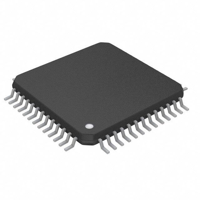
| 描述 | IC INTERFAC PCM COMBO II 28-PLCC接口—CODEC COMBO II Programmable PCM CODEC/Filter 28-PLCC |
| 产品分类 | |
| 品牌 | Texas Instruments |
| 产品手册 | |
| 产品图片 |
|
| rohs | 符合RoHS无铅 / 符合限制有害物质指令(RoHS)规范要求 |
| 产品系列 | 接口 IC,接口—CODEC,Texas Instruments TP3070V-G/NOPBCOMBO®II |
| 数据手册 | |
| 产品型号 | TP3070V-G/NOPB |
| PCN组件/产地 | |
| 三角积分 | 无 |
| 产品目录页面 | |
| 产品种类 | 接口—CODEC |
| 供应商器件封装 | 28-PLCC(11.51x11.51) |
| 信噪比,ADC/DAC(db)(典型值) | - |
| 其它名称 | *TP3070V-G/NOPB |
| 分辨率(位) | - |
| 动态范围,ADC/DAC(db)(典型值) | - |
| 包装 | 管件 |
| 商标 | Texas Instruments |
| 安装类型 | 表面贴装 |
| 安装风格 | SMD/SMT |
| 封装 | Tube |
| 封装/外壳 | 28-LCC(J 形引线) |
| 封装/箱体 | PLCC-28 |
| 工作温度 | 0°C ~ 70°C |
| 工厂包装数量 | 35 |
| 接口类型 | Serial |
| 数据接口 | PCM 音频接口 |
| 最大工作温度 | + 70 C |
| 最小工作温度 | 0 C |
| 标准包装 | 35 |
| 电压-电源,数字 | ±5V |
| 电压-电源,模拟 | ±5V |
| 类型 | PCM |
| 系列 | TP3070 |


- 商务部:美国ITC正式对集成电路等产品启动337调查
- 曝三星4nm工艺存在良率问题 高通将骁龙8 Gen1或转产台积电
- 太阳诱电将投资9.5亿元在常州建新厂生产MLCC 预计2023年完工
- 英特尔发布欧洲新工厂建设计划 深化IDM 2.0 战略
- 台积电先进制程称霸业界 有大客户加持明年业绩稳了
- 达到5530亿美元!SIA预计今年全球半导体销售额将创下新高
- 英特尔拟将自动驾驶子公司Mobileye上市 估值或超500亿美元
- 三星加码芯片和SET,合并消费电子和移动部门,撤换高东真等 CEO
- 三星电子宣布重大人事变动 还合并消费电子和移动部门
- 海关总署:前11个月进口集成电路产品价值2.52万亿元 增长14.8%


PDF Datasheet 数据手册内容提取
TP3070,TP3070-X,TP3071 TP3070, TP3071, TP3070-X COMBO II Programmable PCM CODEC/Filter Literature Number: SNOSBX9
T April1994 P 3 0 7 0 , TP3070, TP3071, TP3070-X T P COMBO® II Programmable PCM CODEC/Filter 3 0 7 General Description Features 1 , TheTP3070andTP3071aresecond-generationcombined n CompleteCODECandFILTERsystemincluding: T PCMCODECandFilterdevicesoptimizedfordigitalswitch- —TransmitandreceivePCMchannelfilters P ing applications on subscriber line and trunk cards. Using —µ-laworA-lawcompandingencoderanddecoder 3 advanced switched capacitor techniques, COMBO II com- —Receivepoweramplifierdrives300W 07 binestransmitbandpassandreceivelowpasschannelfilters —4.096MHzserialPCMdata(max) 0 withacompandingPCMencoderanddecoder.Thedevices n ProgrammableFunctions: -X areA-lawandµ-lawselectableandemployaconventional —Transmitgain:25.4dBrange,0.1dBsteps serial PCM interface capable of being clocked up to —Receivegain:25.4dBrange,0.1dBsteps C 4.096 MHz.Anumber of programmable functions may be —Hybridbalancecancellationfilter O controlledviaaserialcontrolport. —Time-slotassignment;upto64slots/frame M Channelgainsareprogrammableovera25.4dBrangein —2portassignment(TP3070) B eachdirection,andaprogrammablefilterisincludedtoen- —6interfacelatches(TP3070) O ableHybridBalancingtobeadjustedtosuitawiderangeof —Aorµ-law loop impedance conditions. Both transformer and active —Analogloopback II SLICinterfacecircuitswithrealorcomplexterminationim- —Digitalloopback P pedancescanbebalancedbythisfilter,withcancellationin n Directinterfacetosolid-stateSLICs r o excessof30dBbeingreadilyachievablewhenmeasured n SimplifiestransformerSLIC;singlewindingsecondary g acrossthepassbandagainststandardtestterminationnet- n Standardserialcontrolinterface r works. n 80mWoperatingpower(typ) a m ToenableCOMBOIItointerfacetotheSLICcontrolleads,a n 1.5mWstandbypower(typ) numberofprogrammablelatchesareincluded;eachmaybe n DesignedforCCITTandLSSGRapplications m configuredaseitheraninputoranoutput.TheTP3070pro- n TTLandCMOScompatibledigitalinterfaces a vides6latchesandtheTP30715latches. b n Extendedtemperatureversionsavailablefor−40˚Cto l +85˚C(TP3070V-X) e Note:SeealsoAN-614,COMBOIIapplicationguide. P C M C O D E C / F i l t e r COMBO®andTRI-STATE®areregisteredtrademarksofNationalSemiconductorCorporation. ©1999NationalSemiconductorCorporation DS008635 www.national.com
Block Diagram DS008635-1 FIGURE1. Connection Diagrams DS008635-2 OrderNumberTP3071J SeeNSPackageNumberJ20A DS008635-4 OrderNumberTP3071N OrderNumberTP3070V SeeNSPackageNumberN20A (0˚Cto+70˚C) OrderNumberTP3070V-X Pin Descriptions (−40˚Cto+85˚C) SeeNSPackageNumberV28A Pin Description V +5V±5%powersupply. CC V −5V±5%powersupply. BB GND Ground.Allanaloganddigitalsignalsare referencedtothispin. FS TransmitFrameSyncinput.Normallyapulse X orsquarewavewithan8kHzrepetitionrateis appliedtothisinputtodefinethestartofthe transmittimeslotassignedtothisdevice (non-delayeddatatimingmode),orthestartof thetransmitframe(delayeddatatimingmode usingtheinternaltime-slotassignment counter). www.national.com 2
Pin Descriptions (Continued) Pin Description CI/O ThisistheControlDataI/Opinwhichis Pin Description providedontheTP3071.Serialcontrol FSR ReceiveFrameSyncinput.Normallyapulse informationisshiftedtoorreadfromCOMBO orsquarewavewithan8kHzrepetitionrateis IIonthispinwhenCSislow.Thedirectionof appliedtothisinputtodefinethestartofthe thedataisdeterminedbythecurrent receivetimeslotassignedtothisdevice instructionasdefinedinTable1. (non-delayeddatatimingmode),orthestartof CI ThisisaseparateControlInput,availableonly thereceiveframe(delayeddatatimingmode ontheTP3070.ItcanbeconnectedtoCOif usingtheinternaltime-slotassignment required. counter). CO ThisisaseparateControlOutput,available BCLK BitclockinputusedtoshiftPCMdataintoand onlyontheTP3070.ItcanbeconnectedtoCI outoftheD andD pins.BCLKmayvary R X ifrequired. from64kHzto4.096MHzin8kHz CS ChipSelectinput.Whenthispinislow,control increments,andmustbesynchronouswith informationcanbewrittentoorreadfrom MCLK. COMBOIIviatheCI/Opin(orCIandCO). MCLK Masterclockinputusedbytheswitched IL5–IL0 IL5throughIL0areavailableontheTP3070. capacitorfiltersandtheencoderanddecoder IL4throughIL0areavailableontheTP3071. sequencinglogic.Mustbe512kHz,1.536 EachInterfaceLatchI/Opinmaybe MHz,1.544MHz,2.048MHzor4.096MHz individuallyprogrammedasaninputoran andsynchronouswithBCLK. outputdeterminedbythestateofthe VF I TheTransmitanaloghigh-impedanceinput. X correspondingbitintheLatchDirection Voicefrequencysignalspresentonthisinput Register(LDR).Forpinsconfiguredasinputs, areencodedasanA-laworµ-lawPCMbit thelogicstatesensedoneachinputislatched streamandshiftedoutontheselectedD pin. X intotheInterfaceLatchRegister(ILR) VFRO TheReceiveanalogpoweramplifieroutput, whenevercontroldataiswrittentoCOMBOII, capableofdrivingloadimpedancesaslowas whileCSislow,andtheinformationisshifted 300W (dependingonthepeakoverloadlevel outontheCO(orCI/O)pin.Whenconfigured required).PCMdatareceivedontheassigned asoutputs,controldatawrittenintotheILR DRpinisdecodedandappearsatthisoutput appearsatthecorrespondingILpins. asvoicefrequencysignals. MR Thislogicinputmustbepulledlowfornormal DX0 DX1isavailableontheTP3070only;DX0is operationofCOMBOII.Whenpulled DX1 availableonalldevices.TheseTransmitData momentarilyhigh(atleast1µsec.),all TRI-STATE®outputsremaininthehigh programmableregistersinthedevicearereset impedancestateexceptduringtheassigned tothestatesspecifiedunder“Power-On transmittimeslotontheassignedport,during Initialization”. whichthetransmitPCMdatabyteisshifted NC NoConnection.Donotconnecttothispin.Do outontherisingedgesofBCLK. notroutetracesthroughthispin. TS 0 TS 1isavailableontheTP3070only;TS 0is X X X TS 1 availableonalldevices.Normallythese Functional Description X open-drainoutputsarefloatinginahigh impedancestateexceptwhenatime-slotis POWER-ONINITIALIZATION activeononeoftheDXoutputs,whenthe Whenpowerisfirstapplied,power-onresetcircuitryinitial- appropriateTSXoutputpullslowtoenablea izestheCOMBOIIandputsitintothepower-downstate. backplaneline-driver. Thegaincontrolregistersforthetransmitandreceivegain D 0 D 1isavailableontheTP3070only;D 0is sections are programmed to OFF (00000000), the hybrid R R R D 1 availableonalldevices.Thesereceivedata balancecircuitisturnedoff,thepowerampisdisabledand R thedeviceisinthenon-delayedtimingmode.TheLatchDi- inputsareinactiveexceptduringtheassigned rectionRegister(LDR)ispre-setwithallILpinsprogrammed receivetimeslotoftheassignedportwhen asinputs,placingtheSLICinterfacepinsinahighimped- thereceivePCMdataisshiftedinonthe ancestate.TheCI/Opinissetasaninputreadyforthefirst fallingedgesofBCLK. controlbyteoftheinitializationsequence.Otherinitialstates CCLK ControlClockinput.Thisclockshiftsserial intheControlRegisterareindicatedinSection2.0. controlinformationintooroutfromCI/OorCI Aresettothesesameinitialconditionsmayalsobeforcedby andCOwhentheCSinputislow,depending drivingtheMRpinmomentarilyhigh.Thismaybedoneei- onthecurrentinstruction.CCLKmaybe therwhenpowered-upordown.Fornormaloperationthis asynchronouswiththeothersystemclocks. pinmustbepulledlow.Ifnotused,MRshouldbehard-wired toground. Thedesiredmodesforallprogrammablefunctionsmaybe initializedviathecontrolportpriortoaPower-upcommand. 3 www.national.com
Functional Description (Continued) Adecode cycle begins immediately after the assigned re- ceivetime-slot,and10µslatertheDecoderDACoutputis POWER-DOWNSTATE updated.Thetotalsignaldelayis10µsplus120µs(filterde- Following a period of activity in the powered-up state the lay)plus62.5µs(1⁄2frame)whichgivesapproximately190 power-downstatemaybere-enteredbywritinganyofthe µs. controlinstructionsintotheserialcontrolportwiththe“P”bit setto“1”asindicatedinTable1.Itisrecommendedthatthe PCMINTERFACE chipbepowereddownbeforewritinganyadditionalinstruc- TheFS andFS framesyncinputsdeterminethebegin- X R tions.Inthepower-downstate,allnon-essentialcircuitryis ningofthe8-bittransmitandreceivetime-slotsrespectively. de-activatedandtheD 0(andD 1)outputsareinthehigh TheymayhaveanydurationfromasinglecycleofBCLK X X impedanceTRI-STATEcondition. HIGHtooneMCLKperiodLOW.Twodifferentrelationships ThecoefficientsstoredintheHybridBalancecircuitandthe maybeestablishedbetweentheframesyncinputsandthe GainControlregisters,thedataintheLDRandILR,andall actualtime-slotsonthePCMbussesbysettingbit3inthe controlbitsremainunchangedinthepower-downstateun- ControlRegister(seeTable2).Non-delayeddatamodeis lesschangedbywritingnewdataviatheserialcontrolport, similartolong-frametimingontheTP3050/60seriesofde- whichremainsactive.TheoutputsoftheInterfaceLatches vices(COMBO);time-slotsbeginnominallycoincidentwith also remain active, maintaining the ability to monitor and therisingedgeoftheappropriateFSinput.Thealternativeis controltheSLIC. touseDelayedDatamode,whichissimilartoshort-frame synctimingonCOMBO,inwhicheachFSinputmustbehigh TRANSMITFILTERANDENCODER atleastahalf-cycleofBCLKearlierthanthetime-slot.The Time-SlotAssignmentcircuitonthedevicecanonlybeused TheTransmitsectioninput,VF I,isahighimpedancesum- X withDelayedDatatiming. minginputwhichisusedasthedifferencingpointforthein- ternalhybridbalancecancellationsignal.Noexternalcom- WhenusingTime-SlotAssignment,thebeginningofthefirst ponentsarenecessarytosetthegain.Followingthiscircuit time-slotinaframeisidentifiedbytheappropriateFSinput. isaprogrammablegain/attenuationamplifierwhichiscon- The actual transmit and receive time-slots are then deter- trolledbythecontentsoftheTransmitGainRegister(see minedbytheinternalTime-SlotAssignmentcounters. ProgrammableFunctionssection).Anactivepre-filterthen TransmitandReceiveframesandtime-slotsmaybeskewed precedes the 3rd order high-pass and 5th order low-pass fromeachotherbyanynumberofBCLKcycles.Duringeach switched capacitor filters. The A/D converter has a com- assignedTransmittime-slot,theselectedD 0/1outputshifts X pressingcharacteristicaccordingtothestandardCCITTAor dataoutfromthePCMregisterontherisingedgesofBCLK. µ255codinglaws,whichmustbeselectedbyacontrolin- TSX0(orTSX1asappropriate)alsopullslowforthefirst71⁄2 structionduringinitialization(seeTable1andTable2).Apre- bittimesofthetime-slottocontroltheTRI-STATEEnableof cisionon-chipvoltagereferenceensuresaccurateandhighly abackplaneline-driver.SerialPCMdataisshiftedintothe stabletransmissionlevels.Anyoffsetvoltagearisinginthe selectedD 0/1inputduringeachassignedReceivetime-slot R gain-setamplifier,thefiltersorthecomparatoriscanceledby onthefallingedgesofBCLK.D 0orD 1andD 0orD 1 X X R R aninternalauto-zerocircuit. areselectableontheTP3070only,seeSection6. Each encode cycle begins immediately following the as- signedTransmittime-slot.Thetotalsignaldelayreferenced tothestartofthetime-slotisapproximately165µs(dueto the Transmit Filter) plus 125 µs (due to encoding delay), whichtotals290µs.DataisshiftedoutonD 0orD 1during X X theselectedtimeslotoneightrisingedgesofBCLK. DECODERANDRECEIVEFILTER PCMdataisshiftedintotheDecoder’sReceivePCMRegis- terviatheD 0orD 1pinduringtheselectedtime-sloton R R the8fallingedgesofBCLK.TheDecoderconsistsofanex- pandingDACwitheitherAorµ255lawdecodingcharacter- istic,whichisselectedbythesamecontrolinstructionused toselecttheEncodelawduringinitialization.Followingthe Decoderisa5thorderlow-passswitchedcapacitorfilterwith integralSinx/xcorrectionforthe8kHzsampleandhold.A programmablegainamplifier,whichmustbesetbywritingto theReceiveGainRegister,isincluded,andfinallyaPower Amplifiercapableofdrivinga300W loadto±3.5V,a600W loadto±3.8Vora15kW loadto±4.0Vatpeakoverload. www.national.com 4
Functional Description (Continued) TABLE1.ProgrammableRegisterInstructions Function Byte1(Note1) Byte2(Note1) 7 6 5 4 3 2 1 0 7 6 5 4 3 2 1 0 SingleBytePower-Up/Down P X X X X X 0 X None WriteControlRegister P 0 0 0 0 0 1 X SeeTable2 Read-BackControlRegister P 0 0 0 0 1 1 X SeeTable2 WritetoInterfaceLatchRegister P 0 0 0 1 0 1 X SeeTable4 ReadInterfaceLatchRegister P 0 0 0 1 1 1 X SeeTable4 WriteLatchDirectionRegister P 0 0 1 0 0 1 X SeeTable3 ReadLatchDirectionRegister P 0 0 1 0 1 1 X SeeTable3 WriteReceiveGainRegister P 0 1 0 0 0 1 X SeeTable8 ReadReceiveGainRegister P 0 1 0 0 1 1 X SeeTable8 WriteTransmitGainRegister P 0 1 0 1 0 1 X SeeTable7 ReadTransmitGainRegister P 0 1 0 1 1 1 X SeeTable7 WriteReceiveTime-Slot/Port P 1 0 0 1 0 1 X SeeTable6 Read-BackReceiveTime-Slot/Port P 1 0 0 1 1 1 X SeeTable6 WriteTransmitTime-Slot/Port P 1 0 1 0 0 1 X SeeTable6 Read-BackTransmitTime-Slot/Port P 1 0 1 0 1 1 X SeeTable6 WriteHybridBalanceRegister1 P 0 1 1 0 0 1 X ReadHybridBalanceRegister1 P 0 1 1 0 1 1 X Derivefrom Optimization WriteHybridBalanceRegister2 P 0 1 1 1 0 1 X Routinein ReadHybridBalanceRegister2 P 0 1 1 1 1 1 X TP3077SW WriteHybridBalanceRegister3 P 1 0 0 0 0 1 X Program ReadHybridBalanceRegister3 P 1 0 0 0 1 1 X Note1: Bit7ofbytes1and2isalwaysthefirstbitclockedintooroutfromtheCI,COorCI/Opin.X=don’tcare. Note2: “P”isthepower-up/downcontrolbit,see“Power-Up/DownControl”section.(“0”=PowerUp,“1”=PowerDown) Note3: Otherregisteraddresscodesareinvalidandshouldnotbeused. SERIALCONTROLPORT strobedinwhileCSislow,asdefinedinTable1.CSmustbe Control information and data are written into or read-back keptlow,orbetakenlowagainforafurther8CCLKcycles, fromCOMBOIIviatheserialcontrolportconsistingofthe duringwhichthedataisshiftedontotheCOorCI/Opinon control clock CCLK, the serial data input/output CI/O, (or therisingedgesofCCLK.WhenCSishightheCOorCI/O separateinput,CI,andoutput,CO,ontheTP3070only),and pinisinthehigh-impedanceTRI-STATE,enablingtheCI/O theChipSelectinput,CS.Allcontrolinstructionsrequire2 pinsofmanydevicestobemultiplexedtogether. bytes,aslistedinTable1,withtheexceptionofasinglebyte IfCSreturnshighduringeitherbyte1orbyte2beforeall power-up/downcommand.Thebyte1bitsareusedasfol- eightCCLKpulsesofthatbyteoccur,boththebitcountand lows:bit7specifiespoweruporpowerdown;bits6,5,4and bytecountareresetandregistercontentsarenotaffected. 3specifytheregisteraddress;bit2specifieswhetherthein- Thispreventslossofsynchronizationinthecontrolinterface structionisreadorwrite;bit1specifiesaoneortwobytein- aswellascorruptionofregisterdataduetoprocessorinter- struction;andbit0isnotused. ruptorotherproblem.WhenCSreturnslowagain,thede- ToshiftcontroldataintoCOMBOII,CCLKmustbepulsed8 vicewillbereadytoacceptbit1ofbyte1ofanewinstruc- times while CS is low. Data on the CI/O (or CI) input is tion. shifted into the serial input register on the falling edge of eachCCLKpulse.Afteralldataisshiftedin,thecontentsof Programmable Functions theinputshiftregisteraredecoded,andmayindicatethata 2ndbyteofcontroldatawillfollow.Thissecondbytemayei- 1.0POWER-UP/DOWNCONTROL therbedefinedbyasecondbyte-wideCSpulseormayfol- Followingpower-oninitialization,power-upandpower-down lowthefirstcontiguously,i.e.itisnotmandatoryforCStore- controlmaybeaccomplishedbywritinganyofthecontrolin- turnhighbetweenthefirstandsecondcontrolbytes.Atthe structionslistedinTable1intoCOMBOIIwiththe“P”bitset endofCCLK8inthe2ndcontrolbytethedataisloadedinto to“0”forpower-upor“1”forpower-down.Normallyitisrec- theappropriateprogrammableregister.CSmayremainlow ommendedthatallprogrammablefunctionsbeinitiallypro- continuouslywhenprogrammingsuccessiveregisters,ifde- grammed while the device is powered down. Power state sired.However,CSshouldbesethighwhennodatatrans- controlcanthenbeincludedwiththelastprogrammingin- fersareinprogress. structionortheseparatesingle-byteinstruction.Anyofthe ToreadbackInterfaceLatchdataorstatusinformationfrom programmableregistersmayalsobemodifiedwhilethede- COMBO II, the first byte of the appropriate instruction is 5 www.national.com
Programmable Functions (Continued) gainsremainunchanged,thuscaremustbetakentoensure thatoverloadlevelsarenotexceededanywhereintheloop. vice is powered-up or down by setting the “P” bit as indi- Hybridbalancemustbedisabledformeaningfulanalogloop- cated.Whenthepower-upordowncontrolisenteredasa backfunction. singlebyteinstruction,bitone(1)mustberesettoa0. Whenapower-upcommandisgiven,allde-activatedcircuits 2.4DigitalLoopback areactivated,buttheTRI-STATEPCMoutput(s),D 0(and Digital Loopback mode is entered by setting the “AL” and X D 1),willremaininthehighimpedancestateuntilthesec- “DL”bitsintheControlRegisterasshowninTable2.This X ondFS pulseafterpower-up. modeprovidesanotherstageofpathverificationbyenabling X datawrittenintotheReceivePCMRegistertobereadback 2.0CONTROLREGISTERINSTRUCTION fromthatregisterinanyTransmittime-slotatD 0/1.Indigital X ThefirstbyteofaREADorWRITEinstructiontotheControl loopback, the decoder will remain functional and output a RegisterisasshowninTable1.Thesecondbytehasthefol- signalatVFRO.Ifthisisundesirable,thereceiveoutputcan lowingbitfunctions: beturnedoffbyprogrammingthereceivegainregistertoall zeros. TABLE2.ControlRegisterByte2Functions 3.0INTERFACELATCHDIRECTIONS BitNumberandName Immediately following power-on, all Interface Latches as- 7 6 5 4 3 2 1 0 Function sumetheyareinputs,andthereforeallILpinsareinahigh F1 F0 MA IA DN DL AL PP impedance state. Each IL pin may be individually pro- 0 0 MCLK=512kHz grammedasalogicinputoroutputbywritingtheappropriate 0 1 MCLK=1.536 instructiontotheLDR,seeTable1andTable3.Formini- or1.544MHz mumpowerdissipation,unconnectedlatchpinsshouldbe 1 0 MCLK=2.048MHz programmedasoutputs.FortheTP3071,L5shouldalways (Note4) beprogrammedasanoutput. 1 1 MCLK=4.096MHz BitsL –L mustbesetbywritingthespecifiedinstructionto 0 X Selectµ-255law(Note4) theLD5Rw0iththeLbitsinthesecondbytesetasfollows: 1 0 A-law,IncludingEven BitInversion TABLE3.Byte2FunctionsofLatchDirectionRegister 1 1 A-law,NoEvenBitInversion 0 DelayedDataTiming Byte2BitNumber 1 Non-DelayedData 7 6 5 4 3 2 1 0 Timing(Note4) 0 0 NormalOperation L0 L1 L2 L3 L4 L5 X X (Note4) 1 X DigitalLoopback L Bit ILDirection 0 1 AnalogLoopback n 0 Input 0 PowerAmpEnabledinPDN 1 PowerAmpDisabledin 1 Output PDN(Note4) X=don’tcare Note4: Stateatpower-oninitialization.(Bit4=0) INTERFACELATCHSTATES 2.1MasterClockFrequencySelection Interface Latches configured as outputs assume the state AMasterclockmustbeprovidedtoCOMBOIIforoperation determinedbytheappropriatedatabitinthe2-byteinstruc- ofthefilterandcoding/decodingfunctions.TheMCLKfre- tionwrittentotheInterfaceLatchRegister(ILR)asshownin quency must be either 512 kHz, 1.536 MHz, 1.544 MHz, Table1andTable4.Latchesconfiguredasinputswillsense 2.048 MHz, or 4.096 MHz and must be synchronous with the state applied by an external source, such as the BCLK.BitsF andF (seeTable2)mustbesetduringinitial- 1 0 Off-Hook detect output of a SLIC.All bits of the ILR, i.e. izationtoselectthecorrectinternaldivider. sensedinputsandtheprogrammedstateofoutputs,canbe readbackinthe2ndbyteofaREADfromtheILR. 2.2CodingLawSelection Itisrecommendedthatduringinitialization,thestateofIL Bits“MA”and“IA”inTable2permittheselectionofµ255 pinstobeconfiguredasoutputsshouldbeprogrammedfirst, codingorA-lawcoding,withorwithoutevenbitinversion. followedimmediatelybytheLatchDirectionRegister. 2.3AnalogLoopback AnalogLoopbackmodeisenteredbysettingthe“AL”and TABLE4.InterfaceLatchDataBitOrder “DL”bitsintheControlRegisterasshowninTable2.Inthe BitNumber analogloopbackmode,theTransmitinputVF Iisisolated fromtheinputpinandinternallyconnectedtothXeVF Oout- 7 6 5 4 3 2 1 0 R put,formingaloopfromtheReceivePCMRegisterbackto D D D D D D X X 0 1 2 3 4 5 theTransmitPCMRegister.TheVF Opinremainsactive, R andtheprogrammedsettingsoftheTransmitandReceive www.national.com 6
Programmable Functions (Continued) TABLE5.CodingLawConventions TrueA-lawwith A-lawwithout µ255law evenbitinversion evenbitinversion MSB LSB MSB LSB MSB LSB V =+FullScale 10000000 10101010 11111111 IN V =0V 11111111 11010101 10000000 IN 01111111 01010101 00000000 V =−FullScale 00000000 00101010 01111111 IN Note5: TheMSBisalwaysthefirstPCMbitshiftedinoroutofCOMBOII. TABLE6.Time-SlotandPortAssignmentInstruction BitNumberandName Function 7 6 5 4 3 2 1 0 EN PS T T T T T T 5 4 3 2 1 0 (Note6) (Note7) 0 0 X X X X X X DisableD 0Output(TransmitInstruction) X DisableD 0Input(ReceiveInstruction) R 0 1 X X X X X X DisableD 1Output(TransmitInstruction) X DisableD 1Input(ReceiveInstruction) R 1 0 AssignOneBinaryCodedTime-Slotfrom0–63 EnableD 0Output(TransmitInstruction) X AssignOneBinaryCodedTime-Slotfrom0–63 EnableD 0Input(ReceiveInstruction) R 1 1 AssignOneBinaryCodedTime-Slotfrom0–63 EnableD 1Output(TransmitInstruction) X AssignOneBinaryCodedTime-Slotfrom0–63 EnableD 1Input(ReceiveInstruction) R Note6: The“PS”bitMUSTalwaysbesetto0fortheTP3071. Note7: T5istheMSBoftheTime-slotassignmentbitfield.Timeslotbitsshouldbesetto“000000”forbothtransmitandreceivewhenoperatinginnon-delayed datatimingmode. 5.0TIME-SLOTASSIGNMENT Time-SlotAssignmentmoderequiresthattheFS andFS X R COMBOIIcanoperateineitherfixedtime-slotortime-slot pulses must conform to the delayed data timing format assignment mode for selecting the Transmit and Receive showninFigure5. PCMtime-slots.Followingpower-on,thedeviceisautomati- callyinNon-DelayedTimingmode,inwhichthetime-slotal- 6.0PORTSELECTION waysbeginswiththeleading(rising)edgeofframesyncin- OntheTP3070only,anadditionalcapabilityisavailable;2 putsFSXandFSR.Time-SlotAssignmentmayonlybeused TransmitserialPCMports,DX0andDX1,and2Receivese- withDelayedDatatiming;seeFigure5.FSXandFSRmay rial PCM ports, DR0 and DR1, are provided to enable haveanyphaserelationshipwitheachotherinBCLKperiod two-wayspaceswitchingtobeimplemented.Portselections increments. for transmit and receive are made within the appropriate Alternatively,theinternaltime-slotassignmentcountersand time-slotassignmentinstructionusingthe“PS”bitinthesec- comparatorscanbeusedtoaccessanytime-slotinaframe, ondbyte.ThePSbitselectseitherPort0orPort1.Both usingtheframesyncinputsasmarkerpulsesforthebegin- portscannotbeactiveatthesametime. ning of transmit and receive time-slot 0. In this mode, a OntheTP3071,onlyportsDX0andDR0areavailable,there- framemayconsistofupto64time-slotsof8bitseach.A forethe“PS”bitMUSTalwaysbesetto0forthesedevices. time-slot is assigned by a 2-byte instruction as shown in Table6showstheformatforthesecondbyteofbothtrans- Table1andTable6.Thelast6bitsofthesecondbyteindi- mitandreceivetime-slotandportassignmentinstructions. catetheselectedtime-slotfrom0–63usingstraightbinary notation.Whenwritingatimeslotandportassignmentregis- 7.0TRANSMITGAININSTRUCTIONBYTE2 ter,ifthePCMinterfaceiscurrentlyactive,itisimmediately Thetransmitgaincanbeprogrammedin0.1dBstepsby deactivatedtopreventpossiblebusclashes.Anewassign- writingtotheTransmitGainRegisterasdefinedinTable1 mentbecomesactiveonthesecondframefollowingtheend andTable7.Thiscorrespondstoarangeof0dBm0levelsat oftheChip-Selectforthesecondcontrolbyte.Rewritingof VF I between 1.619 Vrms and 0.087 Vrms (equivalent to registercontentsshouldnotbeperformedduringthetalking +6.X4dBmto−19.0dBmin600W ). period of a connection to prevent waveform distortion Tocalculatethebinarycodeforbyte2ofthisinstructionfor causedbylossofasamplewhichwilloccurwitheachregis- anydesiredinput0dBm0levelinVrms,takethenearestin- terwrite.The“EN”bitallowsthePCMinputs,D 0/1,orout- R tegertothedecimalnumbergivenby: puts,D 0/1,asappropriate,tobeenabledordisabled. X 200xlog (V/0.08595) 10 7 www.national.com
Programmable Functions (Continued) ator.Eitherofthefiltersectionscanbebypassedifonlyone isrequiredtoachievegoodcancellation.Aselectable180 and convert to the binary equivalent. Some examples are degreeinvertingstageisincludedtocompensateforinter- giveninTable7andacompletetabulationisgiveninAppen- facecircuitswhichalsoinvertthetransmitinputrelativeto dixIofAN-614. thereceiveoutputsignal.The2ndordersectionisintended ItshouldbenotedthattheTransmit(idlechannel)Noiseand mainly to balance low frequency signals across a trans- Transmit Signal to Total Distortion are both specified with formerSLIC,andthefirstordersectiontobalancemidrange transmitgainsetto0dB(GainRegistersettoallones).At tohigheraudiofrequencysignals. hightransmitgainstherewillbesomedegradationinnoise Asa2ndordersection,Hybal1hasapairoflowfrequency performance for these parameters. See Application Note zeroesandapairofcomplexconjugatepoles.Whenconfig- AN-614formoreinformationonthissubject. uring Hybal1, matching the phase of the hybrid at low to mid-bandfrequenciesismostcritical.Oncetheechopathis correctlybalancedinphase,themagnitudeofthecancella- TABLE7.Byte2ofTransmitGainInstruction tionsignalcanbecorrectedbytheprogrammableattenua- BitNumber 0dBm0TestLevel(Vrms) tor. 76543210 atVF I The2ndordermodeofHybal1ismostsuitableforbalancing X interfaceswithtransformershavinghighinductanceof1.5 00000000 NoOutput(Note8) Henries or more. An alternative configuration for smaller 00000001 0.087 transformersisavailablebyconvertingHybal1toasimple 00000010 0.088 first-ordersectionwithasinglereallow-frequencypoleand — — zero. In this mode, the pole/zero frequency may be pro- grammed. 11111110 1.600 Manylineinterfacescanbeadequatelybalancedbyuseof 11111111 1.619 the Hybal1 section only, in which case the Hybal2 filter shouldbede-selectedtobypassit. cNoodtees8r:epArneasleongtisniggnidallepnaothiseis.cutoff,butDXremainsactiveandwilloutput Hybal2,thehigherfrequencyfirst-ordersection,isprovided forbalancinganelectronicSLIC,andisalsohelpfulwitha 8.0RECEIVEGAININSTRUCTIONBYTE2 transformerSLICinprovidingadditionalphasecorrectionfor midandhigh-bandfrequencies,typically1kHzto3.4kHz. Thereceivegaincanbeprogrammedin0.1dBstepsbywrit- Suchacorrectionisparticularlyusefulifthetestbalanceim- ingtotheReceiveGainRegisterasdefinedinTable1and pedanceincludesacapacitorof100nForless,suchasthe Table8.Notethefollowingrestrictionsonoutputdrivecapa- loaded and non-loaded loop test networks in the United bility: States.Independentplacementofthepoleandzerolocation a) 0dBm0levels£ 1.96VrmsatVF Omaybedriveninto R isprovided. aloadof‡ 15kW toGND;receivegainsetto0dB(Gain Registersettoallones) Figure2showsasimplifieddiagramofthelocalechopath for a typical application with a transformer interface. The b) 0dBm0levels£ 1.85VrmsatVF Omaybedriveninto R magnitudeandphaseofthelocalechosignal,measuredat aloadof‡ 600W toGND;receivegainsetto−0.5dB VF I,areafunctionoftheterminationimpedanceZ ,theline c) 0adloBamd0ofle‡ve3l0s0£W 1t.o71GVNrDm;sreacteVivFeROgaminasyebtetod−ri1v.e2ndiBnto tpreadnXasfnocremererfalencdtetdhebiamcpkeidnatonctheeoftrtahnes2foWrmloeorpp,rZimL.aTIrfythiseeimx-- Tocalculatethebinarycodeforbyte2ofthisinstructionfor pressed as Z ' then the echo path transfer function from L anydesiredoutput0dBm0levelinVrms,takethenearestin- VF OtoVF Iis: R X tegertothedecimalnumbergivenby: H(w)=Z '/(Z +Z ') (1) L T L 200xlog (V/0.1043) 10 and convert to the binary equivalent. Some examples are 9.1PROGRAMMINGTHEFILTER giveninTable8andacompletetabulationisgiveninAppen- Oninitialpower-up,theHybridBalancefilterisdisabled.Be- dixIofAN-614. forethehybridbalancefiltercanbeprogrammeditisneces- sarytodesignthetransformerandterminationimpedancein order to meet system 2W input return loss specifications, TABLE8.Byte2ofReceiveGainInstruction whicharenormallymeasuredagainstafixedtestimpedance BitNumber 0dBm0TestLevel(Vrms) (600 or 900W in most countries). Only then can the echo pathbemodeledandthehybridbalancefilterprogrammed. 76543210 atVF O R Hybridbalancingisalsomeasuredagainstafixedtestim- 00000000 NoOutput(LowZtoGND) pedance,specifiedbyeachnationalTelecomadministration 00000001 0.105 toprovideadequatecontroloftalkerandlistenerechoover themajorityoftheirnetworkconnections.Thistestimped- 00000010 0.107 anceisZ inFigure2.Theechosignalandthedegreeof — — transhybriLdlossobtainedbytheprogrammablefiltermustbe 11111110 1.941 measuredfromthePCMdigitalinput,D 0,tothePCMdigi- R 11111111 1.964 tal output, DX0, either by digital test signal analysis or by conversionbacktoanalogbyaPCMCODEC/Filter. 9.0HYBRIDBALANCEFILTER TheHybridBalanceFilteronCOMBOIIisaprogrammable filterconsistingofasecond-ordersection,Hybal1,followed byafirst-ordersection,Hybal2,andaprogrammableattenu- www.national.com 8
Programmable Functions (Continued) DS008635-5 FIGURE2.SimplifiedDiagramofHybridBalanceCircuit ThreeregistersmustbeprogrammedinCOMBOIItofully POWERSUPPLIES configuretheHybridBalanceFilterasfollows: WhilethepinsoftheTP3070COMBOIIdevicesarewell Register1: select/de-selectHybridBalanceFilter; protectedagainstelectricalmisuse,itisrecommendedthat invert/non-invertcancellationsignal; thestandardCMOSpracticeofapplyingGNDtothedevice before any other connections are made should always be select/de-selectHybal2filtersection; followed.Inapplicationswheretheprintedcircuitcardmay attenuatorsetting. bepluggedintoahotsocketwithpowerandclocksalready Register2: select/de-selectHybal1filter; present,extralongpinsontheconnectorshouldbeusedfor setHybal1to2ndorderor1storder; groundandVBB.Inaddition,aSchottkydiodeshouldbecon- nectedbetweenV andground. poleandzerofrequencyselection. BB Tominimizenoisesources,allgroundconnectionstoeach Register3: programpolefrequencyinHybal2filter; deviceshouldmeetatacommonpointascloseaspossible programzerofrequencyinHybal2filter. tothedeviceGNDpininordertopreventtheinteractionof Standardfilterdesigntechniquesmaybeusedtomodelthe groundreturncurrentsflowingthroughacommonbusim- echopath(seeEquation(1))anddesignamatchinghybrid pedance. Power supply decoupling capacitors of 0.1 µF balance filter configuration.Alternatively, the frequency re- shouldbeconnectedfromthiscommondevicegroundpoint sponseoftheechopathcanbemeasuredandthehybrid toV andV asclosetothedevicepinsaspossible.V CC BB CC balancefilterdesignedtoreplicateit. andV shouldalsobedecoupledwithLowEffectiveSeries BB AHybridBalancefilterdesignguideandsoftwareoptimiza- Resistance Capacitors of at least 10 µF located near the tionprogramareavailableunderlicensefromNationalSemi- cardedgeconnector. conductorCorporation;orderTP3077SW. FurtherguidelinesonPCBlayouttechniquesareprovidedin ApplicationNoteAN-614,“COMBOII™ProgrammablePCM Applications Information CODEC/FilterFamilyApplicationGuide”. Figure3showsatypicalapplicationoftheTP3071together withatypicalmonolithicSLIC.FouroftheILlatchesarecon- figuredasoutputstocontroltherelaydriversontheSLIC, whileIL4isaninputfortheSupervisionsignal. 9 www.national.com
Applications Information (Continued) DS008635-7 FIGURE3.TypicalApplicationwithMonolithicSLIC www.national.com 10
Absolute Maximum Ratings (Note 9) StorageTemperatureRange −65˚Cto+150˚C If Military/Aerospace specified devices are required, VBBtoGND −7V pleasecontacttheNationalSemiconductorSalesOffice/ CurrentatVF 0 ±100mA R Distributorsforavailabilityandspecifications. CurrentatanyDigitalOutput ±50mA V toGND 7V LeadTemperature CC VoltageatVF I V +0.5VtoV −0.5V (Soldering,10sec.) 300˚C X CC BB VoltageatanyDigitalInput V +0.5VtoGND−0.5V CC Electrical Characteristics Unlessotherwisenoted,limitsprintedinBOLDcharactersareguaranteedforV =+5V±5%,V =−5V±5%;T =0˚Cto +70˚C(−40˚Cto+85˚CforTP3070-X)bycorrelationwith100%electricaltestingCCatT =25˚C.AllBoBtherlimitsareaAssuredby A correlationwithotherproductiontestsand/orproductdesignandcharacterization.AllsignalsreferencedtoGND.Typicals specifiedatV =+5V,V =−5V,T =25˚C. CC BB A Symbol Parameter Conditions Min Typ Max Units DIGITALINTERFACES V InputLowVoltage AllDigitalInputs(DCMeas.)(Note10) 0.7 V IL V InputHighVoltage AllDigitalInputs(DCMeas.)(Note10) 2.0 V IH V OutputLowVoltage D 0,D 1,TS 0,TS 1andCO,I =3.2mA, 0.4 V OL X X X X L AllOtherDigitalOutputs,I =1mA L V OutputHighVoltage D 0,D 1andCO,I =−3.2mA, 2.4 V OH X X L AllOtherDigitalOutputs(exceptTS ),I =−1mA X L AllDigitalOutputs,I =−100µA V −0.5 V L CC I InputLowCurrent AnyDigitalInput,GND<V <V −10 10 µA IL IN IL I InputHighCurrent AnyDigitalInputexceptMR,V <V <V −10 10 µA IH IH IN CC MROnly −10 100 µA I OutputCurrentin D 0,D 1,TS 0,TS 1,COandCI/O(asanOutput) OZ X X X X HighImpedance IL5–IL0WhenSelectedasInputs −10 10 µA State(TRI-STATE) GND<V <V OUT CC −40˚Cto+85˚C(TP3070-X) −30 30 µA ANALOGINTERFACES I InputCurrent,VF I −3.3V<VF I<3.3V −10.0 10.0 µA VFXI X X R InputResistance −3.3V<VF I<3.3V 390 620 kW VFXI X VOS InputOffsetVoltage TransmitGain=0dB 200 mV X AppliedatVF I TransmitGain=25.4dB 10 mV X RL LoadResistance ReceiveGain=0dB 15k VFRO ReceiveGain=−0.5dB 600 W ReceiveGain=−1.2dB 300 CL LoadCapacitance RL ‡ 300W 200 pF VFRO VFRO CL fromVF OtoGND VFRO R RO OutputResistance SteadyZeroPCMCodeAppliedto 1.0 3.0 W VFRO D 0orD 1 R R VOS OutputOffset Alternating±ZeroPCMCodeAppliedto −200 200 mV R VoltageatV D 0orD 1,MaximumReceiveGain FRO R R POWERDISSIPATION I 0 PowerDownCurrent CCLK,CI/O,CI,CO,=0.4V,CS=2.4V CC InterfaceLatchesSetasOutputswithNoLoad, 0.1 0.6 mA AllOtherInputsActive,PowerAmpDisabled I 0 PowerDownCurrent AsAbove −0.1 −0.3 mA BB −40˚Cto+85˚C(TP3070-X) −0.4 mA I 1 PowerUpCurrent CCLK,CI/O,CI,CO=0.4V,CS=2.4V CC NoLoadonPowerAmp 8.0 11.0 mA InterfaceLatchesSetasOutputswithNoLoad −40˚Cto+85˚C(TP3070-X) 13.0 mA 11 www.national.com
Electrical Characteristics (Continued) Unlessotherwisenoted,limitsprintedinBOLDcharactersareguaranteedforV =+5V±5%,V =−5V±5%;T =0˚Cto +70˚C(−40˚Cto+85˚CforTP3070-X)bycorrelationwith100%electricaltestingCCatT =25˚C.AllBoBtherlimitsareaAssuredby A correlationwithotherproductiontestsand/orproductdesignandcharacterization.AllsignalsreferencedtoGND.Typicals specifiedatV =+5V,V =−5V,T =25˚C. CC BB A Symbol Parameter Conditions Min Typ Max Units POWERDISSIPATION I 1 PowerUpCurrent AsAbove −8.0 −11.0 mA BB −40˚Cto+85˚C(TP3070-X) −13.0 mA I 2 PowerDownCurrent PowerAmpEnabled 2.0 3.0 mA CC −40˚Cto+85˚C(TP3070-X) 4.0 mA I 2 PowerDownCurrent PowerAmpEnabled −2.0 −3.0 mA BB −40˚Cto+85˚C(TP3070-X) −4.0 mA Note9: “AbsoluteMaximumRatings”indicatelimitsbeyondwhichdamagetothedevicemayoccur.OperatingRatingsindicateconditionsforwhichthedeviceis functional,butdonotguaranteespecificperformancelimits. Note10: Seedefinitionsandtimingconventionssection. Timing Specifications Unlessotherwisenoted,limitsprintedinBOLDcharactersareguaranteedforV =+5V±5%;V =−5V±5%;T =0˚Cto +70˚C(−40˚Cto+85˚CforTP3070-X)bycorrelationwith100%electricaltestingCCatT =25˚C.AllBoBtherlimitsareaAssuredby A correlationwithotherproductiontestsand/orproductdesignandcharacterization.AllsignalsreferencedtoGND.Typicals specifiedatV =+5V,V =−5V,T =25˚C. AlltimingparaCmCetersaremBBeasuredatAV =2.0VandV =0.7V. OH OL SeeDefinitionsandTimingConventionssectionfortestmethodsinformation. Symbol Parameter Conditions Min Typ Max Units MASTERCLOCKTIMING f FrequencyofMCLK SelectionofFrequencyis 512 kHz MCLK Programmable(SeeTable5) 1536 kHz 1544 kHz 2048 kHz 4096 kHz t PeriodofMCLKHigh MeasuredfromV toV (Note11) 80 ns WMH IH IH t PeriodofMCLKLow MeasuredfromV toV (Note11) 80 ns WML IL IL t RiseTimeofMCLK MeasuredfromV toV 30 ns RM IL IH t FallTimeofMCLK MeasuredfromV toV 30 ns FM IH IL t HOLDTime,BCLKLOW TP3070Only 50 ns HBM toMCLKHIGH t PeriodofF orF Low MeasuredfromV toV 1 MCLKPeriod WFL SX SR IL IL PCMINTERFACETIMING f FrequencyofBCLK MayVaryfrom64kHzto4096kHz 64 4096 kHz BCLK in8kHzIncrements t PeriodofBCLKHigh MeasuredfromV toV 80 ns WBH IH IH t PeriodofBCLKLow MeasuredfromV toV 80 ns WBL IL IL t RiseTimeofBCLK MeasuredfromV toV 30 ns RB IL IH t FallTimeofBCLK MeasuredfromV toV 30 ns FB IH IL t HoldTime,BCLKLow 30 ns HBF toFS HighorLow X/R t SetupTime,FS 30 ns SFB X/R HightoBCLKLow t DelayTime,BCLKHigh Load=100pFPlus2LSTTLLoads 80 ns DBD toDataValid −40˚Cto+85˚C(TP3070-X) 90 ns www.national.com 12
Timing Specifications (Continued) Unlessotherwisenoted,limitsprintedinBOLDcharactersareguaranteedforV =+5V±5%;V =−5V±5%;T =0˚Cto +70˚C(−40˚Cto+85˚CforTP3070-X)bycorrelationwith100%electricaltestingCCatT =25˚C.AllBoBtherlimitsareaAssuredby A correlationwithotherproductiontestsand/orproductdesignandcharacterization.AllsignalsreferencedtoGND.Typicals specifiedatV =+5V,V =−5V,T =25˚C. AlltimingparaCmCetersaremBBeasuredatAV =2.0VandV =0.7V. OH OL SeeDefinitionsandTimingConventionssectionfortestmethodsinformation. Symbol Parameter Conditions Min Typ Max Units PCMINTERFACETIMING t DelayTime,BCLKLowtoD 0/1 D 0/1DisabledismeasuredatV DBZ X X OL DisabledifFSXLow,FSXLowto orVOHaccordingtoFigure4or Figure5 D 0/1disabledif8thBCLK 15 80 ns X Low,orBCLKHightoD 0/1 X DisabledifFS High −40˚Cto+85˚C(TP3070-X) 15 100 ns X t DelayTime,BCLKHightoTS Load=100pFPlus2LSTTLLoads 60 ns DBT X LowifFS High,orFS Highto X X TS LowifBCLKHigh(Non X DelayedMode);BCLKHighto TS Low(DelayedDataMode) X t TRI-STATETime,BCLKLowto 15 60 ns ZBT TS HighifFS Low,FS Low X X X toTS Highif8thBCLKLow,or X BCLKHightoTS HighifFS X X High t DelayTime,FS Load=100pFPlus2LSTTLLoads, DFD X/R HightoDataValid AppliesifFS RisesLaterthan 80 ns X/R BCLKRisingEdgeinNon-Delayed DataModeOnly −40˚Cto+85˚C(TP3070-X) 90 ns t SetupTime,D 0/1 30 ns SDB R ValidtoBCLKLow t HoldTime,BCLK 15 ns HBD LowtoD 0/1Invalid −40˚Cto+85˚C(TP3070-X) 15 ns R SERIALCONTROLPORTTIMING f FrequencyofCCLK 2048 kHz CCLK t PeriodofCCLKHigh MeasuredfromV toV 160 ns WCH IH IH t PeriodofCCLKLow MeasuredfromV toV 160 ns WCL IL IL t RiseTimeofCCLK MeasuredfromV toV 50 ns RC IL IH t FallTimeofCCLK MeasuredfromV toV 50 ns FC IH IL t HoldTime,CCLKLow CCLK1 10 ns HCS toCSLow t HoldTime,CCLK CCLK8 100 ns HSC LowtoCSHigh t SetupTime,CS 60 ns SSC TransitiontoCCLKLow t SetupTime,CS 50 ns SSCO TransitiontoCCLKHigh t SetupTime,CI(CI/O) 50 ns SDC DataIntoCCLKLow t HoldTime,CCLK 50 ns HCD LowtoCI/OInvalid t DelayTime,CCLKHigh Load=100pFplus2LSTTLLoads 80 ns DCD toCI/ODataOutValid −40˚Cto+85˚C(TP3070-X) 100 ns 13 www.national.com
Timing Specifications (Continued) Unlessotherwisenoted,limitsprintedinBOLDcharactersareguaranteedforV =+5V±5%;V =−5V±5%;T =0˚Cto +70˚C(−40˚Cto+85˚CforTP3070-X)bycorrelationwith100%electricaltestingCCatT =25˚C.AllBoBtherlimitsareaAssuredby A correlationwithotherproductiontestsand/orproductdesignandcharacterization.AllsignalsreferencedtoGND.Typicals specifiedatV =+5V,V =−5V,T =25˚C. AlltimingparaCmCetersaremBBeasuredatAV =2.0VandV =0.7V. OH OL SeeDefinitionsandTimingConventionssectionfortestmethodsinformation. Symbol Parameter Conditions Min Typ Max Units SERIALCONTROLPORTTIMING t DelayTime,CSLow AppliesOnlyifSeparate 80 ns DSD toCO(CI/O)Valid CSusedforByte2 −40˚Cto+85˚C(TP3070-X) 100 ns t DelayTime,CSor9thCCLK AppliestoEarlierofCSHighor9th DDZ HightoCO(CI/O)High CCLKHigh 15 80 ns Impedance INTERFACELATCHTIMING t SetupTime,ILto InterfaceLatchInputsOnly 100 ns SLC CCLK8ofByte1 t HoldTime,ILValidfrom 50 ns HCL 8thCCLKLow(Byte1) t DelayTimeCCLK8of InterfaceLatchOutputsOnly 200 ns DCL Byte2toIL C =50pF L MASTERRESETPIN t Durationof 1 µs WMR MasterResetHigh Note11: AppliesonlytoMCLKFrequencies‡ 1.536MHz.At512kHza50:50±2%DutyCyclemustbeused. Timing Diagrams DS008635-8 FIGURE4.NonDelayedDataTimingMode www.national.com 14
Timing Diagrams (Continued) DS008635-9 FIGURE5.DelayedDataTimingMode (TimeSlotZeroOnly) 15 www.national.com
Timing Diagrams (Continued) DS008635-10 g n mi Ti ort P ol ntr o C 6. E R U G FI www.national.com 16
Transmission Characteristics Unlessotherwisenoted,limitsprintedinBOLDcharactersareguaranteedforV =+5V±5%,V =−5V±5%;T =0˚Cto +70˚C(−40˚Cto+85˚CforTP3070-X)bycorrelationwith100%electricaltestingCCatT =25˚C.f=BB1015.625Hz,VFAI= 0dBm0,D 0orD 1=0dBm0PCMcode.TransmitandreceivegainsprogrammedAformaximum0dBm0testleveXls(0dB R R gain),hybridbalancefilterdisabled.Allotherlimitsareassuredbycorrelationwithotherproductiontestsand/orproductde- signandcharacterization.AllsignalsreferencedtoGND.TypicalsspecifiedatV =+5V,V =−5V,T =25˚C. CC BB A Symbol Parameter Conditions Min Typ Max Units AMPLITUDERESPONSE AbsoluteLevels TheMaximum0dBm0Levelsare: VF I 1.619 Vrms X VF O(15kW Load) 1.964 Vrms R TheMinimum0dBm0Levelsare: VF I 87.0 mVrms X VF O(AnyLoad‡ 300W ) 105.0 mVrms R OverloadLevelsare3.17dBm0(µLaw) and3.14dBm0(A-Law) G TransmitGain TransmitGainProgrammedforMaximum XA AbsoluteAccuracy 0dBm0TestLevel.(All1’singainregister) MeasureDeviationofDigitalCodefrom Ideal0dBm0PCMCodeatD 0/1. X T =25˚C −0.15 0.15 dB A G TransmitGain T =25˚C,V =5V,V =5V XAG A CC BB Variationwith ProgrammedGainfrom0dBto19dB ProgrammedGain (0dBm0Levelsof1.619Vrmsto 0.182Vrms) −0.1 0.1 dB ProgrammedGainfrom19.1dBto25.4dB (0dBm0Levelsof0.180Vrmsto 0.087Vrms) −0.3 0.3 dB Note:±0.1dBmin/maxisavailableasaselected part. G TransmitGain Relativeto1015.625Hz,(Note15) XAF Variationwith MinimumGain<G <MaximumGain X Frequency f=60Hz −26 dB f=200Hz −1.8 −0.1 dB f=300Hzto3000Hz −0.15 0.15 dB f=3400Hz −0.7 0.0 dB f=4000Hz −14 dB f‡ 4600Hz.MeasureResponse −32 dB atAliasFrequencyfrom0kHzto4kHz. G =0dB,VF I=1.619Vrms X X Relativeto1015.625Hz f=62.5Hz −24.9 dB f=203.125Hz −1.7 −0.1 dB f=343.75Hz −0.15 0.15 dB f=515.625Hz −0.15 0.15 dB f=2140.625Hz −0.15 0.15 dB f=3156.25Hz −0.15 0.15 dB f=3406.250Hz −0.74 0.0 dB f=3984.375Hz −13.5 dB Relativeto1062.5Hz(Note15) f=5250Hz,Measure2750Hz −32 dB f=11750Hz,Measure3750Hz −32 dB f=49750Hz,Measure1750Hz −32 dB 17 www.national.com
Transmission Characteristics (Continued) Unlessotherwisenoted,limitsprintedinBOLDcharactersareguaranteedforV =+5V±5%,V =−5V±5%;T =0˚Cto +70˚C(−40˚Cto+85˚CforTP3070-X)bycorrelationwith100%electricaltestingCCatT =25˚C.f=BB1015.625Hz,VFAI= 0dBm0,D 0orD 1=0dBm0PCMcode.TransmitandreceivegainsprogrammedAformaximum0dBm0testleveXls(0dB R R gain),hybridbalancefilterdisabled.Allotherlimitsareassuredbycorrelationwithotherproductiontestsand/orproductde- signandcharacterization.AllsignalsreferencedtoGND.TypicalsspecifiedatV =+5V,V =−5V,T =25˚C. CC BB A Symbol Parameter Conditions Min Typ Max Units AMPLITUDERESPONSE G TransmitGain MeasuredRelativetoG ,V =5V, XAT XA CC Variationwith V =−5V, −0.1 0.1 dB BB Temperature Minimumgain<G <MaximumGain X −40˚Cto+85˚C(TP3070-X) −0.15 0.15 dB G TransmitGain SinusoidalTestMethod. XAL VariationwithSignal ReferenceLevel=0dBm0. Level VF I=−40dBm0to+3dBm0 −0.2 0.2 dB X VF I=−50dBm0to−40dBm0 −0.4 0.4 dB X VF I=−55dBm0to−50dBm0 −1.2 1.2 dB X G ReceiveGain ReceiveGainProgrammedforMaximum RA AbsoluteAccuracy 0dBm0TestLevel(All1’sin GainRegister).Apply0dBm0PCMCode toD 0orD 1.MeasureVF O. R R R T =25˚C −0.15 0.15 dB A G ReceiveGain T =25˚C,V =5V,V =−5V RAG A CC BB Variationwith ProgrammedGainfrom0dBto19dB ProgrammedGain (0dBm0Levelsof1.964Vrmsto 0.220Vrms) −0.1 0.1 dB ProgrammedGainfrom19.1dBto25.4dB (0dBm0Levelsof0.218Vrmsto 0.105Vrms) −0.3 0.3 dB Note:±0.1dBmin/maxisavailableasaselected part. G ReceiveGain MeasuredRelativetoG . RAT RA VariationwithTemperature V =5V,V =−5V. −0.1 0.1 dB CC BB MinimumGain<G <MaximumGain R −40˚Cto+85˚C(TP3070-X) −0.15 0.15 dB G ReceiveGain Relativeto1015.625Hz,(Note15) RAF VariationwithFrequency D 0orD 1=0dBm0code. R R MinimumGain<G <MaximumGain R f=200Hz −0.25 0.15 dB f=300Hzto3000Hz −0.15 0.15 dB f=3400Hz −0.7 0.0 dB f=4000Hz −14 dB G =0dB,D 0=0dBm0Code, R R G =0dB(Note15) X f=296.875Hz −0.15 0.15 dB f=1875.00Hz −0.15 0.15 dB f=2906.25Hz −0.15 0.15 dB f=2984.375Hz −0.15 0.15 dB f=3406.250Hz −0.74 0.0 dB f=3984.375Hz −13.5 dB www.national.com 18
Transmission Characteristics (Continued) Unlessotherwisenoted,limitsprintedinBOLDcharactersareguaranteedforV =+5V±5%,V =−5V±5%;T =0˚Cto +70˚C(−40˚Cto+85˚CforTP3070-X)bycorrelationwith100%electricaltestingCCatT =25˚C.f=BB1015.625Hz,VFAI= 0dBm0,D 0orD 1=0dBm0PCMcode.TransmitandreceivegainsprogrammedAformaximum0dBm0testleveXls(0dB R R gain),hybridbalancefilterdisabled.Allotherlimitsareassuredbycorrelationwithotherproductiontestsand/orproductde- signandcharacterization.AllsignalsreferencedtoGND.TypicalsspecifiedatV =+5V,V =−5V,T =25˚C. CC BB A Symbol Parameter Conditions Min Typ Max Units AMPLITUDERESPONSE G ReceiveGain SinusoidalTestMethod. RAL VariationwithSignal ReferenceLevel=0dBm0. Level D 0=−40dBm0to+3dBm0 −0.2 0.2 dB R D 0=−50dBm0to−40dBm0 −0.4 0.4 dB R D 0=−55dBm0to−50dBm0 −1.2 1.2 dB R D 0=3.1dBm0 R R =600W ,G =−0.5dB −0.2 0.2 dB L R R =300W ,G =−1.2dB −0.2 0.2 dB L R ENVELOPEDELAYDISTORTIONWITHFREQUENCY D TxDelay,Absolute f=1600Hz 315 µs XA D TxDelay,RelativetoD f=500–600Hz 220 µs XR XA f=600–800Hz 145 µs f=800–1000Hz 75 µs f=1000–1600Hz 40 µs f=1600–2600Hz 75 µs f=2600–2800Hz 105 µs f=2800–3000Hz 155 µs D RxDelay,Absolute f=1600Hz 200 µs RA D RxDelay,RelativetoD f=500–1000Hz −40 µs RR RA f=1000–1600Hz −30 µs f=1600–2600Hz 90 µs f=2600–2800Hz 125 µs f=2800–3000Hz 175 µs NOISE N TransmitNoise,CMessage (Note12) 12 15 dBrnC0 XC Weighted,µ-lawSelected All‘1’sinGainRegister N TransmitNoise,PMessage (Note12) −74 −67 dBm0p XP Weighted,A-lawSelected All‘1’sinGainRegister N ReceiveNoise,CMessage PCMCodeisAlternatingPositive 8 11 dBrnC0 RC Weighted,µ-lawSelected andNegativeZero N ReceiveNoise,PMessage PCMCodeEqualsPositiveZero −82 −79 dBm0p RP Weighted,A-lawSelected N Noise,SingleFrequency f=0kHzto100kHz,LoopAround −53 dBm0 RS Measurement,VF I=0Vrms X PPSR PositivePowerSupply V =5.0V +100mVrms X CC DC Rejection,Transmit f=0kHz–4kHz(Note13) 36 dBC f=4kHz–50kHz 30 dBC NPSR NegativePowerSupply V =−5.0V +100mVrms X BB DC Rejection,Transmit f=0kHz–4kHz(Note13) 36 dBC f=4kHz–50kHz 30 dBC 19 www.national.com
Transmission Characteristics (Continued) Unlessotherwisenoted,limitsprintedinBOLDcharactersareguaranteedforV =+5V±5%,V =−5V±5%;T =0˚Cto +70˚C(−40˚Cto+85˚CforTP3070-X)bycorrelationwith100%electricaltestingCCatT =25˚C.f=BB1015.625Hz,VFAI= 0dBm0,D 0orD 1=0dBm0PCMcode.TransmitandreceivegainsprogrammedAformaximum0dBm0testleveXls(0dB R R gain),hybridbalancefilterdisabled.Allotherlimitsareassuredbycorrelationwithotherproductiontestsand/orproductde- signandcharacterization.AllsignalsreferencedtoGND.TypicalsspecifiedatV =+5V,V =−5V,T =25˚C. CC BB A Symbol Parameter Conditions Min Typ Max Units NOISE PPSR PositivePowerSupply PCMCodeEqualsPositiveZero R Rejection,Receive V =5.0V +100mVrms CC DC MeasureVF O R f=0Hz–4000Hz 36 dBC f=4kHz–25kHz 40 dB f=25kHz–50kHz 36 dB NPSR NegativePowerSupply PCMCodeEqualsPositiveZero R Rejection,Receive V =−5.0V +100mVrms BB DC MeasureVF O R f=0Hz–4000Hz 36 dBC f=4kHz–25kHz 40 dB f=25kHz–50kHz 36 dB SOS SpuriousOut-of-Band 0dBm0,300Hzto3400HzInputPCM SignalsattheChannel CodeAppliedatD 0(orD 1) R R Output 4600Hz–7600Hz −30 dB 7600Hz–8400Hz −40 dB 8400Hz–50,000Hz −30 dB DISTORTION STD SignaltoTotalDistortion SinusoidalTestMethod X STD TransmitorReceive Level=3.0dBm0 33 dBC R Half-Channel,µ-lawSelected =0dBm0to−30dBm0 36 dBC =−40dBm0 30 dBC =−45dBm0 25 dBC STD SignaltoTotalDistortion SinusoidalTestMethod RL Receivewith Level=+3.1dBm0 ResistiveLoad R =600W ,G =−0.5dB 33 dBC L R R =300W ,G =−1.2dB 33 dBC L R SFD SingleFrequency −46 dB X Distortion,Transmit SFD SingleFrequency −46 dB R Distortion,Receive IMD IntermodulationDistortion TransmitorReceive TwoFrequenciesintheRange −41 dB 300Hz–3400Hz www.national.com 20
Transmission Characteristics (Continued) Unlessotherwisenoted,limitsprintedinBOLDcharactersareguaranteedforV =+5V±5%,V =−5V±5%;T =0˚Cto +70˚C(−40˚Cto+85˚CforTP3070-X)bycorrelationwith100%electricaltestingCCatT =25˚C.f=BB1015.625Hz,VFAI= 0dBm0,D 0orD 1=0dBm0PCMcode.TransmitandreceivegainsprogrammedAformaximum0dBm0testleveXls(0dB R R gain),hybridbalancefilterdisabled.Allotherlimitsareassuredbycorrelationwithotherproductiontestsand/orproductde- signandcharacterization.AllsignalsreferencedtoGND.TypicalsspecifiedatV =+5V,V =−5V,T =25˚C. CC BB A Symbol Parameter Conditions Min Typ Max Units CROSSTALK CTX-R TransmittoReceive f=300Hz–3400Hz −90 −75 dB Crosstalk,0dBm0Transmit D =IdleCode Level R CTR-X ReceivetoTransmit f=300Hz–3400Hz −90 −70 dB Crosstalk,0dBm0Receive (Note13) Level Note12: MeasuredbygroundedinputatVFXI. Note13: PPSRX,NPSRX,andCTR–Xaremeasuredwitha−50dBm0activationsignalappliedtoVFXI. Note14: AsignalisValidifitisaboveVIHorbelowVILandInvalidifitisbetweenVILandVIH.Forthepurposesofthisspecificationthefollowingconditionsapply: a)Allinputsignalsaredefinedas:VIL=0.4V,VIH=2.7V,tR<10ns,tF<10ns. b)tRismeasuredfromVILtoVIH.tFismeasuredfromVIHtoVIL. c)DelayTimesaremeasuredfromtheinputsignalValidtotheoutputsignalValid. d)SetupTimesaremeasuredfromthedatainputValidtotheclockinputInvalid. e)HoldTimesaremeasuredfromtheclocksignalValidtothedatainputInvalid. f)PulsewidthsaremeasuredfromVILtoVILorfromVIHtoVIH. Note15: Amulti-tonetesttechniqueisused. 21 www.national.com
Definitions and Timing Conventions DEFINITIONS pulsewidthsaremeasuredfromV to IH VIH VIHistheD.C.inputlevelabovewhich VIH. aninputlevelisguaranteedtoappearas PulseWidthLow The low pulse width is designated as a logical one. This parameter is to be t , where zz represents the mne- WzzL measured by performing a functional monicoftheinputoroutputsignalwhose testatreducedclockspeedsandnomi- pulsewidthisbeingspecified.Lowpulse naltiming,(i.e.,notminimumsetupand widthsaremeasuredfromV toV . IL IL hold times or output strobes), with the SetupTime Setup times are designated as t , highlevelofalldrivingsignalssettoVIH where ww represents the mnemoSnwicwxoxf and maximum supply voltages applied theinputsignalwhosesetuptimeisbe- tothedevice. ingspecifiedrelativetoaclockorstrobe V V istheD.C.inputlevelbelowwhich input represented by mnemonic xx. IL IL aninputlevelisguaranteedtoappearas Setuptimesaremeasuredfromtheww alogicalzerotothedevice.Thisparam- ValidtoxxInvalid. eterismeasuredinthesamemanneras HoldTime Hold times are designated as T , Hwwxx VIHbutwithalldrivingsignallowlevels where ww represents the mnemonic of settoVILandminimumsupplyvoltages theinputsignalwhoseholdtimeisbeing appliedtothedevice. specifiedrelativetoaclockorstrobein- V V istheminimumD.C.outputlevelto put represented by the mnemonic xx. OH OH whichanoutputplacedinalogicalone HoldtimesaremeasuredfromxxValid statewillconvergewhenloadedatthe towwInvalid. maximumspecifiedloadcurrent. DelayTime Delay times are designated as V V isthemaximumD.C.outputlevelto T [ IHIL], where xx represents the OL OL Dxxyy whichanoutputplacedinalogicalzero mnemonicoftheinputreferencesignal statewillconvergewhenloadedatthe andyyrepresentsthemnemonicofthe maximumspecifiedloadcurrent. output signal whose timing is being ThresholdRegion Thethresholdregionistherangeofin- specified relative to xx. The mnemonic putvoltagesbetweenV andV . mayoptionallybeterminatedbyanHor IL IH Ltospecifythehighgoingorlowgoing ValidSignal AsignalisValidifitisinoneofthevalid transitionoftheoutputsignal.Maximum logic states. (i.e., above V or below IH delaytimesaremeasuredfromxxValid V ).Intimingspecifications,asignalis IL to yy Valid. Minimum delay times are deemed valid at the instant it enters a measured from xx Valid to yy Invalid. validstate. Thisparameteristestedundertheload Invalidsignal Asignal is invalid if it is not in a valid conditions specified in the Conditions logicstate,i.e.,whenitisinthethresh- columnoftheTimingSpecificationssec- oldregionbetweenVILandVIH.Intiming tionofthisdatasheet. specifications, a signal is deemed In- validattheinstantitentersthethreshold region. TIMINGCONVENTIONS For the purposes of this timing specification the following conventionsapply. InputSignals All input signals may be characterized as:V =0.4V,V =2.4V,t <10ns,t < L H R F 10ns. Period Theperiodoftheclocksignalisdesig- nated as t where represents the Pxx xx mnemonic of the clock signal being specified. RiseTime Risetimesaredesignatedast ,where Ryy yyrepresentsamnemonicofthesignal whoserisetimeisbeingspecified.t is Ryy measuredfromV toV . IL IH FallTime Falltimesaredesignatedast ,where Fyy yyrepresentsamnemonicofthesignal whosefalltimeisbeingspecified.t is Fyy measuredfromV toV . IH IL PulseWidthHigh Thehighpulsewidthwidthisdesignated ast ,wherezzrepresentsthemne- WzzH monicoftheinputoroutputsignalwhose pulse width is being specified. High www.national.com 22
23
PhysicalDimensions inches(millimeters)unlessotherwisenoted CeramicDual-In-LinePackage(J) OrderNumberTP3071J NSPackageNumberJ20A CeramicDual-In-LinePackage(J) OrderNumberTP3070J NSPackageNumberJ28A www.national.com 24
PhysicalDimensions inches(millimeters)unlessotherwisenoted (Continued) MoldedDual-In-LinePackage(N) OrderNumberTP3071N NSPackageNumberN20A 25 www.national.com
r e PhysicalDimensions t inches(millimeters)unlessotherwisenoted (Continued) l i F / C E D O C M C P e l b a m m a r g o r P I I O B M O C X - 0 7 0 3 P T , 1 7 PlasticLeadedChipCarrier(V) 0 OrderNumberTP3070VorTP3070V-X 3 NSPackageNumberV28A P T , 0 7 0 3 P T LIFESUPPORTPOLICY NATIONAL’SPRODUCTSARENOTAUTHORIZEDFORUSEASCRITICALCOMPONENTSINLIFESUPPORTDE- VICESORSYSTEMSWITHOUTTHEEXPRESSWRITTENAPPROVALOFTHEPRESIDENTOFNATIONALSEMI- CONDUCTORCORPORATION.Asusedherein: 1. Lifesupportdevicesorsystemsaredevicesorsys- 2. Acriticalcomponentisanycomponentofalifesupport temswhich,(a)areintendedforsurgicalimplantinto deviceorsystemwhosefailuretoperformcanberea- thebody,or(b)supportorsustainlife,andwhosefail- sonablyexpectedtocausethefailureofthelifesupport ure to perform when properly used in accordance deviceorsystem,ortoaffectitssafetyoreffectiveness. withinstructionsforuseprovidedinthelabeling,can bereasonablyexpectedtoresultinasignificantinjury totheuser. NationalSemiconductor NationalSemiconductor NationalSemiconductor NationalSemiconductor Corporation Europe AsiaPacificCustomer JapanLtd. Americas Fax:+49(0)180-5308586 ResponseGroup Tel:81-3-5639-7560 Tel:1-800-272-9959 Email:europe.support@nsc.com Tel:65-2544466 Fax:81-3-5639-7507 Fax:1-800-737-7018 Deutsch Tel:+49(0)180-5308585 Fax:65-2504466 Email:support@nsc.com English Tel:+49(0)180-5327832 Email:sea.support@nsc.com FrançaisTel:+49(0)180-5329358 www.national.com Italiano Tel:+49(0)180-5341680 Nationaldoesnotassumeanyresponsibilityforuseofanycircuitrydescribed,nocircuitpatentlicensesareimpliedandNationalreservestherightatanytimewithoutnoticetochangesaidcircuitryandspecifications.
IMPORTANTNOTICE TexasInstrumentsIncorporatedanditssubsidiaries(TI)reservetherighttomakecorrections,modifications,enhancements,improvements, andotherchangestoitsproductsandservicesatanytimeandtodiscontinueanyproductorservicewithoutnotice.Customersshould obtainthelatestrelevantinformationbeforeplacingordersandshouldverifythatsuchinformationiscurrentandcomplete.Allproductsare soldsubjecttoTI’stermsandconditionsofsalesuppliedatthetimeoforderacknowledgment. TIwarrantsperformanceofitshardwareproductstothespecificationsapplicableatthetimeofsaleinaccordancewithTI’sstandard warranty.TestingandotherqualitycontroltechniquesareusedtotheextentTIdeemsnecessarytosupportthiswarranty.Exceptwhere mandatedbygovernmentrequirements,testingofallparametersofeachproductisnotnecessarilyperformed. TIassumesnoliabilityforapplicationsassistanceorcustomerproductdesign.Customersareresponsiblefortheirproductsand applicationsusingTIcomponents.Tominimizetherisksassociatedwithcustomerproductsandapplications,customersshouldprovide adequatedesignandoperatingsafeguards. TIdoesnotwarrantorrepresentthatanylicense,eitherexpressorimplied,isgrantedunderanyTIpatentright,copyright,maskworkright, orotherTIintellectualpropertyrightrelatingtoanycombination,machine,orprocessinwhichTIproductsorservicesareused.Information publishedbyTIregardingthird-partyproductsorservicesdoesnotconstitutealicensefromTItousesuchproductsorservicesora warrantyorendorsementthereof.Useofsuchinformationmayrequirealicensefromathirdpartyunderthepatentsorotherintellectual propertyofthethirdparty,oralicensefromTIunderthepatentsorotherintellectualpropertyofTI. ReproductionofTIinformationinTIdatabooksordatasheetsispermissibleonlyifreproductioniswithoutalterationandisaccompanied byallassociatedwarranties,conditions,limitations,andnotices.Reproductionofthisinformationwithalterationisanunfairanddeceptive businesspractice.TIisnotresponsibleorliableforsuchaltereddocumentation.Informationofthirdpartiesmaybesubjecttoadditional restrictions. ResaleofTIproductsorserviceswithstatementsdifferentfromorbeyondtheparametersstatedbyTIforthatproductorservicevoidsall expressandanyimpliedwarrantiesfortheassociatedTIproductorserviceandisanunfairanddeceptivebusinesspractice.TIisnot responsibleorliableforanysuchstatements. TIproductsarenotauthorizedforuseinsafety-criticalapplications(suchaslifesupport)whereafailureoftheTIproductwouldreasonably beexpectedtocauseseverepersonalinjuryordeath,unlessofficersofthepartieshaveexecutedanagreementspecificallygoverning suchuse.Buyersrepresentthattheyhaveallnecessaryexpertiseinthesafetyandregulatoryramificationsoftheirapplications,and acknowledgeandagreethattheyaresolelyresponsibleforalllegal,regulatoryandsafety-relatedrequirementsconcerningtheirproducts andanyuseofTIproductsinsuchsafety-criticalapplications,notwithstandinganyapplications-relatedinformationorsupportthatmaybe providedbyTI.Further,BuyersmustfullyindemnifyTIanditsrepresentativesagainstanydamagesarisingoutoftheuseofTIproductsin suchsafety-criticalapplications. TIproductsareneitherdesignednorintendedforuseinmilitary/aerospaceapplicationsorenvironmentsunlesstheTIproductsare specificallydesignatedbyTIasmilitary-gradeor"enhancedplastic."OnlyproductsdesignatedbyTIasmilitary-grademeetmilitary specifications.BuyersacknowledgeandagreethatanysuchuseofTIproductswhichTIhasnotdesignatedasmilitary-gradeissolelyat theBuyer'srisk,andthattheyaresolelyresponsibleforcompliancewithalllegalandregulatoryrequirementsinconnectionwithsuchuse. TIproductsareneitherdesignednorintendedforuseinautomotiveapplicationsorenvironmentsunlessthespecificTIproductsare designatedbyTIascompliantwithISO/TS16949requirements.Buyersacknowledgeandagreethat,iftheyuseanynon-designated productsinautomotiveapplications,TIwillnotberesponsibleforanyfailuretomeetsuchrequirements. FollowingareURLswhereyoucanobtaininformationonotherTexasInstrumentsproductsandapplicationsolutions: Products Applications Audio www.ti.com/audio CommunicationsandTelecom www.ti.com/communications Amplifiers amplifier.ti.com ComputersandPeripherals www.ti.com/computers DataConverters dataconverter.ti.com ConsumerElectronics www.ti.com/consumer-apps DLP®Products www.dlp.com EnergyandLighting www.ti.com/energy DSP dsp.ti.com Industrial www.ti.com/industrial ClocksandTimers www.ti.com/clocks Medical www.ti.com/medical Interface interface.ti.com Security www.ti.com/security Logic logic.ti.com Space,AvionicsandDefense www.ti.com/space-avionics-defense PowerMgmt power.ti.com TransportationandAutomotive www.ti.com/automotive Microcontrollers microcontroller.ti.com VideoandImaging www.ti.com/video RFID www.ti-rfid.com OMAPMobileProcessors www.ti.com/omap WirelessConnectivity www.ti.com/wirelessconnectivity TIE2ECommunityHomePage e2e.ti.com MailingAddress:TexasInstruments,PostOfficeBox655303,Dallas,Texas75265 Copyright©2011,TexasInstrumentsIncorporated