ICGOO在线商城 > 电阻器 > 芯片电阻 - 表面安装 > TNPW04021K50BEED
 Datasheet下载
- 型号: TNPW04021K50BEED
- 制造商: Vishay
- 库位|库存: xxxx|xxxx
- 要求:
| 数量阶梯 | 香港交货 | 国内含税 |
| +xxxx | $xxxx | ¥xxxx |
查看当月历史价格
查看今年历史价格
TNPW04021K50BEED产品简介:
ICGOO电子元器件商城为您提供TNPW04021K50BEED由Vishay设计生产,在icgoo商城现货销售,并且可以通过原厂、代理商等渠道进行代购。 TNPW04021K50BEED价格参考。VishayTNPW04021K50BEED封装/规格:芯片电阻 - 表面安装, 1.5 kOhms ±0.1% 0.1W,1/10W 薄膜 芯片电阻 0402(1005 公制) 耐硫,汽车级 AEC-Q200 汽车认证,防潮 薄膜。您可以下载TNPW04021K50BEED参考资料、Datasheet数据手册功能说明书,资料中有TNPW04021K50BEED 详细功能的应用电路图电压和使用方法及教程。
Vishay Dale的TNPW04021K50BEED是一款芯片电阻,属于表面安装器件(SMD),其主要应用场景包括但不限于以下领域:

 1. 消费电子
   - 音频设备:用于音量控制、信号调节和滤波电路。
   - 电视与显示器:作为分压器或限流电阻,稳定电路性能。
   - 家用电器:如洗衣机、冰箱等,用于控制板上的信号调理和保护。

 2. 工业自动化
   - 传感器接口:在工业传感器中用作偏置电阻或负载电阻。
   - 电机控制:用于电流检测、电压分压或信号隔离。
   - 电源管理:在开关电源或稳压电路中提供精确的阻值。

 3. 通信设备
   - 网络设备:如路由器、交换机中的信号匹配和滤波。
   - 无线模块:用于射频电路中的衰减器或终端匹配。
   - 数据传输:在高速信号链路中用作端接电阻以减少反射。

 4. 汽车电子
   - 车载娱乐系统:用于音频处理和信号调节。
   - 引擎控制单元(ECU):作为分压或限流元件,确保信号稳定性。
   - LED照明:用作限流电阻,控制LED亮度。

 5. 医疗设备
   - 生命体征监测仪:如心率监测仪中的信号调理电路。
   - 便携式医疗设备:用于低功耗设计中的电流限制和电压分压。

 6. 物联网(IoT)
   - 智能传感器:用于信号放大器的反馈回路或参考电压设置。
   - 可穿戴设备:如智能手表中的电池管理电路。

 特性优势:
- 高精度:±1% 的公差,适合对阻值要求严格的场合。
- 低温度系数:±100 ppm/°C,保证在宽温范围内的稳定性。
- 小尺寸:0402封装节省空间,适合高密度设计。
- 高可靠性:符合AEC-Q200标准,适用于严苛环境。

综上,TNPW04021K50BEED广泛应用于需要高精度、小尺寸和可靠性的电子电路中,特别适合消费电子、工业控制、通信设备和汽车电子等领域。
| 参数 | 数值 |
| 产品目录 | |
| 描述 | RES 1.5K OHM 1/16W 0.1% 0402薄膜电阻器 - SMD 1.5Kohms .1% 25ppm |
| 产品分类 | |
| 品牌 | Vishay |
| 产品手册 | |
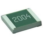
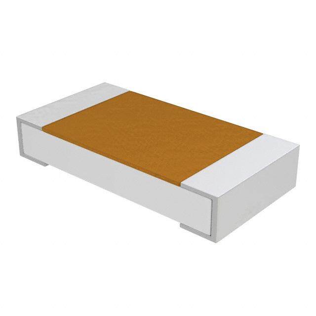
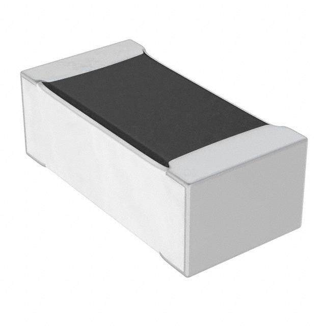
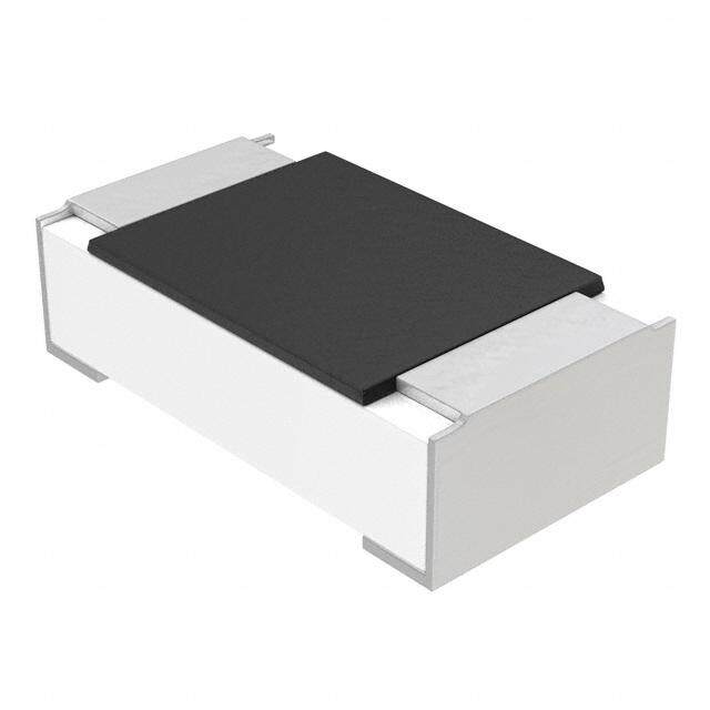
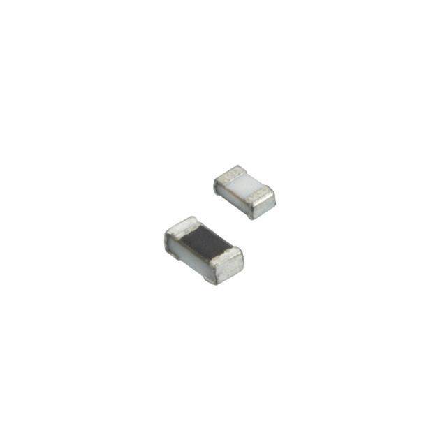
| 产品图片 |
|
| rohs | RoHS 合规性豁免无铅 / 符合限制有害物质指令(RoHS)规范要求 |
| 产品系列 | 薄膜电阻器,薄膜电阻器 - SMD,Vishay TNPW04021K50BEEDTNPW |
| 数据手册 | |
| 产品型号 | TNPW04021K50BEED |
| 产品 | Precision Resistors Thin Film SMD |
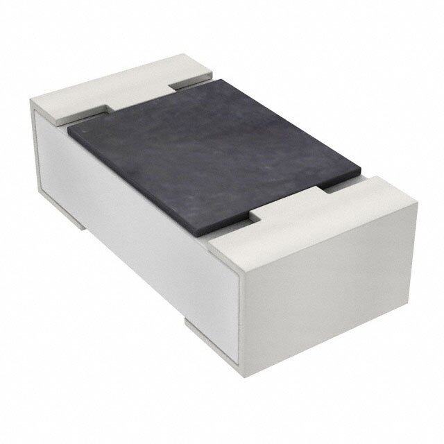
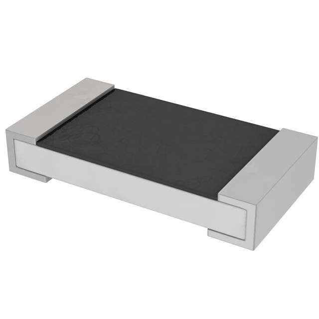
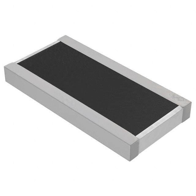
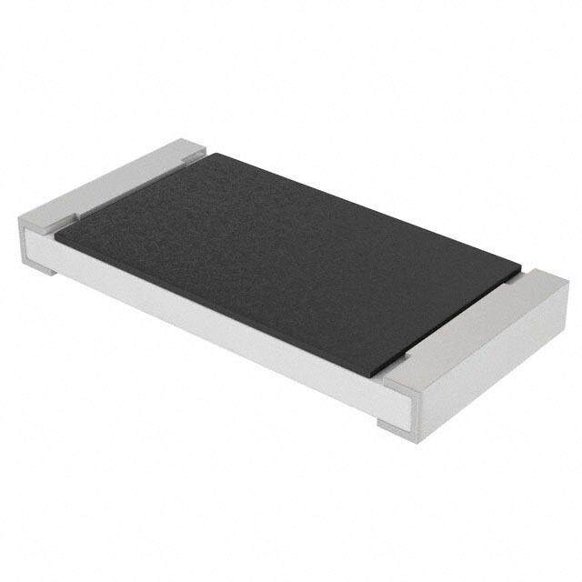
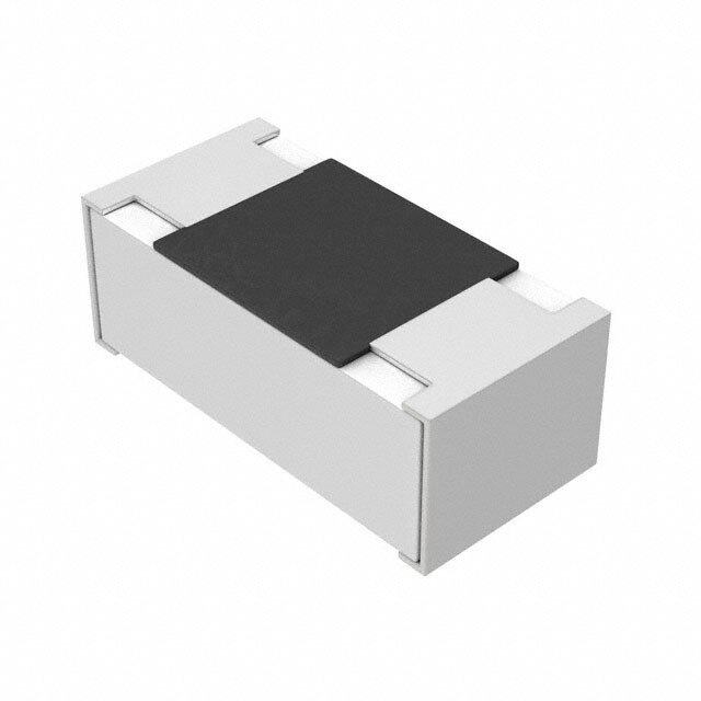
| 产品目录绘图 |
|
| 产品种类 | 薄膜电阻器 - SMD |
| 供应商器件封装 | 0402 |
| 其它名称 | TNP1.50KDADKR |
| 功率(W) | 0.063W,1/16W |
| 功率额定值 | 63 mW |
| 包装 | Digi-Reel® |
| 商标 | Vishay |
| 外壳代码-in | 0402 |
| 外壳代码-mm | 1005 |
| 外壳宽度 | 0.5 mm |
| 外壳长度 | 1 mm |
| 外壳高度 | 0.35 mm |
| 大小/尺寸 | 0.039" 长 x 0.020" 宽(1.00mm x 0.50mm) |
| 容差 | 0.1 % |
| 封装 | Reel |
| 封装/外壳 | 0402(1005 公制) |
| 封装/箱体 | 0402 (1005 metric) |
| 工作温度范围 | - 55 C to + 155 C |
| 工厂包装数量 | 10000 |
| 成分 | |
| 标准包装 | 1 |
| 温度系数 | 25 PPM / K |
| 特性 | 耐硫,获得 AEC-Q200 汽车认证、 防潮 |
| 特色产品 | http://www.digikey.com/cn/zh/ph/Vishay/tnpw.html |
| 电压额定值 | 50 V |
| 电阻 | 1.5 kOhms |
| 电阻(Ω) | 1.5k |
| 端子数 | 2 |
| 类型 | High Stability Thin Film Flat Chip Resistor |
| 系列 | TNPW |
| 高度 | 0.016"(0.40mm) |

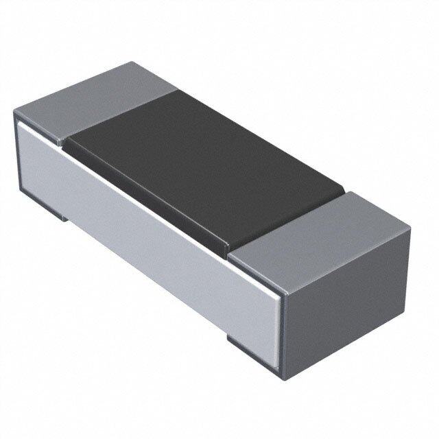
%20TNPW%20SERIES.JPG)


- 商务部:美国ITC正式对集成电路等产品启动337调查
- 曝三星4nm工艺存在良率问题 高通将骁龙8 Gen1或转产台积电
- 太阳诱电将投资9.5亿元在常州建新厂生产MLCC 预计2023年完工
- 英特尔发布欧洲新工厂建设计划 深化IDM 2.0 战略
- 台积电先进制程称霸业界 有大客户加持明年业绩稳了
- 达到5530亿美元!SIA预计今年全球半导体销售额将创下新高
- 英特尔拟将自动驾驶子公司Mobileye上市 估值或超500亿美元
- 三星加码芯片和SET,合并消费电子和移动部门,撤换高东真等 CEO
- 三星电子宣布重大人事变动 还合并消费电子和移动部门
- 海关总署:前11个月进口集成电路产品价值2.52万亿元 增长14.8%

PDF Datasheet 数据手册内容提取
TNPW e3 www.vishay.com Vishay High Stability Thin Film Flat Chip Resistors FEATURES • Superior moisture resistivity (85 °C; 85 % RH) • Excellent overall stability at different environmental conditions 0.05 % (1000 h rated power at 70 °C) • AEC-Q200 qualified • Single lot date code (optional) • Sulfur resistance verified according to ASTM B 809 • Material categorization: for definitions of complianc e please see www.vishay.com/doc?99912 APPLICATIONS TNPW e3 precision thin film flat chip resistors are the perfect • Automotive choice for most fields of modern electronics where highest reliability and stability is of major concern. Typical • Industrial equipment applications include automotive, industrial, test an d • Test and measuring equipment measuring equipment, and medical equipment. • Medical equipment TECHNICAL SPECIFICATIONS DESCRIPTION TNPW0201 e3 (1) TNPW0402 e3 TNPW0603 e3 TNPW0805 e3 TNPW1206 e3 TNPW1210 e3 Imperial size 0201 0402 0603 0805 1206 1210 Metric size code RR0603M RR1005M RR1608M RR2012M RR3216M RR3225M Resistance range 22 to 40 k 10 to 100 k 1 to 332 k 1 to 1 M 1 to 2 M 10 to 3.01 M Resistance tolerance ± 0.5 %; ± 0.1 % ± 1 %; ± 0.5 %; ± 0.1 % Temperature coefficient ± 25 ppm/K ± 50 ppm/K; ± 25 ppm/K; ± 15 ppm/K; ± 10 ppm/K Rated dissipation, P (2) 0.075 W 0.100 W 0.125 W 0.200 W 0.400 W 0.500 W 70 Operating voltage, 25 V 50 V 75 V 150 V 200 V 200 V U AC or DC max. RMS Permissible film 155 °C temperature, F max. (2) Operating temperature range -55 °C to 155 °C Internal thermal resistance (2) - 90 K/W 63 K/W 38 K/W 32 K/W - Permissible voltage against ambient (insulation): 1 min; U 50 V 75 V 100 V 200 V 300 V 300 V ins Failure rate: FITobserved 0.1 x 10⁻⁹/h Notes (1) AEC-Q200 qualification for ohmic values above 25 k pending (2) Please refer to APPLICATION INFORMATION APPLICATION INFORMATION When the resistor dissipates power, a temperature rise above the ambient temperature occurs, dependent on the thermal resistance of the assembled resistor together with the printed circuit board. The rated dissipation applies only if the permitted film temperature is not exceeded. Please consider the application note “Thermal Management in Surface-Mounted Resistor Applications ” (www.vishay.com/doc?28844) for information on the general nature of thermal resistance. These resistors do not feature a limited lifetime when operated within the permissible limits. However, resistance value drif t increasing over operating time may result in exceeding a limit acceptable to the specific application, thereby establishing a functional lifetime. Revision: 21-Feb-2020 1 Document Number: 28758 For technical questions, contact: thinfilmchip@vishay.com THIS DOCUMENT IS SUBJECT TO CHANGE WITHOUT NOTICE. THE PRODUCTS DESCRIBED HEREIN AND THIS DOCUMENT ARE SUBJECT TO SPECIFIC DISCLAIMERS, SET FORTH AT www.vishay.com/doc?91000
TNPW e3 www.vishay.com Vishay MAXIMUM RESISTANCE CHANGE AT RATED DISSIPATION OPERATION MODE STANDARD POWER TNPW0201 e3 0.050 W 0.075 W TNPW0402 e3 0.063 W 0.100 W TNPW0603 e3 0.100 W 0.125 W Rated dissipation, P 70 TNPW0805 e3 0.125 W 0.200 W TNPW1206 e3 0.250 W 0.400 W TNPW1210 e3 0.330 W 0.500 W Operating temperature range -55 °C to 125 °C -55 °C to 155 °C Permissible film temperature, F max. 125 °C 155 °C TNPW0201 e3 22 to 40 k 22 to 40 k TNPW0402 e3 10 to 100 k 10 to 100 k TNPW0603 e3 1 to 332 k 1 to 332 k TNPW0805 e3 1 to 1 M 1 to 1 M Max. resistance change at P70 for resistance range, TNPW1206 e3 1 to 2 M 1 to 2 M |R/R| after: TNPW1210 e3 10 to 3.01 M 10 to 3.01 M 1000 h 0.05 % 0.10 % 8000 h 0.10 % 0.20 % 225 000 h 0.30 % 0.60 % Note • The presented operation modes do not refer to different types of resistors, but actually show examples of different loads, that lead to different film temperatures and different achievable load-life stability (drift) of the resistance value. A suitable low thermal resistance of th e circuit board assembly must be safeguarded in order to maintain the film temperature of the resistors within the specified limits. Please consider the application note “Thermal Management in Surface-Mounted Resistor Applications” (www.vishay.com/doc?28844) for information on the general nature of thermal resistance Revision: 21-Feb-2020 2 Document Number: 28758 For technical questions, contact: thinfilmchip@vishay.com THIS DOCUMENT IS SUBJECT TO CHANGE WITHOUT NOTICE. THE PRODUCTS DESCRIBED HEREIN AND THIS DOCUMENT ARE SUBJECT TO SPECIFIC DISCLAIMERS, SET FORTH AT www.vishay.com/doc?91000
TNPW e3 www.vishay.com Vishay TEMPERATURE COEFFICIENT AND RESISTANCE RANGE TYPE / SIZE TCR TOLERANCE RESISTANCE E-SERIES ± 0.5 % 22 to 40 k TNPW0201 e3 ± 25 ppm/K E24; E192 ± 0.1 % 22 to 25 k ± 1 % E24; E96 10 to 100 k ± 50 ppm/K ± 0.5 % E24; E192 ± 0.1 % 47 to 100 k ± 1 % E24; E96 TNPW0402 e3 10 to 100 k ± 25 ppm/K ± 0.5 % ± 0.1 % E24; E192 ± 15 ppm/K 47 to 100 k ± 0.1 % ± 10 ppm/K ± 1 % E24; E96 1 to 332 k ± 50 ppm/K ± 0.5 % E24; E192 ± 0.1 % 3.5 to 332 k ± 1 % E24; E96 TNPW0603 e3 1 to 332 k ± 25 ppm/K ± 0.5 % ± 0.1 % 3.5 to 332 k E24; E192 ± 15 ppm/K ± 0.1 % 47 to 332 k ± 10 ppm/K ± 1 % E24; E96 1 to 1 M ± 50 ppm/K ± 0.5 % E24; E192 ± 0.1 % 3.5 to 1 M ± 1 % E24; E96 TNPW0805 e3 1 to 1 M ± 25 ppm/K ± 0.5 % ± 0.1 % E24; E192 ± 15 ppm/K 3.5 to 1 M ± 0.1 % ± 10 ppm/K ± 1 % E24; E96 1 to 2 M ± 50 ppm/K ± 0.5 % E24; E192 ± 0.1 % 3.5 to 2 M ± 1 % E24; E96 TNPW1206 e3 1 to 2 M ± 25 ppm/K ± 0.5 % ± 0.1 % 3.5 to 2 M E24; E192 ± 15 ppm/K ± 0.1 % 47 to 2 M ± 10 ppm/K ± 1 % E24; E96 10 to 3.01 M ± 50 ppm/K ± 0.5 % E24; E192 ± 0.1 % 47 to 2.13 M ± 1 % E24; E96 TNPW1210 e3 10 to 3.01 M ± 25 ppm/K ± 0.5 % ± 0.1 % E24; E192 ± 15 ppm/K 47 to 2.13 M ± 0.1 % ± 10 ppm/K Revision: 21-Feb-2020 3 Document Number: 28758 For technical questions, contact: thinfilmchip@vishay.com THIS DOCUMENT IS SUBJECT TO CHANGE WITHOUT NOTICE. THE PRODUCTS DESCRIBED HEREIN AND THIS DOCUMENT ARE SUBJECT TO SPECIFIC DISCLAIMERS, SET FORTH AT www.vishay.com/doc?91000
TNPW e3 www.vishay.com Vishay PACKAGING PACKAGING PACKAGING TYPE / SIZE CODE QUANTITY WIDTH PITCH STYLE DIMENSIONS TNPW0201 e3 ET7 = ED 10 000 EP1 = EP 1000 (1) 2 mm Ø 180 mm / 7" TNPW0402 e3 ET2 = EI 5000 Paper tape according ET7 = ED 10 000 8 mm IEC 60286-3, Type 1a E52 = EN 1000 (1) TNPW0603 e3 4 mm Ø 180 mm / 7" TNPW0805 e3 ET1 = EA 5000 TNPW1206 e3 TNPW1210 e3 ET6 = EC (2) 20 000 4 mm Ø 330 mm / 13" Notes (1) 1000 pieces packaging is available only for precision resistors with tolerance ± 0.1 % and temperature coefficient ± 25 ppm/K (2) 20 000 pieces packaging is available only for resistors with TCR ± 25 ppm/K and ± 50 ppm/K PART NUMBER AND PRODUCT DESCRIPTION Part Number: TNPW12061K32DEEA T N P W 1 2 0 6 1 K 3 2 D E E A TYPE / SIZE RESISTANCE TOLERANCE TCR PACKAGING SPECIAL TNPW0201 R = decimal B = ± 0.1 % H = ± 50 ppm/K ED Up to 2 digits TNPW0402 K = thousand D = ± 0.5 % E = ± 25 ppm/K EP Blank = standard TNPW0603 M = million F = ± 1.0 % X = ± 15 ppm/K EI 0H = single lot date TNPW0805 (4 digits) Y = ± 10 ppm/K EN code TNPW1206 EA TNPW1210 EC (E.. = lead-free) Product Description: TNPW1206 1K32 0.5 % T-9 ET1 e3 TNPW1206 1K32 0.5 % T-9 ET1 e3 TYPE / SIZE RESISTANCE TOLERANCE TCR PACKAGING LEAD (Pb)-FREE TNPW0201 54R1 = 54.1 ± 0.1 % T-2 = ± 50 ppm/K ET7 e3 = pure matte tin TNPW0402 1K32 = 1320 ± 0.5 % T-9 = ± 25 ppm/K EP1 termination finish TNPW0603 ± 1.0 % T-10 = ± 15 ppm/K ET2 TNPW0805 T-13 = ± 10 ppm/K E52 BV 20545 = single TNPW1206 ET1 lot date code TNPW1210 ET6 (E.. = lead-free) Note • The product can be ordered using either the PART NUMBER or the PRODUCT DESCRIPTION Revision: 21-Feb-2020 4 Document Number: 28758 For technical questions, contact: thinfilmchip@vishay.com THIS DOCUMENT IS SUBJECT TO CHANGE WITHOUT NOTICE. THE PRODUCTS DESCRIBED HEREIN AND THIS DOCUMENT ARE SUBJECT TO SPECIFIC DISCLAIMERS, SET FORTH AT www.vishay.com/doc?91000
TNPW e3 www.vishay.com Vishay DESCRIPTION MATERIALS Production is strictly controlled and follows an extensive se t Vishay acknowledges the following systems for th e of instructions established for reproducibility. A regulation of hazardous substances: homogeneous film of special metal alloy is deposited on a • IEC 62474, Material Declaration for Products of and for the high grade ceramic substrate (AI2O3) and conditioned to Electrotechnical Industry, with the list of declarable achieve the desired temperature coefficient. Speciall y substances given therein (2) designed inner contacts are deposited on both sides. A • The Global Automotive Declarable Substance Lis t special laser is used to achieve the target value by smoothly (GADSL) (3) fine trimming the resistive layer without damaging the • The REACH regulation (1907/2006/EC) and the related lis t ceramics. A further conditioning is applied in order t o of substances with very high concern (SVHC) (4) for its stabilize the trimming result. The resistor elements are supply chain covered by a protective coating designed for electrical, The products do not contain any of the banned substances mechanical and climatic protection. The termination s as per IEC 62474, GADSL, or the SVHC list, see receive a final pure matte tin on nickel plating. www.vishay.com/how/leadfree. The result of the determined production is verified by an Hence the products fully comply with the following extensive testing procedure and optical inspection directives: performed on 100 % of the individual chip resistors. Thi s includes full screening for the elimination of products with a • 2000/53/EC End-of-Life Vehicle Directive (ELV) and potential risk of early life failures (feasible for R 10 ). Only Annex II (ELV II) accepted products are laid directly into the tape i n • 2011/65/EU Restriction of the Use of Hazardous accordance with IEC 60286-3, Type 1a (1). Substances Directive (RoHS) with amendmen t 2015/863/EU ASSEMBLY • 2012/19/EU Waste Electrical and Electronic Equipment The resistors are suitable for processing on automatic SMD Directive (WEEE) assembly systems. They are suitable for automatic Vishay pursues the elimination of conflict minerals from its soldering using wave, reflow or vapour phase as shown i n supply chain, see the Conflict Minerals Policy a t IEC 61760-1 (1). The encapsulation is resistant to all www.vishay.com/doc?49037. cleaning solvents commonly used in the electronics industry, including alcohols, esters and aqueous solutions. RELATED PRODUCTS The suitability of conformal coatings, potting compounds The TNPW with SnPb termination plating is designed for and their processes, if applied, shall be qualified b y those applications, where lead bearing terminations ar e appropriate means to ensure the long-term stability of th e mandatory. For ordering TNPW with SnPb terminations whole system. please refer to latest edition of datasheet TNPW The resistors are RoHS-compliant, the pure matte tin plating (www.vishay.com/doc?31006). provides compatibility with lead (Pb)-free an d TNPU e3 ultra precision thin film flat chip resistors combine lead-containing soldering processes. Solderability is the proven reliability of TNPW e3 products with a most specified for 2 years after production or requalification. The advanced level of precision and stabilit y permitted storage time is 20 years. The immunity of th e (www.vishay.com/doc?28779). plating against tin whisker growth has been proven unde r TNPS .... ESCC high-reliability thin film chip resistors are the extensive testing. premium choice for design and manufacture of equipment , where matured technology and proven reliability are of utmost importance. They are regularly used i n communication and research satellites and fit equally well into aircraft and military electronic systems. Approval of the TNPS .... ESCC products is granted by th e European Space Components Coordination and registered in the ESCC Qualified Parts List, REP005 (www.vishay.com/doc?28789). TNPV e3 High Voltage Thin Film Flat Chip Resistors are designed for most fields of modern electronics wher e precision, reliability and stability at high operating voltage are primary concerns (www.vishay.com/doc?28881). Notes (1) The quoted IEC standards are also released as EN standards with the same number and identical contents (2) The IEC 62474 list of declarable substances is maintained in a dedicated database, which is available at http://std.iec.ch/iec62474 (3) The Global Automotive Declarable Substance List (GADSL) is maintained by the American Chemistry Council and available at www.gadsl.org (4) The SVHC list is maintained by the European Chemical Agency (ECHA) and available at http://echa.europa.eu/candidate-list-table Revision: 21-Feb-2020 5 Document Number: 28758 For technical questions, contact: thinfilmchip@vishay.com THIS DOCUMENT IS SUBJECT TO CHANGE WITHOUT NOTICE. THE PRODUCTS DESCRIBED HEREIN AND THIS DOCUMENT ARE SUBJECT TO SPECIFIC DISCLAIMERS, SET FORTH AT www.vishay.com/doc?91000
TNPW e3 www.vishay.com Vishay FUNCTIONAL PERFORMANCE B 3 n d120 V/V 2 on-Linearity iA311910000 TTTTNNNNPPPPWWWW1000286400006532 eeee3333 µurrent Noise in 00..153 TNPW0402 e3 TNTPNWP0W600830 e53 e 3 N C 0.1 TNPW1206 e3 80 0.05 0.03 70 60 0.01 10 100 1K 10K 100K 100 1K 10K 100K 1M Resistance Value in Ω Resistance Value in Ω Non-Linearity Current Noise 60 60 ϑ° TNPW0603 e3 % TNPW0603 e3 se Angle in 2400 10 Ω [Z]-RO inRO4200 10 Ω ha 0 0 100 Ω P 100 Ω 1 k Ω - 20 1 k Ω - 40 - 40 4.75 k Ω - 60 4.75 k Ω - 60 10 k Ω -80 10 k Ω -80 1 5 10 50100 500 1000 1 5 10 50 100 500 1000 Frequency f in MHz Frequency f in MHz HF Performance (1) HF Performance (1) 60 60 ϑ° TNPW0805 e3 % TNPW0805 e3 n 40 n 40 e i O i gl RO se An 20 10 Ω [Z]-R20 10 Ω Pha 0 100 Ω 0 110 0k ΩΩ - 20 - 20 1 k Ω - 40 - 40 - 60 - 60 10 k Ω -80 10 k Ω -80 1 5 10 50 100 500 1000 1 5 10 50 100 500 1000 Frequency f in MHz Frequency f in MHz HF Performance (1) HF Performance (1) Note (1) Typical figures. HF-characteristic also depends on termination and circuit design Revision: 21-Feb-2020 6 Document Number: 28758 For technical questions, contact: thinfilmchip@vishay.com THIS DOCUMENT IS SUBJECT TO CHANGE WITHOUT NOTICE. THE PRODUCTS DESCRIBED HEREIN AND THIS DOCUMENT ARE SUBJECT TO SPECIFIC DISCLAIMERS, SET FORTH AT www.vishay.com/doc?91000
TNPW e3 www.vishay.com Vishay FUNCTIONAL PERFORMANCE 0.6 P n W TNPW0201 e3 patio 0.5 TTNNPPWW00460023 ee33 si TNPW0805 e3 Dis 0.4 TNPW1206 e3 er TNPW1210 e3 w 0.3 o P 0.2 0.1 0 -55 0 50 100 125 °C 155 70 Ambient Temparature ϑ amb Derating - Standard Operation 0.6 P n W TNPW0201 e3 patio 0.5 TTNNPPWW00460023 ee33 si TNPW0805 e3 Dis 0.4 TNPW1206 e3 er TNPW1210 e3 w 0.3 o P 0.2 0.1 0 -55 0 50 100 125 °C 155 70 Ambient Temparature ϑ amb Derating - Power Operation Note • The solid line is based on IEC/EN reference test conditions which is considered as standard mode. However, above that the maximu m permissible film temperature is 155 °C (dashed line) Revision: 21-Feb-2020 7 Document Number: 28758 For technical questions, contact: thinfilmchip@vishay.com THIS DOCUMENT IS SUBJECT TO CHANGE WITHOUT NOTICE. THE PRODUCTS DESCRIBED HEREIN AND THIS DOCUMENT ARE SUBJECT TO SPECIFIC DISCLAIMERS, SET FORTH AT www.vishay.com/doc?91000
TNPW e3 www.vishay.com Vishay FUNCTIONAL PERFORMANCE V 3K V 3K age in 1K TNPW0805 e3 age in 1K TNPW0805 e3 olt olt V V st TNPW0603 e3 st e e T T TNPW0603 e3 100 100 10 10 10R 100R 1K 10K 100K 10R 100R 1K 10K 100K Resistance VainluΩe Resistance VainluΩe Single-Pulse High Voltage Overload Single-Pulse High Voltage Overload Test 1.2/50 μs EN140000 4.27 Test 10/700 μs EN140000 4.27 100W 100W Pi, max. TTNNPPWW10820056 ee33 Pi, max. TNPW1206 e3 wer 10W TNPW0603 e3 wer 10W TNPW0805 e3 o o p p TNPW0603 e3 e e s s ul ul p p e e bl 1W bl 1W si si s s mi mi Conditions: er Conditions: er P ≤P (including derating) P P 0, n ≤ 1000 and Ui≤Ui, max. P anmdaxU.i≤mUaix, .max. 0.1W 0.1W 10 µs 100 µs 1 ms 10 ms 100 ms 1 s 10 s 10 µs 100 µs 1 ms 10 ms 100 ms 1 s 10 s Pulse Duration t Pulse Duration t i i Maximum Pulse Load P Maximum Pulse Load P i, max. i, max. for Single Pulses for Continuous Pulses 10 000 V max. Ui, e g olta1000V TNPW1206 e3 v se TNPW0805 e3 ul p TNPW0603 e3 e bl 100V si s mi er Conditions: P P≤P i i, max. 10V 10 µs 100 µs 1 ms 10 ms 100 ms 1 s 10 s Pulse Duration t i Maximum Pulse Voltage U i, max. Revision: 21-Feb-2020 8 Document Number: 28758 For technical questions, contact: thinfilmchip@vishay.com THIS DOCUMENT IS SUBJECT TO CHANGE WITHOUT NOTICE. THE PRODUCTS DESCRIBED HEREIN AND THIS DOCUMENT ARE SUBJECT TO SPECIFIC DISCLAIMERS, SET FORTH AT www.vishay.com/doc?91000
TNPW e3 www.vishay.com Vishay TEST AND REQUIREMENTS All tests are carried out in accordance with the following The testing also covers most of the requirements specifie d specifications: by EIA / ECA-703 and JIS-C-5201-1. EN 60115-1, generic specification The tests are carried out under standard atmospheri c EN 60115-8 (successor of EN 140400), sectional conditions in accordance with IEC 60068-1, 4.3, whereupon specification the following values are applied: EN 140401-801, detail specification Temperature: 15 °C to 35 °C IEC 60068-2-xx, test methods Relative humidity: 25 % to 75 % The parameters stated in the Test Procedures an d Air pressure: 86 kPa to 106 kPa (860 mbar to 1060 mbar) Requirements table are based on the required tests and A climatic category LCT / UCT / 56 is applied, defined by the permitted limits of EN 140401-801. The detail specification lower category temperature (LCT), the upper categor y EN 140401-801 does not cover case size 0201. The table temperature (UCT), and the duration of exposure in th e damp heat, steady state test (56 days). presents only the most important tests, for the full test schedule refer to the documents listed above. However, The components are mounted for testing on printed circuit boards in accordance with EN 60115-8, 2.4.2, unless some additional tests and a number of improvements otherwise specified. against those minimum requirements have been included. TEST PROCEDURES AND REQUIREMENTS EN 60115-1 IEC 60068-2 (1) REQUIREMENTS TEST PROCEDURE CLAUSE TEST METHOD PERMISSIBLE CHANGE (R) Stability for product types: TNPW0201 e3 22 to 40 k TNPW0402 e3 10 to 100 k TNPW0603 e3 1 to 332 k TNPW0805 e3 1 to 1 M TNPW1206 e3 1 to 2 M TNPW1210 e3 10 to 3.01 M 4.5 - Resistance - ± 1 %; ± 0.5 %; ± 0.1 % Temperature At (20 / -55 / 20) °C ± 50 ppm/K; ± 25 ppm/K; 4.8 - coefficient and (20 / 125 / 20) °C ± 15 ppm/K; ± 10 ppm/K U = P x R or U = U ; Endurance 70 max. whichever is the less severe; at 70 °C: 1.5 h on; 0.5 h off; standard operation 70 °C; 1000 h ± (0.05 % R + 0.01 ) mode 70 °C; 8000 h ±(0.1 % R + 0.02 ) 4.25.1 - U = P x R or U = U ; Endurance 70 max. whichever is the less severe; at 70 °C: 1.5 h on; 0.5 h off; power operation 70 °C; 1000 h ± (0.1 % R + 0.01 ) mode 70 °C; 8000 h ±(0.2 % R + 0.02 ) Endurance at 125 °C; 1000 h ± (0.05 % R + 0.01 ) 4.25.3 - upper category temperature 155 °C; 1000 h ± (0.1 % R + 0.02 ) Damp heat, (40 ± 2) °C; 56 days; 4.24 78 (Cab) ± (0.1 % R + 0.01 ) steady state (93 ± 3) % RH Damp heat, steady state (85 ± 2) °C accelerated: (85 ± 5) % RH 4.37 67 (Cy) ± (0.25 % R + 0.05 ) Standard U = 0.1 x P x R; 70 operation U 0.3 x Umax.; 1000 h mode - 1 (Ab) Cold -55 °C; 2 h ± (0.05 % R + 0.01 ) Revision: 21-Feb-2020 9 Document Number: 28758 For technical questions, contact: thinfilmchip@vishay.com THIS DOCUMENT IS SUBJECT TO CHANGE WITHOUT NOTICE. THE PRODUCTS DESCRIBED HEREIN AND THIS DOCUMENT ARE SUBJECT TO SPECIFIC DISCLAIMERS, SET FORTH AT www.vishay.com/doc?91000
TNPW e3 www.vishay.com Vishay TEST PROCEDURES AND REQUIREMENTS EN 60115-1 IEC 60068-2 (1) REQUIREMENTS TEST PROCEDURE CLAUSE TEST METHOD PERMISSIBLE CHANGE (R) Stability for product types: TNPW0201 e3 22 to 40 k TNPW0402 e3 10 to 100 k TNPW0603 e3 1 to 332 k TNPW0805 e3 1 to 1 M TNPW1206 e3 1 to 2 M TNPW1210 e3 10 to 3.01 M 30 min at LCT and 30 min at UCT; Rapid change 4.19 14 (Na) LCT = - 55 °C; UCT = 125 °C; ± (0.1 % R + 0.01 ) of temperature 1000 cycles Short time U = 2.5 x P x R overload: 70 or U = 2 x U ; standard max. ± (0.05 % R + 0.01 ) whichever is the less severe; operation 5 s mode 4.13 - Short time U = 2.5 x P x R overload: 70 or U = 2 x U ; power max. ± (0.1 % R + 0.01 ) whichever is the less severe; operation 5 s mode Single pulse Severity no. 4: high voltage U = 10 x P x R or overload: 70 ± (0.5 % R + 0.02 ) U = 2 x U ; standard max. no visible damage operation whichever is the less severe; mode 10 pulses 10 μs/700 μs 4.27 - Single pulse Severity no. 4: high voltage U = 10 x P x R or overload: 70 ± (1 % R + 0.02 ) U = 2 x U ; power max. no visible damage operation whichever is the less severe; mode 10 pulses 10 μs/700 μs Periodic U = 15 x P x R electric 70 or U = 2 x U ; overload: max. ± (0.5 % R + 0.05 ) 0.1 s on; 2.5 s off; standard no visible damage whichever is the less severe; operation 1000 cycles mode 4.39 - Periodic U = 15 x P x R electric 70 or U = 2 x U ; overload: max. ± (1 % R + 0.05 ) 0.1 s on; 2.5 s off; power no visible damage whichever is the less severe; operation 1000 cycles mode IEC 61340-3-1 (1); 3 pos. + 3 neg. (equivalent to MIL-STD-883, method Electro static 3015) discharge 4.38 - TNPW0201 e3: 200 V ±(0.5 % R + 0.05 ) (human body TNPW0402 e3: 400 V model) TNPW0603 e3: 1000 V TNPW0805 e3: 1500 V TNPW 1206 e3: 2000 V Endurance by sweeping; 10 Hz to 2000 Hz; ± (0.05 % R + 0.01 ) 4.22 6 (Fc) Vibration no resonance; no visible damage amplitude 1.5 mm or 200 m/s2; 7.5 h Revision: 21-Feb-2020 10 Document Number: 28758 For technical questions, contact: thinfilmchip@vishay.com THIS DOCUMENT IS SUBJECT TO CHANGE WITHOUT NOTICE. THE PRODUCTS DESCRIBED HEREIN AND THIS DOCUMENT ARE SUBJECT TO SPECIFIC DISCLAIMERS, SET FORTH AT www.vishay.com/doc?91000
TNPW e3 www.vishay.com Vishay TEST PROCEDURES AND REQUIREMENTS EN 60115-1 IEC 60068-2 (1) REQUIREMENTS TEST PROCEDURE CLAUSE TEST METHOD PERMISSIBLE CHANGE (R) Stability for product types: TNPW0201 e3 22 to 40 k TNPW0402 e3 10 to 100 k TNPW0603 e3 1 to 332 k TNPW0805 e3 1 to 1 M TNPW1206 e3 1 to 2 M TNPW1210 e3 10 to 3.01 M Solder bath method; SnPb40; non-activated flux (215 ± 3) °C; (3 ± 0.3) s Good tinning ( 95 % covered); 4.17 58 (Td) Solderability Solder bath method; no visible damage SnAg3Cu0.5 or SnAg3.5; non-activated flux (235 ± 3) °C; (2 ± 0.2) s Resistance to Solder bath method; 4.18 58 (Td) ± (0.02 % R + 0.01 ) soldering heat (260 ± 5) °C; (10 ± 1) s (2) Component 4.29 45 (XA) solvent Isopropyl alcohol + 50 °C; method 2 No visible damage resistance TNPW0201 e3: 2 N Shear 4.32 21 (Ue ) TNPW0402 e3 and TNPW0603 e3: 9 N No visible damage 3 (adhesion) TNPW0805 e3 and TNPW1206 e3: 45 N ± (0.05 % R + 0.01 ) Substrate 4.33 21 (Ue ) Depth 2 mm, 3 times no visible damage, 1 bending no open circuit in bent position 4.7 - Voltage proof U = U ; 60 ± 5 s No flashover or breakdown RMS ins IEC 60695-11-5 (1), 4.35 - Flammability No burning after 30 s needle flame test; 10 s Notes (1) The quoted IEC standards are also released as EN standards with the same number and identical contents (2) For TNPW0201 e3 only similar to DIN EN 60115-8 test procedure. Due to the components small size they were fixed by glue previous to testing instead of applying tweezers Revision: 21-Feb-2020 11 Document Number: 28758 For technical questions, contact: thinfilmchip@vishay.com THIS DOCUMENT IS SUBJECT TO CHANGE WITHOUT NOTICE. THE PRODUCTS DESCRIBED HEREIN AND THIS DOCUMENT ARE SUBJECT TO SPECIFIC DISCLAIMERS, SET FORTH AT www.vishay.com/doc?91000
TNPW e3 www.vishay.com Vishay DIMENSIONS L T t W H T b DIMENSIONS AND MASS L W H T / T MASS TYPE / SIZE t b (mm) (mm) (mm) (mm) (mg) TNPW0201 e3 0.6 ± 0.05 0.3 ± 0.05 0.23 ± 0.03 0.12 ± 0.05 0.14 TNPW0402 e3 1.0 ± 0.05 0.5 ± 0.05 0.35 ± 0.05 0.2 ± 0.10 0.65 TNPW0603 e3 1.55 ± 0.05 0.85 ± 0.10 0.45 ± 0.10 0.3 ± 0.20 2 TNPW0805 e3 2.0 ± 0.1 1.25 ± 0.15 0.45 ± 0.10 0.4 ± 0.20 5.5 TNPW1206 e3 3.2 + 0.1 / - 0.2 1.6 ± 0.15 0.55 ± 0.10 0.5 ± 0.25 10 TNPW1210 e3 3.2 + 0.1 / - 0.2 2.45 ± 0.15 0.60 ± 0.15 0.5 ± 0.25 16 SOLDER PAD DIMENSIONS l b a RECOMMENDED SOLDER PAD DIMENSIONS REFLOW SOLDERING WAVE SOLDERING TYPE / SIZE a b l a b l (mm) (mm) (mm) (mm) (mm) (mm) TNPW0201 e3 0.28 0.43 0.23 - - - TNPW0402 e3 0.4 0.6 0.5 - - - TNPW0603 e3 0.5 0.9 1.0 0.9 0.9 1.0 TNPW0805 e3 0.7 1.3 1.2 0.9 1.3 1.3 TNPW1206 e3 0.9 1.7 2.0 1.1 1.7 2.3 TNPW1210 e3 0.9 2.5 2.0 1.1 2.5 2.3 Revision: 21-Feb-2020 12 Document Number: 28758 For technical questions, contact: thinfilmchip@vishay.com THIS DOCUMENT IS SUBJECT TO CHANGE WITHOUT NOTICE. THE PRODUCTS DESCRIBED HEREIN AND THIS DOCUMENT ARE SUBJECT TO SPECIFIC DISCLAIMERS, SET FORTH AT www.vishay.com/doc?91000
Legal Disclaimer Notice www.vishay.com Vishay Disclaimer ALL PRODUCT, PRODUCT SPECIFICATIONS AND DATA ARE SUBJECT TO CHANGE WITHOUT NOTICE TO IMPROV E RELIABILITY, FUNCTION OR DESIGN OR OTHERWISE. Vishay Intertechnology, Inc., its affiliates, agents, and employees, and all persons acting on its or their behalf (collectively, “Vishay”), disclaim any and all liability for any errors, inaccuracies or incompleteness contained in any datasheet or in any other disclosure relating to any product. Vishay makes no warranty, representation or guarantee regarding the suitability of the products for any particular purpose o r the continuing production of any product. To the maximum extent permitted by applicable law, Vishay disclaims (i) any and all liability arising out of the application or use of any product, (ii) any and all liability, including without limitation special, consequential or incidental damages, and (iii) any and all implied warranties, including warranties of fitness for particular purpose, non-infringement and merchantability. Statements regarding the suitability of products for certain types of applications are based on Vishay’s knowledge of typical requirements that are often placed on Vishay products in generic applications. Such statements are not binding statements about the suitability of products for a particular application. It is the customer’s responsibility to validate that a particular product with the properties described in the product specification is suitable for use in a particular application. Parameters provided in datasheets and / or specifications may vary in different applications and performance may vary over time. All operating parameters, including typical parameters, must be validated for each customer application by the customer’s technical experts. Product specifications do not expand or otherwise modify Vishay’s terms and conditions of purchase, including but not limited to the warranty expressed therein. Except as expressly indicated in writing, Vishay products are not designed for use in medical, life-saving, or life-sustainin g applications or for any other application in which the failure of the Vishay product could result in personal injury or death. Customers using or selling Vishay products not expressly indicated for use in such applications do so at their own risk . Please contact authorized Vishay personnel to obtain written terms and conditions regarding products designed for such applications. No license, express or implied, by estoppel or otherwise, to any intellectual property rights is granted by this documen t or by any conduct of Vishay. Product names and markings noted herein may be trademarks of their respective owners. © 2019 VISHAY INTERTECHNOLOGY, INC. ALL RIGHTS RESERVED Revision: 01-Jan-2019 1 Document Number: 91000