ICGOO在线商城 > 集成电路(IC) > 嵌入式 - 微控制器 > TMS320F28069UPNT
 Datasheet下载
- 型号: TMS320F28069UPNT
- 制造商: Texas Instruments
- 库位|库存: xxxx|xxxx
- 要求:
| 数量阶梯 | 香港交货 | 国内含税 |
| +xxxx | $xxxx | ¥xxxx |
查看当月历史价格
查看今年历史价格
TMS320F28069UPNT产品简介:
ICGOO电子元器件商城为您提供TMS320F28069UPNT由Texas Instruments设计生产,在icgoo商城现货销售,并且可以通过原厂、代理商等渠道进行代购。 TMS320F28069UPNT价格参考。Texas InstrumentsTMS320F28069UPNT封装/规格:嵌入式 - 微控制器, C28x 微控制器 IC C2000™ C28x Piccolo™ 32-位 90MHz 256KB(128K x 16) 闪存 80-LQFP(12x12)。您可以下载TMS320F28069UPNT参考资料、Datasheet数据手册功能说明书,资料中有TMS320F28069UPNT 详细功能的应用电路图电压和使用方法及教程。
Texas Instruments(德州仪器)的TMS320F28069UPNT是一款高性能、低功耗的嵌入式微控制器,属于C2000系列。该型号广泛应用于需要实时控制和高效处理能力的各种工业和消费类场景中。以下是其主要应用场景:

1. 电机控制:TMS320F28069UPNT在电机控制领域表现出色,适用于交流感应电机(ACIM)、无刷直流电机(BLDC)、永磁同步电机(PMSM)等。它提供高精度的PWM输出、快速响应的ADC采样以及丰富的外设接口,能够实现高效的矢量控制(FOC)和直接转矩控制(DTC),从而优化电机性能并提高能效。

2. 电源管理:该微控制器可用于开关电源(SMPS)、逆变器、不间断电源(UPS)等电力电子设备。其内置的高速运算放大器、比较器和模拟前端(AFE)有助于精确监控电压电流变化,确保系统的稳定性和安全性。

3. 太阳能逆变器:在可再生能源领域,TMS320F28069UPNT可以用于太阳能光伏逆变器的设计。通过先进的算法和控制策略,它可以最大化能量转换效率,同时支持多种通信协议以便于远程监控与维护。

4. 伺服驱动系统:对于精密机械臂、数控机床等自动化设备中的伺服驱动系统,这款微控制器提供了强大的计算能力和灵活的I/O配置,能够满足复杂运动轨迹规划和实时反馈调节的需求。

5. 智能家电:如空调、洗衣机、冰箱等家用电器也越来越多地采用这类高性能微控制器来提升用户体验。例如,它可以实现更精准的温度控制、更低的噪音水平以及更好的节能效果。

总之,TMS320F28069UPNT凭借其卓越的性能和广泛的适用性,在众多涉及实时控制的应用场合中发挥着重要作用。
| 参数 | 数值 |
| 产品目录 | 集成电路 (IC)半导体 |
| 描述 | IC MCU 32BIT 256KB FLASH 80LQFP32位微控制器 - MCU PICCOLO MCU |
| EEPROM容量 | - |
| 产品分类 | |
| I/O数 | 40 |
| 品牌 | Texas Instruments |
| 产品手册 | |
| 产品图片 |
|
| rohs | 符合RoHS无铅 / 符合限制有害物质指令(RoHS)规范要求 |
| 产品系列 | 嵌入式处理器和控制器,微控制器 - MCU,32位微控制器 - MCU,Texas Instruments TMS320F28069UPNTC2000™ C28x Piccolo™ |
| 数据手册 | |
| 产品型号 | TMS320F28069UPNT |
| RAM容量 | 50K x 16 |
| 产品培训模块 | http://www.digikey.cn/PTM/IndividualPTM.page?site=cn&lang=zhs&ptm=25065http://www.digikey.cn/PTM/IndividualPTM.page?site=cn&lang=zhs&ptm=25227http://www.digikey.cn/PTM/IndividualPTM.page?site=cn&lang=zhs&ptm=25870http://www.digikey.cn/PTM/IndividualPTM.page?site=cn&lang=zhs&ptm=30354 |
| 产品种类 | 32位微控制器 - MCU |
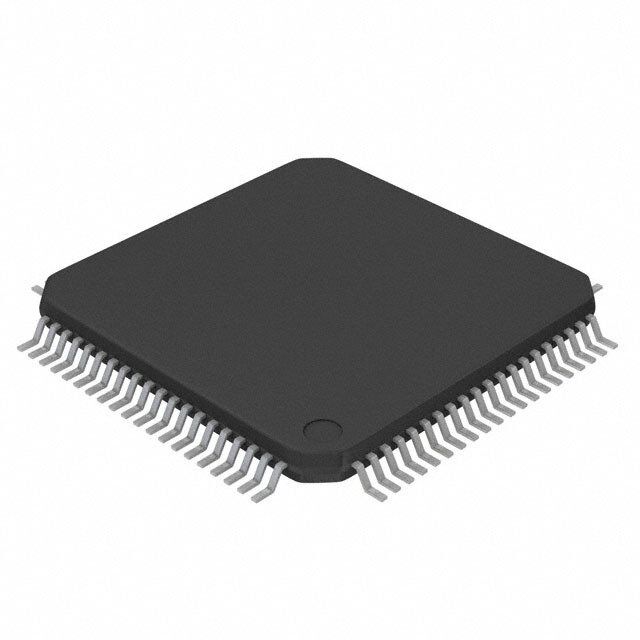
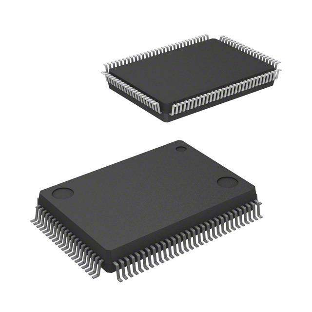
| 供应商器件封装 | 80-LQFP(12x12) |
| 其它名称 | 296-35699 |
| 制造商产品页 | http://www.ti.com/general/docs/suppproductinfo.tsp?distId=10&orderablePartNumber=TMS320F28069UPNT |
| 包装 | 托盘 |
| 可编程输入/输出端数量 | 40 |
| 商标 | Texas Instruments |
| 商标名 | Piccolo |
| 处理器系列 | Piccolo |
| 外设 | 欠压检测/复位,DMA,POR,PWM,WDT |
| 安装风格 | SMD/SMT |
| 定时器数量 | 3 Timer |
| 封装/外壳 | 80-LQFP |
| 封装/箱体 | LQFP-80 |
| 工作温度 | -40°C ~ 105°C |
| 工作电源电压 | 1.8 V, 3.3 V |
| 工厂包装数量 | 119 |
| 振荡器类型 | 内部 |
| 接口类型 | CAN/I2C/SCI/SPI/UART/USB |
| 数据RAM大小 | 50 kB |
| 数据总线宽度 | 32 bit |
| 数据转换器 | A/D 12x12b |
| 最大工作温度 | + 105 C |
| 最大时钟频率 | 80 MHz |
| 最小工作温度 | - 40 C |
| 标准包装 | 119 |
| 核心 | C28x |
| 核心处理器 | C28x |
| 核心尺寸 | 32-位 |
| 片上ADC | Yes |
| 电压-电源(Vcc/Vdd) | 1.71 V ~ 1.995 V |
| 程序存储器大小 | 128 kB |
| 程序存储器类型 | 闪存 |
| 程序存储容量 | 256KB(128K x 16) |
| 系列 | TMS320F28069 |
| 输入/输出端数量 | 40 I/O |
| 连接性 | CAN, I²C, McBSP, SCI, SPI, UART/USART, USB |
| 速度 | 90MHz |


- 商务部:美国ITC正式对集成电路等产品启动337调查
- 曝三星4nm工艺存在良率问题 高通将骁龙8 Gen1或转产台积电
- 太阳诱电将投资9.5亿元在常州建新厂生产MLCC 预计2023年完工
- 英特尔发布欧洲新工厂建设计划 深化IDM 2.0 战略
- 台积电先进制程称霸业界 有大客户加持明年业绩稳了
- 达到5530亿美元!SIA预计今年全球半导体销售额将创下新高
- 英特尔拟将自动驾驶子公司Mobileye上市 估值或超500亿美元
- 三星加码芯片和SET,合并消费电子和移动部门,撤换高东真等 CEO
- 三星电子宣布重大人事变动 还合并消费电子和移动部门
- 海关总署:前11个月进口集成电路产品价值2.52万亿元 增长14.8%


PDF Datasheet 数据手册内容提取
Product Order Technical Tools & Support & Folder Now Documents Software Community TMS320F28069,TMS320F28069F,TMS320F28069M,TMS320F28068F,TMS320F28068M TMS320F28067,TMS320F28066,TMS320F28065,TMS320F28064 TMS320F28063,TMS320F28062,TMS320F28062F SPRS698H–NOVEMBER2010–REVISEDMARCH2020 TMS320F2806x Microcontrollers 1 Device Overview 1.1 Features 1 • High-efficiency32-bitCPU(TMS320C28x) • Upto8EnhancedPulse-WidthModulator(ePWM) – 90MHz(11.11-nscycletime) modules – 16× 16and32×32MultiplyandAccumulate – 16PWMchannelstotal(8HRPWM-capable) (MAC)operations – Independent16-bittimerineachmodule – 16× 16dualMAC • ThreeinputEnhancedCapture(eCAP)modules – Harvardbusarchitecture • Upto4High-ResolutionCapture(HRCAP) – Atomicoperations modules – Fastinterruptresponseandprocessing • Upto2EnhancedQuadratureEncoderPulse (eQEP)modules – Unifiedmemoryprogrammingmodel • 12-bitAnalog-to-DigitalConverter(ADC),dual – Code-efficient(inC/C++andAssembly) Sample-and-Hold(S/H) • Floating-PointUnit(FPU) – Upto3.46MSPS – Nativesingle-precisionfloating-pointoperations – Upto16channels • ProgrammableControlLawAccelerator(CLA) • On-chiptemperaturesensor – 32-bitfloating-pointmathaccelerator • 128-bitsecuritykeyandlock – ExecutescodeindependentlyofthemainCPU – Protectssecurememoryblocks • Viterbi,ComplexMath,CRCUnit(VCU) – Preventsreverse-engineeringoffirmware – ExtendsC28xinstructionsettosupportcomplex • Serialportperipherals multiply,Viterbioperations,andCyclic RedundencyCheck(CRC) – TwoSerialCommunicationsInterface(SCI) [UART]modules • Embeddedmemory – TwoSerialPeripheralInterface(SPI)modules – Upto256KBofflash – OneInter-Integrated-Circuit(I2C)bus – Upto100KBofRAM – OneMultichannelBufferedSerialPort(McBSP) – 2KBofOne-TimeProgrammable(OTP)ROM bus • 6-channelDirectMemoryAccess(DMA) – OneEnhancedControllerAreaNetwork(eCAN) • Lowdeviceandsystemcost – UniversalSerialBus(USB)2.0 – Single3.3-Vsupply (seeDeviceComparisonforavailability) – Nopowersequencingrequirement – Full-speeddevicemode – Integratedpower-onresetandbrownoutreset – Full-speedorlow-speedhostmode – Low-poweroperatingmodes • Upto54individuallyprogrammable,multiplexed – Noanalogsupportpin General-PurposeInput/Output(GPIO)pinswith • Endianness:Littleendian inputfiltering • JTAGboundaryscansupport • Advancedemulationfeatures – IEEEStandard1149.1-1990StandardTest – Analysisandbreakpointfunctions AccessPortandBoundaryScanArchitecture – Real-timedebugthroughhardware • Clocking • Packageoptions – Twointernalzero-pinoscillators – 80-pinPFPand100-pinPZP PowerPAD™ – On-chipcrystaloscillator/externalclockinput ThermallyEnhancedThinQuadFlatpacks – Watchdogtimermodule (HTQFPs) – Missingclockdetectioncircuitry – 80-pinPNand100-pinPZLow-ProfileQuad • PeripheralInterruptExpansion(PIE)blockthat Flatpacks(LQFPs) supportsallperipheralinterrupts • Temperatureoptions • Three32-bitCPUtimers – T: –40°Cto105°C • Advancedcontrolperipherals – S: –40°Cto125°C – Q: –40°Cto125°C(AECQ100qualificationfor automotiveapplications) 1 An IMPORTANT NOTICE at the end of this data sheet addresses availability, warranty, changes, use in safety-critical applications, intellectualpropertymattersandotherimportantdisclaimers.PRODUCTIONDATA.
TMS320F28069,TMS320F28069F,TMS320F28069M,TMS320F28068F,TMS320F28068M TMS320F28067,TMS320F28066,TMS320F28065,TMS320F28064 TMS320F28063,TMS320F28062,TMS320F28062F SPRS698H–NOVEMBER2010–REVISEDMARCH2020 www.ti.com 1.2 Applications • Airconditioneroutdoorunit • Microinverter • Dooroperatordrivecontrol • Solarpoweroptimizer • Inverter &motorcontrol • Stringinverter • On-board(OBC)& wirelesscharger • ACdrivecontrolmodule • Automatedsortingequipment • ACdrivepowerstagemodule • CNCcontrol • Linearmotorpowerstage • Textilemachine • Servodrivecontrolmodule • Weldingmachine • Servodrivepowerstagemodule • EVchargingstationpowermodule • AC-inputBLDCmotordrive • Wirelessvehiclechargingmodule • DC-inputBLDCmotordrive • Energystoragepowerconversionsystem(PCS) • IndustrialAC-DC • Centralinverter • ThreephaseUPS 1.3 Description C2000™ 32-bit microcontrollers are optimized for processing, sensing, and actuation to improve closed- loop performance in real-time control applications such as industrial motor drives; solar inverters and digital power; electrical vehicles and transportation; motor control; and sensing and signal processing. The C2000lineincludesthe PremiumperformanceMCUs andtheEntryperformanceMCUs. The F2806x family of microcontrollers (MCUs) provides the power of the C28x core and CLA coupled with highly integrated control peripherals in low pin-count devices. This family is code-compatible with previous C28x-basedcode,andalsoprovidesahighlevelofanalogintegration. An internal voltage regulator allows for single-rail operation. Enhancements have been made to the HRPWM module to allow for dual-edge control (frequency modulation). Analog comparators with internal 10-bit references have been added and can be routed directly to control the ePWM outputs. The ADC converts from 0 to 3.3-V fixed full-scale range and supports ratio-metric V /V references. The REFHI REFLO ADCinterfacehasbeenoptimizedforlowoverheadandlatency. TolearnmoreabouttheC2000MCUs,visittheC2000Overviewat www.ti.com/c2000. DeviceInformation(1) PARTNUMBER PACKAGE BODYSIZE TMS320F28069PZP HTQFP(100) 14.0mm×14.0mm TMS320F28069PFP HTQFP(80) 12.0mm×12.0mm TMS320F28069PZ LQFP(100) 14.0mm×14.0mm TMS320F28069PN LQFP(80) 12.0mm×12.0mm (1) Formoreinformationonthesedevices,seeMechanical,Packaging,andOrderableInformation. 2 DeviceOverview Copyright©2010–2020,TexasInstrumentsIncorporated SubmitDocumentationFeedback ProductFolderLinks:TMS320F28069TMS320F28069F TMS320F28069M TMS320F28068F TMS320F28068M TMS320F28067 TMS320F28066 TMS320F28065 TMS320F28064TMS320F28063 TMS320F28062 TMS320F28062F
TMS320F28069,TMS320F28069F,TMS320F28069M,TMS320F28068F,TMS320F28068M TMS320F28067,TMS320F28066,TMS320F28065,TMS320F28064 TMS320F28063,TMS320F28062,TMS320F28062F www.ti.com SPRS698H–NOVEMBER2010–REVISEDMARCH2020 1.4 Functional Block Diagram Figure1-1showsafunctionalblockdiagramofthedevice. M0 SARAM (1K´16) L0 DPSARAM (2K´16) (0-wait, Nonsecure) (0-wait, Secure) OTP1K´16 M1 SARAM (1K´16) CLAData RAM2 Secure (0-wait, Nonsecure) L1 DPSARAM (1K´16) (0-wait, Secure) FLASH L(50 D-wPaSitA, RNAonMs (e8cKu´re1)6) L2 CDLPASADRaAtaM R (A1MK´016) Code 16248KK´´1166 DMARAM0 (0-wait, Secure) Security 8 equal sectors L6 DPSARAM (8K´16) CLAData RAM1 Module Secure (0-wait, Nonsecure) L3 DPSARAM (4K´16) (CSM) us DMARAM1 (0-wait, Secure) PUMP AB L7 DPSARAM (8K´16) CLAProgram RAM M (0-wait, Nonsecure) OTP/Flash D DMARAM2 L4 SARAM (8K´16) PSWD Wrapper L8 DPSARAM (8K´16) (0-wait, Secure) (0-wait, Nonsecure) DMARAM3 Memory Bus DMABus us B y Boot-ROM or (32K´16) ux COMP1OUT em (0-wait, GPIO M CCOOMMPP23OOUUTT COMP heral Bus M CLABus DMABus Nonsecure) C28x 3VF2PC-bUUit CPU TCKT, DTODTI,R TSMTS GPIOMux + p CCCCCOOOOOMMMMMPPPPP12312AAABB DAC 32-Bit Peri MCResLAsAMa+sge OCCEPPSLxUUCPtM 1,TT ,P, ii OmmLWSLeeDsCrr ,,012,,, 3 LEPxXMt.C IWnLtKaekXIrNre1uuppts GPIOMux x COMP3B DMA CPU Timer 2, X2 Mu ADC 6-ch PIE XRS O AI 0-wait Result CLABus Regs DMABus A7:0 Memory Bus ADC B7:0 32-Bit Peripheral Bus 32-Bit Peripheral Bus 16-Bit Peripheral Bus 32-Bit Peripheral Bus 32-Bit Peripheral (CLAaccessible) 32-Bit Peripheral (CLAaccessible) Bus Bus SCI-A SPI-A ePWM1 to ePWM8 eCAP1 HRCAP1 I2C-A eQEP1 HRCAP2 eCAN-A SCI-B SPI-B USB-0 McBSP-A eCAP2 (4LFIFO) eQEP2 HRCAP3 (32-mbox) (4LFIFO) (4LFIFO) HRPWM (8ch) eCAP3 HRCAP4 O SCITXDx SCIRXDx SPISIMOxSPISOMIxSPICLKxSPISTEx SDAx SCLx TZx EPWMxA EPWMxB PWMSYNCI EPWMSYNC USB0DP USB0DM MFSRAMDRAMCLKRAMFSXAMDXAMCLKXA ECAPx EQEPxAEQEPxBEQEPxIEQEPxS HRCAPx CANRXx CANTXx E GPIO Mux Copyright © 2017,Texas Instruments Incorporated A. Notallperipheralpinsareavailableatthesametimeduetomultiplexing. Figure1-1.FunctionalBlockDiagram Copyright©2010–2020,TexasInstrumentsIncorporated DeviceOverview 3 SubmitDocumentationFeedback ProductFolderLinks:TMS320F28069TMS320F28069F TMS320F28069M TMS320F28068F TMS320F28068M TMS320F28067 TMS320F28066 TMS320F28065 TMS320F28064TMS320F28063 TMS320F28062 TMS320F28062F
TMS320F28069,TMS320F28069F,TMS320F28069M,TMS320F28068F,TMS320F28068M TMS320F28067,TMS320F28066,TMS320F28065,TMS320F28064 TMS320F28063,TMS320F28062,TMS320F28062F SPRS698H–NOVEMBER2010–REVISEDMARCH2020 www.ti.com 1.5 System Device Diagram C28x Core PWM1 PWM-1A ADC (90-MHz) (DMA-accessible) PWM-1B V (DMA- VRREEFFLHOI accessible) FPU (DMA-PaWccMe2ssible) PPWWMM--22AB VCU VREF PWM3 PWM-3A A0 Flash Memory (DMA-accessible) PWM-3B A1 A2 RAM PWM4 PWM-4A (DMA-accessible) PWM-4B A3 A4 12-Bit RAM PWM5 PWM-5A A5 3.46-MSPS (Dual-Access) (DMA-accessible) PWM-5B A6 Dual A7 Sample- PWM6 PWM-6A B0 and- (DMA-accessible) PWM-6B B1 Hold B2 CLACore PWM7 PWM-7A B3 SOC-based 90-MHz Floating-Point (DMA-accessible) PWM-7B B4 (Accelerator) B5 (DMA-accessible) PWM8 PWM-8A B6 (DMA-accessible) PWM-8B B7 Temp 6 Sensor TZ1 Trip Zone TZ2 CMP1-Out TZ3 CMP1-out 10-Bit DAC CMP2-out CMP3-out CMP2-Out 3 10-Bit eCAP´3 eCAP DAC CMP3-Out eQEP´2 8 eQEP 10-Bit DAC 4 Analog HRCAP´4 HRCAP Comparators COMMS Timers 32-bit Vreg Timer-0 4 Int-Osc-1 L WD Timer-1 UART´2 E Int-Osc-2 S Timer-2 K 8 X1 CL PLL SPI´2 On-chip Osc X2 System GPIO POR/BOR Control I2C 2 2 CAN McBSP 6 (DMA-accessible) USB 2 (DMA-accessible) Figure1-2.PeripheralBlocks 4 DeviceOverview Copyright©2010–2020,TexasInstrumentsIncorporated SubmitDocumentationFeedback ProductFolderLinks:TMS320F28069TMS320F28069F TMS320F28069M TMS320F28068F TMS320F28068M TMS320F28067 TMS320F28066 TMS320F28065 TMS320F28064TMS320F28063 TMS320F28062 TMS320F28062F
TMS320F28069,TMS320F28069F,TMS320F28069M,TMS320F28068F,TMS320F28068M TMS320F28067,TMS320F28066,TMS320F28065,TMS320F28064 TMS320F28063,TMS320F28062,TMS320F28062F www.ti.com SPRS698H–NOVEMBER2010–REVISEDMARCH2020 Table of Contents 1 DeviceOverview......................................... 1 5.13 ClockSpecifications................................. 37 .............................................. ........................................ 1.1 Features 1 5.14 FlashTiming 40 1.2 Applications........................................... 2 6 DetailedDescription................................... 42 ............................................ ............................................ 1.3 Description 2 6.1 Overview 42 ............................ ....................................... 1.4 FunctionalBlockDiagram 3 6.2 Memory Maps 52 .............................. ....................................... 1.5 SystemDeviceDiagram 4 6.3 Register Maps 63 2 Revision History......................................... 6 6.4 DeviceEmulationRegisters......................... 65 3 DeviceComparison ..................................... 7 6.5 VREG,BOR,POR.................................. 67 ..................................... ...................................... 3.1 RelatedProducts 9 6.6 SystemControl 69 4 TerminalConfigurationandFunctions............ 10 6.7 Low-powerModesBlock............................ 78 ........................................ ............................................ 4.1 PinDiagrams 10 6.8 Interrupts 79 .................................. .......................................... 4.2 SignalDescriptions 13 6.9 Peripherals 84 5 Specifications........................................... 22 7 Applications,Implementation,andLayout...... 159 ........................ ............................... 5.1 AbsoluteMaximumRatings 22 7.1 TIReferenceDesign 159 5.2 ESDRatings–Commercial......................... 23 8 DeviceandDocumentationSupport.............. 160 5.3 ESDRatings–Automotive.......................... 23 8.1 DeviceandDevelopmentSupportTool ...................................... ............... Nomenclature 160 5.4 RecommendedOperatingConditions 24 ................................ ...................... 8.2 ToolsandSoftware 161 5.5 PowerConsumptionSummary 25 ............................ ............................ 8.3 DocumentationSupport 163 5.6 ElectricalCharacteristics 29 ...................................... ................ 8.4 RelatedLinks 164 5.7 ThermalResistanceCharacteristics 30 ................................ .................... 8.5 SupportResources 164 5.8 ThermalDesignConsiderations 32 ........................................ 5.9 DebugProbeConnectionWithoutSignalBuffering 8.6 Trademarks 164 ......................................... ................... fortheMCU 32 8.7 ElectrostaticDischargeCaution 164 .............................. ............................................ 5.10 ParameterInformation 33 8.8 Glossary 164 5.11 TestLoadCircuit.................................... 33 9 Mechanical,Packaging,andOrderable .................................. Information............................................. 165 5.12 PowerSequencing 34 ............................. 9.1 PackagingInformation 165 Copyright©2010–2020,TexasInstrumentsIncorporated TableofContents 5 SubmitDocumentationFeedback ProductFolderLinks:TMS320F28069TMS320F28069F TMS320F28069M TMS320F28068F TMS320F28068M TMS320F28067 TMS320F28066 TMS320F28065 TMS320F28064TMS320F28063 TMS320F28062 TMS320F28062F
TMS320F28069,TMS320F28069F,TMS320F28069M,TMS320F28068F,TMS320F28068M TMS320F28067,TMS320F28066,TMS320F28065,TMS320F28064 TMS320F28063,TMS320F28062,TMS320F28062F SPRS698H–NOVEMBER2010–REVISEDMARCH2020 www.ti.com 2 Revision History ChangesfromMay18,2018toMarch19,2020(fromGRevision(May2018)toHRevision) Page • Global:RemovedTMS320F28068................................................................................................. 1 • Global:RemovedcontrolSUITE.AddedC2000Ware. .......................................................................... 1 • Global:Replaced"emulator"with"debugprobe"................................................................................ 1 • Section1.2(Applications):Updatedsection. ..................................................................................... 2 • Section1.3(Description):Updatedsection. ...................................................................................... 2 • Table3-1(DeviceComparison):Removed28068. .............................................................................. 7 • Table4-1(SignalDescriptions):UpdatedDESCRIPTIONofXRS........................................................... 13 • Section5.2(ESDRatings–Commercial):AddedANSI/ESDA/JEDECJS-002tocharged-devicemodel(CDM)..... 23 • Section5.5.1(ReducingCurrentConsumption):Updatedlistofmethodsforreducingpowerconsumption........... 27 • Section6.1.7(Flash):AddedF28069F,F28069M,F28068F,F28068M,andF28062Fdevicenumbers. RemovedF28068devicenumber................................................................................................. 44 • Table6-2(PeripheralBootloadPins):UpdatedGPIOpinnamesforSDAAandSCLA .................................. 46 • Section6.1.22(SerialPortPeripherals):UpdateddescriptionofUSB. ..................................................... 51 • Table6-10(DeviceEmulationRegisters):RemovedPARTIDforTMS320F28068PZP/PZand TMS320F28068PFP/PN.RemovedCLASSIDforTMS320F28068.......................................................... 65 • Figure6-15(CPUWatchdogModule):AddedSCSR(WDOVERRIDE)...................................................... 77 • Table6-35(SPIMasterModeExternalTiming(ClockPhase=0)):UpdatedMINvaluesofParameter23,t . 105 d(SPC)M • Table6-36(SPIMasterModeExternalTiming(ClockPhase=1)):UpdatedMINvaluesofParameter23,t . 106 d(SPC)M • Figure6-37(SerialCommunicationsInterface(SCI)ModuleBlockDiagram):Updatedfigure. ........................ 111 • Section7.1(TIReferenceDesign):Changedsectiontitlefrom"TIDesignorReferenceDesign"to"TIReference Design".Updatedsection......................................................................................................... 159 • Section8(DeviceandDocumentationSupport):Removedthe"GettingStarted"section.SeetheApplications sectionandtheRelatedLinkstable. ........................................................................................... 160 • Section8:Changed"CommunityResources"sectionto"SupportResources"section.Updatedsection............. 160 • Figure8-1(DeviceNomenclature):AddedfootnotesabouttheTMS320F2806xU,TMS320F2806xM,and TMS320F2806xFdevices......................................................................................................... 161 • Figure8-1:Removed28068fromDEVICEgroup. ........................................................................... 161 • Section8.2(ToolsandSoftware):Updatedsection. ......................................................................... 161 • Section8.3(DocumentationSupport):Updatedsection. .................................................................... 163 • Table8-1(RelatedLinks):Updatedtable. ..................................................................................... 164 6 RevisionHistory Copyright©2010–2020,TexasInstrumentsIncorporated SubmitDocumentationFeedback ProductFolderLinks:TMS320F28069TMS320F28069F TMS320F28069M TMS320F28068F TMS320F28068M TMS320F28067 TMS320F28066 TMS320F28065 TMS320F28064TMS320F28063 TMS320F28062 TMS320F28062F
TMS320F28069,TMS320F28069F,TMS320F28069M,TMS320F28068F,TMS320F28068M TMS320F28067,TMS320F28066,TMS320F28065,TMS320F28064 TMS320F28063,TMS320F28062,TMS320F28062F www.ti.com SPRS698H–NOVEMBER2010–REVISEDMARCH2020 3 Device Comparison Table3-1liststhefeaturesoftheTMS320F2806xdevices. Table3-1.DeviceComparison FEATURE TYPE(1) 222888000266689990MUF6(((9222)))(((434))) 222888000666888MUF(((222)))(((434))) 28(9020687M0U6H(72z))(3) 28(9020686M0U6H(62z))(3) 28(9020685M0U6H(52z))(3) 28(9020684M0U6H(42z))(3) 28(9020683M0U6H(32z))(3) 2288002668220UF6((222))((43)) (90MHz) (90MHz) (90MHz) PackageType 100-Pin 80-Pin 100-Pin 80-Pin 100-Pin 80-Pin 100-Pin 80-Pin 100-Pin 80-Pin 100-Pin 80-Pin 100-Pin 80-Pin 100-Pin 80-Pin (PFPandPZParePowerPADHTQFPs. PZ PN PZ PN PZ PN PZ PN PZ PN PZ PN PZ PN PZ PN PNandPZareLQFPs.) PZP PFP PZP PFP PZP PFP PZP PFP PZP PFP PZP PFP PZP PFP PZP PFP Instructioncycle – 11.11ns 11.11ns 11.11ns 11.11ns 11.11ns 11.11ns 11.11ns 11.11ns Floating-PointUnit(FPU) Yes Yes Yes Yes Yes Yes Yes Yes VCU Yes Yes No No Yes Yes No No CLA 0 Yes No No No Yes No No No 6-ChannelDMA 0 Yes Yes Yes Yes Yes Yes Yes Yes On-chipFlash(16-bitword) – 128K 128K 128K 128K 64K 64K 64K 64K On-chipSARAM(16-bitword) – 50K 50K 50K 34K 50K 50K 34K 26K Codesecurityforon-chipFlash,SARAM, – Yes Yes Yes Yes Yes Yes Yes Yes andOTPblocks BootROM(32K×16) – Yes Yes Yes Yes Yes Yes Yes Yes One-timeprogrammable(OTP)ROM – 1K 1K 1K 1K 1K 1K 1K 1K (16-bitword) ePWMchannels 1 16 14 16 14 16 14 16 14 16 14 16 14 16 14 16 14 High-resolutionePWMChannels 1 8 8 8 8 8 8 8 8 eCAPinputs 0 3 3 3 3 3 3 3 3 HRCAP 0 4 1 4 1 4 1 4 1 4 1 4 1 4 1 4 1 eQEPmodules 0 2 1 2 1 2 1 2 1 2 1 2 1 2 1 2 1 Watchdogtimer – Yes Yes Yes Yes Yes Yes Yes Yes MSPS 3.46 3.46 3.46 3.46 3.46 3.46 3.46 3.46 ConversionTime 289ns 289ns 289ns 289ns 289ns 289ns 289ns 289ns 12-BitADC Channels 3 16 12 16 12 16 12 16 12 16 12 16 12 16 12 16 12 TemperatureSensor Yes Yes Yes Yes Yes Yes Yes Yes DualSample-and-Hold Yes Yes Yes Yes Yes Yes Yes Yes 32-BitCPUtimers – 3 3 3 3 3 3 3 3 ComparatorswithIntegratedDACs 0 3 3 3 3 3 3 3 3 I2C 0 1 1 1 1 1 1 1 1 (1) Atypechangerepresentsamajorfunctionalfeaturedifferenceinaperipheralmodule.Withinaperipheraltype,theremaybeminordifferencesbetweendevicesthatdonotaffectthe basicfunctionalityofthemodule.Thesedevice-specificdifferencesarelistedintheC2000Real-TimeControlPeripheralsReferenceGuideandintheperipheralreferenceguides. (2) USBispresentonTMS320F2806xU,TMS320F2806xM,andTMS320F2806xFdevices. (3) TheQtemperatureoptionisnotavailableontheTMS320F2806xUdevices. (4) TMS320F2806xMdevicesareInstaSPIN-MOTION™-enabledMCUs.TMS320F2806xFdevicesareInstaSPIN-FOC™-enabledMCUs.Formoreinformation,seeSection8.3foralistof InstaSPINTechnicalReferenceManuals. Copyright©2010–2020,TexasInstrumentsIncorporated DeviceComparison 7 SubmitDocumentationFeedback ProductFolderLinks:TMS320F28069TMS320F28069F TMS320F28069M TMS320F28068F TMS320F28068M TMS320F28067 TMS320F28066 TMS320F28065 TMS320F28064TMS320F28063 TMS320F28062 TMS320F28062F
TMS320F28069,TMS320F28069F,TMS320F28069M,TMS320F28068F,TMS320F28068M TMS320F28067,TMS320F28066,TMS320F28065,TMS320F28064 TMS320F28063,TMS320F28062,TMS320F28062F SPRS698H–NOVEMBER2010–REVISEDMARCH2020 www.ti.com Table3-1.DeviceComparison(continued) FEATURE TYPE(1) 222888000266689990MUF6(((9222)))(((434))) 222888000666888MUF(((222)))(((434))) 28(9020687M0U6H(72z))(3) 28(9020686M0U6H(62z))(3) 28(9020685M0U6H(52z))(3) 28(9020684M0U6H(42z))(3) 28(9020683M0U6H(32z))(3) 2288002668220UF6((222))((43)) (90MHz) (90MHz) (90MHz) PackageType 100-Pin 80-Pin 100-Pin 80-Pin 100-Pin 80-Pin 100-Pin 80-Pin 100-Pin 80-Pin 100-Pin 80-Pin 100-Pin 80-Pin 100-Pin 80-Pin (PFPandPZParePowerPADHTQFPs. PZ PN PZ PN PZ PN PZ PN PZ PN PZ PN PZ PN PZ PN PNandPZareLQFPs.) PZP PFP PZP PFP PZP PFP PZP PFP PZP PFP PZP PFP PZP PFP PZP PFP McBSP 1 1 1 1 1 1 1 1 1 eCAN 0 1 1 1 1 1 1 1 1 SPI 1 2 2 2 2 2 2 2 2 SCI 0 2 2 2 2 2 2 2 2 USB 0 1(2) 1(2) 1(2) 1(2) 1(2) 1(2) 1(2) 1(2) 2-pinOscillator 1 1 1 1 1 1 1 1 0-pinOscillator 2 2 2 2 2 2 2 2 I/Opins GPIO – 54 40 54 40 54 40 54 40 54 40 54 40 54 40 54 40 (shared) AIO – 6 6 6 6 6 6 6 6 Externalinterrupts – 3 3 3 3 3 3 3 3 Supplyvoltage(nominal) – 3.3V 3.3V 3.3V 3.3V 3.3V 3.3V 3.3V 3.3V T:–40°Cto105°C – PZ PN PZ PN PZ PN PZ PN PZ PN PZ PN PZ PN PZ PN Temperature S:–40°Cto125°C – PZP PFP PZP PFP PZP PFP PZP PFP PZP PFP PZP PFP PZP PFP PZP PFP options Q:–40°Cto125°C(3)(5) – PZP PFP PZP PFP PZP PFP PZP PFP PZP PFP PZP PFP PZP PFP PZP PFP (5) TheletterQreferstoAECQ100qualificationforautomotiveapplications. 8 DeviceComparison Copyright©2010–2020,TexasInstrumentsIncorporated SubmitDocumentationFeedback ProductFolderLinks:TMS320F28069TMS320F28069F TMS320F28069M TMS320F28068F TMS320F28068M TMS320F28067 TMS320F28066 TMS320F28065 TMS320F28064TMS320F28063 TMS320F28062 TMS320F28062F
TMS320F28069,TMS320F28069F,TMS320F28069M,TMS320F28068F,TMS320F28068M TMS320F28067,TMS320F28066,TMS320F28065,TMS320F28064 TMS320F28063,TMS320F28062,TMS320F28062F www.ti.com SPRS698H–NOVEMBER2010–REVISEDMARCH2020 3.1 Related Products Forinformationaboutsimilarproducts,seethefollowinglinks: TMS320F2802xMicrocontrollers The F2802x series offers the lowest pin-count and Flash memory size options. InstaSPIN-FOC™ versions areavailable. TMS320F2803xMicrocontrollers The F2803x series increases the pin-count and memory size options. The F2803x series also introduces theparallelcontrollawaccelerator(CLA)option. TMS320F2805xMicrocontrollers The F2805x series is similar to the F2803x series but adds on-chip programmable gain amplifiers (PGAs). InstaSPIN-FOCand InstaSPIN-MOTION™versionsareavailable. TMS320F2806xMicrocontrollers The F2806x series is the first to include a floating-point unit (FPU). The F2806x series also increases the pin-count, memory size options, and the quantity of peripherals. InstaSPIN-FOC™ and InstaSPIN- MOTION™versionsareavailable. TMS320F2807xMicrocontrollers The F2807x series offers the most performance, largest pin counts, flash memory sizes, and peripheral options. The F2807x series includes the latest generation of accelerators, ePWM peripherals, and analog technology. TMS320F28004xMicrocontrollers The F28004x series is a reduced version of the F2807x series with the latest generational enhancements. The F28004x series is the best roadmap option for those using the F2806x series. InstaSPIN-FOC and configurablelogicblock(CLB)versionsareavailable. Copyright©2010–2020,TexasInstrumentsIncorporated DeviceComparison 9 SubmitDocumentationFeedback ProductFolderLinks:TMS320F28069TMS320F28069F TMS320F28069M TMS320F28068F TMS320F28068M TMS320F28067 TMS320F28066 TMS320F28065 TMS320F28064TMS320F28063 TMS320F28062 TMS320F28062F
TMS320F28069,TMS320F28069F,TMS320F28069M,TMS320F28068F,TMS320F28068M TMS320F28067,TMS320F28066,TMS320F28065,TMS320F28064 TMS320F28063,TMS320F28062,TMS320F28062F SPRS698H–NOVEMBER2010–REVISEDMARCH2020 www.ti.com 4 Terminal Configuration and Functions 4.1 Pin Diagrams Figure 4-1 shows the pin assignments on the 80-pin PN and PFP packages. Figure 4-2 shows the pin assignmentsonthe100-pinPZandPZPpackages. O 1 C 10/EPWM6A/ADCSOCBO11/EPWM6B/SCIRXDB/ECAP136/TMS 35/TDI 37/TDO 34/COMP2OUT/COMP3OUT38/XCLKIN/TCK 39 19/XCLKIN//SPISTEASCIRXDB/ECAP 6/EPWM4A/EPWMSYNCI/EPWMSYN 7/EPWM4B/SCIRXDA/ECAP2 16/SPISIMOA/TZ2 8/EPWM5A/ADCSOCAO 17/SPISOMIA/TZ3 18/SPICLKA/SCITXDB/XCLKOUT OOO O O OO O O O O O O O O O GPIGPIGPI GPI GPI GPIGPI GPI GPIVDDVSSVDDIX1 X2GPI GPI GPI GPI GPI GPI 60 59 58 57 56 55 54 53 52 51 50 49 48 4746 45 44 43 42 41 GPIO27/HRCAP2/SPISTEB/USB0DM 61 40 GPIO28/SCIRXDA/SDAA/TZ2 GPIO26/ECAP3/SPICLKB/USB0DP 62 39 GPIO9/EPWM5B/SCITXDB/ECAP3 VDDIO 63 38 VSS VSS 64 37 VDD3VFL VDD 65 36 TEST2 GPIO3/EPWM2B/SPISOMIA/COMP2OUT 66 35 GPIO12/TZ1/SCITXDA/SPISIMOB GPIO2/EPWM2A 67 34 GPIO29/SCITXDA/SCLA/TZ3 GPIO1/EPWM1B/COMP1OUT 68 33 GPIO30/CANRXA/EPWM7A GPIO0/EPWM1A 69 32 GPIO31/CANTXA/EPWM8A GPIO15/ECAP2/SCIRXDB/SPISTEB 70 31 GPIO25/ECAP2/SPISOMIB VREGENZ 71 30 VDDIO VDD 72 29 VDD VSS 73 28 VSS VDDIO 74 27 ADCINB6/COMP3B/AIO14 GPIO13/TZ2/SPISOMIB 75 26 ADCINB5 GPIO14/TZ3/SCITXDB/SPICLKB 76 25 ADCINB4/COMP2B/AIO12 GPIO24/ECAP1/SPISIMOB 77 24 ADCINB2/COMP1B/AIO10 GPIO22/EQEP1S/MCLKXA/SCITXDB 78 23 ADCINB1 GPIO32/SDAA/EPWMSYNCI/ADCSOCAO 79 22 ADCINB0 GPIO33/SCLA/EPWMSYNCO/ADCSOCBO 80 21 VREFLO, VSSA 1 2 3 4 5 6 7 8 9 10 11 12 13 14 15 16 17 18 19 20 GPIO23/EQEP1I/MFSXA/SCIRXDBVDDVSSVDDIOPIO20/EQEP1A/MDXA/COMP1OUT PIO21/EQEP1B/MDRA/COMP2OUT GPIO4/EPWM3A GPIO5/EPWM3B/SPISIMOA/ECAP1 XRS TRSTVDDIOVDDVSSADCINA6/COMP3A/AIO6 ADCINA5 ADCINA4/COMP2A/AIO4 ADCINA2/COMP1A/AIO2 ADCINA1ADCINA0, VREFHIVDDA G G A. Pin 19: V and ADCINA0 share the same pin on the 80-pin PN and PFP devices and their use is mutually REFHI exclusivetooneanother. Pin21:V isalwaysconnectedtoV onthe80-pinPNandPFPdevices. REFLO SSA B. ThePowerPADisnotconnectedtothegroundonthedie.Tofacilitateeffectiveheatdissipation,thePowerPADmust beconnectedtothegroundplaneofthePCB.Itshouldnotbeleftunconnected.Formoredetails,seePowerPAD™ ThermallyEnhancedPackage. Figure4-1.80-PinPNandPFPPackages(TopView) 10 TerminalConfigurationandFunctions Copyright©2010–2020,TexasInstrumentsIncorporated SubmitDocumentationFeedback ProductFolderLinks:TMS320F28069TMS320F28069F TMS320F28069M TMS320F28068F TMS320F28068M TMS320F28067 TMS320F28066 TMS320F28065 TMS320F28064TMS320F28063 TMS320F28062 TMS320F28062F
TMS320F28069,TMS320F28069F,TMS320F28069M,TMS320F28068F,TMS320F28068M TMS320F28067,TMS320F28066,TMS320F28065,TMS320F28064 TMS320F28063,TMS320F28062,TMS320F28062F www.ti.com SPRS698H–NOVEMBER2010–REVISEDMARCH2020 O GPIO55/SPISOMIA/EQEP2B/HRCAP2 GPIO10/EPWM6A/ADCSOCBO GPIO11/EPWM6B/SCIRXDB/ECAP1 GPIO36/TMS GPIO35/TDI GPIO37/TDO GPIO54/SPISIMOA/EQEP2A/HRCAP1 GPIO34/COMP2OUT/COMP3OUT GPIO38/XCLKIN/TCK GPIO39 GPIO53/EQEP1I/MFSXA GPIO19/XCLKIN/SPIST/SCIRXDEAB/ECAP1 VDDVSSVDDIO X1 X2 GPIO6/EPWM4A/EPWMSYNCI/EPWMSYNC GPIO7/EPWM4B/SCIRXDA/ECAP2 GPIO44/MFSRA/SCIRXDB/EPWM7B GPIO16/SPISIMOA/TZ2 GPIO8/EPWM5A/ADCSOCAO GPIO52/EQEP1S/MCLKXA/TZ3 GPIO17/SPISOMIA/TZ3 GPIO18/SPICLKA/SCITXDB/XCLKOUT 75 74 73 72 71 70 69 68 67 66 65 64 63 62 61 60 59 58 57 56 55 54 53 52 51 GPIO41/EPWM7B/SCIRXDB 76 50 GPIO28/SCIRXDA/SDAA/TZ2 GPIO27/HRCAP2/EQEP2S/SPISTEB/USB0DM 77 49 GPIO9/EPWM5B/SCITXDB/ECAP3 GPIO26/ECAP3/EQEP2I/SPICLKB/USB0DP 78 48 GPIO51/EQEP1B/MDRA/TZ2 VDDIO 79 47 VSS VSS 80 46 VDD3VFL VDD 81 45 TEST2 GPIO40/EPWM7A/SCITXDB 82 44 GPIO12/TZ1/SCITXDA/SPISIMOB GPIO3/EPWM2B/SPISOMIA/COMP2OUT 83 43 GPIO29/SCITXDA/SCLA/TZ3 GPIO2/EPWM2A 84 42 GPIO50/EQEP1A/MDXA/TZ1 GPIO56/SPICLKA/EQEP2I/HRCAP3 85 41 GPIO30/CANRXA/EQEP2I/EPWM7A GPIO1/EPWM1B/COMP1OUT 86 40 GPIO31/CANTXA/EQEP2S/EPWM8A GPIO0/EPWM1A 87 39 GPIO25/ECAP2/EQEP2B/SPISOMIB GPIO15/ECAP2/SCIRXDB/SPISTEB 88 38 VDDIO GPIO57/SPISTEA/EQEP2S/HRCAP4 89 37 VDD VREGENZ 90 36 VSS VDD 91 35 ADCINB7 VSS 92 34 ADCINB6/COMP3B/AIO14 VDDIO 93 33 ADCINB5 GPIO58/MCLKRA/SCITXDB/EPWM7A 94 32 ADCINB4/COMP2B/AIO12 GPIO13/TZ2/SPISOMIB 95 31 ADCINB3 GPIO14/TZ3/SCITXDB/SPICLKB 96 30 ADCINB2/COMP1B/AIO10 GPIO24/ECAP1/EQEP2A/SPISIMOB 97 29 ADCINB1 GPIO22/EQEP1S/MCLKXA/SCITXDB 98 28 ADCINB0 GPIO32/SDAA/EPWMSYNCI/ADCSOCAO 99 27 VREFLO GPIO33/SCLA/EPWMSYNCO/ADCSOCBO 100 26 VSSA 1 2 3 4 5 6 7 8 9 10 11 12 13 14 15 16 17 18 19 20 21 22 23 24 25 GPIO42/EPWM8A//COTZ1MP1OUT GPIO23/EQEP1I/MFSXA/SCIRXDB VDDVSSVDDIO PIO20/EQEP1A/MDXA/COMP1OUT PIO21/EQEP1B/MDRA/COMP2OUT GPIO43/EPWM8B//COTZ2MP2OUT GPIO4/EPWM3A GPIO5/EPWM3B/SPISIMOA/ECAP1 XRS TRST VDDIOVDDVSS ADCINA7 ADCINA6/COMP3A/AIO6 ADCINA5 ADCINA4/COMP2A/AIO4 ADCINA3 ADCINA2/COMP1A/AIO2 ADCINA1 ADCINA0 VREFHIVDDA G G A. ThePowerPADisnotconnectedtothegroundonthedie.Tofacilitateeffectiveheatdissipation,thePowerPADmust beconnectedtothegroundplaneofthePCB.Itshouldnotbeleftunconnected.Formoredetails,seePowerPAD™ ThermallyEnhancedPackage. Figure4-2.100-PinPZandPZPPackages(TopView) Copyright©2010–2020,TexasInstrumentsIncorporated TerminalConfigurationandFunctions 11 SubmitDocumentationFeedback ProductFolderLinks:TMS320F28069TMS320F28069F TMS320F28069M TMS320F28068F TMS320F28068M TMS320F28067 TMS320F28066 TMS320F28065 TMS320F28064TMS320F28063 TMS320F28062 TMS320F28062F
TMS320F28069,TMS320F28069F,TMS320F28069M,TMS320F28068F,TMS320F28068M TMS320F28067,TMS320F28066,TMS320F28065,TMS320F28064 TMS320F28063,TMS320F28062,TMS320F28062F SPRS698H–NOVEMBER2010–REVISEDMARCH2020 www.ti.com NOTE The PowerPAD™ should be soldered to the ground (GND) plane of the PCB because this will provide the best thermal conduction path. For this device, the PowerPAD is not electrically shorted to the internal die V ; therefore, the PowerPAD does not provide an SS electrical connection to the PCB ground. To make optimum use of the thermal efficiencies designed into the PowerPAD package, the PCB must be designed with this technology in mind. A thermal land is required on the surface of the PCB directly underneath the body of the PowerPAD. The thermal land should be soldered to the exposed lead frame die pad of the PowerPad package; the thermal land should be as large as needed to dissipate the required heat. An array of thermal vias should be used to connect the thermal pad to the internal GND plane of the board. See PowerPAD™ Thermally Enhanced Package for more detailsonusingthePowerPADpackage. 12 TerminalConfigurationandFunctions Copyright©2010–2020,TexasInstrumentsIncorporated SubmitDocumentationFeedback ProductFolderLinks:TMS320F28069TMS320F28069F TMS320F28069M TMS320F28068F TMS320F28068M TMS320F28067 TMS320F28066 TMS320F28065 TMS320F28064TMS320F28063 TMS320F28062 TMS320F28062F
TMS320F28069,TMS320F28069F,TMS320F28069M,TMS320F28068F,TMS320F28068M TMS320F28067,TMS320F28066,TMS320F28065,TMS320F28064 TMS320F28063,TMS320F28062,TMS320F28062F www.ti.com SPRS698H–NOVEMBER2010–REVISEDMARCH2020 4.2 Signal Descriptions Table 4-1 describes the signals. With the exception of the JTAG pins, the GPIO function is the default at reset, unless otherwise mentioned. The peripheral signals that are listed under them are alternate functions. Some peripheral functions may not be available in all devices. See Table 3-1 for details. Inputs are not 5-V tolerant. All GPIO pins are I/O/Z and have an internal pullup (PU), which can be selectively enabled or disabled on a per-pin basis. This feature only applies to the GPIO pins. The pullups on the PWMpinsarenotenabledatreset.ThepullupsonotherGPIOpinsare enabled upon reset. The AIO pins donothaveaninternalpullup. NOTE When the on-chip voltage regulator (VREG) is used, the GPIO19, GPIO26–27, and GPIO34–38 pins could glitch during power up. This potential glitch will finish before the boot mode pins are read and will not affect boot behavior. If glitching is unacceptable in an application,1.8Vcouldbesuppliedexternally.Alternatively,addingacurrent-limitingresistor (forexample,470Ω)inserieswiththesepinsandanyexternaldrivercouldbeconsideredto limit the potential for degradation to the pin and/or external circuitry. There is no power- sequencing requirement when using an external 1.8-V supply. However, if the 3.3-V transistors in the level-shifting output buffers of the I/O pins are powered before the 1.8-V transistors,itispossiblefortheoutputbufferstoturnon,causingaglitch to occur on thepin during power up. To avoid this behavior, power the V pins before or simultaneously with DD the V pins, ensuring that the V pins have reached 0.7 V before the V pins reach DDIO DD DDIO 0.7V. Table4-1. SignalDescriptions(1) PINNO. PINNAME PZ PN I/O/Z DESCRIPTION PZP PFP JTAG JTAGtestresetwithinternalpulldown(PD).TRST,whendrivenhigh,givesthescan systemcontroloftheoperationsofthedevice.Ifthissignalisnotconnectedordriven low,thedeviceoperatesinitsfunctionalmode,andthetestresetsignalsareignored. NOTE:TRSTisanactive-hightestpinandmustbemaintainedlowatalltimesduring TRST 12 10 I normaldeviceoperation.Anexternalpulldownresistorisrequiredonthispin.The valueofthisresistorshouldbebasedondrivestrengthofthedebuggerpods applicabletothedesign.A2.2-kΩresistorgenerallyoffersadequateprotection. Becausethisisapplication-specific,TIrecommendsvalidatingeachtargetboardfor properoperationofthedebuggerandtheapplication.(↓) TCK SeeGPIO38 I SeeGPIO38.JTAGtestclockwithinternalpullup.(↑) SeeGPIO36.JTAGtest-modeselect(TMS)withinternalpullup.Thisserialcontrol TMS SeeGPIO36 I inputisclockedintotheTAPcontrollerontherisingedgeofTCK.(↑) SeeGPIO35.JTAGtestdatainput(TDI)withinternalpullup.TDIisclockedintothe TDI SeeGPIO35 I selectedregister(instructionordata)onarisingedgeofTCK.(↑) SeeGPIO37.JTAGscanout,testdataoutput(TDO).Thecontentsoftheselected TDO SeeGPIO37 O/Z register(instructionordata)areshiftedoutofTDOonthefallingedgeofTCK. (8-mAdrive) FLASH V 46 37 3.3-VFlashCorePowerPin.Thispinshouldbeconnectedto3.3Vatalltimes. DD3VFL TEST2 45 36 I/O TestPin.ReservedforTI.Mustbeleftunconnected. Copyright©2010–2020,TexasInstrumentsIncorporated TerminalConfigurationandFunctions 13 SubmitDocumentationFeedback ProductFolderLinks:TMS320F28069TMS320F28069F TMS320F28069M TMS320F28068F TMS320F28068M TMS320F28067 TMS320F28066 TMS320F28065 TMS320F28064TMS320F28063 TMS320F28062 TMS320F28062F
TMS320F28069,TMS320F28069F,TMS320F28069M,TMS320F28068F,TMS320F28068M TMS320F28067,TMS320F28066,TMS320F28065,TMS320F28064 TMS320F28063,TMS320F28062,TMS320F28062F SPRS698H–NOVEMBER2010–REVISEDMARCH2020 www.ti.com Table4-1. SignalDescriptions(1) (continued) PINNO. PINNAME PZ PN I/O/Z DESCRIPTION PZP PFP CLOCK SeeGPIO18.OutputclockderivedfromSYSCLKOUT.XCLKOUTiseitherthesame frequency,one-halfthefrequency,orone-fourththefrequencyofSYSCLKOUT.Thisis controlledbybits1:0(XCLKOUTDIV)intheXCLKregister.Atreset,XCLKOUT= XCLKOUT SeeGPIO18 O/Z SYSCLKOUT/4.TheXCLKOUTsignalcanbeturnedoffbysettingXCLKOUTDIVto3. ThemuxcontrolforGPIO18mustalsobesettoXCLKOUTforthissignaltopropogate tothepin. SeeGPIO19andGPIO38.Externaloscillatorinput.Pinsourcefortheclockis controlledbytheXCLKINSELbitintheXCLKregister,GPIO38isthedefaultselection. Thispinfeedsaclockfromanexternal3.3-Voscillator.Inthiscase,theX1pin,if available,mustbetiedtoGNDandtheon-chipcrystaloscillatormustbedisabled throughbit14intheCLKCTLregister.Ifacrystalorresonatorisused,theXCLKIN SeeGPIO19and XCLKIN I pathmustbedisabledbybit13intheCLKCTLregister. GPIO38 NOTE:DesignsthatusetheGPIO38/XCLKIN/TCKpintosupplyanexternalclockfor normaldeviceoperationmayneedtoincorporatesomehookstodisablethispath duringdebugusingtheJTAGconnector.ThisistopreventcontentionwiththeTCK signal,whichisactiveduringJTAGdebugsessions.Thezero-pininternaloscillators maybeusedduringthistimetoclockthedevice. On-chip1.8-Vcrystal-oscillatorinput.Tousethisoscillator,aquartzcrystalora ceramicresonatormustbeconnectedacrossX1andX2.Inthiscase,theXCLKINpath X1 60 48 I mustbedisabledbybit13intheCLKCTLregister.Ifthispinisnotused,itmustbetied toGND. On-chipcrystal-oscillatoroutput.Aquartzcrystaloraceramicresonatormustbe X2 59 47 O connectedacrossX1andX2.IfX2isnotused,itmustbeleftunconnected. RESET DeviceReset(in)andWatchdogReset(out).Thesedeviceshaveabuilt-inpower-on reset(POR)andbrownoutreset(BOR)circuitry.Duringapower-onorbrownout condition,thispinisdrivenlowbythedevice.Anexternalcircuitmayalsodrivethispin toassertadevicereset.ThispinisalsodrivenlowbytheMCUwhenawatchdogreset occurs.Duringwatchdogreset,theXRSpinisdrivenlowforthewatchdogreset durationof512OSCCLKcycles.Aresistorwithavaluefrom2.2kΩto10kΩshouldbe placedbetweenXRSandV .IfacapacitorisplacedbetweenXRSandV for DDIO SS XRS 11 9 I/OD noisefiltering,itshouldbe100nForsmaller.Thesevalueswillallowthewatchdogto properlydrivetheXRSpintoV within512OSCCLKcycleswhenthewatchdogreset OL isasserted.Regardlessofthesource,adeviceresetcausesthedevicetoterminate execution.Theprogramcounterpointstotheaddresscontainedatthelocation 0x3FFFC0.Whenresetisdeactivated,executionbeginsatthelocationdesignatedby theprogramcounter.Theoutputbufferofthispinisanopen-draindevicewithan internalpullup.(↑)Ifthispinisdrivenbyanexternaldevice,itshouldbedoneusingan open-draindevice. ADC,COMPARATOR,ANALOGI/O ADCINA7 16 – I ADCGroupA,Channel7input ADCINA6 I ADCGroupA,Channel6input COMP3A 17 14 I ComparatorInput3A AIO6 I/O DigitalAIO6 ADCINA5 18 15 I ADCGroupA,Channel5input ADCINA4 I ADCGroupA,Channel4input COMP2A 19 16 I ComparatorInput2A AIO4 I/O DigitalAIO4 ADCINA3 20 – I ADCGroupA,Channel3input ADCINA2 I ADCGroupA,Channel2input COMP1A 21 17 I ComparatorInput1A AIO2 I/O DigitalAIO2 ADCINA1 22 18 I ADCGroupA,Channel1input ADCGroupA,Channel0input. ADCINA0 23 19 I NOTE:V andADCINA0sharethesamepinonthe80-pinPNandPFPdevices REFHI andtheiruseismutuallyexclusivetooneanother. 14 TerminalConfigurationandFunctions Copyright©2010–2020,TexasInstrumentsIncorporated SubmitDocumentationFeedback ProductFolderLinks:TMS320F28069TMS320F28069F TMS320F28069M TMS320F28068F TMS320F28068M TMS320F28067 TMS320F28066 TMS320F28065 TMS320F28064TMS320F28063 TMS320F28062 TMS320F28062F
TMS320F28069,TMS320F28069F,TMS320F28069M,TMS320F28068F,TMS320F28068M TMS320F28067,TMS320F28066,TMS320F28065,TMS320F28064 TMS320F28063,TMS320F28062,TMS320F28062F www.ti.com SPRS698H–NOVEMBER2010–REVISEDMARCH2020 Table4-1. SignalDescriptions(1) (continued) PINNO. PINNAME PZ PN I/O/Z DESCRIPTION PZP PFP ADCExternalReferenceHigh–onlyusedwheninADCexternalreferencemode.See Section6.9.2.1. V 24 19 REFHI NOTE:V andADCINA0sharethesamepinonthe80-pinPNandPFPdevices REFHI andtheiruseismutuallyexclusivetooneanother. ADCINB7 35 – I ADCGroupB,Channel7input ADCINB6 I ADCGroupB,Channel6input COMP3B 34 27 I ComparatorInput3B AIO14 I/O DigitalAIO14 ADCINB5 33 26 I ADCGroupB,Channel5input ADCINB4 I ADCGroupB,Channel4input COMP2B 32 25 I ComparatorInput2B AIO12 I/O DigitalAIO12 ADCINB3 31 – I ADCGroupB,Channel3input ADCINB2 I ADCGroupB,Channel2input COMP1B 30 24 I ComparatorInput1B AIO10 I/O DigitalAIO10 ADCINB1 29 23 I ADCGroupB,Channel1input ADCINB0 28 22 I ADCGroupB,Channel0input ADCExternalReferenceLow. V 27 21 REFLO NOTE:V isalwaysconnectedtoV onthe80-pinPNandPFPdevices. REFLO SSA CPUANDI/OPOWER V 25 20 AnalogPowerPin.Tiewitha2.2-μFcapacitor(typical)closetothepin. DDA AnalogGroundPin. V 26 21 SSA NOTE:V isalwaysconnectedtoV onthe80-pinPNandPFPdevices. REFLO SSA 3 2 14 12 37 29 CPUandLogicDigitalPowerPins.WhenusinginternalVREG,placeone1.2-µF V DD 63 51 capacitorbetweeneachVDDpinandground.Highervaluecapacitorsmaybeused. 81 65 91 72 5 4 13 11 38 30 DigitalI/OBuffersPowerPin.SinglesupplysourcewhenVREGisenabled.Placea V decouplingcapacitoroneachpin.Theexactvalueshouldbedeterminedbythesystem DDIO 61 49 voltageregulationsolution. 79 63 93 74 4 3 15 13 36 28 V 47 38 DigitalGroundPins SS 62 50 80 64 92 73 Copyright©2010–2020,TexasInstrumentsIncorporated TerminalConfigurationandFunctions 15 SubmitDocumentationFeedback ProductFolderLinks:TMS320F28069TMS320F28069F TMS320F28069M TMS320F28068F TMS320F28068M TMS320F28067 TMS320F28066 TMS320F28065 TMS320F28064TMS320F28063 TMS320F28062 TMS320F28062F
TMS320F28069,TMS320F28069F,TMS320F28069M,TMS320F28068F,TMS320F28068M TMS320F28067,TMS320F28066,TMS320F28065,TMS320F28064 TMS320F28063,TMS320F28062,TMS320F28062F SPRS698H–NOVEMBER2010–REVISEDMARCH2020 www.ti.com Table4-1. SignalDescriptions(1) (continued) PINNO. PINNAME PZ PN I/O/Z DESCRIPTION PZP PFP VOLTAGEREGULATORCONTROLSIGNAL VREGENZ 90 71 I InternalVREGEnable/Disable.PulllowtoenableVREG,pullhightodisableVREG. GPIOANDPERIPHERALSIGNALS(2) GPIO0 I/O/Z General-purposeinput/output0 EPWM1A O EnhancedPWM1OutputAandHRPWMchannel 87 69 Reserved – Reserved Reserved – Reserved GPIO1 I/O/Z General-purposeinput/output1 EPWM1B O EnhancedPWM1OutputB 86 68 Reserved – Reserved COMP1OUT O DirectoutputofComparator1 GPIO2 I/O/Z General-purposeinput/output2 EPWM2A O EnhancedPWM2OutputAandHRPWMchannel 84 67 Reserved – Reserved Reserved – Reserved GPIO3 I/O/Z General-purposeinput/output3 EPWM2B O EnhancedPWM2OutputB 83 66 SPISOMIA I/O SPI-Aslaveout,masterin COMP2OUT O DirectoutputofComparator2 GPIO4 I/O/Z General-purposeinput/output4 EPWM3A O EnhancedPWM3outputAandHRPWMchannel 9 7 Reserved – Reserved Reserved – Reserved GPIO5 I/O/Z General-purposeinput/output5 EPWM3B O EnhancedPWM3outputB 10 8 SPISIMOA I/O SPI-Aslavein,masterout ECAP1 I/O EnhancedCaptureinput/output1 GPIO6 I/O/Z General-purposeinput/output6 EPWM4A O EnhancedPWM4outputAandHRPWMchannel 58 46 EPWMSYNCI I ExternalePWMsyncpulseinput EPWMSYNCO O ExternalePWMsyncpulseoutput GPIO7 I/O/Z General-purposeinput/output7 EPWM4B O EnhancedPWM4outputB 57 45 SCIRXDA I SCI-Areceivedata ECAP2 I/O EnhancedCaptureinput/output2 GPIO8 I/O/Z General-purposeinput/output8 EPWM5A O EnhancedPWM5outputAandHRPWMchannel 54 43 Reserved – Reserved ADCSOCAO O ADCstart-of-conversionA GPIO9 I/O/Z General-purposeinput/output9 EPWM5B O EnhancedPWM5outputB 49 39 SCITXDB O SCI-Btransmitdata ECAP3 I/O EnhancedCaptureinput/output3 16 TerminalConfigurationandFunctions Copyright©2010–2020,TexasInstrumentsIncorporated SubmitDocumentationFeedback ProductFolderLinks:TMS320F28069TMS320F28069F TMS320F28069M TMS320F28068F TMS320F28068M TMS320F28067 TMS320F28066 TMS320F28065 TMS320F28064TMS320F28063 TMS320F28062 TMS320F28062F
TMS320F28069,TMS320F28069F,TMS320F28069M,TMS320F28068F,TMS320F28068M TMS320F28067,TMS320F28066,TMS320F28065,TMS320F28064 TMS320F28063,TMS320F28062,TMS320F28062F www.ti.com SPRS698H–NOVEMBER2010–REVISEDMARCH2020 Table4-1. SignalDescriptions(1) (continued) PINNO. PINNAME PZ PN I/O/Z DESCRIPTION PZP PFP GPIO10 I/O/Z General-purposeinput/output10 EPWM6A O EnhancedPWM6outputAandHRPWMchannel 74 60 Reserved – Reserved ADCSOCBO O ADCstart-of-conversionB GPIO11 I/O/Z General-purposeinput/output11 EPWM6B O EnhancedPWM6outputB 73 59 SCIRXDB I SCI-Breceivedata ECAP1 I/O EnhancedCaptureinput/output1 GPIO12 I/O/Z General-purposeinput/output12 TZ1 I TripZoneinput1 44 35 SCITXDA O SCI-Atransmitdata SPISIMOB I/O SPI-Bslavein,masterout GPIO13 I/O/Z General-purposeinput/output13 TZ2 I TripZoneinput2 95 75 Reserved – Reserved SPISOMIB I/O SPI-Bslaveout,masterin GPIO14 I/O/Z General-purposeinput/output14 TZ3 I Tripzoneinput3 96 76 SCITXDB O SCI-Btransmitdata SPICLKB I/O SPI-Bclockinput/output GPIO15 I/O/Z General-purposeinput/output15 ECAP2 I/O EnhancedCaptureinput/output2 88 70 SCIRXDB I SCI-Breceivedata SPISTEB I/O SPI-Bslavetransmitenableinput/output GPIO16 I/O/Z General-purposeinput/output16 SPISIMOA I/O SPI-Aslavein,masterout 55 44 Reserved – Reserved TZ2 I TripZoneinput2 GPIO17 I/O/Z General-purposeinput/output17 SPISOMIA I/O SPI-Aslaveout,masterin 52 42 Reserved – Reserved TZ3 I Tripzoneinput3 GPIO18 I/O/Z General-purposeinput/output18 SPICLKA I/O SPI-Aclockinput/output SCITXDB O SCI-Btransmitdata 51 41 OutputclockderivedfromSYSCLKOUT.XCLKOUTiseitherthesamefrequency,one- halfthefrequency,orone-fourththefrequencyofSYSCLKOUT.Thisiscontrolledby XCLKOUT O/Z bits1:0(XCLKOUTDIV)intheXCLKregister.Atreset,XCLKOUT=SYSCLKOUT/4. TheXCLKOUTsignalcanbeturnedoffbysettingXCLKOUTDIVto3.Themuxcontrol forGPIO18mustalsobesettoXCLKOUTforthissignaltopropogatetothepin. GPIO19 I/O/Z General-purposeinput/output19 ExternalOscillatorInput.Thepathfromthispintotheclockblockisnotgatedbythe XCLKIN I muxfunctionofthispin.Caremustbetakennottoenablethispathforclockingifitis beingusedfortheotherperipheralfunctions. 64 52 SPISTEA I/O SPI-Aslavetransmitenableinput/output SCIRXDB I SCI-Breceivedata ECAP1 I/O EnhancedCaptureinput/output1 Copyright©2010–2020,TexasInstrumentsIncorporated TerminalConfigurationandFunctions 17 SubmitDocumentationFeedback ProductFolderLinks:TMS320F28069TMS320F28069F TMS320F28069M TMS320F28068F TMS320F28068M TMS320F28067 TMS320F28066 TMS320F28065 TMS320F28064TMS320F28063 TMS320F28062 TMS320F28062F
TMS320F28069,TMS320F28069F,TMS320F28069M,TMS320F28068F,TMS320F28068M TMS320F28067,TMS320F28066,TMS320F28065,TMS320F28064 TMS320F28063,TMS320F28062,TMS320F28062F SPRS698H–NOVEMBER2010–REVISEDMARCH2020 www.ti.com Table4-1. SignalDescriptions(1) (continued) PINNO. PINNAME PZ PN I/O/Z DESCRIPTION PZP PFP GPIO20 I/O/Z General-purposeinput/output20 EQEP1A I EnhancedQEP1inputA 6 5 MDXA O McBSPtransmitserialdata COMP1OUT O DirectoutputofComparator1 GPIO21 I/O/Z General-purposeinput/output21 EQEP1B I EnhancedQEP1inputB 7 6 MDRA I McBSPreceiveserialdata COMP2OUT O DirectoutputofComparator2 GPIO22 I/O/Z General-purposeinput/output22 EQEP1S I/O EnhancedQEP1strobe 98 78 MCLKXA I/O McBSPtransmitclock SCITXDB O SCI-Btransmitdata GPIO23 I/O/Z General-purposeinput/output23 EQEP1I I/O EnhancedQEP1index 2 1 MFSXA I/O McBSPtransmitframesynch SCIRXDB I SCI-Breceivedata GPIO24 I/O/Z General-purposeinput/output24 ECAP1 I/O EnhancedCaptureinput/output1 97 77 EnhancedQEP2inputA. EQEP2A I NOTE:eQEP2isavailableonlyinthePZandPZPpackages. SPISIMOB I/O SPI-Bslavein,masterout GPIO25 I/O/Z General-purposeinput/output25 ECAP2 I/O EnhancedCaptureinput/output2 39 31 EnhancedQEP2inputB. EQEP2B I NOTE:eQEP2isavailableonlyinthePZandPZPpackages. SPISOMIB I/O SPI-Bslaveout,masterin GPIO26 I/O/Z General-purposeinput/output26 ECAP3 I/O EnhancedCaptureinput/output3 EnhancedQEP2index. EQEP2I I/O 78 62 NOTE:eQEP2isavailableonlyinthePZandPZPpackages. SPICLKB I/O SPI-Bclockinput/output USB0DP(3) I/O PositiveDifferentialhalfofUSBsignal.ToenableUSBfunctionalityonthispin,setthe USBIOENbitintheGPACTRL2register. GPIO27 I/O/Z General-purposeinput/output27 HRCAP2 I High-ResolutionInputCapture2 EnhancedQEP2strobe. EQEP2S I/O 77 61 NOTE:eQEP2isavailableonlyinthePZandPZPpackages. SPISTEB I/O SPI-Bslavetransmitenableinput/output USB0DM(3) I/O NegativeDifferentialhalfofUSBsignal.ToenableUSBfunctionalityonthispin,setthe USBIOENbitintheGPACTRL2register. GPIO28 I/O/Z General-purposeinput/output28 SCIRXDA I SCI-Areceivedata 50 40 SDAA I/OD I2Cdataopen-drainbidirectionalport TZ2 I Tripzoneinput2 18 TerminalConfigurationandFunctions Copyright©2010–2020,TexasInstrumentsIncorporated SubmitDocumentationFeedback ProductFolderLinks:TMS320F28069TMS320F28069F TMS320F28069M TMS320F28068F TMS320F28068M TMS320F28067 TMS320F28066 TMS320F28065 TMS320F28064TMS320F28063 TMS320F28062 TMS320F28062F
TMS320F28069,TMS320F28069F,TMS320F28069M,TMS320F28068F,TMS320F28068M TMS320F28067,TMS320F28066,TMS320F28065,TMS320F28064 TMS320F28063,TMS320F28062,TMS320F28062F www.ti.com SPRS698H–NOVEMBER2010–REVISEDMARCH2020 Table4-1. SignalDescriptions(1) (continued) PINNO. PINNAME PZ PN I/O/Z DESCRIPTION PZP PFP GPIO29 I/O/Z General-purposeinput/output29 SCITXDA O SCI-Atransmitdata 43 34 SCLA I/OD I2Cclockopen-drainbidirectionalport TZ3 I Tripzoneinput3 GPIO30 I/O/Z General-purposeinput/output30 CANRXA I CANreceive 41 33 EnhancedQEP2index. EQEP2I I/O NOTE:eQEP2isavailableonlyinthePZandPZPpackages. EPWM7A O EnhancedPWM7OutputAandHRPWMchannel GPIO31 I/O/Z General-purposeinput/output31 CANTXA O CANtransmit 40 32 EnhancedQEP2strobe. EQEP2S I/O NOTE:eQEP2isavailableonlyinthePZandPZPpackages. EPWM8A O EnhancedPWM8OutputAandHRPWMchannel GPIO32 I/O/Z General-purposeinput/output32 SDAA I/OD I2Cdataopen-drainbidirectionalport 99 79 EPWMSYNCI I EnhancedPWMexternalsyncpulseinput ADCSOCAO O ADCstart-of-conversionA GPIO33 I/O/Z General-purposeinput/output33 SCLA I/OD I2Cclockopen-drainbidirectionalport 100 80 EPWMSYNCO O EnhancedPWMexternalsynchpulseoutput ADCSOCBO O ADCstart-of-conversionB GPIO34 I/O/Z General-purposeinput/output34 COMP2OUT O DirectoutputofComparator2 68 55 Reserved – Reserved COMP3OUT O DirectoutputofComparator3 GPIO35 I/O/Z General-purposeinput/output35 JTAGtestdatainput(TDI)withinternalpullup.TDIisclockedintotheselectedregister TDI I (instructionordata)onarisingedgeofTCK. 71 57 Reserved – Reserved Reserved – Reserved Reserved – Reserved GPIO36 I/O/Z General-purposeinput/output36 JTAGtest-modeselect(TMS)withinternalpullup.Thisserialcontrolinputisclocked TMS I intotheTAPcontrollerontherisingedgeofTCK. 72 58 Reserved – Reserved Reserved – Reserved Reserved – Reserved GPIO37 I/O/Z General-purposeinput/output37 JTAGscanout,testdataoutput(TDO).Thecontentsoftheselectedregister TDO O/Z (instructionordata)areshiftedoutofTDOonthefallingedgeofTCK(8mAdrive). 70 56 Reserved – Reserved Reserved – Reserved Reserved – Reserved Copyright©2010–2020,TexasInstrumentsIncorporated TerminalConfigurationandFunctions 19 SubmitDocumentationFeedback ProductFolderLinks:TMS320F28069TMS320F28069F TMS320F28069M TMS320F28068F TMS320F28068M TMS320F28067 TMS320F28066 TMS320F28065 TMS320F28064TMS320F28063 TMS320F28062 TMS320F28062F
TMS320F28069,TMS320F28069F,TMS320F28069M,TMS320F28068F,TMS320F28068M TMS320F28067,TMS320F28066,TMS320F28065,TMS320F28064 TMS320F28063,TMS320F28062,TMS320F28062F SPRS698H–NOVEMBER2010–REVISEDMARCH2020 www.ti.com Table4-1. SignalDescriptions(1) (continued) PINNO. PINNAME PZ PN I/O/Z DESCRIPTION PZP PFP GPIO38 I/O/Z General-purposeinput/output38 ExternalOscillatorInput.Thepathfromthispintotheclockblockisnotgatedbythe XCLKIN I muxfunctionofthispin.Caremustbetakentonotenablethispathforclockingifitis beingusedfortheotherfunctions. TCK 67 54 I JTAGtestclockwithinternalpullup Reserved – Reserved Reserved – Reserved Reserved – Reserved GPIO39 I/O/Z General-purposeinput/output39 Reserved – Reserved 66 53 Reserved – Reserved Reserved – Reserved GPIO40 I/O/Z General-purposeinput/output40 EPWM7A O EnhancedPWM7outputAandHRPWMchannel 82 – SCITXDB O SCI-Btransmitdata Reserved – Reserved GPIO41 I/O/Z General-purposeinput/output41 EPWM7B O EnhancedPWM7outputB 76 – SCIRXDB I SCI-Breceivedata Reserved – Reserved GPIO42 I/O/Z General-purposeinput/output42 EPWM8A O EnhancedPWM8outputAandHRPWMchannel 1 – TZ1 I Tripzoneinput1 COMP1OUT O DirectoutputofComparator1 GPIO43 I/O/Z General-purposeinput/output43 EPWM8B O EnhancedPWM8outputB 8 – TZ2 I Tripzoneinput2 COMP2OUT O DirectoutputofComparator2 GPIO44 I/O/Z General-purposeinput/output44 MFSRA I/O McBSPreceiveframesynch 56 – SCIRXDB I SCI-Breceivedata EPWM7B O EnhancedPWM7outputB GPIO50 I/O/Z General-purposeinput/output50 EQEP1A I EnhancedQEP1inputA 42 – MDXA O McBSPtransmitserialdata TZ1 I Tripzoneinput1 GPIO51 I/O/Z General-purposeinput/output51 EQEP1B I EnhancedQEP1inputB 48 – MDRA I McBSPreceiveserialdata TZ2 I Tripzoneinput2 GPIO52 I/O/Z General-purposeinput/output52 EQEP1S I/O EnhancedQEP1strobe 53 – MCLKXA I/O McBSPtransmitclock TZ3 I Tripzoneinput3 20 TerminalConfigurationandFunctions Copyright©2010–2020,TexasInstrumentsIncorporated SubmitDocumentationFeedback ProductFolderLinks:TMS320F28069TMS320F28069F TMS320F28069M TMS320F28068F TMS320F28068M TMS320F28067 TMS320F28066 TMS320F28065 TMS320F28064TMS320F28063 TMS320F28062 TMS320F28062F
TMS320F28069,TMS320F28069F,TMS320F28069M,TMS320F28068F,TMS320F28068M TMS320F28067,TMS320F28066,TMS320F28065,TMS320F28064 TMS320F28063,TMS320F28062,TMS320F28062F www.ti.com SPRS698H–NOVEMBER2010–REVISEDMARCH2020 Table4-1. SignalDescriptions(1) (continued) PINNO. PINNAME PZ PN I/O/Z DESCRIPTION PZP PFP GPIO53 I/O/Z General-purposeinput/output53 EQEP1I I/O EnhancedQEP1index 65 – MFSXA I/O McBSPtransmitframesynch Reserved – Reserved GPIO54 I/O/Z General-purposeinput/output54 SPISIMOA I/O SPI-Aslavein,masterout 69 – EQEP2A I EnhancedQEP2inputA HRCAP1 I High-ResolutionInputCapture1 GPIO55 I/O/Z General-purposeinput/output55 SPISOMIA I/O SPI-Aslaveout,masterin 75 – EQEP2B I EnhancedQEP2inputB HRCAP2 I High-ResolutionInputCapture2 GPIO56 I/O/Z General-purposeinput/output56 SPICLKA I/O SPI-Aclockinput/output 85 – EQEP2I I/O EnhancedQEP2index HRCAP3 I High-ResolutionInputCapture3 GPIO57 I/O/Z General-purposeinput/output57 SPISTEA I/O SPI-Aslavetransmitenableinput/output 89 – EQEP2S I/O EnhancedQEP2strobe HRCAP4 I High-ResolutionInputCapture4 GPIO58 I/O/Z General-purposeinput/output58 MCLKRA I/O McBSPreceiveclock 94 – SCITXDB O SCI-Btransmitdata EPWM7A O EnhancedPWM7outputAandHRPWMchannel (1) I=Input,O=Output,Z=HighImpedance,OD=OpenDrain,↑=Pullup,↓=Pulldown (2) TheGPIOfunction(showninbolditalics)isthedefaultatreset.Theperipheralsignalsthatarelistedunderthemarealternatefunctions. ForJTAGpinsthathavetheGPIOfunctionalitymultiplexed,theinputpathtotheGPIOblockisalwaysvalid.Theoutputpathfromthe GPIOblockandthepathtotheJTAGblockfromapinisenabledordisabledbasedontheconditionoftheTRSTsignal.Seethe SystemsControlandInterruptschapteroftheTMS320x2806xTechnicalReferenceManual. (3) DependingonyourUSBapplication,additionalpinsmayberequiredtomaintaincompliancewiththeUSB2.0Specification.Formore information,seetheUniversalSerialBus(USB)ControllerchapteroftheTMS320x2806xTechnicalReferenceManual. Copyright©2010–2020,TexasInstrumentsIncorporated Specifications 21 SubmitDocumentationFeedback ProductFolderLinks:TMS320F28069TMS320F28069F TMS320F28069M TMS320F28068F TMS320F28068M TMS320F28067 TMS320F28066 TMS320F28065 TMS320F28064TMS320F28063 TMS320F28062 TMS320F28062F
TMS320F28069,TMS320F28069F,TMS320F28069M,TMS320F28068F,TMS320F28068M TMS320F28067,TMS320F28066,TMS320F28065,TMS320F28064 TMS320F28063,TMS320F28062,TMS320F28062F SPRS698H–NOVEMBER2010–REVISEDMARCH2020 www.ti.com 5 Specifications 5.1 Absolute Maximum Ratings(1)(2) overoperatingfree-airtemperaturerange(unlessotherwisenoted) MIN MAX UNIT V (I/OandFlash)withrespecttoV –0.3 4.6 DDIO SS Supplyvoltage V V withrespecttoV –0.3 2.5 DD SS Analogvoltage V withrespecttoV –0.3 4.6 V DDA SSA V (3.3V) –0.3 4.6 IN Inputvoltage V V (X1) –0.3 2.5 IN Outputvoltage V –0.3 4.6 V O Digitalinput(perpin),I (V <V orV >V )(3) –20 20 IK IN SS IN DDIO Analoginput(perpin),I IKANALOG –20 20 Inputclampcurrent (V <V orV >V ) mA IN SSA IN DDA Totalforallinputs,I IKTOTAL –20 20 (V <V /V orV >V /V ) IN SS SSA IN DDIO DDA Outputclampcurrent I (V <0orV >V ) –20 20 mA OK O O DDIO Junctiontemperature(4) T –40 150 °C J Storagetemperature(4) T –65 150 °C stg (1) StressesbeyondthoselistedunderAbsoluteMaximumRatingsmaycausepermanentdamagetothedevice.Thesearestressratings only,andfunctionaloperationofthedeviceattheseoranyotherconditionsbeyondthoseindicatedunderSection5.4isnotimplied. Exposuretoabsolute-maximum-ratedconditionsforextendedperiodsmayaffectdevicereliability. (2) AllvoltagevaluesarewithrespecttoV ,unlessotherwisenoted. SS (3) Continuousclampcurrentperpinis±2mA. (4) Long-termhigh-temperaturestorageorextendeduseatmaximumtemperatureconditionsmayresultinareductionofoveralldevicelife. Foradditionalinformation,seeSemiconductorandICPackageThermalMetrics. 22 Specifications Copyright©2010–2020,TexasInstrumentsIncorporated SubmitDocumentationFeedback ProductFolderLinks:TMS320F28069TMS320F28069F TMS320F28069M TMS320F28068F TMS320F28068M TMS320F28067 TMS320F28066 TMS320F28065 TMS320F28064TMS320F28063 TMS320F28062 TMS320F28062F
TMS320F28069,TMS320F28069F,TMS320F28069M,TMS320F28068F,TMS320F28068M TMS320F28067,TMS320F28066,TMS320F28065,TMS320F28064 TMS320F28063,TMS320F28062,TMS320F28062F www.ti.com SPRS698H–NOVEMBER2010–REVISEDMARCH2020 5.2 ESD Ratings – Commercial VALUE UNIT TMS320F2806x,TMS320F2806xM,TMS320F2806xF,andTMS320F2806xUin100-pinPZpackage Human-bodymodel(HBM),perANSI/ESDA/JEDECJS-001(1) ±2000 V(ESD) Electrostaticdischarge(ESD) Charged-devicemodel(CDM),perJEDECspecificationJESD22- ±500 V C101orANSI/ESDA/JEDECJS-002(2) TMS320F2806x,TMS320F2806xM,TMS320F2806xF,andTMS320F2806xUin80-pinPNpackage Human-bodymodel(HBM),perANSI/ESDA/JEDECJS-001(1) ±2000 V(ESD) Electrostaticdischarge(ESD) Charged-devicemodel(CDM),perJEDECspecificationJESD22- ±500 V C101orANSI/ESDA/JEDECJS-002(2) TMS320F2806xUin100-pinPZPpackage Human-bodymodel(HBM),perANSI/ESDA/JEDECJS-001(1) ±2000 V(ESD) Electrostaticdischarge(ESD) Charged-devicemodel(CDM),perJEDECspecificationJESD22- ±500 V C101orANSI/ESDA/JEDECJS-002(2) TMS320F2806xUin80-pinPFPpackage Human-bodymodel(HBM),perANSI/ESDA/JEDECJS-001(1) ±2000 V(ESD) Electrostaticdischarge(ESD) Charged-devicemodel(CDM),perJEDECspecificationJESD22- ±500 V C101orANSI/ESDA/JEDECJS-002(2) (1) JEDECdocumentJEP155statesthat500-VHBMallowssafemanufacturingwithastandardESDcontrolprocess. (2) JEDECdocumentJEP157statesthat250-VCDMallowssafemanufacturingwithastandardESDcontrolprocess. 5.3 ESD Ratings – Automotive VALUE UNIT TMS320F2806x,TMS320F2806xM,andTMS320F2806xFin100-pinPZPpackage Humanbodymodel(HBM),per Allpins ±2000 AECQ100-002(1) V Electrostaticdischarge Chargeddevicemodel(CDM), Allpins ±500 V (ESD) perAECQ100-011 Cornerpinson100-pinPZP: ±750 1,25,26,50,51,75,76,100 TMS320F2806x,TMS320F2806xM,andTMS320F2806xFin80-pinPFPpackages Humanbodymodel(HBM),per Allpins ±2000 AECQ100-002(1) V Electrostaticdischarge Chargeddevicemodel(CDM), Allpins ±500 V (ESD) perAECQ100-011 Cornerpinson80-pinPFP: ±750 1,20,21,40,41,60,61,80 (1) AECQ100-002indicatesHBMstressingisdoneinaccordancewiththeANSI/ESDA/JEDECJS-001specification. Copyright©2010–2020,TexasInstrumentsIncorporated Specifications 23 SubmitDocumentationFeedback ProductFolderLinks:TMS320F28069TMS320F28069F TMS320F28069M TMS320F28068F TMS320F28068M TMS320F28067 TMS320F28066 TMS320F28065 TMS320F28064TMS320F28063 TMS320F28062 TMS320F28062F
TMS320F28069,TMS320F28069F,TMS320F28069M,TMS320F28068F,TMS320F28068M TMS320F28067,TMS320F28066,TMS320F28065,TMS320F28064 TMS320F28063,TMS320F28062,TMS320F28062F SPRS698H–NOVEMBER2010–REVISEDMARCH2020 www.ti.com 5.4 Recommended Operating Conditions MIN NOM MAX UNIT Devicesupplyvoltage,I/O,V 2.97 3.3 3.63 V DDIO DevicesupplyvoltageCPU,V (WheninternalVREGis 1.71 1.8 1.995 DD V disabledand1.8Vissuppliedexternally) Supplyground,V 0 V SS Analogsupplyvoltage,V 2.97 3.3 3.63 V DDA Analogground,V 0 V SSA Deviceclockfrequency(systemclock) 2 90 MHz High-levelinputvoltage,V (3.3V) 2 V +0.3 V IH DDIO Low-levelinputvoltage,V (3.3V) V –0.3 0.8 V IL SS High-leveloutputsourcecurrent,V =V ,I AllGPIO/AIOpins –4 OH OH(MIN) OH mA Group2(1) –8 Low-leveloutputsinkcurrent,V =V ,I AllGPIO/AIOpins 4 OL OL(MAX) OL mA Group2(1) 8 Junctiontemperature,T Tversion –40 105 J °C Sversion –40 125 Ambienttemperature,T Qversion(2) –40 125 A °C (AECQ100qualification) (1) Group2pinsareasfollows:GPIO16,GPIO17,GPIO18,GPIO19,GPIO28,GPIO29,GPIO36,GPIO37. (2) TheQtemperatureoptionisnotavailableonthe2806xUdevices. 24 Specifications Copyright©2010–2020,TexasInstrumentsIncorporated SubmitDocumentationFeedback ProductFolderLinks:TMS320F28069TMS320F28069F TMS320F28069M TMS320F28068F TMS320F28068M TMS320F28067 TMS320F28066 TMS320F28065 TMS320F28064TMS320F28063 TMS320F28062 TMS320F28062F
TMS320F28069,TMS320F28069F,TMS320F28069M,TMS320F28068F,TMS320F28068M TMS320F28067,TMS320F28066,TMS320F28065,TMS320F28064 TMS320F28063,TMS320F28062,TMS320F28062F www.ti.com SPRS698H–NOVEMBER2010–REVISEDMARCH2020 5.5 Power Consumption Summary Table5-1.TMS320F2806xCurrentConsumptionat90-MHzSYSCLKOUT VREGENABLED VREGDISABLED MODE TESTCONDITIONS IDDIO(1) IDDA(2) IDD3VFL IDD IDDIO(1) IDDA(2) IDD3VFL TYP(3) MAX TYP(3) MAX TYP(3) MAX TYP(3) MAX TYP(3) MAX TYP(3) MAX TYP(3) MAX Thefollowingperipheral clocksareenabled: • ePWM1,ePWM2, ePWM3,ePWM4, ePWM5,ePWM6, ePWM7,ePWM8 • eCAP1,eCAP2, eCAP3 • eQEP1,eQEP2 • eCAN • CLA • HRPWM • SCI-A,SCI-B • SPI-A,SPI-B O(Fplaesrha)tional • ADC 185mA(6) 245mA(6) 16mA 22mA 35mA 40mA 165mA(6) 220mA(6) 15mA 20mA 16mA 22mA 35mA 40mA • I2C • COMP1,COMP2, COMP3 • CPU-TIMER0, CPU-TIMER1, CPU-TIMER2 • McBSP • USB AllPWMpinsaretoggled at90kHz. AllI/Opinsareleft unconnected.(4)(5) Codeisrunningoutof flashwith3waitstates. XCLKOUTisturnedoff. Flashispowereddown. XCLKOUTisturnedoff. IDLE 22mA 27mA 15µA 25µA 5µA 10µA 21mA 26mA 120µA 400µA 15µA 25µA 5µA 10µA Allperipheralclocksare turnedoff. Flashispowereddown. STANDBY 9mA 11mA 15µA 25µA 5µA 10µA 8mA 10mA 120µA 400µA 15µA 25µA 5µA 10µA Peripheralclocksareoff. Flashispowereddown. HALT Peripheralclocksareoff. 75µA 15µA 25µA 5µA 10µA 25µA(8) 40µA 15µA 25µA 5µA 10µA Inputclockisdisabled.(7) (1) I currentisdependentontheelectricalloadingontheI/Opins. DDIO (2) TorealizetheI currentsshownforIDLE,STANDBY,andHALT,clocktotheADCmodulemustbeturnedoffexplicitlybywritingto DDA thePCLKCR0register. (3) TheTYPnumbersareapplicableoverroomtemperatureandnominalvoltage. (4) Thefollowingisdoneinaloop: • DataiscontinuouslytransmittedoutofSPI-A,SPI-B,SCI-A,eCAN-A,McBSP-A,andI2Cports. • Thehardwaremultiplierisexercised. • Watchdogisreset. • ADCisperformingcontinuousconversion. • COMP1andCOMP2arecontinuouslyswitchingvoltages. • GPIO17istoggled. (5) CLAiscontinuouslyperformingpolynomialcalculations. (6) ForF2806xdevicesthatdonothaveCLA,subtracttheI currentnumberforCLA(seeTable5-2)fromtheI (VREGdisabled)/I DD DD DDIO (VREGenabled)currentnumberslistedinTable5-1foroperationalmode. (7) Ifaquartzcrystalorceramicresonatorisusedastheclocksource,theHALTmodeshutsdowntheon-chipcrystaloscillator. (8) TorealizetheI numbershownforHALTmode,thefollowingmustbedone: DD • PLL2mustbeshutdownbyclearingbit2ofthePLLCTLregister. • Avalueof0x00FFmustbewrittentotheHRCALregisterataddress0x6822. Copyright©2010–2020,TexasInstrumentsIncorporated Specifications 25 SubmitDocumentationFeedback ProductFolderLinks:TMS320F28069TMS320F28069F TMS320F28069M TMS320F28068F TMS320F28068M TMS320F28067 TMS320F28066 TMS320F28065 TMS320F28064TMS320F28063 TMS320F28062 TMS320F28062F
TMS320F28069,TMS320F28069F,TMS320F28069M,TMS320F28068F,TMS320F28068M TMS320F28067,TMS320F28066,TMS320F28065,TMS320F28064 TMS320F28063,TMS320F28062,TMS320F28062F SPRS698H–NOVEMBER2010–REVISEDMARCH2020 www.ti.com NOTE Theperipheral-I/Omultiplexingimplementedinthedevicepreventsallavailableperipherals from being used at the same time. This is because more than one peripheral function may share an I/O pin. It is, however, possible to turn on the clocks to all the peripherals at the same time, although such a configuration is not useful. If this is done, the current drawn by thedevicewillbemorethanthenumbersspecifiedinthecurrentconsumptiontables. 26 Specifications Copyright©2010–2020,TexasInstrumentsIncorporated SubmitDocumentationFeedback ProductFolderLinks:TMS320F28069TMS320F28069F TMS320F28069M TMS320F28068F TMS320F28068M TMS320F28067 TMS320F28066 TMS320F28065 TMS320F28064TMS320F28063 TMS320F28062 TMS320F28062F
TMS320F28069,TMS320F28069F,TMS320F28069M,TMS320F28068F,TMS320F28068M TMS320F28067,TMS320F28066,TMS320F28065,TMS320F28064 TMS320F28063,TMS320F28062,TMS320F28062F www.ti.com SPRS698H–NOVEMBER2010–REVISEDMARCH2020 5.5.1 Reducing Current Consumption The 2806x devices incorporate a method to reduce the device current consumption. Because each peripheral unit has an individual clock-enable bit, significant reduction in current consumption can be achieved by turning off the clock to any peripheral module that is not used in a given application. Furthermore, any one of the three low-power modes could be taken advantage of to reduce the current consumption even further. Table 5-2 indicates the typical reduction in current consumption achieved by turningofftheclocks. Table5-2.TypicalCurrentConsumptionbyVarious Peripherals(at90MHz)(1) PERIPHERAL I CURRENT DD MODULE(2) REDUCTION(mA) ADC 2(3) I2C 3 ePWM 2 eCAP 2 eQEP 2 SCI 2 SPI 2 COMP/DAC 1 HRPWM 3 HRCAP 3 USB 12 CPU-TIMER 1 Internalzero-pinoscillator 0.5 CAN 2.5 CLA 20 McBSP 6 (1) Allperipheralclocks(exceptCPUTimerclock)aredisabledupon reset.Writingtoorreadingfromperipheralregistersispossibleonly aftertheperipheralclocksareturnedon. (2) Forperipheralswithmultipleinstances,thecurrentquotedisper module.Forexample,the2mAvaluequotedforePWMisforone ePWMmodule. (3) Thisnumberrepresentsthecurrentdrawnbythedigitalportionof theADCmodule.TurningofftheclocktotheADCmoduleresultsin theeliminationofthecurrentdrawnbytheanalogportionoftheADC (I )aswell. DDA NOTE I currentconsumptionisreducedby15mA(typical)whenXCLKOUTisturnedoff. DDIO NOTE The baseline I current (current when the core is executing a dummy loop with no DD peripheralsenabled)is40mA,typical.ToarriveattheI currentforagivenapplication,the DD current-drawnbytheperipherals(enabledbythatapplication)mustbeaddedtothebaseline I current. DD Copyright©2010–2020,TexasInstrumentsIncorporated Specifications 27 SubmitDocumentationFeedback ProductFolderLinks:TMS320F28069TMS320F28069F TMS320F28069M TMS320F28068F TMS320F28068M TMS320F28067 TMS320F28066 TMS320F28065 TMS320F28064TMS320F28063 TMS320F28062 TMS320F28062F
TMS320F28069,TMS320F28069F,TMS320F28069M,TMS320F28068F,TMS320F28068M TMS320F28067,TMS320F28066,TMS320F28065,TMS320F28064 TMS320F28063,TMS320F28062,TMS320F28062F SPRS698H–NOVEMBER2010–REVISEDMARCH2020 www.ti.com Followingareothermethodstoreducepowerconsumptionfurther: • The flash module may be powered down if code is run off SARAM. This results in a current reduction of18mA(typical)intheV railand13mA(typical)intheV rail. DD DDIO • SavingsinI mayberealizedbydisablingthepullupsonpinsthatassumeanoutputfunction. DDIO • To realize the lowest V current consumption in a low-power mode, see the respective analog DDA chapter of the TMS320x2806x Technical Reference Manual to ensure each module is powered down aswell. • Power savings can be achieved by powering down the flash. This must be done by code running off RAM(notflash). 5.5.2 Current Consumption Graphs (VREG Enabled) 250 200 A) m nt ( 150 e urr IDDIO C al IDDA on 100 ati IDD3VFL er p Total O 50 0 10 20 30 40 50 60 70 80 90 SYSCLKOUT (MHz) Figure5-1.TypicalOperationalCurrent(Flash)VersusFrequency(InternalVREG) 900 800 700 W) 600 m wer (500 o P al 400 n o erati300 p O 200 100 0 10 20 30 40 50 60 70 80 90 SYSCLKOUT (MHz) Figure5-2.TypicalOperationalPowerVersusFrequency(InternalVREG) 28 Specifications Copyright©2010–2020,TexasInstrumentsIncorporated SubmitDocumentationFeedback ProductFolderLinks:TMS320F28069TMS320F28069F TMS320F28069M TMS320F28068F TMS320F28068M TMS320F28067 TMS320F28066 TMS320F28065 TMS320F28064TMS320F28063 TMS320F28062 TMS320F28062F
TMS320F28069,TMS320F28069F,TMS320F28069M,TMS320F28068F,TMS320F28068M TMS320F28067,TMS320F28066,TMS320F28065,TMS320F28064 TMS320F28063,TMS320F28062,TMS320F28062F www.ti.com SPRS698H–NOVEMBER2010–REVISEDMARCH2020 5.6 Electrical Characteristics(1) overrecommendedoperatingconditions(unlessotherwisenoted) PARAMETER TESTCONDITIONS MIN TYP MAX UNIT I =I MAX 2.4 OH OH V High-leveloutputvoltage V OH I =50μA V –0.2 OH DDIO V Low-leveloutputvoltage I =I MAX 0.4 V OL OL OL Pinwithpullup AllGPIO –80 –140 –205 V =3.3V,V =0V Inputcurrent enabled DDIO IN XRSpin –230 –300 –375 I μA IL (lowlevel) Pinwithpulldown V =3.3V,V =0V ±2 enabled DDIO IN Pinwithpullup V =3.3V,V =V ±2 Inputcurrent enabled DDIO IN DDIO I μA IH (highlevel) Pinwithpulldown V =3.3V,V =V 28 50 80 enabled DDIO IN DDIO Outputcurrent,pullupor I V =V or0V ±2 μA OZ pulldowndisabled O DDIO C Inputcapacitance 2 pF I V BORtrippoint FallingV 2.50 2.78 2.96 V DDIO DDIO V BORhysteresis 35 mV DDIO Supervisorresetreleasedelay TimeafterBOR/POR/OVReventisremovedtoXRS 400 800 μs time release VREGV output InternalVREGon 1.9 V DD (1) Whentheon-chipVREGisused,itsoutputismonitoredbythePOR/BORcircuit,whichwillresetthedeviceshouldthecorevoltage (V )gooutofrange. DD Copyright©2010–2020,TexasInstrumentsIncorporated Specifications 29 SubmitDocumentationFeedback ProductFolderLinks:TMS320F28069TMS320F28069F TMS320F28069M TMS320F28068F TMS320F28068M TMS320F28067 TMS320F28066 TMS320F28065 TMS320F28064TMS320F28063 TMS320F28062 TMS320F28062F
TMS320F28069,TMS320F28069F,TMS320F28069M,TMS320F28068F,TMS320F28068M TMS320F28067,TMS320F28066,TMS320F28065,TMS320F28064 TMS320F28063,TMS320F28062,TMS320F28062F SPRS698H–NOVEMBER2010–REVISEDMARCH2020 www.ti.com 5.7 Thermal Resistance Characteristics 5.7.1 PFP PowerPAD Package °C/W(1) AIRFLOW(lfm)(2) RΘ Junction-to-casethermalresistance 9.4 0 JC RΘ Junction-to-boardthermalresistance 4.6 0 JB 25.8 0 RΘ 16.3 150 JA Junction-to-freeairthermalresistance (HighkPCB) 15.2 250 13.6 500 0.3 0 0.4 150 Psi Junction-to-packagetop JT 0.4 250 0.5 500 4.6 0 4.4 150 Psi Junction-to-board JB 4.3 250 4.3 500 (1) ThesevaluesarebasedonaJEDEC-defined2S2Psystem(withtheexceptionoftheThetaJC[RΘ ]value,whichisbasedona JC JEDEC-defined1S0Psystem)andwillchangebasedonenvironmentaswellasapplication.Formoreinformation,seethese EIA/JEDECstandards: • JESD51-2,IntegratedCircuitsThermalTestMethodEnvironmentalConditions-NaturalConvection(StillAir) • JESD51-3,LowEffectiveThermalConductivityTestBoardforLeadedSurfaceMountPackages • JESD51-7,HighEffectiveThermalConductivityTestBoardforLeadedSurfaceMountPackages • JESD51-9,TestBoardsforAreaArraySurfaceMountPackageThermalMeasurements (2) lfm=linearfeetperminute 5.7.2 PZP PowerPAD Package °C/W(1) AIRFLOW(lfm)(2) RΘ Junction-to-casethermalresistance 9.4 0 JC RΘ Junction-to-boardthermalresistance 4.4 0 JB 24.4 0 RΘ 15.1 150 JA Junction-to-freeairthermalresistance (HighkPCB) 13.9 250 12.4 500 0.3 0 0.4 150 Psi Junction-to-packagetop JT 0.4 250 0.5 500 4.5 0 4.2 150 Psi Junction-to-board JB 4.2 250 4.2 500 (1) ThesevaluesarebasedonaJEDEC-defined2S2Psystem(withtheexceptionoftheThetaJC[RΘ ]value,whichisbasedona JC JEDEC-defined1S0Psystem)andwillchangebasedonenvironmentaswellasapplication.Formoreinformation,seethese EIA/JEDECstandards: • JESD51-2,IntegratedCircuitsThermalTestMethodEnvironmentalConditions-NaturalConvection(StillAir) • JESD51-3,LowEffectiveThermalConductivityTestBoardforLeadedSurfaceMountPackages • JESD51-7,HighEffectiveThermalConductivityTestBoardforLeadedSurfaceMountPackages • JESD51-9,TestBoardsforAreaArraySurfaceMountPackageThermalMeasurements (2) lfm=linearfeetperminute 30 Specifications Copyright©2010–2020,TexasInstrumentsIncorporated SubmitDocumentationFeedback ProductFolderLinks:TMS320F28069TMS320F28069F TMS320F28069M TMS320F28068F TMS320F28068M TMS320F28067 TMS320F28066 TMS320F28065 TMS320F28064TMS320F28063 TMS320F28062 TMS320F28062F
TMS320F28069,TMS320F28069F,TMS320F28069M,TMS320F28068F,TMS320F28068M TMS320F28067,TMS320F28066,TMS320F28065,TMS320F28064 TMS320F28063,TMS320F28062,TMS320F28062F www.ti.com SPRS698H–NOVEMBER2010–REVISEDMARCH2020 5.7.3 PN Package °C/W(1) AIRFLOW(lfm)(2) RΘ Junction-to-casethermalresistance 7.9 0 JC RΘ Junction-to-boardthermalresistance 15.6 0 JB 41.1 0 RΘ 31.2 150 JA Junction-to-freeairthermalresistance (HighkPCB) 29.7 250 27.5 500 0.4 0 0.6 150 Psi Junction-to-packagetop JT 0.7 250 0.9 500 15.3 0 14.6 150 Psi Junction-to-board JB 14.4 250 14.1 500 (1) ThesevaluesarebasedonaJEDEC-defined2S2Psystem(withtheexceptionoftheThetaJC[RΘ ]value,whichisbasedona JC JEDEC-defined1S0Psystem)andwillchangebasedonenvironmentaswellasapplication.Formoreinformation,seethese EIA/JEDECstandards: • JESD51-2,IntegratedCircuitsThermalTestMethodEnvironmentalConditions-NaturalConvection(StillAir) • JESD51-3,LowEffectiveThermalConductivityTestBoardforLeadedSurfaceMountPackages • JESD51-7,HighEffectiveThermalConductivityTestBoardforLeadedSurfaceMountPackages • JESD51-9,TestBoardsforAreaArraySurfaceMountPackageThermalMeasurements (2) lfm=linearfeetperminute 5.7.4 PZ Package °C/W(1) AIRFLOW(lfm)(2) RΘ Junction-to-casethermalresistance 7.2 0 JC RΘ Junction-to-boardthermalresistance 19.6 0 JB 42.2 0 RΘ 32.4 150 JA Junction-to-freeairthermalresistance (HighkPCB) 30.9 250 28.7 500 0.4 0 0.6 150 Psi Junction-to-packagetop JT 0.7 250 0.9 500 19.1 0 18.2 150 Psi Junction-to-board JB 17.9 250 14.1 500 (1) ThesevaluesarebasedonaJEDEC-defined2S2Psystem(withtheexceptionoftheThetaJC[RΘ ]value,whichisbasedona JC JEDEC-defined1S0Psystem)andwillchangebasedonenvironmentaswellasapplication.Formoreinformation,seethese EIA/JEDECstandards: • JESD51-2,IntegratedCircuitsThermalTestMethodEnvironmentalConditions-NaturalConvection(StillAir) • JESD51-3,LowEffectiveThermalConductivityTestBoardforLeadedSurfaceMountPackages • JESD51-7,HighEffectiveThermalConductivityTestBoardforLeadedSurfaceMountPackages • JESD51-9,TestBoardsforAreaArraySurfaceMountPackageThermalMeasurements (2) lfm=linearfeetperminute Copyright©2010–2020,TexasInstrumentsIncorporated Specifications 31 SubmitDocumentationFeedback ProductFolderLinks:TMS320F28069TMS320F28069F TMS320F28069M TMS320F28068F TMS320F28068M TMS320F28067 TMS320F28066 TMS320F28065 TMS320F28064TMS320F28063 TMS320F28062 TMS320F28062F
TMS320F28069,TMS320F28069F,TMS320F28069M,TMS320F28068F,TMS320F28068M TMS320F28067,TMS320F28066,TMS320F28065,TMS320F28064 TMS320F28063,TMS320F28062,TMS320F28062F SPRS698H–NOVEMBER2010–REVISEDMARCH2020 www.ti.com 5.8 Thermal Design Considerations Based on the end application design and operational profile, the I and I currents could vary. DD DDIO Systems that exceed the recommended maximum power dissipation in the end product may require additional thermal enhancements. Ambient temperature (T ) varies with the end application and product A design. The critical factor that affects reliability and functionality is T , the junction temperature, not the J ambient temperature. Hence, care should be taken to keep T within the specified limits. T should be J case measured to estimate the operating junction temperature T . T is normally measured at the center of J case the package top-side surface. The thermal application report Semiconductor and IC Package Thermal Metricshelpstounderstandthethermalmetricsanddefinitions. 5.9 Debug Probe Connection Without Signal Buffering for the MCU Figure5-3showstheconnectionbetweentheMCUandJTAGheaderforasingle-processor configuration. If the distance between the JTAG header and the MCU is greater than 6 inches, the emulation signals must be buffered. If the distance is less than 6 inches, buffering is typically not needed. Figure 5-3 shows thesimpler,no-bufferingsituation.Forthepullupandpulldownresistorvalues,seeSection4.2. 6 inches or less V V DDIO DDIO 13 5 EMU0 PD 14 EMU1 2 4 TRST TRST GND 1 6 TMS TMS GND 3 8 TDI TDI GND 7 10 TDO TDO GND 11 12 TCK TCK GND 9 TCK_RET MCU JTAG Header A. SeeFigure6-54forJTAG/GPIOmultiplexing. Figure5-3.DebugProbeConnectionWithoutSignalBufferingfortheMCU NOTE The 2806x devices do not have EMU0/EMU1 pins. For designs that have a JTAG Header onboard, the EMU0/EMU1 pins on the header must be tied to V through a 4.7-kΩ DDIO (typical)resistor. 32 Specifications Copyright©2010–2020,TexasInstrumentsIncorporated SubmitDocumentationFeedback ProductFolderLinks:TMS320F28069TMS320F28069F TMS320F28069M TMS320F28068F TMS320F28068M TMS320F28067 TMS320F28066 TMS320F28065 TMS320F28064TMS320F28063 TMS320F28062 TMS320F28062F
TMS320F28069,TMS320F28069F,TMS320F28069M,TMS320F28068F,TMS320F28068M TMS320F28067,TMS320F28066,TMS320F28065,TMS320F28064 TMS320F28063,TMS320F28062,TMS320F28062F www.ti.com SPRS698H–NOVEMBER2010–REVISEDMARCH2020 5.10 Parameter Information 5.10.1 Timing Parameter Symbology Timing parameter symbols used are created in accordance with JEDEC Standard 100. To shorten the symbols,someofthepinnamesandotherrelatedterminologyhavebeenabbreviatedasfollows: LOWERCASESUBSCRIPTSANDTHEIRMEANINGS: LETTERSANDSYMBOLSANDTHEIRMEANINGS: a accesstime H High c cycletime(period) L Low d delaytime V Valid f falltime X Unknown,changing,ordon'tcarelevel h holdtime Z Highimpedance r risetime su setuptime t transitiontime v validtime w pulseduration(width) 5.10.2 General Notes on Timing Parameters All output signals from the 28x devices (including XCLKOUT) are derived from an internal clock such that alloutputtransitionsforagivenhalf-cycleoccurwithaminimumofskewingrelativetoeachother. The signal combinations shown in the following timing diagrams may not necessarily represent actual cycles.Foractualcycleexamples,seetheappropriatecycledescriptionsectionofthisdocument. 5.11 Test Load Circuit Thistestloadcircuitisusedtomeasureallswitchingcharacteristicsprovidedinthisdocument. Tester Pin Electronics Data Sheet Timing Reference Point 42W 3.5 nH Output Transmission Line Under Test Z0 = 50W(A) (B) Device Pin 4.0 pF 1.85 pF A. Inputrequirementsinthisdatasheetaretested with an input slewrate of< 4 Volts pernanosecond(4V/ns) atthe devicepin. B. The data sheet provides timing at the device pin. For output timing analysis, the tester pin electronics and its transmissionlineeffectsmustbetakenintoaccount.Atransmissionlinewithadelayof2nsorlongercanbeusedto producethedesiredtransmission line effect.The transmission line is intendedas a load only. It is not necessary to addorsubtractthetransmissionlinedelay(2nsorlonger)fromthedatasheettiming. Figure5-4.3.3-VTestLoadCircuit Copyright©2010–2020,TexasInstrumentsIncorporated Specifications 33 SubmitDocumentationFeedback ProductFolderLinks:TMS320F28069TMS320F28069F TMS320F28069M TMS320F28068F TMS320F28068M TMS320F28067 TMS320F28066 TMS320F28065 TMS320F28064TMS320F28063 TMS320F28062 TMS320F28062F
TMS320F28069,TMS320F28069F,TMS320F28069M,TMS320F28068F,TMS320F28068M TMS320F28067,TMS320F28066,TMS320F28065,TMS320F28064 TMS320F28063,TMS320F28062,TMS320F28062F SPRS698H–NOVEMBER2010–REVISEDMARCH2020 www.ti.com 5.12 Power Sequencing There is no power sequencing requirement needed to ensure the device is in the proper state after reset or to prevent the I/Os from glitching during power up or power down (GPIO19, GPIO26–27, GPIO34–38 do not have glitch-free I/Os). No voltage larger than a diode drop (0.7 V) above V should be applied to DDIO any digital pin (for analog pins, this value is 0.7 V above V ) before powering up the device. Voltages DDA applied to pins on an unpowered device can bias internal p-n junctions in unintended ways and produce unpredictableresults. VDDIO,VDDA (3.3 V) V (1.8 V) DD INTOSC1 t INTOSCST X1/X2 tOSCST (B) (A) XCLKOUT User-code dependent tw(RSL1) (D) XRS Address/data valid, internal boot-ROM code execution phase Address/Data/ Control (Internal) td(EX) User-code execution phase th(boot-mode)(C) User-code dependent Boot-Mode GPIO pins as input Pins Peripheral/GPIO function Boot-ROM execution starts Based on boot code (E) I/O Pins GPIO pins as input [state depends on internal pullup/pulldown (PU/PD)] User-code dependent A. Upon power up, SYSCLKOUT is OSCCLK/4. Because the XCLKOUTDIV bits in the XCLK register come up with a resetstateof0,SYSCLKOUTisfurtherdividedby4beforeitappearsatXCLKOUT.XCLKOUT=OSCCLK/16during thisphase. B. BootROMconfigurestheDIVSELbitsfor/1operation.XCLKOUT=OSCCLK/4duringthisphase.XCLKOUTwillnot bevisibleatthepinuntilexplicitlyconfiguredbyusercode. C. Afterreset,thebootROMcodesamplesBootModepins.Basedon thestatus oftheBootMode pin, thebootcode branches to destination memory or boot code function. If boot ROM code executes after power-on conditions (in debuggerenvironment),thebootcodeexecutiontimeisbasedonthecurrentSYSCLKOUTspeed.TheSYSCLKOUT willbebasedonuserenvironmentandcouldbewithorwithoutPLLenabled. D. UsingtheXRSpinisoptionalduetotheon-chipPORcircuitry. E. TheinternalpulluporpulldownwilltakeeffectwhenBORisdrivenhigh. Figure5-5.Power-onReset 34 Specifications Copyright©2010–2020,TexasInstrumentsIncorporated SubmitDocumentationFeedback ProductFolderLinks:TMS320F28069TMS320F28069F TMS320F28069M TMS320F28068F TMS320F28068M TMS320F28067 TMS320F28066 TMS320F28065 TMS320F28064TMS320F28063 TMS320F28062 TMS320F28062F
TMS320F28069,TMS320F28069F,TMS320F28069M,TMS320F28068F,TMS320F28068M TMS320F28067,TMS320F28066,TMS320F28065,TMS320F28064 TMS320F28063,TMS320F28062,TMS320F28062F www.ti.com SPRS698H–NOVEMBER2010–REVISEDMARCH2020 Table5-3. Reset(XRS)TimingRequirements MIN MAX UNIT t Holdtimeforboot-modepins 1000t cycles h(boot-mode) c(SCO) t Pulseduration,XRSlowonwarmreset 32t cycles w(RSL2) c(OSCCLK) Table5-4.Reset(XRS)SwitchingCharacteristics overrecommendedoperatingconditions(unlessotherwisenoted) PARAMETER MIN TYP MAX UNIT t Pulseduration,XRSdrivenbydevice 600 μs w(RSL1) t Pulseduration,resetpulsegeneratedbywatchdog 512t cycles w(WDRS) c(OSCCLK) t Delaytime,address/datavalidafterXRShigh 32t cycles d(EX) c(OSCCLK) t Start-uptime,internalzero-pinoscillator 3 μs INTOSCST t (1) On-chipcrystal-oscillatorstart-uptime 1 10 ms OSCST (1) Dependentoncrystal/resonatorandboarddesign. INTOSC1 X1/X2 XCLKOUT User-Code Dependent tw(RSL2) XRS User-Code Execution Phase td(EX) Address/Data/ Control User-Code Execution (Internal) Boot-ROM Execution Starts th(boot-mode)(A) Boot-Mode Peripheral/GPIO Function GPIO Pins as Input Peripheral/GPIO Function Pins User-Code Execution Starts I/O Pins User-Code Dependent GPIO Pins as Input (State Depends on Internal PU/PD) User-Code Dependent A. Afterreset,theBootROMcodesamplesBOOTModepins.BasedonthestatusoftheBootModepin,thebootcode branches to destination memory or boot code function. If Boot ROM code executes after power-on conditions (in debugger environment), the Boot code execution time is based on the current SYSCLKOUT speed. The SYSCLKOUTwillbebasedonuserenvironmentandcouldbewithorwithoutPLLenabled. Figure5-6.WarmReset Copyright©2010–2020,TexasInstrumentsIncorporated Specifications 35 SubmitDocumentationFeedback ProductFolderLinks:TMS320F28069TMS320F28069F TMS320F28069M TMS320F28068F TMS320F28068M TMS320F28067 TMS320F28066 TMS320F28065 TMS320F28064TMS320F28063 TMS320F28062 TMS320F28062F
TMS320F28069,TMS320F28069F,TMS320F28069M,TMS320F28068F,TMS320F28068M TMS320F28067,TMS320F28066,TMS320F28065,TMS320F28064 TMS320F28063,TMS320F28062,TMS320F28062F SPRS698H–NOVEMBER2010–REVISEDMARCH2020 www.ti.com Figure 5-7 shows an example for the effect of writing into PLLCR register. In the first phase, PLLCR = 0x0004 and SYSCLKOUT = OSCCLK × 2. The PLLCR is then written with 0x0008. Right after the PLLCR register is written, the PLL lock-up phase begins. During this phase, SYSCLKOUT = OSCCLK/2. After the PLLlock-upiscomplete,SYSCLKOUTreflectsthenewoperatingfrequency,OSCCLK ×4. OSCCLK Write to PLLCR SYSCLKOUT OSCCLK * 2 OSCCLK/2 OSCCLK * 4 (Current CPU (CPU frequency while PLLis stabilizing (Changed CPU frequency) Frequency) with the desired frequency. This period (PLLlock-up time t) is 1 ms long.) p Figure5-7.ExampleofEffectofWritingIntoPLLCRRegister 36 Specifications Copyright©2010–2020,TexasInstrumentsIncorporated SubmitDocumentationFeedback ProductFolderLinks:TMS320F28069TMS320F28069F TMS320F28069M TMS320F28068F TMS320F28068M TMS320F28067 TMS320F28066 TMS320F28065 TMS320F28064TMS320F28063 TMS320F28062 TMS320F28062F
TMS320F28069,TMS320F28069F,TMS320F28069M,TMS320F28068F,TMS320F28068M TMS320F28067,TMS320F28066,TMS320F28065,TMS320F28064 TMS320F28063,TMS320F28062,TMS320F28062F www.ti.com SPRS698H–NOVEMBER2010–REVISEDMARCH2020 5.13 Clock Specifications 5.13.1 Device Clock Table This section provides the timing requirements and switching characteristics for the various clock options availableonthe2806xMCUs.Table5-5liststhecycletimesofvariousclocks. Table5-5.2806xClockTableandNomenclature(90-MHzDevices) MIN NOM MAX UNIT t ,Cycletime 11.11 500 ns c(SCO) SYSCLKOUT Frequency 2 90 MHz t ,Cycletime 11.11 44.4(2) ns LSPCLK(1) c(LCO) Frequency 22.5(2) 90 MHz t ,Cycletime 22.22 ns c(ADCCLK) ADCclock Frequency 45 MHz (1) LowerLSPCLKwillreducedevicepowerconsumption. (2) ThisisthedefaultresetvalueifSYSCLKOUT=90MHz. Table5-6.DeviceClockingRequirements/Characteristics MIN NOM MAX UNIT On-chiposcillator(X1/X2pins) tc(OSC),Cycletime 50 200 ns (Crystal/Resonator) Frequency 5 20 MHz Externaloscillator/clocksource tc(CI),Cycletime(C8) 33.3 200 ns (XCLKINpin)—PLLEnabled Frequency 5 30 MHz Externaloscillator/clocksource tc(CI),Cycletime(C8) 11.11 250 ns (XCLKINpin)—PLLDisabled Frequency 4 90 MHz LimpmodeSYSCLKOUT Frequencyrange 1to5 MHz (with/2enabled) t ,Cycletime(C1) 44.44 2000 ns c(XCO) XCLKOUT Frequency 0.5 22.5 MHz PLLlocktime(1) t 1 ms p (1) ThePLLLOCKPRDregistermustbeupdatedbasedonthenumberofOSCCLKcycles.Ifthezero-pininternaloscillators(10MHz)are usedastheclocksource,thenthePLLLOCKPRDregistermustbewrittenwithavalueof10,000(minimum). Copyright©2010–2020,TexasInstrumentsIncorporated Specifications 37 SubmitDocumentationFeedback ProductFolderLinks:TMS320F28069TMS320F28069F TMS320F28069M TMS320F28068F TMS320F28068M TMS320F28067 TMS320F28066 TMS320F28065 TMS320F28064TMS320F28063 TMS320F28062 TMS320F28062F
TMS320F28069,TMS320F28069F,TMS320F28069M,TMS320F28068F,TMS320F28068M TMS320F28067,TMS320F28066,TMS320F28065,TMS320F28064 TMS320F28063,TMS320F28062,TMS320F28062F SPRS698H–NOVEMBER2010–REVISEDMARCH2020 www.ti.com Table5-7.InternalZero-PinOscillator(INTOSC1/INTOSC2)Characteristics PARAMETER MIN TYP MAX UNIT Internalzero-pinoscillator1(INTOSC1)at30°C(1)(2) Frequency 10.000 MHz Internalzero-pinoscillator2(INTOSC2)at30°C(1)(2) Frequency 10.000 MHz Stepsize(coarsetrim) 55 kHz Stepsize(finetrim) 14 kHz Temperaturedrift(3) 3.03 4.85 kHz/°C Voltage(V )drift(3) 175 Hz/mV DD (1) Inordertoachievebetteroscillatoraccuracy(10MHz±1%orbetter)thanshown,refertotheOscillatorCompensationGuide. (2) FrequencyrangeensuredonlywhenVREGisenabled,VREGENZ=V . SS (3) Outputfrequencyoftheinternaloscillatorsfollowsthedirectionofboththetemperaturegradientandvoltage(V )gradient.For DD example: • Increaseintemperaturewillcausetheoutputfrequencytoincreaseperthetemperaturecoefficient. • Decreaseinvoltage(V )willcausetheoutputfrequencytodecreaseperthevoltagecoefficient. DD 10.6 10.5 10.4 z) 10.3 H M y ( 10.2 c n e u 10.1 q e r F ut 10 p ut O 9.9 9.8 9.7 9.6 –40 –30 –20 –10 0 10 20 30 40 50 60 70 80 90 100 110 120 Typical Temperature (°C) Max Figure5-8.Zero-PinOscillatorFrequencyMovementWithTemperature 38 Specifications Copyright©2010–2020,TexasInstrumentsIncorporated SubmitDocumentationFeedback ProductFolderLinks:TMS320F28069TMS320F28069F TMS320F28069M TMS320F28068F TMS320F28068M TMS320F28067 TMS320F28066 TMS320F28065 TMS320F28064TMS320F28063 TMS320F28062 TMS320F28062F
TMS320F28069,TMS320F28069F,TMS320F28069M,TMS320F28068F,TMS320F28068M TMS320F28067,TMS320F28066,TMS320F28065,TMS320F28064 TMS320F28063,TMS320F28062,TMS320F28062F www.ti.com SPRS698H–NOVEMBER2010–REVISEDMARCH2020 5.13.2 Clock Requirements and Characteristics Table5-8.XCLKINTimingRequirements –PLLEnabled NO. MIN MAX UNIT C9 t Falltime,XCLKIN 6 ns f(CI) C10 t Risetime,XCLKIN 6 ns r(CI) C11 t Pulseduration,XCLKINlowasapercentageoft 45% 55% w(CIL) c(OSCCLK) C12 t Pulseduration,XCLKINhighasapercentageoft 45% 55% w(CIH) c(OSCCLK) Table5-9.XCLKINTimingRequirements –PLLDisabled NO. MIN MAX UNIT Upto20MHz 6 C9 t Falltime,XCLKIN ns f(CI) 20MHzto90MHz 2 Upto20MHz 6 C10 t Risetime,XCLKIN ns r(CI) 20MHzto90MHz 2 C11 t Pulseduration,XCLKINlowasapercentageoft 45% 55% w(CIL) c(OSCCLK) C12 t Pulseduration,XCLKINhighasapercentageoft 45% 55% w(CIH) c(OSCCLK) ThepossibleconfigurationmodesareshowninTable6-15. Table5-10.XCLKOUTSwitchingCharacteristics(PLLBypassedorEnabled)(1)(2) overrecommendedoperatingconditions(unlessotherwisenoted) NO. PARAMETER MIN MAX UNIT C3 t Falltime,XCLKOUT 5 ns f(XCO) C4 t Risetime,XCLKOUT 5 ns r(XCO) C5 t Pulseduration,XCLKOUTlow H–2 H+2 ns w(XCOL) C6 t Pulseduration,XCLKOUThigh H–2 H+2 ns w(XCOH) (1) Aloadof40pFisassumedfortheseparameters. (2) H=0.5t c(XCO) C10 C9 C8 XCLKIN(A) C3 C6 C1 C4 C5 XCLKOUT(B) A. TherelationshipofXCLKINtoXCLKOUTdepends on thedivide factorchosen. The waveformrelationship shownis intendedtoillustratethetimingparametersonlyandmaydifferbasedonactualconfiguration. B. XCLKOUTconfiguredtoreflectSYSCLKOUT. Figure5-9.ClockTiming Copyright©2010–2020,TexasInstrumentsIncorporated Specifications 39 SubmitDocumentationFeedback ProductFolderLinks:TMS320F28069TMS320F28069F TMS320F28069M TMS320F28068F TMS320F28068M TMS320F28067 TMS320F28066 TMS320F28065 TMS320F28064TMS320F28063 TMS320F28062 TMS320F28062F
TMS320F28069,TMS320F28069F,TMS320F28069M,TMS320F28068F,TMS320F28068M TMS320F28067,TMS320F28066,TMS320F28065,TMS320F28064 TMS320F28063,TMS320F28062,TMS320F28062F SPRS698H–NOVEMBER2010–REVISEDMARCH2020 www.ti.com 5.14 Flash Timing Table5-11.Flash/OTPEnduranceforTTemperatureMaterial(1) ERASE/PROGRAM MIN TYP MAX UNIT TEMPERATURE N Flashenduranceforthearray(write/erasecycles) 0°Cto105°C(ambient) 20000 50000 cycles f N OTPenduranceforthearray(writecycles) 0°Cto30°C(ambient) 1 write OTP (1) Write/eraseoperationsoutsideofthetemperaturerangesindicatedarenotspecifiedandmayaffecttheendurancenumbers. Table5-12.Flash/OTPEnduranceforSTemperatureMaterial(1) ERASE/PROGRAM MIN TYP MAX UNIT TEMPERATURE N Flashenduranceforthearray(write/erasecycles) 0°Cto125°C(ambient) 20000 50000 cycles f N OTPenduranceforthearray(writecycles) 0°Cto30°C(ambient) 1 write OTP (1) Write/eraseoperationsoutsideofthetemperaturerangesindicatedarenotspecifiedandmayaffecttheendurancenumbers. Table5-13.Flash/OTPEnduranceforQTemperatureMaterial(1)(2) ERASE/PROGRAM MIN TYP MAX UNIT TEMPERATURE N Flashenduranceforthearray(write/erasecycles) –40°Cto125°C(ambient) 20000 50000 cycles f N OTPenduranceforthearray(writecycles) –40°Cto30°C(ambient) 1 write OTP (1) Write/eraseoperationsoutsideofthetemperaturerangesindicatedarenotspecifiedandmayaffecttheendurancenumbers. (2) The"Q"temperatureoptionisnotavailableonthe2806xUdevices. Table5-14.FlashParametersat90-MHzSYSCLKOUT TEST PARAMETER MIN TYP MAX UNIT CONDITIONS 16-BitWord 50 μs 16KSector 500 2000(2) ms ProgramTime(1) 8KSector 250 2000(2) ms 4KSector 125 2000(2) ms 16KSector 2 15(2) EraseTime(3) 8KSector 2 15(2) s 4KSector 2 15(2) I (4) V currentconsumptionduringErase/Programcycle 80 DDP DD VREGdisabled mA I (4) V currentconsumptionduringErase/Programcycle 60 DDIOP DDIO I (4) V currentconsumptionduringErase/Programcycle VREGenabled 120 mA DDIOP DDIO (1) Programtimeisatthemaximumdevicefrequency.Theprogrammingtimeindicatedinthistableisapplicableonlywhenalltherequired code/dataisavailableinthedeviceRAM,readyforprogramming.Programtimeincludesoverheadoftheflashstatemachinebutdoes notincludethetimetotransferthefollowingintoRAM: • thecodethatusesflashAPItoprogramtheflash • theFlashAPIitself • Flashdatatobeprogrammed (2) TheparametersmentionedintheMAXcolumnareforthefirst100Erase/Programcycles. (3) Theon-chipflashmemoryisinanerasedstatewhenthedeviceisshippedfromTI.Assuch,erasingtheflashmemoryisnotrequired beforeprogramming,whenprogrammingthedeviceforthefirsttime.However,theeraseoperationisneededonallsubsequent programmingoperations. (4) Typicalparametersasseenatroomtemperatureincludingfunctioncalloverhead,withallperipheralsoff.Itisimportanttomaintaina stablepowersupplyduringtheentireflashprogrammingprocess.Itisconceivablethatdevicecurrentconsumptionduringflash programmingcouldbehigherthannormaloperatingconditions.ThepowersupplyusedshouldensureV onthesupplyrailsatall MIN times,asspecifiedintheRecommendedOperatingConditionsofthedatasheet.Anybrownoutorinterruptiontopowerduring erasing/programmingcouldpotentiallycorruptthepasswordlocationsandlockthedevicepermanently.Poweringatargetboard(during flashprogramming)throughtheUSBportisnotrecommended,astheportmaybeunabletorespondtothepowerdemandsplaced duringtheprogrammingprocess. 40 Specifications Copyright©2010–2020,TexasInstrumentsIncorporated SubmitDocumentationFeedback ProductFolderLinks:TMS320F28069TMS320F28069F TMS320F28069M TMS320F28068F TMS320F28068M TMS320F28067 TMS320F28066 TMS320F28065 TMS320F28064TMS320F28063 TMS320F28062 TMS320F28062F
TMS320F28069,TMS320F28069F,TMS320F28069M,TMS320F28068F,TMS320F28068M TMS320F28067,TMS320F28066,TMS320F28065,TMS320F28064 TMS320F28063,TMS320F28062,TMS320F28062F www.ti.com SPRS698H–NOVEMBER2010–REVISEDMARCH2020 Table5-15.Flash/OTPAccessTiming PARAMETER MIN MAX UNIT t PagedFlashaccesstime 36 ns a(fp) t RandomFlashaccesstime 36 ns a(fr) t OTPaccesstime 60 ns a(OTP) Table5-16.FlashDataRetentionDuration PARAMETER TESTCONDITIONS MIN MAX UNIT t Dataretentionduration T =55°C 15 years retention J Table5-17.MinimumRequiredFlash/OTPWaitStatesatDifferentFrequencies SYSCLKOUT SYSCLKOUT PAGE RANDOM OTP (MHz) (ns) WAITSTATE(1) WAITSTATE(1) WAITSTATE 90 11.11 3 3 5 80 12.5 2 2 4 70 14.29 2 2 4 60 16.67 2 2 3 55 18.18 1 1 3 50 20 1 1 2 45 22.22 1 1 2 40 25 1 1 2 35 28.57 1 1 2 30 33.33 1 1 1 (1) Pageandrandomwaitstatemustbe≥1. TheequationstocomputetheFlashpagewaitstateandrandomwaitstateinTable5-17 areasfollows: éæ ö ù FlashPageWait State=êç ta(f×p) ÷-1ú rounduptothenexthighestinteger,or1,whicheverislarger ç ÷ êëètc(SCO)ø úû éæ ö ù FlashRandomWait State=êç ta(f×r) ÷-1ú rounduptothenexthighestinteger,or1,whicheverislarger ç ÷ êëètc(SCO)ø úû TheequationtocomputetheOTPwaitstateinTable5-17 isasfollows: éæ ö ù t OTPWait State=êç a(OTP)÷-1ú rounduptothenexthighestinteger,or1,whicheverislarger ç ÷ êëètc(SCO)ø úû Copyright©2010–2020,TexasInstrumentsIncorporated Specifications 41 SubmitDocumentationFeedback ProductFolderLinks:TMS320F28069TMS320F28069F TMS320F28069M TMS320F28068F TMS320F28068M TMS320F28067 TMS320F28066 TMS320F28065 TMS320F28064TMS320F28063 TMS320F28062 TMS320F28062F
TMS320F28069,TMS320F28069F,TMS320F28069M,TMS320F28068F,TMS320F28068M TMS320F28067,TMS320F28066,TMS320F28065,TMS320F28064 TMS320F28063,TMS320F28062,TMS320F28062F SPRS698H–NOVEMBER2010–REVISEDMARCH2020 www.ti.com 6 Detailed Description 6.1 Overview 6.1.1 CPU The 2806x (C28x) family is a member of the TMS320C2000™ microcontroller (MCU) platform. The C28x- based controllers have the same 32-bit fixed-point architecture as existing C28x MCUs. Each C28x-based controller, including the 2806x device, is a very efficient C/C++ engine, enabling users to develop not only their system control software in a high-level language, but also enabling development of math algorithms usingC/C++.ThedeviceisasefficientatMCUmathtasksasitisatsystem control tasks that typically are handled by microcontroller devices. This efficiency removes the need for a second processor in many systems. The 32 × 32-bit MAC 64-bit processing capabilities enable the controller to handle higher numerical resolution problems efficiently. Add to this the fast interrupt response with automatic context save of critical registers, resulting in a device that is capable of servicing many asynchronous events with minimal latency. The device has an 8-level-deep protected pipeline with pipelined memory accesses. This pipelining enables it to execute at high speeds without resorting to expensive high-speed memories. Special branch-look-ahead hardware minimizes the latency for conditional discontinuities. Special store conditionaloperationsfurtherimproveperformance. 6.1.2 Control Law Accelerator (CLA) The C28x CLA is a single-precision (32-bit) floating-point unit that extends the capabilities of the C28x CPUbyaddingparallel processing. The CLA is an independent processor with its own bus structure, fetch mechanism, and pipeline. Eight individual CLA tasks, or routines, can be specified. Each task is started by software or a peripheral such as the ADC, ePWM, eCAP, eQEP, or CPU Timer 0. The CLA executes one task at a time to completion. When a task completes, the main CPU is notified by an interrupt to the PIE and the CLA automatically begins the next highest-priority pending task. The CLA can directly access the ADC Result registers, ePWM+HRPWM, eCAP, and eQEP registers. Dedicated message RAMs provide a methodtopassadditionaldatabetweenthemainCPUandtheCLA. 42 DetailedDescription Copyright©2010–2020,TexasInstrumentsIncorporated SubmitDocumentationFeedback ProductFolderLinks:TMS320F28069TMS320F28069F TMS320F28069M TMS320F28068F TMS320F28068M TMS320F28067 TMS320F28066 TMS320F28065 TMS320F28064TMS320F28063 TMS320F28062 TMS320F28062F
TMS320F28069,TMS320F28069F,TMS320F28069M,TMS320F28068F,TMS320F28068M TMS320F28067,TMS320F28066,TMS320F28065,TMS320F28064 TMS320F28063,TMS320F28062,TMS320F28062F www.ti.com SPRS698H–NOVEMBER2010–REVISEDMARCH2020 6.1.3 Viterbi, Complex Math, CRC Unit (VCU) The C28x VCU enhances the processing power of C2000™ devices by adding additional assembly instructions to target complex math, Viterbi decode, and CRC calculations. The VCU instructions acceleratemanyapplications,includingthefollowing: • Orthogonal frequency-division multiplex (OFDM) used in the PRIME and G3 standards for power line communications • Short-rangeradarcomplexmathcalculations • Powercalculations • Memoryanddatacommunicationpacketchecks(CRC) TheVCUfeaturesinclude: • InstructionstosupportCyclicRedundancyChecks(CRCs),whichisapolynomialcodechecksum. – CRC8 – CRC16 – CRC32 • InstructionstosupportaflexiblesoftwareimplementationofaViterbidecoder – Branchmetriccalculationsforacoderateof1/2or1/3 – Add-CompareSelectorViterbiButterflyinfivecyclesperbutterfly – Tracebackinthreecyclesperstage – EasilysupportsaconstraintlengthofK=7usedinPRIMEandG3standards • Complexmatharithmeticunit – Single-cycleAddorSubtract – 2-cyclemultiply – 2-cyclemultiplyandaccumulate(MAC) – Single-cyclerepeatMAC • Independentregisterspace 6.1.4 Memory Bus (Harvard Bus Architecture) As with many MCU-type devices, multiple buses are used to move data between the memories and peripherals and the CPU. The memory bus architecture contains a program read bus, data read bus, and data write bus. The program read bus consists of 22 address lines and 32 data lines. The data read and write buses consist of 32 address lines and 32 data lines each. The 32-bit-wide data buses enable single cycle 32-bit operations. The multiple bus architecture, commonly termed Harvard Bus, enables the C28x to fetch an instruction, read a data value and write a data value in a single cycle. All peripherals and memories attached to the memory bus prioritize memory accesses. Generally, the priority of memory bus accessescanbesummarizedasfollows: Highest: DataWrites (Simultaneousdataandprogramwritescannotoccuronthe memorybus.) ProgramWrites (Simultaneousdataandprogramwritescannotoccuronthe memorybus.) DataReads ProgramReads (Simultaneousprogramreadsandfetchescannotoccuronthe memorybus.) Lowest: Fetches (Simultaneousprogramreadsandfetchescannotoccuronthe memorybus.) Copyright©2010–2020,TexasInstrumentsIncorporated DetailedDescription 43 SubmitDocumentationFeedback ProductFolderLinks:TMS320F28069TMS320F28069F TMS320F28069M TMS320F28068F TMS320F28068M TMS320F28067 TMS320F28066 TMS320F28065 TMS320F28064TMS320F28063 TMS320F28062 TMS320F28062F
TMS320F28069,TMS320F28069F,TMS320F28069M,TMS320F28068F,TMS320F28068M TMS320F28067,TMS320F28066,TMS320F28065,TMS320F28064 TMS320F28063,TMS320F28062,TMS320F28062F SPRS698H–NOVEMBER2010–REVISEDMARCH2020 www.ti.com 6.1.5 Peripheral Bus To enable migration of peripherals between various Texas Instruments (TI) MCU family of devices, the devices adopt a peripheral bus standard for peripheral interconnect. The peripheral bus bridge multiplexes the various buses that make up the processor Memory Bus into a single bus consisting of 16 address lines and 16 or 32 data lines and associated control signals. Three versions of the peripheral bus are supported. One version supports only 16-bit accesses (called peripheral frame 2). Another version supportsboth16-and32-bitaccesses(calledperipheralframe1). 6.1.6 Real-Time JTAG and Analysis The devices implement the standard IEEE 1149.1 JTAG (1) interface for in-circuit based debug. Additionally, the devices support real-time mode of operation allowing modification of the contents of memory, peripheral, and register locations while the processor is running and executing code and servicing interrupts. The user can also single step through non-time-critical code while enabling time- critical interrupts to be serviced without interference. The device implements the real-time mode in hardware within the CPU. This is a feature unique to the 28x family of devices, requiring no software monitor. Additionally, special analysis hardware is provided that allows setting of hardware breakpoint or data/addresswatch-pointsandgeneratingvarioususer-selectablebreakeventswhenamatchoccurs. 6.1.7 Flash TheF28069,F28069F,F28069M,F28068F,F28068M,F28067,andF28066devicescontain128K × 16 of embedded flash memory, segregated into eight 16K × 16 sectors. The F28065, F28064, F28063, F28062, and F28062F devices contain 64K × 16 of embedded flash memory, segregated into eight 8K × 16 sectors. All devices also contain a single 1K × 16 of OTP memory at address range 0x3D 7800 to 0x3D 7BF9. The user can individually erase, program, and validate a flash sector while leaving other sectors untouched. However, it is not possible to use one sector of the flash or the OTP to execute flash algorithms that erase or program other sectors. Special memory pipelining is provided to enable the flash module to achieve higher performance. The flash/OTP is mapped to both program and data space; therefore, it can be used to execute code or store data information. Addresses 0x3F 7FF0 to 0x3F 7FF5 arereservedfordatavariablesandshouldnotcontainprogramcode. NOTE TheFlashandOTPwaitstatescanbeconfiguredbytheapplication.Thisallowsapplications runningatslowerfrequenciestoconfiguretheflashtousefewerwaitstates. Flash effective performance can be improved by enabling the flash pipeline mode in the Flash options register. With this mode enabled, effective performance of linear code execution will be much faster than the raw performance indicated by the wait-state configuration alone. The exact performance gain when using the Flash pipeline mode is application-dependent. For more information on the Flash options, Flash wait state, and OTP wait-state registers, see the Systems Control and Interrupts chapter of the TMS320x2806x Technical Reference Manual. (1) IEEEStandard1149.1-1990StandardTestAccessPortandBoundaryScanArchitecture 44 DetailedDescription Copyright©2010–2020,TexasInstrumentsIncorporated SubmitDocumentationFeedback ProductFolderLinks:TMS320F28069TMS320F28069F TMS320F28069M TMS320F28068F TMS320F28068M TMS320F28067 TMS320F28066 TMS320F28065 TMS320F28064TMS320F28063 TMS320F28062 TMS320F28062F
TMS320F28069,TMS320F28069F,TMS320F28069M,TMS320F28068F,TMS320F28068M TMS320F28067,TMS320F28066,TMS320F28065,TMS320F28064 TMS320F28063,TMS320F28062,TMS320F28062F www.ti.com SPRS698H–NOVEMBER2010–REVISEDMARCH2020 6.1.8 M0, M1 SARAMs All devices contain these two blocks of single-access memory, each 1K × 16 in size. The stack pointer pointstothebeginningofblockM1onreset.TheM0andM1blocks,likeall other memory blocks on C28x devices, are mapped to both program and data space. Hence, the user can use M0 and M1 to execute code or for data variables. The partitioning is performed within the linker. The C28x device presents a unifiedmemorymaptotheprogrammer.Thismakesforeasierprogramminginhigh-levellanguages. 6.1.9 L4 SARAM, and L0, L1, L2, L3, L5, L6, L7, and L8 DPSARAMs The device contains up to 48K × 16 of single-access RAM. To ascertain the exact size for a given device, see the device-specific memory map figures in Section 6.2. This block is mapped to both program and data space. L0 is 2K in size. L1 and L2 are each 1K in size. L3 is 4K in size. L4, L5, L6, L7, and L8 are each 8K in size. L0, L1, and L2 are shared with the CLA, which can use these blocks for its data space. L3 is shared with the CLA, which can use this block for its program space. L5, L6, L7, and L8 are shared with the DMA, which can use these blocks for its data space. DPSARAM refers to the dual-port configurationoftheseblocks. 6.1.10 Boot ROM The Boot ROM is factory-programmed with boot-loading software. Boot-mode signals are provided to tell the bootloader software what boot mode to use on power up. The user can select to boot normally or to download new software from an external connection or to select boot software that is programmed in the internal Flash/ROM. The Boot ROM also contains standard tables, such as SIN/COS waveforms, for use inmath-relatedalgorithms. Table6-1.BootModeSelection GPIO34/COMP2OUT/ MODE GPIO37/TDO TRST MODE COMP3OUT 3 1 1 0 GetMode 2 1 0 0 Wait(seeSection6.1.11fordescription) 1 0 1 0 SCI 0 0 0 0 ParallelIO EMU x x 1 EmulationBoot 6.1.10.1 EmulationBoot Whenthedebugprobeisconnected,the GPIO37/TDO pin cannot be used for boot mode selection. In this case, the boot ROM detects that a debug probe is connected and uses the contents of two reserved SARAM locations in the PIE vector table to determine the boot mode. If the content of either location is invalid,thentheWait bootoptionisused.Allbootmodeoptionscanbeaccessedinemulationboot. 6.1.10.2 GetMode The default behavior of the GetMode option is to boot to flash. This behavior can be changed to another boot option by programming two locations in the OTP. If the content of either OTP location is invalid, then boottoflashisused.Oneofthefollowingloaderscanbespecified:SCI,SPI,I2C,CAN,orOTP. Copyright©2010–2020,TexasInstrumentsIncorporated DetailedDescription 45 SubmitDocumentationFeedback ProductFolderLinks:TMS320F28069TMS320F28069F TMS320F28069M TMS320F28068F TMS320F28068M TMS320F28067 TMS320F28066 TMS320F28065 TMS320F28064TMS320F28063 TMS320F28062 TMS320F28062F
TMS320F28069,TMS320F28069F,TMS320F28069M,TMS320F28068F,TMS320F28068M TMS320F28067,TMS320F28066,TMS320F28065,TMS320F28064 TMS320F28063,TMS320F28062,TMS320F28062F SPRS698H–NOVEMBER2010–REVISEDMARCH2020 www.ti.com 6.1.10.3 PeripheralPinsUsedbytheBootloader Table 6-2 shows which GPIO pins are used by each peripheral bootloader. Refer to the GPIO mux table toseeiftheseconflictwithanyoftheperipheralsyouwouldliketouseinyourapplication. Table6-2.PeripheralBootloadPins BOOTLOADER PERIPHERALLOADERPINS SCI SCIRXDA(GPIO28) SCITXDA(GPIO29) ParallelBoot Data(GPIO31,30,5:0) 28xControl(AIO6) HostControl(AIO12) SPI SPISIMOA(GPIO16) SPISOMIA(GPIO17) SPICLKA(GPIO18) SPISTEA(GPIO19) I2C SDAA(GPIO28) SCLA(GPIO29) CAN CANRXA(GPIO30) CANTXA(GPIO31) 6.1.11 Security The devices support high levels of security to protect the user firmware from being reverse-engineered. The security features a 128-bit password (hardcoded for 16 wait states), which the user programs into the flash. One code security module (CSM) is used to protect the flash/OTP and the L0/L1 SARAM blocks. The security feature prevents unauthorized users from examining the memory contents through the JTAG port, executing code from external memory or trying to boot-load some undesirable software that would export the secure memory contents. To enable access to the secure blocks, the user must write the correct128-bitKEYvaluethatmatchesthevaluestoredinthepasswordlocationswithintheFlash. In addition to the CSM, the emulation code security logic (ECSL) has been implemented to prevent unauthorized users from stepping through secure code. Any code or data access to CSM secure memory while the debug probe is connected will trip the ECSL and break the emulation connection. To allow emulation of secure code, while maintaining the CSM protection against secure memory reads, the user must write the correct value into the lower 64 bits of the KEY register, which matches the value stored in the lower 64 bits of the password locations within the flash. Dummy reads of all 128 bits of the password in the flash must still be performed. If the lower 64 bits of the password locations are all ones (unprogrammed),thentheKEYvaluedoesnotneedtomatch. When initially debugging a device with the password locations in flash programmed (that is, secured), the CPU will start running and may execute an instruction that performs an access to a protected ECSL area. Ifthishappens,theECSLwilltripandcausethedebugprobeconnectiontobebroken. 46 DetailedDescription Copyright©2010–2020,TexasInstrumentsIncorporated SubmitDocumentationFeedback ProductFolderLinks:TMS320F28069TMS320F28069F TMS320F28069M TMS320F28068F TMS320F28068M TMS320F28067 TMS320F28066 TMS320F28065 TMS320F28064TMS320F28063 TMS320F28062 TMS320F28062F
TMS320F28069,TMS320F28069F,TMS320F28069M,TMS320F28068F,TMS320F28068M TMS320F28067,TMS320F28066,TMS320F28065,TMS320F28064 TMS320F28063,TMS320F28062,TMS320F28062F www.ti.com SPRS698H–NOVEMBER2010–REVISEDMARCH2020 The solution is to use the Wait boot option. This will sit in a loop around a software breakpoint to allow a debug probe to be connected without tripping security. These devices do not support a hardware wait-in- resetmode. NOTE • When the code-security passwords are programmed, all addresses from 0x3F 7F80 to 0x3F 7FF5 cannot be used as program code or data. These locations must be programmedto0x0000. • If the code security feature is not used, addresses 0x3F 7F80 to 0x3F 7FEF may be used for code or data. Addresses 0x3F 7FF0 to 0x3F 7FF5 are reserved for data and shouldnotcontainprogramcode. • The 128-bit password (at 0x3F 7FF8 to 0x3F 7FFF) must not be programmed to zeros. Doingsowouldpermanentlylockthedevice. Disclaimer CodeSecurityModuleDisclaimer THE CODE SECURITY MODULE (CSM) INCLUDED ON THIS DEVICE WAS DESIGNED TO PASSWORD PROTECT THE DATA STORED IN THE ASSOCIATED MEMORY (EITHER ROM OR FLASH) AND IS WARRANTED BY TEXAS INSTRUMENTS (TI), IN ACCORDANCE WITH ITS STANDARD TERMS AND CONDITIONS, TO CONFORM TO TI'S PUBLISHED SPECIFICATIONS FOR THE WARRANTY PERIOD APPLICABLE FOR THISDEVICE. TI DOES NOT, HOWEVER, WARRANT OR REPRESENT THAT THE CSM CANNOT BE COMPROMISED OR BREACHED OR THAT THE DATA STORED IN THE ASSOCIATED MEMORY CANNOT BE ACCESSED THROUGH OTHER MEANS. MOREOVER, EXCEPT AS SET FORTH ABOVE, TI MAKES NO WARRANTIES OR REPRESENTATIONS CONCERNING THE CSM OR OPERATION OF THIS DEVICE, INCLUDING ANY IMPLIED WARRANTIESOFMERCHANTABILITYORFITNESSFORAPARTICULARPURPOSE. IN NO EVENT SHALL TI BE LIABLE FOR ANY CONSEQUENTIAL, SPECIAL, INDIRECT, INCIDENTAL, OR PUNITIVE DAMAGES, HOWEVER CAUSED, ARISING IN ANY WAY OUT OF YOUR USE OF THE CSM OR THIS DEVICE, WHETHER OR NOT TI HAS BEEN ADVISEDOFTHEPOSSIBILITYOFSUCH DAMAGES. EXCLUDED DAMAGESINCLUDE, BUT ARE NOT LIMITED TO LOSS OF DATA, LOSS OF GOODWILL, LOSS OF USE OR INTERRUPTIONOFBUSINESSOROTHERECONOMICLOSS. 6.1.12 Peripheral Interrupt Expansion (PIE) Block The PIE block serves to multiplex numerous interrupt sources into a smaller set of interrupt inputs. The PIE block can support up to 96 peripheral interrupts. On the F2806x, 72 of the possible 96 interrupts are used by peripherals. The 96 interrupts are grouped into blocks of 8 and each group is fed into 1 of 12CPUinterruptlines(INT1toINT12).Eachofthe96 interrupts is supported by its own vector stored in a dedicated RAM block that can be overwritten by the user. The vector is automatically fetched by the CPU on servicing the interrupt. Eight CPU clock cycles are needed to fetch the vector and save critical CPU registers.HencetheCPUcanquicklyrespondtointerruptevents.Prioritization of interrupts is controlled in hardwareandsoftware.EachindividualinterruptcanbeenabledordisabledwithinthePIEblock. Copyright©2010–2020,TexasInstrumentsIncorporated DetailedDescription 47 SubmitDocumentationFeedback ProductFolderLinks:TMS320F28069TMS320F28069F TMS320F28069M TMS320F28068F TMS320F28068M TMS320F28067 TMS320F28066 TMS320F28065 TMS320F28064TMS320F28063 TMS320F28062 TMS320F28062F
TMS320F28069,TMS320F28069F,TMS320F28069M,TMS320F28068F,TMS320F28068M TMS320F28067,TMS320F28066,TMS320F28065,TMS320F28064 TMS320F28063,TMS320F28062,TMS320F28062F SPRS698H–NOVEMBER2010–REVISEDMARCH2020 www.ti.com 6.1.13 External Interrupts (XINT1 to XINT3) The devices support three masked external interrupts (XINT1–XINT3). Each of the interrupts can be selected for negative, positive, or both negative and positive edge triggering and can also be enabled or disabled. These interrupts also contain a 16-bit free-running up counter, which is reset to zero when a valid interrupt edge is detected. This counter can be used to accurately time-stamp the interrupt. There are no dedicated pins for the external interrupts. XINT1, XINT2, and XINT3 interrupts can accept inputs fromGPIO0–GPIO31pins. 6.1.14 Internal Zero Pin Oscillators, Oscillator, and PLL The device can be clocked by either of the two internal zero-pin oscillators, an external oscillator, or by a crystal attached to the on-chip oscillator circuit. A PLL is provided supporting up to 16 input-clock-scaling ratios. The PLL ratios can be changed on-the-fly in software, enabling the user to scale back on operating frequency if lower power operation is desired. Refer to Section 5, Specifications, for timing details. The PLLblockcanbesetinbypassmode.AsecondPLL(PLL2)feedstheHRCAPmodule. 6.1.15 Watchdog Each device contains two watchdogs: CPU-watchdog that monitors the core and NMI-watchdog that is a missing clock-detect circuit. The user software must regularly reset the CPU-watchdog counter within a certain time frame; otherwise, the CPU-watchdog generates a reset to the processor. The CPU-watchdog can be disabled if necessary. The NMI-watchdog engages only in case of a clock failure and can either generateaninterruptoradevicereset. 6.1.16 Peripheral Clocking The clocks to each individual peripheral can be enabled or disabled to reduce power consumption when a peripheral is not in use. Additionally, the system clock to the serial ports (except I2C) can be scaled relativetotheCPUclock. 6.1.17 Low-power Modes ThedevicesarefullstaticCMOSdevices.Threelow-powermodesareprovided: IDLE: PlacesCPUinlow-powermode.Peripheralclocksmaybeturnedoffselectivelyand onlythoseperipheralsthatmustfunctionduringIDLEareleftoperating.Anenabled interruptfromanactiveperipheralorthewatchdogtimerwillwaketheprocessorfrom IDLEmode. STANDBY: TurnsoffclocktoCPUandperipherals.ThismodeleavestheoscillatorandPLL functional.Anexternalinterrupteventwillwaketheprocessorandtheperipherals. Executionbeginsonthenextvalidcycleafterdetectionoftheinterruptevent HALT: Thismodebasicallyshutsdownthedeviceandplacesitinthelowestpossiblepower- consumptionmode.Iftheinternalzero-pinoscillatorsareusedastheclocksource, theHALTmodeturnsthemoff,bydefault.Tokeeptheseoscillatorsfromshutting down,theINTOSCnHALTIbitsinCLKCTLregistermaybeused.Thezero-pin oscillatorsmaythusbeusedtoclocktheCPU-watchdoginthismode.Iftheon-chip crystaloscillatorisusedastheclocksource,itisshutdowninthismode.Aresetor anexternalsignal(throughaGPIOpin)ortheCPU-watchdogcanwakethedevice fromthismode. The CPU clock (OSCCLK) and WDCLK should be from the same clock source before attempting to put thedeviceintoHALTorSTANDBY. 48 DetailedDescription Copyright©2010–2020,TexasInstrumentsIncorporated SubmitDocumentationFeedback ProductFolderLinks:TMS320F28069TMS320F28069F TMS320F28069M TMS320F28068F TMS320F28068M TMS320F28067 TMS320F28066 TMS320F28065 TMS320F28064TMS320F28063 TMS320F28062 TMS320F28062F
TMS320F28069,TMS320F28069F,TMS320F28069M,TMS320F28068F,TMS320F28068M TMS320F28067,TMS320F28066,TMS320F28065,TMS320F28064 TMS320F28063,TMS320F28062,TMS320F28062F www.ti.com SPRS698H–NOVEMBER2010–REVISEDMARCH2020 6.1.18 Peripheral Frames 0, 1, 2, 3 (PFn) Thedevicesegregatesperipheralsintofoursections.Themappingofperipheralsisasfollows: PF0: PIE: PIEInterruptEnableandControlRegistersPlusPIEVectorTable Flash: FlashWaitstateRegisters Timers: CPU-Timers0,1,2Registers CSM: CodeSecurityModuleKEYRegisters ADC: ADCResultRegisters CLA: ControlLawAccelratorRegistersandMessageRAMs PF1: GPIO: GPIOMUXConfigurationandControlRegisters eCAN: EnhancedControlAreaNetworkConfigurationandControlRegisters PF2: SYS: SystemControlRegisters SCI: SerialCommunicationsInterface(SCI)ControlandRX/TXRegisters SPI: SerialPortInterface(SPI)ControlandRX/TXRegisters ADC: ADCStatus,Control,andConfigurationRegisters I2C: Inter-IntegratedCircuitModuleandRegisters XINT: ExternalInterruptRegisters PF3: McBSP: MultichannelBufferedSerialPortRegisters ePWM: EnhancedPulseWidthModulatorModuleandRegisters eCAP: EnhancedCaptureModuleandRegisters eQEP: EnhancedQuadratureEncoderPulseModuleandRegisters Comparators: ComparatorModules USB: UniversalSerialBusModuleandRegisters 6.1.19 General-Purpose Input/Output (GPIO) Multiplexer Most of the peripheral signals are multiplexed with general-purpose input/output (GPIO) signals. This enables the user to use a pin as GPIO if the peripheral signal or function is not used. On reset, GPIO pins are configured as inputs. The user can individually program each pin for GPIO mode or peripheral signal mode. For specific inputs, the user can also select the number of input qualification cycles. This is to filter unwanted noise glitches. The GPIO signals can also be used to bring the device out of specific low-power modes. Copyright©2010–2020,TexasInstrumentsIncorporated DetailedDescription 49 SubmitDocumentationFeedback ProductFolderLinks:TMS320F28069TMS320F28069F TMS320F28069M TMS320F28068F TMS320F28068M TMS320F28067 TMS320F28066 TMS320F28065 TMS320F28064TMS320F28063 TMS320F28062 TMS320F28062F
TMS320F28069,TMS320F28069F,TMS320F28069M,TMS320F28068F,TMS320F28068M TMS320F28067,TMS320F28066,TMS320F28065,TMS320F28064 TMS320F28063,TMS320F28062,TMS320F28062F SPRS698H–NOVEMBER2010–REVISEDMARCH2020 www.ti.com 6.1.20 32-Bit CPU-Timers (0, 1, 2) CPU-Timers 0, 1, and 2 are identical 32-bit timers with presettable periods and with 16-bit clock prescaling. The timers have a 32-bit count-down register, which generates an interrupt when the counter reaches zero. The counter is decremented at the CPU clock speed divided by the prescale value setting. Whenthecounterreacheszero,itisautomaticallyreloadedwitha32-bitperiodvalue. CPU-Timer 0 is for general use and is connected to the PIE block. CPU-Timer 1 is also for general use and can be connected to INT13 of the CPU. CPU-Timer 2 is reserved for SYS/BIOS. CPU-Timer 2 is connectedtoINT14oftheCPU.IfSYS/BIOSisnotbeingused,CPU-Timer2isavailableforgeneraluse. CPU-Timer2canbeclockedbyanyoneofthefollowing: • SYSCLKOUT(default) • Internalzero-pinoscillator1(INTOSC1) • Internalzero-pinoscillator2(INTSOC2) • Externalclocksource 6.1.21 Control Peripherals Thedevicessupportthefollowingperipheralsthatareusedforembeddedcontrolandcommunication: ePWM: TheenhancedPWMperipheralsupportsindependent/complementaryPWM generation,adjustabledead-bandgenerationforleading/trailingedges, latched/cycle-by-cycletripmechanism.SomeofthePWMpinssupportthe HRPWMhigh-resolutiondutyandperiodfeatures.Thetype1modulefoundon 2806xdevicesalsosupportsincreaseddead-bandresolution,enhancedSOCand interruptgeneration,andadvancedtriggeringincludingtripfunctionsbasedon comparatoroutputs. eCAP: Theenhancedcaptureperipheralusesa32-bittimebaseandregistersuptofour programmableeventsincontinuous/one-shotcapturemodes. ThisperipheralcanalsobeconfiguredtogenerateanauxiliaryPWMsignal. eQEP: TheenhancedQEPperipheralusesa32-bitpositioncounter,supportslow-speed measurementusingcaptureunitandhigh-speedmeasurementusinga32-bitunit timer.Thisperipheralhasawatchdogtimertodetectmotorstallandinputerror detectionlogictoidentifysimultaneousedgetransitioninQEPsignals. ADC: TheADCblockisa12-bitconverter.TheADChasupto16single-endedchannels pinnedout,dependingonthedevice.TheADCalsocontainstwosample-and-hold unitsforsimultaneoussampling. Comparator: Eachcomparatorblockconsistsofoneanalogcomparatoralongwithaninternal 10-bitreferenceforsupplyingoneinputofthecomparator. HRCAP: Thehigh-resolutioncaptureperipheraloperatesinnormalcapturemodethrougha 16-bitcounterclockedoffoftheHCCAPCLKorinhigh-resolutioncapturemodeby usingbuilt-incalibrationlogicinconjunctionwithaTI-suppliedcalibrationlibrary. 50 DetailedDescription Copyright©2010–2020,TexasInstrumentsIncorporated SubmitDocumentationFeedback ProductFolderLinks:TMS320F28069TMS320F28069F TMS320F28069M TMS320F28068F TMS320F28068M TMS320F28067 TMS320F28066 TMS320F28065 TMS320F28064TMS320F28063 TMS320F28062 TMS320F28062F
TMS320F28069,TMS320F28069F,TMS320F28069M,TMS320F28068F,TMS320F28068M TMS320F28067,TMS320F28066,TMS320F28065,TMS320F28064 TMS320F28063,TMS320F28062,TMS320F28062F www.ti.com SPRS698H–NOVEMBER2010–REVISEDMARCH2020 6.1.22 Serial Port Peripherals Thedevicessupportthefollowingserialcommunicationperipherals: SPI: TheSPIisahigh-speed,synchronousserialI/Oportthatallowsaserialbitstream ofprogrammedlength(1to16bits)tobeshiftedintoandoutofthedeviceata programmablebit-transferrate.Normally,theSPIisusedforcommunications betweentheMCUandexternalperipheralsoranotherprocessor.Typical applicationsincludeexternalI/Oorperipheralexpansionthroughdevicessuchas shiftregisters,displaydrivers,andADCs.Multidevicecommunicationsare supportedbythemaster/slaveoperationoftheSPI.TheSPIcontainsa4-level receiveandtransmitFIFOforreducinginterruptservicingoverhead. SCI: Theserialcommunicationsinterfaceisa2-wireasynchronousserialport, commonlyknownasUART.TheSCIcontainsa4-levelreceiveandtransmitFIFO forreducinginterruptservicingoverhead. I2C: Theinter-integratedcircuit(I2C)moduleprovidesaninterfacebetweenanMCU andotherdevicescompliantwithPhilipsSemiconductorsInter-ICbus( I2C-bus®) specificationversion2.1andconnectedbywayofanI2C-bus.External componentsattachedtothis2-wireserialbuscantransmit/receiveupto8-bitdata toorfromtheMCUthroughtheI2Cmodule.TheI2Ccontainsa4-levelreceive- and-transmitFIFOforreducinginterruptservicingoverhead. eCAN: ThisistheenhancedversionoftheCANperipheral.TheeCANsupports 32mailboxes,time-stampingofmessages,andiscompliantwithISO11898-1 (CAN2.0B). McBSP: Themultichannelbufferedserialport(McBSP)connectstoE1/T1lines,phone- qualitycodecsformodemapplicationsorhigh-qualitystereoaudioDACdevices. TheMcBSPreceiveandtransmitregistersaresupportedbytheDMAto significantlyreducetheoverheadforservicingthisperipheral.EachMcBSP modulecanbeconfiguredasanSPIasrequired. USB: TheUSBperipheral,whichconformstotheUSB2.0specification,maybeusedas eitherafull-speed(12-Mbps)devicecontroller,orafull-speed(12-Mbps)orlow- speed(1.5-Mbps)hostcontroller.Thecontrollersupportsatotalofsixuser- configurableendpoints—allofwhichcanbeaccessedthroughDMA,inadditionto adedicatedcontrolendpointforendpointzero.Allpacketstransmittedorreceived arebufferedin4KBofdedicatedendpointmemory.TheUSBperipheralsupports allthreetransfertypes:Control,Interrupt,andBulk.Becauseofthecomplexityof theUSBperipheralandtheassociatedprotocoloverhead,afullsoftwarelibrary withapplicationexamplesisprovidedwithinC2000Ware. Copyright©2010–2020,TexasInstrumentsIncorporated DetailedDescription 51 SubmitDocumentationFeedback ProductFolderLinks:TMS320F28069TMS320F28069F TMS320F28069M TMS320F28068F TMS320F28068M TMS320F28067 TMS320F28066 TMS320F28065 TMS320F28064TMS320F28063 TMS320F28062 TMS320F28062F
TMS320F28069,TMS320F28069F,TMS320F28069M,TMS320F28068F,TMS320F28068M TMS320F28067,TMS320F28066,TMS320F28065,TMS320F28064 TMS320F28063,TMS320F28062,TMS320F28062F SPRS698H–NOVEMBER2010–REVISEDMARCH2020 www.ti.com 6.2 Memory Maps InFigure6-1throughFigure6-8,thefollowingapply: • Memoryblocksarenottoscale. • Peripheral Frame 0, Peripheral Frame 1, Peripheral Frame 2, and Peripheral Frame 3 memory maps are restricted to data memory only. A user program cannot access these memory maps in program space. • Protected means the order of Write-followed-by-Read operations is preserved rather than the pipeline order. • CertainmemoryrangesareEALLOWprotectedagainstspuriouswritesafterconfiguration. • Locations 0x3D 7C80–0x3D 7CC0 contain the internal oscillator and ADC calibration routines. These locationsarenotprogrammablebytheuser. • AlldeviceswithUSBhavetheUSBcontrolregistersmappedfrom0x4000to0x4FFFand 2K ×16 RAM from 0x40000 to 0x40800. When the clock to the USB module is enabled, this RAM is connected to the USB controller and acts as the FIFO RAM. When the clock to the USB module is disabled, this RAMisremappedtotheCPU-accessibleaddressspaceandcanbeusedasgeneral-purposeRAM. 52 DetailedDescription Copyright©2010–2020,TexasInstrumentsIncorporated SubmitDocumentationFeedback ProductFolderLinks:TMS320F28069TMS320F28069F TMS320F28069M TMS320F28068F TMS320F28068M TMS320F28067 TMS320F28066 TMS320F28065 TMS320F28064TMS320F28063 TMS320F28062 TMS320F28062F
TMS320F28069,TMS320F28069F,TMS320F28069M,TMS320F28068F,TMS320F28068M TMS320F28067,TMS320F28066,TMS320F28065,TMS320F28064 TMS320F28063,TMS320F28062,TMS320F28062F www.ti.com SPRS698H–NOVEMBER2010–REVISEDMARCH2020 Data Space Prog Space 0x00 0000 M0 Vector RAM (Enabled if VMAP= 0) 0x00 0040 M0 SARAM (1K´16, 0-Wait) 0x00 0400 M1 SARAM (1K´16, 0-Wait) 0x00 0800 Peripheral Frame 0 0x00 0D00 PIE Vector - RAM (256´16) (Enabled if VMAP= 1, ENPIE = 1) Reserved 0x00 0E00 Peripheral Frame 0 0x00 1400 CLARegisters 0x00 1480 CLA-to-CPU Message RAM 0x00 1500 CPU-to-CLAMessage RAM 0x00 1580 Reserved 0x00 2000 Reserved 0x00 4000 (A) USB Control Registers 0x00 5000 Peripheral Frame 3 (4K´16, Protected) DMA-Accessible 0x00 6000 Reserved Peripheral Frame 1 (4K´16, Protected) 0x00 7000 Peripheral Frame 2 (4K´16, Protected) 0x00 8000 L0 DPSARAM (2K´16) (0-Wait, Secure Zone + ECSL, CLAData RAM2) 0x00 8800 L1 DPSARAM (1K´16) (0-Wait, Secure Zone + ECSL, CLAData RAM 0) 0x00 8C00 L2 DPSARAM (1K´16) (0-Wait, Secure Zone + ECSL, CLAData RAM 1) 0x00 9000 L3 DPSARAM (4K´16) (0-Wait, Secure Zone + ECSL, CLAProgram RAM) 0x00A000 L4 SARAM (8K´16) (0-Wait, Secure Zone + ECSL) 0x00 C000 L5 DPSARAM (8K´16) (0-Wait, DMARAM 0) 0x00 E000 L6 DPSARAM (8K´16) (0-Wait, DMARAM 1) 0x01 0000 L7 DPSARAM (8K´16) (0-Wait, DMARAM 2) 0x01 2000 L8 DPSARAM (8K´16) (0-Wait, DMARAM 3) 0x01 4000 Reserved 0x3D 7800 User OTP(1K´16, Secure Zone + ECSL) 0x3D 7BFA Reserved 0x3D 7C80 Calibration Data 0x3D 7CC0 Get_mode function 0x3D 7CD0 Reserved 0x3D 7E80 PARTID 0x3D 7E82 Calibration Data 0x3D 7EB0 Reserved 0x3D 8000 FLASH (128K´16, 8 Sectors, Secure Zone + ECSL) 0x3F 7FF8 128-Bit Password 0x3F 8000 (B)(C) FAST, SpinTAC, and IQmath Libraries (16K´16, 0-Wait State) 0x3F F3B0 Boot ROM (16K´16, 0-Wait State) 0x3F FFC0 CPU Vector Table (32 Vectors, Enabled if VMAP= 1) A. Onnon-USBdevices,0x004000–0x004FFFisReserved. B. FAST™andSpinTAC™librariesexistonlyonF2806xMandF2806xFdevices. C. The ROM contentsfrom0x3F 8000–0x3F F3AF differ betweenF2806x parts and F2806xM/F2806xF parts. See the respectivememorymapfiguresintheBootROMchapteroftheTMS320x2806xTechnicalReferenceManual. Figure6-1.28069,28069F,28069MMemoryMap Copyright©2010–2020,TexasInstrumentsIncorporated DetailedDescription 53 SubmitDocumentationFeedback ProductFolderLinks:TMS320F28069TMS320F28069F TMS320F28069M TMS320F28068F TMS320F28068M TMS320F28067 TMS320F28066 TMS320F28065 TMS320F28064TMS320F28063 TMS320F28062 TMS320F28062F
TMS320F28069,TMS320F28069F,TMS320F28069M,TMS320F28068F,TMS320F28068M TMS320F28067,TMS320F28066,TMS320F28065,TMS320F28064 TMS320F28063,TMS320F28062,TMS320F28062F SPRS698H–NOVEMBER2010–REVISEDMARCH2020 www.ti.com Data Space Prog Space 0x00 0000 M0 Vector RAM (Enabled if VMAP= 0) 0x00 0040 M0 SARAM (1K´16, 0-Wait) 0x00 0400 M1 SARAM (1K´16, 0-Wait) 0x00 0800 Peripheral Frame 0 0x00 0D00 PIE Vector - RAM (256´16) (Enabled if Reserved VMAP= 1, ENPIE = 1) 0x00 0E00 Peripheral Frame 0 0x00 1400 Reserved 0x00 4000 (A) USB Control Registers 0x00 5000 Peripheral Frame 3 (4K´16, Protected) DMA-Accessible 0x00 6000 Reserved Peripheral Frame 1 (4K´16, Protected) 0x00 7000 Peripheral Frame 2 (4K´16, Protected) 0x00 8000 L0 DPSARAM (2K´16) (0-Wait, Secure Zone + ECSL) 0x00 8800 L1 DPSARAM (1K´16) (0-Wait, Secure Zone + ECSL) 0x00 8C00 L2 DPSARAM (1K´16) (0-Wait, Secure Zone + ECSL) 0x00 9000 L3 DPSARAM (4K´16) (0-Wait, Secure Zone + ECSL) 0x00A000 L4 SARAM (8K´16) (0-Wait, Secure Zone + ECSL) 0x00 C000 L5 DPSARAM (8K´16) (0-Wait, DMARAM 0) 0x00 E000 L6 DPSARAM (8K´16) (0-Wait, DMARAM 1) 0x01 0000 L7 DPSARAM (8K´16) (0-Wait, DMARAM 2) 0x01 2000 L8 DPSARAM (8K´16) (0-Wait, DMARAM 3) 0x01 4000 Reserved 0x3D 7800 User OTP(1K´16, Secure Zone + ECSL) 0x3D 7BFA Reserved 0x3D 7C80 Calibration Data 0x3D 7CC0 Get_mode function 0x3D 7CD0 Reserved 0x3D 7E80 PARTID 0x3D 7E82 Calibration Data 0x3D 7EB0 Reserved 0x3D 8000 FLASH (128K´16, 8 Sectors, Secure Zone + ECSL) 0x3F 7FF8 128-Bit Password 0x3F 8000 (B)(C) FAST, SpinTAC, and IQmath Libraries (16K´16, 0-Wait State) 0x3F F3B0 Boot ROM (16K´16, 0-Wait State) 0x3F FFC0 CPU Vector Table (32 Vectors, Enabled if VMAP= 1) A. Onnon-USBdevices,0x004000–0x004FFFisReserved. B. FAST™andSpinTAC™librariesexistonlyonF2806xMandF2806xFdevices. C. The ROM contentsfrom0x3F 8000–0x3F F3AF differ betweenF2806x parts and F2806xM/F2806xF parts. See the respectivememorymapfiguresintheBootROMchapteroftheTMS320x2806xTechnicalReferenceManual. Figure6-2.28068F,28068MMemoryMap 54 DetailedDescription Copyright©2010–2020,TexasInstrumentsIncorporated SubmitDocumentationFeedback ProductFolderLinks:TMS320F28069TMS320F28069F TMS320F28069M TMS320F28068F TMS320F28068M TMS320F28067 TMS320F28066 TMS320F28065 TMS320F28064TMS320F28063 TMS320F28062 TMS320F28062F
TMS320F28069,TMS320F28069F,TMS320F28069M,TMS320F28068F,TMS320F28068M TMS320F28067,TMS320F28066,TMS320F28065,TMS320F28064 TMS320F28063,TMS320F28062,TMS320F28062F www.ti.com SPRS698H–NOVEMBER2010–REVISEDMARCH2020 Data Space Prog Space 0x00 0000 M0 Vector RAM (Enabled if VMAP= 0) 0x00 0040 M0 SARAM (1K´16, 0-Wait) 0x00 0400 M1 SARAM (1K´16, 0-Wait) 0x00 0800 Peripheral Frame 0 0x00 0D00 PIE Vector - RAM (256´16) (Enabled if Reserved VMAP= 1, ENPIE = 1) 0x00 0E00 Peripheral Frame 0 0x00 1400 Reserved 0x00 4000 (A) USB Control Registers 0x00 5000 Peripheral Frame 3 (4K´16, Protected) DMA-Accessible 0x00 6000 Reserved Peripheral Frame 1 (4K´16, Protected) 0x00 7000 Peripheral Frame 2 (4K´16, Protected) 0x00 8000 L0 DPSARAM (2K´16) (0-Wait, Secure Zone + ECSL) 0x00 8800 L1 DPSARAM (1K´16) (0-Wait, Secure Zone + ECSL) 0x00 8C00 L2 DPSARAM (1K´16) (0-Wait, Secure Zone + ECSL) 0x00 9000 L3 DPSARAM (4K´16) (0-Wait, Secure Zone + ECSL) 0x00A000 L4 SARAM (8K´16) (0-Wait, Secure Zone + ECSL) 0x00 C000 L5 DPSARAM (8K´16) (0-Wait, DMARAM 0) 0x00 E000 L6 DPSARAM (8K´16) (0-Wait, DMARAM 1) 0x01 0000 L7 DPSARAM (8K´16) (0-Wait, DMARAM 2) 0x01 2000 L8 DPSARAM (8K´16) (0-Wait, DMARAM 3) 0x01 4000 Reserved 0x3D 7800 User OTP(1K´16, Secure Zone + ECSL) 0x3D 7BFA Reserved 0x3D 7C80 Calibration Data 0x3D 7CC0 Get_mode function 0x3D 7CD0 Reserved 0x3D 7E80 PARTID 0x3D 7E82 Calibration Data 0x3D 7EB0 Reserved 0x3D 8000 FLASH (128K´16, 8 Sectors, Secure Zone + ECSL) 0x3F 7FF8 128-Bit Password 0x3F 8000 IQmath Libraries (16K´16, 0-Wait State) 0x3F F3B0 Boot ROM (16K´16, 0-Wait State) 0x3F FFC0 CPU Vector Table (32 Vectors, Enabled if VMAP= 1) A. Onnon-USBdevices,0x004000–0x004FFFisReserved. Figure6-3.28067MemoryMap Copyright©2010–2020,TexasInstrumentsIncorporated DetailedDescription 55 SubmitDocumentationFeedback ProductFolderLinks:TMS320F28069TMS320F28069F TMS320F28069M TMS320F28068F TMS320F28068M TMS320F28067 TMS320F28066 TMS320F28065 TMS320F28064TMS320F28063 TMS320F28062 TMS320F28062F
TMS320F28069,TMS320F28069F,TMS320F28069M,TMS320F28068F,TMS320F28068M TMS320F28067,TMS320F28066,TMS320F28065,TMS320F28064 TMS320F28063,TMS320F28062,TMS320F28062F SPRS698H–NOVEMBER2010–REVISEDMARCH2020 www.ti.com Data Space Prog Space 0x00 0000 M0 Vector RAM (Enabled if VMAP= 0) 0x00 0040 M0 SARAM (1K´16, 0-Wait) 0x00 0400 M1 SARAM (1K´16, 0-Wait) 0x00 0800 Peripheral Frame 0 0x00 0D00 PIE Vector - RAM (256´16) (Enabled if Reserved VMAP= 1, ENPIE = 1) 0x00 0E00 Peripheral Frame 0 0x00 1400 Reserved 0x00 4000 (A) USB Control Registers 0x00 5000 Peripheral Frame 3 (4K´16, Protected) DMA-Accessible 0x00 6000 Reserved Peripheral Frame 1 (4K´16, Protected) 0x00 7000 Peripheral Frame 2 (4K´16, Protected) 0x00 8000 L0 DPSARAM (2K´16) (0-Wait, Secure Zone + ECSL) 0x00 8800 L1 DPSARAM (1K´16) (0-Wait, Secure Zone + ECSL) 0x00 8C00 L2 DPSARAM (1K´16) (0-Wait, Secure Zone + ECSL) 0x00 9000 L3 DPSARAM (4K´16) (0-Wait, Secure Zone + ECSL) 0x00A000 L4 SARAM (8K´16) (0-Wait, Secure Zone + ECSL) 0x00 C000 L5 DPSARAM (8K´16) (0-Wait, DMARAM 0) 0x00 E000 L6 DPSARAM (8K´16) (0-Wait, DMARAM 1) 0x01 0000 Reserved 0x3D 7800 User OTP(1K´16, Secure Zone + ECSL) 0x3D 7BFA Reserved 0x3D 7C80 Calibration Data 0x3D 7CC0 Get_mode function 0x3D 7CD0 Reserved 0x3D 7E80 PARTID 0x3D 7E82 Calibration Data 0x3D 7EB0 Reserved 0x3D 8000 FLASH (128K´16, 8 Sectors, Secure Zone + ECSL) 0x3F 7FF8 128-Bit Password 0x3F 8000 IQmath Libraries (16K´16, 0-Wait State) 0x3F F3B0 Boot ROM (16K´16, 0-Wait State) 0x3F FFC0 CPU Vector Table (32 Vectors, Enabled if VMAP= 1) A. Onnon-USBdevices,0x004000–0x004FFFisReserved. Figure6-4.28066MemoryMap 56 DetailedDescription Copyright©2010–2020,TexasInstrumentsIncorporated SubmitDocumentationFeedback ProductFolderLinks:TMS320F28069TMS320F28069F TMS320F28069M TMS320F28068F TMS320F28068M TMS320F28067 TMS320F28066 TMS320F28065 TMS320F28064TMS320F28063 TMS320F28062 TMS320F28062F
TMS320F28069,TMS320F28069F,TMS320F28069M,TMS320F28068F,TMS320F28068M TMS320F28067,TMS320F28066,TMS320F28065,TMS320F28064 TMS320F28063,TMS320F28062,TMS320F28062F www.ti.com SPRS698H–NOVEMBER2010–REVISEDMARCH2020 Data Space Prog Space 0x00 0000 M0 Vector RAM (Enabled if VMAP= 0) 0x00 0040 M0 SARAM (1K´16, 0-Wait) 0x00 0400 M1 SARAM (1K´16, 0-Wait) 0x00 0800 Peripheral Frame 0 0x00 0D00 PIE Vector - RAM (256´16) (Enabled if VMAP= 1, ENPIE = 1) Reserved 0x00 0E00 Peripheral Frame 0 0x00 1400 CLARegisters 0x00 1480 CLA-to-CPU Message RAM 0x00 1500 CPU-to-CLAMessage RAM 0x00 1580 Reserved 0x00 2000 Reserved 0x00 4000 (A) USB Control Registers 0x00 5000 Peripheral Frame 3 (4K´16, Protected) DMA-Accessible 0x00 6000 Reserved Peripheral Frame 1 (4K´16, Protected) 0x00 7000 Peripheral Frame 2 (4K´16, Protected) 0x00 8000 L0 DPSARAM (2K´16) (0-Wait, Secure Zone + ECSL, CLAData RAM2) 0x00 8800 L1 DPSARAM (1K´16) (0-Wait, Secure Zone + ECSL, CLAData RAM 0) 0x00 8C00 L2 DPSARAM (1K´16) (0-Wait, Secure Zone + ECSL, CLAData RAM 1) 0x00 9000 L3 DPSARAM (4K´16) (0-Wait, Secure Zone + ECSL, CLAProgram RAM) 0x00A000 L4 SARAM (8K´16) (0-Wait, Secure Zone + ECSL) 0x00 C000 L5 DPSARAM (8K´16) (0-Wait, DMARAM 0) 0x00 E000 L6 DPSARAM (8K´16) (0-Wait, DMARAM 1) 0x01 0000 L7 DPSARAM (8K´16) (0-Wait, DMARAM 2) 0x01 2000 L8 DPSARAM (8K´16) (0-Wait, DMARAM 3) 0x01 4000 Reserved 0x3D 7800 User OTP(1K´16, Secure Zone + ECSL) 0x3D 7BFA Reserved 0x3D 7C80 Calibration Data 0x3D 7CC0 Get_mode function 0x3D 7CD0 Reserved 0x3D 7E80 PARTID 0x3D 7E82 Calibration Data 0x3D 7EB0 Reserved 0x3E 8000 FLASH (64K´16, 8 Sectors, Secure Zone + ECSL) 0x3F 7FF8 128-Bit Password 0x3F 8000 IQmath Libraries (16K´16, 0-Wait State) 0x3F F3B0 Boot ROM (16K´16, 0-Wait State) 0x3F FFC0 CPU Vector Table (32 Vectors, Enabled if VMAP= 1) A. Onnon-USBdevices,0x004000–0x004FFFisReserved. Figure6-5.28065MemoryMap Copyright©2010–2020,TexasInstrumentsIncorporated DetailedDescription 57 SubmitDocumentationFeedback ProductFolderLinks:TMS320F28069TMS320F28069F TMS320F28069M TMS320F28068F TMS320F28068M TMS320F28067 TMS320F28066 TMS320F28065 TMS320F28064TMS320F28063 TMS320F28062 TMS320F28062F
TMS320F28069,TMS320F28069F,TMS320F28069M,TMS320F28068F,TMS320F28068M TMS320F28067,TMS320F28066,TMS320F28065,TMS320F28064 TMS320F28063,TMS320F28062,TMS320F28062F SPRS698H–NOVEMBER2010–REVISEDMARCH2020 www.ti.com Data Space Prog Space 0x00 0000 M0 Vector RAM (Enabled if VMAP= 0) 0x00 0040 M0 SARAM (1K´16, 0-Wait) 0x00 0400 M1 SARAM (1K´16, 0-Wait) 0x00 0800 Peripheral Frame 0 0x00 0D00 PIE Vector - RAM (256´16) (Enabled if Reserved VMAP= 1, ENPIE = 1) 0x00 0E00 Peripheral Frame 0 0x00 1400 Reserved 0x00 4000 (A) USB Control Registers 0x00 5000 Peripheral Frame 3 (4K´16, Protected) DMA-Accessible 0x00 6000 Reserved Peripheral Frame 1 (4K´16, Protected) 0x00 7000 Peripheral Frame 2 (4K´16, Protected) L0 DPSARAM (2K´16) (0-Wait, Secure Zone + ECSL) 0x00 8800 L1 DPSARAM (1K´16) (0-Wait, Secure Zone + ECSL) 0x00 8C00 L2 DPSARAM (1K´16) (0-Wait, Secure Zone + ECSL) 0x00 9000 L3 DPSARAM (4K´16) (0-Wait, Secure Zone + ECSL) 0x00A000 L4 SARAM (8K´16) (0-Wait, Secure Zone + ECSL) 0x00 C000 L5 DPSARAM (8K´16) (0-Wait, DMARAM 0) 0x00 E000 L6 DPSARAM (8K´16) (0-Wait, DMARAM 1) 0x01 0000 L7 DPSARAM (8K´16) (0-Wait, DMARAM 2) 0x01 2000 L8 DPSARAM (8K´16) (0-Wait, DMARAM 3) 0x01 4000 Reserved 0x3D 7800 User OTP(1K´16, Secure Zone + ECSL) 0x3D 7BFA Reserved 0x3D 7C80 Calibration Data 0x3D 7CC0 Get_mode function 0x3D 7CD0 Reserved 0x3D 7E80 PARTID 0x3D 7E82 Calibration Data 0x3D 7EB0 Reserved 0x3E 8000 FLASH (64K´16, 8 Sectors, Secure Zone + ECSL) 0x3F 7FF8 128-Bit Password 0x3F 8000 IQmath Libraries (16K´16, 0-Wait State) 0x3F F3B0 Boot ROM (16K´16, 0-Wait State) 0x3F FFC0 CPU Vector Table (32 Vectors, Enabled if VMAP= 1) A. Onnon-USBdevices,0x004000–0x004FFFisReserved. Figure6-6.28064MemoryMap 58 DetailedDescription Copyright©2010–2020,TexasInstrumentsIncorporated SubmitDocumentationFeedback ProductFolderLinks:TMS320F28069TMS320F28069F TMS320F28069M TMS320F28068F TMS320F28068M TMS320F28067 TMS320F28066 TMS320F28065 TMS320F28064TMS320F28063 TMS320F28062 TMS320F28062F
TMS320F28069,TMS320F28069F,TMS320F28069M,TMS320F28068F,TMS320F28068M TMS320F28067,TMS320F28066,TMS320F28065,TMS320F28064 TMS320F28063,TMS320F28062,TMS320F28062F www.ti.com SPRS698H–NOVEMBER2010–REVISEDMARCH2020 Data Space Prog Space 0x00 0000 M0 Vector RAM (Enabled if VMAP= 0) 0x00 0040 M0 SARAM (1K´16, 0-Wait) 0x00 0400 M1 SARAM (1K´16, 0-Wait) 0x00 0800 Peripheral Frame 0 0x00 0D00 PIE Vector - RAM (256´16) (Enabled if Reserved VMAP= 1, ENPIE = 1) 0x00 0E00 Peripheral Frame 0 0x00 1400 Reserved 0x00 4000 (A) USB Control Registers 0x00 5000 Peripheral Frame 3 (4K´16, Protected) DMA-Accessible 0x00 6000 Reserved Peripheral Frame 1 (4K´16, Protected) 0x00 7000 Peripheral Frame 2 (4K´16, Protected) 0x00 8000 L0 DPSARAM (2K´16) (0-Wait, Secure Zone + ECSL) 0x00 8800 L1 DPSARAM (1K´16) (0-Wait, Secure Zone + ECSL) 0x00 8C00 L2 DPSARAM (1K´16) (0-Wait, Secure Zone + ECSL) 0x00 9000 L3 DPSARAM (4K´16) (0-Wait, Secure Zone + ECSL) 0x00A000 L4 SARAM (8K´16) (0-Wait, Secure Zone + ECSL) 0x00 C000 L5 DPSARAM (8K´16) (0-Wait, DMARAM 0) 0x00 E000 L6 DPSARAM (8K´16) (0-Wait, DMARAM 1) 0x01 0000 Reserved 0x3D 7800 User OTP(1K´16, Secure Zone + ECSL) 0x3D 7BFA Reserved 0x3D 7C80 Calibration Data 0x3D 7CC0 Get_mode function 0x3D 7CD0 Reserved 0x3D 7E80 PARTID 0x3D 7E82 Calibration Data 0x3D 7EB0 Reserved 0x3E 8000 FLASH (64K´16, 8 Sectors, Secure Zone + ECSL) 0x3F 7FF8 128-Bit Password 0x3F 8000 IQmath Libraries (16K´16, 0-Wait State) 0x3F F3B0 Boot ROM (16K´16, 0-Wait State) 0x3F FFC0 CPU Vector Table (32 Vectors, Enabled if VMAP= 1) A. Onnon-USBdevices,0x004000–0x004FFFisReserved. Figure6-7.28063MemoryMap Copyright©2010–2020,TexasInstrumentsIncorporated DetailedDescription 59 SubmitDocumentationFeedback ProductFolderLinks:TMS320F28069TMS320F28069F TMS320F28069M TMS320F28068F TMS320F28068M TMS320F28067 TMS320F28066 TMS320F28065 TMS320F28064TMS320F28063 TMS320F28062 TMS320F28062F
TMS320F28069,TMS320F28069F,TMS320F28069M,TMS320F28068F,TMS320F28068M TMS320F28067,TMS320F28066,TMS320F28065,TMS320F28064 TMS320F28063,TMS320F28062,TMS320F28062F SPRS698H–NOVEMBER2010–REVISEDMARCH2020 www.ti.com Data Space Prog Space 0x00 0000 M0 Vector RAM (Enabled if VMAP= 0) 0x00 0040 M0 SARAM (1K´16, 0-Wait) 0x00 0400 M1 SARAM (1K´16, 0-Wait) 0x00 0800 Peripheral Frame 0 0x00 0D00 PIE Vector - RAM (256´16) (Enabled if Reserved VMAP= 1, ENPIE = 1) 0x00 0E00 Peripheral Frame 0 0x00 1400 Reserved 0x00 4000 (A) USB Control Registers 0x00 5000 Peripheral Frame 3 (4K´16, Protected) DMA-Accessible 0x00 6000 Reserved Peripheral Frame 1 (4K´16, Protected) 0x00 7000 Peripheral Frame 2 (4K´16, Protected) 0x00 8000 L0 DPSARAM (2K´16) (0-Wait, Secure Zone + ECSL) 0x00 8800 L1 DPSARAM (1K´16) (0-Wait, Secure Zone + ECSL) 0x00 8C00 L2 DPSARAM (1K´16) (0-Wait, Secure Zone + ECSL) 0x00 9000 L3 DPSARAM (4K´16) (0-Wait, Secure Zone + ECSL) 0x00A000 L4 SARAM (8K´16) (0-Wait, Secure Zone + ECSL) 0x00 C000 L5 DPSARAM (8K´16) (0-Wait, DMARAM 0) 0x00 E000 Reserved 0x3D 7800 User OTP(1K´16, Secure Zone + ECSL) 0x3D 7BFA Reserved 0x3D 7C80 Calibration Data 0x3D 7CC0 Get_mode function 0x3D 7CD0 Reserved 0x3D 7E80 PARTID 0x3D 7E82 Calibration Data 0x3D 7EB0 Reserved 0x3E 8000 FLASH (64K´16, 8 Sectors, Secure Zone + ECSL) 0x3F 7FF8 128-Bit Password 0x3F 8000 (B)(C) FAST, SpinTAC, and IQmath Libraries (16K´16, 0-Wait State) 0x3F F3B0 Boot ROM (16K´16, 0-Wait State) 0x3F FFC0 CPU Vector Table (32 Vectors, Enabled if VMAP= 1) A. Onnon-USBdevices,0x004000–0x004FFFisReserved. B. FAST™andSpinTAC™librariesexistonlyonF2806xMandF2806xFdevices. C. The ROM contentsfrom0x3F 8000–0x3F F3AF differ betweenF2806x parts and F2806xM/F2806xF parts. See the respectivememorymapfiguresintheBootROMchapteroftheTMS320x2806xTechnicalReferenceManual. Figure6-8.28062,28062FMemoryMap 60 DetailedDescription Copyright©2010–2020,TexasInstrumentsIncorporated SubmitDocumentationFeedback ProductFolderLinks:TMS320F28069TMS320F28069F TMS320F28069M TMS320F28068F TMS320F28068M TMS320F28067 TMS320F28066 TMS320F28065 TMS320F28064TMS320F28063 TMS320F28062 TMS320F28062F
TMS320F28069,TMS320F28069F,TMS320F28069M,TMS320F28068F,TMS320F28068M TMS320F28067,TMS320F28066,TMS320F28065,TMS320F28064 TMS320F28063,TMS320F28062,TMS320F28062F www.ti.com SPRS698H–NOVEMBER2010–REVISEDMARCH2020 Table6-3.AddressesofFlashSectorsin28069,28069F,28069M, 28068F,28068M,F28067,F28066 ADDRESSRANGE PROGRAMANDDATASPACE 0x3D8000to0x3DBFFF SectorH(16K×16) 0x3DC000to0x3DFFFF SectorG(16K×16) 0x3E0000to0x3E3FFF SectorF(16K×16) 0x3E4000to0x3E7FFF SectorE(16K×16) 0x3E8000to0x3EBFFF SectorD(16K×16) 0x3EC000to0x3EFFFF SectorC(16K×16) 0x3F0000to0x3F3FFF SectorB(16K×16) 0x3F4000to0x3F7FF5 SectorA(16K×16) Boot-to-FlashEntryPoint 0x3F7FF6to0x3F7FF7 (programbranchinstructionhere) SecurityPassword(128-Bit) 0x3F7FF8to0x3F7FFF (Donotprogramtoallzeros) Table6-4.AddressesofFlashSectorsinF28065,F28064,F28063,28062,28062F ADDRESSRANGE PROGRAMANDDATASPACE 0x3E8000to0x3E9FFF SectorH(8K×16) 0x3EA000to0x3EBFFF SectorG(8K×16) 0x3EC000to0x3EDFFF SectorF(8K×16) 0x3EE000to0x3EFFFF SectorE(8K×16) 0x3F0000to0x3F1FFF SectorD(8K×16) 0x3F2000to0x3F3FFF SectorC(8K×16) 0x3F4000to0x3F5FFF SectorB(8K×16) 0x3F6000to0x3F7FF5 SectorA(8K×16) Boot-to-FlashEntryPoint 0x3F7FF6to0x3F7FF7 (programbranchinstructionhere) SecurityPassword(128-Bit) 0x3F7FF8to0x3F7FFF (Donotprogramtoallzeros) NOTE Addresses 0x3F 7FF0 to 0x3F 7FF5 are reserved for data and should not contain program code. Copyright©2010–2020,TexasInstrumentsIncorporated DetailedDescription 61 SubmitDocumentationFeedback ProductFolderLinks:TMS320F28069TMS320F28069F TMS320F28069M TMS320F28068F TMS320F28068M TMS320F28067 TMS320F28066 TMS320F28065 TMS320F28064TMS320F28063 TMS320F28062 TMS320F28062F
TMS320F28069,TMS320F28069F,TMS320F28069M,TMS320F28068F,TMS320F28068M TMS320F28067,TMS320F28066,TMS320F28065,TMS320F28064 TMS320F28063,TMS320F28062,TMS320F28062F SPRS698H–NOVEMBER2010–REVISEDMARCH2020 www.ti.com Peripheral Frame 1 and Peripheral Frame 2 are grouped together to enable these blocks to be write/read peripheral block protected. The protected mode makes sure that all accesses to these blocks happen as written. Because of the pipeline, a write immediately followed by a read to different memory locations, will appear in reverse order on the memory bus of the CPU. This can cause problems in certain peripheral applications where the user expected the write to occur first (as written). The CPU supports a block protection mode where a region of memory can be protected so that operations occur as written (the penalty is extra cycles are added to align the operations). This mode is programmable and by default, it protectstheselectedzones. ThewaitstatesforthevariousspacesinthememorymapareaarelistedinTable6-5. Table6-5.WaitStates AREA WAITSTATES(CPU) COMMENTS M0andM1SARAMs 0-wait Fixed PeripheralFrame0 0-wait PeripheralFrame1 0-wait(writes) Cyclescanbeextendedbyperipheral-generatedready. 2-wait(reads) Back-to-backwriteoperationstoPeripheralFrame1registerswillincur a1-cyclestall(1-cycledelay). PeripheralFrame2 0-wait(writes) Fixed.Cyclescannotbeextendedbytheperipheral. 2-wait(reads) PeripheralFrame3 0-wait(writes) AssumesnoconflictbetweenCPUandCLA/DMAcycles.Thewait statescanbeextendedbyperipheral-generatedready. 2-wait(reads) L0–L8SARAM 0-waitdataandprogram AssumesnoCPUconflicts OTP Programmable ProgrammedthroughtheFlashregisters. 1-waitminimum 1-waitisminimumnumberofwaitstatesallowed. FLASH Programmable ProgrammedthroughtheFlashregisters. 0-waitPagedmin 1-waitRandommin Random≥Paged FLASHPassword 16-waitfixed Waitstatesofpasswordlocationsarefixed. Boot-ROM 0-wait 62 DetailedDescription Copyright©2010–2020,TexasInstrumentsIncorporated SubmitDocumentationFeedback ProductFolderLinks:TMS320F28069TMS320F28069F TMS320F28069M TMS320F28068F TMS320F28068M TMS320F28067 TMS320F28066 TMS320F28065 TMS320F28064TMS320F28063 TMS320F28062 TMS320F28062F
TMS320F28069,TMS320F28069F,TMS320F28069M,TMS320F28068F,TMS320F28068M TMS320F28067,TMS320F28066,TMS320F28065,TMS320F28064 TMS320F28063,TMS320F28062,TMS320F28062F www.ti.com SPRS698H–NOVEMBER2010–REVISEDMARCH2020 6.3 Register Maps Thedevicescontainfourperipheralregisterspaces.Thespacesarecategorizedasfollows: PeripheralFrame0: TheseareperipheralsthataremappeddirectlytotheCPUmemorybus. SeeTable6-6. PeripheralFrame1: Theseareperipheralsthataremappedtothe32-bitperipheralbus.See Table6-7. PeripheralFrame2: Theseareperipheralsthataremappedtothe16-bitperipheralbus.See Table6-8. PeripheralFrame3: McBSPregistersaremappedtothis.SeeTable6-9. Table6-6.PeripheralFrame0Registers(1) NAME ADDRESSRANGE SIZE(×16) EALLOWPROTECTED(2) DeviceEmulationregisters 0x000880to0x000984 261 Yes SystemPowerControlregisters 0x000985to0x000987 3 Yes FLASHregisters(3) 0x000A80to0x000ADF 96 Yes CodeSecurityModuleregisters 0x000AE0to0x000AEF 16 Yes ADCregisters(0waitreadonly) 0x000B00to0x000B0F 16 No CPU-TIMER0,CPU-TIMER1,CPU-TIMER2 0x000C00to0x000C3F 64 No registers PIEregisters 0x000CE0to0x000CFF 32 No PIEVectorTable 0x000D00to0x000DFF 256 Yes DMAregisters 0x001000to0x0011FF 512 Yes CLAregisters 0x001400to0x00147F 128 Yes CLAtoCPUMessageRAM(CPUwritesignored) 0x001480to0x0014FF 128 NA CPUtoCLAMessageRAM(CLAwritesignored) 0x001500to0x00157F 128 NA (1) RegistersinFrame0support16-bitand32-bitaccesses. (2) IfregistersareEALLOWprotected,thenwritescannotbeperformeduntiltheEALLOWinstructionisexecuted.TheEDISinstruction disableswritestopreventstraycodeorpointersfromcorruptingregistercontents. (3) TheFlashRegistersarealsoprotectedbytheCodeSecurityModule(CSM). Copyright©2010–2020,TexasInstrumentsIncorporated DetailedDescription 63 SubmitDocumentationFeedback ProductFolderLinks:TMS320F28069TMS320F28069F TMS320F28069M TMS320F28068F TMS320F28068M TMS320F28067 TMS320F28066 TMS320F28065 TMS320F28064TMS320F28063 TMS320F28062 TMS320F28062F
TMS320F28069,TMS320F28069F,TMS320F28069M,TMS320F28068F,TMS320F28068M TMS320F28067,TMS320F28066,TMS320F28065,TMS320F28064 TMS320F28063,TMS320F28062,TMS320F28062F SPRS698H–NOVEMBER2010–REVISEDMARCH2020 www.ti.com Table6-7.PeripheralFrame1Registers NAME ADDRESSRANGE SIZE(×16) EALLOWPROTECTED eCAN-Aregisters 0x006000to0x0061FF 512 (1) HRCAP1registers 0x006AC0to0x006ADF 32 (1) HRCAP2registers 0x006AE0to0x006AFF 32 (1) HRCAP3registers 0x006C80to0x006C9F 32 (1) HRCAP4registers 0x006CA0to0x006CBF 32 (1) GPIOregisters 0x006F80to0x006FFF 128 (1) (1) SomeregistersareEALLOWprotected.Seethemodulereferenceguideformoreinformation. Table6-8.PeripheralFrame2Registers NAME ADDRESSRANGE SIZE(×16) EALLOWPROTECTED SystemControlregisters 0x007010to0x00702F 32 Yes SPI-Aregisters 0x007040to0x00704F 16 No SCI-Aregisters 0x007050to0x00705F 16 No NMIWatchdogInterruptregisters 0x007060to0x00706F 16 Yes ExternalInterruptregisters 0x007070to0x00707F 16 Yes ADCregisters 0x007100to0x00717F 128 (1) SPI-Bregisters 0x007740to0x00774F 16 No SCI-Bregisters 0x007750to0x00775F 16 No I2C-Aregisters 0x007900to0x00793F 64 (1) (1) SomeregistersareEALLOWprotected.Seethemodulereferenceguideformoreinformation. Table6-9.PeripheralFrame3Registers NAME ADDRESSRANGE SIZE(×16) EALLOWPROTECTED USB0registers 0x004000to0x004FFF 4096 No McBSP-Aregisters 0x005000to0x00503F 64 No Comparator1registers 0x006400to0x00641F 32 (1) Comparator2registers 0x006420to0x00643F 32 (1) Comparator3registers 0x006440to0x00645F 32 (1) ePWM1+HRPWM1registers 0x006800to0x00683F 64 (1) ePWM2+HRPWM2registers 0x006840to0x00687F 64 (1) ePWM3+HRPWM3registers 0x006880to0x0068BF 64 (1) ePWM4+HRPWM4registers 0x0068C0to0x0068FF 64 (1) ePWM5+HRPWM5registers 0x006900to0x00693F 64 (1) ePWM6+HRPWM6registers 0x006940to0x00697F 64 (1) ePWM7+HRPWM7registers 0x006980to0x0069BF 64 (1) ePWM8+HRPWM8registers 0x0069C0to0x0069FF 64 (1) eCAP1registers 0x006A00to0x006A1F 32 No eCAP2registers 0x006A20to0x006A3F 32 No eCAP3registers 0x006A40to0x006A57 32 No eQEP1registers 0x006B00to0x006B3F 64 (1) eQEP2registers 0x006B40to0x006B7F 64 (1) (1) SomeregistersareEALLOWprotected.Seethemodulereferenceguideformoreinformation. 64 DetailedDescription Copyright©2010–2020,TexasInstrumentsIncorporated SubmitDocumentationFeedback ProductFolderLinks:TMS320F28069TMS320F28069F TMS320F28069M TMS320F28068F TMS320F28068M TMS320F28067 TMS320F28066 TMS320F28065 TMS320F28064TMS320F28063 TMS320F28062 TMS320F28062F
TMS320F28069,TMS320F28069F,TMS320F28069M,TMS320F28068F,TMS320F28068M TMS320F28067,TMS320F28066,TMS320F28065,TMS320F28064 TMS320F28063,TMS320F28062,TMS320F28062F www.ti.com SPRS698H–NOVEMBER2010–REVISEDMARCH2020 6.4 Device Emulation Registers These registers are used to control the protection mode of the C28x CPU and to monitor some critical devicesignals.TheregistersaredefinedinTable6-10. Table6-10.DeviceEmulationRegisters EALLOW NAME ADDRESSRANGE SIZE(×16) DESCRIPTION PROTECTED 0x0880– DEVICECNF 2 DeviceConfigurationRegister Yes 0x0881 PARTID 0x3D7E80 1 PartIDRegister TMS320F28069PZP/PZ 0x009E TMS320F28069UPZP/PZ 0x009F TMS320F28069MPZP/PZ 0x009E TMS320F28069FPZP/PZ 0x009E TMS320F28069PFP/PN 0x009C TMS320F28069UPFP/PN 0x009D TMS320F28069MPFP/PN 0x009C TMS320F28069FPFP/PN 0x009C TMS320F28068UPZP/PZ 0x008F TMS320F28068MPZP/PZ 0x008E TMS320F28068FPZP/PZ 0x008E TMS320F28068UPFP/PN 0x008D TMS320F28068MPFP/PN 0x008C TMS320F28068FPFP/PN 0x008C TMS320F28067PZP/PZ 0x008A TMS320F28067UPZP/PZ 0x008B TMS320F28067PFP/PN 0x0088 TMS320F28067UPFP/PN 0x0089 TMS320F28066PZP/PZ 0x0086 TMS320F28066UPZP/PZ 0x0087 No TMS320F28066PFP/PN 0x0084 TMS320F28066UPFP/PN 0x0085 TMS320F28065PZP/PZ 0x007E TMS320F28065UPZP/PZ 0x007F TMS320F28065PFP/PN 0x007C TMS320F28065UPFP/PN 0x007D TMS320F28064PZP/PZ 0x006E TMS320F28064UPZP/PZ 0x006F TMS320F28064PFP/PN 0x006C TMS320F28064UPFP/PN 0x006D TMS320F28063PZP/PZ 0x006A TMS320F28063UPZP/PZ 0x006B TMS320F28063PFP/PN 0x0068 TMS320F28063UPFP/PN 0x0069 TMS320F28062PZP/PZ 0x0066 TMS320F28062UPZP/PZ 0x0067 TMS320F28062FPZP/PZ 0x0066 TMS320F28062PFP/PN 0x0064 TMS320F28062UPFP/PN 0x0065 TMS320F28062FPFP/PN 0x0064 Copyright©2010–2020,TexasInstrumentsIncorporated DetailedDescription 65 SubmitDocumentationFeedback ProductFolderLinks:TMS320F28069TMS320F28069F TMS320F28069M TMS320F28068F TMS320F28068M TMS320F28067 TMS320F28066 TMS320F28065 TMS320F28064TMS320F28063 TMS320F28062 TMS320F28062F
TMS320F28069,TMS320F28069F,TMS320F28069M,TMS320F28068F,TMS320F28068M TMS320F28067,TMS320F28066,TMS320F28065,TMS320F28064 TMS320F28063,TMS320F28062,TMS320F28062F SPRS698H–NOVEMBER2010–REVISEDMARCH2020 www.ti.com Table6-10.DeviceEmulationRegisters(continued) EALLOW NAME ADDRESSRANGE SIZE(×16) DESCRIPTION PROTECTED CLASSID 0x0882 1 ClassIDRegister TMS320F28069 0x009F TMS320F28069U 0x009F TMS320F28069M 0x009F TMS320F28069F 0x009F TMS320F28068U 0x008F TMS320F28068M 0x008F TMS320F28068F 0x008F TMS320F28067 0x008F TMS320F28067U 0x008F TMS320F28066 0x008F No TMS320F28066U 0x008F TMS320F28065 0x007F TMS320F28065U 0x007F TMS320F28064 0x006F TMS320F28064U 0x006F TMS320F28063 0x006F TMS320F28063U 0x006F TMS320F28062 0x006F TMS320F28062U 0x006F TMS320F28062F 0x006F REVID 0x0883 1 RevisionIDRegister 0x0000-SiliconRev.0-TMX 0x0001-SiliconRev.A-TMS No 0x0002-SiliconRev.B-TMS 66 DetailedDescription Copyright©2010–2020,TexasInstrumentsIncorporated SubmitDocumentationFeedback ProductFolderLinks:TMS320F28069TMS320F28069F TMS320F28069M TMS320F28068F TMS320F28068M TMS320F28067 TMS320F28066 TMS320F28065 TMS320F28064TMS320F28063 TMS320F28062 TMS320F28062F
TMS320F28069,TMS320F28069F,TMS320F28069M,TMS320F28068F,TMS320F28068M TMS320F28067,TMS320F28066,TMS320F28065,TMS320F28064 TMS320F28063,TMS320F28062,TMS320F28062F www.ti.com SPRS698H–NOVEMBER2010–REVISEDMARCH2020 6.5 VREG, BOR, POR Although the core and I/O circuitry operate on two different voltages, these devices have an on-chip VREG to generate the V voltage from the V supply. This eliminates the cost and space of a second DD DDIO external regulator on an application board. Additionally, internal power-on reset (POR) and brownout reset (BOR)circuitsmonitorboththeV andV railsduringpower-upandrunmode. DD DDIO 6.5.1 On-chip VREG A linear regulator generates the core voltage (V ) from the V supply. Therefore, although capacitors DD DDIO are required on each V pin to stabilize the generated voltage, power need not be supplied to these pins DD to operate the device. Conversely, the VREG can be disabled, should power or redundancy be the primaryconcernoftheapplication. 6.5.1.1 UsingtheOn-chipVREG To use the on-chip VREG, the VREGENZ pin should be tied low and the appropriate recommended operating voltage should be supplied to the V and V pins. In this case, the V voltage needed by DDIO DDA DD the core logic will be generated by the VREG. Each V pin requires on the order of 1.2 μF (minimum) DD capacitance for proper regulation of the VREG. These capacitors should be located as close as possible totheV pins.DrivinganexternalloadwiththeinternalVREGisnotsupported. DD 6.5.1.2 DisablingtheOn-chipVREG To conserve power, it is also possible to disable the on-chip VREG and supply the core logic voltage to theV pinswithamoreefficientexternalregulator.Toenable this option, the VREGENZ pin must be tied DD high. 6.5.2 On-chip Power-On Reset (POR) and Brownout Reset (BOR) Circuit Two on-chip supervisory circuits, the power-on reset (POR) and the brownout reset (BOR) remove the burdenofmonitoringtheV andV supplyrailsfromtheapplicationboard.The purpose of the POR is DD DDIO to create a clean reset throughout the device during the entire power-up procedure. The trip point is a looser, lower trip point than the BOR, which watches for dips in the V or V rail during device DD DDIO operation. The POR function is present on both V and V rails at all times. After initial device power- DD DDIO up, the BOR function is present on V at all times, and on V when the internal VREG is enabled DDIO DD (VREGENZ pin is tied low). Both functions tie the XRS pin low when one of the voltages is below their respective trip point. V BOR and overvoltage trip points are outside of the recommended operating DD voltages. Proper device operation cannot be ensured. If overvoltage or undervoltage conditions affecting the system is a concern for an application, an external voltage supervisor should be added. Figure 6-9 shows the VREG, POR, and BOR. To disable both the V and V BOR functions, a bit is provided in DD DDIO the BORCFG register. For details, see the Systems Control and Interrupts chapter of the TMS320x2806x TechnicalReferenceManual. Copyright©2010–2020,TexasInstrumentsIncorporated DetailedDescription 67 SubmitDocumentationFeedback ProductFolderLinks:TMS320F28069TMS320F28069F TMS320F28069M TMS320F28068F TMS320F28068M TMS320F28067 TMS320F28066 TMS320F28065 TMS320F28064TMS320F28063 TMS320F28062 TMS320F28062F
TMS320F28069,TMS320F28069F,TMS320F28069M,TMS320F28068F,TMS320F28068M TMS320F28067,TMS320F28066,TMS320F28065,TMS320F28064 TMS320F28063,TMS320F28062,TMS320F28062F SPRS698H–NOVEMBER2010–REVISEDMARCH2020 www.ti.com In I/O Pin Out (Force Hi-Z When High) DIR (0 = Input, 1 = Output) SYSRS Internal Weak PU Deglitch SYSCLKOUT Filter WDRST Sync RS C28 Core MCLKRS JTAG TCK PLL Detect XRS + Logic Pin Clocking Logic VREGHALT WDRST(A) PBRS(B) POR/BOR On-Chip Generating Voltage Module VREGENZ Regulator (VREG) A. WDRSTistheresetsignalfromtheCPU-watchdog. B. PBRSistheresetsignalfromthePOR/BORmodule. Figure6-9.VREG+POR+BOR+ResetSignalConnectivity 68 DetailedDescription Copyright©2010–2020,TexasInstrumentsIncorporated SubmitDocumentationFeedback ProductFolderLinks:TMS320F28069TMS320F28069F TMS320F28069M TMS320F28068F TMS320F28068M TMS320F28067 TMS320F28066 TMS320F28065 TMS320F28064TMS320F28063 TMS320F28062 TMS320F28062F
TMS320F28069,TMS320F28069F,TMS320F28069M,TMS320F28068F,TMS320F28068M TMS320F28067,TMS320F28066,TMS320F28065,TMS320F28064 TMS320F28063,TMS320F28062,TMS320F28062F www.ti.com SPRS698H–NOVEMBER2010–REVISEDMARCH2020 6.6 System Control This section describes the oscillator and clocking mechanisms, the watchdog function and the low-power modes. Table6-11.PLL,Clocking,Watchdog,andLow-PowerModeRegisters NAME ADDRESS SIZE(×16) DESCRIPTION(1) BORCFG 0x000985 1 BORConfigurationRegister XCLK 0x007010 1 XCLKOUTControl PLLSTS 0x007011 1 PLLStatusRegister CLKCTL 0x007012 1 ClockControlRegister PLLLOCKPRD 0x007013 1 PLLLockPeriod INTOSC1TRIM 0x007014 1 InternalOscillator1TrimRegister INTOSC2TRIM 0x007016 1 InternalOscillator2TrimRegister PCLKCR2 0x007019 1 PeripheralClockControlRegister2 LOSPCP 0x00701B 1 Low-SpeedPeripheralClockPrescalerRegister PCLKCR0 0x00701C 1 PeripheralClockControlRegister0 PCLKCR1 0x00701D 1 PeripheralClockControlRegister1 LPMCR0 0x00701E 1 Low-PowerModeControlRegister0 PCLKCR3 0x007020 1 PeripheralClockControlRegister3 PLLCR 0x007021 1 PLLControlRegister SCSR 0x007022 1 SystemControlandStatusRegister WDCNTR 0x007023 1 WatchdogCounterRegister WDKEY 0x007025 1 WatchdogResetKeyRegister WDCR 0x007029 1 WatchdogControlRegister JTAGDEBUG 0x00702A 1 JTAGPortDebugRegister PLL2CTL 0x007030 1 PLL2ConfigurationRegister PLL2MULT 0x007032 1 PLL2MultiplierRegister PLL2STS 0x007034 1 PLL2LockStatusRegister SYSCLK2CNTR 0x007036 1 SYSCLK2ClockCounterRegister EPWMCFG 0x00703A 1 ePWMDMA/CLAConfigurationRegister (1) AllregistersinthistableareEALLOWprotected. Copyright©2010–2020,TexasInstrumentsIncorporated DetailedDescription 69 SubmitDocumentationFeedback ProductFolderLinks:TMS320F28069TMS320F28069F TMS320F28069M TMS320F28068F TMS320F28068M TMS320F28067 TMS320F28066 TMS320F28065 TMS320F28064TMS320F28063 TMS320F28062 TMS320F28062F
TMS320F28069,TMS320F28069F,TMS320F28069M,TMS320F28068F,TMS320F28068M TMS320F28067,TMS320F28066,TMS320F28065,TMS320F28064 TMS320F28063,TMS320F28062,TMS320F28062F SPRS698H–NOVEMBER2010–REVISEDMARCH2020 www.ti.com Figure 6-10 shows the various clock domains that are discussed. Figure 6-11 shows the various clock sources(bothinternalandexternal)thatcanprovideaclockfordeviceoperation. PCLKCR0/1/2/3 LOSPCP SYSCLKOUT PLL2 (System Ctrl Regs) (System Ctrl Regs) C28x Core CLKIN Clock Enables LSPCLK Peripheral I/O SPI-A, SPI-B, SCI-A, SCI-B Registers PF2 Clock Enables I/O Peripheral USB Registers PF3 LOSPCP Clock Enables (System Ctrl Regs) LSPCLK Peripheral I/O McBSP Registers PF3 Clock Enables /2 Peripheral I/O eCAN-A GPIO Registers PF1 Mux Clock Enables eCAP1, eCAP2, eCAP3 Peripheral I/O eQEP1, eQEP2 Registers PF3 Clock Enables ePWM1, ePWM2, Peripheral I/O ePWM3, ePWM4, ePWM5, Registers ePWM6, ePWM7, ePWM8 PF3 Clock Enables Peripheral I/O I2C-A Registers PF2 Clock Enables I/O HRCAP1, HRCAP2, Peripheral HRCAP3, HRCAP4 Registers PF1 Clock Enables ADC PF2 16 Ch 12-BitADC Registers Analog PF0 GPIO Mux Clock Enables COMP 6 COMP1, COMP2, COMP3 Registers PF3 A. CLKIN is the clock into the CPU. CLKIN is passed out of the CPU as SYSCLKOUT (that is, CLKIN is the same frequencyasSYSCLKOUT). Figure6-10.ClockandResetDomains 70 DetailedDescription Copyright©2010–2020,TexasInstrumentsIncorporated SubmitDocumentationFeedback ProductFolderLinks:TMS320F28069TMS320F28069F TMS320F28069M TMS320F28068F TMS320F28068M TMS320F28067 TMS320F28066 TMS320F28065 TMS320F28064TMS320F28063 TMS320F28062 TMS320F28062F
TMS320F28069,TMS320F28069F,TMS320F28069M,TMS320F28068F,TMS320F28068M TMS320F28067,TMS320F28066,TMS320F28065,TMS320F28064 TMS320F28063,TMS320F28062,TMS320F28062F www.ti.com SPRS698H–NOVEMBER2010–REVISEDMARCH2020 CLKCTL[WDCLKSRCSEL] INTOSC1TRIM Reg(A) InOtSeCrn 1al OSC1CLK 0 (10 MHz) OSCCLKSRC1 WDCLK CPU-Watchdog (OSC1CLK onXRSreset) OSCE 1 CLKCTL[INTOSC1OFF] 1 = Turn OSC Off CLKCTL[INTOSC1HALT] CLKCTL[OSCCLKSRCSEL] WAKEOSC 1 = Ignore HALT 0 Internal OSC2CLK INTOSC2TRIM Reg(A) OSC 2 OSCCLK PLL (10 MHz) (B) SYSCLKOUT (OSC1CLK onXRSreset) Missing-Clock-Detect Circuit 1 OSCE CLKCTL[TRM2CLKPRESCALE] CLKCTL[TMR2CLKSRCSEL] 1 = Turn OSC Off 10 CLKCTL[INTOSC2OFF] Prescale SYNC 11 /1, /2, /4, Edge /8, /16 Detect 01, 10, 11 1 = Ignore HALT 1 01 CPUTMR2CLK 00 CLKCTL[INTOSC2HALT] SYSCLKOUT OSCCLKSRC2 0 XCLK[XCLKINSEL] 0 = GPIO38 CLKCTL[OSCCLKSRC2SEL] 1 = GPIO19 CLKCTL[XCLKINOFF] PLL2CTL.PLL2CLKSRCSEL PLL2CTL.PLL2EN 0 1 DEVICECNF[SYSCLK2DIV2DIS] XCLKIN GPIO19 PLL2 or 0 0 GPIO38 /2 XCLKIN SYSCLK2 to USB X1 EXTCLK PLL2CLK 1 HRCAP (Crystal) XTAL OSC WAKEOSC X2 (Oscillators enabled when this signal is high) 0 = OSC on (default on reset) CLKCTL[XTALOSCOFF] 1 = Turn OSC off A. RegisterloadedfromTIOTP-basedcalibrationfunction. B. SeeSection6.6.5fordetailsonmissingclockdetection. Figure6-11.ClockTree Copyright©2010–2020,TexasInstrumentsIncorporated DetailedDescription 71 SubmitDocumentationFeedback ProductFolderLinks:TMS320F28069TMS320F28069F TMS320F28069M TMS320F28068F TMS320F28068M TMS320F28067 TMS320F28066 TMS320F28065 TMS320F28064TMS320F28063 TMS320F28062 TMS320F28062F
TMS320F28069,TMS320F28069F,TMS320F28069M,TMS320F28068F,TMS320F28068M TMS320F28067,TMS320F28066,TMS320F28065,TMS320F28064 TMS320F28063,TMS320F28062,TMS320F28062F SPRS698H–NOVEMBER2010–REVISEDMARCH2020 www.ti.com 6.6.1 Internal Zero Pin Oscillators The F2806x devices contain two independent internal zero pin oscillators. By default both oscillators are turned on at power up, and internal oscillator 1 is the default clock source at this time. For power savings, unused oscillators may be powered down by the user. The center frequency of these oscillators is determined by their respective oscillator trim registers, written to in the calibration routine as part of the bootROMexecution.SeeSection6.9formoreinformationontheseoscillators. 6.6.2 Crystal Oscillator Option The on-chip crystal oscillator X1 and X2 pins are 1.8-V level signals and must never have 3.3-V level signals applied to them. If a system 3.3-V external oscillator is to be used as a clock source, it should be connected to the XCLKIN pin only. The X1 pin is not intended to be used as a single-ended clock input, it shouldbeusedwithX2andacrystal. The typical specifications for the external quartz crystal (fundamental mode, parallel resonant) are listed in Table6-12.Furthermore,ESRrange=30to150 Ω. Table6-12.TypicalSpecificationsforExternalQuartzCrystal(1) FREQUENCY(MHz) R (Ω) C (pF) C (pF) d L1 L2 5 2200 18 18 10 470 15 15 15 0 15 15 20 0 12 12 (1) C shouldbelessthanorequalto5pF. shunt XCLKIN/GPIO19/38 X1 X2 R Turn off d XCLKIN path in CLKCTL register C Crystal C L1 L2 Figure6-12.UsingtheOn-chipCrystalOscillator NOTE 1. C andC arethetotalcapacitanceofthecircuitboardandcomponentsexcludingthe L1 L2 ICandcrystal.Thevalueisusuallyapproximatelytwicethevalueoftheloadcapacitance ofthecrystal. 2. Theloadcapacitanceofthecrystalisdescribedinthecrystalspecificationsofthe manufacturers. 3. TIrecommendsthatcustomershavetheresonator/crystalvendorcharacterizethe operationoftheirdevicewiththeMCUchip.Theresonator/crystalvendorhasthe equipmentandexpertisetotunethetankcircuit.Thevendorcanalsoadvisethe customerregardingthepropertankcomponentvaluesthatwillproduceproperstart-up andstabilityovertheentireoperatingrange. 72 DetailedDescription Copyright©2010–2020,TexasInstrumentsIncorporated SubmitDocumentationFeedback ProductFolderLinks:TMS320F28069TMS320F28069F TMS320F28069M TMS320F28068F TMS320F28068M TMS320F28067 TMS320F28066 TMS320F28065 TMS320F28064TMS320F28063 TMS320F28062 TMS320F28062F
TMS320F28069,TMS320F28069F,TMS320F28069M,TMS320F28068F,TMS320F28068M TMS320F28067,TMS320F28066,TMS320F28065,TMS320F28064 TMS320F28063,TMS320F28062,TMS320F28062F www.ti.com SPRS698H–NOVEMBER2010–REVISEDMARCH2020 XCLKIN/GPIO19/38 X1 X2 External Clock Signal NC (Toggling 0−VDDIO) Figure6-13.Usinga3.3-VExternalOscillator 6.6.3 PLL-Based Clock Module The devices have an on-chip, PLL-based clock module. This module provides all the necessary clocking signals for the device, as well as control for low-power mode entry. The PLL has a 5-bit ratio control PLLCR[DIV] to select different CPU clock rates. The watchdog module should be disabled before writing to the PLLCR register. The watchdog module can be re-enabled (if need be) after the PLL module has stabilized, which takes 1 ms. The input clock and PLLCR[DIV] bits should be chosen in such a way that theoutputfrequencyofthePLL(VCOCLK)isatleast50MHz. Table6-13.PLLSettings SYSCLKOUT(CLKIN) PLLCR[DIV]VALUE(1) (2) PLLSTS[DIVSEL]=0or1(3) PLLSTS[DIVSEL]=2 PLLSTS[DIVSEL]=3 00000(PLLbypass) OSCCLK/4(Default)(1) OSCCLK/2 OSCCLK 00001 (OSCCLK*1)/4 (OSCCLK*1)/2 (OSCCLK*1)/1 00010 (OSCCLK*2)/4 (OSCCLK*2)/2 (OSCCLK*2)/1 00011 (OSCCLK*3)/4 (OSCCLK*3)/2 (OSCCLK*3)/1 00100 (OSCCLK*4)/4 (OSCCLK*4)/2 (OSCCLK*4)/1 00101 (OSCCLK*5)/4 (OSCCLK*5)/2 (OSCCLK*5)/1 00110 (OSCCLK*6)/4 (OSCCLK*6)/2 (OSCCLK*6)/1 00111 (OSCCLK*7)/4 (OSCCLK*7)/2 (OSCCLK*7)/1 01000 (OSCCLK*8)/4 (OSCCLK*8)/2 (OSCCLK*8)/1 01001 (OSCCLK*9)/4 (OSCCLK*9)/2 (OSCCLK*9)/1 01010 (OSCCLK*10)/4 (OSCCLK*10)/2 (OSCCLK*10)/1 01011 (OSCCLK*11)/4 (OSCCLK*11)/2 (OSCCLK*11)/1 01100 (OSCCLK*12)/4 (OSCCLK*12)/2 (OSCCLK*12)/1 01101 (OSCCLK*13)/4 (OSCCLK*13)/2 (OSCCLK*13)/1 01110 (OSCCLK*14)/4 (OSCCLK*14)/2 (OSCCLK*14)/1 01111 (OSCCLK*15)/4 (OSCCLK*15)/2 (OSCCLK*15)/1 10000 (OSCCLK*16)/4 (OSCCLK*16)/2 (OSCCLK*16)/1 10001 (OSCCLK*17)/4 (OSCCLK*17)/2 (OSCCLK*17)/1 10010 (OSCCLK*18)/4 (OSCCLK*18)/2 (OSCCLK*18)/1 (1) ThePLLcontrolregister(PLLCR)andPLLStatusRegister(PLLSTS)areresettotheirdefaultstatebytheXRSsignalorawatchdog resetonly.Aresetissuedbythedebuggerorthemissingclockdetectlogichasnoeffect. (2) ThisregisterisEALLOWprotected.SeetheSystemsControlandInterruptschapteroftheTMS320x2806xTechnicalReferenceManual formoreinformation. (3) Bydefault,PLLSTS[DIVSEL]isconfiguredfor/4.(ThebootROMchangesthisto/1.)PLLSTS[DIVSEL]mustbe0beforewritingtothe PLLCRandshouldbechangedonlyafterPLLSTS[PLLLOCKS]=1. Table6-14.CLKINDivideOptions PLLSTS[DIVSEL] CLKINDIVIDE 0 /4 1 /4 2 /2 3 /1 Copyright©2010–2020,TexasInstrumentsIncorporated DetailedDescription 73 SubmitDocumentationFeedback ProductFolderLinks:TMS320F28069TMS320F28069F TMS320F28069M TMS320F28068F TMS320F28068M TMS320F28067 TMS320F28066 TMS320F28065 TMS320F28064TMS320F28063 TMS320F28062 TMS320F28062F
TMS320F28069,TMS320F28069F,TMS320F28069M,TMS320F28068F,TMS320F28068M TMS320F28067,TMS320F28066,TMS320F28065,TMS320F28064 TMS320F28063,TMS320F28062,TMS320F28062F SPRS698H–NOVEMBER2010–REVISEDMARCH2020 www.ti.com ThePLL-basedclockmoduleprovidesfourmodesofoperation: • INTOSC1 (Internal Zero-pin Oscillator 1): This is the on-chip internal oscillator 1. This can provide theclockfortheWatchdogblock,coreandCPU-Timer2 • INTOSC2 (Internal Zero-pin Oscillator 2): This is the on-chip internal oscillator 2. This can provide the clock for the Watchdog block, core and CPU-Timer 2. Both INTOSC1 and INTOSC2 can be independentlychosenfortheWatchdogblock,coreandCPU-Timer2. • Crystal/Resonator Operation: The on-chip (crystal) oscillator enables the use of an external crystal/resonator attached to the device to provide the time base. The crystal/resonator is connected to theX1/X2pins.SomedevicesmaynothavetheX1/X2pins.SeeTable4-1 fordetails. • External Clock Source Operation: If the on-chip (crystal) oscillator is not used, this mode allows it to be bypassed. The device clocks are generated from an external clock source input on the XCLKIN pin. The XCLKIN is multiplexed with GPIO19 or GPIO38 pin. The XCLKIN input can be selected as GPIO19 or GPIO38 through the XCLKINSEL bit in XCLK register. The CLKCTL[XCLKINOFF] bit disables this clock input (forced low). If the clock source is not used or the respective pins are used as GPIOs,theusershoulddisableatboottime. Before changing clock sources, ensure that the target clock is present. If a clock is not present, then that clocksourcemustbedisabled(usingtheCLKCTLregister)beforeswitchingclocks. Table6-15.PossiblePLLConfigurationModes PLLMODE REMARKS PLLSTS[DIVSEL] CLKINANDSYSCLKOUT PLLOff InvokedbytheusersettingthePLLOFFbitinthePLLSTSregister.The 0,1 OSCCLK/4 PLLblockisdisabledinthismode.Thiscanbeusefultoreducesystem 2 OSCCLK/2 noiseandforlow-poweroperation.ThePLLCRregistermustfirstbeset to0x0000(PLLBypass)beforeenteringthismode.TheCPUclock 3 OSCCLK/1 (CLKIN)isderiveddirectlyfromtheinputclockoneitherX1/X2,X1or XCLKIN. PLLBypass PLLBypassisthedefaultPLLconfigurationuponpower-uporafteran 0,1 OSCCLK/4 externalreset(XRS).ThismodeisselectedwhenthePLLCRregisteris 2 OSCCLK/2 setto0x0000orwhilethePLLlockstoanewfrequencyafterthe PLLCRregisterhasbeenmodified.Inthismode,thePLLisbypassed 3 OSCCLK/1 butthePLLisnotturnedoff. PLLEnable Achievedbywritinganon-zerovaluenintothePLLCRregister.Upon 0,1 OSCCLK*n/4 writingtothePLLCRthedevicewillswitchtoPLLBypassmodeuntilthe 2 OSCCLK*n/2 PLLlocks. 3 OSCCLK*n/1 74 DetailedDescription Copyright©2010–2020,TexasInstrumentsIncorporated SubmitDocumentationFeedback ProductFolderLinks:TMS320F28069TMS320F28069F TMS320F28069M TMS320F28068F TMS320F28068M TMS320F28067 TMS320F28066 TMS320F28065 TMS320F28064TMS320F28063 TMS320F28062 TMS320F28062F
TMS320F28069,TMS320F28069F,TMS320F28069M,TMS320F28068F,TMS320F28068M TMS320F28067,TMS320F28066,TMS320F28065,TMS320F28064 TMS320F28063,TMS320F28062,TMS320F28062F www.ti.com SPRS698H–NOVEMBER2010–REVISEDMARCH2020 6.6.4 USB and HRCAP PLL Module (PLL2) InadditiontothemainsystemPLL,thesedevicesalsocontainasecondPLL(PLL2)whichcanbeused to clock the USB and HRCAP peripherals. The PLL supports multipliers of 1 to 15 and has a fixed divide-by- twoonitsoutput. PLL2 may be clocked from the following three sources by modifying the PLL2CLKSRCSEL bits appropriatelyinthePLL2CTLregister: • INTOSC1 (Internal Zero-pin Oscillator 1): This is the on-chip internal oscillator 1 and provides a 10- MHz clock. If used as a clock source for HRCAP, the oscillator compensation routine should be called frequently. Because of accuracy requirements, INTOSC1 cannot be used as a clock source for the USB. • Crystal/ResonatorOperation:The(crystal)oscillator enables the use of an external crystal or resonator attached to the device to provide the time base. The crystal or resonator is connected to the X1/X2 pins. • External Clock Source Operation: This mode allows the reference clock to be derived from an external single-ended clock source connected to either GPIO19 or GPIO38. The XCLKINSEL bit in the XCLK registershouldbesetappropriatelytoenabletheselectedGPIOtodriveXCLKIN. NOTE ForproperoperationoftheUSB module,PLL2 shouldbe configuredto generatea120-MHz clock.Thiswillbedividedbytwotoyieldthedesired60MHzfortheUSBperipheral. HRCAPsupportsamaximumclockinputfrequencyof120MHz. Copyright©2010–2020,TexasInstrumentsIncorporated DetailedDescription 75 SubmitDocumentationFeedback ProductFolderLinks:TMS320F28069TMS320F28069F TMS320F28069M TMS320F28068F TMS320F28068M TMS320F28067 TMS320F28066 TMS320F28065 TMS320F28064TMS320F28063 TMS320F28062 TMS320F28062F
TMS320F28069,TMS320F28069F,TMS320F28069M,TMS320F28068F,TMS320F28068M TMS320F28067,TMS320F28066,TMS320F28065,TMS320F28064 TMS320F28063,TMS320F28062,TMS320F28062F SPRS698H–NOVEMBER2010–REVISEDMARCH2020 www.ti.com 6.6.5 Loss of Input Clock (NMI Watchdog Function) The 2806x devices may be clocked from either one of the internal zero-pin oscillators (INTOSC1/INTOSC2), the on-chip crystal oscillator, or from an external clock input. Regardless of the clock source, in PLL-enabled and PLL-bypass mode, if the input clock to the PLL vanishes, the PLL will issue a limp-mode clock at its output. This limp-mode clock continues to clock the CPU and peripherals at atypicalfrequencyof1–5MHz. When the limp mode is activated, a CLOCKFAIL signal is generated that is latched as an NMI interrupt. Depending on how the NMIRESETSEL bit has been configured, a reset to the device can be fired immediately or the NMI watchdog counter can issue a reset when it overflows. In addition to this, the Missing Clock Status (MCLKSTS) bit is set. The NMI interrupt could be used by the application to detect the input clock failure and initiate necessary corrective action such as switching over to an alternative clocksource(ifavailable)orinitiateashut-downprocedureforthesystem. If the software does not respond to the clock-fail condition, the NMI watchdog triggers a reset after a preprogrammedtimeinterval.Figure6-14showstheinterruptmechanismsinvolved. NMIFLG[NMINT] NMIFLGCLR[NMINT] Clear Latch Set Clear XRS Generate NMIFLG[CLOCKFAIL] 1 0 Interrupt Clear NMIFLGCLR[CLOCKFAIL] NMINT Pulse When 0 Latch SYNC? CLOCKFAIL Input = 1 Set Clear SYSCLKOUT NMICFG[CLOCKFAIL] NMIFLGFRC[CLOCKFAIL] XRS SYSCLKOUT SYSRS NMIWDPRD[15:0] NMIWDCNT[15:0] NMI Watchdog NMIRS See System Control Section Figure6-14.NMI-Watchdog 6.6.6 CPU Watchdog Module The CPU watchdog module on the 2806x device is similar to the one used on the 281x/280x/283xx devices. This module generates an output pulse, 512 oscillator clocks wide (OSCCLK), whenever the 8-bit watchdog up counter has reached its maximum value. To prevent this, the user must disable the counter or the software must periodically write a 0x55 + 0xAA sequence into the watchdog key register that resets thewatchdogcounter.Figure6-15showsthevariousfunctionalblockswithinthewatchdogmodule. 76 DetailedDescription Copyright©2010–2020,TexasInstrumentsIncorporated SubmitDocumentationFeedback ProductFolderLinks:TMS320F28069TMS320F28069F TMS320F28069M TMS320F28068F TMS320F28068M TMS320F28067 TMS320F28066 TMS320F28065 TMS320F28064TMS320F28063 TMS320F28062 TMS320F28062F
TMS320F28069,TMS320F28069F,TMS320F28069M,TMS320F28068F,TMS320F28068M TMS320F28067,TMS320F28066,TMS320F28065,TMS320F28064 TMS320F28063,TMS320F28062,TMS320F28062F www.ti.com SPRS698H–NOVEMBER2010–REVISEDMARCH2020 Normally, when the input clocks are present, the CPU-watchdog counter decrements to initiate a CPU- watchdog reset or WDINT interrupt. However, when the external input clock fails, the CPU-watchdog counterstopsdecrementing(thatis,thewatchdogcounterdoesnotchangewiththelimp-modeclock). NOTE The CPU-watchdog is different from the NMI watchdog. The CPU-watchdog is the legacy watchdogthatispresentinall28xdevices. NOTE Applications in which the correct CPU operating frequency is absolutely critical should implementamechanismbywhichtheMCUwillbeheldinreset,shouldtheinputclocksever fail. Forexample,an R-Ccircuitmaybe used to trigger the XRS pin of the MCU, should the capacitor ever get fully charged. An I/O pin may be used to discharge the capacitor on a periodic basis to prevent it from getting fully charged. Such a circuit would also help in detectingfailureoftheflashmemory. WDCR (WDPS[2:0]) WDCR (WDDIS) WDCNTR(7:0) WDCLK Watchdog WDCLK 8-Bit /512 Prescaler Watchdog Counter CLR SCSR(WDOVERRIDE) Clear Counter Internal Pullup WDKEY(7:0) WDRST Generate Watchdog Output Pulse WDINT 55 +AA Good Key (512 OSCCLKs) Key Detector XRS Core-reset BWaDdCHK SCSR (WDENINT) Key WDCR (WDCHK[2:0]) 1 0 1 WDRST(A) A. TheWDRSTsignalisdrivenlowfor512OSCCLKcycles. Figure6-15.CPUWatchdogModule TheWDINTsignalenablesthewatchdogtobeusedasawakeupfromIDLE/STANDBYmode. In STANDBY mode, all peripherals are turned off on the device. The only peripheral that remains functional is the CPU-watchdog. This module will run off OSCCLK. The WDINT signal is fed to the LPM blocksothatitcanwakethedevicefromSTANDBY(ifenabled).SeeSection6.7 formoredetails. In IDLE mode, the WDINT signal can generate an interrupt to the CPU, through the PIE, to take the CPU outofIDLEmode. InHALTmode,theCPU-watchdogcanbeusedtowakeupthedevicethroughadevicereset. Copyright©2010–2020,TexasInstrumentsIncorporated DetailedDescription 77 SubmitDocumentationFeedback ProductFolderLinks:TMS320F28069TMS320F28069F TMS320F28069M TMS320F28068F TMS320F28068M TMS320F28067 TMS320F28066 TMS320F28065 TMS320F28064TMS320F28063 TMS320F28062 TMS320F28062F
TMS320F28069,TMS320F28069F,TMS320F28069M,TMS320F28068F,TMS320F28068M TMS320F28067,TMS320F28066,TMS320F28065,TMS320F28064 TMS320F28063,TMS320F28062,TMS320F28062F SPRS698H–NOVEMBER2010–REVISEDMARCH2020 www.ti.com 6.7 Low-power Modes Block Table6-16summarizesthevariousmodes. Table6-16.Low-powerModes MODE LPMCR0(1:0) OSCCLK CLKIN SYSCLKOUT EXIT(1) XRS,CPU-watchdoginterrupt,any IDLE 00 On On On enabledinterrupt On XRS,CPU-watchdoginterrupt,GPIO STANDBY 01 (CPU-watchdogstillrunning) Off Off PortAsignal,debugger(2) Off HALT(3) 1X PL(oLnt-ucrhniepdcoryffs,tazelroos-cpiilnlatoosrcailnladtor Off Off XRS,GPIOPortAsignal,debugger(2), CPU-watchdog andCPU-watchdogstate dependentonusercode.) (1) TheEXITcolumnlistswhichsignalsorunderwhatconditionsthelow-powermodeisexited.Alowsignal,onanyofthesignals,exits thelow-powercondition.Thissignalmustbekeptlowlongenoughforaninterrupttoberecognizedbythedevice.Otherwise,thelow- powermodewillnotbeexitedandthedevicewillgobackintotheindicatedlow-powermode. (2) TheJTAGportcanstillfunctioneveniftheCPUclock(CLKIN)isturnedoff. (3) TheWDCLKmustbeactiveforthedevicetogointoHALTmode. Thevariouslow-powermodesoperateasfollows: IDLEMode: Thismodeisexitedbyanyenabledinterruptthatisrecognizedbythe processor.TheLPMblockperformsnotasksduringthismodeaslongas theLPMCR0(LPM)bitsaresetto0,0. STANDBYMode: AnyGPIOportAsignal(GPIO[31:0])canwakethedevicefromSTANDBY mode.Theusermustselectwhichsignalswillwakethedeviceinthe GPIOLPMSELregister.Theselectedsignalsarealsoqualifiedbythe OSCCLKbeforewakingthedevice.ThenumberofOSCCLKsisspecifiedin theLPMCR0register. HALTMode: CPU-watchdog, XRS,andanyGPIOportAsignal(GPIO[31:0])canwake thedevicefromHALTmode.Theuserselectsthesignalinthe GPIOLPMSELregister. NOTE The low-power modes do not affect the state of the output pins (PWM pins included). They will be in whatever state the code left them in when the IDLE instruction was executed. See the Systems Control and Interrupts chapter of the TMS320x2806x Technical Reference Manualformoredetails. 78 DetailedDescription Copyright©2010–2020,TexasInstrumentsIncorporated SubmitDocumentationFeedback ProductFolderLinks:TMS320F28069TMS320F28069F TMS320F28069M TMS320F28068F TMS320F28068M TMS320F28067 TMS320F28066 TMS320F28065 TMS320F28064TMS320F28063 TMS320F28062 TMS320F28062F
TMS320F28069,TMS320F28069F,TMS320F28069M,TMS320F28068F,TMS320F28068M TMS320F28067,TMS320F28066,TMS320F28065,TMS320F28064 TMS320F28063,TMS320F28062,TMS320F28062F www.ti.com SPRS698H–NOVEMBER2010–REVISEDMARCH2020 6.8 Interrupts Figure6-16showshowthevariousinterruptsourcesaremultiplexed. Peripherals 2 (SPI, SCI, I C, eCAN, eCAP, eQEP, HRCAP, CLA) Peripherals (USB, McBSP, ePWM,ADC) DMA clear C28x Core WDINT WAKEINT Watchdog Sync LPMINT Low-PowerModes pts DMA SYSCLKOUT u M r XINT1 XINT1 INT1 er InterruptControl U INT1to2 PIE 6 Int XINT1CR[15:0] X 9 o XINT1CTR[15:0] p t GPIOXINT1SEL[4:0] U XINT2SOC DMA ADC M XINT2 XINT2 InterruptControl U X XINT2CR[15:0] XINT2CTR[15:0] GPIOXINT2SEL[4:0] DMA GGPPIIOO00..iinntt MM XINT3 XINT3 GPIO InterruptControl UU MUX XX XINT3CR[15:0] GGPPIIOO3311..iinntt XINT3CTR[15:0] GPIOXINT3SEL[4:0] DMA TINT0 CPU TIMER 0 TINT1 TOUT1 INT13 CPUTIMER1 FlashWrapper TINT2 INT14 CPUTIMER2 CPUTMR2CLK CLOCKFAIL NMIInterruptWithWatchdogFunction SystemControl NMI (SeetheNMIWatchdogsection.) NMIRS (SeetheSystemControlsection.) Figure6-16.ExternalandPIEInterruptSources Copyright©2010–2020,TexasInstrumentsIncorporated DetailedDescription 79 SubmitDocumentationFeedback ProductFolderLinks:TMS320F28069TMS320F28069F TMS320F28069M TMS320F28068F TMS320F28068M TMS320F28067 TMS320F28066 TMS320F28065 TMS320F28064TMS320F28063 TMS320F28062 TMS320F28062F
TMS320F28069,TMS320F28069F,TMS320F28069M,TMS320F28068F,TMS320F28068M TMS320F28067,TMS320F28066,TMS320F28065,TMS320F28064 TMS320F28063,TMS320F28062,TMS320F28062F SPRS698H–NOVEMBER2010–REVISEDMARCH2020 www.ti.com Eight PIE block interrupts are grouped into one CPU interrupt. In total, 12 CPU interrupt groups, with 8 interrupts per group equals 96 possible interrupts. Table 6-17 shows the interrupts used by 2806x devices. The TRAP #VectorNumber instruction transfers program control to the interrupt service routine (ISR) corresponding to the vector specified. The TRAP #0 instruction attempts to transfer program control to the address pointed to by the reset vector. The PIE vector table does not, however, include a reset vector. Therefore, the TRAP #0 instruction should not be used when the PIE is enabled. Doing so will result in undefinedbehavior. When the PIE is enabled, the TRAP #1 to TRAP #12 instructions will transfer program control to the ISR corresponding to the first vector within the PIE group. For example: the TRAP #1 instruction fetches the vectorfromINT1.1,theTRAP#2instructionfetchesthevectorfromINT2.1,andsoforth. IFR[12:1] IER[12:1] INTM INT1 INT2 1 MUX CPU 0 INT11 INT12 Global (Flag) (Enable) Enable INTx.1 INTx.2 INTx.3 From INTx.4 Peripherals INTx MUX INTx.5 or External INTx.6 Interrupts INTx.7 PIEACKx INTx.8 (Enable) (Flag) (Enable/Flag) PIEIERx[8:1] PIEIFRx[8:1] Figure6-17.MultiplexingofInterruptsUsingthePIEBlock 80 DetailedDescription Copyright©2010–2020,TexasInstrumentsIncorporated SubmitDocumentationFeedback ProductFolderLinks:TMS320F28069TMS320F28069F TMS320F28069M TMS320F28068F TMS320F28068M TMS320F28067 TMS320F28066 TMS320F28065 TMS320F28064TMS320F28063 TMS320F28062 TMS320F28062F
TMS320F28069,TMS320F28069F,TMS320F28069M,TMS320F28068F,TMS320F28068M TMS320F28067,TMS320F28066,TMS320F28065,TMS320F28064 TMS320F28063,TMS320F28062,TMS320F28062F www.ti.com SPRS698H–NOVEMBER2010–REVISEDMARCH2020 Table6-17.PIEMUXedPeripheralInterruptVectorTable(1) INTx.8 INTx.7 INTx.6 INTx.5 INTx.4 INTx.3 INTx.2 INTx.1 INT1.y WAKEINT TINT0 ADCINT9 XINT2 XINT1 Reserved ADCINT2 ADCINT1 (LPM/WD) (TIMER0) (ADC) Ext.int.2 Ext.int.1 – (ADC) (ADC) 0xD4E 0xD4C 0xD4A 0xD48 0xD46 0xD44 0xD42 0xD40 INT2.y EPWM8_TZINT EPWM7_TZINT EPWM6_TZINT EPWM5_TZINT EPWM4_TZINT EPWM3_TZINT EPWM2_TZINT EPWM1_TZINT (ePWM8) (ePWM7) (ePWM6) (ePWM5) (ePWM4) (ePWM3) (ePWM2) (ePWM1) 0xD5E 0xD5C 0xD5A 0xD58 0xD56 0xD54 0xD52 0xD50 INT3.y EPWM8_INT EPWM7_INT EPWM6_INT EPWM5_INT EPWM4_INT EPWM3_INT EPWM2_INT EPWM1_INT (ePWM8) (ePWM7) (ePWM6) (ePWM5) (ePWM4) (ePWM3) (ePWM2) (ePWM1) 0xD6E 0xD6C 0xD6A 0xD68 0xD66 0xD64 0xD62 0xD60 INT4.y HRCAP2_INT HRCAP1_INT Reserved Reserved Reserved ECAP3_INT ECAP2_INT ECAP1_INT (HRCAP2) (HRCAP1) – – – (eCAP3) (eCAP2) (eCAP1) 0xD7E 0xD7C 0xD7A 0xD78 0xD76 0xD74 0xD72 0xD70 INT5.y USB0_INT Reserved Reserved HRCAP4_INT HRCAP3_INT Reserved EQEP2_INT EQEP1_INT (USB0) – – (HRCAP4) (HRCAP3) – (eQEP2) (eQEP1) 0xD8E 0xD8C 0xD8A 0xD88 0xD86 0xD84 0xD82 0xD80 INT6.y Reserved Reserved MXINTA MRINTA SPITXINTB SPIRXINTB SPITXINTA SPIRXINTA – – (McBSP-A) (McBSP-A) (SPI-B) (SPI-B) (SPI-A) (SPI-A) 0xD9E 0xD9C 0xD9A 0xD98 0xD96 0xD94 0xD92 0xD90 INT7.y Reserved Reserved DINTCH6 DINTCH5 DINTCH4 DINTCH3 DINTCH2 DINTCH1 – – (DMA) (DMA) (DMA) (DMA) (DMA) (DMA) 0xDAE 0xDAC 0xDAA 0xDA8 0xDA6 0xDA4 0xDA2 0xDA0 INT8.y Reserved Reserved Reserved Reserved Reserved Reserved I2CINT2A I2CINT1A – – – – – – (I2C-A) (I2C-A) 0xDBE 0xDBC 0xDBA 0xDB8 0xDB6 0xDB4 0xDB2 0xDB0 INT9.y Reserved Reserved ECAN1_INTA ECAN0_INTA SCITXINTB SCIRXINTB SCITXINTA SCIRXINTA – – (CAN-A) (CAN-A) (SCI-B) (SCI-B) (SCI-A) (SCI-A) 0xDCE 0xDCC 0xDCA 0xDC8 0xDC6 0xDC4 0xDC2 0xDC0 INT10.y ADCINT8 ADCINT7 ADCINT6 ADCINT5 ADCINT4 ADCINT3 ADCINT2 ADCINT1 (ADC) (ADC) (ADC) (ADC) (ADC) (ADC) (ADC) (ADC) 0xDDE 0xDDC 0xDDA 0xDD8 0xDD6 0xDD4 0xDD2 0xDD0 INT11.y CLA1_INT8 CLA1_INT7 CLA1_INT6 CLA1_INT5 CLA1_INT4 CLA1_INT3 CLA1_INT2 CLA1_INT1 (CLA) (CLA) (CLA) (CLA) (CLA) (CLA) (CLA) (CLA) 0xDEE 0xDEC 0xDEA 0xDE8 0xDE6 0xDE4 0xDE2 0xDE0 INT12.y LUF LVF Reserved Reserved Reserved Reserved Reserved XINT3 (CLA) (CLA) – – – – – Ext.Int.3 0xDFE 0xDFC 0xDFA 0xDF8 0xDF6 0xDF4 0xDF2 0xDF0 (1) Outof96possibleinterrupts,someinterruptsarenotused.Theseinterruptsarereservedforfuturedevices.Theseinterruptscanbe usedassoftwareinterruptsiftheyareenabledatthePIEIFRxlevel,providednoneoftheinterruptswithinthegroupisbeingusedbya peripheral.Otherwise,interruptscominginfromperipheralsmaybelostbyaccidentallyclearingtheirflagwhilemodifyingthePIEIFR. Tosummarize,therearetwosafecaseswhenthereservedinterruptscouldbeusedassoftwareinterrupts: • Noperipheralwithinthegroupisassertinginterrupts. • Noperipheralinterruptsareassignedtothegroup(forexample,PIEgroup7). Copyright©2010–2020,TexasInstrumentsIncorporated DetailedDescription 81 SubmitDocumentationFeedback ProductFolderLinks:TMS320F28069TMS320F28069F TMS320F28069M TMS320F28068F TMS320F28068M TMS320F28067 TMS320F28066 TMS320F28065 TMS320F28064TMS320F28063 TMS320F28062 TMS320F28062F
TMS320F28069,TMS320F28069F,TMS320F28069M,TMS320F28068F,TMS320F28068M TMS320F28067,TMS320F28066,TMS320F28065,TMS320F28064 TMS320F28063,TMS320F28062,TMS320F28062F SPRS698H–NOVEMBER2010–REVISEDMARCH2020 www.ti.com Table6-18.PIEConfigurationandControlRegisters NAME ADDRESS SIZE(×16) DESCRIPTION(1) PIECTRL 0x0CE0 1 PIE,ControlRegister PIEACK 0x0CE1 1 PIE,AcknowledgeRegister PIEIER1 0x0CE2 1 PIE,INT1GroupEnableRegister PIEIFR1 0x0CE3 1 PIE,INT1GroupFlagRegister PIEIER2 0x0CE4 1 PIE,INT2GroupEnableRegister PIEIFR2 0x0CE5 1 PIE,INT2GroupFlagRegister PIEIER3 0x0CE6 1 PIE,INT3GroupEnableRegister PIEIFR3 0x0CE7 1 PIE,INT3GroupFlagRegister PIEIER4 0x0CE8 1 PIE,INT4GroupEnableRegister PIEIFR4 0x0CE9 1 PIE,INT4GroupFlagRegister PIEIER5 0x0CEA 1 PIE,INT5GroupEnableRegister PIEIFR5 0x0CEB 1 PIE,INT5GroupFlagRegister PIEIER6 0x0CEC 1 PIE,INT6GroupEnableRegister PIEIFR6 0x0CED 1 PIE,INT6GroupFlagRegister PIEIER7 0x0CEE 1 PIE,INT7GroupEnableRegister PIEIFR7 0x0CEF 1 PIE,INT7GroupFlagRegister PIEIER8 0x0CF0 1 PIE,INT8GroupEnableRegister PIEIFR8 0x0CF1 1 PIE,INT8GroupFlagRegister PIEIER9 0x0CF2 1 PIE,INT9GroupEnableRegister PIEIFR9 0x0CF3 1 PIE,INT9GroupFlagRegister PIEIER10 0x0CF4 1 PIE,INT10GroupEnableRegister PIEIFR10 0x0CF5 1 PIE,INT10GroupFlagRegister PIEIER11 0x0CF6 1 PIE,INT11GroupEnableRegister PIEIFR11 0x0CF7 1 PIE,INT11GroupFlagRegister PIEIER12 0x0CF8 1 PIE,INT12GroupEnableRegister PIEIFR12 0x0CF9 1 PIE,INT12GroupFlagRegister Reserved 0x0CFA– 6 Reserved 0x0CFF (1) ThePIEconfigurationandcontrolregistersarenotprotectedbyEALLOWmode.ThePIEvectortable isprotected. 82 DetailedDescription Copyright©2010–2020,TexasInstrumentsIncorporated SubmitDocumentationFeedback ProductFolderLinks:TMS320F28069TMS320F28069F TMS320F28069M TMS320F28068F TMS320F28068M TMS320F28067 TMS320F28066 TMS320F28065 TMS320F28064TMS320F28063 TMS320F28062 TMS320F28062F
TMS320F28069,TMS320F28069F,TMS320F28069M,TMS320F28068F,TMS320F28068M TMS320F28067,TMS320F28066,TMS320F28065,TMS320F28064 TMS320F28063,TMS320F28062,TMS320F28062F www.ti.com SPRS698H–NOVEMBER2010–REVISEDMARCH2020 6.8.1 External Interrupts Table6-19.ExternalInterruptRegisters NAME ADDRESS SIZE(×16) DESCRIPTION XINT1CR 0x007070 1 XINT1configurationregister XINT2CR 0x007071 1 XINT2configurationregister XINT3CR 0x007072 1 XINT3configurationregister XINT1CTR 0x007078 1 XINT1counterregister XINT2CTR 0x007079 1 XINT2counterregister XINT3CTR 0x00707A 1 XINT3counterregister Each external interrupt can be enabled or disabled or qualified using positive, negative, or both positive and negative edge. For more information, see the Systems Control and Interrupts chapter of the TMS320x2806xTechnicalReferenceManual. 6.8.1.1 ExternalInterruptElectricalData/Timing Table6-20.ExternalInterruptTimingRequirements(1) MIN MAX UNIT Synchronous 1t cycles t (2) Pulseduration,INTinputlow/high c(SCO) w(INT) Withqualifier 1t +t cycles c(SCO) w(IQSW) (1) Foranexplanationoftheinputqualifierparameters,seeTable6-77. (2) ThistimingisapplicabletoanyGPIOpinconfiguredforADCSOCfunctionality. Table6-21. ExternalInterruptSwitchingCharacteristics(1) overrecommendedoperatingconditions(unlessotherwisenoted) PARAMETER MIN MAX UNIT t Delaytime,INTlow/hightointerrupt-vectorfetch t +12t cycles d(INT) w(IQSW) c(SCO) (1) Foranexplanationoftheinputqualifierparameters,seeTable6-77. tw(INT) XINT1, XINT2, XINT3 td(INT) Address bus Interrupt Vector (internal) Figure6-18.ExternalInterruptTiming Copyright©2010–2020,TexasInstrumentsIncorporated DetailedDescription 83 SubmitDocumentationFeedback ProductFolderLinks:TMS320F28069TMS320F28069F TMS320F28069M TMS320F28068F TMS320F28068M TMS320F28067 TMS320F28066 TMS320F28065 TMS320F28064TMS320F28063 TMS320F28062 TMS320F28062F
TMS320F28069,TMS320F28069F,TMS320F28069M,TMS320F28068F,TMS320F28068M TMS320F28067,TMS320F28066,TMS320F28065,TMS320F28064 TMS320F28063,TMS320F28062,TMS320F28062F SPRS698H–NOVEMBER2010–REVISEDMARCH2020 www.ti.com 6.9 Peripherals 6.9.1 CLA Overview The CLA extends the capabilities of the C28x CPU by adding parallel processing. Time-critical control loops serviced by the CLA can achieve low ADC sample to output delay. Thus, the CLA enables faster system response and higher frequency control loops. Using the CLA for time-critical tasks frees the main CPU to perform other system and communication functions concurently. A list of major features of the CLAfollows. • ClockedatthesamerateasthemainCPU(SYSCLKOUT) • AnindependentarchitectureallowingCLAalgorithmexecutionindependentofthemainC28xCPU – Completebusarchitecture: • Programaddressbusandprogramdatabus • Dataaddressbus,datareadbus,anddatawritebus – Independenteight-stagepipeline – 12-bitprogramcounter(MPC) – Four32-bitresultregisters(MR0toMR3) – Two16-bitauxillaryregisters(MAR0,MAR1) – Statusregister(MSTF) • Instructionsetincludes: – IEEEsingle-precision(32-bit)floating-pointmathoperations – Floating-pointmathwithparallelloadorstore – Floating-pointmultiplywithparalleladdorsubtract – 1/Xand1/sqrt(X)estimations – Datatypeconversions – Conditionalbranchandcall – Dataloadandstoreoperations • TheCLAprogramcodecanconsistofuptoeighttasksorISRs. – ThestartaddressofeachtaskisspecifiedbytheMVECTregisters. – NolimitontasksizeaslongasthetasksfitwithintheCLAprogrammemoryspace. – Onetaskatatimeisservicedtocompletion.Tasksarenotnested. – Upontaskcompletion,atask-specificinterruptisflaggedwithinthePIE. – Whenataskfinishes,thenexthighest-prioritypendingtaskisautomaticallystarted. • Tasktriggermechanisms: – C28xCPUthroughtheIACKinstruction – Task1toTask7:thecorrespondingADC,ePWM,eQEP,oreCAPmoduleinterrupt.Forexample: • Task1:ADCINT1orEPWM1_INT • Task2:ADCINT2orEPWM2_INT • Task4:ADCINT4orEPWM4_INTorEQEPx_INTorECAPx_INT • Task7:ADCINT7orEPWM7_INTorEQEPx_INTorECAPx_INT – Task8:ADCINT8orbyCPUTimer0orEQEPx_INTorECAPx_INT. • MemoryandSharedPeripherals: – TwodedicatedmessageRAMsforcommunicationbetweentheCLAandthemainCPU – TheC28xCPUcanmapCLAprogramanddatamemorytothemainCPUspaceorCLAspace. – The CLA has direct access to the ADC Result registers, comparator registers, and the eCAP, eQEP,andePWM+HRPWMregisters. Figure6-19showstheCLAblockdiagram.Table6-22liststheCLAcontrolregisters. 84 DetailedDescription Copyright©2010–2020,TexasInstrumentsIncorporated SubmitDocumentationFeedback ProductFolderLinks:TMS320F28069TMS320F28069F TMS320F28069M TMS320F28068F TMS320F28068M TMS320F28067 TMS320F28066 TMS320F28065 TMS320F28064TMS320F28063 TMS320F28062 TMS320F28062F
TMS320F28069,TMS320F28069F,TMS320F28069M,TMS320F28068F,TMS320F28068M TMS320F28067,TMS320F28066,TMS320F28065,TMS320F28064 TMS320F28063,TMS320F28062,TMS320F28062F www.ti.com SPRS698H–NOVEMBER2010–REVISEDMARCH2020 Peripheral Interrupts CLAControl IACK Registers ADCINT1 toADCINT8 ECAP1_INT to ECAP3_INT MIFR EQEP1_INT and EQEP2_INT CLA_INT1 to CLA_INT8 MIOVF Main MPERINT1 INT11 MICLR PIE 28x EPWM1_INT to EPWM8_INT to INT12 MICLROVF CPU MPERINT8 MIFRC CPU Timer 0 LVF MIER LUF MIRUN Main CPU Read/Write Data Bus MPISRCSEL1 MVECT1 MVECT2 CLAProgramAddress Bus MVECT3 CLA MVECT4 Program CLAProgram Data Bus MVECT5 Memory MVECT6 MVECT7 MVECT8 CLA Map to CLAor Map to CLAor MMEMCFG Data CPU Space CPU Space Memory S U MCTL B SYSCLKOUT CLA U CLAENCLK Shared P C SYSRS Message n RAMs ai us B ADC U Result P C Registers n CLAExecution MEALLOW ai Registers us ePWM M CLAData ReadAddress Bus B and MPC(12) CLAData Read Data Bus Data RHeRgPisWteMrs MSTF(32) A Main CPU Read Data Bus MR0(32) CLAData WriteAddress Bus CL MR1(32) Comparator MR2(32) Registers MR3(32) CLAData Write Data Bus MAR0(32) MAR1(32) eCAP Registers eQEP Registers Figure6-19.CLABlockDiagram Copyright©2010–2020,TexasInstrumentsIncorporated DetailedDescription 85 SubmitDocumentationFeedback ProductFolderLinks:TMS320F28069TMS320F28069F TMS320F28069M TMS320F28068F TMS320F28068M TMS320F28067 TMS320F28066 TMS320F28065 TMS320F28064TMS320F28063 TMS320F28062 TMS320F28062F
TMS320F28069,TMS320F28069F,TMS320F28069M,TMS320F28068F,TMS320F28068M TMS320F28067,TMS320F28066,TMS320F28065,TMS320F28064 TMS320F28063,TMS320F28062,TMS320F28062F SPRS698H–NOVEMBER2010–REVISEDMARCH2020 www.ti.com Table6-22.CLAControlRegisters REGISTERNAME CLA1 SIZE(×16) EALLOW DESCRIPTION(1) ADDRESS PROTECTED MVECT1 0x1400 1 Yes CLAInterrupt/Task1StartAddress MVECT2 0x1401 1 Yes CLAInterrupt/Task2StartAddress MVECT3 0x1402 1 Yes CLAInterrupt/Task3StartAddress MVECT4 0x1403 1 Yes CLAInterrupt/Task4StartAddress MVECT5 0x1404 1 Yes CLAInterrupt/Task5StartAddress MVECT6 0x1405 1 Yes CLAInterrupt/Task6StartAddress MVECT7 0x1406 1 Yes CLAInterrupt/Task7StartAddress MVECT8 0x1407 1 Yes CLAInterrupt/Task8StartAddress MCTL 0x1410 1 Yes CLAControlRegister MMEMCFG 0x1411 1 Yes CLAMemoryConfigureRegister MPISRCSEL1 0x1414 2 Yes PeripheralInterruptSourceSelectRegister1 MIFR 0x1420 1 Yes InterruptFlagRegister MIOVF 0x1421 1 Yes InterruptOverflowRegister MIFRC 0x1422 1 Yes InterruptForceRegister MICLR 0x1423 1 Yes InterruptClearRegister MICLROVF 0x1424 1 Yes InterruptOverflowClearRegister MIER 0x1425 1 Yes InterruptEnableRegister MIRUN 0x1426 1 Yes InterruptRUNRegister MIPCTL 0x1427 1 Yes InterruptPriorityControlRegister MPC(2) 0x1428 1 – CLAProgramCounter MAR0(2) 0x142A 1 – CLAAuxRegister0 MAR1(2) 0x142B 1 – CLAAuxRegister1 MSTF(2) 0x142E 2 – CLASTFRegister MR0(2) 0x1430 2 – CLAR0HRegister MR1(2) 0x1434 2 – CLAR1HRegister MR2(2) 0x1438 2 – CLAR2HRegister MR3(2) 0x143C 2 – CLAR3HRegister (1) AllregistersinthistableareCSM-protected. (2) ThemainC28xCPUhasread-onlyaccesstothisregisterfordebugpurposes.ThemainCPUcannotperformCPUordebuggerwrites tothisregister. Table6-23.CLAMessageRAM ADDRESSRANGE SIZE(×16) DESCRIPTION 0x1480–0x14FF 128 CLAtoCPUMessageRAM 0x1500–0x157F 128 CPUtoCLAMessageRAM 86 DetailedDescription Copyright©2010–2020,TexasInstrumentsIncorporated SubmitDocumentationFeedback ProductFolderLinks:TMS320F28069TMS320F28069F TMS320F28069M TMS320F28068F TMS320F28068M TMS320F28067 TMS320F28066 TMS320F28065 TMS320F28064TMS320F28063 TMS320F28062 TMS320F28062F
TMS320F28069,TMS320F28069F,TMS320F28069M,TMS320F28068F,TMS320F28068M TMS320F28067,TMS320F28066,TMS320F28065,TMS320F28064 TMS320F28063,TMS320F28062,TMS320F28062F www.ti.com SPRS698H–NOVEMBER2010–REVISEDMARCH2020 6.9.2 Analog Block A 12-bit ADC core is implemented that has different timings than the 12-bit ADC used on the F280x and F2833x devices. The ADC wrapper is modified to incorporate the new timings and also other enhancements to improve the timing control of start of conversions. Figure 6-20 shows the interaction of theanalogmodulewiththerestoftheF2806xsystem. 80-Pin 100-Pin (3.3 V) VDDA (Agnd) VSSA VDDA VDDA VREFLO VREFLO VSSA Tied To Interface Reference VSSA VREFLO Diff VREFHI VREFHI Tied To VREFHI A0 A0 A0 B0 A1 A1 A1 A2 A2 B1 A3 A2 COMP1OUT A4 A4 AIO2 10-Bit Comp1 A5 A5 AIO10 DAC s B2 A6 A6 nel A7 an A3 ADC B0 B0 Ch B3 g B1 B1 n A4 COMP2OUT B2 B2 mpli AAIOIO142 1D0A-BCit Comp2 B3 Sa B4 B4 B4 us o B5 B5 ne B5 a B6 B6 ult Temperature Sensor B7 m A5 Si Signal Pinout A6 COMP3OUT AIO6 10-Bit Comp3 AIO14 DAC B6 A7 B7 Figure6-20.AnalogPinConfigurations Copyright©2010–2020,TexasInstrumentsIncorporated DetailedDescription 87 SubmitDocumentationFeedback ProductFolderLinks:TMS320F28069TMS320F28069F TMS320F28069M TMS320F28068F TMS320F28068M TMS320F28067 TMS320F28066 TMS320F28065 TMS320F28064TMS320F28063 TMS320F28062 TMS320F28062F
TMS320F28069,TMS320F28069F,TMS320F28069M,TMS320F28068F,TMS320F28068M TMS320F28067,TMS320F28066,TMS320F28065,TMS320F28064 TMS320F28063,TMS320F28062,TMS320F28062F SPRS698H–NOVEMBER2010–REVISEDMARCH2020 www.ti.com 6.9.2.1 Analog-to-DigitalConverter(ADC) 6.9.2.1.1 Features The core of the ADC contains a single 12-bit converter fed by two sample-and-hold circuits. The sample- and-hold circuits can be sampled simultaneously or sequentially. These, in turn, are fed by a total of up to 16 analog input channels. The converter can be configured to run with an internal band-gap reference to create true-voltage based conversions or with a pair of external voltage references (V /V ) to REFHI REFLO createratiometric-basedconversions. Contrary to previous ADC types, this ADC is not sequencer-based. The user can easily create a series of conversions from a single trigger. However, the basic principle of operation is centered around the configurationsofindividualconversions,calledSOCs,orStart-Of-Conversions. FunctionsoftheADCmoduleinclude: • 12-bitADCcorewithbuilt-indualsample-and-hold(S/H) • Simultaneoussamplingorsequentialsamplingmodes • Full range analog input: 0 V to 3.3 V fixed, or V /V ratiometric. The digital value of the input REFHI REFLO analogvoltageisderivedby: – Internal Reference (V = V . V must not exceed V when using either internal or REFLO SSA REFHI DDA externalreferencemodes.) DigitalValue =0, wheninput £0V DigitalValue =4096´InputAnalogVoltage-VREFLO when 0V <input<3.3V 3.3 DigitalValue =4095, wheninput ³3.3V – External Reference (V /V connected to external references. V must not exceed V REFHI REFLO REFHI DDA whenusingeitherinternalorexternalreferencemodes.) DigitalValue =0, wheninput £0V DigitalValue =4096´InputAnalogVoltage-VREFLO when 0V <input< V - REFHI V V REFHI REFLO DigitalValue =4095, wheninput ³ V REFHI • Upto16-channel,multiplexedinputs • 16SOCs,configurablefortrigger,samplewindow,andchannel • 16resultregisters(individuallyaddressable)tostoreconversionvalues • Multipletriggersources – S/W – softwareimmediatestart – ePWM1–8 – GPIOXINT2 – CPUTimer0,CPUTimer1,CPUTimer2 – ADCINT1,ADCINT2 • 9flexiblePIEinterrupts,canconfigureinterruptrequestafteranyconversion 88 DetailedDescription Copyright©2010–2020,TexasInstrumentsIncorporated SubmitDocumentationFeedback ProductFolderLinks:TMS320F28069TMS320F28069F TMS320F28069M TMS320F28068F TMS320F28068M TMS320F28067 TMS320F28066 TMS320F28065 TMS320F28064TMS320F28063 TMS320F28062 TMS320F28062F
TMS320F28069,TMS320F28069F,TMS320F28069M,TMS320F28068F,TMS320F28068M TMS320F28067,TMS320F28066,TMS320F28065,TMS320F28064 TMS320F28063,TMS320F28062,TMS320F28062F www.ti.com SPRS698H–NOVEMBER2010–REVISEDMARCH2020 Table6-24.ADCConfigurationandControlRegisters SIZE EALLOW REGISTERNAME ADDRESS DESCRIPTION (×16) PROTECTED ADCCTL1 0x7100 1 Yes Control1Register ADCCTL2 0x7101 1 Yes Control2Register ADCINTFLG 0x7104 1 No InterruptFlagRegister ADCINTFLGCLR 0x7105 1 No InterruptFlagClearRegister ADCINTOVF 0x7106 1 No InterruptOverflowRegister ADCINTOVFCLR 0x7107 1 No InterruptOverflowClearRegister INTSEL1N2 0x7108 1 Yes Interrupt1and2SelectionRegister INTSEL3N4 0x7109 1 Yes Interrupt3and4SelectionRegister INTSEL5N6 0x710A 1 Yes Interrupt5and6SelectionRegister INTSEL7N8 0x710B 1 Yes Interrupt7and8SelectionRegister INTSEL9N10 0x710C 1 Yes Interrupt9SelectionRegister(reservedInterrupt10Selection) SOCPRICTL 0x7110 1 Yes SOCPriorityControlRegister ADCSAMPLEMODE 0x7112 1 Yes SamplingModeRegister ADCINTSOCSEL1 0x7114 1 Yes InterruptSOCSelection1Register(for8channels) ADCINTSOCSEL2 0x7115 1 Yes InterruptSOCSelection2Register(for8channels) ADCSOCFLG1 0x7118 1 No SOCFlag1Register(for16channels) ADCSOCFRC1 0x711A 1 No SOCForce1Register(for16channels) ADCSOCOVF1 0x711C 1 No SOCOverflow1Register(for16channels) ADCSOCOVFCLR1 0x711E 1 No SOCOverflowClear1Register(for16channels) ADCSOC0CTLto 0x7120– SOC0ControlRegistertoSOC15ControlRegister 1 Yes ADCSOC15CTL 0x712F ADCREFTRIM 0x7140 1 Yes ReferenceTrimRegister ADCOFFTRIM 0x7141 1 Yes OffsetTrimRegister COMPHYSTCTL 0x714C 1 Yes ComparatorHysteresisControlRegister ADCREV 0x714F 1 No RevisionRegister Table6-25.ADCResultRegisters(MappedtoPF0) SIZE EALLOW REGISTERNAME ADDRESS DESCRIPTION (×16) PROTECTED ADCRESULT0to 0xB00to 1 No ADCResult0RegistertoADCResult15Register ADCRESULT15 0xB0F Copyright©2010–2020,TexasInstrumentsIncorporated DetailedDescription 89 SubmitDocumentationFeedback ProductFolderLinks:TMS320F28069TMS320F28069F TMS320F28069M TMS320F28068F TMS320F28068M TMS320F28067 TMS320F28066 TMS320F28065 TMS320F28064TMS320F28063 TMS320F28062 TMS320F28062F
TMS320F28069,TMS320F28069F,TMS320F28069M,TMS320F28068F,TMS320F28068M TMS320F28067,TMS320F28066,TMS320F28065,TMS320F28064 TMS320F28063,TMS320F28062,TMS320F28062F SPRS698H–NOVEMBER2010–REVISEDMARCH2020 www.ti.com 0-Wait Result PF0 (CPU) Registers PF2 (CPU) SYSCLKOUT ADCENCLK ADCINT 1 PIE ADCINT 9 TINT 0 ADCTRIG 1 CPUTIMER 0 TINT 1 ADCTRIG 2 CPUTIMER 1 TINT 2 ADCTRIG 3 CPUTIMER 2 AIO ADC CAoDrCe ADCTRIG 4 XINT 2SOC XINT 2 MUX Channels 12-Bit SOCA1 ADCTRIG 5 SOCB 1 EPWM 1 ADCTRIG 6 SOCA2 ADCTRIG 7 SOCB 2 EPWM 2 ADCTRIG 8 SOCA3 ADCTRIG 9 SOCB 3 EPWM 3 ADCTRIG 10 SOCA4 ADCTRIG 11 SOCB 4 EPWM 4 ADCTRIG 12 SOCA5 ADCTRIG 13 SOCB 5 EPWM 5 ADCTRIG 14 SOCA6 ADCTRIG 15 SOCB 6 EPWM 6 ADCTRIG 16 SOCA7 ADCTRIG 17 SOCB 7 EPWM 7 ADCTRIG 18 SOCA8 ADCTRIG 19 SOCB 8 EPWM 8 ADCTRIG 20 Figure6-21.ADCConnections ADCConnectionsiftheADCisNotUsed TIrecommendskeepingtheconnectionsfortheanalogpowerpins,evenif the ADC is not used. Following isasummaryofhowtheADCpinsshouldbeconnected,iftheADCisnotusedinanapplication: • V –ConnecttoV DDA DDIO • V –ConnecttoV SSA SS • V –ConnecttoV REFLO SS • ADCINAn,ADCINBn,V –ConnecttoV REFHI SSA When the ADC module is used in an application, unused ADC input pins should be connected to analog ground(V ). SSA NOTE TI recommends that unused ADCIN pins which are multiplexed with AIO function be grounded through a 1-kΩ resistor. This recommendation is intended to prevent any inadvertent software activation of the AIO output logic-high driving directly to ground; this conditioncancausepermanentdevicedamagebyexceedingI AbsoluteMaximum. OH When the ADC is not used, be sure that the clock to the ADC module is not turned on to realize power savings. 90 DetailedDescription Copyright©2010–2020,TexasInstrumentsIncorporated SubmitDocumentationFeedback ProductFolderLinks:TMS320F28069TMS320F28069F TMS320F28069M TMS320F28068F TMS320F28068M TMS320F28067 TMS320F28066 TMS320F28065 TMS320F28064TMS320F28063 TMS320F28062 TMS320F28062F
TMS320F28069,TMS320F28069F,TMS320F28069M,TMS320F28068F,TMS320F28068M TMS320F28067,TMS320F28066,TMS320F28065,TMS320F28064 TMS320F28063,TMS320F28062,TMS320F28062F www.ti.com SPRS698H–NOVEMBER2010–REVISEDMARCH2020 6.9.2.1.2 ADCStart-of-ConversionElectricalData/Timing Table6-26. ExternalADCStart-of-ConversionSwitchingCharacteristics overrecommendedoperatingconditions(unlessotherwisenoted) PARAMETER MIN MAX UNIT t Pulseduration,ADCSOCxOlow 32t cycles w(ADCSOCL) c(HCO) t w(ADCSOCL) ADCSOCAO or ADCSOCBO Figure6-22.ADCSOCAOor ADCSOCBOTiming 6.9.2.1.3 On-ChipAnalog-to-DigitalConverter(ADC)ElectricalData/Timing Table6-27.ADCElectricalCharacteristics PARAMETER MIN TYP MAX UNIT DCSPECIFICATIONS Resolution 12 Bits ADCclock 90-MHzdevice 0.001 45 MHz ADC SampleWindow 7 64 Clocks ACCURACY INL(Integralnonlinearity)(1) –4 4 LSB DNL(Differentialnonlinearity),nomissingcodes –1 1.5 LSB Executingasingleself- recalibration(3) –20 20 Offseterror (2) LSB Executingperiodicself- recalibration(4) –4 4 Overallgainerrorwithinternalreference –60 60 LSB Overallgainerrorwithexternalreference –40 40 LSB Channel-to-channeloffsetvariation –4 4 LSB Channel-to-channelgainvariation –4 4 LSB ADCtemperaturecoefficientwithinternalreference –50 ppm/°C ADCtemperaturecoefficientwithexternalreference –20 ppm/°C V –100 µA REFLO V 100 µA REFHI ANALOGINPUT Analoginputvoltagewithinternalreference 0 3.3 V Analoginputvoltagewithexternalreference V V V REFLO REFHI V inputvoltage(5) V 0.66 V REFLO SSA 2.64 V V inputvoltage(6) DDA V REFHI withV =V 1.98 V REFLO SSA DDA Inputcapacitance 5 pF Inputleakagecurrent ±2 μA (1) INLwilldegradewhentheADCinputvoltagegoesaboveV . DDA (2) 1LSBhastheweightedvalueoffull-scalerange(FSR)/4096.FSRis3.3VwithinternalreferenceandV -V forexternal REFHI REFLO reference. (3) Formoredetails,seetheTMS320F2806xMCUsSiliconErrata. (4) Periodicself-recalibrationwillremovesystem-levelandtemperaturedependenciesontheADCzerooffseterror. (5) V isalwaysconnectedtoV onthe80-pinPNandPFPdevices. REFLO SSA (6) V mustnotexceedV whenusingeitherinternalorexternalreferencemodes.BecauseV istiedtoADCINA0onthe80-pin REFHI DDA REFHI PNandPFPdevices,theinputsignalonADCINA0mustnotexceedV . DDA Copyright©2010–2020,TexasInstrumentsIncorporated DetailedDescription 91 SubmitDocumentationFeedback ProductFolderLinks:TMS320F28069TMS320F28069F TMS320F28069M TMS320F28068F TMS320F28068M TMS320F28067 TMS320F28066 TMS320F28065 TMS320F28064TMS320F28063 TMS320F28062 TMS320F28062F
TMS320F28069,TMS320F28069F,TMS320F28069M,TMS320F28068F,TMS320F28068M TMS320F28067,TMS320F28066,TMS320F28065,TMS320F28064 TMS320F28063,TMS320F28062,TMS320F28062F SPRS698H–NOVEMBER2010–REVISEDMARCH2020 www.ti.com Table6-28.ADCPowerModes ADCOPERATINGMODE CONDITIONS I UNIT DDA ADCClockEnabled BandgapOn(ADCBGPWD=1) ModeA–OperatingMode 16 mA ReferenceOn(ADCREFPWD=1) ADCPoweredUp(ADCPWDN=1) ADCClockEnabled BandgapOn(ADCBGPWD=1) ModeB–QuickWakeMode 4 mA ReferenceOn(ADCREFPWD=1) ADCPoweredUp(ADCPWDN=0) ADCClockEnabled BandgapOn(ADCBGPWD=1) ModeC–Comparator-OnlyMode 1.5 mA ReferenceOn(ADCREFPWD=0) ADCPoweredUp(ADCPWDN=0) ADCClockEnabled BandgapOn(ADCBGPWD=0) ModeD–OffMode 0.075 mA ReferenceOn(ADCREFPWD=0) ADCPoweredUp(ADCPWDN=0) 6.9.2.1.3.1 InternalTemperatureSensor Table6-29. TemperatureSensorCoefficient PARAMETER(1) MIN TYP MAX UNIT T DegreesCoftemperaturemovementpermeasuredADCLSBchangeofthe 0.18(2)(3) °C/LSB SLOPE temperaturesensor T ADCoutputat0°Cofthetemperaturesensor 1750 LSB OFFSET (1) ThetemperaturesensorslopeandoffsetaregivenintermsofADCLSBsusingtheinternalreferenceoftheADC.Valuesmustbe adjustedaccordinglyinexternalreferencemodetotheexternalreferencevoltage. (2) ADCtemperaturecoeffieicientisaccountedforinthisspecification (3) Outputofthetemperaturesensor(intermsofLSBs)issign-consistentwiththedirectionofthetemperaturemovement.Increasing temperatureswillgiveincreasingADCvaluesrelativetoaninitialvalue;decreasingtemperatureswillgivedecreasingADCvalues relativetoaninitialvalue. 6.9.2.1.3.2 ADCPower-UpControlBitTiming Table6-30. ADCPower-UpDelays PARAMETER(1) MIN MAX UNIT t DelaytimefortheADCtobestableafterpowerup 1 ms d(PWD) (1) TimingsmaintaincompatibilitytotheADCmodule.The2806xADCsupportsdrivingall3bitsatthesametimet msbeforefirst d(PWD) conversion. ADCPWDN/ ADCBGPWD/ ADCREFPWD/ ADCENABLE td(PWD) Request forADC Conversion Figure6-23.ADCConversionTiming 92 DetailedDescription Copyright©2010–2020,TexasInstrumentsIncorporated SubmitDocumentationFeedback ProductFolderLinks:TMS320F28069TMS320F28069F TMS320F28069M TMS320F28068F TMS320F28068M TMS320F28067 TMS320F28066 TMS320F28065 TMS320F28064TMS320F28063 TMS320F28062 TMS320F28062F
TMS320F28069,TMS320F28069F,TMS320F28069M,TMS320F28068F,TMS320F28068M TMS320F28067,TMS320F28066,TMS320F28065,TMS320F28064 TMS320F28063,TMS320F28062,TMS320F28062F www.ti.com SPRS698H–NOVEMBER2010–REVISEDMARCH2020 Ron Switch R ADCIN 3.4 kW s Source ac Cp Ch Signal 5 pF 1.6 pF 28x DSP Typical Values of the Input Circuit Components: Switch Resistance (R ): 3.4 kW on Sampling Capacitor (C ): 1.6 pF h Parasitic Capacitance (C ): 5 pF p Source Resistance (R ): 50W s Figure6-24.ADCInputImpedanceModel Copyright©2010–2020,TexasInstrumentsIncorporated DetailedDescription 93 SubmitDocumentationFeedback ProductFolderLinks:TMS320F28069TMS320F28069F TMS320F28069M TMS320F28068F TMS320F28068M TMS320F28067 TMS320F28066 TMS320F28065 TMS320F28064TMS320F28063 TMS320F28062 TMS320F28062F
TMS320F28069,TMS320F28069F,TMS320F28069M,TMS320F28068F,TMS320F28068M TMS320F28067,TMS320F28066,TMS320F28065,TMS320F28064 TMS320F28063,TMS320F28062,TMS320F28062F SPRS698H–NOVEMBER2010–REVISEDMARCH2020 www.ti.com 6.9.2.1.3.3 ADCSequentialandSimultaneousTimings Analog Input SOC0Sample SOC1Sample SOC2Sample Window Window Window 0 2 9 15 22 24 37 ADCCLK ADCCTL1.INTPULSEPOS ADCSOCFLG1.SOC0 ADCSOCFLG1.SOC1 ADCSOCFLG1.SOC2 S/H Window Pulse to Core SOC0 SOC1 SOC2 ADCRESULT0 2ADCCLKs Result0Latched ADCRESULT1 EOC0Pulse EOC1Pulse ADCINTFLG.ADCINTx Minimum Conversion 0 1ADCCLK 7ADCCLKs 13ADC Clocks 6 Minimum Conversion 1 ADCCLKs 7ADCCLKs 13ADC Clocks Figure6-25.TimingExampleforSequentialMode/LateInterruptPulse 94 DetailedDescription Copyright©2010–2020,TexasInstrumentsIncorporated SubmitDocumentationFeedback ProductFolderLinks:TMS320F28069TMS320F28069F TMS320F28069M TMS320F28068F TMS320F28068M TMS320F28067 TMS320F28066 TMS320F28065 TMS320F28064TMS320F28063 TMS320F28062 TMS320F28062F
TMS320F28069,TMS320F28069F,TMS320F28069M,TMS320F28068F,TMS320F28068M TMS320F28067,TMS320F28066,TMS320F28065,TMS320F28064 TMS320F28063,TMS320F28062,TMS320F28062F www.ti.com SPRS698H–NOVEMBER2010–REVISEDMARCH2020 Analog Input SOC0Sample SOC1Sample SOC2Sample Window Window Window 0 2 9 15 22 24 37 ADCCLK ADCCTL1.INTPULSEPOS ADCSOCFLG1.SOC0 ADCSOCFLG1.SOC1 ADCSOCFLG1.SOC2 S/H Window Pulse to Core SOC0 SOC1 SOC2 ADCRESULT0 Result0Latched ADCRESULT1 EOC0Pulse EOC1Pulse EOC2Pulse ADCINTFLG.ADCINTx Minimum Conversion 0 2ADCCLKs 7ADCCLKs 13ADC Clocks 6 Minimum Conversion 1 ADCCLKs 7ADCCLKs 13ADC Clocks Figure6-26.TimingExampleforSequentialMode/EarlyInterruptPulse Copyright©2010–2020,TexasInstrumentsIncorporated DetailedDescription 95 SubmitDocumentationFeedback ProductFolderLinks:TMS320F28069TMS320F28069F TMS320F28069M TMS320F28068F TMS320F28068M TMS320F28067 TMS320F28066 TMS320F28065 TMS320F28064TMS320F28063 TMS320F28062 TMS320F28062F
TMS320F28069,TMS320F28069F,TMS320F28069M,TMS320F28068F,TMS320F28068M TMS320F28067,TMS320F28066,TMS320F28065,TMS320F28064 TMS320F28063,TMS320F28062,TMS320F28062F SPRS698H–NOVEMBER2010–REVISEDMARCH2020 www.ti.com Analog InputA SOC0Sample SOC2Sample AWindow AWindow Analog Input B SOC0Sample SOC2Sample B Window B Window 0 2 9 22 24 37 50 ADCCLK ADCCTL1.INTPULSEPOS ADCSOCFLG1.SOC0 ADCSOCFLG1.SOC1 ADCSOCFLG1.SOC2 S/H Window Pulse to Core SOC0(A/B) SOC2(A/B) ADCRESULT0 2ADCCLKs Result0(A)Latched ADCRESULT1 Result0(B)Latched ADCRESULT2 EOC0Pulse EOC1Pulse 1ADCCLK EOC2Pulse ADCINTFLG.ADCINTx Minimum Conversion0(A) Conversion0(B) 2ADCCLKs 7ADCCLKs 13ADC Clocks 13ADC Clocks 19 Minimum Conversion1(A) ADCCLKs 7ADCCLKs 13ADC Clocks Figure6-27.TimingExampleforSimultaneousMode/LateInterruptPulse 96 DetailedDescription Copyright©2010–2020,TexasInstrumentsIncorporated SubmitDocumentationFeedback ProductFolderLinks:TMS320F28069TMS320F28069F TMS320F28069M TMS320F28068F TMS320F28068M TMS320F28067 TMS320F28066 TMS320F28065 TMS320F28064TMS320F28063 TMS320F28062 TMS320F28062F
TMS320F28069,TMS320F28069F,TMS320F28069M,TMS320F28068F,TMS320F28068M TMS320F28067,TMS320F28066,TMS320F28065,TMS320F28064 TMS320F28063,TMS320F28062,TMS320F28062F www.ti.com SPRS698H–NOVEMBER2010–REVISEDMARCH2020 Analog InputA SOC0 Sample SOC2 Sample AWindow AWindow Analog Input B SOC0 Sample SOC2 Sample B Window B Window 0 2 9 22 24 37 50 ADCCLK ADCCTL1.INTPULSEPOS ADCSOCFLG1.SOC0 ADCSOCFLG1.SOC1 ADCSOCFLG1.SOC2 S/H Window Pulse to Core SOC0 (A/B) SOC2 (A/B) ADCRESULT0 2ADCCLKs Result 0 (A) Latched ADCRESULT1 Result 0 (B) Latched ADCRESULT2 EOC0 Pulse EOC1 Pulse EOC2 Pulse ADCINTFLG.ADCINTx Minimum Conversion 0 (A) Conversion 0 (B) 2ADCCLKs 7ADCCLKs 13ADC Clocks 13ADC Clocks 19 Minimum Conversion 1 (A) ADCCLKs 7ADCCLKs 13ADC Clocks Figure6-28.TimingExampleforSimultaneousMode/EarlyInterruptPulse Copyright©2010–2020,TexasInstrumentsIncorporated DetailedDescription 97 SubmitDocumentationFeedback ProductFolderLinks:TMS320F28069TMS320F28069F TMS320F28069M TMS320F28068F TMS320F28068M TMS320F28067 TMS320F28066 TMS320F28065 TMS320F28064TMS320F28063 TMS320F28062 TMS320F28062F
TMS320F28069,TMS320F28069F,TMS320F28069M,TMS320F28068F,TMS320F28068M TMS320F28067,TMS320F28066,TMS320F28065,TMS320F28064 TMS320F28063,TMS320F28062,TMS320F28062F SPRS698H–NOVEMBER2010–REVISEDMARCH2020 www.ti.com 6.9.2.2 ADCMUX To COMPyAor B input ToADC Channel X Logic implemented in GPIO MUX block AIOx Pin SYSCLK AIOxIN 1 AIOxINE AIODAT Reg SYNC (Read) 0 AIODAT Reg (Latch) AIOMUX 1 Reg AIOSET, AIOxDIR(1 = Input,0 = Output) AAIIOORTCOeLgGEsGALRE, AIODIR Reg 1 (Latch) (0 = Input, 1 = Output) 0 0 Figure6-29.AIOxPinMultiplexing The ADC channel and Comparator functions are always available. The digital I/O function is available only when the respective bit in the AIOMUX1 register is 0. In this mode, reading the AIODAT register reflects theactualpinstate. The digital I/O function is disabled when the respective bit in the AIOMUX1 register is 1. In this mode, readingtheAIODATregisterreflectstheoutputlatchoftheAIODATregisterandtheinputdigitalI/Obuffer isdisabledtopreventanalogsignalsfromgeneratingnoise. On reset, the digital function is disabled. If the pin is used as an analog input, users should keep the AIO functiondisabledforthatpin. 98 DetailedDescription Copyright©2010–2020,TexasInstrumentsIncorporated SubmitDocumentationFeedback ProductFolderLinks:TMS320F28069TMS320F28069F TMS320F28069M TMS320F28068F TMS320F28068M TMS320F28067 TMS320F28066 TMS320F28065 TMS320F28064TMS320F28063 TMS320F28062 TMS320F28062F
TMS320F28069,TMS320F28069F,TMS320F28069M,TMS320F28068F,TMS320F28068M TMS320F28067,TMS320F28066,TMS320F28065,TMS320F28064 TMS320F28063,TMS320F28062,TMS320F28062F www.ti.com SPRS698H–NOVEMBER2010–REVISEDMARCH2020 6.9.2.3 ComparatorBlock Figure6-30showstheinteractionoftheComparatormoduleswiththerestofthesystem. COMPxA + COMPx B COMP - GPIO TZ1/2/3 MUX COMPx + DAC x ePWM AIO Wrapper MUX COMPxOUT DAC Core 10-Bit Figure6-30.ComparatorBlockDiagram Table6-31.ComparatorControlRegisters REGISTER COMP1 COMP2 COMP3 SIZE EALLOW DESCRIPTION NAME ADDRESS ADDRESS ADDRESS (×16) PROTECTED COMPCTL 0x6400 0x6420 0x6440 1 Yes ComparatorControlRegister COMPSTS 0x6402 0x6422 0x6442 1 No ComparatorStatusRegister DACCTL 0x6404 0x6424 0x6444 1 Yes DACControlRegister DACVAL 0x6406 0x6426 0x6446 1 No DACValueRegister RAMPMAXREF_ RampGeneratorMaximumReference 0x6408 0x6428 0x6448 1 No ACTIVE (Active)Register RAMPMAXREF_ RampGeneratorMaximumReference 0x640A 0x642A 0x644A 1 No SHDW (Shadow)Register RAMPDECVAL_ RampGeneratorDecrementValue(Active) 0x640C 0x642C 0x644C 1 No ACTIVE Register RAMPDECVAL_ RampGeneratorDecrementValue 0x640E 0x642E 0x644E 1 No SHDW (Shadow)Register RAMPSTS 0x6410 0x6430 0x6450 1 No RampGeneratorStatusRegister Copyright©2010–2020,TexasInstrumentsIncorporated DetailedDescription 99 SubmitDocumentationFeedback ProductFolderLinks:TMS320F28069TMS320F28069F TMS320F28069M TMS320F28068F TMS320F28068M TMS320F28067 TMS320F28066 TMS320F28065 TMS320F28064TMS320F28063 TMS320F28062 TMS320F28062F
TMS320F28069,TMS320F28069F,TMS320F28069M,TMS320F28068F,TMS320F28068M TMS320F28067,TMS320F28066,TMS320F28065,TMS320F28064 TMS320F28063,TMS320F28062,TMS320F28062F SPRS698H–NOVEMBER2010–REVISEDMARCH2020 www.ti.com 6.9.2.3.1 On-ChipComparator/DACElectricalData/Timing Table6-32.ElectricalCharacteristicsoftheComparator/DAC CHARACTERISTIC MIN TYP MAX UNIT Comparator ComparatorInputRange V –V V SSA DDA ComparatorresponsetimetoPWMTripZone(Async) 30 ns InputOffset ±5 mV InputHysteresis(1) 35 mV DAC DACOutputRange V –V V SSA DDA DACresolution 10 bits DACsettlingtime SeeFigure6-31. DACGain –1.5% DACOffset 10 mV Monotonic Yes INL ±3 LSB (1) HysteresisonthecomparatorinputsisachievedwithaSchmidttriggerconfiguration.Thisresultsinaneffective100-kΩfeedback resistancebetweentheoutputofthecomparatorandthenon-invertinginputofthecomparator. 1100 1000 900 800 700 s) n e ( 600 m Ti g n 500 ettli S 400 300 200 100 0 0 50 100 150 200 250 300 350 400 450 500 DAC Step Size (Codes) DACAccuracy 15 Codes 7 Codes 3 Codes 1 Code Figure6-31.DACSettlingTime 100 DetailedDescription Copyright©2010–2020,TexasInstrumentsIncorporated SubmitDocumentationFeedback ProductFolderLinks:TMS320F28069TMS320F28069F TMS320F28069M TMS320F28068F TMS320F28068M TMS320F28067 TMS320F28066 TMS320F28065 TMS320F28064TMS320F28063 TMS320F28062 TMS320F28062F
TMS320F28069,TMS320F28069F,TMS320F28069M,TMS320F28068F,TMS320F28068M TMS320F28067,TMS320F28066,TMS320F28065,TMS320F28064 TMS320F28063,TMS320F28062,TMS320F28062F www.ti.com SPRS698H–NOVEMBER2010–REVISEDMARCH2020 6.9.3 Detailed Descriptions IntegralNonlinearity Integral nonlinearity refers to the deviation of each individual code from a line drawn from zero to full scale. The point used as zero occurs one-half LSB before the first code transition. The full-scale point is defined as level one-half LSB beyond the last code transition. The deviation is measured from the center ofeachparticularcodetothetruestraightlinebetweenthesetwopoints. DifferentialNonlinearity An ideal ADC exhibits code transitions that are exactly 1 LSB apart. DNL is the deviation from this ideal value.Adifferentialnonlinearityerroroflessthan ±1LSBensuresnomissingcodes. ZeroOffset The major carry transition should occur when the analog input is at zero volts. Zero error is defined as the deviationoftheactualtransitionfromthatpoint. GainError The first code transition should occur at an analog value one-half LSB above negative full scale. The last transitionshouldoccuratananalogvalueoneandone-halfLSBbelowthenominalfullscale. Gain error is the deviation of the actual difference between first and last code transitions and the ideal difference betweenfirstandlastcodetransitions. Signal-to-NoiseRatio+Distortion(SINAD) SINAD is the ratio of the rms value of the measured input signal to the rms sum of all other spectral components below the Nyquist frequency, including harmonics but excluding DC. The value for SINAD is expressedindecibels. EffectiveNumberofBits(ENOB) For a sine wave, SINAD can be expressed in terms of the number of bits. Using the following (SINAD-1.76) N= formula, 6.02 it is possible to get a measure of performance expressed as N, the effective number of bits. Thus, effective number of bits for a device for sine wave inputs at a given input frequency canbecalculateddirectlyfromitsmeasuredSINAD. TotalHarmonicDistortion(THD) THD is the ratio of the rms sum of the first nine harmonic components to the rms value of the measured inputsignalandisexpressedasapercentageorindecibels. SpuriousFreeDynamicRange(SFDR) SFDRisthedifferenceindBbetweenthermsamplitudeoftheinputsignalandthepeakspurioussignal. Copyright©2010–2020,TexasInstrumentsIncorporated DetailedDescription 101 SubmitDocumentationFeedback ProductFolderLinks:TMS320F28069TMS320F28069F TMS320F28069M TMS320F28068F TMS320F28068M TMS320F28067 TMS320F28066 TMS320F28065 TMS320F28064TMS320F28063 TMS320F28062 TMS320F28062F
TMS320F28069,TMS320F28069F,TMS320F28069M,TMS320F28068F,TMS320F28068M TMS320F28067,TMS320F28066,TMS320F28065,TMS320F28064 TMS320F28063,TMS320F28062,TMS320F28062F SPRS698H–NOVEMBER2010–REVISEDMARCH2020 www.ti.com 6.9.4 Serial Peripheral Interface (SPI) Module The device includes the 4-pin serial peripheral interface (SPI) module. Up to two SPI modules are available. The SPI is a high-speed, synchronous serial I/O port that allows a serial bit stream of programmed length (1 to 16 bits) to be shifted into and out of the device at a programmable bit-transfer rate. Normally, the SPI is used for communications between the MCU and external peripherals or another processor. Typical applications include external I/O or peripheral expansion through devices such as shift registers, display drivers, and ADCs. Multidevice communications are supported by the master/slave operationoftheSPI. TheSPImodulefeaturesinclude: • Fourexternalpins: – SPISOMI:SPIslave-output/master-inputpin – SPISIMO:SPIslave-input/master-outputpin – SPISTE:SPIslavetransmit-enablepin – SPICLK:SPIserial-clockpin NOTE AllfourpinscanbeusedasGPIOiftheSPImoduleisnotused. • Twooperationalmodes:masterandslave Baudrate:125differentprogrammablerates. LSPCLK Baudrate= whenSPIBRR=3to127 (SPIBRR+1) LSPCLK Baudrate= whenSPIBRR=0,1,2 4 • Datawordlength:1to16databits • Fourclockingschemes(controlledbyclockpolarityandclockphasebits)include: – Falling edge without phase delay: SPICLK active-high. SPI transmits data on the falling edge of the SPICLKsignalandreceivesdataontherisingedgeoftheSPICLKsignal. – Falling edge with phase delay: SPICLK active-high. SPI transmits data one half-cycle ahead of the fallingedgeoftheSPICLKsignalandreceivesdataonthefallingedgeoftheSPICLKsignal. – Rising edge without phase delay: SPICLK inactive-low. SPI transmits data on the rising edge of the SPICLKsignalandreceivesdataonthefallingedgeoftheSPICLKsignal. – Rising edge with phase delay: SPICLK inactive-low. SPI transmits data one half-cycle ahead of the risingedgeoftheSPICLKsignalandreceivesdataontherisingedgeoftheSPICLKsignal. • Simultaneousreceiveandtransmitoperation(transmitfunctioncanbedisabledinsoftware) • Transmitter and receiver operations are accomplished through either interrupt-driven or polled algorithms. • NineSPImodulecontrolregisters:Incontrolregisterframebeginningataddress7040h. NOTE All registers in this module are 16-bit registers that are connected to Peripheral Frame 2. When aregister is accessed, theregister data is in the lower byte (7–0), and the upper byte (15–8)isreadaszeros.Writingtotheupperbytehasnoeffect. 102 DetailedDescription Copyright©2010–2020,TexasInstrumentsIncorporated SubmitDocumentationFeedback ProductFolderLinks:TMS320F28069TMS320F28069F TMS320F28069M TMS320F28068F TMS320F28068M TMS320F28067 TMS320F28066 TMS320F28065 TMS320F28064TMS320F28063 TMS320F28062 TMS320F28062F
TMS320F28069,TMS320F28069F,TMS320F28069M,TMS320F28068F,TMS320F28068M TMS320F28067,TMS320F28066,TMS320F28065,TMS320F28064 TMS320F28063,TMS320F28062,TMS320F28062F www.ti.com SPRS698H–NOVEMBER2010–REVISEDMARCH2020 Enhancedfeature: • 4-leveltransmit/receiveFIFO • Delayedtransmitcontrol • Bidirectional3wireSPImodesupport • Audiodatareceivesupportthrough SPISTEinversion TheSPIportoperationisconfiguredandcontrolledbytheregisterslistedinTable6-33 andTable6-34. Table6-33.SPI-ARegisters NAME ADDRESS SIZE(×16) EALLOWPROTECTED DESCRIPTION(1) SPICCR 0x7040 1 No SPI-AConfigurationControlRegister SPICTL 0x7041 1 No SPI-AOperationControlRegister SPISTS 0x7042 1 No SPI-AStatusRegister SPIBRR 0x7044 1 No SPI-ABaudRateRegister SPIRXEMU 0x7046 1 No SPI-AReceiveEmulationBufferRegister SPIRXBUF 0x7047 1 No SPI-ASerialInputBufferRegister SPITXBUF 0x7048 1 No SPI-ASerialOutputBufferRegister SPIDAT 0x7049 1 No SPI-ASerialDataRegister SPIFFTX 0x704A 1 No SPI-AFIFOTransmitRegister SPIFFRX 0x704B 1 No SPI-AFIFOReceiveRegister SPIFFCT 0x704C 1 No SPI-AFIFOControlRegister SPIPRI 0x704F 1 No SPI-APriorityControlRegister (1) RegistersinthistablearemappedtoPeripheralFrame2.Thisspaceonlyallows16-bitaccesses.32-bitaccessesproduceundefined results. Table6-34.SPI-BRegisters NAME ADDRESS SIZE(×16) EALLOWPROTECTED DESCRIPTION(1) SPICCR 0x7740 1 No SPI-BConfigurationControlRegister SPICTL 0x7741 1 No SPI-BOperationControlRegister SPISTS 0x7742 1 No SPI-BStatusRegister SPIBRR 0x7744 1 No SPI-BBaudRateRegister SPIRXEMU 0x7746 1 No SPI-BReceiveEmulationBufferRegister SPIRXBUF 0x7747 1 No SPI-BSerialInputBufferRegister SPITXBUF 0x7748 1 No SPI-BSerialOutputBufferRegister SPIDAT 0x7749 1 No SPI-BSerialDataRegister SPIFFTX 0x774A 1 No SPI-BFIFOTransmitRegister SPIFFRX 0x774B 1 No SPI-BFIFOReceiveRegister SPIFFCT 0x774C 1 No SPI-BFIFOControlRegister SPIPRI 0x774F 1 No SPI-BPriorityControlRegister (1) RegistersinthistablearemappedtoPeripheralFrame2.Thisspaceonlyallows16-bitaccesses.32-bitaccessesproduceundefined results. Copyright©2010–2020,TexasInstrumentsIncorporated DetailedDescription 103 SubmitDocumentationFeedback ProductFolderLinks:TMS320F28069TMS320F28069F TMS320F28069M TMS320F28068F TMS320F28068M TMS320F28067 TMS320F28066 TMS320F28065 TMS320F28064TMS320F28063 TMS320F28062 TMS320F28062F
TMS320F28069,TMS320F28069F,TMS320F28069M,TMS320F28068F,TMS320F28068M TMS320F28067,TMS320F28066,TMS320F28065,TMS320F28064 TMS320F28063,TMS320F28062,TMS320F28062F SPRS698H–NOVEMBER2010–REVISEDMARCH2020 www.ti.com Figure6-32isablockdiagramoftheSPIinslavemode. SPIFFENA Receiver Overrun SPIFFTX.14 Overrun Flag INT ENA RX FIFO Registers SPISTS.7 SPICTL.4 SPIRXBUF RX FIFO _0 RX FIFO _1 ----- SPIINT RX FIFO Interrupt RX FIFO _3 RX Interrupt Logic 16 SPIRXBUF SPIFFOVF Buffer Register FLAG SPIFFRX.15 To CPU TX FIFO Registers SPITXBUF TX FIFO _3 TX Interrupt ----- TX FIFO Interrupt Logic TX FIFO _1 SPITX TX FIFO _0 SPI INT 16 16 SPI INT FLAG ENA SPITXBUF SPISTS.6 Buffer Register SPICTL.0 TRIWIRE 16 SPIPRI.0 M M SPIDAT S TW Data Register S SW1 SPISIMO SPIDAT.15 - 0 M MTW TW SPISOMI S STEINV S SW2 Talk SPIPRI.1 SPICTL.1 STEINV SPISTE State Control Master/Slave SPI Char SPICCR.3 - 0 SPICTL.2 S SW3 3 2 1 0 Clock Clock SPI Bit Rate M S Polarity Phase LSPCLK SPIBRR.6 - 0 SPICCR.6 SPICTL.3 SPICLK 6 5 4 3 2 1 0 M A. SPISTEisdrivenlowbythemasterforaslavedevice. Figure6-32.SPIModuleBlockDiagram(SlaveMode) 104 DetailedDescription Copyright©2010–2020,TexasInstrumentsIncorporated SubmitDocumentationFeedback ProductFolderLinks:TMS320F28069TMS320F28069F TMS320F28069M TMS320F28068F TMS320F28068M TMS320F28067 TMS320F28066 TMS320F28065 TMS320F28064TMS320F28063 TMS320F28062 TMS320F28062F
TMS320F28069,TMS320F28069F,TMS320F28069M,TMS320F28068F,TMS320F28068M TMS320F28067,TMS320F28066,TMS320F28065,TMS320F28064 TMS320F28063,TMS320F28062,TMS320F28062F www.ti.com SPRS698H–NOVEMBER2010–REVISEDMARCH2020 6.9.4.1 SPIMasterModeElectricalData/Timing Table 6-35 lists the master mode timing (clock phase = 0) and Table 6-36 lists the master mode timing (clockphase=1).Figure6-33andFigure6-34showthetimingwaveforms. Table6-35.SPIMasterModeExternalTiming(ClockPhase=0)(1)(2)(3)(4)(5) BRREVEN BRRODD NO. PARAMETER UNIT MIN MAX MIN MAX 1 tc(SPC)M Cycletime,SPICLK 4tc(LSPCLK) 128tc(LSPCLK) 5tc(LSPCLK) 127tc(LSPCLK) ns 2 tw(SPC1)M Ppuullsseeduration,SPICLKfirst 0.5tc(SPC)M–10 0.5tc(SPC)M+10 0.5tc(0L.S5PtCc(LSKP)C–)M1+0 0.5tc(0L.S5PtCc(LSKP)C+)M1+0 ns 3 tw(SPC2)M Ppuullsseeduration,SPICLKsecond 0.5tc(SPC)M–10 0.5tc(SPC)M+10 0.5tc(0L.S5PtCc(LSKP)C–)M10– 0.5tc(0LS.5PtCcL(SKP)C+)M1–0 ns Delaytime,SPICLKto 4 td(SIMO)M SPISIMOvalid 10 10 ns 5 tv(SIMO)M VSaPlIiCdLtiKme,SPISIMOvalidafter 0.5tc(SPC)M–10 0.5tc(0L.S5PtCc(LSKP)C–)M10– ns Setuptime,SPISOMIbefore 8 tsu(SOMI)M SPICLK 26 26 ns Holdtime,SPISOMIvalidafter 9 th(SOMI)M SPICLK 0 0 ns 23 td(SPC)M DSPelIaCyLtKime,SPISTEactiveto 3tc(1S.Y5StCc(LSKP)C–)M10– 3tc(1S.Y5StCc(LSKP)C–)M10– ns 24 td(STE)M Dinealcatyivetime,SPICLKtoSPISTE 0.5tc(SPC)M–10 0.5tc(0L.S5PtCc(LSKP)C–)M10– ns (1) TheMASTER/SLAVEbit(SPICTL.2)issetandtheCLOCKPHASEbit(SPICTL.3)iscleared. (2) t =SPIclockcycletime=LSPCLK/4orLSPCLK/(SPIBRR+1) c(SPC) (3) t =LSPCLKcycletime c(LCO) (4) InternalclockprescalersmustbeadjustedsuchthattheSPIclockspeedislimitedtothefollowingSPIclockrate: Mastermodetransmit25-MHzMAX,mastermodereceive12.5-MHzMAX Slavemodetransmit12.5-MAX,slavemodereceive12.5-MHzMAX. (5) TheactiveedgeoftheSPICLKsignalreferencediscontrolledbytheclockpolaritybit(SPICCR.6). 1 SPICLK (clock polarity = 0) 2 3 SPICLK (clock polarity = 1) 4 5 SPISIMO Master Out Data Is Valid 8 9 Master In Data SPISOMI Must Be Valid 23 24 SPISTE Figure6-33.SPIMasterModeExternalTiming(ClockPhase=0) Copyright©2010–2020,TexasInstrumentsIncorporated DetailedDescription 105 SubmitDocumentationFeedback ProductFolderLinks:TMS320F28069TMS320F28069F TMS320F28069M TMS320F28068F TMS320F28068M TMS320F28067 TMS320F28066 TMS320F28065 TMS320F28064TMS320F28063 TMS320F28062 TMS320F28062F
TMS320F28069,TMS320F28069F,TMS320F28069M,TMS320F28068F,TMS320F28068M TMS320F28067,TMS320F28066,TMS320F28065,TMS320F28064 TMS320F28063,TMS320F28062,TMS320F28062F SPRS698H–NOVEMBER2010–REVISEDMARCH2020 www.ti.com Table6-36.SPIMasterModeExternalTiming(ClockPhase=1)(1)(2)(3)(4)(5) BRREVEN BRRODD NO. PARAMETER UNIT MIN MAX MIN MAX 1 tc(SPC)M Cycletime,SPICLK 4tc(LSPCLK) 128tc(LSPCLK) 5tc(LSPCLK) 127tc(LSPCLK) ns 2 tw(SPC1)M Ppuullsseeduration,SPICLKfirst 0.5tc(SPC)M–10 0.5tc(SPC)M+10 0.5tc(0L.S5PtCc(LSKP)C–)M10– 0.5tc(0LS.5PtCcL(SKP)C+)M1–0 ns 3 tw(SPC2)M Ppuullsseeduration,SPICLKsecond 0.5tc(SPC)M–10 0.5tc(SPC)M+10 0.5tc(0L.S5PtCc(LSKP)C–)M1+0 0.5tc(0L.S5PtCc(LSKP)C+)M1+0 ns 6 td(SIMO)M DSPelIaCyLtKime,SPISIMOvalidto 0.5tc(SPC)M–10 0.5tc(0L.S5PtCc(LSKP)C–)M1+0 ns 7 tv(SIMO)M VSaPlIiCdLtiKme,SPISIMOvalidafter 0.5tc(SPC)M–10 0.5tc(0L.S5PtCc(LSKP)C–)M10– ns Setuptime,SPISOMIbefore 10 tsu(SOMI)M SPICLK 26 26 ns Holdtime,SPISOMIvalidafter 11 th(SOMI)M SPICLK 0 0 ns 23 td(SPC)M DSPelIaCyLtKime,SPISTEactiveto 3tc(SY2StCc(LSKP)C–)M10– 3tc(SY2StCc(LSKP)C–)M10– ns 24 td(STE)M Dinealcatyivetime,SPICLKtoSPISTE 0.5tc(SPC)–10 0.5tc(LS0P.5CtLcK(S)P–C1)0– ns (1) TheMASTER/SLAVEbit(SPICTL.2)issetandtheCLOCKPHASEbit(SPICTL.3)isset. (2) t =SPIclockcycletime=LSPCLK/4orLSPCLK/(SPIBRR+1) c(SPC) (3) InternalclockprescalersmustbeadjustedsuchthattheSPIclockspeedislimitedtothefollowingSPIclockrate: Mastermodetransmit25MHzMAX,mastermodereceive12.5MHzMAX Slavemodetransmit12.5MHzMAX,slavemodereceive12.5MHzMAX. (4) t =LSPCLKcycletime c(LCO) (5) TheactiveedgeoftheSPICLKsignalreferencediscontrolledbytheCLOCKPOLARITYbit(SPICCR.6). 1 SPICLK (clock polarity = 0) 2 3 SPICLK (clock polarity = 1) 6 7 SPISIMO Master Out Data Is Valid 10 11 SPISOMI Master In Data Must Be Valid 24 23 SPISTE Figure6-34.SPIMasterModeExternalTiming(ClockPhase=1) 106 DetailedDescription Copyright©2010–2020,TexasInstrumentsIncorporated SubmitDocumentationFeedback ProductFolderLinks:TMS320F28069TMS320F28069F TMS320F28069M TMS320F28068F TMS320F28068M TMS320F28067 TMS320F28066 TMS320F28065 TMS320F28064TMS320F28063 TMS320F28062 TMS320F28062F
TMS320F28069,TMS320F28069F,TMS320F28069M,TMS320F28068F,TMS320F28068M TMS320F28067,TMS320F28066,TMS320F28065,TMS320F28064 TMS320F28063,TMS320F28062,TMS320F28062F www.ti.com SPRS698H–NOVEMBER2010–REVISEDMARCH2020 6.9.4.2 SPISlaveModeElectricalData/Timing Table 6-37 lists the slave mode timing (clock phase = 0) and Table 6-38 lists the slave mode timing (clock phase=1).Figure6-35andFigure6-36showthetimingwaveforms. Table6-37.SPISlaveModeExternalTiming(ClockPhase=0)(1)(2)(3)(4)(5) NO. PARAMETER MIN MAX UNIT 12 t Cycletime,SPICLK 4t ns c(SPC)S c(SYSCLK) 13 t Pulseduration,SPICLKfirstpulse 2t –1 ns w(SPC1)S c(SYSCLK) 14 t Pulseduration,SPICLKsecondpulse 2t –1 ns w(SPC2)S c(SYSCLK) 15 t Delaytime,SPICLKtoSPISOMIvalid 21 ns d(SOMI)S 16 t Validtime,SPISOMIdatavalidafterSPICLK 0 ns v(SOMI)S 19 t Setuptime,SPISIMOvalidbeforeSPICLK 1.5t ns su(SIMO)S c(SYSCLK) 20 t Holdtime,SPISIMOdatavalidafterSPICLK 1.5t ns h(SIMO)S c(SYSCLK) 25 t Setuptime,SPISTEactivebeforeSPICLK 1.5t ns su(STE)S c(SYSCLK) 26 t Holdtime,SPISTEinactiveafterSPICLK 1.5t ns h(STE)S c(SYSCLK) (1) TheMASTER/SLAVEbit(SPICTL.2)isclearedandtheCLOCKPHASEbit(SPICTL.3)iscleared. (2) t =SPIclockcycletime=LSPCLK/4orLSPCLK/(SPIBRR+1) c(SPC) (3) InternalclockprescalersmustbeadjustedsuchthattheSPIclockspeedislimitedtothefollowingSPIclockrate: Mastermodetransmit25-MHzMAX,mastermodereceive12.5-MHzMAX Slavemodetransmit12.5-MHzMAX,slavemodereceive12.5-MHzMAX. (4) t =LSPCLKcycletime c(LCO) (5) TheactiveedgeoftheSPICLKsignalreferencediscontrolledbytheCLOCKPOLARITYbit(SPICCR.6). 12 SPICLK (clock polarity = 0) 13 14 SPICLK (clock polarity = 1) 15 16 SPISOMI SPISOMI Data Is Valid 19 20 SPISIMO Data SPISIMO Must Be Valid 25 26 SPISTE Figure6-35.SPISlaveModeExternalTiming(ClockPhase=0) Copyright©2010–2020,TexasInstrumentsIncorporated DetailedDescription 107 SubmitDocumentationFeedback ProductFolderLinks:TMS320F28069TMS320F28069F TMS320F28069M TMS320F28068F TMS320F28068M TMS320F28067 TMS320F28066 TMS320F28065 TMS320F28064TMS320F28063 TMS320F28062 TMS320F28062F
TMS320F28069,TMS320F28069F,TMS320F28069M,TMS320F28068F,TMS320F28068M TMS320F28067,TMS320F28066,TMS320F28065,TMS320F28064 TMS320F28063,TMS320F28062,TMS320F28062F SPRS698H–NOVEMBER2010–REVISEDMARCH2020 www.ti.com Table6-38.SPISlaveModeExternalTiming(ClockPhase=1)(1)(2)(3)(4) NO. PARAMETER MIN MAX UNIT 12 t Cycletime,SPICLK 4t ns c(SPC)S c(SYSCLK) 13 t Pulseduration,SPICLKfirstpulse 2t –1 ns w(SPC1)S c(SYSCLK) 14 t Pulseduration,SPICLKsecondpulse 2t –1 ns w(SPC2)S c(SYSCLK) 17 t Delaytime,SPICLKtoSPISOMIvalid 21 ns d(SOMI)S 18 t Validtime,SPISOMIdatavalidafterSPICLK 0 ns v(SOMI)S 21 t Setuptime,SPISIMOvalidbeforeSPICLK 1.5t ns su(SIMO)S c(SYSCLK) 22 t Holdtime,SPISIMOdatavalidafterSPICLK 1.5t ns h(SIMO)S c(SYSCLK) 25 t Setuptime,SPISTEactivebeforeSPICLK 1.5t ns su(STE)S c(SYSCLK) 26 t Holdtime,SPISTEinactiveafterSPICLK 1.5t ns h(STE)S c(SYSCLK) (1) TheMASTER/SLAVEbit(SPICTL.2)isclearedandtheCLOCKPHASEbit(SPICTL.3)iscleared. (2) t =SPIclockcycletime=LSPCLK/4orLSPCLK/(SPIBRR+1) c(SPC) (3) InternalclockprescalersmustbeadjustedsuchthattheSPIclockspeedislimitedtothefollowingSPIclockrate: Mastermodetransmit25-MHzMAX,mastermodereceive12.5-MHzMAX Slavemodetransmit12.5-MHzMAX,slavemodereceive12.5-MHzMAX. (4) TheactiveedgeoftheSPICLKsignalreferencediscontrolledbytheCLOCKPOLARITYbit(SPICCR.6). 12 SPICLK (clock polarity = 0) 13 14 SPICLK (clock polarity = 1) 17 SPISOMI SPISOMI Data Is Valid Data Valid Data Valid 21 18 22 SPISIMO SPISIMO Data Must Be Valid 25 26 SPISTE Figure6-36.SPISlaveModeExternalTiming(ClockPhase=1) 108 DetailedDescription Copyright©2010–2020,TexasInstrumentsIncorporated SubmitDocumentationFeedback ProductFolderLinks:TMS320F28069TMS320F28069F TMS320F28069M TMS320F28068F TMS320F28068M TMS320F28067 TMS320F28066 TMS320F28065 TMS320F28064TMS320F28063 TMS320F28062 TMS320F28062F
TMS320F28069,TMS320F28069F,TMS320F28069M,TMS320F28068F,TMS320F28068M TMS320F28067,TMS320F28066,TMS320F28065,TMS320F28064 TMS320F28063,TMS320F28062,TMS320F28062F www.ti.com SPRS698H–NOVEMBER2010–REVISEDMARCH2020 6.9.5 Serial Communications Interface (SCI) Module The devices include two serial communications interface (SCI) modules (SCI-A, SCI-B). The SCI module supports digital communications between the CPU and other asynchronous peripherals that use the standardnon-return-to-zero (NRZ) format. The SCI receiver and transmitter are double-buffered, and each has its own separate enable and interrupt bits. Both can be operated independently or simultaneously in the full-duplex mode. To ensure data integrity, the SCI checks received data for break detection, parity, overrun, and framing errors. The bit rate is programmable to over 65000 different speeds through a 16-bit baud-selectregister. FeaturesofeachSCImoduleinclude: • Twoexternalpins: – SCITXD:SCItransmit-outputpin – SCIRXD:SCIreceive-inputpin NOTE BothpinscanbeusedasGPIOifnotusedforSCI. – Baudrateprogrammableto64Kdifferentrates: LSPCLK Baudrate= whenBRR¹0 (BRR+1)*8 LSPCLK Baudrate= whenBRR=0 16 • Data-wordformat – Onestartbit – Data-wordlengthprogrammablefrom1to8bits – Optionaleven/odd/noparitybit – Oneor2stopbits • Fourerror-detectionflags:parity,overrun,framing,andbreakdetection • Twowake-upmultiprocessormodes:idle-lineandaddressbit • Half-orfull-duplexoperation • Double-bufferedreceiveandtransmitfunctions • Transmitter and receiver operations can be accomplished through interrupt-driven or polled algorithms withstatusflags. – Transmitter: TXRDY flag (transmitter-buffer register is ready to receive another character) and TX EMPTYflag(transmitter-shiftregisterisempty) – Receiver: RXRDY flag (receiver-buffer register is ready to receive another character), BRKDT flag (breakconditionoccurred),andRXERRORflag(monitoringfourinterruptconditions) • Separateenablebitsfortransmitterandreceiverinterrupts(exceptBRKDT) • NRZ(non-return-to-zero)format NOTE All registers in this module are 8-bit registers that are connected to Peripheral Frame 2. When aregister is accessed, theregister data is in the lower byte (7–0), and the upper byte (15–8)isreadaszeros.Writingtotheupperbytehasnoeffect. Enhancedfeatures: • Autobaud-detecthardwarelogic • 4-leveltransmit/receiveFIFO Copyright©2010–2020,TexasInstrumentsIncorporated DetailedDescription 109 SubmitDocumentationFeedback ProductFolderLinks:TMS320F28069TMS320F28069F TMS320F28069M TMS320F28068F TMS320F28068M TMS320F28067 TMS320F28066 TMS320F28065 TMS320F28064TMS320F28063 TMS320F28062 TMS320F28062F
TMS320F28069,TMS320F28069F,TMS320F28069M,TMS320F28068F,TMS320F28068M TMS320F28067,TMS320F28066,TMS320F28065,TMS320F28064 TMS320F28063,TMS320F28062,TMS320F28062F SPRS698H–NOVEMBER2010–REVISEDMARCH2020 www.ti.com TheSCIportoperationisconfiguredandcontrolledbytheregisterslistedinTable6-39 andTable6-40. Table6-39.SCI-ARegisters(1) EALLOW NAME ADDRESS SIZE(×16) DESCRIPTION PROTECTED SCICCRA 0x7050 1 No SCI-ACommunicationsControlRegister SCICTL1A 0x7051 1 No SCI-AControlRegister1 SCIHBAUDA 0x7052 1 No SCI-ABaudRegister,HighBits SCILBAUDA 0x7053 1 No SCI-ABaudRegister,LowBits SCICTL2A 0x7054 1 No SCI-AControlRegister2 SCIRXSTA 0x7055 1 No SCI-AReceiveStatusRegister SCIRXEMUA 0x7056 1 No SCI-AReceiveEmulationDataBufferRegister SCIRXBUFA 0x7057 1 No SCI-AReceiveDataBufferRegister SCITXBUFA 0x7059 1 No SCI-ATransmitDataBufferRegister SCIFFTXA(2) 0x705A 1 No SCI-AFIFOTransmitRegister SCIFFRXA(2) 0x705B 1 No SCI-AFIFOReceiveRegister SCIFFCTA(2) 0x705C 1 No SCI-AFIFOControlRegister SCIPRIA 0x705F 1 No SCI-APriorityControlRegister (1) RegistersinthistablearemappedtoPeripheralFrame2space.Thisspaceonlyallows16-bitaccesses.32-bitaccessesproduce undefinedresults. (2) TheseregistersarenewregistersfortheFIFOmode. Table6-40.SCI-BRegisters(1) NAME ADDRESS SIZE(×16) DESCRIPTION SCICCRB 0x7750 1 SCI-BCommunicationsControlRegister SCICTL1B 0x7751 1 SCI-BControlRegister1 SCIHBAUDB 0x7752 1 SCI-BBaudRegister,HighBits SCILBAUDB 0x7753 1 SCI-BBaudRegister,LowBits SCICTL2B 0x7754 1 SCI-BControlRegister2 SCIRXSTB 0x7755 1 SCI-BReceiveStatusRegister SCIRXEMUB 0x7756 1 SCI-BReceiveEmulationDataBufferRegister SCIRXBUFB 0x7757 1 SCI-BReceiveDataBufferRegister SCITXBUFB 0x7759 1 SCI-BTransmitDataBufferRegister SCIFFTXB(2) 0x775A 1 SCI-BFIFOTransmitRegister SCIFFRXB(2) 0x775B 1 SCI-BFIFOReceiveRegister SCIFFCTB(2) 0x775C 1 SCI-BFIFOControlRegister SCIPRIB 0x775F 1 SCI-BPriorityControlRegister (1) RegistersinthistablearemappedtoPeripheralFrame2space.Thisspaceonlyallows16-bitaccesses.32-bitaccessesproduce undefinedresults. (2) TheseregistersarenewregistersfortheFIFOmode. 110 DetailedDescription Copyright©2010–2020,TexasInstrumentsIncorporated SubmitDocumentationFeedback ProductFolderLinks:TMS320F28069TMS320F28069F TMS320F28069M TMS320F28068F TMS320F28068M TMS320F28067 TMS320F28066 TMS320F28065 TMS320F28064TMS320F28063 TMS320F28062 TMS320F28062F
TMS320F28069,TMS320F28069F,TMS320F28069M,TMS320F28068F,TMS320F28068M TMS320F28067,TMS320F28066,TMS320F28065,TMS320F28064 TMS320F28063,TMS320F28062,TMS320F28062F www.ti.com SPRS698H–NOVEMBER2010–REVISEDMARCH2020 Figure6-37showstheSCImoduleblockdiagram. TXENA SCICTL1.1 FrameFormatandMode SCITXD TXSHF SCITXD Parity Register TXEMPTY Even/Odd Enable SCICTL2.6 TXINTENA 8 SCICCR.6 SCICCR.5 SCICTL2.0 TransmitterData TXRDY Bufferregister SCICTL2.7 SCITXBUF.7−0 TXWAKE 8 SCICTL1.3 TX FIFO_0 1 TX FIFO_1 TXInterrupt TXINT TX FIFO Interrupt Logic ToCPU −−−−− TX FIFO_3 WUT SCITXBUF.7−0 SCITXInterruptselectlogic TXFIFO SCIFFENA Autobauddetectlogic SCIFFTX.14 RXENA SCIHBAUD.15−8 SCICTL1.0 SCIRXD RXSHF BaudRate SCIRXD MSbyte Register Register RXWAKE LSPCLK SCIRXST.1 SCILBAUD.7−0 RXENA SCICTL1.0 BaudRate 8 RXBKINTENA LSbyte SCICTL2.1 Register ReceiveData RXRDY Bufferregister SCIRXST.6 SCIRXBUF.7−0 8 BRKDT RX FIFO_0 SCIRXST.5 −−−−− RX FIFO_2 RXInterrupt RXINT RX FIFO_3 RX FIFO Interrupt Logic ToCPU SCIRXBUF.7−0 RXFIFO RXFFOVF SCIRXST.7 SCIRXST.5–2 SCIFFRX.15 RX Error BRKDT FE OE PE RX Error RXERRINTENA SCIRXInterruptselectlogic SCICTL1.6 Figure6-37.SerialCommunicationsInterface(SCI)ModuleBlockDiagram Copyright©2010–2020,TexasInstrumentsIncorporated DetailedDescription 111 SubmitDocumentationFeedback ProductFolderLinks:TMS320F28069TMS320F28069F TMS320F28069M TMS320F28068F TMS320F28068M TMS320F28067 TMS320F28066 TMS320F28065 TMS320F28064TMS320F28063 TMS320F28062 TMS320F28062F
TMS320F28069,TMS320F28069F,TMS320F28069M,TMS320F28068F,TMS320F28068M TMS320F28067,TMS320F28066,TMS320F28065,TMS320F28064 TMS320F28063,TMS320F28062,TMS320F28062F SPRS698H–NOVEMBER2010–REVISEDMARCH2020 www.ti.com 6.9.6 Multichannel Buffered Serial Port (McBSP) Module TheMcBSPmodulehasthefollowingfeatures: • CompatibletoMcBSPinTMS320C28x/TMS320F28xDSPdevices • Full-duplexcommunication • Double-buffereddataregistersthatallowacontinuousdatastream • Independentframingandclockingforreceiveandtransmit • Externalshiftclockgenerationoraninternalprogrammablefrequencyshiftclock • Awideselectionofdatasizesincluding8-,12-,16-,20-,24-,or32-bits • 8-bitdatatransferswithLSBorMSBfirst • Programmablepolarityforbothframesynchronizationanddataclocks • Highlyprogrammableinternalclockandframegeneration • Direct interface to industry-standard CODECs, Analog Interface Chips (AICs), and other serially connectedanalog-to-digital(A/D)anddigital-to-analog(D/A)devices • WorkswithSPI-compatibledevices • ThefollowingapplicationinterfacescanbesupportedontheMcBSP: – T1/E1framers – IOM-2compliantdevices – AC97-compliantdevices(thenecessarymultiphaseframesynchronizationcapabilityisprovided.) – IIS-compliantdevices – SPI • McBSPclockrate, CLKSRG CLKG= (1+CLKGDV) where CLKSRG source could be LSPCLK, CLKX, or CLKR. Serial port performance is limited by I/O buffer switching speed. Internal prescalers must be adjusted such that the peripheral speed is less thantheI/Obufferspeedlimit. NOTE SeeSection6.9formaximumI/Opintogglingspeed. NOTE Onthe80-pinpackage,onlytheclock-stopmode(SPI)oftheMcBSPissupported. 112 DetailedDescription Copyright©2010–2020,TexasInstrumentsIncorporated SubmitDocumentationFeedback ProductFolderLinks:TMS320F28069TMS320F28069F TMS320F28069M TMS320F28068F TMS320F28068M TMS320F28067 TMS320F28066 TMS320F28065 TMS320F28064TMS320F28063 TMS320F28062 TMS320F28062F
TMS320F28069,TMS320F28069F,TMS320F28069M,TMS320F28068F,TMS320F28068M TMS320F28067,TMS320F28066,TMS320F28065,TMS320F28064 TMS320F28063,TMS320F28062,TMS320F28062F www.ti.com SPRS698H–NOVEMBER2010–REVISEDMARCH2020 Figure6-38showstheblockdiagramoftheMcBSPmodule. TX Interrupt MXINT Peripheral Write Bus CPU To CPU TX Interrupt Logic McBSPTransmit 16 16 Interrupt Select Logic DXR2Transmit Buffer DXR1Transmit Buffer LSPCLK 16 MFSXx 16 Compand Logic MCLKXx XSR2 XSR1 MDXx s u B ge al CPU DMABus Brid eripher RSR2 RS1R61 MMCDLRKRxx P 16 Expand Logic MFSRx RBR2 Register RBR1 Register 16 16 DRR2 Receive Buffer DRR1 Receive Buffer McBSPReceive 16 16 Interrupt Select Logic RX MRINT RX Interrupt Logic Interrupt Peripheral Read Bus CPU To CPU Figure6-38.McBSPModule Copyright©2010–2020,TexasInstrumentsIncorporated DetailedDescription 113 SubmitDocumentationFeedback ProductFolderLinks:TMS320F28069TMS320F28069F TMS320F28069M TMS320F28068F TMS320F28068M TMS320F28067 TMS320F28066 TMS320F28065 TMS320F28064TMS320F28063 TMS320F28062 TMS320F28062F
TMS320F28069,TMS320F28069F,TMS320F28069M,TMS320F28068F,TMS320F28068M TMS320F28067,TMS320F28066,TMS320F28065,TMS320F28064 TMS320F28063,TMS320F28062,TMS320F28062F SPRS698H–NOVEMBER2010–REVISEDMARCH2020 www.ti.com Table6-41providesasummaryoftheMcBSPregisters. Table6-41.McBSPRegisterSummary McBSP-A NAME TYPE RESETVALUE DESCRIPTION ADDRESS DataRegisters,Receive,Transmit DRR2 0x5000 R 0x0000 McBSPDataReceiveRegister2 DRR1 0x5001 R 0x0000 McBSPDataReceiveRegister1 DXR2 0x5002 W 0x0000 McBSPDataTransmitRegister2 DXR1 0x5003 W 0x0000 McBSPDataTransmitRegister1 McBSPControlRegisters SPCR2 0x5004 R/W 0x0000 McBSPSerialPortControlRegister2 SPCR1 0x5005 R/W 0x0000 McBSPSerialPortControlRegister1 RCR2 0x5006 R/W 0x0000 McBSPReceiveControlRegister2 RCR1 0x5007 R/W 0x0000 McBSPReceiveControlRegister1 XCR2 0x5008 R/W 0x0000 McBSPTransmitControlRegister2 XCR1 0x5009 R/W 0x0000 McBSPTransmitControlRegister1 SRGR2 0x500A R/W 0x0000 McBSPSampleRateGeneratorRegister2 SRGR1 0x500B R/W 0x0000 McBSPSampleRateGeneratorRegister1 MultichannelControlRegisters MCR2 0x500C R/W 0x0000 McBSPMultichannelRegister2 MCR1 0x500D R/W 0x0000 McBSPMultichannelRegister1 RCERA 0x500E R/W 0x0000 McBSPReceiveChannelEnableRegisterPartitionA RCERB 0x500F R/W 0x0000 McBSPReceiveChannelEnableRegisterPartitionB XCERA 0x5010 R/W 0x0000 McBSPTransmitChannelEnableRegisterPartitionA XCERB 0x5011 R/W 0x0000 McBSPTransmitChannelEnableRegisterPartitionB PCR 0x5012 R/W 0x0000 McBSPPinControlRegister RCERC 0x5013 R/W 0x0000 McBSPReceiveChannelEnableRegisterPartitionC RCERD 0x5014 R/W 0x0000 McBSPReceiveChannelEnableRegisterPartitionD XCERC 0x5015 R/W 0x0000 McBSPTransmitChannelEnableRegisterPartitionC XCERD 0x5016 R/W 0x0000 McBSPTransmitChannelEnableRegisterPartitionD RCERE 0x5017 R/W 0x0000 McBSPReceiveChannelEnableRegisterPartitionE RCERF 0x5018 R/W 0x0000 McBSPReceiveChannelEnableRegisterPartitionF XCERE 0x5019 R/W 0x0000 McBSPTransmitChannelEnableRegisterPartitionE XCERF 0x501A R/W 0x0000 McBSPTransmitChannelEnableRegisterPartitionF RCERG 0x501B R/W 0x0000 McBSPReceiveChannelEnableRegisterPartitionG RCERH 0x501C R/W 0x0000 McBSPReceiveChannelEnableRegisterPartitionH XCERG 0x501D R/W 0x0000 McBSPTransmitChannelEnableRegisterPartitionG XCERH 0x501E R/W 0x0000 McBSPTransmitChannelEnableRegisterPartitionH MFFINT 0x5023 R/W 0x0000 McBSPInterruptEnableRegister 114 DetailedDescription Copyright©2010–2020,TexasInstrumentsIncorporated SubmitDocumentationFeedback ProductFolderLinks:TMS320F28069TMS320F28069F TMS320F28069M TMS320F28068F TMS320F28068M TMS320F28067 TMS320F28066 TMS320F28065 TMS320F28064TMS320F28063 TMS320F28062 TMS320F28062F
TMS320F28069,TMS320F28069F,TMS320F28069M,TMS320F28068F,TMS320F28068M TMS320F28067,TMS320F28066,TMS320F28065,TMS320F28064 TMS320F28063,TMS320F28062,TMS320F28062F www.ti.com SPRS698H–NOVEMBER2010–REVISEDMARCH2020 6.9.6.1 McBSPElectricalData/Timing 6.9.6.1.1 McBSPTransmitandReceiveTiming Table6-42.McBSPTimingRequirements(1)(2) NO. MIN MAX UNIT 1 kHz McBSPmoduleclock(CLKG,CLKX,CLKR)range 20(3)(4) MHz 50(4) ns McBSPmodulecycletime(CLKG,CLKX,CLKR)range 1 ms M11 t Cycletime,CLKR/X CLKR/Xext 2P ns c(CKRX) M12 t Pulseduration,CLKR/XhighorCLKR/Xlow CLKR/Xext P–7 ns w(CKRX) M13 t Risetime,CLKR/X CLKR/Xext 7 ns r(CKRX) M14 t Falltime,CLKR/X CLKR/Xext 7 ns f(CKRX) CLKRint 18 M15 t Setuptime,externalFSRhighbeforeCLKRlow ns su(FRH-CKRL) CLKRext 2 CLKRint 0 M16 t Holdtime,externalFSRhighafterCLKRlow ns h(CKRL-FRH) CLKRext 6 CLKRint 18 M17 t Setuptime,DRvalidbeforeCLKRlow ns su(DRV-CKRL) CLKRext 2 CLKRint 0 M18 t Holdtime,DRvalidafterCLKRlow ns h(CKRL-DRV) CLKRext 6 CLKXint 18 M19 t Setuptime,externalFSXhighbeforeCLKXlow ns su(FXH-CKXL) CLKXext 2 CLKXint 0 M20 t Holdtime,externalFSXhighafterCLKXlow ns h(CKXL-FXH) CLKXext 6 (1) PolaritybitsCLKRP=CLKXP=FSRP=FSXP=0.Ifthepolarityofanyofthesignalsisinverted,thenthetimingreferencesofthat signalarealsoinverted. (2) 2P=1/CLKGinns.CLKGistheoutputofsamplerategeneratormux.CLKG=CLKSRG/(1+CLKGDV).CLKSRGcanbeLSPCLK, CLKX,CLKRassource.CLKSRG≤(SYSCLKOUT/2).McBSPperformanceislimitedbyI/Obufferswitchingspeed. (3) InternalclockprescalersmustbeadjustedsuchthattheMcBSPclock(CLKG,CLKX,CLKR)speedsarenotgreaterthantheI/Obuffer speedlimit(20MHz). (4) MaximumMcBSPmoduleclockfrequencydecreasesto10MHzforinternalCLKR. Copyright©2010–2020,TexasInstrumentsIncorporated DetailedDescription 115 SubmitDocumentationFeedback ProductFolderLinks:TMS320F28069TMS320F28069F TMS320F28069M TMS320F28068F TMS320F28068M TMS320F28067 TMS320F28066 TMS320F28065 TMS320F28064TMS320F28063 TMS320F28062 TMS320F28062F
TMS320F28069,TMS320F28069F,TMS320F28069M,TMS320F28068F,TMS320F28068M TMS320F28067,TMS320F28066,TMS320F28065,TMS320F28064 TMS320F28063,TMS320F28062,TMS320F28062F SPRS698H–NOVEMBER2010–REVISEDMARCH2020 www.ti.com Table6-43.McBSPSwitchingCharacteristics(1)(2) overrecommendedoperatingconditions(unlessotherwisenoted) NO. PARAMETER MIN MAX UNIT M1 t Cycletime,CLKR/X CLKR/Xint 2P ns c(CKRX) M2 t Pulseduration,CLKR/Xhigh CLKR/Xint D–5(3) D+5(3) ns w(CKRXH) M3 t Pulseduration,CLKR/Xlow CLKR/Xint C–5(3) C+5(3) ns w(CKRXL) CLKRint 0 4 M4 t Delaytime,CLKRhightointernalFSRvalid ns d(CKRH-FRV) CLKRext 3 27 CLKXint 0 4 M5 t Delaytime,CLKXhightointernalFSXvalid ns d(CKXH-FXV) CLKXext 3 27 Disabletime,CLKXhightoDXhighimpedance CLKXint 8 M6 t ns dis(CKXH-DXHZ) followinglastdatabit CLKXext 14 Delaytime,CLKXhightoDXvalid. CLKXint 9 Thisappliestoallbitsexceptthefirstbittransmitted. CLKXext 28 CLKXint 8 M7 t Delaytime,CLKXhightoDXvalid DXENA=0 ns d(CKXH-DXV) CLKXext 14 Onlyappliestofirstbittransmittedwhen CLKXint P+8 inDataDelay1or2(XDATDLY=01bor DXENA=1 10b)modes CLKXext P+14 CLKXint 0 Enabletime,CLKXhightoDXdriven DXENA=0 CLKXext 6 M8 t ns en(CKXH-DX) Onlyappliestofirstbittransmittedwhen CLKXint P inDataDelay1or2(XDATDLY=01bor DXENA=1 10b)modes CLKXext P+6 FSXint 8 Delaytime,FSXhightoDXvalid DXENA=0 FSXext 14 M9 t ns d(FXH-DXV) Onlyappliestofirstbittransmittedwhen FSXint P+8 DXENA=1 inDataDelay0(XDATDLY=00b)mode. FSXext P+14 FSXint 0 Enabletime,FSXhightoDXdriven DXENA=0 FSXext 6 M10 t ns en(FXH-DX) Onlyappliestofirstbittransmittedwhen FSXint P DXENA=1 inDataDelay0(XDATDLY=00b)mode FSXext P+6 (1) PolaritybitsCLKRP=CLKXP=FSRP=FSXP=0.Ifthepolarityofanyofthesignalsisinverted,thenthetimingreferencesofthat signalarealsoinverted. (2) 2P=1/CLKGinns. (3) C=CLKRXlowpulsewidth=P D=CLKRXhighpulsewidth=P 116 DetailedDescription Copyright©2010–2020,TexasInstrumentsIncorporated SubmitDocumentationFeedback ProductFolderLinks:TMS320F28069TMS320F28069F TMS320F28069M TMS320F28068F TMS320F28068M TMS320F28067 TMS320F28066 TMS320F28065 TMS320F28064TMS320F28063 TMS320F28062 TMS320F28062F
TMS320F28069,TMS320F28069F,TMS320F28069M,TMS320F28068F,TMS320F28068M TMS320F28067,TMS320F28066,TMS320F28065,TMS320F28064 TMS320F28063,TMS320F28062,TMS320F28062F www.ti.com SPRS698H–NOVEMBER2010–REVISEDMARCH2020 M1, M11 M2, M12 M13 M3, M12 CLKR M4 M4 M14 FSR (int) M15 M16 FSR (ext) M18 M17 DR Bit (n−1) (n−2) (n−3) (n−4) (RDATDLY=00b) M17 M18 DR Bit (n−1) (n−2) (n−3) (RDATDLY=01b) M17 M18 DR Bit (n−1) (n−2) (RDATDLY=10b) Figure6-39.McBSPReceiveTiming M1, M11 M2, M12 M13 M14 M3, M12 CLKX M5 M5 FSX (int) M19 M20 FSX (ext) M9 M10 M7 DX (XDATDLY=00b) Bit 0 Bit (n−1) (n−2) (n−3) (n−4) M7 M8 DX (XDATDLY=01b) Bit 0 Bit (n−1) (n−2) (n−3) M6 M7 M8 DX (XDATDLY=10b) Bit 0 Bit (n−1) (n−2) Figure6-40.McBSPTransmitTiming Copyright©2010–2020,TexasInstrumentsIncorporated DetailedDescription 117 SubmitDocumentationFeedback ProductFolderLinks:TMS320F28069TMS320F28069F TMS320F28069M TMS320F28068F TMS320F28068M TMS320F28067 TMS320F28066 TMS320F28065 TMS320F28064TMS320F28063 TMS320F28062 TMS320F28062F
TMS320F28069,TMS320F28069F,TMS320F28069M,TMS320F28068F,TMS320F28068M TMS320F28067,TMS320F28066,TMS320F28065,TMS320F28064 TMS320F28063,TMS320F28062,TMS320F28062F SPRS698H–NOVEMBER2010–REVISEDMARCH2020 www.ti.com 6.9.6.1.2 McBSPasSPIMasterorSlaveTiming Table6-44.McBSPasSPIMasterorSlaveTimingRequirements(CLKSTP=10b,CLKXP=0)(1) MASTER SLAVE NO. UNIT MIN MAX MIN MAX M30 t Setuptime,DRvalidbeforeCLKXlow 30 8P–10 ns su(DRV-CKXL) M31 t Holdtime,DRvalidafterCLKXlow 1 8P–10 ns h(CKXL-DRV) M32 t Setuptime,FSXlowbeforeCLKXhigh 8P+10 ns su(BFXL-CKXH) M33 t Cycletime,CLKX 2P(2) 16P ns c(CKX) (1) ForallSPIslavemodes,CLKXhastobeaminimumof8CLKGcycles.Furthermore,CLKGshouldbeLSPCLK/2bysettingCLKSM= CLKGDV=1. (2) 2P=1/CLKG Table6-45.McBSPasSPIMasterorSlaveSwitchingCharacteristics(CLKSTP=10b,CLKXP=0) overrecommendedoperatingconditions(unlessotherwisenoted) MASTER SLAVE NO. PARAMETER UNIT MIN MAX MIN MAX M24 t Holdtime,FSXlowafterCLKXlow 2P(1) ns h(CKXL-FXL) M25 t Delaytime,FSXlowtoCLKXhigh P ns d(FXL-CKXH) M26 t Delaytime,CLKXhightoDXvalid –2 0 3P+6 5P+20 ns d(CKXH-DXV) Disabletime,DXhighimpedancefollowing M28 t 6 6P+6 ns dis(FXH-DXHZ) lastdatabitfromFSXhigh M29 t Delaytime,FSXlowtoDXvalid 6 4P+6 ns d(FXL-DXV) (1) 2P=1/CLKG LSB M32 MSB M33 CLKX M24 M25 M26 FSX M28 M29 DX Bit 0 Bit(n-1) (n-2) (n-3) (n-4) M30 M31 DR Bit 0 Bit(n-1) (n-2) (n-3) (n-4) Figure6-41.McBSPTimingasSPIMasterorSlave:CLKSTP=10b,CLKXP=0 118 DetailedDescription Copyright©2010–2020,TexasInstrumentsIncorporated SubmitDocumentationFeedback ProductFolderLinks:TMS320F28069TMS320F28069F TMS320F28069M TMS320F28068F TMS320F28068M TMS320F28067 TMS320F28066 TMS320F28065 TMS320F28064TMS320F28063 TMS320F28062 TMS320F28062F
TMS320F28069,TMS320F28069F,TMS320F28069M,TMS320F28068F,TMS320F28068M TMS320F28067,TMS320F28066,TMS320F28065,TMS320F28064 TMS320F28063,TMS320F28062,TMS320F28062F www.ti.com SPRS698H–NOVEMBER2010–REVISEDMARCH2020 Table6-46.McBSPasSPIMasterorSlaveTimingRequirements(CLKSTP=11b,CLKXP=0)(1) MASTER SLAVE NO. UNIT MIN MAX MIN MAX M39 t Setuptime,DRvalidbeforeCLKXhigh 30 8P–10 ns su(DRV-CKXH) M40 t Holdtime,DRvalidafterCLKXhigh 1 8P–10 ns h(CKXH-DRV) M41 t Setuptime,FSXlowbeforeCLKXhigh 16P+10 ns su(FXL-CKXH) M42 t Cycletime,CLKX 2P(2) 16P ns c(CKX) (1) ForallSPIslavemodes,CLKXhastobeaminimumof8CLKGcycles.Furthermore,CLKGshouldbeLSPCLK/2bysettingCLKSM= CLKGDV=1. (2) 2P=1/CLKG Table6-47.McBSPasSPIMasterorSlaveSwitchingCharacteristics(CLKSTP=11b,CLKXP=0) overrecommendedoperatingconditions(unlessotherwisenoted) MASTER SLAVE NO. PARAMETER UNIT MIN MAX MIN MAX M34 t Holdtime,FSXlowafterCLKXlow P ns h(CKXL-FXL) M35 t Delaytime,FSXlowtoCLKXhigh 2P(1) ns d(FXL-CKXH) M36 t Delaytime,CLKXlowtoDXvalid –2 0 3P+6 5P+20 ns d(CKXL-DXV) Disabletime,DXhighimpedancefollowinglastdatabit M37 t P+6 7P+6 ns dis(CKXL-DXHZ) fromCLKXlow M38 t Delaytime,FSXlowtoDXvalid 6 4P+6 ns d(FXL-DXV) (1) 2P=1/CLKG LSB M41 MSB M42 CLKX M34 M35 M36 FSX M37 M38 DX Bit 0 Bit(n-1) (n-2) (n-3) (n-4) M39 M40 DR Bit 0 Bit(n-1) (n-2) (n-3) (n-4) Figure6-42.McBSPTimingasSPIMasterorSlave:CLKSTP=11b,CLKXP=0 Copyright©2010–2020,TexasInstrumentsIncorporated DetailedDescription 119 SubmitDocumentationFeedback ProductFolderLinks:TMS320F28069TMS320F28069F TMS320F28069M TMS320F28068F TMS320F28068M TMS320F28067 TMS320F28066 TMS320F28065 TMS320F28064TMS320F28063 TMS320F28062 TMS320F28062F
TMS320F28069,TMS320F28069F,TMS320F28069M,TMS320F28068F,TMS320F28068M TMS320F28067,TMS320F28066,TMS320F28065,TMS320F28064 TMS320F28063,TMS320F28062,TMS320F28062F SPRS698H–NOVEMBER2010–REVISEDMARCH2020 www.ti.com Table6-48.McBSPasSPIMasterorSlaveTimingRequirements(CLKSTP=10b,CLKXP=1)(1) MASTER SLAVE NO. UNIT MIN MAX MIN MAX M49 t Setuptime,DRvalidbeforeCLKXhigh 30 8P–10 ns su(DRV-CKXH) M50 t Holdtime,DRvalidafterCLKXhigh 1 8P–10 ns h(CKXH-DRV) M51 t Setuptime,FSXlowbeforeCLKXlow 8P+10 ns su(FXL-CKXL) M52 t Cycletime,CLKX 2P(2) 16P ns c(CKX) (1) ForallSPIslavemodes,CLKXhastobeaminimumof8CLKGcycles.Furthermore,CLKGshouldbeLSPCLK/2bysettingCLKSM= CLKGDV=1. (2) 2P=1/CLKG Table6-49.McBSPasSPIMasterorSlaveSwitchingCharacteristics(CLKSTP=10b,CLKXP=1) overrecommendedoperatingconditions(unlessotherwisenoted) MASTER SLAVE NO. PARAMETER UNIT MIN MAX MIN MAX M43 t Holdtime,FSXlowafterCLKXhigh 2P(1) ns h(CKXH-FXL) M44 t Delaytime,FSXlowtoCLKXlow P ns d(FXL-CKXL) M45 t Delaytime,CLKXlowtoDXvalid –2 0 3P+6 5P+20 ns d(CKXL-DXV) Disabletime,DXhighimpedancefollowinglastdatabitfrom M47 t 6 6P+6 ns dis(FXH-DXHZ) FSXhigh M48 t Delaytime,FSXlowtoDXvalid 6 4P+6 ns d(FXL-DXV) (1) 2P=1/CLKG LSB M51 MSB M52 CLKX M43 M44 M45 FSX M47 M48 DX Bit 0 Bit(n-1) (n-2) (n-3) (n-4) M49 M50 DR Bit 0 Bit(n-1) (n-2) (n-3) (n-4) Figure6-43.McBSPTimingasSPIMasterorSlave:CLKSTP=10b,CLKXP=1 120 DetailedDescription Copyright©2010–2020,TexasInstrumentsIncorporated SubmitDocumentationFeedback ProductFolderLinks:TMS320F28069TMS320F28069F TMS320F28069M TMS320F28068F TMS320F28068M TMS320F28067 TMS320F28066 TMS320F28065 TMS320F28064TMS320F28063 TMS320F28062 TMS320F28062F
TMS320F28069,TMS320F28069F,TMS320F28069M,TMS320F28068F,TMS320F28068M TMS320F28067,TMS320F28066,TMS320F28065,TMS320F28064 TMS320F28063,TMS320F28062,TMS320F28062F www.ti.com SPRS698H–NOVEMBER2010–REVISEDMARCH2020 Table6-50.McBSPasSPIMasterorSlaveTimingRequirements(CLKSTP=11b,CLKXP=1)(1) MASTER SLAVE NO. UNIT MIN MAX MIN MAX M58 t Setuptime,DRvalidbeforeCLKXlow 30 8P–10 ns su(DRV-CKXL) M59 t Holdtime,DRvalidafterCLKXlow 1 8P–10 ns h(CKXL-DRV) M60 t Setuptime,FSXlowbeforeCLKXlow 16P+10 ns su(FXL-CKXL) M61 t Cycletime,CLKX 2P(2) 16P ns c(CKX) (1) ForallSPIslavemodes,CLKXhastobeaminimumof8CLKGcycles.Furthermore,CLKGshouldbeLSPCLK/2bysettingCLKSM= CLKGDV=1. (2) 2P=1/CLKG Table6-51.McBSPasSPIMasterorSlaveSwitchingCharacteristics(CLKSTP=11b,CLKXP=1)(1) overrecommendedoperatingconditions(unlessotherwisenoted) MASTER SLAVE NO. PARAMETER UNIT MIN MAX MIN MAX M53 t Holdtime,FSXlowafterCLKXhigh P ns h(CKXH-FXL) M54 t Delaytime,FSXlowtoCLKXlow 2P(1) ns d(FXL-CKXL) M55 t Delaytime,CLKXhightoDXvalid –2 0 3P+6 5P+20 ns d(CKXH-DXV) Disabletime,DXhighimpedancefollowinglast M56 t P+6 7P+6 ns dis(CKXH-DXHZ) databitfromCLKXhigh M57 t Delaytime,FSXlowtoDXvalid 6 4P+6 ns d(FXL-DXV) (1) 2P=1/CLKG LSB M60 MSB M61 CLKX M53 M54 FSX M56 M57 M55 DX Bit 0 Bit(n-1) (n-2) (n-3) (n-4) M58 M59 DR Bit 0 Bit(n-1) (n-2) (n-3) (n-4) Figure6-44.McBSPTimingasSPIMasterorSlave:CLKSTP=11b,CLKXP=1 Copyright©2010–2020,TexasInstrumentsIncorporated DetailedDescription 121 SubmitDocumentationFeedback ProductFolderLinks:TMS320F28069TMS320F28069F TMS320F28069M TMS320F28068F TMS320F28068M TMS320F28067 TMS320F28066 TMS320F28065 TMS320F28064TMS320F28063 TMS320F28062 TMS320F28062F
TMS320F28069,TMS320F28069F,TMS320F28069M,TMS320F28068F,TMS320F28068M TMS320F28067,TMS320F28066,TMS320F28065,TMS320F28064 TMS320F28063,TMS320F28062,TMS320F28062F SPRS698H–NOVEMBER2010–REVISEDMARCH2020 www.ti.com 6.9.7 Enhanced Controller Area Network (eCAN) Module TheCANmodule(eCAN-A)hasthefollowingfeatures: • FullycompliantwithCANprotocol,version2.0B • Supportsdataratesupto1Mbps • Thirty-twomailboxes,eachwiththefollowingproperties: – Configurableasreceiveortransmit – Configurablewithstandardorextendedidentifier – Hasaprogrammablereceivemask – Supportsdataandremoteframe – Composedof0to8bytesofdata – Usesa32-bittimestamponreceiveandtransmitmessage – Protectsagainstreceptionofnewmessage – Holdsthedynamicallyprogrammablepriorityoftransmitmessage – Employsaprogrammableinterruptschemewithtwointerruptlevels – Employsaprogrammablealarmontransmissionorreceptiontime-out • Low-powermode • Programmablewake-uponbusactivity • Automaticreplytoaremoterequestmessage • Automaticretransmissionofaframeincaseoflossofarbitrationorerror • 32-bit local network time counter synchronized by a specific message (communication in conjunction withmailbox16) • Self-testmode – Operates in a loopback mode receiving its own message. A "dummy" acknowledge is provided, therebyeliminatingtheneedforanothernodetoprovidetheacknowledgebit. NOTE ForaSYSCLKOUTof90MHz,thesmallestbitratepossibleis6.25kbps. The F2806x CAN has passed the conformance test per ISO/DIS 16845. Contact TI for test report and exceptions. 122 DetailedDescription Copyright©2010–2020,TexasInstrumentsIncorporated SubmitDocumentationFeedback ProductFolderLinks:TMS320F28069TMS320F28069F TMS320F28069M TMS320F28068F TMS320F28068M TMS320F28067 TMS320F28066 TMS320F28065 TMS320F28064TMS320F28063 TMS320F28062 TMS320F28062F
TMS320F28069,TMS320F28069F,TMS320F28069M,TMS320F28068F,TMS320F28068M TMS320F28067,TMS320F28066,TMS320F28065,TMS320F28064 TMS320F28063,TMS320F28062,TMS320F28062F www.ti.com SPRS698H–NOVEMBER2010–REVISEDMARCH2020 eCAN0INT eCAN1INT Controls Address Data Enhanced CAN Controller 32 Message Controller Mailbox RAM Memory Management (512 Bytes) Unit eCAN Memory (512 Bytes) CPU Interface, Registers and 32-Message Mailbox 32 Receive Control Unit, 32 Message Objects Control of 4´32-Bit Words Timer Management Unit 32 eCAN Protocol Kernel Receive Buffer Transmit Buffer Control Buffer Status Buffer SN65HVD23x 3.3-V CAN Transceiver CAN Bus Figure6-45.eCANBlockDiagramandInterfaceCircuit Table6-52.3.3-VeCANTransceivers SUPPLY LOW-POWER SLOPE PARTNUMBER VREF OTHER T VOLTAGE MODE CONTROL A SN65HVD230 3.3V Standby Adjustable Yes – –40°Cto85°C SN65HVD230Q 3.3V Standby Adjustable Yes – –40°Cto125°C SN65HVD231 3.3V Sleep Adjustable Yes – –40°Cto85°C SN65HVD231Q 3.3V Sleep Adjustable Yes – –40°Cto125°C SN65HVD232 3.3V None None None – –40°Cto85°C SN65HVD232Q 3.3V None None None – –40°Cto125°C SN65HVD233 3.3V Standby Adjustable None DiagnosticLoopback –40°Cto125°C SN65HVD234 3.3V StandbyandSleep Adjustable None – –40°Cto125°C SN65HVD235 3.3V Standby Adjustable None AutobaudLoopback –40°Cto125°C Built-inIsolation LowPropDelay ISO1050 3–5.5V None None None ThermalShutdown –55°Cto105°C Fail-safeOperation DominantTime-Out Copyright©2010–2020,TexasInstrumentsIncorporated DetailedDescription 123 SubmitDocumentationFeedback ProductFolderLinks:TMS320F28069TMS320F28069F TMS320F28069M TMS320F28068F TMS320F28068M TMS320F28067 TMS320F28066 TMS320F28065 TMS320F28064TMS320F28063 TMS320F28062 TMS320F28062F
TMS320F28069,TMS320F28069F,TMS320F28069M,TMS320F28068F,TMS320F28068M TMS320F28067,TMS320F28066,TMS320F28065,TMS320F28064 TMS320F28063,TMS320F28062,TMS320F28062F SPRS698H–NOVEMBER2010–REVISEDMARCH2020 www.ti.com eCAN-AControl and Status Registers Mailbox Enable - CANME Mailbox Direction - CANMD Transmission Request Set - CANTRS Transmission Request Reset - CANTRR TransmissionAcknowledge - CANTA eCAN-AMemory (512 Bytes) AbortAcknowledge - CANAA 6000h Received Message Pending - CANRMP Control and Status Registers Received Message Lost - CANRML 603Fh 6040h Remote Frame Pending - CANRFP LocalAcceptance Masks (LAM) (32´32-Bit RAM) GlobalAcceptance Mask - CANGAM 607Fh 6080h Message Object Timestamps (MOTS) Master Control - CANMC (32´32-Bit RAM) Bit-Timing Configuration - CANBTC 60BFh 60C0h Error and Status - CANES Message Object Time-Out (MOTO) (32´32-Bit RAM) Transmit Error Counter - CANTEC 60FFh Receive Error Counter - CANREC Global Interrupt Flag 0 - CANGIF0 Global Interrupt Mask - CANGIM Global Interrupt Flag 1 - CANGIF1 eCAN-AMemory RAM (512 Bytes) Mailbox Interrupt Mask - CANMIM 6100h-6107h Mailbox 0 Mailbox Interrupt Level - CANMIL 6108h-610Fh Mailbox 1 Overwrite Protection Control - CANOPC 6110h-6117h Mailbox 2 TX I/O Control - CANTIOC 6118h-611Fh Mailbox 3 RX I/O Control - CANRIOC 6120h-6127h Mailbox 4 Timestamp Counter - CANTSC Time-Out Control - CANTOC Time-Out Status - CANTOS 61E0h-61E7h Mailbox 28 Reserved 61E8h-61EFh Mailbox 29 61F0h-61F7h Mailbox 30 61F8h-61FFh Mailbox 31 Message Mailbox (16 Bytes) 61E8h-61E9h Message Identifier - MSGID 61EAh-61EBh Message Control - MSGCTRL 61ECh-61EDh Message Data Low - MDL 61EEh-61EFh Message Data High - MDH Figure6-46.eCAN-AMemoryMap NOTE If the eCAN module is not used in an application, the RAM available (LAM, MOTS, MOTO, andmailboxRAM)canbeusedasgeneral-purpose RAM.The CANmoduleclockshouldbe enabledforthis. 124 DetailedDescription Copyright©2010–2020,TexasInstrumentsIncorporated SubmitDocumentationFeedback ProductFolderLinks:TMS320F28069TMS320F28069F TMS320F28069M TMS320F28068F TMS320F28068M TMS320F28067 TMS320F28066 TMS320F28065 TMS320F28064TMS320F28063 TMS320F28062 TMS320F28062F
TMS320F28069,TMS320F28069F,TMS320F28069M,TMS320F28068F,TMS320F28068M TMS320F28067,TMS320F28066,TMS320F28065,TMS320F28064 TMS320F28063,TMS320F28062,TMS320F28062F www.ti.com SPRS698H–NOVEMBER2010–REVISEDMARCH2020 The CAN registers listed in Table 6-53 are used by the CPU to configure and control the CAN controller and the message objects. eCAN control registers only support 32-bit read/write operations. Mailbox RAM canbeaccessedas16bitsor32bits.All32-bitaccessesarealignedtoanevenboundary. Table6-53.CANRegisters(1) eCAN-A REGISTERNAME SIZE(×32) DESCRIPTION ADDRESS CANME 0x6000 1 Mailboxenable CANMD 0x6002 1 Mailboxdirection CANTRS 0x6004 1 Transmitrequestset CANTRR 0x6006 1 Transmitrequestreset CANTA 0x6008 1 Transmissionacknowledge CANAA 0x600A 1 Abortacknowledge CANRMP 0x600C 1 Receivemessagepending CANRML 0x600E 1 Receivemessagelost CANRFP 0x6010 1 Remoteframepending CANGAM 0x6012 1 Globalacceptancemask CANMC 0x6014 1 Mastercontrol CANBTC 0x6016 1 Bit-timingconfiguration CANES 0x6018 1 Errorandstatus CANTEC 0x601A 1 Transmiterrorcounter CANREC 0x601C 1 Receiveerrorcounter CANGIF0 0x601E 1 Globalinterruptflag0 CANGIM 0x6020 1 Globalinterruptmask CANGIF1 0x6022 1 Globalinterruptflag1 CANMIM 0x6024 1 Mailboxinterruptmask CANMIL 0x6026 1 Mailboxinterruptlevel CANOPC 0x6028 1 Overwriteprotectioncontrol CANTIOC 0x602A 1 TXI/Ocontrol CANRIOC 0x602C 1 RXI/Ocontrol CANTSC 0x602E 1 Timestampcounter(ReservedinSCCmode) CANTOC 0x6030 1 Time-outcontrol(ReservedinSCCmode) CANTOS 0x6032 1 Time-outstatus(ReservedinSCCmode) (1) TheseregistersaremappedtoPeripheralFrame1. Copyright©2010–2020,TexasInstrumentsIncorporated DetailedDescription 125 SubmitDocumentationFeedback ProductFolderLinks:TMS320F28069TMS320F28069F TMS320F28069M TMS320F28068F TMS320F28068M TMS320F28067 TMS320F28066 TMS320F28065 TMS320F28064TMS320F28063 TMS320F28062 TMS320F28062F
TMS320F28069,TMS320F28069F,TMS320F28069M,TMS320F28068F,TMS320F28068M TMS320F28067,TMS320F28066,TMS320F28065,TMS320F28064 TMS320F28063,TMS320F28062,TMS320F28062F SPRS698H–NOVEMBER2010–REVISEDMARCH2020 www.ti.com 6.9.8 Inter-Integrated Circuit (I2C) The device contains one I2C Serial Port. Figure 6-47 shows how the I2C peripheral module interfaces withinthedevice. TheI2Cmodulehasthefollowingfeatures: • CompliancewiththePhilipsSemiconductorsI2C-busspecification(version2.1): – Supportfor1-bitto8-bitformattransfers – 7-bitand10-bitaddressingmodes – Generalcall – STARTbytemode – Supportformultiplemaster-transmittersandslave-receivers – Supportformultipleslave-transmittersandmaster-receivers – Combinedmastertransmit/receiveandreceive/transmitmode – Datatransferrateoffrom10kbpsupto400kbps(I2CFast-moderate) • One4-wordreceiveFIFOandone4-wordtransmitFIFO • One interrupt that can be used by the CPU. This interrupt can be generated as a result of one of the followingconditions: – Transmit-dataready – Receive-dataready – Register-accessready – No-acknowledgmentreceived – Arbitrationlost – Stopconditiondetected – Addressedasslave • AnadditionalinterruptthatcanbeusedbytheCPUwheninFIFOmode • Moduleenable/disablecapability • Freedataformatmode 126 DetailedDescription Copyright©2010–2020,TexasInstrumentsIncorporated SubmitDocumentationFeedback ProductFolderLinks:TMS320F28069TMS320F28069F TMS320F28069M TMS320F28068F TMS320F28068M TMS320F28067 TMS320F28066 TMS320F28065 TMS320F28064TMS320F28063 TMS320F28062 TMS320F28062F
TMS320F28069,TMS320F28069F,TMS320F28069M,TMS320F28068F,TMS320F28068M TMS320F28067,TMS320F28066,TMS320F28065,TMS320F28064 TMS320F28063,TMS320F28062,TMS320F28062F www.ti.com SPRS698H–NOVEMBER2010–REVISEDMARCH2020 I2C Module I2CXSR I2CDXR TX FIFO FIFO Interrupt to SDA CPU/PIE RX FIFO Peripheral Bus I2CRSR I2CDRR Control/Status Clock Registers CPU SCL Synchronizer Prescaler Noise Filters Interrupt to I2C INT CPU/PIE Arbitrator A. TheI2CregistersareaccessedattheSYSCLKOUTrate.TheinternaltimingandsignalwaveformsoftheI2Cportare alsoattheSYSCLKOUTrate. B. The clock enable bit (I2CAENCLK) in the PCLKCRO register turns off the clock to the I2C port for low-power operation.Uponreset,I2CAENCLKisclear,whichindicatestheperipheralinternalclocksareoff. Figure6-47.I2CPeripheralModuleInterfaces TheregistersinTable6-54configureandcontroltheI2Cportoperation. Table6-54.I2C-ARegisters EALLOW NAME ADDRESS DESCRIPTION PROTECTED I2COAR 0x7900 No I2Cownaddressregister I2CIER 0x7901 No I2Cinterruptenableregister I2CSTR 0x7902 No I2Cstatusregister I2CCLKL 0x7903 No I2Cclocklow-timedividerregister I2CCLKH 0x7904 No I2Cclockhigh-timedividerregister I2CCNT 0x7905 No I2Cdatacountregister I2CDRR 0x7906 No I2Cdatareceiveregister I2CSAR 0x7907 No I2Cslaveaddressregister I2CDXR 0x7908 No I2Cdatatransmitregister I2CMDR 0x7909 No I2Cmoderegister I2CISRC 0x790A No I2Cinterruptsourceregister I2CPSC 0x790C No I2Cprescalerregister I2CFFTX 0x7920 No I2CFIFOtransmitregister I2CFFRX 0x7921 No I2CFIFOreceiveregister I2CRSR – No I2Creceiveshiftregister(notaccessibletotheCPU) I2CXSR – No I2Ctransmitshiftregister(notaccessibletotheCPU) Copyright©2010–2020,TexasInstrumentsIncorporated DetailedDescription 127 SubmitDocumentationFeedback ProductFolderLinks:TMS320F28069TMS320F28069F TMS320F28069M TMS320F28068F TMS320F28068M TMS320F28067 TMS320F28066 TMS320F28065 TMS320F28064TMS320F28063 TMS320F28062 TMS320F28062F
TMS320F28069,TMS320F28069F,TMS320F28069M,TMS320F28068F,TMS320F28068M TMS320F28067,TMS320F28066,TMS320F28065,TMS320F28064 TMS320F28063,TMS320F28062,TMS320F28062F SPRS698H–NOVEMBER2010–REVISEDMARCH2020 www.ti.com 6.9.8.1 I2CElectricalData/Timing Table6-55showstheI2Ctimingrequirements.Table6-56 showstheI2Cswitchingcharacteristics. Table6-55.I2CTimingRequirements MIN MAX UNIT Holdtime,STARTcondition,SCLfalldelay t 0.6 µs h(SDA-SCL)START afterSDAfall Setuptime,RepeatedSTART,SCLrisebefore t 0.6 µs su(SCL-SDA)START SDAfalldelay t Holdtime,dataafterSCLfall 0 µs h(SCL-DAT) t Setuptime,databeforeSCLrise 100 ns su(DAT-SCL) t Risetime,SDA Inputtolerance 20 300 ns r(SDA) t Risetime,SCL Inputtolerance 20 300 ns r(SCL) t Falltime,SDA Inputtolerance 11.4 300 ns f(SDA) t Falltime,SCL Inputtolerance 11.4 300 ns f(SCL) Setuptime,STOPcondition,SCLrisebefore t 0.6 µs su(SCL-SDA)STOP SDArisedelay Table6-56.I2CSwitchingCharacteristics overrecommendedoperatingconditions(unlessotherwisenoted) PARAMETER TESTCONDITIONS MIN MAX UNIT I2Cclockmodulefrequencyisfrom7MHzto f SCLclockfrequency 12MHzandI2Cprescalerandclockdivider 400 kHz SCL registersareconfiguredappropriately. V Lowlevelinputvoltage 0.3V V il DDIO V Highlevelinputvoltage 0.7V V ih DDIO V Inputhysteresis 0.05V V hys DDIO V Lowleveloutputvoltage 3-mAsinkcurrent 0 0.4 V ol I2Cclockmodulefrequencyisfrom7MHzto t LowperiodofSCLclock 12MHzandI2Cprescalerandclockdivider 1.3 μs LOW registersareconfiguredappropriately. I2Cclockmodulefrequencyisfrom7MHzto t HighperiodofSCLclock 12MHzandI2Cprescalerandclockdivider 0.6 μs HIGH registersareconfiguredappropriately. Inputcurrentwithaninputvoltagefrom l –10 10 μA I 0.1V to0.9V MAX DDIO DDIO 128 DetailedDescription Copyright©2010–2020,TexasInstrumentsIncorporated SubmitDocumentationFeedback ProductFolderLinks:TMS320F28069TMS320F28069F TMS320F28069M TMS320F28068F TMS320F28068M TMS320F28067 TMS320F28066 TMS320F28065 TMS320F28064TMS320F28063 TMS320F28062 TMS320F28062F
TMS320F28069,TMS320F28069F,TMS320F28069M,TMS320F28068F,TMS320F28068M TMS320F28067,TMS320F28066,TMS320F28065,TMS320F28064 TMS320F28063,TMS320F28062,TMS320F28062F www.ti.com SPRS698H–NOVEMBER2010–REVISEDMARCH2020 6.9.9 Enhanced Pulse Width Modulator (ePWM) Modules (ePWM1 to ePWM8) The devices contain up to eight enhanced PWM (ePWM) modules. Figure 6-48 shows a block diagram of multipleePWMmodules.Figure6-49showsthesignalinterconnectionswiththeePWM. Table6-57andTable6-58showthecompleteePWMregistersetpermodule. EPWMSYNCI EPWM1SYNCI EPWM1B EPWM1TZINT EPWM1INT EPWM1 TZ1toTZ3 Module EPWM2TZINT EQEP1ERR(A) TZ4 PIE EPWM2INT CLOCKFAIL TZ5 EPWMxTZINT EMUSTOP EPWMxINT TZ6 EPWM1ENCLK TBCLKSYNC eCAPI EPWM1SYNCO EPWM1SYNCO COMPOUT1 EPWM2SYNCI TZ1toTZ3 COMPOUT2 EPWM2B EPWM2 Module COMP (A) TZ4 EQEP1ERR EPWM1A CLOCKFAIL H TZ5 R EPWM2A EMUSTOP TZ6 P EPWM2ENCLK W EPWMxA M TBCLKSYNC G EPWM2SYNCO P I us O B al M ADC SSOOCCAB11 eripher UX SOCA2 P EPWMxSYNCI EPWMxB SOCB2 SOCAx EPWMx TZ1toTZ3 SOCBx Module (A) EQEP1ERR EQEP1ERR TZ4 CLOCKFAIL TZ5 EMUSTOP TZ6 eQEP1 EPWMxENCLK TBCLKSYNC System Control C28x CPU SOCA1 SOCA2 Pulse Stretch ADCSOCAO SPCAx (32 SYSCLKOUT Cycles,Active-Low Output) SOCB1 SOCB2 Pulse Stretch ADCSOCBO SPCBx (32 SYSCLKOUT Cycles,Active-Low Output) A. ThissignalexistsonlyondeviceswithaneQEP1module. Figure6-48.ePWM Copyright©2010–2020,TexasInstrumentsIncorporated DetailedDescription 129 SubmitDocumentationFeedback ProductFolderLinks:TMS320F28069TMS320F28069F TMS320F28069M TMS320F28068F TMS320F28068M TMS320F28067 TMS320F28066 TMS320F28065 TMS320F28064TMS320F28063 TMS320F28062 TMS320F28062F
TMS320F28069,TMS320F28069F,TMS320F28069M,TMS320F28068F,TMS320F28068M TMS320F28067,TMS320F28066,TMS320F28065,TMS320F28064 TMS320F28063,TMS320F28062,TMS320F28062F SPRS698H–NOVEMBER2010–REVISEDMARCH2020 www.ti.com Table6-57.ePWM1–ePWM4ControlandStatusRegisters SIZE(×16)/ NAME ePWM1 ePWM2 ePWM3 ePWM4 DESCRIPTION #SHADOW TBCTL 0x6800 0x6840 0x6880 0x68C0 1/0 TimeBaseControlRegister TBSTS 0x6801 0x6841 0x6881 0x68C1 1/0 TimeBaseStatusRegister TBPHSHR 0x6802 0x6842 0x6882 0x68C2 1/0 TimeBasePhaseHRPWMRegister TBPHS 0x6803 0x6843 0x6883 0x68C3 1/0 TimeBasePhaseRegister TBCTR 0x6804 0x6844 0x6884 0x68C4 1/0 TimeBaseCounterRegister TBPRD 0x6805 0x6845 0x6885 0x68C5 1/1 TimeBasePeriodRegisterSet TBPRDHR 0x6806 0x6846 0x6886 0x68C6 1/1 TimeBasePeriodHigh-ResolutionRegister(1) CMPCTL 0x6807 0x6847 0x6887 0x68C7 1/0 CounterCompareControlRegister CMPAHR 0x6808 0x6848 0x6888 0x68C8 1/1 TimeBaseCompareAHRPWMRegister CMPA 0x6809 0x6849 0x6889 0x68C9 1/1 CounterCompareARegisterSet CMPB 0x680A 0x684A 0x688A 0x68CA 1/1 CounterCompareBRegisterSet AQCTLA 0x680B 0x684B 0x688B 0x68CB 1/0 ActionQualifierControlRegisterForOutputA AQCTLB 0x680C 0x684C 0x688C 0x68CC 1/0 ActionQualifierControlRegisterForOutputB AQSFRC 0x680D 0x684D 0x688D 0x68CD 1/0 ActionQualifierSoftwareForceRegister AQCSFRC 0x680E 0x684E 0x688E 0x68CE 1/1 ActionQualifierContinuousS/WForceRegisterSet DBCTL 0x680F 0x684F 0x688F 0x68CF 1/1 Dead-BandGeneratorControlRegister DBRED 0x6810 0x6850 0x6890 0x68D0 1/0 Dead-BandGeneratorRisingEdgeDelayCountRegister DBFED 0x6811 0x6851 0x6891 0x68D1 1/0 Dead-BandGeneratorFallingEdgeDelayCountRegister TZSEL 0x6812 0x6852 0x6892 0x68D2 1/0 TripZoneSelectRegister(1) TZDCSEL 0x6813 0x6853 0x6893 0x68D3 1/0 TripZoneDigitalCompareRegister TZCTL 0x6814 0x6854 0x6894 0x68D4 1/0 TripZoneControlRegister(1) TZEINT 0x6815 0x6855 0x6895 0x68D5 1/0 TripZoneEnableInterruptRegister(1) TZFLG 0x6816 0x6856 0x6896 0x68D6 1/0 TripZoneFlagRegister (1) TZCLR 0x6817 0x6857 0x6897 0x68D7 1/0 TripZoneClearRegister(1) TZFRC 0x6818 0x6858 0x6898 0x68D8 1/0 TripZoneForceRegister(1) ETSEL 0x6819 0x6859 0x6899 0x68D9 1/0 EventTriggerSelectionRegister ETPS 0x681A 0x685A 0x689A 0x68DA 1/0 EventTriggerPrescaleRegister ETFLG 0x681B 0x685B 0x689B 0x68DB 1/0 EventTriggerFlagRegister ETCLR 0x681C 0x685C 0x689C 0x68DC 1/0 EventTriggerClearRegister ETFRC 0x681D 0x685D 0x689D 0x68DD 1/0 EventTriggerForceRegister PCCTL 0x681E 0x685E 0x689E 0x68DE 1/0 PWMChopperControlRegister HRCNFG 0x6820 0x6860 0x68A0 0x68E0 1/0 HRPWMConfigurationRegister(1) (1) RegistersthatareEALLOWprotected. 130 DetailedDescription Copyright©2010–2020,TexasInstrumentsIncorporated SubmitDocumentationFeedback ProductFolderLinks:TMS320F28069TMS320F28069F TMS320F28069M TMS320F28068F TMS320F28068M TMS320F28067 TMS320F28066 TMS320F28065 TMS320F28064TMS320F28063 TMS320F28062 TMS320F28062F
TMS320F28069,TMS320F28069F,TMS320F28069M,TMS320F28068F,TMS320F28068M TMS320F28067,TMS320F28066,TMS320F28065,TMS320F28064 TMS320F28063,TMS320F28062,TMS320F28062F www.ti.com SPRS698H–NOVEMBER2010–REVISEDMARCH2020 Table6-57.ePWM1–ePWM4ControlandStatusRegisters (continued) SIZE(×16)/ NAME ePWM1 ePWM2 ePWM3 ePWM4 DESCRIPTION #SHADOW HRMSTEP 0x6826 - - - 1/0 HRPWMMEPStepRegister HRPCTL 0x6828 0x6868 0x68A8 0x68E8 1/0 High-resolutionPeriodControlRegister(1) TBPRDHRM 0x682A 0x686A 0x68AA 0x68EA 1/W(2) TimeBasePeriodHRPWMRegisterMirror TBPRDM 0x682B 0x686B 0x68AB 0x68EB 1/W(2) TimeBasePeriodRegisterMirror CMPAHRM 0x682C 0x686C 0x68AC 0x68EC 1/W(2) CompareAHRPWMRegisterMirror CMPAM 0x682D 0x686D 0x68AD 0x68ED 1/W(2) CompareARegisterMirror DCTRIPSEL 0x6830 0x6870 0x68B0 0x68F0 1/0 DigitalCompareTripSelectRegister (1) DCACTL 0x6831 0x6871 0x68B1 0x68F1 1/0 DigitalCompareAControlRegister(1) DCBCTL 0x6832 0x6872 0x68B2 0x68F2 1/0 DigitalCompareBControlRegister(1) DCFCTL 0x6833 0x6873 0x68B3 0x68F3 1/0 DigitalCompareFilterControlRegister(1) DCCAPCT 0x6834 0x6874 0x68B4 0x68F4 1/0 DigitalCompareCaptureControlRegister(1) DCFOFFSET 0x6835 0x6875 0x68B5 0x68F5 1/1 DigitalCompareFilterOffsetRegister DCFOFFSETCNT 0x6836 0x6876 0x68B6 0x68F6 1/0 DigitalCompareFilterOffsetCounterRegister DCFWINDOW 0x6837 0x6877 0x68B7 0x68F7 1/0 DigitalCompareFilterWindowRegister DCFWINDOWCNT 0x6838 0x6878 0x68B8 0x68F8 1/0 DigitalCompareFilterWindowCounterRegister DCCAP 0x6839 0x6879 0x68B9 0x68F9 1/1 DigitalCompareCounterCaptureRegister (2) W=Writetoshadowregister Table6-58.ePWM5–ePWM8ControlandStatusRegisters SIZE(×16)/ NAME ePWM5 ePWM6 ePWM7 ePWM8 DESCRIPTION #SHADOW TBCTL 0x6900 0x6940 0x6980 0x69C0 1/0 TimeBaseControlRegister TBSTS 0x6901 0x6941 0x6981 0x69C1 1/0 TimeBaseStatusRegister TBPHSHR 0x6902 0x6942 0x6982 0x69C2 1/0 TimeBasePhaseHRPWMRegister TBPHS 0x6903 0x6943 0x6983 0x69C3 1/0 TimeBasePhaseRegister TBCTR 0x6904 0x6944 0x6984 0x69C4 1/0 TimeBaseCounterRegister TBPRD 0x6905 0x6945 0x6985 0x69C5 1/1 TimeBasePeriodRegisterSet TBPRDHR 0x6906 0x6946 0x6986 0x69C6 1/1 TimeBasePeriodHigh-ResolutionRegister(1) CMPCTL 0x6907 0x6947 0x6987 0x69C7 1/0 CounterCompareControlRegister CMPAHR 0x6908 0x6948 0x6988 0x69C8 1/1 TimeBaseCompareAHRPWMRegister CMPA 0x6909 0x6949 0x6989 0x69C9 1/1 CounterCompareARegisterSet CMPB 0x690A 0x694A 0x698A 0x69CA 1/1 CounterCompareBRegisterSet (1) RegistersthatareEALLOWprotected. Copyright©2010–2020,TexasInstrumentsIncorporated DetailedDescription 131 SubmitDocumentationFeedback ProductFolderLinks:TMS320F28069TMS320F28069F TMS320F28069M TMS320F28068F TMS320F28068M TMS320F28067 TMS320F28066 TMS320F28065 TMS320F28064TMS320F28063 TMS320F28062 TMS320F28062F
TMS320F28069,TMS320F28069F,TMS320F28069M,TMS320F28068F,TMS320F28068M TMS320F28067,TMS320F28066,TMS320F28065,TMS320F28064 TMS320F28063,TMS320F28062,TMS320F28062F SPRS698H–NOVEMBER2010–REVISEDMARCH2020 www.ti.com Table6-58.ePWM5–ePWM8ControlandStatusRegisters(continued) SIZE(×16)/ NAME ePWM5 ePWM6 ePWM7 ePWM8 DESCRIPTION #SHADOW AQCTLA 0x690B 0x694B 0x698B 0x69CB 1/0 ActionQualifierControlRegisterForOutputA AQCTLB 0x690C 0x694C 0x698C 0x69CC 1/0 ActionQualifierControlRegisterForOutputB AQSFRC 0x690D 0x694D 0x698D 0x69CD 1/0 ActionQualifierSoftwareForceRegister AQCSFRC 0x690E 0x694E 0x698E 0x69CE 1/1 ActionQualifierContinuousS/WForceRegisterSet DBCTL 0x690F 0x694F 0x698F 0x69CF 1/1 Dead-BandGeneratorControlRegister DBRED 0x6910 0x6950 0x6990 0x69D0 1/0 Dead-BandGeneratorRisingEdgeDelayCountRegister DBFED 0x6911 0x6951 0x6991 0x69D1 1/0 Dead-BandGeneratorFallingEdgeDelayCountRegister TZSEL 0x6912 0x6952 0x6992 0x69D2 1/0 TripZoneSelectRegister(1) TZDCSEL 0x6913 0x6953 0x6993 0x69D3 1/0 TripZoneDigitalCompareRegister TZCTL 0x6914 0x6954 0x6994 0x69D4 1/0 TripZoneControlRegister(1) TZEINT 0x6915 0x6955 0x6995 0x69D5 1/0 TripZoneEnableInterruptRegister(1) TZFLG 0x6916 0x6956 0x6996 0x69D6 1/0 TripZoneFlagRegister (1) TZCLR 0x6917 0x6957 0x6997 0x69D7 1/0 TripZoneClearRegister(1) TZFRC 0x6918 0x6958 0x6998 0x69D8 1/0 TripZoneForceRegister(1) ETSEL 0x6919 0x6959 0x6999 0x69D9 1/0 EventTriggerSelectionRegister ETPS 0x691A 0x695A 0x699A 0x69DA 1/0 EventTriggerPrescaleRegister ETFLG 0x691B 0x695B 0x699B 0x69DB 1/0 EventTriggerFlagRegister ETCLR 0x691C 0x695C 0x699C 0x69DC 1/0 EventTriggerClearRegister ETFRC 0x691D 0x695D 0x699D 0x69DD 1/0 EventTriggerForceRegister PCCTL 0x691E 0x695E 0x699E 0x69DE 1/0 PWMChopperControlRegister HRCNFG 0x6920 0x6960 0x69A0 0x69E0 1/0 HRPWMConfigurationRegister(1) HRMSTEP - - - - 1/0 HRPWMMEPStepRegister HRPCTL 0x6928 0x6968 0x69A8 0x69E8 1/0 High-resolutionPeriodControlRegister(1) TBPRDHRM 0x692A 0x696A 0x69AA 0x69EA 1/W(2) TimeBasePeriodHRPWMRegisterMirror TBPRDM 0x692B 0x696B 0x69AB 0x69EB 1/W(2) TimeBasePeriodRegisterMirror CMPAHRM 0x692C 0x696C 0x69AC 0x69EC 1/W(2) CompareAHRPWMRegisterMirror CMPAM 0x692D 0x696D 0x69AD 0x69ED 1/W(2) CompareARegisterMirror DCTRIPSEL 0x6930 0x6970 0x69B0 0x69F0 1/0 DigitalCompareTripSelectRegister (1) DCACTL 0x6931 0x6971 0x69B1 0x69F1 1/0 DigitalCompareAControlRegister(1) DCBCTL 0x6932 0x6972 0x69B2 0x69F2 1/0 DigitalCompareBControlRegister(1) DCFCTL 0x6933 0x6973 0x69B3 0x69F3 1/0 DigitalCompareFilterControlRegister(1) DCCAPCT 0x6934 0x6974 0x69B4 0x69F4 1/0 DigitalCompareCaptureControlRegister(1) (2) W=Writetoshadowregister 132 DetailedDescription Copyright©2010–2020,TexasInstrumentsIncorporated SubmitDocumentationFeedback ProductFolderLinks:TMS320F28069TMS320F28069F TMS320F28069M TMS320F28068F TMS320F28068M TMS320F28067 TMS320F28066 TMS320F28065 TMS320F28064TMS320F28063 TMS320F28062 TMS320F28062F
TMS320F28069,TMS320F28069F,TMS320F28069M,TMS320F28068F,TMS320F28068M TMS320F28067,TMS320F28066,TMS320F28065,TMS320F28064 TMS320F28063,TMS320F28062,TMS320F28062F www.ti.com SPRS698H–NOVEMBER2010–REVISEDMARCH2020 Table6-58.ePWM5–ePWM8ControlandStatusRegisters(continued) SIZE(×16)/ NAME ePWM5 ePWM6 ePWM7 ePWM8 DESCRIPTION #SHADOW DCFOFFSET 0x6935 0x6975 0x69B5 0x69F5 1/1 DigitalCompareFilterOffsetRegister DCFOFFSETCNT 0x6936 0x6976 0x69B6 0x69F6 1/0 DigitalCompareFilterOffsetCounterRegister DCFWINDOW 0x6937 0x6977 0x69B7 0x69F7 1/0 DigitalCompareFilterWindowRegister DCFWINDOWCNT 0x6938 0x6978 0x69B8 0x69F8 1/0 DigitalCompareFilterWindowCounterRegister DCCAP 0x6939 0x6979 0x69B9 0x69F9 1/1 DigitalCompareCounterCaptureRegister Copyright©2010–2020,TexasInstrumentsIncorporated DetailedDescription 133 SubmitDocumentationFeedback ProductFolderLinks:TMS320F28069TMS320F28069F TMS320F28069M TMS320F28068F TMS320F28068M TMS320F28067 TMS320F28066 TMS320F28065 TMS320F28064TMS320F28063 TMS320F28062 TMS320F28062F
TMS320F28069,TMS320F28069F,TMS320F28069M,TMS320F28068F,TMS320F28068M TMS320F28067,TMS320F28066,TMS320F28065,TMS320F28064 TMS320F28063,TMS320F28062,TMS320F28062F SPRS698H–NOVEMBER2010–REVISEDMARCH2020 www.ti.com Time-Base (TB) CTR=ZERO Sync TBPRD Shadow (24) CTR=CMPB SIne/Oleuctt EPWMxSYNCO TBPRDHR (8) TBPRDActive (24) Disabled Mux 8 CTR=PRD TBCTL[PHSEN] TBCTL[SYNCOSEL] EPWMxSYNCI Counter DCAEVT1.sync Up/Down DCBEVT1.sync TBCTL[SWFSYNC] (16 Bit) (Software Forced CTR=ZERO Sync) TCBNT Active (16) CTR_Dir CTR=PRD CTR=ZERO TBPHSHR (8) CTR=PRD or ZERO EPWMxINT 16 8 CTR=CMPA Event Trigger EPWMxSOCA TBPHSActive (24) Phase CTR=CMPB and Control CTR_Dir Interrupt EPWMxSOCB DCAEVT1.soc(A) (ET) EPWMxSOCA (A) ADC DCBEVT1.soc EPWMxSOCB Action Qualifier CTR=CMPA (AQ) CMPAHR (8) 16 High-resolution PWM (HRPWM) CMPAActive (24) CMPAShadow (24) EPWMA EPWMxA Dead PWM Trip CTR=CMPB Band Chopper Zone (DB) (PC) (TZ) 16 EPWMB EPWMxB CMPBActive (16) EPWMxTZINT TZ1toTZ3 CMPB Shadow (16) EMUSTOP CLOCKFAIL CTR=ZERO (B) DCAEVT1.inter EQEP1ERR DCBEVT1.inter (A) DCAEVT1.force DCAEVT2.inter (A) DCBEVT2.inter DCAEVT2.force (A) DCBEVT1.force (A) DCBEVT2.force Copyright © 2017,Texas Instruments Incorporated A. These events are generated by the Type 1 ePWM digital compare (DC) submodule based on the levels of the COMPxOUTandTZsignals. B. ThissignalexistsonlyondeviceswithaneQEP1module. Figure6-49.ePWMSubmodulesShowingCriticalInternalSignalInterconnections 134 DetailedDescription Copyright©2010–2020,TexasInstrumentsIncorporated SubmitDocumentationFeedback ProductFolderLinks:TMS320F28069TMS320F28069F TMS320F28069M TMS320F28068F TMS320F28068M TMS320F28067 TMS320F28066 TMS320F28065 TMS320F28064TMS320F28063 TMS320F28062 TMS320F28062F
TMS320F28069,TMS320F28069F,TMS320F28069M,TMS320F28068F,TMS320F28068M TMS320F28067,TMS320F28066,TMS320F28065,TMS320F28064 TMS320F28063,TMS320F28062,TMS320F28062F www.ti.com SPRS698H–NOVEMBER2010–REVISEDMARCH2020 6.9.9.1 ePWMElectricalData/Timing PWM refers to PWM outputs on ePWM1–8. Table 6-59 shows the PWM timing requirements and Table 6- 60,switchingcharacteristics. Table6-59.ePWMTimingRequirements(1) MIN MAX UNIT Asynchronous 2t cycles c(SCO) t Syncinputpulsewidth Synchronous 2t cycles w(SYCIN) c(SCO) Withinputqualifier 1t +t cycles c(SCO) w(IQSW) (1) Foranexplanationoftheinputqualifierparameters,seeTable6-77. Table6-60.ePWMSwitchingCharacteristics overrecommendedoperatingconditions(unlessotherwisenoted) PARAMETER TESTCONDITIONS MIN MAX UNIT t Pulseduration,PWMxoutputhigh/low 33.33 ns w(PWM) t Syncoutputpulsewidth 8t cycles w(SYNCOUT) c(SCO) Delaytime,tripinputactivetoPWMforcedhigh t nopinload 25 ns d(PWM)tza Delaytime,tripinputactivetoPWMforcedlow t Delaytime,tripinputactivetoPWMHi-Z 20 ns d(TZ-PWM)HZ 6.9.9.2 Trip-ZoneInputTiming Table6-61liststhetrip-zoneinputtimingrequirements.Figure6-50 showsthePWMHi-Zcharacteristics. Table6-61.Trip-ZoneInputTimingRequirements(1) MIN MAX UNIT Asynchronous 2t cycles c(TBCLK) t Pulseduration,TZxinputlow Synchronous 2t cycles w(TZ) c(TBCLK) Withinputqualifier 2t +t cycles c(TBCLK) w(IQSW) (1) Foranexplanationoftheinputqualifierparameters,seeTable6-77. SYSCLK t w(TZ) (A) TZ t d(TZ-PWM)HZ (B) PWM A. TZ-TZ1,TZ2,TZ3,TZ4,TZ5,TZ6 B. PWMreferstoallthePWMpinsinthedevice.ThestateofthePWMpinsafterTZistakenhighdependsonthePWM recoverysoftware. Figure6-50.PWMHi-ZCharacteristics Copyright©2010–2020,TexasInstrumentsIncorporated DetailedDescription 135 SubmitDocumentationFeedback ProductFolderLinks:TMS320F28069TMS320F28069F TMS320F28069M TMS320F28068F TMS320F28068M TMS320F28067 TMS320F28066 TMS320F28065 TMS320F28064TMS320F28063 TMS320F28062 TMS320F28062F
TMS320F28069,TMS320F28069F,TMS320F28069M,TMS320F28068F,TMS320F28068M TMS320F28067,TMS320F28066,TMS320F28065,TMS320F28064 TMS320F28063,TMS320F28062,TMS320F28062F SPRS698H–NOVEMBER2010–REVISEDMARCH2020 www.ti.com 6.9.10 High-Resolution PWM (HRPWM) This module combines multiple delay lines in a single module and a simplified calibration system by using adedicatedcalibrationdelayline.ForeachePWMmodulethereisoneHRdelayline. The HRPWM module offers PWM resolution (time granularity) that is significantly better than what can be achievedusingconventionallyderiveddigitalPWMmethods.ThekeypointsfortheHRPWMmoduleare: • SignificantlyextendsthetimeresolutioncapabilitiesofconventionallyderiveddigitalPWM • This capability can be used in both single edge (duty cycle and phase-shift control) as well as dual edgecontrolforfrequency/periodmodulation. • Finer time granularity control or edge positioning is controlled through extensions to the Compare A andPhaseregistersoftheePWMmodule. • HRPWM capabilities, when available on a particular device, are offered only on the A signal path of an ePWMmodule(thatis,ontheEPWMxAoutput).EPWMxBoutputhasconventionalPWMcapabilities. NOTE TheminimumSYSCLKOUTfrequencyallowedforHRPWMis60MHz. NOTE When dual-edge high-resolution is enabled (high-resolution period mode), the PWMxB channelwillhave±1–2TBCLKcyclesofjitterontheoutput. 6.9.10.1 HRPWMElectricalData/Timing Table6-62showsthehigh-resolutionPWMswitchingcharacteristics. Table6-62.High-ResolutionPWMCharacteristics(1) PARAMETER MIN TYP MAX UNIT MicroEdgePositioning(MEP)stepsize(2) 150 310 ps (1) TheHRPWMoperatesataminimumSYSCLKOUTfrequencyof60MHz. (2) TheMEPstepsizewillbelargestathightemperatureandminimumvoltageonV .MEPstepsizewillincreasewithhigher DD temperatureandlowervoltageanddecreasewithlowertemperatureandhighervoltage. ApplicationsthatusetheHRPWMfeatureshoulduseMEPScaleFactorOptimizer(SFO)estimationsoftwarefunctions.SeetheTI softwarelibrariesfordetailsofusingSFOfunctioninendapplications.SFOfunctionshelptoestimatethenumberofMEPstepsper SYSCLKOUTperioddynamicallywhiletheHRPWMisinoperation. 136 DetailedDescription Copyright©2010–2020,TexasInstrumentsIncorporated SubmitDocumentationFeedback ProductFolderLinks:TMS320F28069TMS320F28069F TMS320F28069M TMS320F28068F TMS320F28068M TMS320F28067 TMS320F28066 TMS320F28065 TMS320F28064TMS320F28063 TMS320F28062 TMS320F28062F
TMS320F28069,TMS320F28069F,TMS320F28069M,TMS320F28068F,TMS320F28068M TMS320F28067,TMS320F28066,TMS320F28065,TMS320F28064 TMS320F28063,TMS320F28062,TMS320F28062F www.ti.com SPRS698H–NOVEMBER2010–REVISEDMARCH2020 6.9.11 Enhanced Capture Module (eCAP1) The device contains an enhanced capture (eCAP) module. Figure 6-51 shows a functional block diagram ofamodule. CTRPHS (phase register−32 bit) APWM mode SYNCIn C N Y OVF CTR_OVF SYNCOut S TSCTR CTR [0−31] PWM (counter−32 bit) Delta−mode PRD [0−31] compare RST logic CMP[0−31] 32 CTR=PRD CTR [0−31] CTR=CMP 32 PRD [0−31] T eCAPx 32 (APRCDA Pac1tive) LD LD1 Psoellaercitty ELEC S E APRD D 32 O shadow32 CMP[0−31] M 32 CAP2 LD2 Polarity LD (ACMPactive) select 32 ACMP Event Event qualifier shadow Pre-scale Polarity 32 CAP3 LD3 LD select (APRD shadow) 32 CAP4 LD LD4 Polarity (ACMPshadow) select 4 Capture events 4 CEVT[1:4] Interrupt Continuous / to PIE Trigger Oneshot and CTR_OVF Capture Control Flag CTR=PRD control CTR=CMP Copyright © 2017,Texas Instruments Incorporated Figure6-51.eCAPFunctionalBlockDiagram TheeCAPmoduleisclockedattheSYSCLKOUTrate. Theclockenable bits (ECAP1 ENCLK) in the PCLKCR1 register turn off the eCAP module individually (for low-poweroperation).Uponreset,ECAP1ENCLKissettolow,indicatingthattheperipheralclockisoff. Copyright©2010–2020,TexasInstrumentsIncorporated DetailedDescription 137 SubmitDocumentationFeedback ProductFolderLinks:TMS320F28069TMS320F28069F TMS320F28069M TMS320F28068F TMS320F28068M TMS320F28067 TMS320F28066 TMS320F28065 TMS320F28064TMS320F28063 TMS320F28062 TMS320F28062F
TMS320F28069,TMS320F28069F,TMS320F28069M,TMS320F28068F,TMS320F28068M TMS320F28067,TMS320F28066,TMS320F28065,TMS320F28064 TMS320F28063,TMS320F28062,TMS320F28062F SPRS698H–NOVEMBER2010–REVISEDMARCH2020 www.ti.com Table6-63.eCAPControlandStatusRegisters SIZE EALLOW NAME eCAP1 eCAP2 eCAP3 DESCRIPTION (×16) PROTECTED TSCTR 0x6A00 0x6A20 0x6A40 2 No TimestampCounter CTRPHS 0x6A02 0x6A22 0x6A42 2 No CounterPhaseOffsetValueRegister CAP1 0x6A04 0x6A24 0x6A44 2 No Capture1Register CAP2 0x6A06 0x6A26 0x6A46 2 No Capture2Register CAP3 0x6A08 0x6A28 0x6A48 2 No Capture3Register CAP4 0x6A0A 0x6A2A 0x6A4A 2 No Capture4Register 0x6A0Cto 0x6A2Cto 0x6A4Cto Reserved 8 No Reserved 0x6A12 0x6A32 0x6A52 ECCTL1 0x6A14 0x6A34 0x6A54 1 No CaptureControlRegister1 ECCTL2 0x6A15 0x6A35 0x6A55 1 No CaptureControlRegister2 ECEINT 0x6A16 0x6A36 0x6A56 1 No CaptureInterruptEnableRegister ECFLG 0x6A17 0x6A37 0x6A57 1 No CaptureInterruptFlagRegister ECCLR 0x6A18 0x6A38 0x6A58 1 No CaptureInterruptClearRegister ECFRC 0x6A19 0x6A39 0x6A59 1 No CaptureInterruptForceRegister 0x6A1Ato 0x6A3Ato 0x6A5Ato Reserved 6 No Reserved 0x6A1F 0x6A3F 0x6A5F 6.9.11.1 eCAPElectricalData/Timing Table6-64showstheeCAPtimingrequirementandTable6-65showstheeCAPswitchingcharacteristics. Table6-64.EnhancedCapture(eCAP)TimingRequirement(1) MIN MAX UNIT Asynchronous 2t c(SCO) t Captureinputpulsewidth Synchronous 2t cycles w(CAP) c(SCO) Withinputqualifier 1t +t c(SCO) w(IQSW) (1) Foranexplanationoftheinputqualifierparameters,seeTable6-77. Table6-65.eCAPSwitchingCharacteristics overrecommendedoperatingconditions(unlessotherwisenoted) PARAMETER MIN MAX UNIT t Pulseduration,APWMxoutputhigh/low 20 ns w(APWM) 138 DetailedDescription Copyright©2010–2020,TexasInstrumentsIncorporated SubmitDocumentationFeedback ProductFolderLinks:TMS320F28069TMS320F28069F TMS320F28069M TMS320F28068F TMS320F28068M TMS320F28067 TMS320F28066 TMS320F28065 TMS320F28064TMS320F28063 TMS320F28062 TMS320F28062F
TMS320F28069,TMS320F28069F,TMS320F28069M,TMS320F28068F,TMS320F28068M TMS320F28067,TMS320F28066,TMS320F28065,TMS320F28064 TMS320F28063,TMS320F28062,TMS320F28062F www.ti.com SPRS698H–NOVEMBER2010–REVISEDMARCH2020 6.9.12 High-Resolution Capture Modules (HRCAP1 to HRCAP4) The device contains up to four high-resolution capture (HRCAP) modules. The High-Resolution Capture (HRCAP)modulemeasuresthedifferencebetweenexternalpulseswithatypicalresolutionof300ps. UsesfortheHRCAPinclude: • Capacitivetouchapplications • High-resolutionperiodanddutycyclemeasurementsofpulsetraincycles • Instantaneousspeedmeasurements • Instantaneousfrequencymeasurements • Voltagemeasurementsacrossanisolationboundary • Distancemeasurement(sonar)andscanning TheHRCAPmodulefeaturesinclude: • Pulsewidthcaptureineithernon-high-resolutionorhigh-resolutionmodes • Difference(Delta)modepulsewidthcapture • Typicalhigh-resolutioncaptureontheorderof300psresolutiononeachedge • Interruptoneitherfallingorrisingedge • Continuousmodecaptureofpulsewidthsin2-deepbuffer • Calibrationlogicforprecisionhigh-resolutioncapture • Alloftheaboveresourcesarededicatedtoasingleinputpin • HRCAP calibration software library supplied by TI is used for both calibration and calculating fractional pulsewidths The HRCAP module includes one capture channel in addition to a high-resolution calibration block, which connects internally to the last available ePWMxA HRPWM channel when calibrating (that is, if there are eightePWMswithHRPWMcapability,itwillbeHRPWM8A). EachHRCAPchannelhasthefollowingindependentkeyresources: • Dedicatedinputcapturepin • 16-bitHRCAPclockwhichiseitherequaltothePLL2output frequency (asynchronous to SYSCLK2) or SYSCLKOUT • High-resolutionpulsewidthcaptureina2-deepbuffer HRCAPCalibration Logic HRCAPxENCLK EPWMx EPWMxA HRPWM SYSCLKOUT PLL2CLK HMRoCdAuPlex HRCAPCalibration Signal (Internal) GMPuIxO PIE HRCAPxINTn HRCAPx Figure6-52.HRCAPFunctionalBlockDiagram Copyright©2010–2020,TexasInstrumentsIncorporated DetailedDescription 139 SubmitDocumentationFeedback ProductFolderLinks:TMS320F28069TMS320F28069F TMS320F28069M TMS320F28068F TMS320F28068M TMS320F28067 TMS320F28066 TMS320F28065 TMS320F28064TMS320F28063 TMS320F28062 TMS320F28062F
TMS320F28069,TMS320F28069F,TMS320F28069M,TMS320F28068F,TMS320F28068M TMS320F28067,TMS320F28066,TMS320F28065,TMS320F28064 TMS320F28063,TMS320F28062,TMS320F28062F SPRS698H–NOVEMBER2010–REVISEDMARCH2020 www.ti.com Table6-66.HRCAPRegisters SIZE NAME HRCAP1 HRCAP2 HRCAP3 HRCAP4 DESCRIPTION (×16) HCCTL 0x6AC0 0x6AE0 0x6C80 0x6CA0 1 HRCAPControlRegister(1) HCIFR 0x6AC1 0x6AE1 0x6C81 0x6CA1 1 HRCAPInterruptFlagRegister HCICLR 0x6AC2 0x6AE2 0x6C82 0x6CA2 1 HRCAPInterruptClearRegister(1) HCIFRC 0x6AC3 0x6AE3 0x6C83 0x6CA3 1 HRCAPInterruptForceRegister(1) HCCOUNTER 0x6AC4 0x6AE4 0x6C84 0x6CA4 1 HRCAP16-bitCounterRegister HRCAPCaptureCounteron HCCAPCNTRISE0 0x6AD0 0x6AF0 0x6C90 0x6CB0 1 RisingEdge0Register HRCAPCaptureCounteron HCCAPCNTFALL0 0x6AD2 0x6AF2 0x6C92 0x6CB2 1 FallingEdge0Register HRCAPCaptureCounteron HCCAPCNTRISE1 0x6AD8 0x6AF8 0x6C98 0x6CB8 1 RisingEdge1Register HRCAPCaptureCounteron HCCAPCNTFALL1 0x6ADA 0x6AFA 0x6C9A 0x6CBA 1 FallingEdge1Register (1) RegistersthatareEALLOW-protected. 6.9.12.1 HRCAPElectricalData/Timing Table6-67.High-ResolutionCapture(HRCAP)TimingRequirements MIN NOM MAX UNIT t Cycletime,HRCAPcaptureclock 8.333 10.204 ns c(HCCAPCLK) t Pulsewidth,HRCAPcapture 7t (1) ns w(HRCAP) c(HCCAPCLK) HRCAPstepsize(2) 300 ps (1) ThelistedminimumpulsewidthdoesnottakeintoaccountthelimitationthatallrelevantHCCAPregistersmustbereadandRISE/FALL eventflagsclearedwithinthepulsewidthtoensurevalidcapturedata. (2) HRCAPstepsizewillincreasewithlowvoltageandhightemperatureanddecreasewithhighvoltageandlowtemperature.Applications thatusetheHRCAPinhigh-resolutionmodeshouldusetheHRCAPcalibrationfunctionstodynamicallycalibrateforvaryingoperating conditions. 140 DetailedDescription Copyright©2010–2020,TexasInstrumentsIncorporated SubmitDocumentationFeedback ProductFolderLinks:TMS320F28069TMS320F28069F TMS320F28069M TMS320F28068F TMS320F28068M TMS320F28067 TMS320F28066 TMS320F28065 TMS320F28064TMS320F28063 TMS320F28062 TMS320F28062F
TMS320F28069,TMS320F28069F,TMS320F28069M,TMS320F28068F,TMS320F28068M TMS320F28067,TMS320F28066,TMS320F28065,TMS320F28064 TMS320F28063,TMS320F28062,TMS320F28062F www.ti.com SPRS698H–NOVEMBER2010–REVISEDMARCH2020 6.9.13 Enhanced Quadrature Encoder Modules (eQEP1, eQEP2) The device contains up to two enhanced quadrature encoder (eQEP) modules. Table 6-68 provides a summaryoftheeQEPregisters. Table6-68.eQEPControlandStatusRegisters eQEP1 eQEP1 eQEP2 NAME SIZE(×16)/ REGISTERDESCRIPTION ADDRESS ADDRESS #SHADOW QPOSCNT 0x6B00 0x6B40 2/0 eQEPPositionCounter QPOSINIT 0x6B02 0x6B42 2/0 eQEPInitializationPositionCount QPOSMAX 0x6B04 0x6B44 2/0 eQEPMaximumPositionCount QPOSCMP 0x6B06 0x6B46 2/1 eQEPPosition-compare QPOSILAT 0x6B08 0x6B48 2/0 eQEPIndexPositionLatch QPOSSLAT 0x6B0A 0x6B4A 2/0 eQEPStrobePositionLatch QPOSLAT 0x6B0C 0x6B4C 2/0 eQEPPositionLatch QUTMR 0x6B0E 0x6B4E 2/0 eQEPUnitTimer QUPRD 0x6B10 0x6B50 2/0 eQEPUnitPeriodRegister QWDTMR 0x6B12 0x6B52 1/0 eQEPWatchdogTimer QWDPRD 0x6B13 0x6B53 1/0 eQEPWatchdogPeriodRegister QDECCTL 0x6B14 0x6B54 1/0 eQEPDecoderControlRegister QEPCTL 0x6B15 0x6B55 1/0 eQEPControlRegister QCAPCTL 0x6B16 0x6B56 1/0 eQEPCaptureControlRegister QPOSCTL 0x6B17 0x6B57 1/0 eQEPPosition-compareControlRegister QEINT 0x6B18 0x6B58 1/0 eQEPInterruptEnableRegister QFLG 0x6B19 0x6B59 1/0 eQEPInterruptFlagRegister QCLR 0x6B1A 0x6B5A 1/0 eQEPInterruptClearRegister QFRC 0x6B1B 0x6B5B 1/0 eQEPInterruptForceRegister QEPSTS 0x6B1C 0x6B5C 1/0 eQEPStatusRegister QCTMR 0x6B1D 0x6B5D 1/0 eQEPCaptureTimer QCPRD 0x6B1E 0x6B5E 1/0 eQEPCapturePeriodRegister QCTMRLAT 0x6B1F 0x6B5F 1/0 eQEPCaptureTimerLatch QCPRDLAT 0x6B20 0x6B60 1/0 eQEPCapturePeriodLatch 0x6B21to 0x6B61to Reserved 31/0 0x6B3F 0x6B7F Copyright©2010–2020,TexasInstrumentsIncorporated DetailedDescription 141 SubmitDocumentationFeedback ProductFolderLinks:TMS320F28069TMS320F28069F TMS320F28069M TMS320F28068F TMS320F28068M TMS320F28067 TMS320F28066 TMS320F28065 TMS320F28064TMS320F28063 TMS320F28062 TMS320F28062F
TMS320F28069,TMS320F28069F,TMS320F28069M,TMS320F28068F,TMS320F28068M TMS320F28067,TMS320F28066,TMS320F28065,TMS320F28064 TMS320F28063,TMS320F28062,TMS320F28062F SPRS698H–NOVEMBER2010–REVISEDMARCH2020 www.ti.com Figure6-53showstheblockdiagramoftheeQEPmodule. System Control Registers To CPU EQEPxENCLK SYSCLKOUT s u B a at D QCPRD QCAPCTL QCTMR 16 16 16 Quadrature Capture Unit QCTMRLAT (QCAP) QCPRDLAT Registers QUTMR QWDTMR Used by QUPRD QWDPRD Multiple Units 32 16 QEPCTL QEPSTS UTOUT UTIME QWDOG QDECCTL QFLG 16 WDTOUT EQEPxAIN EQEPxINT QCLK EQEPxBIN EQEPxA/XCLK PIE QDIR EQEPxIIN 16 Position Counter/ QI EQEPxB/XDIR EQEPxIOUT Control Unit QS Quadrature GPIO QPOSLAT (PCCU) PHE D(eQcDoUde)r EQEPxIOE MUX EQEPxI EQEPxSIN QPOSSLAT PCSOUT EQEPxSOUT QPOSILAT EQEPxS EQEPxSOE 32 32 16 QPOSCNT QPOSCMP QEINT QPOSINIT QFRC QPOSMAX QCLR QPOSCTL Enhanced QEP(eQEP) Peripheral Copyright © 2017,Texas Instruments Incorporated Figure6-53.eQEPFunctionalBlockDiagram 142 DetailedDescription Copyright©2010–2020,TexasInstrumentsIncorporated SubmitDocumentationFeedback ProductFolderLinks:TMS320F28069TMS320F28069F TMS320F28069M TMS320F28068F TMS320F28068M TMS320F28067 TMS320F28066 TMS320F28065 TMS320F28064TMS320F28063 TMS320F28062 TMS320F28062F
TMS320F28069,TMS320F28069F,TMS320F28069M,TMS320F28068F,TMS320F28068M TMS320F28067,TMS320F28066,TMS320F28065,TMS320F28064 TMS320F28063,TMS320F28062,TMS320F28062F www.ti.com SPRS698H–NOVEMBER2010–REVISEDMARCH2020 6.9.13.1 eQEPElectricalData/Timing Table 6-69 shows the eQEP timing requirement and Table 6-70 shows the eQEP switching characteristics. Table6-69.EnhancedQuadratureEncoderPulse(eQEP)TimingRequirements(1) MIN MAX UNIT Asynchronous(2)/Synchronous 2t c(SCO) t QEPinputperiod cycles w(QEPP) Withinputqualifier 2[1t +t ] c(SCO) w(IQSW) Asynchronous(2)/Synchronous 2t c(SCO) t QEPIndexInputHightime cycles w(INDEXH) Withinputqualifier 2t +t c(SCO) w(IQSW) Asynchronous(2)/Synchronous 2t c(SCO) t QEPIndexInputLowtime cycles w(INDEXL) Withinputqualifier 2t +t c(SCO) w(IQSW) Asynchronous(2)/Synchronous 2t c(SCO) t QEPStrobeHightime cycles w(STROBH) Withinputqualifier 2t +t c(SCO) w(IQSW) Asynchronous(2)/Synchronous 2t c(SCO) t QEPStrobeInputLowtime cycles w(STROBL) Withinputqualifier 2t +t c(SCO) w(IQSW) (1) Foranexplanationoftheinputqualifierparameters,seeTable6-77. (2) RefertotheTMS320F2806xMCUsSiliconErrataforlimitationsintheasynchronousmode. Table6-70.eQEPSwitchingCharacteristics overrecommendedoperatingconditions(unlessotherwisenoted) PARAMETER MIN MAX UNIT t Delaytime,externalclocktocounterincrement 4t cycles d(CNTR)xin c(SCO) t Delaytime,QEPinputedgetopositioncomparesyncoutput 6t cycles d(PCS-OUT)QEP c(SCO) Copyright©2010–2020,TexasInstrumentsIncorporated DetailedDescription 143 SubmitDocumentationFeedback ProductFolderLinks:TMS320F28069TMS320F28069F TMS320F28069M TMS320F28068F TMS320F28068M TMS320F28067 TMS320F28066 TMS320F28065 TMS320F28064TMS320F28063 TMS320F28062 TMS320F28062F
TMS320F28069,TMS320F28069F,TMS320F28069M,TMS320F28068F,TMS320F28068M TMS320F28067,TMS320F28066,TMS320F28065,TMS320F28064 TMS320F28063,TMS320F28062,TMS320F28062F SPRS698H–NOVEMBER2010–REVISEDMARCH2020 www.ti.com 6.9.14 JTAG Port On the 2806x device, the JTAG port is reduced to five pins (TRST, TCK, TDI, TMS, TDO). TCK, TDI, TMS, and TDO pins are also GPIO pins. The TRST signal selects either JTAG or GPIO operating mode for the pins in Figure 6-54. During emulation/debug, the GPIO function of these pins are not available. If the GPIO38/TCK/XCLKIN pin is used to provide an external clock, an alternate clock source should be usedtoclockthedeviceduringemulation/debugbecausethispinwillbeneededfortheTCKfunction. NOTE In 2806x devices, the JTAG pins may also be used as GPIO pins. Care should be taken in the board design to ensure that the circuitry connected to these pins do not affect the emulation capabilities of the JTAG pin function. Any circuitry connected to these pins should not prevent the debug probe from driving (or being driven by) the JTAG pins for successful debug. TRST= 0: JTAG Disabled (GPIO Mode) TRST= 1: JTAG Mode TRST TRST XCLKIN GPIO38_in TCK TCK/GPIO38 GPIO38_out C28x Core GPIO37_in TDO TDO/GPIO37 1 0 GPIO37_out GPIO36_in 1 TMS TMS/GPIO36 GPIO36_out 1 0 GPIO35_in 1 TDI TDI/GPIO35 GPIO35_out 1 0 Figure6-54.JTAG/GPIOMultiplexing 144 DetailedDescription Copyright©2010–2020,TexasInstrumentsIncorporated SubmitDocumentationFeedback ProductFolderLinks:TMS320F28069TMS320F28069F TMS320F28069M TMS320F28068F TMS320F28068M TMS320F28067 TMS320F28066 TMS320F28065 TMS320F28064TMS320F28063 TMS320F28062 TMS320F28062F
TMS320F28069,TMS320F28069F,TMS320F28069M,TMS320F28068F,TMS320F28068M TMS320F28067,TMS320F28066,TMS320F28065,TMS320F28064 TMS320F28063,TMS320F28062,TMS320F28062F www.ti.com SPRS698H–NOVEMBER2010–REVISEDMARCH2020 6.9.15 General-Purpose Input/Output (GPIO) MUX The GPIO MUX can multiplex up to three independent peripheral signals on a single GPIO pin in addition toprovidingindividualpinbit-bangingI/Ocapability. The device supports 45 GPIO pins. The GPIO control and data registers are mapped to Peripheral Frame 1 to enable 32-bit operations on the registers (along with 16-bit operations). Table 6-71 shows the GPIOregistermapping. Table6-71.GPIORegisters NAME ADDRESS SIZE(×16) DESCRIPTION GPIOCONTROLREGISTERS(EALLOWPROTECTED) GPACTRL 0x6F80 2 GPIOAControlRegister(GPIO0to31) GPAQSEL1 0x6F82 2 GPIOAQualifierSelect1Register(GPIO0to15) GPAQSEL2 0x6F84 2 GPIOAQualifierSelect2Register(GPIO16to31) GPAMUX1 0x6F86 2 GPIOAMUX1Register(GPIO0to15) GPAMUX2 0x6F88 2 GPIOAMUX2Register(GPIO16to31) GPADIR 0x6F8A 2 GPIOADirectionRegister(GPIO0to31) GPAPUD 0x6F8C 2 GPIOAPullupDisableRegister(GPIO0to31) GPBCTRL 0x6F90 2 GPIOBControlRegister(GPIO32to44) GPBQSEL1 0x6F92 2 GPIOBQualifierSelect1Register(GPIO32to44) GPBQSEL2 0x6F94 2 GPIOBQualifierSelect2Register GPBMUX1 0x6F96 2 GPIOBMUX1Register(GPIO32to44) GPBMUX2 0x6F98 2 GPIOBMUX2Register(GPIO50to58) GPBDIR 0x6F9A 2 GPIOBDirectionRegister(GPIO32to44) GPBPUD 0x6F9C 2 GPIOBPullupDisableRegister(GPIO32to44) AIOMUX1 0x6FB6 2 Analog,I/Omux1register(AIO0toAIO15) AIODIR 0x6FBA 2 Analog,I/ODirectionRegister(AIO0toAIO15) GPIODATAREGISTERS(NOTEALLOWPROTECTED) GPADAT 0x6FC0 2 GPIOADataRegister(GPIO0to31) GPASET 0x6FC2 2 GPIOADataSetRegister(GPIO0to31) GPACLEAR 0x6FC4 2 GPIOADataClearRegister(GPIO0to31) GPATOGGLE 0x6FC6 2 GPIOADataToggleRegister(GPIO0to31) GPBDAT 0x6FC8 2 GPIOBDataRegister(GPIO32to44) GPBSET 0x6FCA 2 GPIOBDataSetRegister(GPIO32to44) GPBCLEAR 0x6FCC 2 GPIOBDataClearRegister(GPIO32to44) GPBTOGGLE 0x6FCE 2 GPIOBDataToggleRegister(GPIO32to44) AIODAT 0x6FD8 2 AnalogI/ODataRegister(AIO0toAIO15) AIOSET 0x6FDA 2 AnalogI/ODataSetRegister(AIO0toAIO15) AIOCLEAR 0x6FDC 2 AnalogI/ODataClearRegister(AIO0toAIO15) AIOTOGGLE 0x6FDE 2 AnalogI/ODataToggleRegister(AIO0toAIO15) GPIOINTERRUPTANDLOW-POWERMODESSELECTREGISTERS(EALLOWPROTECTED) GPIOXINT1SEL 0x6FE0 1 XINT1GPIOInputSelectRegister(GPIO0to31) GPIOXINT2SEL 0x6FE1 1 XINT2GPIOInputSelectRegister(GPIO0to31) GPIOXINT3SEL 0x6FE2 1 XINT3GPIOInputSelectRegister(GPIO0to31) GPIOLPMSEL 0x6FE8 2 LPMGPIOSelectRegister(GPIO0to31) NOTE There is a two-SYSCLKOUT cycle delay from when the write to the GPxMUXn/AIOMUXn andGPxQSELnregistersoccurstowhentheactionisvalid. Copyright©2010–2020,TexasInstrumentsIncorporated DetailedDescription 145 SubmitDocumentationFeedback ProductFolderLinks:TMS320F28069TMS320F28069F TMS320F28069M TMS320F28068F TMS320F28068M TMS320F28067 TMS320F28066 TMS320F28065 TMS320F28064TMS320F28063 TMS320F28062 TMS320F28062F
TMS320F28069,TMS320F28069F,TMS320F28069M,TMS320F28068F,TMS320F28068M TMS320F28067,TMS320F28066,TMS320F28065,TMS320F28064 TMS320F28063,TMS320F28062,TMS320F28062F SPRS698H–NOVEMBER2010–REVISEDMARCH2020 www.ti.com Table6-72.GPIOAMUX(1) (2) DEFAULTATRESET PERIPHERAL PERIPHERAL PERIPHERAL PRIMARYI/O SELECTION1 SELECTION2 SELECTION3 FUNCTION GPAMUX1REGISTER (GPAMUX1BITS=00) (GPAMUX1BITS=01) (GPAMUX1BITS=10) (GPAMUX1BITS=11) BITS 1-0 GPIO0 EPWM1A(O) Reserved Reserved 3-2 GPIO1 EPWM1B(O) Reserved COMP1OUT(O) 5-4 GPIO2 EPWM2A(O) Reserved Reserved 7-6 GPIO3 EPWM2B(O) SPISOMIA(I/O) COMP2OUT(O) 9-8 GPIO4 EPWM3A(O) Reserved Reserved 11-10 GPIO5 EPWM3B(O) SPISIMOA(I/O) ECAP1(I/O) 13-12 GPIO6 EPWM4A(O) EPWMSYNCI(I) EPWMSYNCO(O) 15-14 GPIO7 EPWM4B(O) SCIRXDA(I) ECAP2(I/O) 17-16 GPIO8 EPWM5A(O) Reserved ADCSOCAO(O) 19-18 GPIO9 EPWM5B(O) SCITXDB(O) ECAP3(I/O) 21-20 GPIO10 EPWM6A(O) Reserved ADCSOCBO(O) 23-22 GPIO11 EPWM6B(O) SCIRXDB(I) ECAP1(I/O) 25-24 GPIO12 TZ1(I) SCITXDA(O) SPISIMOB(I/O) 27-26 GPIO13 TZ2(I) Reserved SPISOMIB(I/O) 29-28 GPIO14 TZ3(I) SCITXDB(O) SPICLKB(I/O) 31-30 GPIO15 ECAP2(I/O) SCIRXDB(I) SPISTEB(I/O) GPAMUX2REGISTER (GPAMUX2BITS=00) (GPAMUX2BITS=01) (GPAMUX2BITS=10) (GPAMUX2BITS=11) BITS 1-0 GPIO16 SPISIMOA(I/O) Reserved TZ2(I) 3-2 GPIO17 SPISOMIA(I/O) Reserved TZ3(I) 5-4 GPIO18 SPICLKA(I/O) SCITXDB(O) XCLKOUT(O) 7-6 GPIO19/XCLKIN SPISTEA(I/O) SCIRXDB(I) ECAP1(I/O) 9-8 GPIO20 EQEP1A(I) MDXA(O) COMP1OUT(O) 11-10 GPIO21 EQEP1B(I) MDRA(I) COMP2OUT(O) 13-12 GPIO22 EQEP1S(I/O) MCLKXA(I/O) SCITXDB(O) 15-14 GPIO23 EQEP1I(I/O) MFSXA(I/O) SCIRXDB(I) 17-16 GPIO24 ECAP1(I/O) EQEP2A(3)(I) SPISIMOB(I/O) 19-18 GPIO25 ECAP2(I/O) EQEP2B(3)(I) SPISOMIB(I/O) 21-20 GPIO26(4) ECAP3(I/O) EQEP2I(3)(I/O) SPICLKB(I/O) 23-22 GPIO27(4) HRCAP2(I) EQEP2S(3)(I/O) SPISTEB(I/O) 25-24 GPIO28 SCIRXDA(I) SDAA(I/OD) TZ2(I) 27-26 GPIO29 SCITXDA(O) SCLA(I/OD) TZ3(I) 29-28 GPIO30 CANRXA(I) EQEP2I(3)(I/O) EPWM7A(O) 31-30 GPIO31 CANTXA(O) EQEP2S(3)(I/O) EPWM8A(O) (1) Theword"Reserved"meansthatthereisnoperipheralassignedtothisGPxMUX1/2registersetting.Shoulditbeselected,thestateof thepinwillbeundefinedandthepinmaybedriven.Thisselectionisareservedconfigurationforfutureexpansion. (2) I=Input,O=Output,OD=OpenDrain (3) TheeQEP2peripheralisnotavailableonthe80-pinPNorPFPpackage. (4) ToenabletheUSBfunctionalityonGPIO26(USB0DP,positivedifferentialhalfoftheUSBsignal)andGPIO27(USB0DM,negative differentialhalfoftheUSBsignal),settheUSBIOENbitintheGPACTRL2register.DependingonyourUSBapplication,additionalpins mayberequiredtomaintaincompliancewiththeUSB2.0Specification.Formoreinformation,seetheUniversalSerialBus(USB) ControllerchapteroftheTMS320x2806xTechnicalReferenceManual. 146 DetailedDescription Copyright©2010–2020,TexasInstrumentsIncorporated SubmitDocumentationFeedback ProductFolderLinks:TMS320F28069TMS320F28069F TMS320F28069M TMS320F28068F TMS320F28068M TMS320F28067 TMS320F28066 TMS320F28065 TMS320F28064TMS320F28063 TMS320F28062 TMS320F28062F
TMS320F28069,TMS320F28069F,TMS320F28069M,TMS320F28068F,TMS320F28068M TMS320F28067,TMS320F28066,TMS320F28065,TMS320F28064 TMS320F28063,TMS320F28062,TMS320F28062F www.ti.com SPRS698H–NOVEMBER2010–REVISEDMARCH2020 Table6-73.GPIOBMUX(1)(2) DEFAULTATRESET PERIPHERAL PERIPHERAL PERIPHERAL PRIMARYI/OFUNCTION SELECTION1 SELECTION2 SELECTION3 GPBMUX1REGISTER (GPBMUX1BITS=00) (GPBMUX1BITS=01) (GPBMUX1BITS=10) (GPBMUX1BITS=11) BITS 1-0 GPIO32 SDAA(I/OD) EPWMSYNCI(I) ADCSOCAO(O) 3-2 GPIO33 SCLA(I/OD) EPWMSYNCO(O) ADCSOCBO(O) 5-4 GPIO34 COMP2OUT(O) Reserved COMP3OUT(O) 7-6 GPIO35(TDI) Reserved Reserved Reserved 9-8 GPIO36(TMS) Reserved Reserved Reserved 11-10 GPIO37(TDO) Reserved Reserved Reserved 13-12 GPIO38/XCLKIN(TCK) Reserved Reserved Reserved 15-14 GPIO39 Reserved Reserved Reserved 17-16 GPIO40(3) EPWM7A(O) SCITXDB(O) Reserved 19-18 GPIO41(3) EPWM7B(O) SCIRXDB(I) Reserved 21-20 GPIO42(3) EPWM8A(O) TZ1(I) COMP1OUT(O) 23-22 GPIO43(3) EPWM8B(O) TZ2(I) COMP2OUT(O) 25-24 GPIO44(3) MFSRA(I/O) SCIRXDB(I) EPWM7B(O) 27-26 Reserved Reserved Reserved Reserved 29-28 Reserved Reserved Reserved Reserved 31-30 Reserved Reserved Reserved Reserved GPBMUX2REGISTER (GPBMUX2BITS=00) (GPBMUX2BITS=01) (GPBMUX2BITS=10) (GPBMUX2BITS=11) BITS 1-0 Reserved Reserved Reserved Reserved 3-2 Reserved Reserved Reserved Reserved 5-4 GPIO50(3) EQEP1A(I) MDXA(O) TZ1(I) 7-6 GPIO51(3) EQEP1B(I) MDRA(I) TZ2(I) 9-8 GPIO52(3) EQEP1S(I/O) MCLKXA(I/O) TZ3(I) 11-10 GPIO53(3) EQEP1I(I/O) MFSXA(I/O) Reserved 13-12 GPIO54(3) SPISIMOA(I/O) EQEP2A(I) HRCAP1(I) 15-14 GPIO55(3) SPISOMIA(I/O) EQEP2B(I) HRCAP2(I) 17-16 GPIO56(3) SPICLKA(I/O) EQEP2I(I/O) HRCAP3(I) 19-18 GPIO57(3) SPISTEA(I/O) EQEP2S(I/O) HRCAP4(I) 21-20 GPIO58(3) MCLKRA(I/O) SCITXDB(O) EPWM7A(O) 23-22 Reserved Reserved Reserved Reserved 25-24 Reserved Reserved Reserved Reserved 27-26 Reserved Reserved Reserved Reserved 29-28 Reserved Reserved Reserved Reserved 31-30 Reserved Reserved Reserved Reserved (1) Theword"Reserved"meansthatthereisnoperipheralassignedtothisGPxMUX1/2registersetting.Shoulditbeselected,thestateof thepinwillbeundefinedandthepinmaybedriven.Thisselectionisareservedconfigurationforfutureexpansion. (2) I=Input,O=Output,OD=OpenDrain (3) Thispinisnotavailableinthe80-pinPNorPFPpackage. Copyright©2010–2020,TexasInstrumentsIncorporated DetailedDescription 147 SubmitDocumentationFeedback ProductFolderLinks:TMS320F28069TMS320F28069F TMS320F28069M TMS320F28068F TMS320F28068M TMS320F28067 TMS320F28066 TMS320F28065 TMS320F28064TMS320F28063 TMS320F28062 TMS320F28062F
TMS320F28069,TMS320F28069F,TMS320F28069M,TMS320F28068F,TMS320F28068M TMS320F28067,TMS320F28066,TMS320F28065,TMS320F28064 TMS320F28063,TMS320F28062,TMS320F28062F SPRS698H–NOVEMBER2010–REVISEDMARCH2020 www.ti.com Table6-74.AnalogMUXfor100-PinPZand100-PinPZPPackages(1) DEFAULTATRESET PERIPHERALSELECTION2AND AIOxANDPERIPHERALSELECTION1 PERIPHERALSELECTION3 AIOMUX1REGISTERBITS AIOMUX1BITS=0,x AIOMUX1BITS=1,x 1-0 ADCINA0(I) ADCINA0(I) 3-2 ADCINA1(I) ADCINA1(I) 5-4 AIO2(I/O) ADCINA2(I),COMP1A(I) 7-6 ADCINA3(I) ADCINA3(I) 9-8 AIO4(I/O) ADCINA4(I),COMP2A(I) 11-10 ADCINA5(I) ADCINA5(I) 13-12 AIO6(I/O) ADCINA6(I),COMP3A(I) 15-14 ADCINA7(I) ADCINA7(I) 17-16 ADCINB0(I) ADCINB0(I) 19-18 ADCINB1(I) ADCINB1(I) 21-20 AIO10(I/O) ADCINB2(I),COMP1B(I) 23-22 ADCINB3(I) ADCINB3(I) 25-24 AIO12(I/O) ADCINB4(I),COMP2B(I) 27-26 ADCINB5(I) ADCINB5(I) 29-28 AIO14(I/O) ADCINB6(I),COMP3B(I) 31-30 ADCINB7(I) ADCINB7(I) (1) I=Input,O=Output Table6-75.AnalogMUXfor80-PinPNand80-PinPFPPackages(1) DEFAULTATRESET PERIPHERALSELECTION2AND AIOxANDPERIPHERALSELECTION1 PERIPHERALSELECTION3 AIOMUX1REGISTERBITS AIOMUX1BITS=0,x AIOMUX1BITS=1,x 1-0 ADCINA0(I),V (I) ADCINA0(I),V (I) REFHI REFHI 3-2 ADCINA1(I) ADCINA1(I) 5-4 AIO2(I/O) ADCINA2(I),COMP1A(I) 7-6 – – 9-8 AIO4(I/O) ADCINA4(I),COMP2A(I) 11-10 ADCINA5(I) ADCINA5(I) 13-12 AIO6(I/O) ADCINA6(I),COMP3A(I) 15-14 – – 17-16 ADCINB0(I) ADCINB0(I) 19-18 ADCINB1(I) ADCINB1(I) 21-20 AIO10(I/O) ADCINB2(I),COMP1B(I) 23-22 – – 25-24 AIO12(I/O) ADCINB4(I),COMP2B(I) 27-26 ADCINB5(I) ADCINB5(I) 29-28 AIO14(I/O) ADCINB6(I),COMP3B(I) 31-30 – – (1) I=Input,O=Output 148 DetailedDescription Copyright©2010–2020,TexasInstrumentsIncorporated SubmitDocumentationFeedback ProductFolderLinks:TMS320F28069TMS320F28069F TMS320F28069M TMS320F28068F TMS320F28068M TMS320F28067 TMS320F28066 TMS320F28065 TMS320F28064TMS320F28063 TMS320F28062 TMS320F28062F
TMS320F28069,TMS320F28069F,TMS320F28069M,TMS320F28068F,TMS320F28068M TMS320F28067,TMS320F28066,TMS320F28065,TMS320F28064 TMS320F28063,TMS320F28062,TMS320F28062F www.ti.com SPRS698H–NOVEMBER2010–REVISEDMARCH2020 The user can select the type of input qualification for each GPIO pin through the GPxQSEL1/2 registers fromfourchoices: • SynchronizationToSYSCLKOUTOnly(GPxQSEL1/2= 0, 0): This is the default mode of all GPIO pins atresetanditsimplysynchronizestheinputsignaltothesystemclock(SYSCLKOUT). • Qualification Using Sampling Window (GPxQSEL1/2 = 0, 1 and 1, 0): In this mode the input signal, after synchronization to the system clock (SYSCLKOUT), is qualified by a specified number of cycles beforetheinputisallowedtochange. • The sampling period is specified by the QUALPRD bits in the GPxCTRL register and is configurable in groups of 8 signals. The sampling period specifies a multiple of SYSCLKOUT cycles for sampling the input signal. The sampling window is either 3-samples or 6-samples wide and the output is only changed when ALL samples are the same (all 0s or all 1s) as shown in Figure 4-18 (for 6 sample mode). • No Synchronization (GPxQSEL1/2 = 1,1): This mode is used for peripherals where synchronization is notrequired(synchronizationisperformedwithintheperipheral). Due to the multilevel multiplexing that is required on the device, there may be cases where a peripheral input signal can be mapped to more then one GPIO pin. Also, when an input signal is not selected, the inputsignalwilldefaulttoeithera0or1state,dependingontheperipheral. Copyright©2010–2020,TexasInstrumentsIncorporated DetailedDescription 149 SubmitDocumentationFeedback ProductFolderLinks:TMS320F28069TMS320F28069F TMS320F28069M TMS320F28068F TMS320F28068M TMS320F28067 TMS320F28066 TMS320F28065 TMS320F28064TMS320F28063 TMS320F28062 TMS320F28062F
TMS320F28069,TMS320F28069F,TMS320F28069M,TMS320F28068F,TMS320F28068M TMS320F28067,TMS320F28066,TMS320F28065,TMS320F28064 TMS320F28063,TMS320F28062,TMS320F28062F SPRS698H–NOVEMBER2010–REVISEDMARCH2020 www.ti.com GPIOXINT1SEL GPIOLMPSEL GPIOXINT2SEL LPMCR0 GPIOXINT3SEL Low-Power External Interrupt PIE Modes Block MUX Asynchronous path GPxDAT(read) GPxQSEL1/2 GPxCTRL GPxPUD 00 N/C 01 Peripheral 1 Input Input Internal Qualification Pullup 10 Peripheral 2 Input 11 Peripheral 3 Input Asynchronous path GPxTOGGLE GPIOx pin GPxCLEAR GPxSET 00 GPxDAT(latch) 01 Peripheral 1 Output 10 Peripheral 2 Output 11 Peripheral 3 Output High Impedance Output Control 00 GPxDIR (latch) 0 = Input, 1 = Output 01 Peripheral 1 Output Enable 10 Peripheral 2 Output Enable XRS 11 Peripheral 3 Output Enable = Default at Reset GPxMUX1/2 A. x stands for the port, either A or B. For example, GPxDIR refers to either the GPADIR and GPBDIR register dependingontheparticularGPIOpinselected. B. GPxDATlatch/readareaccessedatthesamememorylocation. C. This is a generic GPIO MUX block diagram. Not all options may be applicable for all GPIO pins. See the Systems ControlandInterruptschapteroftheTMS320x2806xTechnicalReferenceManualforpin-specificvariations. Figure6-55.GPIOMultiplexing 150 DetailedDescription Copyright©2010–2020,TexasInstrumentsIncorporated SubmitDocumentationFeedback ProductFolderLinks:TMS320F28069TMS320F28069F TMS320F28069M TMS320F28068F TMS320F28068M TMS320F28067 TMS320F28066 TMS320F28065 TMS320F28064TMS320F28063 TMS320F28062 TMS320F28062F
TMS320F28069,TMS320F28069F,TMS320F28069M,TMS320F28068F,TMS320F28068M TMS320F28067,TMS320F28066,TMS320F28065,TMS320F28064 TMS320F28063,TMS320F28062,TMS320F28062F www.ti.com SPRS698H–NOVEMBER2010–REVISEDMARCH2020 6.9.15.1 GPIOElectricalData/Timing 6.9.15.1.1 GPIOOutputTiming Table6-76.General-PurposeOutputSwitchingCharacteristics overrecommendedoperatingconditions(unlessotherwisenoted) PARAMETER MIN MAX UNIT t Risetime,GPIOswitchinglowtohigh AllGPIOs 13(1) ns r(GPO) t Falltime,GPIOswitchinghightolow AllGPIOs 13(1) ns f(GPO) f Togglingfrequency 22.5 MHz GPO (1) RisetimeandfalltimevarywithelectricalloadingonI/Opins.ValuesgiveninTable6-76areapplicablefora40-pFloadonI/Opins. GPIO tr(GPO) tf(GPO) Figure6-56.General-PurposeOutputTiming Copyright©2010–2020,TexasInstrumentsIncorporated DetailedDescription 151 SubmitDocumentationFeedback ProductFolderLinks:TMS320F28069TMS320F28069F TMS320F28069M TMS320F28068F TMS320F28068M TMS320F28067 TMS320F28066 TMS320F28065 TMS320F28064TMS320F28063 TMS320F28062 TMS320F28062F
TMS320F28069,TMS320F28069F,TMS320F28069M,TMS320F28068F,TMS320F28068M TMS320F28067,TMS320F28066,TMS320F28065,TMS320F28064 TMS320F28063,TMS320F28062,TMS320F28062F SPRS698H–NOVEMBER2010–REVISEDMARCH2020 www.ti.com 6.9.15.1.2 GPIOInputTiming Table6-77. General-PurposeInputTimingRequirements MIN MAX UNIT QUALPRD=0 1t c(SCO) t Samplingperiod cycles w(SP) QUALPRD≠0 2t *QUALPRD c(SCO) t Inputqualifiersamplingwindow t *(n(1)–1) cycles w(IQSW) w(SP) Synchronousmode 2t t (2) Pulseduration,GPIOlow/high c(SCO) cycles w(GPI) Withinputqualifier t +t +1t w(IQSW) w(SP) c(SCO) (1) "n"representsthenumberofqualificationsamplesasdefinedbyGPxQSELnregister. (2) Fort ,pulsewidthismeasuredfromV toV foranactive-lowsignalandV toV foranactive-highsignal. w(GPI) IL IL IH IH (A) GPIO Signal GPxQSELn = 1,0 (6 samples) 1 1 0 0 0 0 0 0 0 1 0 0 0 1 1 1 1 1 1 1 1 1 t Sampling Period determined w(SP) (B) by GPxCTRL[QUALPRD] t w(IQSW) (C) Sampling Window [(SYSCLKOUT cycle * 2 * QUALPRD) * 5 ] SYSCLKOUT QUALPRD = 1 (SYSCLKOUT/2) (D) Output From Qualifier A. This glitch will be ignored by the input qualifier. The QUALPRD bit field specifies the qualification sampling period. The QUALPRD bit field value can vary from 00 to 0xFF. If QUALPRD = 00, then the sampling period is oneSYSCLKOUTcycle.Foranyothervalue"n",thequalificationsamplingperiodin2nSYSCLKOUTcycles(thatis, atevery2nSYSCLKOUTcycles,theGPIOpinwillbesampled). B. ThequalificationperiodselectedthroughtheGPxCTRLregisterappliestogroupsofeightGPIOpins. C. Thequalificationblockcantakeeitherthreeorsixsamples.TheGPxQSELnRegisterselectswhichsamplemodeis used. D. Intheexampleshown,forthequalifiertodetectthechange,theinputshouldbestablefor10SYSCLKOUTcyclesor greater.Inotherwords,theinputsshouldbestablefor(5×QUALPRD×2)SYSCLKOUTcycles.Thiswouldensure five sampling periods for detection to occur. Because external signals are driven asynchronously, an 13- SYSCLKOUT-widepulseensuresreliablerecognition. Figure6-57.SamplingMode 152 DetailedDescription Copyright©2010–2020,TexasInstrumentsIncorporated SubmitDocumentationFeedback ProductFolderLinks:TMS320F28069TMS320F28069F TMS320F28069M TMS320F28068F TMS320F28068M TMS320F28067 TMS320F28066 TMS320F28065 TMS320F28064TMS320F28063 TMS320F28062 TMS320F28062F
TMS320F28069,TMS320F28069F,TMS320F28069M,TMS320F28068F,TMS320F28068M TMS320F28067,TMS320F28066,TMS320F28065,TMS320F28064 TMS320F28063,TMS320F28062,TMS320F28062F www.ti.com SPRS698H–NOVEMBER2010–REVISEDMARCH2020 6.9.15.1.3 SamplingWindowWidthforInputSignals The following section summarizes the sampling window width for input signals for various input qualifier configurations. SamplingfrequencydenoteshowoftenasignalissampledwithrespecttoSYSCLKOUT. Samplingfrequency=SYSCLKOUT/(2 × QUALPRD),ifQUALPRD ≠0 Samplingfrequency=SYSCLKOUT,ifQUALPRD=0 Samplingperiod=SYSCLKOUTcycle × 2× QUALPRD,ifQUALPRD ≠ 0 Intheprecedingsamples,SYSCLKOUTcycleindicatesthetimeperiodofSYSCLKOUT. Samplingperiod=SYSCLKOUTcycle,ifQUALPRD=0 In a given sampling window, either three or six samples of the input signal are taken to determine the validityofthesignal.ThisisdeterminedbythevaluewrittentoGPxQSELnregister. Case1: Qualificationusingthreesamples Samplingwindowwidth=(SYSCLKOUTcycle × 2× QUALPRD)× 2,ifQUALPRD ≠ 0 Samplingwindowwidth=(SYSCLKOUTcycle) ×2,ifQUALPRD=0 Case2: Qualificationusingsixsamples Samplingwindowwidth=(SYSCLKOUTcycle × 2× QUALPRD)× 5,ifQUALPRD ≠ 0 Samplingwindowwidth=(SYSCLKOUTcycle) ×5,ifQUALPRD=0 SYSCLK GPIOxn t w(GPI) Figure6-58.General-PurposeInputTiming V DDIO > 1 MS 2 pF V V SS SS Figure6-59.InputResistanceModelforaGPIOPinWithanInternalPullup Copyright©2010–2020,TexasInstrumentsIncorporated DetailedDescription 153 SubmitDocumentationFeedback ProductFolderLinks:TMS320F28069TMS320F28069F TMS320F28069M TMS320F28068F TMS320F28068M TMS320F28067 TMS320F28066 TMS320F28065 TMS320F28064TMS320F28063 TMS320F28062 TMS320F28062F
TMS320F28069,TMS320F28069F,TMS320F28069M,TMS320F28068F,TMS320F28068M TMS320F28067,TMS320F28066,TMS320F28065,TMS320F28064 TMS320F28063,TMS320F28062,TMS320F28062F SPRS698H–NOVEMBER2010–REVISEDMARCH2020 www.ti.com 6.9.15.1.4 Low-PowerModeWakeupTiming Table 6-78 shows the timing requirements, Table 6-79 shows the switching characteristics, and Figure 6- 60showsthetimingdiagramforIDLEmode. Table6-78.IDLEModeTimingRequirements(1) MIN MAX UNIT Withoutinputqualifier 2t c(SCO) t Pulseduration,externalwake-upsignal cycles w(WAKE-INT) Withinputqualifier 5t +t c(SCO) w(IQSW) (1) Foranexplanationoftheinputqualifierparameters,seeTable6-77. Table6-79.IDLEModeSwitchingCharacteristics(1) overrecommendedoperatingconditions(unlessotherwisenoted) PARAMETER TESTCONDITIONS MIN MAX UNIT Delaytime,externalwakesignaltoprogramexecutionresume (2) cycles • Wakeupfromflash Withoutinputqualifier 20tc(SCO) cycles – Flashmoduleinactivestate Withinputqualifier 20t +t c(SCO) w(IQSW) td(WAKE-IDLE) • Wakeupfromflash Withoutinputqualifier 1050tc(SCO) cycles – Flashmoduleinsleepstate Withinputqualifier 1050t +t c(SCO) w(IQSW) Withoutinputqualifier 20t c(SCO) • WakeupfromSARAM cycles Withinputqualifier 20t +t c(SCO) w(IQSW) (1) Foranexplanationoftheinputqualifierparameters,seeTable6-77. (2) ThisisthetimetakentobeginexecutionoftheinstructionthatimmediatelyfollowstheIDLEinstruction.ExecutionofanISR(triggered bythewake-upsignal)involvesadditionallatency. td(WAKE−IDLE) Address/Data (internal) XCLKOUT tw(WAKE−INT) WAKE INT(A)(B) A. WAKE INT can be any enabled interrupt, WDINT or XRS. After the IDLE instruction is executed, a delay of fiveOSCCLKcycles(minimum)isneededbeforethewake-upsignalcouldbeasserted. B. FromthetimetheIDLEinstructionisexecutedtoplacethedeviceintolow-powermode(LPM),wakeupshouldnotbe initiateduntilatleastfourOSCCLKcycleshaveelapsed. Figure6-60.IDLEEntryandExitTiming 154 DetailedDescription Copyright©2010–2020,TexasInstrumentsIncorporated SubmitDocumentationFeedback ProductFolderLinks:TMS320F28069TMS320F28069F TMS320F28069M TMS320F28068F TMS320F28068M TMS320F28067 TMS320F28066 TMS320F28065 TMS320F28064TMS320F28063 TMS320F28062 TMS320F28062F
TMS320F28069,TMS320F28069F,TMS320F28069M,TMS320F28068F,TMS320F28068M TMS320F28067,TMS320F28066,TMS320F28065,TMS320F28064 TMS320F28063,TMS320F28062,TMS320F28062F www.ti.com SPRS698H–NOVEMBER2010–REVISEDMARCH2020 Table6-80.STANDBYModeTimingRequirements MIN MAX UNIT tw(WAKE- Pulseduration,external Withoutinputqualification 3tc(OSCCLK) cycles INT) wake-upsignal Withinputqualification(1) (2+QUALSTDBY)*tc(OSCCLK) (1) QUALSTDBYisa6-bitfieldintheLPMCR0register. Table6-81.STANDBYModeSwitchingCharacteristics overrecommendedoperatingconditions(unlessotherwisenoted) PARAMETER TESTCONDITIONS MIN MAX UNIT Delaytime,IDLEinstruction t 32t 45t cycles d(IDLE-XCOL) executedtoXCLKOUTlow c(SCO) c(SCO) Delaytime,externalwakesignaltoprogramexecution resume(1) cycles • Wakeupfromflash Withoutinputqualifier 100tc(SCO) cycles – Flashmoduleinactivestate Withinputqualifier 100t +t c(SCO) w(WAKE-INT) t d(WAKE-STBY) • Wakeupfromflash Withoutinputqualifier 1125tc(SCO) cycles – Flashmoduleinsleepstate Withinputqualifier 1125t +t c(SCO) w(WAKE-INT) Withoutinputqualifier 100t c(SCO) • WakeupfromSARAM cycles Withinputqualifier 100t +t c(SCO) w(WAKE-INT) (1) ThisisthetimetakentobeginexecutionoftheinstructionthatimmediatelyfollowstheIDLEinstruction.ExecutionofanISR(triggered bythewake-upsignal)involvesadditionallatency. Copyright©2010–2020,TexasInstrumentsIncorporated DetailedDescription 155 SubmitDocumentationFeedback ProductFolderLinks:TMS320F28069TMS320F28069F TMS320F28069M TMS320F28068F TMS320F28068M TMS320F28067 TMS320F28066 TMS320F28065 TMS320F28064TMS320F28063 TMS320F28062 TMS320F28062F
TMS320F28069,TMS320F28069F,TMS320F28069M,TMS320F28068F,TMS320F28068M TMS320F28067,TMS320F28066,TMS320F28065,TMS320F28064 TMS320F28063,TMS320F28062,TMS320F28062F SPRS698H–NOVEMBER2010–REVISEDMARCH2020 www.ti.com (A) (C) (F) (B) (D)(E) (G) Device STANDBY STANDBY Normal Execution Status Flushing Pipeline Wake-up Signal(H) tw(WAKE-INT) td(WAKE-STBY) X1/X2 or XCLKIN XCLKOUT td(IDLE−XCOL) A. IDLEinstructionisexecutedtoputthedeviceintoSTANDBYmode. B. The PLL block responds to the STANDBY signal. SYSCLKOUT is held for the number of cycles indicated below beforebeingturnedoff: • 16cycles,whenDIVSEL=00or01 • 32cycles,whenDIVSEL=10 • 64cycles,whenDIVSEL=11 ThisdelayenablestheCPUpipelineandanyotherpendingoperationstoflushproperly. C. Clock to the peripherals are turned off. However, the PLL and watchdog are not shut down. The device is now in STANDBYmode.AftertheIDLEinstructionisexecuted,adelayoffiveOSCCLKcycles(minimum)isneededbefore thewake-upsignalcouldbeasserted. D. Theexternalwake-upsignalisdrivenactive. E. The wake-up signal fed to a GPIO pin to wake up the device must meet the minimum pulse width requirement. Furthermore,thissignalmustbefreeofglitches.Ifa noisysignal is fedtoa GPIO pin, thewake-upbehaviorofthe devicewillnotbedeterministicandthedevicemaynotexitlow-powermodeforsubsequentwake-uppulses. F. Afteralatencyperiod,theSTANDBYmodeisexited. G. Normalexecutionresumes.Thedevicewillrespondtotheinterrupt(ifenabled). H. FromthetimetheIDLEinstructionisexecutedtoplacethedeviceintolow-powermode(LPM),wakeupshouldnotbe initiateduntilatleastfourOSCCLKcycleshaveelapsed. Figure6-61.STANDBYEntryandExitTimingDiagram Table6-82.HALTModeTimingRequirements MIN MAX UNIT t Pulseduration,GPIOwake-upsignal t +2t cycles w(WAKE-GPIO) oscst c(OSCCLK) t Pulseduration,XRSwake-upsignal t +8t cycles w(WAKE-XRS) oscst c(OSCCLK) Table6-83.HALTModeSwitchingCharacteristics overrecommendedoperatingconditions(unlessotherwisenoted) PARAMETER MIN MAX UNIT t Delaytime,IDLEinstructionexecutedtoXCLKOUTlow 32t 45t cycles d(IDLE-XCOL) c(SCO) c(SCO) t PLLlock-uptime 1 ms p Delaytime,PLLlocktoprogramexecutionresume • Wakeupfromflash 1125tc(SCO) cycles t d(WAKE-HALT) – Flashmoduleinsleepstate • WakeupfromSARAM 35tc(SCO) cycles 156 DetailedDescription Copyright©2010–2020,TexasInstrumentsIncorporated SubmitDocumentationFeedback ProductFolderLinks:TMS320F28069TMS320F28069F TMS320F28069M TMS320F28068F TMS320F28068M TMS320F28067 TMS320F28066 TMS320F28065 TMS320F28064TMS320F28063 TMS320F28062 TMS320F28062F
TMS320F28069,TMS320F28069F,TMS320F28069M,TMS320F28068F,TMS320F28068M TMS320F28067,TMS320F28066,TMS320F28065,TMS320F28064 TMS320F28063,TMS320F28062,TMS320F28062F www.ti.com SPRS698H–NOVEMBER2010–REVISEDMARCH2020 (A) (C) (F) (H) (B) (D)(E) (G) Device HALT HALT Status Flushing Pipeline PLLLock-up Time Normal Wake-up Latency Execution GPIOn(I) td(WAKE−HALT) tw(WAKE-GPIO) t p X1/X2 or XCLKIN Oscillator Start-up Time XCLKOUT td(IDLE−XCOL) A. IDLEinstructionisexecutedtoputthedeviceintoHALTmode. B. The PLL block responds to the HALT signal. SYSCLKOUT is held for the number of cycles indicated below before oscillatoristurnedoffandtheCLKINtothecoreisstopped: • 16cycles,whenDIVSEL=00or01 • 32cycles,whenDIVSEL=10 • 64cycles,whenDIVSEL=11 ThisdelayenablestheCPUpipelineandanyotherpendingoperationstoflushproperly. C. ClockstotheperipheralsareturnedoffandthePLLisshutdown.Ifaquartzcrystalorceramicresonatorisusedas the clock source, the internal oscillator is shut down as well. The device is now in HALT mode and consumes absolute minimum power. It is possible to keep the zero-pin internal oscillators (INTOSC1 and INTOSC2) and the watchdogaliveinHALTmode.ThisisdonebywritingtotheappropriatebitsintheCLKCTLregister.AftertheIDLE instruction is executed, a delay of five OSCCLK cycles (minimum) is needed before the wake-up signal could be asserted. D. WhentheGPIOnpin(usedtobringthedeviceoutofHALT)isdrivenlow,theoscillatoristurnedonandtheoscillator wake-up sequence is initiated. The GPIO pin should be driven high only after the oscillator has stabilized. This enablestheprovisionofacleanclocksignalduringthePLLlocksequence.BecausethefallingedgeoftheGPIOpin asynchronously begins the wake-up procedure, care should be taken to maintain a low-noise environment before enteringandduringHALTmode. E. The wake-up signal fed to a GPIO pin to wake up the device must meet the minimum pulse width requirement. Furthermore,thissignalmustbefreeofglitches.Ifa noisysignal is fedtoa GPIO pin, thewake-upbehaviorofthe devicewillnotbedeterministicandthedevicemaynotexitlow-powermodeforsubsequentwake-uppulses. F. Oncetheoscillatorhasstabilized,thePLLlocksequenceisinitiated,whichtakes1ms. G. When CLKIN to the core is enabled, the device will respond to the interrupt (if enabled), after a latency. The HALT modeisnowexited. H. Normaloperationresumes. I. FromthetimetheIDLEinstructionisexecutedtoplacethedeviceintolow-powermode(LPM),wakeupshouldnotbe initiateduntilatleastfourOSCCLKcycleshaveelapsed. Figure6-62.HALTModeWakeupUsingGPIOn Copyright©2010–2020,TexasInstrumentsIncorporated DetailedDescription 157 SubmitDocumentationFeedback ProductFolderLinks:TMS320F28069TMS320F28069F TMS320F28069M TMS320F28068F TMS320F28068M TMS320F28067 TMS320F28066 TMS320F28065 TMS320F28064TMS320F28063 TMS320F28062 TMS320F28062F
TMS320F28069,TMS320F28069F,TMS320F28069M,TMS320F28068F,TMS320F28068M TMS320F28067,TMS320F28066,TMS320F28065,TMS320F28064 TMS320F28063,TMS320F28062,TMS320F28062F SPRS698H–NOVEMBER2010–REVISEDMARCH2020 www.ti.com 6.9.16 Universal Serial Bus (USB) 6.9.16.1 USBElectricalData/Timing Table6-84. USBInputPortsDPandDMTimingRequirements V MIN MAX UNIT CC V(CM) Differentialinputcommonmoderange 0.8 2.5 V Z(IN) Inputimpedance 300 kΩ VCRS Crossovervoltage 1.3 2.0 V V StaticSEinputlogic-lowlevel 0.8 V IL V StaticSEinputlogic-highlevel 2.0 V IH VDI Differentialinputvoltage 0.2 V Table6-85.USBOutputPortsDPandDMSwitchingCharacteristics overrecommendedoperatingconditions(unlessotherwisenoted) PARAMETER TESTCONDITIONS V MIN MAX UNIT CC V D+,D–single-ended USB2.0loadconditions 2.8 3.6 V OH V D+,D–single-ended USB2.0loadconditions 0 0.3 V OL Z(DRV) D+,D–impedance 28 50 Ω Fullspeed,differential,C =50pF, t Risetime L 4 20 ns r 10%/90%,RpuonD+ Fullspeed,differential,C =50pF, t Falltime L 4 20 ns f 10%/90%,RpuonD+ 158 DetailedDescription Copyright©2010–2020,TexasInstrumentsIncorporated SubmitDocumentationFeedback ProductFolderLinks:TMS320F28069TMS320F28069F TMS320F28069M TMS320F28068F TMS320F28068M TMS320F28067 TMS320F28066 TMS320F28065 TMS320F28064TMS320F28063 TMS320F28062 TMS320F28062F
TMS320F28069,TMS320F28069F,TMS320F28069M,TMS320F28068F,TMS320F28068M TMS320F28067,TMS320F28066,TMS320F28065,TMS320F28064 TMS320F28063,TMS320F28062,TMS320F28062F www.ti.com SPRS698H–NOVEMBER2010–REVISEDMARCH2020 7 Applications, Implementation, and Layout NOTE Information in the following sections is not part of the TI component specification, and TI does not warrant its accuracy or completeness. TI’s customers are responsible for determining suitability of components for their purposes. Customers should validate and test theirdesignimplementationtoconfirmsystemfunctionality. 7.1 TI Reference Design The TI Reference Design Library is a robust reference design library spanning analog, embedded processor, and connectivity. Created by TI experts to help you jump start your system design, all reference designs include schematic or block diagrams, BOMs, and design files to speed your time to market.Searchanddownloaddesignsatthe SelectTIreferencedesignspage. DigitallyControlledNon-IsolatedDC/DCBuckConverterReferenceDesign This design implements a non-isolated DC/DC buck converter that is digitally controlled using a C2000 microcontroller. The main purpose of this design is to evaluate the powerSUITE Digital Power Software tools. The design consists of two separate boards: 1) Digital Power BoosterPack™ Plug-in Module and 2)C2000F28069MLaunchPad™DevelopmentKitorC2000F28377SLaunchPadDevelopmentKit. 672WHighlyIntegratedReferenceDesignforAutomotiveBidirectional48V-12VConverter Today's automotive power consumption is 3KW, which will increase to 10KW in the next 5 years. A 12-V battery is unable to provide that much power. The 48-12V bidirectional convertor provides a high-power requirement solution with two phases, each capable of running 28 A. This solution allows bidirectional current control of both phases using a C2000 control stick and firmware OCP and OVP. The 48-12V bidirectional converter removes the voltage conditioner need and distributes loads more evenly. The 48-V battery is used to power high-torque motors and other high-power components, such as A/C compressors andEPS,withnochangeto12-Vbatteryloads. Copyright©2010–2020,TexasInstrumentsIncorporated Applications,Implementation,andLayout 159 SubmitDocumentationFeedback ProductFolderLinks:TMS320F28069TMS320F28069F TMS320F28069M TMS320F28068F TMS320F28068M TMS320F28067 TMS320F28066 TMS320F28065 TMS320F28064TMS320F28063 TMS320F28062 TMS320F28062F
TMS320F28069,TMS320F28069F,TMS320F28069M,TMS320F28068F,TMS320F28068M TMS320F28067,TMS320F28066,TMS320F28065,TMS320F28064 TMS320F28063,TMS320F28062,TMS320F28062F SPRS698H–NOVEMBER2010–REVISEDMARCH2020 www.ti.com 8 Device and Documentation Support 8.1 Device and Development Support Tool Nomenclature To designate the stages in the product development cycle, TI assigns prefixes to the part numbers of all TMS320™ MCU devices and support tools. Each TMS320 MCU commercial family member has one of three prefixes: TMX, TMP, or TMS (for example, TMS320F28069). Texas Instruments recommends two of three possible prefix designators for its support tools: TMDX and TMDS. These prefixes represent evolutionarystagesofproductdevelopment from engineering prototypes (with TMX for devices and TMDX fortools)tofullyqualifiedproductiondevices/tools(withTMSfordevicesandTMDSfortools). Devicedevelopmentevolutionaryflow: TMX Experimentaldevicethatisnotnecessarilyrepresentativeofthefinaldevice'selectrical specifications TMP Finalsilicondiethatconformstothedevice'selectricalspecificationsbuthasnot completedqualityandreliabilityverification TMS Fullyqualifiedproductiondevice Supporttooldevelopmentevolutionaryflow: TMDX Development-supportproductthathasnotyetcompletedTexasInstrumentsinternal qualificationtesting TMDS Fullyqualifieddevelopment-supportproduct TMX and TMP devices and TMDX development-support tools are shipped against the following disclaimer: "Developmentalproductisintendedforinternalevaluationpurposes." TMS devices and TMDS development-support tools have been characterized fully, and the quality and reliabilityofthedevicehavebeendemonstratedfully.TI'sstandardwarrantyapplies. Predictions show that prototype devices (TMX or TMP) have a greater failure rate than the standard production devices. Texas Instruments recommends that these devices not be used in any production systembecausetheirexpectedend-usefailureratestill is undefined. Only qualified production devices are tobeused. TI device nomenclature also includes a suffix with the device family name. This suffix indicates the package type (for example, PZP) and temperature range (for example, S). Figure 8-1 provides a legend forreadingthecompletedevicenameforanyfamilymember. For device part numbers and further ordering information, see the TI website (www.ti.com) or contact your TIsalesrepresentative. For additional description of the device nomenclature markings on the die, see the TMS320F2806x MCUs SiliconErrata. 160 DeviceandDocumentationSupport Copyright©2010–2020,TexasInstrumentsIncorporated SubmitDocumentationFeedback ProductFolderLinks:TMS320F28069TMS320F28069F TMS320F28069M TMS320F28068F TMS320F28068M TMS320F28067 TMS320F28066 TMS320F28065 TMS320F28064TMS320F28063 TMS320F28062 TMS320F28062F
TMS320F28069,TMS320F28069F,TMS320F28069M,TMS320F28068F,TMS320F28068M TMS320F28067,TMS320F28066,TMS320F28065,TMS320F28064 TMS320F28063,TMS320F28062,TMS320F28062F www.ti.com SPRS698H–NOVEMBER2010–REVISEDMARCH2020 TMS 320 F 28069 PZP S PREFIX TEMPERATURE RANGE TMX=experimental device T = −40°C to 105°C TMP=prototype device S = −40°C to 125°C TMS=qualified device Q = −40°C to 125°C (Q refers toAEC Q100 qualification for automotive applications.) DEVICE FAMILY PACKAGE TYPE 320 = TMS320 MCU Family 80-Pin PN Low-Profile Quad Flatpack (LQFP) 80-Pin PFPPowerPADThermally EnhancedThin Quad Flatpack (HTQFP) 100-Pin PZ Low-Profile Quad Flatpack (LQFP) 100-Pin PZPPowerPADThermally EnhancedThin Quad Flatpack (HTQFP) TECHNOLOGY F = Flash DEVICE 28069 28069U 28069M 28069F 28068U 28068M 28068F 28067 28067U 28066 28066U 28065 28065U 28064 28064U 28063 28063U 28062 28062U 28062F A. USBispresentonTMS320F2806xU,TMS320F2806xM,andTMS320F2806xFdevices. B. TMS320F2806xM devices are InstaSPIN-MOTION-enabled MCUs. TMS320F2806xF devices are InstaSPIN-FOC- enabledMCUs.Formoreinformation,seeSection8.3foralistofInstaSPINTechnicalReferenceManuals. C. Formoreinformationonperipheral,temperature,andpackageavailabilityforaspecificdevice,seeTable3-1. Figure8-1.DeviceNomenclature 8.2 Tools and Software TI offers an extensive line of development tools. Some of the tools and software to evaluate the performance of the device, generate code, and develop solutions are listed below. To view all available tools and software for C2000™ real-time control MCUs, visit the C2000 real-time control MCUs – Design &development page. DevelopmentTools C2000F28069MLaunchPad™developmentkit LAUNCHXL-F28069M is a low cost evaluation and development tool for the F2806x series as well as the InstaSPIN-FOC and InstaSPIN-MOTION enabled F2806x series in the TI MCU LaunchPad ecosystem which is compatible with various plug-on BoosterPacks. This extended version of the LaunchPad supports the connection of two BoosterPacks. The LaunchPad provides a standardized and easy to use platform to usewhiledevelopingyournextapplication. F28069controlCARD The C2000 controlCARDs from Texas Instruments are ideal products for OEMs to use for initial software development and short-run builds for system prototypes, test stands, and many other projects that require easy access to high-performance controllers. The controlCARDs are complete board-level modules that use an industry-standard DIMM form factor to provide a low-profile, single-board controller solution. All of the C2000 controlCARDs use the same 100-pin connector footprint to provide the analog and digital I/Os onboard controller and are completely interchangeable. The host system must provide only a single 5-V powerrailtothecontrolCARDforittofunctionfully. Copyright©2010–2020,TexasInstrumentsIncorporated DeviceandDocumentationSupport 161 SubmitDocumentationFeedback ProductFolderLinks:TMS320F28069TMS320F28069F TMS320F28069M TMS320F28068F TMS320F28068M TMS320F28067 TMS320F28066 TMS320F28065 TMS320F28064TMS320F28063 TMS320F28062 TMS320F28062F
TMS320F28069,TMS320F28069F,TMS320F28069M,TMS320F28068F,TMS320F28068M TMS320F28067,TMS320F28066,TMS320F28065,TMS320F28064 TMS320F28063,TMS320F28062,TMS320F28062F SPRS698H–NOVEMBER2010–REVISEDMARCH2020 www.ti.com F28069ExperimenterKit The C2000 experimenter kits from Texas Instruments are ideal products for OEMs to use for initial device exploration and testing. The F28069 Experimenter Kit has a docking station that features onboard USB JTAG emulation, access to all controlCARD signals, breadboard areas, and RS-232 and JTAG connectors. Each kit contains an F28069 controlCARD. The controlCARD is a complete board-level module that uses an industry-standard DIMM form factor to provide a low-profile, single-board controller solution.ThekitiscompletewithCodeComposerStudioIDEandUSBcable. SoftwareTools C2000WareforC2000MCUs C2000Ware for C2000™ microcontrollers is a cohesive set of development software and documentation designed to minimize software development time. From device-specific drivers and libraries to device peripheralexamples,C2000Wareprovidesa solid foundation to begin development and evaluation of your product. CodeComposerStudio™(CCS)IntegratedDevelopmentEnvironment(IDE)forC2000Microcontrollers Code Composer Studio is an integrated development environment (IDE) that supports TI's Microcontroller and Embedded Processors portfolio. CCS comprises a suite of tools used to develop and debug embedded applications. It includes an optimizing C/C++ compiler, source code editor, project build environment, debugger, profiler, and many other features. The intuitive IDE provides a single user interface taking the user through each step of the application development flow. Familiar tools and interfaces let users get started faster than ever before. CCS combines the advantages of the Eclipse software framework with advanced embedded debug capabilities from TI resulting in a compelling feature- richdevelopmentenvironmentforembeddeddevelopers. PinMuxTool The Pin Mux Utility is a software tool which provides a Graphical User Interface for configuring pin multiplexingsettings,resolvingconflictsandspecifyingI/OcellcharacteristicsforTIMPUs. UniFlashStandaloneFlashTool UniFlash is a standalone tool used to program on-chip flash memory through a GUI, command line, or scriptinginterface. Models Various models are available for download from the product Tools & Software pages. These include I/O Buffer Information Specification (IBIS) Models and Boundary-Scan Description Language (BSDL) Models. To view all available models, visit the Models section of the Tools & Software page for each device, which canbefoundinTable8-1. Training To help assist design engineers in taking full advantage of the C2000 microcontroller features and performance, TI has developed a variety of training resources. Utilizing the online training materials and downloadable hands-on workshops provides an easy means for gaining a complete working knowledge of the C2000 microcontroller family. These training resources have been designed to decrease the learning curve, while reducing development time, and accelerating product time to market. For more information on thevarioustrainingresources,visitthe C2000™real-timecontrolMCUs – Support& trainingsite. SpecificTMS320F2806xhands-ontrainingresourcescanbefoundat C2000™MCUDeviceWorkshops. 162 DeviceandDocumentationSupport Copyright©2010–2020,TexasInstrumentsIncorporated SubmitDocumentationFeedback ProductFolderLinks:TMS320F28069TMS320F28069F TMS320F28069M TMS320F28068F TMS320F28068M TMS320F28067 TMS320F28066 TMS320F28065 TMS320F28064TMS320F28063 TMS320F28062 TMS320F28062F
TMS320F28069,TMS320F28069F,TMS320F28069M,TMS320F28068F,TMS320F28068M TMS320F28067,TMS320F28066,TMS320F28065,TMS320F28064 TMS320F28063,TMS320F28062,TMS320F28062F www.ti.com SPRS698H–NOVEMBER2010–REVISEDMARCH2020 8.3 Documentation Support To receive notification of documentation updates, navigate to the device product folder on ti.com. In the upper-rightcorner,clickonAlertmeto register and receive a weekly digest of any product information that haschanged.Forchangedetails,reviewtherevisionhistoryincludedinanyreviseddocument. The current documentation that describes the processor, related peripherals, and other technical collateral islistedbelow. Errata TMS320F2806xMCUsSiliconErratadescribesknownadvisoriesonsiliconandprovidesworkarounds. InstaSPINTechnicalReferenceManuals InstaSPIN-FOC™ and InstaSPIN-MOTION™ User's Guide describes the InstaSPIN-FOC and InstaSPIN- MOTIONdevices. TMS320F28069F, TMS320F28068F, TMS320F28062F InstaSPIN-FOC™ Software Technical Reference Manual describes the TMS320F28069F, TMS320F28068F, and TMS320F28062F InstaSPIN-FOC™ software. TMS320F28069M, TMS320F28068M InstaSPIN-MOTION™ Software Technical Reference Manual describestheTMS320F28069MandTMS320F28068MInstaSPIN-MOTION™software. CPUUser'sGuides TMS320C28x CPU and Instruction Set Reference Guide describes the central processing unit (CPU) and the assembly language instructions of the TMS320C28x fixed-point digital signal processors (DSPs). This referenceguidealsodescribesemulationfeaturesavailableontheseDSPs. PeripheralGuidesandTechnicalReferenceManuals C2000 Real-Time Control Peripherals Reference Guide describes the peripheral reference guides of the 28xdigitalsignalprocessors(DSPs). TMS320x2806x Technical Reference Manual details the integration, the environment, the functional description,andtheprogrammingmodelsforeachperipheralandsubsysteminthedevice. ToolsGuides TMS320C28x Assembly Language Tools v19.6.0.STS User's Guide describes the assembly language tools(assemblerandothertools used to develop assembly language code), assembler directives, macros, commonobjectfileformat,andsymbolicdebuggingdirectivesfortheTMS320C28xdevice. TMS320C28x Optimizing C/C++ Compiler v19.6.0.STS User's Guide describes the TMS320C28x C/C++ compiler. This compiler accepts ANSI standard C/C++ source code and produces TMS320 DSP assembly languagesourcecodefortheTMS320C28xdevice. ApplicationReports Semiconductor Packing Methodology describes the packing methodologies employed to prepare semiconductordevicesforshipmenttoendusers. Calculating Useful Lifetimes of Embedded Processors provides a methodology for calculating the useful lifetime of TI embedded processors (EPs) under power when used in electronic systems. It is aimed at general engineers who wish to determine if the reliability of the TI EP meets the end system reliability requirement. An Introduction to IBIS (I/O Buffer Information Specification) Modeling discusses various aspects of IBIS including its history, advantages, compatibility, model generation flow, data requirements in modeling the input/outputstructuresandfuturetrends. Serial Flash Programming of C2000™ Microcontrollers discusses using a flash kernel and ROM loaders forserialprogrammingadevice. Copyright©2010–2020,TexasInstrumentsIncorporated DeviceandDocumentationSupport 163 SubmitDocumentationFeedback ProductFolderLinks:TMS320F28069TMS320F28069F TMS320F28069M TMS320F28068F TMS320F28068M TMS320F28067 TMS320F28066 TMS320F28065 TMS320F28064TMS320F28063 TMS320F28062 TMS320F28062F
TMS320F28069,TMS320F28069F,TMS320F28069M,TMS320F28068F,TMS320F28068M TMS320F28067,TMS320F28066,TMS320F28065,TMS320F28064 TMS320F28063,TMS320F28062,TMS320F28062F SPRS698H–NOVEMBER2010–REVISEDMARCH2020 www.ti.com 8.4 Related Links The table below lists quick access links. Categories include technical documents, support and community resources,toolsandsoftware,andquickaccesstoordernow. Table8-1.RelatedLinks TECHNICAL TOOLS& SUPPORT& PARTS PRODUCTFOLDER ORDERNOW DOCUMENTS SOFTWARE COMMUNITY TMS320F28069 Clickhere Clickhere Clickhere Clickhere Clickhere TMS320F28069F Clickhere Clickhere Clickhere Clickhere Clickhere TMS320F28069M Clickhere Clickhere Clickhere Clickhere Clickhere TMS320F28068F Clickhere Clickhere Clickhere Clickhere Clickhere TMS320F28068M Clickhere Clickhere Clickhere Clickhere Clickhere TMS320F28067 Clickhere Clickhere Clickhere Clickhere Clickhere TMS320F28066 Clickhere Clickhere Clickhere Clickhere Clickhere TMS320F28065 Clickhere Clickhere Clickhere Clickhere Clickhere TMS320F28064 Clickhere Clickhere Clickhere Clickhere Clickhere TMS320F28063 Clickhere Clickhere Clickhere Clickhere Clickhere TMS320F28062 Clickhere Clickhere Clickhere Clickhere Clickhere TMS320F28062F Clickhere Clickhere Clickhere Clickhere Clickhere 8.5 Support Resources TI E2E™ support forums are an engineer's go-to source for fast, verified answers and design help — straight from the experts. Search existing answers or ask your own question to get the quick design help youneed. Linked content is provided "AS IS" by the respective contributors. They do not constitute TI specifications anddonotnecessarilyreflectTI'sviews;seeTI's TermsofUse. 8.6 Trademarks PowerPAD,InstaSPIN-MOTION,InstaSPIN-FOC,TMS320C2000,C2000,FAST,BoosterPack, LaunchPad,TMS320,CodeComposerStudio,E2EaretrademarksofTexasInstruments. SpinTACisatrademarkofLineStreamTechnologies,Inc. I2C-busisaregisteredtrademarkofNXPB.V.Corporation. Allothertrademarksarethepropertyoftheirrespectiveowners. 8.7 Electrostatic Discharge Caution This integrated circuit can be damaged by ESD. Texas Instruments recommends that all integrated circuits be handled with appropriateprecautions.Failuretoobserveproperhandlingandinstallationprocedurescancausedamage. ESDdamagecanrangefromsubtleperformancedegradationtocompletedevicefailure.Precisionintegratedcircuitsmaybemore susceptibletodamagebecauseverysmallparametricchangescouldcausethedevicenottomeetitspublishedspecifications. 8.8 Glossary TIGlossary Thisglossarylistsandexplainsterms,acronyms,anddefinitions. 164 DeviceandDocumentationSupport Copyright©2010–2020,TexasInstrumentsIncorporated SubmitDocumentationFeedback ProductFolderLinks:TMS320F28069TMS320F28069F TMS320F28069M TMS320F28068F TMS320F28068M TMS320F28067 TMS320F28066 TMS320F28065 TMS320F28064TMS320F28063 TMS320F28062 TMS320F28062F
TMS320F28069,TMS320F28069F,TMS320F28069M,TMS320F28068F,TMS320F28068M TMS320F28067,TMS320F28066,TMS320F28065,TMS320F28064 TMS320F28063,TMS320F28062,TMS320F28062F www.ti.com SPRS698H–NOVEMBER2010–REVISEDMARCH2020 9 Mechanical, Packaging, and Orderable Information 9.1 Packaging Information The following pages include mechanical, packaging, and orderable information. This information is the most current data available for the designated devices. This data is subject to change without notice and revisionofthisdocument.Forbrowser-basedversionsofthisdatasheet,refertotheleft-handnavigation. For packages with a thermal pad, the MECHANICAL DATA figure shows a generic thermal pad without dimensions. For the actual thermal pad dimensions that are applicable to this device, see the THERMAL PADMECHANICALDATAfigure. Copyright©2010–2020,TexasInstrumentsIncorporated Mechanical,Packaging,andOrderableInformation 165 SubmitDocumentationFeedback ProductFolderLinks:TMS320F28069TMS320F28069F TMS320F28069M TMS320F28068F TMS320F28068M TMS320F28067 TMS320F28066 TMS320F28065 TMS320F28064TMS320F28063 TMS320F28062 TMS320F28062F
PACKAGE OPTION ADDENDUM www.ti.com 6-Feb-2020 PACKAGING INFORMATION Orderable Device Status Package Type Package Pins Package Eco Plan Lead/Ball Finish MSL Peak Temp Op Temp (°C) Device Marking Samples (1) Drawing Qty (2) (6) (3) (4/5) TMS320F28062FPFPQ ACTIVE HTQFP PFP 80 96 Green (RoHS NIPDAU Level-3-260C-168 HR -40 to 125 F28062FPFPQ & no Sb/Br) TMS320 TMS320F28062FPNT ACTIVE LQFP PN 80 119 Green (RoHS NIPDAU Level-3-260C-168 HR -40 to 105 F28062FPNT & no Sb/Br) TMS320 TMS320F28062FPZT ACTIVE LQFP PZ 100 90 Green (RoHS NIPDAU Level-3-260C-168 HR -40 to 105 F28062FPZT & no Sb/Br) TMS320 TMS320F28062PFPQ ACTIVE HTQFP PFP 80 96 Green (RoHS NIPDAU Level-3-260C-168 HR -40 to 125 F28062PFPQ & no Sb/Br) TMS320 TMS320F28062PFPQR ACTIVE HTQFP PFP 80 1000 Green (RoHS NIPDAU Level-3-260C-168 HR -40 to 125 F28062PFPQ & no Sb/Br) TMS320 TMS320F28062PFPS ACTIVE HTQFP PFP 80 96 Green (RoHS NIPDAU Level-3-260C-168 HR -40 to 125 F28062PFPS & no Sb/Br) TMS320 TMS320F28062PNT ACTIVE LQFP PN 80 119 Green (RoHS NIPDAU Level-3-260C-168 HR -40 to 105 320F28062PNT & no Sb/Br) TMS TMS320F28062PZPQ ACTIVE HTQFP PZP 100 90 Green (RoHS NIPDAU Level-3-260C-168 HR -40 to 125 F28062PZPQ & no Sb/Br) TMS320 TMS320F28062PZPS ACTIVE HTQFP PZP 100 90 Green (RoHS NIPDAU Level-3-260C-168 HR -40 to 125 F28062PZPS & no Sb/Br) TMS320 TMS320F28062PZT ACTIVE LQFP PZ 100 90 Green (RoHS NIPDAU Level-3-260C-168 HR -40 to 105 320F28062PZT & no Sb/Br) TMS TMS320F28062UPNT ACTIVE LQFP PN 80 119 Green (RoHS NIPDAU Level-3-260C-168 HR -40 to 105 320F28062UPNT & no Sb/Br) TMS TMS320F28062UPZT ACTIVE LQFP PZ 100 90 Green (RoHS NIPDAU Level-3-260C-168 HR -40 to 105 F28062UPZT & no Sb/Br) TMS320 TMS320F28063PNT ACTIVE LQFP PN 80 119 Green (RoHS NIPDAU Level-3-260C-168 HR -40 to 105 320F28063PNT & no Sb/Br) TMS TMS320F28063PZT ACTIVE LQFP PZ 100 90 Green (RoHS NIPDAU Level-3-260C-168 HR -40 to 105 320F28063PZT & no Sb/Br) TMS TMS320F28064PZT ACTIVE LQFP PZ 100 90 Green (RoHS NIPDAU Level-3-260C-168 HR -40 to 105 320F28064PZT & no Sb/Br) TMS TMS320F28065PFPS ACTIVE HTQFP PFP 80 96 Green (RoHS NIPDAU Level-3-260C-168 HR -40 to 125 F28065PFPS & no Sb/Br) TMS320 TMS320F28065PNT ACTIVE LQFP PN 80 119 Green (RoHS NIPDAU Level-3-260C-168 HR -40 to 105 F28065PNT & no Sb/Br) TMS320 Addendum-Page 1
PACKAGE OPTION ADDENDUM www.ti.com 6-Feb-2020 Orderable Device Status Package Type Package Pins Package Eco Plan Lead/Ball Finish MSL Peak Temp Op Temp (°C) Device Marking Samples (1) Drawing Qty (2) (6) (3) (4/5) TMS320F28065PZPQ ACTIVE HTQFP PZP 100 90 Green (RoHS NIPDAU Level-3-260C-168 HR -40 to 125 F28065PZPQ & no Sb/Br) TMS320 TMS320F28065PZPS ACTIVE HTQFP PZP 100 90 Green (RoHS NIPDAU Level-3-260C-168 HR -40 to 125 F28065PZPS & no Sb/Br) TMS320 TMS320F28065PZT ACTIVE LQFP PZ 100 90 Green (RoHS NIPDAU Level-3-260C-168 HR -40 to 105 320F28065PZT & no Sb/Br) TMS TMS320F28065UPZPS ACTIVE HTQFP PZP 100 90 Green (RoHS NIPDAU Level-3-260C-168 HR -40 to 125 F28065UPZPS & no Sb/Br) TMS320 TMS320F28065UPZT ACTIVE LQFP PZ 100 90 Green (RoHS NIPDAU Level-3-260C-168 HR -40 to 105 F28065UPZT & no Sb/Br) TMS320 TMS320F28066PFPQ ACTIVE HTQFP PFP 80 96 Green (RoHS NIPDAU Level-3-260C-168 HR -40 to 125 F28066PFPQ & no Sb/Br) TMS320 TMS320F28066PFPS ACTIVE HTQFP PFP 80 96 Green (RoHS NIPDAU Level-3-260C-168 HR -40 to 125 F28066PFPS & no Sb/Br) TMS320 TMS320F28066PNT ACTIVE LQFP PN 80 119 Green (RoHS NIPDAU Level-3-260C-168 HR -40 to 105 320F28066PNT & no Sb/Br) TMS TMS320F28066PZPQ ACTIVE HTQFP PZP 100 90 Green (RoHS NIPDAU Level-3-260C-168 HR -40 to 125 F28066PZPQ & no Sb/Br) TMS320 TMS320F28066PZPS ACTIVE HTQFP PZP 100 90 Green (RoHS NIPDAU Level-3-260C-168 HR -40 to 125 F28066PZPS & no Sb/Br) TMS320 TMS320F28066PZT ACTIVE LQFP PZ 100 90 Green (RoHS NIPDAU Level-3-260C-168 HR -40 to 105 320F28066PZT & no Sb/Br) TMS TMS320F28067PFPS ACTIVE HTQFP PFP 80 96 Green (RoHS NIPDAU Level-3-260C-168 HR -40 to 125 F28067PFPS & no Sb/Br) TMS320 TMS320F28067PNT ACTIVE LQFP PN 80 119 Green (RoHS NIPDAU Level-3-260C-168 HR -40 to 105 320F28067PNT & no Sb/Br) TMS TMS320F28067PZPQ ACTIVE HTQFP PZP 100 90 Green (RoHS NIPDAU Level-3-260C-168 HR -40 to 125 F28067PZPQ & no Sb/Br) TMS320 TMS320F28067PZPS ACTIVE HTQFP PZP 100 90 Green (RoHS NIPDAU Level-3-260C-168 HR -40 to 125 F28067PZPS & no Sb/Br) TMS320 TMS320F28067PZT ACTIVE LQFP PZ 100 90 Green (RoHS NIPDAU Level-3-260C-168 HR -40 to 105 320F28067PZT & no Sb/Br) TMS TMS320F28068FPNT ACTIVE LQFP PN 80 119 Green (RoHS NIPDAU Level-3-260C-168 HR -40 to 105 F28068FPNT & no Sb/Br) TMS320 TMS320F28068FPZT ACTIVE LQFP PZ 100 90 Green (RoHS NIPDAU Level-3-260C-168 HR -40 to 105 F28068FPZT & no Sb/Br) TMS320 Addendum-Page 2
PACKAGE OPTION ADDENDUM www.ti.com 6-Feb-2020 Orderable Device Status Package Type Package Pins Package Eco Plan Lead/Ball Finish MSL Peak Temp Op Temp (°C) Device Marking Samples (1) Drawing Qty (2) (6) (3) (4/5) TMS320F28068MPNT ACTIVE LQFP PN 80 119 Green (RoHS NIPDAU Level-3-260C-168 HR -40 to 105 F28068MPNT & no Sb/Br) TMS320 TMS320F28068MPZT ACTIVE LQFP PZ 100 90 Green (RoHS NIPDAU Level-3-260C-168 HR -40 to 105 F28068MPZT & no Sb/Br) TMS320 TMS320F28069FPFPQ ACTIVE HTQFP PFP 80 96 Green (RoHS NIPDAU Level-3-260C-168 HR -40 to 125 F28069FPFPQ & no Sb/Br) TMS320 TMS320F28069FPNT ACTIVE LQFP PN 80 119 Green (RoHS NIPDAU Level-3-260C-168 HR -40 to 105 F28069FPNT & no Sb/Br) TMS320 TMS320F28069FPZPQ ACTIVE HTQFP PZP 100 90 Green (RoHS NIPDAU Level-3-260C-168 HR -40 to 125 F28069FPZPQ & no Sb/Br) TMS320 TMS320F28069FPZT ACTIVE LQFP PZ 100 90 Green (RoHS NIPDAU Level-3-260C-168 HR -40 to 105 F28069FPZT & no Sb/Br) TMS320 TMS320F28069FPZTR ACTIVE LQFP PZ 100 1000 Green (RoHS NIPDAU Level-3-260C-168 HR -40 to 105 F28069FPZT & no Sb/Br) TMS320 TMS320F28069MPFPQ ACTIVE HTQFP PFP 80 96 Green (RoHS NIPDAU Level-3-260C-168 HR -40 to 125 F28069MPFPQ & no Sb/Br) TMS320 TMS320F28069MPNT ACTIVE LQFP PN 80 119 Green (RoHS NIPDAU Level-3-260C-168 HR -40 to 105 F28069MPNT & no Sb/Br) TMS320 TMS320F28069MPZPQ ACTIVE HTQFP PZP 100 90 Green (RoHS NIPDAU Level-3-260C-168 HR -40 to 125 F28069MPZPQ & no Sb/Br) TMS320 TMS320F28069MPZT ACTIVE LQFP PZ 100 90 Green (RoHS NIPDAU Level-3-260C-168 HR -40 to 105 F28069MPZT & no Sb/Br) TMS320 TMS320F28069PFPQ ACTIVE HTQFP PFP 80 96 Green (RoHS NIPDAU Level-3-260C-168 HR -40 to 125 F28069PFPQ & no Sb/Br) TMS320 TMS320F28069PFPS ACTIVE HTQFP PFP 80 96 Green (RoHS NIPDAU Level-3-260C-168 HR -40 to 125 F28069PFPS & no Sb/Br) TMS320 TMS320F28069PNT ACTIVE LQFP PN 80 119 Green (RoHS NIPDAU Level-3-260C-168 HR -40 to 125 320F28069PNT & no Sb/Br) TMS TMS320F28069PZA ACTIVE LQFP PZ 100 90 Green (RoHS NIPDAU Level-3-260C-168 HR -40 to 85 320F28069PZA & no Sb/Br) TMS TMS320F28069PZPQ ACTIVE HTQFP PZP 100 90 Green (RoHS NIPDAU Level-3-260C-168 HR -40 to 125 F28069PZPQ & no Sb/Br) TMS320 TMS320F28069PZPS ACTIVE HTQFP PZP 100 90 Green (RoHS NIPDAU Level-3-260C-168 HR -40 to 125 F28069PZPS & no Sb/Br) TMS320 TMS320F28069PZT ACTIVE LQFP PZ 100 90 Green (RoHS NIPDAU Level-3-260C-168 HR -40 to 105 320F28069PZT & no Sb/Br) TMS Addendum-Page 3
PACKAGE OPTION ADDENDUM www.ti.com 6-Feb-2020 Orderable Device Status Package Type Package Pins Package Eco Plan Lead/Ball Finish MSL Peak Temp Op Temp (°C) Device Marking Samples (1) Drawing Qty (2) (6) (3) (4/5) TMS320F28069UPFPS ACTIVE HTQFP PFP 80 96 Green (RoHS NIPDAU Level-3-260C-168 HR -40 to 125 F28069UPFPS & no Sb/Br) TMS320 TMS320F28069UPNT ACTIVE LQFP PN 80 119 Green (RoHS NIPDAU Level-3-260C-168 HR -40 to 105 F28069UPNT & no Sb/Br) TMS320 TMS320F28069UPZPS ACTIVE HTQFP PZP 100 90 Green (RoHS NIPDAU Level-3-260C-168 HR -40 to 125 F28069UPZPS & no Sb/Br) TMS320 TMS320F28069UPZT ACTIVE LQFP PZ 100 90 Green (RoHS NIPDAU Level-3-260C-168 HR -40 to 105 F28069UPZT & no Sb/Br) TMS320 (1) The marketing status values are defined as follows: ACTIVE: Product device recommended for new designs. LIFEBUY: TI has announced that the device will be discontinued, and a lifetime-buy period is in effect. NRND: Not recommended for new designs. Device is in production to support existing customers, but TI does not recommend using this part in a new design. PREVIEW: Device has been announced but is not in production. Samples may or may not be available. OBSOLETE: TI has discontinued the production of the device. (2) RoHS: TI defines "RoHS" to mean semiconductor products that are compliant with the current EU RoHS requirements for all 10 RoHS substances, including the requirement that RoHS substance do not exceed 0.1% by weight in homogeneous materials. Where designed to be soldered at high temperatures, "RoHS" products are suitable for use in specified lead-free processes. TI may reference these types of products as "Pb-Free". RoHS Exempt: TI defines "RoHS Exempt" to mean products that contain lead but are compliant with EU RoHS pursuant to a specific EU RoHS exemption. Green: TI defines "Green" to mean the content of Chlorine (Cl) and Bromine (Br) based flame retardants meet JS709B low halogen requirements of <=1000ppm threshold. Antimony trioxide based flame retardants must also meet the <=1000ppm threshold requirement. (3) MSL, Peak Temp. - The Moisture Sensitivity Level rating according to the JEDEC industry standard classifications, and peak solder temperature. (4) There may be additional marking, which relates to the logo, the lot trace code information, or the environmental category on the device. (5) Multiple Device Markings will be inside parentheses. Only one Device Marking contained in parentheses and separated by a "~" will appear on a device. If a line is indented then it is a continuation of the previous line and the two combined represent the entire Device Marking for that device. (6) Lead/Ball Finish - Orderable Devices may have multiple material finish options. Finish options are separated by a vertical ruled line. Lead/Ball Finish values may wrap to two lines if the finish value exceeds the maximum column width. Important Information and Disclaimer:The information provided on this page represents TI's knowledge and belief as of the date that it is provided. TI bases its knowledge and belief on information provided by third parties, and makes no representation or warranty as to the accuracy of such information. Efforts are underway to better integrate information from third parties. TI has taken and continues to take reasonable steps to provide representative and accurate information but may not have conducted destructive testing or chemical analysis on incoming materials and chemicals. TI and TI suppliers consider certain information to be proprietary, and thus CAS numbers and other limited information may not be available for release. Addendum-Page 4
PACKAGE OPTION ADDENDUM www.ti.com 6-Feb-2020 In no event shall TI's liability arising out of such information exceed the total purchase price of the TI part(s) at issue in this document sold by TI to Customer on an annual basis. Addendum-Page 5
PACKAGE MATERIALS INFORMATION www.ti.com 24-May-2019 TAPE AND REEL INFORMATION *Alldimensionsarenominal Device Package Package Pins SPQ Reel Reel A0 B0 K0 P1 W Pin1 Type Drawing Diameter Width (mm) (mm) (mm) (mm) (mm) Quadrant (mm) W1(mm) TMS320F28062PFPQR HTQFP PFP 80 1000 330.0 24.4 15.0 15.0 1.5 20.0 24.0 Q2 TMS320F28069FPZTR LQFP PZ 100 1000 330.0 32.4 16.9 16.9 2.0 24.0 32.0 Q2 PackMaterials-Page1
PACKAGE MATERIALS INFORMATION www.ti.com 24-May-2019 *Alldimensionsarenominal Device PackageType PackageDrawing Pins SPQ Length(mm) Width(mm) Height(mm) TMS320F28062PFPQR HTQFP PFP 80 1000 367.0 367.0 55.0 TMS320F28069FPZTR LQFP PZ 100 1000 367.0 367.0 55.0 PackMaterials-Page2
MECHANICAL DATA MTQF013A – OCTOBER 1994 – REVISED DECEMBER 1996 PZ (S-PQFP-G100) PLASTIC QUAD FLATPACK 0,27 0,50 0,08 M 0,17 75 51 76 50 100 26 0,13 NOM 1 25 12,00 TYP Gage Plane 14,20 SQ 13,80 0,25 16,20 SQ 0,05 MIN 0°–7° 15,80 1,45 0,75 1,35 0,45 Seating Plane 1,60 MAX 0,08 4040149/B 11/96 NOTES: A. All linear dimensions are in millimeters. B. This drawing is subject to change without notice. C. Falls within JEDEC MS-026 POST OFFICE BOX 655303 • DALLAS, TEXAS 75265 1
None
None
None
www.ti.com
MECHANICAL DATA MTQF010A – JANUARY 1995 – REVISED DECEMBER 1996 PN (S-PQFP-G80) PLASTIC QUAD FLATPACK 0,27 0,50 0,08 M 0,17 60 41 61 40 0,13 NOM 80 21 1 20 Gage Plane 9,50 TYP 12,20 0,25 SQ 11,80 0,05 MIN 0°–7° 14,20 SQ 13,80 0,75 1,45 0,45 1,35 Seating Plane 1,60 MAX 0,08 4040135/B 11/96 NOTES: A. All linear dimensions are in millimeters. B. This drawing is subject to change without notice. C. Falls within JEDEC MS-026 POST OFFICE BOX 655303 • DALLAS, TEXAS 75265 1
None
None
IMPORTANTNOTICEANDDISCLAIMER TI PROVIDES TECHNICAL AND RELIABILITY DATA (INCLUDING DATASHEETS), DESIGN RESOURCES (INCLUDING REFERENCE DESIGNS), APPLICATION OR OTHER DESIGN ADVICE, WEB TOOLS, SAFETY INFORMATION, AND OTHER RESOURCES “AS IS” AND WITH ALL FAULTS, AND DISCLAIMS ALL WARRANTIES, EXPRESS AND IMPLIED, INCLUDING WITHOUT LIMITATION ANY IMPLIED WARRANTIES OF MERCHANTABILITY, FITNESS FOR A PARTICULAR PURPOSE OR NON-INFRINGEMENT OF THIRD PARTY INTELLECTUAL PROPERTY RIGHTS. These resources are intended for skilled developers designing with TI products. You are solely responsible for (1) selecting the appropriate TI products for your application, (2) designing, validating and testing your application, and (3) ensuring your application meets applicable standards, and any other safety, security, or other requirements. These resources are subject to change without notice. TI grants you permission to use these resources only for development of an application that uses the TI products described in the resource. Other reproduction and display of these resources is prohibited. No license is granted to any other TI intellectual property right or to any third party intellectual property right. TI disclaims responsibility for, and you will fully indemnify TI and its representatives against, any claims, damages, costs, losses, and liabilities arising out of your use of these resources. TI’s products are provided subject to TI’s Terms of Sale (www.ti.com/legal/termsofsale.html) or other applicable terms available either on ti.com or provided in conjunction with such TI products. TI’s provision of these resources does not expand or otherwise alter TI’s applicable warranties or warranty disclaimers for TI products. Mailing Address: Texas Instruments, Post Office Box 655303, Dallas, Texas 75265 Copyright © 2020, Texas Instruments Incorporated