ICGOO在线商城 > 开发板,套件,编程器 > 评估板 - 嵌入式 - MCU,DSP > TMDSDOCK28069

 Datasheet下载
- 型号: TMDSDOCK28069
- 制造商: Texas Instruments
- 库位|库存: xxxx|xxxx
- 要求:
| 数量阶梯 | 香港交货 | 国内含税 |
| +xxxx | $xxxx | ¥xxxx |
查看当月历史价格
查看今年历史价格
TMDSDOCK28069产品简介:
ICGOO电子元器件商城为您提供TMDSDOCK28069由Texas Instruments设计生产,在icgoo商城现货销售,并且可以通过原厂、代理商等渠道进行代购。 TMDSDOCK28069价格参考¥830.72-¥830.72。Texas InstrumentsTMDSDOCK28069封装/规格:评估板 - 嵌入式 - MCU,DSP, TMS320F28069 Experimenter Kit C2000™, Piccolo™ MCU 32-Bit C28x Embedded Evaluation Board。您可以下载TMDSDOCK28069参考资料、Datasheet数据手册功能说明书,资料中有TMDSDOCK28069 详细功能的应用电路图电压和使用方法及教程。
TMDSDOCK28069 是由 Texas Instruments(德州仪器)生产的一款评估板,专为嵌入式系统中的微控制器单元(MCU)和数字信号处理器(DSP)设计。这款评估板主要用于支持 TMS320F28069 系列的 MCU 和 DSP 芯片,广泛应用于电机控制、电源管理、工业自动化等领域。

 应用场景:

1. 电机控制:
   TMDSDOCK28069 适用于各种电机控制应用,如交流感应电机、永磁同步电机(PMSM)、无刷直流电机(BLDC)等。通过集成的高速 ADC 和 PWM 模块,该评估板可以实现高精度的速度和位置控制,适用于家电、工业设备和电动车辆等场合。

2. 电源管理:
   在电源管理领域,TMDSDOCK28069 可用于开发高效的电源转换器和逆变器。它支持多种电源拓扑结构,如开关模式电源(SMPS)、不间断电源(UPS)和太阳能逆变器。评估板提供的高性能计算能力和实时处理能力,使得复杂的电源算法得以高效实现。

3. 工业自动化:
   该评估板在工业自动化中也有广泛应用,例如可编程逻辑控制器(PLC)、运动控制系统和智能传感器。它能够处理复杂的工业通信协议,如 CAN、EtherCAT 和 Modbus,从而实现设备之间的高效通信和协同工作。

4. 智能家居与物联网:
   TMDSDOCK28069 还可用于开发智能家居设备和物联网(IoT)节点。它具备强大的数据处理能力和低功耗特性,适合用于智能照明、环境监测和家庭自动化系统。通过连接 Wi-Fi 或 Zigbee 模块,可以轻松实现远程监控和控制功能。

5. 开发与调试工具:
   对于开发者而言,TMDSDOCK28069 提供了丰富的开发资源和调试工具。它兼容 Code Composer Studio(CCS)集成开发环境(IDE),支持在线调试和仿真,帮助工程师快速验证和优化代码。此外,TI 还提供了详细的用户手册和技术文档,方便用户进行二次开发和定制化设计。

总之,TMDSDOCK28069 是一款功能强大且灵活多样的评估板,适用于多种嵌入式系统的开发和测试,特别是在电机控制、电源管理和工业自动化等领域具有显著优势。
| 参数 | 数值 |
| 产品目录 | 编程器,开发系统嵌入式解决方案 |
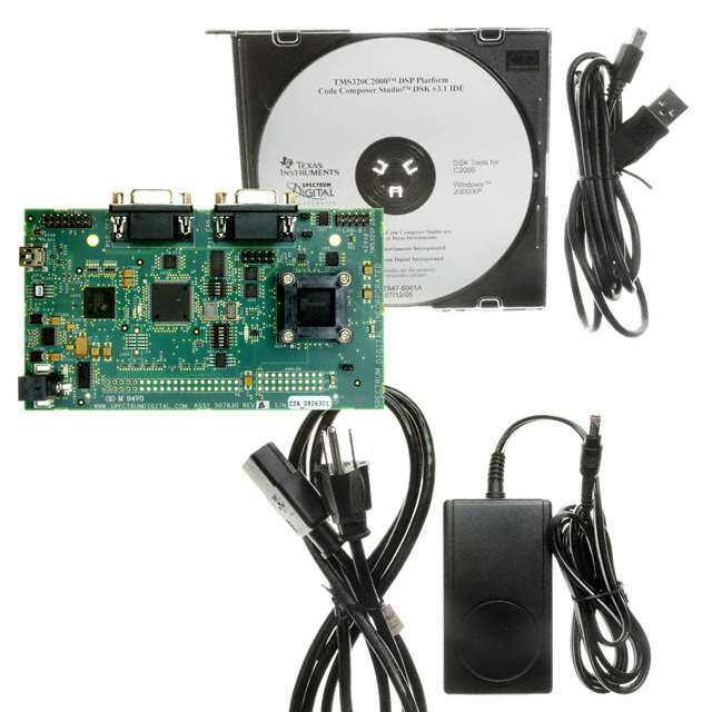
| 描述 | EVAL KIT FOR TMS320F28X开发板和工具包 - TMS320 F28069 Piccolo Experimenter Kit |
| 产品分类 | 评估板 - 嵌入式 - MCU, DSP工程工具 |
| 品牌 | Texas Instruments |
| 产品手册 | |
| 产品图片 |
|
| rohs | 否含铅 / 不受限制有害物质指令(RoHS)规范要求限制 |
| 产品系列 | 嵌入式开发工具,嵌入式处理器开发套件,开发板和工具包 - TMS320,Texas Instruments TMDSDOCK28069C2000™, Piccolo™ |
| 数据手册 | 点击此处下载产品Datasheethttp://www.ti.com/lit/pdf/spruh18点击此处下载产品Datasheet |
| 产品型号 | TMDSDOCK28069 |
| 产品 | Experiment Kits |
| 产品种类 | 开发板和工具包 - TMS320 |
| 其它名称 | 296-36883 |
| 兼容软件 | controlSUITE |
| 内容 | 板,电缆 |
| 商标 | Texas Instruments |
| 安装类型 | 固定 |
| 工作电源电压 | 5 V |
| 工具用于评估 | TMS320F28069 |
| 平台 | 试验套件 |
| 接口类型 | USB |
| 描述/功能 | F28069 Piccolo experimenter kit |
| 操作系统 | - |
| 数据总线宽度 | 32 bit |
| 板类型 | 评估平台 |
| 标准包装 | 1 |
| 核心 | TMS320 |
| 核心处理器 | C28x |
| 用于 | TMDSCNCD28069ISO |
| 类型 | MCU 32-位 |
| 配套使用产品/相关产品 | TMS320F28069 |


- 商务部:美国ITC正式对集成电路等产品启动337调查
- 曝三星4nm工艺存在良率问题 高通将骁龙8 Gen1或转产台积电
- 太阳诱电将投资9.5亿元在常州建新厂生产MLCC 预计2023年完工
- 英特尔发布欧洲新工厂建设计划 深化IDM 2.0 战略
- 台积电先进制程称霸业界 有大客户加持明年业绩稳了
- 达到5530亿美元!SIA预计今年全球半导体销售额将创下新高
- 英特尔拟将自动驾驶子公司Mobileye上市 估值或超500亿美元
- 三星加码芯片和SET,合并消费电子和移动部门,撤换高东真等 CEO
- 三星电子宣布重大人事变动 还合并消费电子和移动部门
- 海关总署:前11个月进口集成电路产品价值2.52万亿元 增长14.8%


PDF Datasheet 数据手册内容提取
TMS320x2806x Technical Reference Manual LiteratureNumber:SPRUH18H January2011–RevisedNovember2019
Contents Preface....................................................................................................................................... 43 1 SystemControlandInterrupts............................................................................................. 45 1.2 FlashandOTPMemoryBlocks.......................................................................................... 46 1.2.1 FlashMemory...................................................................................................... 46 1.2.2 OTPMemory....................................................................................................... 46 1.2.3 FlashandOTPPowerModes................................................................................... 47 1.2.4 FlashandOTPRegisters........................................................................................ 52 1.3 CodeSecurityModule(CSM)............................................................................................. 58 1.3.1 FunctionalDescription............................................................................................ 58 1.3.2 CSMImpactonOtherOn-ChipResources.................................................................... 60 1.3.3 IncorporatingCodeSecurityinUserApplications ............................................................ 60 1.3.4 Do'sandDon'tstoProtectSecurityLogic...................................................................... 66 1.3.5 CSMFeatures-Summary....................................................................................... 66 1.4 Clocking ..................................................................................................................... 67 1.4.1 ClockingandSystemControl.................................................................................... 67 1.4.2 OSCandPLLBlock............................................................................................... 74 1.4.3 Low-PowerModesBlock......................................................................................... 99 1.4.4 CPUWatchdogBlock........................................................................................... 101 1.4.5 32-BitCPUTimers0/1/2........................................................................................ 107 1.5 General-PurposeInput/Output(GPIO)................................................................................. 112 1.5.1 GPIOModuleOverview......................................................................................... 112 1.5.2 ConfigurationOverview......................................................................................... 118 1.5.3 DigitalGeneralPurposeI/OControl........................................................................... 120 1.5.4 InputQualification................................................................................................ 121 1.5.5 GPIOandPeripheralMultiplexing(MUX) .................................................................... 126 1.5.6 RegisterBitDefinitions.......................................................................................... 130 1.6 PeripheralFrames........................................................................................................ 156 1.6.1 PeripheralFrameRegisters.................................................................................... 156 1.6.2 EALLOW-ProtectedRegisters................................................................................. 158 1.6.3 DeviceEmulationRegisters.................................................................................... 162 1.6.4 Write-Followed-by-ReadProtection........................................................................... 165 1.7 PeripheralInterruptExpansion(PIE)................................................................................... 166 1.7.1 OverviewofthePIEController................................................................................. 166 1.7.2 VectorTableMapping........................................................................................... 169 1.7.3 InterruptSources................................................................................................. 171 1.7.4 PIEConfigurationRegisters.................................................................................... 180 1.7.5 PIEInterruptRegisters.......................................................................................... 181 1.7.6 ExternalInterruptControlRegisters .......................................................................... 189 1.8 VREG/BOR/POR......................................................................................................... 191 1.8.1 On-chipVoltageRegulator(VREG)........................................................................... 191 1.8.2 On-chipPower-OnReset(POR)andBrown-OutReset(BOR)Circuit................................... 192 2 BootROM........................................................................................................................ 193 2.1 BootROMMemoryMap................................................................................................. 194 2.1.1 On-ChipBootROMMathTables.............................................................................. 196 2.1.2 On-ChipBootROMIQmathFunctions........................................................................ 198 2 Contents SPRUH18H–January2011–RevisedNovember2019 SubmitDocumentationFeedback Copyright©2011–2019,TexasInstrumentsIncorporated
www.ti.com 2.1.3 On-ChipFlashAPI............................................................................................... 198 2.1.4 CPUVectorTable............................................................................................... 198 2.2 BootloaderFeatures...................................................................................................... 201 2.2.1 BootloaderFunctionalOperation.............................................................................. 201 2.2.2 BootloaderDeviceConfiguration.............................................................................. 202 2.2.3 PLLMultiplierandDIVSELSelection......................................................................... 202 2.2.4 WatchdogModule ............................................................................................... 203 2.2.5 TakinganITRAPInterrupt...................................................................................... 203 2.2.6 InternalPullupResisters........................................................................................ 203 2.2.7 PIEConfiguration................................................................................................ 203 2.2.8 ReservedMemory............................................................................................... 203 2.2.9 BootloaderModes............................................................................................... 205 2.2.10 Device_Cal ...................................................................................................... 211 2.2.11 BootloaderDataStreamStructure........................................................................... 211 2.2.12 BasicTransferProcedure ..................................................................................... 216 2.2.13 InitBootAssemblyRoutine .................................................................................... 217 2.2.14 SelectBootModeFunction .................................................................................... 218 2.2.15 CopyDataFunction............................................................................................. 221 2.2.16 SCI_BootFunction ............................................................................................. 221 2.2.17 Parallel_BootFunction(GPIO)................................................................................ 223 2.2.18 SPI_BootFunction.............................................................................................. 228 2.2.19 I2CBootFunction .............................................................................................. 231 2.2.20 eCANBootFunction ........................................................................................... 234 2.2.21 ExitBootAssemblyRoutine................................................................................... 236 2.3 BuildingtheBootTable.................................................................................................. 237 2.3.1 TheC2000HexUtility........................................................................................... 237 2.3.2 Example:PreparingaCOFFFileForeCANBootloading.................................................. 238 2.4 BootloaderCodeOverview.............................................................................................. 242 2.4.1 BootROMVersionandChecksumInformation ............................................................. 242 3 EnhancedPulseWidthModulator(ePWM)Module................................................................ 243 3.1 Introduction................................................................................................................ 244 3.1.1 SubmoduleOverview............................................................................................ 244 3.1.2 RegisterMapping................................................................................................ 247 3.2 ePWMSubmodules...................................................................................................... 250 3.2.1 Overview.......................................................................................................... 250 3.2.2 Time-Base(TB)Submodule.................................................................................... 252 3.2.3 Counter-Compare(CC)Submodule........................................................................... 261 3.2.4 Action-Qualifier(AQ)Submodule.............................................................................. 267 3.2.5 Dead-BandGenerator(DB)Submodule...................................................................... 282 3.2.6 PWM-Chopper(PC)Submodule............................................................................... 287 3.2.7 Trip-Zone(TZ)Submodule..................................................................................... 291 3.2.8 Event-Trigger(ET)Submodule................................................................................ 296 3.2.9 DigitalCompare(DC)Submodule............................................................................. 301 3.3 ApplicationstoPowerTopologies...................................................................................... 307 3.3.1 OverviewofMultipleModules ................................................................................. 307 3.3.2 KeyConfigurationCapabilities................................................................................. 307 3.3.3 ControllingMultipleBuckConvertersWithIndependentFrequencies.................................... 308 3.3.4 ControllingMultipleBuckConvertersWithSameFrequencies............................................ 312 3.3.5 ControllingMultipleHalfH-Bridge(HHB)Converters....................................................... 315 3.3.6 ControllingDual3-PhaseInvertersforMotors(ACIandPMSM).......................................... 317 3.3.7 PracticalApplicationsUsingPhaseControlBetweenPWMModules.................................... 321 3.3.8 Controllinga3-PhaseInterleavedDC/DCConverter....................................................... 322 3.3.9 ControllingZeroVoltageSwitchedFullBridge(ZVSFB)Converter....................................... 327 SPRUH18H–January2011–RevisedNovember2019 Contents 3 SubmitDocumentationFeedback Copyright©2011–2019,TexasInstrumentsIncorporated
www.ti.com 3.3.10 ControllingaPeakCurrentModeControlledBuckModule............................................... 329 3.3.11 ControllingH-BridgeLLCResonantConverter............................................................. 331 3.4 Registers................................................................................................................... 334 3.4.1 Time-BaseSubmoduleRegisters.............................................................................. 334 3.4.2 Counter-CompareSubmoduleRegisters..................................................................... 341 3.4.3 Action-QualifierSubmoduleRegisters........................................................................ 345 3.4.4 Dead-BandSubmoduleRegisters............................................................................. 348 3.4.5 PWM-ChopperSubmoduleControlRegister................................................................. 351 3.4.6 Trip-ZoneSubmoduleControlandStatusRegisters........................................................ 353 3.4.7 DigitalCompareSubmoduleRegisters....................................................................... 360 3.4.8 Event-TriggerSubmoduleRegisters.......................................................................... 365 3.4.9 ProperInterruptInitializationProcedure...................................................................... 371 4 High-ResolutionPulseWidthModulator(HRPWM)................................................................ 372 4.1 Introduction................................................................................................................ 373 4.2 OperationalDescriptionofHRPWM.................................................................................... 375 4.2.1 ControllingtheHRPWMCapabilities.......................................................................... 376 4.2.2 ConfiguringtheHRPWM........................................................................................ 378 4.2.3 PrincipleofOperation........................................................................................... 379 4.2.4 ScaleFactorOptimizingSoftware(SFO)..................................................................... 389 4.2.5 HRPWMExamplesUsingOptimizedAssemblyCode...................................................... 389 4.3 HRPWMRegisterDescriptions......................................................................................... 395 4.3.1 RegisterSummary............................................................................................... 395 4.3.2 RegistersandFieldDescriptions.............................................................................. 396 4.4 AppendixA:SFOLibrarySoftware-SFO_TI_Build_V6.lib......................................................... 400 4.5 ScaleFactorOptimizerFunction-intSFO().......................................................................... 400 4.6 SoftwareUsage........................................................................................................... 401 4.7 SFOLibraryVersionSoftwareDifferences............................................................................ 402 5 HighResolutionCapture(HRCAP)...................................................................................... 404 5.1 Introduction................................................................................................................ 405 5.2 Description................................................................................................................. 405 5.3 OperationalDetails....................................................................................................... 406 5.3.1 HRCAPClocking................................................................................................. 406 5.3.2 HRCAPModesofOperation................................................................................... 407 5.3.3 HRCAPInterrupts................................................................................................ 410 5.4 RegisterDescriptions..................................................................................................... 411 5.4.1 HRCAPControlRegister(HCCTL)–EALLOWprotected ................................................. 411 5.4.2 HRCAPInterruptFlagRegister(HCIFR)–EALLOWprotected........................................... 412 5.4.3 HRCAPInterruptClearRegister(HCICLR)–EALLOWprotected........................................ 414 5.4.4 HRCAPInterruptForceRegister(HCIFRC)–EALLOWprotected........................................ 415 5.4.5 HRCAPCounterRegister(HCCOUNTER)................................................................... 415 5.4.6 HRCAPCaptureCounterOnRisingEdge0Register(HCCAPCNTRISE0)............................. 416 5.4.7 HRCAPCaptureCounterOnRisingEdge1Register(HCCAPCNTRISE1)............................. 416 5.4.8 HRCAPCaptureCounterOnFallingEdge0Register(HCCAPCNTFALL0)............................ 416 5.4.9 HRCAPCaptureCounterOnFallingEdge1Register(HCCAPCNTFALL1)............................ 417 5.5 HRCAPCalibrationLibrary ............................................................................................. 417 5.5.1 HRCAPCalibrationLibraryFunctions ........................................................................ 418 5.5.2 HRCAPCalibrationLibrarySoftwareUsage................................................................. 422 6 EnhancedCapture(eCAP)................................................................................................. 425 6.1 Introduction................................................................................................................ 426 6.2 Features.................................................................................................................... 426 6.3 Description................................................................................................................. 426 6.4 CaptureandAPWMOperatingMode.................................................................................. 428 6.5 CaptureModeDescription............................................................................................... 429 4 Contents SPRUH18H–January2011–RevisedNovember2019 SubmitDocumentationFeedback Copyright©2011–2019,TexasInstrumentsIncorporated
www.ti.com 6.5.1 EventPrescaler.................................................................................................. 430 6.5.2 EdgePolaritySelectandQualifier............................................................................. 431 6.5.3 Continuous/One-ShotControl.................................................................................. 431 6.5.4 32-BitCounterandPhaseControl............................................................................. 432 6.5.5 CAP1-CAP4Registers.......................................................................................... 433 6.5.6 eCAPSynchronization.......................................................................................... 433 6.5.7 InterruptControl.................................................................................................. 433 6.5.8 ShadowLoadandLockoutControl............................................................................ 435 6.5.9 APWMModeOperation......................................................................................... 435 6.6 ApplicationoftheeCAPModule ....................................................................................... 437 6.6.1 Example1-AbsoluteTime-StampOperationRisingEdgeTrigger....................................... 437 6.6.2 Example2-AbsoluteTime-StampOperationRisingandFallingEdgeTrigger ........................ 438 6.6.3 Example3-TimeDifference(Delta)OperationRisingEdgeTrigger..................................... 439 6.6.4 Example4-TimeDifference(Delta)OperationRisingandFallingEdgeTrigger ...................... 440 6.7 ApplicationoftheAPWMMode......................................................................................... 441 6.7.1 Example1-SimplePWMGeneration(IndependentChannel/s).......................................... 441 6.8 eCAPRegisters........................................................................................................... 442 6.8.1 eCAPBaseAddresses.......................................................................................... 442 6.8.2 ECAP_REGSRegisters......................................................................................... 443 7 EnhancedQuadratureEncoderPulse(eQEP)....................................................................... 460 7.1 Introduction................................................................................................................ 461 7.2 ConfiguringDevicePins................................................................................................. 463 7.3 Description................................................................................................................. 463 7.3.1 EQEPInputs...................................................................................................... 463 7.3.2 FunctionalDescription........................................................................................... 464 7.3.3 eQEPMemoryMap ............................................................................................. 465 7.4 QuadratureDecoderUnit(QDU)....................................................................................... 466 7.4.1 PositionCounterInputModes.................................................................................. 466 7.4.2 eQEPInputPolaritySelection.................................................................................. 469 7.4.3 Position-CompareSyncOutput................................................................................ 469 7.5 PositionCounterandControlUnit(PCCU)............................................................................ 469 7.5.1 PositionCounterOperatingModes............................................................................ 469 7.5.2 PositionCounterLatch.......................................................................................... 471 7.5.3 PositionCounterInitialization.................................................................................. 473 7.5.4 eQEPPosition-compareUnit................................................................................... 474 7.6 eQEPEdgeCaptureUnit................................................................................................ 475 7.7 eQEPWatchdog.......................................................................................................... 479 7.8 UnitTimerBase........................................................................................................... 479 7.9 eQEPInterruptStructure ................................................................................................ 480 7.10 eQEPRegisters........................................................................................................... 481 7.10.1 eQEPBaseAddresses ........................................................................................ 481 7.10.2 EQEP_REGSRegisters....................................................................................... 482 8 Analog-to-DigitalConverter(ADC)...................................................................................... 516 8.1 ADCOverview............................................................................................................. 517 8.2 Features.................................................................................................................... 517 8.3 BlockDiagram............................................................................................................. 517 8.4 SOCPrincipleofOperation.............................................................................................. 518 8.4.1 ADCAcquisition(SampleandHold)Window................................................................ 520 8.4.2 TriggerOperation................................................................................................ 524 8.4.3 ChannelSelection............................................................................................... 525 8.5 ONESHOTSingleConversionSupport................................................................................ 525 8.6 ADCConversionPriority................................................................................................. 526 8.7 SequentialSamplingMode.............................................................................................. 529 SPRUH18H–January2011–RevisedNovember2019 Contents 5 SubmitDocumentationFeedback Copyright©2011–2019,TexasInstrumentsIncorporated
www.ti.com 8.8 SimultaneousSamplingMode.......................................................................................... 529 8.9 EOCandInterruptOperation............................................................................................ 530 8.10 Power-UpSequence..................................................................................................... 530 8.11 ADCCalibration........................................................................................................... 531 8.11.1 FactorySettingsandCalibrationFunction .................................................................. 531 8.11.2 ADCZeroOffsetCalibration .................................................................................. 531 8.11.3 ADCFullScaleGainCalibration.............................................................................. 532 8.11.4 ADCBiasCurrentCalibration................................................................................. 532 8.12 Internal/ExternalReferenceVoltageSelection........................................................................ 532 8.12.1 InternalReferenceVoltage.................................................................................... 532 8.12.2 ExternalReferenceVoltage................................................................................... 532 8.13 ADCRegisters............................................................................................................ 534 8.13.1 ADCControlRegister1(ADCCTL1) ........................................................................ 534 8.13.2 ADCControlRegister2(ADCCTL2)......................................................................... 536 8.13.3 ADCInterruptRegisters ....................................................................................... 537 8.13.4 ADCPriorityRegister .......................................................................................... 541 8.13.5 ADCSOCRegisters............................................................................................ 543 8.13.6 ADCCalibrationRegisters..................................................................................... 549 8.13.7 ComparatorHysteresisControlRegister.................................................................... 550 8.13.8 ADCRevisionRegister ........................................................................................ 550 8.13.9 ADCResultRegisters.......................................................................................... 550 8.14 ADCTimings.............................................................................................................. 551 8.15 InternalTemperatureSensor............................................................................................ 555 8.15.1 TransferFunction............................................................................................... 555 9 Comparator...................................................................................................................... 557 9.1 Introduction................................................................................................................ 558 9.2 Features.................................................................................................................... 558 9.3 BlockDiagram............................................................................................................. 558 9.4 ComparatorFunction..................................................................................................... 558 9.5 DACReference........................................................................................................... 559 9.6 RampGeneratorInput................................................................................................... 559 9.7 Initialization................................................................................................................ 561 9.8 DigitalDomainManipulation............................................................................................. 561 9.9 ComparatorRegisters.................................................................................................... 562 9.9.1 ComparatorControl(COMPCTL)Register .................................................................. 562 9.9.2 CompareOutputStatus(COMPSTS)Register.............................................................. 563 9.9.3 DACControl(DACCTL)Register ............................................................................. 563 9.9.4 DACValue(DACVAL)Register................................................................................ 564 9.9.5 RampGeneratorMaximumReferenceActive(RAMPMAXREF_ACTIVE)Register ................... 564 9.9.6 RampGeneratorMaximumReferenceShadow(RAMPMAXREF_SHDW)Register................... 565 9.9.7 RampGeneratorDecrementValueActive(RAMPDECVAL_ACTIVE)Register........................ 565 9.9.8 RampGeneratorDecrementValueShadow(RAMPDECVAL_SHDW)Register....................... 565 9.9.9 RampGeneratorStatus(RAMPSTS)Register.............................................................. 565 10 ControlLawAccelerator(CLA)........................................................................................... 567 10.1 Introduction................................................................................................................ 568 10.2 Features.................................................................................................................... 568 10.3 CLAInterface.............................................................................................................. 570 10.3.1 CLAMemory.................................................................................................... 570 10.3.2 CLAMemoryBus............................................................................................... 570 10.3.3 SharedPeripheralsandEALLOWProtection............................................................... 571 10.3.4 CLATasksandInterruptVectors............................................................................. 572 10.4 CLAandCPUArbitration................................................................................................ 573 10.4.1 CLAandCPUArbitration...................................................................................... 573 6 Contents SPRUH18H–January2011–RevisedNovember2019 SubmitDocumentationFeedback Copyright©2011–2019,TexasInstrumentsIncorporated
www.ti.com 10.5 CLAConfigurationandDebug.......................................................................................... 578 10.5.1 BuildingaCLAApplication.................................................................................... 578 10.5.2 TypicalCLAInitializationSequence.......................................................................... 578 10.5.3 DebuggingCLACode.......................................................................................... 579 10.5.4 CLAIllegalOpcodeBehavior................................................................................. 580 10.5.5 ResettingtheCLA.............................................................................................. 580 10.6 Pipeline..................................................................................................................... 582 10.6.1 PipelineOverview............................................................................................... 582 10.6.2 CLAPipelineAlignment........................................................................................ 582 10.6.3 ParallelInstructions............................................................................................. 586 10.7 InstructionSet............................................................................................................. 587 10.7.1 InstructionDescriptions........................................................................................ 587 10.7.2 AddressingModesandEncoding............................................................................ 589 10.7.3 Instructions...................................................................................................... 591 10.8 RegisterSet............................................................................................................... 702 10.8.1 RegisterMemoryMapping .................................................................................... 702 10.8.2 TaskInterruptVectorRegisters............................................................................... 703 10.8.3 ConfigurationRegisters........................................................................................ 704 10.8.4 ExecutionRegisters............................................................................................ 716 11 DirectMemoryAccess(DMA)Module ................................................................................ 719 11.1 Introduction ............................................................................................................... 720 11.2 DMAOverview............................................................................................................ 720 11.3 Architecture................................................................................................................ 720 11.3.1 BlockDiagram................................................................................................... 720 11.3.2 PeripheralInterruptEventTriggerSources................................................................. 721 11.3.3 DMABus......................................................................................................... 723 11.4 PipelineTimingandThroughput........................................................................................ 724 11.5 CPUArbitration ........................................................................................................... 725 11.6 ChannelPriority........................................................................................................... 725 11.6.1 Round-RobinMode............................................................................................. 725 11.6.2 Channel1HighPriorityMode................................................................................. 726 11.7 AddressPointerandTransferControl................................................................................. 726 11.8 OverrunDetectionFeature.............................................................................................. 731 11.9 RegisterDescriptions..................................................................................................... 733 11.9.1 DMAControlRegister(DMACTRL)—EALLOWProtected.............................................. 734 11.9.2 DebugControlRegister(DEBUGCTRL)—EALLOWProtected......................................... 736 11.9.3 RevisionRegister(REVISION) ............................................................................... 736 11.9.4 PriorityControlRegister1(PRIORITYCTRL1)—EALLOWProtected................................. 737 11.9.5 PriorityStatusRegister(PRIORITYSTAT).................................................................. 738 11.9.6 ModeRegister(MODE)—EALLOWProtected............................................................ 739 11.9.7 ControlRegister(CONTROL)—EALLOWProtected..................................................... 741 11.9.8 BurstSizeRegister(BURST_SIZE)—EALLOWProtected.............................................. 743 11.9.9 BURST_COUNTRegister..................................................................................... 743 11.9.10 SourceBurstStepRegisterSize(SRC_BURST_STEP)—EALLOWProtected.................... 744 11.9.11 DestinationBurstStepRegisterSize(DST_BURST_STEP)—EALLOWProtected................ 745 11.9.12 TransferSizeRegister(TRANSFER_SIZE)—EALLOWProtected................................... 745 11.9.13 TransferCountRegister(TRANSFER_COUNT) ......................................................... 746 11.9.14 SourceTransferStepSizeRegister(SRC_TRANSFER_STEP)—EALLOWProtected........... 746 11.9.15 DestinationTransferStepSizeRegister(DST_TRANSFER_STEP)—EALLOWProtected....... 747 11.9.16 Source/DestinationWrapSizeRegister(SRC/DST_WRAP_SIZE)—EALLOWprotected)........ 747 11.9.17 Source/DestinationWrapCountRegister(SCR/DST_WRAP_COUNT) .............................. 748 11.9.18 Source/DestinationWrapStepSizeRegisters(SRC/DST_WRAP_STEP)—EALLOWProtected 748 11.9.19 ShadowSourceBeginandCurrentAddressPointerRegisters SPRUH18H–January2011–RevisedNovember2019 Contents 7 SubmitDocumentationFeedback Copyright©2011–2019,TexasInstrumentsIncorporated
www.ti.com (SRC_BEG_ADDR_SHADOW/DST_BEG_ADDR_SHADOW)—AllEALLOWProtected............ 749 11.9.20 ActiveSourceBeginandCurrentAddressPointerRegisters (SRC_BEG_ADDR/DST_BEG_ADDR)....................................................................... 749 11.9.21 ShadowDestinationBeginandCurrentAddressPointerRegisters (SRC_ADDR_SHADOW/DST_ADDR_SHADOW)—AllEALLOWProtected.......................... 750 11.9.22 ActiveDestinationBeginandCurrentAddressPointerRegisters(SRC_ADDR/DST_ADDR)..... 750 12 SerialPeripheralInterface(SPI).......................................................................................... 751 12.1 Introduction................................................................................................................ 752 12.1.1 Features.......................................................................................................... 752 12.1.2 BlockDiagram.................................................................................................. 752 12.2 System-LevelIntegration................................................................................................ 753 12.2.1 SPIModuleSignals............................................................................................. 753 12.2.2 ConfiguringDevicePins....................................................................................... 754 12.2.3 SPIInterrupts.................................................................................................... 754 12.3 SPIOperation............................................................................................................. 756 12.3.1 IntroductiontoOperation...................................................................................... 756 12.3.2 MasterMode.................................................................................................... 757 12.3.3 SlaveMode...................................................................................................... 758 12.3.4 DataFormat..................................................................................................... 758 12.3.5 BaudRateSelection ........................................................................................... 759 12.3.6 SPIClockingSchemes......................................................................................... 760 12.3.7 SPIFIFODescription........................................................................................... 761 12.3.8 SPI3-WireModeDescription................................................................................. 762 12.4 ProgrammingProcedure................................................................................................. 764 12.4.1 InitializationUponReset....................................................................................... 764 12.4.2 ConfiguringtheSPI............................................................................................. 764 12.4.3 DataTransferExample........................................................................................ 764 12.4.4 SPI3-WireModeCodeExamples............................................................................ 766 12.4.5 SPISTEINVBitinDigitalAudioTransfers.................................................................. 767 12.5 SPIRegisters.............................................................................................................. 769 12.5.1 SPIBaseAddresses........................................................................................... 769 12.5.2 SPI_REGSRegisters .......................................................................................... 770 13 SerialCommunicationsInterface(SCI)................................................................................ 789 13.1 Introduction................................................................................................................ 790 13.2 Architecture................................................................................................................ 792 13.3 SCIModuleSignalSummary ........................................................................................... 792 13.4 ConfiguringDevicePins................................................................................................. 792 13.5 MultiprocessorandAsynchronousCommunicationModes......................................................... 792 13.6 SCIProgrammableDataFormat ....................................................................................... 793 13.7 SCIMultiprocessorCommunication.................................................................................... 793 13.7.1 RecognizingtheAddressByte................................................................................ 794 13.7.2 ControllingtheSCITXandRXFeatures.................................................................... 794 13.7.3 ReceiptSequence.............................................................................................. 794 13.8 Idle-LineMultiprocessorMode.......................................................................................... 794 13.8.1 Idle-LineModeSteps........................................................................................... 795 13.8.2 BlockStartSignal............................................................................................... 796 13.8.3 Wake-UPTemporary(WUT)Flag............................................................................ 796 13.8.4 ReceiverOperation............................................................................................. 796 13.9 Address-BitMultiprocessorMode ...................................................................................... 796 13.9.1 SendinganAddress............................................................................................ 796 13.10 SCICommunicationFormat............................................................................................. 797 13.10.1 ReceiverSignalsinCommunicationModes............................................................... 798 13.10.2 TransmitterSignalsinCommunicationModes............................................................ 798 8 Contents SPRUH18H–January2011–RevisedNovember2019 SubmitDocumentationFeedback Copyright©2011–2019,TexasInstrumentsIncorporated
www.ti.com 13.11 SCIPortInterrupts ....................................................................................................... 799 13.12 SCIBaudRateCalculations............................................................................................ 800 13.13 SCIEnhancedFeatures................................................................................................. 800 13.13.1 SCIFIFODescription......................................................................................... 800 13.13.2 SCIAuto-Baud................................................................................................. 802 13.13.3 Autobaud-DetectSequence ................................................................................. 802 13.14 SCIRegisters............................................................................................................. 803 13.14.1 SCIBaseAddresses.......................................................................................... 803 13.14.2 SCI_REGSRegisters......................................................................................... 804 14 Inter-IntegratedCircuitModule(I2C) ................................................................................... 824 14.1 Introduction................................................................................................................ 825 14.1.1 Features.......................................................................................................... 825 14.1.2 FeaturesNotSupported....................................................................................... 826 14.1.3 FunctionalOverview............................................................................................ 826 14.1.4 ClockGeneration............................................................................................... 827 14.1.5 I2CClockDividerRegisters(I2CCLKLandI2CCLKH).................................................... 828 14.2 ConfiguringDevicePins................................................................................................. 828 14.3 I2CModuleOperationalDetails......................................................................................... 829 14.3.1 InputandOutputVoltageLevels............................................................................. 829 14.3.2 DataValidity..................................................................................................... 829 14.3.3 OperatingModes ............................................................................................... 829 14.3.4 I2CModuleSTARTandSTOPConditions.................................................................. 830 14.3.5 SerialDataFormats............................................................................................ 831 14.3.6 NACKBitGeneration........................................................................................... 833 14.3.7 ClockSynchronization ......................................................................................... 834 14.3.8 Arbitration........................................................................................................ 834 14.3.9 DigitalLoopbackMode......................................................................................... 835 14.4 InterruptRequestsGeneratedbytheI2CModule.................................................................... 836 14.4.1 BasicI2CInterruptRequests.................................................................................. 836 14.4.2 I2CFIFOInterrupts............................................................................................. 838 14.5 ResettingorDisablingtheI2CModule................................................................................. 839 14.6 I2CRegisters.............................................................................................................. 840 14.6.1 I2CBaseAddresses ........................................................................................... 840 14.6.2 I2C_REGSRegisters........................................................................................... 841 15 MultichannelBufferedSerialPort(McBSP).......................................................................... 865 15.1 Overview................................................................................................................... 866 15.1.1 FeaturesoftheMcBSP........................................................................................ 866 15.1.2 McBSPPins/Signals............................................................................................ 867 15.1.3 McBSPOperation............................................................................................... 868 15.1.4 DataTransferProcessofMcBSP............................................................................ 869 15.1.5 Companding(CompressingandExpanding)Data......................................................... 869 15.2 ClockingandFramingData ............................................................................................. 871 15.2.1 Clocking.......................................................................................................... 871 15.2.2 SerialWords..................................................................................................... 871 15.2.3 FramesandFrameSynchronization......................................................................... 872 15.2.4 GeneratingTransmitandReceiveInterrupts ............................................................... 872 15.2.5 IgnoringFrame-SynchronizationPulses..................................................................... 872 15.2.6 FrameFrequency............................................................................................... 873 15.2.7 MaximumFrameFrequency.................................................................................. 873 15.3 FramePhases............................................................................................................. 873 15.3.1 NumberofPhases,Words,andBitsPerFrame........................................................... 874 15.3.2 Single-PhaseFrameExample................................................................................ 874 15.3.3 Dual-PhaseFrameExample.................................................................................. 874 SPRUH18H–January2011–RevisedNovember2019 Contents 9 SubmitDocumentationFeedback Copyright©2011–2019,TexasInstrumentsIncorporated
www.ti.com 15.3.4 ImplementingtheAC97StandardWithaDual-PhaseFrame............................................ 875 15.3.5 McBSPReception.............................................................................................. 875 15.3.6 McBSPTransmission.......................................................................................... 877 15.3.7 InterruptsandDMAEventsGeneratedbyaMcBSP...................................................... 878 15.4 McBSPSampleRateGenerator........................................................................................ 878 15.4.1 BlockDiagram................................................................................................... 879 15.4.2 FrameSynchronizationGenerationintheSampleRateGenerator..................................... 882 15.4.3 SynchronizingSampleRateGeneratorOutputstoanExternalClock .................................. 882 15.4.4 ResetandInitializationProcedurefortheSampleRateGenerator...................................... 884 15.5 McBSPException/ErrorConditions.................................................................................... 885 15.5.1 TypesofErrors.................................................................................................. 885 15.5.2 OverrunintheReceiver........................................................................................ 885 15.5.3 UnexpectedReceiveFrame-SynchronizationPulse....................................................... 887 15.5.4 OverwriteintheTransmitter................................................................................... 889 15.5.5 UnexpectedTransmitFrame-SynchronizationPulse...................................................... 891 15.6 MultichannelSelectionModes.......................................................................................... 893 15.6.1 Channels,Blocks,andPartitions............................................................................. 893 15.6.2 MultichannelSelection......................................................................................... 894 15.6.3 ConfiguringaFrameforMultichannelSelection............................................................ 894 15.6.4 UsingTwoPartitions........................................................................................... 894 15.6.5 UsingEightPartitions.......................................................................................... 896 15.6.6 ReceiveMultichannelSelectionMode....................................................................... 897 15.6.7 TransmitMultichannelSelectionModes..................................................................... 897 15.7 SPIOperationUsingtheClockStopMode............................................................................ 900 15.7.1 SPIProtocol..................................................................................................... 900 15.7.2 ClockStopMode................................................................................................ 901 15.7.3 BitsUsedtoEnableandConfiguretheClockStopMode ................................................ 901 15.7.4 ClockStopModeTimingDiagrams.......................................................................... 902 15.7.5 ProcedureforConfiguringaMcBSPforSPIOperation................................................... 904 15.7.6 McBSPastheSPIMaster..................................................................................... 904 15.7.7 McBSPasanSPISlave....................................................................................... 906 15.8 ReceiverConfiguration................................................................................................... 907 15.8.1 ProgrammingtheMcBSPRegistersfortheDesiredReceiverOperation............................... 907 15.8.2 ResettingandEnablingtheReceiver........................................................................ 908 15.8.3 SettheReceiverPinstoOperateasMcBSPPins......................................................... 908 15.8.4 Enable/DisabletheDigitalLoopbackMode................................................................. 909 15.8.5 Enable/DisabletheClockStopMode........................................................................ 909 15.8.6 Enable/DisabletheReceiveMultichannelSelectionMode................................................ 910 15.8.7 ChooseOneorTwoPhasesfortheReceiveFrame...................................................... 910 15.8.8 SettheReceiveWordLength(s).............................................................................. 911 15.8.9 SettheReceiveFrameLength............................................................................... 911 15.8.10 Enable/DisabletheReceiveFrame-SynchronizationIgnoreFunction................................. 912 15.8.11 SettheReceiveCompandingMode........................................................................ 913 15.8.12 SettheReceiveDataDelay................................................................................. 914 15.8.13 SettheReceiveSign-ExtensionandJustificationMode................................................. 916 15.8.14 SettheReceiveInterruptMode............................................................................. 917 15.8.15 SettheReceiveFrame-SynchronizationMode........................................................... 917 15.8.16 SettheReceiveFrame-SynchronizationPolarity......................................................... 919 15.8.17 SettheReceiveClockMode ................................................................................ 921 15.8.18 SettheReceiveClockPolarity.............................................................................. 922 15.8.19 SettheSRGClockDivide-DownValue.................................................................... 924 15.8.20 SettheSRGClockSynchronizationMode................................................................ 924 15.8.21 SettheSRGClockMode(ChooseanInputClock)...................................................... 924 10 Contents SPRUH18H–January2011–RevisedNovember2019 SubmitDocumentationFeedback Copyright©2011–2019,TexasInstrumentsIncorporated
www.ti.com 15.8.22 SettheSRGInputClockPolarity........................................................................... 926 15.9 TransmitterConfiguration................................................................................................ 926 15.9.1 ProgrammingtheMcBSPRegistersfortheDesiredTransmitterOperation............................ 926 15.9.2 ResettingandEnablingtheTransmitter..................................................................... 927 15.9.3 SettheTransmitterPinstoOperateasMcBSPPins...................................................... 928 15.9.4 Enable/DisabletheDigitalLoopbackMode................................................................. 928 15.9.5 Enable/DisabletheClockStopMode........................................................................ 928 15.9.6 Enable/DisableTransmitMultichannelSelection........................................................... 929 15.9.7 ChooseOneorTwoPhasesfortheTransmitFrame...................................................... 931 15.9.8 SettheTransmitWordLength(s)............................................................................. 931 15.9.9 SettheTransmitFrameLength............................................................................... 932 15.9.10 Enable/DisabletheTransmitFrame-SynchronizationIgnoreFunction................................ 933 15.9.11 SettheTransmitCompandingMode....................................................................... 934 15.9.12 SettheTransmitDataDelay................................................................................. 935 15.9.13 SettheTransmitDXENAMode............................................................................. 937 15.9.14 SettheTransmitInterruptMode............................................................................ 937 15.9.15 SettheTransmitFrame-SynchronizationMode........................................................... 938 15.9.16 SettheTransmitFrame-SynchronizationPolarity........................................................ 939 15.9.17 SettheSRGFrame-SynchronizationPeriodandPulseWidth.......................................... 940 15.9.18 SettheTransmitClockMode................................................................................ 941 15.9.19 SettheTransmitClockPolarity ............................................................................. 941 15.10 EmulationandResetConsiderations.................................................................................. 943 15.10.1 McBSPEmulationMode..................................................................................... 943 15.10.2 ResettingandInitializingMcBSP............................................................................ 943 15.11 DataPackingExamples................................................................................................. 945 15.11.1 DataPackingUsingFrameLengthandWordLength.................................................... 945 15.11.2 DataPackingUsingWordLengthandtheFrame-SynchronizationIgnoreFunction................ 947 15.12 McBSPRegisters......................................................................................................... 947 15.12.1 RegisterSummary............................................................................................ 947 15.12.2 DataReceiveRegisters(DRR[1,2])......................................................................... 948 15.12.3 DataTransmitRegisters(DXR[1,2])........................................................................ 949 15.12.4 SerialPortControlRegisters(SPCR[1,2])................................................................. 950 15.12.5 ReceiveControlRegisters(RCR[1,2]) .................................................................... 955 15.12.6 TransmitControlRegisters(XCR1andXCR2)........................................................... 957 15.12.7 SampleRateGeneratorRegisters(SRGR1andSRGR2)............................................... 960 15.12.8 MultichannelControlRegisters(MCR[1,2])................................................................ 962 15.12.9 PinControlRegister(PCR).................................................................................. 967 15.12.10 ReceiveChannelEnableRegisters(RCERA,RCERB,RCERC,RCERD,RCERE,RCERF, RCERG,RCERH) ............................................................................................... 969 15.12.11 TransmitChannelEnableRegisters(XCERA,XCERB,XCERC,XCERD,XCERE,XCERF, XCERG,XCERH)................................................................................................ 971 15.12.12 InterruptGeneration......................................................................................... 973 16 ControllerAreaNetwork(CAN)........................................................................................... 977 16.1 CANOverview............................................................................................................. 978 16.1.1 Features.......................................................................................................... 978 16.1.2 BlockDiagram................................................................................................... 978 16.2 eCANCompatibilityWithOtherTICANModules.................................................................... 979 16.3 TheCANNetworkandModule ......................................................................................... 979 16.3.1 CANProtocolOverview........................................................................................ 980 16.4 eCANControllerOverview............................................................................................... 981 16.4.1 StandardCANController(SCC)Mode...................................................................... 982 16.4.2 MemoryMap.................................................................................................... 983 16.5 MessageObjects......................................................................................................... 985 16.6 MessageMailbox......................................................................................................... 985 SPRUH18H–January2011–RevisedNovember2019 Contents 11 SubmitDocumentationFeedback Copyright©2011–2019,TexasInstrumentsIncorporated
www.ti.com 16.6.1 TransmitMailbox................................................................................................ 987 16.6.2 ReceiveMailbox................................................................................................ 988 16.6.3 CANModuleOperationinNormalConfiguration........................................................... 988 16.7 eCANConfiguration...................................................................................................... 989 16.7.1 CANModuleInitialization...................................................................................... 989 16.7.2 StepstoConfigureeCAN...................................................................................... 992 16.7.3 HandlingofRemoteFrameMailboxes....................................................................... 994 16.7.4 Interrupts......................................................................................................... 995 16.7.5 CANPower-DownMode..................................................................................... 1000 16.8 eCANRegisters......................................................................................................... 1001 16.8.1 MailboxEnableRegister(CANME)......................................................................... 1001 16.8.2 Mailbox-DirectionRegister(CANMD)....................................................................... 1002 16.8.3 Transmission-RequestSetRegister(CANTRS).......................................................... 1003 16.8.4 Transmission-Request-ResetRegister(CANTRR)....................................................... 1004 16.8.5 Transmission-AcknowledgeRegister(CANTA)........................................................... 1005 16.8.6 Abort-AcknowledgeRegister(CANAA)..................................................................... 1006 16.8.7 Received-Message-PendingRegister(CANRMP)........................................................ 1007 16.8.8 Received-Message-LostRegister(CANRML)............................................................. 1008 16.8.9 Remote-Frame-PendingRegister(CANRFP)............................................................. 1009 16.8.10 GlobalAcceptanceMaskRegister(CANGAM).......................................................... 1011 16.8.11 MasterControlRegister(CANMC)........................................................................ 1012 16.8.12 Bit-TimingConfigurationRegister(CANBTC)............................................................ 1015 16.8.13 ErrorandStatusRegister(CANES)....................................................................... 1017 16.8.14 CANErrorCounterRegisters(CANTEC/CANREC).................................................... 1019 16.8.15 InterruptRegisters........................................................................................... 1020 16.8.16 OverwriteProtectionControlRegister(CANOPC)...................................................... 1027 16.8.17 eCANI/OControlRegisters(CANTIOC,CANRIOC)................................................... 1028 16.8.18 TimerManagementUnit.................................................................................... 1030 16.8.19 MailboxLayout............................................................................................... 1036 16.9 MessageDataRegisters(CANMDL,CANMDH).................................................................... 1039 16.10 AcceptanceFilter........................................................................................................ 1040 16.10.1 Local-AcceptanceMasks(CANLAM)..................................................................... 1040 17 UniversalSerialBus(USB)Controller................................................................................ 1042 17.1 Introduction............................................................................................................... 1043 17.2 Features.................................................................................................................. 1043 17.2.1 BlockDiagram................................................................................................. 1043 17.2.2 SignalDescription............................................................................................. 1044 17.2.3 SignalPinoutTables ......................................................................................... 1044 17.2.4 VBusRecommendations..................................................................................... 1044 17.3 FunctionalDescription.................................................................................................. 1045 17.3.1 OperationasaDevice........................................................................................ 1045 17.3.2 OperationasaHost........................................................................................... 1049 17.3.3 DMAOperation................................................................................................ 1052 17.3.4 Address/DataBusBridge.................................................................................... 1053 17.4 InitializationandConfiguration......................................................................................... 1054 17.4.1 PinConfiguration.............................................................................................. 1054 17.4.2 EndpointConfiguration....................................................................................... 1055 17.5 USBRegisters........................................................................................................... 1056 17.5.1 RegisterMap................................................................................................... 1056 17.5.2 RegisterDescriptions......................................................................................... 1061 RevisionHistory...................................................................................................................... 1125 12 Contents SPRUH18H–January2011–RevisedNovember2019 SubmitDocumentationFeedback Copyright©2011–2019,TexasInstrumentsIncorporated
www.ti.com List of Figures 1-1. FlashPowerModeStateDiagram....................................................................................... 48 1-2. FlashPipeline............................................................................................................... 50 1-3. FlashConfigurationAccessFlowDiagram............................................................................. 51 1-4. FlashOptionsRegister(FOPT).......................................................................................... 53 1-5. FlashPowerRegister(FPWR)........................................................................................... 53 1-6. FlashStatusRegister(FSTATUS)....................................................................................... 54 1-7. FlashStandbyWaitRegister(FSTDBYWAIT) ......................................................................... 55 1-8. FlashStandbytoActiveWaitCounterRegister(FACTIVEWAIT) .................................................. 55 1-9. FlashWait-StateRegister(FBANKWAIT) .............................................................................. 56 1-10. OTPWait-StateRegister(FOTPWAIT) ................................................................................. 57 1-11. CSMStatusandControlRegister(CSMSCR)......................................................................... 62 1-12. PasswordMatchFlow(PMF) ............................................................................................ 63 1-13. ClockandResetDomains ................................................................................................ 68 1-14. PeripheralClockControl0Register(PCLKCR0)...................................................................... 69 1-15. PeripheralClockControl1Register(PCLKCR1)...................................................................... 71 1-16. PeripheralClockControl2Register(PCLKCR2) ..................................................................... 72 1-17. PeripheralClockControl3Register(PCLKCR3)...................................................................... 73 1-18. Low-SpeedPeripheralClockPrescalerRegister(LOSPCP)......................................................... 74 1-19. ClockingOptions........................................................................................................... 75 1-20. InternalOscillatorTrim(INTOSCnTRIM)Register .................................................................... 76 1-21. Clocking(XCLK)Register................................................................................................. 77 1-22. ClockControl(CLKCTL)Register ....................................................................................... 77 1-23. OSCandPLLBlock........................................................................................................ 80 1-24. PLLCRChangeProcedureFlowChart.................................................................................. 82 1-25. PLLCRRegisterLayout................................................................................................... 83 1-26. PLLStatusRegister(PLLSTS)........................................................................................... 83 1-27. PLLLockPeriod(PLLLOCKPRD)Register............................................................................. 85 1-28. PLL2InputandOutputConfigurations.................................................................................. 86 1-29. PLL2Configuration(PLL2CTL)Register(EALLOWprotected)...................................................... 86 1-30. PLL2Multiplier(PLL2MULT)Register(EALLOWprotected)......................................................... 86 1-31. PLL2LockStatus(PLL2STS)Register ................................................................................. 87 1-32. SYSCLK2ClockCounter(SYSCLK2CNTR)Register................................................................. 87 1-33. EPWMDMA/CLAConfiguration(EPWMCFG)Register.............................................................. 88 1-34. ClockingandResetLogic................................................................................................. 89 1-35. ClockFailInterrupt......................................................................................................... 93 1-36. NMIConfiguration(NMICFG)Register.................................................................................. 94 1-37. NMIFlag(NMIFLG)RegisterRegister ................................................................................. 94 1-38. NMIFlag(NMIFLGCLR)RegisterRegister ............................................................................ 95 1-39. NMIFlag(NMIFLGFRC)RegisterRegister ............................................................................ 96 1-40. NMIWatchdogCounter(NMIWDCNT)Register....................................................................... 96 1-41. NMIWatchdogPeriod(NMIWDPRD)Register......................................................................... 96 1-42. XCLKOUTGeneration..................................................................................................... 98 1-43. Low-PowerModeControl0Register(LPMCR0)..................................................................... 100 1-44. CPUWatchdogModule.................................................................................................. 101 1-45. SystemControlandStatusRegister(SCSR) ........................................................................ 104 1-46. WatchdogCounterRegister(WDCNTR).............................................................................. 105 1-47. WatchdogResetKeyRegister(WDKEY) ............................................................................. 105 SPRUH18H–January2011–RevisedNovember2019 ListofFigures 13 SubmitDocumentationFeedback Copyright©2011–2019,TexasInstrumentsIncorporated
www.ti.com 1-48. WatchdogControlRegister(WDCR)................................................................................... 105 1-49. CPU-Timers ............................................................................................................... 107 1-50. CPU-TimerInterruptsSignalsandOutputSignal.................................................................... 107 1-51. TIMERxTIMRegister(x=0,1,2)...................................................................................... 108 1-52. TIMERxTIMHRegister(x=0,1,2).................................................................................... 108 1-53. TIMERxPRDRegister(x=0,1,2)..................................................................................... 109 1-54. TIMERxPRDHRegister(x=0,1,2)................................................................................... 109 1-55. TIMERxTCRRegister(x=0,1,2)..................................................................................... 109 1-56. TIMERxTPRRegister(x=0,1,2)...................................................................................... 110 1-57. TIMERxTPRHRegister(x=0,1,2) ................................................................................... 111 1-58. GeneralGPIOMultiplexingDiagram................................................................................... 113 1-59. GPIO32,GPIO33MultiplexingDiagram............................................................................... 114 1-60. JTAGPort/GPIOMultiplexing........................................................................................... 115 1-61. JTAGDEBUGRegister(Addfress0x702A,EALLOWprotected)................................................... 115 1-62. Analog/GPIOMultiplexing............................................................................................... 117 1-63. InputQualificationUsingaSamplingWindow........................................................................ 122 1-64. InputQualifierClockCycles............................................................................................. 125 1-65. GPIOPortAMUX1(GPAMUX1)Register........................................................................... 130 1-66. GPIOPortAMUX2(GPAMUX2)Register........................................................................... 132 1-67. GPIOPortBMUX1(GPBMUX1)Register........................................................................... 134 1-68. GPIOPortBMUX2(GPBMUX2)Register........................................................................... 136 1-69. AnalogI/OMUX(AIOMUX1)Register................................................................................. 137 1-70. GPIOPortAQualificationControl(GPACTRL)Register ........................................................... 138 1-71. GPIOPortBQualificationControl(GPBCTRL)Register ........................................................... 140 1-72. GPIOAControlRegister2Register(GPACTRL2)Register........................................................ 140 1-73. GPIOPortAQualificationSelect1(GPAQSEL1)Register......................................................... 142 1-74. GPIOPortAQualificationSelect2(GPAQSEL2)Register......................................................... 143 1-75. GPIOPortBQualificationSelect1(GPBQSEL1)Register......................................................... 144 1-76. GPIOPortBQualificationSelect2(GPBQSEL2)Register......................................................... 145 1-77. GPIOPortADirection(GPADIR)Register ........................................................................... 145 1-78. GPIOPortBDirection(GPBDIR)Register ........................................................................... 146 1-79. AnalogI/ODIR(AIODIR)Register..................................................................................... 147 1-80. GPIOPortAPullupDisable(GPAPUD)Registers .................................................................. 147 1-81. GPIOPortBPullupDisable(GPBPUD)Registers .................................................................. 148 1-82. GPIOPortAData(GPADAT)Register ............................................................................... 149 1-83. GPIOPortBData(GPBDAT)Register ............................................................................... 150 1-84. AnalogI/ODAT(AIODAT)Register.................................................................................... 150 1-85. GPIOPortASet,ClearandToggle(GPASET,GPACLEAR,GPATOGGLE)Registers ....................... 151 1-86. GPIOPortBSet,ClearandToggle(GPBSET,GPBCLEAR,GPBTOGGLE)Registers ....................... 152 1-87. AnalogI/OToggle(AIOSET,AIOCLEAR,AIOTOGGLE)Register................................................ 153 1-88. GPIOXINTnInterruptSelect(GPIOXINTnSEL)Registers.......................................................... 154 1-89. GPIOLowPowerModeWakeupSelect(GPIOLPMSEL)Register................................................ 155 1-90. DeviceConfiguration(DEVICECNF)Register........................................................................ 162 1-91. PartIDRegister........................................................................................................... 163 1-92. REVIDRegister........................................................................................................... 164 1-93. Overview:MultiplexingofInterruptsUsingthePIEBlock........................................................... 166 1-94. TypicalPIE/CPUInterruptResponse-INTx.y........................................................................ 168 1-95. ResetFlowDiagram...................................................................................................... 170 1-96. PIEInterruptSourcesandExternalInterruptsXINT1/XINT2/XINT3............................................... 171 14 ListofFigures SPRUH18H–January2011–RevisedNovember2019 SubmitDocumentationFeedback Copyright©2011–2019,TexasInstrumentsIncorporated
www.ti.com 1-97. MultiplexedInterruptRequestFlowDiagram......................................................................... 174 1-98. PIECTRLRegister(Address0xCE0)................................................................................... 181 1-99. PIEInterruptAcknowledgeRegister(PIEACK)Register(Address0xCE1)....................................... 181 1-100. PIEIFRxRegister(x=1to12).......................................................................................... 182 1-101. PIEIERxRegister(x=1to12).......................................................................................... 182 1-102. InterruptFlagRegister(IFR)—CPURegister ....................................................................... 184 1-103. InterruptEnableRegister(IER)—CPURegister.................................................................... 186 1-104. DebugInterruptEnableRegister(DBGIER)—CPURegister ..................................................... 187 1-105. ExternalInterruptnControlRegister(XINTnCR) .................................................................... 189 1-106. ExternalInterruptnCounter(XINTnCTR)(Address7078h)........................................................ 190 1-107. BORConfiguration(BORCFG)Register .............................................................................. 192 2-1. F2806xMemoryMapofOn-ChipROM ............................................................................... 194 2-2. F2806xM/2806xFMemoryMapofOn-ChipROM.................................................................... 195 2-3. VectorTableMap......................................................................................................... 199 2-4. BootloaderFlowDiagram................................................................................................ 201 2-5. BootROMStack.......................................................................................................... 203 2-6. BootROMFunctionOverview.......................................................................................... 206 2-7. BootloaderBasicTransferProcedure ................................................................................. 217 2-8. OverviewofInitBootAssemblyFunction.............................................................................. 218 2-9. OverviewoftheSelectBootModeFunction ........................................................................... 219 2-10. OverviewofGet_mode()Function ..................................................................................... 220 2-11. OverviewofCopyDataFunction ....................................................................................... 221 2-12. OverviewofSCIBootloaderOperation................................................................................ 221 2-13. OverviewofSCI_BootFunction ........................................................................................ 222 2-14. OverviewofSCI_GetWordDataFunction ............................................................................. 223 2-15. OverviewofParallelGPIObootloaderOperation.................................................................... 223 2-16. ParallelGPIOBootLoaderHandshakeProtocol..................................................................... 224 2-17. ParallelGPIOModeOverview.......................................................................................... 225 2-18. ParallelGPIOMode-HostTransferFlow............................................................................. 226 2-19. 8-BitParallelGetWordFunction........................................................................................ 227 2-20. SPILoader................................................................................................................. 228 2-21. DataTransferFromEEPROMFlow.................................................................................... 230 2-22. OverviewofSPIA_GetWordDataFunction ........................................................................... 230 2-23. EEPROMDeviceatAddress0x50..................................................................................... 231 2-24. OverviewofI2C_BootFunction ........................................................................................ 232 2-25. RandomRead............................................................................................................. 233 2-26. SequentialRead.......................................................................................................... 233 2-27. OverviewofeCAN-AbootloaderOperation........................................................................... 234 2-28. ExitBootProcedureFlow ................................................................................................ 236 3-1. MultipleePWMModules................................................................................................. 245 3-2. SubmodulesandSignalConnectionsforanePWMModule........................................................ 246 3-3. ePWMSubmodulesandCriticalInternalSignalInterconnects..................................................... 247 3-4. Time-BaseSubmoduleBlockDiagram................................................................................ 252 3-5. Time-BaseSubmoduleSignalsandRegisters........................................................................ 253 3-6. Time-BaseFrequencyandPeriod...................................................................................... 255 3-7. Time-BaseCounterSynchronizationScheme1...................................................................... 257 3-8. Time-BaseUp-CountModeWaveforms............................................................................... 259 3-9. Time-BaseDown-CountModeWaveforms ........................................................................... 260 3-10. Time-BaseUp-Down-CountWaveforms,TBCTL[PHSDIR=0]CountDownOnSynchronizationEvent.... 260 SPRUH18H–January2011–RevisedNovember2019 ListofFigures 15 SubmitDocumentationFeedback Copyright©2011–2019,TexasInstrumentsIncorporated
www.ti.com 3-11. Time-BaseUp-DownCountWaveforms,TBCTL[PHSDIR=1]CountUpOnSynchronizationEvent........ 261 3-12. Counter-CompareSubmodule.......................................................................................... 261 3-13. DetailedViewoftheCounter-CompareSubmodule................................................................. 263 3-14. Counter-CompareEventWaveformsinUp-CountMode............................................................ 265 3-15. Counter-CompareEventsinDown-CountMode..................................................................... 266 3-16. Counter-CompareEventsInUp-Down-CountMode,TBCTL[PHSDIR=0]CountDownOn SynchronizationEvent................................................................................................... 267 3-17. Counter-CompareEventsInUp-Down-CountMode,TBCTL[PHSDIR=1]CountUpOnSynchronization Event....................................................................................................................... 267 3-18. Action-QualifierSubmodule............................................................................................. 268 3-19. Action-QualifierSubmoduleInputsandOutputs...................................................................... 269 3-20. PossibleAction-QualifierActionsforEPWMxAandEPWMxBOutputs........................................... 270 3-21. Up-Down-CountModeSymmetricalWaveform....................................................................... 273 3-22. Up,SingleEdgeAsymmetricWaveform,WithIndependentModulationonEPWMxAand EPWMxB—ActiveHigh.................................................................................................. 274 3-23. Up,SingleEdgeAsymmetricWaveformWithIndependentModulationonEPWMxAand EPWMxB—ActiveLow................................................................................................... 276 3-24. Up-Count,PulsePlacementAsymmetricWaveformWithIndependentModulationonEPWMxA............. 277 3-25. Up-Down-Count,DualEdgeSymmetricWaveform,WithIndependentModulationonEPWMxAand EPWMxB—ActiveLow................................................................................................. 279 3-26. Up-Down-Count,DualEdgeSymmetricWaveform,WithIndependentModulationonEPWMxAand EPWMxB—Complementary........................................................................................... 280 3-27. Up-Down-Count,DualEdgeAsymmetricWaveform,WithIndependentModulationonEPWMxA—Active Low......................................................................................................................... 281 3-28. Dead-BandSubmodule.................................................................................................. 282 3-29. ConfigurationOptionsfortheDead-BandSubmodule............................................................... 283 3-30. Dead-BandWaveformsforTypicalCases(0%<Duty<100%)................................................... 285 3-31. PWM-ChopperSubmodule.............................................................................................. 287 3-32. PWM-ChopperSubmoduleOperationalDetails...................................................................... 288 3-33. SimplePWM-ChopperSubmoduleWaveformsShowingChoppingActionOnly................................ 288 3-34. PWM-ChopperSubmoduleWaveformsShowingtheFirstPulseandSubsequentSustainingPulses....... 289 3-35. PWM-ChopperSubmoduleWaveformsShowingthePulseWidth(DutyCycle)ControlofSustaining Pulses...................................................................................................................... 290 3-36. Trip-ZoneSubmodule.................................................................................................... 291 3-37. Trip-ZoneSubmoduleModeControlLogic............................................................................ 295 3-38. Trip-ZoneSubmoduleInterruptLogic.................................................................................. 296 3-39. Event-TriggerSubmodule ............................................................................................... 297 3-40. Event-TriggerSubmoduleInter-ConnectivityofADCStartofConversion........................................ 297 3-41. Event-TriggerSubmoduleShowingEventInputsandPrescaledOutputs........................................ 298 3-42. Event-TriggerInterruptGenerator...................................................................................... 299 3-43. Event-TriggerSOCAPulseGenerator................................................................................. 300 3-44. Event-TriggerSOCBPulseGenerator................................................................................. 300 3-45. Digital-CompareSubmoduleHigh-LevelBlockDiagram............................................................ 301 3-46. DCAEVT1EventTriggering............................................................................................. 303 3-47. DCAEVT2EventTriggering............................................................................................. 303 3-48. DCBEVT1EventTriggering............................................................................................. 304 3-49. DCBEVT2EventTriggering............................................................................................. 304 3-50. EventFiltering............................................................................................................. 305 3-51. BlankingWindowTimingDiagram...................................................................................... 306 3-52. SimplifiedePWMModule................................................................................................ 307 3-53. EPWM1ConfiguredasaTypicalMaster,EPWM2ConfiguredasaSlave ...................................... 308 16 ListofFigures SPRUH18H–January2011–RevisedNovember2019 SubmitDocumentationFeedback Copyright©2011–2019,TexasInstrumentsIncorporated
www.ti.com 3-54. ControlofFourBuckStages.HereF ≠F ≠F ≠F .................................................... 309 PWM1 PWM2 PWM3 PWM4 3-55. BuckWaveformsfor(Note:Onlythreebucksshownhere)......................................................... 310 3-56. ControlofFourBuckStages.(Note:F =NxF )............................................................. 312 PWM2 PWM1 3-57. BuckWaveformsfor(Note:F =F )............................................................................ 313 PWM2 PWM1) 3-58. ControlofTwoHalf-HBridgeStages(F =NxF )........................................................... 315 PWM2 PWM1 3-59. Half-HBridgeWaveformsfor(Note:HereF =F )........................................................... 316 PWM2 PWM1 3-60. ControlofDual3-PhaseInverterStagesasIsCommonlyUsedinMotorControl............................... 318 3-61. 3-PhaseInverterWaveformsfor(OnlyOneInverterShown)....................................................... 319 3-62. ConfiguringTwoPWMModulesforPhaseControl.................................................................. 321 3-63. TimingWaveformsAssociatedWithPhaseControlBetween2Modules......................................... 322 3-64. Controlofa3-PhaseInterleavedDC/DCConverter................................................................. 323 3-65. 3-PhaseInterleavedDC/DCConverterWaveformsfor ............................................................. 324 3-66. ControllingaFull-HBridgeStage(F =F .................................................................... 327 PWM2 PWM1) 3-67. ZVSFull-HBridgeWaveforms.......................................................................................... 328 3-68. PeakCurrentModeControlofaBuckConverter.................................................................... 330 3-69. PeakCurrentModeControlWaveformsfor .......................................................................... 330 3-70. ControlofTwoResonantConverterStages.......................................................................... 332 3-71. H-BridgeLLCResonantConverterPWMWaveforms............................................................... 332 3-72. Time-BasePeriodRegister(TBPRD).................................................................................. 334 3-73. TimeBasePeriodHighResolutionRegister(TBPRDHR).......................................................... 334 3-74. TimeBasePeriodMirrorRegister(TBPRDM)........................................................................ 334 3-75. Time-BasePeriodHighResolutionMirrorRegister(TBPRDHRM) ............................................... 335 3-76. Time-BasePhaseRegister(TBPHS).................................................................................. 335 3-77. Time-BasePhaseHighResolutionRegister(TBPHSHR)........................................................... 336 3-78. Time-BaseCounterRegister(TBCTR)................................................................................ 336 3-79. Time-BaseControlRegister(TBCTL).................................................................................. 336 3-80. Time-BaseStatusRegister(TBSTS)................................................................................... 339 3-81. EPWMDMA/CLAConfiguration(EPWMCFG)Register............................................................. 339 3-82. HighResolutionPeriodControlRegister(HRPCTL)................................................................. 339 3-83. Counter-CompareARegister(CMPA) ................................................................................ 341 3-84. Counter-CompareBRegister(CMPB)................................................................................. 341 3-85. Counter-CompareControlRegister(CMPCTL)....................................................................... 343 3-86. CompareAHighResolutionRegister(CMPAHR) ................................................................... 344 3-87. Counter-CompareAMirrorRegister(CMPAM) ...................................................................... 344 3-88. CompareAHighResolutionMirrorRegister.......................................................................... 344 3-89. Action-QualifierOutputAControlRegister(AQCTLA)............................................................... 345 3-90. Action-QualifierOutputBControlRegister(AQCTLB)............................................................... 346 3-91. Action-QualifierSoftwareForceRegister(AQSFRC)................................................................ 347 3-92. Action-QualifierContinuousSoftwareForceRegister(AQCSFRC)................................................ 348 3-93. Dead-BandGeneratorControlRegister(DBCTL).................................................................... 349 3-94. Dead-BandGeneratorRisingEdgeDelayRegister(DBRED)...................................................... 350 3-95. Dead-BandGeneratorFallingEdgeDelayRegister(DBFED) ..................................................... 350 3-96. PWM-ChopperControlRegister(PCCTL)............................................................................. 351 3-97. Trip-ZoneSelectRegister(TZSEL) .................................................................................... 353 3-98. Trip-ZoneControlRegister(TZCTL)................................................................................... 354 3-99. Trip-ZoneEnableInterruptRegister(TZEINT)........................................................................ 355 3-100. Trip-ZoneFlagRegister(TZFLG)....................................................................................... 356 3-101. Trip-ZoneClearRegister(TZCLR)..................................................................................... 357 3-102. Trip-ZoneForceRegister(TZFRC)..................................................................................... 357 SPRUH18H–January2011–RevisedNovember2019 ListofFigures 17 SubmitDocumentationFeedback Copyright©2011–2019,TexasInstrumentsIncorporated
www.ti.com 3-103. TripZoneDigitalCompareEventSelectRegister(TZDCSEL)..................................................... 358 3-104. DigitalCompareTripSelect(DCTRIPSEL)........................................................................... 360 3-105. DigitalCompareAControlRegister(DCACTL) ...................................................................... 361 3-106. DigitalCompareBControlRegister(DCBCTL)....................................................................... 362 3-107. DigitalCompareFilterControlRegister(DCFCTL) .................................................................. 362 3-108. DigitalCompareCaptureControlRegister(DCCAPCTL)........................................................... 363 3-109. DigitalCompareCounterCaptureRegister(DCCAP)............................................................... 363 3-110. DigitalCompareFilterOffsetRegister(DCFOFFSET).............................................................. 364 3-111. DigitalCompareFilterOffsetCounterRegister(DCFOFFSETCNT) .............................................. 364 3-112. DigitalCompareFilterWindowRegister(DCFWINDOW)........................................................... 365 3-113. DigitalCompareFilterWindowCounterRegister(DCFWINDOWCNT)........................................... 365 3-114. Event-TriggerSelectionRegister(ETSEL)............................................................................ 365 3-115. Event-TriggerPrescaleRegister(ETPS).............................................................................. 367 3-116. Event-TriggerFlagRegister(ETFLG).................................................................................. 368 3-117. Event-TriggerClearRegister(ETCLR)................................................................................ 369 3-118. Event-TriggerForceRegister(ETFRC)................................................................................ 369 4-1. ResolutionCalculationsforConventionallyGeneratedPWM....................................................... 373 4-2. OperatingLogicUsingMEP............................................................................................. 375 4-3. HRPWMExtensionRegistersandMemoryConfiguration.......................................................... 376 4-4. HRPWMSystemInterface............................................................................................... 377 4-5. HRPWMBlockDiagram................................................................................................. 378 4-6. RequiredPWMWaveformforaRequestedDuty=30.0% ......................................................... 380 4-7. Low%DutyCycleRangeLimitationExample(HRPCTL[HRPE]=0)............................................. 383 4-8. High%DutyCycleRangeLimitationExample(HRPCTL[HRPE]=0) ........................................... 385 4-9. Up-CountDutyCycleRangeLimitationExample(HRPCTL[HRPE]=1)........................................... 385 4-10. Up-DownCountDutyCycleRangeLimitationExample(HRPCTL[HRPE]=1)................................... 386 4-11. SimpleBuckControlledConverterUsingaSinglePWM............................................................ 390 4-12. PWMWaveformGeneratedforSimpleBuckControlledConverter ............................................... 390 4-13. SimpleReconstructionFilterforaPWMBasedDAC................................................................ 392 4-14. PWMWaveformGeneratedforthePWMDACFunction ........................................................... 392 4-15. HRPWMConfigurationRegister(HRCNFG).......................................................................... 396 4-16. CounterCompareAHighResolutionRegister(CMPAHR)......................................................... 397 4-17. TBPhaseHighResolutionRegister(TBPHSHR).................................................................... 397 4-18. TimeBasePeriodHighResolutionRegister.......................................................................... 397 4-19. CompareAHighResolutionMirrorRegister.......................................................................... 398 4-20. Time-BasePeriodHighResolutionMirrorRegister.................................................................. 398 4-21. HighResolutionPeriodControlRegister(HRPCTL)................................................................. 398 4-22. HighResolutionMicroStepRegister(HRMSTEP)(EALLOWprotected):........................................ 399 5-1. HRCAPModuleSystemBlockDiagram............................................................................... 405 5-2. HRCAPBlockDiagram.................................................................................................. 406 5-3. HCCAPCLKGeneration ................................................................................................. 407 5-4. HCCOUNTERBehaviorDuringHighPulseWidthCapture......................................................... 407 5-5. Risevs.FallCaptureEvents............................................................................................ 408 5-6. HighPulseWidthNormalModeCapture.............................................................................. 409 5-7. LowPulseWidthNormalModeCapture............................................................................... 409 5-8. HRCAPHigh-ResolutionModeOperatingLogic..................................................................... 410 5-9. InterruptsinHRCAPModule............................................................................................ 411 5-10. HRCAPControlRegister(HCCTL) .................................................................................... 412 5-11. HRCAPInterruptFlagRegister(HCIFR).............................................................................. 412 18 ListofFigures SPRUH18H–January2011–RevisedNovember2019 SubmitDocumentationFeedback Copyright©2011–2019,TexasInstrumentsIncorporated
www.ti.com 5-12. HRCAPInterruptClearRegister(HCICLR)........................................................................... 414 5-13. HRCAPInterruptForceRegister(HCIFRC) .......................................................................... 415 5-14. HRCAPCounterRegister(HCCOUNTER)............................................................................ 415 5-15. HRCAPCaptureCounterOnRisingEdge0Register(HCCAPCNTRISE0)...................................... 416 5-16. HRCAPCaptureCounterOnRisingEdge1Register(HCCAPCNTRISE1)...................................... 416 5-17. HRCAPCaptureCounterOnFallingEdge0Register(HCCAPCNTFALL0)..................................... 416 5-18. HRCAPCaptureCounterOnFallingEdge1Register(HCCAPCNTFALL1)..................................... 417 5-19. LowPulseWidth0CaptureonRISEandFALLEvents............................................................... 419 5-20. HighPulseWidth0/1CaptureonRISEandFALLEvents............................................................ 420 5-21. PeriodWidthRise0andPeriodWidthFall0CaptureonRISEandFALLEvents................................... 421 6-1. MultipleeCAPModulesInAC28xSystem............................................................................ 427 6-2. CaptureandAPWMModesofOperation.............................................................................. 428 6-3. CounterCompareandPRDEffectsontheeCAPOutputinAPWMMode....................................... 429 6-4. eCAPBlockDiagram..................................................................................................... 430 6-5. EventPrescaleControl................................................................................................... 431 6-6. PrescaleFunctionWaveforms.......................................................................................... 431 6-7. DetailsoftheContinuous/One-shotBlock............................................................................. 432 6-8. DetailsoftheCounterandSynchronizationBlock................................................................... 433 6-9. InterruptsineCAPModule .............................................................................................. 435 6-10. PWMWaveformDetailsOfAPWMModeOperation ................................................................ 436 6-11. Time-BaseFrequencyandPeriodCalculation........................................................................ 437 6-12. CaptureSequenceforAbsoluteTime-stampandRisingEdgeDetect............................................ 437 6-13. CaptureSequenceforAbsoluteTime-stampWithRisingandFallingEdgeDetect............................. 438 6-14. CaptureSequenceforDeltaModeTime-stampandRisingEdgeDetect......................................... 439 6-15. CaptureSequenceforDeltaModeTime-stampWithRisingandFallingEdgeDetect.......................... 440 6-16. PWMWaveformDetailsofAPWMModeOperation................................................................. 441 6-17. TSCTRRegister .......................................................................................................... 444 6-18. CTRPHSRegister........................................................................................................ 445 6-19. CAP1Register............................................................................................................ 446 6-20. CAP2Register............................................................................................................ 447 6-21. CAP3Register............................................................................................................ 448 6-22. CAP4Register............................................................................................................ 449 6-23. ECCTL1Register......................................................................................................... 450 6-24. ECCTL2Register......................................................................................................... 452 6-25. ECEINTRegister.......................................................................................................... 454 6-26. ECFLGRegister .......................................................................................................... 456 6-27. ECCLRRegister.......................................................................................................... 458 6-28. ECFRCRegister.......................................................................................................... 459 7-1. OpticalEncoderDisk..................................................................................................... 461 7-2. QEPEncoderOutputSignalforForward/ReverseMovement...................................................... 461 7-3. IndexPulseExample..................................................................................................... 462 7-4. FunctionalBlockDiagramoftheeQEPPeripheral................................................................... 464 7-5. FunctionalBlockDiagramofDecoderUnit............................................................................ 466 7-6. QuadratureDecoderStateMachine.................................................................................... 467 7-7. Quadrature-clockandDirectionDecoding............................................................................. 468 7-8. PositionCounterResetbyIndexPulsefor1000LineEncoder(QPOSMAX=3999or0xF9F)............... 470 7-9. PositionCounterUnderflow/Overflow(QPOSMAX=4) ............................................................ 471 7-10. SoftwareIndexMarkerfor1000-lineEncoder(QEPCTL[IEL]=1)................................................. 472 7-11. StrobeEventLatch(QEPCTL[SEL]=1)............................................................................... 473 SPRUH18H–January2011–RevisedNovember2019 ListofFigures 19 SubmitDocumentationFeedback Copyright©2011–2019,TexasInstrumentsIncorporated
www.ti.com 7-12. eQEPPosition-compareUnit............................................................................................ 474 7-13. eQEPPosition-compareEventGenerationPoints................................................................... 475 7-14. eQEPPosition-compareSyncOutputPulseStretcher.............................................................. 475 7-15. eQEPEdgeCaptureUnit................................................................................................ 477 7-16. UnitPositionEventforLowSpeedMeasurement(QCAPCTL[UPPS]=0010).................................. 477 7-17. eQEPEdgeCaptureUnit-TimingDetails............................................................................ 478 7-18. eQEPWatchdogTimer .................................................................................................. 479 7-19. eQEPUnitTimeBase.................................................................................................... 480 7-20. EQEPInterruptGeneration.............................................................................................. 480 7-21. QPOSCNTRegister...................................................................................................... 484 7-22. QPOSINITRegister....................................................................................................... 485 7-23. QPOSMAXRegister...................................................................................................... 486 7-24. QPOSCMPRegister...................................................................................................... 487 7-25. QPOSILATRegister...................................................................................................... 488 7-26. QPOSSLATRegister..................................................................................................... 489 7-27. QPOSLATRegister....................................................................................................... 490 7-28. QUTMRRegister.......................................................................................................... 491 7-29. QUPRDRegister.......................................................................................................... 492 7-30. QWDTMRRegister....................................................................................................... 493 7-31. QWDPRDRegister....................................................................................................... 494 7-32. QDECCTLRegister....................................................................................................... 495 7-33. QEPCTLRegister......................................................................................................... 497 7-34. QCAPCTLRegister....................................................................................................... 500 7-35. QPOSCTLRegister....................................................................................................... 501 7-36. QEINTRegister........................................................................................................... 502 7-37. QFLGRegister............................................................................................................ 504 7-38. QCLRRegister............................................................................................................ 506 7-39. QFRCRegister............................................................................................................ 508 7-40. QEPSTSRegister ........................................................................................................ 510 7-41. QCTMRRegister.......................................................................................................... 512 7-42. QCPRDRegister.......................................................................................................... 513 7-43. QCTMRLATRegister..................................................................................................... 514 7-44. QCPRDLATRegister..................................................................................................... 515 8-1. ADCBlockDiagram...................................................................................................... 518 8-2. SOCBlockDiagram...................................................................................................... 519 8-3. ADCINxInputModel...................................................................................................... 520 8-4. ONESHOTSingleConversion.......................................................................................... 525 8-5. RoundRobinPriorityExample.......................................................................................... 527 8-6. HighPriorityExample.................................................................................................... 528 8-7. InterruptStructure ........................................................................................................ 530 8-8. ADCControlRegister1(ADCCTL1)(AddressOffset00h)......................................................... 534 8-9. ADCControlRegister2(ADCCTL2)(AddressOffset01h) ........................................................ 536 8-10. ADCInterruptFlagRegister(ADCINTFLG)(AddressOffset04h)................................................. 537 8-11. ADCInterruptFlagClearRegister(ADCINTFLGCLR)(AddressOffset05h) .................................... 538 8-12. ADCInterruptOverflowRegister(ADCINTOVF)(AddressOffset06h)........................................... 538 8-13. ADCInterruptOverflowClearRegister(ADCINTOVFCLR)(AddressOffset07h)............................... 538 8-14. InterruptSelect1And2Register(INTSEL1N2)(AddressOffset08h)............................................ 539 8-15. InterruptSelect3And4Register(INTSEL3N4)(AddressOffset09h)............................................ 539 8-16. InterruptSelect5And6Register(INTSEL5N6)(AddressOffset0Ah)............................................ 539 20 ListofFigures SPRUH18H–January2011–RevisedNovember2019 SubmitDocumentationFeedback Copyright©2011–2019,TexasInstrumentsIncorporated
www.ti.com 8-17. InterruptSelect7And8Register(INTSEL7N8)(AddressOffset0Bh)............................................ 539 8-18. InterruptSelect9And10Register(INTSEL9N10)(AddressOffset0Ch)......................................... 540 8-19. ADCStartofConversionPriorityControlRegister(SOCPRICTL)................................................. 541 8-20. ADCSampleModeRegister(ADCSAMPLEMODE)(AddressOffset12h)....................................... 543 8-21. ADCInterruptTriggerSOCSelect1Register(ADCINTSOCSEL1)(AddressOffset14h)..................... 544 8-22. ADCInterruptTriggerSOCSelect2Register(ADCINTSOCSEL2)(AddressOffset15h)..................... 545 8-23. ADCSOCFlag1Register(ADCSOCFLG1)(AddressOffset18h)................................................ 545 8-24. ADCSOCForce1Register(ADCSOCFRC1)(AddressOffset1Ah).............................................. 545 8-25. ADCSOCOverflow1Register(ADCSOCOVF1)(AddressOffset1Ch).......................................... 546 8-26. ADCSOCOverflowClear1Register(ADCSOCOVFCLR1)(AddressOffset1Eh)............................. 546 8-27. ADCSOC0-SOC15ControlRegisters(ADCSOCxCTL)(AddressOffset20h-2Fh).......................... 547 8-28. ADCReference/GainTrimRegister(ADCREFTRIM)(AddressOffset40h)...................................... 549 8-29. ADCOffsetTrimRegister(ADCOFFTRIM)(AddressOffset41h)................................................. 549 8-30. ComparatorHysteresisControlRegister(COMPHYSTCTL)(AddressOffset4Ch)............................. 550 8-31. ADCRevisionRegister(ADCREV)(AddressOffset4Fh)........................................................... 550 8-32. ADCRESULT0-RESULT15Registers(ADCRESULTx)(PF1BlockAddressOffset00h-0Fh)............. 551 8-33. TimingExampleForSequentialMode/LateInterruptPulse....................................................... 551 8-34. TimingExampleForSequentialMode/EarlyInterruptPulse...................................................... 552 8-35. TimingExampleForSimultaneousMode/LateInterruptPulse................................................... 553 8-36. TimingExampleForSimultaneousMode/EarlyInterruptPulse.................................................. 554 8-37. TimingExampleforNONOVERLAPMode............................................................................ 554 8-38. TemperatureSensorTransferFunction ............................................................................... 555 9-1. ComparatorBlockDiagram.............................................................................................. 558 9-2. Comparator................................................................................................................ 559 9-3. RampGeneratorBlockDiagram........................................................................................ 560 9-4. RampGeneratorBehavior............................................................................................... 561 9-5. ComparatorControl(COMPCTL)Register ........................................................................... 562 9-6. CompareOutputStatus(COMPSTS)Register....................................................................... 563 9-7. DACControl(DACCTL)Register ...................................................................................... 563 9-8. DACValue(DACVAL)Register......................................................................................... 564 9-9. RampGeneratorMaximumReferenceActive(RAMPMAXREF_ACTIVE)Register ............................ 564 9-10. RampGeneratorMaximumReferenceShadow(RAMPMAXREF_SHDW)Register............................ 565 9-11. RampGeneratorDecrementValueActive(RAMPDECVAL_ACTIVE)Register................................. 565 9-12. RampGeneratorDecrementValueShadow(RAMPDECVAL_SHDW)Register................................ 565 9-13. RampGeneratorStatus(RAMPSTS)Register....................................................................... 565 10-1. CLA(Type0)BlockDiagram............................................................................................ 569 10-2. TaskInterruptVector(MVECT1/2/3/4/5/6/7/8)Register............................................................. 703 10-3. ControlRegister(MCTL)................................................................................................. 704 10-4. MemoryConfigurationRegister(MMEMCFG)........................................................................ 705 10-5. CLAPeripheralInterruptSourceSelect1Register(MPISRCSEL1)............................................... 706 10-6. InterruptEnableRegister(MIER)....................................................................................... 708 10-7. InterruptFlagRegister(MIFR).......................................................................................... 709 10-8. InterruptOverflowFlagRegister(MIOVF)............................................................................. 710 10-9. InterruptRunStatusRegister(MIRUN)................................................................................ 711 10-10. InterruptForceRegister(MIFRC)....................................................................................... 713 10-11. InterruptFlagClearRegister(MICLR)................................................................................. 714 10-12. InterruptOverflowFlagClearRegister(MICLROVF)................................................................ 715 10-13. ProgramCounter(MPC)................................................................................................. 716 10-14. CLAStatusRegister(MSTF)............................................................................................ 716 SPRUH18H–January2011–RevisedNovember2019 ListofFigures 21 SubmitDocumentationFeedback Copyright©2011–2019,TexasInstrumentsIncorporated
www.ti.com 11-1. DMABlockDiagram...................................................................................................... 721 11-2. PeripheralInterruptTriggerInputDiagram............................................................................ 722 11-3. 4-StagePipelineDMATransfer......................................................................................... 724 11-4. 4-StagePipelineWithOneReadStall(McBSPassource)......................................................... 724 11-5. DMAStateDiagram...................................................................................................... 730 11-6. OverrunDetectionLogic................................................................................................. 732 11-7. DMAControlRegister(DMACTRL).................................................................................... 734 11-8. DebugControlRegister(DEBUGCTRL) .............................................................................. 736 11-9. RevisionRegister(REVISION).......................................................................................... 736 11-10. PriorityControlRegister1(PRIORITYCTRL1)....................................................................... 737 11-11. PriorityStatusRegister(PRIORITYSTAT)............................................................................ 738 11-12. ModeRegister(MODE) ................................................................................................. 739 11-13. ControlRegister(CONTROL) .......................................................................................... 741 11-14. BurstSizeRegister(BURST_SIZE) ................................................................................... 743 11-15. BurstCountRegister(BURST_COUNT) ............................................................................. 743 11-16. SourceBurstStepSizeRegister(SRC_BURST_STEP) ........................................................... 744 11-17. DestinationBurstStepRegisterSize(DST_BURST_STEP) ...................................................... 745 11-18. TransferSizeRegister(TRANSFER_SIZE) .......................................................................... 745 11-19. TransferCountRegister(TRANSFER_COUNT) .................................................................... 746 11-20. SourceTransferStepSizeRegister(SRC_TRANSFER_STEP) .................................................. 746 11-21. DestinationTransferStepSizeRegister(DST_TRANSFER_STEP) ............................................. 747 11-22. Source/DestinationWrapSizeRegister(SRC/DST_WRAP_SIZE) ............................................... 747 11-23. Source/DestinationWrapCountRegister(SCR/DST_WRAP_COUNT) ......................................... 748 11-24. Source/DestinationWrapStepSizeRegisters(SRC/DST_WRAP_STEP) ...................................... 748 11-25. ShadowSourceBeginandCurrentAddressPointerRegisters (SRC_BEG_ADDR_SHADOW/DST_BEG_ADDR_SHADOW)..................................................... 749 11-26. ActiveSourceBeginandCurrentAddressPointerRegisters(SRC_BEG_ADDR/DST_BEG_ADDR)....... 749 11-27. ShadowDestinationBeginandCurrentAddressPointerRegisters (SRC_ADDR_SHADOW/DST_ADDR_SHADOW)................................................................... 750 11-28. ActiveDestinationBeginandCurrentAddressPointerRegisters(SRC_ADDR/DST_ADDR)................. 750 12-1. SPICPUInterface........................................................................................................ 753 12-2. SPIInterruptFlagsandEnableLogicGeneration.................................................................... 755 12-3. SPIMaster/SlaveConnection........................................................................................... 756 12-4. SerialPeripheralInterfaceBlockDiagram............................................................................. 757 12-5. SPICLKSignalOptions.................................................................................................. 760 12-6. SPI:SPICLK-LSPCLKCharacteristicWhen(BRR+1)isOdd,BRR>3,andCLKPOLARITY=1........... 761 12-7. SPI3-wireMasterMode................................................................................................. 762 12-8. SPI3-wireSlaveMode................................................................................................... 763 12-9. FiveBitsperCharacter................................................................................................... 766 12-10. SPIDigitalAudioReceiverConfigurationUsingTwoSPIs ......................................................... 768 12-11. StandardRight-JustifiedDigitalAudioDataFormat.................................................................. 768 12-12. SPICCRRegister......................................................................................................... 771 12-13. SPICTLRegister.......................................................................................................... 773 12-14. SPISTSRegister.......................................................................................................... 775 12-15. SPIBRRRegister......................................................................................................... 777 12-16. SPIRXEMURegister..................................................................................................... 778 12-17. SPIRXBUFRegister...................................................................................................... 779 12-18. SPITXBUFRegister...................................................................................................... 780 12-19. SPIDATRegister.......................................................................................................... 781 22 ListofFigures SPRUH18H–January2011–RevisedNovember2019 SubmitDocumentationFeedback Copyright©2011–2019,TexasInstrumentsIncorporated
www.ti.com 12-20. SPIFFTXRegister........................................................................................................ 782 12-21. SPIFFRXRegister........................................................................................................ 784 12-22. SPIFFCTRegister........................................................................................................ 786 12-23. SPIPRIRegister........................................................................................................... 787 13-1. SCICPUInterface........................................................................................................ 790 13-2. SerialCommunicationsInterface(SCI)ModuleBlockDiagram.................................................... 791 13-3. TypicalSCIDataFrameFormats....................................................................................... 793 13-4. Idle-LineMultiprocessorCommunicationFormat..................................................................... 795 13-5. Double-BufferedWUTandTXSHF..................................................................................... 796 13-6. Address-BitMultiprocessorCommunicationFormat................................................................. 797 13-7. SCIAsynchronousCommunicationsFormat.......................................................................... 798 13-8. SCIRXSignalsinCommunicationModes............................................................................ 798 13-9. SCITXSignalsinCommunicationsMode ............................................................................ 799 13-10. SCIFIFOInterruptFlagsandEnableLogic........................................................................... 801 13-11. SCICCRRegister......................................................................................................... 805 13-12. SCICTL1Register........................................................................................................ 807 13-13. SCIHBAUDRegister ..................................................................................................... 809 13-14. SCILBAUDRegister...................................................................................................... 810 13-15. SCICTL2Register........................................................................................................ 811 13-16. SCIRXSTRegister........................................................................................................ 813 13-17. SCIRXEMURegister..................................................................................................... 815 13-18. SCIRXBUFRegister...................................................................................................... 816 13-19. SCITXBUFRegister...................................................................................................... 817 13-20. SCIFFTXRegister........................................................................................................ 818 13-21. SCIFFRXRegister........................................................................................................ 820 13-22. SCIFFCTRegister........................................................................................................ 822 13-23. SCIPRIRegister .......................................................................................................... 823 14-1. MultipleI2CModulesConnected....................................................................................... 825 14-2. I2CModuleConceptualBlockDiagram................................................................................ 827 14-3. ClockingDiagramfortheI2CModule.................................................................................. 827 14-4. TheRolesoftheClockDivide-DownValues(ICCLandICCH).................................................... 828 14-5. BitTransferontheI2Cbus.............................................................................................. 829 14-6. I2CModuleSTARTandSTOPConditions............................................................................ 831 14-7. I2CModuleDataTransfer(7-BitAddressingwith8-bitDataConfigurationShown)............................. 832 14-8. I2CModule7-BitAddressingFormat(FDF=0,XA=0inI2CMDR).............................................. 832 14-9. I2CModule10-BitAddressingFormat(FDF=0,XA=1inI2CMDR) ............................................ 832 14-10. I2CModuleFreeDataFormat(FDF=1inI2CMDR)................................................................ 833 14-11. RepeatedSTARTCondition(inThisCase,7-BitAddressingFormat)............................................ 833 14-12. SynchronizationofTwoI2CClockGeneratorsDuringArbitration................................................. 834 14-13. ArbitrationProcedureBetweenTwoMaster-Transmitters........................................................... 835 14-14. PinDiagramShowingtheEffectsoftheDigitalLoopbackMode(DLB)Bit....................................... 836 14-15. EnablePathsoftheI2CInterruptRequests .......................................................................... 837 14-16. BackwardsCompatibilityModeBit,SlaveTransmitter............................................................... 838 14-17. I2CFIFOInterrupt........................................................................................................ 839 14-18. I2COARRegister......................................................................................................... 842 14-19. I2CIERRegister........................................................................................................... 843 14-20. I2CSTRRegister.......................................................................................................... 844 14-21. I2CCLKLRegister ........................................................................................................ 848 14-22. I2CCLKHRegister........................................................................................................ 849 SPRUH18H–January2011–RevisedNovember2019 ListofFigures 23 SubmitDocumentationFeedback Copyright©2011–2019,TexasInstrumentsIncorporated
www.ti.com 14-23. I2CCNTRegister.......................................................................................................... 850 14-24. I2CDRRRegister......................................................................................................... 851 14-25. I2CSARRegister.......................................................................................................... 852 14-26. I2CDXRRegister.......................................................................................................... 853 14-27. I2CMDRRegister......................................................................................................... 854 14-28. I2CISRCRegister......................................................................................................... 858 14-29. I2CEMDRRegister....................................................................................................... 859 14-30. I2CPSCRegister.......................................................................................................... 860 14-31. I2CFFTXRegister ........................................................................................................ 861 14-32. I2CFFRXRegister........................................................................................................ 863 15-1. ConceptualBlockDiagramoftheMcBSP............................................................................. 868 15-2. McBSPDataTransferPaths............................................................................................ 869 15-3. CompandingProcesses.................................................................................................. 870 15-4. μ-LawTransmitDataCompandingFormat............................................................................ 870 15-5. A-LawTransmitDataCompandingFormat........................................................................... 870 15-6. TwoMethodsbyWhichtheMcBSPCanCompandInternalData................................................. 871 15-7. Example-ClockSignalControlofBitTransferTiming.............................................................. 871 15-8. McBSPOperatingatMaximumPacketFrequency .................................................................. 873 15-9. Single-PhaseFrameforaMcBSPDataTransfer.................................................................... 874 15-10. Dual-PhaseFrameforaMcBSPDataTransfer...................................................................... 874 15-11. ImplementingtheAC97StandardWithaDual-PhaseFrame...................................................... 875 15-12. TimingofanAC97-StandardDataTransferNearFrameSynchronization....................................... 875 15-13. McBSPReceptionPhysicalDataPath................................................................................. 876 15-14. McBSPReceptionSignalActivity....................................................................................... 876 15-15. McBSPTransmissionPhysicalDataPath............................................................................. 877 15-16. McBSPTransmissionSignalActivity................................................................................... 877 15-17. ConceptualBlockDiagramoftheSampleRateGenerator......................................................... 879 15-18. PossibleInputstotheSampleRateGeneratorandthePolarityBits.............................................. 881 15-19. CLKGSynchronizationandFSGGenerationWhenGSYNC=1andCLKGDV=1............................ 883 15-20. CLKGSynchronizationandFSGGenerationWhenGSYNC=1andCLKGDV=3............................ 884 15-21. OverrunintheMcBSPReceiver........................................................................................ 886 15-22. OverrunPreventedintheMcBSPReceiver........................................................................... 887 15-23. PossibleResponsestoReceiveFrame-SynchronizationPulses................................................... 887 15-24. AnUnexpectedFrame-SynchronizationPulseDuringaMcBSPReception...................................... 888 15-25. ProperPositioningofFrame-SynchronizationPulses................................................................ 889 15-26. DataintheMcBSPTransmitterOverwrittenandThusNotTransmitted.......................................... 889 15-27. UnderflowDuringMcBSPTransmission............................................................................... 890 15-28. UnderflowPreventedintheMcBSPTransmitter..................................................................... 891 15-29. PossibleResponsestoTransmitFrame-SynchronizationPulses.................................................. 891 15-30. AnUnexpectedFrame-SynchronizationPulseDuringaMcBSPTransmission.................................. 892 15-31. ProperPositioningofFrame-SynchronizationPulses................................................................ 893 15-32. AlternatingBetweentheChannelsofPartitionAandtheChannelsofPartitionB .............................. 895 15-33. ReassigningChannelBlocksThroughoutaMcBSPDataTransfer................................................ 896 15-34. McBSPDataTransferinthe8-PartitionMode........................................................................ 897 15-35. ActivityonMcBSPPinsforthePossibleValuesofXMCM......................................................... 900 15-36. TypicalSPIInterface..................................................................................................... 901 15-37. SPITransferWithCLKSTP=10b(NoClockDelay),CLKXP=0,andCLKRP=0............................. 903 15-38. SPITransferWithCLKSTP=11b(ClockDelay),CLKXP=0,CLKRP=1 ...................................... 903 15-39. SPITransferWithCLKSTP=10b(NoClockDelay),CLKXP=1,andCLKRP=0............................. 903 24 ListofFigures SPRUH18H–January2011–RevisedNovember2019 SubmitDocumentationFeedback Copyright©2011–2019,TexasInstrumentsIncorporated
www.ti.com 15-40. SPITransferWithCLKSTP=11b(ClockDelay),CLKXP=1,CLKRP=1 ...................................... 903 15-41. SPIInterfacewithMcBSPUsedasMaster........................................................................... 905 15-42. SPIInterfaceWithMcBSPUsedasSlave............................................................................ 906 15-43. UnexpectedFrame-SynchronizationPulseWith(R/X)FIG=0..................................................... 913 15-44. UnexpectedFrame-SynchronizationPulseWith(R/X)FIG=1..................................................... 913 15-45. CompandingProcessesforReceptionandforTransmission ...................................................... 914 15-46. RangeofProgrammableDataDelay................................................................................... 915 15-47. 2-BitDataDelayUsedtoSkipaFramingBit......................................................................... 916 15-48. DataClockedExternallyUsingaRisingEdgeandSampledbytheMcBSPReceiveronaFallingEdge.... 920 15-49. FrameofPeriod16CLKGPeriodsandActiveWidthof2CLKGPeriods........................................ 921 15-50. DataClockedExternallyUsingaRisingEdgeandSampledbytheMcBSPReceiveronaFallingEdge.... 923 15-51. UnexpectedFrame-SynchronizationPulseWith(R/X)FIG=0.................................................... 933 15-52. UnexpectedFrame-SynchronizationPulseWith(R/X)FIG=1.................................................... 934 15-53. CompandingProcessesforReceptionandforTransmission....................................................... 934 15-54. μ-LawTransmitDataCompandingFormat............................................................................ 935 15-55. A-LawTransmitDataCompandingFormat........................................................................... 935 15-56. RangeofProgrammableDataDelay................................................................................... 936 15-57. 2-BitDataDelayUsedtoSkipaFramingBit......................................................................... 936 15-58. DataClockedExternallyUsingaRisingEdgeandSampledbytheMcBSPReceiveronaFallingEdge.... 940 15-59. FrameofPeriod16CLKGPeriodsandActiveWidthof2CLKGPeriods........................................ 940 15-60. DataClockedExternallyUsingaRisingEdgeandSampledbytheMcBSPReceiveronaFallingEdge.... 942 15-61. Four8-BitDataWordsTransferredTo/FromtheMcBSP........................................................... 946 15-62. One32-BitDataWordTransferredTo/FromtheMcBSP ........................................................... 946 15-63. 8-BitDataWordsTransferredatMaximumPacketFrequency..................................................... 947 15-64. ConfiguringtheDataStreamofasaContinuous32-BitWord..................................................... 947 15-65. DataReceiveRegisters(DRR2andDRR1).......................................................................... 949 15-66. DataTransmitRegisters(DXR2andDXR1).......................................................................... 949 15-67. SerialPortControl1Register(SPCR1)............................................................................... 950 15-68. SerialPortControl2Register(SPCR2)............................................................................... 953 15-69. ReceiveControlRegister1(RCR1).................................................................................... 955 15-70. ReceiveControlRegister2(RCR2).................................................................................... 956 15-71. TransmitControl1Register(XCR1)................................................................................... 958 15-72. TransmitControl2Register(XCR2) .................................................................................. 959 15-73. SampleRateGenerator1Register(SRGR1)......................................................................... 961 15-74. SampleRateGenerator2Register(SRGR2)......................................................................... 961 15-75. MultichannelControl1Register(MCR1) ............................................................................. 963 15-76. MultichannelControl2Register(MCR2).............................................................................. 965 15-77. PinControlRegister(PCR) ............................................................................................. 967 15-78. ReceiveChannelEnableRegisters(RCERA...RCERH)............................................................ 969 15-79. TransmitChannelEnableRegisters(XCERA...XCERH)............................................................ 971 15-80. ReceiveInterruptGeneration............................................................................................ 973 15-81. TransmitInterruptGeneration........................................................................................... 974 15-82. McBSPInterruptEnableRegister(MFFINT).......................................................................... 975 16-1. eCANBlockDiagramandInterfaceCircuit............................................................................ 979 16-2. CANDataFrame ......................................................................................................... 980 16-3. ArchitectureoftheeCANModule....................................................................................... 981 16-4. eCAN-AMemoryMap.................................................................................................... 984 16-5. InitializationSequence................................................................................................... 989 16-6. CANBitTiming............................................................................................................ 990 SPRUH18H–January2011–RevisedNovember2019 ListofFigures 25 SubmitDocumentationFeedback Copyright©2011–2019,TexasInstrumentsIncorporated
www.ti.com 16-7. InterruptsScheme........................................................................................................ 996 16-8. Mailbox-EnableRegister(CANME)................................................................................... 1001 16-9. Mailbox-EnableRegister(CANME)................................................................................... 1001 16-10. Mailbox-DirectionRegister(CANMD)................................................................................. 1002 16-11. Transmission-RequestSetRegister(CANTRS).................................................................... 1003 16-12. Transmission-Request-ResetRegister(CANTRR)................................................................. 1004 16-13. Transmission-AcknowledgeRegister(CANTA)..................................................................... 1005 16-14. Abort-AcknowledgeRegister(CANAA)............................................................................... 1006 16-15. Received-Message-PendingRegister(CANRMP).................................................................. 1007 16-16. Received-Message-LostRegister(CANRML)....................................................................... 1008 16-17. Remote-Frame-PendingRegister(CANRFP)....................................................................... 1009 16-18. GlobalAcceptanceMaskRegister(CANGAM)...................................................................... 1011 16-19. MasterControlRegister(CANMC).................................................................................... 1012 16-20. Bit-TimingConfigurationRegister(CANBTC)....................................................................... 1015 16-21. ErrorandStatusRegister(CANES).................................................................................. 1017 16-22. Transmit-Error-CounterRegister(CANTEC)........................................................................ 1019 16-23. Receive-Error-CounterRegister(CANREC)......................................................................... 1019 16-24. GlobalInterruptFlag0Register(CANGIF0)......................................................................... 1021 16-25. GlobalInterruptFlag1Register(CANGIF1)......................................................................... 1021 16-26. GlobalInterruptMaskRegister(CANGIM)........................................................................... 1023 16-27. MailboxInterruptMaskRegister(CANMIM)......................................................................... 1025 16-28. MailboxInterruptLevelRegister(CANMIL).......................................................................... 1026 16-29. OverwriteProtectionControlRegister(CANOPC).................................................................. 1027 16-30. TXI/OControlRegister(CANTIOC).................................................................................. 1028 16-31. RXI/OControlRegister(CANRIOC)................................................................................. 1029 16-32. Time-StampCounterRegister(CANTSC)........................................................................... 1031 16-33. Message-ObjectTime-OutRegisters(MOTO)...................................................................... 1032 16-34. MessageObjectTimeStampRegisters(MOTS)................................................................... 1033 16-35. Time-OutControlRegister(CANTOC)............................................................................... 1034 16-36. Time-OutStatusRegister(CANTOS)................................................................................ 1035 16-37. MessageIdentifierRegister(MSGID)Register...................................................................... 1036 16-38. Message-ControlRegister(MSGCTRL).............................................................................. 1038 16-39. Message-Data-LowRegisterWithDBO=0(CANMDL)........................................................... 1039 16-40. Message-Data-HighRegisterWithDBO=0(CANMDH).......................................................... 1039 16-41. Message-Data-LowRegisterWithDBO=1(CANMDL)........................................................... 1039 16-42. Message-Data-HighRegisterWithDBO=1(CANMDH).......................................................... 1039 16-43. Local-Acceptance-MaskRegister(LAMn) ........................................................................... 1041 17-1. USBBlockDiagram..................................................................................................... 1043 17-2. USBScheme............................................................................................................. 1045 17-3. FunctionAddressRegister(USBFADDR) ........................................................................... 1061 17-4. PowerManagementRegister(USBPOWER)inHostMode....................................................... 1062 17-5. PowerManagementRegister(USBPOWER)inDeviceMode.................................................... 1062 17-6. USBTransmitInterruptStatusRegister(USBTXIS)................................................................ 1064 17-7. USBReceiveInterruptStatusRegister(USBRXIS)................................................................ 1065 17-8. USBTransmitInterruptStatusEnableRegister(USBTXIE)...................................................... 1066 17-9. USBReceiveInterruptEnableRegister(USBRXIE)............................................................... 1067 17-10. USBGeneralInterruptStatusRegister(USBIS)inHostMode................................................... 1068 17-11. USBGeneralInterruptStatusRegister(USBIS)inDeviceMode ................................................ 1069 17-12. USBInterruptEnableRegister(USBIE)inHostMode............................................................. 1070 26 ListofFigures SPRUH18H–January2011–RevisedNovember2019 SubmitDocumentationFeedback Copyright©2011–2019,TexasInstrumentsIncorporated
www.ti.com 17-13. USBInterruptEnableRegister(USBIE)inDeviceMode.......................................................... 1071 17-14. FrameNumberRegister(FRAME).................................................................................... 1072 17-15. USBEndpointIndexRegister(USBEPIDX)......................................................................... 1072 17-16. USBTestModeRegister(USBTEST)inHostMode............................................................... 1073 17-17. USBTestModeRegister(USBTEST)inDeviceMode............................................................ 1073 17-18. USBFIFOEndpointnRegister(USBFIFO[n])...................................................................... 1075 17-19. USBDeviceControlRegister(USBDEVCTL)....................................................................... 1076 17-20. USBTransmitDynamicFIFOSizingRegister(USBTXFIFOSZ) ................................................. 1078 17-21. USBReceiveDynamicFIFOSizingRegister(USBRXFIFOSZ).................................................. 1079 17-22. USBTransmitFIFOStartAddressRegister(USBTXFIFOADDR])............................................... 1080 17-23. USBReceiveFIFOStartAddressRegister(USBRXFIFOADDR)................................................ 1081 17-24. USBConnectTimingRegister(USBCONTIM)...................................................................... 1082 17-25. USBFull-SpeedLastTransactiontoEndofFrameTimingRegister(USBFSEOF)........................... 1083 17-26. USBLow-SpeedLastTransactiontoEndofFrameTimingRegister(USBLSEOF)........................... 1083 17-27. USBTransmitFunctionalAddressEndpointnRegisters(USBTXFUNCADDR[n])............................ 1084 17-28. USBTransmitHubAddressEndpointnRegisters(USBTXHUBADDR[n])...................................... 1085 17-29. USBTransmitHubPortEndpointnRegisters(USBTXHUBPORT[n])........................................... 1086 17-30. USBReceiveFunctionalAddressEndpointnRegisters(USBFIFO[n]) ......................................... 1087 17-31. USBReceiveHubAddressEndpointnRegisters(USBRXHUBADDR[n])...................................... 1088 17-32. USBTransmitHubPortEndpointnRegisters(USBRXHUBPORT[n]).......................................... 1089 17-33. USBMaximumTransmitDataEndpointnRegisters(USBTXMAXP[n])......................................... 1090 17-34. USBControlandStatusEndpoint0LowRegister(USBCSRL0)inHostMode................................ 1091 17-35. USBControlandStatusEndpoint0LowRegister(USBCSRL0)inDeviceMode............................. 1092 17-36. USBControlandStatusEndpoint0HighRegister(USBCSRH0)inHostMode............................... 1093 17-37. USBControlandStatusEndpoint0HighRegister(USBCSRH0)inDeviceMode............................ 1093 17-38. USBReceiveByteCountEndpoint0Register(USBCOUNT0)................................................... 1094 17-39. USBTypeEndpoint0Register(USBTYPE0)....................................................................... 1094 17-40. USBNAKLimitRegister(USBNAKLMT) ............................................................................ 1095 17-41. USBTransmitControlandStatusEndpointnLowRegister(USBTXCSRL[n])inHostMode................ 1096 17-42. USBTransmitControlandStatusEndpointnLowRegister(USBTXCSRL[n])inDeviceMode............. 1097 17-43. USBTransmitControlandStatusEndpointnHighRegister(USBTXCSRH[n])inHostMode............... 1099 17-44. USBTransmitControlandStatusEndpointnHighRegister(USBTXCSRH[n])inDeviceMode............ 1100 17-45. USBMaximumReceiveDataEndpointnRegisters(USBRXMAXP[n])......................................... 1101 17-46. USBReceiveControlandStatusEndpointnLowRegister(USBCSRL[n])inHostMode.................... 1102 17-47. USBControlandStatusEndpointnLowRegister(USBCSRL[n])inDeviceMode............................ 1103 17-48. USBReceiveControlandStatusEndpointnHighRegister(USBCSRH[n])inHostMode................... 1104 17-49. USBControlandStatusEndpointnHighRegister(USBCSRH[n])inDeviceMode........................... 1105 17-50. USBMaximumReceiveDataEndpointnRegisters(USBRXCOUNT[n])....................................... 1106 17-51. USBHostTransmitConfigureTypeEndpointnRegister(USBTXTYPE[n]).................................... 1107 17-52. USBHostTransmitIntervalEndpointnRegister(USBTXINTERVAL[n]) ....................................... 1108 17-53. USBHostConfigureReceiveTypeEndpointnRegister(USBRXTYPE[n]) .................................... 1109 17-54. USBHostReceivePollingIntervalEndpointnRegister(USBRXINTERVAL[n])............................... 1110 17-55. USBRequestPacketCountinBlockTransferEndpointnRegisters(USBRQPKTCOUNT[n]).............. 1111 17-56. USBReceiveDoublePacketBufferDisableRegister(USBRXDPKTBUFDIS)................................. 1112 17-57. USBTransmitDoublePacketBufferDisableRegister(USBTXDPKTBUFDIS)................................ 1113 17-58. USBExternalPowerControlRegister(USBEPC).................................................................. 1114 17-59. USBExternalPowerControlRawInterruptStatusRegister(USBEPCRIS).................................... 1116 17-60. USBExternalPowerControlInterruptMaskRegister(USBEPCIM)............................................. 1117 17-61. USBExternalPowerControlInterruptStatusandClearRegister(USBEPCISC).............................. 1118 SPRUH18H–January2011–RevisedNovember2019 ListofFigures 27 SubmitDocumentationFeedback Copyright©2011–2019,TexasInstrumentsIncorporated
www.ti.com 17-62. USBDeviceRESUMERawInterruptStatusRegister(USBDRRIS)............................................. 1119 17-63. USBDeviceRESUMERawInterruptStatusRegister(USBDRRIS)............................................. 1120 17-64. USBDeviceRESUMEInterruptStatusandClearRegister(USBDRISC)....................................... 1121 17-65. USBGeneral-PurposeControlandStatusRegister(USBGPCS)................................................ 1122 17-66. USBDMASelectRegister(USBDMASEL).......................................................................... 1123 28 ListofFigures SPRUH18H–January2011–RevisedNovember2019 SubmitDocumentationFeedback Copyright©2011–2019,TexasInstrumentsIncorporated
www.ti.com List of Tables 1-1. Flash/OTPConfigurationRegisters...................................................................................... 52 1-2. FlashOptionsRegister(FOPT)FieldDescriptions.................................................................... 53 1-3. FlashPowerRegister(FPWR)FieldDescriptions..................................................................... 53 1-4. FlashStatusRegister(FSTATUS)FieldDescriptions................................................................. 54 1-5. FlashStandbyWaitRegister(FSTDBYWAIT)FieldDescriptions................................................... 55 1-6. FlashStandbytoActiveWaitCounterRegister(FACTIVEWAIT)FieldDescriptions............................. 55 1-7. FlashWait-StateRegister(FBANKWAIT)FieldDescriptions........................................................ 56 1-8. OTPWait-StateRegister(FOTPWAIT)FieldDescriptions........................................................... 57 1-9. SecurityLevels............................................................................................................. 58 1-10. ResourcesAffectedbytheCSM......................................................................................... 60 1-11. ResourcesNotAffectedbytheCSM.................................................................................... 60 1-12. CodeSecurityModule(CSM)Registers................................................................................ 61 1-13. CSMStatusandControlRegister(CSMSCR)FieldDescriptions................................................... 62 1-14. PLL,Clocking,Watchdog,andLow-PowerModeRegisters......................................................... 69 1-15. PeripheralClockControl0Register(PCLKCR0)FieldDescriptions................................................ 70 1-16. PeripheralClockControl1Register(PCLKCR1)FieldDescriptions ............................................... 71 1-17. PeripheralClockControl2Register(PCLKCR2)FieldDescriptions................................................ 72 1-18. PeripheralClockControl3Register(PCLKCR3)FieldDescriptions................................................ 73 1-19. Low-SpeedPeripheralClockPrescalerRegister(LOSPCP)FieldDescriptions................................... 74 1-20. InternalOscillatorTrim(INTOSCnTRIM)RegisterFieldDescriptions .............................................. 76 1-21. Clocking(XCLK)FieldDescriptions ..................................................................................... 77 1-22. ClockControl(CLKCTL)RegisterFieldDescriptions................................................................. 77 1-23. PossiblePLLConfigurationModes...................................................................................... 80 1-24. PLLSettings ................................................................................................................ 83 1-25. PLLStatusRegister(PLLSTS)FieldDescriptions..................................................................... 84 1-26. PLLLockPeriod(PLLLOCKPRD)RegisterFieldDescriptions...................................................... 85 1-27. PLL2Configuration(PLL2CTL)RegisterFieldDescriptions ......................................................... 86 1-28. PLL2Multiplier(PLL2MULT)RegisterFieldDescriptions ............................................................ 87 1-29. PLL2LockStatus(PLL2STS)RegisterFieldDescriptions........................................................... 87 1-30. SYSCLK2ClockCounter(SYSCLK2CNTR)RegisterFieldDescriptions.......................................... 87 1-31. EPWMDMA/CLAConfiguration(EPWMCFG)RegisterFieldDescriptions........................................ 88 1-32. NMIInterruptRegisters.................................................................................................... 93 1-33. NMIConfiguration(NMICFG)RegisterBitDefinitions(EALLOW)................................................... 94 1-34. NMIFlag(NMIFLG)RegisterBitDefinitions(EALLOWProtected).................................................. 94 1-35. NMIFlagClear(NMIFLGCLR)RegisterBitDefinitions(EALLOWProtected)..................................... 95 1-36. NMIFlagForce(NMIFLGFRC)RegisterBitDefinitions(EALLOWProtected).................................... 96 1-37. NMIWatchdogCounter(NMIWDCNT)RegisterBitDefinitions...................................................... 96 1-38. NMIWatchdogPeriod(NMIWDPRD)RegisterBitDefinitions(EALLOWProtected)............................. 96 1-39. Low-PowerModeSummary.............................................................................................. 99 1-40. LowPowerModes ......................................................................................................... 99 1-41. Low-PowerModeControl0Register(LPMCR0)FieldDescriptions............................................... 100 1-42. ExampleWatchdogKeySequences................................................................................... 102 1-43. SystemControlandStatusRegister(SCSR)FieldDescriptions................................................... 104 1-44. WatchdogCounterRegister(WDCNTR)FieldDescriptions........................................................ 105 1-45. WatchdogResetKeyRegister(WDKEY)FieldDescriptions....................................................... 105 1-46. WatchdogControlRegister(WDCR)FieldDescriptions ............................................................ 105 1-47. CPU-Timers0,1,2ConfigurationandControlRegisters........................................................... 108 SPRUH18H–January2011–RevisedNovember2019 ListofTables 29 SubmitDocumentationFeedback Copyright©2011–2019,TexasInstrumentsIncorporated
www.ti.com 1-48. TIMERxTIMRegisterFieldDescriptions............................................................................... 108 1-49. TIMERxTIMHRegisterFieldDescriptions............................................................................. 109 1-50. TIMERxPRDRegisterFieldDescriptions.............................................................................. 109 1-51. TIMERxPRDHRegisterFieldDescriptions............................................................................ 109 1-52. TIMERxTCRRegisterFieldDescriptions.............................................................................. 109 1-53. TIMERxTPRRegisterFieldDescriptions.............................................................................. 110 1-54. TIMERxTPRHRegisterFieldDescriptions............................................................................ 111 1-55. JTAGDEBUGRegisterFieldDescriptions............................................................................. 116 1-56. GPIOControlRegisters.................................................................................................. 118 1-57. GPIOInterruptandLowPowerModeSelectRegisters............................................................. 118 1-58. GPIODataRegisters..................................................................................................... 120 1-59. SamplingPeriod.......................................................................................................... 123 1-60. SamplingFrequency ..................................................................................................... 123 1-61. Case1:Three-SampleSamplingWindowWidth..................................................................... 123 1-62. Case2:Six-SampleSamplingWindowWidth........................................................................ 124 1-63. DefaultStateofPeripheralInput........................................................................................ 127 1-64. GPIOAMUX .............................................................................................................. 128 1-65. GPIOBMUX .............................................................................................................. 129 1-66. AnalogMUX............................................................................................................... 130 1-67. GPIOPortAMultiplexing1(GPAMUX1)RegisterFieldDescriptions............................................. 130 1-68. GPIOPortAMUX2(GPAMUX2)RegisterFieldDescriptions..................................................... 132 1-69. GPIOPortBMUX1(GPBMUX1)RegisterFieldDescriptions..................................................... 135 1-70. GPIOPortBMUX2(GPBMUX2)RegisterFieldDescriptions..................................................... 136 1-71. AnalogI/OMUX(AIOMUX1)RegisterFieldDescriptions........................................................... 138 1-72. GPIOPortAQualificationControl(GPACTRL)RegisterFieldDescriptions ..................................... 138 1-73. GPIOPortBQualificationControl(GPBCTRL)RegisterFieldDescriptions ..................................... 140 1-74. (GPACTRL2)RegisterFieldDescriptions............................................................................. 141 1-75. GPIOPortAQualificationSelect1(GPAQSEL1)RegisterFieldDescriptions................................... 142 1-76. GPIOPortAQualificationSelect2(GPAQSEL2)RegisterFieldDescriptions................................... 143 1-77. GPIOPortBQualificationSelect1(GPBQSEL1)RegisterFieldDescriptions................................... 144 1-78. GPIOPortBQualificationSelect2(GPBQSEL2)RegisterFieldDescriptions................................... 145 1-79. GPIOPortADirection(GPADIR)RegisterFieldDescriptions...................................................... 145 1-80. GPIOPortBDirection(GPBDIR)RegisterFieldDescriptions...................................................... 146 1-81. AnalogI/ODIR(AIODIR)RegisterFieldDescriptions............................................................... 147 1-82. GPIOPortAInternalPullupDisable(GPAPUD)RegisterFieldDescriptions.................................... 147 1-83. GPIOPortBInternalPullupDisable(GPBPUD)RegisterFieldDescriptions.................................... 148 1-84. GPIOPortAData(GPADAT)RegisterFieldDescriptions.......................................................... 149 1-85. GPIOPortBData(GPBDAT)RegisterFieldDescriptions.......................................................... 150 1-86. AnalogI/ODAT(AIODAT)RegisterFieldDescriptions ............................................................. 151 1-87. GPIOPortASet(GPASET)RegisterFieldDescriptions............................................................ 151 1-88. GPIOPortAClear(GPACLEAR)RegisterFieldDescriptions ..................................................... 151 1-89. GPIOPortAToggle(GPATOGGLE)RegisterFieldDescriptions................................................. 152 1-90. GPIOPortBSet(GPBSET)RegisterFieldDescriptions............................................................ 152 1-91. GPIOPortBClear(GPBCLEAR)RegisterFieldDescriptions ..................................................... 152 1-92. GPIOPortBToggle(GPBTOGGLE)RegisterFieldDescriptions................................................. 153 1-93. AnalogI/OSet(AIOSET)RegisterFieldDescriptions............................................................... 153 1-94. AnalogI/OClear(AIOCLEAR)RegisterFieldDescriptions......................................................... 154 1-95. AnalogI/OToggle(AIOTOGGLE)RegisterFieldDescriptions..................................................... 154 1-96. GPIOXINTnInterruptSelect(GPIOXINTnSEL)RegisterFieldDescriptions..................................... 154 30 ListofTables SPRUH18H–January2011–RevisedNovember2019 SubmitDocumentationFeedback Copyright©2011–2019,TexasInstrumentsIncorporated
www.ti.com 1-97. XINT1/XINT2/XINT3InterruptSelectandConfigurationRegisters................................................ 154 1-98. GPIOLowPowerModeWakeupSelect(GPIOLPMSEL)RegisterFieldDescriptions.......................... 155 1-99. PeripheralFrame0Registers........................................................................................... 156 1-100. PeripheralFrame1Registers........................................................................................... 157 1-101. PeripheralFrame2Registers........................................................................................... 157 1-102. PeripheralFrame3Registers........................................................................................... 157 1-103. AccesstoEALLOW-ProtectedRegisters.............................................................................. 158 1-104. EALLOW-ProtectedDeviceEmulationRegisters..................................................................... 158 1-105. EALLOW-ProtectedFlash/OTPConfigurationRegisters............................................................ 158 1-106. EALLOW-ProtectedCodeSecurityModule(CSM)Registers...................................................... 159 1-107. EALLOW-ProtectedPLL,Clocking,Watchdog,andLow-PowerModeRegisters............................... 159 1-108. EALLOW-ProtectedGPIORegisters................................................................................... 160 1-109. EALLOW-ProtectedPIEVectorTable................................................................................. 161 1-110. EALLOW-ProtectedePWM1-ePWM7Registers................................................................... 161 1-111. DeviceEmulationRegisters............................................................................................. 162 1-112. DEVICECNFRegisterFieldDescriptions.............................................................................. 162 1-113. PARTIDRegisterFieldDescriptions................................................................................... 163 1-114. CLASSIDRegisterFieldDescriptions.................................................................................. 164 1-115. REVIDRegisterFieldDescriptions..................................................................................... 164 1-116. EnablingInterrupt......................................................................................................... 168 1-117. InterruptVectorTableMapping ........................................................................................ 169 1-118. VectorTableMappingAfterResetOperation ........................................................................ 169 1-119. PIEMUXedPeripheralInterruptVectorTable........................................................................ 175 1-120. PIEVectorTable.......................................................................................................... 176 1-121. PIEConfigurationandControlRegisters.............................................................................. 180 1-122. PIECTRLRegisterAddressFieldDescriptions....................................................................... 181 1-123. PIEInterruptAcknowledgeRegister(PIEACK)FieldDescriptions................................................. 181 1-124. PIEIFRxRegisterFieldDescriptions................................................................................... 182 1-125. PIEIERxRegister(x=1to12)FieldDescriptions................................................................... 183 1-126. InterruptFlagRegister(IFR)—CPURegisterFieldDescriptions................................................. 184 1-127. InterruptEnableRegister(IER)—CPURegisterFieldDescriptions.............................................. 186 1-128. DebugInterruptEnableRegister(DBGIER)—CPURegisterFieldDescriptions............................... 187 1-129. InterruptControlandCounterRegisters(notEALLOWProtected)................................................ 189 1-130. ExternalInterruptnControlRegister(XINTnCR)FieldDescriptions.............................................. 189 1-131. ExternalInterruptnCounter(XINTnCTR)FieldDescriptions....................................................... 190 1-132. BORConfiguration(BORCFG)FieldDescriptions................................................................... 192 2-1. VectorLocations.......................................................................................................... 200 2-2. ConfigurationforDeviceModes........................................................................................ 202 2-3. PIEVectorSARAMLocationsUsedbytheBootROM.............................................................. 205 2-4. BootModeSelection..................................................................................................... 205 2-5. ValidEMU_KEYandEMU_BMODEValues.......................................................................... 207 2-6. OTPValuesforGetMode................................................................................................ 209 2-7. EmulationBootmodes(TRST=1)..................................................................................... 210 2-8. Stand-AloneBootModeswith(TRST=0)............................................................................ 210 2-9. GeneralStructureOfSourceProgramDataStreamIn16-BitMode ............................................. 213 2-10. LSB/MSBLoadingSequencein8-BitDataStream.................................................................. 215 2-11. ParallelGPIOBoot8-BitDataStream................................................................................. 224 2-12. SPI8-BitDataStream ................................................................................................... 228 2-13. I2C8-BitDataStream ................................................................................................... 233 SPRUH18H–January2011–RevisedNovember2019 ListofTables 31 SubmitDocumentationFeedback Copyright©2011–2019,TexasInstrumentsIncorporated
www.ti.com 2-14. Bit-RateValueforInternalOscillators.................................................................................. 234 2-15. eCAN8-BitDataStream................................................................................................. 235 2-16. CPURegisterRestoredValues......................................................................................... 237 2-17. BootLoaderOptions ..................................................................................................... 238 2-18. BootloaderRevisionandChecksumInformation..................................................................... 242 3-1. ePWMModuleControlandStatusRegisterSetGroupedbySubmodule........................................ 248 3-2. SubmoduleConfigurationParameters................................................................................. 250 3-3. Time-BaseSubmoduleRegisters....................................................................................... 253 3-4. KeyTime-BaseSignals.................................................................................................. 254 3-5. Counter-CompareSubmoduleRegisters ............................................................................. 262 3-6. Counter-CompareSubmoduleKeySignals........................................................................... 263 3-7. Action-QualifierSubmoduleRegisters................................................................................. 268 3-8. Action-QualifierSubmodulePossibleInputEvents .................................................................. 269 3-9. Action-QualifierEventPriorityforUp-Down-CountMode........................................................... 271 3-10. Action-QualifierEventPriorityforUp-CountMode................................................................... 271 3-11. Action-QualifierEventPriorityforDown-CountMode................................................................ 271 3-12. BehaviorifCMPA/CMPBisGreaterthanthePeriod................................................................ 271 3-13. Dead-BandGeneratorSubmoduleRegisters......................................................................... 282 3-14. ClassicalDead-BandOperatingModes ............................................................................... 284 3-15. PWM-ChopperSubmoduleRegisters.................................................................................. 287 3-16. PossiblePulseWidthValuesforSYSCLKOUT=90MHz.......................................................... 289 3-17. Trip-ZoneSubmoduleRegisters........................................................................................ 292 3-18. PossibleActionsOnaTripEvent....................................................................................... 294 3-19. Event-TriggerSubmoduleRegisters .................................................................................. 298 3-20. DigitalCompareSubmoduleRegisters................................................................................ 301 3-21. Time-BasePeriodRegister(TBPRD)FieldDescriptions............................................................ 334 3-22. TimeBasePeriodHighResolutionRegister(TBPRDHR)FieldDescriptions.................................... 334 3-23. TimeBasePeriodMirrorRegister(TBPRDM)FieldDescriptions.................................................. 335 3-24. Time-BasePeriodHighResolutionMirrorRegister(TBPRDHRM)FieldDescriptions.......................... 335 3-25. Time-BasePhaseRegister(TBPHS)FieldDescriptions............................................................ 335 3-26. Time-BasePhaseHighResolutionRegister(TBPHSHR)FieldDescriptions.................................... 336 3-27. Time-BaseCounterRegister(TBCTR)FieldDescriptions.......................................................... 336 3-28. Time-BaseControlRegister(TBCTL)FieldDescriptions........................................................... 336 3-29. Time-BaseStatusRegister(TBSTS)FieldDescriptions............................................................ 339 3-30. EPWMDMA/CLAConfiguration(EPWMCFG)RegisterFieldDescriptions...................................... 339 3-31. HighResolutionPeriodControlRegister(HRPCTL)FieldDescriptions .......................................... 340 3-32. Counter-CompareARegister(CMPA)FieldDescriptions........................................................... 341 3-33. Counter-CompareBRegister(CMPB)FieldDescriptions........................................................... 342 3-34. Counter-CompareControlRegister(CMPCTL)FieldDescriptions................................................ 343 3-35. CompareAHighResolutionRegister(CMPAHR)FieldDescriptions............................................. 344 3-36. Counter-CompareAMirrorRegister(CMPAM)FieldDescriptions................................................ 344 3-37. CompareAHigh-ResolutionMirrorRegister(CMPAHRM)FieldDescriptions................................... 345 3-38. Action-QualifierOutputAControlRegister(AQCTLA)FieldDescriptions ....................................... 345 3-39. Action-QualifierOutputBControlRegister(AQCTLB)FieldDescriptions ....................................... 346 3-40. Action-QualifierSoftwareForceRegister(AQSFRC)FieldDescriptions.......................................... 347 3-41. Action-qualifierContinuousSoftwareForceRegister(AQCSFRC)FieldDescriptions.......................... 348 3-42. Dead-BandGeneratorControlRegister(DBCTL)FieldDescriptions.............................................. 349 3-43. Dead-BandGeneratorRisingEdgeDelayRegister(DBRED)FieldDescriptions............................... 350 3-44. Dead-BandGeneratorFallingEdgeDelayRegister(DBFED)FieldDescriptions............................... 350 32 ListofTables SPRUH18H–January2011–RevisedNovember2019 SubmitDocumentationFeedback Copyright©2011–2019,TexasInstrumentsIncorporated
www.ti.com 3-45. PWM-ChopperControlRegister(PCCTL)BitDescriptions ........................................................ 351 3-46. Trip-ZoneSubmoduleSelectRegister(TZSEL)FieldDescriptions ............................................... 353 3-47. Trip-ZoneControlRegisterFieldDescriptions........................................................................ 354 3-48. Trip-ZoneEnableInterruptRegister(TZEINT)FieldDescriptions................................................. 355 3-49. Trip-ZoneFlagRegisterFieldDescriptions........................................................................... 356 3-50. Trip-ZoneClearRegister(TZCLR)FieldDescriptions............................................................... 357 3-51. Trip-ZoneForceRegister(TZFRC)FieldDescriptions.............................................................. 357 3-52. TripZoneDigitalCompareEventSelectRegister(TZDCSEL)FieldDescriptions.............................. 358 3-53. DigitalCompareTripSelect(DCTRIPSEL)FieldDescriptions..................................................... 360 3-54. DigitalCompareAControlRegister(DCACTL)FieldDescriptions................................................ 361 3-55. DigitalCompareBControlRegister(DCBCTL)FieldDescriptions................................................ 362 3-56. DigitalCompareFilterControlRegister(DCFCTL)FieldDescriptions............................................ 362 3-57. DigitalCompareCaptureControlRegister(DCCAPCTL)FieldDescriptions..................................... 363 3-58. DigitalCompareCounterCaptureRegister(DCCAP)FieldDescriptions......................................... 364 3-59. DigitalCompareFilterOffsetRegister(DCFOFFSET)FieldDescriptions........................................ 364 3-60. DigitalCompareFilterOffsetCounterRegister(DCFOFFSETCNT)FieldDescriptions........................ 364 3-61. DigitalCompareFilterWindowRegister(DCFWINDOW)FieldDescriptions..................................... 365 3-62. DigitalCompareFilterWindowCounterRegister(DCFWINDOWCNT)FieldDescriptions..................... 365 3-63. Event-TriggerSelectionRegister(ETSEL)FieldDescriptions ..................................................... 366 3-64. Event-TriggerPrescaleRegister(ETPS)FieldDescriptions ....................................................... 367 3-65. Event-TriggerFlagRegister(ETFLG)FieldDescriptions........................................................... 368 3-66. Event-TriggerClearRegister(ETCLR)FieldDescriptions.......................................................... 369 3-67. Event-TriggerForceRegister(ETFRC)FieldDescriptions ......................................................... 369 4-1. ResolutionforPWMandHRPWM...................................................................................... 374 4-2. HRPWMRegisters........................................................................................................ 375 4-3. RelationshipBetweenMEPSteps,PWMFrequencyandResolution............................................. 379 4-4. CMPAvsDuty(left),and[CMPA:CMPAHR]vsDuty(right)........................................................ 381 4-5. DutyCycleRangeLimitationfor3SYSCLK/TBCLKCycles........................................................ 384 4-6. RegisterDescriptions..................................................................................................... 395 4-7. HRPWMConfigurationRegister(HRCNFG)FieldDescriptions.................................................... 396 4-8. CounterCompareAHighResolutionRegister(CMPAHR)FieldDescriptions................................... 397 4-9. TBPhaseHighResolutionRegister(TBPHSHR)FieldDescriptions.............................................. 397 4-10. TimeBasePeriodHigh-ResolutionRegister(TBPRDHR)FieldDescriptions.................................... 397 4-11. CompareAHigh-ResolutionMirrorRegister(CMPAHRM)FieldDescriptions................................... 398 4-12. Time-BasePeriodHigh-ResolutionMirrorRegister(TBPRDHRM)FieldDescriptions.......................... 398 4-13. HighResolutionPeriodControlRegister(HRPCTL)FieldDescriptions .......................................... 399 4-14. HighResolutionMicroStepRegister(HRMSTEP)FieldDescriptions ............................................ 399 4-15. SFOLibraryFeatures.................................................................................................... 400 4-16. FactorValues.............................................................................................................. 401 5-1. HRCAPRegisterSummary.............................................................................................. 411 5-2. HRCAPControlRegister(HCCTL)FieldDescriptions............................................................... 412 5-3. HRCAPInterruptFlagRegister(HCIFR)FieldDescriptions........................................................ 412 5-4. HRCAPInterruptClearRegister(HCICLR)FieldDescriptions..................................................... 414 5-5. HRCAPInterruptForceRegister(HCIFRC)FieldDescriptions.................................................... 415 5-6. HRCAPCounterRegister(HCCOUNTER)FieldDescriptions..................................................... 415 5-7. HRCAPCaptureCounterOnRisingEdge0Register(HCCAPCNTRISE0)FieldDescriptions............... 416 5-8. HRCAPCaptureCounterOnRisingEdge1Register(HCCAPCNTRISE1)FieldDescriptions............... 416 5-9. HRCAPCaptureCounterOnFallingEdge0Register(HCCAPCNTFALL0)FieldDescriptions............... 416 5-10. HRCAPCaptureCounterOnFallingEdge1Register(HCCAPCNTFALL1)FieldDescriptions............... 417 SPRUH18H–January2011–RevisedNovember2019 ListofTables 33 SubmitDocumentationFeedback Copyright©2011–2019,TexasInstrumentsIncorporated
www.ti.com 6-1. ECAPBaseAddressTable.............................................................................................. 442 6-2. ECAP_REGSRegisters.................................................................................................. 443 6-3. ECAP_REGSAccessTypeCodes..................................................................................... 443 6-4. TSCTRRegisterFieldDescriptions.................................................................................... 444 6-5. CTRPHSRegisterFieldDescriptions.................................................................................. 445 6-6. CAP1RegisterFieldDescriptions...................................................................................... 446 6-7. CAP2RegisterFieldDescriptions...................................................................................... 447 6-8. CAP3RegisterFieldDescriptions...................................................................................... 448 6-9. CAP4RegisterFieldDescriptions...................................................................................... 449 6-10. ECCTL1RegisterFieldDescriptions................................................................................... 450 6-11. ECCTL2RegisterFieldDescriptions................................................................................... 452 6-12. ECEINTRegisterFieldDescriptions................................................................................... 454 6-13. ECFLGRegisterFieldDescriptions.................................................................................... 456 6-14. ECCLRRegisterFieldDescriptions.................................................................................... 458 6-15. ECFRCRegisterFieldDescriptions.................................................................................... 459 7-1. EQEPMemoryMap ..................................................................................................... 465 7-2. QuadratureDecoderTruthTable ...................................................................................... 467 7-3. EQEPBaseAddressTable.............................................................................................. 481 7-4. EQEP_REGSRegisters ................................................................................................. 482 7-5. EQEP_REGSAccessTypeCodes..................................................................................... 482 7-6. QPOSCNTRegisterFieldDescriptions................................................................................ 484 7-7. QPOSINITRegisterFieldDescriptions................................................................................ 485 7-8. QPOSMAXRegisterFieldDescriptions ............................................................................... 486 7-9. QPOSCMPRegisterFieldDescriptions............................................................................... 487 7-10. QPOSILATRegisterFieldDescriptions................................................................................ 488 7-11. QPOSSLATRegisterFieldDescriptions............................................................................... 489 7-12. QPOSLATRegisterFieldDescriptions................................................................................ 490 7-13. QUTMRRegisterFieldDescriptions................................................................................... 491 7-14. QUPRDRegisterFieldDescriptions................................................................................... 492 7-15. QWDTMRRegisterFieldDescriptions................................................................................. 493 7-16. QWDPRDRegisterFieldDescriptions................................................................................. 494 7-17. QDECCTLRegisterFieldDescriptions................................................................................ 495 7-18. QEPCTLRegisterFieldDescriptions.................................................................................. 497 7-19. QCAPCTLRegisterFieldDescriptions................................................................................ 500 7-20. QPOSCTLRegisterFieldDescriptions................................................................................ 501 7-21. QEINTRegisterFieldDescriptions..................................................................................... 502 7-22. QFLGRegisterFieldDescriptions...................................................................................... 504 7-23. QCLRRegisterFieldDescriptions...................................................................................... 506 7-24. QFRCRegisterFieldDescriptions ..................................................................................... 508 7-25. QEPSTSRegisterFieldDescriptions.................................................................................. 510 7-26. QCTMRRegisterFieldDescriptions................................................................................... 512 7-27. QCPRDRegisterFieldDescriptions................................................................................... 513 7-28. QCTMRLATRegisterFieldDescriptions.............................................................................. 514 7-29. QCPRDLATRegisterFieldDescriptions.............................................................................. 515 8-1. SampleTimingswithDifferentValuesofACQPS.................................................................... 520 8-2. EstimatedDroopErrorfromn Value .................................................................................. 523 τ 8-3. ADCConfigurationandControlRegisters(AdcRegsandAdcResult):............................................ 534 8-4. ADCControlRegister1(ADCCTL1)FieldDescriptions............................................................. 535 8-5. ADCControlRegister2(ADCCTL2)FieldDescriptions............................................................. 537 34 ListofTables SPRUH18H–January2011–RevisedNovember2019 SubmitDocumentationFeedback Copyright©2011–2019,TexasInstrumentsIncorporated
www.ti.com 8-6. ADCInterruptFlagRegister(ADCINTFLG)FieldDescriptions..................................................... 537 8-7. ADCInterruptFlagClearRegister(ADCINTFLGCLR)FieldDescriptions........................................ 538 8-8. ADCInterruptOverflowRegister(ADCINTOVF)FieldDescriptions............................................... 538 8-9. ADCInterruptOverflowClearRegister(ADCINTOVFCLR)FieldDescriptions.................................. 539 8-10. INTSELxNyRegisterFieldDescriptions............................................................................... 540 8-11. SOCPRICTLRegisterFieldDescriptions.............................................................................. 541 8-12. ADCSampleModeRegister(ADCSAMPLEMODE)FieldDescriptions........................................... 543 8-13. ADCInterruptTriggerSOCSelect1Register(ADCINTSOCSEL1)RegisterFieldDescriptions.............. 544 8-14. ADCInterruptTriggerSOCSelect2Register(ADCINTSOCSEL2)FieldDescriptions......................... 545 8-15. ADCSOCFlag1Register(ADCSOCFLG1)FieldDescriptions ................................................... 545 8-16. ADCSOCForce1Register(ADCSOCFRC1)FieldDescriptions.................................................. 546 8-17. ADCSOCOverflow1Register(ADCSOCOVF1)FieldDescriptions.............................................. 546 8-18. ADCSOCOverflowClear1Register(ADCSOCOVFCLR1)FieldDescriptions................................. 546 8-19. ADCSOC0-SOC15ControlRegisters(ADCSOCxCTL)RegisterFieldDescriptions.......................... 547 8-20. ADCReference/GainTrimRegister(ADCREFTRIM)FieldDescriptions......................................... 549 8-21. ADCOffsetTrimRegister(ADCOFFTRIM)FieldDescriptions..................................................... 549 8-22. ComparatorHysteresisControlRegister(COMPHYSTCTL)FieldDescriptions................................. 550 8-23. ADCRevisionRegister(ADCREV)FieldDescriptions.............................................................. 550 8-24. ADCRESULT0-ADCRESULT15Registers(ADCRESULTx)FieldDescriptions............................... 551 9-1. ComparatorTruthTable................................................................................................. 559 9-2. ComparatorModuleRegisters ......................................................................................... 562 9-3. COMPCTLRegisterFieldDescriptions................................................................................ 563 9-4. CompareOutputStatus(COMPSTS)RegisterFieldDescriptions................................................. 563 9-5. DACCTLRegisterFieldDescriptions.................................................................................. 564 9-6. DACValue(DACVAL)RegisterFieldDescriptions.................................................................. 564 9-7. RampGeneratorMaximumReferenceActive(RAMPMAXREF_ACTIVE)RegisterFieldDescriptions...... 564 9-8. RampGeneratorMaximumReferenceShadow(RAMPMAXREF_SHDW)RegisterFieldDescriptions..... 565 9-9. RampGeneratorDecrementValueActive(RAMPDECVAL_ACTIVE)RegisterFieldDescriptions........... 565 9-10. RampGeneratorDecrementValueShadow(RAMPDECVAL_SHDW)RegisterFieldDescriptions.......... 565 9-11. RampGeneratorStatus(RAMPSTS)RegisterFieldDescriptions................................................. 566 10-1. WriteFollowedbyRead-ReadOccursFirst ........................................................................ 583 10-2. WriteFollowedbyRead-WriteOccursFirst ........................................................................ 583 10-3. ADCtoCLAEarlyInterruptResponse ................................................................................ 585 10-4. OperandNomenclature.................................................................................................. 587 10-5. INSTRUCTIONdest,source1,source2ShortDescription.......................................................... 588 10-6. AddressingModes........................................................................................................ 589 10-7. ShiftFieldEncoding...................................................................................................... 589 10-8. OperandEncoding........................................................................................................ 590 10-9. ConditionFieldEncoding................................................................................................ 590 10-10. GeneralInstructions...................................................................................................... 591 10-11. PipelineActivityForMBCNDD,BranchNotTaken.................................................................. 606 10-12. PipelineActivityForMBCNDD,BranchTaken....................................................................... 606 10-13. PipelineActivityForMCCNDD,CallNotTaken ..................................................................... 612 10-14. PipelineActivityForMCCNDD,CallTaken .......................................................................... 612 10-15. PipelineActivityForMMOV16MARx,MRa,#16I................................................................... 644 10-16. PipelineActivityForMMOV16MAR0/MAR1,mem16............................................................... 647 10-17. PipelineActivityForMMOVI16MAR0/MAR1,#16I.................................................................. 661 10-18. PipelineActivityForMRCNDD,ReturnNotTaken .................................................................. 683 10-19. PipelineActivityForMRCNDD,ReturnTaken ....................................................................... 683 SPRUH18H–January2011–RevisedNovember2019 ListofTables 35 SubmitDocumentationFeedback Copyright©2011–2019,TexasInstrumentsIncorporated
www.ti.com 10-20. PipelineActivityForMSTOP............................................................................................ 687 10-21. CLAModuleControlandStatusRegisterSet........................................................................ 702 10-22. TaskInterruptVector(MVECT1/2/3/4/5/6/7/8)FieldDescriptions................................................. 703 10-23. ControlRegister(MCTL)FieldDescriptions .......................................................................... 704 10-24. MemoryConfigurationRegister(MMEMCFG)FieldDescriptions.................................................. 705 10-25. PeripheralInterruptSourceSelect1(MPISRCSEL1)RegisterFieldDescriptions.............................. 707 10-26. InterruptEnableRegister(MIER)FieldDescriptions................................................................. 708 10-27. InterruptFlagRegister(MIFR)FieldDescriptions.................................................................... 709 10-28. InterruptOverflowFlagRegister(MIOVF)FieldDescriptions...................................................... 710 10-29. InterruptRunStatusRegister(MIRUN)FieldDescriptions......................................................... 711 10-30. InterruptForceRegister(MIFRC)FieldDescriptions................................................................ 713 10-31. InterruptFlagClearRegister(MICLR)FieldDescriptions........................................................... 714 10-32. InterruptOverflowFlagClearRegister(MICLROVF)FieldDescriptions.......................................... 715 10-33. ProgramCounter(MPC)FieldDescriptions........................................................................... 716 10-34. CLAStatus(MSTF)RegisterFieldDescriptions ..................................................................... 717 11-1. PeripheralInterruptTriggerSourceOptions.......................................................................... 723 11-2. DMARegisterSummary ................................................................................................ 733 11-3. DMAControlRegister(DMACTRL)FieldDescriptions.............................................................. 734 11-4. DebugControlRegister(DEBUGCTRL)FieldDescriptions........................................................ 736 11-5. RevisionRegister(REVISION)FieldDescriptions................................................................... 736 11-6. PriorityControlRegister1(PRIORITYCTRL1)FieldDescriptions................................................. 737 11-7. PriorityStatusRegister(PRIORITYSTAT)FieldDescriptions...................................................... 738 11-8. ModeRegister(MODE)FieldDescriptions............................................................................ 739 11-9. ControlRegister(CONTROL)FieldDescriptions..................................................................... 741 11-10. BurstSizeRegister(BURST_SIZE)FieldDescriptions.............................................................. 743 11-11. BurstCountRegister(BURST_COUNT)FieldDescriptions........................................................ 743 11-12. SourceBurstStepSizeRegister(SRC_BURST_STEP)FieldDescriptions...................................... 744 11-13. DestinationBurstStepRegisterSize(DST_BURST_STEP)FieldDescriptions................................. 745 11-14. TransferSizeRegister(TRANSFER_SIZE)FieldDescriptions.................................................... 745 11-15. TransferCountRegister(TRANSFER_COUNT)FieldDescriptions............................................... 746 11-16. SourceTransferStepSizeRegister(SRC_TRANSFER_STEP)FieldDescriptions............................ 746 11-17. DestinationTransferStepSizeRegister(DST_TRANSFER_STEP)FieldDescriptions........................ 747 11-18. Source/DestinationWrapSizeRegister(SRC/DST_WRAP_SIZE)FieldDescriptions ......................... 747 11-19. Source/DestinationWrapCountRegister(SCR/DST_WRAP_COUNT)FieldDescriptions.................... 748 11-20. Source/DestinationWrapStepSizeRegisters(SRC/DST_WRAP_STEP)FieldDescriptions................. 748 11-21. ShadowSourceBeginandCurrentAddressPointerRegisters (SRC_BEG_ADDR_SHADOW/DST_BEG_ADDR_SHADOW)FieldDescriptions.............................. 749 11-22. ActiveSourceBeginandCurrentAddressPointerRegisters(SRC_BEG_ADDR/DST_BEG_ADDR)Field Descriptions............................................................................................................... 749 11-23. ShadowDestinationBeginandCurrentAddressPointerRegisters (SRC_ADDR_SHADOW/DST_ADDR_SHADOW)FieldDescriptions............................................. 750 11-24. ActiveDestinationBeginandCurrentAddressPointerRegisters(SRC_ADDR/DST_ADDR)Field Descriptions............................................................................................................... 750 12-1. SPIModuleSignalSummary............................................................................................ 753 12-2. SPIInterruptFlagModes................................................................................................ 756 12-3. SPIClockingSchemeSelectionGuide................................................................................ 760 12-4. 4-wirevs.3-wireSPIPinFunctions.................................................................................... 762 12-5. 3-WireSPIPinConfiguration............................................................................................ 763 12-6. SPIBaseAddressTable................................................................................................. 769 12-7. SPI_REGSRegisters..................................................................................................... 770 36 ListofTables SPRUH18H–January2011–RevisedNovember2019 SubmitDocumentationFeedback Copyright©2011–2019,TexasInstrumentsIncorporated
www.ti.com 12-8. SPI_REGSAccessTypeCodes........................................................................................ 770 12-9. SPICCRRegisterFieldDescriptions................................................................................... 771 12-10. SPICTLRegisterFieldDescriptions.................................................................................... 773 12-11. SPISTSRegisterFieldDescriptions.................................................................................... 775 12-12. SPIBRRRegisterFieldDescriptions................................................................................... 777 12-13. SPIRXEMURegisterFieldDescriptions............................................................................... 778 12-14. SPIRXBUFRegisterFieldDescriptions................................................................................ 779 12-15. SPITXBUFRegisterFieldDescriptions................................................................................ 780 12-16. SPIDATRegisterFieldDescriptions................................................................................... 781 12-17. SPIFFTXRegisterFieldDescriptions.................................................................................. 782 12-18. SPIFFRXRegisterFieldDescriptions.................................................................................. 784 12-19. SPIFFCTRegisterFieldDescriptions.................................................................................. 786 12-20. SPIPRIRegisterFieldDescriptions.................................................................................... 787 13-1. SCIModuleSignalSummary ........................................................................................... 792 13-2. ProgrammingtheDataFormatUsingSCICCR....................................................................... 793 13-3. AsynchronousBaudRegisterValuesforCommonSCIBitRates................................................. 800 13-4. SCIInterruptFlags........................................................................................................ 802 13-5. SCIBaseAddressTable................................................................................................. 803 13-6. SCI_REGSRegisters .................................................................................................... 804 13-7. SCI_REGSAccessTypeCodes........................................................................................ 804 13-8. SCICCRRegisterFieldDescriptions................................................................................... 805 13-9. SCICTL1RegisterFieldDescriptions.................................................................................. 807 13-10. SCIHBAUDRegisterFieldDescriptions............................................................................... 809 13-11. SCILBAUDRegisterFieldDescriptions................................................................................ 810 13-12. SCICTL2RegisterFieldDescriptions.................................................................................. 811 13-13. SCIRXSTRegisterFieldDescriptions................................................................................. 813 13-14. SCIRXEMURegisterFieldDescriptions............................................................................... 815 13-15. SCIRXBUFRegisterFieldDescriptions ............................................................................... 816 13-16. SCITXBUFRegisterFieldDescriptions................................................................................ 817 13-17. SCIFFTXRegisterFieldDescriptions.................................................................................. 818 13-18. SCIFFRXRegisterFieldDescriptions.................................................................................. 820 13-19. SCIFFCTRegisterFieldDescriptions.................................................................................. 822 13-20. SCIPRIRegisterFieldDescriptions.................................................................................... 823 14-1. DependencyofDelaydontheDivide-DownValueIPSC........................................................... 828 14-2. OperatingModesoftheI2CModule................................................................................... 829 14-3. Master-Transmitter/ReceiverBusActivityDefinedbytheRM,STT,andSTPBitsofI2CMDR................ 830 14-4. HowtheMSTandFDFBitsofI2CMDRAffecttheRoleoftheTRXBitofI2CMDR............................ 833 14-5. WaystoGenerateaNACKBit.......................................................................................... 834 14-6. DescriptionsoftheBasicI2CInterruptRequests.................................................................... 837 14-7. I2CBaseAddressTable................................................................................................. 840 14-8. I2C_REGSRegisters..................................................................................................... 841 14-9. I2C_REGSAccessTypeCodes........................................................................................ 841 14-10. I2COARRegisterFieldDescriptions................................................................................... 842 14-11. I2CIERRegisterFieldDescriptions.................................................................................... 843 14-12. I2CSTRRegisterFieldDescriptions.................................................................................... 844 14-13. I2CCLKLRegisterFieldDescriptions.................................................................................. 848 14-14. I2CCLKHRegisterFieldDescriptions.................................................................................. 849 14-15. I2CCNTRegisterFieldDescriptions................................................................................... 850 14-16. I2CDRRRegisterFieldDescriptions................................................................................... 851 SPRUH18H–January2011–RevisedNovember2019 ListofTables 37 SubmitDocumentationFeedback Copyright©2011–2019,TexasInstrumentsIncorporated
www.ti.com 14-17. I2CSARRegisterFieldDescriptions................................................................................... 852 14-18. I2CDXRRegisterFieldDescriptions................................................................................... 853 14-19. I2CMDRRegisterFieldDescriptions................................................................................... 854 14-20. I2CISRCRegisterFieldDescriptions .................................................................................. 858 14-21. I2CEMDRRegisterFieldDescriptions................................................................................. 859 14-22. I2CPSCRegisterFieldDescriptions................................................................................... 860 14-23. I2CFFTXRegisterFieldDescriptions.................................................................................. 861 14-24. I2CFFRXRegisterFieldDescriptions.................................................................................. 863 15-1. McBSPInterfacePins/Signals.......................................................................................... 867 15-2. RegisterBitsThatDeterminetheNumberofPhases,Words,andBits........................................... 874 15-3. InterruptsandDMAEventsGeneratedbyaMcBSP................................................................ 878 15-4. EffectsofDLBandCLKSTPonClockModes........................................................................ 880 15-5. ChoosinganInputClockfortheSampleRateGeneratorwiththeSCLKMEandCLKSMBits................ 880 15-6. PolarityOptionsfortheInputtotheSampleRateGenerator ...................................................... 881 15-7. InputClockSelectionforSampleRateGenerator ................................................................... 884 15-8. Block-ChannelAssignment............................................................................................ 893 15-9. 2-PartitionMode .......................................................................................................... 894 15-10. 8-Partitionmode .......................................................................................................... 894 15-11. ReceiveChannelAssignmentandControlWithEightReceivePartitions........................................ 896 15-12. TransmitChannelAssignmentandControlWhenEightTransmitPartitionsAreUsed......................... 897 15-13. SelectingaTransmitMultichannelSelectionModeWiththeXMCMBits......................................... 898 15-14. BitsUsedtoEnableandConfiguretheClockStopMode........................................................... 901 15-15. EffectsofCLKSTP,CLKXP,andCLKRPontheClockScheme................................................... 902 15-16. BitValuesRequiredtoConfiguretheMcBSPasanSPIMaster .................................................. 905 15-17. BitValuesRequiredtoConfiguretheMcBSPasanSPISlave.................................................... 906 15-18. RegisterBitsUsedtoResetorEnabletheMcBSPReceiverFieldDescriptions................................ 908 15-19. ResetStateofEachMcBSPPin........................................................................................ 908 15-20. RegisterBitUsedtoEnable/DisabletheDigitalLoopbackMode.................................................. 909 15-21. ReceiveSignalsConnectedtoTransmitSignalsinDigitalLoopbackMode...................................... 909 15-22. RegisterBitsUsedtoEnable/DisabletheClockStopMode........................................................ 909 15-23. EffectsofCLKSTP,CLKXP,andCLKRPontheClockScheme................................................... 910 15-24. RegisterBitUsedtoEnable/DisabletheReceiveMultichannelSelectionMode................................. 910 15-25. RegisterBitUsedtoChooseOneorTwoPhasesfortheReceiveFrame ....................................... 910 15-26. RegisterBitsUsedtoSettheReceiveWordLength(s)............................................................. 911 15-27. RegisterBitsUsedtoSettheReceiveFrameLength............................................................... 911 15-28. HowtoCalculatetheLengthoftheReceiveFrame................................................................. 912 15-29. RegisterBitUsedtoEnable/DisabletheReceiveFrame-SynchronizationIgnoreFunction.................... 912 15-30. RegisterBitsUsedtoSettheReceiveCompandingMode......................................................... 913 15-31. RegisterBitsUsedtoSettheReceiveDataDelay................................................................... 914 15-32. RegisterBitsUsedtoSettheReceiveSign-ExtensionandJustificationMode.................................. 916 15-33. Example:UseofRJUSTFieldWith12-BitDataValueABCh...................................................... 916 15-34. Example:UseofRJUSTFieldWith20-BitDataValueABCDEh.................................................. 916 15-35. RegisterBitsUsedtoSettheReceiveInterruptMode.............................................................. 917 15-36. RegisterBitsUsedtoSettheReceiveFrameSynchronizationMode ............................................ 917 15-37. SelectSourcestoProvidetheReceiveFrame-SynchronizationSignalandtheEffectontheFSRPin...... 918 15-38. RegisterBitUsedtoSetReceiveFrame-SynchronizationPolarity................................................ 919 15-39. RegisterBitsUsedtoSettheSRGFrame-SynchronizationPeriodandPulseWidth........................... 920 15-40. RegisterBitsUsedtoSettheReceiveClockMode ................................................................. 921 15-41. ReceiveClockSignalSourceSelection............................................................................... 922 38 ListofTables SPRUH18H–January2011–RevisedNovember2019 SubmitDocumentationFeedback Copyright©2011–2019,TexasInstrumentsIncorporated
www.ti.com 15-42. RegisterBitUsedtoSetReceiveClockPolarity..................................................................... 922 15-43. RegisterBitsUsedtoSettheSampleRateGenerator(SRG)ClockDivide-DownValue...................... 924 15-44. RegisterBitUsedtoSettheSRGClockSynchronizationMode................................................... 924 15-45. RegisterBitsUsedtoSettheSRGClockMode(ChooseanInputClock) ....................................... 924 15-46. RegisterBitsUsedtoSettheSRGInputClockPolarity............................................................. 926 15-47. RegisterBitsUsedtoPlaceTransmitterinResetFieldDescriptions.............................................. 927 15-48. RegisterBitUsedtoEnable/DisabletheDigitalLoopbackMode.................................................. 928 15-49. ReceiveSignalsConnectedtoTransmitSignalsinDigitalLoopbackMode...................................... 928 15-50. RegisterBitsUsedtoEnable/DisabletheClockStopMode........................................................ 928 15-51. EffectsofCLKSTP,CLKXP,andCLKRPontheClockScheme................................................... 929 15-52. RegisterBitsUsedtoEnable/DisableTransmitMultichannelSelection........................................... 930 15-53. RegisterBitUsedtoChoose1or2PhasesfortheTransmitFrame.............................................. 931 15-54. RegisterBitsUsedtoSettheTransmitWordLength(s)............................................................. 931 15-55. RegisterBitsUsedtoSettheTransmitFrameLength.............................................................. 932 15-56. HowtoCalculateFrameLength........................................................................................ 932 15-57. RegisterBitUsedtoEnable/DisabletheTransmitFrame-SynchronizationIgnoreFunction................... 933 15-58. RegisterBitsUsedtoSettheTransmitCompandingMode........................................................ 934 15-59. RegisterBitsUsedtoSettheTransmitDataDelay.................................................................. 935 15-60. RegisterBitUsedtoSettheTransmitDXENA(DXDelayEnabler)Mode........................................ 937 15-61. RegisterBitsUsedtoSettheTransmitInterruptMode.............................................................. 937 15-62. RegisterBitsUsedtoSettheTransmitFrame-SynchronizationMode............................................ 938 15-63. HowFSXMandFSGMSelecttheSourceofTransmitFrame-SynchronizationPulses ........................ 938 15-64. RegisterBitUsedtoSetTransmitFrame-SynchronizationPolarity ............................................... 939 15-65. RegisterBitsUsedtoSetSRGFrame-SynchronizationPeriodandPulseWidth............................... 940 15-66. RegisterBitUsedtoSettheTransmitClockMode.................................................................. 941 15-67. HowtheCLKXMBitSelectstheTransmitClockandtheCorrespondingStatusoftheMCLKXpin.......... 941 15-68. RegisterBitUsedtoSetTransmitClockPolarity..................................................................... 941 15-69. McBSPEmulationModesSelectablewithFREEandSOFTBitsofSPCR2..................................... 943 15-70. ResetStateofEachMcBSPPin........................................................................................ 943 15-71. McBSPRegisterSummary.............................................................................................. 947 15-72. SerialPortControl1Register(SPCR1)FieldDescriptions ........................................................ 950 15-73. SerialPortControl2Register(SPCR2)FieldDescriptions......................................................... 953 15-74. ReceiveControlRegister1(RCR1)FieldDescriptions.............................................................. 955 15-75. FrameLengthFormulaforReceiveControl1Register(RCR1).................................................... 956 15-76. ReceiveControlRegister2(RCR2)FieldDescriptions.............................................................. 956 15-77. FrameLengthFormulaforReceiveControl2Register(RCR2).................................................... 957 15-78. TransmitControl1Register(XCR1)FieldDescriptions ............................................................ 958 15-79. FrameLengthFormulaforTransmitControl1Register(XCR1)................................................... 958 15-80. TransmitControl2Register(XCR2)FieldDescriptions............................................................. 959 15-81. FrameLengthFormulaforTransmitControl2Register(XCR2)................................................... 960 15-82. SampleRateGenerator1Register(SRGR1)FieldDescriptions.................................................. 961 15-83. SampleRateGenerator2Register(SRGR2)FieldDescriptions.................................................. 962 15-84. MultichannelControl1Register(MCR1)FieldDescriptions........................................................ 963 15-85. MultichannelControl2Register(MCR2)FieldDescriptions........................................................ 965 15-86. PinControlRegister(PCR)FieldDescriptions....................................................................... 967 15-87. PinConfiguration ......................................................................................................... 969 15-88. ReceiveChannelEnableRegisters(RCERA...RCERH)FieldDescriptions...................................... 969 15-89. UseoftheReceiveChannelEnableRegisters ...................................................................... 970 15-90. TransmitChannelEnableRegisters(XCERA...XCERH)FieldDescriptions...................................... 971 SPRUH18H–January2011–RevisedNovember2019 ListofTables 39 SubmitDocumentationFeedback Copyright©2011–2019,TexasInstrumentsIncorporated
www.ti.com 15-91. UseoftheTransmitChannelEnableRegisters ..................................................................... 972 15-92. ReceiveInterruptSourcesandSignals................................................................................ 973 15-93. TransmitInterruptSourcesandSignals............................................................................... 974 15-94. ErrorFlags ................................................................................................................ 974 15-95. McBSPInterruptEnableRegister(MFFINT)FieldDescriptions.................................................... 975 15-96. McBSPModeSelection.................................................................................................. 975 16-1. eCAN-AMailboxRAMLayout........................................................................................... 986 16-2. AddressesofLAM,MOTSandMOTOregistersformailboxes(eCAN-A)........................................ 987 16-3. MessageObjectBehaviorConfiguration.............................................................................. 987 16-4. BRPFieldforBitRates(BT=15,TSEG1 =10,TSEG2 =2,SamplingPoint=80%)...................... 991 reg reg 16-5. AchievingDifferentSamplingPointsWithaBTof15................................................................ 991 16-6. eCANInterruptAssertion/Clearing..................................................................................... 998 16-7. Mailbox-EnableRegister(CANME)FieldDescriptions............................................................. 1001 16-8. Mailbox-DirectionRegister(CANMD)FieldDescriptions.......................................................... 1002 16-9. Transmission-RequestSetRegister(CANTRS)FieldDescriptions.............................................. 1003 16-10. Transmission-Request-ResetRegister(CANTRR)FieldDescriptions........................................... 1004 16-11. Transmission-AcknowledgeRegister(CANTA)FieldDescriptions............................................... 1005 16-12. Abort-AcknowledgeRegister(CANAA)FieldDescriptions........................................................ 1006 16-13. Received-Message-PendingRegister(CANRMP)FieldDescriptions........................................... 1007 16-14. Received-Message-LostRegister(CANRML)FieldDescriptions................................................. 1008 16-15. Remote-Frame-PendingRegister(CANRFP)FieldDescriptions................................................. 1009 16-16. GlobalAcceptanceMaskRegister(CANGAM)FieldDescriptions............................................... 1011 16-17. MasterControlRegister(CANMC)FieldDescriptions............................................................. 1012 16-18. Bit-TimingConfigurationRegister(CANBTC)FieldDescriptions................................................. 1015 16-19. ErrorandStatusRegister(CANES)FieldDescriptions............................................................ 1017 16-20. GlobalInterruptFlagRegisters(CANGIF0/CANGIF1)FieldDescriptions....................................... 1021 16-21. GlobalInterruptMaskRegister(CANGIM)FieldDescriptions.................................................... 1023 16-22. MailboxInterruptMaskRegister(CANMIM)FieldDescriptions................................................... 1025 16-23. MailboxInterruptLevelRegister(CANMIL)FieldDescriptions................................................... 1026 16-24. OverwriteProtectionControlRegister(CANOPC)FieldDescriptions ........................................... 1027 16-25. TXI/OControlRegister(CANTIOC)FieldDescriptions ........................................................... 1028 16-26. RXI/OControlRegister(CANRIOC)FieldDescriptions........................................................... 1029 16-27. Time-StampCounterRegister(CANTSC)FieldDescriptions..................................................... 1031 16-28. Message-ObjectTime-OutRegisters(MOTO)FieldDescriptions................................................ 1032 16-29. MessageObjectTimeStampRegisters(MOTS)FieldDescriptions............................................. 1033 16-30. Time-OutControlRegister(CANTOC)FieldDescriptions......................................................... 1034 16-31. Time-OutStatusRegister(CANTOS)FieldDescriptions.......................................................... 1035 16-32. MessageIdentifierRegister(MSGID)FieldDescriptions.......................................................... 1036 16-33. Message-ControlRegister(MSGCTRL)FieldDescriptions....................................................... 1038 16-34. Local-Acceptance-MaskRegister(LAMn)FieldDescriptions..................................................... 1041 17-1. SignalPinouts ........................................................................................................... 1044 17-2. USBMemoryAccessFromSoftware................................................................................. 1053 17-3. USBMemoryAccessFromCCS...................................................................................... 1054 17-4. UniversalSerialBus(USB)ControllerRegisterMap .............................................................. 1056 17-5. FunctionAddressRegister(USBFADDR)FieldDescriptions..................................................... 1061 17-6. PowerManagementRegister(USBPOWER)inHostModeFieldDescriptions................................ 1062 17-7. PowerManagementRegister(USBPOWER)inDeviceModeFieldDescriptions.............................. 1062 17-8. USBTransmitInterruptStatusRegister(USBTXIS)FieldDescriptions......................................... 1064 17-9. USBReceiveInterruptStatusRegister(USBRXIS)FieldDescriptions.......................................... 1065 40 ListofTables SPRUH18H–January2011–RevisedNovember2019 SubmitDocumentationFeedback Copyright©2011–2019,TexasInstrumentsIncorporated
www.ti.com 17-10. USBTransmitInterruptStatusRegister(USBTXIE)FieldDescriptions......................................... 1066 17-11. USBReceiveInterruptRegister(USBRXIE)FieldDescriptions.................................................. 1067 17-12. USBGeneralInterruptStatusRegister(USBIS)inHostModeFieldDescriptions............................. 1068 17-13. USBGeneralInterruptStatusRegister(USBIS)inDeviceModeFieldDescriptions.......................... 1069 17-14. USBInterruptEnableRegister(USBIE)inHostModeFieldDescriptions ...................................... 1070 17-15. USBInterruptEnableRegister(USBIE)inDeviceModeFieldDescriptions.................................... 1071 17-16. FrameNumberRegister(FRAME)FieldDescriptions............................................................. 1072 17-17. USBEndpointIndexRegister(USBEPIDX)FieldDescriptions................................................... 1072 17-18. USBTestModeRegister(USBTEST)inHostModeFieldDescriptions......................................... 1073 17-19. USBTestModeRegister(USBTEST)inDeviceModeFieldDescriptions...................................... 1073 17-20. USBFIFOEndpointnRegister(USBFIFO[n])FieldDescriptions................................................ 1075 17-21. USBDeviceControlRegister(USBDEVCTL)FieldDescriptions................................................. 1076 17-22. USBTransmitDynamicFIFOSizingRegister(USBTXFIFOSZ)FieldDescriptions........................... 1078 17-23. USBReceiveDynamicFIFOSizingRegister(USBRXFIFOSZ)FieldDescriptions............................ 1079 17-24. USBTransmitFIFOStartAddressRegister(USBTXFIFOADDR)FieldDescriptions......................... 1080 17-25. USBReceiveFIFOStartAddressRegister(USBRXFIFOADDR)FieldDescriptions.......................... 1081 17-26. USBConnectTimingRegister(USBCONTIM)FieldDescriptions................................................ 1082 17-27. USBFull-SpeedLastTransactiontoEndofFrameTimingRegister(USBFSEOF)FieldDescriptions..... 1083 17-28. USBLow-SpeedLastTransactiontoEndofFrameTimingRegister(USBLSEOF)FieldDescriptions..... 1083 17-29. USBTransmitFunctionalAddressEndpointnRegisters(USBTXFUNCADDR[n])FieldDescriptions...... 1084 17-30. USBTransmitHubAddressEndpointnRegisters(USBTXHUBADDR[n])FieldDescriptions................ 1085 17-31. USBTransmitHubPortEndpointnRegisters(USBTXHUBPORT[n])FieldDescriptions..................... 1086 17-32. USBRecieveFunctionalAddressEndpointnRegisters(USBFIFO[n])FieldDescriptions.................... 1087 17-33. USBReceiveHubAddressEndpointnRegisters(USBRXHUBADDR[n])FieldDescriptions ................ 1088 17-34. USBTransmitHubPortEndpointnRegisters(USBRXHUBPORT[n])FieldDescriptions..................... 1089 17-35. USBMaximumTransmitDataEndpointnRegisters(USBTXMAXP[n])FieldDescriptions................... 1090 17-36. USBControlandStatusEndpoint0LowRegister(USBCSRL0)inHostModeFieldDescriptions.......... 1091 17-37. USBControlandStatusEndpoint0LowRegister(USBCSRL0)inDeviceModeFieldDescriptions....... 1092 17-38. USBControlandStatusEndpoint0HighRegister(USBCSRH0)inHostModeFieldDescriptions......... 1093 17-39. USBControlandStatusEndpoint0HighRegister(USBCSRH0)inDeviceModeFieldDescriptions...... 1093 17-40. USBReceiveByteCountEndpoint0Register(USBCOUNT0)FieldDescriptions............................ 1094 17-41. USBTypeEndpoint0Register(USBTYPE0)FieldDescriptions................................................. 1094 17-42. USBNAKLimitRegister(USBNAKLMT)FieldDescriptions...................................................... 1095 17-43. USBTransmitControlandStatusEndpointnLowRegister(USBTXCSRL[n])inHostModeField Descriptions.............................................................................................................. 1096 17-44. USBTransmitControlandStatusEndpointnLowRegister(USBTXCSRL[n])inDeviceModeField Descriptions.............................................................................................................. 1097 17-45. USBTransmitControlandStatusEndpointnHighRegister(USBTXCSRH[n])inHostModeField Descriptions.............................................................................................................. 1099 17-46. USBTransmitControlandStatusEndpointnHighRegister(USBTXCSRH[n])inDeviceModeField Descriptions.............................................................................................................. 1100 17-47. USBMaximumReceiveDataEndpointnRegisters(USBTXMAXP[n])FieldDescriptions................... 1101 17-48. USBControlandStatusEndpointnLowRegister(USBCSRL[n])inHostModeFieldDescriptions......... 1102 17-49. USBControlandStatusEndpoint0LowRegister(USBCSRL[n])inDeviceModeFieldDescriptions...... 1103 17-50. USBControlandStatusEndpointnHighRegister(USBCSRH[n])inHostModeFieldDescriptions....... 1104 17-51. USBControlandStatusEndpoint0HighRegister(USBCSRH[n])inDeviceModeFieldDescriptions..... 1105 17-52. USBMaximumReceiveDataEndpointnRegisters(USBRXCOUNT[n])FieldDescriptions................. 1106 17-53. USBHostTransmitConfigureTypeEndpointnRegister(USBTXTYPE[n])FieldDescriptions .............. 1107 17-54. USBTXINTERVAL[n]FrameNumbers............................................................................... 1108 17-55. USBHostTransmitIntervalEndpointnRegister(USBTXINTERVAL[n])FieldDescriptions.................. 1108 SPRUH18H–January2011–RevisedNovember2019 ListofTables 41 SubmitDocumentationFeedback Copyright©2011–2019,TexasInstrumentsIncorporated
www.ti.com 17-56. USBHostConfigureReceiveTypeEndpointnRegister(USBRXTYPE[n])FieldDescriptions............... 1109 17-57. USBRXINTERVAL[n]FrameNumbers............................................................................... 1110 17-58. USBHostReceivePollingIntervalEndpointnRegister(USBRXINTERVAL[n])FieldDescriptions.......... 1110 17-59. USBRequestPacketCountinBlockTransferEndpointnRegisters(USBRQPKTCOUNT[n])Field Descriptions.............................................................................................................. 1111 17-60. USBReceiveDoublePacketBufferDisableRegister(USBRXDPKTBUFDIS)FieldDescriptions.......... 1112 17-61. USBTransmitDoublePacketBufferDisableRegister(USBTXDPKTBUFDIS)FieldDescriptions.......... 1113 17-62. USBExternalPowerControlRegister(USBEPC)FieldDescriptions............................................ 1114 17-63. USBExternalPowerControlRawInterruptStatusRegister(USBEPCRIS)FieldDescriptions.............. 1116 17-64. USBExternalPowerControlInterruptMaskRegister(USBEPCIM)FieldDescriptions....................... 1117 17-65. USBExternalPowerControlInterruptStatusandClearRegister(USBEPCISC)FieldDescriptions....... 1118 17-66. USBDeviceRESUMERawInterruptStatusRegister(USBDRRIS)FieldDescriptions....................... 1119 17-67. USBDeviceRESUMERawInterruptStatusRegister(USBDRRIS)FieldDescriptions....................... 1120 17-68. USBDeviceRESUMEInterruptStatusandClearRegister(USBDRISC)FieldDescriptions................ 1121 17-69. USBGeneral-PurposeControlandStatusRegister(USBGPCS)FieldDescriptions.......................... 1122 17-70. USBDMASelectRegister(USBDMASEL)FieldDescriptions.................................................... 1123 42 ListofTables SPRUH18H–January2011–RevisedNovember2019 SubmitDocumentationFeedback Copyright©2011–2019,TexasInstrumentsIncorporated
Preface SPRUH18H–January2011–RevisedNovember2019 Read This First About This Manual ThisTechnicalReferenceManual(TRM)detailstheintegration,theenvironment,thefunctional description,andtheprogrammingmodelsforeachperipheralandsubsysteminthedevice. Notational Conventions Thisdocumentusesthefollowingconventions. • Hexadecimalnumbersmaybeshownwiththesuffixhortheprefix0x.Forexample,thefollowing numberis40hexadecimal(decimal64):40hor0x40. • Registersinthisdocumentareshowninfiguresanddescribedintables. – Eachregisterfigureshowsarectangledividedintofieldsthatrepresentthefieldsoftheregister. Eachfieldislabeledwithitsbitname,itsbeginningandendingbitnumbersabove,andits read/writepropertieswithdefaultresetvaluebelow.Alegendexplainsthenotationusedforthe properties. – Reservedbitsinaregisterfigurecanhaveoneofmultiplemeanings: • Notimplementedonthedevice • Reservedforfuturedeviceexpansion • ReservedforTItesting • Reservedconfigurationsofthedevicethatarenotsupported – WritingnondefaultvaluestotheReservedbitscouldcauseunexpectedbehaviorandshouldbe avoided. Glossary TIGlossary—Thisglossarylistsandexplainsterms,acronyms,anddefinitions. Related Documentation From Texas Instruments Forproductinformation,visittheTexasInstrumentswebsiteathttp://www.ti.com. SPRU430—TMS320C28xCPUandInstructionSetReferenceGuide.Describesthecentralprocessing unit(CPU)andtheassemblylanguageinstructionsoftheTMS320C28x32-bitfixed-pointCPU.Italso describesemulationfeaturesavailableonthesedevices. SPRUE02—TMS320C28xFloatingPointUnitandInstructionSetReferenceGuide. DescribestheCPU architecture,pipeline,instructionset,andinterruptsoftheC28xfloating-pointDSP. Documentation Feedback Usethelinkatthebottomofthepagetosubmitdocumentationfeedback. Support Resources TIE2E™supportforums areanengineer'sgo-tosourceforfast,verifiedanswersanddesignhelp — straightfromtheexperts.Searchexistinganswersoraskyourownquestiontogetthequickdesignhelp youneed. Linkedcontentisprovided"ASIS"bytherespectivecontributors.TheydonotconstituteTIspecifications anddonotnecessarilyreflectTI'sviews;seeTI'sTermsofUse. SPRUH18H–January2011–RevisedNovember2019 ReadThisFirst 43 SubmitDocumentationFeedback Copyright©2011–2019,TexasInstrumentsIncorporated
ExportControlNotice www.ti.com Export Control Notice Recipientagreestonotknowinglyexportorre-export,directlyorindirectly,anyproductortechnicaldata (asdefinedbytheU.S.,EU,andotherExportAdministrationRegulations)includingsoftware,orany controlledproductrestrictedbyotherapplicablenationalregulations,receivedfromdisclosingpartyunder nondisclosureobligations(ifany),oranydirectproductofsuchtechnology,toanydestinationtowhich suchexportorre-exportisrestrictedorprohibitedbyU.S.orotherapplicablelaws,withoutobtainingprior authorizationfromU.S.DepartmentofCommerceandothercompetentGovernmentauthoritiestothe extentrequiredbythoselaws. Trademarks E2E,CodeComposerStudio,Piccolo,TMS470,LF240xAaretrademarksofTexasInstruments. USBSpecificationRevision2.0isatrademarkofCompaqComputerCorp. E2E,CodeComposerStudio,aretrademarksof~TexasInstruments. Trademarks E2E,CodeComposerStudio,Piccolo,TMS470,LF240xAaretrademarksofTexasInstruments. USBSpecificationRevision2.0isatrademarkofCompaqComputerCorp. E2E,CodeComposerStudio,aretrademarksof~TexasInstruments. 44 ReadThisFirst SPRUH18H–January2011–RevisedNovember2019 SubmitDocumentationFeedback Copyright©2011–2019,TexasInstrumentsIncorporated
Chapter 1 SPRUH18H–January2011–RevisedNovember2019 System Control and Interrupts Thischapterdescribeshowvarioussystemcontrolsandinterruptsworkandprovidesinformationonthe: • Flashandone-timeprogrammable(OTP)memories • Codesecuritymodule(CSM),whichisasecurityfeature. • Clockingmechanismsincludingtheoscillator,PLL,XCLKOUT,watchdogmodule,andthelow-power modes.Inaddition,the32-bitCPU-Timersarealsodescribed. • GPIOmultiplexing(MUX)registersusedtoselecttheoperationofsharedpinsonthedevice. • Accessingtheperipheralframestowritetoandreadfromvariousperipheralregistersonthedevice. • Interruptsourcesbothexternalandtheperipheralinterruptexpansion(PIE)blockthatmultiplexes numerousinterruptsourcesintoasmallersetofinterruptinputs. For more information on the Viterbi, Complex Math, CRC Unit (VCU), please refer to TMS320C28x ExtendedInstructionSetsTechnicalReferenceManual,https://www.ti.com/lit/ug/spruhs1b/spruhs1. Topic ........................................................................................................................... Page 1.2 FlashandOTPMemoryBlocks............................................................................ 46 1.3 CodeSecurityModule(CSM)............................................................................... 58 1.4 Clocking............................................................................................................ 67 1.5 General-PurposeInput/Output(GPIO)................................................................. 112 1.6 PeripheralFrames............................................................................................ 156 1.7 PeripheralInterruptExpansion(PIE)................................................................... 166 1.8 VREG/BOR/POR............................................................................................... 191 SPRUH18H–January2011–RevisedNovember2019 SystemControlandInterrupts 45 SubmitDocumentationFeedback Copyright©2011–2019,TexasInstrumentsIncorporated
FlashandOTPMemoryBlocks www.ti.com 1.2 Flash and OTP Memory Blocks Thissectiondescribesthepropersequencetoconfigurethewaitstatesandoperatingmodeofflashand one-timeprogrammable(OTP)memories.ItalsoincludesinformationonflashandOTPpowermodesand howtoimproveflashperformancebyenablingtheflashpipelinemode. 1.2.1 Flash Memory Theon-chipflashisuniformlymappedinbothprogramanddatamemoryspace.Thisflashmemoryis alwaysenabledandfeatures: • Multiplesectors Theminimumamountofflashmemorythatcanbeerasedisasector.Havingmultiplesectorsprovides theoptionofleavingsomesectorsprogrammedandonlyerasingspecificsectors. • Codesecurity TheflashisprotectedbytheCodeSecurityModule(CSM).Byprogrammingapasswordintotheflash, theusercanpreventaccesstotheflashbyunauthorizedpersons.SeeSection1.3 forinformationon usingtheCodeSecurityModule. • Lowpowermodes Tosavepowerwhentheflashisnotinuse,twolevelsoflowpowermodesareavailable.See Section1.2.3formoreinformationontheavailableflashpowermodes. • Configurablewaitstates ConfigurablewaitstatescanbeadjustedbasedonCPUfrequencytogivethebestperformancefora givenexecutionspeed. • Enhancedperformance Aflashpipelinemodeisprovidedtoimproveperformanceoflinearcodeexecution. 1.2.2 OTP Memory The1Kx16blockofone-timeprogrammable(OTP)memoryisuniformlymappedinbothprogramand datamemoryspace.Thus,theOTPcanbeusedtoprogramdataorcode.Thisblock,unlikeflash,canbe programmedonlyonetimeandcannotbeerased. 46 SystemControlandInterrupts SPRUH18H–January2011–RevisedNovember2019 SubmitDocumentationFeedback Copyright©2011–2019,TexasInstrumentsIncorporated
www.ti.com FlashandOTPMemoryBlocks 1.2.3 Flash and OTP Power Modes ThefollowingoperatingstatesapplytotheflashandOTPmemory: • ResetorSleepState Thisisthestateafteradevicereset.Inthisstate,thebankandpumpareinasleepstate(lowest power).Whentheflashisinthesleepstate,aCPUdatareadoropcodefetchtotheflashorOTP memorymapareawillautomaticallyinitiateachangeinpowermodestothestandbystateandthento theactivestate.Duringthistransitiontimetotheactivestate,theCPUwillautomaticallybestalled. Oncethetransitiontotheactivestateiscompleted,theCPUaccesswillcompleteasnormal. • StandbyState Inthisstate,thebankandpumpareinstandbypowermodestate.Thisstateusesmorepowerthen thesleepstate,buttakesashortertimetotransitiontotheactiveorreadstate.Whentheflashisin thestandbystate,aCPUdatareadoropcodefetchtotheflashorOTPmemorymapareawill automaticallyinitiateachangeinpowermodestotheactivestate.Duringthistransitiontimetothe activestate,theCPUwillautomaticallybestalled.Oncetheflash/OTPhasreachedtheactivestate, theCPUaccesswillcompleteasnormal. • ActiveorReadState Inthisstate,thebankandpumpareinactivepowermodestate(highestpower).TheCPUreador fetchaccesswaitstatestotheflash/OTPmemorymapareaiscontrolledbytheFBANKWAITand FOTPWAITregisters.Aprefetchmechanismcalledflashpipelinecanalsobeenabledtoimprovefetch performanceforlinearcodeexecution. NOTE: Duringthebootprocess,theBootROMperformsadummyreadoftheCodeSecurity Module(CSM)passwordlocationslocatedintheflash.Thisreadisperformedtounlocka neworeraseddevicethathasnopasswordstoredinitsothatflashprogrammingorloading ofcodeintoCSMprotectedSARAMcanbeperformed.Ondeviceswithapasswordstored, thisreadhasnoeffectandtheCSMremainslocked(seeSection1.3forinformationonthe CSM).Oneeffectofthisreadisthattheflashwilltransitionfromthesleep(reset)statetothe activestate. Theflash/OTPbankandpumparealwaysinthesamepowermode.SeeFigure1-1foragraphic depictionoftheavailablepowerstates.Youcanchangethecurrentflash/OTPmemorypowerstateas follows: • Tomovetoalowerpowerstate ChangethePWRmodebitsfromahigherpowermodetoalowerpowermode.Thischange instantaneouslymovestheflash/OTPbanktothelowerpowerstate.Thisregistershouldbeaccessed onlybycoderunningoutsidetheflash/OTPmemory. • Tomovetoahigherpowerstate Tomovefromalowerpowerstatetoahigherpowerstate,therearetwooptions. 1. ChangetheFPWRregisterfromalowerstatetoahigherstate.Thisaccessbringstheflash/OTP memorytothehigherstate. 2. AccesstheflashorOTPmemorybyareadaccessorprogramopcodefetchaccess.Thisaccess automaticallybringstheflash/OTPmemorytotheactivestate. Thereisadelaywhenmovingfromalowerpowerstatetoahigherone.SeeFigure1-1.Thisdelayis requiredtoallowtheflashtostabilizeatthehigherpowermode.Ifanyaccesstotheflash/OTPmemory occursduringthisdelaytheCPUautomaticallystallsuntilthedelayiscomplete. SPRUH18H–January2011–RevisedNovember2019 SystemControlandInterrupts 47 SubmitDocumentationFeedback Copyright©2011–2019,TexasInstrumentsIncorporated
FlashandOTPMemoryBlocks www.ti.com Figure1-1.FlashPowerModeStateDiagram Highest Active power state Delay Delay PWR=0,1 FACTIVEWAIT FACTIVEWAIT cycles cycles PWR=1,1 or access to Standby PWR=0,0 the Flash/OTP state Delay Delay PWR=0,0 FSTDBYWAIT FSTDBYWAIT cycles cycles PWR=0,1 Sleep state PWR=1,1 Lowest power or access to Longest the Flash/OTP Wake up time Reset ThedurationofthedelayisdeterminedbytheFSTDBYWAITandFACTIVEWAITregisters.Movingfrom thesleepstatetoastandbystateisdelayedbyacountdeterminedbytheFSTDBYWAITregister.Moving fromthestandbystatetotheactivestateisdelayedbyacountdeterminedbytheFACTIVEWAITregister. Movingfromthesleepmode(lowestpower)totheactivemode(highestpower)isdelayedby FSTDBYWAIT+FACTIVEWAIT.Theseregistersshouldbeleftintheirdefaultstate. 1.2.3.1 FlashandOTPPerformance CPUreadordatafetchoperationstotheflash/OTPcantakeoneofthefollowingforms: • 32-bitinstructionfetch • 16-bitor32-bitdataspaceread • 16-bitprogramspaceread Onceflashisintheactivepowerstate,thenareadorfetchaccesstothebankmemorymapareacanbe classifiedasaflashaccessoranOTPaccess. Themainflasharrayisorganizedintorowsandcolumns.Therowscontain2048bitsofinformation. AccessestoflashandOTPareoneofthreetypes: 1. FlashMemoryRandomAccess Thefirstaccesstoa2048bitrowisconsideredarandomaccess. 2. FlashMemoryPagedAccess Whilethefirstaccesstoarowisconsideredarandomaccess,subsequentaccesseswithinthesame rowaretermedpagedaccesses. Thenumberofwaitstatesforbotharandomandapagedaccesscanbeconfiguredbyprogramming theFBANKWAITregister.Thenumberofwaitstatesusedbyarandomaccessiscontrolledbythe RANDWAITbitsandthenumberofwaitstatesusedbyapagedaccessiscontrolledbythe PAGEWAITbits.TheFBANKWAITregisterdefaultstoaworst-casewaitstatecountand,thus,needs 48 SystemControlandInterrupts SPRUH18H–January2011–RevisedNovember2019 SubmitDocumentationFeedback Copyright©2011–2019,TexasInstrumentsIncorporated
www.ti.com FlashandOTPMemoryBlocks tobeinitializedfortheappropriatenumberofwaitstatestoimproveperformancebasedontheCPU clockrateandtheaccesstimeoftheflash.Theflashsupports0-waitaccesseswhenthePAGEWAIT bitsaresettozero.ThisassumesthattheCPUspeedislowenoughtoaccommodatetheaccess time.Todeterminetherandomandpagedaccesstimerequirements,refertothedatasheetforyour particulardevice. 3. OTPAccess ReadorfetchaccessestotheOTParecontrolledbytheOTPWAITbitsintheFOTPWAITregister. AccessestotheOTPtakelongerthantheflashandthereisnopagedmode.TodetermineOTP accesstimerequirements,seethedatasheetforyourparticulardevice. Someotherpointstokeepinmindwhenworkingwithflash: • CPUwritestotheflashorOTPmemorymapareaareignored.Theycompleteinasinglecycle. • WhentheCodeSecurityModule(CSM)issecured,readstotheflash/OTPmemorymapareafrom outsidethesecurezonetakethesamenumberofcyclesasanormalaccess.However,theread operationreturnsazero. • ReadsoftheCSMpasswordlocationsarehardwiredfor16wait-states.ThePAGEWAITand RANDOMWAITbitshavenoeffectontheselocations.SeeSection1.3 formoreinformationonthe CSM. 1.2.3.2 FlashPipelineMode Flashmemoryistypicallyusedtostoreapplicationcode.Duringcodeexecution,instructionsarefetched fromsequentialmemoryaddresses,exceptwhenadiscontinuityoccurs.Usuallytheportionofthecode thatresidesinsequentialaddressesmakesupthemajorityoftheapplicationcodeandisreferredtoas linearcode.Toimprovetheperformanceoflinearcodeexecution,aflashpipelinemodehasbeen implemented.Theflashpipelinefeatureisdisabledbydefault.SettingtheENPIPEbitintheFOPTregister enablesthismode.TheflashpipelinemodeisindependentoftheCPUpipeline. AninstructionfetchfromtheflashorOTPreadsout64bitsperaccess.Thestartingaddressoftheaccess fromflashisautomaticallyalignedtoa64-bitboundarysuchthattheinstructionlocationiswithinthe64 bitstobefetched.Withflashpipelinemodeenabled(seeFigure1-2),the64bitsreadfromtheinstruction fetcharestoredina64-bitwideby2-leveldeepinstructionpre-fetchbuffer.Thecontentsofthispre-fetch bufferarethensenttotheCPUforprocessingasrequired. Uptotwo32-bitinstructionsoruptofour16-bitinstructionscanresidewithinasingle64-bitaccess.The majorityofC28xinstructionsare16bits,soforevery64-bitinstructionfetchfromtheflashbankitislikely thatthereareuptofourinstructionsinthepre-fetchbufferreadytoprocessthroughtheCPU.Duringthe timeittakestoprocesstheseinstructions,theflashpipelineautomaticallyinitiatesanotheraccesstothe flashbanktopre-fetchthenext64bits.Inthismanner,theflashpipelinemodeworksinthebackgroundto keeptheinstructionpre-fetchbuffersasfullaspossible.Usingthistechnique,theoverallefficiencyof sequentialcodeexecutionfromflashorOTPisimprovedsignificantly. SPRUH18H–January2011–RevisedNovember2019 SystemControlandInterrupts 49 SubmitDocumentationFeedback Copyright©2011–2019,TexasInstrumentsIncorporated
FlashandOTPMemoryBlocks www.ti.com Figure1-2.FlashPipeline Flash and OTP 16 bits Flash Pipeline Instruction buffer Flash or OTP Read 64-bit 64-bit Instruction Fetch (64 bits) Buffer Buffer M CPU 32 bits U X Data read from either program or data memory Theflashpipelinepre-fetchisabortedonlyonaPCdiscontinuitycausedbyexecutinganinstructionsuch asabranch,BANZ,call,orloop.Whenthisoccurs,thepre-fetchisabortedandthecontentsofthepre- fetchbufferareflushed.Therearetwopossiblescenarioswhenthisoccurs: 1. IfthedestinationaddressiswithintheflashorOTP,thepre-fetchabortsandthenresumesatthe destinationaddress. 2. IfthedestinationaddressisoutsideoftheflashandOTP,thepre-fetchisabortedandbeginsagain onlywhenabranchismadebackintotheflashorOTP.Theflashpipelinepre-fetchmechanismonly appliestoinstructionfetchesfromprogramspace.Datareadsfromdatamemoryandfromprogram memorydonotutilizethepre-fetchbuffercapabilityandthusbypassthepre-fetchbuffer.Forexample, instructionssuchasMAC,DMAC,andPREADreadadatavaluefromprogrammemory.Whenthis readhappens,thepre-fetchbufferisbypassedbutthebufferisnotflushed.Ifaninstructionpre-fetch isalreadyinprogresswhenadatareadoperationisinitiated,thenthedatareadwillbestalleduntilthe pre-fetchcompletes. 1.2.3.3 ReservedLocationsWithinFlashandOTP WhenallocatingcodeanddatatoflashandOTPmemory,keepthefollowinginmind: 1. Addresslocations0x3F7FF6and0x3F7FF7arereservedforanentryintoflashbranchinstruction. Whentheboottoflashbootoptionisused,thebootROMwilljumptoaddress0x3F7FF6.Ifyou programabranchinstructionherethatwillthenre-directcodeexecutiontotheentrypointofthe application. 2. Addressesfrom0x3F7FF0to0x3F7FF5arereservedfordatavariablesandshouldnotcontain programcode. 50 SystemControlandInterrupts SPRUH18H–January2011–RevisedNovember2019 SubmitDocumentationFeedback Copyright©2011–2019,TexasInstrumentsIncorporated
www.ti.com FlashandOTPMemoryBlocks 1.2.3.4 ProceduretoChangetheFlashConfigurationRegisters Duringflashconfiguration,noaccessestotheflashorOTPcanbeinprogress.Thisincludesinstructions stillintheCPUpipeline,datareads,andinstructionpre-fetchoperations.Tobesurethatnoaccesstakes placeduringtheconfigurationchange,youshouldfollowtheprocedureshowninFigure1-3foranycode thatmodifiestheFOPT,FPWR,FBANKWAIT,orFOTPWAITregisters. Figure1-3.FlashConfigurationAccessFlowDiagram Branch or call is required to properly flush the Branch or call to SARAM, Flash, OTP CPU pipeline before the configuration configuration code change. The function that changes the configuration Begin Flash configuration cannot execute from the Flash or OTP. change SARAM Do not execute from Flash/OTP Flash configuration Write instructions to FOPT, FBANKWAIT, change etc. Wait eight cycles to let the write instructions Wait 8 cycles (8 NOPs) propagate through the CPU pipeline. This must be done before the return-from-function call is made. Return to calling function SARAM, Flash, Continue execution or OTP SPRUH18H–January2011–RevisedNovember2019 SystemControlandInterrupts 51 SubmitDocumentationFeedback Copyright©2011–2019,TexasInstrumentsIncorporated
FlashandOTPMemoryBlocks www.ti.com 1.2.4 Flash and OTP Registers TheflashandOTPmemorycanbeconfiguredbytheregistersshowninTable1-1.Theconfiguration registersareallEALLOWprotected.ThebitdescriptionsareinFigure1-4 throughFigure1-10. Table1-1. Flash/OTPConfigurationRegisters Name(1)(2) Address Size(x16) Description BitDescription FOPT 0x0A80 1 FlashOptionRegister Figure1-4 Reserved 0x0A81 1 Reserved FPWR 0x0A82 1 FlashPowerModesRegister Figure1-5 FSTATUS 0x0A83 1 StatusRegister Figure1-6 FSTDBYWAIT (3) 0x0A84 1 FlashSleepToStandbyWaitRegister Figure1-7 FACTIVEWAIT(3) 0x0A85 1 FlashStandbyToActiveWaitRegister Figure1-8 FBANKWAIT 0x0A86 1 FlashReadAccessWaitStateRegister Figure1-9 FOTPWAIT 0x0A87 1 OTPReadAccessWaitStateRegister Figure1-10 (1) TheseregistersareEALLOWprotected.SeeSection1.6.2forinformation. (2) TheseregistersareprotectedbytheCodeSecurityModule(CSM).SeeSection1.3formoreinformation. (3) Theseregistersshouldbeleftintheirdefaultstate. NOTE: TheflashconfigurationregistersshouldnotbewrittentobycodethatisrunningfromOTPor flashmemoryorwhileanaccesstoflashorOTPmaybeinprogress.Allregisteraccesses totheflashregistersshouldbemadefromcodeexecutingoutsideofflash/OTPmemoryand anaccessshouldnotbeattempteduntilallactivityontheflash/OTPhascompleted.No hardwareisincludedtoprotectagainstthis. Tosummarize,youcanreadtheflashregistersfromcodeexecutinginflash/OTP;however, donotwritetotheregisters. CPUwriteaccesstotheflashconfigurationregisterscanbeenabledonlybyexecutingtheEALLOW instruction.WriteaccessisdisabledwhentheEDISinstructionisexecuted.Thisprotectstheregisters fromspuriousaccesses.Readaccessisalwaysavailable.Theregisterscanbeaccessedthroughthe JTAGportwithouttheneedtoexecuteEALLOW.SeeSection1.6.2 forinformationonEALLOW protection.Theseregisterssupportboth16-bitand32-bitaccesses. 52 SystemControlandInterrupts SPRUH18H–January2011–RevisedNovember2019 SubmitDocumentationFeedback Copyright©2011–2019,TexasInstrumentsIncorporated
www.ti.com FlashandOTPMemoryBlocks Figure1-4.FlashOptionsRegister(FOPT) 15 1 0 Reserved ENPIPE R-0 R/W-0 LEGEND:R/W=Read/Write;R=Readonly;-n=valueafterreset Table1-2.FlashOptionsRegister(FOPT)FieldDescriptions Bit Field Value Description (1) (2)(3) 15-1 Reserved Anywritestothesebitsmustalwayshaveavalueof0. 0 ENPIPE EnableFlashPipelineModeBit.Flashpipelinemodeisactivewhenthisbitisset.Thepipeline modeimprovesperformanceofinstructionfetchesbypre-fetchinginstructions.SeeSection1.2.3.2 formoreinformation. Whenpipelinemodeisenabled,theflashwaitstates(pagedandrandom)mustbegreaterthan zero. Onflashdevices,ENPIPEaffectsfetchesfromflashandOTP. 0 FlashPipelinemodeisnotactive.(default) 1 FlashPipelinemodeisactive. (1) ThisregisterisEALLOWprotected.SeeSection1.6.2formoreinformation. (2) ThisregisterisprotectedbytheCodeSecurityModule(CSM).SeeSection1.3formoreinformation. (3) Whenwritingtothisregister,followtheproceduredescribedinSection1.2.3.4. Figure1-5.FlashPowerRegister(FPWR) 15 2 1 0 Reserved PWR R-0 R/W-0 LEGEND:R/W=Read/Write;R=Readonly;-n=valueafterreset Table1-3.FlashPowerRegister(FPWR)FieldDescriptions Bit Field Value Description (1) (2) 15-2 Reserved Anywritestothesebitsmustalwayshaveavalueof0. 1-0 PWR FlashPowerModeBits.Writingtothesebitschangesthecurrentpowermodeoftheflashbank andpump.SeesectionSection1.2.3formoreinformationonchangingtheflashbankpowermode. 00 Pumpandbanksleep(lowestpower) 01 Pumpandbankstandby 10 Reserved(noeffect) 11 Pumpandbankactive(highestpower) (1) ThisregisterisEALLOWprotected.SeeSection1.6.2formoreinformation. (2) ThisregisterisprotectedbytheCodeSecurityModule(CSM).SeeSection1.3formoreinformation. SPRUH18H–January2011–RevisedNovember2019 SystemControlandInterrupts 53 SubmitDocumentationFeedback Copyright©2011–2019,TexasInstrumentsIncorporated
FlashandOTPMemoryBlocks www.ti.com Figure1-6.FlashStatusRegister(FSTATUS) 15 9 8 Reserved 3VSTAT R-0 R/W1C-0 7 4 3 2 1 0 Reserved ACTIVEWAITS STDBYWAITS PWRS R-0 R-0 R-0 R-0 LEGEND:R/W=Read/Write;R=Readonly;W1C=Write1toclear;-n=valueafterreset Table1-4.FlashStatusRegister(FSTATUS)FieldDescriptions Bit Field Value Description (1) (2) 15-9 Reserved Anywritestothesebitsmustalwayshaveavalueof0. 8 3VSTAT FlashVoltage(V )StatusLatchBit.Whenset,thisbitindicatesthatthe3VSTATsignalfrom DD3VFL thepumpmodulewenttoahighlevel.Thissignalindicatesthattheflash3.3-Vsupplywentoutof theallowablerange. 0 Writesof0areignored. 1 Whenthisbitreads1,itindicatesthattheflash3.3-Vsupplywentoutoftheallowablerange. Clearthisbitbywritinga1. 7-4 Reserved Anywritestothesebitsmustalwayshaveavalueof0. 3 ACTIVEWAITS BankandPumpStandbyToActiveWaitCounterStatusBit.Thisbitindicateswhetherthe respectivewaitcounteristimingoutanaccess. 0 Thecounterisnotcounting. 1 Thecounteriscounting. 2 STDBYWAITS BankandPumpSleepToStandbyWaitCounterStatusBit.Thisbitindicateswhetherthe respectivewaitcounteristimingoutanaccess. 0 Thecounterisnotcounting. 1 Thecounteriscounting. 1-0 PWRS PowerModesStatusBits.Thesebitsindicatewhichpowermodetheflash/OTPiscurrentlyin. ThePWRSbitsaresettothenewpowermodeonlyaftertheappropriatetimingdelayshave expired. 00 Pumpandbankinsleepmode(lowestpower) 01 Pumpandbankinstandbymode 10 Reserved 11 Pumpandbankactiveandinreadmode(highestpower) (1) ThisregisterisEALLOWprotected.SeeSection1.6.2formoreinformation. (2) ThisregisterisprotectedbytheCodeSecurityModule(CSM).SeeSection1.3formoreinformation. 54 SystemControlandInterrupts SPRUH18H–January2011–RevisedNovember2019 SubmitDocumentationFeedback Copyright©2011–2019,TexasInstrumentsIncorporated
www.ti.com FlashandOTPMemoryBlocks Figure1-7.FlashStandbyWaitRegister(FSTDBYWAIT) 15 9 8 0 Reserved STDBYWAIT R-0 R/W-0x1FF LEGEND:R/W=Read/Write;R=Readonly;-n=valueafterreset Table1-5.FlashStandbyWaitRegister(FSTDBYWAIT)FieldDescriptions Bit Field Value Description (1) (2) 15-9 Reserved Anywritestothesebitsmustalwayshaveavalueof0. 8-0 STDBYWAIT Thisregistershouldbeleftinitsdefaultstate. BankandPumpSleepToStandbyWaitCount. 111111111 511SYSCLKOUTcycles(default) (1) ThisregisterisEALLOWprotected.SeeSection1.6.2formoreinformation. (2) ThisregisterisprotectedbytheCodeSecurityModule(CSM).SeeSection1.3formoreinformation. Figure1-8.FlashStandbytoActiveWaitCounterRegister(FACTIVEWAIT) 7 9 8 0 Reserved ACTIVEWAIT R-0 R/W-0x1FF LEGEND:R/W=Read/Write;R=Readonly;-n=valueafterreset Table1-6.FlashStandbytoActiveWaitCounterRegister(FACTIVEWAIT)FieldDescriptions Bits Field Value Description (1) (2) 15-9 Reserved Anywritestothesebitsmustalwayshaveavalueof0. 8-0 ACTIVEWAIT Thisregistershouldbeleftinitsdefaultstate. BankandPumpStandbyToActiveWaitCount: 111111111 511SYSCLKOUTcycles(default) (1) ThisregisterisEALLOWprotected.SeeSection1.6.2formoreinformation. (2) ThisregisterisprotectedbytheCodeSecurityModule(CSM).SeeSection1.3formoreinformation. SPRUH18H–January2011–RevisedNovember2019 SystemControlandInterrupts 55 SubmitDocumentationFeedback Copyright©2011–2019,TexasInstrumentsIncorporated
FlashandOTPMemoryBlocks www.ti.com Figure1-9.FlashWait-StateRegister(FBANKWAIT) 15 12 11 8 7 4 3 0 Reserved PAGEWAIT Reserved RANDWAIT R-0 R/W-0xF R-0 R/W-0xF LEGEND:R/W=Read/Write;R=Readonly;-n=valueafterreset Table1-7.FlashWait-StateRegister(FBANKWAIT)FieldDescriptions Bits Field Value Description (1) (2)(3) 15-12 Reserved Anywritestothesebitsmustalwayshaveavalueof0. 11-8 PAGEWAIT FlashPagedReadWaitStates.Theseregisterbitsspecifythenumberofwaitstatesforapaged readoperationinCPUclockcycles(0..15SYSCLKOUTcycles)totheflashbank.See Section1.2.3.1formoreinformation. Seethedevice-specificdatasheetfortheminimumtimerequiredforaPAGEDflashaccess. YoumustsetRANDWAITtoavaluegreaterthanorequaltothePAGEWAITsetting.Nohardwareis providedtodetectaPAGEWAITvaluethatisgreaterthenRANDWAIT. 0000 Zerowait-stateperpagedflashaccessoroneSYSCLKOUTcycleperaccess 0001 OnewaitstateperpagedflashaccessoratotaloftwoSYSCLKOUTcyclesperaccess 0010 TwowaitstatesperpagedflashaccessoratotalofthreeSYSCLKOUTcyclesperaccess 0011 ThreewaitstatesperpagedflashaccessoratotaloffourSYSCLKOUTcyclesperaccess ... ... 1111 15waitstatesperpagedflashaccessoratotalof16SYSCLKOUTcyclesperaccess.(default) 7-4 Reserved Anywritestothesebitsmustalwayshaveavalueof0. 3-0 RANDWAIT FlashRandomReadWaitStates.Theseregisterbitsspecifythenumberofwaitstatesforarandom readoperationinCPUclockcycles(1..15SYSCLKOUTcycles)totheflashbank.See Section1.2.3.1formoreinformation. Seethedevice-specificdatasheetfortheminimumtimerequiredforaRANDOMflashaccess. RANDWAITmustbesetgreaterthan0.Thatis,atleast1randomwaitstatemustbeused.In addition,youmustsetRANDWAITtoavaluegreaterthanorequaltothePAGEWAITsetting.The devicewillnotdetectandcorrectaPAGEWAITvaluethatisgreaterthenRANDWAIT. 0000 Illegalvalue.RANDWAITmustbesetgreaterthen0. 0001 OnewaitstateperrandomflashaccessoratotaloftwoSYSCLKOUTcyclesperaccess. 0010 TwowaitstatesperrandomflashaccessoratotalofthreeSYSCLKOUTcyclesperaccess. 0011 ThreewaitstatesperrandomflashaccessoratotaloffourSYSCLKOUTcyclesperaccess. ... ... 1111 15waitstatesperrandomflashaccessoratotalof16SYSCLKOUTcyclesperaccess.(default) (1) ThisregisterisEALLOWprotected.SeeSection1.6.2formoreinformation. (2) ThisregisterisprotectedbytheCodeSecurityModule(CSM).SeeSection1.3formoreinformation. (3) Whenwritingtothisregister,followtheproceduredescribedinSection1.2.3.4. 56 SystemControlandInterrupts SPRUH18H–January2011–RevisedNovember2019 SubmitDocumentationFeedback Copyright©2011–2019,TexasInstrumentsIncorporated
www.ti.com FlashandOTPMemoryBlocks Figure1-10.OTPWait-StateRegister(FOTPWAIT) 15 5 4 0 Reserved OTPWAIT R-0 R/W-0x1F LEGEND:R/W=Read/Write;R=Readonly;-n=valueafterreset Table1-8.OTPWait-StateRegister(FOTPWAIT)FieldDescriptions Bits Field Value Description (1) (2)(3) 15-5 Reserved Anywritestothesebitsmustalwayshaveavalueof0. 4-0 OTPWAIT OTPReadWaitStates.Theseregisterbitsspecifythenumberofwaitstatesforareadoperationin CPUclockcycles(1..31SYSCLKOUTcycles)totheOTP.SeeCPUReadOrFetchAccessFrom flash/OTPsectionfordetails.ThereisnoPAGEmodeintheOTP. OTPWAITmustbesetgreaterthan0.Thatis,aminimumof1waitstatemustbeused.Seethe device-specificdatasheetfortheminimumtimerequiredforanOTPaccess. 00000 Illegalvalue.OTPWAITmustbesetto1orgreater. 00001 OnewaitstatewillbeusedeachOTPaccessforatotaloftwoSYSCLKOUTcyclesperaccess. 00010 TwowaitstateswillbeusedforeachOTPaccessforatotalofthreeSYSCLKOUTcyclesperaccess. 00011 ThreewaitstateswillbeusedforeachOTPaccessforatotaloffourSYSCLKOUTcyclesperaccess. ... ... 11111 31waitstateswillbeusedforanOTPaccessforatotalof32SYSCLKOUTcyclesperaccess. (1) ThisregisterisEALLOWprotected.SeeSection1.6.2formoreinformation. (2) ThisregisterisprotectedbytheCodeSecurityModule(CSM).SeeSection1.3formoreinformation. (3) Whenwritingtothisregister,followtheproceduredescribedinSection1.2.3.4. SPRUH18H–January2011–RevisedNovember2019 SystemControlandInterrupts 57 SubmitDocumentationFeedback Copyright©2011–2019,TexasInstrumentsIncorporated
CodeSecurityModule(CSM) www.ti.com 1.3 Code Security Module (CSM) Thecodesecuritymodule(CSM)isasecurityfeatureincorporatedin28xdevices.Itprevents access/visibilitytoon-chipmemorytounauthorizedpersons —thatis,itpreventsduplication/reverse engineeringofproprietarycode. Theword"secure"meansaccesstoon-chipsecurememoryisprotected.Theword"unsecure"means accesstoon-chipsecurememoryisnotprotected—thatis,thecontentsofthememorycouldbereadby anymeans(throughadebuggingtoolsuchasCodeComposerStudio™,forexample). 1.3.1 Functional Description ThesecuritymodulerestrictstheCPUaccesstocertainon-chipmemorywithoutinterruptingorstalling CPUexecution.Whenareadoccurstoaprotectedmemorylocation,thereadreturnsazerovalueand CPUexecutioncontinueswiththenextinstruction.This,ineffect,blocksreadandwriteaccesstovarious memoriesthroughtheJTAGportorexternalperipherals.Securityisdefinedwithrespecttotheaccessof on-chipmemoryandpreventsunauthorizedcopyingofproprietarycodeordata. ThedeviceissecurewhenCPUaccesstotheon-chipsecurememorylocationsisrestricted.When secure,twolevelsofprotectionarepossible,dependingonwheretheprogramcounteriscurrently pointing.Ifcodeiscurrentlyrunningfrominsidesecurememory,onlyanaccessthroughJTAGisblocked (thatis,throughthedebugprobe).Thisallowssecurecodetoaccesssecuredata.Conversely,ifcodeis runningfromnonsecurememory,allaccessestosecurememoriesareblocked.Usercodecan dynamicallyjumpinandoutofsecurememory,therebyallowingsecurefunctioncallsfromnonsecure memory.Similarly,interruptserviceroutinescanbeplacedinsecurememory,evenifthemainprogram loopisrunfromnonsecurememory. Securityisprotectedbyapasswordof128-bitsofdata(eight16-bitwords)thatisusedtosecureor unsecurethedevice.Thispasswordisstoredattheendofflashin8wordsreferredtoasthepassword locations. Thedeviceisunsecuredbyexecutingthepasswordmatchflow(PMF),describedinSection1.3.3.2. Table1-9showsthelevelsofsecurity. Table1-9.SecurityLevels PMFExecuted OperatingMode ProgramFetch SecurityDescription WithCorrect Location Password? No Secure Outsidesecurememory OnlyinstructionfetchesbytheCPUareallowedtosecure memory.Inotherwords,codecanstillbeexecuted,butnot read No Secure Insidesecurememory CPUhasfullaccess. JTAGportcannotreadthesecuredmemorycontents. Yes NotSecure Anywhere FullaccessforCPUandJTAGporttosecurememory Thepasswordisstoredincodesecuritypasswordlocations(PWL)inflashmemory(0x3F7FF8- 0x3F7FFF).Theselocationsstorethepasswordpredeterminedbythesystemdesigner. Ifthepasswordlocationshaveall128bitsasones,thedeviceislabeledunsecure.Sincenewflash deviceshaveerasedflash(allones),onlyareadofthepasswordlocationsisrequiredtobringthedevice intounsecuremode.Ifthepasswordlocationshaveall128bitsaszeros,thedeviceissecure,regardless ofthecontentsoftheKEYregisters.Donotuseallzerosasapasswordorresetthedeviceduringan eraseoftheflash.Resettingthedeviceduringaneraseroutinecanresultineitheranallzeroorunknown password.Ifadeviceisresetwhenthepasswordlocationsareallzeros,thedevicecannotbeunlocked bythepasswordmatchflowdescribedinSection1.3.3.2.Usingapasswordofallzeroswillseriouslylimit yourabilitytodebugsecurecodeorreprogramtheflash. NOTE: Ifadeviceisresetwhilethepasswordlocationsareallzerooranunknownvalue,thedevice willbepermanentlylockedunlessamethodtoruntheflasheraseroutinefromsecure SARAMisembeddedintotheflashorOTP.Caremustbetakenwhenimplementingthis proceduretoavoidintroducingasecurityhole. 58 SystemControlandInterrupts SPRUH18H–January2011–RevisedNovember2019 SubmitDocumentationFeedback Copyright©2011–2019,TexasInstrumentsIncorporated
www.ti.com CodeSecurityModule(CSM) Useraccessibleregisters(eight16-bitwords)thatareusedtounsecurethedevicearereferredtoasKEY registers.Theseregistersaremappedinthememoryspaceataddresses0x000AE0-0x000AE7and areEALLOWprotected. InadditiontotheCSM,theemulationcodesecuritylogic(ECSL)hasbeenimplementedtoprevent unauthorizedusersfromsteppingthroughsecurecode.Anycodeordataaccesstoflash,userOTP,L0 memorywhiletheemulatorisconnectedwilltriptheECSLandbreaktheemulationconnection.Toallow emulationofsecurecode,whilemaintainingtheCSMprotectionagainstsecurememoryreads,youmust writethecorrectvalueintothelower64bitsoftheKEYregister,whichmatchesthevaluestoredinthe lower64bitsofthepasswordlocationswithintheflash.Notethatdummyreadsofall128bitsofthe passwordintheflashmuststillbeperformed.Ifthelower64bitsofthepasswordlocationsareallones (unprogrammed),thentheKEYvaluedoesnotneedtomatch. Wheninitiallydebuggingadevicewiththepasswordlocationsinflashprogrammed(thatis,secured),the emulatortakessometimetotakecontroloftheCPU.Duringthistime,theCPUwillstartrunningandmay executeaninstructionthatperformsanaccesstoaprotectedECSLarea.Ifthishappens,theECSLwill tripandcausetheemulatorconnectiontobecut.Twosolutionstothisproblemexist: 1. ThefirstistousetheWait-In-Resetemulationmode,whichwillholdthedeviceinresetuntilthe emulatortakescontrol.Theemulatormustsupportthismodeforthisoption. 2. Thesecondoptionistousethe“Branchtocheckbootmode”bootoption.Thiswillsitinaloopand continuouslypollthebootmodeselectpins.Youcanselectthisbootmodeandthenexitthismode oncetheemulatorisconnectedbyre-mappingthePCtoanotheraddressorbychangingtheboot modeselectionpintothedesiredbootmode. NOTE: The128-bitpassword(at0x3F7FF8-0x3F7FFF)mustnotbeprogrammedtozeros.Doing sowouldpermanentlylockthedevice. Addresses0x3F7FF0through0x3F7FF5arereservedfordatavariablesandshouldnot containprogramcode. Disclaimer: CodeSecurityModuleDisclaimer TheCodeSecurityModule(CSM)includedonthisdevicewasdesignedtopassword protectthedatastoredintheassociatedmemoryandiswarrantedbyTexasInstruments (TI),inaccordancewithitsstandardtermsandconditions,toconformtoTI'spublished specificationsforthewarrantyperiodapplicableforthisdevice. TIDOESNOT,HOWEVER,WARRANTORREPRESENTTHATTHECSMCANNOTBE COMPROMISEDORBREACHEDORTHATTHEDATASTOREDINTHEASSOCIATED MEMORYCANNOTBEACCESSEDTHROUGHOTHERMEANS.MOREOVER,EXCEPT ASSETFORTHABOVE,TIMAKESNOWARRANTIESORREPRESENTATIONS CONCERNINGTHECSMOROPERATIONOFTHISDEVICE,INCLUDINGANYIMPLIED WARRANTIESOFMERCHANTABILITYORFITNESSFORAPARTICULARPURPOSE. INNOEVENTSHALLTIBELIABLEFORANYCONSEQUENTIAL,SPECIAL,INDIRECT, INCIDENTAL,ORPUNITIVEDAMAGES,HOWEVERCAUSED,ARISINGINANYWAY OUTOFYOURUSEOFTHECSMORTHISDEVICE,WHETHERORNOTTIHASBEEN ADVISEDOFTHEPOSSIBILITYOFSUCHDAMAGES.EXCLUDEDDAMAGESINCLUDE, BUTARENOTLIMITEDTOLOSSOFDATA,LOSSOFGOODWILL,LOSSOFUSEOR INTERRUPTIONOFBUSINESSOROTHERECONOMICLOSS. SPRUH18H–January2011–RevisedNovember2019 SystemControlandInterrupts 59 SubmitDocumentationFeedback Copyright©2011–2019,TexasInstrumentsIncorporated
CodeSecurityModule(CSM) www.ti.com 1.3.2 CSM Impact on Other On-Chip Resources TheCSMaffectsaccesstotheon-chipresourceslistedinTable1-10. Table1-10.ResourcesAffectedbytheCSM Address Block 0x000A80-0x000A87 FlashConfigurationRegisters 0x008000-0x0087FF L0SARAM(2Kx16) 0x008800-0x008BFF L1DPSARAM-CLADataRAM0(1Kx16) 0x008C00-0x008FFF L2DPSARAM-CLADataRAM1(1Kx16) 0x009000-0x009FFF L3DPSARAM-CLAProgramRAM(4Kx16) 0x3D8000-0x3F7FFFor Flash(128Kx16) 0x3E8000-0x3F7FFF Flash(64Kx16) 0x3D7800-0x3D7BFF UserOne-TimeProgrammable(OTP)(1Kx16) 0x3D7C00-0x3D7FFF TIOne-TimeProgrammable(OTP)(1)(1Kx16) 0x00A000-0x00BFFF L4SARAM (1) NotaffectedbyECSL TheCodeSecurityModulehasnoimpactwhatsoeveronthefollowingon-chipresources: • Single-accessRAM(SARAM)blocksnotdesignatedassecure-Thesememoryblockscanbefreely accessedandcoderunfromthem,whetherthedeviceisinsecureorunsecuremode. • BootROMcontents-VisibilitytothebootROMcontentsisnotimpactedbytheCSM. • On-chipperipheralregisters-Theperipheralregisterscanbeinitializedbycoderunningfromon-chip oroff-chipmemory,whetherthedeviceisinsecureorunsecuremode. • PIEVectorTable-Vectortablescanbereadandwrittenregardlessofwhetherthedeviceisinsecure orunsecuremode.Table1-10andTable1-11showwhichon-chipresourcesareaffected(orarenot affected)bytheCSM. Table1-11.ResourcesNotAffectedbytheCSM Address Block 0x000000-0x0003FF M0SARAM(1Kx16) 0x000400-0x0007FF M1SARAM(1Kx16) 0x000800-0x000CFF PeripheralFrame0(2Kx16) 0x000D00-0x000FFF PIEVectorRAM(256x16) 0x006000-0x006FFF PeripheralFrame1(4Kx16) 0x007000-0x007FFF PeripheralFrame2(4Kx16) Tosummarize,itispossibletoloadcodeontotheunprotectedon-chipprogramSARAMviatheJTAG connectorwithoutanyimpactfromtheCodeSecurityModule.Thecodecanbedebuggedandthe peripheralregistersinitialized,independentofwhetherthedeviceisinsecureorunsecuremode. 1.3.3 Incorporating Code Security in User Applications Codesecurityistypicallynotemployedinthedevelopmentphaseofaproject;however,securitymaybe desiredoncetheapplicationcodeisfinalized.Beforesuchacodeisprogrammedintheflashmemory,a passwordshouldbechosentosecurethedevice.Onceapasswordisinplace,thedeviceissecured(that is,programmingapasswordattheappropriatelocationsandeitherperformingadeviceresetorsetting theFORCESECbit(CSMSCR.15)istheactionthatsecuresthedevice).Fromthattimeon,accessto debugthecontentsofsecurememorybyanymeans(viaJTAG,coderunningoffexternal/on-chip memory,andsoon)requiresthesupplyofavalidpassword.Apasswordisnotneededtorunthecode outofsecurememory(suchasinend-customerusage);however,accesstosecurememorycontentsfor debugpurposerequiresapassword. 60 SystemControlandInterrupts SPRUH18H–January2011–RevisedNovember2019 SubmitDocumentationFeedback Copyright©2011–2019,TexasInstrumentsIncorporated
www.ti.com CodeSecurityModule(CSM) Ifthecode-securityfeatureisused,anyoneofthefollowingdirectivesmustbeusedwhenafunction residinginsecurememorycallsanotherfunctionwhichbelongstoadifferentsecurezoneortounsecure memory: • Useunsecurememoryasstack • Switchstacktounsecurememorybeforecallingthefunction • Unlocksecuritybeforecallingthefunction Notethattheabovedirectivesapplyforanyaddress-based-parameterspassedontothecalledfunction, basicallymakingsurethatthecalledfunctioncanread/writetotheseaddress-basedparameters. Table1-12.CodeSecurityModule(CSM)Registers Memory Address RegisterName ResetValues RegisterDescription KEYRegisters 0x00-0AE0 KEY0(1) 0xFFFF Lowwordofthe128-bitKEYregister 0x00-0AE1 KEY1(1) 0xFFFF Secondwordofthe128-bitKEYregister 0x00-0AE2 KEY2(1) 0xFFFF Thirdwordofthe128-bitKEYregister 0x00-0AE3 KEY3(1) 0xFFFF Fourthwordofthe128-bitkey 0x00-0AE4 KEY4(1) 0xFFFF Fifthwordofthe128-bitkey 0x00-0AE5 KEY5(1) 0xFFFF Sixthwordofthe128-bitkey 0x00-0AE6 KEY6(1) 0xFFFF Seventhwordofthe128-bitkey 0x00-0AE7 KEY7(1) 0xFFFF Highwordofthe128-bitKEYregister 0x00-0AEF CSMSCR(1) 0x002F CSMstatusandcontrolregister PasswordLocations(PWL)inFlashMemory-ReservedfortheCSMpasswordonly 0x3F-7FF8 PWL0 Userdefined Lowwordofthe128-bitpassword 0x3F-7FF9 PWL1 Userdefined Secondwordofthe128-bitpassword 0x3F-7FFA PWL2 Userdefined Thirdwordofthe128-bitpassword 0x3F-7FFB PWL3 Userdefined Fourthwordofthe128-bitpassword 0x3F-7FFC PWL4 Userdefined Fifthwordofthe128-bitpassword 0x3F-7FFD PWL5 Userdefined Sixthwordofthe128-bitpassword 0x3F-7FFE PWL6 Userdefined Seventhwordofthe128-bitpassword 0x3F-7FFF PWL7 Userdefined Highwordofthe128-bitpassword (1) TheseregistersareEALLOWprotected.RefertoSection1.6.2formoreinformation. SPRUH18H–January2011–RevisedNovember2019 SystemControlandInterrupts 61 SubmitDocumentationFeedback Copyright©2011–2019,TexasInstrumentsIncorporated
CodeSecurityModule(CSM) www.ti.com Figure1-11.CSMStatusandControlRegister(CSMSCR) 15 14 1 0 FORCESEC Reserved SECURE W-0 R-0x002E R-1 LEGEND:R/W=Read/Write;R=Readonly;-n=valueafterreset Table1-13.CSMStatusandControlRegister(CSMSCR)FieldDescriptions Bits Field Value Description (1) 15 FORCESEC Writinga1clearstheKEYregistersandsecuresthedevice. 0 Areadalwaysreturnsazero. 1 ClearstheKEYregistersandsecuresthedevice.Thepasswordmatchflowdescribedin Section1.3.3.2mustbefollowedtounsecurethedeviceagain. 14-1 Reserved Reserved 0 SECURE Read-onlybitthatreflectsthesecuritystateofthedevice. 0 Deviceisunsecure(CSMunlocked). 1 Deviceissecure(CSMlocked). (1) ThisregisterisEALLOWprotected.RefertoSection1.6.2formoreinformation. 1.3.3.1 EnvironmentsThatRequireSecurityUnlocking Followingarethetypicalsituationsunderwhichunsecuringmayberequired: • Codedevelopmentusingdebuggers(suchasCodeComposerStudio™). Thisisthemostcommonenvironmentduringthedesignphaseofaproduct. • FlashprogrammingusingTI'sflashutilitiessuchasCodeComposerStudio™FlashProgrammerplug- inorUniflash. Flashprogrammingiscommonduringcodedevelopmentandtesting.Oncetheusersuppliesthe necessarypassword,theflashutilitiesdisablethesecuritylogicbeforeattemptingtoprogramtheflash. Theflashutilitiescandisablethecodesecuritylogicinnewdeviceswithoutanyauthorization,since newdevicescomewithanerasedflash.However,reprogrammingdevices(thatalreadycontaina custompassword)requirethepasswordtobesuppliedtotheflashutilitiesinordertounlockthedevice toenableprogramming.IncustomprogrammingsolutionsthatusetheflashAPIsuppliedbyTI unlockingtheCSMcanbeavoidedbyexecutingtheflashprogrammingalgorithmsfromsecure memory. • Customenvironmentdefinedbytheapplication Inadditiontotheabove,accesstosecurememorycontentscanberequiredinsituationssuchas: • Usingtheon-chipbootloadertoloadcodeordataintosecureSARAMortoerase/programtheflash. • Executingcodefromon-chipunsecurememoryandrequiringaccesstosecurememoryforlookup table.Thisisnotasuggestedoperatingconditionassupplyingthepasswordfromexternalcodecould compromisecodesecurity. Theunsecuringsequenceisidenticalinalltheabovesituations.Thissequenceisreferredtoasthe passwordmatchflow(PMF)forsimplicity.Figure1-12explainsthesequenceofoperationthatisrequired everytimetheuserattemptstounsecureadevice.Acodeexampleislistedforclarity. 62 SystemControlandInterrupts SPRUH18H–January2011–RevisedNovember2019 SubmitDocumentationFeedback Copyright©2011–2019,TexasInstrumentsIncorporated
www.ti.com CodeSecurityModule(CSM) 1.3.3.2 PasswordMatchFlow Passwordmatchflow(PMF)isessentiallyasequenceofeightdummyreadsfrompasswordlocations (PWL)followedbyeightwritestoKEYregisters. Figure1-12showshowthePMFhelpstoinitializethesecuritylogicregistersanddisablesecuritylogic. Figure1-12.PasswordMatchFlow(PMF) Start Device secure after reset or runtime KEY registers = all ones Do dummy read of PWL 0x3F 7FF8−0x3F 7FFF Device permanently secured Yes Are PWL = CPU access is limited. all zeros? Device cannot be debugged or reprogrammed. No Yes Are PWL = all Fs? No Write the password to KEY registers (A) 0x00 0AE0−0x00 0AE7 Device unsecure Correct Yes User can access password? on-chip secure memory No A TheKEYregistersareEALLOWprotected. NOTE: AnyreadoftheCSMpasswordwouldyield0x0000untilthedeviceisunlocked.Thesereadsare labeled"dummyread"ora"fakeread."Theapplicationreadsthepasswordlocations,butwillalwaysget 0'snomatterwhattheactualvalueis.Whatisimportantistheactualvalueofthepassword.Iftheactual valueisall0xFFFF,thendoingthis"dummyread"willunlockthedevice.Iftheactualvalueisall0x0000, thennomatterwhattheapplicationcodedoes,onewillneverbeabletounlockthedevice.Iftheactual valueissomethingotherthanall0xFFFFor0x0000,thenwhenthedummyreadisperformed,theactual valuemustmatchthepasswordtheuserprovided. SPRUH18H–January2011–RevisedNovember2019 SystemControlandInterrupts 63 SubmitDocumentationFeedback Copyright©2011–2019,TexasInstrumentsIncorporated
CodeSecurityModule(CSM) www.ti.com 1.3.3.3 UnsecuringConsiderationsforDevicesWith/WithoutCodeSecurity Case1andCase2provideunsecuringconsiderationsfordeviceswithandwithoutcodesecurity. Case1:DeviceWithCodeSecurity Adevicewithcodesecurityshouldhaveapredeterminedpasswordstoredinthepasswordlocations (0x3F7FF8-0x3F7FFFinmemory).Inaddition,locations0x3F7F80-0x3F7FF5shouldbe programmedwithall0x0000andnotusedforprogramand/ordatastorage.Thefollowingarestepsto unsecurethisdevice: 1. Performadummyreadofthepasswordlocations.TheCSMblockstheOTPreadstopassword location.HencethedummyreadstopasswordlocationcanbedoneonlyfromRAM(secure/unsecure) orFlash. 2. WritethepasswordintotheKEYregisters(locations0x000AE0-0x000AE7inmemory). 3. Ifthepasswordiscorrect,thedevicebecomesunsecure;otherwise,itstayssecure. Case 2: Device Without Code Security Adevicewithoutcodesecurityshouldhave0xFFFFFFFFFFFFFFFFFFFFFFFFFFFFFFFF(128bits ofallones)storedinthepasswordlocations.Thefollowingarestepstousethisdevice: 1. Atreset,theCSMwilllockmemoryregionsprotectedbytheCSM. 2. Performadummyreadofthepasswordlocations.TheCSMblockstheOTPreadstopassword location.HencethedummyreadstopasswordlocationcanbedoneonlyfromRAM(secure/unsecure) orFlash. 3. Sincethepasswordisallones,thisalonewillunlockallmemoryregions.Securememoryisfully accessibleimmediatelyafterthisoperationiscompleted. NOTE: Evenifadeviceisnotprotectedwithapassword(allpasswordlocationsallones),theCSM willlockatreset.Thus,adummyreadoperationmuststillbeperformedonthesedevices priortoreading,writing,orprogrammingsecurememoryifthecodeperformingtheaccessis executingfromoutsideoftheCSMprotectedmemoryregion.TheBootROMcodedoesthis dummyreadforconvenience. 64 SystemControlandInterrupts SPRUH18H–January2011–RevisedNovember2019 SubmitDocumentationFeedback Copyright©2011–2019,TexasInstrumentsIncorporated
www.ti.com CodeSecurityModule(CSM) 1.3.3.3.1 CCodeExampletoUnsecure volatile int *CSM = (volatile int *)0x000AE0; //CSM register file volatile int *PWL = (volatile int *)0x003F7FF8; //Password location volatile int tmp; int I; // Read the 128-bits of the password locations (PWL) // in flash at address 0x3F 7FF8 - 0x3F 7FFF // If the device is secure, then the values read will // not actually be loaded into the temp variable, so // this is called a dummy read. for (I=0; i<8; I++) tmp = *PWL++; // If the password locations (PWL) are all = ones (0xFFFF), // then the device will now be unsecure. If the password // is not all ones (0xFFFF), then the code below is required // to unsecure the CSM. // Write the 128-bit password to the KEY registers // If this password matches that stored in the // PWL then the CSM will become unsecure. If it does not // match, then the device will remain secure. // An example password of: // 0x11112222333344445555666677778888 is used. asm(" EALLOW"); // Key registers are EALLOW protected *CSM++ = 0x1111; // Register KEY0 at 0xAE0 *CSM++ = 0x2222; // Register KEY1 at 0xAE1 *CSM++ = 0x3333; // Register KEY2 at 0xAE2 *CSM++ = 0x4444; // Register KEY3 at 0xAE3 *CSM++ = 0x5555; // Register KEY4 at 0xAE4 *CSM++ = 0x6666; // Register KEY5 at 0xAE5 *CSM++ = 0x7777; // Register KEY6 at 0xAE6 *CSM++ = 0x8888; // Register KEY7 at 0xAE7 asm(" EDIS"); 1.3.3.3.2 CCodeExampletoResecure volatile int *CSMSCR = 0x00AEF; //CSMSCR register //Set FORCESEC bit asm(" EALLOW"); //CSMSCR register is EALLOW protected. *CSMSCR = 0x8000; asm("EDIS"); SPRUH18H–January2011–RevisedNovember2019 SystemControlandInterrupts 65 SubmitDocumentationFeedback Copyright©2011–2019,TexasInstrumentsIncorporated
CodeSecurityModule(CSM) www.ti.com 1.3.4 Do's and Don'ts to Protect Security Logic 1.3.4.1 Do's • Tokeepthedebugandcodedevelopmentphasesimple,usethedeviceintheunsecuremode;thatis, useall128bitsasonesinthepasswordlocations(oruseapasswordthatiseasytoremember).Use apasswordafterthedevelopmentphasewhenthecodeisfrozen. • RecheckthepasswordstoredinthepasswordlocationsbeforeprogrammingtheCOFFfileusingflash utilities. • Theflowofcodeexecutioncanfreelytogglebackandforthbetweensecurememoryandunsecure memorywithoutcompromisingsecurity.Toaccessdatavariableslocatedinsecurememorywhenthe deviceissecured,codeexecutionmustcurrentlyberunningfromsecurememory. • Programlocations0x3F7F80-0x3F7FF5with0x0000whenusingtheCSM. 1.3.4.2 Don'ts • Ifcodesecurityisdesired,donotembedthepasswordinyourapplicationanywhereotherthaninthe passwordlocationsorsecuritycanbecompromised. • Donotuse128bitsofallzerosasthepassword.Thisautomaticallysecuresthedevice,regardlessof thecontentsoftheKEYregister.Thedeviceisnotdebuggablenorreprogrammable. • Donotpullaresetduringaneraseoperationontheflasharray.Thiscanleaveeitherzerosoran unknownvalueinthepasswordlocations.Ifthepasswordlocationsareallzeroduringareset,the devicewillalwaysbesecure,regardlessofthecontentsoftheKEYregister. • Donotuselocations0x3F7F80-0x3F7FF5tostoreprogramand/ordata.Theselocationsshouldbe programmedto0x0000whenusingtheCSM. 1.3.5 CSM Features - Summary 1. TheflashissecuredafteraresetuntilthepasswordmatchflowdescribedinSection1.3.3.2 is executed. 2. Thestandardwayofrunningcodeoutoftheflashistoprogramtheflashwiththecodeandpowerup thedevice.Sinceinstructionfetchesarealwaysallowedfromsecurememory,regardlessofthestate oftheCSM,thecodefunctionscorrectlyevenwithoutexecutingthepasswordmatchflow. 3. Securememorycannotbemodifiedbycodeexecutingfromunsecurememorywhilethedeviceis secured. 4. Securememorycannotbereadfromanycoderunningfromunsecurememorywhilethedeviceis secured. 5. Securememorycannotbereadorwrittentobythedebugger(CodeComposerStudio™)atanytime thatthedeviceissecured. 6. CompleteaccesstosecurememoryfromboththeCPUcodeandthedebuggerisgrantedwhilethe deviceisunsecured. 66 SystemControlandInterrupts SPRUH18H–January2011–RevisedNovember2019 SubmitDocumentationFeedback Copyright©2011–2019,TexasInstrumentsIncorporated
www.ti.com Clocking 1.4 Clocking Thissectiondescribestheoscillator,PLLandclockingmechanisms,thewatchdogfunction,andthelow- powermodes. 1.4.1 Clocking and System Control Thefigurebelowshowsthevariousclockandresetdomains. SPRUH18H–January2011–RevisedNovember2019 SystemControlandInterrupts 67 SubmitDocumentationFeedback Copyright©2011–2019,TexasInstrumentsIncorporated
Clocking www.ti.com Figure1-13.ClockandResetDomains PCLKCR0/1/2/3 LOSPCP SYSCLKOUT PLL2 (System Ctrl Regs) (System Ctrl Regs) C28x Core CLKIN Clock Enables LSPCLK Peripheral I/O SPI-A, SPI-B, SCI-A, SCI-B Registers PF2 Clock Enables I/O Peripheral USB Registers PF3 LOSPCP Clock Enables (System Ctrl Regs) LSPCLK Peripheral I/O McBSP Registers PF3 Clock Enables /2 Peripheral I/O eCAN-A GPIO Registers PF1 Mux Clock Enables eCAP1, eCAP2, eCAP3 Peripheral I/O eQEP1, eQEP2 Registers PF3 Clock Enables ePWM1, ePWM2, Peripheral I/O ePWM3, ePWM4, ePWM5, Registers ePWM6, ePWM7, ePWM8 PF3 Clock Enables Peripheral I/O I2C-A Registers PF2 Clock Enables I/O HRCAP1, HRCAP2, Peripheral HRCAP3, HRCAP4 Registers PF1 Clock Enables ADC PF2 16 Ch 12-BitADC Registers Analog PF0 GPIO Mux Clock Enables COMP 6 COMP1/2/3 Registers PF3 ThePLL,clocking,watchdogandlow-powermodes,arecontrolledbytheregisterslistedinTable1-14. 68 SystemControlandInterrupts SPRUH18H–January2011–RevisedNovember2019 SubmitDocumentationFeedback Copyright©2011–2019,TexasInstrumentsIncorporated
www.ti.com Clocking Table1-14.PLL,Clocking,Watchdog,andLow-PowerModeRegisters NAME ADDRESS SIZE(x16) DESCRIPTION BORCFG 0x000985 1 BORConfigurationRegister XCLK 0x007010 1 XCLKOUTControl PLLSTS 0x007011 1 PLLStatusRegister CLKCTL 0x007012 1 ClockControlRegister PLLLOCKPRD 0x007013 1 PLLLockPeriod INTOSC1TRIM 0x007014 1 InternalOscillator1TrimRegister INTOSC2TRIM 0x007016 1 InternalOscillator2TrimRegister PCLKCR2 0x007019 1 PeripheralClockControlRegister2 LOSPCP 0x00701B 1 Low-SpeedPeripheralClockPrescalerRegister PCLKCR0 0x00701C 1 PeripheralClockControlRegister0 PCLKCR1 0x00701D 1 PeripheralClockControlRegister1 LPMCR0 0x00701E 1 LowPowerModeControlRegister0 PCLKCR3 0x007020 1 PeripheralClockControlRegister3 PLLCR 0x007021 1 PLLControlRegister SCSR 0x007022 1 SystemControlandStatusRegister WDCNTR 0x007023 1 WatchdogCounterRegister WDKEY 0x007025 1 WatchdogResetKeyRegister WDCR 0x007029 1 WatchdogControlRegister PLL2CTL 0x007030 1 PLL2ConfigurationRegister PLL2MULT 0x007032 1 PLL2MultiplierRegister PLL2STS 0x007034 1 PLL2LockStatusRegister SYSCLK2CNTR 0x007036 1 SYSCLK2ClockCounterRegister EPWMCFG 0x00703A 1 ePWMDMA/CLAConfigurationRegister 1.4.1.1 Enabling/DisablingClockstothePeripheralModules ThePCLKCR0/1/2/3 registersenable/disableclockstothevariousperipheralmodules.Thereisa2- SYSCLKOUTcycledelayfromwhenawritetothe PCLKCR0/1/2/3 registersoccurstowhentheactionis valid.Thisdelaymustbetakenintoaccountbeforeattemptingtoaccesstheperipheralconfiguration registers.Duetotheperipheral-GPIOmultiplexingatthepinlevel,allperipheralscannotbeusedatthe sametime.Whileitispossibletoturnontheclockstoalltheperipheralsatthesametime,sucha configurationmaynotbeuseful.Ifthisisdone,thecurrentdrawnwillbemorethanrequired.Toavoidthis, onlyenabletheclocksrequiredbytheapplication. Figure1-14.PeripheralClockControl0Register(PCLKCR0) 15 14 13 12 11 10 9 8 Reserved ECANAENCLK Reserved MCBSPAENCL SCIBENCLK SCIAENCLK SPIBENCLK SPIAENCLK K R-0 R/W-0 R-0 R/W-0 R/W-0 R/W-0 R/W-0 R/W-0 7 5 4 3 2 1 0 Reserved I2CAENCLK ADCENCLK TBCLKSYNC Reserved HRPWMENCLK R-0 R/W-0 R/W-0 R/W-0 R-0 R/W-0 LEGEND:R/W=Read/Write;R=Readonly;-n=valueafterreset SPRUH18H–January2011–RevisedNovember2019 SystemControlandInterrupts 69 SubmitDocumentationFeedback Copyright©2011–2019,TexasInstrumentsIncorporated
Clocking www.ti.com Table1-15.PeripheralClockControl0Register(PCLKCR0)FieldDescriptions Bit Field Value Description 15 Reserved Anywritestothesebitsmustalwayshaveavalueof0. 14 ECANAENCLK ECAN-Aclockenable 0 TheeCAN-Amoduleisnotclocked.(default) (1) 1 TheeCAN-Amoduleisclocked(SYSCLKOUT/2). 13 Reserved Anywritestothesebitsmustalwayshaveavalueof0. 12 MCBSPAENCLK MCBSPclockenable 0 TheMcBSPmoduleisnotclocked. 1 TheMcBSPmoduleisclocked. 11 SCIBENCLK SCI-Bclockenable 0 TheSCI-Bmoduleisnotclocked. 1 TheSCI-Bmoduleisclocked. 10 SCIAENCLK SCI-Aclockenable 0 TheSCI-Amoduleisnotclocked.(default) (1) 1 TheSCI-Amoduleisclockedbythelow-speedclock(LSPCLK). 9 SPIBENCLK SPI-Bclockenable 0 TheSPI-Bmoduleisnotclocked.(default) (1) 1 TheSPI-Bmoduleisclockedbythelow-speedclock(LSPCLK). 8 SPIAENCLK SPI-Aclockenable 0 TheSPI-Amoduleisnotclocked.(default) (1) 1 TheSPI-Amoduleisclockedbythelow-speedclock(LSPCLK). 7-5 Reserved Anywritestothesebitsmustalwayshaveavalueof0. 4 I2CAENCLK I2Cclockenable 0 TheI2Cmoduleisnotclocked.(default)(1) 1 TheI2Cmoduleisclocked. 3 ADCENCLK ADCclockenable 0 TheADCisnotclocked.(default) (1) 1 TheADCmoduleisclocked 2 TBCLKSYNC ePWMModuleTimeBaseClock(TBCLK)Sync:Allowstheusertogloballysynchronizeallenabled ePWMmodulestothetimebaseclock(TBCLK): 0 TheTBCLK(TimeBaseClock)withineachenabledePWMmoduleisstopped.(default).If, however,theePWMclockenablebitissetinthePCLKCR1register,thentheePWMmodulewill stillbeclockedbySYSCLKOUTevenifTBCLKSYNCis0. 1 AllenabledePWMmoduleclocksarestartedwiththefirstrisingedgeofTBCLKaligned.For perfectlysynchronizedTBCLKs,theprescalerbitsintheTBCTLregisterofeachePWMmodule mustbesetidentically.TheproperprocedureforenablingePWMclocksisasfollows: • EnableePWMmoduleclocksinthePCLKCR1register. • SetTBCLKSYNCto0. • ConfigureprescalervaluesandePWMmodes. • SetTBCLKSYNCto1. 1 Reserved Anywritestothesebitsmustalwayshaveavalueof0. 0 HRPWMENCLK HRPWMclockenable 0 HRPWMisnotenabled. 1 HRPWMisenabled. (1) Ifaperipheralblockisnotused,theclocktothatperipheralcanbeturnedofftominimizepowerconsumption. 70 SystemControlandInterrupts SPRUH18H–January2011–RevisedNovember2019 SubmitDocumentationFeedback Copyright©2011–2019,TexasInstrumentsIncorporated
www.ti.com Clocking Figure1-15.PeripheralClockControl1Register(PCLKCR1) 15 14 13 11 10 9 8 EQEP2ENCLK EQEP1ENCLK Reserved ECAP3ENCLK ECAP2ENCLK ECAP1ENCLK R/W-0 R/W-0 R-0 R/W-0 R/W-0 R/W-0 7 5 4 3 2 1 0 EPWM8ENCLK EPWM7ENCLK EPWM6ENCLK EPWM5ENCLK EPWM4ENCLK EPWM3ENCLK EPWM2ENCLK EPWM1ENCLK R/W-0 R/W-0 R/W-0 R/W-0 R/W-0 R/W-0 R/W-0 R/W-0 LEGEND:R/W=Read/Write;R=Readonly;-n=valueafterreset Table1-16.PeripheralClockControl1Register(PCLKCR1)FieldDescriptions Bits Field Value Description (1) 15 EQEP2ENCLK eQEP2clockenable 0 TheeQEP2moduleisnotclocked.(default) (2) 1 TheeQEP2moduleisclockedbythesystemclock(SYSCLKOUT). 14 EQEP1ENCLK eQEP1clockenable 0 TheeQEP1moduleisnotclocked.(default) (2) 1 TheeQEP1moduleisclockedbythesystemclock(SYSCLKOUT). 13-11 Reserved Anywritestothesebitsmustalwayshaveavalueof0. 10 ECAP3ENCLK eCAP3clockenable 0 TheeCAP3moduleisnotclocked.(default) (2) 1 TheeCAP3moduleisclockedbythesystemclock(SYSCLKOUT). 9 ECAP2ENCLK eCAP2clockenable 0 TheeCAP2moduleisnotclocked.(default) (2) 1 TheeCAP2moduleisclockedbythesystemclock(SYSCLKOUT). 8 ECAP1ENCLK eCAP1clockenable 0 TheeCAP1moduleisnotclocked.(default) (2) 1 TheeCAP1moduleisclockedbythesystemclock(SYSCLKOUT). 7 EPWM8ENCLK ePWM8clockenable.(3) 0 TheePWM8moduleisnotclocked.(default) (2) 1 TheePWM8moduleisclockedbythesystemclock(SYSCLKOUT). 6 EPWM7ENCLK ePWM7clockenable.(3) 0 TheePWM7moduleisnotclocked.(default) (2) 1 TheePWM7moduleisclockedbythesystemclock(SYSCLKOUT). 5 EPWM6ENCLK ePWM6clockenable.(3) 0 TheePWM6moduleisnotclocked.(default) (2) 1 TheePWM6moduleisclockedbythesystemclock(SYSCLKOUT). 4 EPWM5ENCLK ePWM5clockenable (3) 0 TheePWM5moduleisnotclocked.(default) (2) 1 TheePWM5moduleisclockedbythesystemclock(SYSCLKOUT). 3 EPWM4ENCLK ePWM4clockenable.(3) 0 TheePWM4moduleisnotclocked.(default) (2) 1 TheePWM4moduleisclockedbythesystemclock(SYSCLKOUT). 2 EPWM3ENCLK ePWM3clockenable.(3) 0 TheePWM3moduleisnotclocked.(default) (2) 1 TheePWM3moduleisclockedbythesystemclock(SYSCLKOUT). (1) ThisregisterisEALLOWprotected.SeeSection1.6.2formoreinformation. (2) Ifaperipheralblockisnotused,theclocktothatperipheralcanbeturnedofftominimizepowerconsumption. (3) TostarttheePWMTime-baseclock(TBCLK)withintheePWMmodules,theTBCLKSYNCbitinPCLKCR0mustalsobeset. SPRUH18H–January2011–RevisedNovember2019 SystemControlandInterrupts 71 SubmitDocumentationFeedback Copyright©2011–2019,TexasInstrumentsIncorporated
Clocking www.ti.com Table1-16.PeripheralClockControl1Register(PCLKCR1)FieldDescriptions (continued) Bits Field Value Description (1) 1 EPWM2ENCLK ePWM2clockenable.(3) 0 TheePWM2moduleisnotclocked.(default) (2) 1 TheePWM2moduleisclockedbythesystemclock(SYSCLKOUT). 0 EPWM1ENCLK ePWM1clockenable.(3) 0 TheePWM1moduleisnotclocked.(default) (2) 1 TheePWM1moduleisclockedbythesystemclock(SYSCLKOUT). Figure1-16.PeripheralClockControl2Register(PCLKCR2) 15 12 11 10 9 8 Reserved HRCAP4ENCLK HRCAP3ENCLK HRCAP2ENCLK HRCAP1ENCLK R-0 R/W-0 R/W-0 R/W-0 R/W-0 7 0 Reserved R-0 LEGEND:R/W=Read/Write;R=Readonly;-n=valueafterreset Table1-17.PeripheralClockControl2Register(PCLKCR2)FieldDescriptions Bit Field Value Description 15-12 Reserved 0 Anywritestothesebitsmustalwayshaveavalueof0. 11 HRCAP4ENCLK 0 TheHRCAP4moduleisnotclocked.(default) (1) 1 TheHRCAP4moduleisclocked. 10 HRCAP3ENCLK 0 TheHRCAP3moduleisnotclocked.(default) (1) 1 TheHRCAP3moduleisclocked. 9 HRCAP2ENCLK 0 TheHRCAP2moduleisnotclocked.(default) (1) 1 TheHRCAP2moduleisclocked. 8 HRCAP1ENCLK 0 TheHRCAP1moduleisnotclocked.(default)(1) 1 TheHRCAP1moduleisclocked. 0-7 Reserved Anywritestothesebitsmustalwayshaveavalueof0. (1) Ifaperipheralblockisnotused,theclocktothatperipheralcanbeturnedofftominimizepowerconsumption. 72 SystemControlandInterrupts SPRUH18H–January2011–RevisedNovember2019 SubmitDocumentationFeedback Copyright©2011–2019,TexasInstrumentsIncorporated
www.ti.com Clocking Figure1-17.PeripheralClockControl3Register(PCLKCR3) 15 14 13 12 11 10 9 8 USB0ENCLK CLA1ENCLK Reserved Reserved DMAENCLK CPUTIMER2ENCLK CPUTIMER1ENCLK CPUTIMER0ENCLK R-0 R/W-0 R-1 R-0 R/W-0 R/W-1 R/W-1 R/W-1 7 3 2 1 0 Reserved COMP3ENCLK COMP2ENCLK COMP1ENCLK R-0 R/W-0 R/W-0 R/W-0 LEGEND:R/W=Read/Write;R=Readonly;-n=valueafterreset Table1-18.PeripheralClockControl3Register(PCLKCR3)FieldDescriptions Bit Field Value Description 15 USB0ENCLK USBmoduleclockenable 0 Clockisdisabled 1 Clockisenabled 14 CLA1ENCLK CLAmoduleclockenable 0 CLAisnotclocked 1 CLAisclocked 13 Reserved Reserved 12 Reserved Anywritestothesebitsmustalwayshaveavalueof0. 11 DMAENCLK DMAmoduleclockenable 0 DMAisnotclocked 1 DMAisclocked 10 CPUTIMER2ENCLK CPUTimer2ClockEnable 0 TheCPUTimer2isnotclocked. 1 TheCPUTimer2isclocked. 9 CPUTIMER1ENCLK CPUTimer1ClockEnable 0 TheCPUTimer1isnotclocked. 1 TheCPUTimer1isclocked. 8 CPUTIMER0ENCLK CPUTimer0ClockEnable 0 TheCPUTimer0isnotclocked. 1 TheCPUTimer0isclocked. 7:3 Reserved Anywritestothesebitsmustalwayshaveavalueof0. 2 COMP3ENCLK Comparator3clockenable 0 Comparator3isnotclocked 1 Comparator3isclocked 1 COMP2ENCLK Comparator2clockenable 0 Comparator2isnotclocked 1 Comparator2isclocked 0 COMP1ENCLK Comparator1clockenable 0 Comparator1isnotclocked 1 Comparator1isclocked SPRUH18H–January2011–RevisedNovember2019 SystemControlandInterrupts 73 SubmitDocumentationFeedback Copyright©2011–2019,TexasInstrumentsIncorporated
Clocking www.ti.com 1.4.1.2 ConfiguringtheLow-SpeedPeripheralClockPrescaler Thelow-speedperipheralclockprescale(LOSPCP)registersareusedtoconfigurethelow-speed peripheralclocks.SeeFigure1-18fortheLOSPCPlayout. Figure1-18.Low-SpeedPeripheralClockPrescalerRegister(LOSPCP) 15 3 2 0 Reserved LSPCLK R-0 R/W-010 LEGEND:R/W=Read/Write;R=Readonly;-n=valueafterreset Table1-19.Low-SpeedPeripheralClockPrescalerRegister(LOSPCP)FieldDescriptions Bits Field Value Description (1) 15-3 Reserved Reserved 2-0 LSPCLK Thesebitsconfigurethelow-speedperipheralclock(LSPCLK)raterelativetoSYSCLKOUT: IfLOSPCP(2)≠0,thenLSPCLK=SYSCLKOUT/(LOSPCPX2) IfLOSPCP=0,thenLSPCLK=SYSCLKOUT 000 Lowspeedclock=SYSCLKOUT/1 001 Lowspeedclock=SYSCLKOUT/2 010 Lowspeedclock=SYSCLKOUT/4(resetdefault) 011 Lowspeedclock=SYSCLKOUT/6 100 Lowspeedclock=SYSCLKOUT/8 101 Lowspeedclock=SYSCLKOUT/10 110 Lowspeedclock=SYSCLKOUT/12 111 Lowspeedclock=SYSCLKOUT/14 (1) ThisregisterisEALLOWprotected.SeeSection1.6.2formoreinformation. (2) LOSPCPinthisequationdenotesthevalueofbits2:0intheLOSPCPregister. 1.4.2 OSC and PLL Block Theon-chiposcillatorsandphase-lockedloop(PLL)blockprovidetheclockingsignalsforthedevice,as wellascontrolforlow-powermode(LPM)entryorexit. 1.4.2.1 InputClockOptions Thedevicehastwointernaloscillators(INTOSC1andINTOSC2)thatneednoexternalcomponents.It alsohasanon-chip,PLL-basedclockmodule.Figure1-19showsthedifferentoptionsthatareavailableto clockthedevice.Followingaretheinputclockoptionsavailable: • INTOSC1(Internalzero-pinOscillator1): Thisistheon-chipinternaloscillator1.Itcanprovidethe clockfortheWatchdogblock,CPU-coreandCPU-Timer2.Thisisthedefaultclocksourceuponreset. • INTOSC2(Internalzero-pinOscillator2): Thisistheon-chipinternaloscillator2.Itcanprovidethe clockfortheWatchdogblock,CPU-coreandCPU-Timer2.BothINTOSC1andINTOSC2canbe independentlychosenfortheWatchdogblock,CPU-core,andCPU-Timer2.IfusingINTOSC2asa clocksource,pleaserefertotheAdvisoryOscillator:CPUclockswitchingtoINTOSC2mayresultin missingclockconditionafterreset inthedeviceerrata. • XTALOSC(CrystalorResonator): Theon-chipcrystaloscillatorenablestheuseofanexternal quartzcrystalorceramicresonator.ThecrystalorresonatorisconnectedtotheX1/X2pins. • XCLKIN(Externalclocksource): Iftheon-chipcrystaloscillatorisnotused,thismodeallowsittobe bypassed.ThedeviceclockisgeneratedfromanexternalclocksourceinputontheXCLKINpin.Note thattheXCLKINismultiplexedwithGPIO19orGPIO38pin.TheXCLKINinputcanbeselectedas GPIO19orGPIO38viatheXCLKINSELbitinXCLKregister.TheCLKCTL[XCLKINOFF]bitdisables thisclockinput(forcedlow).IftheclocksourceisnotusedortherespectivepinsareusedasGPIOs, theusershoulddisableitatboottime. 74 SystemControlandInterrupts SPRUH18H–January2011–RevisedNovember2019 SubmitDocumentationFeedback Copyright©2011–2019,TexasInstrumentsIncorporated
www.ti.com Clocking Figure1-19.ClockingOptions CLKCTL[WDCLKSRCSEL] INTOSC1TRIM Reg(A) InOtSeCrn 1al OSC1CLK 0 (10 MHz) OSCCLKSRC1 WDCLK CPU-Watchdog (OSC1CLK onXRSreset) OSCE 1 CLKCTL[INTOSC1OFF] 1 = Turn OSC Off CLKCTL[INTOSC1HALT] CLKCTL[OSCCLKSRCSEL] WAKEOSC 1 = Ignore HALT 0 Internal OSC2CLK INTOSC2TRIM Reg(A) OSC 2 OSCCLK PLL (10 MHz) (B) SYSCLKOUT (OSC1CLK onXRSreset) Missing-Clock-Detect Circuit 1 OSCE CLKCTL[TRM2CLKPRESCALE] CLKCTL[TMR2CLKSRCSEL] 1 = Turn OSC Off 10 CLKCTL[INTOSC2OFF] Prescale SYNC 11 /1, /2, /4, Edge /8, /16 Detect 01, 10, 11 1 = Ignore HALT 1 01 CPUTMR2CLK 00 CLKCTL[INTOSC2HALT] SYSCLKOUT OSCCLKSRC2 0 XCLK[XCLKINSEL] 0 = GPIO38 CLKCTL[OSCCLKSRC2SEL] 1 = GPIO19 CLKCTL[XCLKINOFF] PLL2CTL.PLL2CLKSRCSEL PLL2CTL.PLL2EN 0 1 DEVICECNF[SYSCLK2DIV2DIS] XCLKIN GPIO19 PLL2 or 0 0 GPIO38 /2 XCLKIN SYSCLK2 to USB X1 EXTCLK PLL2CLK 1 HRCAP (Crystal) XTAL OSC WAKEOSC X2 (Oscillators enabled when this signal is high) 0 = OSC on (default on reset) CLKCTL[XTALOSCOFF] 1 = Turn OSC off A RegisterloadedfromTIOTP-basedcalibrationfunction. 1.4.2.1.1 TrimmingINTOSCn ThenominalfrequencyofbothINTOSC1andINTOSC2is10MHz.Two16-bitregistersareprovidedfor trimmingeachoscillatoratmanufacturingtime(calledcoarsetrim)andalsoprovideawaytotrimthe oscillatorusingsoftware(calledfinetrim).Thebitlayoutforbothregistersisthesame,soonlyoneis shownwith"n"inplaceofthenumbers1or2. SPRUH18H–January2011–RevisedNovember2019 SystemControlandInterrupts 75 SubmitDocumentationFeedback Copyright©2011–2019,TexasInstrumentsIncorporated
Clocking www.ti.com Figure1-20.InternalOscillatorTrim(INTOSCnTRIM)Register 15 14 9 8 7 0 Reserved FINETRIM Reserved COARSETRIM R-0 R/W-0 R-0 R/W-0 LEGEND:R/W=Read/Write;R=Readonly;-n=valueafterreset Table1-20.InternalOscillatorTrim(INTOSCnTRIM)RegisterFieldDescriptions Bit Field Value Description(1) 15 Reserved Anywritestothesebitsmustalwayshaveavalueof0. 14-9 FINETRIM 6-bitFineTrimValue:Signedmagnitudevalue(-31to+31) 8 Reserved Anywritestothesebitsmustalwayshaveavalueof0. 7-0 COARSETRIM 8-bitCoarseTrimValue:Signedmagnitudevalue(-127to+127) (1) TheinternaloscillatorsaresoftwaretrimmedwithparametersstoredinOTP.Duringboottime,theboot-ROMcopiesthisvaluetothe aboveregisters. 1.4.2.1.2 Device_Cal Thedevicecalibrationroutine,Device_cal(),isprogrammedintoTIreservedmemorybythefactory.The bootROMautomaticallycallsthe Device_cal()routinetocalibratetheinternaloscillatorsandADCwith device-specificcalibrationdata.Duringnormaloperation,thisprocessoccursautomaticallyandnoaction isrequiredbytheuser. IfthebootROMisbypassedbyCodeComposerStudioduringthedevelopmentprocess,thenthe calibrationprocessmustbeinitiatedbytheapplication.Forworkingexamples,seethesysteminitialization routinesinC2000Ware. NOTE: FailuretoinitializetheseregisterswillcausetheoscillatorsandADCtofunctionoutof specification.ThefollowingthreestepsdescribehowtocalltheDevice_calroutinefroman application. Step1:CreateapointertotheDevice_calfunctionasshowninExample2-5.This#defineisincludedin C2000Ware. Step2:Callthefunctionpointedtoby Device_cal()asshowninExample2-5.TheADCclocksmustbe enabledbeforemakingthiscall. Example1-1. CallingtheDevice_cal()function //Device_cal is a pointer to a function //that begins at the address shown # define Device_cal (void(*)(void))0x3D7C80 ... ... EALLOW; SysCtrlRegs.PCLKCR0.bit.ADCENCLK = 1; (*Device_cal)(); SysCtrlRegs.PCLKCR0.bit.ADCENCLK = 0; EDIS; ... 1.4.2.2 ConfiguringXCLKINSourceandXCLKOUTOptions TheXCLKregisterisusedtochoosetheGPIOpinforXCLKINinputandtoconfiguretheXCLKOUTpin frequency. 76 SystemControlandInterrupts SPRUH18H–January2011–RevisedNovember2019 SubmitDocumentationFeedback Copyright©2011–2019,TexasInstrumentsIncorporated
www.ti.com Clocking Figure1-21.Clocking(XCLK)Register 15 8 Reserved R-0 7 6 5 2 1 0 Reserved XCLKINSEL Reserved XCLKOUTDIV R-0 R/W-0 R-0 R/W-0 LEGEND:R/W=Read/Write;R=Readonly;-n=valueafterreset Table1-21.Clocking(XCLK)FieldDescriptions Bit Field Value Description(1) 15-7 Reserved Anywritestothesebitsmustalwayshaveavalueof0. 6 XCLKINSEL XCLKINSourceSelectBit:Thisbitselectsthesource 0 GPIO38isXCLKINinputsource(thisisalsotheJTAGportTCKsource) 1 GPIO19isXCLKINinputsource 5-2 Reserved Anywritestothesebitsmustalwayshaveavalueof0. 1-0 XCLKOUTDIV(2) XCLKOUTDivideRatio:ThesetwobitsselecttheXCLKOUTfrequencyratiorelativeto SYSCLKOUT.Theratiosare: 00 XCLKOUT=SYSCLKOUT/4 01 XCLKOUT=SYSCLKOUT/2 10 XCLKOUT=SYSCLKOUT 11 XCLKOUT=Off (1) TheXCLKINSELbitintheXCLKregisterisresetbyXRSinputsignal. (2) RefertothedevicedatasheetforthemaximumpermissibleXCLKOUTfrequency. 1.4.2.3 ConfiguringDeviceClockDomains TheCLKCTLregisterisusedtochoosebetweentheavaliableclocksourcesandalsoconfiguredevice behaviorduringclockfailure. Figure1-22.ClockControl(CLKCTL)Register 15 14 13 12 11 10 9 8 NMIRESETSEL XTALOSCOFF XCLKINOFF WDHALTI INTOSC2HALTI INTOSC2OFF INTOSC1HALTI INTOSC1OFF R/W-0 R/W-0 R/W-0 R/W-0 R/W-0 R/W-0 R/W-0 R/W-0 7 5 4 3 2 1 0 TMR2CLKPRESCALE TMR2CLKSRCSEL WDCLKSRCSEL OSCCLKSRC2SEL OSCCLKSRCSEL R/W-0 R/W-0 R/W-0 R/W-0 R/W-0 LEGEND:R/W=Read/Write;R=Readonly;-n=valueafterreset Table1-22.ClockControl(CLKCTL)RegisterFieldDescriptions Bit Field Value Description 15 NMIRESETSEL NMIResetSelectbit.ThisbitselectstheactionwhentheVCOCLKcounteroverflowsdue toamissingclockcondition. 0 MCLKRSisdrivenwithoutanydelay(defaultonreset) 1 NMIWatcdogReset(NMIRS)initiatesMCLKRS Note:TheCLOCKFAILsignalisgeneratedregardlessofthismodeselection. 14 XTALOSCOFF CrystalOscillatorOffbit.Thisbitcouldbeusedtoturnoffthecrystaloscillatorifitisnot used. 0 Crystaloscillatoron(defaultonreset) 1 Crystaloscillatoroff SPRUH18H–January2011–RevisedNovember2019 SystemControlandInterrupts 77 SubmitDocumentationFeedback Copyright©2011–2019,TexasInstrumentsIncorporated
Clocking www.ti.com Table1-22.ClockControl(CLKCTL)RegisterFieldDescriptions(continued) Bit Field Value Description 13 XCLKINOFF XCLKINOffBit:ThisbitturnsexternalXCLKINoscillatorinputoff: 0 XCLKINoscillatorinputon(defaultonreset) 1 XCLKINoscillatorinputoff Note:YouneedtoselectXCLKINGPIOpinsourceviatheXCLKINSELbitintheXCLK register.SeetheXCLKregisterdescriptionformoredetails.XTALOSCOFFmustbesetto 1ifXCLKINisused. 12 WDHALTI WatchdogHALTModeIgnorebit.Thisbitselectsifthewatchdogisautomaticallyturnedoff bytheHALTmodeornot.ThisfeaturecanbeusedtoallowtheselectedWDCLKsourceto continueclockingthewatchdogwhenHALTmodeisactive.Thiswouldenablethe watchdogtoperiodicallywakeupthedevice. 0 WatchdogautomaticallyturnedoffbyHALT(defaultonreset) 1 WatchdogcontinuestofunctioninHALTmode. 11 INTOSC2HALTI InternalOscillator2HALTModeIgnorebit.Thisbitselectsiftheinternaloscillator2is automaticallyturnedoffbytheHALTmodeornot.Thisfeaturecanbeusedtoallowthe internaloscillatortocontinueclockingwhenHALTmodeisactive.Thiswouldenablea quickerwake-upfromHALT. 0 Internaloscillator2automaticallyturnedOffbyHALT(defaultonreset) 1 Internaloscillator2continuestofunctioninHALTmode.Thisfeaturecanbeusedtoallow theinternaloscillatortocontinueclockingwhenHALTmodeisactive.Thiswouldenablea quickerwake-upfromHALT. 10 INTOSC2OFF InternalOscillator2Offbit.Thisbitturnsoscillator2off. 0 Internalocillator2On(defaultonreset) 1 Internaloscillator2Off.Thisbitcouldbeusedbytheusertoturnofftheinternaloscillator2 ifitisnotused.Thisselectionisnotaffectedbythemissingclockdetectcircuit. 9 INTOSC1HALTI InternalOscillator1HALTModeIgnorebit.Thisbitselectsiftheinternaloscillator1is automaticallyturnedoffbytheHALTmodeornot: 0 Internaloscillator1automaticallyturnedOffbyHALT(defaultonreset) 1 Internaloscillator1continuestofunctioninHALTmode.Thisfeaturecanbeusedtoallow theinternaloscillatortocontinueclockingwhenHALTmodeisactive.Thiswouldenablea quickerwake-upfromHALT. 8 INTOSC1OFF InternalOscillator1Offbit.Thisbitturnsoscillator1off: 0 Internaloscillator1On(defaultonreset) 1 Internaloscillator1Off.Thisbitcouldbeusedbytheusertoturnofftheinternaloscillator1 ifitisnotused.Thisselectionisnotaffectedbythemissingclockdetectcircuit. 7-5 TMR2CLKPRESCALE CPUTimer2ClockPre-ScaleValue.Thesebitsselectthepre-scalevaluefortheselected clocksourceforCPUTimer2.Thisselectionisnotaffectedbythemissingclockdetect circuit. 000 /1(defaultonreset) 001 /2 010 /4 011 /8 100 /16 101 Reserved 110 Reserved 111 Reserved 4-3 TMR2CLKSRCSEL CPUTimer2ClockSourceSelectbit.ThisbitselectsthesourceforCPUTimer2. 00 SYSCLKOUTselected(defaultonreset,pre-scalerisbypassed) 01 Externaloscillatorselected(atXORoutput) 10 Internaloscillator1selected 11 Internaloscillator2selected.Thisselectionisnotaffectedbythemissingclockdetect circuit. 78 SystemControlandInterrupts SPRUH18H–January2011–RevisedNovember2019 SubmitDocumentationFeedback Copyright©2011–2019,TexasInstrumentsIncorporated
www.ti.com Clocking Table1-22.ClockControl(CLKCTL)RegisterFieldDescriptions(continued) Bit Field Value Description 2 WDCLKSRCSEL WatchdogClockSourceSelectbit.ThisbitselectsthesourceforWDCLK.OnXRSlow andafterXRSgoeshigh,internaloscillator1isselectedbydefault.Userwouldneedto selectexternaloscillatororinternaloscillator2duringtheirinitializationprocess.Ifmissing clockdetectcircuitdetectsamissingclock,thenthisbitisforcedto0andinternaloscillator 1isselected.TheuserchangingthisbitdoesnotaffectthePLLCRvalue. 0 Internaloscillator1selected(defaultonreset) 1 ExternaloscillatororInternaloscillator2selected 1 OSCCLKSRC2SEL Oscillator2ClockSourceSelectbit.Thisbitselectsbetweeninternaloscillator2orexternal oscillator.Thisselectionisnotaffectedbythemissingclockdetectcircuit. 0 Externaloscillatorselected(defaultonreset) 1 Internaloscillator2selected 0 OSCCLKSRCSEL OscillatorClockSourceSelectbit.ThisbitselectsthesourceforOSCCLK.OnXRSlow andafterXRSgoeshigh,internaloscillator1isselectedbydefault.Theuserwouldneedto selectexternaloscillatororinternaloscillator2duringtheirinitializationprocess.Whenever theuserchangestheclocksourceusingthesebits,thePLLCRregisterwillbe automaticallyforcedtozero.ThispreventspotentialPLLovershoot.Theuserwillthenhave towritetothePLLCRregistertoconfiguretheappropriatePLLmultipliervalue.Theuser canalsoconfigurethePLLlockperiodusingthePLLLOCKPRDregistertoreducethelock timeifnecessary.Ifthemissingclockdetectcircuitdetectsamissingclock,thenthisbitis automaticallyforcedto0andinternaloscillator1isselected.ThePLLCRregisterwillalso beautomaticallyforcedtozerotopreventanypotentialovershoot. 0 Internaloscillator1selected(defaultonreset) 1 ExternaloscillatororInternaloscillator2selected.Note:Ifuserswishtouseoscillator2or externaloscillatortoclocktheCPU,theyshouldconfiguretheOSCCLKSRC2SELbitfirst, andthenwritetotheOSCCLKSRCSELbitnext. 1.4.2.3.1 SwitchingtheInputClockSource Thefollowingproceduremaybeusedtoswitchclocksources: 1. UseCPUTimer2todetectifclocksourcesarefunctional. 2. Ifanyoftheclocksourcesisnotfunctional,turnofftherespectiveclocksource(usingtherespective CLKCTLbit). 3. Switchovertoanewclocksource. 4. IfclocksourceswitchingoccurredwhileinLimpMode,thenwritea1toMCLKCLRwillbeissuedto exitLimpMode. IfOSCCLKSRC2(anexternalCrystal[XTAL]oroscillator[XCLKINinput]orInternalOscillator2 [INTOSC2])isselectedastheclocksourceandamissingclockisdetected,themissingclockdetect circuitwillautomaticallyswitchtoInternalOscillator1(OSCCLKSRC1)andgeneratea CLOCKFAIL signal.Inaddition,thePLLCRregisterisforcedtozero(PLLisbypassed)topreventanypotential overshoot.TheusercanthenwritetothePLLCRregistertore-lockthePLL.Underthissituation,the missingclockdetectcircuitwillbeautomaticallyre-enabled(PLLSTS[MCLKSTS]bitwillbeautomatically cleared).IfInternalOscillator1(OSCCLKSRC1)shouldalsofail,thenunderthissituation,themissing clockdetectcircuitwillremaininlimpmode.Theuserwillhavetore-enablethelogicviathe PLLSTS[MCLKCLR]bit. 1.4.2.3.2 SwitchingtoINTOSC2intheAbsenceofExternalClocks ForthedevicetoworkproperlyuponaswitchfromINTOSC1toINTOSC2intheabsenceofanyexternal clock,theapplicationcodeneedstowritea1totheCLKCTL.XTALOSCOFFandCLKCTL.XCLKINOFF bitsfirst.Thisistoindicatetotheclockswitchingcircuitrythatexternalclocksarenotpresent.Onlyafter thisshouldtheOSCCLKSRCSELandOSCCLKSRC2SELbitsbewrittento.Notethatthissequence shouldbeseparatedintotwowritesasfollows: Firstwrite→CLKCTL.XTALOSCOFF=1andCLKCTL.XCLKINOFF=1 Secondwrite→CLKCTL.OSCCLKLSRCSEL=1andCLKCTL.OSCCLKSRC2SEL=1 SPRUH18H–January2011–RevisedNovember2019 SystemControlandInterrupts 79 SubmitDocumentationFeedback Copyright©2011–2019,TexasInstrumentsIncorporated
Clocking www.ti.com ThesecondwriteshouldnotalterthevaluesofXTALOSCOFFandXCLKINOFFbits.If C2000Ware, suppliedbyTexasInstrumentsisused,clockswitchingcanbeachievedwiththefollowingcodesnip: SysCtrlRegs.CLKCTL.all = 0x6000; // Set XTALOSCOFF=1 & XCLKINOFF=1 SysCtrlRegs.CLKCTL.all = 0x6003; // Set OSCCLKLSRCSEL=1 & OSCCLKSRC2SEL=1 ThesysteminitializationfileDSP2806x_SysCtrl.c,providedaspartofC2000Warealsocontainfunctions toswitchtodifferentclocksources.IfanattemptismadetoswitchfromINTOSC1toINTOSC2without thewritetotheXTALOSCOFFandXCLKINOFFbits,amissingclockwillbedetectedduetotheabsence ofexternalclocksource(evenafterthepropersourceselection).ThePLLCRwillbezeroedoutandthe devicewillautomaticallycleartheMCLKSTSbitandswitchbackINTOSC1. 1.4.2.4 PLL-basedClockModule ThisdevicehastwoPLLmodules. “PLL”referstothemainPLLthatgeneratstheclockforthecoreandall peripherals.PLL2referstothePLLthatgeneratestheclockfortheUSBandHRCAPmodules. Figure1- 23showstheOSCandPLLblockdiagram. Figure1-23. OSCandPLLBlock OSCCLK OSCCLK /1 0 OSCCLK or VCOCLK /2 CLKIN To PLLSTS[OSCOFF] VCOCLK CPU PLL /4 n n≠0 PLLSTS[PLLOFF] PLLSTS[DIVSEL] 4-bit Multiplier PLLCR[DIV] ThefollowingisapplicablefordevicesthathaveX1/X2pins: WhenusingXCLKINastheexternalclocksource,youmusttieX1lowandleaveX2disconnected. Table1-23.PossiblePLLConfigurationModes CLKINand PLLMode Remarks PLLSTS[DIVSEL](1) SYSCLKOUT(2) PLLOff InvokedbytheusersettingthePLLOFFbitinthePLLSTSregister.The 0,1 OSCCLK/4 PLLblockisdisabledinthismode.TheCPUclock(CLKIN)canthenbe 2 OSCCLK/2 deriveddirectlyfromanyoneofthefollowingsources:INTOSC1, 3 OSCCLK/1 INTOSC2,XCLKINpin,orX1/X2pins.Thiscanbeusefultoreduce systemnoiseandforlowpoweroperation.ThePLLCRregistermustfirst besetto0x0000(PLLBypass)beforeenteringthismode. PLLBypass PLLBypassisthedefaultPLLconfigurationuponpower-uporafteran 0,1 OSCCLK/4 externalreset(XRS).ThismodeisselectedwhenthePLLCRregisteris 2 OSCCLK/2 setto0x0000orwhilethePLLlockstoanewfrequencyafterthe 3 OSCCLK/1 PLLCRregisterhasbeenmodified.Inthismode,thePLLitselfis bypassedbutthePLLisnotturnedoff. PLLEnabled Achievedbywritinganon-zerovaluenintothePLLCRregister.Upon 0,1 OSCCLK*n/4 writingtothePLLCR,thedevicewillswitchtoPLLBypassmodeuntil 2 OSCCLK*n/2 thePLLlocks. 3 OSCCLK*n/1 (1) PLLSTS[DIVSEL]mustbe0beforewritingtothePLLCRandshouldbechangedonlyafterPLLSTS[PLLLOCKS]=1.See Figure1-24. (2) TheinputclockandPLLCR[DIV]bitsshouldbechoseninsuchawaythattheoutputfrequencyofthePLL(VCOCLK)isa minimumof50MHz. 1.4.2.5 PLLControl(PLLCR)Register ThePLLCRregisterisusedtochangethePLLmultiplierofthedevice.BeforewritingtothePLLCR register,thefollowingrequirementsmustbemet: 80 SystemControlandInterrupts SPRUH18H–January2011–RevisedNovember2019 SubmitDocumentationFeedback Copyright©2011–2019,TexasInstrumentsIncorporated
www.ti.com Clocking • ThePLLSTS[DIVSEL]bitmustbe0(CLKINdivideby4enabled).ChangePLLSTS[DIVSEL]onlyafter thePLLhascompletedlocking,thatis,afterPLLSTS[PLLLOCKS]=1. OncethePLLisstableandhaslockedatthenewspecifiedfrequency,thePLLswitchesCLKINtothe newvalueasshowninTable1-24.Whenthishappens,thePLLLOCKSbitinthePLLSTSregisterisset, indicatingthatthePLLhasfinishedlockingandthedeviceisnowrunningatthenewfrequency.User softwarecanmonitorthePLLLOCKSbittodeterminewhenthePLLhascompletedlocking.Once PLLSTS[PLLLOCKS]=1,DIVSELcanbechanged. FollowtheprocedureinFigure1-24anytimeyouarewritingtothePLLCRregister. SPRUH18H–January2011–RevisedNovember2019 SystemControlandInterrupts 81 SubmitDocumentationFeedback Copyright©2011–2019,TexasInstrumentsIncorporated
Clocking www.ti.com Figure1-24.PLLCRChangeProcedureFlowChart Start Yes PLLSTS[MCLKSTS] Device is operating in limp = 1? mode.Take appropriate action for your system. Do not write to PLLCR. No Yes PLLSTS[DIVSEL] Set PLLSTS[DIVSEL] = 0 = 2 or 3? No Set PLLSTS[MCLKOFF] = 1 to disable failed oscillator detect logic Set new PLLCR value Is No Continue to wait for PLL PLLSTS[PLLLOCKS] to lock.This is important = 1? for time-critical software. Yes Set PLL[MCLKOFF] = 0 to enable failed oscillator detect logic. If required, PLLSTS [DIVSEL] can now be changed. 82 SystemControlandInterrupts SPRUH18H–January2011–RevisedNovember2019 SubmitDocumentationFeedback Copyright©2011–2019,TexasInstrumentsIncorporated
www.ti.com Clocking 1.4.2.6 PLLControl,StatusandXCLKOUTRegisterDescriptions TheDIVfieldinthePLLCRregistercontrolswhetherthePLLisbypassedornotandsetsthePLL clockingratiowhenitisnotbypassed.PLLbypassisthedefaultmodeafterreset.DonotwritetotheDIV fieldifthePLLSTS[DIVSEL]bitis10or11,orifthePLLisoperatinginlimpmodeasindicatedbythe PLLSTS[MCLKSTS]bitbeingset.SeetheprocedureforchangingthePLLCRdescribedinFigure1-24. Figure1-25.PLLCRRegisterLayout 15 5 4 0 Reserved DIV R-0 R/W-0 LEGEND:R/W=Read/Write;R=Readonly;-n=valueafterreset Table1-24.PLLSettings(1) SYSCLKOUT(CLKIN)(2) PLLCR[DIV]Value(3) PLLSTS[DIVSEL]=0or1 PLLSTS[DIVSEL]=2 PLLSTS[DIVSEL]=3 0000(PLLbypass) OSCCLK/4(Default) OSCCLK/2 OSCCLK/1 00001 (OSCCLK*1)/4 (OSCCLK*1)/2 (OSCCLK*1)/1 00010 (OSCCLK*2)/4 (OSCCLK*2)/2 (OSCCLK*2)/1 00011 (OSCCLK*3)/4 (OSCCLK*3)/2 (OSCCLK*3)/1 00100 (OSCCLK*4)/4 (OSCCLK*4)/2 (OSCCLK*4)/1 00101 (OSCCLK*5)/4 (OSCCLK*5)/2 (OSCCLK*5)/1 00110 (OSCCLK*6)/4 (OSCCLK*6)/2 (OSCCLK*6)/1 00111 (OSCCLK*7)/4 (OSCCLK*7)/2 (OSCCLK*7)/1 01000 (OSCCLK*8)/4 (OSCCLK*8)/2 (OSCCLK*8)/1 01001 (OSCCLK*9)/4 (OSCCLK*9)/2 (OSCCLK*9)/1 01010 (OSCCLK*10)/4 (OSCCLK*10)/2 (OSCCLK*10)/1 01011 (OSCCLK*11)/4 (OSCCLK*11)/2 (OSCCLK*11)/1 01100 (OSCCLK*12)/4 (OSCCLK*12)/2 (OSCCLK*12)/1 01101 (OSCCLK*13)/4 (OSCCLK*13)/2 (OSCCLK*13)/1 01110 (OSCCLK*14)/4 (OSCCLK*14)/2 (OSCCLK*14)/1 01111 (OSCCLK*15)/4 (OSCCLK*15)/2 (OSCCLK*15)/1 10000 (OSCCLK*16)/4 (OSCCLK*16)/2 (OSCCLK*16)/1 10001 (OSCCLK*17)/4 (OSCCLK*17)/2 (OSCCLK*17)/1 10010 (OSCCLK*18)/4 (OSCCLK*18)/2 (OSCCLK*18)/1 10011-11111 Reserved Reserved Reserved (1) ThisregisterisEALLOWprotected.SeeSection1.6.2formoreinformation. (2) PLLSTS[DIVSEL]mustbe0or1beforewritingtothePLLCRandshouldbechangedonlyafterPLLSTS[PLLLOCKS]=1.See Figure1-24. (3) ThePLLcontrolregister(PLLCR)andPLLStatusRegister(PLLSTS)areresettotheirdefaultstatebytheXRSsignalora watchdogresetonly.Aresetissuedbythedebuggerorthemissingclockdetectlogichavenoeffect. Figure1-26.PLLStatusRegister(PLLSTS) 15 14 9 8 NORMRDYE Reserved DIVSEL R/W-0 R-0 R/W-0 7 6 5 4 3 2 1 0 DIVSEL MCLKOFF OSCOFF MCLKCLR MCLKSTS PLLOFF Reserved PLLLOCKS R/W-0 R/W-0 R/W-0 W-0 R-0 R/W-0 R-0 R-1 LEGEND:R/W=Read/Write;R=Readonly;-n=valueafterreset SPRUH18H–January2011–RevisedNovember2019 SystemControlandInterrupts 83 SubmitDocumentationFeedback Copyright©2011–2019,TexasInstrumentsIncorporated
Clocking www.ti.com Table1-25.PLLStatusRegister(PLLSTS)FieldDescriptions Bits Field Value Description (1) (2) 15 NORMRDYE NORMRDYEnableBit:ThisbitselectsifNORMRDYsignalfromVREGgatesthePLLfromturning onwhentheVREGisoutofregulation.ItmayberequiredtokeepthePLLoffwhilecominginand outofHALTmodeandthissignalcanbeusedforthatpurpose: 0 NORMRDYsignalfromVREGdoesnotgatePLL(PLLignoresNORMRDY) 1 NORMRDYsignalfromVREGwillgatePLL(PLLoffwhenNORMRDYlow) TheNORMRDYsignalfromtheVREGislowwhentheVREGisoutofregulationandthissignal willgohighiftheVREGiswithinregulation. 14-9 Reserved Anywritestothesebitsmustalwayshaveavalueof0. 8:7 DIVSEL DivideSelect:Thisbitselectsbetween/4,/2,and/1forCLKINtotheCPU. TheconfigurationoftheDIVSELbitisasfollows: 00,01 SelectDivideBy4forCLKIN 10 SelectDivideBy2forCLKIN 11 SelectDivideBy1forCLKIN 6 MCLKOFF Missingclock-detectoffbit 0 Mainoscillatorfail-detectlogicisenabled.(default) 1 Mainoscillatorfail-detectlogicisdisabledandthePLLwillnotissuealimp-modeclock.Usethis modewhencodemustnotbeaffectedbythedetectioncircuit.Forexample,ifexternalclocksare turnedoff. 5 OSCOFF OscillatorClockOffBit 0 TheOSCCLKsignalfromX1/X2orXCLKINisfedtothePLLblock.(default) 1 TheOSCCLKsignalfromX1/X2orXCLKINisnotfedtothePLLblock.Thisdoesnotshutdown theinternaloscillator.TheOSCOFFbitisusedfortestingthemissingclockdetectionlogic. WhentheOSCOFFbitisset,donotenterHALTorSTANDBYmodesorwritetoPLLCRasthese operationscanresultinunpredictablebehavior. WhentheOSCOFFbitisset,thebehaviorofthewatchdogisdifferentdependingonwhichinput clocksource(X1,X1/X2orXCLKIN)isbeingused: • X1/X2:Thewatchdogisnotfunctional. • XCLKIN:ThewatchdogisfunctionalandshouldbedisabledbeforesettingOSCOFF. 4 MCLKCLR MissingClockClearBit. 0 Writinga0hasnoeffect.Thisbitalwaysreads0. 1 Forcesthemissingclockdetectioncircuitstobeclearedandreset.IfOSCCLKisstillmissing,the detectioncircuitwillagaingeneratearesettothesystem,setthemissingclockstatusbit (MCLKSTS),andtheCPUwillbeclockedbythePLLoperatingatalimpmodefrequency. 3 MCLKSTS MissingClockStatusBit.Checkthestatusofthisbitafteraresettodeterminewhetheramissing oscillatorconditionwasdetected.Undernormalconditions,thisbitshouldbe0.Writestothisbit areignored.ThisbitwillbeclearedbywritingtotheMCLKCLRbitorbyforcinganexternalreset. 0 Indicatesnormaloperation.Amissingclockconditionhasnotbeendetected. 1 IndicatesthatOSCCLKwasdetectedasmissing.Themainoscillatorfaildetectlogichasresetthe deviceandtheCPUisnowclockedbythePLLoperatingatthelimpmodefrequency. WhenthemissingclockdetectioncircuitautomaticallyswitchesbetweenOSCCLKSRC2to OSCCLKSRC1(upondetectingOSCCLKSRC2failure),thisbitwillbeautomaticallyclearedand themissingclockdetectioncircuitwillbere-enabled.Forallothercases,theuserneedstore- enablethismodebywritinga1totheMCLKCLRbit. 2 PLLOFF PLLOffBit.ThisbitturnsoffthePLL.Thisisusefulforsystemnoisetesting.Thismodemustonly beusedwhenthePLLCRregisterissetto0x0000. 0 PLLOn(default) 1 PLLOff.WhilethePLLOFFbitissetthePLLmodulewillbekeptpowereddown. ThedevicemustbeinPLLbypassmode(PLLCR=0x0000)beforewritinga1toPLLOFF.While thePLListurnedoff(PLLOFF=1),donotwriteanon-zerovaluetothePLLCR. TheSTANDBYandHALTlowpowermodeswillworkasexpectedwhenPLLOFF=1.Afterwaking upfromHALTorSTANDBYthePLLmodulewillremainpowereddown. 1 Reserved Anywritestothesebitsmustalwayshaveavalueof0. (1) ThisregisterisresettoitsdefaultstateonlybytheXRSsignalorawatchdogreset.Itisnotresetbyamissingclockordebuggerreset. (2) ThisregisterisEALLOWprotected.SeeSection1.6.2formoreinformation. 84 SystemControlandInterrupts SPRUH18H–January2011–RevisedNovember2019 SubmitDocumentationFeedback Copyright©2011–2019,TexasInstrumentsIncorporated
www.ti.com Clocking Table1-25.PLLStatusRegister(PLLSTS)FieldDescriptions(continued) Bits Field Value Description (1) (2) 0 PLLLOCKS PLLLockStatusBit. 0 IndicatesthatthePLLCRregisterhasbeenwrittentoandthePLLiscurrentlylocking.TheCPUis clockedbyOSCCLK/2untilthePLLlocks. 1 IndicatesthatthePLLhasfinishedlockingandisnowstable. Figure1-27.PLLLockPeriod(PLLLOCKPRD)Register 15 0 PLLLOCKPRD R/W-FFFFh LEGEND:R/W=Read/Write;R=Readonly;-n=valueafterreset Table1-26.PLLLockPeriod(PLLLOCKPRD)RegisterFieldDescriptions Bit Field Value Description(1) (2) 15:0 PLLLOCKPRD PLLLockPeriodCounterValue These16bitsconfigurethePLLlockperiod.Thisvalueisprogrammable,soshorterPLLlock-time canbeprogrammedbyuser.TheuserneedstocomputethenumberofOSCCLKcycles(basedon theOSCCLKvalueusedinthedesign)andupdatethisregister. PLLLockPeriod FFFFh 65535OSCLKCycles(defaultonreset) FFFEh 65534OSCLKCycles ... ... 0001h 1OSCCLKCycle 0000h 0OSCCLKCycles(noPLLlockperiod) (1) PLLLOCKPRDisaffectedbytheXRSnsignalonly. (2) ThisregisterisEALLOWprotected.SeeSection1.6.2formoreinformation. SPRUH18H–January2011–RevisedNovember2019 SystemControlandInterrupts 85 SubmitDocumentationFeedback Copyright©2011–2019,TexasInstrumentsIncorporated
Clocking www.ti.com 1.4.2.7 PLL2Registers InadditiontothemainPLLthatclockstheCPU,asecondPLL(PLL2)existsforclockingtheUSBand HRCAPmodules.Figure1-28showsthepossibleinputandoutputconfigurationsforPLL2. Figure1-28.PLL2InputandOutputConfigurations PLL2CTL.PLL2CLKSRCSEL PLL2CTL.PLL2EN INTOSC1 DEVICECNF.SYSCLK2DIV2DIS X1 PLL2 0 XCLKIN /2 SYSCLK2 to USB 1 PLL2CLK HRCAP Figure1-29.PLL2Configuration(PLL2CTL)Register(EALLOWprotected) 15 3 2 1 0 Reserved PLL2EN PLL2CLKSRCSEL R-0 R/W-1 R/W-00 LEGEND:R/W=Read/Write;R=Readonly;-n=valueafterreset Table1-27.PLL2Configuration(PLL2CTL)RegisterFieldDescriptions Bit Field Value Description 15-3 Reserved Anywritestothesebitsmustalwayshaveavalueof0. 2 PLL2EN PLLenabledordisabled:ThisbitdecidesifPLL2isenabledornot 0 PLL2ispoweredoff–clocktoSYSCLK2isadirectfeedfrominputclocksourceasdecidedbythe PLL2CLKSRCSELbit 1 PLL2isenabledandclocktoSYSCLK2willdependontheDEVICECNF[SYSCLK2DIV2DIS]bit. 1-0 PLL2CLKSRCSE PLL2ClockSourceSelectBits:ThesebitselectthesourceforthePLL2inputclock: L 00 Internaloscillator1isselectedasclocktoPLL2 01 Internaloscillator1isselectedasclocktoPLL2 10 X1clocksourceisselectedasclocktoPLL2 11 GPIO_XCLKINisselectedasclocktoPLL2 OnXRSlowandafterXRSgoeshigh,X1isselectedasclocksourcetotheUSBPLLbydefault. TheuserwouldneedtoselectX1orGPIO_XCLKINasclocksourceduringtheirinitialization process. Whenevertheuserchangestheclocksourceusingthesebits,theDEVICECNF[SYSCLK2DIV2DIS] bitwillbeautomaticallyforcedtozero.ThispreventspotentialPLLovershoot.Theuserwillthen havetowritetotheDEVICECNF[SYSCLK2DIV2DIS]bittoconfiguretheappropriatedivisorratio. Note:PLL2CTLisaffectedbytheXRSsignalonly. Figure1-30.PLL2Multiplier(PLL2MULT)Register(EALLOWprotected) 15 4 3 0 Reserved PLL2MULT R-0 R/W-0x0 LEGEND:R/W=Read/Write;R=Readonly;-n=valueafterreset 86 SystemControlandInterrupts SPRUH18H–January2011–RevisedNovember2019 SubmitDocumentationFeedback Copyright©2011–2019,TexasInstrumentsIncorporated
www.ti.com Clocking Table1-28.PLL2Multiplier(PLL2MULT)RegisterFieldDescriptions Bit Field Value Description 15-4 Reserved Anywritestothesebitsmustalwayshaveavalueof0. 3-0 PLL2MULT PLL2Multiplier.ThisbitfielddeterminestheoutputfrequencyofPLL2 (PLL2F )foragiveninput(PLL2F ) out in 0000PLL2F =PLL2F (PLLBYPASS) out in 0001PLL2F =PLL2F *1 out in 0010PLL2F =PLL2F *2 out in 0011PLL2F =PLL2F *3 out in ... ... 1111PLL2F =PLL2F *15 out in PLL2shouldbeenabled(PLL2EN=1)priortosettingthesebits. Note:PLL2MULTisaffectedbyXRSnsignalonly. Figure1-31.PLL2LockStatus(PLL2STS)Register 15 1 0 Reserved PLL2LOCKS R-0 R-0x0 LEGEND:R/W=Read/Write;R=Readonly;-n=valueafterresetNote:PLL2STSisaffectedbyXRnSsignalonly. Table1-29.PLL2LockStatus(PLL2STS)RegisterFieldDescriptions Bit Field Value Description 15-4 Reserved Anywritestothesebitsmustalwayshaveavalueof0. 3-0 PLL2MULT PLL2LockStatusBit:ThisbitindicateswhetherPLL2islockedornot.WhenthePLL2MULT settingismodified,acounterisloadedwiththevaluefromthemainPLLPLLLOCKPRDbitfield andthePLL2LOCKSbitiscleared.Oncesettoanon-zerovalue,thecounterbeginsdown- counting.Uponreachingzero,thecounterstopsandthePLL2LOCKSbitisset. 0 PLL2isnotyetlocked 1 PLL2islocked Note:PLL2STSisaffectedbyXRSnsignalonly. Figure1-32.SYSCLK2ClockCounter(SYSCLK2CNTR)Register 15 0 COUNT R/C-0x0 LEGEND:R/W=Read/Write;R=Readonly;-n=valueafterreset Table1-30. SYSCLK2ClockCounter(SYSCLK2CNTR)RegisterFieldDescriptions Bit Field Value Description 15-0 COUNT SYSCLK2CounterBitField:Thisbitfieldisafree-runningcounterbasedofftheSYSCLK2clock. SoftwarecancomparetherateofupdateofthisbitfieldagainsttherateofupdateofaCPUTimer todetermineatwhatapproximatefrequencytheSYSCLK2clockisrunning. Note1:SinceCOUNTwillbeginupdatingassoonasresetisreleased,thevalueofthisregisterafterresetwillbenon-zerobeforesoftware canreadit. Note2:SYSCLK2CNTRwilltapofftheclockafterthe/2fromPLL2OUTifitisenabled.IfnotenableditwilltapoffPLL2OUT. SPRUH18H–January2011–RevisedNovember2019 SystemControlandInterrupts 87 SubmitDocumentationFeedback Copyright©2011–2019,TexasInstrumentsIncorporated
Clocking www.ti.com Figure1-33.EPWMDMA/CLAConfiguration(EPWMCFG)Register 15 1 0 Reserved CONFIG R-0 R/W-0X0 LEGEND:R/W=Read/Write;R=Readonly;-n=valueafterreset Table1-31. EPWMDMA/CLAConfiguration(EPWMCFG)RegisterFieldDescriptions Bit Field Value Description 15-1 Reserved Anywritestothesebitsmustalwayshaveavalueof0. 0 CONFIG EPWMDMAEnableBit: 0 TheEPWMblocksareconnectedtotheCLAbusandareinaccessibletotheDMAbus 1 TheEPWMblocksareconnectedtotheDMAbusandareinaccessibletotheCLAbus 1.4.2.8 InputClockFailDetection Itispossiblefortheclocksourceofthedevicetofail.WhenthePLLisnotdisabled,themainoscillatorfail logicallowsthedevicetodetectthisconditionandhandleitasdescribedinthissection. TwocountersareusedtomonitorthepresenceoftheOSCCLKsignalasshowninFigure1-34.Thefirst counterisincrementedbytheOSCCLKsignalitself.WhenthePLLisnotturnedoff,thesecondcounteris incrementedbytheVCOCLKcomingoutofthePLLblock.Thesecountersareconfiguredsuchthatwhen the7-bitOSCCLKcounteroverflows,itclearsthe13-bitVCOCLKcounter.Innormaloperatingmode,as longasOSCCLKispresent,theVCOCLKcounterwillneveroverflow. 88 SystemControlandInterrupts SPRUH18H–January2011–RevisedNovember2019 SubmitDocumentationFeedback Copyright©2011–2019,TexasInstrumentsIncorporated
www.ti.com Clocking Figure1-34.ClockingandResetLogic WDINT WDRST WD WAKEINT WDHALT PIE Block Low Power LPMINT Modes Block CTY SLB TZ5 EOHAND ePWM1.../ePWMx WDHALTI K A A T (ignore HALT) W S XRS CLOCKFAIL VREGHALT CLKCTLReg VREG NORMRDY GPIO Mux WDCLK CLOCKFAIL XCLKIN Internal CPUTMR2CLK NMI CPU Timer2 & NMIRS WD X1 (Vcore) External OSCCLK Oscillators PLLDIS X2 (Vcore) WAKEOSC (used in device test mode) 0 NMI OSCCLK SYSCLKOUT CLKIN /1, PLLDIS(turn off when 0, used in device test mode) PLLCLK /2, PLLSTS[PLLOFF] /4 1 (turn off when 1) Clock Switch DIVSEL Logic (/4 on reset) VCOCLK PLL (OSCCLK * PLLCR ratio) PLLLOCKS PLLLOCKPRD Reg PLLLock clear MCLKOFF (turn off when 1) PLLSTS Counter clk ovf NORMRDYE Reg (16bits) MCLKSTS C28 res MCLKCLR VCOCLK off Core Counter clk ovf PLLCR Reg (13 bits) GPIO PLLSTS[OSCOFF] Mux clear clear res 1 0 PLL clear XCLKOUT OSCCLK Counter /1, /2, clk ovf XCLK Reg (7 bits) /4, off res clear clear S SYSCLKOUT R K L C M Sync XRS IftheOSCCLKinputsignalismissing,thenthePLLwilloutputadefaultlimpmodefrequencyandthe VCOCLKcounterwillcontinuetoincrement.SincetheOSCCLKsignalismissing,theOSCCLKcounter willnotincrement,andtherefore,theVCOCLKcounterisnotperiodicallycleared.Eventually,the VCOCLKcounteroverflows.Thissignalsamissingclockconditiontothemissing-clock-detectionlogic. WhathappensnextisbasedonwhichclocksourcehasbeenchosenforthePLLandthevalueof NMIRESETSEL. SPRUH18H–January2011–RevisedNovember2019 SystemControlandInterrupts 89 SubmitDocumentationFeedback Copyright©2011–2019,TexasInstrumentsIncorporated
Clocking www.ti.com CaseA: INTOSC1isusedastheclocksource.NMIWDisdisabled(NMIRESETSEL=0) FailureofINTOSC1causesPLLtoissuealimpmodeclock.Thesystemcontinuestofunctionwiththe limpclockandsodoestheVCOCLKcounter.Eventually,VCOCLKcounteroverflowsandissuesa CLOCKFAILsignal(MCLKSTSbitisset)andthemissingclockdetectionlogicresetstheCPU, peripherals,andotherdevicelogicbywayofMCLKRS.Theexactdelay(fromthetimetheclockwas stoppedtothetimearesetisasserted)dependsontheVCOCLKcountervaluewhentheINTOSC1clock vanished.TheMCLKSTSbitisonlyaffectedby XRS,notbyamissingclockreset.So,afterareset,code canexaminethisbittodetermineiftheresetwasduetoamissingclockandtakeappropriateaction.Note thateventhoughtheCLOCKFAILsignalisgenerated,theNMIWDCNTRwillnotcount. CaseB: INTOSC1isusedastheclocksource.NMIWDisenabled(NMIRESETSEL=1) FailureofINTOSC1causesPLLtoissuealimpmodeclock.Thesystemcontinuestofunctionwiththe limpclockandsodoestheVCOCLKcounter.Eventually,theVCOCLKcounteroverflowsandissues CLOCKFAIL(MCLKSTSbitisset),whichassertstheNMIandstartstheNMIWDCNTR.IfNMIWDCNTR isallowedtoreachtheNMIWDPRDvalue,areset(MCLKRS)isasserted.Intheinterimperiod,the applicationcouldchoosetogracefullyshutdownthesystembeforearesetisgenerated.Insidethe NMI_ISR,theflagsinNMIFLGregistermaybecleared,whichpreventsareset. IncaseA,resetisinevitableandcannotbedelayed.IncaseB,thesoftwarecan • Choosetocleartheflagstopreventareset. • Performagracefulshutdownofthesystem. • SwitchtoOSCCLKSRC2,ifneedbe. CaseC: OSCCLKSRC2(INTOSC2orX1/X2orXCLKIN)isusedastheclocksource.NMIWDisdisabled (NMIRESETSEL=0) WhentheVCOCLKcounteroverflows(duetolossofOSCCLKSRC2),theMissing-Clock-Detectcircuit recognizesthemissingclockcondition. CLOCKFAILwillbegenerated(butitisofnoconsequence).Since NMIRESETSEL=0,thedevicewillbereset.Noswitchingofclocksourcehappens,sincethedeviceis reset.ThisissimilartoCaseA. CaseD: OSCCLKSRC2(INTOSC2orX1/X2orXCLKIN)isusedastheclocksource.NMIWDisenabled (NMIRESETSEL=1) WhentheVCOCLKcounteroverflows(duetolossofOSCCLKSRC2),theMissing-Clock-Detectcircuit recognizesthemissingclockcondition. CLOCKFAILisgeneratedandOSCCLKisswitchedtoINTOSC1. Forthisreason,INTOSC1shouldnotbedisabledinusercode.TheMCLKSTSbitisset,butcleared automaticallyaftertheclockswitch.PLLCRiszeroed.TheusermustreconfigurePLLCR.Since NMIRESETSEL=1,NMIinterruptwillbetriggeredandPLLcouldbereconfiguredthere.Insidethe NMI_ISR,theflagsintheNMIFLGregistermaybecleared,whichpreventsareset.IfINTOSC1alsofails, thisbecomessimilartoCaseB.TheadvantageofusingOSCCLKSRC2asthesourceforthePLListhat theclocksourceisautomaticallyswitchedtoINTOSC1uponlossofOSCCLKSRC2. 1.4.2.9 MissingClockResetandMissingClockStatus TheMCLKRSisaninternalresetonly.TheexternalXRSpinofthedeviceisnotpulledlowbyMCLKRS, andthePLLCRandPLLSTSregistersarenotreset.Inadditiontoresettingthedevice,themissingclock detectlogicsetsthePLLSTS[MCLKSTS]registerbit.WhentheMCLKSTSbitis1,thisindicatesthatthe missingoscillatordetectlogichasresetthepartandthattheCPUisnowrunningatthelimpmode frequency. 90 SystemControlandInterrupts SPRUH18H–January2011–RevisedNovember2019 SubmitDocumentationFeedback Copyright©2011–2019,TexasInstrumentsIncorporated
www.ti.com Clocking SoftwareshouldcheckthePLLSTS[MCLKSTS]bitafteraresettodetermineifthedevicewasresetby MCLKRSduetoamissingclockcondition.IfMCLKSTSisset,thenthefirmwareshouldtaketheaction appropriateforthesystemsuchasasystemshutdown.Themissingclockstatuscanbeclearedbywriting a1tothePLLSTS[MCLKCLR]bit.Thiswillresetthemissingclockdetectioncircuitsandcounters.If OSCCLKisstillmissingafterwritingtotheMCLKCLRbit,thentheVCOCLKcounteragainoverflowsand theprocesswillrepeat. NOTE: ApplicationsinwhichthecorrectCPUoperatingfrequencyisabsolutelycriticalshould implementamechanismbywhichtheDSPwillbeheldinresetshouldtheinputclocksever fail.Forexample,anR-CcircuitmaybeusedtotriggertheXRSpinoftheDSPshouldthe capacitorevergetfullycharged.AnI/Opinmaybeusedtodischargethecapacitorona periodicbasistopreventitfromgettingfullycharged.Suchacircuitwouldalsohelpin detectingfailureoftheflashmemory. Thefollowingprecautionsandlimitationsshouldbekeptinmind: • UsetheproperprocedurewhenchangingthePLLControlRegister. Alwaysfollowtheprocedure outlinedinFigure1-24whenmodifyingthePLLCRregister. • DonotwritetothePLLCRregisterwhenthedeviceisoperatinginlimpmode. Whenwritingto thePLLCRregister,thedeviceswitchestotheCPU'sCLKINinputtoOSCCLK/2.Whenoperatingafter limpmodehasbeendetected,OSCCLKmaynotbepresentandtheclockstothesystemwillstop. AlwayscheckthatthePLLSTS[MCLKSTS]bit=0beforewritingtothePLLCRregisterasdescribedin Figure1-24. • DonotenterHALTlowpowermodewhenthedeviceisoperatinginlimpmode.Ifyoutrytoenter HALTmodewhenthedeviceisalreadyoperatinginlimpmodethenthedevicemaynotproperlyenter HALT.ThedevicemayinsteadenterSTANDBYmodeormayhangandyoumaynotbeabletoexit HALTmode.Forthisreason,alwayscheckthatthePLLSTS[MCLKSTS]bit=0beforeenteringHALT mode. Thefollowinglistdescribesthebehaviorofthemissingclockdetectlogicinvariousoperatingmodes: • PLLby-passmode WhenthePLLcontrolregisterissetto0x0000,thePLLisbypassed.Dependingonthestateofthe PLLSTS[DIVSEL]bit,OSCCLK,OSCCLK/2,orOSCCLK/4isconnecteddirectlytotheCPU'sinput clock,CLKIN.IftheOSCCLKisdetectedasmissing,thedevicewillautomaticallyswitchtothePLL’s limpmodeclock.FurtherbehaviorisdeterminedbytheclocksourceusedforOSCCLKandthevalue ofNMIRESETSELbitasexplainedbefore. • STANDBYlowpowermode Inthismode,theCLKINtotheCPUisstopped.Ifamissinginputclockisdetected,themissingclock statusbitwillbesetandthedevicewillgenerateamissingclockreset.IfthePLLisinby-passmode whenthisoccurs,thenone-halfofthePLLlimpfrequencywillautomaticallyberoutedtotheCPU.The devicewillnowrunatthePLLlimpmodefrequencyoratone-halforone-fourthofthePLLlimpmode frequency,dependingonthestateofthePLLSTS[DIVSEL]bit. • HALTlowpowermode InHALTlowpowermode,alloftheclockstothedeviceareturnedoff.Whenthedevicecomesoutof HALTmode,theoscillatorandPLLwillpowerup.Thecountersthatareusedtodetectamissinginput clock(VCOCLKandOSCCLK)willbeenabledonlyafterthispower-uphascompleted.IfVCOCLK counteroverflows,themissingclockdetectstatusbitwillbesetandthedevicewillgenerateamissing clockreset.IfthePLLisinby-passmodewhentheoverflowoccurs,thenone-halfofthePLLlimp frequencywillautomaticallyberoutedtotheCPU.ThedevicewillnowrunatthePLLlimpmode frequencyoratone-halforone-fourthofthePLLlimpmodefrequencydependingonthestateofthe PLLSTS[DIVSEL]bit. SPRUH18H–January2011–RevisedNovember2019 SystemControlandInterrupts 91 SubmitDocumentationFeedback Copyright©2011–2019,TexasInstrumentsIncorporated
Clocking www.ti.com 1.4.2.10 NMIInterruptandWatchdog TheNMIwatchdog(NMIWD)isusedtodetectandaidinhandlingaclockfailurecondition.TheNMI interruptenablesthemonitoringofclockfailure.In280x/2833x/2823xdevices,whentheVCOCLKcounter overflows(duetolossofinputclock),amissingclockconditionisdetectedandamissing-clock-reset (MCLKRS)isgeneratedimmediately.Inthisdevice,a CLOCKFAILsignalcanbegeneratedfirst,whichis thenfedtotheNMIWatchdogcircuitandaresetcanbegeneratedafterapreprogrammeddelay.This featureisnotenableduponpower-up,however.Thatis,whenthisdevicefirstpowersup,the MCLKRS signalisgeneratedimmediatelyuponclockfailurelike280x/2833x/2823xdevices.Theusermustenable thegenerationoftheNMIsignalviatheCLKCTL[NMIRESETSEL]bit.NotethattheNMIwatchdogis differentfromthewatchdogdescribedinSection1.4.4. WhentheOSCCLKgoesmissing,theCLOCKFAILsignaltriggerstheNMIandgetstheNMIWDcounter running.IntheNMIISR,theapplicationisexpectedtotakecorrectiveaction(suchasgracefullyshut downthesystembeforearesetisgeneratedorcleartheCLOCKFAILandNMIINTflagsandswitchtoan alternateclocksource,ifapplicable).Ifthisisnotdone,theNMIWDCTRoverflowsandgeneratesanNMI reset(NMIRS)afterapreprogrammednumberofSYSCLKOUTcycles. NMIRSisfedtoMCLKRSto generateasystemresetbackintothecore.NotethatNMIresetisinternaltothedeviceandwillnotbe reflectedontheXRSpin. TheCLOCKFAILsignalcouldalsobeusedtoactivatetheTZ5signaltodrivethePWMpinsintoahigh impedancestate.ThisallowsthePWMoutputstobtrippedincaseofclockfailure.Figure1-35 showsthe CLOCKFAILinterruptmechanism.Likewise, TZ6isconnectedtoEMUSTOPoutputfromtheCPU.This allowstheusertoconfiguretripactionduringaCPUhalt,suchasduringemulationordebugsessions. 92 SystemControlandInterrupts SPRUH18H–January2011–RevisedNovember2019 SubmitDocumentationFeedback Copyright©2011–2019,TexasInstrumentsIncorporated
www.ti.com Clocking Figure1-35.ClockFailInterrupt NMIFLG[NMINT] NMIFLGCLR[NMINT] Clear Latch Set Clear XRS Generate NMIFLG[CLOCKFAIL] 1 0 Interrupt Clear NMIFLGCLR[CLOCKFAIL] NMINT Pulse When 0 Latch SYNC? CLOCKFAIL Input = 1 Clear Set SYSCLKOUT NMICFG[CLOCKFAIL] NMIFLGFRC[CLOCKFAIL] XRS SYSCLKOUT SYSRS NMIWDPRD[15:0] NMIWDCNT[15:0] NMI Watchdog NMIRS See System Control Section A TheNMIwatchdogmoduleisclockedbySYSCLKOUT.DuetothelimpmodefunctionofthePLL,SYSCLKOUTis presentevenifthesourceclockforOSCCLKfails. TheNMIInterruptsupportregistersarelistedinTable1-32. Table1-32.NMIInterruptRegisters Name AddressRange Size(x16) EALLOW Description NMICFG 0x7060 1 yes NMIConfigurationRegister NMIFLG 0x7061 1 yes NMIFlagRegister NMIFLGCLR 0x7062 1 yes NMIFlagClearRegister NMIFLGFRC 0x7063 1 yes NMIFlagForceRegister NMIWDCNT 0x7064 1 - NMIWatchdogCounterRegister NMIWDPRD 0x7065 1 yes NMIWatchdogPeriodRegister SPRUH18H–January2011–RevisedNovember2019 SystemControlandInterrupts 93 SubmitDocumentationFeedback Copyright©2011–2019,TexasInstrumentsIncorporated
Clocking www.ti.com Figure1-36.NMIConfiguration(NMICFG)Register 15 2 1 0 Reserved CLOCKFAIL Reserved R-0 R/W-0 R-0 LEGEND:R/W=Read/Write;R=Readonly;-n=valueafterreset Table1-33.NMIConfiguration(NMICFG)RegisterBitDefinitions(EALLOW) Bits Name Type Description 15:2 Reserved Anywritestothesebitsmustalwayshaveavalueof0. 1 CLOCKFAIL CLOCKFAIL-interruptEnableBit:Thisbit,whensetto1enablestheCLOCKFAILconditionto generateanNMIinterrupt.Onceenabled,theflagcannotbeclearedbytheuser.Onlyadevice resetclearstheflag.Writesof0areignored.Readingthebitwillindicateiftheflagisenabledor disabled: 0 CLOCKFAILInterruptDisabled 1 CLOCKFAILInterruptEnabled 0 Reserved Anywritestothesebitsmustalwayshaveavalueof0. Figure1-37.NMIFlag(NMIFLG)RegisterRegister 15 2 1 0 Reserved CLOCKFAIL NMIINT R-0 R-0 R-0 LEGEND:R/W=Read/Write;R=Readonly;-n=valueafterreset Table1-34.NMIFlag(NMIFLG)RegisterBitDefinitions(EALLOWProtected) Bits Name Type Description 15:2 Reserved Anywritestothesebitsmustalwayshaveavalueof0. 1 CLOCKFAIL CLOCKFAILInterruptFlag:ThisbitindicatesiftheCLOCKFAILconditionislatched.Thisbitcan beclearedonlybywritingtotherespectivebitintheNMIFLGCLRregisterorbyadevicereset (XRS): 0 NoCLOCKFAILconditionpending 1 CLOCKFAILconditiondetected.Thisbitwillbesetintheeventofanyclockfailure. 0 NMIINT NMIInterruptFlag:ThisbitindicatesifanNMIinterruptwasgenerated.Thisbitcanonlybe clearedbywritingtotherespectivebitintheNMIFLGCLRregisterorbyanXRSreset: 0 NoNMIinterruptgenerated 1 NMIinterruptgenerated NofurtherNMIinterruptsaregenerateduntilyouclearthisflag. 94 SystemControlandInterrupts SPRUH18H–January2011–RevisedNovember2019 SubmitDocumentationFeedback Copyright©2011–2019,TexasInstrumentsIncorporated
www.ti.com Clocking Figure1-38.NMIFlag(NMIFLGCLR)RegisterRegister 15 2 1 0 Reserved CLOCKFAIL NMIINT R-0 W-0 W-0 LEGEND:R/W=Read/Write;R=Readonly;-n=valueafterreset Table1-35.NMIFlagClear(NMIFLGCLR)RegisterBitDefinitions(EALLOWProtected) Bits Name Type Description 15:2 Reserved Anywritestothesebitsmustalwayshaveavalueof0. 1 CLOCKFAIL(1) CLOCKFAILFlagClear 0 Writesof0areignored.Alwaysreadsback0. 1 Writinga1totherespectivebitclearsthecorrespondingflagbitintheNMIFLGregister. 0 NMIINT(1) NMIFlagClear 0 Writesof0areignored.Alwaysreadsback0. 1 Writinga1totherespectivebitclearsthecorrespondingflagbitintheNMIFLGregister. (1) Ifhardwareistryingtosetabitto1whilesoftwareistryingtoclearabitto0onthesamecycle,hardwarehaspriority.You shouldclearthependingCLOCKFAILflagfirstandthencleartheNMIINTflag. SPRUH18H–January2011–RevisedNovember2019 SystemControlandInterrupts 95 SubmitDocumentationFeedback Copyright©2011–2019,TexasInstrumentsIncorporated
Clocking www.ti.com Figure1-39.NMIFlag(NMIFLGFRC)RegisterRegister 15 2 1 0 Reserved CLOCKFAIL Reserved R-0 W-0 R-0 LEGEND:R/W=Read/Write;R=Readonly;-n=valueafterreset Table1-36.NMIFlagForce(NMIFLGFRC)RegisterBitDefinitions(EALLOWProtected) Bits Name Value Description 15:2 Reserved Anywritestothesebitsmustalwayshaveavalueof0. 1 CLOCKFAIL CLOCKFAILflagforce.ThiscanbeusedasameanstotesttheNMImechanisms. 0 Writesof0areignored.Alwaysreadsback0. 1 Writinga1setstheCLOCKFAILflag. 0 Reserved Anywritestothesebitsmustalwayshaveavalueof0. Figure1-40.NMIWatchdogCounter(NMIWDCNT)Register 15 0 NMIWDCNT R-0 LEGEND:R/W=Read/Write;R=Readonly;-n=valueafterreset Table1-37.NMIWatchdogCounter(NMIWDCNT)RegisterBitDefinitions Bits Name Type Description 15:0 NMIWDCNT NMIWatchdogCounter:This16-bitincrementalcounterwillstartincrementingwheneverany oneoftheenabledFAILflagsareset.Ifthecounterreachestheperiodvalue,anNMIRS signalisfired,whichthenresetsthesystem.Thecounterresetstozerowhenitreachesthe periodvalueandthenrestartscountingifanyoftheenabledFAILflagsareset. 0 IfnoenabledFAILflagisset,thenthecounterresetstozeroandremainsatzerountilan enabledFAILflagisset. 1 Normally,thesoftwarewouldrespondtotheNMIinterruptgeneratedandcleartheoffending FLAGsbeforetheNMIwatchdogtriggersareset.Insomesituations,thesoftwaremaydecide toallowthewatchdogtoresetthedeviceanyway. ThecounterisclockedattheSYSCLKOUTrate.Resetvalueofthiscounteriszero. Figure1-41.NMIWatchdogPeriod(NMIWDPRD)Register 15 0 NMIWDPRD R/W-0xFFFF LEGEND:R/W=Read/Write;R=Readonly;-n=valueafterreset Table1-38.NMIWatchdogPeriod(NMIWDPRD)RegisterBitDefinitions(EALLOWProtected) Bits Name Type Description 15:0 NMIWDPRD R/W NMIWatchdogPeriod:This16-bitvaluecontainstheperiodvalueatwhicharesetis generatedwhenthewatchdogcountermatches.Atresetthisvalueissetatthemaximum. Thesoftwarecandecreasetheperiodvalueatinitializationtime. WritingaPERIODvaluethatisequaltothecurrentcountervalueautomaticallyforcesan NMIRSandresetsthewatchdogcounter.IfaPERIODvalueiswrittenthatissmallerthanthe currentcountervalue,thecounterwillcontinuecountinguntilitoverflowsandstartscounting upagainfrom0.Aftertheoverflow,oncetheCOUNTERvalueequalsthenewPERIOD value,anNMIRSisforcedwhichresetsthewatchdogcounter. 96 SystemControlandInterrupts SPRUH18H–January2011–RevisedNovember2019 SubmitDocumentationFeedback Copyright©2011–2019,TexasInstrumentsIncorporated
www.ti.com Clocking 1.4.2.10.1 NMIWatchdogEmulationConsiderations TheNMIwatchdogmoduledoesnotoperatewhentryingtodebugthetargetdevice(emulationsuspend suchasbreakpoint).TheNMIwatchdogmodulebehavesasfollowsundervariousdebugconditions: CPUSuspended: WhentheCPUissuspended,theNMIwatchdogcounterissuspended. Run-FreeMode: WhentheCPUisplacedinrun-freemode,theNMIwatchdogcounter resumesoperationasnormal. Real-TimeSingle-Step WhentheCPUisinreal-timesingle-stepmode,theNMIwatchdogcounter Mode: issuspended.Thecounterremainssuspendedevenwithinreal-time interrupts. Real-TimeRun-Free WhentheCPUisinreal-timerun-freemode,theNMIwatchdogcounter Mode: operatesasnormal. SPRUH18H–January2011–RevisedNovember2019 SystemControlandInterrupts 97 SubmitDocumentationFeedback Copyright©2011–2019,TexasInstrumentsIncorporated
Clocking www.ti.com 1.4.2.11 XCLKOUTGeneration TheXCLKOUTsignalisdirectlyderivedfromthesystemclockSYSCLKOUTasshowninFigure1-42. XCLKOUTcanbeeitherequalto,one-half,orone-fourthofSYSCLKOUT.Bydefault,atpower-up, XCLKOUT=SYSCLKOUT/4orXCLKOUT=OSCCLK/16. Figure1-42.XCLKOUTGeneration 0 PLLBypass /4 or 1 /4 0,0 OSCCLK 28x CPU 0 /2 2 0,1 XCLKOUT CLKIN /2 SYSCLKOUT Pin 3 1,0 n PLL n≠0 PLLCR PLLSTS[DIVSEL] XCLK[XCLKOUTDIV] Default at reset IfXCLKOUTisnotbeingused,itcanbeturnedoffbysettingtheXCLKOUTDIVbitto3intheXCLK register. 1.4.2.12 ExternalReferenceOscillatorClockOption TIrecommendsthatcustomershavetheresonator/crystalvendorcharacterizetheoperationoftheir devicewiththeDSPchip.Theresonator/crystalvendorhastheequipmentandexpertisetotunethetank circuit.Thevendorcanalsoadvisethecustomerregardingthepropertankcomponentvaluestoprovide properstart-upandstabilityovertheentireoperatingrange. 98 SystemControlandInterrupts SPRUH18H–January2011–RevisedNovember2019 SubmitDocumentationFeedback Copyright©2011–2019,TexasInstrumentsIncorporated
www.ti.com Clocking 1.4.3 Low-Power Modes Block Table1-39summarizesthevariousmodes. Thevariouslow-powermodesoperateasshowninTable1-40. Refertothedevicedatasheetforexacttimingforenteringandexitingthelowpowermodes. Table1-39.Low-PowerModeSummary Mode LPMCR0[1:0] OSCCLK CLKIN SYSCLKOUT Exit(1) IDLE 00 On On On XRS, Watchdoginterrupt, Anyenabledinterrupt STANDBY 01 On Off Off XRS, (watchdogstillrunning) Watchdoginterrupt, GPIOPortAsignal, Debugger(2) HALT 1X Off Off Off XRS, (oscillatorandPLLturnedoff, GPIOPortASignal, watchdognotfunctional) Debugger(2) (1) TheExitcolumnlistswhichsignalsorunderwhatconditionsthelowpowermodeisexited.Thissignalmustbekeptlowlongenoughfor aninterrupttoberecognizedbythedevice.OtherwisetheIDLEmodeisnotexitedandthedevicegoesbackintotheindicatedlow powermode. (2) Onthe28x,theJTAGportcanstillfunctioneveniftheclocktotheCPU(CLKIN)isturnedoff. Table1-40.LowPowerModes Mode Description IDLE Thismodeisexitedbyanyenabledinterrupt.TheLPMblockitselfperformsnotasksduringthismode. Mode: STANDBY IftheLPMbitsintheLPMCR0registeraresetto01,thedeviceentersSTANDBYmodewhentheIDLEinstructionis Mode: executed.InSTANDBYmodetheclockinputtotheCPU(CLKIN)isdisabled,whichdisablesallclocksderivedfrom SYSCLKOUT.TheoscillatorandPLLandwatchdogwillstillfunction.BeforeenteringtheSTANDBYmode,youshould performthefollowingtasks: • EnabletheWAKEINTinterruptinthePIEmodule.Thisinterruptisconnectedtoboththewatchdogandthelow powermodemoduleinterrupt. • Ifdesired,specifyoneoftheGPIOportAsignalstowakethedeviceintheGPIOLPMSELregister.The GPIOLPMSELregisterispartoftheGPIOmodule.InadditiontotheselectedGPIOsignal,theXRSinputandthe watchdoginterrupt,ifenabledintheLPMCR0register,canwakethedevicefromtheSTANDBYmode. • SelecttheinputqualificationintheLPMCR0registerforthesignalthatwillwakethedevice. Whentheselectedexternalsignalgoeslow,itmustremainlowanumberofOSCCLKcyclesasspecifiedbythe qualificationperiodintheLPMCR0register.Ifthesignalshouldbesampledhighduringthistime,thequalificationwill restart.Attheendofthequalificationperiod,thePLLenablestheCLKINtotheCPUandtheWAKEINTinterruptis latchedinthePIEblock.TheCPUthenrespondstotheWAKEINTinterruptifitisenabled. HALT IftheLPMbitsintheLPMCR0registeraresetto1x,thedeviceenterstheHALTmodewhentheIDLEinstructionis Mode: executed.InHALTmodeallofthedeviceclocks,includingthePLLandoscillator,areshutdown.Beforeenteringthe HALTmode,youshouldperformthefollowingtasks: • EnabletheWAKEINTinterruptinthePIEmodule(PIEIER1.8=1).Thisinterruptisconnectedtoboththe watchdogandtheLow-Power-Modemoduleinterrupt. • SpecifyoneoftheGPIOportAsignalstowakethedeviceintheGPIOLPMSELregister.TheGPIOLPMSEL registerispartoftheGPIOmodule.InadditiontotheselectedGPIOsignal,theXRSinputcanalsowakethe devicefromtheHALTmode. • DisableallinterruptswiththepossibleexceptionoftheHALTmodewakeupinterrupt.Theinterruptscanbere- enabledafterthedeviceisbroughtoutofHALTmode. 1. FordevicetoexitHALTmodeproperly,thefollowingconditionsmustbemet: Bit7(INT1.8)ofPIEIER1registershouldbe1. Bit0(INT1)ofIERregistermustbe1. 2. Iftheaboveconditionsaremet, (a) WAKE_INTISRwillbeexecutedfirst,followedbytheinstructionsafterIDLE,ifINTM=0. (b) WAKE_INTISRwillnotbeexecutedandinstructionsafterIDLEwillbeexecuted,ifINTM=1. SPRUH18H–January2011–RevisedNovember2019 SystemControlandInterrupts 99 SubmitDocumentationFeedback Copyright©2011–2019,TexasInstrumentsIncorporated
Clocking www.ti.com Table1-40.LowPowerModes(continued) Mode Description DonotenterHALTlowpowermodewhenthedeviceisoperatinginlimpmode(PLLSTS[MCLKSTS]=1). IfyoutrytoenterHALTmodewhenthedeviceisalreadyoperatinginlimpmodethenthedevicemaynotproperlyenter HALT.ThedevicemayinsteadenterSTANDBYmodeormayhangandyoumaynotbeabletoexitHALTmode.For thisreason,alwayscheckthatthePLLSTS[MCLKSTS]bit=0beforeenteringHALTmode. Whentheselectedexternalsignalgoeslow,itisfedasynchronouslytotheLPMblock.Theoscillatoristurnedonand beginstopowerup.Youmustholdthesignallowlongenoughfortheoscillatortocompletepowerup.Whenthesignal isheldlowforenoughtimeanddrivenhigh,thiswillasynchronouslyreleasethePLLanditwillbegintolock.Oncethe PLLhaslocked,itfeedstheCLKINtotheCPUatwhichtimetheCPUrespondstotheWAKEINTinterruptifenabled. Thelow-powermodesarecontrolledbytheLPMCR0register(Figure1-43). Figure1-43.Low-PowerModeControl0Register(LPMCR0) 15 14 8 7 2 1 0 WDINTE Reserved QUALSTDBY LPM R/W-0 R-0 R/W-0x3F R/W-0 LEGEND:R/W=Read/Write;R=Readonly;-n=valueafterreset Table1-41.Low-PowerModeControl0Register(LPMCR0)FieldDescriptions Bits Field Value Description (1) 15 WDINTE Watchdoginterruptenable 0 ThewatchdoginterruptisnotallowedtowakethedevicefromSTANDBY.(default) ThewatchdogisallowedtowakethedevicefromSTANDBY.Thewatchdoginterruptmustalso 1 beenabledintheSCSRregister. 14-8 Reserved Anywritestothesebitsmustalwayshaveavalueof0. 7-2 QUALSTDBY SelectnumberofOSCCLKclockcyclestoqualifytheselectedGPIOinputsthatwakethedevice fromSTANDBYmode.ThisqualificationisonlyusedwheninSTANDBYmode.TheGPIO signalsthatcanwakethedevicefromSTANDBYarespecifiedintheGPIOLPMSELregister. 000000 2OSCCLKs 000001 3OSCCLKs ... ... 111111 65OSCCLKs(default) 1-0 LPM(2) Thesebitssetthelowpowermodeforthedevice. 00 SetthelowpowermodetoIDLE(default) 01 SetthelowpowermodetoSTANDBY 10 SetthelowpowermodetoHALT 11 SetthelowpowermodetoHALT (1) ThisregisterisEALLOWprotected.SeeSection1.6.2formoreinformation. (2) Thelowpowermodebits(LPM)onlytakeeffectwhentheIDLEinstructionisexecuted.Therefore,youmustsettheLPMbitstothe appropriatemodebeforeexecutingtheIDLEinstruction. 1.4.3.1 OptionsforAutomaticWakeupinLow-powerModes ThedeviceprovidestwooptionstoautomaticallywakeupfromHALTandSTANDBYmodes,withoutthe needforanexternalstimulus: WakeupfromHALT: SetWDHALTIbitinCLKCTLregisterto1.WhenthedevicewakesupfromHALT,it willbethroughaCPU-watchdogreset.TheWDFLAGbitintheWDCRregistercanbeusedtodifferentiate betweenaCPU-watchdog-resetandadevicereset. WakeupfromSTANDBY: SetWDINTEbitinLPMCR0registerto1.Whenthedevicewakesupfrom STANDBY,itwillbethroughtheWAKEINTinterrupt(Interrupt1.8inthePIE). 100 SystemControlandInterrupts SPRUH18H–January2011–RevisedNovember2019 SubmitDocumentationFeedback Copyright©2011–2019,TexasInstrumentsIncorporated
www.ti.com Clocking 1.4.4 CPU Watchdog Block Thewatchdogmodulegeneratesanoutputpulse,512oscillator-clocks(OSCCLK)widewheneverthe8- bitwatchdogupcounterhasreacheditsmaximumvalue.Topreventthis,theusercaneitherdisablethe counterorthesoftwaremustperiodicallywritea0x55+0xAAsequenceintothewatchdogkeyregister whichresetsthewatchdogcounter.Figure1-44showsthevariousfunctionalblockswithinthewatchdog module. Figure1-44.CPUWatchdogModule WDCR (WDPS[2:0]) WDCR (WDDIS) WDCNTR(7:0) WDCLK Watchdog WDCLK 8-Bit /512 Prescaler Watchdog Counter CLR SCSR(WDOVERRIDE) Clear Counter Internal Pullup WDKEY(7:0) WDRST Generate Watchdog Output Pulse WDINT 55 +AA Good Key (512 OSCCLKs) Key Detector XRS Core-reset BWaDdCHK SCSR (WDENINT) Key WDCR (WDCHK[2:0]) 1 0 1 WDRST(A) A TheWDRSTandXRSsignalsaredrivenlowfor512OSCCLKcycleswhenawatchdogresetoccurs.Likewise,ifthe watchdoginterruptisenabled,theWDINTsignalwillbedrivenlowfor512OSCCLKcycleswhenaninterruptoccurs. SPRUH18H–January2011–RevisedNovember2019 SystemControlandInterrupts 101 SubmitDocumentationFeedback Copyright©2011–2019,TexasInstrumentsIncorporated
Clocking www.ti.com 1.4.4.1 ServicingtheWatchdogTimer TheWDCNTRisresetwhenthepropersequenceiswrittentotheWDKEYregisterbeforethe8-bit watchdogcounter(WDCNTR)overflows.TheWDCNTRisreset-enabledwhenavalueof0x55iswritten totheWDKEY.WhenthenextvaluewrittentotheWDKEYregisteris0xAAthentheWDCNTRisreset. AnyvaluewrittentotheWDKEYotherthan0x55or0xAAcausesnoaction.Anysequenceof0x55and 0xAAvaluescanbewrittentotheWDKEYwithoutcausingasystemreset;onlyawriteof0x55followed byawriteof0xAAtotheWDKEYresetstheWDCNTR. Table1-42.ExampleWatchdogKeySequences Step ValueWrittentoWDKEY Result 1 0xAA Noaction 2 0xAA Noaction 3 0x55 WDCNTRisenabledtoberesetifnextvalueis0xAA. 4 0x55 WDCNTRisenabledtoberesetifnextvalueis0xAA. 5 0x55 WDCNTRisenabledtoberesetifnextvalueis0xAA. 6 0xAA WDCNTRisreset. 7 0xAA Noaction 8 0x55 WDCNTRisenabledtoberesetifnextvalueis0xAA. 9 0xAA WDCNTRisreset. 10 0x55 WDCNTRisenabledtoberesetifnextvalueis0xAA. 11 0x32 ImpropervaluewrittentoWDKEY. Noaction,WDCNTRnolongerenabledtoberesetbynext0xAA. 12 0xAA Noactionduetopreviousinvalidvalue. 13 0x55 WDCNTRisenabledtoberesetifnextvalueis0xAA. 14 0xAA WDCNTRisreset. Step3inTable1-42isthefirstactionthatenablestheWDCNTRtobereset.TheWDCNTRisnot actuallyresetuntilstep6.Step8againre-enablestheWDCNTRtoberesetandstep9resetsthe WDCNTR.Step10againre-enablestheWDCNTRrobereset.Writingthewrongkeyvaluetothe WDKEYinstep11causesnoaction,howevertheWDCNTRisnolongerenabledtoberesetandthe 0xAAinstep12nowhasnoeffect. Ifthewatchdogisconfiguredtoresetthedevice,thenaWDCRoverfloworwritingtheincorrectvalueto theWDCR[WDCHK]bitswillresetthedeviceandsetthewatchdogflag(WDFLAG)intheWDCRregister. Afterareset,theprogramcanreadthestateofthisflagtodeterminethesourceofthereset.Afterreset, theWDFLAGshouldbeclearedbysoftwaretoallowthesourceofsubsequentresetstobedetermined. Watchdogresetsarenotpreventedwhentheflagisset. 1.4.4.2 WatchdogResetorWatchdogInterruptMode ThewatchdogcanbeconfiguredintheSCSRregistertoeitherresetthedevice(WDRST)orassertan interrupt(WDINT)ifthewatchdogcounterreachesitsmaximumvalue.Thebehaviorofeachconditionis describedbelow: • Resetmode: Ifthewatchdogisconfiguredtoresetthedevice,thenthe WDRSTsignalwillpullthedevicereset (XRS)pinlowfor512OSCCLKcycleswhenthewatchdogcounterreachesitsmaximumvalue. • Interruptmode: Ifthewatchdogisconfiguredtoassertaninterrupt,thenthe WDINTsignalwillbedrivenlowfor512 OSCCLKcycles,causingtheWAKEINTinterruptinthePIEtobetakenifitisenabledinthePIE module.Thewatchdoginterruptisedgetriggeredonthefallingedgeof WDINT.Thus,iftheWAKEINT interruptisre-enabledbeforeWDINTgoesinactive,youwillnotimmediatelygetanotherinterrupt.The nextWAKEINTinterruptwilloccuratthenextwatchdogtimeout.Ifthewatchdogisdisabledbefore WDINTgoesinactive,the512-cyclecountwillhaltandWDINTwillremainactive.Thecountwill resumewhenthewatchdogisenabledagain. Ifthewatchdogisreconfiguredfrominterruptmodetoresetmodewhile WDINTisstillactivelow,then 102 SystemControlandInterrupts SPRUH18H–January2011–RevisedNovember2019 SubmitDocumentationFeedback Copyright©2011–2019,TexasInstrumentsIncorporated
www.ti.com Clocking thedevicewillresetimmediately.TheWDINTSbitintheSCSRregistercanbereadtodeterminethe currentstateofthe WDINTsignalbeforereconfiguringthewatchdogtoresetmode. 1.4.4.3 WatchdogOperationinLow-powerModes InSTANDBYmode,alloftheclockstotheperipheralsareturnedoffonthedevice.Theonlyperipheral thatremainsfunctionalisthewatchdogsincethewatchdogmodulerunsofftheoscillatorclock (OSCCLK).TheWDINTsignalisfedtotheLowPowerModes(LPM)blocksothatitcanbeusedtowake thedevicefromSTANDBYlowpowermode(ifenabled).SeetheLowPowerModesBlocksectionofthe devicedatasheetfordetails. InIDLEmode,thewatchdoginterrupt(WDINT)signalcangenerateaninterrupttotheCPUtotakethe CPUoutofIDLEmode.ThewatchdogisconnectedtotheWAKEINTinterruptinthePIE. NOTE: Ifthewatchdoginterruptisusedtowake-upfromanIDLEorSTANDBYlowpowermode condition,thenmakesurethattheWDINTsignalgoesbackhighagainbeforeattemptingto gobackintotheIDLEorSTANDBYmode.TheWDINTsignalwillbeheldlowfor512 OSCCLKcycleswhenthewatchdoginterruptisgenerated.Youcandeterminethecurrent stateofWDINTbyreadingthewatchdoginterruptstatusbit(WDINTS)bitintheSCSR register.WDINTSfollowsthestateofWDINTbytwoSYSCLKOUTcycles. ByusingWDHALTIandINTOSC1HALTIbits,INTOSC1andthewatchdogmodulecouldbekeptalivein HALTmode.Thedevicecanthenwake-upfromHALTmodethroughthewatchdog,butitisthroughthe watchdogreset,nottheinterrupt.Whenthishappens,theRAMcontentsarenotdisturbed,butthe peripheralswillhavetobere-initialized. 1.4.4.4 EmulationConsiderations Thewatchdogmodulebehavesasfollowsundervariousdebugconditions: CPUSuspended: WhentheCPUissuspended,thewatchdogclock(WDCLK)issuspended Run-FreeMode: WhentheCPUisplacedinrun-freemode,thenthewatchdogmodule resumesoperationasnormal. Real-TimeSingle-Step WhentheCPUisinreal-timesingle-stepmode,thewatchdogclock Mode: (WDCLK)issuspended.Thewatchdogremainssuspendedevenwithinreal- timeinterrupts. Real-TimeRun-Free WhentheCPUisinreal-timerun-freemode,thewatchdogoperatesas Mode: normal. SPRUH18H–January2011–RevisedNovember2019 SystemControlandInterrupts 103 SubmitDocumentationFeedback Copyright©2011–2019,TexasInstrumentsIncorporated
Clocking www.ti.com 1.4.4.5 WatchdogRegisters Thesystemcontrolandstatusregister(SCSR)containsthewatchdogoverridebitandthewatchdog interruptenable/disablebit.Figure1-45 describesthebitfunctionsoftheSCSRregister. Figure1-45.SystemControlandStatusRegister(SCSR) 15 8 Reserved R-0 7 3 2 1 0 Reserved WDINTS WDENINT WDOVERRIDE R-0 R-1 R/W-0 R/W1C-1 LEGEND:R/W=Read/Write;R=Readonly;-n=valueafterreset Table1-43.SystemControlandStatusRegister(SCSR)FieldDescriptions Bit Field Value Description (1) 15-3 Reserved Anywritestothesebitsmustalwayshaveavalueof0. 2 WDINTS Watchdoginterruptstatusbit.WDINTSreflectsthecurrentstateoftheWDINTsignalfromthe watchdogblock.WDINTSfollowsthestateofWDINTbytwoSYSCLKOUTcycles. IfthewatchdoginterruptisusedtowakethedevicefromIDLEorSTANDBYlowpowermode,use thisbittomakesureWDINTisnotactivebeforeattemptingtogobackintoIDLEorSTANDBY mode. 0 Watchdoginterruptsignal(WDINT)isactive. 1 Watchdoginterruptsignal(WDINT)isnotactive. 1 WDENINT Watchdoginterruptenable. 0 Thewatchdogreset(WDRST)outputsignalisenabledandthewatchdoginterrupt(WDINT)output signalisdisabled.Thisisthedefaultstateonreset(XRS).Whenthewatchdoginterruptoccursthe WDRSTsignalwillstaylowfor512OSCCLKcycles. IftheWDENINTbitisclearedwhileWDINTislow,aresetwillimmediatelyoccur.TheWDINTSbit canbereadtodeterminethestateoftheWDINTsignal. 1 TheWDRSToutputsignalisdisabledandtheWDINToutputsignalisenabled.Whenthewatchdog interruptoccurs,theWDINTsignalwillstaylowfor512OSCCLKcycles. IfthewatchdoginterruptisusedtowakethedevicefromIDLEorSTANDBYlowpowermode,use theWDINTSbittomakesureWDINTisnotactivebeforeattemptingtogobackintoIDLEor STANDBYmode. 0 WDOVERRIDE Watchdogoverride-Protectsthewatchdogfrombeingdisabledbythewatchdogdisable(WDDIS) bitinthewatchdogcontrol(WDCR)register. 0 WDDISinWDCRhasnoeffectandWDcannotbedisabled. Ifthisbitiscleared,itremainsinthis stateuntilaresetoccurs. 1 WDDISbitinWDCRcandisablethewatchdog.Thisbitisaclear-onlybit(write1toclear). The resetdefaultofthisbitisa1,andwritinga1clearsthisbit(bitbecomes0)andtheWDcannotbe disabled. Writinga0hasnoeffect. (1) ThisregisterisEALLOWprotected.SeeSection1.6.2formoreinformation. 104 SystemControlandInterrupts SPRUH18H–January2011–RevisedNovember2019 SubmitDocumentationFeedback Copyright©2011–2019,TexasInstrumentsIncorporated
www.ti.com Clocking Figure1-46.WatchdogCounterRegister(WDCNTR) 15 8 7 0 Reserved WDCNTR R-0 R-0 LEGEND:R/W=Read/Write;R=Readonly;-n=valueafterreset Table1-44.WatchdogCounterRegister(WDCNTR)FieldDescriptions Bits Field Description 15-8 Reserved Anywritestothesebitsmustalwayshaveavalueof0. 7-0 WDCNTR ThesebitscontainthecurrentvalueoftheWDcounter.The8-bitcountercontinuallyincrementsatthe watchdogclock(WDCLK),rate.Ifthecounteroverflows,thenthewatchdoginitiatesareset.IftheWDKEY registeriswrittenwithavalidcombination,thenthecounterisresettozero.Thewatchdogclockrateis configuredintheWDCRregister. Figure1-47.WatchdogResetKeyRegister(WDKEY) 15 8 7 0 Reserved WDKEY R-0 R/W-0 LEGEND:R/W=Read/Write;R=Readonly;-n=valueafterreset Table1-45.WatchdogResetKeyRegister(WDKEY)FieldDescriptions Bits Field Value Description (1) 15-8 Reserved Anywritestothesebitsmustalwayshaveavalueof0. 7-0 WDKEY RefertoTable1-42forexamplesofdifferentWDKEYwritesequences. 0x55+0xAA Writing0x55followedby0xAAtoWDKEYcausestheWDCNTRbitstobecleared. Othervalue Writinganyvalueotherthan0x55or0xAAcausesnoactiontobegenerated.Ifanyvalueotherthan 0xAAiswrittenafter0x55,thenthesequencemustrestartwith0x55. ReadsfromWDKEYreturnthevalueoftheWDCRregister. (1) ThisregisterisEALLOWprotected.SeeSection1.6.2formoreinformation. Figure1-48.WatchdogControlRegister(WDCR) 15 8 Reserved R-0 7 6 5 3 2 0 WDFLAG WDDIS WDCHK WDPS R/W1C-0 R/W-0 R/W-0 R/W-0 LEGEND:R/W=Read/Write;R=Readonly;-n=valueafterreset Table1-46.WatchdogControlRegister(WDCR)FieldDescriptions Bits Field Value Description (1) 15-8 Reserved Anywritestothesebitsmustalwayshaveavalueof0. 7 WDFLAG Watchdogresetstatusflagbit 0 TheresetwascausedeitherbytheXRSpinorbecauseofpower-up.Thebitremainslatched untilyouwritea1toclearthecondition.Writesof0areignored. 1 Indicatesawatchdogreset(WDRST)generatedtheresetcondition.. 6 WDDIS Watchdogdisablebit.ThisbitcanbemodifiedonlyiftheWDOVERRIDEbitintheSCSR registerissetto1(defaultbehavioruponreset). 0 Enablesthewatchdogmodule.Uponreset,thewatchdogmoduleisenabled. 1 Disablesthewatchdogmodule. (1) ThisregisterisEALLOWprotected.SeeSection1.6.2formoreinformation. SPRUH18H–January2011–RevisedNovember2019 SystemControlandInterrupts 105 SubmitDocumentationFeedback Copyright©2011–2019,TexasInstrumentsIncorporated
Clocking www.ti.com Table1-46.WatchdogControlRegister(WDCR)FieldDescriptions(continued) Bits Field Value Description (1) 5-3 WDCHK Watchdogcheck. 0,0,0 YoumustALWAYSwrite1,0,1tothesebitswheneverawritetothisregisterisperformed unlesstheintentistoresetthedeviceviasoftware. other Writinganyothervaluecausesanimmediatedeviceresetorwatchdoginterrupttobetaken. Notethatthishappensevenwhenwatchdogmoduleisdisabled.DonotwritetoWDCHKbits whenthewatchdogmoduleisdisabled.Thesebitscanbeusedtogenerateasoftwarereset ofthedevice.Thesethreebitsalwaysreadbackaszero(0,0,0). 2-0 WDPS Watchdogpre-scale.Thesebitsconfigurethewatchdogcounterclock(WDCLK)raterelative toOSCCLK/512: 000 WDCLK=OSCCLK/512/1(default) 001 WDCLK=OSCCLK/512/1 010 WDCLK=OSCCLK/512/2 011 WDCLK=OSCCLK/512/4 100 WDCLK=OSCCLK/512/8 101 WDCLK=OSCCLK/512/16 110 WDCLK=OSCCLK/512/32 111 WDCLK=OSCCLK/512/64 WhentheXRSlineislow,theWDFLAGbitisforcedlow.TheWDFLAGbitisonlysetifarisingedgeon WDRSTsignalisdetected(aftersynchandan8192SYSCLKOUTcycledelay)andthe XRSsignalis high.IftheXRSsignalislowwhenWDRSTgoeshigh,thentheWDFLAGbitremainsat0.Inatypical application,theWDRSTsignalconnectstotheXRSinput.Hencetodistinguishbetweenawatchdogreset andanexternaldevicereset,anexternalresetmustbelongerindurationthenthewatchdogpulse. 106 SystemControlandInterrupts SPRUH18H–January2011–RevisedNovember2019 SubmitDocumentationFeedback Copyright©2011–2019,TexasInstrumentsIncorporated
www.ti.com Clocking 1.4.5 32-Bit CPU Timers 0/1/2 Thissectiondescribesthethree32-bitCPU-timers(TIMER0/1/2)shownin(Figure1-49). TheCPUTimer-0andCPU-Timer1canbeusedinuserapplications.Timer2isreservedforDSP/BIOS. IftheapplicationisnotusingDSP/BIOS,thenTimer2canbeusedintheapplication.TheCPU-timer interruptsignals(TINT0,TINT1,TINT2)areconnectedasshowninFigure1-50. Figure1-49.CPU-Timers Reset Timer reload 16-bit timer divide-down 32-bit timer period TDDRH:TDDR PRDH:PRD 16-bit prescale counter SYSCLKOUT PSCH:PSC TCR.4 32-bit counter (Timer start status) Borrow TIMH:TIM Borrow TINT Figure1-50.CPU-TimerInterruptsSignalsandOutputSignal INT1 TINT0 to PIE CPU-TIMER 0 INT12 28x CPU TINT1 INT13 CPU-TIMER 1 TINT2 INT14 CPU-TIMER 2 A ThetimerregistersareconnectedtotheMemoryBusofthe28xprocessor. B ThetimingofthetimersissynchronizedtoSYSCLKOUToftheprocessorclock. SPRUH18H–January2011–RevisedNovember2019 SystemControlandInterrupts 107 SubmitDocumentationFeedback Copyright©2011–2019,TexasInstrumentsIncorporated
Clocking www.ti.com ThegeneraloperationoftheCPU-timerisasfollows:The32-bitcounterregisterTIMH:TIMisloadedwith thevalueintheperiodregisterPRDH:PRD.Thecounterdecrementsonceevery(TPR[TDDRH:TDDR]+1) SYSCLKOUTcycles,whereTDDRH:TDDRisthetimerdivider.Whenthecounterreaches0,atimer interruptoutputsignalgeneratesaninterruptpulse.TheregisterslistedinTable1-47 areusedto configurethetimers. Table1-47.CPU-Timers0,1,2ConfigurationandControlRegisters Name Address Size(x16) Description BitDescription TIMER0TIM 0x0C00 1 CPU-Timer0,CounterRegister Figure1-51 TIMER0TIMH 0x0C01 1 CPU-Timer0,CounterRegisterHigh Figure1-52 TIMER0PRD 0x0C02 1 CPU-Timer0,PeriodRegister Figure1-53 TIMER0PRDH 0x0C03 1 CPU-Timer0,PeriodRegisterHigh Figure1-54 TIMER0TCR 0x0C04 1 CPU-Timer0,ControlRegister Figure1-55 TIMER0TPR 0x0C06 1 CPU-Timer0,PrescaleRegister Figure1-56 TIMER0TPRH 0x0C07 1 CPU-Timer0,PrescaleRegisterHigh Figure1-57 TIMER1TIM 0x0C08 1 CPU-Timer1,CounterRegister Figure1-51 TIMER1TIMH 0x0C09 1 CPU-Timer1,CounterRegisterHigh Figure1-52 TIMER1PRD 0x0C0A 1 CPU-Timer1,PeriodRegister Figure1-53 TIMER1PRDH 0x0C0B 1 CPU-Timer1,PeriodRegisterHigh Figure1-54 TIMER1TCR 0x0C0C 1 CPU-Timer1,ControlRegister Figure1-55 TIMER1TPR 0x0C0E 1 CPU-Timer1,PrescaleRegister Figure1-56 TIMER1TPRH 0x0C0F 1 CPU-Timer1,PrescaleRegisterHigh Figure1-57 TIMER2TIM 0x0C10 1 CPU-Timer2,CounterRegister Figure1-51 TIMER2TIMH 0x0C11 1 CPU-Timer2,CounterRegisterHigh Figure1-52 TIMER2PRD 0x0C12 1 CPU-Timer2,PeriodRegister Figure1-53 TIMER2PRDH 0x0C13 1 CPU-Timer2,PeriodRegisterHigh Figure1-54 TIMER2TCR 0x0C14 1 CPU-Timer2,ControlRegister Figure1-55 TIMER2TPR 0x0C16 1 CPU-Timer2,PrescaleRegister Figure1-56 TIMER2TPRH 0x0C17 1 CPU-Timer2,PrescaleRegisterHigh Figure1-57 Figure1-51.TIMERxTIMRegister(x=0,1,2) 15 0 TIM R/W-0 LEGEND:R/W=Read/Write;R=Readonly;-n=valueafterreset Table1-48.TIMERxTIMRegisterFieldDescriptions Bits Field Description 15-0 TIM CPU-TimerCounterRegisters(TIMH:TIM):TheTIMregisterholdsthelow16bitsofthecurrent32-bitcount ofthetimer.TheTIMHregisterholdsthehigh16bitsofthecurrent32-bitcountofthetimer.TheTIMH:TIM decrementsbyoneevery(TDDRH:TDDR+1)clockcycles,whereTDDRH:TDDRisthetimerprescaledivide- downvalue.WhentheTIMH:TIMdecrementstozero,theTIMH:TIMregisterisreloadedwiththeperiod valuecontainedinthePRDH:PRDregisters.Thetimerinterrupt(TINT)signalisgenerated. Figure1-52.TIMERxTIMHRegister(x=0,1,2) 15 0 TIMH R/W-0 LEGEND:R/W=Read/Write;R=Readonly;-n=valueafterreset 108 SystemControlandInterrupts SPRUH18H–January2011–RevisedNovember2019 SubmitDocumentationFeedback Copyright©2011–2019,TexasInstrumentsIncorporated
www.ti.com Clocking Table1-49.TIMERxTIMHRegisterFieldDescriptions Bits Field Description 15-0 TIMH SeedescriptionforTIMERxTIM. Figure1-53.TIMERxPRDRegister(x=0,1,2) 15 0 PRD R/W-1 LEGEND:R/W=Read/Write;R=Readonly;-n=valueafterreset Table1-50.TIMERxPRDRegisterFieldDescriptions Bits Field Description 15-0 PRD CPU-TimerPeriodRegisters(PRDH:PRD):ThePRDregisterholdsthelow16bitsofthe32-bitperiod.The PRDHregisterholdsthehigh16bitsofthe32-bitperiod.WhentheTIMH:TIMdecrementstozero,the TIMH:TIMregisterisreloadedwiththeperiodvaluecontainedinthePRDH:PRDregisters,atthestartof thenexttimerinputclockcycle(theoutputoftheprescaler).ThePRDH:PRDcontentsarealsoloadedinto theTIMH:TIMwhenyousetthetimerreloadbit(TRB)intheTimerControlRegister(TCR). Figure1-54.TIMERxPRDHRegister(x=0,1,2) 15 0 PRDH R/W-0 LEGEND:R/W=Read/Write;R=Readonly;-n=valueafterreset Table1-51.TIMERxPRDHRegisterFieldDescriptions Bits Field Description 15-0 PRDH SeedescriptionforTIMERxPRD Figure1-55.TIMERxTCRRegister(x=0,1,2) 15 14 13 12 11 10 9 8 TIF TIE Reserved FREE SOFT Reserved R/W-0 R/W-0 R-0 R/W-0 R/W-0 R-0 7 6 5 4 3 0 Reserved TRB TSS Reserved R-0 R/W-0 R/W-0 R-0 LEGEND:R/W=Read/Write;R=Readonly;-n=valueafterreset Table1-52.TIMERxTCRRegisterFieldDescriptions Bits Field Value Description 15 TIF CPU-TimerInterruptFlag. 0 TheCPU-Timerhasnotdecrementedtozero. Writesof0areignored. 1 ThisflaggetssetwhentheCPU-timerdecrementstozero. Writinga1tothisbitclearstheflag. 14 TIE CPU-TimerInterruptEnable. 0 TheCPU-Timerinterruptisdisabled. 1 TheCPU-Timerinterruptisenabled.Ifthetimerdecrementstozero,andTIEisset,the timerassertsitsinterruptrequest. 13-12 Reserved Anywritestothesebitsmustalwayshaveavalueof0. SPRUH18H–January2011–RevisedNovember2019 SystemControlandInterrupts 109 SubmitDocumentationFeedback Copyright©2011–2019,TexasInstrumentsIncorporated
Clocking www.ti.com Table1-52.TIMERxTCRRegisterFieldDescriptions(continued) Bits Field Value Description 11-10 FREE CPU-TimerEmulationModes:Thesebitsarespecialemulationbitsthatdeterminethe SOFT stateofthetimerwhenabreakpointisencounteredinthehigh-levellanguage debugger.IftheFREEbitissetto1,then,uponasoftwarebreakpoint,thetimer continuestorun(thatis,freeruns).Inthiscase,SOFTisadon'tcare.ButifFREEis0, thenSOFTtakeseffect.Inthiscase,ifSOFT=0,thetimerhaltsthenexttimethe TIMH:TIMdecrements.IftheSOFTbitis1,thenthetimerhaltswhentheTIMH:TIM hasdecrementedtozero. FREE SOFT CPU-TimerEmulationMode 0 0 StopafterthenextdecrementoftheTIMH:TIM(hardstop) 0 1 StopaftertheTIMH:TIMdecrementsto0(softstop) 1 0 Freerun 1 1 Freerun IntheSOFTSTOPmode,thetimergeneratesaninterruptbeforeshuttingdown(since reaching0istheinterruptcausingcondition). 9-6 Reserved Anywritestothesebitsmustalwayshaveavalueof0. 5 TRB CPU-TimerReloadbit. 0 TheTRBbitisalwaysreadaszero.Writesof0areignored. 1 Whenyouwritea1toTRB,theTIMH:TIMisloadedwiththevalueinthePRDH:PRD, andtheprescalercounter(PSCH:PSC)isloadedwiththevalueinthetimerdivide- downregister(TDDRH:TDDR). 4 TSS CPU-Timerstopstatusbit.TSSisa1-bitflagthatstopsorstartstheCPU-timer. 0 Readsof0indicatetheCPU-timerisrunning. TostartorrestarttheCPU-timer,setTSSto0.Atreset,TSSisclearedto0andthe CPU-timerimmediatelystarts. 1 Readsof1indicatethattheCPU-timerisstopped. TostoptheCPU-timer,setTSSto1. 3-0 Reserved Anywritestothesebitsmustalwayshaveavalueof0. Figure1-56.TIMERxTPRRegister(x=0,1,2) 15 8 7 0 PSC TDDR R-0 R/W-0 LEGEND:R/W=Read/Write;R=Readonly;-n=valueafterreset Table1-53.TIMERxTPRRegisterFieldDescriptions Bits Field Description 15-8 PSC CPU-TimerPrescaleCounter.Thesebitsholdthecurrentprescalecountforthetimer.Foreverytimerclock sourcecyclethatthePSCH:PSCvalueisgreaterthan0,thePSCH:PSCdecrementsbyone.Onetimerclock (outputofthetimerprescaler)cycleafterthePSCH:PSCreaches0,thePSCH:PSCisloadedwiththecontents oftheTDDRH:TDDR,andthetimercounterregister(TIMH:TIM)decrementsbyone.ThePSCH:PSCisalso reloadedwheneverthetimerreloadbit(TRB)issetbysoftware.ThePSCH:PSCcanbecheckedbyreading theregister,butitcannotbesetdirectly.Itmustgetitsvaluefromthetimerdivide-downregister (TDDRH:TDDR).Atreset,thePSCH:PSCissetto0. 7-0 TDDR CPU-TimerDivide-Down.Every(TDDRH:TDDR+1)timerclocksourcecycles,thetimercounterregister (TIMH:TIM)decrementsbyone.Atreset,theTDDRH:TDDRbitsareclearedto0.Toincreasetheoveralltimer countbyanintegerfactor,writethisfactorminusonetotheTDDRH:TDDRbits.Whentheprescalercounter (PSCH:PSC)valueis0,onetimerclocksourcecyclelater,thecontentsoftheTDDRH:TDDRreloadthe PSCH:PSC,andtheTIMH:TIMdecrementsbyone.TDDRH:TDDRalsoreloadsthePSCH:PSCwheneverthe timerreloadbit(TRB)issetbysoftware. 110 SystemControlandInterrupts SPRUH18H–January2011–RevisedNovember2019 SubmitDocumentationFeedback Copyright©2011–2019,TexasInstrumentsIncorporated
www.ti.com Clocking Figure1-57.TIMERxTPRHRegister(x=0,1,2) 15 8 7 0 PSCH TDDRH R-0 R/W-0 LEGEND:R/W=Read/Write;R=Readonly;-n=valueafterreset Table1-54.TIMERxTPRHRegisterFieldDescriptions Bits Field Description 15-8 PSCH SeedescriptionofTIMERxTPR. 7-0 TDDRH SeedescriptionofTIMERxTPR. SPRUH18H–January2011–RevisedNovember2019 SystemControlandInterrupts 111 SubmitDocumentationFeedback Copyright©2011–2019,TexasInstrumentsIncorporated
General-PurposeInput/Output(GPIO) www.ti.com 1.5 General-Purpose Input/Output (GPIO) TheGPIOmultiplexing(MUX)registersareusedtoselecttheoperationofsharedpins.Thepinsare namedbytheirgeneralpurposeI/Oname(GPIO0- GPIO58).Thesepinscanbeindividuallyselectedto operateasdigitalI/O,referredtoasGPIO,orconnectedtooneofuptothreeperipheralI/Osignals(via theGPxMUXnregisters).IfselectedfordigitalI/Omode,registersareprovidedtoconfigurethepin direction(viatheGPxDIRregisters).Youcanalsoqualifytheinputsignalstoremoveunwantednoise(via theGPxQSELn,GPACTRL,andGPBCTRLregisters). 1.5.1 GPIO Module Overview UptothreeindependentperipheralsignalsaremultiplexedonasingleGPIO-enabledpininadditionto individualpinbit-I/Ocapability.TherearethreeI/Oports.PortAconsistsofGPIO0-GPIO31,portB consistsofGPIO32- GPIO58.TheanalogportconsistsofAIO0-AIO15.Figure1-58 showsthebasic modesofoperationfortheGPIOmodule.NotethatGPIOfunctionalityisprovidedonJTAGpinsaswell. 112 SystemControlandInterrupts SPRUH18H–January2011–RevisedNovember2019 SubmitDocumentationFeedback Copyright©2011–2019,TexasInstrumentsIncorporated
www.ti.com General-PurposeInput/Output(GPIO) Figure1-58.GeneralGPIOMultiplexingDiagram GPIOLPMSEL GPIO XINT1SEL LPMCR0 GPIO XINT2SEL GPIO XINT3SEL Low power modes block External interrupt PIE GPIOx.async MUX GPAPUD 0=enable PU GPADAT(read) SYSCLKOUT 1=disable PU (disabled after reset) (default on reset) XRS PU Sync 00 00 N/C(default on reset) (async disable 3 samples when low) 01 01 Peripheral 1 input Qual 6 samples 10 10 Peripheral 2 input async 11 11 Peripheral 3 input GPIO Pins GPACTRL GPASET, GPACLEAR, 2 GPATOGGLE GPAQSEL1/2 High (default on reset) impedance GPIOx_OUT GPADAT output 00 (latch) control 01 Peripheral 1 output 10 Peripheral 2 output 11 Peripheral 3 output 2 GPAMUX1/2 (default on reset) GPIOx_DIR 00 GPADIR (latch) 01 Peripheral 1 output enable 0 = input, 1 = output 10 Peripheral 2 output enable 11 Peripheral 3 output enable XRS A GPxDATlatch/readareaccessedatthesamememorylocation. SPRUH18H–January2011–RevisedNovember2019 SystemControlandInterrupts 113 SubmitDocumentationFeedback Copyright©2011–2019,TexasInstrumentsIncorporated
General-PurposeInput/Output(GPIO) www.ti.com Figure1-59.GPIO32,GPIO33MultiplexingDiagram GPBPUD SYSCLKOUT 0=enable PU 1=disable PU GPBDAT(read) (disabled after reset) (default on reset) XRS PU Sync 00 00 N/C (async disable 3 samples when low) 01 01 Perpheral 1 input Qual 6 samples 10 10 Peripheral 2 input GPIO32, async 11 11 Peripheral 3 input GPIO33 GPBSET Pins GPBCTRL GPBCLEAR GPBTOGGLE 2 High GPBSEL1 Impedance GPIO32/33_OUT Output Control 00 (default on reset) GPBDAT (latch) 01 Perpheral 1 output 10 Peripheral 2 output 11 Peripheral 3 output (default on reset) 2 GPIO32/33-DIR GPBDIR GPBMUX1 (latch) 00 0x SDAA/SCLA(I2C output enable) 0=Input,1=Output 01 SDAA/SCLA(I2C data out) 11x0 Peripheral 2 output enable Default at Reset 11 Peripheral 3 output enable XRS A TheGPIOINENCLKbitinthePCLKCR3registerdoesnotaffecttheaboveGPIOs(I2Cpins)sincethepinsarebi- directional. B Theinputqualificationcircuitisnotresetwhenmodesarechanged(suchaschangingfromoutputtoinputmode). Anystatewillgetflushedbythecircuiteventually. 1.5.1.1 JTAGPort TheJTAGportisreducedto5pins(TRST,TCK,TDI,TMS,TDO).TCK,TDI,TMSandTDOpinsarealso GPIOpins.TheTRST signalselectseitherJTAGorGPIOoperatingmodeforthepinsinFigure1-60. NOTE: TheJTAGpinsmayalsobeusedasGPIOpins.Careshouldbetakenintheboarddesignto ensurethatthecircuitryconnectedtothesepinsdonotaffecttheemulationcapabilitiesof theJTAGpinfunction.Anycircuitryconnectedtothesepinsshouldnotpreventtheemulator fromdriving(orbeingdrivenby)theJTAGpinsforsuccessfuldebug. 114 SystemControlandInterrupts SPRUH18H–January2011–RevisedNovember2019 SubmitDocumentationFeedback Copyright©2011–2019,TexasInstrumentsIncorporated
www.ti.com General-PurposeInput/Output(GPIO) Figure1-60.JTAGPort/GPIOMultiplexing TRST= 0: JTAG Disabled (GPIO Mode) TRST= 1: JTAG Mode TRST TRST XCLKIN GPIO38_in TCK TCK/GPIO38 GPIO38_out C28x Core GPIO37_in TDO TDO/GPIO37 1 0 GPIO37_out GPIO36_in 1 TMS TMS/GPIO36 GPIO36_out 1 0 GPIO35_in 1 TDI TDI/GPIO35 GPIO35_out 1 0 1.5.1.2 ChoosingJTAGorGPIOFunctionality TheTRST signalselectsthefunctionalityoftheJTAGsignals,incombinationwiththeJTAGDISbitinthe JTAGDEBUGregisterasfollows. TRST JTAGDISbit JTAGPortMode GPIOmodeenabled,JTAG 0 X portdisabled JTAGportenabled(GPIOs 1 0 shouldbeconfiguredasinputs) GPIOmodeenabled,JTAG 1 1 portdisabled TheJTAGDEBUGregisterisshownanddescribedbelow. Figure1-61.JTAGDEBUGRegister(Addfress0x702A,EALLOWprotected) 15 1 0 Reserved JTAGDIS R-0 R/W-0 LEGEND:R/W=Read/Write;R=Readonly;-n=valueafterreset SPRUH18H–January2011–RevisedNovember2019 SystemControlandInterrupts 115 SubmitDocumentationFeedback Copyright©2011–2019,TexasInstrumentsIncorporated
General-PurposeInput/Output(GPIO) www.ti.com Table1-55.JTAGDEBUGRegisterFieldDescriptions Bits Field Value Description 15-1 Reserved Anywritestothesebitsmustalwayshaveavalueof0. 0 JTAGDIS JTAGPortDisableBit:Thisbitenables/disablestheJTAGport.Whendisabled,theJTAG pinscanbeusedasGPIOs: 0 JTAGPortEnabled 1 JTAGPortDisabled(GPIOMode) ThisbitisresetbyTRST.Thebitisforcedto"0"whenTRSTis"0".WhenTRSTis"1",then JTAGDISbitcanbemodifiedbyCPU. Note:EnsurenocontentionwiththeemulatorsignalswhenJTAGDIS=1 116 SystemControlandInterrupts SPRUH18H–January2011–RevisedNovember2019 SubmitDocumentationFeedback Copyright©2011–2019,TexasInstrumentsIncorporated
www.ti.com General-PurposeInput/Output(GPIO) Figure1-62.Analog/GPIOMultiplexing To COMPyAor B input ToADC Channel X Logic implemented in GPIO MUX block AIOx Pin AIOxIN SYSCLKOUT 1 AIOxINE AIODAT Reg SYNC (Read) 0 AIODAT Reg (Latch) AIOMUX1 Reg AIOSET, AIOxDIR(1 = Input,0 = Output) AAIIOORTCOeLgGEsGALRE, AIODIR Reg 1 (Latch) (0 = Input, 1 = Output) 0 0 A TheADC/Comparatorpathisalwaysenabled,irrespectiveoftheAIOMUX1value. B TheAIOsectionisblockedoffwhenthecorrespondingAIOMUX1bitis1. SPRUH18H–January2011–RevisedNovember2019 SystemControlandInterrupts 117 SubmitDocumentationFeedback Copyright©2011–2019,TexasInstrumentsIncorporated
General-PurposeInput/Output(GPIO) www.ti.com 1.5.2 Configuration Overview Thepinfunctionassignments,inputqualification,andtheexternalinterruptsourcesareallcontrolledby theGPIOconfigurationcontrolregisters.Inaddition,youcanassignpinstowakethedevicefromthe HALTandSTANDBYlowpowermodesandenable/disableinternalpullupresistors.andTable1-57 list theregistersthatareusedtoconfiguretheGPIOpinstomatchthesystemrequirements. Table1-56.GPIOControlRegisters Name(1) Address Size(x16) RegisterDescription BitDescription GPACTRL 0x6F80 2 GPIOAControlRegister(GPIO0-GPIO31) Figure1-70 GPAQSEL1 0x6F82 2 GPIOAQualifierSelect1Register(GPIO0-GPIO15) Figure1-73 GPAQSEL2 0x6F84 2 GPIOAQualifierSelect2Register(GPIO16-GPIO31) Figure1-74 GPAMUX1 0x6F86 2 GPIOAMUX1Register(GPIO0-GPIO15) Figure1-65 GPAMUX2 0x6F88 2 GPIOAMUX2Register(GPIO16-GPIO31) Figure1-66 GPADIR 0x6F8A 2 GPIOADirectionRegister(GPIO0-GPIO31) Figure1-77 GPAPUD 0x6F8C 2 GPIOAPullUpDisableRegister(GPIO0-GPIO31) Figure1-80 GPACTRL2 0x6F8E 2 USBI/OControl Figure1-72 GPBCTRL 0x6F90 2 GPIOBControlRegister(GPIO32-GPIO58) Figure1-71 GPBQSEL1 0x6F92 2 GPIOBQualifierSelect1Register(GPIO32-GPIO44) Figure1-75 GPBQSEL2 0x6F94 2 GPIOBQualifierSelect2Register(GPIO50-GPIO58) Figure1-76 GPBMUX1 0x6F96 2 GPIOBMUX1Register(GPIO32-GPIO44) Figure1-67 GPBMUX2 0x6F98 2 GPIOBMUX2Register(GPIO50-GPIO58) Figure1-68 GPBDIR 0x6F9A 2 GPIOBDirectionRegister(GPIO32-GPIO58) Figure1-78 GPBPUD 0x6F9C 2 GPIOBPullUpDisableRegister(GPIO32-GPIO58) Figure1-81 AIOMUX1 0x6FB6 2 Analog,I/OMUX1register(AIO0-AIO15) Figure1-69 AIODIR 0x6FBA 2 Analog,I/ODirectionRegister(AIO0-AIO15) (1) TheregistersinthistableareEALLOWprotected.SeeSection1.6.2formoreinformation. Table1-57.GPIOInterruptandLowPowerModeSelectRegisters Size Name(1) Address RegisterDescription BitDescription (x16) GPIOXINT1SEL 0x6FE0 1 XINT1SourceSelectRegister(GPIO0-GPIO31) Figure1-88 GPIOXINT2SEL 0x6FE1 1 XINT2SourceSelectRegister(GPIO0-GPIO31) Figure1-88 GPIOXINT3SEL 0x6FE2 1 XINT3SourceSelectRegister(GPIO0-GPIO31) Figure1-88 GPIOLPMSEL 0x6FE8 1 LPMwakeupSourceSelectRegister(GPIO0-GPIO31) Figure10-14 (1) TheregistersinthistableareEALLOWprotected.SeeSection1.6.2formoreinformation. 118 SystemControlandInterrupts SPRUH18H–January2011–RevisedNovember2019 SubmitDocumentationFeedback Copyright©2011–2019,TexasInstrumentsIncorporated
www.ti.com General-PurposeInput/Output(GPIO) ToplanconfigurationoftheGPIOmodule,considerthefollowingsteps: Step1. Planthedevicepin-out: Throughapinmultiplexingscheme,alotofflexibilityisprovidedforassigningfunctionalitytothe GPIO-capablepins.Beforegettingstarted,lookattheperipheraloptionsavailableforeachpin,and planpin-outforyourspecificsystem.Willthepinbeusedasageneralpurposeinputoroutput(GPIO) orasoneofuptothreeavailableperipheralfunctions?Knowingthisinformationwillhelpdetermine howtofurtherconfigurethepin. Step2. Enableordisableinternalpull-upresistors: Toenableordisabletheinternalpullupresistors,writetotherespectivebitsintheGPIOpullupdisable (GPAPUDandGPBPUD)registers.ForpinsthatcanfunctionasePWMoutputpins,theinternalpullup resistorsaredisabledbydefault.AllotherGPIO-capablepinshavethepullupenabledbydefault.The AIOxpinsdonothaveinternalpull-upresistors. Step3. Selectinputqualification: Ifthepinwillbeusedasaninput,specifytherequiredinputqualification,ifany.Theinputqualification isspecifiedintheGPACTRL,GPBCTRL,GPAQSEL1,GPAQSEL2,GPBQSEL1,andGPBQSEL2 registers.Bydefault,alloftheinputsignalsaresynchronizedtoSYSCLKOUTonly. Step4. Selectthepinfunction: ConfiguretheGPxMUXnorAIOMUXnregisterssuchthatthepinisaGPIOoroneofthreeavailable peripheralfunctions.Bydefault,allGPIO-capablepinsareconfiguredatresetasgeneralpurposeinput pins. Step5. FordigitalgeneralpurposeI/O,selectthedirectionofthepin: IfthepinisconfiguredasanGPIO,specifythedirectionofthepinaseitherinputoroutputinthe GPADIR,GPBDIR,orAIODIRregisters.Bydefault,allGPIOpinsareinputs.Tochangethepinfrom inputtooutput,firstloadtheoutputlatchwiththevaluetobedrivenbywritingtheappropriatevalueto theGPxCLEAR,GPxSET,orGPxTOGGLE(orAIOCLEAR,AIOSET,orAIOTOGGLE)registers.Once theoutputlatchisloaded,changethepindirectionfrominputtooutputviatheGPxDIRregisters.The outputlatchforallpinsisclearedatreset. Step6. Selectlowpowermodewake-upsources: Specifywhichpins,ifany,willbeabletowakethedevicefromHALTandSTANDBYlowpower modes.ThepinsarespecifiedintheGPIOLPMSELregister. Step7. Selectexternalinterruptsources: SpecifythesourcefortheXINT1-XINT3interrupts.Foreachinterruptyoucanspecifyoneoftheport Asignalsasthesource.ThisisdonebyspecifyingthesourceintheGPIOXINTnSELregister.The polarityoftheinterruptscanbeconfiguredintheXINTnCRregisterasdescribedinSection1.7.6. NOTE: Thereisa2-SYSCLKOUTcycledelayfromwhenawritetoconfigurationregisterssuchas GPxMUXnandGPxQSELnoccurstowhentheactionisvalid SPRUH18H–January2011–RevisedNovember2019 SystemControlandInterrupts 119 SubmitDocumentationFeedback Copyright©2011–2019,TexasInstrumentsIncorporated
General-PurposeInput/Output(GPIO) www.ti.com 1.5.3 Digital General Purpose I/O Control ForpinsthatareconfiguredasGPIOyoucanchangethevaluesonthepinsbyusingtheregistersin Table1-58. Table1-58.GPIODataRegisters Name Address Size(x16) RegisterDescription BitDescription GPADAT 0x6FC0 2 GPIOADataRegister(GPIO0-GPIO31) Figure1-82 GPASET 0x6FC2 2 GPIOASetRegister(GPIO0-GPIO31) Figure1-85 GPACLEAR 0x6FC4 2 GPIOAClearRegister(GPIO0-GPIO31) Figure1-85 GPATOGGLE 0x6FC6 2 GPIOAToggleRegister(GPIO0-GPIO31) Figure1-85 GPBDAT 0x6FC8 2 GPIOBDataRegister(GPIO32-GPIO58) Figure1-83 GPBSET 0x6FCA 2 GPIOBSetRegister(GPIO32-GPIO58) Figure1-86 GPBCLEAR 0x6FCC 2 GPIOBClearRegister(GPIO32-GPIO58) Figure1-86 GPBTOGGLE 0x6FCE 2 GPIOBToggleRegister(GPIO32-GPIO58) Figure1-86 AIODAT 0x6FD8 2 AnalogI/ODataRegister(AIO0-AIO15) Figure1-84 AIOSET 0x6FDA 2 AnalogI/ODataSetRegister(AIO0-AIO15) AIOCLEAR 0x6FDC 2 AnalogI/OClearRegister(AIO0-AIO15) Figure1-87 AIOTOGGLE 0x6FDE 2 AnalogI/OToggleRegister(AIO0-AIO15) • GPxDAT/AIODATRegisters EachI/Oporthasonedataregister.EachbitinthedataregistercorrespondstooneGPIOpin.No matterhowthepinisconfigured(GPIOorperipheralfunction),thecorrespondingbitinthedata registerreflectsthecurrentstateofthepinafterqualification(ThisdoesnotapplytoAIOxpins). WritingtotheGPxDAT/AIODATregisterclearsorsetsthecorrespondingoutputlatchandifthepinis enabledasageneralpurposeoutput(GPIOoutput)thepinwillalsobedriveneitherloworhigh.Ifthe pinisnotconfiguredasaGPIOoutputthenthevaluewillbelatched,butthepinwillnotbedriven. OnlyifthepinislaterconfiguredasaGPIOoutput,willthelatchedvaluebedrivenontothepin. WhenusingtheGPxDATregistertochangethelevelofanoutputpin,youshouldbecautiousnotto accidentallychangethelevelofanotherpin.Forexample,ifyoumeantochangetheoutputlatchlevel ofGPIOA1bywritingtotheGPADATregisterbit0usingaread-modify-writeinstruction,aproblemcan occurifanotherI/OportAsignalchangeslevelbetweenthereadandthewritestageoftheinstruction. Followingisananalysisofwhythishappens: TheGPxDATregistersreflectthestateofthepin,notthelatch.Thismeanstheregisterreflectsthe actualpinvalue.However,thereisalagbetweenwhentheregisteriswrittentowhenthenewpin valueisreflectedbackintheregister.Thismayposeaproblemwhenthisregisterisusedin subsequentprogramstatementstoalterthestateofGPIOpins.Anexampleisshownbelowwheretwo programstatementsattempttodrivetwodifferentGPIOpinsthatarecurrentlylowtoahighstate. IfRead-Modify-WriteoperationsareusedontheGPxDATregisters,becauseofthedelaybetweenthe outputandtheinputofthefirstinstruction(I1),thesecondinstruction(I2)willreadtheoldvalueand writeitback. GpioDataRegs.GPADAT.bit.GPIO1 = 1 ; I1 performs read-modify-write of GPADAT GpioDataRegs.GPADAT.bit.GPIO2 = 1 ; I2 also a read-modify-write of GPADAT. ; It gets the old value of GPIO1 due to the delay Thesecondinstructionwillwaitforthefirsttofinishitswriteduetothewrite-followed-by-read protectiononthisperipheralframe.Therewillbesomelag,however,betweenthewriteof(I1)andthe GPxDATbitreflectingthenewvalue(1)onthepin.Duringthislag,thesecondinstructionwillreadthe oldvalueofGPIO1(0)andwriteitbackalongwiththenewvalueofGPIO2(1).Therefore,GPIO1pin stayslow. OnesolutionistoputsomeNOP’sbetweeninstructions.Abettersolutionistousethe 120 SystemControlandInterrupts SPRUH18H–January2011–RevisedNovember2019 SubmitDocumentationFeedback Copyright©2011–2019,TexasInstrumentsIncorporated
www.ti.com General-PurposeInput/Output(GPIO) GPxSET/GPxCLEAR/GPxTOGGLEregistersinsteadoftheGPxDATregisters.Theseregistersalways readbacka0andwritesof0havenoeffect.Onlybitsthatneedtobechangedcanbespecified withoutdisturbinganyotherbitsthatarecurrentlyintheprocessofchanging. • GPxSET/AIOSETRegisters ThesetregistersareusedtodrivespecifiedGPIOpinshighwithoutdisturbingotherpins.EachI/O porthasonesetregisterandeachbitcorrespondstooneGPIOpin.Thesetregistersalwaysread back0.Ifthecorrespondingpinisconfiguredasanoutput,thenwritinga1tothatbitinthesetregister willsettheoutputlatchhighandthecorrespondingpinwillbedrivenhigh.Ifthepinisnotconfigured asaGPIOoutput,thenthevaluewillbelatchedbutthepinwillnotbedriven.Onlyifthepinislater configuredasaGPIOoutputwillthelatchedvaluewillbedrivenontothepin.Writinga0toanybitin thesetregistershasnoeffect. • GPxCLEAR/AIOCLEARRegisters TheclearregistersareusedtodrivespecifiedGPIOpinslowwithoutdisturbingotherpins.EachI/O porthasoneclearregister.Theclearregistersalwaysreadback0.Ifthecorrespondingpinis configuredasageneralpurposeoutput,thenwritinga1tothecorrespondingbitintheclearregister willcleartheoutputlatchandthepinwillbedrivenlow.IfthepinisnotconfiguredasaGPIOoutput, thenthevaluewillbelatchedbutthepinwillnotbedriven.OnlyifthepinislaterconfiguredasaGPIO outputwillthelatchedvaluewillbedrivenontothepin.Writinga0toanybitintheclearregistershas noeffect. • GPxTOGGLE/AIOTOGGLERegisters ThetoggleregistersareusedtodrivespecifiedGPIOpinstotheoppositelevelwithoutdisturbingother pins.EachI/Oporthasonetoggleregister.Thetoggleregistersalwaysreadback0.Ifthe correspondingpinisconfiguredasanoutput,thenwritinga1tothatbitinthetoggleregisterflipsthe outputlatchandpullsthecorrespondingpinintheoppositedirection.Thatis,iftheoutputpinisdriven low,thenwritinga1tothecorrespondingbitinthetoggleregisterwillpullthepinhigh.Likewise,ifthe outputpinishigh,thenwritinga1tothecorrespondingbitinthetoggleregisterwillpullthepinlow.If thepinisnotconfiguredasaGPIOoutput,thenthevaluewillbelatchedbutthepinwillnotbedriven. OnlyifthepinislaterconfiguredasaGPIOoutputwillthelatchedvaluewillbedrivenontothepin. Writinga0toanybitinthetoggleregistershasnoeffect. 1.5.4 Input Qualification Theinputqualificationschemehasbeendesignedtobeveryflexible.Youcanselectthetypeofinput qualificationforeachGPIOpinbyconfiguringtheGPAQSEL1,GPAQSEL2,GPBQSEL1andGPBQSEL2 registers.InthecaseofaGPIOinputpin,thequalificationcanbespecifiedasonlysynchronizeto SYSCLKOUTorqualificationbyasamplingwindow.Forpinsthatareconfiguredasperipheralinputs,the inputcanalsobeasynchronousinadditiontosynchronizedtoSYSCLKOUTorqualifiedbyasampling window.Theremainderofthissectiondescribestheoptionsavailable. 1.5.4.1 NoSynchronization(asynchronousinput) Thismodeisusedforperipheralswhereinputsynchronizationisnotrequiredortheperipheralitself performsthesynchronization.ExamplesincludecommunicationportsSCI,SPI, eCANandI2C.Inaddition, itmaybedesirabletohavetheePWMtripzone(TZn)signalsfunctionindependentofthepresenceof SYSCLKOUT. Theasynchronousoptionisnotvalidifthepinisusedasageneralpurposedigitalinputpin(GPIO).Ifthe pinisconfiguredasaGPIOinputandtheasynchronousoptionisselectedthenthequalificationdefaults tosynchronizationtoSYSCLKOUTasdescribedinSection1.5.4.2. 1.5.4.2 SynchronizationtoSYSCLKOUTOnly Thisisthedefaultqualificationmodeofallthepinsatreset.Inthismode,theinputsignalisonly synchronizedtothesystemclock(SYSCLKOUT).Becausetheincomingsignalisasynchronous,itcan takeuptoaSYSCLKOUTperiodofdelayinorderfortheinputtothedevicetobechanged.Nofurther qualificationisperformedonthesignal. SPRUH18H–January2011–RevisedNovember2019 SystemControlandInterrupts 121 SubmitDocumentationFeedback Copyright©2011–2019,TexasInstrumentsIncorporated
General-PurposeInput/Output(GPIO) www.ti.com 1.5.4.3 QualificationUsingaSamplingWindow Inthismode,thesignalisfirstsynchronizedtothesystemclock(SYSCLKOUT)andthenqualifiedbya specifiednumberofcyclesbeforetheinputisallowedtochange.Figure1-63andFigure1-64showhow theinputqualificationisperformedtoeliminateunwantednoise.Twoparametersarespecifiedbytheuser forthistypeofqualification:1)thesamplingperiod,orhowoftenthesignalissampled,and2)thenumber ofsamplestobetaken. Figure1-63.InputQualificationUsingaSamplingWindow Time between samples GPxCTRL Reg GPIOx SYNC Qualification Input Signal Qualified By 3 or 6 Samples GPxQSEL1/2 SYSCLKOUT Number of Samples Timebetweensamples(samplingperiod): Toqualifythesignal,theinputsignalissampledataregularperiod.Thesamplingperiodisspecifiedby theuseranddeterminesthetimedurationbetweensamples,orhowoftenthesignalwillbesampled, relativetotheCPUclock(SYSCLKOUT). Thesamplingperiodisspecifiedbythequalificationperiod(QUALPRDn)bitsintheGPxCTRLregister. Thesamplingperiodisconfigurableingroupsof8inputsignals.Forexample,GPIO0toGPIO7use GPACTRL[QUALPRD0]settingandGPIO8toGPIO15useGPACTRL[QUALPRD1].Table1-59 and Table1-60showtherelationshipbetweenthesamplingperiodorsamplingfrequencyandthe GPxCTRL[QUALPRDn]setting. 122 SystemControlandInterrupts SPRUH18H–January2011–RevisedNovember2019 SubmitDocumentationFeedback Copyright©2011–2019,TexasInstrumentsIncorporated
www.ti.com General-PurposeInput/Output(GPIO) Table1-59.SamplingPeriod SamplingPeriod IfGPxCTRL[QUALPRDn]=0 1×T SYSCLKOUT IfGPxCTRL[QUALPRDn]≠0 2×GPxCTRL[QUALPRDn]×T SYSCLKOUT WhereT istheperiodintimeofSYSCLKOUT SYSCLKOUT Table1-60.SamplingFrequency SamplingFrequency IfGPxCTRL[QUALPRDn]=0 f SYSCLKOUT IfGPxCTRL[QUALPRDn]≠0 f ×1÷(2×GPxCTRL[QUALPRDn]) SYSCLKOUT Wheref isthefrequencyofSYSCLKOUT SYSCLKOUT Fromtheseequations,theminimumandmaximumtimebetweensamplescanbecalculatedforagiven SYSCLKOUTfrequency: Example:MaximumSamplingFrequency: IfGPxCTRL[QUALPRDn]=0 thenthesamplingfrequencyisf SYSCLKOUT If,forexample,f =60MHz SYSCLKOUT thenthesignalwillbesampledat60MHzoronesampleevery16.67ns. Example:MinimumSamplingFrequency: IfGPxCTRL[QUALPRDn]=0xFF(255) thenthesamplingfrequencyisf ×1÷(2×GPxCTRL[QUALPRDn]) SYSCLKOUT If,forexample,f =60MHz SYSCLKOUT thenthesignalwillbesampledat60MHz×1÷(2×255)oronesampleevery8.5μs. Numberofsamples: Thenumberoftimesthesignalissamplediseither3samplesor6samplesasspecifiedinthe qualificationselection(GPAQSEL1,GPAQSEL2,GPBQSEL1,andGPBQSEL2)registers.When3or6 consecutivecyclesarethesame,thentheinputchangewillbepassedthroughtotheDSP. TotalSamplingWindowWidth: ThesamplingwindowisthetimeduringwhichtheinputsignalwillbesampledasshowninFigure1-64. Byusingtheequationforthesamplingperiodalongwiththenumberofsamplestobetaken,thetotal widthofthewindowcanbedetermined. Fortheinputqualifiertodetectachangeintheinput,thelevelofthesignalmustbestablefortheduration ofthesamplingwindowwidthorlonger. Thenumberofsamplingperiodswithinthewindowisalwaysonelessthenthenumberofsamplestaken. Forathee-samplewindow,thesamplingwindowwidthis2samplingperiodswidewherethesampling periodisdefinedinTable1-59.Likewise,forasix-samplewindow,thesamplingwindowwidthis5 samplingperiodswide.Table1-61andTable1-62showthecalculationsthatcanbeusedtodetermine thetotalsamplingwindowwidthbasedonGPxCTRL[QUALPRDn]andthenumberofsamplestaken. Table1-61.Case1:Three-SampleSamplingWindowWidth TotalSamplingWindowWidth IfGPxCTRL[QUALPRDn]=0 2×T SYSCLKOUT IfGPxCTRL[QUALPRDn]≠0 2×2×GPxCTRL[QUALPRDn]×T SYSCLKOUT WhereT istheperiodintimeofSYSCLKOUT SYSCLKOUT SPRUH18H–January2011–RevisedNovember2019 SystemControlandInterrupts 123 SubmitDocumentationFeedback Copyright©2011–2019,TexasInstrumentsIncorporated
General-PurposeInput/Output(GPIO) www.ti.com Table1-62.Case2:Six-SampleSamplingWindowWidth TotalSamplingWindowWidth IfGPxCTRL[QUALPRDn]=0 5×T SYSCLKOUT IfGPxCTRL[QUALPRDn]≠0 5×2×GPxCTRL[QUALPRDn]×T SYSCLKOUT WhereT istheperiodintimeofSYSCLKOUT SYSCLKOUT NOTE: Theexternalsignalchangeisasynchronouswithrespecttoboththesamplingperiodand SYSCLKOUT.Duetotheasynchronousnatureoftheexternalsignal,theinputshouldbe heldstableforatimegreaterthanthesamplingwindowwidthtomakesurethelogicdetects achangeinthesignal.Theextratimerequiredcanbeuptoanadditionalsamplingperiod+ T . SYSCLKOUT Therequireddurationforaninputsignaltobestableforthequalificationlogictodetecta changeisdescribedinthedevicespecificdatasheet. 124 SystemControlandInterrupts SPRUH18H–January2011–RevisedNovember2019 SubmitDocumentationFeedback Copyright©2011–2019,TexasInstrumentsIncorporated
www.ti.com General-PurposeInput/Output(GPIO) ExampleQualificationWindow: FortheexampleshowninFigure1-64,theinputqualificationhasbeenconfiguredasfollows: • GPxQSEL1/2=1,0.Thisindicatesasix-samplequalification. • GPxCTRL[QUALPRDn]=1.Thesamplingperiodis t (SP)=2×GPxCTRL[QUALPRDn] × T . w SYSCLKOUT Thisconfigurationresultsinthefollowing: • Thewidthofthesamplingwindowis:. t (IQSW)=5×t (SP)=5× 2× GPxCTRL[QUALPRDn] ×T or5 ×2 ×T w w SYSCLKOUT SYSCLKOUT • If,forexample,T =16.67ns,thenthedurationofthesamplingwindowis: SYSCLKOUT t (IQSW)=5×2 ×16.67ns=166.7ns. w • ToaccountfortheasynchronousnatureoftheinputrelativetothesamplingperiodandSYSCLKOUT, uptoanadditionalsamplingperiod,t (SP),+T mayberequiredtodetectachangeinthe w SYSCLKOUT inputsignal.Forthisexample: t (SP)+T =333.4ns+166.67ns=500.1ns w SYSCLKOUT • InFigure1-64,theglitch(A)isshorterthenthequalificationwindowandwillbeignoredbytheinput qualifier. Figure1-64.InputQualifierClockCycles (A) GPIO Signal GPxQSELn = 1,0 (6 samples) 1 1 0 0 0 0 0 0 0 1 0 0 0 1 1 1 1 1 1 1 1 1 tw(SP) Sampling Period determined by GPxCTRL[QUALPRD](B) tw(IQSW) Sampling Window (SYSCLKOUT cycle * 2 * QUALPRD) * 5(C)) SYSCLKOUT QUALPRD = 1 (SYSCLKOUT/2) (D) Output From Qualifier A. This glitch will be ignored by the input qualifier. The QUALPRD bit field specifies the qualification sampling period. It can vary from 00 to 0xFF. If QUALPRD = 00, then the sampling period is 1 SYSCLKOUT cycle. For any other value “n”, the qualification sampling period in 2n SYSCLKOUT cycles (i.e., at every 2n SYSCLKOUT cycles, the GPIO pin will be sampled). B. The qualification period selected via the GPxCTRL register applies to groups of 8 GPIO pins. C. The qualification block can take either three or six samples. The GPxQSELn Register selects which sample mode is used. D. In the example shown, for the qualifier to detect the change, the input should be stable for 10 SYSCLKOUT cycles or greater. In other words, the inputs should be stable for (5 x QUALPRD x 2) SYSCLKOUT cycles. That would ensure 5 sampling periods for detection to occur. Since external signals are driven asynchronously, an 13-SYSCLKOUT-wide pulse ensures reliable recognition. SPRUH18H–January2011–RevisedNovember2019 SystemControlandInterrupts 125 SubmitDocumentationFeedback Copyright©2011–2019,TexasInstrumentsIncorporated
General-PurposeInput/Output(GPIO) www.ti.com 1.5.5 GPIO and Peripheral Multiplexing (MUX) Uptothreedifferentperipheralfunctionsaremultiplexedalongwithageneralinput/output(GPIO)function perpin.Thisallowsyoutopickandchooseaperipheralmixthatwillworkbestfortheparticular application. andTable1-65showanoverviewofthepossiblemultiplexingcombinationssortedbyGPIOpin.The secondcolumnindicatestheI/Onameofthepinonthedevice.SincetheI/Onameisunique,itisthebest waytoidentifyaparticularpin.Therefore,theregisterdescriptionsinthissectiononlyrefertotheGPIO nameofaparticularpin.TheMUXregisterandparticularbitsthatcontroltheselectionforeachpinare indicatedinthefirstcolumn. Forexample,themultiplexingfortheGPIO6piniscontrolledbywritingtoGPAMUX[13:12].Bywritingto thesebits,thepinisconfiguredaseitherGPIO6,oroneofuptothreeperipheralfunctions.TheGPIO6 pincanbeconfiguredasfollows: GPAMUX1[13:12]BitSetting PinFunctionalitySelected IfGPAMUX1[13:12]=0,0 PinconfiguredasGPIO6 IfGPAMUX1[13:12]=0,1 PinconfiguredasEPWM4A(O) IfGPAMUX1[13:12]=1,0 PinconfiguredasEPWMSYNCI(I) IfGPAMUX1[13:12]=1,1 PinconfiguredasEPWMSYNCO(O) Thedeviceshavedifferentmultiplexingschemes.Ifaperipheralisnotavailableonaparticulardevice, thatMUXselectionisreservedonthatdeviceandshouldnotbeused. NOTE: IfyoushouldselectareservedGPIOMUXconfigurationthatisnotmappedtoaperipheral, thestateofthepinwillbeundefinedandthepinmaybedriven.Reservedconfigurationsare forfutureexpansionandshouldnotbeselected.InthedeviceMUXtables(Table1-64and Table1-65)theseoptionsareindicatedasReserved. SomeperipheralscanbeassignedtomorethanonepinviatheMUXregisters.Forexample,the SPISIMOB canbeassignedtoeitherthe GPIO12 orGPIO24 pin,dependingonindividualsystem requirementsasshownbelow: PinAssignedtoSPISIMOB MUXConfiguration Choice1 GPIO12 GPAMUX1[25:24]=11 orChoice2 GPIO24 GPAMUX2[17:16]=11 Ifnopinisconfiguredasaninputtoaperipheral,orifmorethanonepinisconfiguredasaninputforthe sameperipheral,thentheinputtotheperipheralwilleitherdefaulttoa0ora1asshowninTable1-63. Forexample,ifSPISIMOB wereassignedtobothGPIO12 andGPIO24,theinputtothe SPI peripheral woulddefaulttoahighstateasshowninTable1-63andtheinputwouldnotbeconnectedtoGPIO12 or GPIO24. 126 SystemControlandInterrupts SPRUH18H–January2011–RevisedNovember2019 SubmitDocumentationFeedback Copyright©2011–2019,TexasInstrumentsIncorporated
www.ti.com General-PurposeInput/Output(GPIO) Table1-63.DefaultStateofPeripheralInput PeripheralInput Description DefaultInput(1) TZ1-TZ3 Tripzone1-3 1 EPWMSYNCI ePWMSynchInput 0 ECAP1 eCAP1input 1 EQEP1A eQEPinput 1 EQEP1I eQEPindex 1 EQEP1S eQEPstrobe 1 SPICLKA/SPICLKB SPI-Aclock 1 SPISTEA/SPISTEB SPI-Atransmitenable 0 SPISIMOA/SPISIMOB SPI-ASlave-in,master-out 1 SPISOMIA/SPISOMIB SPI-ASlave-out,master-in 1 SCIRXDA-SCIRXDB SCI-A-SCI-Breceive 1 CANRXA eCAN-Areceive 1 SDAA I2Cdata 1 SCLA1 I2Cclock 1 (1) ThisvaluewillbeassignedtotheperipheralinputifmorethenonepinhasbeenassignedtotheperipheralfunctionintheGPxMUX1/2 registersorifnopinhasbeenassigned. SPRUH18H–January2011–RevisedNovember2019 SystemControlandInterrupts 127 SubmitDocumentationFeedback Copyright©2011–2019,TexasInstrumentsIncorporated
General-PurposeInput/Output(GPIO) www.ti.com Table1-64.GPIOAMUX(1) (2) DEFAULTATRESET PERIPHERAL PERIPHERAL PERIPHERAL PRIMARYI/O SELECTION1 SELECTION2 SELECTION3 FUNCTION GPAMUX1REGISTER (GPAMUX1BITS=00) (GPAMUX1BITS=01) (GPAMUX1BITS=10) (GPAMUX1BITS=11) BITS 1-0 GPIO0 EPWM1A(O) Reserved Reserved 3-2 GPIO1 EPWM1B(O) Reserved COMP1OUT(O) 5-4 GPIO2 EPWM2A(O) Reserved Reserved 7-6 GPIO3 EPWM2B(O) SPISOMIA(I/O) COMP2OUT(O) 9-8 GPIO4 EPWM3A(O) Reserved Reserved 11-10 GPIO5 EPWM3B(O) SPISIMOA(I/O) ECAP1(I/O) 13-12 GPIO6 EPWM4A(O) EPWMSYNCI(I) EPWMSYNCO(O) 15-14 GPIO7 EPWM4B(O) SCIRXDA(I) ECAP2(I/O) 17-16 GPIO8 EPWM5A(O) Reserved ADCSOCAO(O) 19-18 GPIO9 EPWM5B(O) SCITXDB(3)(O) ECAP3(I/O) 21-20 GPIO10 EPWM6A(O) Reserved ADCSOCBO(O) 23-22 GPIO11 EPWM6B(O) SCIRXDB(3)(I) ECAP1(I/O) 25-24 GPIO12 TZ1(I) SCITXDA(O) SPISIMOB(I/O) 27-26 GPIO13 TZ2(I) Reserved SPISOMIB(I/O) 29-28 GPIO14 TZ3(I) SCITXDB(3)(O) SPICLKB(I/O) 31-30 GPIO15 ECAP2(I/O) SCIRXDB(3)(I) SPISTEB(I/O) GPAMUX2REGISTER (GPAMUX2BITS=00) (GPAMUX2BITS=01) (GPAMUX2BITS=10) (GPAMUX2BITS=11) BITS 1-0 GPIO16 SPISIMOA(I/O) Reserved TZ2(I) 3-2 GPIO17 SPISOMIA(I/O) Reserved TZ3(I) 5-4 GPIO18 SPICLKA(I/O) SCITXDB(3)(O) XCLKOUT(O) 7-6 GPIO19/XCLKIN SPISTEA(I/O) SCIRXDB(3)(I) ECAP1(I/O) 9-8 GPIO20 EQEP1A(I) MDXA(O) COMP1OUT(O) 11-10 GPIO21 EQEP1B(I) MDRA(I) COMP2OUT(O) 13-12 GPIO22 EQEP1S(I/O) MCLKXA(I/O) SCITXDB(3)(O) 15-14 GPIO23 EQEP1I(I/O) MFSXA(I/O) SCIRXDB(3)(I) 17-16 GPIO24 ECAP1(I/O) EQEP2A(3)(I) SPISIMOB(I/O) 19-18 GPIO25 ECAP2(I/O) EQEP2B(3)(I) SPISOMIB(I/O) 21-20 GPIO26 ECAP3(I/O) EQEP2I(3)(I/O) SPICLKB(I/O) 23-22 GPIO27 HRCAP2(I) EQEP2S(3)(I/O) SPISTEB(I/O) 25-24 GPIO28 SCIRXDA(I) SDAA(I/OD) TZ2(I) 27-26 GPIO29 SCITXDA(O) SCLA(I/OD) TZ3(I) 29-28 GPIO30 CANRXA(I) EQEP2I(3)(I/O) EPWM7A(O) 31-30 GPIO31 CANTXA(O) EQEP2S(3)(I/O) EPWM8A(O) (1) Theword"Reserved"meansthatthereisnoperipheralassignedtothisGPxMUX1/2registersetting.Shoulditbeselected,thestateof thepinwillbeundefinedandthepinmaybedriven.Thisselectionisareservedconfigurationforfutureexpansion. (2) I=Input,O=Output,OD=OpenDrain (3) eQEP2isnotavailableonthe80-pinPN/PFPpackage. 128 SystemControlandInterrupts SPRUH18H–January2011–RevisedNovember2019 SubmitDocumentationFeedback Copyright©2011–2019,TexasInstrumentsIncorporated
www.ti.com General-PurposeInput/Output(GPIO) Table1-65.GPIOBMUX(1)(2) DEFAULTATRESET PERIPHERAL PERIPHERAL PERIPHERAL PRIMARYI/OFUNCTION SELECTION1 SELECTION2 SELECTION3 GPBMUX1REGISTER (GPBMUX1BITS=00) (GPBMUX1BITS=01) (GPBMUX1BITS=10) (GPBMUX1BITS=11) BITS 1-0 GPIO32 SDAA(I/OD) EPWMSYNCI(I) ADCSOCAO(O) 3-2 GPIO33 SCLA(I/OD) EPWMSYNCO(O) ADCSOCBO(O) 5-4 GPIO34 COMP2OUT(O) Reserved COMP3OUT(O) 7-6 GPIO35(TDI) Reserved Reserved Reserved 9-8 GPIO36(TMS) Reserved Reserved Reserved 11-10 GPIO37(TDO) Reserved Reserved Reserved 13-12 GPIO38/XCLKIN(TCK) Reserved Reserved Reserved 15-14 GPIO39 Reserved Reserved Reserved 17-16 GPIO40(3) EPWM7A(O) SCITXDB(O) Reserved 19-18 GPIO41(3) EPWM7B(O) SCIRXDB(I) Reserved 21-20 GPIO42(3) EPWM8A(O) TZ1(I) COMP1OUT(O) 23-22 GPIO43(3) EPWM8B(O) TZ2(I) COMP2OUT(O) 25-24 GPIO44(3) MFSRA(I/O) SCIRXDB(I) EPWM7B(O) 27-26 Reserved Reserved Reserved Reserved 29-28 Reserved Reserved Reserved Reserved 31-30 Reserved Reserved Reserved Reserved GPBMUX2REGISTER (GPBMUX2BITS=00) (GPBMUX2BITS=01) (GPBMUX2BITS=10) (GPBMUX2BITS=11) BITS 1-0 Reserved Reserved Reserved Reserved 3-2 Reserved Reserved Reserved Reserved 5-4 GPIO50(3) EQEP1A(I) MDXA(O) TZ1(I) 7-6 GPIO51(3) EQEP1B(I) MDRA(I) TZ2(I) 9-8 GPIO52(3) EQEP1S(I/O) MCLKXA(I/O) TZ3(I) 11-10 GPIO53(3) EQEP1I(I/O) MFSXA(I/O) Reserved 13-12 GPIO54(3) SPISIMOA(I/O) EQEP2A(I) HRCAP1(I) 15-14 GPIO55(3) SPISOMIA(I/O) EQEP2B(I) HRCAP2(I) 17-16 GPIO56(3) SPICLKA(I/O) EQEP2I(I/O) HRCAP3(I) 19-18 GPIO57(3) SPISTEA(I/O) EQEP2S(I/O) HRCAP4(I) 21-20 GPIO58(3) MCLKRA(I/O) SCITXDB(O) EPWM7A(O) 23-22 Reserved Reserved Reserved Reserved 25-24 Reserved Reserved Reserved Reserved 27-26 Reserved Reserved Reserved Reserved 29-28 Reserved Reserved Reserved Reserved 31-30 Reserved Reserved Reserved Reserved (1) Theword"Reserved"meansthatthereisnoperipheralassignedtothisGPxMUX1/2registersetting.Shoulditbeselected,thestateof thepinwillbeundefinedandthepinmaybedriven.Thisselectionisareservedconfigurationforfutureexpansion. (2) I=Input,O=Output,OD=OpenDrain (3) Thispinisnotavailableinthe80-pinPN/PFPpackage. SPRUH18H–January2011–RevisedNovember2019 SystemControlandInterrupts 129 SubmitDocumentationFeedback Copyright©2011–2019,TexasInstrumentsIncorporated
General-PurposeInput/Output(GPIO) www.ti.com Table1-66.AnalogMUX DefaultatReset AIOxandPeripheralSelection1 PeripheralSelection2andPeripheral Selection3 AIOMUX1Registerbits AIOMUX1bits=0,x AIOMUX1bits=1,x 1-0 ADCINA0(I) ADCINA0(I) 3-2 ADCINA1(I) ADCINA1(I) 5-4 AIO2(I/O) ADCINA2(I),COMP1A(I) 7-6 ADCINA3(I) ADCINA3(I) 9-8 AIO4(I/O) ADCINA4(I),COMP2A(I) 11-10 ADCINA5(I) ADCINA5(I) 13-12 AIO6(I/O) ADCINA6(I),COMP3A(1) 15-14 ADCINA7(I) ADCINA7(I) 17-16 ADCINB0(I) ADCINB0(I) 19-18 ADCINB1(I) ADCINB1(I) 21-20 AIO10(I/O) ADCINB2(I),COMP1B(I) 23-22 ADCINB3(I) ADCINB3(I) 25-24 AIO12(I/O) ADCINB4(I),COMP2B(I) 27-26 ADCINB5(I) ADCINB5(I) 29-28 AIO14(I/O) ADCINB6(I),COMP3B(1) 31-30 ADCINB7(I) ADCINB7(I) 1.5.6 Register Bit Definitions Figure1-65.GPIOPortAMUX1(GPAMUX1)Register 31 30 29 28 27 26 25 24 23 22 21 20 19 18 17 16 GPIO15 GPIO14 GPIO13 GPIO12 GPIO11 GPIO10 GPIO9 GPIO8 R/W-0 R/W-0 R/W-0 R/W-0 R/W-0 R/W-0 R/W-0 R/W-0 15 14 13 12 11 10 9 8 7 6 5 4 3 2 1 0 GPIO7 GPIO6 GPIO5 GPIO4 GPIO3 GPIO2 GPIO1 GPIO0 R/W-0 R/W-0 R/W-0 R/W-0 R/W-0 R/W-0 R/W-0 R/W-0 LEGEND-R/W=Read/Write;R=Readonly;-n=valueafterreset Table1-67.GPIOPortAMultiplexing1(GPAMUX1)RegisterFieldDescriptions Bits Field Value Description (1) 31-30 GPIO15 ConfiguretheGPIO15pinas: 00 GPIO15-Generalpurposeinput/output15(default)(I/O) 01 ECAP2(I/O) 10 SCIRXDB(I) 11 SPISTEB(I/O) 29-28 GPIO14 ConfiguretheGPIO14pinas: 00 GPIO14-GeneralpurposeI/O14(default)(I/O) 01 TZ3-Tripzone3(I) 10 SCITXDB(O) 11 SPICLKB(IO)-SPI-Bclock ThisoptionisreservedondevicesthatdonothaveanSPI-Bport. (1) ThisregisterisEALLOWprotected.SeeSection1.6.2formoreinformation. 130 SystemControlandInterrupts SPRUH18H–January2011–RevisedNovember2019 SubmitDocumentationFeedback Copyright©2011–2019,TexasInstrumentsIncorporated
www.ti.com General-PurposeInput/Output(GPIO) Table1-67.GPIOPortAMultiplexing1(GPAMUX1)RegisterFieldDescriptions(continued) Bits Field Value Description (1) 27-26 GPIO13 ConfiguretheGPIO13pinas: 00 GPIO13-GeneralpurposeI/O13(default)(I/O) 01 TZ2-Tripzone2(I) 10 Reserved 11 SPISOMIB(I/O)-SPI-BSlaveOutput/Masterinput ThisoptionisreservedondevicesthatdonothaveanSPI-Bport. 25-24 GPIO12 ConfiguretheGPIO12pinas: 00 GPIO12-GeneralpurposeI/O12(default)(I/O) 01 TZ1-Tripzone1(I) 10 SCITXDA-SCI-ATransmit(O) 11 SPISIMOB(I/O)-SPI-BSlaveinput/Masteroutput ThisoptionisreservedondevicesthatdonothaveanSPI-Bport. 23-22 GPIO11 ConfiguretheGPIO11pinas: 00 GPIO11-GeneralpurposeI/O11(default)(I/O) 01 EPWM6B-ePWM6outputB(O) 10 SCIRXDB(I) 11 ECAP1(I/O) 21-20 GPIO10 ConfiguretheGPIO10pinas: 00 GPIO10-GeneralpurposeI/O10(default)(I/O) 01 EPWM6A-ePWM6outputA(O) 10 Reserved 11 ADCSOCBO-ADCStartofconversionB(O) 19-18 GPIO9 ConfiguretheGPIO9pinas: 00 GPIO9-GeneralpurposeI/O9(default)(I/O) 01 EPWM5B-ePWM5outputB 10 SCITXDB(O) 11 ECAP3(I/O) 17-16 GPIO8 ConfiguretheGPIO8pinas: 00 GPIO8-GeneralpurposeI/O8(default)(I/O) 01 EPWM5A-ePWM5outputA(O) 10 Reserved 11 ADCSOCAO-ADCStartofconversionA 15-14 GPIO7 ConfiguretheGPIO7pinas: 00 GPIO7-GeneralpurposeI/O7(default)(I/O) 01 EPWM4B-ePWM4outputB(O) 10 SCIRXDA(I)-SCI-Areceive(I) 11 ECAP2(I/O) 13-12 GPIO6 ConfiguretheGPIO6pinas: 00 GPIO6-GeneralpurposeI/O6(default) 01 EPWM4A-ePWM4outputA(O) 10 EPWMSYNCI-ePWMSynch-in(I) 11 EPWMSYNCO-ePWMSynch-out(O) 11-10 GPIO5 ConfiguretheGPIO5pinas: 00 GPIO5-GeneralpurposeI/O5(default)(I/O) 01 EPWM3B-ePWM3outputB 10 SPISIMOA(I/O)-SPI-ASlaveinput/Masteroutput 11 ECAP1-eCAP1(I/O) SPRUH18H–January2011–RevisedNovember2019 SystemControlandInterrupts 131 SubmitDocumentationFeedback Copyright©2011–2019,TexasInstrumentsIncorporated
General-PurposeInput/Output(GPIO) www.ti.com Table1-67.GPIOPortAMultiplexing1(GPAMUX1)RegisterFieldDescriptions(continued) Bits Field Value Description (1) 9-8 GPIO4 ConfiguretheGPIO4pinas: 00 GPIO4-GeneralpurposeI/O4(default)(I/O) 01 EPWM3A-ePWM3outputA(O) 10 Reserved 11 Reserved 7-6 GPIO3 ConfiguretheGPIO3pinas: 00 GPIO3-GeneralpurposeI/O3(default)(I/O) 01 EPWM2B-ePWM2outputB(O) 10 SPISOMIA(I/O)-SPI-ASlaveoutput/Masterinput 11 COMP2OUT(O)-Comparator2output 5-4 GPIO2 ConfiguretheGPIO2pinas: 00 GPIO2(I/O)GeneralpurposeI/O2(default)(I/O) 01 EPWM2A-ePWM2outputA(O) 10 Reserved 11 Reserved 3-2 GPIO1 ConfiguretheGPIO1pinas: 00 GPIO1-GeneralpurposeI/O1(default)(I/O) 01 EPWM1B-ePWM1outputB(O) 10 Reserved 11 COMP1OUT(O)-Comparator1output 1-0 GPIO0 ConfiguretheGPIO0pinas: 00 GPIO0-GeneralpurposeI/O0(default)(I/O) 01 EPWM1A-ePWM1outputA(O) 10 Reserved 11 Reserved Figure1-66.GPIOPortAMUX2(GPAMUX2)Register 31 30 29 28 27 26 25 24 23 22 21 20 19 18 17 16 GPIO31 GPIO30 GPIO29 GPIO28 GPIO27 GPIO26 GPIO25 GPIO24 R/W-0 R/W-0 R/W-0 R/W-0 R/W-0 R/W-0 R/W-0 R/W-0 15 14 13 12 11 10 9 8 7 6 5 4 3 2 1 0 GPIO23 GPIO22 GPIO21 GPIO20 GPIO19/XCLKI GPIO18 GPIO17 GPIO16 N R/W-0 R/W-0 R/W-0 R/W-0 R/W-0 R/W-0 R/W-0 R/W-0 LEGEND:R/W=Read/Write;R=Readonly;-n=valueafterreset Table1-68.GPIOPortAMUX2(GPAMUX2)RegisterFieldDescriptions Bits Field Value Description (1) 31-30 GPIO31 ConfiguretheGPIO31pinas: 00 GPIO31-GeneralpurposeI/O31(default)(I/O) 01 CANTXA-eCAN-Atransmit(O) 10 EQEP2S(I/O) 11 EPWM8A(O) 29-28 GPIO30 ConfiguretheGPIO30pinas: 00 GPIO30(I/O)GeneralpurposeI/O30(default)(I/O) (1) Ifreservedconfigurationsareselected,thenthestateofthepinwillbeundefinedandthepinmaybedriven.Theseselections arereservedforfutureexpansionandshouldnotbeused. 132 SystemControlandInterrupts SPRUH18H–January2011–RevisedNovember2019 SubmitDocumentationFeedback Copyright©2011–2019,TexasInstrumentsIncorporated
www.ti.com General-PurposeInput/Output(GPIO) Table1-68.GPIOPortAMUX2(GPAMUX2)RegisterFieldDescriptions(continued) Bits Field Value Description (1) 01 CANRXA-eCAN-Areceive(I) 10 EQEP2I(I/O) 11 EPWM7A(O) 27-26 GPIO29 ConfiguretheGPIO29pinas: 00 GPIO29(I/O)GeneralpurposeI/O29(default)(I/O) 01 SCITXDA-SCI-Atransmit.(O) 10 SCLA-I2Cclockopendrainbidirectionalport(I/O) 11 TZ3-Tripzone3(I) 25-24 GPIO28 ConfiguretheGPIO28pinas: 00 GPIO28(I/O)GeneralpurposeI/O28(default)(I/O) 01 SCIRXDA-SCI-Areceive(I) 10 SDAA-I2Cdataopendrainbidirectionalport(I/O) 11 TZ2-Tripzone2(I) 23-22 GPIO27 ConfiguretheGPIO27pinas: 00 GPIO27-GeneralpurposeI/O27(default)(I/O) 01 HRCAP2(I) 10 EQEP2S(I/O) 11 SPISTEB(I/O)-SPI-BSlavetransmitenable 21-20 GPIO26 ConfiguretheGPIO26pinas: 00 GPIO26-GeneralpurposeI/O26(default)(I/O) 01 ECAP3(I/O) 10 EQEP2I(I/O) 11 SPICLKB(I/O)-SPI-Bclock 19-18 GPIO25 ConfiguretheGPIO25pinas: 00 GPIO25-GeneralpurposeI/O25(default)(I/O) 01 ECAP2(I/O) 10 EQEP2B(I) 11 SPISOMIB(I/O)-SPI-BSlaveOutput/Masterinput 17-16 GPIO24 ConfiguretheGPIO24pinas: 00 GPIO24-GeneralpurposeI/O24(default)(I/O) 01 ECAP1-eCAP1(I/O) 10 EQEP2A(I) 11 SPISIMOB(I/O)-SPI-BSlaveinput/Masteroutput 15-14 GPIO23 ConfiguretheGPIO23pinas: 00 GPIO23-GeneralpurposeI/O23(default)(I/O) 01 EQEP1I-eQEP1index(I/O) 10 MFSXA(I/O) 11 SCIRXDB(I) 13-12 GPIO22 ConfiguretheGPIO22pinas: 00 GPIO22-GeneralpurposeI/O22(default)(I/O) 01 EQEP1S-eQEP1strobe(I/O) 10 MCLKXA(I/O) 11 SCITXDB(O) SPRUH18H–January2011–RevisedNovember2019 SystemControlandInterrupts 133 SubmitDocumentationFeedback Copyright©2011–2019,TexasInstrumentsIncorporated
General-PurposeInput/Output(GPIO) www.ti.com Table1-68.GPIOPortAMUX2(GPAMUX2)RegisterFieldDescriptions(continued) Bits Field Value Description (1) 11-10 GPIO21 ConfiguretheGPIO21pinas: 00 GPIO21-GeneralpurposeI/O21(default)(I/O) 01 EQEP1B-eQEP1inputB(I) 10 MDRA(I) 11 COMP2OUT(O)-Comparator2output 9-8 GPIO20 ConfiguretheGPIO20pinas: 00 GPIO20-GeneralpurposeI/O20(default)(I/O) 01 EQEP1A-eQEP1inputA(I) 10 MDXA(O) 11 COMP1OUT(O)-Comparator1output 7-6 GPIO19/XCLKIN ConfiguretheGPIO19pinas: 00 GPIO19-GeneralpurposeI/O19(default)(I/O)orXCLKIN 01 SPISTEA-SPI-Aslavetransmitenable(I/O) 10 SCIRXDB(I) 11 ECAP1-eCAP1(I/O) 5-4 GPIO18 ConfiguretheGPIO18pinas: 00 GPIO18-GeneralpurposeI/O18(default)(I/O) 01 SPICLKA-SPI-Aclock(I/O) 10 SCITXDB(O) 11 XCLKOUT(O)-Externalclockoutput 3-2 GPIO17 ConfiguretheGPIO17pinas: 00 GPIO17-GeneralpurposeI/O17(default)(I/O) 01 SPISOMIA-SPI-ASlaveoutput/Masterinput(I/O) 10 Reserved 11 TZ3-Tripzone3(I) 1-0 GPIO16 ConfiguretheGPIO16pinas: 00 GPIO16-GeneralpurposeI/O16(default)(I/O) 01 SPISIMOA-SPI-Aslave-in,master-out(I/O), 10 Reserved 11 TZ2-Tripzone2(I) Figure1-67.GPIOPortBMUX1(GPBMUX1)Register 31 26 25 24 23 22 21 20 19 18 17 16 Reserved GPIO44 GPIO43 GPIO42 GPIO41 GPIO40 R-0 R/W-0 R/W-0 R/W-0 R/W-0 R/W-0 15 14 13 12 11 10 9 8 7 6 5 4 3 2 1 0 GPIO39 GPIO38/XCLKI GPIO37(TDO) GPIO36(TMS) GPIO35(TDI) GPIO34 GPIO33 GPIO32 N(TCK) R/W-0 R/W-0 R/W-0 R/W-0 R/W-0 R/W-0 R/W-0 R/W-0 LEGEND:R/W=Read/Write;R=Readonly;-n=valueafterreset 134 SystemControlandInterrupts SPRUH18H–January2011–RevisedNovember2019 SubmitDocumentationFeedback Copyright©2011–2019,TexasInstrumentsIncorporated
www.ti.com General-PurposeInput/Output(GPIO) Table1-69.GPIOPortBMUX1(GPBMUX1)RegisterFieldDescriptions Bit Field Value Description 31:26 Reserved Reserved Reserved 25:24 GPIO44 Configurethispinas: 00 GPIO44-generalpurposeI/O44(default) 01 MFSRA(I/O) 10 SCIRXDB(I) 11 EPWM7B(O) 23:22 GPIO43 Configurethispinas: 00 GPIO43-generalpurposeI/O43(default) 01 EPWM8B(O) 10 TZ2(I) 11 COMP2OUT(O)-Comparator2output 21:20 GPIO42 Configurethispinas: 00 GPIO42-generalpurposeI/O42(default) 01 EPWM8A(O) 10 TZ1(I) 11 COMP1OUT(O)-Comparator1output 19:18 GPIO41 Configurethispinas: 00 GPIO41-generalpurposeI/O41(default) 01 EPWM7B(O)ePWM7outputB(O) 10 SCIRXDB(I) 11 Reserved 17:16 GPIO40 Configurethispinas: 00 GPIO40-generalpurposeI/O40(default) 01 EPWM7A(O)-ePWM7outputA(O) 10 SCITXDB(O) 11 Reserved 15:14 GPIO39 Configurethispinas: 00 GPIO39-generalpurposeI/O39(default) 01 Reserved 10or11 Reserved 13:12 GPIO38/XCLKI Configurethispinas: N(TCK) 00 GPIO38-generalpurposeI/O38(default).IfTRST=1,JTAGTCKfunctionischosenfor thispin.Thispincanalsobeusedtoprovideaclockfromanexternaloscillatortothecore. 01 Reserved 10or11 Reserved 11:10 GPIO37(TDO) Configurethispinas: 00 GPIO37-generalpurposeI/O37(default).IfTRST=1,JTAGTDOfunctionischosenfor thispin. 01 Reserved 10or11 Reserved 9:8 GPIO36(TMS) Configurethispinas: 00 GPIO36-generalpurposeI/O36(default).IfTRST=1,JTAGTMSfunctionischosenfor thispin. 01 Reserved 10or11 Reserved SPRUH18H–January2011–RevisedNovember2019 SystemControlandInterrupts 135 SubmitDocumentationFeedback Copyright©2011–2019,TexasInstrumentsIncorporated
General-PurposeInput/Output(GPIO) www.ti.com Table1-69.GPIOPortBMUX1(GPBMUX1)RegisterFieldDescriptions(continued) Bit Field Value Description 7:6 GPIO35(TDI) Configurethispinas: 00 GPIO35-generalpurposeI/O35(default).IfTRST=1,JTAGTDIfunctionischosenforthis pin. 01 Reserved 10or11 Reserved 5:4 GPIO34 Configurethispinas: 00 GPIO34-generalpurposeI/O34(default) 01 COMP2OUT(O)-Comparator2output 10 Reserved 11 COMP3OUT(O)-Comparator3output 3:2 GPIO33 Configurethispinas: 00 GPIO33-generalpurposeI/O33(default) 01 SCLA-I2Cclockopendrainbidirectionalport(I/O) 10 EPWMSYNCO-ExternalePWMsyncpulseoutput(O) 11 ADCSOCBO-ADCstart-of-conversionB(O) 1:0 GPIO32 Configurethispinas: 00 GPIO32-generalpurposeI/O32(default) 01 SDAA-I2Cdataopendrainbidirectionalport(I/O) 10 EPWMSYNCI-ExternalePWMsyncpulseinput(I) 11 ADCSOCAO-ADCstart-of-conversionA(O) Figure1-68.GPIOPortBMUX2(GPBMUX2)Register 31 22 21 20 19 18 17 16 Reserved GPIO58 GPIO57 GPIO56 R-0 R/W-0 R/W-0 R/W-0 15 14 13 12 11 10 9 8 7 6 5 4 3 0 GPIO55 GPIO54 GPIO53 GPIO52 GPIO51 GPIO50 Reserved R/W-0 R/W-0 R/W-0 R/W-0 R/W-0 R/W-0 R-0 LEGEND:R/W=Read/Write;R=Readonly;-n=valueafterreset Table1-70.GPIOPortBMUX2(GPBMUX2)RegisterFieldDescriptions Bit Field Value Description 31:22 Reserved Anywritestothesebitsmustalwayshaveavalueof0. 21:20 GPIO58 Configurethispinas: 00 GPIO58-generalpurposeI/O42(default) 01 MCLKRA(I/O) 10 SCITXDB(O) 11 EPWM7A(O) 19:18 GPIO57 Configurethispinas: 00 GPIO57-generalpurposeI/O57(default) 01 SPISTEA(I/O) 10 EQEP2S(I/O) 11 HRCAP4(I) 136 SystemControlandInterrupts SPRUH18H–January2011–RevisedNovember2019 SubmitDocumentationFeedback Copyright©2011–2019,TexasInstrumentsIncorporated
www.ti.com General-PurposeInput/Output(GPIO) Table1-70.GPIOPortBMUX2(GPBMUX2)RegisterFieldDescriptions(continued) Bit Field Value Description 17:16 GPIO56 Configurethispinas: 00 GPIO56-generalpurposeI/O56(default) 01 SPICLKA(I/O) 10 EQEP2I(I/O) 11 HRCAP3(I) 15:14 GPIO55 Configurethispinas: 00 GPIO55-generalpurposeI/O55(default) 01 SPISOMIA(I/O) 10 EQEP2B(I) 11 HRCAP2(I) 13:12 GPIO54 Configurethispinas: 00 GPIO54-generalpurposeI/O54(default). 01 SPISIMOA(I/O) 10 EQEP2A(I) 11 HRCAP1(I) 11:10 GPIO53 Configurethispinas: 00 GPIO53-generalpurposeI/O53(default). 01 EQEP1I(I/O) 10 MFSXA(I/O) 11 Reserved 9:8 GPIO52 Configurethispinas: 00 GPIO52-generalpurposeI/O52(default). 01 EQEP1S(I/O) 10 MCLKXA(I/O) 11 TZ3(I) 7:6 GPIO51 Configurethispinas: 00 GPIO51-generalpurposeI/O51(default). 01 EQEP1B(I) 10 MDRA(I) 11 TZ2(I) 5:4 GPIO50 Configurethispinas: 00 GPIO50-generalpurposeI/O50(default) 01 EQEP1A(I) 10 MDXA(O) 11 TZ1(I) 3:0 Reserved Anywritestothesebitsmustalwayshaveavalueof0. Figure1-69.AnalogI/OMUX(AIOMUX1)Register 31 30 29 28 27 26 25 24 23 22 21 20 19 16 Reserved AIO14 Reserved AIO12 Reserved AIO10 Reserved R-0 R/W-1,x R-0 R/W-1,x R-0 R/W-1,x R-0 15 14 13 12 11 10 9 8 7 6 5 4 3 0 Reserved AIO6 Reserved AIO4 Reserved AIO2 Reserved R-0 R/W-1,x R-0 R/W-1,x R-0 R/W-1,x R-0 LEGEND:R/W=Read/Write;R=Readonly;-n=valueafterreset SPRUH18H–January2011–RevisedNovember2019 SystemControlandInterrupts 137 SubmitDocumentationFeedback Copyright©2011–2019,TexasInstrumentsIncorporated
General-PurposeInput/Output(GPIO) www.ti.com Table1-71.AnalogI/OMUX(AIOMUX1)RegisterFieldDescriptions Bit Field Value Description 31:30 Reserved Anywritestothesebitsmustalwayshaveavalueof0. 29:28 AIO14 00or01 AIO14enabled 10or11 AIO14disabled(default) 27:26 Reserved Anywritestothesebitsmustalwayshaveavalueof0. 25:24 AIO12 00or01 AIO12enabled 10or11 AIO12disabled(default) 23:22 Reserved Anywritestothesebitsmustalwayshaveavalueof0. 21:20 AIO10 00or01 AIO10enabled 10or11 AIO10disabled(default) 19:14 Reserved Anywritestothesebitsmustalwayshaveavalueof0. 13:12 AIO6 00or01 AIO6enabled 10or11 AIO6disabled(default) 11:10 Reserved Anywritestothesebitsmustalwayshaveavalueof0. 9:8 AIO4 00or01 AIO4enabled 10or11 AIO4disabled(default) 7:6 Reserved Anywritestothesebitsmustalwayshaveavalueof0. 5:4 AIO2 00or01 AIO2enabled 10or11 AIO2disabled(default) 3:0 Reserved Anywritestothesebitsmustalwayshaveavalueof0. Figure1-70.GPIOPortAQualificationControl(GPACTRL)Register 31 24 23 16 QUALPRD3 QUALPRD2 R/W-0 R/W-0 15 8 7 0 QUALPRD1 QUALPRD0 R/W-0 R/W-0 LEGEND:R/W=Read/Write;R=Readonly;-n=valueafterreset TheGPxCTRLregistersspecifythesamplingperiodforinputpinswhenconfiguredforinputqualification usingawindowofthreeorsixsamples.Thesamplingperiodistheamountoftimebetweenqualification samplesrelativetotheperiodofSYSCLKOUT.ThenumberofsamplesisspecifiedintheGPxQSELn registers. Table1-72.GPIOPortAQualificationControl(GPACTRL)RegisterFieldDescriptions Bits Field Value Description (1) 31-24 QUALPRD3 SpecifiesthesamplingperiodforpinsGPIO24toGPIO31. 0x00 SamplingPeriod=T (2) SYSCLKOUT 0x01 SamplingPeriod=2×T SYSCLKOUT 0x02 SamplingPeriod=4×T SYSCLKOUT ... ... 0xFF SamplingPeriod=510×T SYSCLKOUT (1) ThisregisterisEALLOWprotected.SeeSection1.6.2formoreinformation. (2) T indicatestheperiodofSYSCLKOUT. SYSCLKOUT 138 SystemControlandInterrupts SPRUH18H–January2011–RevisedNovember2019 SubmitDocumentationFeedback Copyright©2011–2019,TexasInstrumentsIncorporated
www.ti.com General-PurposeInput/Output(GPIO) Table1-72.GPIOPortAQualificationControl(GPACTRL)RegisterFieldDescriptions(continued) Bits Field Value Description (1) 23-16 QUALPRD2 SpecifiesthesamplingperiodforpinsGPIO16toGPIO23. 0x00 SamplingPeriod=T (2) SYSCLKOUT 0x01 SamplingPeriod=2×T SYSCLKOUT 0x02 SamplingPeriod=4×T SYSCLKOUT ... ... 0xFF SamplingPeriod=510×T SYSCLKOUT 15-8 QUALPRD1 SpecifiesthesamplingperiodforpinsGPIO8toGPIO15. 0x00 SamplingPeriod=T (2) SYSCLKOUT 0x01 SamplingPeriod=2×T SYSCLKOUT 0x02 SamplingPeriod=4×T SYSCLKOUT ... ... 0xFF SamplingPeriod=510×T SYSCLKOUT 7-0 QUALPRD0 SpecifiesthesamplingperiodforpinsGPIO0toGPIO7. 0x00 SamplingPeriod=T (2) SYSCLKOUT 0x01 SamplingPeriod=2×T SYSCLKOUT 0x02 SamplingPeriod=4×T SYSCLKOUT ... ... 0xFF SamplingPeriod=510×T SYSCLKOUT SPRUH18H–January2011–RevisedNovember2019 SystemControlandInterrupts 139 SubmitDocumentationFeedback Copyright©2011–2019,TexasInstrumentsIncorporated
General-PurposeInput/Output(GPIO) www.ti.com Figure1-71.GPIOPortBQualificationControl(GPBCTRL)Register 31 24 23 16 QUALPRD3 QUALPRD2 R/W-0 R/W-0 15 8 7 0 QUALPRD1 QUALPRD0 R/W-0 R/W-0 LEGEND:R/W=Read/Write;R=Readonly;-n=valueafterreset Table1-73.GPIOPortBQualificationControl(GPBCTRL)RegisterFieldDescriptions Bits Field Value Description (1) 31-24 QUALPRD3 SpecifiesthesamplingperiodforpinsGPIO56toGPIO58 0x00 SamplingPeriod=T (2) SYSCLKOUT 0x01 SamplingPeriod=2×T SYSCLKOUT 0x02 SamplingPeriod=4×T SYSCLKOUT ... ... 0xFF SamplingPeriod=510×T SYSCLKOUT 23-16 QUALPRD2 SpecifiesthesamplingperiodforpinsGPIO50toGPIO55 0xFF SamplingPeriod=510×T SYSCLKOUT 0x00 SamplingPeriod=T (2) SYSCLKOUT 0x01 SamplingPeriod=2×T SYSCLKOUT 0x02 SamplingPeriod=4×T SYSCLKOUT ... ... 0xFF SamplingPeriod=510×T SYSCLKOUT 15-8 QUALPRD1 SpecifiesthesamplingperiodforpinsGPIO40toGPIO44 0xFF SamplingPeriod=510×T SYSCLKOUT 0x00 SamplingPeriod=T (2) SYSCLKOUT 0x01 SamplingPeriod=2×T SYSCLKOUT 0x02 SamplingPeriod=4×T SYSCLKOUT ... ... 0xFF SamplingPeriod=510×T SYSCLKOUT 7-0 QUALPRD0 SpecifiesthesamplingperiodforpinsGPIO32toGPIO39 0xFF SamplingPeriod=510×T SYSCLKOUT 0x00 SamplingPeriod=T (2) SYSCLKOUT 0x01 SamplingPeriod=2×T SYSCLKOUT 0x02 SamplingPeriod=4×T SYSCLKOUT ... ... 0xFF SamplingPeriod=510×T SYSCLKOUT (1) ThisregisterisEALLOWprotected.SeeSection1.6.2formoreinformation. (2) T indicatestheperiodofSYSCLKOUT. SYSCLKOUT Figure1-72.GPIOAControlRegister2Register(GPACTRL2)Register 31 16 Reserved R-0 15 1 0 Reserved USBIOEN R-0 R/W-0 LEGEND:R/W=Read/Write;R=Readonly;-n=valueafterreset 140 SystemControlandInterrupts SPRUH18H–January2011–RevisedNovember2019 SubmitDocumentationFeedback Copyright©2011–2019,TexasInstrumentsIncorporated
www.ti.com General-PurposeInput/Output(GPIO) Table1-74.(GPACTRL2)RegisterFieldDescriptions Bits Field Value Description 31-1 Reserved Anywritestothesebitsmustalwayshaveavalueof0. 0 USBIOEN USBI/OEnableBit 0 USB0DPandUSB0DMpinsarecontrolledbyGPIOMuxregistersettings.USBPHYis powereddown. 1 USB0DPandUSB0DMpinsconfiguredasUSBfunction.GPIOfunctionisdisabled. SPRUH18H–January2011–RevisedNovember2019 SystemControlandInterrupts 141 SubmitDocumentationFeedback Copyright©2011–2019,TexasInstrumentsIncorporated
General-PurposeInput/Output(GPIO) www.ti.com Figure1-73.GPIOPortAQualificationSelect1(GPAQSEL1)Register 31 30 29 28 27 26 25 24 23 22 21 20 19 18 17 16 GPIO15 GPIO14 GPIO13 GPIO12 GPIO11 GPIO10 GPIO9 GPIO8 R/W-0 R/W-0 R/W-0 R/W-0 R/W-0 R/W-0 R/W-0 R/W-0 15 14 13 12 11 10 9 8 7 6 5 4 3 2 1 0 GPIO7 GPIO6 GPIO5 GPIO4 GPIO3 GPIO2 GPIO1 GPIO0 R/W-0 R/W-0 R/W-0 R/W-0 R/W-0 R/W-0 R/W-0 R/W-0 LEGEND:R/W=Read/Write;R=Readonly;-n=valueafterreset Table1-75.GPIOPortAQualificationSelect1(GPAQSEL1)RegisterFieldDescriptions Bits Field Value Description (1) 31-0 GPIO15-GPIO0 SelectinputqualificationtypeforGPIO0toGPIO15.TheinputqualificationofeachGPIO inputiscontrolledbytwobitsasshowninFigure1-73. 00 SynchronizetoSYSCLKOUTonly.ValidforbothperipheralandGPIOpins. 01 Qualificationusing3samples.ValidforpinsconfiguredasGPIOoraperipheralfunction. ThetimebetweensamplesisspecifiedintheGPACTRLregister. 10 Qualificationusing6samples.ValidforpinsconfiguredasGPIOoraperipheralfunction. ThetimebetweensamplesisspecifiedintheGPACTRLregister. 11 Asynchronous.(nosynchronizationorqualification).Thisoptionappliestopinsconfigured asperipheralsonly.IfthepinisconfiguredasaGPIOinput,thenthisoptionisthesameas 0,0orsynchronizetoSYSCLKOUT. (1) ThisregisterisEALLOWprotected.SeeSection1.6.2formoreinformation. 142 SystemControlandInterrupts SPRUH18H–January2011–RevisedNovember2019 SubmitDocumentationFeedback Copyright©2011–2019,TexasInstrumentsIncorporated
www.ti.com General-PurposeInput/Output(GPIO) Figure1-74.GPIOPortAQualificationSelect2(GPAQSEL2)Register 31 30 29 28 27 26 25 24 23 22 21 20 19 18 17 16 GPIO31 GPIO30 GPIO29 GPIO28 GPIO27 GPIO26 GPIO25 GPIO24 R/W-0 R/W-0 R/W-0 R/W-0 R/W-0 R/W-0 R/W-0 R/W-0 15 14 13 12 11 10 9 8 7 6 5 4 3 2 1 0 GPIO23 GPIO22 GPIO21 GPIO20 GPIO19 GPIO18 GPIO17 GPIO16 R/W-0 R/W-0 R/W-0 R/W-0 R/W-0 R/W-0 R/W-0 R/W-0 LEGEND:R/W=Read/Write;R=Readonly;-n=valueafterreset Table1-76.GPIOPortAQualificationSelect2(GPAQSEL2)RegisterFieldDescriptions Bits Field Value Description (1) 31-0 GPIO31-GPIO16 SelectinputqualificationtypeforGPIO16toGPIO31.TheinputqualificationofeachGPIO inputiscontrolledbytwobitsasshowninFigure1-74. 00 SynchronizetoSYSCLKOUTonly.ValidforbothperipheralandGPIOpins. 01 Qualificationusing3samples.ValidforpinsconfiguredasGPIOoraperipheralfunction.The timebetweensamplesisspecifiedintheGPACTRLregister. 10 Qualificationusing6samples.ValidforpinsconfiguredasGPIOoraperipheralfunction.The timebetweensamplesisspecifiedintheGPACTRLregister. 11 Asynchronous.(nosynchronizationorqualification).Thisoptionappliestopinsconfiguredas peripheralsonly.IfthepinisconfiguredasaGPIOinput,thenthisoptionisthesameas0,0 orsynchronizetoSYSCLKOUT. (1) ThisregisterisEALLOWprotected.SeeSection1.6.2formoreinformation. SPRUH18H–January2011–RevisedNovember2019 SystemControlandInterrupts 143 SubmitDocumentationFeedback Copyright©2011–2019,TexasInstrumentsIncorporated
General-PurposeInput/Output(GPIO) www.ti.com Figure1-75.GPIOPortBQualificationSelect1(GPBQSEL1)Register 31 26 25 24 23 22 21 20 19 18 17 16 Reserved GPIO44 GPIO43 GPIO42 GPIO41 GPIO40 R/W-0 R/W-0 R/W-0 R/W-0 R/W-0 R/W-0 15 14 13 12 11 10 9 8 7 6 5 4 3 2 1 0 GPIO39 GPIO38 GPIO37 GPIO36 GPIO35 GPIO34 GPIO33 GPIO32 R/W-0 R/W-0 R/W-0 R/W-0 R/W-0 R/W-0 R/W-0 R/W-0 LEGEND:R/W=Read/Write;R=Readonly;-n=valueafterreset Table1-77.GPIOPortBQualificationSelect1(GPBQSEL1)RegisterFieldDescriptions Bits Field Value Description (1) 31-26 Reserved Anywritestothesebitsmustalwayshaveavalueof0. 25-0 GPIO44-GPIO32 SelectinputqualificationtypeforGPIO32toGPIO44.TheinputqualificationofeachGPIO inputiscontrolledbytwobitsasshowninFigure1-75. 00 SynchronizetoSYSCLKOUTonly.ValidforbothperipheralandGPIOpins. 01 Qualificationusing3samples.ValidforpinsconfiguredasGPIOoraperipheralfunction. ThetimebetweensamplesisspecifiedintheGPACTRLregister. 10 Qualificationusing6samples.ValidforpinsconfiguredasGPIOoraperipheralfunction. ThetimebetweensamplesisspecifiedintheGPACTRLregister. 11 Asynchronous.(nosynchronizationorqualification).Thisoptionappliestopinsconfigured asperipheralsonly.IfthepinisconfiguredasaGPIOinput,thenthisoptionisthesameas 0,0orsynchronizetoSYSCLKOUT. (1) ThisregisterisEALLOWprotected.SeeSection1.6.2formoreinformation. 144 SystemControlandInterrupts SPRUH18H–January2011–RevisedNovember2019 SubmitDocumentationFeedback Copyright©2011–2019,TexasInstrumentsIncorporated
www.ti.com General-PurposeInput/Output(GPIO) Figure1-76.GPIOPortBQualificationSelect2(GPBQSEL2)Register 31 22 21 20 19 18 17 16 Reserved GPIO58 GPIO57 GPIO56 R/W-0 R/W-0 R/W-0 R/W-0 15 14 13 12 11 10 9 8 7 6 5 4 3 0 GPIO55 GPIO54 GPIO53 GPIO52 GPIO51 GPIO50 Reserved R/W-0 R/W-0 R/W-0 R/W-0 R/W-0 R/W-0 R/W-0 LEGEND:R/W=Read/Write;R=Readonly;-n=valueafterreset Table1-78.GPIOPortBQualificationSelect2(GPBQSEL2)RegisterFieldDescriptions Bits Field Value Description (1) 31-22 Reserved Anywritestothesebitsmustalwayshaveavalueof0. 21-0 GPIO58-GPIO50 SelectinputqualificationtypeforGPIO58toGPIO50.TheinputqualificationofeachGPIO inputiscontrolledbytwobitsasshowninFigure1-76. 00 SynchronizetoSYSCLKOUTonly.ValidforbothperipheralandGPIOpins. 01 Qualificationusing3samples.ValidforpinsconfiguredasGPIOoraperipheralfunction. ThetimebetweensamplesisspecifiedintheGPACTRLregister. 10 Qualificationusing6samples.ValidforpinsconfiguredasGPIOoraperipheralfunction. ThetimebetweensamplesisspecifiedintheGPACTRLregister. 11 Asynchronous.(nosynchronizationorqualification).Thisoptionappliestopinsconfigured asperipheralsonly.IfthepinisconfiguredasaGPIOinput,thenthisoptionisthesameas 0,0orsynchronizetoSYSCLKOUT. (1) ThisregisterisEALLOWprotected.SeeSection1.6.2formoreinformation. TheGPADIRandGPBDIRregisterscontrolthedirectionofthepinswhentheyareconfiguredasaGPIO intheappropriateMUXregister.Thedirectionregisterhasnoeffectonpinsconfiguredasperipheral functions. Figure1-77.GPIOPortADirection(GPADIR)Register 31 30 29 28 27 26 25 24 GPIO31 GPIO30 GPIO29 GPIO28 GPIO27 GPIO26 GPIO25 GPIO24 R/W-0 R/W-0 R/W-0 R/W-0 R/W-0 R/W-0 R/W-0 R/W-0 23 22 21 20 19 18 17 16 GPIO23 GPIO22 GPIO21 GPIO20 GPIO19 GPIO18 GPIO17 GPIO16 R/W-0 R/W-0 R/W-0 R/W-0 R/W-0 R/W-0 R/W-0 R/W-0 15 14 13 12 11 10 9 8 GPIO15 GPIO14 GPIO13 GPIO12 GPIO11 GPIO10 GPIO9 GPIO8 R/W-0 R/W-0 R/W-0 R/W-0 R/W-0 R/W-0 R/W-0 R/W-0 7 6 5 4 3 2 1 0 GPIO7 GPIO6 GPIO5 GPIO4 GPIO3 GPIO2 GPIO1 GPIO0 R/W-0 R/W-0 R/W-0 R/W-0 R/W-0 R/W-0 R/W-0 R/W-0 LEGEND:R/W=Read/Write;R=Readonly;-n=valueafterreset Table1-79.GPIOPortADirection(GPADIR)RegisterFieldDescriptions Bits Field Value Description (1) 31-0 GPIO31-GPIO0 ControlsdirectionofGPIOPortApinswhenthespecifiedpinisconfiguredasaGPIOinthe appropriateGPAMUX1orGPAMUX2register. 0 ConfigurestheGPIOpinasaninput.(default) 1 ConfigurestheGPIOpinasanoutput ThevaluecurrentlyintheGPADAToutputlatchisdrivenonthepin.ToinitializetheGPADAT latchpriortochangingthepinfromaninputtoanoutput,usetheGPASET,GPACLEAR,and GPATOGGLEregisters. (1) ThisregisterisEALLOWprotected.SeeSection1.6.2formoreinformation. SPRUH18H–January2011–RevisedNovember2019 SystemControlandInterrupts 145 SubmitDocumentationFeedback Copyright©2011–2019,TexasInstrumentsIncorporated
General-PurposeInput/Output(GPIO) www.ti.com Figure1-78.GPIOPortBDirection(GPBDIR)Register 31 27 26 25 24 Reserved GPIO58 GPIO57 GPIO56 R-0 R/W-0 R/W-0 R/W-0 23 22 21 20 19 18 17 16 GPIO55 GPIO54 GPIO53 GPIO52 GPIO51 GPIO50 Reserved R/W-0 R/W-0 R/W-0 R/W-0 R/W-0 R/W-0 R-0 15 13 12 11 10 9 8 Reserved GPIO44 GPIO43 GPIO42 GPIO41 GPIO40 R-0 R/W-0 R/W-0 R/W-0 R/W-0 R/W-0 7 6 5 4 3 2 1 0 GPIO39 GPIO38 GPIO37 GPIO36 GPIO35 GPIO34 GPIO33 GPIO32 R/W-0 R/W-0 R/W-0 R/W-0 R/W-0 R/W-0 R/W-0 R/W-0 LEGEND:R/W=Read/Write;R=Readonly;-n=valueafterreset Table1-80.GPIOPortBDirection(GPBDIR)RegisterFieldDescriptions Bits Field Value Description (1) 31-27 Reserved Anywritestothesebitsmustalwayshaveavalueof0. 26-18 GPIO58-GPIO50 ControlsdirectionofGPIOpinwhenGPIOmodeisselected.Readingtheregisterreturnsthe currentvalueoftheregistersetting. 0 ConfigurestheGPIOpinasaninput.(default) 1 ConfigurestheGPIOpinasanoutput 17-13 Reserved Anywritestothesebitsmustalwayshaveavalueof0. 12-0 GPIO44-GPIO32 ControlsdirectionofGPIOpinwhenGPIOmodeisselected.Readingtheregisterreturnsthe currentvalueoftheregistersetting. 0 ConfigurestheGPIOpinasaninput.(default) 1 ConfigurestheGPIOpinasanoutput (1) ThisregisterisEALLOWprotected.SeeSection1.6.2formoreinformation. 146 SystemControlandInterrupts SPRUH18H–January2011–RevisedNovember2019 SubmitDocumentationFeedback Copyright©2011–2019,TexasInstrumentsIncorporated
www.ti.com General-PurposeInput/Output(GPIO) Figure1-79.AnalogI/ODIR(AIODIR)Register 31 16 Reserved R-0 15 14 13 12 11 10 9 8 Reserved AIO14 Reserved AIO12 Reserved AIO10 Reserved R-0 R/W-x R-0 R/W-x R-0 R/W-x R-0 7 6 5 4 3 2 1 0 Reserved AIO6 Reserved AIO4 Reserved AIO2 Reserved R-0 R/W-x R-0 R/W-x R-0 R/W-x R-0 LEGEND:R/W=Read/Write;R=Readonly;-n=valueafterreset Table1-81.AnalogI/ODIR(AIODIR)RegisterFieldDescriptions Bit Field Value Description 31:15 Reserved Anywritestothesebitsmustalwayshaveavalueof0. 14:0 AIOn ControlsdirectionoftheavailableAIOpinwhenAIOmodeisselected.Readingtheregisterreturns thecurrentvalueoftheregistersetting 0 ConfigurestheAIOpinasaninput.(default) 1 ConfigurestheAIOpinasanoutput Thepullupdisable(GPxPUD)registersallowyoutospecifywhichpinsshouldhaveaninternalpullup resisterenabled.TheinternalpullupsonthepinsthatcanbeconfiguredasePWMoutputs(GPIO0- GPIO11)arealldisabledasynchronouslywhentheexternalresetsignal(XRS)islow.Theinternalpullups onallotherpinsareenabledonreset.Whencomingoutofreset,thepullupsremainintheirdefaultstate untilyouenableordisablethemselectivelyinsoftwarebywritingtothisregister.Thepullupconfiguration appliesbothtopinsconfiguredasI/Oandthoseconfiguredasperipheralfunctions. Figure1-80.GPIOPortAPullupDisable(GPAPUD)Registers 31 30 29 28 27 26 25 24 GPIO31 GPIO30 GPIO29 GPIO28 GPIO27 GPIO26 GPIO25 GPIO24 R/W-0 R/W-0 R/W-0 R/W-0 R/W-0 R/W-0 R/W-0 R/W-0 23 22 21 20 19 18 17 16 GPIO23 GPIO22 GPIO21 GPIO20 GPIO19 GPIO18 GPIO17 GPIO16 R/W-0 R/W-0 R/W-0 R/W-0 R/W-0 R/W-0 R/W-0 R/W-0 15 14 13 12 11 10 9 8 GPIO15 GPIO14 GPIO13 GPIO12 GPIO11 GPIO10 GPIO9 GPIO8 R/W-0 R/W-0 R/W-0 R/W-0 R/W-1 R/W-1 R/W-1 R/W-1 7 6 5 4 3 2 1 0 GPIO7 GPIO6 GPIO5 GPIO4 GPIO3 GPIO2 GPIO1 GPIO0 R/W-1 R/W-1 R/W-1 R/W-1 R/W-1 R/W-1 R/W-1 R/W-1 LEGEND:R/W=Read/Write;R=Readonly;-n=valueafterreset Table1-82.GPIOPortAInternalPullupDisable(GPAPUD)RegisterFieldDescriptions Bits Field Value Description (1) 31-0 GPIO31-GPIO0 ConfiguretheinternalpullupresisterontheselectedGPIOPortApin.EachGPIOpin correspondstoonebitinthisregister. 0 Enabletheinternalpulluponthespecifiedpin.(defaultforGPIO12-GPIO31) 1 Disabletheinternalpulluponthespecifiedpin.(defaultforGPIO0-GPIO11) (1) ThisregisterisEALLOWprotected.SeeSection1.6.2formoreinformation. SPRUH18H–January2011–RevisedNovember2019 SystemControlandInterrupts 147 SubmitDocumentationFeedback Copyright©2011–2019,TexasInstrumentsIncorporated
General-PurposeInput/Output(GPIO) www.ti.com Figure1-81.GPIOPortBPullupDisable(GPBPUD)Registers 31 27 26 25 24 Reserved GPIO58 GPIO57 GPIO56 R-0 R/W-0 R/W-0 R/W-0 23 22 21 20 19 18 17 16 GPIO55 GPIO54 GPIO53 GPIO52 GPIO51 GPIO50 Reserved R/W-0 R/W-0 R/W-0 R/W-0 R/W-0 R/W-0 R-0 15 13 12 11 10 9 8 Reserved GPIO44 GPIO43 GPIO42 GPIO41 GPIO40 R-0 R/W-0 R/W-1 R/W-1 R/W-1 R/W-1 7 6 5 4 3 2 1 0 GPIO39 GPIO38 GPIO37 GPIO36 GPIO35 GPIO34 GPIO33 GPIO32 R/W-0 R/W-0 R/W-0 R/W-0 R/W-0 R/W-0 R/W-0 R/W-0 LEGEND:R/W=Read/Write;R=Readonly;-n=valueafterreset Table1-83.GPIOPortBInternalPullupDisable(GPBPUD)RegisterFieldDescriptions Bits Field Value Description (1) 31-27 Reserved Anywritestothesebitsmustalwayshaveavalueof0. 26-18 GPIO58- ConfiguretheinternalpullupresisterontheselectedGPIOPortBpin.EachGPIOpin GPIO50 correspondstoonebitinthisregister. 0 Enabletheinternalpulluponthespecifiedpin.(defaultforGPIO58-GPIO50)) 1 Disabletheinternalpulluponthespecifiedpin. 17-13 Reserved Anywritestothesebitsmustalwayshaveavalueof0. 12-8 GPIO44- ConfiguretheinternalpullupresisterontheselectedGPIOPortBpin.EachGPIOpin GPIO40 correspondstoonebitinthisregister. 0 Enabletheinternalpulluponthespecifiedpin.(defaultforGPIO44) 1 Disabletheinternalpulluponthespecifiedpin.(defaultforGPIO43-GPIO40) 7-0 GPIO39- ConfiguretheinternalpullupresisterontheselectedGPIOPortBpin.EachGPIOpin GPIO32 correspondstoonebitinthisregister. 0 Enabletheinternalpulluponthespecifiedpin.(defaultforGPIO39-GPIO32) 1 Disabletheinternalpulluponthespecifiedpin (1) ThisregisterisEALLOWprotected.SeeSection1.6.2formoreinformation. TheGPIOdataregistersindicatethecurrentstatusoftheGPIOpin,irrespectiveofwhichmodethepinis in.WritingtothisregisterwillsettherespectiveGPIOpinhighorlowifthepinisenabledasaGPIO output,otherwisethevaluewrittenislatchedbutignored.Thestateoftheoutputregisterlatchwillremain initscurrentstateuntilthenextwriteoperation.Aresetwillclearallbitsandlatchedvaluestozero.The valuereadfromtheGPxDATregistersreflectthestateofthepin(afterqualification),notthestateofthe outputlatchoftheGPxDATregister. TypicallytheDATregistersareusedforreadingthecurrentstateofthepins.Toeasilymodifytheoutput levelofthepinrefertotheSET,CLEARandTOGGLEregisters. 148 SystemControlandInterrupts SPRUH18H–January2011–RevisedNovember2019 SubmitDocumentationFeedback Copyright©2011–2019,TexasInstrumentsIncorporated
www.ti.com General-PurposeInput/Output(GPIO) Figure1-82.GPIOPortAData(GPADAT)Register 31 30 29 28 27 26 25 24 GPIO31 GPIO30 GPIO29 GPIO28 GPIO27 GPIO26 GPIO25 GPIO24 R/W-x R/W-x R/W-x R/W-x R/W-x R/W-x R/W-x R/W-x 23 22 21 20 19 18 17 16 GPIO23 GPIO22 GPIO21 GPIO20 GPIO19 GPIO18 GPIO17 GPIO16 R/W-x R/W-x R/W-x R/W-x R/W-x R/W-x R/W-x R/W-x 15 14 13 12 11 10 9 8 GPIO15 GPIO14 GPIO13 GPIO12 GPIO11 GPIO10 GPIO9 GPIO8 R/W-x R/W-x R/W-x R/W-x R/W-x R/W-x R/W-x R/W-x 7 6 5 4 3 2 1 0 GPIO7 GPIO6 GPIO5 GPIO4 GPIO3 GPIO2 GPIO1 GPIO0 R/W-x R/W-x R/W-x R/W-x R/W-x R/W-x R/W-x R/W-x LEGEND:R/W=Read/Write;R=Readonly;-n=valueafterreset(1) (1) x=ThestateoftheGPADATregisterisunknownafterreset.Itdependsonthelevelofthepinafterreset. Table1-84.GPIOPortAData(GPADAT)RegisterFieldDescriptions Bits Field Value Description 31-0 GPIO31-GPIO0 EachbitcorrespondstooneGPIOportApin(GPIO0-GPIO31)asshowninFigure1-82. 0 Readinga0indicatesthatthestateofthepiniscurrentlylow,irrespectiveofthemodethepinis configuredfor. Writinga0willforceanoutputof0ifthepinisconfiguredasaGPIOoutputintheappropriate GPAMUX1/2andGPADIRregisters;otherwise,thevalueislatchedbutnotusedtodrivethe pin. 1 Readinga1indicatesthatthestateofthepiniscurrentlyhighirrespectiveofthemodethepin isconfiguredfor. Writinga1willforceanoutputof1ifthepinisconfiguredasaGPIOoutputintheappropriate GPAMUX1/2andGPADIRregisters;otherwise,thevalueislatchedbutnotusedtodrivethe pin. SPRUH18H–January2011–RevisedNovember2019 SystemControlandInterrupts 149 SubmitDocumentationFeedback Copyright©2011–2019,TexasInstrumentsIncorporated
General-PurposeInput/Output(GPIO) www.ti.com Figure1-83.GPIOPortBData(GPBDAT)Register 31 27 26 25 24 Reserved GPIO58 GPIO57 GPIO56 R-0 R/W-0 R/W-0 R/W-0 23 22 21 20 19 18 17 16 GPIO55 GPIO54 GPIO53 GPIO52 GPIO51 GPIO50 Reserved R/W-0 R/W-0 R/W-0 R/W-0 R/W-0 R/W-0 R-0 15 13 12 11 10 9 8 Reserved GPIO44 GPIO43 GPIO42 GPIO41 GPIO40 R-0 R/W-0 R/W-0 R/W-0 R/W-0 R/W-0 7 6 5 4 3 2 1 0 GPIO39 GPIO38 GPIO37 GPIO36 GPIO35 GPIO34 GPIO33 GPIO32 R/W-0 R/W-0 R/W-0 R/W-0 R/W-0 R/W-0 R/W-0 R/W-0 LEGEND:R/W=Read/Write;R=Readonly;-n=valueafterreset Table1-85.GPIOPortBData(GPBDAT)RegisterFieldDescriptions Bit Field Value Description 31-27 Reserved Anywritestothesebitsmustalwayshaveavalueof0. 26-18 GPIO58-GPIO50 EachbitcorrespondstooneGPIOportBpin(GPIO58-GPIO50)asshowninFigure1-83. 0 Readinga0indicatesthatthestateofthepiniscurrentlylow,irrespectiveofthemodethepinis configuredfor. Writinga0willforceanoutputof0ifthepinisconfiguredasaGPIOoutputintheappropriate GPBMUX1andGPBDIRregisters;otherwise,thevalueislatchedbutnotusedtodrivethepin. 1 Readinga1indicatesthatthestateofthepiniscurrentlyhighirrespectiveofthemodethepinis configuredfor. Writinga1willforceanoutputof1ifthepinisconfiguredasaGPIOoutputintheGPBMUX1 andGPBDIRregisters;otherwise,thevalueislatchedbutnotusedtodrivethepin. 17-13 Reserved Anywritestothesebitsmustalwayshaveavalueof0. 12-0 GPIO44-GPIO32 EachbitcorrespondstooneGPIOportBpin(GPIO44-GPIO32)asshowninFigure1-83. 0 Readinga0indicatesthatthestateofthepiniscurrentlylow,irrespectiveofthemodethepinis configuredfor. Writinga0willforceanoutputof0ifthepinisconfiguredasaGPIOoutputintheappropriate GPBMUX1andGPBDIRregisters;otherwise,thevalueislatchedbutnotusedtodrivethepin. 1 Readinga1indicatesthatthestateofthepiniscurrentlyhighirrespectiveofthemodethepinis configuredfor. Writinga1willforceanoutputof1ifthepinisconfiguredasaGPIOoutputintheGPBMUX1 andGPBDIRregisters;otherwise,thevalueislatchedbutnotusedtodrivethepin. Figure1-84.AnalogI/ODAT(AIODAT)Register 31 16 Reserved R-0 15 14 13 12 11 10 9 8 Reserved AIO14 Reserved AIO12 Reserved AIO10 Reserved R-0 R/W-x R-0 R/W-x R-0 R/W-x R-0 7 6 5 4 3 2 1 0 Reserved AIO6 Reserved AIO4 Reserved AIO2 Reserved R-0 R/W-x R-0 R/W-x R-0 R/W-x R-0 LEGEND:R/W=Read/Write;R=Readonly;-n=valueafterreset 150 SystemControlandInterrupts SPRUH18H–January2011–RevisedNovember2019 SubmitDocumentationFeedback Copyright©2011–2019,TexasInstrumentsIncorporated
www.ti.com General-PurposeInput/Output(GPIO) Table1-86.AnalogI/ODAT(AIODAT)RegisterFieldDescriptions Bit Field Value Description 31:15 Reserved Anywritestothesebitsmustalwayshaveavalueof0. 14-0 AIOn EachbitcorrespondstooneAIOportpin 0 Readinga0indicatesthatthestateofthepiniscurrentlylow,irrespectiveofthemodethepinis configuredfor. Writinga0willforceanoutputof0ifthepinisconfiguredasaAIOoutputintheappropriate registers;otherwise,thevalueislatchedbutnotusedtodrivethepin. 1 Readinga1indicatesthatthestateofthepiniscurrentlyhighirrespectiveofthemodethepinis configuredfor. Writinga1willforceanoutputof1ifthepinisconfiguredasaAIOoutputintheappropriate registers;otherwise,thevalueislatchedbutnotusedtodrivethepin. Figure1-85.GPIOPortASet,ClearandToggle(GPASET,GPACLEAR,GPATOGGLE)Registers 31 30 29 28 27 26 25 24 GPIO31 GPIO30 GPIO29 GPIO28 GPIO27 GPIO26 GPIO25 GPIO24 R/W-0 R/W-0 R/W-0 R/W-0 R/W-0 R/W-0 R/W-0 R/W-0 23 22 21 20 19 18 17 16 GPIO23 GPIO22 GPIO21 GPIO20 GPIO19 GPIO18 GPIO17 GPIO16 R/W-0 R/W-0 R/W-0 R/W-0 R/W-0 R/W-0 R/W-0 R/W-0 15 14 13 12 11 10 9 8 GPIO15 GPIO14 GPIO13 GPIO12 GPIO11 GPIO10 GPIO9 GPIO8 R/W-0 R/W-0 R/W-0 R/W-0 R/W-0 R/W-0 R/W-0 R/W-0 7 6 5 4 3 2 1 0 GPIO7 GPIO6 GPIO5 GPIO4 GPIO3 GPIO2 GPIO1 GPIO0 R/W-0 R/W-0 R/W-0 R/W-0 R/W-0 R/W-0 R/W-0 R/W-0 LEGEND:R/W=Read/Write;R=Readonly;-n=valueafterreset Table1-87.GPIOPortASet(GPASET)RegisterFieldDescriptions Bits Field Value Description 31-0 GPIO31-GPIO0 EachGPIOportApin(GPIO0-GPIO31)correspondstoonebitinthisregisterasshownin Figure1-85. 0 Writesof0areignored.Thisregisteralwaysreadsbacka0. 1 Writinga1forcestherespectiveoutputdatalatchtohigh.IfthepinisconfiguredasaGPIO outputthenitwillbedrivenhigh.IfthepinisnotconfiguredasaGPIOoutputthenthelatchisset highbutthepinisnotdriven. Table1-88.GPIOPortAClear(GPACLEAR)RegisterFieldDescriptions Bits Field Value Description 31-0 GPIO31-GPIO0 EachGPIOportApin(GPIO0-GPIO31)correspondstoonebitinthisregisterasshownin Figure1-85. 0 Writesof0areignored.Thisregisteralwaysreadsbacka0. 1 Writinga1forcestherespectiveoutputdatalatchtolow.IfthepinisconfiguredasaGPIOoutput thenitwillbedrivenlow.IfthepinisnotconfiguredasaGPIOoutputthenthelatchisclearedbut thepinisnotdriven. SPRUH18H–January2011–RevisedNovember2019 SystemControlandInterrupts 151 SubmitDocumentationFeedback Copyright©2011–2019,TexasInstrumentsIncorporated
General-PurposeInput/Output(GPIO) www.ti.com Table1-89.GPIOPortAToggle(GPATOGGLE)RegisterFieldDescriptions Bits Field Value Description 31-0 GPIO31-GPIO0 EachGPIOportApin(GPIO0-GPIO31)correspondstoonebitinthisregisterasshowninFigure1- 85. 0 Writesof0areignored.Thisregisteralwaysreadsbacka0. 1 Writinga1forcestherespectiveoutputdatalatchtotogglefromitscurrentstate.Ifthepinis configuredasaGPIOoutputthenitwillbedrivenintheoppositedirectionofitscurrentstate.Ifthe pinisnotconfiguredasaGPIOoutputthenthelatchistoggledbutthepinisnotdriven. Figure1-86.GPIOPortBSet,ClearandToggle(GPBSET,GPBCLEAR,GPBTOGGLE)Registers 31 27 26 25 24 Reserved GPIO58 GPIO57 GPIO56 R-0 R/W-0 R/W-0 R/W-0 23 22 21 20 19 18 17 16 GPIO55 GPIO54 GPIO53 GPIO52 GPIO51 GPIO50 Reserved R/W-0 R/W-0 R/W-0 R/W-0 R/W-0 R/W-0 R-0 15 13 12 11 10 9 8 Reserved GPIO44 GPIO43 GPIO42 GPIO41 GPIO40 R-0 R/W-0 R/W-0 R/W-0 R/W-0 R/W-0 7 6 5 4 3 2 1 0 GPIO39 GPIO38 GPIO37 GPIO36 GPIO35 GPIO34 GPIO33 GPIO32 R/W-0 R/W-0 R/W-0 R/W-0 R/W-0 R/W-0 R/W-0 R/W-0 LEGEND:R/W=Read/Write;R=Readonly;-n=valueafterreset Table1-90.GPIOPortBSet(GPBSET)RegisterFieldDescriptions Bits Field Value Description 31-27 Reserved Anywritestothesebitsmustalwayshaveavalueof0. 26-18 GPIO58-GPIO50 EachGPIOportBpin(GPIO58-GPIO50)correspondstoonebitinthisregisterasshownin Figure1-86. 0 Writesof0areignored.Thisregisteralwaysreadsbacka0. 1 Writinga1forcestherespectiveoutputdatalatchtohigh.IfthepinisconfiguredasaGPIO outputthenitwillbedrivenhigh.IfthepinisnotconfiguredasaGPIOoutputthenthelatchis setbutthepinisnotdriven. 17-13 Reserved Anywritestothesebitsmustalwayshaveavalueof0. 12-0 GPIO44-GPIO32 EachGPIOportBpin(GPIO44-GPIO32)correspondstoonebitinthisregisterasshownin Figure1-86. 0 Writesof0areignored.Thisregisteralwaysreadsbacka0. 1 Writinga1forcestherespectiveoutputdatalatchtohigh.IfthepinisconfiguredasaGPIO outputthenitwillbedrivenhigh.IfthepinisnotconfiguredasaGPIOoutputthenthelatchis setbutthepinisnotdriven. Table1-91.GPIOPortBClear(GPBCLEAR)RegisterFieldDescriptions Bits Field Value Description 31-27 Reserved Anywritestothesebitsmustalwayshaveavalueof0. 26-18 GPIO58-GPIO50 EachGPIOportBpin(GPIO58-GPIO50)correspondstoonebitinthisregisterasshownin Figure1-86. 0 Writesof0areignored.Thisregisteralwaysreadsbacka0. 1 Writinga1forcestherespectiveoutputdatalatchtolow.IfthepinisconfiguredasaGPIO outputthenitwillbedrivenlow.IfthepinisnotconfiguredasaGPIOoutputthenthelatchis clearedbutthepinisnotdriven. 17-13 Reserved Anywritestothesebitsmustalwayshaveavalueof0. 152 SystemControlandInterrupts SPRUH18H–January2011–RevisedNovember2019 SubmitDocumentationFeedback Copyright©2011–2019,TexasInstrumentsIncorporated
www.ti.com General-PurposeInput/Output(GPIO) Table1-91.GPIOPortBClear(GPBCLEAR)RegisterFieldDescriptions(continued) Bits Field Value Description 12-0 GPIO44-GPIO32 EachGPIOportBpin(GPIO32-GPIO44)correspondstoonebitinthisregisterasshownin Figure1-86. 0 Writesof0areignored.Thisregisteralwaysreadsbacka0. 1 Writinga1forcestherespectiveoutputdatalatchtolow.IfthepinisconfiguredasaGPIO outputthenitwillbedrivenlow.IfthepinisnotconfiguredasaGPIOoutputthenthelatchis clearedbutthepinisnotdriven. Table1-92.GPIOPortBToggle(GPBTOGGLE)RegisterFieldDescriptions Bits Field Value Description 31-27 Reserved Anywritestothesebitsmustalwayshaveavalueof0. 26-18 GPIO58-GPIO50 EachGPIOportBpin(GPIO58-GPIO50)correspondstoonebitinthisregisterasshownin Figure1-86. 0 Writesof0areignored.Thisregisteralwaysreadsbacka0. 1 Writinga1forcestherespectiveoutputdatalatchtotogglefromitscurrentstate.Ifthepinis configuredasaGPIOoutputthenitwillbedrivenintheoppositedirectionofitscurrentstate.If thepinisnotconfiguredasaGPIOoutputthenthelatchisclearedbutthepinisnotdriven. 17-13 Reserved Anywritestothesebitsmustalwayshaveavalueof0. 12-0 GPIO44-GPIO32 EachGPIOportBpin(GPIO44-GPIO32)correspondstoonebitinthisregisterasshownin Figure1-86. 0 Writesof0areignored.Thisregisteralwaysreadsbacka0. 1 Writinga1forcestherespectiveoutputdatalatchtotogglefromitscurrentstate.Ifthepinis configuredasaGPIOoutputthenitwillbedrivenintheoppositedirectionofitscurrentstate.If thepinisnotconfiguredasaGPIOoutputthenthelatchisclearedbutthepinisnotdriven. Figure1-87.AnalogI/OToggle(AIOSET,AIOCLEAR,AIOTOGGLE)Register 31 16 Reserved R-0 15 14 13 12 11 10 9 8 Reserved AIO14 Reserved AIO12 Reserved AIO10 Reserved R-0 R/W-x R-0 R/W-x R-0 R/W-x R-0 7 6 5 4 3 2 1 0 Reserved AIO6 Reserved AIO4 Reserved AIO2 Reserved R-0 R/W-x R-0 R/W-x R-0 R/W-x R-0 LEGEND:R/W=Read/Write;R=Readonly;-n=valueafterreset Table1-93.AnalogI/OSet(AIOSET)RegisterFieldDescriptions Bits Field Value Description 31-15 Reserved Anywritestothesebitsmustalwayshaveavalueof0. 14-0 AIOn EachAIOpincorrespondstoonebitinthisregister. 0 Writesof0areignored.Thisregisteralwaysreadsbacka0. 1 Writinga1forcestherespectiveoutputdatalatchtohigh.IfthepinisconfiguredasaAIOoutput thenitwillbedrivenhigh.IfthepinisnotconfiguredasaAIOoutputthenthelatchissetbutthe pinisnotdriven. SPRUH18H–January2011–RevisedNovember2019 SystemControlandInterrupts 153 SubmitDocumentationFeedback Copyright©2011–2019,TexasInstrumentsIncorporated
General-PurposeInput/Output(GPIO) www.ti.com Table1-94.AnalogI/OClear(AIOCLEAR)RegisterFieldDescriptions Bits Field Value Description 31-15 Reserved Anywritestothesebitsmustalwayshaveavalueof0. 14-0 AIOn EachAIOpincorrespondstoonebitinthisregister. 0 Writesof0areignored.Thisregisteralwaysreadsbacka0. 1 Writinga1forcestherespectiveoutputdatalatchtolow.IfthepinisconfiguredasaAIOoutput thenitwillbedrivenlow.IfthepinisnotconfiguredasaAIOoutputthenthelatchisclearedbut thepinisnotdriven. Table1-95.AnalogI/OToggle(AIOTOGGLE)RegisterFieldDescriptions Bits Field Value Description 31-15 Reserved Anywritestothesebitsmustalwayshaveavalueof0. 14-0 AIOn EachAIOpincorrespondstoonebitinthisregister. 0 Writesof0areignored.Thisregisteralwaysreadsbacka0. 1 Writinga1forcestherespectiveoutputdatalatchtotogglefromitscurrentstate.Ifthepinis configuredasaAIOoutputthenitwillbedrivenintheoppositedirectionofitscurrentstate.If thepinisnotconfiguredasaAIOoutputthenthelatchisclearedbutthepinisnotdriven. Figure1-88.GPIOXINTnInterruptSelect(GPIOXINTnSEL)Registers 15 5 4 0 Reserved GPIOXINTnSEL R-0 R/W-0 LEGEND:R/W=Read/Write;R=Readonly;-n=valueafterreset Table1-96.GPIOXINTnInterruptSelect(GPIOXINTnSEL)(1) RegisterFieldDescriptions Bits Field Value Description (2) 15-5 Reserved Anywritestothesebitsmustalwayshaveavalueof0. 4-0 GPIOXINTnSEL SelecttheportAGPIOsignal(GPIO0-GPIO31)thatwillbeusedastheXINT1,XINT2,or XINT3interruptsource.Inaddition,youcanconfiguretheinterruptintheXINT1CR,XINT2CR, orXINT3CRregistersdescribedinSection1.7.6. TouseXINT2asADCstartofconversion,enableitinthedesiredADCSOCxCTLregister. TheADCSOCsignalisalwaysrisingedgesensitive. 00000 SelecttheGPIO0pinastheXINTninterruptsource(default) 00001 SelecttheGPIO1pinastheXINTninterruptsource ... ... 11110 SelecttheGPIO30pinastheXINTninterruptsource 11111 SelecttheGPIO31pinastheXINTninterruptsource (1) n=1or2 (2) ThisregisterisEALLOWprotected.SeeSection1.6.2formoreinformation. Table1-97.XINT1/XINT2/XINT3InterruptSelectandConfigurationRegisters n Interrupt InterruptSelectRegister ConfigurationRegister 1 XINT1 GPIOXINT1SEL XINT1CR 2 XINT2 GPIOXINT2SEL XINT2CR 3 XINT3 GPIOXINT3SEL XINT3CR 154 SystemControlandInterrupts SPRUH18H–January2011–RevisedNovember2019 SubmitDocumentationFeedback Copyright©2011–2019,TexasInstrumentsIncorporated
www.ti.com General-PurposeInput/Output(GPIO) Figure1-89.GPIOLowPowerModeWakeupSelect(GPIOLPMSEL)Register 31 30 29 28 27 26 25 24 GPIO31 GPIO30 GPIO29 GPIO28 GPIO27 GPIO26 GPIO25 GPIO24 R/W-0 R/W-0 R/W-0 R/W-0 R/W-0 R/W-0 R/W-0 R/W-0 23 22 21 20 19 18 17 16 GPIO23 GPIO22 GPIO21 GPIO20 GPIO19 GPIO18 GPIO17 GPIO16 R/W-0 R/W-0 R/W-0 R/W-0 R/W-0 R/W-0 R/W-0 R/W-0 15 14 13 12 11 10 9 8 GPIO15 GPIO14 GPIO13 GPIO12 GPIO11 GPIO10 GPIO9 GPIO8 R/W-0 R/W-0 R/W-0 R/W-0 R/W-0 R/W-0 R/W-0 R/W-0 7 6 5 4 3 2 1 0 GPIO7 GPIO6 GPIO5 GPIO4 GPIO3 GPIO2 GPIO1 GPIO0 R/W-0 R/W-0 R/W-0 R/W-0 R/W-0 R/W-0 R/W-0 R/W-0 LEGEND:R/W=Read/Write;R=Readonly;-n=valueafterreset Table1-98.GPIOLowPowerModeWakeupSelect(GPIOLPMSEL)RegisterFieldDescriptions Bits Field Value Description (1) 31-0 GPIO31-GPIO0 LowPowerModeWakeupSelection.EachbitinthisregistercorrespondstooneGPIOport Apin(GPIO0-GPIO31)asshowninFigure10-14. 0 Ifthebitiscleared,thesignalonthecorrespondingpinwillhavenoeffectontheHALTand STANDBYlowpowermodes. 1 Iftherespectivebitissetto1,thesignalonthecorrespondingpinisabletowakethe devicefrombothHALTandSTANDBYlowpowermodes. (1) ThisregisterisEALLOWprotected.SeeSection1.6.2formoreinformation. SPRUH18H–January2011–RevisedNovember2019 SystemControlandInterrupts 155 SubmitDocumentationFeedback Copyright©2011–2019,TexasInstrumentsIncorporated
PeripheralFrames www.ti.com 1.6 Peripheral Frames Thischapterdescribestheperipheralframesanddeviceemulationregisters. 1.6.1 Peripheral Frame Registers Thisdevicecontainsfourperipheralregisterspaces.Thespacesarecategorizedasfollows: • PeripheralFrame0:TheseareperipheralsthataremappeddirectlytotheCPUmemorybus.See Table1-99. • PeripheralFrame1:Theseareperipheralsthataremappedtothe32-bitperipheralbus.SeeTable1- 100. • PeripheralFrame2:Theseareperipheralsthataremappedtothe16-bitperipheralbus.SeeTable1- 101. • PeripheralFrame3:Theseareperipheralsthataremappedtothe16-bitperipheralbus.SeeTable1- 102. Table1-99.PeripheralFrame0Registers(1) NAME ADDRESSRANGE SIZE(×16) EALLOWPROTECTED(2) DeviceEmulationRegisters 0x000880–0x000984 261 Yes SystemPowerControlRegisters 0x000985–0x000987 3 Yes FLASHRegisters(3) 0x000A80–0x000ADF 96 Yes CodeSecurityModuleRegisters 0x000AE0–0x000AEF 16 Yes ADCregisters 0x000B00–0x000B0F 16 No (0waitreadonly) CPU–TIMER0/1/2Registers 0x000C00–0x000C3F 64 No PIERegisters 0x000CE0–0x000CFF 32 No PIEVectorTable 0x000D00–0x000DFF 256 No DMARegisters 0x001000–0x0011FF 512 Yes CLARegisters 0x001400–0x00147F 128 Yes CLAtoCPUMessageRAM(CPUwrites 0x001480–0x0014FF 128 NA ignored) CPUtoCLAMessageRAM(CLAwrites 0x001500–0x00157F 128 NA ignored) (1) RegistersinFrame0support16-bitand32-bitaccesses. (2) IfregistersareEALLOWprotected,thenwritescannotbeperformeduntiltheEALLOWinstructionisexecuted.TheEDIS instructiondisableswritestopreventstraycodeorpointersfromcorruptingregistercontents. (3) TheFlashRegistersarealsoprotectedbytheCodeSecurityModule(CSM). 156 SystemControlandInterrupts SPRUH18H–January2011–RevisedNovember2019 SubmitDocumentationFeedback Copyright©2011–2019,TexasInstrumentsIncorporated
www.ti.com PeripheralFrames Table1-100.PeripheralFrame1Registers(1) NAME ADDRESSRANGE SIZE(×16) EALLOWPROTECTED(2) eCAN-Aregisters 0x006000–0x0061FF 512 (3) Comparator1registers 0x006400–0x00641F 32 (3) Comparator2registers 0x006420–0x00643F 32 (3) Comparator3registers 0x006440–0x00645F 32 (3) ePWM1+HRPWM1registers 0x006800–0x00683F 64 (3) ePWM2+HRPWM2registers 0x006840–0x00687F 64 (3) ePWM3+HRPWM3registers 0x006880–0x0068BF 64 (3) ePWM4+HRPWM4registers 0x0068C0–0x0068FF 64 (3) ePWM5+HRPWM5registers 0x006900–0x00693F 64 (3) ePWM6+HRPWM6registers 0x006940–0x00697F 64 (3) ePWM7+HRPWM7registers 0x006980–0x0069BF 64 (3) ePWM8+HRPWM8registers 0x0069C0–0x0069FF 64 (3) eCAP1registers 0x006A00–0x006A1F 32 No eCAP2registers 0x006A20–0x006A3F 32 No eCAP3registers 0x006A40–0x006A57 32 No HRCAP1registers 0x006AC0–0x006ADF 32 (3) HRCAP2registers 0x006AE0–0x006AFF 32 (3) eQEP1registers 0x006B00–0x006B3F 64 (3) eQEP2registers 0x006B40–0x006B7F 64 (3) HRCAP3registers 0x006C80–0x006C9F 32 (3) HRCAP4registers 0x006CA0–0x006CBF 32 (3) GPIOregisters 0x006F80–0x006FFF 128 (3) (1) Back-to-backwriteoperationstoPeripheralFrame1registerswillincura1-cyclestall(1cycledelay). (2) PeripheralFrame1allows16-bitand32-bitaccesses.All32-bitaccessesarealignedtoevenaddressboundaries. (3) SomeregistersareEALLOWprotected.Seethemodulereferenceguideformoreinformation. Table1-101.PeripheralFrame2Registers NAME ADDRESSRANGE SIZE(×16) EALLOWPROTECTED SystemControlRegisters 0x007010–0x00702F 32 Yes SPI-ARegisters 0x007040–0x00704F 16 No SCI-ARegisters 0x007050–0x00705F 16 No NMIWatchdogInterruptRegisters 0x007060–0x00706F 16 Yes ExternalInterruptRegisters 0x007070–0x00707F 16 Yes ADCRegisters 0x007100–0x00717F 128 (1) SPI-BRegisters 0x007740–0x00774F 16 No SCI-BRegisters 0x007750–0x00775F 16 No I2C-ARegisters 0x007900–0x00793F 64 (1) (1) SomeregistersareEALLOWprotected.Seethemodulereferenceguideformoreinformation. Table1-102.PeripheralFrame3Registers NAME ADDRESSRANGE SIZE(×16) EALLOWPROTECTED USB0Registers 0x004000–0x4FFF 4096 No McBSP-ARegisters 0x005000–0x00503F 64 No SPRUH18H–January2011–RevisedNovember2019 SystemControlandInterrupts 157 SubmitDocumentationFeedback Copyright©2011–2019,TexasInstrumentsIncorporated
PeripheralFrames www.ti.com 1.6.2 EALLOW-Protected Registers SeveralcontrolregistersareprotectedfromspuriousCPUwritesbytheEALLOWprotectionmechanism. TheEALLOWbitinstatusregister1(ST1)indicatesifthestateofprotectionasshowninTable1-103. Table1-103.AccesstoEALLOW-ProtectedRegisters EALLOWBit CPUWrites CPUReads JTAGWrites JTAGReads 0 Ignored Allowed Allowed(1) Allowed 1 Allowed Allowed Allowed Allowed (1) TheEALLOWbitisoverriddenviatheJTAGport,allowingfullaccessofprotectedregistersduringdebugfromtheCode ComposerStudiointerface. AtresettheEALLOWbitisclearedenablingEALLOWprotection.Whileprotected,allwritestoprotected registersbytheCPUareignoredandonlyCPUreads,JTAGreads,andJTAGwritesareallowed.Ifthis bitisset,byexecutingtheEALLOWinstruction,thentheCPUisallowedtowritefreelytoprotected registers.Aftermodifyingregisters,theycanonceagainbeprotectedbyexecutingtheEDIinstructionto cleartheEALLOWbit. ThefollowingregistersareEALLOW-protected: • DeviceEmulationRegisters • FlashRegisters • CSMRegisters • PIEVectorTable • SystemControlRegisters • GPIOMUXRegisters Table1-104.EALLOW-ProtectedDeviceEmulationRegisters Name Address Size Description (x16) DEVICECNF 0x0880 2 DeviceConfigurationRegister 0x0881 Table1-105.EALLOW-ProtectedFlash/OTPConfigurationRegisters Size Name Address (x16) Description FOPT 0x0A80 1 FlashOptionRegister FPWR 0x0A82 1 FlashPowerModesRegister FSTATUS 0x0A83 1 StatusRegister FSTDBYWAIT 0x0A84 1 FlashSleepToStandbyWaitStateRegister FACTIVEWAIT 0x0A85 1 FlashStandbyToActiveWaitStateRegister FBANKWAIT 0x0A86 1 FlashReadAccessWaitStateRegister FOTPWAIT 0x0A87 1 OTPReadAccessWaitStateRegister 158 SystemControlandInterrupts SPRUH18H–January2011–RevisedNovember2019 SubmitDocumentationFeedback Copyright©2011–2019,TexasInstrumentsIncorporated
www.ti.com PeripheralFrames Table1-106.EALLOW-ProtectedCodeSecurityModule(CSM)Registers Size RegisterName Address RegisterDescription (x16) KEY0 0x0AE0 1 Lowwordofthe128-bitKEYregister KEY1 0x0AE1 1 Secondwordofthe128-bitKEYregister KEY2 0x0AE2 1 Thirdwordofthe128-bitKEYregister KEY3 0x0AE3 1 Fourthwordofthe128-bitKEYregister KEY4 0x0AE4 1 Fifthwordofthe128-bitKEYregister KEY5 0x0AE5 1 Sixthwordofthe128-bitKEYregister KEY6 0x0AE6 1 Seventhwordofthe128-bitKEYregister KEY7 0x0AE7 1 Highwordofthe128-bitKEYregister CSMSCR 0x0AEF 1 CSMstatusandcontrolregister Table1-107.EALLOW-ProtectedPLL,Clocking,Watchdog,andLow-PowerModeRegisters NAME ADDRESS SIZE(x16) DESCRIPTION BORCFG 0x000985 1 BORConfigurationRegister XCLK 0x007010 1 XCLKOUTandXCLKINControlRegister PLLSTS 0x007011 1 PLLStatusRegister CLKCTL 0x007012 1 ClockControlRegister PLLLOCKPRD 0x007013 1 PLLLockPeriodRegister INTOSC1TRIM 0x007014 1 InternalOscillator1TrimRegister INTOSC2TRIM 0x007016 1 InternalOscillator2TrimRegister PCLKCR2 0x007019 1 PeripheralClockControlRegister2 LOSPCP 0x00701B 1 Low-SpeedPeripheralClockPrescalerRegister PCLKCR0 0x00701C 1 PeripheralClockControlRegister0 PCLKCR1 0x00701D 1 PeripheralClockControlRegister1 LPMCR0 0x00701E 1 LowPowerModeControlRegister0 PCLKCR3 0x007020 1 PeripheralClockControlRegister3 PLLCR 0x007021 1 PLLControlRegister SCSR 0x007022 1 SystemControlandStatusRegister WDCNTR 0x007023 1 WatchdogCounterRegister WDKEY 0x007025 1 WatchdogResetKeyRegister WDCR 0x007029 1 WatchdogControlRegister PLL2CTL 0x007030 1 PLL2ConfigurationRegister PLL2MULT 0x007032 1 PLL2MultiplierRegister PLL2STS 0x007034 1 PLL2LockStatusRegister SYSCLK2CNTR 0x007036 1 SYSCLK2ClockCounterRegister EPWMCFG 0x00703A 1 ePWMDMA/CLAConfigurationRegister SPRUH18H–January2011–RevisedNovember2019 SystemControlandInterrupts 159 SubmitDocumentationFeedback Copyright©2011–2019,TexasInstrumentsIncorporated
PeripheralFrames www.ti.com Table1-108.EALLOW-ProtectedGPIORegisters Name(1) Address Size(x16) RegisterDescription GPACTRL 0x6F80 2 GPIOAControlRegister GPAQSEL1 0x6F82 2 GPIOAQualifierSelect1Register GPAQSEL2 0x6F84 2 GPIOAQualifierSelect2Register GPAMUX1 0x6F86 2 GPIOAMUX1Register GPAMUX2 0x6F88 2 GPIOAMUX2Register GPADIR 0x6F8A 2 GPIOADirectionRegister GPAPUD 0x6F8C 2 GPIOAPullUpDisableRegister GPBCTRL 0x6F90 2 GPIOBControlRegister GPBQSEL1 0x6F92 2 GPIOBQualifierSelect1Register GPBQSEL2 0x6F94 2 GPIOBQualifierSelect2Register GPBMUX1 0x6F96 2 GPIOBMUX1Register GPBMUX2 0x6F98 2 GPIOBMUX2Register GPBDIR 0x6F9A 2 GPIOBDirectionRegister GPBPUD 0x6F9C 2 GPIOBPullUpDisableRegister AIOMUX1 0x6FB6 2 Analog,I/OMUX1register AIODIR 0x6FBA 2 Analog,IODirectionRegister GPIOXINT1SEL 0x6FE0 1 XINT1SourceSelectRegister(GPIO0-GPIO31) GPIOXINT2SEL 0x6FE1 1 XINT2SourceSelectRegister(GPIO0-GPIO31) GPIOXINT3SEL 0x6FE2 1 XINT3SourceSelectRegister(GPIO0-GPIO31) GPIOLPMSEL 0x6FE8 1 LPMwakeupSourceSelectRegister(GPIO0-GPIO31) (1) TheregistersinthistableareEALLOWprotected.SeeSection1.6.2formoreinformation. Table1-110showsaddressesforthefollowingePWMEALLOW-protectedregisters: • TripZoneSelectRegister(TZSEL) • TripZoneControlRegister(TZCTL) • TripZoneEnableInterruptRegister(TZEINT) • TripZoneClearRegister(TZCLR) • TripZoneForceRegister(TZFRC) • HRPWMConfigurationRegister(HRCNFG) 160 SystemControlandInterrupts SPRUH18H–January2011–RevisedNovember2019 SubmitDocumentationFeedback Copyright©2011–2019,TexasInstrumentsIncorporated
www.ti.com PeripheralFrames Table1-109.EALLOW-ProtectedPIEVectorTable Name Address Size(x16) Description Notused 0x0D00 2 Reserved 0x0D02 0x0D04 0x0D06 0x0D08 0x0D0A 0x0D0C 0x0D0E 0x0D10 0x0D12 0x0D14 0x0D16 0x0D18 INT13 0x0D1A 2 CPU-Timer1 INT14 0x0D1C 2 CPU-Timer2 DATALOG 0x0D1E 2 CPUDataLoggingInterrupt RTOSINT 0x0D20 2 CPUReal-TimeOSInterrupt EMUINT 0x0D22 2 CPUEmulationInterrupt NMI 0x0D24 2 ExternalNon-MaskableInterrupt ILLEGAL 0x0D26 2 IllegalOperation USER1 0x0D28 2 User-DefinedTrap . . . . USER12 0x0D3E 2 User-DefinedTrap INT1.1 0x0D40 2 Group1InterruptVectors . . . INT1.8 0x0D4E 2 . . . Group2InterruptVectors . . . toGroup11InterruptVectors . . . INT12.1 0x0DF0 2 Group12InterruptVectors . . . INT12.8 0x0DFE 2 Table1-110.EALLOW-ProtectedePWM1-ePWM7Registers TZSEL TZCTL TZEINT TZCLR TZFRC HRCNFG Sizex16 ePWM1 0x6812 0x6814 0x6815 0x6817 0x6818 0x6820 1 ePWM2 0x6852 0x6854 0x6855 0x6857 0x6858 0x6860 1 ePWM3 0x6892 0x6894 0x6895 0x6897 0x6898 0x68A0 1 ePWM4 0x68D2 0x68D4 0x68D5 0x68D7 0x68D8 0x68E0 1 ePWM5 0x6912 0x6914 0x6915 0x6917 0x6918 0x6920 1 ePWM6 0x6952 0x6954 0x6955 0x6957 0x6958 0x6960 1 ePWM7 0x6992 0x6994 0x6995 0x6997 0x6998 0x69A0 1 SPRUH18H–January2011–RevisedNovember2019 SystemControlandInterrupts 161 SubmitDocumentationFeedback Copyright©2011–2019,TexasInstrumentsIncorporated
PeripheralFrames www.ti.com 1.6.3 Device Emulation Registers TheseregistersareusedtocontroltheprotectionmodeoftheC28xCPUandtomonitorsomecritical devicesignals.TheregistersaredefinedinTable1-111. Table1-111.DeviceEmulationRegisters Name Address Size(x16) Description DEVICECNF 0x0880 2 DeviceConfigurationRegister 0x0881 PARTID 0x3D7E80 1 PartIDRegister CLASSID 0x0882 1 ClassIDRegister REVID 0x0883 1 RevisionIDRegister Figure1-90.DeviceConfiguration(DEVICECNF)Register 31 30 29 28 27 26 20 19 18 16 Rsvd SYSCLK2DIV2DIS Reserved TRST Reserved ENPROT Reserved R-0 R/W-0 R-0 R-0 R-0 R/W-1 R-111 15 5 4 3 2 0 Reserved XRS Res VMAPS Reserved R-0 R-P R-0 R-1 R-011 LEGEND:R/W=Read/Write;R=Readonly;-n=valueafterreset Table1-112.DEVICECNFRegisterFieldDescriptions Bits Field Value Description 31 Reserved Anywritestothesebitsmustalwayshaveavalueof0. 30 SYSCLK2DIV2DIS SYSCLK2ClockDivideby2DisableBit 0 PLL2Output/2 1 PLL2Output/1 29-28 Reserved 27 TRST ReadstatusofTRSTsignal.ReadingthisbitgivesthecurrentstatusoftheTRSTsignal. 0 Noemulatorisconnected. 1 Anemulatorisconnected. 26:20 Reserved Anywritestothesebitsmustalwayshaveavalueof0. 19 ENPROT EnableWrite-ReadProtectionModeBit. 0 Disableswrite-readprotectionmode 1 Enableswrite-readprotectionfortheaddressrange0x4000-0x7FFF 18-6 Reserved Anywritestothesebitsmustalwayshaveavalueof0. 5 XRS ResetInputSignalStatus.ThisisconnecteddirectlytotheXRSinputpin. 4 Reserved Reserved 3 VMAPS VMAPConfigureStatus.ThisindicatesthestatusofVMAP. 2-0 Reserved Anywritestothesebitsmustalwayshaveavalueof0. 162 SystemControlandInterrupts SPRUH18H–January2011–RevisedNovember2019 SubmitDocumentationFeedback Copyright©2011–2019,TexasInstrumentsIncorporated
www.ti.com PeripheralFrames Figure1-91.PartIDRegister 15 8 7 0 PARTTYPE PARTID R R LEGEND:R/W=Read/Write;R=Readonly;-n=valueafterreset Table1-113.PARTIDRegisterFieldDescriptions Bit Field Value(1) Description 15:8 PARTTYPE ParttypeIDregister.Specifiesthetypeofdevicesuchas flash-based. 0x00 Flash-baseddevice Allothervaluesarereserved. 7:0 PARTID(2) 0x3D7E80 PartIDRegister.These8bitsspecifythefeaturesetof thisdevice: TMS320F28069PZP/PZ 0x9E TMS320F28069UPZP/PZ 0x9F TMS320F28069PFP/PN 0x9C TMS320F28069UPFP/PN 0x9D TMS320F28068PZP/PZ 0x8E TMS320F28068UPZP/PZ 0x8F TMS320F28068PFP/PN 0x8C TMS320F28068UPFP/PN 0x8D TMS320F28067PZP/PZ 0x8A TMS320F28067UPZP/PZ 0x8B TMS320F28067PFP/PN 0x88 TMS320F28067UPFP/PN 0x89 TMS320F28066PZP/PZ 0x86 TMS320F28066UPZP/PZ 0x87 TMS320F28066PFP/PN 0x84 TMS320F28066UPFP/PN 0x85 TMS320F28065PZP/PZ 0x7E TMS320F28065UPZP/PZ 0x7F TMS320F28065PFP/PN 0x7C TMS320F28065UPFP/PN 0x7D TMS320F28064PZP/PZ 0x6E TMS320F28064UPZP/PZ 0x6F TMS320F28064PFP/PN 0x6C TMS320F28064UPFP/PN 0x6D TMS320F28063PZP/PZ 0x6A TMS320F28063UPZP/PZ 0x6B TMS320F28063PFP/PN 0x68 TMS320F28063UPFP/PN 0x69 TMS320F28062PZP/PZ 0x66 TMS320F28062UPZP/PZ 0x67 TMS320F28062PFP/PN 0x65 TMS320F28062UPFP/PN 0x64 (1) Theresetvaluedependsonthedeviceasindicatedintheregisterdescription. (2) ForTMS320F28069Udevices,thePARTID/CLASSIDnumbersarealsousedforTMXdevices.InthecaseofTMX320F28069UPFPA andTMX320F28069UPZPAdevices,thetemperatureratingis"A"insteadof"T". SPRUH18H–January2011–RevisedNovember2019 SystemControlandInterrupts 163 SubmitDocumentationFeedback Copyright©2011–2019,TexasInstrumentsIncorporated
PeripheralFrames www.ti.com Table1-114.CLASSIDRegisterFieldDescriptions Bit Field Value(1) Description 7:0 CLASSID 0x0882 ClassIDregister.These8bitsspecifythefeaturesetof thisdevice: TMS320F28069 0x009F TMS320F28068 0x008F TMS320F28067 0x008F TMS320F28066 0x008F TMS320F28065 0x007F TMS320F28064 0x006F TMS320F28063 0x006F TMS320F28062 0x006F (1) Theresetvaluedependsonthedeviceasindicatedintheregisterdescription. Figure1-92.REVIDRegister 15 0 REVID R-(1) LEGEND:R/W=Read/Write;R=Readonly;-n=valueafterreset (1) Theresetvaluedependsonthesiliconrevisionasdescribedintheregisterfielddescription. Table1-115.REVIDRegisterFieldDescriptions Bits Field Value Description 15-0 REVID (1)These16bitsspecifythesiliconrevisionnumberfortheparticularpart.Thisnumberalways startswith0x0000.Itistypicallyincrementedwhenmajorchangesaremadetothesilicon.The siliconrevisioninformationisalsopartofthepackagesymbolization.Itmaybeusedtodiscern therevisioninformationincaseswheretheREVIDisnotincrementedfromonesiliconrevision toanother. 0x0000 SiliconRevision0-TMX 0x0001 SiliconRevisionA-TMS (1) Theresetvaluedependsonthesiliconrevisionasdescribedintheregisterfielddescription. 164 SystemControlandInterrupts SPRUH18H–January2011–RevisedNovember2019 SubmitDocumentationFeedback Copyright©2011–2019,TexasInstrumentsIncorporated
www.ti.com PeripheralFrames 1.6.4 Write-Followed-by-Read Protection ThememoryaddressrangeforwhichCPUwritefollowedbyreadoperationsareprotectedis0x4000- 0x7FFF(operationsoccurinsequenceratherthenintheirnaturalpipelineorder).Thisisnecessary protectionforcertainperipheraloperations. Example:Thefollowinglinesofcodeperformawritetoregister1(REG1)locationandthenthenext instructionperformsareadfromRegister2(REG2)location.Ontheprocessormemorybus,withblock protectiondisabled,thereadoperationisissuedbeforethewriteasshown. MOV @REG1,AL ---------+ TBIT @REG2,#BIT_X ---------|-------> Read +-------> Write If block protection is enabled, then the read is stalled until the write occurs as shown: MOV @REG1,AL ---------+ TBIT @REG2,#BIT_X ---------|-----+ +-----|---> Write +---> Read SPRUH18H–January2011–RevisedNovember2019 SystemControlandInterrupts 165 SubmitDocumentationFeedback Copyright©2011–2019,TexasInstrumentsIncorporated
PeripheralInterruptExpansion(PIE) www.ti.com 1.7 Peripheral Interrupt Expansion (PIE) Theperipheralinterruptexpansion(PIE)blockmultiplexesnumerousinterruptsourcesintoasmallersetof interruptinputs.ThePIEblockcansupport96individualinterruptsthataregroupedintoblocksofeight. Eachgroupisfedintooneof12coreinterruptlines(INT1toINT12).Eachofthe96interruptsis supportedbyitsownvectorstoredinadedicatedRAMblockthatyoucanmodify.TheCPU,upon servicingtheinterrupt,automaticallyfetchestheappropriateinterruptvector.IttakesnineCPUclock cyclestofetchthevectorandsavecriticalCPUregisters.Therefore,theCPUcanrespondquicklyto interruptevents.Prioritizationofinterruptsiscontrolledinhardwareandsoftware.Eachindividualinterrupt canbeenabled/disabledwithinthePIEblock. 1.7.1 Overview of the PIE Controller The28xCPUsupportsonenonmaskableinterrupt(NMI)and16maskableprioritizedinterruptrequests (INT1-INT14,RTOSINT,andDLOGINT)attheCPUlevel.The28xdeviceshavemanyperipheralsand eachperipheraliscapableofgeneratingoneormoreinterruptsinresponsetomanyeventsatthe peripherallevel.BecausetheCPUdoesnothavesufficientcapacitytohandleallperipheralinterrupt requestsattheCPUlevel,acentralizedperipheralinterruptexpansion(PIE)controllerisrequiredto arbitratetheinterruptrequestsfromvarioussourcessuchasperipheralsandotherexternalpins. ThePIEvectortableisusedtostoretheaddress(vector)ofeachinterruptserviceroutine(ISR)withinthe system.ThereisonevectorperinterruptsourceincludingallMUXedandnonMUXedinterrupts.You populatethevectortableduringdeviceinitializationandyoucanupdateitduringoperation. 1.7.1.1 InterruptOperationSequence Figure1-93showsanoverviewoftheinterruptoperationsequenceforallmultiplexedPIEinterrupts. InterruptsourcesthatarenotmultiplexedarefeddirectlytotheCPU. Figure1-93.Overview:MultiplexingofInterruptsUsingthePIEBlock IFR(12:1) IER(12:1) INTM INT1 INT2 1 MUX CPU 0 INT11 INT12 Global (Flag) (Enable) Enable INTx.1 INTx.2 INTx.3 From INTx.4 INTx Peripherals or MUX INTx.5 External INTx.6 Interrupts INTx.7 PIEACKx INTx.8 (Enable) (Flag) (Enable/Flag) PIEIERx(8:1) PIEIFRx(8:1) • PeripheralLevel Aninterrupt-generatingeventoccursinaperipheral.Theinterruptflag(IF)bitcorrespondingtothat eventissetinaregisterforthatparticularperipheral. Ifthecorrespondinginterruptenable(IE)bitisset,theperipheralgeneratesaninterruptrequesttothe PIEcontroller.Iftheinterruptisnotenabledattheperipherallevel,thentheIFremainssetuntil clearedbysoftware.Iftheinterruptisenabledatalatertime,andtheinterruptflagisstillset,the interruptrequestisassertedtothePIE. 166 SystemControlandInterrupts SPRUH18H–January2011–RevisedNovember2019 SubmitDocumentationFeedback Copyright©2011–2019,TexasInstrumentsIncorporated
www.ti.com PeripheralInterruptExpansion(PIE) Interruptflagswithintheperipheralregistersmustbemanuallycleared.Seetheperipheralreference guideforaspecificperipheralformoreinformation. • PIELevel ThePIEblockmultiplexeseightperipheralandexternalpininterruptsintooneCPUinterrupt.These interruptsaredividedinto12groups:PIEgroup1-PIEgroup12.Theinterruptswithinagroupare multiplexedintooneCPUinterrupt.Forexample,PIEgroup1ismultiplexedintoCPUinterrupt1 (INT1)whilePIEgroup12ismultiplexedintoCPUinterrupt12(INT12).Interruptsourcesconnectedto theremainingCPUinterruptsarenotmultiplexed.Forthenonmultiplexedinterrupts,thePIEpasses therequestdirectlytotheCPU. Formultiplexedinterruptsources,eachinterruptgroupinthePIEblockhasanassociatedflagregister (PIEIFRx)andenable(PIEIERx)register(x=PIEgroup1-PIEgroup12).Eachbit,referredtoasy, correspondstooneofthe8MUXedinterruptswithinthegroup.ThusPIEIFRx.yandPIEIERx.y correspondtointerrupty(y=1-8)inPIEgroupx(x=1-12).Inaddition,thereisoneacknowledgebit (PIEACK)foreveryPIEinterruptgroupreferredtoasPIEACKx(x=1-12).Figure1-94 illustratesthe behaviorofthePIEhardwareundervariousPIEIFRandPIEIERregisterconditions. OncetherequestismadetothePIEcontroller,thecorrespondingPIEinterruptflag(PIEIFRx.y)bitis set.IfthePIEinterruptenable(PIEIERx.y)bitisalsosetforthegiveninterruptthenthePIEchecksthe correspondingPIEACKxbittodetermineiftheCPUisreadyforaninterruptfromthatgroup.Ifthe PIEACKxbitisclearforthatgroup,thenthePIEsendstheinterruptrequesttotheCPU.IfPIEACKxis set,thenthePIEwaitsuntilitisclearedtosendtherequestforINTx.SeeSection6.3fordetails. • CPULevel OncetherequestissenttotheCPU,theCPUlevelinterruptflag(IFR)bitcorrespondingtoINTxisset. AfteraflaghasbeenlatchedintheIFR,thecorrespondinginterruptisnotserviceduntilitis appropriatelyenabledintheCPUinterruptenable(IER)registerorthedebuginterruptenableregister (DBGIER)andtheglobalinterruptmask(INTM)bit. SPRUH18H–January2011–RevisedNovember2019 SystemControlandInterrupts 167 SubmitDocumentationFeedback Copyright©2011–2019,TexasInstrumentsIncorporated
PeripheralInterruptExpansion(PIE) www.ti.com Figure1-94.TypicalPIE/CPUInterruptResponse-INTx.y Start Stage E IFRx bit set 1 Wait for any StageA No PIEIFRx.y=1 PIEIFRx.y=1 Stage F No ? IERx bit=1 ? Yes Yes Wait for Stage B No PIEIERx.y=1 PIEIERx.y=1 Stage G No INTM bit=0 ? ? Yes Yes Stage H CPU responds S/W Wtoa citl efoarr PISEtAaCgeK xC=0 No IFRx=0, IERx=0 PIEACKx bit=0 ? CIoNnTteMx=t 1S,a EveA LpLeOrfoWrm=0ed Yes Stage I Vector fetched from the PIE Hardware sets PIEIFRx.y is cleared PIEACKx=1 CPU branches to ISR Stage J Interrupts Stage D Interrupt service routine responds to CPU Interrupt request Write 1 to PIEACKx bit to clear to enable other interrupts in sent to 28x CPU on INTx PIEIFRx group Re-enable interrupts, INTM=0 Return End PIE interrupt control CPU interrupt control A Formultiplexedinterrupts,thePIErespondswiththehighestpriorityinterruptthatisbothflaggedandenabled.If thereisnointerruptbothflaggedandenabled,thenthehighestpriorityinterruptwithinthegroup(INTx.1wherexis thePIEgroup)isused.SeeSectionSection1.7.3.3fordetails. AsshowninTable1-116,therequirementsforenablingthemaskableinterruptattheCPUleveldepends ontheinterrupthandlingprocessbeingused.Inthestandardprocess,whichhappensmostofthetime, theDBGIERregisterisnotused.Whenthe28xisinreal-timeemulationmodeandtheCPUishalted,a differentprocessisused.Inthisspecialcase,theDBGIERisusedandtheINTMbitisignored.IftheDSP isinreal-timemodeandtheCPUisrunning,thestandardinterrupt-handlingprocessapplies. Table1-116.EnablingInterrupt InterruptHandlingProcess InterruptEnabledIf… Standard INTM=0andbitinIERis1 DSPinreal-timemodeandhalted BitinIERis1andDBGIERis1 168 SystemControlandInterrupts SPRUH18H–January2011–RevisedNovember2019 SubmitDocumentationFeedback Copyright©2011–2019,TexasInstrumentsIncorporated
www.ti.com PeripheralInterruptExpansion(PIE) TheCPUthenpreparestoservicetheinterrupt.Thispreparationprocessisdescribedindetailin TMS320x28xDSPCPUandInstructionSetReferenceGuide(literaturenumberSPRU430).In preparation,thecorrespondingCPUIFRandIERbitsarecleared,EALLOWandLOOParecleared,INTM andDBGMareset,thepipelineisflushedandthereturnaddressisstored,andtheautomaticcontext saveisperformed.ThevectoroftheISRisthenfetchedfromthePIEmodule.Iftheinterruptrequest comesfromamultiplexedinterrupt,thePIEmoduleusesthegroupPIEIERxandPIEIFRxregistersto decodewhichinterruptneedstobeserviced.ThisdecodeprocessisdescribedindetailinSection Section1.7.3.3. TheaddressfortheinterruptserviceroutinethatisexecutedisfetcheddirectlyfromthePIEinterrupt vectortable.Thereisone32-bitvectorforeachofthepossible96interruptswithinthePIE.Interruptflags withinthePIEmodule(PIEIFRx.y)areautomaticallyclearedwhentheinterruptvectorisfetched.ThePIE acknowledgebitforagiveninterruptgroup,however,mustbeclearedmanuallywhenreadytoreceive moreinterruptsfromthePIEgroup. 1.7.2 Vector Table Mapping On28xxdevices,theinterruptvectortablecanbemappedtofourdistinctlocationsinmemory.Inpractice onlythePIEvectortablemappingisused. Thisvectormappingiscontrolledbythefollowingmodebits/signals: VMAP: VMAPisfoundintheStatusRegister1ST1(bit3).Adeviceresetsetsthisbitto1.Thestateofthisbitcanbe modifiedbywritingtoST1orbySETC/CLRCVMAPinstructions.Fornormaloperationleavethisbitset. M0M1MAP: M0M1MAPisfoundintheStatusRegister1ST1(bit11).Adeviceresetsetsthisbitto1.Thestateofthisbit canbemodifiedbywritingtoST1orbySETC/CLRCM0M1MAPinstructions.Fornormal28xxdeviceoperation, thisbitshouldremainset.M0M1MAP=0isreservedforTItestingonly. ENPIE: ENPIEisfoundinthePIECTRLRegister(bit0).Thedefaultvalueofthisbit,onreset,issetto0(PIEdisabled). ThestateofthisbitcanbemodifiedafterresetbywritingtothePIECTRLregister(address0x00000CE0). UsingthesebitsandsignalsthepossiblevectortablemappingsareshowninTable1-117. Table1-117.InterruptVectorTableMapping VectorMAPS VectorsFetchedFrom AddressRange VMAP M0M1MAP ENPIE M1Vector(1) M1SARAMBlock 0x000000-0x00003F 0 0 X M0Vector(1) M0SARAMBlock 0x000000-0x00003F 0 1 X BROMVector BootROMBlock 0x3FFFC0-0x3FFFFF 1 X 0 PIEVector PIEBlock 0x000D00-0x000DFF 1 X 1 (1) VectormapM0andM1Vectorisareservedmodeonly.Onthe28xdevicestheseareusedasSARAM. TheM1andM0vectortablemappingarereservedforTItestingonly.Whenusingothervectormappings, theM0andM1memoryblocksaretreatedasSARAMblocksandcanbeusedfreelywithoutany restrictions. Afteradeviceresetoperation,thevectortableismappedasshowninTable1-118. Table1-118.VectorTableMappingAfterResetOperation ENPIE VectorMAPS ResetFetchedFrom AddressRange VMAP (1) M0M1MAP(1) (1) BROMVector(2) BootROMBlock 0x3FFFC0-0x3FFFFF 1 1 0 (1) Onthe28xdevices,theVMAPandM0M1MAPmodesaresetto1onreset.TheENPIEmodeisforcedto0onreset. (2) TheresetvectorisalwaysfetchedfromthebootROM. Aftertheresetandbootiscomplete,thePIEvectortableshouldbeinitializedbytheuser'scode.Thenthe applicationenablesthePIEvectortable.FromthatpointontheinterruptvectorsarefetchedfromthePIE vectortable.Note:whenaresetoccurs,theresetvectorisalwaysfetchedfromthevectortableasshown inTable1-118.AfteraresetthePIEvectortableisalwaysdisabled. Figure1-95illustratestheprocessbywhichthevectortablemappingisselected. SPRUH18H–January2011–RevisedNovember2019 SystemControlandInterrupts 169 SubmitDocumentationFeedback Copyright©2011–2019,TexasInstrumentsIncorporated
PeripheralInterruptExpansion(PIE) www.ti.com Figure1-95.ResetFlowDiagram Used for test purposes only Recommended flow for 280x applications Reset (power-on reset or warm reset) PIE disabled (ENPIE=0) User code initializes: VMAP = 1 OBJMODE = 0 OBJMODE and AMODE state1 AMODE = 0 CPU IER register and INTM VMAP state MOM1MAP = 1 Yes Vectors Reset vector fetched from No (except for reset) boot ROM VMAP = 1 are fetched Using ? peripheral No from M0 vector Branch into bootloader interrupts map‡ routines, depending on the ? state of GPIO pins Yes Vectors (except for reset) are User code initializes: OBJMODE and AMODE state† fetched from BROM vector map‡ PIE enable (ENPIE = 1) PIE vector table PIEIERx registers CPU IER register and INTM Vectors (except for reset) are fetched from PIE vector map‡ A Thecompatibilityoperatingmodeofthe28xCPUisdeterminedbyacombinationoftheOBJMODEandAMODEbits inStatusRegister1(ST1): OperatingMode OBJMODE AMODE C28xMode 1 0 24x/240xASource-Compatible 1 1 C27xObject-Compatible 0 0 (Defaultatreset) B TheresetvectorisalwaysfetchedfromthebootROM. 170 SystemControlandInterrupts SPRUH18H–January2011–RevisedNovember2019 SubmitDocumentationFeedback Copyright©2011–2019,TexasInstrumentsIncorporated
www.ti.com PeripheralInterruptExpansion(PIE) 1.7.3 Interrupt Sources Figure1-96showshowthevariousinterruptsourcesaremultiplexedwithinthedevices.Thismultiplexing (MUX)schememaynotbeexactlythesameonall28xdevices.Seethedevicedatasheetfordetails. Figure1-96.PIEInterruptSourcesandExternalInterruptsXINT1/XINT2/XINT3 Peripherals (SPI, SCI, I2C, eCAN, eCAP, eQEP, HRCAP, CLA) Peripherals (USB, McBSP, ePWM,ADC) DMA clear C28x Core WDINT WAKEINT Watchdog Sync LPMINT Low-PowerModes pts DMA SYSCLKOUT u M r XINT1 XINT1 INT1 er InterruptControl U INT1to2 PIE 6 Int XINT1CR[15:0] X 9 o XINT1CTR[15:0] p t GPIOXINT1SEL[4:0] U XINT2SOC DMA ADC M XINT2 XINT2 InterruptControl U X XINT2CR[15:0] XINT2CTR[15:0] GPIOXINT2SEL[4:0] DMA GGPPIIOO00..iinntt MM XINT3 XINT3 GPIO InterruptControl UU MUX XX XINT3CR[15:0] GGPPIIOO3311..iinntt XINT3CTR[15:0] GPIOXINT3SEL[4:0] DMA TINT0 CPU TIMER 0 TINT1 TOUT1 INT13 CPUTIMER1 FlashWrapper TINT2 INT14 CPUTIMER2 CPUTMR2CLK CLOCKFAIL NMIInterruptWithWatchdogFunction SystemControl NMI (SeetheNMIWatchdogsection.) NMIRS (SeetheSystemControlsection.) SPRUH18H–January2011–RevisedNovember2019 SystemControlandInterrupts 171 SubmitDocumentationFeedback Copyright©2011–2019,TexasInstrumentsIncorporated
PeripheralInterruptExpansion(PIE) www.ti.com 1.7.3.1 ProcedureforHandlingMultiplexedInterrupts ThePIEmodulemultiplexeseightperipheralandexternalpininterruptsintooneCPUinterrupt.These interruptsaredividedinto12groups:PIEgroup1-PIEgroup12.Eachgrouphasanassociatedenable PIEIERandflagPIEIFRregister.TheseregistersareusedtocontroltheflowofinterruptstotheCPU.The PIEmodulealsousesthePIEIERandPIEIFRregisterstodecodetowhichinterruptserviceroutinethe CPUshouldbranch. TherearethreemainrulesthatshouldbefollowedwhenclearingbitswithinthePIEIFRandthePIEIER registers: Rule1:NeverclearaPIEIFRbitbysoftware Anincominginterruptmaybelostwhileawriteoraread-modify-writeoperationtothePIEIFRregister takesplace.ToclearaPIEIFRbit,thependinginterruptmustbeserviced.IfyouwanttoclearthePIEIFR bitwithoutexecutingthenormalserviceroutine,thenusethefollowingprocedure: 1. SettheEALLOWbittoallowmodificationtothePIEvectortable. 2. ModifythePIEvectortablesothatthevectorfortheperipheral'sserviceroutinepointstoatemporary ISR.ThistemporaryISRwillonlyperformareturnfrominterrupt(IRET)operation. 3. EnabletheinterruptsothattheinterruptwillbeservicedbythetemporaryISR. 4. Afterthetemporaryinterruptroutineisserviced,thePIEIFRbitwillbeclear 5. ModifythePIEvectortabletore-maptheperipheral'sserviceroutinetotheproperserviceroutine. 6. CleartheEALLOWbit. Rule2:Procedureforsoftware-prioritizinginterrupts RefertothemethodshownintheC2000Wareexampleforsoftwareprioritizationofinterrupts. a. UsetheCPUIERregisterasaglobalpriorityandtheindividualPIEIERregistersforgrouppriorities.In thiscasethePIEIERregisterisonlymodifiedwithinaninterrupt.Inaddition,onlythePIEIERforthe samegroupastheinterruptbeingservicedismodified.ThismodificationisdonewhilethePIEACKbit holdsadditionalinterruptsbackfromtheCPU. b. NeverdisableaPIEIERbitforagroupwhenservicinganinterruptfromanunrelatedgroup. Rule3:DisablinginterruptsusingPIEIER IfthePIEIERregistersareusedtoenableandthenlaterdisableaninterruptthentheproceduredescribed inSection1.7.3.2mustbefollowed. 172 SystemControlandInterrupts SPRUH18H–January2011–RevisedNovember2019 SubmitDocumentationFeedback Copyright©2011–2019,TexasInstrumentsIncorporated
www.ti.com PeripheralInterruptExpansion(PIE) 1.7.3.2 ProceduresforEnablingAndDisablingMultiplexedPeripheralInterrupts Theproperprocedureforenablingordisablinganinterruptisbyusingtheperipheralinterrupt enable/disableflags.TheprimarypurposeofthePIEIERandCPUIERregistersisforsoftware prioritizationofinterruptswithinthesamePIEinterruptgroup.Refertothemethodshowninthe C2000Wareexampleforsoftwareprioritizationofinterrupts. ShouldbitswithinthePIEIERregistersneedtobeclearedoutsideofthiscontext,oneofthefollowingtwo proceduresshouldbefollowed.ThefirstmethodpreservestheassociatedPIEflagregistersothat interruptsarenotlost.ThesecondmethodclearstheassociatedPIEflagregister. Method1:UsethePIEIERxregistertodisabletheinterruptandpreservetheassociatedPIEIFRx flags. ToclearbitswithinaPIEIERxregisterwhilepreservingtheassociatedflagsinthePIEIFRxregister,the followingprocedureshouldbefollowed: Stepa. Disableglobalinterrupts(INTM=1). Stepb. ClearthePIEIERx.ybittodisabletheinterruptforagivenperipheral.Thiscanbedonefor oneormoreperipheralswithinthesamegroup. Stepc. Wait5cycles.Thisdelayisrequiredtobesurethatanyinterruptthatwasincomingtothe CPUhasbeenflaggedwithintheCPUIFRregister. Stepd. CleartheCPUIFRxbitfortheperipheralgroup.ThisisasafeoperationontheCPUIFR register. Stepe. ClearthePIEACKxbitfortheperipheralgroup. Stepf. Enableglobalinterrupts(INTM=0). Method2:UsethePIEIERxregistertodisabletheinterruptandcleartheassociatedPIEIFRxflags. ToperformasoftwareresetofaperipheralinterruptandcleartheassociatedflaginthePIEIFRxregister andCPUIFRregister,thefollowingprocedureshouldbefollowed: Step1. Disableglobalinterrupts(INTM=1). Step2. SettheEALLOWbit. Step3. ModifythePIEvectortabletotemporarilymapthevectorofthespecificperipheralinterruptto aemptyinterruptserviceroutine(ISR).ThisemptyISRwillonlyperformareturnfrom interrupt(IRET)instruction.ThisisthesafewaytoclearasinglePIEIFRx.ybitwithoutlosing anyinterruptsfromotherperipheralswithinthegroup. Step4. Disabletheperipheralinterruptattheperipheralregister. Step5. Enableglobalinterrupts(INTM=0). Step6. WaitforanypendinginterruptfromtheperipheraltobeservicedbytheemptyISRroutine. Step7. Disableglobalinterrupts(INTM=1). Step8. ModifythePIEvectortabletomaptheperipheralvectorbacktoitsoriginalISR. Step9. CleartheEALLOWbit. Step10. DisablethePIEIERbitforgivenperipheral. Step11. CleartheIFRbitforgivenperipheralgroup(thisissafeoperationonCPUIFRregister). Step12. ClearthePIEACKbitforthePIEgroup. Step13. Enableglobalinterrupts. SPRUH18H–January2011–RevisedNovember2019 SystemControlandInterrupts 173 SubmitDocumentationFeedback Copyright©2011–2019,TexasInstrumentsIncorporated
PeripheralInterruptExpansion(PIE) www.ti.com 1.7.3.3 FlowofaMultiplexedInterruptRequestFromaPeripheraltotheCPU Figure1-97showstheflowwiththestepsshownincirclednumbers.Followingthediagram,thestepsare described. Figure1-97.MultiplexedInterruptRequestFlowDiagram 3a 2 PIE interrupt 1 PIE enable interrupt flag Highest Peripheral 3b PIEIERx.1 IE/IF PIE group 0 acknowledge PIEIFRx.1 1 4 6 7 latch 0 PIEACKx IERx INTM 1 5 Vector 8 1 1=valid Int Pulse 0 1 Search order 0 gen IFRx 1 0 highest to latch lowest CPU CPU 8 interrupts interrupt per group logic Lowest Peripheral IE/IF PIEIERx.8 Vector is fetched only after CPU interrupt logic 0 has recognized PIEIFRx.8 1 the interrupt latch 0 1 9 Vector Step1. AnyperipheralorexternalinterruptwithinthePIEgroupgeneratesaninterrupt.Ifinterrupts areenabledwithintheperipheralmodulethentheinterruptrequestissenttothePIEmodule. Step2. ThePIEmodulerecognizesthatinterruptywithinPIEgroupx(INTx.y)hasassertedan interruptandtheappropriatePIEinterruptflagbitislatched:PIEIFRx.y=1. Step3. FortheinterruptrequesttobesentfromthePIEtotheCPU,bothofthefollowingconditions mustbetrue: 1. Theproperenablebitmustbeset(PIEIERx.y=1)and 2. ThePIEACKxbitforthegroupmustbeclear. Step4. Ifbothconditionsin3aand3baretrue,thenaninterruptrequestissenttotheCPUandthe acknowledgebitisagainset(PIEACKx=1).ThePIEACKxbitwillremainsetuntilyouclearit toindicatethatadditionalinterruptsfromthegroupcanbesentfromthePIEtotheCPU. Step5. TheCPUinterruptflagbitisset(CPUIFRx=1)toindicateapendinginterruptxattheCPU level. Step6. IftheCPUinterruptisenabled(CPUIERbitx=1,orDBGIERbitx=1)ANDtheglobal interruptmaskisclear(INTM=0)thentheCPUwillservicetheINTx. Step7. TheCPUrecognizestheinterruptandperformstheautomaticcontextsave,clearstheIER bit,setsINTM,andclearsEALLOW.AllofthestepsthattheCPUtakesinordertoprepareto servicetheinterruptaredocumentedinthe TMS320C28xDSPCPUandInstructionSet ReferenceGuide(literaturenumberSPRU430). Step8. TheCPUwillthenrequesttheappropriatevectorfromthePIE. Step9. Formultiplexedinterrupts,thePIEmoduleusesthecurrentvalueinthePIEIERxand PIEIFRxregisterstodecodewhichvectoraddressshouldbeused.Therearetwopossible cases: a. Thevectorforthehighestpriorityinterruptwithinthegroupthatisbothenabledinthe 174 SystemControlandInterrupts SPRUH18H–January2011–RevisedNovember2019 SubmitDocumentationFeedback Copyright©2011–2019,TexasInstrumentsIncorporated
www.ti.com PeripheralInterruptExpansion(PIE) PIEIERxregister,andflaggedaspendinginthePIEIFRxisfetchedandusedasthe branchaddress.Inthismannerifanevenhigherpriorityenabledinterruptwasflagged afterStep7,itwillbeservicedfirst. b. Ifnoflaggedinterruptswithinthegroupareenabled,thenthePIEwillrespondwiththe vectorforthehighestpriorityinterruptwithinthatgroup.Thatisthebranchaddressused forINTx.1.Thisbehaviorcorrespondstothe28xTRAPorINTinstructions. NOTE: BecausethePIEIERxregisterisusedtodeterminewhichvectorwillbeusedforthebranch, youmusttakecarewhenclearingbitswithinthePIEIERxregister.Theproperprocedurefor clearingbitswithinaPIEIERxregisterisdescribedinSection1.7.3.2.Failuretofollowthese stepscanresultinchangesoccurringtothePIEIERxregisterafteraninterrupthasbeen passedtotheCPUatStep5inFigure6-5.Inthiscase,thePIEwillrespondasifaTRAPor INTinstructionwasexecutedunlessthereareotherinterruptsbothpendingandenabled. Atthispoint,thePIEIFRx.ybitisclearedandtheCPUbranchestothevectoroftheinterruptfetched fromthePIE. 1.7.3.4 ThePIEVectorTable ThePIEvectortable(seeTable1-120)consistsofa256x16SARAMblockthatcanalsobeusedas RAM(indataspaceonly)ifthePIEblockisnotinuse.ThePIEvectortablecontentsareundefinedon reset.TheCPUfixesinterruptpriorityforINT1toINT12.ThePIEcontrolspriorityforeachgroupofeight interrupts.Forexample,ifINT1.1shouldoccursimultaneouslywithINT8.1,bothinterruptsarepresented totheCPUsimultaneouslybythePIEblock,andtheCPUservicesINT1.1first.IfINT1.1shouldoccur simultaneouslywithINT1.8,thenINT1.1issenttotheCPUfirstandthenINT1.8follows.Interrupt prioritizationisperformedduringthevectorfetchportionoftheinterruptprocessing. WhenthePIEisenabled,aTRAP#1throughTRAP#12oranINTRINT1toINTRINT12instruction transfersprogramcontroltotheinterruptserviceroutinecorrespondingtothefirstvectorwithinthePIE group.Forexample:TRAP#1fetchesthevectorfromINT1.1,TRAP#2fetchesthevectorfromINT2.1 andsoforth.SimilarlyanORIFR,#16-bitoperationcausesthevectortobefetchedfromINTR1.1to INTR12.1locations,iftherespectiveinterruptflagisset.AllotherTRAP,INTR,ORIFR,#16-bitoperations fetchthevectorfromtherespectivetablelocation.ThevectortableisEALLOWprotected. Outofthe96possibleMUXedinterruptsinTable1-119,43interruptsarecurrentlyused.Theremaining interruptsarereservedforfuturedevices.Thesereservedinterruptscanbeusedassoftwareinterruptsif theyareenabledatthePIEIFRxlevel,providednoneoftheinterruptswithinthegroupisbeingusedbya peripheral.Otherwise,interruptscomingfromperipheralsmaybelostbyaccidentallyclearingtheirflags whenmodifyingthePIEIFR. Tosummarize,therearetwosafecaseswhenthereservedinterruptscanbeusedassoftwareinterrupts: 1. Noperipheralwithinthegroupisassertinginterrupts. 2. Noperipheralinterruptsareassignedtothegroup.Forexample,PIEgroup11and12donothaveany peripheralsattachedtothem. TheinterruptgroupingforperipheralsandexternalinterruptsconnectedtothePIEmoduleisshownin Table1-119.Eachrowinthetableshowsthe8interruptsmultiplexedintoaparticularCPUinterrupt.The entirePIEvectortable,includingbothMUXedandnon-MUXedinterrupts,isshowninTable1-120. Table1-119.PIEMUXedPeripheralInterruptVectorTable INTx.8 INTx.7 INTx.6 INTx.5 INTx.4 INTx.3 INTx.2 INTx.1 INT1.y WAKEINT TINT0 ADCINT9 XINT2 XINT1 Reserved ADCINT2 ADCINT1 (LPM/WD) (TIMER0) (ADC) Ext.int.2 Ext.int.1 – (ADC) (ADC) 0xD4E 0xD4C 0xD4A 0xD48 0xD46 0xD44 0xD42 0xD40 INT2.y EPWM8_TZINT EPWM7_TZINT EPWM6_TZINT EPWM5_TZINT EPWM4_TZINT EPWM3_TZINT EPWM2_TZINT EPWM1_TZINT (ePWM8) (ePWM7) (ePWM6) (ePWM5) (ePWM4) (ePWM3) (ePWM2) (ePWM1) 0xD5E 0xD5C 0xD5A 0xD58 0xD56 0xD54 0xD52 0xD50 INT3.y EPWM8_INT EPWM7_INT EPWM6_INT EPWM5_INT EPWM4_INT EPWM3_INT EPWM2_INT EPWM1_INT (ePWM8) (ePWM7) (ePWM6) (ePWM5) (ePWM4) (ePWM3) (ePWM2) (ePWM1) 0xD6E 0xD6C 0xD6A 0xD68 0xD66 0xD64 0xD62 0xD60 SPRUH18H–January2011–RevisedNovember2019 SystemControlandInterrupts 175 SubmitDocumentationFeedback Copyright©2011–2019,TexasInstrumentsIncorporated
PeripheralInterruptExpansion(PIE) www.ti.com Table1-119.PIEMUXedPeripheralInterruptVectorTable(continued) INTx.8 INTx.7 INTx.6 INTx.5 INTx.4 INTx.3 INTx.2 INTx.1 INT4.y HRCAP2_INT HRCAP1_INT Reserved Reserved Reserved ECAP3_INT ECAP2_INT ECAP1_INT (HRCAP2) (HRCAP1) – – – (eCAP3) (eCAP2) (eCAP1) 0xD7E 0xD7C 0xD7A 0xD78 0xD76 0xD74 0xD72 0xD70 INT5.y Reserved Reserved Reserved HRCAP4_INT HRCAP3_INT Reserved EQEP2_INT EQEP1_INT USB0_INT(USB0) – – (HRCAP4) (HRCAP3) – (eQEP2) (eQEP1) 0xD8E 0xD8C 0xD8A 0xD88 0xD86 0xD84 0xD82 0xD80 INT6.y Reserved Reserved MXINTA MRINTA SPITXINTB SPIRXINTB SPITXINTA SPIRXINTA – – (McBSP-A) (McBSP-A) (SPI-B) (SPI-B) (SPI-A) (SPI-A) 0xD9E 0xD9C 0xD9A 0xD98 0xD96 0xD94 0xD92 0xD90 INT7.y Reserved Reserved DINTCH6 DINTCH5 DINTCH4 DINTCH3 DINTCH2 DINTCH1 – – (DMA) (DMA) (DMA) (DMA) (DMA) (DMA) 0xDAE 0xDAC 0xDAA 0xDA8 0xDA6 0xDA4 0xDA2 0xDA0 INT8.y Reserved Reserved Reserved Reserved Reserved Reserved I2CINT2A I2CINT1A – – – – – – (I2C-A) (I2C-A) 0xDBE 0xDBC 0xDBA 0xDB8 0xDB6 0xDB4 0xDB2 0xDB0 INT9.y Reserved Reserved ECAN1_INT1 ECAN0_INT0 SCITXINTB SCIRXINTB SCITXINTA SCIRXINTA – – (CAN-A) (CAN-A) (SCI-B) (SCI-B) (SCI-A) (SCI-A) 0xDCE 0xDCC 0xDCA 0xDC8 0xDC6 0xDC4 0xDC2 0xDC0 INT10.y ADCINT8 ADCINT7 ADCINT6 ADCINT5 ADCINT4 ADCINT3 ADCINT2 ADCINT1 (ADC) (ADC) (ADC) (ADC) (ADC) (ADC) (ADC) (ADC) 0xDDE 0xDDC 0xDDA 0xDD8 0xDD6 0xDD4 0xDD2 0xDD0 INT11.y CLA1_INT8 CLA1_INT7 CLA1_INT6 CLA1_INT5 CLA1_INT4 CLA1_INT3 CLA1_INT2 CLA1_INT1 (CLA) (CLA) (CLA) (CLA) (CLA) (CLA) (CLA) (CLA) 0xDEE 0xDEC 0xDEA 0xDE8 0xDE6 0xDE4 0xDE2 0xDE0 INT12.y LUF LVF Reserved Reserved Reserved Reserved Reserved XINT3 (CLA,FPU32) (CLA,FPU32) – – – – – Ext.Int.3 0xDFE 0xDFC 0xDFA 0xDF8 0xDF6 0xDF4 0xDF2 0xDF0 Table1-120. PIEVectorTable VECTOR CPU PIEGroup Name ID Address(1) Size(x16) Description(2) Priority Priority Reset 0 0x00000D00 2 Resetisalwaysfetchedfromlocation 1 - 0x003FFFC0inBootROM. (highest) INT1 1 0x00000D02 2 Notused.SeePIEGroup1 5 - INT2 2 0x00000D04 2 Notused.SeePIEGroup2 6 - INT3 3 0x00000D06 2 Notused.SeePIEGroup3 7 - INT4 4 0x00000D08 2 Notused.SeePIEGroup4 8 - INT5 5 0x00000D0A 2 Notused.SeePIEGroup5 9 - INT6 6 0x00000D0C 2 Notused.SeePIEGroup6 10 - INT7 7 0x00000D0E 2 Notused.SeePIEGroup7 11 - INT8 8 0x00000D10 2 Notused.SeePIEGroup8 12 - INT9 9 0x00000D12 2 Notused.SeePIEGroup9 13 - INT10 10 0x00000D14 2 Notused.SeePIEGroup10 14 - INT11 11 0x00000D16 2 Notused.SeePIEGroup11 15 - INT12 12 0x00000D18 2 Notused.SeePIEGroup12 16 - INT13 13 0x00000D1A 2 ExternalInterrupt13(XINT13)or 17 - CPU-Timer1 INT14 14 0x00000D1C 2 CPU-Timer2 18 - (forTI/RTOSuse) DATALOG 15 0x00000D1E 2 CPUDataLoggingInterrupt 19(lowest) - (1) Resetisalwaysfetchedfromlocation0x003FFFC0inBootROM. (2) AllthelocationswithinthePIEvectortableareEALLOWprotected. 176 SystemControlandInterrupts SPRUH18H–January2011–RevisedNovember2019 SubmitDocumentationFeedback Copyright©2011–2019,TexasInstrumentsIncorporated
www.ti.com PeripheralInterruptExpansion(PIE) Table1-120. PIEVectorTable(continued) VECTOR CPU PIEGroup Name ID Address(1) Size(x16) Description(2) Priority Priority RTOSINT 16 0x00000D20 2 CPUReal-TimeOSInterrupt 4 - EMUINT 17 0x00000D22 2 CPUEmulationInterrupt 2 - NMI 18 0x00000D24 2 ExternalNon-MaskableInterrupt 3 - ILLEGAL 19 0x00000D26 2 IllegalOperation - - USER1 20 0x00000D28 2 User-DefinedTrap - - USER2 21 0x00000D2A 2 UserDefinedTrap - - USER3 22 0x00000D2C 2 UserDefinedTrap - - USER4 23 0x00000D2E 2 UserDefinedTrap - - USER5 24 0x00000D30 2 UserDefinedTrap - - USER6 25 0x00000D32 2 UserDefinedTrap - - USER7 26 0x00000D34 2 UserDefinedTrap - - USER8 27 0x00000D36 2 UserDefinedTrap - - USER9 28 0x00000D38 2 UserDefinedTrap - - USER10 29 0x00000D3A 2 UserDefinedTrap - - USER11 30 0x00000D3C 2 UserDefinedTrap - - USER12 31 0x00000D3E 2 UserDefinedTrap - - PIEGroup1Vectors-MUXedintoCPUINT1 INT1.1 32 0x00000D40 2 ADCINT1 (ADC) 5 1(highest) INT1.2 33 0x00000D42 2 ADCINT2 (ADC) 5 2 INT1.3 34 0x00000D44 2 Reserved 5 3 INT1.4 35 0x00000D46 2 XINT1 5 4 INT1.5 36 0x00000D48 2 XINT2 5 5 INT1.6 37 0x00000D4A 2 ADCINT9 (ADC) 5 6 INT1.7 38 0x00000D4C 2 TINT0 (CPU- 5 7 Timer0) INT1.8 39 0x00000D4E 2 WAKEINT (LPM/WD) 5 8(lowest) PIEGroup2Vectors-MUXedintoCPUINT2 INT2.1 40 0x00000D50 2 EPWM1_TZINT (EPWM1) 6 1(highest) INT2.2 41 0x00000D52 2 EPWM2_TZINT (EPWM2) 6 2 INT2.3 42 0x00000D54 2 EPWM3_TZINT (EPWM3) 6 3 INT2.4 43 0x00000D56 2 EPWM4_TZINT (EPWM4) 6 4 INT2.5 44 0x00000D58 2 EPWM5_TZINT (EPWM5) 6 5 INT2.6 45 0x00000D5A 2 EPWM6_TZINT (EPWM6) 6 6 INT2.7 46 0x00000D5C 2 EPWM7_TZINT (EPWM7) 6 7 INT2.8 47 0x00000D5E 2 Reserved 6 8(lowest) PIEGroup3Vectors-MUXedintoCPUINT3 INT3.1 48 0x00000D60 2 EPWM1_INT (EPWM1) 7 1(highest) INT3.2 49 0x00000D62 2 EPWM2_INT (EPWM2) 7 2 INT3.3 50 0x00000D64 2 EPWM3_INT (EPWM3) 7 3 INT3.4 51 0x00000D66 2 EPWM4_INT (EPWM4) 7 4 INT3.5 52 0x00000D68 2 EPWM5_INT (EPWM5) 7 5 INT3.6 53 0x00000D6A 2 EPWM6_INT (EPWM6) 7 6 INT3.7 54 0x00000D6C 2 EPWM7_INT (EPWM7) 7 7 INT3.8 55 0x00000D6E 2 EPWM8_INT (EPWM8) 7 8(lowest) PIEGroup4Vectors-MUXedintoCPUINT4 INT4.1 56 0x00000D70 2 ECAP1_INT (ECAP1) 8 1(highest) INT4.2 57 0x00000D72 2 ECAP2_INT (ECAP2) 8 2 SPRUH18H–January2011–RevisedNovember2019 SystemControlandInterrupts 177 SubmitDocumentationFeedback Copyright©2011–2019,TexasInstrumentsIncorporated
PeripheralInterruptExpansion(PIE) www.ti.com Table1-120. PIEVectorTable(continued) VECTOR CPU PIEGroup Name ID Address(1) Size(x16) Description(2) Priority Priority INT4.3 58 0x00000D74 2 ECAP3_INT (ECAP3) 8 3 INT4.4 59 0x00000D76 2 Reserved - 8 4 INT4.5 60 0x00000D78 2 Reserved - 8 5 INT4.6 61 0x00000D7A 2 Reserved - 8 6 INT4.7 62 0x00000D7C 2 Reserved - 8 7 INT4.8 63 0x00000D7E 2 Reserved - 8 8(lowest) PIEGroup5Vectors-MUXedintoCPUINT5 INT5.1 64 0x00000D80 2 EQEP1_INT (EQEP1) 9 1(highest) INT5.2 65 0x00000D82 2 EQEP2_INT (EQEP2) 9 2 INT5.3 66 0x00000D84 2 Reserved 9 3 INT5.4 67 0x00000D86 2 HRCAP3INT HRCAP3 9 4 INT5.5 68 0x00000D88 2 HRCAP4INT HRCAP4 9 5 INT5.6 69 0x00000D8A 2 Reserved - 9 6 INT5.7 70 0x00000D8C 2 Reserved - 9 7 INT5.8 71 0x00000D8E 2 USB0_INT(USB0) - 9 8(lowest) PIEGroup6Vectors-MUXedintoCPUINT6 INT6.1 72 0x00000D90 2 SPIRXINTA (SPI-A) 10 1(highest) INT6.2 73 0x00000D92 2 SPITXINTA (SPI-A) 10 2 INT6.3 74 0x00000D94 2 SPIRXINTB (SPI-B) 10 3 INT6.4 75 0x00000D96 2 SPITXINTB (SPI-B) 10 4 INT6.5 76 0x00000D98 2 MRINTA (McBSP-A) 10 5 INT6.6 77 0x00000D9A 2 MXINTA (McBSP-A) 10 6 INT6.7 78 0x00000D9C 2 Reserved - 10 7 INT6.8 79 0x00000D9E 2 Reserved - 10 8(lowest) PIEGroup7Vectors-MUXedintoCPUINT7 INT7.1 80 0x00000DA0 2 DINTCH1 (DMA) 11 1(highest) INT7.2 81 0x00000DA2 2 DINTCH2 (DMA) 11 2 INT7.3 82 0x00000DA4 2 DINTCH3 (DMA) 11 3 INT7.4 83 0x00000DA6 2 DINTCH4 (DMA) 11 4 INT7.5 84 0x00000DA8 2 DINTCH5 (DMA) 11 5 INT7.6 85 0x00000DAA 2 DINTCH6 (DMA) 11 6 INT7.7 86 0x00000DAC 2 Reserved - 11 7 INT7.8 87 0x00000DAE 2 Reserved - 11 8(lowest) PIEGroup8Vectors-MUXedintoCPUINT8 INT8.1 88 0x00000DB0 2 I2CINT1A (I2C-A) 12 1(highest) INT8.2 89 0x00000DB2 2 I2CINT2A (I2C-A) 12 2 INT8.3 90 0x00000DB4 2 Reserved - 12 3 INT8.4 91 0x00000DB6 2 Reserved - 12 4 INT8.5 92 0x00000DB8 2 Reserved - 12 5 INT8.6 93 0x00000DBA 2 Reserved - 12 6 INT8.7 94 0x00000DBC 2 Reserved - 12 7 INT8.8 95 0x00000DBE 2 Reserved - 12 8(lowest) PIEGroup9Vectors-MUXedintoCPUINT9 INT9.1 96 0x00000DC0 2 SCIRXINTA (SCI-A) 13 1(highest) INT9.2 97 0x00000DC2 2 SCITXINTA (SCI-A) 13 2 INT9.3 98 0x00000DC4 2 SCIRXINTB (SCI-B) 13 3 INT9.4 99 0x00000DC6 2 SCITXINTB (SCI-B) 13 4 178 SystemControlandInterrupts SPRUH18H–January2011–RevisedNovember2019 SubmitDocumentationFeedback Copyright©2011–2019,TexasInstrumentsIncorporated
www.ti.com PeripheralInterruptExpansion(PIE) Table1-120. PIEVectorTable(continued) VECTOR CPU PIEGroup Name ID Address(1) Size(x16) Description(2) Priority Priority INT9.5 100 0x00000DC8 2 ECANAINT0 (CAN-A) 13 5 INT9.6 101 0x00000DCA 2 ECANAINT1 (CAN-A) 13 6 INT9.7 102 0x00000DCC 2 Reserved - 13 7 INT9.8 103 0x00000DCE 2 Reserved - 13 8(lowest) PIEGroup10Vectors-MUXedintoCPUINT10 INT10.1 104 0x00000DD0 2 ADCINT1 (ADC) 14 1(highest) INT10.2 105 0x00000DD2 2 ADCINT2 (ADC) 14 2 INT10.3 106 0x00000DD4 2 ADCINT3 (ADC) 14 3 INT10.4 107 0x00000DD6 2 ADCINT4 (ADC) 14 4 INT10.5 108 0x00000DD8 2 ADCINT5 (ADC) 14 5 INT10.6 109 0x00000DDA 2 ADCINT6 (ADC) 14 6 INT10.7 110 0x00000DDC 2 ADCINT7 (ADC) 14 7 INT10.8 111 0x00000DDE 2 ADCINT8 (ADC) 14 8(lowest) PIEGroup11Vectors-MUXedintoCPUINT11 INT11.1 112 0x00000DE0 2 CLA1_INT1 (CLA) 15 1(highest) INT11.2 113 0x00000DE2 2 CLA1_INT2 (CLA) 15 2 INT11.3 114 0x00000DE4 2 CLA1_INT3 (CLA) 15 3 INT11.4 115 0x00000DE6 2 CLA1_INT4 (CLA) 15 4 INT11.5 116 0x00000DE8 2 CLA1_INT5 (CLA) 15 5 INT11.6 117 0x00000DEA 2 CLA1_INT6 (CLA) 15 6 INT11.7 118 0x00000DEC 2 CLA1_INT7 (CLA) 15 7 INT11.8 119 0x00000DEE 2 CLA1_INT8 (CLA) 15 8(lowest) PIEGroup12Vectors-MuxedintoCPUINT12 INT12.1 120 0x00000DF0 2 XINT3 - 16 1(highest) INT12.2 121 0x00000DF2 2 Reserved - 16 2 INT12.3 122 0x00000DF4 2 Reserved - 16 3 INT12.4 123 0x00000DF6 2 Reserved - 16 4 INT12.5 124 0x00000DF8 2 Reserved - 16 5 INT12.6 125 0x00000DFA 2 Reserved - 16 6 INT12.7 126 0x00000DFC 2 LVF (CLA) 16 7 INT12.8 127 0x00000DFE 2 LUF (CLA) 16 8(lowest) SPRUH18H–January2011–RevisedNovember2019 SystemControlandInterrupts 179 SubmitDocumentationFeedback Copyright©2011–2019,TexasInstrumentsIncorporated
PeripheralInterruptExpansion(PIE) www.ti.com 1.7.4 PIE Configuration Registers TheregisterscontrollingthefunctionalityofthePIEblockareshowninTable1-121. Table1-121.PIEConfigurationandControlRegisters Name Address Size(x16) Description PIECTRL 0x0000-0CE0 1 PIE,ControlRegister PIEACK 0x0000-0CE1 1 PIE,AcknowledgeRegister PIEIER1 0x0000-0CE2 1 PIE,INT1GroupEnableRegister PIEIFR1 0x0000-0CE3 1 PIE,INT1GroupFlagRegister PIEIER2 0x0000-0CE4 1 PIE,INT2GroupEnableRegister PIEIFR2 0x0000-0CE5 1 PIE,INT2GroupFlagRegister PIEIER3 0x0000-0CE6 1 PIE,INT3GroupEnableRegister PIEIFR3 0x0000-0CE7 1 PIE,INT3GroupFlagRegister PIEIER4 0x0000-0CE8 1 PIE,INT4GroupEnableRegister PIEIFR4 0x0000-0CE9 1 PIE,INT4GroupFlagRegister PIEIER5 0x0000-0CEA 1 PIE,INT5GroupEnableRegister PIEIFR5 0x0000-0CEB 1 PIE,INT5GroupFlagRegister PIEIER6 0x0000-0CEC 1 PIE,INT6GroupEnableRegister PIEIFR6 0x0000-0CED 1 PIE,INT6GroupFlagRegister PIEIER7 0x0000-0CEE 1 PIE,INT7GroupEnableRegister PIEIFR7 0x0000-0CEF 1 PIE,INT7GroupFlagRegister PIEIER8 0x0000-0CF0 1 PIE,INT8GroupEnableRegister PIEIFR8 0x0000-0CF1 1 PIE,INT8GroupFlagRegister PIEIER9 0x0000-0CF2 1 PIE,INT9GroupEnableRegister PIEIFR9 0x0000-0CF3 1 PIE,INT9GroupFlagRegister PIEIER10 0x0000-0CF4 1 PIE,INT10GroupEnableRegister PIEIFR10 0x0000-0CF5 1 PIE,INT10GroupFlagRegister PIEIER11 0x0000-0CF6 1 PIE,INT11GroupEnableRegister PIEIFR11 0x0000-0CF7 1 PIE,INT11GroupFlagRegister PIEIER12 0x0000-0CF8 1 PIE,INT12GroupEnableRegister PIEIFR12 0x0000-0CF9 1 PIE,INT12GroupFlagRegister 180 SystemControlandInterrupts SPRUH18H–January2011–RevisedNovember2019 SubmitDocumentationFeedback Copyright©2011–2019,TexasInstrumentsIncorporated
www.ti.com PeripheralInterruptExpansion(PIE) 1.7.5 PIE Interrupt Registers Figure1-98.PIECTRLRegister(Address0xCE0) 15 1 0 PIEVECT ENPIE R-0 R/W-0 LEGEND:R/W=Read/Write;R=Readonly;-n=valueafterreset Table1-122.PIECTRLRegisterAddressFieldDescriptions Bits Field Value Description 15-1 PIEVECT ThesebitsindicatetheaddresswithinthePIEvectortablefromwhichthevectorwasfetched.The leastsignificantbitoftheaddressisignoredandonlybits1to15oftheaddressisshown.Youcan readthevectorvaluetodeterminewhichinterruptgeneratedthevectorfetch. ForExample:IfPIECTRL=0x0D27thenthevectorfromaddress0x0D26(illegaloperation)was fetched. Note:WhenaNMIisserviced,thePIEVECTbit-fielddoesnotreflectthevectorasitdoesforother interrupts. 0 ENPIE EnablevectorfetchingfromPIEvectortable. Note:TheresetvectorisneverfetchedfromthePIE,evenwhenitisenabled.Thisvectorisalways fetchedfrombootROM. 0 Ifthisbitissetto0,thePIEblockisdisabledandvectorsarefetchedfromtheCPUvectortablein bootROM.AllPIEblockregisters(PIEACK,PIEIFR,PIEIER)canbeaccessedevenwhenthePIE blockisdisabled. 1 WhenENPIEissetto1,allvectors,exceptforreset,arefetchedfromthePIEvectortable.Thereset vectorisalwaysfetchedfromthebootROM. Figure1-99.PIEInterruptAcknowledgeRegister(PIEACK)Register(Address0xCE1) 15 12 11 0 Reserved PIEACK R-0 R/W1C-0 LEGEND:R/W1C=Read/Write1toclear;R=Readonly;-n=valueafterreset Table1-123.PIEInterruptAcknowledgeRegister(PIEACK)FieldDescriptions Bits Field Value Description 15-12 Reserved Reserved 11-0 PIEACK EachbitinPIEACKreferstoaspecificPIEgroup.Bit0referstointerruptsinPIEgroup1thatare MUXedintoINT1uptoBit11,whichreferstoPIEgroup12whichisMUXedintoCPUINT12 bitx=0 (1) Ifabitreadsasa0,itindicatesthatthePIEcansendaninterruptfromtherespectivegrouptothe CPU. Writesof0areignored. bitx=1 Readinga1indicatesifaninterruptfromtherespectivegrouphasbeensenttotheCPUandall otherinterruptsfromthegrouparecurrentlyblocked. Writinga1totherespectiveinterruptbitclearsthebitandenablesthePIEblocktodriveapulseinto theCPUinterruptinputifaninterruptispendingforthatgroup. (1) bitx=PIEACKbit0-PIEACKbit11.Bit0referstoCPUINT1uptoBit11,whichreferstoCPUINT12 SPRUH18H–January2011–RevisedNovember2019 SystemControlandInterrupts 181 SubmitDocumentationFeedback Copyright©2011–2019,TexasInstrumentsIncorporated
PeripheralInterruptExpansion(PIE) www.ti.com 1.7.5.1 PIEInterruptFlagRegisters TherearetwelvePIEIFRregisters,oneforeachCPUinterruptusedbythePIEmodule(INT1-INT12). Figure1-100.PIEIFRxRegister(x=1to12) 15 8 Reserved R-0 7 6 5 4 3 2 1 0 INTx.8 INTx.7 INTx.6 INTx.5 INTx.4 INTx.3 INTx.2 INTx.1 R/W-0 R/W-0 R/W-0 R/W-0 R/W-0 R/W-0 R/W-0 R/W-0 LEGEND:R/W=Read/Write;R=Readonly;-n=valueafterreset Table1-124.PIEIFRxRegisterFieldDescriptions Bits Field Description 15-8 Reserved Reserved 7 INTx.8 Theseregisterbitsindicatewhetheraninterruptiscurrentlyactive.TheybehaveverymuchliketheCPU interruptflagregister.Whenaninterruptisactive,therespectiveregisterbitisset.Thebitisclearedwhenthe 6 INTx.7 interruptisservicedorbywritinga0totheregisterbit.Thisregistercanalsobereadtodeterminewhich 5 INTx.6 interruptsareactiveorpending.x=1to12.INTxmeansCPUINT1toINT12 4 INTx.5 ThePIEIFRregisterbitisclearedduringtheinterruptvectorfetchportionoftheinterruptprocessing. 3 INTx.4 HardwarehaspriorityoverCPUaccessestothePIEIFRregisters. 2 INTx.3 1 INTx.2 0 INTx.1 NOTE: NeverclearaPIEIFRbit.Aninterruptmaybelostduringtheread-modify-writeoperation. SeeSectionSection1.7.3.1foramethodtoclearflaggedinterrupts. 1.7.5.2 PIEInterruptEnableRegisters TherearetwelvePIEIERregisters,oneforeachCPUinterruptusedbythePIEmodule(INT1-INT12). Figure1-101.PIEIERxRegister(x=1to12) 15 8 Reserved R-0 7 6 5 4 3 2 1 0 INTx.8 INTx.7 INTx.6 INTx.5 INTx.4 INTx.3 INTx.2 INTx.1 R/W-0 R/W-0 R/W-0 R/W-0 R/W-0 R/W-0 R/W-0 R/W-0 LEGEND:R/W=Read/Write;R=Readonly;-n=valueafterreset 182 SystemControlandInterrupts SPRUH18H–January2011–RevisedNovember2019 SubmitDocumentationFeedback Copyright©2011–2019,TexasInstrumentsIncorporated
www.ti.com PeripheralInterruptExpansion(PIE) Table1-125.PIEIERxRegister(x=1to12)FieldDescriptions Bits Field Description 15-8 Reserved Reserved 7 INTx.8 Theseregisterbitsindividuallyenableaninterruptwithinagroupandbehaveverymuchlikethecoreinterrupt enableregister.Settingabitto1enablestheservicingoftherespectiveinterrupt.Settingabitto0disables 6 INTx.7 theservicingoftheinterrupt.x=1to12.INTxmeansCPUINT1toINT12 5 INTx.6 4 INTx.5 3 INTx.4 2 INTx.3 1 INTx.2 0 INTx.1 NOTE: CaremustbetakenwhenclearingPIEIERbitsduringnormaloperation.SeeSection Section1.7.3.2fortheproperprocedureforhandlingthesebits. 1.7.5.3 CPUInterruptFlagRegister(IFR) TheCPUinterruptflagregister(IFR),isa16-bit,CPUregisterandisusedtoidentifyandclearpending interrupts.TheIFRcontainsflagbitsforallthemaskableinterruptsattheCPUlevel(INT1-INT14, DLOGINTandRTOSINT).WhenthePIEisenabled,thePIEmodulemultiplexesinterruptsourcesfor INT1-INT12. Whenamaskableinterruptisrequested,theflagbitinthecorrespondingperipheralcontrolregisterisset to1.Ifthecorrespondingmaskbitisalso1,theinterruptrequestissenttotheCPU,settingthe correspondingflagintheIFR.Thisindicatesthattheinterruptispendingorwaitingforacknowledgment. Toidentifypendinginterrupts,usethePUSHIFRinstructionandthentestthevalueonthestack.Usethe ORIFRinstructiontosetIFRbitsandusetheANDIFRinstructiontomanuallyclearpendinginterrupts. AllpendinginterruptsareclearedwiththeANDIFR#0instructionorbyahardwarereset. ThefollowingeventsalsoclearanIFRflag: • TheCPUacknowledgestheinterrupt. • The28xdeviceisreset. NOTE: 1. ToclearaCPUIFRbit,youmustwriteazerotoit,notaone. 2. Whenamaskableinterruptisacknowledged,onlytheIFRbitisclearedautomatically. Theflagbitinthecorrespondingperipheralcontrolregisterisnotcleared.Ifan applicationrequiresthatthecontrolregisterflagbecleared,thebitmustbeclearedby software. 3. WhenaninterruptisrequestedbyanINTRinstructionandthecorrespondingIFRbitis set,theCPUdoesnotclearthebitautomatically.IfanapplicationrequiresthattheIFR bitbecleared,thebitmustbeclearedbysoftware. 4. IMRandIFRregisterspertaintocore-levelinterrupts.Allperipheralshavetheirown interruptmaskandflagbitsintheirrespectivecontrol/configurationregisters.Notethat severalperipheralinterruptsaregroupedunderonecore-levelinterrupt. SPRUH18H–January2011–RevisedNovember2019 SystemControlandInterrupts 183 SubmitDocumentationFeedback Copyright©2011–2019,TexasInstrumentsIncorporated
PeripheralInterruptExpansion(PIE) www.ti.com Figure1-102.InterruptFlagRegister(IFR) —CPURegister 15 14 13 12 11 10 9 8 RTOSINT DLOGINT INT14 INT13 INT12 INT11 INT10 INT9 R/W-0 R/W-0 R/W-0 R/W-0 R/W-0 R/W-0 R/W-0 R/W-0 7 6 5 4 3 2 1 0 INT8 INT7 INT6 INT5 INT4 INT3 INT2 INT1 R/W-0 R/W-0 R/W-0 R/W-0 R/W-0 R/W-0 R/W-0 R/W-0 LEGEND:R/W=Read/Write;R=Readonly;-n=valueafterreset Table1-126.InterruptFlagRegister(IFR) —CPURegisterFieldDescriptions Bits Field Value Description 15 RTOSINT Real-timeoperatingsystemflag.RTOSINTistheflagforRTOSinterrupts. 0 NoRTOSinterruptispending 1 AtleastoneRTOSinterruptispending.Writea0tothisbittoclearitto0andcleartheinterrupt request 14 DLOGINT Datalogginginterruptfag.DLOGINTistheflagfordatalogginginterrupts. 0 NoDLOGINTispending 1 AtleastoneDLOGINTinterruptispending.Writea0tothisbittoclearitto0andcleartheinterrupt request 13 INT14 Interrupt14flag.INT14istheflagforinterruptsconnectedtoCPUinterruptlevelINT14. 0 NoINT14interruptispending 1 AtleastoneINT14interruptispending.Writea0tothisbittoclearitto0andcleartheinterrupt request 12 INT13 Interrupt13flag.INT13istheflagforinterruptsconnectedtoCPUinterruptlevelINT13I. 0 NoINT13interruptispending 1 AtleastoneINT13interruptispending.Writea0tothisbittoclearitto0andcleartheinterrupt request 11 INT12 Interrupt12flag.INT12istheflagforinterruptsconnectedtoCPUinterruptlevelINT12. 0 NoINT12interruptispending 1 AtleastoneINT12interruptispending.Writea0tothisbittoclearitto0andcleartheinterrupt request 10 INT11 Interrupt11flag.INT11istheflagforinterruptsconnectedtoCPUinterruptlevelINT11. 0 NoINT11interruptispending 1 AtleastoneINT11interruptispending.Writea0tothisbittoclearitto0andcleartheinterrupt request 9 INT10 Interrupt10flag.INT10istheflagforinterruptsconnectedtoCPUinterruptlevelINT10. 0 NoINT10interruptispending 1 AtleastoneINT6interruptispending.Writea0tothisbittoclearitto0andcleartheinterrupt request 8 INT9 Interrupt9flag.INT9istheflagforinterruptsconnectedtoCPUinterruptlevelINT6. 0 NoINT9interruptispending 1 AtleastoneINT9interruptispending.Writea0tothisbittoclearitto0andcleartheinterrupt request 7 INT8 Interrupt8flag.INT8istheflagforinterruptsconnectedtoCPUinterruptlevelINT6. 0 NoINT8interruptispending 1 AtleastoneINT8interruptispending.Writea0tothisbittoclearitto0andcleartheinterrupt request 6 INT7 Interrupt7flag.INT7istheflagforinterruptsconnectedtoCPUinterruptlevelINT7. 0 NoINT7interruptispending 1 AtleastoneINT7interruptispending.Writea0tothisbittoclearitto0andcleartheinterrupt request 184 SystemControlandInterrupts SPRUH18H–January2011–RevisedNovember2019 SubmitDocumentationFeedback Copyright©2011–2019,TexasInstrumentsIncorporated
www.ti.com PeripheralInterruptExpansion(PIE) Table1-126.InterruptFlagRegister(IFR) —CPURegisterFieldDescriptions(continued) Bits Field Value Description 5 INT6 Interrupt6flag.INT6istheflagforinterruptsconnectedtoCPUinterruptlevelINT6. 0 NoINT6interruptispending 1 AtleastoneINT6interruptispending.Writea0tothisbittoclearitto0andcleartheinterrupt request 4 INT5 Interrupt5flag.INT5istheflagforinterruptsconnectedtoCPUinterruptlevelINT5. 0 NoINT5interruptispending 1 AtleastoneINT5interruptispending.Writea0tothisbittoclearitto0andcleartheinterrupt request 3 INT4 Interrupt4flag.INT4istheflagforinterruptsconnectedtoCPUinterruptlevelINT4. 0 NoINT4interruptispending 1 AtleastoneINT4interruptispending.Writea0tothisbittoclearitto0andcleartheinterrupt request 2 INT3 Interrupt3flag.INT3istheflagforinterruptsconnectedtoCPUinterruptlevelINT3. 0 NoINT3interruptispending 1 AtleastoneINT3interruptispending.Writea0tothisbittoclearitto0andcleartheinterrupt request 1 INT2 Interrupt2flag.INT2istheflagforinterruptsconnectedtoCPUinterruptlevelINT2. 0 NoINT2interruptispending 1 AtleastoneINT2interruptispending.Writea0tothisbittoclearitto0andcleartheinterrupt request 0 INT1 Interrupt1flag.INT1istheflagforinterruptsconnectedtoCPUinterruptlevelINT1. 0 NoINT1interruptispending 1 AtleastoneINT1interruptispending.Writea0tothisbittoclearitto0andcleartheinterrupt request 1.7.5.4 InterruptEnableRegister(IER)andDebugInterruptEnableRegister(DBGIER) TheIERisa16-bitCPUregister.TheIERcontainsenablebitsforallthemaskableCPUinterruptlevels (INT1-INT14,RTOSINTandDLOGINT).NeitherNMInor XRSisincludedintheIER;thus,IERhasno effectontheseinterrupts. YoucanreadtheIERtoidentifyenabledordisabledinterruptlevels,andyoucanwritetotheIERto enableordisableinterruptlevels.Toenableaninterruptlevel,setitscorrespondingIERbittooneusing theORIERinstruction.Todisableaninterruptlevel,setitscorrespondingIERbittozerousingtheAND IERinstruction.Whenaninterruptisdisabled,itisnotacknowledged,regardlessofthevalueoftheINTM bit.Whenaninterruptisenabled,itisacknowledgedifthecorrespondingIFRbitisoneandtheINTMbit iszero. WhenusingtheORIERandANDIERinstructionstomodifyIERbitsmakesuretheydonotmodifythe stateofbit15(RTOSINT)unlessareal-timeoperatingsystemispresent. WhenahardwareinterruptisservicedoranINTRinstructionisexecuted,thecorrespondingIERbitis clearedautomatically.WhenaninterruptisrequestedbytheTRAPinstructiontheIERbitisnotcleared automatically.InthecaseoftheTRAPinstructionifthebitneedstobecleareditmustbedonebythe interruptserviceroutine. Atreset,alltheIERbitsareclearedto0,disablingallmaskableCPUlevelinterrupts. TheIERregisterisshowninFigure1-103,anddescriptionsofthebitsfollowthefigure. SPRUH18H–January2011–RevisedNovember2019 SystemControlandInterrupts 185 SubmitDocumentationFeedback Copyright©2011–2019,TexasInstrumentsIncorporated
PeripheralInterruptExpansion(PIE) www.ti.com Figure1-103.InterruptEnableRegister(IER) —CPURegister 15 14 13 12 11 10 9 8 RTOSINT DLOGINT INT14 INT13 INT12 INT11 INT10 INT9 R/W-0 R/W-0 R/W-0 R/W-0 R/W-0 R/W-0 R/W-0 R/W-0 7 6 5 4 3 2 1 0 INT8 INT7 INT6 INT5 INT4 INT3 INT2 INT1 R/W-0 R/W-0 R/W-0 R/W-0 R/W-0 R/W-0 R/W-0 R/W-0 LEGEND:R/W=Read/Write;R=Readonly;-n=valueafterreset Table1-127.InterruptEnableRegister(IER) —CPURegisterFieldDescriptions Bits Field Value Description 15 RTOSINT Real-timeoperatingsysteminterruptenable.RTOSINTenablesordisablestheCPURTOS interrupt. 0 RTOSINTisdisabled 1 RTOSINTisenabled 14 DLOGINT Datalogginginterruptenable.DLOGINTenablesordisablestheCPUdatalogginginterrupt. 0 DLOGINTisdisabled 1 DLOGINTisenabled 13 INT14 Interrupt14enable.INT14enablesordisablesCPUinterruptlevelINT14. 0 LevelINT14isdisabled 1 LevelINT14isenabled 12 INT13 Interrupt13enable.INT13enablesordisablesCPUinterruptlevelINT13. 0 LevelINT13isdisabled 1 LevelINT13isenabled 11 INT12 Interrupt12enable.INT12enablesordisablesCPUinterruptlevelINT12. 0 LevelINT12isdisabled 1 LevelINT12isenabled 10 INT11 Interrupt11enable.INT11enablesordisablesCPUinterruptlevelINT11. 0 LevelINT11isdisabled 1 LevelINT11isenabled 9 INT10 Interrupt10enable.INT10enablesordisablesCPUinterruptlevelINT10. 0 LevelINT10isdisabled 1 LevelINT10isenabled 8 INT9 Interrupt9enable.INT9enablesordisablesCPUinterruptlevelINT9. 0 LevelINT9isdisabled 1 LevelINT9isenabled 7 INT8 Interrupt8enable.INT8enablesordisablesCPUinterruptlevelINT8. 0 LevelINT8isdisabled 1 LevelINT8isenabled 6 INT7 Interrupt7enable.INT7enablesordisablesCPUinterruptlevelINT7. 0 LevelINT7isdisabled 1 LevelINT7isenabled 5 INT6 Interrupt6enable.INT6enablesordisablesCPUinterruptlevelINT6. 0 LevelINT6isdisabled 1 LevelINT6isenabled 4 INT5 Interrupt5enable.INT5enablesordisablesCPUinterruptlevelINT5. 0 LevelINT5isdisabled 1 LevelINT5isenabled 186 SystemControlandInterrupts SPRUH18H–January2011–RevisedNovember2019 SubmitDocumentationFeedback Copyright©2011–2019,TexasInstrumentsIncorporated
www.ti.com PeripheralInterruptExpansion(PIE) Table1-127.InterruptEnableRegister(IER) —CPURegisterFieldDescriptions(continued) Bits Field Value Description 3 INT4 Interrupt4enable.INT4enablesordisablesCPUinterruptlevelINT4. 0 LevelINT4isdisabled 1 LevelINT4isenabled 2 INT3 Interrupt3enable.INT3enablesordisablesCPUinterruptlevelINT3. 0 LevelINT3isdisabled 1 LevelINT3isenabled 1 INT2 Interrupt2enable.INT2enablesordisablesCPUinterruptlevelINT2. 0 LevelINT2isdisabled 1 LevelINT2isenabled 0 INT1 Interrupt1enable.INT1enablesordisablesCPUinterruptlevelINT1. 0 LevelINT1isdisabled 1 LevelINT1isenabled TheDebugInterruptEnableRegister(DBGIER)isusedonlywhentheCPUishaltedinreal-time emulationmode.AninterruptenabledintheDBGIERisdefinedasatime-criticalinterrupt.WhentheCPU ishaltedinreal-timemode,theonlyinterruptsthatareservicedaretime-criticalinterruptsthatarealso enabledintheIER.IftheCPUisrunninginreal-timeemulationmode,thestandardinterrupt-handling processisusedandtheDBGIERisignored. AswiththeIER,youcanreadtheDBGIERtoidentifyenabledordisabledinterruptsandwritetothe DBGIERtoenableordisableinterrupts.Toenableaninterrupt,setitscorrespondingbitto1.Todisable aninterrupt,setitscorrespondingbitto0.UsethePUSHDBGIERinstructiontoreadfromtheDBGIER andPOPDBGIERtowritetotheDBGIERregister.Atreset,alltheDBGIERbitsaresetto0. Figure1-104.DebugInterruptEnableRegister(DBGIER) —CPURegister 15 14 13 12 11 10 9 8 RTOSINT DLOGINT INT14 INT13 INT12 INT11 INT10 INT9 R/W-0 R/W-0 R/W-0 R/W-0 R/W-0 R/W-0 R/W-0 R/W-0 7 6 5 4 3 2 1 0 INT8 INT7 INT6 INT5 INT4 INT3 INT2 INT1 R/W-0 R/W-0 R/W-0 R/W-0 R/W-0 R/W-0 R/W-0 R/W-0 LEGEND:R/W=Read/Write;R=Readonly;-n=valueafterreset Table1-128.DebugInterruptEnableRegister(DBGIER) —CPURegisterFieldDescriptions Bits Field Value Description 15 RTOSINT Real-timeoperatingsysteminterruptenable.RTOSINTenablesordisablestheCPURTOS interrupt. 0 RTOSINTisdisabled 1 RTOSINTisenabled 14 DLOGINT . Datalogginginterruptenable.DLOGINTenablesordisablestheCPUdatalogginginterrupt 0 DLOGINTisdisabled 1 DLOGINTisenabled 13 INT14 . Interrupt14enable.INT14enablesordisablesCPUinterruptlevelINT14 0 LevelINT14isdisabled 1 LevelINT14isenabled 12 INT13 Interrupt13enable.INT13enablesordisablesCPUinterruptlevelINT13. 0 LevelINT13isdisabled 1 LevelINT13isenabled SPRUH18H–January2011–RevisedNovember2019 SystemControlandInterrupts 187 SubmitDocumentationFeedback Copyright©2011–2019,TexasInstrumentsIncorporated
PeripheralInterruptExpansion(PIE) www.ti.com Table1-128.DebugInterruptEnableRegister(DBGIER) —CPURegisterFieldDescriptions(continued) Bits Field Value Description 11 INT12 Interrupt12enable.INT12enablesordisablesCPUinterruptlevelINT12. 0 LevelINT12isdisabled 1 LevelINT12isenabled 10 INT11 Interrupt11enable.INT11enablesordisablesCPUinterruptlevelINT11. 0 LevelINT11isdisabled 1 LevelINT11isenabled 9 INT10 Interrupt10enable.INT10enablesordisablesCPUinterruptlevelINT10. 0 LevelINT10isdisabled 1 LevelINT10isenabled 8 INT9 Interrupt9enable.INT9enablesordisablesCPUinterruptlevelINT9. 0 LevelINT9isdisabled 1 LevelINT9isenabled 7 INT8 Interrupt8enable.INT8enablesordisablesCPUinterruptlevelINT8. 0 LevelINT8isdisabled 1 LevelINT8isenabled 6 INT7 Interrupt7enable.INT7enablesordisablesCPUinterruptlevelINT77. 0 LevelINT7isdisabled 1 LevelINT7isenabled 5 INT6 Interrupt6enable.INT6enablesordisablesCPUinterruptlevelINT6. 0 LevelINT6isdisabled 1 LevelINT6isenabled 4 INT5 Interrupt5enable.INT5enablesordisablesCPUinterruptlevelINT5. 0 LevelINT5isdisabled 1 LevelINT5isenabled 3 INT4 Interrupt4enable.INT4enablesordisablesCPUinterruptlevelINT4. 0 LevelINT4isdisabled 1 LevelINT4isenabled 2 INT3 Interrupt3enable.INT3enablesordisablesCPUinterruptlevelINT3. 0 LevelINT3isdisabled 1 LevelINT3isenabled 1 INT2 Interrupt2enable.INT2enablesordisablesCPUinterruptlevelINT2. 0 LevelINT2isdisabled 1 LevelINT2isenabled 0 INT1 Interrupt1enable.INT1enablesordisablesCPUinterruptlevelINT1. 0 LevelINT1isdisabled 1 LevelINT1isenabled 188 SystemControlandInterrupts SPRUH18H–January2011–RevisedNovember2019 SubmitDocumentationFeedback Copyright©2011–2019,TexasInstrumentsIncorporated
www.ti.com PeripheralInterruptExpansion(PIE) 1.7.6 External Interrupt Control Registers Threeexternalinterrupts,XINT1–XINT3aresupported.Eachoftheseexternalinterruptscanbeselected fornegativeorpositiveedgetriggeredandcanalsobeenabledordisabled.Themaskedinterruptsalso containa16-bitfreerunningupcounterthatisresettozerowhenavalidinterruptedgeisdetected.This countercanbeusedtoaccuratelytimestamptheinterrupt. Table1-129.InterruptControlandCounterRegisters(notEALLOWProtected) Name AddressRange Size(x16) Description XINT1CR 0x00007070 1 XINT1configurationregister XINT2CR 0x00007071 1 XINT2configurationregister XINT3CR 0x00007072 1 XINT3configurationregister reserved 0x00007073-0x00007077 5 XINT1CTR 0x00007078 1 XINT1counterregister XINT2CTR 0x00007079 1 XINT2counterregister XINT3CTR 0x0000707A 1 XINT3counterregister reserved 0x0000707B-0x0000707E 5 XINT1CRthroughXINT3CRareidenticalexceptfortheinterruptnumber;therefore,Figure1-105 and Table1-130representregistersforexternalinterrupts1through3asXINTnCRwheren=theinterrupt number. Figure1-105.ExternalInterrupt nControlRegister(XINTnCR) 15 4 3 2 1 0 Reserved Polarity Reserved Enable R-0 R/W-0 R-0 R/W-0 LEGEND:R/W=Read/Write;R=Readonly;-n=valueafterreset Table1-130.ExternalInterrupt nControlRegister(XINTnCR)FieldDescriptions Bits Field Value Description 15-4 Reserved Readsreturnzero;writeshavenoeffect. 3-2 Polarity Thisread/writebitdetermineswhetherinterruptsaregeneratedontherisingedgeorthe fallingedgeofasignalonthepin. 00 Interruptgeneratedonafallingedge(high-to-lowtransition) 01 Interruptgeneratedonarisingedge(low-to-hightransition) 10 Interruptgeneratedonafallingedge(high-to-lowtransition) 11 Interruptgeneratedonbothafallingedgeandarisingedge(high-to-lowandlow-to-high transition) 1 Reserved Readsreturnzero;writeshavenoeffect 0 Enable Thisread/writebitenablesordisablesexternalinterruptXINTn. 0 Disableinterrupt 1 Enableinterrupt ForXINT1/XINT2/XINT3,thereisalsoa16-bitcounterthatisresetto0x000wheneveraninterruptedgeis detected.Thesecounterscanbeusedtoaccuratelytimestampanoccurrenceoftheinterrupt.XINT1CTR throughXINT3CTR areidenticalexceptfortheinterruptnumber;therefore,Figure1-106 andTable1-131 representregistersfortheexternalinterruptsasXINTnCTR,wheren=theinterruptnumber. SPRUH18H–January2011–RevisedNovember2019 SystemControlandInterrupts 189 SubmitDocumentationFeedback Copyright©2011–2019,TexasInstrumentsIncorporated
PeripheralInterruptExpansion(PIE) www.ti.com Figure1-106.ExternalInterruptnCounter(XINTnCTR)(Address7078h) 15 0 INTCTR[15-8] R-0 LEGEND:R/W=Read/Write;R=Readonly;-n=valueafterreset Table1-131.ExternalInterruptnCounter(XINTnCTR)FieldDescriptions Bits Field Description 15-0 INTCTR Thisisafreerunning16-bitup-counterthatisclockedattheSYSCLKOUTrate.Thecountervalueis resetto0x0000whenavalidinterruptedgeisdetectedandthencontinuescountinguntilthenextvalid interruptedgeisdetected.Whentheinterruptisdisabled,thecounterstops.Thecounterisafree-running counterandwrapsaroundtozerowhenthemaxvalueisreached.Thecounterisareadonlyregisterand canonlyberesettozerobyavalidinterruptedgeorbyreset. 190 SystemControlandInterrupts SPRUH18H–January2011–RevisedNovember2019 SubmitDocumentationFeedback Copyright©2011–2019,TexasInstrumentsIncorporated
www.ti.com VREG/BOR/POR 1.8 VREG/BOR/POR AlthoughthecoreandI/Ocircuitryoperateontwodifferentvoltages,thesedeviceshaveanon-chip voltageregulator(VREG)togeneratetheV voltagefromtheV supply.Thiseliminatesthecostand DD DDIO areaofasecondexternalregulatoronanapplicationboard.Additionally,internalpower-onreset(POR) andbrown-outreset(BOR)circuitsmonitorboththeV andV railsduringpower-upandrunmode, DD DDIO eliminatinganeedforanyexternalvoltagesupervisorycircuits. TheV BORisonlyvalidwhentheVREGisenabled.IfVREGisdisabled,andexternalLDOisusedfor DD 1.8V,thenthereisnoBORfunctIononV . DD 1.8.1 On-chip Voltage Regulator (VREG) Anon-chipvoltageregulatorfacilitatesthepoweringofthedevicewithoutaddingthecostorboardspace ofasecondexternalregulator.ThislinearregulatorgeneratesthecoreV voltagefromtheV supply. DD DDIO Therefore,althoughcapacitorsarerequiredoneachV pintostabilizethegeneratedvoltage,power DD neednotbesuppliedtothesepinstooperatethedevice.Conversely,theVREGcanbebypassedor overdriven,shouldpowerorredundancybetheprimaryconcernoftheapplication. 1.8.1.1 Usingtheon-chipVREG Toutilizetheon-chipVREG,theVREGENZpinshouldbepulledlowandtheappropriaterecommended operatingvoltageshouldbesuppliedtotheV andV pins.Inthiscase,theV voltageneededby DDIO DDA DD thecorelogicwillbegeneratedbytheVREG.EachV pinrequiresontheorderof1.2μFcapacitance DD forproperregulationoftheVREG.Thesecapacitorsshouldbelocatedascloseaspossibletothedevice pins.Refertothedevicedatasheetfortheacceptablerangeofcapacitance. 1.8.1.2 Bypassingtheon-chipVREG Toconservepower,itisalsopossibletobypasstheon-chipVREGandsupplythecorelogicvoltageto theV pinswithamoreefficientexternalregulator.Toenablethisoption,theVREGENZpinmustbe DD pulledhigh.Refertothedevicedatasheetfortheacceptablerangeofvoltagethatmustbesuppliedtothe V pins. DD SPRUH18H–January2011–RevisedNovember2019 SystemControlandInterrupts 191 SubmitDocumentationFeedback Copyright©2011–2019,TexasInstrumentsIncorporated
VREG/BOR/POR www.ti.com 1.8.2 On-chip Power-On Reset (POR) and Brown-Out Reset (BOR) Circuit Twoon-chipsupervisorycircuits,thepower-onreset(POR)andthebrown-outreset(BOR)removethe burdenofmonitoringtheV andV supplyrailsfromtheapplicationboard.ThepurposeofthePORis DD DDIO tocreateacleanresetthroughoutthedeviceduringtheentirepower-upprocedure.Thetrippointisa looser,lowertrippointthantheBOR,whichwatchesfordipsintheV orV railduringdevice DD DDIO operation.ThePORfunctionispresentonbothV andV railsatalltimes.Afterinitialdevicepower- DD DDIO up,theBORfunctionispresentonV atalltimes,andonV whentheinternalVREGisenabled DDIO DD (VREGENZpinispulledlow).Bothfunctionspullthe XRSpinlowwhenoneofthevoltagesisbelowtheir respectivetrippoint.Additionally,whenmonitoringtheV rail,theBORpullsXRSlowwhenV isabove DD DD itsovervoltagetrippoint.Seethedevicedatasheetforthevarioustrippointsaswellasthedelaytime fromtheremovalofthefaultconditiontoenabletheBORfunction,tothereleaseofthe XRSpin. AbitisprovidedintheBORCFGregister(address0x985)todisableboththeVDDandVDDIOBOR functions.ThedefaultstateofthisbitistoenabletheBORfunction.WhentheBORfunctionsare disabled,thePORfunctionswillremainenabled.SeeTable1-132 foradescriptionoftheBORCFG register.TheBORCFGregisterstatecanonlybemodifiedbysoftwareandthe XRSpinsignal.ACPU resetfromthedebuggerwillnotmodifythisregister. Figure1-107.BORConfiguration(BORCFG)Register 15 3 2 1 0 Reserved Reserved Reserved BORENZ R-0 R-1 R/W-0 R/W-0 LEGEND:R/W=Read/Write;R=Readonly;-n=valueafterreset Table1-132.BORConfiguration(BORCFG)FieldDescriptions Bits Field Value Description 15-1 Reserved Reserved 0 BORENZ BORenableactivelowbit. 0 BORfunctionsareenabled. 1 BORfunctionsaredisabled. 192 SystemControlandInterrupts SPRUH18H–January2011–RevisedNovember2019 SubmitDocumentationFeedback Copyright©2011–2019,TexasInstrumentsIncorporated
Chapter 2 SPRUH18H–January2011–RevisedNovember2019 Boot ROM Thischapterisapplicableforthecodeanddatastoredintheon-chip boot ROM. The boot ROM is factory- programmed with bootloading software. Bootmode signals (-TRST and select general purpose I/Os) indicate to the bootloader which mode to use on power-up. The boot ROM also contains standard math tables, such as SIN/COS waveforms, for use in IQ math related algorithms found in the C28x IQMath Library - A Virtual Floating Point Engine (literature number SPRC087). Described here are the purpose and features of the bootloader, as well as other contents of the device on-chip boot ROM, and identifies where all of the information is located within that memory. This chapter also refers to associated code that canbedownloadedviathelatestversionofC2000warefromtheTIwebsite. Topic ........................................................................................................................... Page 2.1 BootROMMemoryMap..................................................................................... 194 2.2 BootloaderFeatures......................................................................................... 201 2.3 BuildingtheBootTable..................................................................................... 237 2.4 BootloaderCodeOverview................................................................................ 242 SPRUH18H–January2011–RevisedNovember2019 BootROM 193 SubmitDocumentationFeedback Copyright©2011–2019,TexasInstrumentsIncorporated
BootROMMemoryMap www.ti.com 2.1 Boot ROM Memory Map ThebootROMisan32Kx16blockofread-onlymemorylocatedataddresses0x3F8000-0x3FFFFF. Theon-chipbootROMisfactoryprogrammedwithboot-loadroutinesandbothfixed-pointandfloating- pointmathtables.TheseareforusewiththeC28xIQMathLibrary-AVirtualFloatingPointEngine (SPRC087)andtheC28xFPUFastRTSLibrary(SPRC664).Thisdocumentdescribesthefollowing items: • Bootloaderfunctions • Versionnumber,releasedateandchecksum • Resetvector • Illegaltrapvector(ITRAP) • CPUvectortable(usedfortestpurposesonly) • IQmathTables • SelectedIQmathfunctions • FloatingPointunit(FPU)mathtables • FlashAPIlibrary Figure2-1andFigure2-2showthememorymapoftheon-chipbootROM.ThiswillvarybetweenF2806x partsandF2806xFandF2806Mparts.Thememoryblockis32Kx16insizeandislocatedat0x3F8000- 0x3FFFFFinbothprogramanddataspace. Figure2-1.F2806xMemoryMapofOn-ChipROM Section Start On Chip Boot ROM Address Data Space Prog Space 0x3F 8000 Reserved 0x3F D860 FPU Math Tables 0x3F DF00 IQTABLES 0x3F EA50 IQTABLES2 0x3F EADC IQTABLES3 0x3F EB86 IQ Math Functions 0x3F F3B0 Bootloader Functions 0x3F F7D2 FlashAPI 0x3FFEB9 ROMAPI Table 0x3FFFBA ROM Version ROM Checksum 0x3F FFC0 Reset Vector CPU Vector Table 0x3F FFFF 194 BootROM SPRUH18H–January2011–RevisedNovember2019 SubmitDocumentationFeedback Copyright©2011–2019,TexasInstrumentsIncorporated
www.ti.com BootROMMemoryMap Figure2-2.F2806xM/2806xFMemoryMapofOn-ChipROM Section Start On Chip Boot ROM Address Data Space Prog Space 0x3F 8000 FAST + SPIN libraries 0x3F D590 FPU Math Tables 0x3F DC30 IQTABLES 0x3F E780 IQTABLES2 0x3F E80C IQTABLES3 0x3F E8B6 IQ Math Functions 0x3F F3B0 Bootloader Functions 0x3F F7D2 FlashAPI 0x3FFEB9 ROMAPI Table 0x3FFFBA ROM Version ROM Checksum 0x3F FFC0 Reset Vector CPU Vector Table 0x3F FFFF SPRUH18H–January2011–RevisedNovember2019 BootROM 195 SubmitDocumentationFeedback Copyright©2011–2019,TexasInstrumentsIncorporated
BootROMMemoryMap www.ti.com 2.1.1 On-Chip Boot ROM Math Tables Approximately4KofthebootROMisreservedforfloating-pointandIQmathtables.Thesetablesare providedtohelpimproveperformanceandsaveSARAMspace. Thefloating-pointmathtablesincludedinthebootROMareusedbytheTexasInstruments™C28xFPU FastRTSLibrary(SPRC664).TheC28xFastRTSLibraryisacollectionofoptimizedfloating-pointmath functionsforCprogrammersoftheC28xwithfloating-pointunit.Designersofcomputationallyintensive real-timeapplicationscanachieveexecutionspeedsconsiderablyfasterthanwhatarecurrentlyavailable withouthavingtorewriteexistingcode.Thefunctionslistedinthefeaturessectionarespecifically optimizedfortheC28x+FPUcontrollers.TheFastRTSlibraryaccessesthefloating-pointtablesthrough theFPUmathTablesmemorysection.Ifyoudonotwishtoloadacopyofthesetablesintothedevice,use thebootROMmemoryaddressesandlabelthesectionas“NOLOAD”asshowninExample2-1.This facilitatesreferencingthelook-uptableswithoutactuallyloadingthesectiontothetarget. ThefollowingmathtablesareincludedintheBootROM: • Sine/CosineTable,Single-precisionFloatingpoint – Tablesize:1282words – Contents:32-bitfloating-pointsamplesforoneandaquarterperiodsinewave • NormalizedArctanTable,Single-precisionFloatingpoint – Tablesize:388words – Contents32-bitsecondordercoefficientsforlineofbestfit • ExpCoefficientTable,Single-precisionFloatingpoint – Tablesize:20words – Contents:32-bitcoefficientsforcalculatingexp(X)usingaTaylorseries Example2-1. LinkerCommandFiletoAccessFPUTables MEMORY { PAGE 0 : ... FPUTABLES : origin = 0x3FD860, length = 0x0006A0 ... } SECTIONS { ... FPUmathTables : > FPUTABLES, PAGE = 0, TYPE = NOLOAD, ... } Thefixed-pointmathtablesincludedinthebootROMareusedbytheTexasInstruments™C28xIQMath Library-AVirtualFloatingPointEngine(SPRC087).The28xIQmathLibraryisacollectionofhighlyoptimized andhighprecisionmathematicalfunctionsforC/C++programmerstoseamlesslyportafloating-point algorithmintofixed-pointcodeonTMS320C28xdevices. Theseroutinesaretypicallyusedincomputational-intensivereal-timeapplicationswhereoptimalexecution speedandhighaccuracyiscritical.Byusingtheseroutines,youcanachieveexecutionspeedsthatare considerablyfasterthanequivalentcodewritteninstandardANSIClanguage.Inaddition,byprovidingready- to-usehighprecisionfunctions,theTIIQmathLibrarycanshortensignificantlyyourDSPapplication developmenttime. TheIQmathlibraryaccessesthetablesthroughtheIQmathTablesandtheIQmathTablesRamlinkersections. TheIQmathTablessectioniscompletelyincludedinthebootROM.FromtheIQmathTablesRamsection,only theIQexptableisincludedandtheremaindermustbeloadedintothedeviceifused.Ifyoudonotwishto loadacopyofthesetablesalreadyincludedintheROMintothedevice,usethebootROMmemory addressesandlabelthesectionsas“NOLOAD”asshowninExample2-2.Thisfacilitatesreferencingthelook- uptableswithoutactuallyloadingthesectiontothetarget.RefertotheIQMathLibrarydocumentationfor moreinformation. 196 BootROM SPRUH18H–January2011–RevisedNovember2019 SubmitDocumentationFeedback Copyright©2011–2019,TexasInstrumentsIncorporated
www.ti.com BootROMMemoryMap Example2‑‑2. LinkerCommandFiletoAccessIQTables MEMORY { PAGE 0 : ... IQTABLES : origin = 0x3FDB52, length = 0x000b50 IQTABLES2 : origin = 0x3FE6A2, length = 0x00008C IQTABLES3 : origin = 0x3FE72E, length = 0x0000AA ... } SECTIONS { ... IQmathTables : load = IQTABLES, type = NOLOAD, PAGE = 0 IQmathTables2 > IQTABLES2, type = NOLOAD, PAGE = 0 { IQmath.lib<IQNexpTable.obj> (IQmathTablesRam) } IQmathTables3 : load = IQTABLES3, PAGE = 0 { IQNasinTable.obj (IQmathTablesRam) } IQmathTablesRam : load = DRAML1, PAGE = 1 ... } ThefollowingmathtablesareincludedintheBootROM: • Sine/CosineTable,IQMathTable – Tablesize:1282words – Qformat:Q30 – Contents:32-bitsamplesforoneandaquarterperiodsinewave Thisisusefulforaccuratesinewavegenerationand32-bitFFTs.Thiscanalsobeusedfor16-bitmath, justskipovereverysecondvalue. • NormalizedInverseTable,IQMathTable – Tablesize:528words – Qformat:Q29 – Contents:32-bitnormalizedinversesamplesplussaturationlimits ThistableisusedasaninitialestimateintheNewton-Raphsoninversealgorithm.Byusingamore accurateestimatetheconvergenceisquickerandhencecycletimeisfaster. • NormalizedSquareRootTable,IQMathTable – Tablesize:274words – Qformat:Q30 – Contents:32-bitnormalizedinversesquarerootsamplesplussaturation ThistableisusedasaninitialestimateintheNewton-Raphsonsquare-rootalgorithm.Byusingamore accurateestimatetheconvergenceisquickerandhencecycletimeisfaster. • NormalizedArctanTable,IQMathTable – Tablesize:452words – Qformat:Q30 – Contents32-bitsecondordercoefficientsforlineofbestfitplusnormalizationtable ThistableisusedasaninitialestimateintheArctaniterativealgorithm.Byusingamoreaccurateestimate theconvergenceisquickerandhencecycletimeisfaster. • RoundingandSaturationTable,IQMathTable SPRUH18H–January2011–RevisedNovember2019 BootROM 197 SubmitDocumentationFeedback Copyright©2011–2019,TexasInstrumentsIncorporated
BootROMMemoryMap www.ti.com Example2‑‑2. LinkerCommandFiletoAccessIQTables(continued) – Tablesize:360words – Qformat:Q30 – Contents:32-bitroundingandsaturationlimitsforvariousQvalues • ExpMin/MaxTable,IQMathTable – Tablesize:120words – Qformat:Q1-Q30 – Contents:32-bitMinandMaxvaluesforeachQvalue • ExpCoefficientTable,IQMathTable – Tablesize:20words – Qformat:Q31 – Contents:32-bitcoefficientsforcalculatingexp(X)usingataylorseries • InverseSin/CosTable,IQMathTable – Tablesize:85x16 – Qformat:Q29 – Contents:Coefficienttabletocalculatetheformulaf(x)=c4*x^4+c3*x^3+c2*x^2+c1*x+c0. 2.1.2 On-Chip Boot ROM IQmath Functions ThefollowingIQmathfunctionsareincludedintheBootROM: • IQNatan2N=15,20,24,29 • IQNcosN=15,20,24,29 • IQNdivN=15,20,24,29 • IQisqrtN=15,20,24,29 • IQNmagN=15,20,24,29 • IQNsinN=15,20,24,29 • IQNsqrtN=15,20,24,29 ThesefunctionscanbeaccessedusingtheIQmathbootROMsymbollibraryincludedwiththebootROM source.IfthislibraryislinkedintheprojectbeforetheIQmathlibrary,andthelinker-priorityoptionisused, thenanymathtablesandIQmathfunctionswithinthebootROMwillbeusedfirst.RefertotheIQMath Librarydocumentationformoreinformation. 2.1.3 On-Chip Flash API ThebootROMcontainstheAPItoprogramanderasetheflash.ThisflashAPIcanbeaccessedusingthe bootROMflashAPIsymbollibraryreleasedwiththebootROMsource.Refertothe2806xFlashAPI Librarydocumentationforinformationonhowtousethesymbollibrary. 2.1.4 CPU Vector Table ACPUvectortableresidesinbootROMmemoryfromaddress0x3F8000-0x3FFFFF.Thisvectortable isactiveafterresetwhenVMAP=1,ENPIE=0(PIEvectortabledisabled). 198 BootROM SPRUH18H–January2011–RevisedNovember2019 SubmitDocumentationFeedback Copyright©2011–2019,TexasInstrumentsIncorporated
www.ti.com BootROMMemoryMap Figure2-3. VectorTableMap Reserved section 0x3F 8000 + Math tables Bootloader functions Reset fetched from here when 0x3F FFC0 VMAP=1 Reset vector 64 x 16 Other vectors fetched from here when CPU vector table VMAP=1, ENPIE=0 0x3F FFFF A TheVMAPbitislocatedinStatusRegister1(ST1).VMAPisalways1onreset.Itcanbechangedafterresetby software,however,thenormaloperatingmodewillbetoleaveVMAP=1. B TheENPIEbitislocatedinthePIECTRLregister.Thedefaultstateofthisbitatresetis0,whichdisablesthe PeripheralInterruptExpansionblock(PIE). TheonlyvectorthatwillnormallybehandledfromtheinternalbootROMmemoryistheresetvector locatedat0x3FFFC0.TheresetvectorisfactoryprogrammedtopointtotheInitBootfunctionstoredin thebootROM.Thisfunctionstartsthebootloadprocess.Aseriesofcheckingoperationsisperformedon TRST andGeneral-PurposeI/O(GPIOI/O)pinstodeterminewhichbootmodetouse.Thisbootmode selectionisdescribedinSection2.2.9ofthisdocument. TheremainingvectorsinthebootROMarenotusedduringnormaloperation.Afterthebootprocessis complete,youshouldinitializethePeripheralInterruptExpansion(PIE)vectortableandenablethePIE block.Fromthatpointon,allvectors,exceptreset,willbefetchedfromthePIEmoduleandnottheCPU vectortableshowninTable2-1. ForTIsilicondebugandtestpurposesthevectorslocatedinthebootROMmemorypointtolocationsin theM0SARAMblockasdescribedinTable2-1.Duringsilicondebug,youcanprogramthespecified locationsinM0withbranchinstructionstocatchanyvectorsfetchedfrombootROM.Thisisnotrequired fornormaldeviceoperation. SPRUH18H–January2011–RevisedNovember2019 BootROM 199 SubmitDocumentationFeedback Copyright©2011–2019,TexasInstrumentsIncorporated
BootROMMemoryMap www.ti.com Table2-1. VectorLocations Locationin Contents Locationin Contents Vector BootROM (i.e.,pointsto) Vector BootROM (i.e.,pointsto) RESET 0x3FFFC0 InitBoot RTOSINT 0x3FFFE0 0x000060 INT1 0x3FFFC2 0x000042 Reserved 0x3FFFE2 0x000062 INT2 0x3FFFC4 0x000044 NMI 0x3FFFE4 0x000064 INT3 0x3FFFC6 0x000046 ILLEGAL 0x3FFFE6 ITRAPIsr INT4 0x3FFFC8 0x000048 USER1 0x3FFFE8 0x000068 INT5 0x3FFFCA 0x00004A USER2 0x3FFFEA 0x00006A INT6 0x3FFFCC 0x00004C USER3 0x3FFFEC 0x00006C INT7 0x3FFFCE 0x00004E USER4 0x3FFFEE 0x00006E INT8 0x3FFFD0 0x000050 USER5 0x3FFFF0 0x000070 INT9 0x3FFFD2 0x000052 USER6 0x3FFFF2 0x000072 INT10 0x3FFFD4 0x000054 USER7 0x3FFFF4 0x000074 INT11 0x3FFFD6 0x000056 USER8 0x3FFFF6 0x000076 INT12 0x3FFFD8 0x000058 USER9 0x3FFFF8 0x000078 INT13 0x3FFFDA 0x00005A USER10 0x3FFFFA 0x00007A INT14 0x3FFFDC 0x00005C USER11 0x3FFFFC 0x00007C DLOGINT 0x3FFFDE 0x00005E USER12 0x3FFFFE 0x00007E 200 BootROM SPRUH18H–January2011–RevisedNovember2019 SubmitDocumentationFeedback Copyright©2011–2019,TexasInstrumentsIncorporated
www.ti.com BootloaderFeatures 2.2 Bootloader Features Thissectiondescribesindetailthebootmodeselectionprocess,aswellasthespecificsofthebootloader operation. 2.2.1 Bootloader Functional Operation Thebootloaderusesthestateof TRST andtwoGPIOsignalstodeterminewhichbootmodetouse.The bootmodeselectionprocessandthespecificsofeachbootloaderaredescribedintheremainderofthis document.Figure2-4showsthebasicbootloaderflow: Figure2-4. BootloaderFlowDiagram Reset (Power-On Reset or Emulator Not Connected Warm Reset) Determine Boot Mode No Silicon Sets the Following: Based on 2 GPIO Pins TRST=1? PIE Disabled (ENPIE=0) and 2 OTPLocations VMAP=1 (OTP_KEYand OBJMODE=0 OTP_BMODE) AMODE=0 Yes M0M1MAP=1 Boot ROM Emulator Connected Reset Vector Fetched Determine Boot Mode Begin Execution at Entry from Boot ROMAddress Based on 2 RAM Point as Determined by 0x3F FFC0 Locations Selected Boot Modes (EMU_KEYand Jump to InitBoot Function EMU_BMODE) to Start Boot Process Call Device_cal() PLLSTS[DIVSEL]=3 Dummy Read of CSM Password Locations TheresetvectorinbootROMredirectsprogramexecutiontotheInitBootfunction.Afterperformingdevice initializationthebootloaderwillcheckthestateofthe TRST pintodetermineifanemulationpodis connected. • EmulationBoot(EmulationPodisconnectedand TRST =1) Inemulationboot,thebootROMwillchecktwoSARAMlocationscalledEMU_KEYandEMU_BMODEfor abootmode.Ifthecontentsofeitherlocationareinvalid,thenthe"wait"bootmodeisused.Allbootmode optionscanbeaccessedbymodifyingthevalueofEMU_BMODEthroughthedebuggerwhenperforming anemulationboot. Stand-aloneBoot(TRST =0) Ifthedeviceisinstand-alonebootmode,thenthestateoftwoGPIOpinsareusedtodeterminewhich bootmodeexecute.Optionsinclude:GetMode,wait,SCI,andparallelI/O.Eachofthemodesisdescribed indetailinTable2-4.TheGetModeoptionbydefaultbootstoflashbutcanbecustomizedby programmingtwovaluesintoOTPtoselectanotherbootloader. ThesebootmodesmentionedherearediscussedindetailinSection2.2.9. Aftertheselectionprocessandiftherequiredbootloadingiscomplete,theprocessorwillcontinue executionatanentrypointdeterminedbythebootmodeselected.Ifabootloaderwascalled,thenthe inputstreamloadedbytheperipheraldeterminesthisentryaddress.Thisdatastreamisdescribedin Section2.2.11.If,instead,youchoosetobootdirectlytoFlash,OTP,orSARAM,theentryaddressis predefinedforeachofthesememoryblocks. SPRUH18H–January2011–RevisedNovember2019 BootROM 201 SubmitDocumentationFeedback Copyright©2011–2019,TexasInstrumentsIncorporated
BootloaderFeatures www.ti.com Thefollowingsectionsdiscussindetailthedifferentbootmodesavailableandtheprocessusedfor loadingdatacodeintothedevice. 2.2.2 Bootloader Device Configuration Atreset,any28xCPU-baseddeviceisin27xobject-compatiblemode.Itisuptotheapplicationtoplace thedeviceintheproperoperatingmodebeforeexecutionproceeds. Onthe28xdevices,whenbootingfromtheinternalbootROM,thedeviceisconfiguredfor28xoperating modebythebootROMsoftware.Youareresponsibleforanyadditionalconfigurationrequired. Forexample,ifyourapplicationincludesC2xLPsource,thenyouareresponsibleforconfiguringthe deviceforC2xLPsourcecompatibilitypriortoexecutionofcodegeneratedfromC2xLPsource. TheconfigurationrequiredforeachoperatingmodeissummarizedinTable2-2. Table2-2. ConfigurationforDeviceModes(1) C2xLPSource C27xMode(Reset) 28xMode CompatibleMode OBJMODE 0 1 1 AMODE 0 0 1 PAGE0 0 0 0 M0M1MAP(2) 1 1 1 OtherSettings SXM=1,C=1,SPM=0 (1) C27xreferstotheTMS320C27xfamilyofprocessors.C2xLPreferstothe TMS320F24x/TMS320LF240xAfamilyofdevicesthatincorporatetheC2xLPcore.Theinformationin thetableaboveisforreferenceonlyandisnotapplicableforthetypicaluserdevelopment.Formore informationontheC2xLPcore,refertoSPRU430. (2) NormallyforC27xcompatibility,theM0M1MAPwouldbe0.Onthesedevices,however,itistiedoff highinternally;therefore,atreset,M0M1MAPisalwaysconfiguredfor28xmode. 2.2.3 PLL Multiplier and DIVSEL Selection TheBootROMchangesthePLLmultiplier(PLLCR)anddivider(PLLSTS[DIVSEL])bitsasfollows: • Allbootmodes: PLLCRisnotmodified.PLLSTS[DIVSEL]issetto3forSYSCLKOUT=CLKIN/1.Thisincreasesthe speedoftheloaders. NOTE: ThePLLmultiplier(PLLSTS)anddivider(PLLSTS[DIVSEL])arenotaffectedbyaresetfrom thedebugger.Therefore,abootthatisinitializedfromaresetfromCodeComposerStudio™ maybeatadifferentspeedthanbootingbypullingtheexternalresetline(XRS)low. NOTE: TheresetvalueofPLLSTS[DIVSEL]is0.ThisconfiguresthedeviceforSYSCLKOUT= CLKIN/4.ThebootROMwillchangethistoSYSCLKOUT=CLKIN/1toimprove performanceoftheloaders.PLLSTS[DIVSEL]isleftinthisstatewhenthebootROMexits anditisuptotheapplicationtochangeitbeforeconfiguringthePLLCRregister. NOTE: ThebootROMleavesPLLSTS[DIVSEL]intheCLKIN/1statewhenthebootROMexits.This isnotavalidconfigurationifthePLLisused.Thustheapplicationmustchangeitbefore configuringthePLLCRregister. 202 BootROM SPRUH18H–January2011–RevisedNovember2019 SubmitDocumentationFeedback Copyright©2011–2019,TexasInstrumentsIncorporated
www.ti.com BootloaderFeatures 2.2.4 Watchdog Module WhenbranchingdirectlytoFlash,OTP,orM0single-accessRAM(SARAM)thewatchdogisnottouched. Intheotherbootmodes,thewatchdogisdisabledbeforebootingandthenre-enabledandclearedbefore branchingtothefinaldestinationaddress.Inthecaseofanincorrectkeyvaluepassedtotheloader,the watchdogwillbeenabledandthedevicewillboottoflash. 2.2.5 Taking an ITRAP Interrupt Ifanillegalopcodeisfetched,the28xwilltakeanITRAP(illegaltrap)interrupt.Duringthebootprocess, theinterruptvectorusedbytheITRAPiswithintheCPUvectortableofthebootROM.TheITRAPvector pointstoaninterruptserviceroutine(ISR)withinthebootROMnamedITRAPIsr().Thisinterruptservice routineattemptstoenablethewatchdogandthenloopsforeveruntiltheprocessorisreset.ThisISRwill beusedforanyITRAPuntiltheuser'sapplicationinitializesandenablestheperipheralinterrupt expansion(PIE)block.OncethePIEisenabled,theITRAPvectorlocatedwithinthePIEvectortablewill beused. 2.2.6 Internal Pullup Resisters EachGPIOpinhasaninternalpullupresistorthatcanbeenabledordisabledinsoftware.Thepinsthat arereadbythebootmodeselectioncodetodeterminethebootmodeselectionhavepull-upsenabled afterresetbydefault.Innoisyconditionsitisstillrecommendedthatyouconfigureeachofthebootmode selectionpinsexternally. Theperipheralbootloadersallenablethepullupresistorsforthepinsthatareusedforcontrolanddata transfer.Thebootloaderleavestheresistorsenabledforthesepinswhenitexits.Forexample,theSCI-A bootloaderenablesthepullupresistorsontheSCITXAandSCIRXApins.Itisyourresponsibilityto disablethem,ifdesired,afterthebootloaderexits. 2.2.7 PIE Configuration ThebootmodesdonotenablethePIE.Itisleftinitsdefaultstate,whichisdisabled. ThebootROMdoes,however,usethefirstsixlocationswithinthePIEvectortableforemulationboot modeinformationandFlashAPIvariables.TheselocationsarenotusedbythePIEitselfandnotusedby typicalapplications. NOTE: Ifyouareportingcodefromanother28xprocessor,checktoseeifthecodeinitializesthe firstsixlocationsinthePIEvectortabletosomedefaultvalue.Ifitdoes,thenconsider modifyingthecodetonotwritetotheselocationssotheEMUbootmodewillnotbeover writtenduringdebug.Refertothe2806xC/C++HeaderFilesandPeripheralExamples. 2.2.8 Reserved Memory TheM0memoryblockaddressrange0x0002-0x004Eisreservedforthestackand.ebsscodesections duringtheboot-loadprocess.Ifcodeisbootloadedintothisregionthereisnoerrorcheckingtopreventit fromcorruptingthebootROMstack.Address0x0000-0x0001istheboottoM0entrypoint.Thisshouldbe loadedwithabranchinstructiontothestartofthemainapplicationwhenusing"boottoSARAM"mode. Figure2-5.BootROMStack 0x004E 0x0002 Boot ROM Stack 0x0000 Boot to M0 entry point BootROMloadersonolderC28xdeviceshadthestackinM1memory. SPRUH18H–January2011–RevisedNovember2019 BootROM 203 SubmitDocumentationFeedback Copyright©2011–2019,TexasInstrumentsIncorporated
BootloaderFeatures www.ti.com NOTE: Ifcodeordataisbootloadedintotheaddressrangeaddressrange0x0002-0x004Ethereis noerrorcheckingtopreventitfromcorruptingthebootROMstack. 204 BootROM SPRUH18H–January2011–RevisedNovember2019 SubmitDocumentationFeedback Copyright©2011–2019,TexasInstrumentsIncorporated
www.ti.com BootloaderFeatures Inaddition,thefirst6locationsofthePIEvectortableareusedbythebootROM.Theselocationsarenot usedbythePIEitselfandnotusedbytypicalapplications.TheselocationsareusedasSARAMbythe bootROMandwillnoteffectthebehaviorofthePIE. Note:Someexamplecodefrompreviousdevices mayinitializetheselocations.Thiswilloverwriteanybootmodeyouhavepopulated.Theselocationsare: Table2-3.PIEVectorSARAMLocationsUsedbytheBootROM Location Name Note 0x0D00x16 EMU_KEY Usedforemulationboot 0x0D01x16 EMU_BMODE Usedforemulationboot 0x0D02x32 Flash_CallbackPtr UsedbytheflashAPI 0x0D04x32 Flash_CPUScaleFactor UsedbytheflashAPI 2.2.9 Bootloader Modes Toaccommodatedifferentsystemrequirements,thebootROMoffersavarietyofbootmodes.This sectiondescribesthedifferentbootmodesandgivesbriefsummaryoftheirfunctionaloperation.The statesof TRST andtwoGPIOpinsareusedtodeterminethedesiredbootmodeasshowninTable2-4. Table2-4.BootModeSelection GPIO34 GPIO37TDO TRST CMP2OUT ModeEMU x x 1 EmulationBoot Mode0 0 0 0 ParallelI/O Mode1 0 1 0 SCI Mode2 1 0 0 Wait Mode3 1 1 0 GetMode NOTE: ThedefaultbehavioroftheGetModeoptiononunprogrammeddevicesistoboottoflash. ThisbehaviorcanbechangedbyprogrammingtwolocationsintheOTPasshownin Table2-6.Inaddition,iftheselocationsareusedbyanapplication,thenGetModewilljump toflashaslongasOTP_KEY!=0x005Aand/orOTP_BMODEisnotavalidvalue. NOTE: Thisdevicedoesnotsupportthehardwarewait-in-resetmodethatisavailableonother C2000parts.The"wait"bootmodecanbeusedtoemulateawait-in-resetmode.The"wait" modeisveryimportantfordebuggingdeviceswiththeCSMpasswordprogrammed(i.e., secured).Whenthedeviceispoweredup,theCPUwillstartrunningandmayexecutean instructionthatperformsanaccesstoaprotectedemulationcodesecuritylogic(ECSL)area. Ifthishappens,theECSLwilltripandcausetheemulatorconnectiontobecut.The"wait" modekeepsthisfromhappeningbyloopingwithinthebootROMuntilanemulatoris connected. Figure2-6showsanoverviewofthebootprocess.Eachstepisdescribedingreaterdetailinfollowing sections. Whileeachsub-sectiongivesdetailsregardingtheimplementationofthenativebootmodesonthe device,theydonotaddressutilizingeachbootmodeforcommonsystemoperationssuchas: • DeviceFirmwareUpgrade(DFU) • Erasingtheflashmemory • Verifyingtheflashmemory • Unlockingthesecurityzones • Runningtheembeddedcodefrom"main" • ResettingtheMCU SPRUH18H–January2011–RevisedNovember2019 BootROM 205 SubmitDocumentationFeedback Copyright©2011–2019,TexasInstrumentsIncorporated
BootloaderFeatures www.ti.com TheseoperationsandmorearecoveredintheSerialFlashProgrammingofC2000™Microcontrollers applicationreport. Figure2-6.BootROMFunctionOverview Reset InitBoot Call SelectBootMode Stand-Alone Boot Yes Read the state of I/O TRST==0? pins to determine what Boot Mode is desired No Emulation Boot Read OTP_KEYand Read the EMU_KEYand Call Yes OTP_BMODE to EMU_BMODE locations Get_Mode() determine what Boot to determine what boot ? Mode is desired mode is desired No Call Yes Call Boot Loader Boot Loader SCI, SPI, I2C, CAN, or ? Parallel I/O EntryPoint Read EntryPoint and determined directly load the data by the Boot Mode Call ExitBoot Begin execution at EntryPoint 206 BootROM SPRUH18H–January2011–RevisedNovember2019 SubmitDocumentationFeedback Copyright©2011–2019,TexasInstrumentsIncorporated
www.ti.com BootloaderFeatures Table2-5.ValidEMU_KEYandEMU_BMODEValues Address Name Value ifTRST==1andEMU_KEY==0x55AA, thencheckEMU_BMODEforthebootmode, 0x0D00 EMU_KEY else{InvalidEMU_KEY Bootmode=WAIT_BOOT} 0x0000 Bootmode=PARALLEL_BOOT 0x0001 Bootmode=SCI_BOOT 0x0002 Bootmode=WAIT_BOOT Bootmode=GET_BOOT 0x0003 (GetModefromOTP_KEY/OTP_BMODE) 0x0004 Bootmode=SPI_BOOT 0x0D01 EMU_BMODE 0x0005 Bootmode=I2C_BOOT 0x0006 Bootmode=OTP_BOOT 0x0007 Bootmode=CAN_BOOT 0x000A Bootmode=RAM_BOOT 0x000B Bootmode=FLASH_BOOT Other Bootmode=WAIT_BOOT Table2-7showstheexpandedemulationbootmodetable. Herearetwoexamplesofanemulationboot: Example2-3. DebuganapplicationthatloadsthroughtheSCIatboot. TodebuganapplicationthatloadsthroughtheSCIatboot,followthesesteps: • Configurethepinsformode1,SCI,andinitiateapower-on-reset. • ThebootROMwilldetect TRST =0andwillusethetwopinstodetermineSCIboot. • ThebootROMpopulatesEMU_KEYwith0x55AAandEMU_BMODEwithSCI_BOOT. • ThebootROMsitsintheSCIloaderwaitingfordata. • Connectthedebugger.TRST willgohigh. • Performadebuggerresetandrun.ThebootloaderwillusetheEMU_BMODEandboottoSCI. SPRUH18H–January2011–RevisedNovember2019 BootROM 207 SubmitDocumentationFeedback Copyright©2011–2019,TexasInstrumentsIncorporated
BootloaderFeatures www.ti.com Example2-4. Youwanttoconnectyouremulator,butdonotwantapplicationcodetostartexecuting beforetheemulatorconnects. Toconnectyouremulator,butkeepapplicationcodefromexecutingbeforetheemulatorconnects: • ConfigureGPIO37andGPIO34pinsformode2,WAIT,andinitiateapower-on-reset. • ThebootROMwilldetect TRST =0andwillusethetwopinstodeterminewaitboot. • ThebootROMpopulatesEMU_KEYwith0x55AAandEMU_BMODEwithWAIT_BOOT. • ThebootROMsitsinthewaitroutine. • Connectthedebugger;TRST willgohigh. • ModifytheEMU_BMODEviathedebuggertoboottoFLASHorotherdesiredbootmode. • Performadebuggerresetandrun.ThebootloaderwillusetheEMU_BMODEandboottothedesired loaderorlocation. NOTE: ThebehaviorofemulatorswithregardstoTRSTdiffers.SomeemulatorspullTRST highonlywhenCodeComposerStudioisinaconnectedstate.Fortheseemulators,ifCCS isdisconnectedTRSTwillreturntoalowstate.WithCCSdisconnected,GPIO34and GPIO37willbeusedtodeterminethebootmode.Fortheseemulators,thisistrueevenifthe emulatorpodisphysicallyconnected. SomeemulatorspullTRSThighwhenCCSconnectsandleaveithighaslongasthepower sensepinisactive.TRSTwillremainhighevenafterCCSdisconnects.Fortheseemulators, theEMUmodestoredinRAMwillbeusedunlessthetargetispowercycled,causingthe stateofTRSTtoresetbacktoalowstate. Thefollowingbootmodesareinvokedbythestateofthebootmodepinsifanemulatorisnotconnected: • Wait Thisdevicesdoesnotsupportthehardwarewait-in-resetmodethatisavailableonotherC2000parts. The"wait"bootmodecanbeusedtoemulateawait-in-resetmode.The"wait"modeisveryimportant fordebuggingdeviceswiththeCSMpasswordprogrammed(i.e.,secured).Whenthedeviceis poweredup,theCPUwillstartrunningandmayexecuteaninstructionthatperformsanaccesstoa emulationcodesecuritylogic(ECSL)protectedarea.Ifthishappens,theECSLwilltripandcausethe emulatorconnectiontobecut.The"wait"modekeepsthisfromhappeningbyloopingwithintheboot ROMuntilanemulatorisconnected ThismodewritesWAIT_BOOTtoEMU_BMODE.Oncetheemulatorisconnectedyoucanthen manuallypopulatetheEMU_BMODEwiththeappropriatebootmodeforthedebugsession. • SCI Inthismode,thebootROMwillloadcodetobeexecutedintoon-chipmemoryviatheSCI-Aport. Wheninvokedasastand-alonemode,thebootROMwritesSCI_BOOTtoEMU_BMODE. • ParallelI/O8-bit TheparallelI/Obootmodeistypicallyusedonlybyproductionflashprogrammers. • GetMode TheGetModeoptionusestwolocationswithintheUSEROTPtodeterminethebootmode.Onanun- programmeddevice,thismodewillalwaysboottoflash.Onaprogrammeddevice,youcanchooseto programtheselocationstochangethebehavior.Ifeitheroftheselocationsisnotanexpectedvalue, thenboottoflashwillbeused. ThelastsixwordsofuserOTPregion(0x3D7BFAto0x3D7BFF)arereservedfortheGetMode functionusage. ThevaluesusedbytheGet_Mode()functionareshowninTable2-6. 208 BootROM SPRUH18H–January2011–RevisedNovember2019 SubmitDocumentationFeedback Copyright©2011–2019,TexasInstrumentsIncorporated
www.ti.com BootloaderFeatures Table2-6.OTPValuesforGetMode Address Name Value GetModewillbeenteredifoneofthetwoconditionsistrue: Case1:TRST==0,GPIO34==1andGPIO37==1 Case2:TRST==1,EMU_KEY==0x55AAandEMU_BMODE==GET_BOOT 0x3D7BFB OTP_KEY GetModefirstchecksthevalueofOTP_KEY: ifOTP_KEY==0x005A,thencheckOTP_BMODEforthebootmode else{Invalidkey:Bootmode=FLASH_BOOT} 0x0001 Bootmode=SCI_BOOT 0x0004 Bootmode=SPI_BOOT 0x3D7BFE OTP_BMODE 0x0005 Bootmode=I2C_BOOT 0x0006 Bootmode=OTP_BOOT 0x0007 Bootmode=CAN_BOOT Other Bootmode=FLASH_BOOT Thefollowingbootmodesareavailablethroughtheemulationbootoption.Somearealso availableasaprogrammedgetmodeoption. • JumptoM0SARAM Thismodeisonlyavailableinemulationboot.ThebootROMsoftwareconfiguresthedevicefor28x operationandbranchesdirectlytoaddress0X000000.ThisisthefirstaddressintheM0memory block. • Jumptobranchinstructioninflashmemory. JumptoflashisthedefaultbehavioroftheGetModebootoption.Jumptoflashisalsoavailableasan emulationbootoption. Inthismode,thebootROMsoftwareconfiguresthedevicefor28xoperationandbranchesdirectlyto location0x3F7FF6.Thislocationisjustbeforethe128-bitcodesecuritymodule(CSM)password locations.Youarerequiredtohavepreviouslyprogrammedabranchinstructionatlocation0x3F7FF6 thatwillredirectcodeexecutiontoeitheracustomboot-loaderortheapplicationcode. • JumptoOTPMemory JumptoOTPisavailableonlyasanoptionprogrammedintoOTP_BMODEviathegetmodefunction. Withtheemulatorconnected,jumptoOTPcanalsobeachievedbymanuallywritingtheOTP_BOOT valuetoEMU_BMODE.Theentrypointlocationis0x3D7800. • SPIEEPROMorFlashbootmode(SPI-A) JumptoSPIisavailableinstand-alonemodeasaprogrammedGetModeoption.Thatis,toconfigure adeviceforSPIbootinstand-alonemode,theOTP_KEYandOTP_BMODElocationsmustbe programmedforSPI_BOOTandthebootmodepinsconfiguredfortheGetModebootoption. SCIbootisalsoavailableasanemulationbootoption. Inthismode,thebootROMwillloadcodeanddataintoon-chipmemoryfromanexternalSPI EEPROMorSPIflashviatheSPI-Aport. • I2C-Abootmode(I2C-A) JumptoI2Cisavailableinstand-alonemodeasaprogrammedGetmodeoption.Thatis,toconfigure adeviceforI2Cbootinstand-alonemode,theOTP_KEYandOTP_BMODElocationsmustbe programmedforI2C_BOOTandthebootmodepinsconfiguredfortheGetModebootoption. I2Cbootisalsoavailableasanemulationbootoption. Inthismode,thebootROMwillloadcodeanddataintoon-chipmemoryfromanexternalserial EEPROMorflashataddress0x50ontheI2C-Abus. • eCAN-Abootmode(eCAN-A) JumptoeCANisavailableinstand-alonemodeasaprogrammedGetmodeoption.Thatis,to configureadeviceforeCANbootinstand-alonemode,theOTP_KEYandOTP_BMODElocations mustbeprogrammedforCAN_BOOTandthebootmodepinsconfiguredfortheGetModeboot option.eCANbootisalsoavailableasanemulationbootoption.Inthismode,theeCAN-Aperipheral SPRUH18H–January2011–RevisedNovember2019 BootROM 209 SubmitDocumentationFeedback Copyright©2011–2019,TexasInstrumentsIncorporated
BootloaderFeatures www.ti.com isusedtotransferdataandcodeintotheon-chipmemoryusingeCAN-Amailbox1.Thetransferisan 8-bitdatastreamwithtwo8-bitvaluesbeingtransferredduringeachcommunication. Table2-7.EmulationBootmodes(TRST=1) EMU EMU OTP OTP EMU EMU KEY BMODE KEY BMODE KEY BMODE GPIO37 BootMode TRST TDO GPIO34 Read Read Read Read Selected(1) Written Written from from from from to to 0x0D00 0x0D01 0x3D7BFB 0x3D7BFE 0x0D00 0x0D01 1 x(2) x !=0x55AA x x x Wait - - 0x55AA 0x0000 x x ParallelI/O - - 0x0001 x x SCI - - 0x0002 x x Wait - - 0x0003 !=0x005A x GetMode:Flash - - 0x005A 0x0001 GetMode:SCI - - 0x000B GetMode:Flash - - 0x0004 GetMode:SPI - - 0x0005 GetMode:I2C - - 0x0006 GetMode:OTP - - 0x0007 GetMode:CAN - - Other GetMode:Flash - - 0x0004 x x SPI - - 0x0005 x x I2C - - 0x0006 x x OTP - - 0x0007 x x CAN - - 0x000A x x BoottoRAM - - 0x000B x x BoottoFLASH - - Other x x Wait - - (1) GetModeindicatedthebootmodewasderivedfromthevaluesprogrammedintheOTP_KEYandOTP_BMODElocations. (2) x=don'tcare. Table2-8.Stand-AloneBootModeswith(TRST=0) (2) (2) EMU EMU OTP OTP EMU EMU KEY BMODE KEY BMODE GPIO37 BootMode KEY BMODE TRST GPIO34 TDO Read Read Read Read Selected(1) Written Written from from from from to to 0x0D00 0x0D01 0x3D7BFB 0x3D7BFE 0x0D00 0x0D01 0 0 0 x(3) x x x ParallelI/O 0x55AA 0x0000 0 0 1 x x x x SCI 0x55AA 0x0001 0 1 0 x x x x Wait 0x55AA 0x0002 !=0x005A x GetMode:Flash 0x0001 GetMode:SCI 0x000B GetMode:Flash 0x0004 GetMode:SPI 0 1 1 x x 0x55AA 0x0003 0x005A 0x0005 GetMode:I2C 0x0006 GetMode:OTP 0x0007 GetMode:CAN Other GetMode:Flash (1) GetModeindicatesthebootmodewasderivedfromthevaluesprogrammedintheOTP_KEYandOTP_BMODElocations. (2) ThebootROMwillwritethisvaluetoEMU_KEYandEMU_BMODE.Thisvaluecanbeusedoroverwrittenbytheuserifa debuggerisconnected. (3) x=don'tcare. 210 BootROM SPRUH18H–January2011–RevisedNovember2019 SubmitDocumentationFeedback Copyright©2011–2019,TexasInstrumentsIncorporated
www.ti.com BootloaderFeatures 2.2.10 Device_Cal TheDevice_cal()routineisprogrammedintoTIreservedmemorybythefactory.ThebootROM automaticallycallstheDevice_cal()routinetocalibratetheinternaloscillatorsandADCwithdevice specificcalibrationdata.Duringnormaloperation,thisprocessoccursautomaticallyandnoactionis requiredbytheuser. IfthebootROMisbypassedbyCodeComposerStudioduringthedevelopmentprocess,thenthe calibrationmustbeinitializedbyapplication.Forworkingexamples,seethesysteminitializationinthe C2803xC/C++HeaderFilesandPeripheralExamples. NOTE: FailuretoinitializetheseregisterswillcausetheoscillatorsandADCtofunctionoutof specification.ThefollowingthreestepsdescribehowtocalltheDevice_calroutinefroman application. Step1:CreateapointertotheDevice_calfunctionasshowninExample2-5.This#defineisincludedin theHeaderFilesandPeripheralExamples. Step2:CallthefunctionpointedtobyDevice_cal()asshowninExample2-5.TheADCclocksmustbe enabledbeforemakingthiscall. Example2-5. CallingtheDevice_cal()function //Device call is a pointer to a function //that begins at the address shown # define Device_cal (void(*)(void))0x3D7C80 ... ... EALLOW; SysCtrlRegs.PCLKCR0.bit.ADCENCLK = 1; (*Device_cal)(); SysCtrlRegs.PCLKCR0.bit.ADCENCLK = 0; EDIS; ... 2.2.11 Bootloader Data Stream Structure Thefollowingtwotablesandassociatedexamplesshowthestructureofthedatastreamincomingtothe bootloader.ThebasicstructureisthesameforallthebootloadersandisbasedontheC54xsourcedata streamgeneratedbytheC54xhexutility.TheC28xhexutility(hex2000.exe)hasbeenupdatedtosupport thisstructure.Thehex2000.exeutilityisincludedwiththeC2000codegenerationtools.Allvaluesinthe datastreamstructureareinhex. Thefirst16-bitwordinthedatastreamisknownasthekeyvalue.Thekeyvalueindicatestothe bootloaderthewidthoftheincomingstream:8or16bits.Notethatnotallbootloaderswillacceptboth8 and16-bitstreams.Pleaserefertothedetailedinformationoneachloaderforthevaliddatastreamwidth. Foran8-bitdatastream,thekeyvalueis0x08AAandfora16-bitstreamitis0x10AA.Ifabootloader receivesaninvalidkeyvalue,thentheloadisaborted. Thenexteightwordsareusedtoinitializeregistervaluesorotherwiseenhancethebootloaderbypassing valuestoit.Ifabootloaderdoesnotusethesevaluesthentheyarereservedforfutureuseandthe bootloadersimplyreadsthevalueandthendiscardsit.CurrentlyonlytheSPIandI2Candparallel bootloadersusethesewordstoinitializeregisters. Thetenthandeleventhwordscomprisethe22-bitentrypointaddress.Thisaddressisusedtoinitialize thePCafterthebootloadiscomplete.Thisaddressismostlikelytheentrypointoftheprogram downloadedbythebootloader. SPRUH18H–January2011–RevisedNovember2019 BootROM 211 SubmitDocumentationFeedback Copyright©2011–2019,TexasInstrumentsIncorporated
BootloaderFeatures www.ti.com Thetwelfthwordinthedatastreamisthesizeofthefirstdatablocktobetransferred.Thesizeofthe blockisdefinedforboth8-bitand16-bitdatastreamformatsasthenumberof16-bitwordsintheblock. Forexample,totransferablockof208-bitdatavaluesfroman8-bitdatastream,theblocksizewouldbe 0x000Atoindicate1016-bitwords. Thenexttwowordsindicatetotheloaderthedestinationaddressoftheblockofdata.Followingthesize andaddresswillbethe16-bitwordsthatmakeupthatblockofdata. Thispatternofblocksize/destinationaddressrepeatsforeachblockofdatatobetransferred.Onceallthe blockshavebeentransferred,ablocksizeof0x0000signalstotheloaderthatthetransferiscomplete.At thispointtheloaderwillreturntheentrypointaddresstothecallingroutinewhichinturnwillcleanupand exit.Executionwillthencontinueattheentrypointaddressasdeterminedbytheinputdatastream contents. 212 BootROM SPRUH18H–January2011–RevisedNovember2019 SubmitDocumentationFeedback Copyright©2011–2019,TexasInstrumentsIncorporated
www.ti.com BootloaderFeatures Table2-9.GeneralStructureOfSourceProgramDataStreamIn16-BitMode Word Contents 1 10AA(KeyValueformemorywidth=16bits) 2 Registerinitializationvalueorreservedforfutureuse 3 Registerinitializationvalueorreservedforfutureuse 4 Registerinitializationvalueorreservedforfutureuse 5 Registerinitializationvalueorreservedforfutureuse 6 Registerinitializationvalueorreservedforfutureuse 7 Registerinitializationvalueorreservedforfutureuse 8 Registerinitializationvalueorreservedforfutureuse 9 Registerinitializationvalueorreservedforfutureuse 10 EntrypointPC[22:16] 11 EntrypointPC[15:0] 12 Blocksize(numberofwords)ofthefirstblockofdatatoload.Iftheblocksizeis0,thisindicatestheendofthe sourceprogram.Otherwiseanothersectionfollows. 13 DestinationaddressoffirstblockAddr[31:16] 14 DestinationaddressoffirstblockAddr[15:0] 15 Firstwordofthefirstblockinthesourcebeingloaded ... ... ... ... . Lastwordofthefirstblockofthesourcebeingloaded . Blocksizeofthe2ndblocktoload. . DestinationaddressofsecondblockAddr[31:16] . DestinationaddressofsecondblockAddr[15:0] . Firstwordofthesecondblockinthesourcebeingloaded . … . Lastwordofthesecondblockofthesourcebeingloaded . Blocksizeofthelastblocktoload . DestinationaddressoflastblockAddr[31:16] . DestinationaddressoflastblockAddr[15:0] . Firstwordofthelastblockinthesourcebeingloaded ... ... ... ... n Lastwordofthelastblockofthesourcebeingloaded n+1 Blocksizeof0000h-indicatesendofthesourceprogram SPRUH18H–January2011–RevisedNovember2019 BootROM 213 SubmitDocumentationFeedback Copyright©2011–2019,TexasInstrumentsIncorporated
BootloaderFeatures www.ti.com Example2-6. DataStreamStructure16-bit 10AA ; 0x10AA 16-bit key value 0000 0000 0000 0000 ; 8 reserved words 0000 0000 0000 0000 003F 8000 ; 0x003F8000 EntryAddr, starting point after boot load completes 0005 ; 0x0005 - First block consists of 5 16-bit words 003F 9010 ; 0x003F9010 - First block will be loaded starting at 0x3F9010 0001 0002 0003 0004 ; Data loaded = 0x0001 0x0002 0x0003 0x0004 0x0005 0005 0002 ; 0x0002 - 2nd block consists of 2 16-bit words 003F 8000 ; 0x003F8000 - 2nd block will be loaded starting at 0x3F8000 7700 7625 ; Data loaded = 0x7700 0x7625 0000 ; 0x0000 - Size of 0 indicates end of data stream After load has completed the following memory values will have been initialized as follows: Location Value 0x3F9010 0x0001 0x3F9011 0x0002 0x3F9012 0x0003 0x3F9013 0x0004 0x3F9014 0x0005 0x3F8000 0x7700 0x3F8001 0x7625 PC Begins execution at 0x3F8000 In8-bitmode,theleastsignificantbyte(LSB)ofthewordissentfirstfollowedbythemostsignificantbyte (MSB).For32-bitvalues,suchasadestinationaddress,themostsignificantword(MSW)isloadedfirst, followedbytheleastsignificantword(LSW).Thebootloaderstakethisintoaccountwhenloadingan8-bit datastream. 214 BootROM SPRUH18H–January2011–RevisedNovember2019 SubmitDocumentationFeedback Copyright©2011–2019,TexasInstrumentsIncorporated
www.ti.com BootloaderFeatures Table2-10.LSB/MSBLoadingSequencein8-BitDataStream Byte Contents LSB(FirstByteof2) MSB(SecondByteof2) 1 2 LSB:AA(KeyValueformemorywidth=8bits) MSB:08h(KeyValueformemorywidth=8bits) 3 4 LSB:Registerinitializationvalueorreserved MSB:Registerinitializationvalueorreserved 5 6 LSB:Registerinitializationvalueorreserved MSB:Registerinitializationvalueorreserved 7 8 LSB:Registerinitializationvalueorreserved MSB:Registerinitializationvalueorreserved ... ... ... ... ... ... ... ... 17 18 LSB:Registerinitializationvalueorreserved MSB:Registerinitializationvalueorreserved 19 20 LSB:UpperhalfofEntrypointPC[23:16] MSB:UpperhalfofentrypointPC[31:24](Always0x00) 21 22 LSB:LowerhalfofEntrypointPC[7:0] MSB:LowerhalfofEntrypointPC[15:8] 23 24 LSB:Blocksizeinwordsofthefirstblocktoload.Iftheblock MSB:blocksize sizeis0,thisindicatestheendofthesourceprogram. Otherwiseanotherblockfollows.Forexample,ablocksizeof 0x000Awouldindicate10wordsor20bytesintheblock. 25 26 LSB:MSWdestinationaddress,firstblockAddr[23:16] MSB:MSWdestinationaddress,firstblockAddr[31:24] 27 28 LSB:LSWdestinationaddress,firstblockAddr[7:0] MSB:LSWdestinationaddress,firstblockAddr[15:8] 29 30 LSB:Firstwordofthefirstblockbeingloaded MSB:Firstwordofthefirstblockbeingloaded ... ... ... ... ... ... ... ... . . LSB:Lastwordofthefirstblocktoload MSB:Lastwordofthefirstblocktoload . . LSB:Blocksizeofthesecondblock MSB:Blocksizeofthesecondblock . . LSB:MSWdestinationaddress,secondblockAddr[23:16] MSB:MSWdestinationaddress,secondblockAddr[31:24] . . LSB:LSWdestinationaddress,secondblockAddr[7:0] MSB:LSWdestinationaddress,secondblockAddr[15:8] . . LSB:Firstwordofthesecondblockbeingloaded MSB:Firstwordofthesecondblockbeingloaded ... ... ... ... ... ... ... ... . . LSB:Lastwordofthesecondblock MSB:Lastwordofthesecondblock . . LSB:Blocksizeofthelastblock MSB:Blocksizeofthelastblock . . LSB:MSWofdestinationaddressoflastblockAddr[23:16] MSB:MSWdestinationaddress,lastblockAddr[31:24] . . LSB:LSWdestinationaddress,lastblockAddr[7:0] MSB:LSWdestinationaddress,lastblockAddr[15:8] . . LSB:Firstwordofthelastblockbeingloaded MSB:Firstwordofthelastblockbeingloaded ... ... ... ... ... ... ... ... . . LSB:Lastwordofthelastblock MSB:Lastwordofthelastblock n n+1 LSB:00h MSB:00h-indicatestheendofthesource SPRUH18H–January2011–RevisedNovember2019 BootROM 215 SubmitDocumentationFeedback Copyright©2011–2019,TexasInstrumentsIncorporated
BootloaderFeatures www.ti.com Example2-7. DataStreamStructure8-bit AA 08 ; 0x08AA 8-bit key value 00 00 00 00 ; 8 reserved words 00 00 00 00 00 00 00 00 00 00 00 00 3F 00 00 80 ; 0x003F8000 EntryAddr, starting point after boot load completes 05 00 ; 0x0005 - First block consists of 5 16-bit words 3F 00 10 90 ; 0x003F9010 - First block will be loaded starting at 0x3F9010 01 00 ; Data loaded = 0x0001 0x0002 0x0003 0x0004 0x0005 02 00 03 00 04 00 05 00 02 00 ; 0x0002 - 2nd block consists of 2 16-bit words 3F 00 00 80 ; 0x003F8000 - 2nd block will be loaded starting at 0x3F8000 00 77 ; Data loaded = 0x7700 0x7625 25 76 00 00 ; 0x0000 - Size of 0 indicates end of data stream After load has completed the following memory values will have been initialized as follows: Location Value 0x3F9010 0x0001 0x3F9011 0x0002 0x3F9012 0x0003 0x3F9013 0x0004 0x3F9014 0x0005 0x3F8000 0x7700 0x3F8001 0x7625 PC Begins execution at 0x3F8000 2.2.12 Basic Transfer Procedure Figure2-7illustratesthebasicprocessabootloaderusestotransferdataandstartprogramexecution. Thisprocessoccursafterthebootloaderdeterminesthevalidbootmodeselectedbythestateof TRST andGPIOpins. Theloaderfirstcomparesthefirstvaluesentbythehostagainstthe16-bitkeyvalueof0x10AA.Ifthefirst wordmatchesthekeyvalue,theloadercontinuouslyfetchesdatauntilittransfersallthehexwordsand thenstartsprogramexecution.But,ifthekeydoesnotmatchthekeyvalue,thentheloaderabortsand theCPUjumpstothedefaultflashentrypoint. 216 BootROM SPRUH18H–January2011–RevisedNovember2019 SubmitDocumentationFeedback Copyright©2011–2019,TexasInstrumentsIncorporated
www.ti.com BootloaderFeatures Figure2-7. BootloaderBasicTransferProcedure Read first word (W1) W1= No Read second word 0x10AA (W2) and discard ? upper 8-bits Yes No Data format error W2:W1= Return flash 0x08AA 16-bit data size entry point ? Yes 8-bit Read EntryPoint address DataSize Read BlockSize (R) Yes Return R=0 ? EntryPoint No Read BlockAddress Transfer R words of data from source to destination 8-bitand16-bittransfersarenotvalidforallbootmodes.Ifonlyonemodeisvalid,thenthisdecisiontreeisskipped andthekeyvalueisonlycheckedforcorrectness.Seetheinfospecifictoaparticularbootloaderforanylimitations. In8-bitmode,theLSBofthe16-bitwordisreadfirstfollowedbytheMSB. 2.2.13 InitBoot Assembly Routine ThefirstroutinecalledafterresetistheInitBootassemblyroutine.Thisroutineinitializesthedevicefor operationinC28xobjectmode.InitBootalsoperformsadummyreadoftheCodeSecurityModule(CSM) passwordlocations.IftheCSMpasswordsareerased(all0xFFFFs)thenthishastheeffectofunlocking theCSM.OtherwisetheCSMwillremainlockedandthisdummyreadofthepasswordlocationswillhave noeffect.Thiscanbeusefulifyouhaveanewdevicethatyouwanttobootload. AfterthedummyreadoftheCSMpasswordlocations,theInitBootroutinecallstheSelectBootMode function.Thisfunctiondeterminesthetypeofbootmodedesiredbythestateof TRST andcertainGPIO pins.ThisprocessisdescribedinSection2.2.14.Oncethebootiscomplete,theSelectBootModefunction passesbacktheentrypointaddress(EntryAddr)totheInitBootfunction.EntryAddristhelocationwhere codeexecutionwillbeginafterthebootloaderexits.InitBootthencallstheExitBootroutinethatthen restoresCPUregisterstotheirresetstateandexitstotheEntryAddrthatwasdeterminedbytheboot mode. SPRUH18H–January2011–RevisedNovember2019 BootROM 217 SubmitDocumentationFeedback Copyright©2011–2019,TexasInstrumentsIncorporated
BootloaderFeatures www.ti.com Figure2-8. OverviewofInitBootAssemblyFunction Init Boot Initialize device OBJMODE=1 AMODE = 0 Dummy read of Call Call MOM1MAP=1 CSM password SelectBootMode() ExitBoot() DP= 0 locations OVM = 0 SPM= 0 SP=0x400 2.2.14 SelectBootMode Function Todeterminethedesiredbootmode,theSelectBootModefunctionexaminesthestateof TRST and2 GPIOpinsasshowninTable2-4. Forabootmodetobeselected,thepinscorrespondingtothedesiredbootmodehavetobepulledlowor highuntiltheselectionprocesscompletes.Notethatthestateoftheselectionpinsisnotlatchedatreset; theyaresampledsomecycleslaterintheSelectBootModefunction.Theinternalpullupresistorsare enabledatresetforthebootmodeselectionpins.Itisstillsuggestedthatthebootmodeconfigurationbe madeexternallytoavoidtheeffectofanynoiseonthesepins. NOTE: TheSelectBootModeroutinedisablesthewatchdogbeforecallingtheSCI,I2C,SPI,or parallelbootloaders.Thebootloadersdonotservicethewatchdogandassumethatitis disabled.Beforeexiting,theSelectBootModeroutinewillre-enablethewatchdogandreset itstimer. Ifabootloaderisnotgoingtobecalled,thenthewatchdogisleftuntouched. Whenselectingabootmode,thepinsshouldbepulledhighorlowthroughaweakpulldownorweakpull- upsuchthatthedevicecandrivethemtoanewstatewhenrequired. 218 BootROM SPRUH18H–January2011–RevisedNovember2019 SubmitDocumentationFeedback Copyright©2011–2019,TexasInstrumentsIncorporated
www.ti.com BootloaderFeatures Figure2-9. OverviewoftheSelectBootModeFunction SelectBootMode Boot Yes EntryAddr=OTPEntry A Mode= Point 0x3D 7800 DIVSEL=/1 OTP? ADCENCLK=1 Call DEVICE_CAL() No ADCENCLK=0 Read CSM Password Boot Yes EntryAddr=SARAM TDO is a GPIO Mode= Entry Point 0x00 0000 Boot Mode= RAM? Yes TRST==0? GPIO37:GPIO34 *EMU_KEY=0x55AA No *EMU_MODE=Boot Mode No Boot Yes EntryAddr= Mode= SCI_Boot() SCI? EMU_KEY= No Invalid EMU_KEY 0x55AA Boot Mode=WAIT No ? Yes Boot Yes EntryAddr= Boot Mode=*EMU_MODE Mode= SPI_Boot() SPI? No Boot Mode= Yes WAIT WaitBoot() Boot Yes EntryAddr= ? Mode= I2C_Boot() I2C? No No Disable Watchdog MBoodoet= Yes RBeotoutr nMso FdLe=AGSeHt _ifM Eoidthee()r MBoodoet= Yes EntryAddr= GET MODE the OTP_KEYor PARALLEL Parallel_IO_Boot() ? OTP_MODE is Invalid ? No No Boot Boot Mode= Yes EntryAddr= Mode= Yes EntryAddr=Flash Entry CAN? CAN_Boot() FLASH Point 0x3F 7FF6 ? This Point is Reached if No No TRST=1, A Invalid EMU_MODE *EMU_KEYis Valid and WaitBoot() *EMU_MODE is Valid. Return EntryAddr Enable Watchdog SPRUH18H–January2011–RevisedNovember2019 BootROM 219 SubmitDocumentationFeedback Copyright©2011–2019,TexasInstrumentsIncorporated
BootloaderFeatures www.ti.com Figure2-10.OverviewofGet_mode()Function B Get_mode() OTP_BMODE Yes Mode= Function =I2C_BOOT I2C_BOOT ? No OTP_KEY= No A 0x005A ? OTP_BMODE Yes Mode= Yes =OTP_BOOT OTP_BOOT ? No OTP_BMODE Yes Mode= =SCI_BOOT SCI_BOOT ? OTP_BMODE Yes Mode= No =CAN? CAN_BOOT OTP_BMODE Yes Mode= No =SPI_BOOT SPI_BOOT ? Mode= No FLASH_BOOT A B Return Mode 220 BootROM SPRUH18H–January2011–RevisedNovember2019 SubmitDocumentationFeedback Copyright©2011–2019,TexasInstrumentsIncorporated
www.ti.com BootloaderFeatures 2.2.15 CopyData Function Eachofthebootloadersusesthesamefunctiontocopydatafromtheporttothedevice'sSARAM.This functionistheCopyData()function.ThisfunctionusesapointertoaGetWordDatafunctionthatis initializedbyeachoftheloaderstoproperlyreaddatafromthatport.Forexample,whentheSPIloaderis evoked,theGetWordDatafunctionpointerisinitializedtopointtotheSPI-specificSPI_GetWordData function.ThuswhentheCopyData()functioniscalled,thecorrectportisaccessed.Theflowofthe CopyDatafunctionisshowninFigure2-11. Note:BlockSizemustbelessthan0xFFFFforcorrectoperationoftheCopyDatafunction.Thismeansthe maxpossiblevalueofBlockSizeis0xFFFE,not0xFFFF. Figure2-11. OverviewofCopyDataFunction CopyData Call peripheral-specific GetWordData to read BlockHeader.BlockSize BlockSize= Yes Return 0x0000 ? No Call GetLongData to read BlockHeader.DestAddr Transfer BlockHeader.BlockSize words of data from port to memory starting at DestAddr 2.2.16 SCI_Boot Function TheSCIbootmodeasynchronouslytransferscodefromSCI-Atointernalmemory.Thisbootmodeonly supportsanincoming8-bitdatastreamandfollowsthesamedataflowasoutlinedinExample2-7. Figure2-12. OverviewofSCIBootloaderOperation SCIRXDA Host 28x (Data and program SCITXDA source) TheSCI-Aloaderusesfollowingpins: • SCIRXDAonGPIO28 • SCITXDAonGPIO29 SPRUH18H–January2011–RevisedNovember2019 BootROM 221 SubmitDocumentationFeedback Copyright©2011–2019,TexasInstrumentsIncorporated
BootloaderFeatures www.ti.com The28xdevicecommunicateswiththeexternalhostdevicebycommunicationthroughtheSCI-A peripheral.TheautobaudfeatureoftheSCIportisusedtolockbaudrateswiththehost.Forthisreason theSCIloaderisveryflexibleandyoucanuseanumberofdifferentbaudratestocommunicatewiththe device. Aftereachdatatransfer,the28xwillechobackthe8-bitcharacterreceivedtothehost.Inthismanner,the hostcanperformchecksthateachcharacterwasreceivedbythe28x. Athigherbaudrates,theslewrateoftheincomingdatabitscanbeeffectedbytransceiverandconnector performance.Whilenormalserialcommunicationsmayworkwell,thisslewratemaylimitreliableauto- bauddetectionathigherbaudrates(typicallybeyond100kbaud)andcausetheauto-baudlockfeatureto fail.Toavoidthis,thefollowingisrecommended: 1. Achieveabaud-lockbetweenthehostand28xSCIbootloaderusingalowerbaudrate. 2. Loadtheincoming28xapplicationorcustomloaderatthislowerbaudrate. 3. Thehostmaythenhandshakewiththeloaded28xapplicationtosettheSCIbaudrateregistertothe desiredhighbaudrate. Figure2-13. OverviewofSCI_BootFunction SCI_Boot Set GetWord function pointer to SCIA_GetWordData Enable the SCI-Aclock Echo autobaud character set the LSPCLK to /4 Enable the SCIATX and RX pin Read KeyValue functionality and pullups on TX and RX Valid No Setup SCI-Afor KeyValue Jump to Flash 1 stop, 8-bit character, (0x08AA) no parity, use internal ? SC clock, no loopback, disable Rx/Tx interrupts Yes Read and discard 8 reserved words Disable SCI FIFOs Prime SCI-Abaud register Read EntryPoint address Enable autobaud detection Call CopyData No Autobaud lock ? Return Yes EntryPoint 222 BootROM SPRUH18H–January2011–RevisedNovember2019 SubmitDocumentationFeedback Copyright©2011–2019,TexasInstrumentsIncorporated
www.ti.com BootloaderFeatures Figure2-14. OverviewofSCI_GetWordDataFunction Data No SCIA_GetWordData Received ? Yes Read LSB Data No Echoback LSB Received to host ? Yes Read MSB Echoback MSB Return MSB:LSB to host 2.2.17 Parallel_Boot Function (GPIO) TheparallelgeneralpurposeI/O(GPIO)bootmodeasynchronouslytransferscodefromGPIO0-GPIO5, GPIO30-GPIO31tointernalmemory.Eachvalueis8bitslongandfollowsthesamedataflowasoutlined inSection2.2.11. Figure2-15. OverviewofParallelGPIObootloaderOperation 28x control−AIO6 Host Host control−AIO12 28x (Data and program 8 source) Data GPI/O port GPIO[31,30,5:0] TheparallelGPIOloaderusesfollowingpins: • DataonGPIO[31,30,5:0] • 28xControlonAIO6(externalpull-upresistormayberequired) • HostControlonAIO12(externalpull-upresistorrequired) The28xcommunicateswiththeexternalhostdevicebypolling/drivingtheAIO12andAIO6lines.An externalpull-upresistorisrequiredforAIO12becauseAIOpinslackinternalpull-upcircuitryrequiredto preventthe28xfromreadingdataprematurely.Dependingonyoursystemanexternalpull-upmayalso berequiredonAIO6.ThehandshakeprotocolshowninFigure2-16mustbeusedtosuccessfullytransfer eachwordvia.Thisprotocolisveryrobustandallowsforaslowerorfasterhosttocommunicatewiththe 28x. Twoconsecutive8-bitwordsarereadtoformasingle16-bitword.Themostsignificantbyte(MSB)isread firstfollowedbytheleastsignificantbyte(LSB).Inthiscase,dataisreadfromGPIO[31,30,5:0]. The8-bitdatastreamisshowninTable2-11. SPRUH18H–January2011–RevisedNovember2019 BootROM 223 SubmitDocumentationFeedback Copyright©2011–2019,TexasInstrumentsIncorporated
BootloaderFeatures www.ti.com Table2-11.ParallelGPIOBoot8-BitDataStream Bytes GPIO[31,30,5:0] GPIO[31,30,5:0] Description (Byte1of2) (Byte2of2) 1 2 AA 08 0x08AA(KeyValueformemorywidth=16bits) 3 4 00 00 8reservedwords(words2-9) ... ... ... ... ... 17 18 00 00 Lastreservedword 19 20 BB 00 EntrypointPC[22:16] 21 22 DD CC EntrypointPC[15:0](PC=0x00BBCCDD) 23 24 NN MM Blocksizeofthefirstblockofdatatoload=0xMMNNwords 25 26 BB AA DestinationaddressoffirstblockAddr[31:16] 27 28 DD CC DestinationaddressoffirstblockAddr[15:0](Addr=0xAABBCCDD) 29 30 BB AA Firstwordofthefirstblockinthesourcebeingloaded=0xAABB ... ... ... Dataforthissection. ... . BB AA Lastwordofthefirstblockofthesourcebeingloaded=0xAABB . NN MM Blocksizeofthe2ndblocktoload=0xMMNNwords . BB AA DestinationaddressofsecondblockAddr[31:16] . DD CC DestinationaddressofsecondblockAddr[15:0] . BB AA Firstwordofthesecondblockinthesourcebeingloaded . … n n+1 BB AA Lastwordofthelastblockofthesourcebeingloaded (Moresectionsifrequired) n+2 n+3 00 00 Blocksizeof0000h-indicatesendofthesourceprogram The28xdevicefirstsignalsthehostthatitisreadytobegindatatransferbypullingtheAIO6pinlow.The hostloadtheninitiatesthedatatransferbypullingtheAIO12pinlow.Thecompleteprotocolisshownin thediagrambelow: Figure2-16. ParallelGPIOBootLoaderHandshakeProtocol 1 2 3 4 5 6 Host control AIO12 28x control AIO6 1. The28xdeviceindicatesitisreadytostartreceivingdatabypullingtheAIO6pinlow. 2. ThebootloaderwaitsuntilthehostputsdataonGPIO[31,30,5:0].Thehostsignalstothe28xdevice thatdataisreadybypullingtheAIO12pinlow. 3. The28xdevicereadsthedataandsignalsthehostthatthereadiscompletebypullingAIO6high. 4. Thebootloaderwaitsuntilthehostacknowledgesthe28xbypullingAIO12high. 5. The28xdeviceagainindicatesitisreadyformoredatabypullingtheAIO6pinlow. Thisprocessisrepeatedforeachdatavaluetobesent. Figure2-17showsanoverviewoftheParallelGPIObootloaderflow. 224 BootROM SPRUH18H–January2011–RevisedNovember2019 SubmitDocumentationFeedback Copyright©2011–2019,TexasInstrumentsIncorporated
www.ti.com BootloaderFeatures Figure2-17. ParallelGPIOModeOverview Parallel_Boot Read and discard 8 Initialize GPI/O MUX reserved words and Dir registers AIO[31,30,5:0] = input AIO12 = input AIO6 = output Enable pullups on Read EntryPoint GPIO[31,30,5:0] address Call CopyData Valid No KeyValue Jump to Flash (0x08AA) ? Return Yes EntryPoint Figure2-18showsthetransferflowfromthehostside.TheoperatingspeedoftheCPUandhostarenot criticalinthismodeasthehostwillwaitforthe28xandthe28xwillinturnwaitforthehost.Inthismanner theprotocolwillworkwithbothahostrunningfasterandahostrunningslowerthanthe28x. SPRUH18H–January2011–RevisedNovember2019 BootROM 225 SubmitDocumentationFeedback Copyright©2011–2019,TexasInstrumentsIncorporated
BootloaderFeatures www.ti.com Figure2-18. ParallelGPIOMode-HostTransferFlow Start transfer No 28x ready (AIO6=0) ? Yes No 28x ack (AIO6=1) Load GPIO[31,30,5:0] with data ? Yes Signal that data is ready Acknowledge 28x (AIO12=0) (AIO12=1) More Yes data ? No End transfer Figure2-19showstheflowusedtoreadasinglewordofdatafromtheparallelport. • 8-bitdatastream The8-bitroutine,showninFigure2-19,discardstheupper8bitsofthefirstreadfromtheportand treatsthelower8bitsmaskedwithGPIO31inbitposition7andGPIO30inbitposition6astheleast significantbyte(LSB)ofthewordtobefetched.Theroutinewillthenperformasecondreadtofetch themostsignificantbyte(MSB).ItthencombinestheMSBandLSBintoasingle16-bitvaluetobe passedbacktothecallingroutine. 226 BootROM SPRUH18H–January2011–RevisedNovember2019 SubmitDocumentationFeedback Copyright©2011–2019,TexasInstrumentsIncorporated
www.ti.com BootloaderFeatures Figure2-19. 8-BitParallelGetWordFunction Parallel_GetWordData A 8 bit Signal host that 28x is ready Signal host that 28x is ready to read MSB (AIO6 = 0) (AIO6 = 0) Data Data ready No ready No (AIO12 = 0) (AIO12 = 0) ? ? Yes Yes Read word of data Read GPIO[15:0] from GPIO[31,30,5:0] with GPIO[31:30] masked into GPIO[7:6] for LSB of data, Discard GPIO[15:8], repeat for MSB of data. 28x ack read complete (AIO6 = 1) 28x ack read complete (AIO6 = 1) Host ack No (AIO12 = 1) ? Host ack No (AIO12 = 1) Yes ? Yes WordData = MSB:LSB A Return WordData SPRUH18H–January2011–RevisedNovember2019 BootROM 227 SubmitDocumentationFeedback Copyright©2011–2019,TexasInstrumentsIncorporated
BootloaderFeatures www.ti.com 2.2.18 SPI_Boot Function TheSPIbootROMloaderinitializestheSPImoduletointerfacetoaSPI-compatible,16-bitor24-bit addressableserialEEPROMorflashdevice.ItexpectssuchadevicetobepresentontheSPI-Apinsas indicatedinFigure2-20.TheSPIbootloadersupportsan8-bitdatastream.Itdoesnotsupporta16-bit datastream. Figure2-20. SPILoader Serial SPI EEPROM SPISIMOA DIN SPISOMIA 28x DOUT SPICLKA CLK SPIESTEA CS TheSPI-Aloaderusesfollowingpins: • SPISIMOAonGPIO16 • SPISOMIAonGPIO17 • SPICLKAonGPIO18 • SPISTEAonGPIO19 TheSPIbootROMloaderinitializestheSPIwiththefollowingsettings:FIFOenabled,8-bitcharacter, internalSPICLKmastermodeandtalkmode,clockphase=1,polarity=0,usingtheslowestbaudrate. IfthedownloadistobeperformedfromanSPIportonanotherdevice,thenthatdevicemustbesetupto operateintheslavemodeandmimicaserialSPIEEPROM.ImmediatelyafterenteringtheSPI_Boot function,thepinfunctionsfortheSPIpinsaresettoprimaryandtheSPIisinitialized.Theinitializationis doneattheslowestspeedpossible.OncetheSPIisinitializedandthekeyvalueread,youcouldspecifya changeinbaudrateorlowspeedperipheralclock. Table2-12.SPI8-BitDataStream Byte Contents 1 LSB:AA(KeyValueformemorywidth=8-bits) 2 MSB:08h(KeyValueformemorywidth=8-bits) 3 LSB:LOSPCP 4 MSB:SPIBRR 5 LSB:reservedforfutureuse 6 MSB:reservedforfutureuse ... ... ... Dataforthissection. ... 17 LSB:reservedforfutureuse 18 MSB:reservedforfutureuse 19 LSB:Upperhalf(MSW)ofEntrypointPC[23:16] 20 MSB:Upperhalf(MSW)ofEntrypointPC[31:24](Note:Always0x00) 21 LSB:Lowerhalf(LSW)ofEntrypointPC[7:0] 22 MSB:Lowerhalf(LSW)ofEntrypointPC[15:8] ... .... ... Dataforthissection. ... ... Blocksofdataintheformatsize/destinationaddress/dataasshowninthegeneric datastreamdescription 228 BootROM SPRUH18H–January2011–RevisedNovember2019 SubmitDocumentationFeedback Copyright©2011–2019,TexasInstrumentsIncorporated
www.ti.com BootloaderFeatures Table2-12.SPI8-BitDataStream (continued) Byte Contents ... ... ... Dataforthissection. ... n LSB:00h n+1 MSB:00h-indicatestheendofthesource Thedatatransferisdonein"burst"modefromtheserialSPIEEPROM.Thetransferiscarriedoutentirely inbytemode(SPIat8bits/character).Astep-by-stepdescriptionofthesequencefollows: Step1. TheSPI-Aportisinitialized Step2. TheGPIO19(SPISTE)pinisusedasachip-selectfortheserialSPIEEPROMorflash Step3. TheSPI-AoutputsareadcommandfortheserialSPIEEPROMorflash Step4. TheSPI-AsendstheserialSPIEEPROManaddress0x0000;thatis,thehostrequiresthat theEEPROMorflashmusthavethedownloadablepacketstartingataddress0x0000inthe EEPROMorflash.Theloaderiscompatiblewithboth16-bitaddressesand24-bitaddresses. Step5. Thenextwordfetchedmustmatchthekeyvalueforan8-bitdatastream(0x08AA).Theleast significantbyteofthiswordisthebytereadfirstandthemostsignificantbyteisthenextbyte fetched.ThisistrueofallwordtransfersontheSPI.Ifthekeyvaluedoesnotmatch,thenthe loadisabortedandthedevicewillbranchtotheflashentrypointaddress. Step6. Thenext2bytesfetchedcanbeusedtochangethevalueofthelowspeedperipheralclock register(LOSPCP)andtheSPIbaudrateregister(SPIBRR).Thefirstbytereadisthe LOSPCPvalueandthesecondbytereadistheSPIBRRvalue.Thenext7wordsare reservedforfutureenhancements.TheSPIbootloaderreadsthese7wordsanddiscards them. Step7. Thenext2wordsmakeupthe32-bitentrypointaddresswhereexecutionwillcontinueafter thebootloadprocessiscomplete.Thisistypicallytheentrypointfortheprogrambeing downloadedthroughtheSPIport. Step8. MultipleblocksofcodeanddataarethencopiedintomemoryfromtheexternalserialSPI EEPROMthroughtheSPIport.Theblocksofcodeareorganizedinthestandarddatastream structurepresentedearlier.Thisisdoneuntilablocksizeof0x0000isencountered.Atthat pointintimetheentrypointaddressisreturnedtothecallingroutinethatthenexitsthe bootloaderandresumesexecutionattheaddressspecified. SPRUH18H–January2011–RevisedNovember2019 BootROM 229 SubmitDocumentationFeedback Copyright©2011–2019,TexasInstrumentsIncorporated
BootloaderFeatures www.ti.com Figure2-21. DataTransferFromEEPROMFlow SPI_Boot Enable the SPI-Aclock Set the LSPCLK to 4 Valid No KeyValue Jump to Flash (0x08AA) ? Enable SPISIMOA, SPISOMI and SPICLKA pin functionality and enable Yes pullups on those pins Read LOSPCPvalue Change LOSPCP Set up SPI-Afor 8-bit character, Use internal SPI clock, master mode Use slowest baud rate (0x7F) Relinquish SPI-Afrom reset Read SPIBRR value Change SPIBRR Set chip enable high (GPIO19) Enable EEPROM Send read command and Read and discard 7 start at EEPROM address reserved words 0x0000 Read EntryPoint Return Read KeyValue address Call CopyData EntryPoint Figure2-22. OverviewofSPIA_GetWordDataFunction Data No Send dummy SPIA_GetWordData Received character ? Yes Read LSB Data No Send dummy Received character ? Yes Read MSB Return MSB:LSB 230 BootROM SPRUH18H–January2011–RevisedNovember2019 SubmitDocumentationFeedback Copyright©2011–2019,TexasInstrumentsIncorporated
www.ti.com BootloaderFeatures 2.2.19 I2C Boot Function TheI2Cbootloaderexpectsan8-bitwideI2C-compatibleEEPROMdevicetobepresentataddress0x50 ontheI2C-AbusasindicatedinFigure2-23.TheEEPROMmustadheretoconventionalI2CEEPROM protocol,asdescribedinthissection,witha16-bitbaseaddressarchitecture. Figure2-23. EEPROMDeviceatAddress0x50 SDA SCL SDAA 28x Master SCLA I2C SDA EEPROM SCL Slave Address 0x50 TheI2Cloaderusesfollowingpins: • SDAAonGPIO28 • SCLAonGPIO29 IfthedownloadistobeperformedfromadeviceotherthananEEPROM,thenthatdevicemustbesetup tooperateintheslavemodeandmimictheI2CEEPROM.ImmediatelyafterenteringtheI2Cboot function,theGPIOpinsareconfiguredforI2C-AoperationandtheI2Cisinitialized.Thefollowing requirementsmustbemetwhenbootingfromtheI2Cmodule: • Theinputfrequencytothedevicemustbeintheappropriaterange. • TheEEPROMmustbeatslaveaddress0x50. SPRUH18H–January2011–RevisedNovember2019 BootROM 231 SubmitDocumentationFeedback Copyright©2011–2019,TexasInstrumentsIncorporated
BootloaderFeatures www.ti.com Figure2-24. OverviewofI2C_BootFunction I2C_Boot Set CopyWord function pointer to NACK Yes I2C_CopyWord received Jump to Flash ? Enable SDAAand SCLApins No Enable pullups on SDAAand SCLA Read KeyValue Enable I2C-Aclock Valid No KeyValue Jump to Flash (0x08AA) Set slave address 0x50 ? I2C prescaler I2CPSC = or 0 Yes 100-kHz bit rate Put 12c-Ain Reset Read I2CPSC value Set I2CPSC value EnableTX/RX FIFOs to Read I2CCLKH value Set I2CCLKH value receive 2 bytes. Read 12CCLKLvalue Set I2CCLKLvalue Bring I2C-Aout of Reset Place I2C in master transmitter mode Set EEPROM address pointer to 0x0000 Read and discard 5 reserved words Read EntryPoint address Call CopyData Return EntryPoint Thebit-periodprescalers(I2CCLKHandI2CCLKL)areconfiguredbythebootloadertoruntheI2Cata50 percentdutycycleat100-kHzbitrate(standardI2Cmode)whenthesystemclockis10MHz.These registerscanbemodifiedafterreceivingthefirstfewbytesfromtheEEPROM.Thisallowsthe communicationtobeincreaseduptoa400-kHzbitrate(fastI2Cmode)duringtheremainingdatareads. Arbitration,busbusy,andslavesignalsarenotchecked.Therefore,noothermasterisallowedtocontrol thebusduringthisinitializationphase.IftheapplicationrequiresanothermasterduringI2Cbootmode, thatmastermustbeconfiguredtoholdoffsendinganyI2Cmessagesuntiltheapplicationsoftware signalsthatitispastthebootloaderportionofinitialization. Thenon-acknowledgmentbitischeckedonlyduringthefirstmessagesenttoinitializetheEEPROMbase address.ThisistomakesurethatanEEPROMispresentataddress0x50beforecontinuing.Ifan EEPROMisnotpresent,codewillThenon-acknowledgmentbitisnotcheckedduringtheaddressphase ofthedatareadmessages(I2C_GetWord).Ifanonacknowledgmentisreceivedduringthedataread messages,theI2Cbuswillhang.Table3-2showsthe8-bitdatastreamusedbytheI2C. 232 BootROM SPRUH18H–January2011–RevisedNovember2019 SubmitDocumentationFeedback Copyright©2011–2019,TexasInstrumentsIncorporated
www.ti.com BootloaderFeatures Table2-13.I2C8-BitDataStream Byte Contents 1 LSB:AA(KeyValueformemorywidth=8bits) 2 MSB:08h(KeyValueformemorywidth=8bits) 3 LSB:I2CPSC[7:0] 4 reserved 5 LSB:I2CCLKH[7:0] 6 MSB:I2CCLKH[15:8] 7 LSB:I2CCLKL[7:0] 8 MSB:I2CCLKL[15:8] ... ... ... Dataforthissection. ... 17 LSB:Reservedforfutureuse 18 MSB:Reservedforfutureuse 19 LSB:UpperhalfofentrypointPC 20 MSB:UpperhalfofentrypointPC[22:16](Note:Always0x00) 21 LSB:LowerhalfofentrypointPC[15:8] 22 MSB:LowerhalfofentrypointPC[7:0] ... ... ... Dataforthissection. ... Blocksofdataintheformatsize/destinationaddress/dataasshowninthegenericdatastream description. ... ... ... Dataforthissection. ... LSB:00h n+1 MSB:00h-indicatestheendofthesource TheI2CEEPROMprotocolrequiredbytheI2CbootloaderisshowninFigure2-25 andFigure2-26.The firstcommunication,whichsetstheEEPROMaddresspointerto0x0000andreadstheKeyValue (0x08AA)fromit,isshowninFigure2-25.AllsubsequentreadsareshowninFigure2-26 andareread twobytesatatime. Figure2-25. RandomRead T R K START MSB LSBWRITEACK ACK ACK RESTA MSB LSBREADACK ACK NO AC STOP SDA LINE (cid:2)(cid:1)(cid:2)(cid:1)(cid:1)(cid:1)(cid:1)(cid:1)(cid:1)(cid:1)(cid:1)(cid:1)(cid:1)(cid:1)(cid:1)(cid:1)(cid:1)(cid:1)(cid:1)(cid:1)(cid:1)(cid:1)(cid:1)(cid:1)(cid:1)(cid:1) (cid:1)(cid:1) (cid:2)(cid:1)(cid:2)(cid:1)(cid:1)(cid:1)(cid:1)(cid:2)(cid:1) Device Address Address Device DATA BYTE 1 DATA BYTE 2 Address Pointer, MSB Pointer, LSB Address Figure2-26. SequentialRead K TART EADCK CK O AC TOP S RA A N S SDA LINE (cid:2)(cid:1)(cid:2)(cid:1)(cid:1)(cid:1)(cid:1)(cid:2)(cid:1) Device DATA BYTE n DATA BYTE n+1 Address SPRUH18H–January2011–RevisedNovember2019 BootROM 233 SubmitDocumentationFeedback Copyright©2011–2019,TexasInstrumentsIncorporated
BootloaderFeatures www.ti.com 2.2.20 eCAN Boot Function TheeCANbootloaderasynchronouslytransferscodefromeCAN-Atointernalmemory.Thehostcanbe anyCANnode.Thecommunicationisfirstdonewith11-bitstandardidentifiers(withaMSGIDof0x1) usingtwobytesperdataframe.ThehostcandownloadakerneltoreconfiguretheeCANifhigherdata throughputisdesired. TheeCAN-Aloaderusesfollowingpins: • CANRXAonGPIO30 • CANTXAonGPIO31 Figure2-27. OverviewofeCAN-AbootloaderOperation 28x s u CAN b N host A C 28x Thebit-timingregistersareprogrammedinsuchawaythatavalidbit-rateisachievedfora10MHz internaloscillatorfrequencyasshowninTable2-14. Table2-14. Bit-RateValueforInternalOscillators OSCCLK SYSCLKOUT BitRate 10MHz 10MHz 100kbps TheSYSCLKOUTvaluesshownaretheresetvalueswiththedefaultPLLsetting.TheBRP andbit-time reg valuesarehard-codedto1and25,respectively. Mailbox1isprogrammedwithastandardMSGIDof0x1forboot-loadercommunication.TheCANhost shouldtransmitonly2bytesatatime,LSBfirstandMSBnext.Forexample,totransmittheword0x08AA tothedevice,transmitAAfirst,followedby08.TheprogramflowoftheCANbootloaderisidenticaltothe SCIbootloader.ThedatasequencefortheCANbootloaderisshowninTable2-15: 234 BootROM SPRUH18H–January2011–RevisedNovember2019 SubmitDocumentationFeedback Copyright©2011–2019,TexasInstrumentsIncorporated
www.ti.com BootloaderFeatures Table2-15.eCAN8-BitDataStream Bytes Byte1of2 Byte2of2 Description 1 2 AA 08 0x08AA(KeyValueformemorywidth=16bits) 3 4 00 00 reserved 5 6 00 00 reserved 7 8 00 00 reserved 9 10 00 00 reserved 11 12 00 00 reserved 13 14 00 00 reserved 15 16 00 00 reserved 17 18 00 00 reserved 19 20 BB 00 EntrypointPC[22:16] 21 22 DD CC EntrypointPC[15:0](PC=0xAABBCCDD) 23 24 NN MM Blocksizeofthefirstblockofdatatoload=0xMMNNwords 25 26 BB AA DestinationaddressoffirstblockAddr[31:16] 27 28 DD CC DestinationaddressoffirstblockAddr[15:0](Addr=0xAABBCCDD) 29 30 BB AA Firstwordofthefirstblockinthesourcebeingloaded=0xAABB ... .... ... Dataforthissection. ... . BB AA Lastwordofthefirstblockofthesourcebeingloaded=0xAABB . NN MM Blocksizeofthe2ndblocktoload=0xMMNNwords . BB AA DestinationaddressofsecondblockAddr[31:16] . DD CC DestinationaddressofsecondblockAddr[15:0] . BB AA Firstwordofthesecondblockinthesourcebeingloaded . … n n+1 BB AA Lastwordofthelastblockofthesourcebeingloaded (Moresectionsifrequired) n+2 n+3 00 00 Blocksizeof0000h-indicatesendofthesourceprogram SPRUH18H–January2011–RevisedNovember2019 BootROM 235 SubmitDocumentationFeedback Copyright©2011–2019,TexasInstrumentsIncorporated
BootloaderFeatures www.ti.com 2.2.21 ExitBoot Assembly Routine TheBootROMincludesanExitBootroutinethatrestorestheCPUregisterstotheirdefaultstateatreset. Thisisperformedonallregisterswithoneexception.TheOBJMODEbitinST1isleftsetsothatthe deviceremainsconfiguredforC28xoperation.Thisflowisdetailedinthefollowingdiagram: Figure2-28. ExitBootProcedureFlow Reset InitBoot Call SelectBootMode Call Yes BootLoader Call Boot Loader ? No Call ExitBoot Cleanup CPU registers to default value after reset* Deallocate stack (SP=0x400) Branch to EntryPoint Begin execution at EntryPoint ThefollowingCPUregistersarerestoredtotheirdefaultvalues: • ACC=0x00000000 • RPC=0x00000000 • P=0x00000000 • XT=0x00000000 • ST0=0x0000 • ST1=0x0A0B • XAR0=XAR7=0x00000000 AftertheExitBootroutinecompletesandtheprogramflowisredirectedtotheentrypointaddress,the CPUregisterswillhavethefollowingvalues: 236 BootROM SPRUH18H–January2011–RevisedNovember2019 SubmitDocumentationFeedback Copyright©2011–2019,TexasInstrumentsIncorporated
www.ti.com BuildingtheBootTable Table2-16. CPURegisterRestoredValues Register Value Register Value ACC 0x00000000 P 0x00000000 XT 0x00000000 RPC 0x000000 XAR0-XAR7 0x00000000 DP 0x0000 ST0 0x0000 15:10 OVC=0 ST1 0x0A0B 15:13 ARP=0 9:7 PM=0 12 XF=0 6 V=0 11 M0M1MAP=1 5 N=0 10 reserved 4 Z=0 9 OBJMODE=1 3 C=0 8 AMODE=0 2 TC=0 7 IDLESTAT=0 1 OVM=0 6 EALLOW=0 0 SXM=0 5 LOOP=0 4 SPA=0 3 VMAP=1 2 PAGE0=0 1 DBGM=1 0 INTM=1 2.3 Building the Boot Table Thischapterexplainshowtogeneratethedatastreamandboottablerequiredforthebootloader. 2.3.1 The C2000 Hex Utility Tousethefeaturesofthebootloader,youmustgenerateadatastreamandboottableasdescribedin Section2.2.11.Thehexconversionutilitytool,includedwiththe28xcodegenerationtools,cangenerate therequireddatastreamincludingtherequiredboottable.Thissectiondescribesthehex2000utility.An exampleofafileconversionperformedbyhex2000isdescribedinSection2.3.2. ThehexutilitysupportscreationoftheboottablerequiredfortheSCI,SPI,I2C,eCAN,andparallelI/O loaders.Thatis,thehexutilityaddstherequiredinformationtothefilesuchasthekeyvalue,reserved bits,entrypoint,address,blockstartaddress,blocklengthandterminatingvalue.Thecontentsoftheboot tablevaryslightlydependingonthebootmodeandtheoptionsselectedwhenrunningthehexconversion utility.Theactualfileformatrequiredbythehost(ASCII,binary,hex,etc.)willdifferfromonespecific applicationtoanotherandsomeadditionalconversionmayberequired. Tobuildtheboottable,followthesesteps: 1. Assembleorcompilethecode. Thiscreatestheobjectfilesthatwillthenbeusedbythelinkertocreateasingleoutputfile. 2. Linkthefile. Thelinkercombinesalloftheobjectfilesintoasingleoutputfileincommonobjectfileformat(COFF). Thespecifiedlinkercommandfileisusedbythelinkertoallocatethecodesectionstodifferent memoryblocks.EachblockoftheboottabledatacorrespondstoaninitializedsectionintheCOFFfile. Uninitializedsectionsarenotconvertedbythehexconversionutility.Thefollowingoptionsmaybe useful: Thelinker-moptioncanbeusedtogenerateamapfile.Thismapfilewillshowallofthesectionsthat werecreated,theirlocationinmemoryandtheirlength.Itcanbeusefultocheckthisfiletomakesure thattheinitializedsectionsarewhereyouexpectthemtobe. Thelinker-woptionisalsoveryuseful.Thisoptionindicatesifthelinkerhasassignedasectiontoa memoryregiononitsown.Forexample,ifyouhaveasectioninyourcodecalledramfuncs. 3. Runthehexconversionutility. Choosetheappropriateoptionsforthedesiredbootmodeandrunthehexconversionutilitytoconvert SPRUH18H–January2011–RevisedNovember2019 BootROM 237 SubmitDocumentationFeedback Copyright©2011–2019,TexasInstrumentsIncorporated
BuildingtheBootTable www.ti.com theCOFFfileproducedbythelinkertoaboottable. SeetheTMS320C28xAssemblyLanguageToolsUser'sGuide (SPRU513)andtheTMS320C28x OptimizingC/C++CompilerUser'sGuide (SPRU514)formoreinformationonthecompilingandlinking process. Table2-17summarizesthehexconversionutilityoptionsavailableforthebootloader.Seethe TMS320C28xAssemblyLanguageToolsUser'sGuide (SPRU513)foradetaileddescriptionofthe hex2000operationsusedtogenerateaboottable.UpdateswillbemadetosupporttheI2Cboot.Seethe Codegenreleasenotesforthelatestinformation. Table2-17. BootLoaderOptions Option Description -boot Convertallsectionsintobootableform(useinsteadofaSECTIONSdirective) -sci8 SpecifythesourceofthebootloadertableastheSCI-Aport,8-bitmode -spi8 SpecifythesourceofthebootloadertableastheSPI-Aport,8-bitmode -gpio8 SpecifythesourceofthebootloadertableastheGPIOport,8-bitmode -gpio16 SpecifythesourceofthebootloadertableastheGPIOport,16-bitmode -bootorgvalue Specifythesourceaddressofthebootloadertable -lospcpvalue SpecifytheinitialvaluefortheLOSPCPregister.Thisvalueisusedonlyforthespi8boottableformat andignoredforallotherformats.Ifthevalueisgreaterthan0x7F,thevalueistruncatedto0x7F. -spibrrvalue SpecifytheinitialvaluefortheSPIBRRregister.Thisvalueisusedonlyforthespi8boottableformatand ignoredforallotherformats.Ifthevalueisgreaterthan0x7F,thevalueistruncatedto0x7F. -evalue Specifytheentrypointatwhichtobeginexecutionafterbootloading.Thevaluecanbeanaddressora globalsymbol.Thisvalueisoptional.Theentrypointcanbedefinedatcompiletimeusingthelinker-e optiontoassigntheentrypointtoaglobalsymbol.TheentrypointforaCprogramisnormally_c_int00 unlessdefinedotherwisebythe-elinkeroption. -i2c8 SpecifythesourceofthebootloadertableastheI2C-Aport,8-bit -i2cpscvalue SpecifythevaluefortheI2CPSCregister.ThisvaluewillbeloadedandtakeeffectafterallI2Coptions areloaded,priortoreadingdatafromtheEEPROM.Thisvaluewillbetruncatedtotheleastsignificant eightbitsandshouldbesettomaintainanI2Cmoduleclockof7-12MHz. -i2cclkhvalue SpecifythevaluefortheI2CCLKHregister.ThisvaluewillbeloadedandtakeeffectafterallI2Coptions areloaded,priortoreadingdatafromtheEEPROM. -i2cclklvalue SpecifythevaluefortheI2CCLKLregister.ThisvaluewillbeloadedandtakeeffectafterallI2Coptions areloaded,priortoreadingdatafromtheEEPROM. 2.3.2 Example: Preparing a COFF File For eCAN Bootloading ThissectionshowshowtoconvertaCOFFfileintoaformatsuitableforCANbasedbootloading.This exampleassumesthatthehostsendingthedatastreamiscapableofreadinganASCIIhexformatfile.An exampleCOFFfilenamedGPIO34TOG.outhasbeenusedfortheconversion. Buildtheprojectandlinkusingthe-mlinkeroptiontogenerateamapfile.Examinethe.mapfileproduced bythelinker.TheinformationshowninExample2-8 hasbeencopiedfromtheexamplemapfile (GPIO34TOG.map).Thisshowsthesectionallocationmapforthecode.Themapfileincludesthe followinginformation: • OutputSection ThisisthenameoftheoutputsectionspecifiedwiththeSECTIONSdirectiveinthelinkercommand file. • Origin Thefirstoriginlistedforeachoutputsectionisthestartingaddressofthatentireoutputsection.The followingoriginvaluesarethestartingaddressofthatportionoftheoutputsection. • Length Thefirstlengthlistedforeachoutputsectionisthelengthforthatentireoutputsection.Thefollowing lengthvaluesarethelengthsassociatedwiththatportionoftheoutputsection. • Attributes/inputsections 238 BootROM SPRUH18H–January2011–RevisedNovember2019 SubmitDocumentationFeedback Copyright©2011–2019,TexasInstrumentsIncorporated
www.ti.com BuildingtheBootTable Thisliststheinputfilesthatarepartofthesectionoranyvalueassociatedwithanoutputsection. SeetheTMS320C28xAssemblyLanguageToolsUser'sGuide (SPRU513)fordetailedinformationon generatingalinkercommandfileandamemorymap. AllsectionsshowninExample2-8thatareinitializedneedtobeloadedintotheDSPinorderforthecode toexecuteproperly.Inthiscase,thecodestart,ramfuncs,.cinit,myresetand.textsectionsneedtobe loaded.Theothersectionsareuninitializedandwillnotbeincludedintheloadingprocess.Themapfile alsoindicatesthesizeofeachsectionandthestartingaddress.Forexample,the.textsectionhas0x155 wordsandstartsat0x3FA000. Example2-8. GPIO34TOGMapFile output attributes/ section page origin length input sections -------- ---- ---------- ---------- ---------------- codestart 0 00000000 00000002 00000000 00000002 DSP280x_CodeStartBranch.obj (codestart) .pinit 0 00000002 00000000 .switch 0 00000002 00000000 UNINITIALIZED ramfuncs 0 00000002 00000016 00000002 00000016 DSP280x_SysCtrl.obj (ramfuncs) .cinit 0 00000018 00000019 00000018 0000000e rts2800_ml.lib : exit.obj (.cinit) 00000026 0000000a : _lock.obj (.cinit) 00000030 00000001 --HOLE-- [fill = 0] myreset 0 00000032 00000002 00000032 00000002 DSP280x_CodeStartBranch.obj (myreset) IQmath 0 003fa000 00000000 UNINITIALIZED .text 0 003fa000 00000155 003fa000 00000046 rts2800_ml.lib : boot.obj (.text) ToloadthecodeusingtheCANbootloader,thehostmustsendthedataintheformatthatthebootloader understands.Thatis,thedatamustbesentasblocksofdatawithasize,startingaddressfollowedbythe data.Ablocksizeof0indicatestheendofthedata.TheHEX2000.exeutilitycanbeusedtoconvertthe COFFfileintoaformatthatincludesthisbootinformation.Thefollowingcommandsyntaxhasbeenused toconverttheapplicationintoanASCIIhexformatfilethatincludesalloftherequiredinformationforthe bootloader: Example2-9. HEX2000.exeCommandSyntax C: HEX2000 GPIO34TOG.OUT -boot -gpio8 -a Where: - boot Convert all sections into bootable form. - gpio8 Use the GPIO in 8-bit mode data format. The eCAN uses the same data format as the GPIO in 8-bit mode. - a Select ASCII-Hex as the output format. SPRUH18H–January2011–RevisedNovember2019 BootROM 239 SubmitDocumentationFeedback Copyright©2011–2019,TexasInstrumentsIncorporated
BuildingtheBootTable www.ti.com ThecommandlineshowninExample2-9willgenerateanASCII-HexoutputfilecalledGPIO34TOG.a00, whosecontentsareexplainedinExample2-10.Thisexampleassumesthatthehostwillbeabletoread anASCIIhexformatfile.Theformatmaydifferforyourapplication..Eachsectionofdataloadedcanbe tiedbacktothemapfiledescribedinExample2-8.Afterthedatastreamisloaded,thebootROMwill jumptotheEntrypointaddressthatwasreadaspartofthedatastream.Inthiscase,executionwillbegin at0x3FA0000. 240 BootROM SPRUH18H–January2011–RevisedNovember2019 SubmitDocumentationFeedback Copyright©2011–2019,TexasInstrumentsIncorporated
www.ti.com BuildingtheBootTable Example2-10. GPIO34TOGDataStream AA 08 ;Keyvalue 00 00 00 00 00 00 00 00 ;8 reserved words 00 00 00 00 00 00 00 00 3F 00 00 A0 ;Entrypoint 0x003FA000 02 00 ;Load 2 words - codestart section 00 00 00 00 ;Load block starting at 0x000000 7F 00 9A A0 ;Data block 0x007F, 0xA09A 16 00 ;Load 0x0016 words - ramfuncs section 00 00 02 00 ;Load block starting at 0x000002 22 76 1F 76 2A 00 00 1A 01 00 06 CC F0 ;Data = 0x7522, 0x761F etc... FF 05 50 06 96 06 CC FF F0 A9 1A 00 05 06 96 04 1A FF 00 05 1A FF 00 1A 76 07 F6 00 77 06 00 55 01 ;Load 0x0155 words - .text section 3F 00 00 A0 ;Load block starting at 0x003FA000 AD 28 00 04 69 FF 1F 56 16 56 1A 56 40 ;Data = 0x28AD, 0x4000 etc... 29 1F 76 00 00 02 29 1B 76 22 76 A9 28 18 00 A8 28 00 00 01 09 1D 61 C0 76 18 00 04 29 0F 6F 00 9B A9 24 01 DF 04 6C 04 29 A8 24 01 DF A6 1E A1 F7 86 24 A7 06 .. .. .. .. .. .. .. .. FC 63 E6 6F 19 00 ;Load 0x0019 words - .cinit section 00 00 18 00 ;Load block starting at 0x000018 FF FF 00 B0 3F 00 00 00 FE FF 02 B0 3F ;Data = 0xFFFF, 0xB000 etc... 00 00 00 00 00 FE FF 04 B0 3F 00 00 00 00 00 FE FF .. .. .. .. .. .. 3F 00 00 00 02 00 ;Load 0x0002 words - myreset section 00 00 32 00 ;Load block starting at 0x000032 00 00 00 00 ;Data = 0x0000, 0x0000 00 00 ;Block size of 0 - end of data SPRUH18H–January2011–RevisedNovember2019 BootROM 241 SubmitDocumentationFeedback Copyright©2011–2019,TexasInstrumentsIncorporated
BootloaderCodeOverview www.ti.com 2.4 Bootloader Code Overview ThischaptercontainsinformationontheBootROMversion,checksum,andcode. 2.4.1 Boot ROM Version and Checksum Information ThebootROMcontainsitsownversionnumberlocatedataddress0x3FFFBA.Thisversionnumber startsat1andwillbeincrementedanytimethebootROMcodeismodified.Thenextaddress,0x3F FFBBcontainsthemonthandyear(MM/YYindecimal)thatthebootcodewasreleased.Thenextfour memorylocationscontainachecksumvalueforthebootROM.Takinga64-bitsummationofall addresseswithintheROM,exceptforthechecksumlocations,generatesthischecksum. Table2-18. BootloaderRevisionandChecksumInformation Address Contents 0x3FFFB9 0x3FFFBA BootROMVersionNumber 0x3FFFBB MM/YYofrelease(indecimal) 0x3FFFBC Leastsignificantwordofchecksum 0x3FFFBD ... 0x3FFFBE ... 0x3FFFBF Mostsignificantwordofchecksum 242 BootROM SPRUH18H–January2011–RevisedNovember2019 SubmitDocumentationFeedback Copyright©2011–2019,TexasInstrumentsIncorporated
Chapter 3 SPRUH18H–January2011–RevisedNovember2019 Enhanced Pulse Width Modulator (ePWM) Module Theenhancedpulsewidthmodulator(ePWM)peripheralisa key element in controlling many of the power electronic systems found in both commercial and industrial equipments. These systems include digital motor control, switch mode power supply control, uninterruptible power supplies (UPS), and other forms of powerconversion.TheePWMperipheralperforms a digital to analog (DAC) function, where the duty cycle isequivalenttoaDACanalogvalue;itissometimesreferredtoasaPowerDAC. This chapter guide is applicable for ePWM type 1. See the TMS320x28xx, 28xxx DSP Peripheral ReferenceGuide (SPRU566)for a list of all devices with an ePWM module of the same type, to determine thedifferencesbetweenthetypes,andforalistofdevice-specificdifferenceswithinatype. Thischapterincludesanoverviewofthemoduleandinformationabouteachofitssub-modules: • Time-BaseModule • CounterCompareModule • ActionQualifierModule • Dead-BandGeneratorModule • PWMChopper(PC)Module • TripZoneModule • EventTriggerModule ePWM Type 1 is fully compatible to the Type 0 module. Type 1 has the following enhancements in additiontotheType0features: • IncreasedDead-BandResolution Thedead-bandclockinghasbeenenhancedtoallowhalf-cycleclockingtodoubleresolution. • EnhancedinterruptandSOCgeneration InterruptsandADCstart-of-conversioncannowbegeneratedonboththeTBCTR==zeroandTBCTR ==periodevents.ThisfeatureenablesdualedgePWMcontrol.Additionally,theADCstart-of- conversioncanbegeneratedfromaneventdefinedinthedigitalcomparesub-module. • HighResolutionPeriodCapability Providestheabilitytoenablehigh-resolutionperiod.Thisisdiscussedinmoredetailinthedevice- specificHRPWMReferenceGuide. • DigitalCompareSub-module Thedigitalcomparesub-moduleenhancestheeventtriggeringandtripzonesub-modulesbyproviding filtering,blankingandimprovedtripfunctionalitytodigitalcomparesignals.Suchfeaturesareessential forpeakcurrentmodecontrolandforsupportofanalogcomparators. Topic ........................................................................................................................... Page 3.1 Introduction..................................................................................................... 244 3.2 ePWMSubmodules........................................................................................... 250 3.3 ApplicationstoPowerTopologies...................................................................... 307 3.4 Registers......................................................................................................... 334 SPRUH18H–January2011–RevisedNovember2019 EnhancedPulseWidthModulator(ePWM)Module 243 SubmitDocumentationFeedback Copyright©2011–2019,TexasInstrumentsIncorporated
Introduction www.ti.com 3.1 Introduction AneffectivePWMperipheralmustbeabletogeneratecomplexpulsewidthwaveformswithminimalCPU overheadorintervention.Itneedstobehighlyprogrammableandveryflexiblewhilebeingeasyto understandanduse.TheePWMunitdescribedhereaddressestheserequirementsbyallocatingall neededtimingandcontrolresourcesonaperPWMchannelbasis.Crosscouplingorsharingofresources hasbeenavoided;instead,theePWMisbuiltupfromsmallersinglechannelmoduleswithseparate resourcesthatcanoperatetogetherasrequiredtoformasystem.Thismodularapproachresultsinan orthogonalarchitectureandprovidesamoretransparentviewoftheperipheralstructure,helpingusersto understanditsoperationquickly. InthisdocumenttheletterxwithinasignalormodulenameisusedtoindicateagenericePWMinstance onadevice.ForexampleoutputsignalsEPWMxAandEPWMxBrefertotheoutputsignalsfromthe ePWMxinstance.Thus,EPWM1AandEPWM1BbelongtoePWM1andlikewiseEPWM4AandEPWM4B belongtoePWM4. 3.1.1 Submodule Overview TheePWMmodulerepresentsonecompletePWMchannelcomposedoftwoPWMoutputs:EPWMxA andEPWMxB.MultipleePWMmodulesareinstancedwithinadeviceasshowninFigure3-1.Each ePWMinstanceisidenticalwithoneexception.Someinstancesincludeahardwareextensionthatallows moreprecisecontrolofthePWMoutputs.Thisextensionisthehigh-resolutionpulsewidthmodulator (HRPWM)andisdescribedinthedevice-specificHigh-ResolutionPulseWidthModulator(HRPWM) section.Seethedevice-specificdatamanualtodeterminewhichePWMinstancesincludethisfeature. EachePWMmoduleisindicatedbyanumericalvaluestartingwith1.ForexampleePWM1isthefirst instanceandePWM3isthethirdinstanceinthesystemandePWMxindicatesanyinstance. TheePWMmodulesarechainedtogetherviaaclocksynchronizationschemethatallowsthemtooperate asasinglesystemwhenrequired.Additionally,thissynchronizationschemecanbeextendedtothe captureperipheralmodules(eCAP).Thenumberofmodulesisdevice-dependentandbasedontarget applicationneeds.Modulescanalsooperatestand-alone. EachePWMmodulesupportsthefollowingfeatures: • Dedicated16-bittime-basecounterwithperiodandfrequencycontrol • TwoPWMoutputs(EPWMxAandEPWMxB)thatcanbeusedinthefollowingconfigurations: – TwoindependentPWMoutputswithsingle-edgeoperation – TwoindependentPWMoutputswithdual-edgesymmetricoperation – OneindependentPWMoutputwithdual-edgeasymmetricoperation • AsynchronousoverridecontrolofPWMsignalsthroughsoftware. • Programmablephase-controlsupportforlagorleadoperationrelativetootherePWMmodules. • Hardware-locked(synchronized)phaserelationshiponacycle-by-cyclebasis. • Dead-bandgenerationwithindependentrisingandfallingedgedelaycontrol. • Programmabletripzoneallocationofbothcycle-by-cycletripandone-shottriponfaultconditions. • Atripconditioncanforceeitherhigh,low,orhigh-impedancestatelogiclevelsatPWMoutputs. • Comparatormoduleoutputsandtripzoneinputscangenerateevents,filteredevents,ortrip conditions. • AlleventscantriggerbothCPUinterruptsandADCstartofconversion(SOC) • ProgrammableeventprescalingminimizesCPUoverheadoninterrupts. • PWMchoppingbyhigh-frequencycarriersignal,usefulforpulsetransformergatedrives. EachePWMmoduleisconnectedtotheinput/outputsignalsshowninFigure3-1.Thesignalsare describedindetailinsubsequentsections. 244 EnhancedPulseWidthModulator(ePWM)Module SPRUH18H–January2011–RevisedNovember2019 SubmitDocumentationFeedback Copyright©2011–2019,TexasInstrumentsIncorporated
www.ti.com Introduction Figure3-1.MultipleePWMModules EPWMSYNCI EPWM1SYNCI EPWM1B EPWM1TZINT EPWM1INT EPWM1 TZ1toTZ3 Module EPWM2TZINT EQEP1ERR(A) TZ4 PIE EPWM2INT CLOCKFAIL TZ5 EPWMxTZINT EMUSTOP EPWMxINT TZ6 EPWM1ENCLK TBCLKSYNC eCAPI EPWM1SYNCO EPWM1SYNCO COMPOUT1 EPWM2SYNCI TZ1toTZ3 COMPOUT2 EPWM2B EPWM2 Module COMP (A) TZ4 EQEP1ERR EPWM1A CLOCKFAIL H TZ5 R EPWM2A EMUSTOP TZ6 P EPWM2ENCLK W EPWMxA M TBCLKSYNC G EPWM2SYNCO P I us O B al M ADC SSOOCCAB11 eripher UX SOCA2 P EPWMxSYNCI EPWMxB SOCB2 SOCAx EPWMx TZ1toTZ3 SOCBx Module (A) EQEP1ERR EQEP1ERR TZ4 CLOCKFAIL TZ5 EMUSTOP TZ6 eQEP1 EPWMxENCLK TBCLKSYNC System Control C28x CPU SOCA1 SOCA2 Pulse Stretch ADCSOCAO SPCAx (32 SYSCLKOUT Cycles,Active-Low Output) SOCB1 SOCB2 Pulse Stretch ADCSOCBO SPCBx (32 SYSCLKOUT Cycles,Active-Low Output) A ThissignalexistsonlyondeviceswithaneQEP1module. TheorderinwhichtheePWMmodulesareconnectedmaydifferfromwhatisshowninFigure3-1.See Section3.2.2.3.3forthesynchronizationschemeforaparticulardevice.EachePWMmoduleconsistsof eightsubmodulesandisconnectedwithinasystemviathesignalsshowninFigure3-2. SPRUH18H–January2011–RevisedNovember2019 EnhancedPulseWidthModulator(ePWM)Module 245 SubmitDocumentationFeedback Copyright©2011–2019,TexasInstrumentsIncorporated
Introduction www.ti.com Figure3-2.SubmodulesandSignalConnectionsforanePWMModule ePWM module EPWMxSYNCI EMUSTOP Time-base (TB) module EPWMxSYNCO CLOCKFAIL COMPxOUT Counter-compare (CC) module COMP EQEP1ERR EPWMxTZINT Action-qualifier (AQ) module PIE EPWMxINT TZ1toTZ3 Dead-band (DB) module EPWMxSOCA EPWMxA GPIO ADC EPWMxSOCB PWM-chopper (PC) module MUX EPWMxB Event-trigger (ET) module Peripheral bus Trip-zone (TZ) module Digital Compare (DC) module Figure3-3showsmoreinternaldetailsofasingleePWMmodule.ThemainsignalsusedbytheePWM moduleare: • PWMoutputsignals(EPWMxAandEPWMxB). ThePWMoutputsignalsaremadeavailableexternaltothedevicethroughtheGPIOperipheral describedinthesystemcontrolandinterruptsguideforyourdevice. • Trip-zonesignals(TZ1toTZ6). TheseinputsignalsalerttheePWMmoduleoffaultconditionsexternaltotheePWMmodule.Each moduleonadevicecanbeconfiguredtoeitheruseorignoreanyofthetrip-zonesignals.The TZ1to TZ3trip-zonesignalscanbeconfiguredasasynchronousinputsthroughtheGPIOperipheral. TZ4is connectedtoaninvertedEQEP1errorsignal(EQEP1ERR)fromtheEQEP1module(forthosedevices withanEQEP1module). TZ5isconnectedtothesystemclockfaillogic,and TZ6isconnectedtothe EMUSTOPoutputfromtheCPU.Thisallowsyoutoconfigureatripactionwhentheclockfailsorthe CPUhalts. • Time-basesynchronizationinput(EPWMxSYNCI)andoutput(EPWMxSYNCO)signals. ThesynchronizationsignalsdaisychaintheePWMmodulestogether.Eachmodulecanbeconfigured toeitheruseorignoreitssynchronizationinput.Theclocksynchronizationinputandoutputsignalare broughtouttopinsonlyforePWM1(ePWMmodule#1).ThesynchronizationoutputforePWM1 (EPWM1SYNCO)isalsoconnectedtotheSYNCIofthefirstenhancedcapturemodule(eCAP1). • ADCstart-of-conversionsignals(EPWMxSOCAandEPWMxSOCB). EachePWMmodulehastwoADCstartofconversionsignals.AnyePWMmodulecantriggerastart ofconversion.WhichevereventtriggersthestartofconversionisconfiguredintheEvent-Trigger submoduleoftheePWM. • Comparatoroutputsignals(COMPxOUT). Outputsignalsfromthecomparatormoduleinconjunctionwiththetripzonesignalscangenerate digitalcompareevents. • PeripheralBus Theperipheralbusis32-bitswideandallowsboth16-bitand32-bitwritestotheePWMregisterfile. 246 EnhancedPulseWidthModulator(ePWM)Module SPRUH18H–January2011–RevisedNovember2019 SubmitDocumentationFeedback Copyright©2011–2019,TexasInstrumentsIncorporated
www.ti.com Introduction Figure3-3.ePWMSubmodulesandCriticalInternalSignalInterconnects Time-Base (TB) CTR=ZERO Sync In/Out TBPRD Shadow (24) CTR=CMPB Select EPWMxSYNCO TBPRDActive (24) Disabled Mux 8 CTR=PRD TBCTL[PHSEN] TBCTL[SYNCOSEL] EPWMxSYNCI Counter DCAEVT1.sync Up/Down DCBEVT1.sync TBCTL[SWFSYNC] (16 Bit) (Software Forced CTR=ZERO Sync) TBCTR Active (16) CTR_Dir CTR=PRD CTR=ZERO CTR=PRD or ZERO EPWMxINT 16 8 CTR=CMPA EPWMxSOCA TBPHSActive (24) Phase CTR=CMPB Event Control CTR_Dir Trigger EPWMxSOCB DCAEVT1.soc(A) and EPWMxSOCA (A) Interrupt ADC DCBEVT1.soc (ET) EPWMxSOCB Action Qualifier CTR=CMPA (AQ) 16 CMPAActive (24) CMPAShadow (24) EPWMA EPWMxA Dead PWM Trip CTR=CMPB Band Chopper Zone (DB) (PC) (TZ) 16 EPWMB EPWMxB CMPBActive (16) EPWMxTZINT TZ1toTZ3 CMPB Shadow (16) EMUSTOP CLOCKFAIL CTR=ZERO (B) DCAEVT1.inter EQEP1ERR DCBEVT1.inter (A) DCAEVT1.force DCAEVT2.inter (A) DCBEVT2.inter DCAEVT2.force (A) DCBEVT1.force (A) DCBEVT2.force A Theseeventsaregeneratedbythetype1ePWMdigitalcompare(DC)submodulebasedonthelevelsofthe COMPxOUTandTZsignals. B ThissignalexistsonlyondeviceswithineQEP1module. Figure3-3alsoshowsthekeyinternalsubmoduleinterconnectsignals.Eachsubmoduleisdescribedin detailinitsrespectivesection. 3.1.2 Register Mapping ThecompleteePWMmodulecontrolandstatusregistersetisgroupedbysubmoduleasshownin Table3-1.EachregistersetisduplicatedforeachinstanceoftheePWMmodule.Thestartaddressfor eachePWMregisterfileinstanceonadeviceisspecifiedintheappropriatedatamanual. SPRUH18H–January2011–RevisedNovember2019 EnhancedPulseWidthModulator(ePWM)Module 247 SubmitDocumentationFeedback Copyright©2011–2019,TexasInstrumentsIncorporated
Introduction www.ti.com Table3-1.ePWMModuleControlandStatusRegisterSetGroupedbySubmodule Size Name Offset(1) (x16) Shadow EALLOW Description Time-BaseSubmoduleRegisters TBCTL 0x0000 1 Time-BaseControlRegister TBSTS 0x0001 1 Time-BaseStatusRegister TBPHSHR 0x0002 1 ExtensionforHRPWMPhaseRegister (2) TBPHS 0x0003 1 Time-BasePhaseRegister TBCTR 0x0004 1 Time-BaseCounterRegister TBPRD 0x0005 1 Yes Time-BasePeriodRegister TBPRDHR 0x0006 1 Yes TimeBasePeriodHighResolutionRegister (3) Counter-CompareSubmoduleRegisters CMPCTL 0x0007 1 Counter-CompareControlRegister CMPAHR 0x0008 1 Yes ExtensionforHRPWMCounter-CompareARegister (2) CMPA 0x0009 1 Yes Counter-CompareARegister CMPB 0x000A 1 Yes Counter-CompareBRegister Action-QualifierSubmoduleRegisters AQCTLA 0x000B 1 Action-QualifierControlRegisterforOutputA(EPWMxA) AQCTLB 0x000C 1 Action-QualifierControlRegisterforOutputB(EPWMxB) AQSFRC 0x000D 1 Action-QualifierSoftwareForceRegister AQCSFRC 0x000E 1 Yes Action-QualifierContinuousS/WForceRegisterSet Dead-BandGeneratorSubmoduleRegisters DBCTL 0x000F 1 Dead-BandGeneratorControlRegister DBRED 0x0010 1 Dead-BandGeneratorRisingEdgeDelayCountRegister DBFED 0x0011 1 Dead-BandGeneratorFallingEdgeDelayCountRegister Trip-ZoneSubmoduleRegisters TZSEL 0x0012 1 Yes Trip-ZoneSelectRegister TZDCSEL 0x0013 1 Yes TripZoneDigitalCompareSelectRegister TZCTL 0x0014 1 Yes Trip-ZoneControlRegister (3) TZEINT 0x0015 1 Yes Trip-ZoneEnableInterruptRegister (3) TZFLG 0x0016 1 Trip-ZoneFlagRegister (3) TZCLR 0x0017 1 Yes Trip-ZoneClearRegister (3) TZFRC 0x0018 1 Yes Trip-ZoneForceRegister (3) Event-TriggerSubmoduleRegisters ETSEL 0x0019 1 Event-TriggerSelectionRegister ETPS 0x001A 1 Event-TriggerPre-ScaleRegister ETFLG 0x001B 1 Event-TriggerFlagRegister ETCLR 0x001C 1 Event-TriggerClearRegister ETFRC 0x001D 1 Event-TriggerForceRegister PWM-ChopperSubmoduleRegisters PCCTL 0x001E 1 PWM-ChopperControlRegister High-ResolutionPulseWidthModulator(HRPWM)Extension Registers HRCNFG 0x0020 1 Yes HRPWMConfigurationRegister (2)(3) HRPWR 0x0021 1 Yes HRPWMPowerRegister (3)(4) HRMSTEP 0x0026 1 Yes HRPWMMEPStepRegister(3)(4) (1) Locationsnotshownarereserved. (2) TheseregistersareonlyavailableonePWMinstancesthatincludethehigh-resolutionPWMextension.Otherwisetheselocationsare reserved.TheseregistersaredescribedintheHigh-ResolutionPulseWidthModulator(HRPWM)sectionofthismanual.Seethedevice specificdatamanualtodeterminewhichinstancesincludetheHRPWM. (3) EALLOWprotectedregistersasdescribedinthespecificdeviceversionoftheSystemControlandInterruptssection. (4) TheseregistersonlyexistintheePWM1registerspace.TheycannotbeaccessedfromanyotherePWMmodule'sregisterspace. 248 EnhancedPulseWidthModulator(ePWM)Module SPRUH18H–January2011–RevisedNovember2019 SubmitDocumentationFeedback Copyright©2011–2019,TexasInstrumentsIncorporated
www.ti.com Introduction Table3-1.ePWMModuleControlandStatusRegisterSetGroupedbySubmodule(continued) Size Name Offset(1) (x16) Shadow EALLOW Description HRPCTL 0x0028 1 Yes HighResolutionPeriodControlRegister(3) TBPRDHRM 0x002A 1 Writes TimeBasePeriodHighResolutionRegisterMirror(3) TBPRDM 0x002B 1 Writes TimeBasePeriodRegisterMirror CMPAHRM 0x002C 1 Writes CompareAHighResolutionRegisterMirror(3) CMPAM 0x002D 1 Writes CompareARegisterMirror DigitalCompareEventRegisters DCTRIPSEL 0x0030 1 Yes DigitalCompareTripSelectRegister DCACTL 0x0031 1 Yes DigitalCompareAControlRegister DCBCTL 0x0032 1 Yes DigitalCompareBControlRegister DCFCTL 0x0033 1 Yes DigitalCompareFilterControlRegister DCCAPCTL 0x0034 1 Yes DigitalCompareCaptureControlRegister DCFOFFSET 0x0035 1 Writes DigitalCompareFilterOffsetRegister DCFOFFSETCNT 0x0036 1 DigitalCompareFilterOffsetCounterRegister DCFWINDOW 0x0037 1 DigitalCompareFilterWindowRegister DCFWINDOWCNT 0x0038 1 DigitalCompareFilterWindowCounterRegister DCCAP 0x0039 1 Yes DigitalCompareCounterCaptureRegister TheCMPA,CMPAHR,TBPRD,andTBPRDHR registersaremirroredintheregistermap(Mirrorregisters includean"-M"suffix-CMPAM,CMPAHRM, TBPRDM,andTBPRDHRM).Noteinthetablesbelow,that inbothImmediatemodeandShadowmode,readsfromthesemirrorregistersresultintheactivevalueof theregisteroraTIinternaltestvalue. InImmediateMode: Register Offset Write Read Register Offset Write Read TBPRDHR 0x06 Active Active TBPRDHRM 0x2A Active TI_Internal TBPRD 0x05 Active Active TBPRDM 0x2B Active Active CMPAHR 0x08 Active Active CMPAHRM 0x2C Active TI_Internal CMPA 0x09 Active Active CMPAM 0x2D Active Active InShadowMode: Register Offset Write Read Register Offset Write Read TBPRDHR 0x06 Sahdow Sahdow TBPRDHRM 0x2A Sahdow TI_Internal TBPRD 0x05 Shadow Shadow TBPRDM 0x2B Shadow Active CMPAHR 0x08 Sahdow Sahdow CMPAHRM 0x2C Sahdow TI_Internal CMPA 0x09 Shadow Shadow CMPAM 0x2D Shadow Active SPRUH18H–January2011–RevisedNovember2019 EnhancedPulseWidthModulator(ePWM)Module 249 SubmitDocumentationFeedback Copyright©2011–2019,TexasInstrumentsIncorporated
ePWMSubmodules www.ti.com 3.2 ePWM Submodules EightsubmodulesareincludedineveryePWMperipheral.Eachofthesesubmodulesperformsspecific tasksthatcanbeconfiguredbysoftware. 3.2.1 Overview Table3-2liststheeightkeysubmodulestogetherwithalistoftheirmainconfigurationparameters.For example,ifyouneedtoadjustorcontrolthedutycycleofaPWMwaveform,thenyoushouldseethe counter-comparesubmoduleinSection3.2.3forrelevantdetails. Table3-2.SubmoduleConfigurationParameters Submodule ConfigurationParameterorOption Time-base(TB) • Scalethetime-baseclock(TBCLK)relativetothesystemclock(SYSCLKOUT). • ConfigurethePWMtime-basecounter(TBCTR)frequencyorperiod. • Setthemodeforthetime-basecounter: – count-upmode:usedforasymmetricPWM – count-downmode:usedforasymmetricPWM – count-up-and-downmode:usedforsymmetricPWM • Configurethetime-basephaserelativetoanotherePWMmodule. • Synchronizethetime-basecounterbetweenmodulesthroughhardwareorsoftware. • Configurethedirection(upordown)ofthetime-basecounterafterasynchronizationevent. • Configurehowthetime-basecounterwillbehavewhenthedeviceishaltedbyanemulator. • SpecifythesourceforthesynchronizationoutputoftheePWMmodule: – Synchronizationinputsignal – Time-basecounterequaltozero – Time-basecounterequaltocounter-compareB(CMPB) – Nooutputsynchronizationsignalgenerated. Counter-compare(CC) • SpecifythePWMdutycycleforoutputEPWMxAand/oroutputEPWMxB • SpecifythetimeatwhichswitchingeventsoccurontheEPWMxAorEPWMxBoutput Action-qualifier(AQ) • Specifythetypeofactiontakenwhenatime-baseorcounter-comparesubmoduleeventoccurs: – Noactiontaken – OutputEPWMxAand/orEPWMxBswitchedhigh – OutputEPWMxAand/orEPWMxBswitchedlow – OutputEPWMxAand/orEPWMxBtoggled • ForcethePWMoutputstatethroughsoftwarecontrol • ConfigureandcontrolthePWMdead-bandthroughsoftware Dead-band(DB) • Controloftraditionalcomplementarydead-bandrelationshipbetweenupperandlowerswitches • Specifytheoutputrising-edge-delayvalue • Specifytheoutputfalling-edgedelayvalue • Bypassthedead-bandmoduleentirely.InthiscasethePWMwaveformispassedthrough withoutmodification. • Optiontoenablehalf-cycleclockingfordoubleresolution. PWM-chopper(PC) • Createachopping(carrier)frequency. • Pulsewidthofthefirstpulseinthechoppedpulsetrain. • Dutycycleofthesecondandsubsequentpulses. • BypassthePWM-choppermoduleentirely.InthiscasethePWMwaveformispassedthrough withoutmodification. 250 EnhancedPulseWidthModulator(ePWM)Module SPRUH18H–January2011–RevisedNovember2019 SubmitDocumentationFeedback Copyright©2011–2019,TexasInstrumentsIncorporated
www.ti.com ePWMSubmodules Table3-2.SubmoduleConfigurationParameters(continued) Submodule ConfigurationParameterorOption Trip-zone(TZ) • ConfiguretheePWMmoduletoreacttoone,all,ornoneofthetrip-zonesignalsordigital compareevents. • Specifythetrippingactiontakenwhenafaultoccurs: – ForceEPWMxAand/orEPWMxBhigh – ForceEPWMxAand/orEPWMxBlow – ForceEPWMxAand/orEPWMxBtoahigh-impedancestate – ConfigureEPWMxAand/orEPWMxBtoignoreanytripcondition. • ConfigurehowoftentheePWMwillreacttoeachtrip-zonesignal: – One-shot – Cycle-by-cycle • Enablethetrip-zonetoinitiateaninterrupt. • Bypassthetrip-zonemoduleentirely. Event-trigger(ET) • EnabletheePWMeventsthatwilltriggeraninterrupt. • EnableePWMeventsthatwilltriggeranADCstart-of-conversionevent. • Specifytherateatwhicheventscausetriggers(everyoccurrenceoreverysecondorthird occurrence) • Poll,set,orcleareventflags Digital-compare(DC) • Enablescomparator(COMP)moduleoutputsandtripzonesignalstocreateeventsandfiltered events • Specifyevent-filteringoptionstocaptureTBCTRcounterorgenerateblankingwindow Codeexamplesareprovidedintheremainderofthisdocumentthatshowhowtoimplementvarious ePWMmoduleconfigurations.Theseexamplesusetheconstantdefinitionsinthedevice EPwm_defines.h fileinthedevice-specificheaderfileandperipheralexamplessoftwarepackage. SPRUH18H–January2011–RevisedNovember2019 EnhancedPulseWidthModulator(ePWM)Module 251 SubmitDocumentationFeedback Copyright©2011–2019,TexasInstrumentsIncorporated
ePWMSubmodules www.ti.com 3.2.2 Time-Base (TB) Submodule EachePWMmodulehasitsowntime-basesubmodulethatdeterminesalloftheeventtimingforthe ePWMmodule.Built-insynchronizationlogicallowsthetime-baseofmultipleePWMmodulestowork togetherasasinglesystem.Figure3-4illustratesthetime-basemodule'splacewithintheePWM. Figure3-4.Time-BaseSubmoduleBlockDiagram Time Base EPWMxINT Signals Event PIE Trigger EPWMxSYNCI Action Counter Compare and EPWMxSOCA Qualifier Signals CTR = PRD (AQ) Interrupt EPWMxSYNCO Time-Base CTR = 0 Digital CoSmigpnaarles (ET) EPWMxSOCB ADC (TB) Digital Compare CTR_Dir Signals EPWMxA EPWMxA EPWMxB EPWMxB GPIO Dead PWM- TZ1toTZ3 MUX Band chopper CTR = CMPA (DB) (PC) Trip EMUSTOP Counter Zone CPU Compare (TZ) CLOCKFAIL (CC) CTR = CMPB SYSCTRL CTR = 0 EQEP1ERR EQEP1 EPWMxTZINT PIE Digital COMPxOUT Compare COMP Digital Compare (DC) Signals 3.2.2.1 PurposeoftheTime-BaseSubmodule Youcanconfigurethetime-basesubmoduleforthefollowing: • SpecifytheePWMtime-basecounter(TBCTR)frequencyorperiodtocontrolhowofteneventsoccur. • Managetime-basesynchronizationwithotherePWMmodules. • MaintainaphaserelationshipwithotherePWMmodules. • Setthetime-basecountertocount-up,count-down,orcount-up-and-downmode. • Generatethefollowingevents: – CTR=PRD:Time-basecounterequaltothespecifiedperiod(TBCTR=TBPRD). – CTR=Zero:Time-basecounterequaltozero(TBCTR=0x0000). • Configuretherateofthetime-baseclock;aprescaledversionoftheCPUsystemclock (SYSCLKOUT).Thisallowsthetime-basecountertoincrement/decrementataslowerrate. 252 EnhancedPulseWidthModulator(ePWM)Module SPRUH18H–January2011–RevisedNovember2019 SubmitDocumentationFeedback Copyright©2011–2019,TexasInstrumentsIncorporated
www.ti.com ePWMSubmodules 3.2.2.2 ControllingandMonitoringtheTime-baseSubmodule Table3-3showstheregistersusedtocontrolandmonitorthetime-basesubmodule. Table3-3. Time-BaseSubmoduleRegisters Register Addressoffset Shadowed Description TBCTL 0x0000 No Time-BaseControlRegister TBSTS 0x0001 No Time-BaseStatusRegister TBPHSHR 0x0002 No HRPWMExtensionPhaseRegister (1) TBPHS 0x0003 No Time-BasePhaseRegister TBCTR 0x0004 No Time-BaseCounterRegister TBPRD 0x0005 Yes Time-BasePeriodRegister TBPRDHR 0x0006 Yes HRPWMExtensionPeriodRegister(1) TBPRDHRM 0x002A Yes HRPWMTime-BasePeriodExtensionMirrorRegister(1) TBPRDM 0x002B Yes HRPWMExtensionPeriodMirrorRegister(1) (1) ThisregisterisavailableonlyonePWMinstancesthatincludethehigh-resolutionextension(HRPWM).OnePWMmodulesthat donotincludetheHRPWM,thislocationisreserved.Thisregisterisdescribedinthedevice-specificHigh-ResolutionPulse WidthModulator(HRPWM)ReferenceGuide.SeethedevicespecificdatamanualtodeterminewhichePWMinstancesinclude thisfeature. TheblockdiagraminFigure3-5showsthecriticalsignalsandregistersofthetime-basesubmodule. Table3-4providesdescriptionsofthekeysignalsassociatedwiththetime-basesubmodule. Figure3-5.Time-BaseSubmoduleSignalsandRegisters TBPRD Period Shadow TBCTL[PRDLD] TBPRD PeriodActive DCAEVT1.sync(A) 16 DCBEVT1.sync(A) TBCTR[15:0] CTR = PRD TBCTL[SWFSYNC] EPWMxSYNCI 16 CTR = Zero Reset Zero Counter CTR_dir UP/DOWN Mode TBCTL[CTRMODE] Dir CTR_max Max Load CTR = Zero TBCLK clk Sync EPWMxSYNCO TBCTL[PHSEN] CTR = CMPB Out TBCTR Select CounterActive Reg Disable X 16 TBPHS TBCTL[SYNCOSEL] PhaseActive Reg SYSCLKOUT Clock TBCLK Prescale TBCTL[HSPCLKDIV] TBCTL[CLKDIV] A. These signals are generated by the digital compare (DC) submodule. SPRUH18H–January2011–RevisedNovember2019 EnhancedPulseWidthModulator(ePWM)Module 253 SubmitDocumentationFeedback Copyright©2011–2019,TexasInstrumentsIncorporated
ePWMSubmodules www.ti.com Table3-4.KeyTime-BaseSignals Signal Description EPWMxSYNCI Time-basesynchronizationinput. Inputpulseusedtosynchronizethetime-basecounterwiththecounterofePWMmoduleearlierinthe synchronizationchain.AnePWMperipheralcanbeconfiguredtouseorignorethissignal.ForthefirstePWM module(EPWM1)thissignalcomesfromadevicepin.ForsubsequentePWMmodulesthissignalispassed fromanotherePWMperipheral.Forexample,EPWM2SYNCIisgeneratedbytheePWM1peripheral, EPWM3SYNCIisgeneratedbyePWM2andsoforth.SeeSection3.2.2.3.3forinformationonthe synchronizationorderofaparticulardevice. EPWMxSYNCO Time-basesynchronizationoutput. ThisoutputpulseisusedtosynchronizethecounterofanePWMmodulelaterinthesynchronizationchain. TheePWMmodulegeneratesthissignalfromoneofthreeeventsources: 1. EPWMxSYNCI(Synchronizationinputpulse) 2. CTR=Zero:Thetime-basecounterequaltozero(TBCTR=0x0000). 3. CTR=CMPB:Thetime-basecounterequaltothecounter-compareB(TBCTR=CMPB)register. CTR=PRD Time-basecounterequaltothespecifiedperiod. Thissignalisgeneratedwheneverthecountervalueisequaltotheactiveperiodregistervalue.Thatiswhen TBCTR=TBPRD. CTR=Zero Time-basecounterequaltozero Thissignalisgeneratedwheneverthecountervalueiszero.ThatiswhenTBCTRequals0x0000. CTR=CMPB Time-basecounterequaltoactivecounter-compareBregister(TBCTR=CMPB). Thiseventisgeneratedbythecounter-comparesubmoduleandusedbythesynchronizationoutlogic CTR_dir Time-basecounterdirection. IndicatesthecurrentdirectionoftheePWM'stime-basecounter.Thissignalishighwhenthecounteris increasingandlowwhenitisdecreasing. CTR_max Time-basecounterequalmaxvalue.(TBCTR=0xFFFF) GeneratedeventwhentheTBCTRvaluereachesitsmaximumvalue.Thissignalisonlyusedonlyasastatus bit TBCLK Time-baseclock. Thisisaprescaledversionofthesystemclock(SYSCLKOUT)andisusedbyallsubmoduleswithinthe ePWM.Thisclockdeterminestherateatwhichtime-basecounterincrementsordecrements. 3.2.2.3 CalculatingPWMPeriodandFrequency ThefrequencyofPWMeventsiscontrolledbythetime-baseperiod(TBPRD)registerandthemodeofthe time-basecounter.Figure3-6showstheperiod(T )andfrequency(F )relationshipsfortheup-count, pwm pwm down-count,andup-down-counttime-basecountermodeswhenwhentheperiodissetto4(TBPRD=4). Thetimeincrementforeachstepisdefinedbythetime-baseclock(TBCLK)whichisaprescaledversion ofthesystemclock(SYSCLKOUT). Thetime-basecounterhasthreemodesofoperationselectedbythetime-basecontrolregister(TBCTL): • Up-Down-CountMode: Inup-down-countmode,thetime-basecounterstartsfromzeroandincrementsuntiltheperiod (TBPRD)valueisreached.Whentheperiodvalueisreached,thetime-basecounterthendecrements untilitreacheszero.Atthispointthecounterrepeatsthepatternandbeginstoincrement. • Up-CountMode: Inthismode,thetime-basecounterstartsfromzeroandincrementsuntilitreachesthevalueinthe periodregister(TBPRD).Whentheperiodvalueisreached,thetime-basecounterresetstozeroand beginstoincrementonceagain. • Down-CountMode: Indown-countmode,thetime-basecounterstartsfromtheperiod(TBPRD)valueanddecrementsuntil itreacheszero.Whenitreacheszero,thetime-basecounterisresettotheperiodvalueanditbegins todecrementonceagain. 254 EnhancedPulseWidthModulator(ePWM)Module SPRUH18H–January2011–RevisedNovember2019 SubmitDocumentationFeedback Copyright©2011–2019,TexasInstrumentsIncorporated
www.ti.com ePWMSubmodules Figure3-6.Time-BaseFrequencyandPeriod T PWM PRD 4 4 4 3 3 3 2 2 2 1 1 Z 1 0 0 0 For Up Count and Down Count TPWM PRD TPWM = (TBPRD + 1) x TTBCLK FPWM = 1/ (TPWM) 4 4 4 3 3 3 2 2 2 1 1 1 Z 0 0 0 T T PWM PWM For Up and Down Count 4 4 3 3 3 3 TPWM = 2 x TBPRD x TTBCLK 2 2 2 2 FPWM = 1 / (TPWM) 1 1 1 1 0 0 0 CTR_dir Up Down Up Down 3.2.2.3.1 Time-BasePeriodShadowRegister Thetime-baseperiodregister(TBPRD)hasashadowregister.Shadowingallowstheregisterupdateto besynchronizedwiththehardware.Thefollowingdefinitionsareusedtodescribeallshadowregistersin theePWMmodule: • ActiveRegister Theactiveregistercontrolsthehardwareandisresponsibleforactionsthatthehardwarecausesor invokes. • ShadowRegister Theshadowregisterbuffersorprovidesatemporaryholdinglocationfortheactiveregister.Ithasno directeffectonanycontrolhardware.Atastrategicpointintimetheshadowregister'scontentis transferredtotheactiveregister.Thispreventscorruptionorspuriousoperationduetotheregister beingasynchronouslymodifiedbysoftware. Thememoryaddressoftheshadowperiodregisteristhesameastheactiveregister.Whichregisteris writtentoorreadfromisdeterminedbytheTBCTL[PRDLD]bit.ThisbitenablesanddisablestheTBPRD shadowregisterasfollows: • Time-BasePeriodShadowMode: TheTBPRDshadowregisterisenabledwhenTBCTL[PRDLD]=0.Readsfromandwritestothe TBPRDmemoryaddressgototheshadowregister.Theshadowregistercontentsaretransferredto theactiveregister(TBPRD(Active) ←TBPRD(shadow))whenthetime-basecounterequalszero (TBCTR=0x0000).BydefaulttheTBPRDshadowregisterisenabled. • Time-BasePeriodImmediateLoadMode: SPRUH18H–January2011–RevisedNovember2019 EnhancedPulseWidthModulator(ePWM)Module 255 SubmitDocumentationFeedback Copyright©2011–2019,TexasInstrumentsIncorporated
ePWMSubmodules www.ti.com Ifimmediateloadmodeisselected(TBCTL[PRDLD]=1),thenareadfromorawritetotheTBPRD memoryaddressgoesdirectlytotheactiveregister. 3.2.2.3.2 Time-BaseClockSynchronization TheTBCLKSYNCbitintheperipheralclockenableregistersallowsalluserstogloballysynchronizeall enabledePWMmodulestothetime-baseclock(TBCLK).Whenset,allenabledePWMmoduleclocksare startedwiththefirstrisingedgeofTBCLKaligned.ForperfectlysynchronizedTBCLKs,theprescalersfor eachePWMmodulemustbesetidentically. TheproperprocedureforenablingePWMclocksisasfollows: 1. EnableePWMmoduleclocksinthePCLKCRxregister 2. SetTBCLKSYNC=0 3. ConfigureePWMmodules 4. SetTBCLKSYNC=1 3.2.2.3.3 Time-BaseCounterSynchronization Atime-basesynchronizationschemeconnectsalloftheePWMmodulesonadevice.EachePWM modulehasasynchronizationinput(EPWMxSYNCI)andasynchronizationoutput(EPWMxSYNCO).The inputsynchronizationforthefirstinstance(ePWM1)comesfromanexternalpin.Thepossible synchronizationconnectionsfortheremainingePWMmodulesareshowninFigure3-7. Scheme1showninFigure3-7appliestothe280x,2801x,2802x,2803x,2805xand2806xdevices. 256 EnhancedPulseWidthModulator(ePWM)Module SPRUH18H–January2011–RevisedNovember2019 SubmitDocumentationFeedback Copyright©2011–2019,TexasInstrumentsIncorporated
www.ti.com ePWMSubmodules Figure3-7.Time-BaseCounterSynchronizationScheme1 EPWM1SYNCI GPIO ePWM1 MUX EPWM1SYNCO SYNCI eCAP1 EPWM2SYNCI ePWM2 EPWM2SYNCO EPWM3SYNCI ePWM3 EPWM3SYNCO EPWMxSYNCI ePWMx EPWMxSYNCO EachePWMmodulecanbeconfiguredtouseorignorethesynchronizationinput.IftheTBCTL[PHSEN] bitisset,thenthetime-basecounter(TBCTR)oftheePWMmodulewillbeautomaticallyloadedwiththe phaseregister(TBPHS)contentswhenoneofthefollowingconditionsoccur: • EPWMxSYNCI:SynchronizationInputPulse: Thevalueofthephaseregisterisloadedintothecounterregisterwhenaninputsynchronizationpulse isdetected(TBPHS →TBCTR).Thisoperationoccursonthenextvalidtime-baseclock(TBCLK) edge. Thedelayfrominternalmastermoduletoslavemodulesisgivenby: – if(TBCLK=SYSCLKOUT):2xSYSCLKOUT – if(TBCLK!=SYSCLKOUT):1TBCLK • SoftwareForcedSynchronizationPulse: Writinga1totheTBCTL[SWFSYNC]controlbitinvokesasoftwareforcedsynchronization.Thispulse isORedwiththesynchronizationinputsignal,andthereforehasthesameeffectasapulseon EPWMxSYNCI. • DigitalCompareEventSynchronizationPulse: DCAEVT1andDCBEVT1digitalcompareeventscanbeconfiguredtogeneratesynchronization pulseswhichhavethesameaffectasEPWMxSYNCI. SPRUH18H–January2011–RevisedNovember2019 EnhancedPulseWidthModulator(ePWM)Module 257 SubmitDocumentationFeedback Copyright©2011–2019,TexasInstrumentsIncorporated
ePWMSubmodules www.ti.com ThisfeatureenablestheePWMmoduletobeautomaticallysynchronizedtothetimebaseofanother ePWMmodule.LeadorlagphasecontrolcanbeaddedtothewaveformsgeneratedbydifferentePWM modulestosynchronizethem.Inup-down-countmode,theTBCTL[PSHDIR]bitconfiguresthedirectionof thetime-basecounterimmediatelyafterasynchronizationevent.Thenewdirectionisindependentofthe directionpriortothesynchronizationevent.ThePHSDIRbitisignoredincount-uporcount-downmodes. SeeFigure3-8throughFigure3-11 forexamples. ClearingtheTBCTL[PHSEN]bitconfigurestheePWMtoignorethesynchronizationinputpulse.The synchronizationpulsecanstillbeallowedtoflow-throughtotheEPWMxSYNCOandbeusedto synchronizeotherePWMmodules.Inthisway,youcansetupamastertime-base(forexample,ePWM1) anddownstreammodules(ePWM2-ePWMx)mayelecttoruninsynchronizationwiththemaster.See theApplicationtoPowerTopologiesSection3.3 formoredetailsonsynchronizationstrategies. 3.2.2.4 PhaseLockingtheTime-BaseClocksofMultipleePWMModules TheTBCLKSYNCbitcanbeusedtogloballysynchronizethetime-baseclocksofallenabledePWM modulesonadevice.Thisbitispartofthedevice'sclockenableregistersandisdescribedinthe System ControlandInterruptssectionofthismanual.WhenTBCLKSYNC=0,thetime-baseclockofallePWM modulesisstopped(default).WhenTBCLKSYNC=1,allePWMtime-baseclocksarestartedwiththe risingedgeofTBCLKaligned.ForperfectlysynchronizedTBCLKs,theprescalerbitsintheTBCTL registerofeachePWMmodulemustbesetidentically.TheproperprocedureforenablingtheePWM clocksisasfollows: 1. EnabletheindividualePWMmoduleclocks.Thisisdescribedinthedevice-specificversionofthe SystemControlandInterruptssection. 2. SetTBCLKSYNC=0.Thiswillstopthetime-baseclockwithinanyenabledePWMmodule. 3. ConfiguretheprescalervaluesanddesiredePWMmodes. 4. SetTBCLKSYNC=1. 3.2.2.5 Time-baseCounterModesandTimingWaveforms Thetime-basecounteroperatesinoneoffourmodes: • Up-countmodewhichisasymmetrical • Down-countmodewhichisasymmetrical • Up-down-countwhichissymmetrical • Frozenwherethetime-basecounterisheldconstantatthecurrentvalue Toillustratetheoperationofthefirstthreemodes,thefollowingtimingdiagramsshowwheneventsare generatedandhowthetime-baserespondstoanEPWMxSYNCIsignal. 258 EnhancedPulseWidthModulator(ePWM)Module SPRUH18H–January2011–RevisedNovember2019 SubmitDocumentationFeedback Copyright©2011–2019,TexasInstrumentsIncorporated
www.ti.com ePWMSubmodules Figure3-8.Time-BaseUp-CountModeWaveforms TBCTR[15:0] 0xFFFF TBPRD (value) TBPHS (value) 0000 EPWMxSYNCI CTR_dir CTR = zero CTR = PRD CNT_max SPRUH18H–January2011–RevisedNovember2019 EnhancedPulseWidthModulator(ePWM)Module 259 SubmitDocumentationFeedback Copyright©2011–2019,TexasInstrumentsIncorporated
ePWMSubmodules www.ti.com Figure3-9.Time-BaseDown-CountModeWaveforms TBCTR[15:0] 0xFFFF TBPRD (value) TBPHS (value) 0x000 EPWMxSYNCI CTR_dir CTR = zero CTR = PRD CNT_max Figure3-10.Time-BaseUp-Down-CountWaveforms,TBCTL[PHSDIR=0]CountDownOn SynchronizationEvent TBCTR[15:0] 0xFFFF TBPRD (value) TBPHS (value) 0x0000 EPWMxSYNCI UP UP UP UP CTR_dir DOWN DOWN DOWN CTR = zero CTR = PRD CNT_max 260 EnhancedPulseWidthModulator(ePWM)Module SPRUH18H–January2011–RevisedNovember2019 SubmitDocumentationFeedback Copyright©2011–2019,TexasInstrumentsIncorporated
www.ti.com ePWMSubmodules Figure3-11.Time-BaseUp-DownCountWaveforms,TBCTL[PHSDIR=1]CountUpOnSynchronization Event TBCTR[15:0] 0xFFFF TBPRD (value) TBPHS (value) 0x0000 EPWMxSYNCI UP UP UP CTR_dir DOWN DOWN DOWN CTR = zero CTR = PRD CNT_max 3.2.3 Counter-Compare (CC) Submodule Figure3-12illustratesthecounter-comparesubmodulewithintheePWM. Figure3-12.Counter-CompareSubmodule Time Base EPWMxINT Signals Event PIE Trigger EPWMxSYNCI Action Counter Compare and EPWMxSOCA Qualifier Signals CTR = PRD (AQ) Interrupt EPWMxSYNCO Time-Base CTR = 0 Digital CoSmigpnaarles (ET) EPWMxSOCB ADC (TB) Digital Compare CTR_Dir Signals EPWMxA EPWMxA EPWMxB EPWMxB GPIO Dead PWM- TZ1toTZ3 MUX Band chopper CTR = CMPA (DB) (PC) Trip EMUSTOP Counter Zone CPU Compare (TZ) CLOCKFAIL (CC) CTR = CMPB SYSCTRL CTR = 0 EQEP1ERR EQEP1 EPWMxTZINT PIE Digital COMPxOUT Compare COMP Digital Compare (DC) Signals Figure3-13showsthebasicstructureofthecounter-comparesubmodule. SPRUH18H–January2011–RevisedNovember2019 EnhancedPulseWidthModulator(ePWM)Module 261 SubmitDocumentationFeedback Copyright©2011–2019,TexasInstrumentsIncorporated
ePWMSubmodules www.ti.com 3.2.3.1 PurposeoftheCounter-CompareSubmodule Thecounter-comparesubmoduletakesasinputthetime-basecountervalue.Thisvalueiscontinuously comparedtothecounter-compareA(CMPA)andcounter-compareB(CMPB)registers.Whenthetime- basecounterisequaltooneofthecompareregisters,thecounter-compareunitgeneratesanappropriate event. Thecounter-compare: • GenerateseventsbasedonprogrammabletimestampsusingtheCMPAandCMPBregisters – CTR=CMPA:Time-basecounterequalscounter-compareAregister(TBCTR=CMPA) – CTR=CMPB:Time-basecounterequalscounter-compareBregister(TBCTR=CMPB) • ControlsthePWMdutycycleiftheaction-qualifiersubmoduleisconfiguredappropriately • ShadowsnewcomparevaluestopreventcorruptionorglitchesduringtheactivePWMcycle 3.2.3.2 ControllingandMonitoringtheCounter-CompareSubmodule Thecounter-comparesubmoduleoperationiscontrolledandmonitoredbytheregistersshowninTable3- 5: Table3-5.Counter-CompareSubmoduleRegisters RegisterName AddressOffset Shadowed Description CMPCTL 0x0007 No Counter-CompareControlRegister. CMPAHR 0x0008 Yes HRPWMCounter-CompareAExtensionRegister (1) CMPA 0x0009 Yes Counter-CompareARegister CMPB 0x000A Yes Counter-CompareBRegister CMPAHRM 0x002C Writes HRPWMcounter-compareAExtensionMirrorRegister(1) CMPAM 0x002D Writes Counter-compareAmirrorRegister (1) ThisregisterisavailableonlyonePWMmoduleswiththehigh-resolutionextension(HRPWM).OnePWMmodulesthatdonot includetheHRPWMthislocationisreserved.Thisregisterisdescribedinthedevice-specificHigh-ResolutionPulseWidth Modulator(HRPWM)sectionofthismanual.RefertothedevicespecificdatamanualtodeterminewhichePWMinstances includethisfeature. 262 EnhancedPulseWidthModulator(ePWM)Module SPRUH18H–January2011–RevisedNovember2019 SubmitDocumentationFeedback Copyright©2011–2019,TexasInstrumentsIncorporated
www.ti.com ePWMSubmodules Figure3-13.DetailedViewoftheCounter-CompareSubmodule Time TBCTR[15:0] 16 Base (TB) CTR = CMPA Module 16 CMPA[15:0] Digital comparator A CMPCTL [SHDWAFULL] CTR = PRD Shadow CMPA Action load Compare A Active Reg. CMPCTL Qualifier CTR =0 CMPA [SHDWAMODE] (AQ) Compare A Shadow Reg. Module CMPCTL[LOADAMODE] 16 TBCTR[15:0] CTR = CMPB 16 CMPB[15:0] Digital comparator B CTR = PRD Shadow CMPB CMPCTL[SHDWBFULL] load Compare B Active Reg. CTR = 0 CMPB CMPCTL[SHDWBMODE] Compare B Shadow Reg. CMPCTL[LOADBMODE] Thekeysignalsassociatedwiththecounter-comparesubmodulearedescribedinTable3-6. Table3-6.Counter-CompareSubmoduleKeySignals Signal DescriptionofEvent RegistersCompared CTR=CMPA Time-basecounterequaltotheactivecounter-compareAvalue TBCTR=CMPA CTR=CMPB Time-basecounterequaltotheactivecounter-compareBvalue TBCTR=CMPB CTR=PRD Time-basecounterequaltotheactiveperiod. TBCTR=TBPRD Usedtoloadactivecounter-compareAandBregistersfromthe shadowregister CTR=ZERO Time-basecounterequaltozero. TBCTR=0x0000 Usedtoloadactivecounter-compareAandBregistersfromthe shadowregister 3.2.3.3 OperationalHighlightsfortheCounter-CompareSubmodule Thecounter-comparesubmoduleisresponsibleforgeneratingtwoindependentcompareeventsbasedon twocompareregisters: 1. CTR=CMPA:Time-basecounterequaltocounter-compareAregister(TBCTR=CMPA) 2. CTR=CMPB:Time-basecounterequaltocounter-compareBregister(TBCTR=CMPB) Forup-countordown-countmode,eacheventoccursonlyoncepercycle.Forup-down-countmodeeach eventoccurstwicepercycleifthecomparevalueisbetween0x0000-TBPRDandoncepercycleifthe comparevalueisequalto0x0000orequaltoTBPRD.Theseeventsarefedintotheaction-qualifier submodulewheretheyarequalifiedbythecounterdirectionandconvertedintoactionsifenabled.Refer toSection3.2.4.1formoredetails. SPRUH18H–January2011–RevisedNovember2019 EnhancedPulseWidthModulator(ePWM)Module 263 SubmitDocumentationFeedback Copyright©2011–2019,TexasInstrumentsIncorporated
ePWMSubmodules www.ti.com Thecounter-compareregistersCMPAandCMPBeachhaveanassociatedshadowregister.Shadowing providesawaytokeepupdatestotheregisterssynchronizedwiththehardware.Whenshadowingis used,updatestotheactiveregistersonlyoccuratstrategicpoints.Thispreventscorruptionorspurious operationduetotheregisterbeingasynchronouslymodifiedbysoftware.Thememoryaddressofthe activeregisterandtheshadowregisterisidentical.Whichregisteriswrittentoorreadfromisdetermined bytheCMPCTL[SHDWAMODE]andCMPCTL[SHDWBMODE]bits.Thesebitsenableanddisablethe CMPAshadowregisterandCMPBshadowregisterrespectively.Thebehaviorofthetwoloadmodesis describedbelow: ShadowMode: TheshadowmodefortheCMPAisenabledbyclearingtheCMPCTL[SHDWAMODE]bitandtheshadow registerforCMPBisenabledbyclearingtheCMPCTL[SHDWBMODE]bit.Shadowmodeisenabledby defaultforbothCMPAandCMPB. Iftheshadowregisterisenabledthenthecontentoftheshadowregisteristransferredtotheactive registerononeofthefollowingeventsasspecifiedbytheCMPCTL[LOADAMODE]and CMPCTL[LOADBMODE]registerbits: • CTR=PRD:Time-basecounterequaltotheperiod(TBCTR=TBPRD) • CTR=Zero:Time-basecounterequaltozero(TBCTR=0x0000) • BothCTR=PRDandCTR=Zero Onlytheactiveregistercontentsareusedbythecounter-comparesubmoduletogenerateeventstobe senttotheaction-qualifier. ImmediateLoadMode: Ifimmediateloadmodeisselected(TBCTL[SHADWAMODE]=1orTBCTL[SHADWBMODE]=1),thena readfromorawritetotheregisterwillgodirectlytotheactiveregister. 3.2.3.4 CountModeTimingWaveforms Thecounter-comparemodulecangeneratecompareeventsinallthreecountmodes: • Up-countmode:usedtogenerateanasymmetricalPWMwaveform • Down-countmode:usedtogenerateanasymmetricalPWMwaveform • Up-down-countmode:usedtogenerateasymmetricalPWMwaveform Tobestillustratetheoperationofthefirstthreemodes,thetimingdiagramsinFigure3-14 through Figure3-17showwheneventsaregeneratedandhowtheEPWMxSYNCIsignalinteracts. 264 EnhancedPulseWidthModulator(ePWM)Module SPRUH18H–January2011–RevisedNovember2019 SubmitDocumentationFeedback Copyright©2011–2019,TexasInstrumentsIncorporated
www.ti.com ePWMSubmodules Figure3-14.Counter-CompareEventWaveformsinUp-CountMode TBCTR[15:0] 0xFFFF TBPRD (value) CMPA (value) CMPB (value) TBPHS (value) 0x0000 EPWMxSYNCI CTR = CMPA CTR = CMPB NOTE: AnEPWMxSYNCIexternalsynchronizationeventcancauseadiscontinuityintheTBCTRcount sequence.Thiscanleadtoacompareeventbeingskipped.Thisskippingisconsiderednormaloperationand mustbetakenintoaccount. SPRUH18H–January2011–RevisedNovember2019 EnhancedPulseWidthModulator(ePWM)Module 265 SubmitDocumentationFeedback Copyright©2011–2019,TexasInstrumentsIncorporated
ePWMSubmodules www.ti.com Figure3-15.Counter-CompareEventsinDown-CountMode TBCTR[15:0] 0xFFFF TBPRD (value) CMPA (value) CMPB (value) TBPHS (value) 0x0000 EPWMxSYNCI CTR = CMPA CTR = CMPB 266 EnhancedPulseWidthModulator(ePWM)Module SPRUH18H–January2011–RevisedNovember2019 SubmitDocumentationFeedback Copyright©2011–2019,TexasInstrumentsIncorporated
www.ti.com ePWMSubmodules Figure3-16.Counter-CompareEventsInUp-Down-CountMode,TBCTL[PHSDIR=0]CountDownOn SynchronizationEvent TBCTR[15:0] 0xFFFF TBPRD (value) CMPA (value) CMPB (value) TBPHS (value) 0x0000 EPWMxSYNCI CTR = CMPB CTR = CMPA Figure3-17.Counter-CompareEventsInUp-Down-CountMode,TBCTL[PHSDIR=1]CountUpOn SynchronizationEvent TBCTR[15:0] 0xFFFF TBPRD (value) CMPA (value) CMPB (value) TBPHS (value) 0x0000 EPWMxSYNCI CTR = CMPB CTR = CMPA 3.2.4 Action-Qualifier (AQ) Submodule Figure3-18showstheaction-qualifier(AQ)submodule(seeshadedblock)intheePWMsystem. SPRUH18H–January2011–RevisedNovember2019 EnhancedPulseWidthModulator(ePWM)Module 267 SubmitDocumentationFeedback Copyright©2011–2019,TexasInstrumentsIncorporated
ePWMSubmodules www.ti.com Figure3-18.Action-QualifierSubmodule Time Base EPWMxINT Signals Event PIE Trigger EPWMxSYNCI Action Counter Compare and EPWMxSOCA Qualifier Signals CTR = PRD (AQ) Interrupt EPWMxSYNCO Time-Base CTR = 0 Digital CoSmigpnaarles (ET) EPWMxSOCB ADC (TB) Digital Compare CTR_Dir Signals EPWMxA EPWMxA EPWMxB EPWMxB GPIO Dead PWM- TZ1toTZ3 MUX Band chopper CTR = CMPA (DB) (PC) Trip EMUSTOP Counter Zone CPU Compare (TZ) CLOCKFAIL (CC) CTR = CMPB SYSCTRL CTR = 0 EQEP1ERR EQEP1 EPWMxTZINT PIE Digital COMPxOUT Compare COMP Digital Compare (DC) Signals Theaction-qualifiersubmodulehasthemostimportantroleinwaveformconstructionandPWM generation.Itdecideswhicheventsareconvertedintovariousactiontypes,therebyproducingthe requiredswitchedwaveformsattheEPWMxAandEPWMxBoutputs. 3.2.4.1 PurposeoftheAction-QualifierSubmodule Theaction-qualifiersubmoduleisresponsibleforthefollowing: • Qualifyingandgeneratingactions(set,clear,toggle)basedonthefollowingevents: – CTR=PRD:Time-basecounterequaltotheperiod(TBCTR=TBPRD). – CTR=Zero:Time-basecounterequaltozero(TBCTR=0x0000) – CTR=CMPA:Time-basecounterequaltothecounter-compareAregister(TBCTR=CMPA) – CTR=CMPB:Time-basecounterequaltothecounter-compareBregister(TBCTR=CMPB) • Managingprioritywhentheseeventsoccurconcurrently • Providingindependentcontrolofeventswhenthetime-basecounterisincreasingandwhenitis decreasing 3.2.4.2 Action-QualifierSubmoduleControlandStatusRegisterDefinitions Theaction-qualifiersubmoduleoperationiscontrolledandmonitoredviatheregistersinTable3-7. Table3-7.Action-QualifierSubmoduleRegisters Register Addressoffset Shadowed Description Name AQCTLA 0x000B No Action-QualifierControlRegisterForOutputA(EPWMxA) AQCTLB 0x000C No Action-QualifierControlRegisterForOutputB(EPWMxB) AQSFRC 0x000D No Action-QualifierSoftwareForceRegister AQCSFRC 0x000E Yes Action-QualifierContinuousSoftwareForce 268 EnhancedPulseWidthModulator(ePWM)Module SPRUH18H–January2011–RevisedNovember2019 SubmitDocumentationFeedback Copyright©2011–2019,TexasInstrumentsIncorporated
www.ti.com ePWMSubmodules Theaction-qualifiersubmoduleisbasedonevent-drivenlogic.Itcanbethoughtofasaprogrammable crossswitchwitheventsattheinputandactionsattheoutput,allofwhicharesoftwarecontrolledviathe setofregistersshowninTable3-7. Figure3-19.Action-QualifierSubmoduleInputsandOutputs Action-qualifier (AQ) Module TBCLK AQCTLA[15:0] EPWMA Action-qualifier control A CTR = PRD AQCTLB[15:0] CTR = Zero Action-qualifier control B CTR = CMPA AQSFRC[15:0] Action-qualifier S/W force CTR = CMPB EPWMB AQCSFRC[3:0] (shadow) CTR_dir continuous S/W force AQCSFRC[3:0] (active) continuous S/W force Forconvenience,thepossibleinputeventsaresummarizedagaininTable3-8. Table3-8.Action-QualifierSubmodulePossibleInputEvents Signal Description RegistersCompared CTR=PRD Time-basecounterequaltotheperiodvalue TBCTR=TBPRD CTR=Zero Time-basecounterequaltozero TBCTR=0x0000 CTR=CMPA Time-basecounterequaltothecounter-compareA TBCTR=CMPA CTR=CMPB Time-basecounterequaltothecounter-compareB TBCTR=CMPB Softwareforcedevent Asynchronouseventinitiatedbysoftware Thesoftwareforcedactionisausefulasynchronousevent.ThiscontrolishandledbyregistersAQSFRC andAQCSFRC. Theaction-qualifiersubmodulecontrolshowthetwooutputsEPWMxAandEPWMxBbehavewhena particulareventoccurs.Theeventinputstotheaction-qualifiersubmodulearefurtherqualifiedbythe counterdirection(upordown).Thisallowsforindependentactiononoutputsonboththecount-upand count-downphases. ThepossibleactionsimposedonoutputsEPWMxAandEPWMxBare: • SetHigh: SetoutputEPWMxAorEPWMxBtoahighlevel. • ClearLow: SetoutputEPWMxAorEPWMxBtoalowlevel. • Toggle: IfEPWMxAorEPWMxBiscurrentlypulledhigh,thenpulltheoutputlow.IfEPWMxAorEPWMxBis currentlypulledlow,thenpulltheoutputhigh. • DoNothing: KeepoutputsEPWMxAandEPWMxBatsamelevelascurrentlyset.Althoughthe"DoNothing"option preventsaneventfromcausinganactionontheEPWMxAandEPWMxBoutputs,thiseventcanstill triggerinterruptsandADCstartofconversion.SeetheEvent-triggerSubmoduledescriptionin Section3.2.8fordetails. SPRUH18H–January2011–RevisedNovember2019 EnhancedPulseWidthModulator(ePWM)Module 269 SubmitDocumentationFeedback Copyright©2011–2019,TexasInstrumentsIncorporated
ePWMSubmodules www.ti.com Actionsarespecifiedindependentlyforeitheroutput(EPWMxAorEPWMxB).Anyoralleventscanbe configuredtogenerateactionsonagivenoutput.Forexample,bothCTR=CMPAandCTR=CMPBcan operateonoutputEPWMxA.Allqualifieractionsareconfiguredviathecontrolregistersfoundattheend ofthissection. Forclarity,thedrawingsinthisdocumentuseasetofsymbolicactions.Thesesymbolsaresummarizedin Figure3-20.Eachsymbolrepresentsanactionasamarkerintime.Someactionsarefixedintime(zero andperiod)whiletheCMPAandCMPBactionsaremoveableandtheirtimepositionsareprogrammed viathecounter-compareAandBregisters,respectively.Toturnoffordisableanaction,usethe"Do Nothingoption";itisthedefaultatreset. Figure3-20.PossibleAction-QualifierActionsforEPWMxAandEPWMxBOutputs TB Counter equals: Actions S/W force Zero Comp Comp Period A B SW Z CA CB P Do Nothing SW Z CA CB P Clear Low SW Z CA CB P Set High SW Z CA CB P T T T T T Toggle 270 EnhancedPulseWidthModulator(ePWM)Module SPRUH18H–January2011–RevisedNovember2019 SubmitDocumentationFeedback Copyright©2011–2019,TexasInstrumentsIncorporated
www.ti.com ePWMSubmodules 3.2.4.3 Action-QualifierEventPriority ItispossiblefortheePWMactionqualifiertoreceivemorethanoneeventatthesametime.Inthiscase eventsareassignedaprioritybythehardware.Thegeneralruleiseventsoccurringlaterintimehavea higherpriorityandsoftwareforcedeventsalwayshavethehighestpriority.Theeventprioritylevelsforup- down-countmodeareshowninTable3-9.Aprioritylevelof1isthehighestpriorityandlevel7isthe lowest.TheprioritychangesslightlydependingonthedirectionofTBCTR. Table3-9.Action-QualifierEventPriorityforUp-Down-CountMode PriorityLevel EventIfTBCTRisIncrementing EventIfTBCTRisDecrementing TBCTR=ZerouptoTBCTR=TBPRD TBCTR=TBPRDdowntoTBCTR=1 1(Highest) Softwareforcedevent Softwareforcedevent 2 CounterequalsCMPBonup-count(CBU) CounterequalsCMPBondown-count(CBD) 3 CounterequalsCMPAonup-count(CAU) CounterequalsCMPAondown-count(CAD) 4 Counterequalszero Counterequalsperiod(TBPRD) 5 CounterequalsCMPBondown-count(CBD) CounterequalsCMPBonup-count(CBU) 6(Lowest) CounterequalsCMPAondown-count(CAD) CounterequalsCMPAonup-count(CBU) Table3-10showstheaction-qualifierpriorityforup-countmode.Inthiscase,thecounterdirectionis alwaysdefinedasupandthusdown-counteventswillneverbetaken. Table3-10.Action-QualifierEventPriorityforUp-CountMode PriorityLevel Event 1(Highest) Softwareforcedevent 2 Counterequaltoperiod(TBPRD) 3 CounterequaltoCMPBonup-count(CBU) 4 CounterequaltoCMPAonup-count(CAU) 5(Lowest) CounterequaltoZero Table3-11showstheaction-qualifierpriorityfordown-countmode.Inthiscase,thecounterdirectionis alwaysdefinedasdownandthusup-counteventswillneverbetaken. Table3-11.Action-QualifierEventPriorityforDown-CountMode PriorityLevel Event 1(Highest) Softwareforcedevent 2 CounterequaltoZero 3 CounterequaltoCMPBondown-count(CBD) 4 CounterequaltoCMPAondown-count(CAD) 5(Lowest) Counterequaltoperiod(TBPRD) Itispossibletosetthecomparevaluegreaterthantheperiod.Inthiscasetheactionwilltakeplaceas showninTable3-12. Table3-12.BehaviorifCMPA/CMPBisGreaterthanthePeriod CounterMode CompareonUp-CountEvent CompareonDown-CountEvent CAU/CBU CAD/CBD Up-CountMode IfCMPA/CMPB≤TBPRDperiod,thentheevent Neveroccurs. occursonacomparematch(TBCTR=CMPAor CMPB). IfCMPA/CMPB>TBPRD,thentheeventwillnot occur. SPRUH18H–January2011–RevisedNovember2019 EnhancedPulseWidthModulator(ePWM)Module 271 SubmitDocumentationFeedback Copyright©2011–2019,TexasInstrumentsIncorporated
ePWMSubmodules www.ti.com Table3-12.BehaviorifCMPA/CMPBisGreaterthanthePeriod(continued) CounterMode CompareonUp-CountEvent CompareonDown-CountEvent CAU/CBU CAD/CBD Down-CountMode Neveroccurs. IfCMPA/CMPB<TBPRD,theeventwilloccurona comparematch(TBCTR=CMPAorCMPB). IfCMPA/CMPB≥TBPRD,theeventwilloccurona periodmatch(TBCTR=TBPRD). Up-Down-Count IfCMPA/CMPB<TBPRDandthecounteris IfCMPA/CMPB<TBPRDandthecounteris Mode incrementing,theeventoccursonacomparematch decrementing,theeventoccursonacomparematch (TBCTR=CMPAorCMPB). (TBCTR=CMPAorCMPB). IfCMPA/CMPBis≥TBPRD,theeventwilloccurona IfCMPA/CMPB≥TBPRD,theeventoccursona periodmatch(TBCTR=TBPRD). periodmatch(TBCTR=TBPRD). 3.2.4.4 WaveformsforCommonConfigurations NOTE: ThewaveformsinthisdocumentshowtheePWMsbehaviorforastaticcompareregister value.Inarunningsystem,theactivecompareregisters(CMPAandCMPB)aretypically updatedfromtheirrespectiveshadowregistersonceeveryperiod.Theuserspecifieswhen theupdatewilltakeplace;eitherwhenthetime-basecounterreacheszeroorwhenthetime- basecounterreachesperiod.Therearesomecaseswhentheactionbasedonthenew valuecanbedelayedbyoneperiodortheactionbasedontheoldvaluecantakeeffectfor anextraperiod.SomePWMconfigurationsavoidthissituation.Theseinclude,butarenot limitedto,thefollowing: Useup-down-countmodetogenerateasymmetricPWM: • IfyouloadCMPA/CMPBonzero,thenuseCMPA/CMPBvaluesgreater thanorequalto1. • IfyouloadCMPA/CMPBonperiod,thenuseCMPA/CMPBvalueslessthan orequaltoTBPRD-1. ThismeanstherewillalwaysbeapulseofatleastoneTBCLKcycleina PWMperiodwhich,whenveryshort,tendtobeignoredbythesystem. Useup-down-countmodetogenerateanasymmetricPWM: • Toachieve50%-0%asymmetricPWMusethefollowingconfiguration:Load CMPA/CMPBonperiodandusetheperiodactiontoclearthePWManda compare-upactiontosetthePWM.Modulatethecomparevaluefrom0to TBPRDtoachieve50%-0%PWMduty. Whenusingup-countmodetogenerateanasymmetricPWM: • Toachieve0-100%asymmetricPWMusethefollowingconfiguration:Load CMPA/CMPBonTBPRD.UsetheZeroactiontosetthePWManda compare-upactiontoclearthePWM.Modulatethecomparevaluefrom0to TBPRD+1toachieve0-100%PWMduty. SeetheUsingEnhancedPulseWidthModulator(ePWM)Modulefor0-100% DutyCycleControlApplicationReport(literaturenumberSPRAAI1).The softwareconfigurationsdescribedinthisapplicationreportarenotapplicable whenchangingcompareregistersfromanon-zerovaluetozero.However,they stillapplywhenchangingfromacomparevalueof0toanon-zerovalue. Figure3-21showshowasymmetricPWMwaveformcanbegeneratedusingtheup-down-countmodeof theTBCTR.Inthismode0%-100%DCmodulationisachievedbyusingequalcomparematchesonthe upcountanddowncountportionsofthewaveform.Intheexampleshown,CMPAisusedtomakethe comparison.WhenthecounterisincrementingtheCMPAmatchwillpullthePWMoutputhigh.Likewise, whenthecounterisdecrementingthecomparematchwillpullthePWMsignallow.WhenCMPA=0,the PWMsignalislowfortheentireperiodgivingthe0%dutywaveform.WhenCMPA=TBPRD,thePWM signalishighachieving100%duty. 272 EnhancedPulseWidthModulator(ePWM)Module SPRUH18H–January2011–RevisedNovember2019 SubmitDocumentationFeedback Copyright©2011–2019,TexasInstrumentsIncorporated
www.ti.com ePWMSubmodules Whenusingthisconfigurationinpractice,ifyouloadCMPA/CMPBonzero,thenuseCMPA/CMPBvalues greaterthanorequalto1.IfyouloadCMPA/CMPBonperiod,thenuseCMPA/CMPBvalueslessthanor equaltoTBPRD-1.ThismeanstherewillalwaysbeapulseofatleastoneTBCLKcycleinaPWMperiod which,whenveryshort,tendtobeignoredbythesystem. Figure3-21.Up-Down-CountModeSymmetricalWaveform 4 4 Mode: Up-Down Count 3 3 3 3 TBPRD = 4 CAU = SET, CAD = CLEAR 2 2 2 2 0% - 100% Duty 1 1 1 1 0 0 0 TBCTR TBCTR Direction UP DOWN UP DOWN Case 1: EPWMxA/EPWMxB CMPA= 4, 0% Duty Case 2: EPWMxA/EPWMxB CMPA= 3, 25% Duty Case 3: EPWMxA/EPWMxB CMPA= 2, 50% Duty Case 3: EPWMxA/EPWMxB CMPA= 1, 75% Duty Case 4: EPWMxA/EPWMxB CMPA= 0, 100% Duty ThePWMwaveformsinFigure3-22throughFigure3-27 showsomecommonaction-qualifier configurations.TheC-codesamplesinExample3-1throughExample3-6 showshowtoconfigurean ePWMmoduleforeachcase.Someconventionsusedinthefiguresandexamplesareasfollows: • TBPRD,CMPA,andCMPBrefertothevaluewrittenintheirrespectiveregisters.Theactiveregister, nottheshadowregister,isusedbythehardware. • CMPx,referstoeitherCMPAorCMPB. • EPWMxAandEPWMxBrefertotheoutputsignalsfromePWMx • Up-DownmeansCount-up-and-downmode,Upmeansup-countmodeandDwnmeansdown-count mode • Sym=Symmetric,Asym=Asymmetric SPRUH18H–January2011–RevisedNovember2019 EnhancedPulseWidthModulator(ePWM)Module 273 SubmitDocumentationFeedback Copyright©2011–2019,TexasInstrumentsIncorporated
ePWMSubmodules www.ti.com Figure3-22.Up,SingleEdgeAsymmetricWaveform,WithIndependentModulationonEPWMxAand EPWMxB—ActiveHigh TBCTR TBPRD value Z P CB CA Z P CB CA Z P EPWMxA Z P CB CA Z P CB CA Z P EPWMxB A PWMperiod=(TBPRD+1)×T TBCLK B DutymodulationforEPWMxAissetbyCMPA,andisactivehigh(thatis,hightimedutyproportionaltoCMPA). C DutymodulationforEPWMxBissetbyCMPBandisactivehigh(thatis,hightimedutyproportionaltoCMPB). D The"DoNothing"actions(X)areshownforcompleteness,butwillnotbeshownonsubsequentdiagrams. E Actionsatzeroandperiod,althoughappearingtooccurconcurrently,areactuallyseparatedbyoneTBCLKperiod. TBCTRwrapsfromperiodto0000. Example3-1containsacodesampleshowinginitializationandruntimeforthewaveformsinFigure3-22. Example3-1. CodeSampleforFigure3-22 // Initialization Time // = = = = = = = = = = = = = = = = = = = = = = = = EPwm1Regs.TBPRD = 600; // Period = 601 TBCLK counts EPwm1Regs.CMPA.half.CMPA = 350; // Compare A = 350 TBCLK counts EPwm1Regs.CMPB = 200; // Compare B = 200 TBCLK counts EPwm1Regs.TBPHS = 0; // Set Phase register to zero EPwm1Regs.TBCTR = 0; // clear TB counter EPwm1Regs.TBCTL.bit.CTRMODE = TB_COUNT_UP; EPwm1Regs.TBCTL.bit.PHSEN = TB_DISABLE; // Phase loading disabled EPwm1Regs.TBCTL.bit.PRDLD = TB_SHADOW; EPwm1Regs.TBCTL.bit.SYNCOSEL = TB_SYNC_DISABLE; EPwm1Regs.TBCTL.bit.HSPCLKDIV = TB_DIV1; // TBCLK = SYSCLK EPwm1Regs.TBCTL.bit.CLKDIV = TB_DIV1; EPwm1Regs.CMPCTL.bit.SHDWAMODE = CC_SHADOW; EPwm1Regs.CMPCTL.bit.SHDWBMODE = CC_SHADOW; EPwm1Regs.CMPCTL.bit.LOADAMODE = CC_CTR_ZERO; // load on CTR = Zero EPwm1Regs.CMPCTL.bit.LOADBMODE = CC_CTR_ZERO; // load on CTR = Zero EPwm1Regs.AQCTLA.bit.ZRO = AQ_SET; EPwm1Regs.AQCTLA.bit.CAU = AQ_CLEAR; EPwm1Regs.AQCTLB.bit.ZRO = AQ_SET; EPwm1Regs.AQCTLB.bit.CBU = AQ_CLEAR; // // Run Time // = = = = = = = = = = = = = = = = = = = = = = = = EPwm1Regs.CMPA.half.CMPA = Duty1A; // adjust duty for output EPWM1A 274 EnhancedPulseWidthModulator(ePWM)Module SPRUH18H–January2011–RevisedNovember2019 SubmitDocumentationFeedback Copyright©2011–2019,TexasInstrumentsIncorporated
www.ti.com ePWMSubmodules Example3-1. CodeSampleforFigure3-22 (continued) EPwm1Regs.CMPB = Duty1B; // adjust duty for output EPWM1B SPRUH18H–January2011–RevisedNovember2019 EnhancedPulseWidthModulator(ePWM)Module 275 SubmitDocumentationFeedback Copyright©2011–2019,TexasInstrumentsIncorporated
ePWMSubmodules www.ti.com Figure3-23.Up,SingleEdgeAsymmetricWaveformWithIndependentModulationonEPWMxAand EPWMxB—ActiveLow TBCTR TBPRD value P CA P CA P EPWMxA P CB P CB P EPWMxB A PWMperiod=(TBPRD+1)×T TBCLK B DutymodulationforEPWMxAissetbyCMPA,andisactivelow(thatis,thelowtimedutyisproportionaltoCMPA). C DutymodulationforEPWMxBissetbyCMPBandisactivelow(thatis,thelowtimedutyisproportionaltoCMPB). D Actionsatzeroandperiod,althoughappearingtooccurconcurrently,areactuallyseparatedbyoneTBCLKperiod. TBCTRwrapsfromperiodto0000. Example3-2containsacodesampleshowinginitializationandruntimeforthewaveformsinFigure3-23. 276 EnhancedPulseWidthModulator(ePWM)Module SPRUH18H–January2011–RevisedNovember2019 SubmitDocumentationFeedback Copyright©2011–2019,TexasInstrumentsIncorporated
www.ti.com ePWMSubmodules Example3-2. CodeSampleforFigure3-23 // Initialization Time // = = = = = = = = = = = = = = = = = = = = = = = = EPwm1Regs.TBPRD = 600; // Period = 601 TBCLK counts EPwm1Regs.CMPA.half.CMPA = 350; // Compare A = 350 TBCLK counts EPwm1Regs.CMPB = 200; // Compare B = 200 TBCLK counts EPwm1Regs.TBPHS = 0; // Set Phase register to zero EPwm1Regs.TBCTR = 0; // clear TB counter EPwm1Regs.TBCTL.bit.CTRMODE = TB_COUNT_UP; EPwm1Regs.TBCTL.bit.PHSEN = TB_DISABLE; // Phase loading disabled EPwm1Regs.TBCTL.bit.PRDLD = TB_SHADOW; EPwm1Regs.TBCTL.bit.SYNCOSEL = TB_SYNC_DISABLE; EPwm1Regs.TBCTL.bit.HSPCLKDIV = TB_DIV1; // TBCLK = SYSCLKOUT EPwm1Regs.TBCTL.bit.CLKDIV = TB_DIV1; EPwm1Regs.CMPCTL.bit.SHDWAMODE = CC_SHADOW; EPwm1Regs.CMPCTL.bit.SHDWBMODE = CC_SHADOW; EPwm1Regs.CMPCTL.bit.LOADAMODE = CC_CTR_ZERO; // load on TBCTR = Zero EPwm1Regs.CMPCTL.bit.LOADBMODE = CC_CTR_ZERO; // load on TBCTR = Zero EPwm1Regs.AQCTLA.bit.PRD = AQ_CLEAR; EPwm1Regs.AQCTLA.bit.CAU = AQ_SET; EPwm1Regs.AQCTLB.bit.PRD = AQ_CLEAR; EPwm1Regs.AQCTLB.bit.CBU = AQ_SET; // // Run Time // = = = = = = = = = = = = = = = = = = = = = = = = EPwm1Regs.CMPA.half.CMPA = Duty1A; // adjust duty for output EPWM1A EPwm1Regs.CMPB = Duty1B; // adjust duty for output EPWM1B Figure3-24.Up-Count,PulsePlacementAsymmetricWaveformWithIndependentModulationon EPWMxA TBCTR TBPRD value CA CB CA CB EPWMxA Z Z Z T T T EPWMxB A PWMfrequency=1/((TBPRD+1)×T ) TBCLK B PulsecanbeplacedanywherewithinthePWMcycle(0000-TBPRD) C Hightimedutyproportionalto(CMPB-CMPA) D EPWMxBcanbeusedtogeneratea50%dutysquarewavewithfrequency=�×((TBPRD+1)×TBCLK) Example3-3containsacodesampleshowinginitializationandruntimeforthewaveformsFigure3-24. Usetheconstantdefinitionsinthedevice-specificheaderfile. SPRUH18H–January2011–RevisedNovember2019 EnhancedPulseWidthModulator(ePWM)Module 277 SubmitDocumentationFeedback Copyright©2011–2019,TexasInstrumentsIncorporated
ePWMSubmodules www.ti.com Example3-3. UsethecodeinCodeSampleforFigure3-24 // Initialization Time // = = = = = = = = = = = = = = = = = = = = = = = = EPwm1Regs.TBPRD = 600; // Period = 601 TBCLK counts EPwm1Regs.CMPA.half.CMPA = 200; // Compare A = 200 TBCLK counts EPwm1Regs.CMPB = 400; // Compare B = 400 TBCLK counts EPwm1Regs.TBPHS = 0; // Set Phase register to zero EPwm1Regs.TBCTR = 0; // clear TB counter EPwm1Regs.TBCTL.bit.CTRMODE = TB_COUNT_UP; EPwm1Regs.TBCTL.bit.PHSEN = TB_DISABLE; // Phase loading disabled EPwm1Regs.TBCTL.bit.PRDLD = TB_SHADOW; EPwm1Regs.TBCTL.bit.SYNCOSEL = TB_SYNC_DISABLE; EPwm1Regs.TBCTL.bit.HSPCLKDIV = TB_DIV1; // TBCLK = SYSCLKOUT EPwm1Regs.TBCTL.bit.CLKDIV = TB_DIV1; EPwm1Regs.CMPCTL.bit.SHDWAMODE = CC_SHADOW; EPwm1Regs.CMPCTL.bit.SHDWBMODE = CC_SHADOW; EPwm1Regs.CMPCTL.bit.LOADAMODE = CC_CTR_ZERO; // load on TBCTR = Zero EPwm1Regs.CMPCTL.bit.LOADBMODE = CC_CTR_ZERO; // load on TBCTR = Zero EPwm1Regs.AQCTLA.bit.CAU = AQ_SET; EPwm1Regs.AQCTLA.bit.CBU = AQ_CLEAR; EPwm1Regs.AQCTLB.bit.ZRO = AQ_TOGGLE; // // Run Time // = = = = = = = = = = = = = = = = = = = = = = = = EPwm1Regs.CMPA.half.CMPA = EdgePosA; // adjust duty for output EPWM1A only EPwm1Regs.CMPB = EdgePosB; 278 EnhancedPulseWidthModulator(ePWM)Module SPRUH18H–January2011–RevisedNovember2019 SubmitDocumentationFeedback Copyright©2011–2019,TexasInstrumentsIncorporated
www.ti.com ePWMSubmodules Figure3-25.Up-Down-Count,DualEdgeSymmetricWaveform,WithIndependentModulationon EPWMxAandEPWMxB —ActiveLow TBCTR TBPRD value CA CA CA CA EPWMxA CCBB CB CB CB EPWMxB A PWMperiod=2xTBPRD×T TBCLK B DutymodulationforEPWMxAissetbyCMPA,andisactivelow(thatis,thelowtimedutyisproportionaltoCMPA). C DutymodulationforEPWMxBissetbyCMPBandisactivelow(thatis,thelowtimedutyisproportionaltoCMPB). D OutputsEPWMxAandEPWMxBcandriveindependentpowerswitches Example3-4containsacodesampleshowinginitializationandruntimeforthewaveformsinFigure3-25. Usetheconstantdefinitionsinthedevice-specificheaderfile. Example3-4. CodeSampleforFigure3-25 // Initialization Time // = = = = = = = = = = = = = = = = = = = = = = = = EPwm1Regs.TBPRD = 600; // Period = 2´600 TBCLK counts EPwm1Regs.CMPA.half.CMPA = 400; // Compare A = 400 TBCLK counts EPwm1Regs.CMPB = 500; // Compare B = 500 TBCLK counts EPwm1Regs.TBPHS = 0; // Set Phase register to zero EPwm1Regs.TBCTR = 0; // clear TB counter EPwm1Regs.TBCTL.bit.CTRMODE = TB_COUNT_UPDOWN; // Symmetric xEPwm1Regs.TBCTL.bit.PHSEN = TB_DISABLE; // Phase loading disabled xEPwm1Regs.TBCTL.bit.PRDLD = TB_SHADOW; EPwm1Regs.TBCTL.bit.SYNCOSEL = TB_SYNC_DISABLE; EPwm1Regs.TBCTL.bit.HSPCLKDIV = TB_DIV1; // TBCLK = SYSCLKOUT EPwm1Regs.TBCTL.bit.CLKDIV = TB_DIV1; EPwm1Regs.CMPCTL.bit.SHDWAMODE = CC_SHADOW; EPwm1Regs.CMPCTL.bit.SHDWBMODE = CC_SHADOW; EPwm1Regs.CMPCTL.bit.LOADAMODE = CC_CTR_ZERO; // load on CTR = Zero EPwm1Regs.CMPCTL.bit.LOADBMODE = CC_CTR_ZERO; // load on CTR = Zero EPwm1Regs.AQCTLA.bit.CAU = AQ_SET; EPwm1Regs.AQCTLA.bit.CAD = AQ_CLEAR; EPwm1Regs.AQCTLB.bit.CBU = AQ_SET; EPwm1Regs.AQCTLB.bit.CBD = AQ_CLEAR; // // Run Time // = = = = = = = = = = = = = = = = = = = = = = = = EPwm1Regs.CMPA.half.CMPA = Duty1A; // adjust duty for output EPWM1A EPwm1Regs.CMPB = Duty1B; // adjust duty for output EPWM1B SPRUH18H–January2011–RevisedNovember2019 EnhancedPulseWidthModulator(ePWM)Module 279 SubmitDocumentationFeedback Copyright©2011–2019,TexasInstrumentsIncorporated
ePWMSubmodules www.ti.com Figure3-26.Up-Down-Count,DualEdgeSymmetricWaveform,WithIndependentModulationon EPWMxAandEPWMxB —Complementary TBCTR TBPRD value CA CA CA CA EPWMxA CB CB CB CB EPWMxB A PWMperiod=2×TBPRD×T TBCLK B DutymodulationforEPWMxAissetbyCMPA,andisactivelow,thatis,lowtimedutyproportionaltoCMPA C DutymodulationforEPWMxBissetbyCMPBandisactivehigh,thatis,hightimedutyproportionaltoCMPB D OutputsEPWMxcandriveupper/lower(complementary)powerswitches E Dead-band=CMPB-CMPA(fullyprogrammableedgeplacementbysoftware).Notethedead-bandmoduleisalso availableifthemoreclassicaledgedelaymethodisrequired. Example3-5containsacodesampleshowinginitializationandruntimeforthewaveformsinFigure3-26. Usetheconstantdefinitionsinthedevice-specificheaderfile. Example3-5. CodeSampleforFigure3-26 // Initialization Time // = = = = = = = = = = = = = = = = = = = = = = = = EPwm1Regs.TBPRD = 600; // Period = 2´600 TBCLK counts EPwm1Regs.CMPA.half.CMPA = 350; // Compare A = 350 TBCLK counts EPwm1Regs.CMPB = 400; // Compare B = 400 TBCLK counts EPwm1Regs.TBPHS = 0; // Set Phase register to zero EPwm1Regs.TBCTR = 0; // clear TB counter EPwm1Regs.TBCTL.bit.CTRMODE = TB_COUNT_UPDOWN; // Symmetric EPwm1Regs.TBCTL.bit.PHSEN = TB_DISABLE; // Phase loading disabled EPwm1Regs.TBCTL.bit.PRDLD = TB_SHADOW; EPwm1Regs.TBCTL.bit.SYNCOSEL = TB_SYNC_DISABLE; EPwm1Regs.TBCTL.bit.HSPCLKDIV = TB_DIV1; // TBCLK = SYSCLKOUT EPwm1Regs.TBCTL.bit.CLKDIV = TB_DIV1; EPwm1Regs.CMPCTL.bit.SHDWAMODE = CC_SHADOW; EPwm1Regs.CMPCTL.bit.SHDWBMODE = CC_SHADOW; EPwm1Regs.CMPCTL.bit.LOADAMODE = CC_CTR_ZERO; // load on CTR = Zero EPwm1Regs.CMPCTL.bit.LOADBMODE = CC_CTR_ZERO; // load on CTR = Zero EPwm1Regs.AQCTLA.bit.CAU = AQ_SET; EPwm1Regs.AQCTLA.bit.CAD = AQ_CLEAR; EPwm1Regs.AQCTLB.bit.CBU = AQ_CLEAR; EPwm1Regs.AQCTLB.bit.CBD = AQ_SET; // Run Time // = = = = = = = = = = = = = = = = = = = = = = = = EPwm1Regs.CMPA.half.CMPA = Duty1A; // adjust duty for output EPWM1A EPwm1Regs.CMPB = Duty1B; // adjust duty for output EPWM1B 280 EnhancedPulseWidthModulator(ePWM)Module SPRUH18H–January2011–RevisedNovember2019 SubmitDocumentationFeedback Copyright©2011–2019,TexasInstrumentsIncorporated
www.ti.com ePWMSubmodules Figure3-27.Up-Down-Count,DualEdgeAsymmetricWaveform,WithIndependentModulationon EPWMxA—ActiveLow TBCTR CA CB CA CB EPWMxA Z P Z P EPWMxB A PWMperiod=2×TBPRD×TBCLK B RisingedgeandfallingedgecanbeasymmetricallypositionedwithinaPWMcycle.Thisallowsforpulseplacement techniques. C DutymodulationforEPWMxAissetbyCMPAandCMPB. D LowtimedutyforEPWMxAisproportionalto(CMPA+CMPB). E Tochangethisexampletoactivehigh,CMPAandCMPBactionsneedtobeinverted(i.e.,Set!ClearandClearSet). F DutymodulationforEPWMxBisfixedat50%(utilizesspareactionresourcesforEPWMxB) Example3-6containsacodesampleshowinginitializationandruntimeforthewaveformsinFigure3-27. Usetheconstantdefinitionsinthedevice-specificheaderfile. Example3-6. CodeSampleforFigure3-27 // Initialization Time // = = = = = = = = = = = = = = = = = = = = = = = = EPwm1Regs.TBPRD = 600; // Period = 2 ´ 600 TBCLK counts EPwm1Regs.CMPA.half.CMPA = 250; // Compare A = 250 TBCLK counts EPwm1Regs.CMPB = 450; // Compare B = 450 TBCLK counts EPwm1Regs.TBPHS = 0; // Set Phase register to zero EPwm1Regs.TBCTR = 0; // clear TB counter EPwm1Regs.TBCTL.bit.CTRMODE = TB_COUNT_UPDOWN; // Symmetric EPwm1Regs.TBCTL.bit.PHSEN = TB_DISABLE; // Phase loading disabled EPwm1Regs.TBCTL.bit.PRDLD = TB_SHADOW; EPwm1Regs.TBCTL.bit.SYNCOSEL = TB_SYNC_DISABLE; EPwm1Regs.TBCTL.bit.HSPCLKDIV = TB_DIV1; // TBCLK = SYSCLKOUT EPwm1Regs.TBCTL.bit.CLKDIV = TB_DIV1; EPwm1Regs.CMPCTL.bit.SHDWAMODE = CC_SHADOW; EPwm1Regs.CMPCTL.bit.SHDWBMODE = CC_SHADOW; EPwm1Regs.CMPCTL.bit.LOADAMODE = CC_CTR_ZERO; // load on CTR = Zero EPwm1Regs.CMPCTL.bit.LOADBMODE = CC_CTR_ZERO; // load on CTR = Zero EPwm1Regs.AQCTLA.bit.CAU = AQ_SET; EPwm1Regs.AQCTLA.bit.CBD = AQ_CLEAR; EPwm1Regs.AQCTLB.bit.ZRO = AQ_CLEAR; EPwm1Regs.AQCTLB.bit.PRD = AQ_SET; // Run Time // = = = = = = = = = = = = = = = = = = = = = = = = EPwm1Regs.CMPA.half.CMPA = EdgePosA; // adjust duty for output EPWM1A only EPwm1Regs.CMPB = EdgePosB; SPRUH18H–January2011–RevisedNovember2019 EnhancedPulseWidthModulator(ePWM)Module 281 SubmitDocumentationFeedback Copyright©2011–2019,TexasInstrumentsIncorporated
ePWMSubmodules www.ti.com 3.2.5 Dead-Band Generator (DB) Submodule Figure3-28illustratesthedead-bandsubmodulewithintheePWMmodule. Figure3-28.Dead-BandSubmodule Time Base EPWMxINT Signals Event PIE Trigger EPWMxSYNCI Action Counter Compare and EPWMxSOCA Qualifier Signals CTR = PRD (AQ) Interrupt EPWMxSYNCO Time-Base CTR = 0 Digital CoSmigpnaarles (ET) EPWMxSOCB ADC (TB) Digital Compare CTR_Dir Signals EPWMxA EPWMxA EPWMxB EPWMxB GPIO Dead PWM- TZ1toTZ3 MUX Band chopper CTR = CMPA (DB) (PC) Trip EMUSTOP Counter Zone CPU Compare (TZ) CLOCKFAIL (CC) CTR = CMPB SYSCTRL CTR = 0 EQEP1ERR EQEP1 EPWMxTZINT PIE Digital COMPxOUT Compare COMP Digital Compare (DC) Signals 3.2.5.1 PurposeoftheDead-BandSubmodule The"Action-qualifier(AQ)Module"sectiondiscussedhowitispossibletogeneratetherequireddead- bandbyhavingfullcontroloveredgeplacementusingboththeCMPAandCMPBresourcesoftheePWM module.However,ifthemoreclassicaledgedelay-baseddead-bandwithpolaritycontrolisrequired,then thedead-bandsubmoduledescribedhereshouldbeused. Thekeyfunctionsofthedead-bandmoduleare: • Generatingappropriatesignalpairs(EPWMxAandEPWMxB)withdead-bandrelationshipfroma singleEPWMxAinput • Programmingsignalpairsfor: – Activehigh(AH) – Activelow(AL) – Activehighcomplementary(AHC) – Activelowcomplementary(ALC) • Addingprogrammabledelaytorisingedges(RED) • Addingprogrammabledelaytofallingedges(FED) • Canbetotallybypassedfromthesignalpath(notedottedlinesindiagram) 3.2.5.2 ControllingandMonitoringtheDead-BandSubmodule Thedead-bandsubmoduleoperationiscontrolledandmonitoredviathefollowingregisters: Table3-13.Dead-BandGeneratorSubmoduleRegisters RegisterName Addressoffset Shadowed Description DBCTL 0x000F No Dead-BandControlRegister DBRED 0x0010 No Dead-BandRisingEdgeDelayCountRegister DBFED 0x0011 No Dead-BandFallingEdgeDelayCountRegister 282 EnhancedPulseWidthModulator(ePWM)Module SPRUH18H–January2011–RevisedNovember2019 SubmitDocumentationFeedback Copyright©2011–2019,TexasInstrumentsIncorporated
www.ti.com ePWMSubmodules 3.2.5.3 OperationalHighlightsfortheDead-BandSubmodule Thefollowingsectionsprovidetheoperationalhighlights. Thedead-bandsubmodulehastwogroupsofindependentselectionoptionsasshowninFigure3-29. • InputSourceSelection: Theinputsignalstothedead-bandmodulearetheEPWMxAandEPWMxBoutputsignalsfromthe action-qualifier.InthissectiontheywillbereferredtoasEPWMxAInandEPWMxBIn.Usingthe DBCTL[IN_MODE)controlbits,thesignalsourceforeachdelay,falling-edgeorrising-edge,canbe selected: – EPWMxAInisthesourceforbothfalling-edgeandrising-edgedelay.Thisisthedefaultmode. – EPWMxAInisthesourceforfalling-edgedelay,EPWMxBInisthesourceforrising-edgedelay. – EPWMxAInisthesourceforrisingedgedelay,EPWMxBInisthesourceforfalling-edgedelay. – EPWMxBInisthesourceforbothfalling-edgeandrising-edgedelay. • HalfCycleClocking: Thedead-bandsubmodulecanbeclockedusinghalfcycleclockingtodoubletheresolution(thatis, counterclockedat2×TBCLK). • OutputModeControl: TheoutputmodeisconfiguredbywayoftheDBCTL[OUT_MODE]bits.Thesebitsdetermineifthe falling-edgedelay,rising-edgedelay,neither,orbothareappliedtotheinputsignals. • PolarityControl: Thepolaritycontrol(DBCTL[POLSEL])allowsyoutospecifywhethertherising-edgedelayedsignal and/orthefalling-edgedelayedsignalistobeinvertedbeforebeingsentoutofthedead-band submodule. Figure3-29.ConfigurationOptionsfortheDead-BandSubmodule 0 Rising edge S1 0 EPWMxA S2 0 delay S4 RED EPWMxAin In Out 1 1 1 (10-bit counter) Falling edge 0 S3 0 S5 delay FED 1 S0 EPWMxB In Out 1 1 0 (10-bit counter) DBCTL[IN_MODE] DBCTL[HALFCYCLE] DBCTL[POLSEL] DBCTL[OUT_MODE] EPWMxB in Althoughallcombinationsaresupported,notallaretypicalusagemodes.Table3-14 documentssome classicaldead-bandconfigurations.ThesemodesassumethattheDBCTL[IN_MODE]isconfiguredsuch thatEPWMxAInisthesourceforbothfalling-edgeandrising-edgedelay.Enhanced,ornon-traditional modescanbeachievedbychangingtheinputsignalsource.ThemodesshowninTable3-14 fallintothe followingcategories: • Mode1:Bypassbothfalling-edgedelay(FED)andrising-edgedelay(RED) Allowsyoutofullydisablethedead-bandsubmodulefromthePWMsignalpath. • Mode2-5:ClassicalDead-BandPolaritySettings: SPRUH18H–January2011–RevisedNovember2019 EnhancedPulseWidthModulator(ePWM)Module 283 SubmitDocumentationFeedback Copyright©2011–2019,TexasInstrumentsIncorporated
ePWMSubmodules www.ti.com Theserepresenttypicalpolarityconfigurationsthatshouldaddressalltheactivehigh/lowmodes requiredbyavailableindustrypowerswitchgatedrivers.Thewaveformsforthesetypicalcasesare showninFigure3-30.NotethattogenerateequivalentwaveformstoFigure3-30,configuretheaction- qualifiersubmoduletogeneratethesignalasshownforEPWMxA. • Mode6:Bypassrising-edge-delayandMode7:Bypassfalling-edge-delay FinallythelasttwoentriesinTable3-14 showcombinationswhereeitherthefalling-edge-delay(FED) orrising-edge-delay(RED)blocksarebypassed. Table3-14.ClassicalDead-BandOperatingModes DBCTL[POLSEL] DBCTL[OUT_MODE] Mode ModeDescription S3 S2 S1 S0 1 EPWMxAandEPWMxBPassedThrough(NoDelay) X X 0 0 2 ActiveHighComplementary(AHC) 1 0 1 1 3 ActiveLowComplementary(ALC) 0 1 1 1 4 ActiveHigh(AH) 0 0 1 1 5 ActiveLow(AL) 1 1 1 1 EPWMxAOut=EPWMxAIn(NoDelay) 6 0or1 0or1 0 1 EPWMxBOut=EPWMxAInwithFallingEdgeDelay EPWMxAOut=EPWMxAInwithRisingEdgeDelay 7 0or1 0or1 1 0 EPWMxBOut=EPWMxBInwithNoDelay 284 EnhancedPulseWidthModulator(ePWM)Module SPRUH18H–January2011–RevisedNovember2019 SubmitDocumentationFeedback Copyright©2011–2019,TexasInstrumentsIncorporated
www.ti.com ePWMSubmodules Figure3-30showswaveformsfortypicalcaseswhere0% <duty < 100%. Figure3-30.Dead-BandWaveformsforTypicalCases(0% < Duty<100%) Period Original (outA) RED Rising Edge Delayed (RED) FED Falling Edge Delayed (FED) Active High Complementary (AHC) Active Low Complementary (ALC) Active High (AH) Active Low (AL) SPRUH18H–January2011–RevisedNovember2019 EnhancedPulseWidthModulator(ePWM)Module 285 SubmitDocumentationFeedback Copyright©2011–2019,TexasInstrumentsIncorporated
ePWMSubmodules www.ti.com Thedead-bandsubmodulesupportsindependentvaluesforrising-edge(RED)andfalling-edge(FED) delays.TheamountofdelayisprogrammedusingtheDBREDandDBFEDregisters.Theseare10-bit registersandtheirvaluerepresentsthenumberoftime-baseclock,TBCLK,periodsasignaledgeis delayedby.Forexample,theformulatocalculatefalling-edge-delayandrising-edge-delayare: FED=DBFED ×T TBCLK RED=DBRED×T TBCLK WhereT istheperiodofTBCLK,theprescaledversionofSYSCLKOUT. TBCLK Whenhalf-cycleclockingisenabled,theformulatocalculatethefalling-edge-delayandrising-edge-delay becomes: FED=DBFED ×T /2 TBCLK RED=DBRED×T /2 TBCLK 286 EnhancedPulseWidthModulator(ePWM)Module SPRUH18H–January2011–RevisedNovember2019 SubmitDocumentationFeedback Copyright©2011–2019,TexasInstrumentsIncorporated
www.ti.com ePWMSubmodules 3.2.6 PWM-Chopper (PC) Submodule Figure3-31illustratesthePWM-chopper(PC)submodulewithintheePWMmodule. Figure3-31.PWM-ChopperSubmodule Time Base EPWMxINT Signals Event PIE Trigger EPWMxSYNCI Action Counter Compare and EPWMxSOCA Qualifier Signals CTR = PRD (AQ) Interrupt EPWMxSYNCO Time-Base CTR = 0 Digital CoSmigpnaarles (ET) EPWMxSOCB ADC (TB) Digital Compare CTR_Dir Signals EPWMxA EPWMxA EPWMxB EPWMxB GPIO Dead PWM- TZ1toTZ3 MUX Band chopper CTR = CMPA (DB) (PC) Trip EMUSTOP Counter Zone CPU Compare (TZ) CLOCKFAIL (CC) CTR = CMPB SYSCTRL CTR = 0 EQEP1ERR EQEP1 EPWMxTZINT PIE Digital COMPxOUT Compare COMP Digital Compare (DC) Signals ThePWM-choppersubmoduleallowsahigh-frequencycarriersignaltomodulatethePWMwaveform generatedbytheaction-qualifieranddead-bandsubmodules.Thiscapabilityisimportantifyouneed pulsetransformer-basedgatedriverstocontrolthepowerswitchingelements. 3.2.6.1 PurposeofthePWM-ChopperSubmodule ThekeyfunctionsofthePWM-choppersubmoduleare: • Programmablechopping(carrier)frequency • Programmablepulsewidthoffirstpulse • Programmabledutycycleofsecondandsubsequentpulses • Canbefullybypassedifnotrequired 3.2.6.2 ControllingthePWM-ChopperSubmodule ThePWM-choppersubmoduleoperationiscontrolledviatheregistersinTable3-15. Table3-15. PWM-ChopperSubmoduleRegisters mnemonic Addressoffset Shadowed Description PCCTL 0x001E No PWM-chopperControlRegister 3.2.6.3 OperationalHighlightsforthePWM-ChopperSubmodule Figure3-32showstheoperationaldetailsofthePWM-choppersubmodule.Thecarrierclockisderived fromSYSCLKOUT.ItsfrequencyanddutycyclearecontrolledviatheCHPFREQandCHPDUTYbitsin thePCCTLregister.Theone-shotblockisafeaturethatprovidesahighenergyfirstpulsetoensurehard andfastpowerswitchturnon,whilethesubsequentpulsessustainpulses,ensuringthepowerswitch remainson.Theone-shotwidthisprogrammedviatheOSHTWTHbits.ThePWM-choppersubmodule canbefullydisabled(bypassed)viatheCHPENbit. SPRUH18H–January2011–RevisedNovember2019 EnhancedPulseWidthModulator(ePWM)Module 287 SubmitDocumentationFeedback Copyright©2011–2019,TexasInstrumentsIncorporated
ePWMSubmodules www.ti.com Figure3-32.PWM-ChopperSubmoduleOperationalDetails Bypass 0 EPWMxA EPWMxA Start One OSHT PWMA_ch 1 shot Clk Pulse-width SYSCLKOUT /8 PCCTL [OSHTWTH] Divider and PCCTL PSCLK duty control [CHPEN] PCCTL [OSHTWTH] PCCTL[CHPFREQ] PCCTL[CHPDUTY] Pulse-width Clk One PWMB_ch shot 1 OSHT EPWMxB Start EPWMxB Bypass 0 3.2.6.4 Waveforms Figure3-33showssimplifiedwaveformsofthechoppingactiononly;one-shotandduty-cyclecontrolare notshown.Detailsoftheone-shotandduty-cyclecontrolarediscussedinthefollowingsections. Figure3-33.SimplePWM-ChopperSubmoduleWaveformsShowingChoppingActionOnly EPWMxA EPWMxB PSCLK EPWMxA EPWMxB 288 EnhancedPulseWidthModulator(ePWM)Module SPRUH18H–January2011–RevisedNovember2019 SubmitDocumentationFeedback Copyright©2011–2019,TexasInstrumentsIncorporated
www.ti.com ePWMSubmodules 3.2.6.4.1 One-ShotPulse Thewidthofthefirstpulsecanbeprogrammedtoanyof16possiblepulsewidthvalues.Thewidthor periodofthefirstpulseisgivenby: T =T ×8 ×OSHTWTH 1stpulse SYSCLKOUT WhereT istheperiodofthesystemclock(SYSCLKOUT)andOSHTWTHisthefourcontrolbits SYSCLKOUT (valuefrom1to16) Figure3-34showsthefirstandsubsequentsustainingpulsesandTable3-16 givesthepossiblepulse widthvaluesforaSYSCLKOUT=80MHz. Figure3-34.PWM-ChopperSubmoduleWaveformsShowingtheFirstPulseandSubsequentSustaining Pulses Start OSHT pulse EPWMxA in PSCLK Prog. pulse width (OSHTWTH) OSHT EPWMxA out Sustaining pulses Table3-16.PossiblePulseWidthValuesfor SYSCLKOUT=90MHz OSHTWTHz PulseWidth (hex) (nS) 0 89 1 178 2 267 3 356 4 445 5 533 6 622 7 711 8 800 9 889 A 978 B 1067 C 1156 D 1245 E 1334 F 1422 SPRUH18H–January2011–RevisedNovember2019 EnhancedPulseWidthModulator(ePWM)Module 289 SubmitDocumentationFeedback Copyright©2011–2019,TexasInstrumentsIncorporated
ePWMSubmodules www.ti.com 3.2.6.4.2 DutyCycleControl Pulsetransformer-basedgatedrivedesignsneedtocomprehendthemagneticpropertiesor characteristicsofthetransformerandassociatedcircuitry.Saturationisonesuchconsideration.Toassist thegatedrivedesigner,thedutycyclesofthesecondandsubsequentpulseshavebeenmade programmable.Thesesustainingpulsesensurethecorrectdrivestrengthandpolarityismaintainedonthe powerswitchgateduringtheonperiod,andhenceaprogrammabledutycycleallowsadesigntobe tunedoroptimizedviasoftwarecontrol. Figure3-35showsthedutycyclecontrolthatispossiblebyprogrammingtheCHPDUTYbits.Oneof sevenpossibledutyratioscanbeselectedrangingfrom12.5%to87.5%. Figure3-35.PWM-ChopperSubmoduleWaveformsShowingthePulseWidth(DutyCycle)Controlof SustainingPulses PSCLK PSCLK period PSCLK Period 75% 50% 25% 87.5% 62.5% 37.5% 12.5% Duty 1/8 Duty 2/8 Duty 3/8 Duty 4/8 Duty 5/8 Duty 6/8 Duty 7/8 290 EnhancedPulseWidthModulator(ePWM)Module SPRUH18H–January2011–RevisedNovember2019 SubmitDocumentationFeedback Copyright©2011–2019,TexasInstrumentsIncorporated
www.ti.com ePWMSubmodules 3.2.7 Trip-Zone (TZ) Submodule Figure3-36showshowthetrip-zone(TZ)submodulefitswithintheePWMmodule. Figure3-36.Trip-ZoneSubmodule Time Base EPWMxINT Signals Event PIE Trigger EPWMxSYNCI Action Counter Compare and EPWMxSOCA Qualifier Signals CTR = PRD (AQ) Interrupt EPWMxSYNCO Time-Base CTR = 0 Digital CoSmigpnaarles (ET) EPWMxSOCB ADC (TB) Digital Compare CTR_Dir Signals EPWMxA EPWMxA EPWMxB EPWMxB GPIO Dead PWM- TZ1toTZ3 MUX Band chopper CTR = CMPA (DB) (PC) Trip EMUSTOP Counter Zone CPU Compare (TZ) CLOCKFAIL (CC) CTR = CMPB SYSCTRL CTR = 0 EQEP1ERR EQEP1 EPWMxTZINT PIE Digital COMPxOUT Compare COMP Digital Compare (DC) Signals EachePWMmoduleisconnectedtosix TZnsignals(TZ1toTZ6).TZ1toTZ3aresourcedfromtheGPIO mux.TZ4issourcedfromaninvertedEQEP1ERRsignalonthosedeviceswithanEQEP1module. TZ5is connectedtothesystemclockfaillogic,and TZ6issourcedfromtheEMUSTOPoutputfromtheCPU. Thesesignalsindicateexternalfaultortripconditions,andtheePWMoutputscanbeprogrammedto respondaccordinglywhenfaultsoccur. 3.2.7.1 PurposeoftheTrip-ZoneSubmodule ThekeyfunctionsoftheTrip-Zonesubmoduleare: • Tripinputs TZ1toTZ6canbeflexiblymappedtoanyePWMmodule. • Uponafaultcondition,outputsEPWMxAandEPWMxBcanbeforcedtooneofthefollowing: – High – Low – High-impedance – Noactiontaken • Supportforone-shottrip(OSHT)formajorshortcircuitsorover-currentconditions. • Supportforcycle-by-cycletripping(CBC)forcurrentlimitingoperation. • Supportfordigitalcomparetripping(DC)basedonstateofon-chipanalogcomparatormoduleoutputs and/orTZ1toTZ3signals. • Eachtrip-zoneinputanddigitalcompare(DC)submoduleDCAEVT1/2orDCBEVT1/2forceeventcan beallocatedtoeitherone-shotorcycle-by-cycleoperation. • Interruptgenerationispossibleonanytrip-zoneinput. • Software-forcedtrippingisalsosupported. • Thetrip-zonesubmodulecanbefullybypassedifitisnotrequired. SPRUH18H–January2011–RevisedNovember2019 EnhancedPulseWidthModulator(ePWM)Module 291 SubmitDocumentationFeedback Copyright©2011–2019,TexasInstrumentsIncorporated
ePWMSubmodules www.ti.com 3.2.7.2 ControllingandMonitoringtheTrip-ZoneSubmodule Thetrip-zonesubmoduleoperationiscontrolledandmonitoredthroughthefollowingregisters: Table3-17. Trip-ZoneSubmoduleRegisters RegisterName Addressoffset Shadowed Description (1) TZSEL 0x0012 No Trip-ZoneSelectRegister TZDCSEL 0x0013 No Trip-zoneDigitalCompareSelectRegister (2) TZCTL 0x0014 No Trip-ZoneControlRegister TZEINT 0x0015 No Trip-ZoneEnableInterruptRegister TZFLG 0x0016 No Trip-ZoneFlagRegister TZCLR 0x0017 No Trip-ZoneClearRegister TZFRC 0x0018 No Trip-ZoneForceRegister (1) Alltrip-zoneregistersareEALLOWprotectedandcanbemodifiedonlyafterexecutingtheEALLOWinstruction.Formore information,seethedevice-specificversionoftheSystemControlandInterruptsReferenceGuidelistedinSection1. (2) ThisregisterisdiscussedinmoredetailinSection3.2.9DigitalComparesubmodule. 3.2.7.3 OperationalHighlightsfortheTrip-ZoneSubmodule Thefollowingsectionsdescribetheoperationalhighlightsandconfigurationoptionsforthetrip-zone submodule. Thetrip-zonesignalsTZ1toTZ6(alsocollectivelyreferredtoas TZn)areactivelowinputsignals.When oneofthesesignalsgoeslow,orwhenaDCAEVT1/2orDCBEVT1/2forcehappensbasedonthe TZDCSELregistereventselection,itindicatesthatatripeventhasoccurred.EachePWMmodulecanbe individuallyconfiguredtoignoreoruseeachofthetrip-zonesignalsorDCevents.Whichtrip-zonesignals orDCeventsareusedbyaparticularePWMmoduleisdeterminedbytheTZSELregisterforthatspecific ePWMmodule.Thetrip-zonesignalsmayormaynotbesynchronizedtothesystemclock(SYSCLKOUT) anddigitallyfilteredwithintheGPIOMUXblock.Aminimumof3*TBCLKlowpulsewidthon TZninputsis sufficienttotriggerafaultconditionontheePWMmodule.Ifthepulsewidthislessthanthis,thetrip conditionmaynotbelatchedbyCBCorOSTlatches.Theasynchronoustripmakessurethatifclocksare missingforanyreason,theoutputscanstillbetrippedbyavalideventpresentonTZninputs.The GPIOsorperipheralsmustbeappropriatelyconfigured.Formoreinformation,seethe SystemControland Interruptschapter. EachTZninputcanbeindividuallyconfiguredtoprovideeitheracycle-by-cycleorone-shottripeventfor anePWMmodule.DCAEVT1andDCBEVT1eventscanbeconfiguredtodirectlytripanePWMmoduleor provideaone-shottripeventtothemodule.Likewise,DCAVET2andDCBEVT2eventscanalsobe configuredtodirectlytripanePWMmoduleorprovideacycle-by-cycletripeventtothemodule.This configurationisdeterminedbytheTZSEL[DCAEVT1/2],TZSEL[DCBEVT1/2],TZSEL[CBCn],and TZSEL[OSHTn]controlbits(wherencorrespondstothetripinput)respectively. • Cycle-by-Cycle(CBC): Whenacycle-by-cycletripeventoccurs,theactionspecifiedintheTZCTL[TZA]andTZCTL[TZB]bits iscarriedoutimmediatelyontheEPWMxAand/orEPWMxBoutput.Table3-18 liststhepossible actions.Inaddition,thecycle-by-cycletripeventflag(TZFLG[CBC])issetandaEPWMx_TZINT interruptisgeneratedifitisenabledintheTZEINTregisterandPIEperipheral. IftheCBCinterruptisenabledviatheTZEINTregister,andDCAEVT2orDCBEVT2areselectedas CBCtripsourcesviatheTZSELregister,itisnotnecessarytoalsoenabletheDCAEVT2orDCBEVT2 interruptsintheTZEINTregister,astheDCeventstriggerinterruptsthroughtheCBCmechanism. ThespecifiedconditionontheinputsisautomaticallyclearedwhentheePWMtime-basecounter reacheszero(TBCTR=0x0000)ifthetripeventisnolongerpresent.Therefore,inthismode,thetrip eventisclearedorreseteveryPWMcycle.TheTZFLG[CBC]flagbitwillremainsetuntilitismanually clearedbywritingtotheTZCLR[CBC]bit.Ifthecycle-by-cycletripeventisstillpresentwhenthe TZFLG[CBC]bitiscleared,thenitwillagainbeimmediatelyset. • One-Shot(OSHT): Whenaone-shottripeventoccurs,theactionspecifiedintheTZCTL[TZA]andTZCTL[TZB]bitsis carriedoutimmediatelyontheEPWMxAand/orEPWMxBoutput.Table3-18 liststhepossibleactions. 292 EnhancedPulseWidthModulator(ePWM)Module SPRUH18H–January2011–RevisedNovember2019 SubmitDocumentationFeedback Copyright©2011–2019,TexasInstrumentsIncorporated
www.ti.com ePWMSubmodules Inaddition,theone-shottripeventflag(TZFLG[OST])issetandaEPWMx_TZINTinterruptis generatedifitisenabledintheTZEINTregisterandPIEperipheral.Theone-shottripconditionmust beclearedmanuallybywritingtotheTZCLR[OST]bit. Iftheone-shotinterruptisenabledviatheTZEINTregister,andDCAEVT1orDCBEVT1areselected asOSHTtripsourcesviatheTZSELregister,itisnotnecessarytoalsoenabletheDCAEVT1or DCBEVT1interruptsintheTZEINTregister,astheDCeventstriggerinterruptsthroughtheOSHT mechanism. • DigitalCompareEvents(DCAEVT1/2andDCBEVT1/2): AdigitalcompareDCAEVT1/2orDCBEVT1/2eventisgeneratedbasedonacombinationofthe DCAH/DCALandDCBH/DCBLsignalsasselectedbytheTZDCSELregister.Thesignalswhich sourcetheDCAH/DCALandDCBH/DCBLsignalsareselectedviatheDCTRIPSELregisterandcan beeithertripzoneinputpinsor analogcomparatorCOMPxOUT signals.Formoreinformationonthe digitalcomparesubmodulesignals,seeSection3.2.9. Whenadigitalcompareeventoccurs,theactionspecifiedintheTZCTL[DCAEVT1/2]and TZCTL[DCBEVT1/2]bitsiscarriedoutimmediatelyontheEPWMxAand/orEPWMxBoutput.Table3- 18liststhepossibleactions.Inaddition,therelevantDCtripeventflag(TZFLG[DCAEVT1/2]/ TZFLG[DCBEVT1/2])issetandaEPWMx_TZINTinterruptisgeneratedifitisenabledintheTZEINT registerandPIEperipheral. ThespecifiedconditiononthepinsisautomaticallyclearedwhentheDCtripeventisnolonger present.TheTZFLG[DCAEVT1/2]orTZFLG[DCBEVT1/2]flagbitwillremainsetuntilitismanually clearedbywritingtotheTZCLR[DCAEVT1/2]orTZCLR[DCBEVT1/2]bit.IftheDCtripeventisstill presentwhentheTZFLG[DCAEVT1/2]orTZFLG[DCBEVT1/2]flagiscleared,thenitwillagainbe immediatelyset. TheactiontakenwhenatripeventoccurscanbeconfiguredindividuallyforeachoftheePWMoutput pinsbywayoftheTZCTLregisterbitfields.Oneoffourpossibleactions,showninTable3-18,canbe takenonatripevent. SPRUH18H–January2011–RevisedNovember2019 EnhancedPulseWidthModulator(ePWM)Module 293 SubmitDocumentationFeedback Copyright©2011–2019,TexasInstrumentsIncorporated
ePWMSubmodules www.ti.com Table3-18.PossibleActionsOnaTripEvent TZCTLRegisterbit-field EPWMxA Comment Settings and/or EPWMxB 0,0 High-Impedance Tripped 0,1 ForcetoHighState Tripped 1,0 ForcetoLowState Tripped 1,1 NoChange DoNothing. Nochangeismadetotheoutput. Example3-7. Trip-ZoneConfigurations ScenarioA: Aone-shottripeventonTZ1pullsbothEPWM1A,EPWM1BlowandalsoforcesEPWM2AandEPWM2B high. • ConfiguretheePWM1registersasfollows: – TZSEL[OSHT1]=1:enables TZ1asaone-shoteventsourceforePWM1 – TZCTL[TZA]=2:EPWM1Awillbeforcedlowonatripevent. – TZCTL[TZB]=2:EPWM1Bwillbeforcedlowonatripevent. • ConfiguretheePWM2registersasfollows: – TZSEL[OSHT1]=1:enables TZ1asaone-shoteventsourceforePWM2 – TZCTL[TZA]=1:EPWM2Awillbeforcedhighonatripevent. – TZCTL[TZB]=1:EPWM2Bwillbeforcedhighonatripevent. ScenarioB: Acycle-by-cycleeventonTZ5pullsbothEPWM1A,EPWM1Blow. Aone-shoteventonTZ1orTZ6putsEPWM2Aintoahighimpedancestate. • ConfiguretheePWM1registersasfollows: – TZSEL[CBC5]=1:enables TZ5asaone-shoteventsourceforePWM1 – TZCTL[TZA]=2:EPWM1Awillbeforcedlowonatripevent. – TZCTL[TZB]=2:EPWM1Bwillbeforcedlowonatripevent. • ConfiguretheePWM2registersasfollows: – TZSEL[OSHT1]=1:enables TZ1asaone-shoteventsourceforePWM2 – TZSEL[OSHT6]=1:enables TZ6asaone-shoteventsourceforePWM2 – TZCTL[TZA]=0:EPWM2Awillbeputintoahigh-impedancestateonatripevent. – TZCTL[TZB]=3:EPWM2Bwillignorethetripevent. 3.2.7.4 GeneratingTripEventInterrupts Figure3-37andFigure3-38illustratethetrip-zonesubmodulecontrolandinterruptlogic,respectively. DCAEVT1/2andDCBEVT1/2signalsaredescribedinfurtherdetailinSection3.2.9. 294 EnhancedPulseWidthModulator(ePWM)Module SPRUH18H–January2011–RevisedNovember2019 SubmitDocumentationFeedback Copyright©2011–2019,TexasInstrumentsIncorporated
www.ti.com ePWMSubmodules Figure3-37.Trip-ZoneSubmoduleModeControlLogic TZCTL[TZA,DCAEVT1, DCAEVT2] EPWMxA(from PC submodule) COMPxOUT EPWMA TZ1 Digital DDCCAAEEVVTT12..ffoorrccee DDCCAAEEVVTT12..ffoorrccee LTorgipic EPWMxA TZ2 Compare DCBEVT1.force Submodule TZ3 DCBEVT2.force TZCTL[TZB,DCBEVT1, DCBEVT2] EPWMxB(from PC submodule) EPWMB DCBEVT1.force Trip EPWMxB DCBEVT2.force Logic CTR=zero Clear CBC Latch Trip TZFRC[CBC] Set TZ1 Async Sync Set Trip TZ2 TZ3 TZFLG[CBC] TZCLR[CBC] TZ4 Clear TZ5 TZ6 DCAEVT2.force Cycle-by-Cycle (CBC) DCBEVT2.force Trip Events TZSEL[CBC1 to CBC6, DCAEVT2, DCBEVT2] TZCLR[OST] Clear OSHTLatch Trip TZFRC[OSHT] Set TZ1 Async TZ2 Sync Clear Set Trip TZ3 TZFLG[OST] TZ4 TZ5 TZ6 DCAEVT1.force DCBEVT1.force One-Shot (OSHT) Trip Events TZSEL[OSHT1 to OSHT6, DCAEVT1, DCBEVT1] SPRUH18H–January2011–RevisedNovember2019 EnhancedPulseWidthModulator(ePWM)Module 295 SubmitDocumentationFeedback Copyright©2011–2019,TexasInstrumentsIncorporated
ePWMSubmodules www.ti.com Figure3-38.Trip-ZoneSubmoduleInterruptLogic TZFLG[CBC] Clear TZCLR[CBC] Latch Set CBC Force TZEINT[CBC] Output Event TZFLG[OST] TZFLG[INT] Clear TZCLR[OST] Latch TZCLR[INT] Clear Set OST Force Latch TZEINT[OST] Output Event Set TZFLG[DCAEVT1] Clear TZCLR[DCAEVT1] Latch Generate Set DCAEVT1.inter TZEINT[DCAEVT1] Interrupt Pulse TZFLG[DCAEVT2] EPWMxTZINT (PIE) When Input = 1 Clear TZCLR[DCAEVT2] Latch Set DCAEVT2.inter TZEINT[DCAEVT2] TZFLG[DCBEVT1] Clear TZCLR[DCBEVT1] Latch Set DCBEVT1.inter TZEINT[DCBEVT1] TZFLG[DCBEVT2] Clear TZCLR[DCBEVT2] Latch Set DCBEVT2.inter TZEINT[DCBEVT2] 3.2.8 Event-Trigger (ET) Submodule Thekeyfunctionsoftheevent-triggersubmoduleare: • Receiveseventinputsgeneratedbythetime-base,counter-compare,anddigital-comparesubmodules • Usesthetime-basedirectioninformationforup/downeventqualification • UsesprescalinglogictoissueinterruptrequestsandADCstartofconversionat: – Everyevent – Everysecondevent – Everythirdevent • Providesfullvisibilityofeventgenerationviaeventcountersandflags • AllowssoftwareforcingofInterruptsandADCstartofconversion Theevent-triggersubmodulemanagestheeventsgeneratedbythetime-basesubmodule,thecounter- comparesubmodule,andthedigital-comparesubmoduletogenerateaninterrupttotheCPUand/ora startofconversionpulsetotheADCwhenaselectedeventoccurs.Figure3-39illustrateswherethe event-triggersubmodulefitswithintheePWMsystem. 296 EnhancedPulseWidthModulator(ePWM)Module SPRUH18H–January2011–RevisedNovember2019 SubmitDocumentationFeedback Copyright©2011–2019,TexasInstrumentsIncorporated
www.ti.com ePWMSubmodules Figure3-39.Event-TriggerSubmodule Time Base EPWMxINT Signals Event PIE Trigger EPWMxSYNCI Action Counter Compare and EPWMxSOCA Qualifier Signals CTR = PRD (AQ) Interrupt EPWMxSYNCO Time-Base CTR = 0 Digital CoSmigpnaarles (ET) EPWMxSOCB ADC (TB) Digital Compare CTR_Dir Signals EPWMxA EPWMxA EPWMxB EPWMxB GPIO Dead PWM- TZ1toTZ3 MUX Band chopper CTR = CMPA (DB) (PC) Trip EMUSTOP Counter Zone CPU Compare (TZ) CLOCKFAIL (CC) CTR = CMPB SYSCTRL CTR = 0 EQEP1ERR EQEP1 EPWMxTZINT PIE Digital COMPxOUT Compare COMP Digital Compare (DC) Signals 3.2.8.1 OperationalOverviewoftheEvent-TriggerSubmodule Thefollowingsectionsdescribetheevent-triggersubmodule'soperationalhighlights. EachePWMmodulehasoneinterruptrequestlineconnectedtothePIEandtwostartofconversion signalsconnectedtotheADCmodule.AsshowninFigure3-40,ADCstartofconversionforallePWM modulesareconnectedtoindividualADCtriggerinputstotheADC,andhencemultiplemodulescan initiateanADCstartofconversionviatheADCtriggerinputs. Figure3-40.Event-TriggerSubmoduleInter-ConnectivityofADCStartofConversion EPWM1SOCA ADCTRIG5 EPWM1SOCB EPWM1INT ADCTRIG6 EPWM1 ADCTRIG7 EPWM2SOCA module ADCTRIG8 EPWM2SOCB EPWM2INT EPWM2 PIE ADCTRIG(2x+3) EPWMxSOCA module ADCTRIG(2x+4) EPWMxSOCB ADC EPWMx EPWMxINT module Theevent-triggersubmodulemonitorsvariouseventconditions(theleftsideinputstoevent-trigger submoduleshowninFigure3-41)andcanbeconfiguredtoprescaletheseeventsbeforeissuingan InterruptrequestoranADCstartofconversion.Theevent-triggerprescalinglogiccanissueInterrupt requestsandADCstartofconversionat: • Everyevent • Everysecondevent SPRUH18H–January2011–RevisedNovember2019 EnhancedPulseWidthModulator(ePWM)Module 297 SubmitDocumentationFeedback Copyright©2011–2019,TexasInstrumentsIncorporated
ePWMSubmodules www.ti.com • Everythirdevent Figure3-41.Event-TriggerSubmoduleShowingEventInputsandPrescaledOutputs clear CTR=Zero EPWMxINTn EventTrigger /n PIE CTR=PRD Module Logic count CTR=Zero or PRD clear CTRU=CMPA ETSELreg CTR=CMPA CTRD=CMPA EPWMxSOCA /n Direction CTRU=CMPB ETPS reg qualifier count CTR=CMPB CTRD=CMPB ETFLG reg ADC clear CTR_dir ETCLR reg EPWMxSOCB /n DCAEVT1.soc From Digital Compare count (DC) Submodule DCBEVT1.soc ETFRC reg Thekeyregistersusedtoconfiguretheevent-triggersubmoduleareshowninTable3-19: Table3-19.Event-TriggerSubmoduleRegisters RegisterName Addressoffset Shadowed Description ETSEL 0x0019 No Event-triggerSelectionRegister ETPS 0x001A No Event-triggerPrescaleRegister ETFLG 0x001B No Event-triggerFlagRegister ETCLR 0x001C No Event-triggerClearRegister ETFRC 0x001D No Event-triggerForceRegister • ETSEL—ThisselectswhichofthepossibleeventswilltriggeraninterruptorstartanADCconversion • ETPS—Thisprogramstheeventprescalingoptionsmentionedabove. • ETFLG—Theseareflagbitsindicatingstatusoftheselectedandprescaledevents. • ETCLR—ThesebitsallowyoutocleartheflagbitsintheETFLGregisterviasoftware. • ETFRC—Thesebitsallowsoftwareforcingofanevent.Usefulfordebuggingors/wintervention. AmoredetailedlookathowthevariousregisterbitsinteractwiththeInterruptandADCstartof conversionlogicareshowninFigure3-42,Figure3-43,andFigure3-44. Figure3-42showstheevent-trigger'sinterruptgenerationlogic.Theinterrupt-period(ETPS[INTPRD])bits specifythenumberofeventsrequiredtocauseaninterruptpulsetobegenerated.Thechoicesavailable are: • Donotgenerateaninterrupt. • Generateaninterruptoneveryevent • Generateaninterruptoneverysecondevent • Generateaninterruptoneverythirdevent Whicheventcancauseaninterruptisconfiguredbytheinterruptselection(ETSEL[INTSEL])bits.The eventcanbeoneofthefollowing: • Time-basecounterequaltozero(TBCTR=0x0000). • Time-basecounterequaltoperiod(TBCTR=TBPRD). • Time-basecounterequaltozeroorperiod(TBCTR=0x0000||TBCTR=TBPRD) 298 EnhancedPulseWidthModulator(ePWM)Module SPRUH18H–January2011–RevisedNovember2019 SubmitDocumentationFeedback Copyright©2011–2019,TexasInstrumentsIncorporated
www.ti.com ePWMSubmodules • Time-basecounterequaltothecompareAregister(CMPA)whenthetimerisincrementing. • Time-basecounterequaltothecompareAregister(CMPA)whenthetimerisdecrementing. • Time-basecounterequaltothecompareBregister(CMPB)whenthetimerisincrementing. • Time-basecounterequaltothecompareBregister(CMPB)whenthetimerisdecrementing. Thenumberofeventsthathaveoccurredcanbereadfromtheinterrupteventcounter(ETPS[INTCNT]) registerbits.Thatis,whenthespecifiedeventoccurstheETPS[INTCNT]bitsareincrementeduntilthey reachthevaluespecifiedbyETPS[INTPRD].WhenETPS[INTCNT]=ETPS[INTPRD]thecounterstops countinganditsoutputisset.ThecounterisonlyclearedwhenaninterruptissenttothePIE. WhenETPS[INTCNT]reachesETPS[INTPRD]thefollowingbehaviorswilloccur: • Ifinterruptsareenabled,ETSEL[INTEN]=1andtheinterruptflagisclear,ETFLG[INT]=0,thenan interruptpulseisgeneratedandtheinterruptflagisset,ETFLG[INT]=1,andtheeventcounteris clearedETPS[INTCNT]=0.Thecounterwillbegincountingeventsagain. • Ifinterruptsaredisabled,ETSEL[INTEN]=0,ortheinterruptflagisset,ETFLG[INT]=1,thecounter stopscountingeventswhenitreachestheperiodvalueETPS[INTCNT]=ETPS[INTPRD]. • Ifinterruptsareenabled,buttheinterruptflagisalreadyset,thenthecounterwillholditsoutputhigh untiltheETFLG[INT]flagiscleared.Thisallowsforoneinterrupttobependingwhileoneisserviced. WhenwritingINTPRDvaluesthefollowingoccur: • WritingtotheINTPRDbitswillautomaticallyclearthecounterINTCNT=0andthecounteroutputwill bereset(sonointerruptsaregenerated). • WritinganINTPRDvaluethatisGREATERorequaltothecurrentcountervaluewillresettheINTCNT =0. • WritinganINTPRDvaluethatisequaltothecurrentcountervaluewilltriggeraninterruptifitis enabledandthestatusflagiscleared(andINTCNTwillalsobeclearedto0) • WritinganINTPRDvaluethatisLESSthanthecurrentcountervaluewillresultinundefinedbehavior (thatis,INTCNTstopscountingbecauseINTPRDisbelowINTCNT,andinterruptwillneverfire). • Writinga1totheETFRC[INT]bitwillincrementtheeventcounterINTCNT.Thecounterwillbehaveas describedabovewhenINTCNT=INTPRD. • WhenINTPRD=0,thecounterisdisabledandhencenoeventswillbedetectedandtheETFRC[INT] bitisalsoignored. Theabovedefinitionmeansthatyoucangenerateaninterruptoneveryevent,oneverysecondevent,or oneverythirdevent.Aninterruptcannotbegeneratedoneveryfourthormoreevents. Figure3-42.Event-TriggerInterruptGenerator ETFLG[INT] ETCLR[INT] Clear Latch Set ETPS[INTCNT] Generate 1 0 ETSEL[INTSEL] Interrupt Clear CNT EPWMxINT Pulse When 2-bit ETFRC[INT] Input=1 0 Counter 000 0 001 CTR=Zero 010 CTR=PRD Inc CNT ETSEL[INT] 011 100 CTRU=CMPA 101 CTRD=CMPA ETPS[INTPRD] 110 CTRU=CMPB 111 CTRD=CMPB SPRUH18H–January2011–RevisedNovember2019 EnhancedPulseWidthModulator(ePWM)Module 299 SubmitDocumentationFeedback Copyright©2011–2019,TexasInstrumentsIncorporated
ePWMSubmodules www.ti.com Figure3-43showstheoperationoftheevent-trigger'sstart-of-conversion-A(SOCA)pulsegenerator.The ETPS[SOCACNT]counterandETPS[SOCAPRD]periodvaluesbehavesimilarlytotheinterruptgenerator exceptthatthepulsesarecontinuouslygenerated.Thatis,thepulseflagETFLG[SOCA]islatchedwhena pulseisgenerated,butitdoesnotstopfurtherpulsegeneration.Theenable/disablebitETSEL[SOCAEN] stopspulsegeneration,butinputeventscanstillbecounteduntiltheperiodvalueisreachedaswiththe interruptgenerationlogic.TheeventthatwilltriggeranSOCAandSOCBpulsecanbeconfigured separatelyintheETSEL[SOCASEL]andETSEL[SOCBSEL]bits.Thepossibleeventsarethesame eventsthatcanbespecifiedfortheinterruptgenerationlogic withtheadditionoftheDCAEVT1.socand DCBEVT1.soceventsignalsfromthedigitalcompare(DC)submodule. Figure3-43.Event-TriggerSOCAPulseGenerator ETCLR[SOCA] Clear Latch ETFLG[SOCA] Set ETPS[SOCACNT] ETSEL[SOCASEL] Clear CNT Generate SOC 2-bit ETFRC[SOCA] SOCA Pulse Counter 000 DCAEVT1.soc[A] When 001 CTR=Zero Input=1 010 CTR=PRD Inc CNT 011 ETSEL[SOCA] 100 CTRU=CMPA 101 CTRD=CMPA ETPS[SOCAPRD] 110 CTRU=CMPB 111 CTRD=CMPB A TheDCAEVT1.socsignalsaresignalsgeneratedbytheDigitalcompare(DC)submoduledescribedlaterin Section3.2.9 Figure3-44showstheoperationoftheevent-trigger'sstart-of-conversion-B(SOCB)pulsegenerator.The event-trigger'sSOCBpulsegeneratoroperatesthesamewayastheSOCA. Figure3-44.Event-TriggerSOCBPulseGenerator ETCLR[SOCB] Clear Latch ETFLG[SOCB] Set ETPS[SOCBCNT] ETSEL[SOCBSEL] Clear CNT Generate SOC 2-bit ETFRC[SOCB] SOCB Pulse Counter 000 DCBEVT1.soc[A] When 001 CTR=Zero Input=1 010 CTR=PRD Inc CNT 011 ETSEL[SOCB] 100 CTRU=CMPA 101 CTRD=CMPA ETPS[SOCBPRD] 110 CTRU=CMPB 111 CTRD=CMPB A TheDCBEVT1.socsignalsaresignalsgeneratedbytheDigitalcompare(DC)submoduledescribedlaterin Section3.2.9 300 EnhancedPulseWidthModulator(ePWM)Module SPRUH18H–January2011–RevisedNovember2019 SubmitDocumentationFeedback Copyright©2011–2019,TexasInstrumentsIncorporated
www.ti.com ePWMSubmodules 3.2.9 Digital Compare (DC) Submodule Figure3-45illustrateswherethedigitalcompare(DC)submodulesignalsinterfacetoothersubmodulesin theePWMsystem. Figure3-45.Digital-CompareSubmoduleHigh-LevelBlockDiagram Digital Compare Submodule DCAH EventA DCAEVT1 DCAEVT1.sync Tsuimbme-oBdauslee TZ1 DCAL Qual DCAEVT2 DCBEVT1.sync GPIO MCUOXMP TZ2 TZ3 D DCAEVT1.force C Event DCAEVT2.force Filtering T DCBEVT1.force CCOOMMPP COMPxOUT RI Blanking DCEVTFILT Event DCBEVT2.force Trip-Zone P Window Triggering DCAEVT1.inter submodule DCAEVT2.inter S Counter E Capture DCBEVT1.inter L DCBEVT2.inter DCBH Event B DCBEVT1 DCAEVT1.soc DCBL Qual DCBEVT2 DCBEVT1.soc Event-Trigger submodule Thedigitalcompare(DC)submodulecomparessignalsexternaltotheePWMmodule(forinstance, COMPxOUT signalsfromtheanalogcomparators)todirectlygeneratePWMevents/actionswhichthen feedtotheevent-trigger,trip-zone,andtime-basesubmodules.Additionally,blankingwindowfunctionality issupportedtofilternoiseorunwantedpulsesfromtheDCeventsignals. 3.2.9.1 PurposeoftheDigitalCompareSubmodule Thekeyfunctionsofthedigitalcomparesubmoduleare: • AnalogComparator(COMP)moduleoutputsandTZ1,TZ2,andTZ3inputsgenerateDigitalCompare AHigh/Low(DCAH,DCAL)andDigitalCompareBHigh/Low(DCBH,DCBL)signals. • DCAH/LandDCBH/Lsignalstriggereventswhichcantheneitherbefilteredorfeddirectlytothetrip- zone,event-trigger,andtime-basesubmodulesto: – generateatripzoneinterrupt – generateanADCstartofconversion – forceanevent – generateasynchronizationeventforsynchronizingtheePWMmoduleTBCTR. • Eventfiltering(blankingwindowlogic)canoptionallyblanktheinputsignaltoremovenoise. 3.2.9.2 ControllingandMonitoringtheDigitalCompareSubmodule Thedigitalcomparesubmoduleoperationiscontrolledandmonitoredthroughthefollowingregisters: Table3-20.DigitalCompareSubmoduleRegisters RegisterName Addressoffset Shadowed Description TZDCSEL(1)(2) 0x13 No TripZoneDigitalCompareSelectRegister DCTRIPSEL(1) 0x30 No DigitalCompareTripSelectRegister DCACTL(1) 0x31 No DigitalCompareAControlRegister DCBCTL(1) 0x32 No DigitalCompareBControlRegister DCFCTL(1) 0x33 No DigitalCompareFilterControlRegister DCCAPCTL(1) 0x34 No DigitalCompareCaptureControlRegister (1) TheseregistersareEALLOWprotectedandcanbemodifiedonlyafterexecutingtheEALLOWinstruction.Formoreinformation, seetheSystemControlandInterruptschapter. (2) TheTZDCSELregisterispartofthetrip-zonesubmodulebutismentionedagainherebecauseofitsfunctionalsignificanceto thedigitalcomparesubmodule. SPRUH18H–January2011–RevisedNovember2019 EnhancedPulseWidthModulator(ePWM)Module 301 SubmitDocumentationFeedback Copyright©2011–2019,TexasInstrumentsIncorporated
ePWMSubmodules www.ti.com Table3-20.DigitalCompareSubmoduleRegisters(continued) RegisterName Addressoffset Shadowed Description DCFOFFSET 0x35 Writes DigitalCompareFilterOffsetRegister DCFOFFSETCNT 0x36 No DigitalCompareFilterOffsetCounterRegister DCFWINDOW 0x37 No DigitalCompareFilterWindowRegister DCFWINDOWCNT 0x38 No DigitalCompareFilterWindowCounterRegister DCCAP 0x39 Yes DigitalCompareCounterCaptureRegister 3.2.9.3 OperationHighlightsoftheDigitalCompareSubmodule Thefollowingsectionsdescribetheoperationalhighlightsandconfigurationoptionsforthedigitalcompare submodule. 3.2.9.3.1 DigitalCompareEvents AsillustratedinFigure3-45earlierinthissection,tripzoneinputs(TZ1,TZ2,andTZ3)andCOMPxOUT signalsfromtheanalogcomparator(COMP)modulecanbeselectedviatheDCTRIPSELbitstogenerate theDigitalCompareAHighandLow(DCAH/L)andDigitalCompareBHighandLow(DCBH/L)signals. Then,theconfigurationoftheTZDCSELregisterqualifiestheactionsontheselectedDCAH/Land DCBH/Lsignals,whichgeneratetheDCAEVT1/2andDCBEVT1/2events(EventQualificationAandB). NOTE: TheTZnsignals,whenusedasaDCEVTtrippingfunctions,aretreatedasanormalinput signalandcanbedefinedtobeactivehighoractivelowinputs.EPWMoutputsare asynchronouslytrippedwheneithertheTZn,DCAEVTx.force,orDCBEVTx.forcesignalsare active.Fortheconditiontoremainlatched,aminimumof3*TBCLKsyncpulsewidthis required.Ifpulsewidthis<3*TBCLKsyncpulsewidth,thetripconditionmayormaynotget latchedbyCBCorOSTlatches. TheDCAEVT1/2andDCBEVT1/2eventscanthenbefilteredtoprovideafilteredversionoftheevent signals(DCEVTFILT)orthefilteringcanbebypassed.FilteringisdiscussedfurtherinSection3.2.9.3.2. EithertheDCAEVT1/2andDCBEVT1/2eventsignalsorthefilteredDCEVTFILTeventsignalscan generateaforcetothetripzonemodule,aTZinterrupt,anADCSOC,oraPWMsyncsignal. • forcesignal: DCAEVT1/2.forcesignalsforcetripzoneconditionswhicheitherdirectlyinfluencetheoutputonthe EPWMxApin(viaTZCTL[DCAEVT1orDCAEVT2]configurations)or,iftheDCAEVT1/2signalsare selectedasone-shotorcycle-by-cycletripsources(viatheTZSELregister),theDCAEVT1/2.force signalscaneffectthetripactionviatheTZCTL[TZA]configuration.TheDCBEVT1/2.forcesignals behavessimilarly,butaffecttheEPWMxBoutputpininsteadoftheEPWMxAoutputpin. ThepriorityofconflictingactionsontheTZCTLregisterisasfollows(highestpriorityoverrideslower priority): OutputEPWMxA:TZA(highest)->DCAEVT1-> DCAEVT2(lowest) OutputEPWMxB:TZB(highest)->DCBEVT1-> DCBEVT2(lowest) • interruptsignal: DCAEVT1/2.interruptsignalsgeneratetripzoneinterruptstothePIE.Toenabletheinterrupt,theuser mustsettheDCAEVT1,DCAEVT2,DCBEVT1,orDCBEVT2bitsintheTZEINTregister.Onceoneof theseeventsoccurs,anEPWMxTZINTinterruptistriggered,andthecorrespondingbitintheTZCLR registermustbesetinordertocleartheinterrupt. • socsignal: TheDCAEVT1.socsignalinterfaceswiththeevent-triggersubmoduleandcanbeselectedasanevent whichgeneratesanADCstart-of-conversion-A(SOCA)pulseviatheETSEL[SOCASEL]bit.Likewise, theDCBEVT1.socsignalcanbeselectedasaneventwhichgeneratesanADCstart-of-conversion-B (SOCB)pulseviatheETSEL[SOCBSEL]bit. • syncsignal: 302 EnhancedPulseWidthModulator(ePWM)Module SPRUH18H–January2011–RevisedNovember2019 SubmitDocumentationFeedback Copyright©2011–2019,TexasInstrumentsIncorporated
www.ti.com ePWMSubmodules TheDCAEVT1.syncandDCBEVT1.synceventsareORedwiththeEPWMxSYNCIinputsignalandthe TBCTL[SWFSYNC]signaltogenerateasynchronizationpulsetothetime-basecounter. ThediagramsbelowshowhowtheDCAEVT1,DCAEVT2orDCEVTFLTsignalsareprocessedto generatethedigitalcompareAeventforce,interrupt,socandsyncsignals. Figure3-46.DCAEVT1EventTriggering DCACTL[EVT1SRCSEL] DCACTL[EVT1FRCSYNCSEL] DCEVTFILT 1 Async 1 DCAEVT1 0 Sync 0 DCAEVT1.force TZEINT[DCAEVT1] TBCLK Set Latch DCAEVT1.inter Clear TZFLG[DCAEVT1] TZCLR[DCAEVT1] DCAEVT1.soc DCACTL[EVT1SOCE] DCAEVT1.sync TZFRC[DCAEVT1] DCACTL[EVT1SYNCE] Figure3-47.DCAEVT2EventTriggering DCACTL[EVT2SRCSEL] DCACTL[EVT2FRCSYNCSEL] DCEVTFILT 1 Async 1 DCAEVT2 0 Sync 0 DCAEVT2.force TZEINT[DCAEVT2] TBCLK Set TZFRC[DCAEVT2] Latch DCAEVT2.inter Clear TZFLG[DCAEVT2] TZCLR[DCAEVT2] SPRUH18H–January2011–RevisedNovember2019 EnhancedPulseWidthModulator(ePWM)Module 303 SubmitDocumentationFeedback Copyright©2011–2019,TexasInstrumentsIncorporated
ePWMSubmodules www.ti.com ThediagramsbelowshowhowtheDCBEVT1,DCBEVT2orDCEVTFLTsignalsareprocessedto generatethedigitalcompareBeventforce,interrupt,socandsyncsignals. Figure3-48.DCBEVT1EventTriggering DCBCTL[EVT1SRCSEL] DCBCTL[EVT1FRCSYNCSEL] DCEVTFILT 1 async 1 DCBEVT1 0 Sync 0 DCBEVT1.force TBCLK TZEINT[DCBEVT1] set Latch DCBEVT1.inter clear TZCLR[DCBEVT1] TZFLG[DCBEVT1] DCBEVT1.soc DCBCTL[EVT1SOCE] DCBEVT1.sync TZFRC[DCBEVT1] DCBCTL[EVT1SYNCE] Figure3-49.DCBEVT2EventTriggering DCBCTL[EVT2SRCSEL] DCBCTL[EVT2FRCSYNCSEL] DCEVTFILT 1 async 1 DCBEVT2 0 Sync 0 DCBEVT2.force TBCLK TZEINT[DCBEVT2] set Latch DCBEVT2.inter clear TZCLR[DCBEVT2] TZFLG[DCBEVT2] TZFRC[DCBEVT2] 3.2.9.3.2 EventFiltering TheDCAEVT1/2andDCBEVT1/2eventscanbefilteredviaeventfilteringlogictoremovenoiseby optionallyblankingeventsforacertainperiodoftime.Thisisusefulforcaseswheretheanalog comparatoroutputsmaybeselectedtotriggerDCAEVT1/2andDCBEVT1/2events,andtheblanking logicisusedtofilteroutpotentialnoiseonthesignalpriortotrippingthePWMoutputsorgeneratingan interruptorADCstart-of-conversion.TheeventfilteringcanalsocapturetheTBCTRvalueofthetrip event.Thediagrambelowshowsthedetailsoftheeventfilteringlogic. 304 EnhancedPulseWidthModulator(ePWM)Module SPRUH18H–January2011–RevisedNovember2019 SubmitDocumentationFeedback Copyright©2011–2019,TexasInstrumentsIncorporated
www.ti.com ePWMSubmodules Figure3-50.EventFiltering DCCAP[15:0]Reg CTR=PRD Blank DCFCTL[BLANKE,PULSESEL] CTR=Zero Control DCFOFFSET[OFFSET] TBCLK Logic TBCTR(16) DCFWINDOW[WINDOW] CTR=PRD Capture CTR=0 BLANKWDW Control TBCLK Logic DCFCTL[INVERT] DCCAPCTL[CAPE,SHDWMODE] DCFCTL[PULSESEL] Sync 1 0 TBCLK DCAEVT1 00 DCAEVT2 01 async DCEVTFILT DCBEVT1 10 DCBEVT2 11 DCFCTL[SRCSEL] Iftheblankinglogicisenabled,oneofthedigitalcompareevents – DCAEVT1,DCAEVT2,DCBEVT1, DCBEVT2 –isselectedforfiltering.Theblankingwindow,whichfiltersoutalleventoccurrencesonthe signalwhileitisactive,willbealignedtoeitheraCTR=PRDpulseoraCTR=0pulse(configuredbythe DCFCTL[PULSESEL]bits).AnoffsetvalueinTBCLKcountsisprogrammedintotheDCFOFFSET register,whichdeterminesatwhatpointaftertheCTR=PRDorCTR=0pulsetheblankingwindow starts.Thedurationoftheblankingwindow,innumberofTBCLKcountsaftertheoffsetcounterexpires,is writtentotheDCFWINDOWregisterbytheapplication.Duringtheblankingwindow,alleventsare ignored.Beforeandaftertheblankingwindowends,eventscangeneratesoc,sync,interrupt,andforce signalsasbefore. Figure3-51illustratesseveraltimingconditionsfortheoffsetandblankingwindowwithinanePWM period.NoticethatiftheblankingwindowcrossestheCTR=0orCTR=PRDboundary,thenextwindow stillstartsatthesameoffsetvalueaftertheCTR=0orCTR=PRDpulse. SPRUH18H–January2011–RevisedNovember2019 EnhancedPulseWidthModulator(ePWM)Module 305 SubmitDocumentationFeedback Copyright©2011–2019,TexasInstrumentsIncorporated
ePWMSubmodules www.ti.com Figure3-51.BlankingWindowTimingDiagram Period TBCLK CTR=PRD or CTR=0 Offset(n) Offset(n+1) BLANKWDW Window(n) Window(n+1) Offset(n) Offset(n+1) BLANKWDW Window(n) Window(n+1) Offset(n) Offset(n+1) BLANKWDW Window(n+1) Window(n) 306 EnhancedPulseWidthModulator(ePWM)Module SPRUH18H–January2011–RevisedNovember2019 SubmitDocumentationFeedback Copyright©2011–2019,TexasInstrumentsIncorporated
www.ti.com ApplicationstoPowerTopologies 3.3 Applications to Power Topologies AnePWMmodulehasallthelocalresourcesnecessarytooperatecompletelyasastandalonemoduleor tooperateinsynchronizationwithotheridenticalePWMmodules. 3.3.1 Overview of Multiple Modules Previouslyinthisuser'sguide,alldiscussionshavedescribedtheoperationofasinglemodule.To facilitatetheunderstandingofmultiplemodulesworkingtogetherinasystem,theePWMmodule describedinreferenceisrepresentedbythemoresimplifiedblockdiagramshowninFigure3-52.This simplifiedePWMblockshowsonlythekeyresourcesneededtoexplainhowamultiswitchpowertopology iscontrolledwithmultipleePWMmodulesworkingtogether. Figure3-52.SimplifiedePWMModule SyncIn Phase reg EN F =0° EPWMxA EPWMxB CTR = 0 CTR=CMPB X SyncOut 3.3.2 Key Configuration Capabilities Thekeyconfigurationchoicesavailabletoeachmoduleareasfollows: • OptionsforSyncIn • Loadowncounterwithphaseregisteronanincomingsyncstrobe—enable(EN)switchclosed • Donothingorignoreincomingsyncstrobe—enableswitchopen • Syncflow-through-SyncOutconnectedtoSyncIn • Mastermode,providesasyncatPWMboundaries—SyncOutconnectedtoCTR=PRD • Mastermode,providesasyncatanyprogrammablepointintime—SyncOutconnectedtoCTR= CMPB • ModuleisinstandalonemodeandprovidesNosynctoothermodules—SyncOutconnectedtoX (disabled) • OptionsforSyncOut – Syncflow-through-SyncOutconnectedtoSyncIn – Mastermode,providesasyncatPWMboundaries—SyncOutconnectedtoCTR=PRD – Mastermode,providesasyncatanyprogrammablepointintime—SyncOutconnectedtoCTR= CMPB – ModuleisinstandalonemodeandprovidesNosynctoothermodules—SyncOutconnectedtoX (disabled) ForeachchoiceofSyncOut,amodulemayalsochoosetoloaditsowncounterwithanewphasevalue onaSyncInstrobeinputorchoosetoignoreit,i.e.,viatheenableswitch.Althoughvariouscombinations arepossible,thetwomostcommon—mastermoduleandslavemodulemodes—areshowninFigure3-53. SPRUH18H–January2011–RevisedNovember2019 EnhancedPulseWidthModulator(ePWM)Module 307 SubmitDocumentationFeedback Copyright©2011–2019,TexasInstrumentsIncorporated
ApplicationstoPowerTopologies www.ti.com Figure3-53.EPWM1ConfiguredasaTypicalMaster,EPWM2ConfiguredasaSlave Ext SyncIn (optional) Master Slave SyncIn Phase reg SyncIn Phase reg EN EN F =0° EPWM1A F =0° EPWM2A EPWM1B EPWM2B CTR=0 CTR=0 CTR=CMPB CTR=CMPB X X 1 SyncOut 2 SyncOut 3.3.3 Controlling Multiple Buck Converters With Independent Frequencies Oneofthesimplestpowerconvertertopologiesisthebuck.AsingleePWMmoduleconfiguredasa mastercancontroltwobuckstageswiththesamePWMfrequency.Ifindependentfrequencycontrolis requiredforeachbuckconverter,thenoneePWMmodulemustbeallocatedforeachconverterstage. Figure3-54showsfourbuckstages,eachrunningatindependentfrequencies.Inthiscase,allfourePWM modulesareconfiguredasmastersandnosynchronizationisused.Figure3-55showsthewaveforms generatedbythesetupshowninFigure3-54;notethatonlythreewaveformsareshown,althoughthere arefourstages. 308 EnhancedPulseWidthModulator(ePWM)Module SPRUH18H–January2011–RevisedNovember2019 SubmitDocumentationFeedback Copyright©2011–2019,TexasInstrumentsIncorporated
www.ti.com ApplicationstoPowerTopologies Figure3-54.ControlofFourBuckStages.HereF ≠F ≠ F ≠ F PWM1 PWM2 PWM3 PWM4 Ext SyncIn Master1 (optional) Phase reg SyncIn En Vin1 Vout1 F =X EPWM1A CTR=zero EPWM1B Buck #1 CTR=CMPB EPWM1A X 1 SyncOut Master2 Phase reg SyncIn Vin2 Vout2 En F =X EPWM2A Buck #2 EPWM2B CTR=zero EPWM2A CTR=CMPB X 2 SyncOut Master3 Phase reg SyncIn En Vin3 Vout3 F =X EPWM3A EPWM3B Buck #3 CTR=zero CTR=CMPB EPWM3A X 3 SyncOut Master4 Phase reg SyncIn Vin4 Vout4 En F =X EPWM4A Buck #4 EPWM4B CTR=zero EPWM4A CTR=CMPB X 3 SyncOut NOTE: Θ=Xindicatesvalueinphaseregisterisa"don'tcare" SPRUH18H–January2011–RevisedNovember2019 EnhancedPulseWidthModulator(ePWM)Module 309 SubmitDocumentationFeedback Copyright©2011–2019,TexasInstrumentsIncorporated
ApplicationstoPowerTopologies www.ti.com Figure3-55.BuckWaveformsforFigure3-54 (Note:Onlythreebucksshownhere) P P P I I I 700 950 1200 P CA CB P CA P A EPWM1A Pulse center 700 1150 1400 P CA CB P CA A EPWM2A 650 500 800 CA P CA P CA P CB A EPWM3A P Indicates this event triggers an interrupt CB Indicates this event triggers anADC start I A of conversion 310 EnhancedPulseWidthModulator(ePWM)Module SPRUH18H–January2011–RevisedNovember2019 SubmitDocumentationFeedback Copyright©2011–2019,TexasInstrumentsIncorporated
www.ti.com ApplicationstoPowerTopologies Example3-8. ConfigurationforExampleinFigure3-55 //===================================================================== // (Note: code for only 3 modules shown) // Initialization Time //======================== // EPWM Module 1 config EPwm1Regs.TBPRD = 1200; // Period = 1201 TBCLK counts EPwm1Regs.TBPHS.half.TBPHS = 0; // Set Phase register to zero EPwm1Regs.TBCTL.bit.CTRMODE = TB_COUNT_UP; // Asymmetrical mode EPwm1Regs.TBCTL.bit.PHSEN = TB_DISABLE; // Phase loading disabled EPwm1Regs.TBCTL.bit.PRDLD = TB_SHADOW; EPwm1Regs.TBCTL.bit.SYNCOSEL = TB_SYNC_DISABLE; EPwm1Regs.CMPCTL.bit.SHDWAMODE = CC_SHADOW; EPwm1Regs.CMPCTL.bit.SHDWBMODE = CC_SHADOW; EPwm1Regs.CMPCTL.bit.LOADAMODE = CC_CTR_ZERO; // load on CTR=Zero EPwm1Regs.CMPCTL.bit.LOADBMODE = CC_CTR_ZERO; // load on CTR=Zero EPwm1Regs.AQCTLA.bit.PRD = AQ_CLEAR; EPwm1Regs.AQCTLA.bit.CAU = AQ_SET; // EPWM Module 2 config EPwm2Regs.TBPRD = 1400; // Period = 1401 TBCLK counts EPwm2Regs.TBPHS.half.TBPHS = 0; // Set Phase register to zero EPwm2Regs.TBCTL.bit.CTRMODE = TB_COUNT_UP; // Asymmetrical mode EPwm2Regs.TBCTL.bit.PHSEN = TB_DISABLE; // Phase loading disabled EPwm2Regs.TBCTL.bit.PRDLD = TB_SHADOW; EPwm2Regs.TBCTL.bit.SYNCOSEL = TB_SYNC_DISABLE; EPwm2Regs.CMPCTL.bit.SHDWAMODE = CC_SHADOW; EPwm2Regs.CMPCTL.bit.SHDWBMODE = CC_SHADOW; EPwm2Regs.CMPCTL.bit.LOADAMODE = CC_CTR_ZERO; // load on CTR=Zero EPwm2Regs.CMPCTL.bit.LOADBMODE = CC_CTR_ZERO; // load on CTR=Zero EPwm2Regs.AQCTLA.bit.PRD = AQ_CLEAR; EPwm2Regs.AQCTLA.bit.CAU = AQ_SET; // EPWM Module 3 config EPwm3Regs.TBPRD = 800; // Period = 801 TBCLK counts EPwm3Regs.TBPHS.half.TBPHS = 0; // Set Phase register to zero EPwm3Regs.TBCTL.bit.CTRMODE = TB_COUNT_UP; EPwm3Regs.TBCTL.bit.PHSEN = TB_DISABLE; // Phase loading disabled EPwm3Regs.TBCTL.bit.PRDLD = TB_SHADOW; EPwm3Regs.TBCTL.bit.SYNCOSEL = TB_SYNC_DISABLE; EPwm3Regs.CMPCTL.bit.SHDWAMODE = CC_SHADOW; EPwm3Regs.CMPCTL.bit.SHDWBMODE = CC_SHADOW; EPwm3Regs.CMPCTL.bit.LOADAMODE = CC_CTR_ZERO; // load on CTR=Zero EPwm3Regs.CMPCTL.bit.LOADBMODE = CC_CTR_ZERO; // load on CTR=Zero EPwm3Regs.AQCTLA.bit.PRD = AQ_CLEAR; EPwm3Regs.AQCTLA.bit.CAU = AQ_SET; // // Run Time (Note: Example execution of one run-time instant) //========================================================= EPwm1Regs.CMPA.half.CMPA = 700; // adjust duty for output EPWM1A EPwm2Regs.CMPA.half.CMPA = 700; // adjust duty for output EPWM2A EPwm3Regs.CMPA.half.CMPA = 500; // adjust duty for output EPWM3A SPRUH18H–January2011–RevisedNovember2019 EnhancedPulseWidthModulator(ePWM)Module 311 SubmitDocumentationFeedback Copyright©2011–2019,TexasInstrumentsIncorporated
ApplicationstoPowerTopologies www.ti.com 3.3.4 Controlling Multiple Buck Converters With Same Frequencies Ifsynchronizationisarequirement,ePWMmodule2canbeconfiguredasaslaveandcanoperateat integermultiple(N)frequenciesofmodule1.Thesyncsignalfrommastertoslaveensuresthesemodules remainlocked.Figure3-56showssuchaconfiguration;Figure3-57 showsthewaveformsgeneratedby theconfiguration. Figure3-56.ControlofFourBuckStages.(Note:F =NxF ) PWM2 PWM1 Vin1 Vout1 Ext SyncIn Buck #1 (optional) EPWM1A Master Phase reg SyncIn En F =0° EPWM1A Vin2 Vout2 EPWM1B CTR=zero Buck #2 CTR=CMPB EPWM1B X SyncOut Vin3 Vout3 Buck #3 Slave Phase reg EPWM2A SyncIn En F =X EPWM2A EPWM2B Vin4 Vout4 CTR=zero CTR=CMPB X Buck #4 SyncOut EPWM2B 312 EnhancedPulseWidthModulator(ePWM)Module SPRUH18H–January2011–RevisedNovember2019 SubmitDocumentationFeedback Copyright©2011–2019,TexasInstrumentsIncorporated
www.ti.com ApplicationstoPowerTopologies Figure3-57.BuckWaveformsforFigure3-56 (Note:F =F ) PWM2 PWM1) Z 600 Z Z I 400 400 I I 200 200 CA P CA CA P CA A A EPWM1A CB CB CB CB EPWM1B 500 500 300 300 CA CA CA CA EPWM2A CB CB CB CB EPWM2B SPRUH18H–January2011–RevisedNovember2019 EnhancedPulseWidthModulator(ePWM)Module 313 SubmitDocumentationFeedback Copyright©2011–2019,TexasInstrumentsIncorporated
ApplicationstoPowerTopologies www.ti.com Example3-9. CodeSnippetforConfigurationinFigure3-56 //======================== // EPWM Module 1 config EPwm1Regs.TBPRD = 600; // Period = 1200 TBCLK counts EPwm1Regs.TBPHS.half.TBPHS = 0; // Set Phase register to zero EPwm1Regs.TBCTL.bit.CTRMODE = TB_COUNT_UPDOWN; // Symmetrical mode EPwm1Regs.TBCTL.bit.PHSEN = TB_DISABLE; // Master module EPwm1Regs.TBCTL.bit.PRDLD = TB_SHADOW; EPwm1Regs.TBCTL.bit.SYNCOSEL = TB_CTR_ZERO; // Sync down-stream module EPwm1Regs.CMPCTL.bit.SHDWAMODE = CC_SHADOW; EPwm1Regs.CMPCTL.bit.SHDWBMODE = CC_SHADOW; EPwm1Regs.CMPCTL.bit.LOADAMODE = CC_CTR_ZERO; // load on CTR=Zero EPwm1Regs.CMPCTL.bit.LOADBMODE = CC_CTR_ZERO; // load on CTR=Zero EPwm1Regs.AQCTLA.bit.CAU = AQ_SET; // set actions for EPWM1A EPwm1Regs.AQCTLA.bit.CAD = AQ_CLEAR; EPwm1Regs.AQCTLB.bit.CBU = AQ_SET; // set actions for EPWM1B EPwm1Regs.AQCTLB.bit.CBD = AQ_CLEAR; // EPWM Module 2 config EPwm2Regs.TBPRD = 600; // Period = 1200 TBCLK counts EPwm2Regs.TBPHS.half.TBPHS = 0; // Set Phase register to zero EPwm2Regs.TBCTL.bit.CTRMODE = TB_COUNT_UPDOWN; // Symmetrical mode EPwm2Regs.TBCTL.bit.PHSEN = TB_ENABLE; // Slave module EPwm2Regs.TBCTL.bit.PRDLD = TB_SHADOW; EPwm2Regs.TBCTL.bit.SYNCOSEL = TB_SYNC_IN; // sync flow-through EPwm2Regs.CMPCTL.bit.SHDWAMODE = CC_SHADOW; EPwm2Regs.CMPCTL.bit.SHDWBMODE = CC_SHADOW; EPwm2Regs.CMPCTL.bit.LOADAMODE = CC_CTR_ZERO; // load on CTR=Zero EPwm2Regs.CMPCTL.bit.LOADBMODE = CC_CTR_ZERO; // load on CTR=Zero EPwm2Regs.AQCTLA.bit.CAU = AQ_SET; // set actions for EPWM2A EPwm2Regs.AQCTLA.bit.CAD = AQ_CLEAR; EPwm2Regs.AQCTLB.bit.CBU = AQ_SET; // set actions for EPWM2B EPwm2Regs.AQCTLB.bit.CBD = AQ_CLEAR; // // Run Time (Note: Example execution of one run-time instance) //=========================================================== EPwm1Regs.CMPA.half.CMPA = 400; // adjust duty for output EPWM1A EPwm1Regs.CMPB = 200; // adjust duty for output EPWM1B EPwm2Regs.CMPA.half.CMPA = 500; // adjust duty for output EPWM2A EPwm2Regs.CMPB = 300; // adjust duty for output EPWM2B 314 EnhancedPulseWidthModulator(ePWM)Module SPRUH18H–January2011–RevisedNovember2019 SubmitDocumentationFeedback Copyright©2011–2019,TexasInstrumentsIncorporated
www.ti.com ApplicationstoPowerTopologies 3.3.5 Controlling Multiple Half H-Bridge (HHB) Converters Topologiesthatrequirecontrolofmultipleswitchingelementscanalsobeaddressedwiththesesame ePWMmodules.ItispossibletocontrolaHalf-HbridgestagewithasingleePWMmodule.Thiscontrol canbeextendedtomultiplestages.Figure3-58showscontroloftwosynchronizedHalf-Hbridgestages wherestage2canoperateatintegermultiple(N)frequenciesofstage1.Figure3-59showsthe waveformsgeneratedbytheconfigurationshowninFigure3-58. Module2(slave)isconfiguredforSyncflow-through;ifrequired,thisconfigurationallowsforathirdHalf-H bridgetobecontrolledbyPWMmodule3andalso,mostimportantly,toremaininsynchronizationwith mastermodule1. Figure3-58.ControlofTwoHalf-HBridgeStages(F =NxF ) PWM2 PWM1 Ext SyncIn VDC_bus (optional) Vout1 Master Phase reg SyncIn EPWM1A En F =0° EPWM1A EPWM1B CTR=zero CTR=CMPB X EPWM1B SyncOut Slave Phase reg SyncIn En VDC_bus F =0° EPWM2A Vout2 EPWM2B CTR=zero CTR=CMPB EPWM2A X SyncOut EPWM2B SPRUH18H–January2011–RevisedNovember2019 EnhancedPulseWidthModulator(ePWM)Module 315 SubmitDocumentationFeedback Copyright©2011–2019,TexasInstrumentsIncorporated
ApplicationstoPowerTopologies www.ti.com Figure3-59.Half-HBridgeWaveformsforFigure3-58(Note:HereF =F ) PWM2 PWM1 Z Z ZZ I I II 600 400 400 200 200 Z CB CA Z CB CA A A EPWM1A CA CB Z CA CB Z A A EPWM1B Pulse Center 500 500 250 250 Z CB CA Z CB CA A A EPWM2A CA CB Z CA CB Z A A EPWM2B Pulse Center 316 EnhancedPulseWidthModulator(ePWM)Module SPRUH18H–January2011–RevisedNovember2019 SubmitDocumentationFeedback Copyright©2011–2019,TexasInstrumentsIncorporated
www.ti.com ApplicationstoPowerTopologies Example3-10. CodeSnippetforConfigurationinFigure3-58 //===================================================================== // Config //===================================================================== // Initialization Time //======================== // EPWM Module 1 config EPwm1Regs.TBPRD = 600; // Period = 1200 TBCLK counts EPwm1Regs.TBPHS.half.TBPHS = 0; // Set Phase register to zero EPwm1Regs.TBCTL.bit.CTRMODE = TB_COUNT_UPDOWN; // Symmetrical mode EPwm1Regs.TBCTL.bit.PHSEN = TB_DISABLE; // Master module EPwm1Regs.TBCTL.bit.PRDLD = TB_SHADOW; EPwm1Regs.TBCTL.bit.SYNCOSEL = TB_CTR_ZERO; // Sync down-stream module EPwm1Regs.CMPCTL.bit.SHDWAMODE = CC_SHADOW; EPwm1Regs.CMPCTL.bit.SHDWBMODE = CC_SHADOW; EPwm1Regs.CMPCTL.bit.LOADAMODE = CC_CTR_ZERO; // load on CTR=Zero EPwm1Regs.CMPCTL.bit.LOADBMODE = CC_CTR_ZERO; // load on CTR=Zero EPwm1Regs.AQCTLA.bit.ZRO = AQ_SET; // set actions for EPWM1A EPwm1Regs.AQCTLA.bit.CAU = AQ_CLEAR; EPwm1Regs.AQCTLB.bit.ZRO = AQ_CLEAR; // set actions for EPWM1B EPwm1Regs.AQCTLB.bit.CAD = AQ_SET; // EPWM Module 2 config EPwm2Regs.TBPRD = 600; // Period = 1200 TBCLK counts EPwm2Regs.TBPHS.half.TBPHS = 0; // Set Phase register to zero EPwm2Regs.TBCTL.bit.CTRMODE = TB_COUNT_UPDOWN; // Symmetrical mode EPwm2Regs.TBCTL.bit.PHSEN = TB_ENABLE; // Slave module EPwm2Regs.TBCTL.bit.PRDLD = TB_SHADOW; EPwm2Regs.TBCTL.bit.SYNCOSEL = TB_SYNC_IN; // sync flow-through EPwm2Regs.CMPCTL.bit.SHDWAMODE = CC_SHADOW; EPwm2Regs.CMPCTL.bit.SHDWBMODE = CC_SHADOW; EPwm2Regs.CMPCTL.bit.LOADAMODE = CC_CTR_ZERO; // load on CTR=Zero EPwm2Regs.CMPCTL.bit.LOADBMODE = CC_CTR_ZERO; // load on CTR=Zero EPwm2Regs.AQCTLA.bit.ZRO = AQ_SET; // set actions for EPWM1A EPwm2Regs.AQCTLA.bit.CAU = AQ_CLEAR; EPwm2Regs.AQCTLB.bit.ZRO = AQ_CLEAR; // set actions for EPWM1B EPwm2Regs.AQCTLB.bit.CAD = AQ_SET; //============================================================ EPwm1Regs.CMPA.half.CMPA = 400; // adjust duty for output EPWM1A & EPWM1B EPwm1Regs.CMPB = 200; // adjust point-in-time for ADCSOC trigger EPwm2Regs.CMPA.half.CMPA = 500; // adjust duty for output EPWM2A & EPWM2B EPwm2Regs.CMPB = 250; // adjust point-in-time for ADCSOC trigger 3.3.6 Controlling Dual 3-Phase Inverters for Motors (ACI and PMSM) Theideaofmultiplemodulescontrollingasinglepowerstagecanbeextendedtothe3-phaseInverter case.Insuchacase,sixswitchingelementscanbecontrolledusingthreePWMmodules,oneforeach legoftheinverter.Eachlegmustswitchatthesamefrequencyandalllegsmustbesynchronized.A master+twoslavesconfigurationcaneasilyaddressthisrequirement.Figure3-60showshowsixPWM modulescancontroltwoindependent3-phaseInverters;eachrunningamotor. Asinthecasesshownintheprevioussections,wehaveachoiceofrunningeachinverteratadifferent frequency(module1andmodule4aremastersasinFigure3-60),orbothinverterscanbesynchronized byusingonemaster(module1)andfiveslaves.Inthiscase,thefrequencyofmodules4,5,and6(all equal)canbeintegermultiplesofthefrequencyformodules1,2,3(alsoallequal). SPRUH18H–January2011–RevisedNovember2019 EnhancedPulseWidthModulator(ePWM)Module 317 SubmitDocumentationFeedback Copyright©2011–2019,TexasInstrumentsIncorporated
ApplicationstoPowerTopologies www.ti.com Figure3-60.ControlofDual3-PhaseInverterStagesasIsCommonlyUsedinMotorControl Ext SyncIn (optional) Master Phase reg SyncIn En F =0° EPWM1A EPWM1B CTR=zero CTR=CMPB X 1 SyncOut Slave Phase reg SyncIn EPWM1A EPWM2A EPWM3A En F =0° EPWM2A VAB EPWM2B VCD CTR=zero CTR=CMPB VEF X 2 SyncOut EPWM1B EPWM2B EPWM3B 3 phase motor Slave Phase reg SyncIn En F =0° EPWM3A 3 phase inverter #1 EPWM3B CTR=zero CTR=CMPB X 3 SyncOut Slave Phase reg SyncIn En F =0° EPWM4A EPWM4B CTR=zero CTR=CMPB X 4 SyncOut EPWM4A EPWM5A EPWM6A Slave Phase reg SyncIn VAB En F =0° EPWM5A VCD EPWM5B VEF CTR=zero CTR=CMPB X EPWM4B EPWM5B EPWM6B 3 phase motor 5 SyncOut Slave Phase reg SyncIn En 3 phase inverter #2 F =0° EPWM6A EPWM6B CTR=zero CTR=CMPB X 6 SyncOut 318 EnhancedPulseWidthModulator(ePWM)Module SPRUH18H–January2011–RevisedNovember2019 SubmitDocumentationFeedback Copyright©2011–2019,TexasInstrumentsIncorporated
www.ti.com ApplicationstoPowerTopologies Figure3-61.3-PhaseInverterWaveformsforFigure3-60 (OnlyOneInverterShown) Z Z 800 I I 500 500 CA P CA CA P CA A A EPWM1A RED RED EPWM1B FED FED 600 600 F 2=0 CA CA CA CA EPWM2A RED EPWM2B FED 700 700 F 3=0 CA CA CA CA EPWM3A RED EPWM3B FED SPRUH18H–January2011–RevisedNovember2019 EnhancedPulseWidthModulator(ePWM)Module 319 SubmitDocumentationFeedback Copyright©2011–2019,TexasInstrumentsIncorporated
ApplicationstoPowerTopologies www.ti.com Example3-11. CodeSnippetforConfigurationinFigure3-60 //===================================================================== // Configuration //===================================================================== // Initialization Time //======================== // EPWM Module 1 config EPwm1Regs.TBPRD = 800; // Period = 1600 TBCLK counts EPwm1Regs.TBPHS.half.TBPHS = 0; // Set Phase register to zero EPwm1Regs.TBCTL.bit.CTRMODE = TB_COUNT_UPDOWN; // Symmetrical mode EPwm1Regs.TBCTL.bit.PHSEN = TB_DISABLE; // Master module EPwm1Regs.TBCTL.bit.PRDLD = TB_SHADOW; EPwm1Regs.TBCTL.bit.SYNCOSEL = TB_CTR_ZERO; // Sync down-stream module EPwm1Regs.CMPCTL.bit.SHDWAMODE = CC_SHADOW; EPwm1Regs.CMPCTL.bit.SHDWBMODE = CC_SHADOW; EPwm1Regs.CMPCTL.bit.LOADAMODE = CC_CTR_ZERO; // load on CTR=Zero EPwm1Regs.CMPCTL.bit.LOADBMODE = CC_CTR_ZERO; // load on CTR=Zero EPwm1Regs.AQCTLA.bit.CAU = AQ_SET; // set actions for EPWM1A EPwm1Regs.AQCTLA.bit.CAD = AQ_CLEAR; EPwm1Regs.DBCTL.bit.OUT_MODE = DB_FULL_ENABLE; // enable Dead-band module EPwm1Regs.DBCTL.bit.POLSEL = DB_ACTV_HIC; // Active Hi complementary EPwm1Regs.DBFED = 50; // FED = 50 TBCLKs EPwm1Regs.DBRED = 50; // RED = 50 TBCLKs // EPWM Module 2 config EPwm2Regs.TBPRD = 800; // Period = 1600 TBCLK counts EPwm2Regs.TBPHS.half.TBPHS = 0; // Set Phase register to zero EPwm2Regs.TBCTL.bit.CTRMODE = TB_COUNT_UPDOWN; // Symmetrical mode EPwm2Regs.TBCTL.bit.PHSEN = TB_ENABLE; // Slave module EPwm2Regs.TBCTL.bit.PRDLD = TB_SHADOW; EPwm2Regs.TBCTL.bit.SYNCOSEL = TB_SYNC_IN; // sync flow-through EPwm2Regs.CMPCTL.bit.SHDWAMODE = CC_SHADOW; EPwm2Regs.CMPCTL.bit.SHDWBMODE = CC_SHADOW; EPwm2Regs.CMPCTL.bit.LOADAMODE = CC_CTR_ZERO; // load on CTR=Zero EPwm2Regs.CMPCTL.bit.LOADBMODE = CC_CTR_ZERO; // load on CTR=Zero EPwm2Regs.AQCTLA.bit.CAU = AQ_SET; // set actions for EPWM2A EPwm2Regs.AQCTLA.bit.CAD = AQ_CLEAR; EPwm2Regs.DBCTL.bit.OUT_MODE = DB_FULL_ENABLE; // enable Dead-band module EPwm2Regs.DBCTL.bit.POLSEL = DB_ACTV_HIC; // Active Hi complementary EPwm2Regs.DBFED = 50; // FED = 50 TBCLKs EPwm2Regs.DBRED = 50; // RED = 50 TBCLKs // EPWM Module 3 config EPwm3Regs.TBPRD = 800; // Period = 1600 TBCLK counts EPwm3Regs.TBPHS.half.TBPHS = 0; // Set Phase register to zero EPwm3Regs.TBCTL.bit.CTRMODE = TB_COUNT_UPDOWN; // Symmetrical mode EPwm3Regs.TBCTL.bit.PHSEN = TB_ENABLE; // Slave module EPwm3Regs.TBCTL.bit.PRDLD = TB_SHADOW; EPwm3Regs.TBCTL.bit.SYNCOSEL = TB_SYNC_IN; // sync flow-through EPwm3Regs.CMPCTL.bit.SHDWAMODE = CC_SHADOW; EPwm3Regs.CMPCTL.bit.SHDWBMODE = CC_SHADOW; EPwm3Regs.CMPCTL.bit.LOADAMODE = CC_CTR_ZERO; // load on CTR=Zero EPwm3Regs.CMPCTL.bit.LOADBMODE = CC_CTR_ZERO; // load on CTR=Zero EPwm3Regs.AQCTLA.bit.CAU = AQ_SET; // set actions for EPWM3A EPwm3Regs.AQCTLA.bit.CAD = AQ_CLEAR; EPwm3Regs.DBCTL.bit.OUT_MODE = DB_FULL_ENABLE; // enable Dead-band module EPwm3Regs.DBCTL.bit.POLSEL = DB_ACTV_HIC; // Active Hi complementary EPwm3Regs.DBFED = 50; // FED = 50 TBCLKs EPwm3Regs.DBRED = 50; // RED = 50 TBCLKs // Run Time (Note: Example execution of one run-time instant) //========================================================= EPwm1Regs.CMPA.half.CMPA = 500; // adjust duty for output EPWM1A EPwm2Regs.CMPA.half.CMPA = 600; // adjust duty for output EPWM2A EPwm3Regs.CMPA.half.CMPA = 700; // adjust duty for output EPWM3A 320 EnhancedPulseWidthModulator(ePWM)Module SPRUH18H–January2011–RevisedNovember2019 SubmitDocumentationFeedback Copyright©2011–2019,TexasInstrumentsIncorporated
www.ti.com ApplicationstoPowerTopologies 3.3.7 Practical Applications Using Phase Control Between PWM Modules Sofar,noneoftheexampleshavemadeuseofthephaseregister(TBPHS).Ithaseitherbeensettozero oritsvaluehasbeenadon'tcare.However,byprogrammingappropriatevaluesintoTBPHS,multiple PWMmodulescanaddressanotherclassofpowertopologiesthatrelyonphaserelationshipbetween legs(orstages)forcorrectoperation.AsdescribedintheTBmodulesection,aPWMmodulecanbe configuredtoallowaSyncInpulsetocausetheTBPHSregistertobeloadedintotheTBCTRregister.To illustratethisconcept,Figure3-62showsamasterandslavemodulewithaphaserelationshipof120°, i.e.,theslaveleadsthemaster. Figure3-62.ConfiguringTwoPWMModulesforPhaseControl Ext SyncIn (optional) Master Phase reg SyncIn En F =0° EPWM1A EPWM1B CTR=zero CTR=CMPB X 1 SyncOut Slave Phase reg SyncIn En F =120° EPWM2A EPWM2B CTR=zero CTR=CMPB X 2 SyncOut Figure3-63showstheassociatedtimingwaveformsforthisconfiguration.Here,TBPRD=600forboth masterandslave.Fortheslave,TBPHS=200(200/600X360° =120°).Wheneverthemastergenerates aSyncInpulse(CTR=PRD),thevalueofTBPHS=200isloadedintotheslaveTBCTRregistersothe slavetime-baseisalwaysleadingthemaster'stime-baseby120°. SPRUH18H–January2011–RevisedNovember2019 EnhancedPulseWidthModulator(ePWM)Module 321 SubmitDocumentationFeedback Copyright©2011–2019,TexasInstrumentsIncorporated
ApplicationstoPowerTopologies www.ti.com Figure3-63.TimingWaveformsAssociatedWithPhaseControlBetween2Modules FFFFh TBCTR[0-15] Master Module 600 600 TBPRD 0000 CTR = PRD time (SycnOut) FFFFh TBCTR[0-15] F 2 Phase = 120° Slave Module 600 600 TBPRD 200 200 TBPHS 0000 SyncIn time 3.3.8 Controlling a 3-Phase Interleaved DC/DC Converter Apopularpowertopologythatmakesuseofphase-offsetbetweenmodulesisshowninFigure3-64.This systemusesthreePWMmodules,withmodule1configuredasthemaster.Towork,thephase relationshipbetweenadjacentmodulesmustbeF=120°.ThisisachievedbysettingtheslaveTBPHS registers2and3withvaluesof1/3and2/3oftheperiodvalue,respectively.Forexample,iftheperiod registerisloadedwithavalueof600counts,thenTBPHS(slave2)=200andTBPHS(slave3)=400. Bothslavemodulesaresynchronizedtothemaster1module. Thisconceptcanbeextendedtofourormorephases,bysettingtheTBPHSvaluesappropriately.The followingformulagivestheTBPHSvaluesforNphases: TBPHS(N,M)=(TBPRD/N)x(—1) Where: N=numberofphases M=PWMmodulenumber Forexample,forthe3-phasecase(N=3),TBPRD=600, TBPHS(3,2)=(600/3)x(2-1)=200(thatis,PhasevalueforSlavemodule2) TBPHS(3,3)=400(PhasevalueforSlavemodule3) 322 EnhancedPulseWidthModulator(ePWM)Module SPRUH18H–January2011–RevisedNovember2019 SubmitDocumentationFeedback Copyright©2011–2019,TexasInstrumentsIncorporated
www.ti.com ApplicationstoPowerTopologies Figure3-65showsthewaveformsfortheconfigurationinFigure3-64. Figure3-64.Controlofa3-PhaseInterleavedDC/DCConverter Ext SyncIn (optional) Master Phase reg SyncIn V En IN F =0° EPWM1A EPWM1B CTR=zero CTR=CMPB EPWM1A EPWM2A EPWM3A X 1 SyncOut Slave Phase reg SyncIn EPWM1B EPWM2B EPWM3B VOUT En FF ==112200°° EPWM2A EPWM2B CTR=zero CTR=CMPB X 2 SyncOut Slave Phase reg SyncIn En F =240° EPWM3A EPWM3B CTR=zero CTR=CMPB X 3 SyncOut SPRUH18H–January2011–RevisedNovember2019 EnhancedPulseWidthModulator(ePWM)Module 323 SubmitDocumentationFeedback Copyright©2011–2019,TexasInstrumentsIncorporated
ApplicationstoPowerTopologies www.ti.com Figure3-65.3-PhaseInterleavedDC/DCConverterWaveformsforFigure3-64 Z Z ZZ Z 450 I I II I 285 285 CA P CA CA P CA CA P CA A A A EPWM1A RED RED RED EPWM1B FED FED FED 300 F 2=120° TBPHS (=300) EPWM2A EPWM2B 300 F 2=120° TBPHS (=300) EPWM3A EPWM3B 324 EnhancedPulseWidthModulator(ePWM)Module SPRUH18H–January2011–RevisedNovember2019 SubmitDocumentationFeedback Copyright©2011–2019,TexasInstrumentsIncorporated
www.ti.com ApplicationstoPowerTopologies Example3-12. CodeSnippetforConfigurationinFigure3-64 //===================================================================== // Config // Initialization Time //=========================================================================== // EPWM Module 1 config EPwm1Regs.TBPRD = 450; // Period = 900 TBCLK counts EPwm1Regs.TBPHS.half.TBPHS = 0; // Set Phase register to zero EPwm1Regs.TBCTL.bit.CTRMODE = TB_COUNT_UPDOWN; // Symmetrical mode EPwm1Regs.TBCTL.bit.PHSEN = TB_DISABLE; // Master module EPwm1Regs.TBCTL.bit.PRDLD = TB_SHADOW; EPwm1Regs.TBCTL.bit.SYNCOSEL = TB_CTR_ZERO; // Sync down-stream module EPwm1Regs.CMPCTL.bit.SHDWAMODE = CC_SHADOW; EPwm1Regs.CMPCTL.bit.SHDWBMODE = CC_SHADOW; EPwm1Regs.CMPCTL.bit.LOADAMODE = CC_CTR_ZERO; // load on CTR=Zero EPwm1Regs.CMPCTL.bit.LOADBMODE = CC_CTR_ZERO; // load on CTR=Zero EPwm1Regs.AQCTLA.bit.CAU = AQ_SET; // set actions for EPWM1A EPwm1Regs.AQCTLA.bit.CAD = AQ_CLEAR; EPwm1Regs.DBCTL.bit.OUT_MODE = DB_FULL_ENABLE; // enable Dead-band module EPwm1Regs.DBCTL.bit.POLSEL = DB_ACTV_HIC; // Active Hi complementary EPwm1Regs.DBFED = 20; // FED = 20 TBCLKs EPwm1Regs.DBRED = 20; // RED = 20 TBCLKs // EPWM Module 2 config EPwm2Regs.TBPRD = 450; // Period = 900 TBCLK counts EPwm2Regs.TBPHS.half.TBPHS = 300; // Phase = 300/900 * 360 = 120 deg EPwm2Regs.TBCTL.bit.CTRMODE = TB_COUNT_UPDOWN; // Symmetrical mode EPwm2Regs.TBCTL.bit.PHSEN = TB_ENABLE; // Slave module EPwm2Regs.TBCTL.bit.PHSDIR = TB_DOWN; // Count DOWN on sync (=120 deg) EPwm2Regs.TBCTL.bit.PRDLD = TB_SHADOW; EPwm2Regs.TBCTL.bit.SYNCOSEL = TB_SYNC_IN; // sync flow-through EPwm2Regs.CMPCTL.bit.SHDWAMODE = CC_SHADOW; EPwm2Regs.CMPCTL.bit.SHDWBMODE = CC_SHADOW; EPwm2Regs.CMPCTL.bit.LOADAMODE = CC_CTR_ZERO; // load on CTR=Zero EPwm2Regs.CMPCTL.bit.LOADBMODE = CC_CTR_ZERO; // load on CTR=Zero EPwm2Regs.AQCTLA.bit.CAU = AQ_SET; // set actions for EPWM2A EPwm2Regs.AQCTLA.bit.CAD = AQ_CLEAR; EPwm2Regs.DBCTL.bit.OUT_MODE = DB_FULL_ENABLE; // enable dead-band module EPwm2Regs.DBCTL.bit.POLSEL = DB_ACTV_HIC; // Active Hi Complementary EPwm2Regs.DBFED = 20; // FED = 20 TBCLKs EPwm2Regs.DBRED = 20; // RED = 20 TBCLKs // EPWM Module 3 config EPwm3Regs.TBPRD = 450; // Period = 900 TBCLK counts EPwm3Regs.TBPHS.half.TBPHS = 300; // Phase = 300/900 * 360 = 120 deg EPwm3Regs.TBCTL.bit.CTRMODE = TB_COUNT_UPDOWN; // Symmetrical mode EPwm3Regs.TBCTL.bit.PHSEN = TB_ENABLE; // Slave module EPwm2Regs.TBCTL.bit.PHSDIR = TB_UP; // Count UP on sync (=240 deg) EPwm3Regs.TBCTL.bit.PRDLD = TB_SHADOW; EPwm3Regs.TBCTL.bit.SYNCOSEL = TB_SYNC_IN; // sync flow-through EPwm3Regs.CMPCTL.bit.SHDWAMODE = CC_SHADOW; EPwm3Regs.CMPCTL.bit.SHDWBMODE = CC_SHADOW; EPwm3Regs.CMPCTL.bit.LOADAMODE = CC_CTR_ZERO; // load on CTR=Zero EPwm3Regs.CMPCTL.bit.LOADBMODE = CC_CTR_ZERO; // load on CTR=Zero EPwm3Regs.AQCTLA.bit.CAU = AQ_SET; // set actions for EPWM3Ai EPwm3Regs.AQCTLA.bit.CAD = AQ_CLEAR; EPwm3Regs.DBCTL.bit.OUT_MODE = DB_FULL_ENABLE; // enable Dead-band module EPwm3Regs.DBCTL.bit.POLSEL = DB_ACTV_HIC; // Active Hi complementary EPwm3Regs.DBFED = 20; // FED = 20 TBCLKs EPwm3Regs.DBRED = 20; // RED = 20 TBCLKs // Run Time (Note: Example execution of one run-time instant) //=========================================================== EPwm1Regs.CMPA.half.CMPA = 285; // adjust duty for output EPWM1A EPwm2Regs.CMPA.half.CMPA = 285; // adjust duty for output EPWM2A SPRUH18H–January2011–RevisedNovember2019 EnhancedPulseWidthModulator(ePWM)Module 325 SubmitDocumentationFeedback Copyright©2011–2019,TexasInstrumentsIncorporated
ApplicationstoPowerTopologies www.ti.com Example3-12. CodeSnippetforConfigurationinFigure3-64 (continued) EPwm3Regs.CMPA.half.CMPA = 285; // adjust duty for output EPWM3A 326 EnhancedPulseWidthModulator(ePWM)Module SPRUH18H–January2011–RevisedNovember2019 SubmitDocumentationFeedback Copyright©2011–2019,TexasInstrumentsIncorporated
www.ti.com ApplicationstoPowerTopologies 3.3.9 Controlling Zero Voltage Switched Full Bridge (ZVSFB) Converter TheexamplegiveninFigure3-66assumesastaticorconstantphaserelationshipbetweenlegs (modules).Insuchacase,controlisachievedbymodulatingthedutycycle.Itisalsopossibleto dynamicallychangethephasevalueonacycle-by-cyclebasis.Thisfeaturelendsitselftocontrollinga classofpowertopologiesknownasphase-shiftedfullbridge,orzerovoltageswitchedfullbridge.Herethe controlledparameterisnotdutycycle(thisiskeptconstantatapproximately50percent);insteaditisthe phaserelationshipbetweenlegs.Suchasystemcanbeimplementedbyallocatingtheresourcesoftwo PWMmodulestocontrolasinglepowerstage,whichinturnrequirescontroloffourswitchingelements. Figure3-67showsamaster/slavemodulecombinationsynchronizedtogethertocontrolafullH-bridge.In thiscase,bothmasterandslavemodulesarerequiredtoswitchatthesamePWMfrequency.Thephase iscontrolledbyusingtheslave'sphaseregister(TBPHS).Themaster'sphaseregisterisnotusedand thereforecanbeinitializedtozero. Figure3-66.ControllingaFull-HBridgeStage(F =F PWM2 PWM1) Ext SyncIn (optional) Master Phase reg SyncIn En F =0° EPWM1A VDC_bus Vout EPWM1B CTR=zero CTR=CMPB X EPWM1A EPWM2A SyncOut Slave Phase reg SyncIn En F =Var° EPWM2A EPWM1B EPWM2B CTR=zero EPWM2B CTR=CMPB X SyncOut Var = Variable SPRUH18H–January2011–RevisedNovember2019 EnhancedPulseWidthModulator(ePWM)Module 327 SubmitDocumentationFeedback Copyright©2011–2019,TexasInstrumentsIncorporated
ApplicationstoPowerTopologies www.ti.com Figure3-67.ZVSFull-HBridgeWaveforms Z Z Z I I I 1200 600 200 Z CB CA Z CB CA Z A A EPWM1A RED ZVS transition Power phase EPWM1B FED ZVS transition 300 Φ2=variable TBPHS =(1200−Φ2) CB CB A A Z Z Z CA CA EPWM2A RED EPWM2B FED Power phase 328 EnhancedPulseWidthModulator(ePWM)Module SPRUH18H–January2011–RevisedNovember2019 SubmitDocumentationFeedback Copyright©2011–2019,TexasInstrumentsIncorporated
www.ti.com ApplicationstoPowerTopologies Example3-13. CodeSnippetforConfigurationinFigure3-66 //===================================================================== // Config //===================================================================== // Initialization Time //======================== // EPWM Module 1 config EPwm1Regs.TBPRD = 1200; // Period = 1201 TBCLK counts EPwm1Regs.CMPA.half.CMPA = 600; // Set 50% fixed duty for EPWM1A EPwm1Regs.TBPHS.half.TBPHS = 0; // Set Phase register to zero EPwm1Regs.TBCTL.bit.CTRMODE = TB_COUNT_UP; // Asymmetrical mode EPwm1Regs.TBCTL.bit.PHSEN = TB_DISABLE; // Master module EPwm1Regs.TBCTL.bit.PRDLD = TB_SHADOW; EPwm1Regs.TBCTL.bit.SYNCOSEL = TB_CTR_ZERO; // Sync down-stream module EPwm1Regs.CMPCTL.bit.SHDWAMODE = CC_SHADOW; EPwm1Regs.CMPCTL.bit.SHDWBMODE = CC_SHADOW; EPwm1Regs.CMPCTL.bit.LOADAMODE = CC_CTR_ZERO; // load on CTR=Zero EPwm1Regs.CMPCTL.bit.LOADBMODE = CC_CTR_ZERO; // load on CTR=Zero EPwm1Regs.AQCTLA.bit.ZRO = AQ_SET; // set actions for EPWM1A EPwm1Regs.AQCTLA.bit.CAU = AQ_CLEAR; EPwm1Regs.DBCTL.bit.OUT_MODE = DB_FULL_ENABLE; // enable Dead-band module EPwm1Regs.DBCTL.bit.POLSEL = DB_ACTV_HIC; // Active Hi complementary EPwm1Regs.DBFED = 50; // FED = 50 TBCLKs initially EPwm1Regs.DBRED = 70; // RED = 70 TBCLKs initially // EPWM Module 2 config EPwm2Regs.TBPRD = 1200; // Period = 1201 TBCLK counts EPwm2Regs.CMPA.half.CMPA = 600; // Set 50% fixed duty EPWM2A EPwm2Regs.TBPHS.half.TBPHS = 0; // Set Phase register to zero initially EPwm2Regs.TBCTL.bit.CTRMODE = TB_COUNT_UP; // Asymmetrical mode EPwm2Regs.TBCTL.bit.PHSEN = TB_ENABLE; // Slave module EPwm2Regs.TBCTL.bit.PRDLD = TB_SHADOW; EPwm2Regs.TBCTL.bit.SYNCOSEL = TB_SYNC_IN; // sync flow-through EPwm2Regs.CMPCTL.bit.SHDWAMODE = CC_SHADOW; EPwm2Regs.CMPCTL.bit.SHDWBMODE = CC_SHADOW; EPwm2Regs.CMPCTL.bit.LOADAMODE = CC_CTR_ZERO; // load on CTR=Zero EPwm2Regs.CMPCTL.bit.LOADBMODE = CC_CTR_ZERO; // load on CTR=Zero EPwm2Regs.AQCTLA.bit.ZRO = AQ_SET; // set actions for EPWM2A EPwm2Regs.AQCTLA.bit.CAU = AQ_CLEAR; EPwm2Regs.DBCTL.bit.OUT_MODE = DB_FULL_ENABLE; // enable Dead-band module EPwm2Regs.DBCTL.bit.POLSEL = DB_ACTV_HIC; // Active Hi complementary EPwm2Regs.DBFED = 30; // FED = 30 TBCLKs initially EPwm2Regs.DBRED = 40; // RED = 40 TBCLKs initially // Run Time (Note: Example execution of one run-time instant) //============================================================ EPwm2Regs.TBPHS = 1200-300; // Set Phase reg to // 300/1200 * 360 = 90 deg EPwm1Regs.DBFED = FED1_NewValue; // Update ZVS transition interval EPwm1Regs.DBRED = RED1_NewValue; // Update ZVS transition interval EPwm2Regs.DBFED = FED2_NewValue; // Update ZVS transition interval EPwm2Regs.DBRED = RED2_NewValue; // Update ZVS transition interval EPwm1Regs.CMPB = 200; // Adjust point-in-time for ADCSOC trigger 3.3.10 Controlling a Peak Current Mode Controlled Buck Module Peakcurrentcontroltechniquesofferanumberofbenefitslikeautomaticovercurrentlimiting,fast correctionforinputvoltagevariations,andreducingmagneticsaturation.Figure3-68 showstheuseof ePWM1Aalongwiththeon-chipanalogcomparatorforbuckconvertertopology.Theoutputcurrentis sensedthroughacurrentsenseresistorandfedtothepositiveterminaloftheon-chipcomparator.The internalprogrammable10-bitDACcanbeusedtoprovideareferencepeakcurrentatthenegative SPRUH18H–January2011–RevisedNovember2019 EnhancedPulseWidthModulator(ePWM)Module 329 SubmitDocumentationFeedback Copyright©2011–2019,TexasInstrumentsIncorporated
ApplicationstoPowerTopologies www.ti.com terminalofthecomparator.Alternatively,anexternalreferencecouldbeconnectedatthisinput.The comparatoroutputisaninputtothedigitalcomparesubmodule.TheePWMmoduleisconfiguredinsuch awaysoastotriptheePWM1Aoutputassoonasthesensedcurrentreachesthepeakreferencevalue. Acycle-by-cycletripmechanismisused.Figure3-69showsthewaveformsgeneratedbythe configuration. Figure3-68.PeakCurrentModeControlofaBuckConverter Figure3-69.PeakCurrentModeControlWaveformsforFigure3-68 TBCTR = 0 to 3 00 ePWM1 Time base TBPRD =300 DAC OUT/ Increased COMP1- Load Isense DCAEVT2.force ePWM1A 330 EnhancedPulseWidthModulator(ePWM)Module SPRUH18H–January2011–RevisedNovember2019 SubmitDocumentationFeedback Copyright©2011–2019,TexasInstrumentsIncorporated
www.ti.com ApplicationstoPowerTopologies Example3-14. CodeSnippetforConfigurationinFigure3-68 //=========================================================================== // Config // Initialization Time //=========================================================================== EPwm1Regs.TBPRD = 300; // Period = 300 TBCLK counts // (200 KHz @ 60MHz clock) EPwm1Regs.TBPHS.half.TBPHS = 0; // Set Phase register to zero EPwm1Regs.TBCTL.bit.CTRMODE = TB_COUNT_UP; // Asymmetrical mode EPwm1Regs.TBCTL.bit.PHSEN = TB_DISABLE; // Phase loading disabled EPwm1Regs.TBCTL.bit.HSPCLKDIV = TB_DIV1; // Clock ratio to SYSCLKOUT EPwm1Regs.TBCTL.bit.CLKDIV = TB_DIV1; EPwm1Regs.TBCTL.bit.PRDLD = TB_SHADOW; Pwm1Regs.AQCTLA.bit.ZRO = AQ_SET; // Set PWM1A on Zero // Define an event (DCAEVT2) based on // Comparator 1 Output EPwm1Regs.DCTRIPSEL.bit.DCAHCOMPSEL = DC_COMP1OUT; // DCAH = Comparator 1 output EPwm1Regs.TZDCSEL.bit.DCAEVT2 = TZ_DCAH_HI; // DCAEVT2 = DCAH high(will become active // as Comparator output goes high) EPwm1Regs.DCACTL.bit.EVT2SRCSEL = DC_EVT2; // DCAEVT2 = DCAEVT2 (not filtered) EPwm1Regs.DCACTL.bit.EVT2FRCSYNCSEL = DC_EVT_ASYNC; // Take async path // Enable DCAEVT2 as a // one-shot trip source // Note: DCxEVT1 events can be defined as // one-shot. // DCxEVT2 events can be defined as // cycle-by-cycle. EPwm1Regs.TZSEL.bit.DCAEVT2 = 1; // What do we want the DCAEVT1 and DCBEVT1 // events to do? // DCAEVTx events can force EPWMxA // DCBEVTx events can force EPWMxB EPwm1Regs.TZCTL.bit.TZA = TZ_FORCE_LO; // EPWM1A will go low //=========================================================================== // Run Time //=========================================================================== // Adjust reference peak current to Comparator 1 negative input 3.3.11 Controlling H-Bridge LLC Resonant Converter Formanyyears,varioustopologiesofresonantconvertershavebeenwell-knowninthefieldofpower electronics.Inadditiontothese,H-bridgeLLCresonantconvertertopologyhasrecentlygainedpopularity inmanyconsumerelectronicsapplicationswherehighefficiencyandpowerdensityarerequired.Inthis example,thesinglechannelconfigurationofePWM1isdetailed,yettheconfigurationcaneasilybe extendedtomultichannel.Here,thecontrolledparameterisnotdutycycle(thisiskeptconstantat approximately50percent);insteaditisfrequency.Althoughthedeadbandisnotcontrolledandkept constantas300ns(thatis,30@100MHzTBCLK),itisuptotheusertoupdateitinrealtimetoenhance theefficiencybyadjustingenoughtimedelayforsoftswitching. SPRUH18H–January2011–RevisedNovember2019 EnhancedPulseWidthModulator(ePWM)Module 331 SubmitDocumentationFeedback Copyright©2011–2019,TexasInstrumentsIncorporated
ApplicationstoPowerTopologies www.ti.com Figure3-70.ControlofTwoResonantConverterStages Ext Sync In VDC_bus Integrated VOUT Master (optional) Magnetcis Phase Reg En SyncIn LLC Resonant EPWM1A Transformer !"#"X EPWM1A CNT=Zero CNT=CMPB EPWM1B 1 X SyncOut EPWM1B Cr NOTE:Θ=X indicates value in phase register is a"don't care" Figure3-71.H-BridgeLLCResonantConverterPWMWaveforms P P P I I I period period/2 period/4 P CB CA P CB CA P A A EPWMxA RED ZVS transition EPWMxB FED ZVS transition P CB Indicates this event triggers an interrupt Indicates this event triggers anADC I A start of conversion 332 EnhancedPulseWidthModulator(ePWM)Module SPRUH18H–January2011–RevisedNovember2019 SubmitDocumentationFeedback Copyright©2011–2019,TexasInstrumentsIncorporated
www.ti.com ApplicationstoPowerTopologies Example3-15. CodeSnippetforConfigurationinFigure3-70 //===================================================================== // Config //===================================================================== // Initialization Time //======================== // EPWMxA & EPWMxB config EPwm1Regs.TBCTL.bit.PRDLD = TB_IMMEDIATE; // Set immediate load EPwm1Regs.TBPRD = period; // PWM frequency = 1 / period EPwm1Regs.CMPA.half.CMPA = period/2; // Set duty as 50% EPwm1Regs.CMPB = period/4; // Set duty as 25% EPwm1Regs.TBPHS.half.TBPHS = 0; // Set as master, phase =0 EPwm1Regs.TBCTR = 0; // Time base counter =0 EPwm1Regs.TBCTL.bit.CTRMODE = TB_COUNT_UP; // Count-up mode: used for asymmetric PWM EPwm1Regs.TBCTL.bit.PHSEN = TB_DISABLE; // Disable phase loading EPwm1Regs.TBCTL.bit.SYNCOSEL = TB_CTR_ZERO; // Used to sync EPWM(n+1)"down-stream" EPwm1Regs.TBCTL.bit.HSPCLKDIV = TB_DIV1; // Set the clock rate EPwm1Regs.TBCTL.bit.CLKDIV = TB_DIV1; // Set the clock rate EPwm1Regs.CMPCTL.bit.LOADAMODE = CC_CTR_PRD; // Load on CTR=PRD EPwm1Regs.CMPCTL.bit.LOADBMODE = CC_CTR_PRD; // Load on CTR=PRD EPwm1Regs.CMPCTL.bit.SHDWAMODE = CC_SHADOW; // Shadow mode. Operates as a double buffer. EPwm1Regs.CMPCTL.bit.SHDWBMODE = CC_SHADOW; // Shadow mode. Operates as a double buffer. EPwm1Regs.AQCTLA.bit.ZRO = AQ_SET; // Set PWM1A on Zero EPwm1Regs.AQCTLA.bit.CAU = AQ_CLEAR; // Clear PWM1A on event A, up count EPwm1Regs.AQCTLB.bit.CAU = AQ_SET; // Set PWM1B on event A, up count EPwm1Regs.AQCTLB.bit.PRD = AQ_CLEAR; // Clear PWM1B on PRD EPwm1Regs.DBCTL.bit.IN_MODE = DBA_ALL; // EPWMxA is the source for both delays EPwm1Regs.DBCTL.bit.OUT_MODE = DB_FULL_ENABLE; // Enable Dead-band module EPwm1Regs.DBCTL.bit.POLSEL = DB_ACTV_HIC; // Active High Complementary (AHC) EPwm1Regs.DBRED = 30; // RED = 30 TBCLKs initially EPwm1Regs.DBFED = 30; // FED = 30 TBCLKs initially // Configure TZ1 for short cct // protection EALLOW; EPwm1Regs.TZSEL.bit.OSHT1 = 1; // one- shot source EPwm1Regs.TZCTL.bit.TZA = TZ_FORCE_LO; // set EPWM1A to low at fault EPwm1Regs.TZCTL.bit.TZB = TZ_FORCE_LO; // set EPWM1B to low at fault instant EPwm1Regs.TZEINT.bit.OST = 1; // Enable TZ interrupt EDIS; // Enable HiRes option EALLOW; EPwm1Regs.HRCNFG.all = 0x0; EPwm1Regs.HRCNFG.bit.EDGMODE = HR_FEP; EPwm1Regs.HRCNFG.bit.CTLMODE = HR_CMP; EPwm1Regs.HRCNFG.bit.HRLOAD = HR_CTR_PRD; EDIS; // Run Time (Note: Example execution of // one run-time instant) //============================================================ EPwm1Regs.TBPRD = period_new value; // Update new period // EPwm1Regs.CMPA.half.CMPA= period_new // value/2; // Update new CMPA EPwm1Regs.CMPB= period_new // value/4; // Update new CMPB // Update new CMPB // Update new CMPB SPRUH18H–January2011–RevisedNovember2019 EnhancedPulseWidthModulator(ePWM)Module 333 SubmitDocumentationFeedback Copyright©2011–2019,TexasInstrumentsIncorporated
Registers www.ti.com 3.4 Registers Thischapterincludestheregisterlayoutsandbitdescriptionforthesubmodules. 3.4.1 Time-Base Submodule Registers Figure3-72throughFigure3-80 andTable3-21throughTable3-29providethetime-baseregister definitions. Figure3-72.Time-BasePeriodRegister(TBPRD) 15 0 TBPRD R/W-0 LEGEND:R/W=Read/Write;R=Readonly;-n=valueafterreset Table3-21.Time-BasePeriodRegister(TBPRD)FieldDescriptions Bit Field Value Description 15-0 TBPRD 0000- Thesebitsdeterminetheperiodofthetime-basecounter.ThissetsthePWMfrequency. FFFFh ShadowingofthisregisterisenabledanddisabledbytheTBCTL[PRDLD]bit.Bydefaultthis registerisshadowed. • IfTBCTL[PRDLD]=0,thentheshadowisenabledandanywriteorreadwillautomaticallygoto theshadowregister.Inthiscase,theactiveregisterwillbeloadedfromtheshadowregister whenthetime-basecounterequalszero. • IfTBCTL[PRDLD]=1,thentheshadowisdisabledandanywriteorreadwillgodirectlytothe activeregister,thatistheregisteractivelycontrollingthehardware. • Theactiveandshadowregisterssharethesamememorymapaddress. Figure3-73.TimeBasePeriodHighResolutionRegister(TBPRDHR) 15 8 TBPRDHR R/W-0 7 0 Reserved R-0 LEGEND:R/W=Read/Write;R=Readonly;-n=valueafterreset Table3-22.TimeBasePeriodHighResolutionRegister(TBPRDHR)FieldDescriptions Bit Field Value Description 15-8 TBPRDHR 00-FFh PeriodHighResolutionBits These8-bitscontainthehigh-resolutionportionoftheperiodvalue. TheTBPRDHRregisterisnotaffectedbytheTBCTL[PRDLD]bit.Readsfromthisregisteralways reflecttheshadowregister.Likewisewritesarealsototheshadowregister.TheTBPRDHRregister isonlyusedwhenthehighresolutionperiodfeatureisenabled. ThisregisterisonlyavailablewithePWMmoduleswhichsupporthigh-resolutionperiodcontrol. 7-0 Reserved 0 Reserved Figure3-74.TimeBasePeriodMirrorRegister(TBPRDM) 15 0 TBPRD R/W-0 LEGEND:R/W=Read/Write;R=Readonly;-n=valueafterreset 334 EnhancedPulseWidthModulator(ePWM)Module SPRUH18H–January2011–RevisedNovember2019 SubmitDocumentationFeedback Copyright©2011–2019,TexasInstrumentsIncorporated
www.ti.com Registers Table3-23.TimeBasePeriodMirrorRegister(TBPRDM)FieldDescriptions Bit Field Value Description 15-0 TBPRD 0000-FFFFh TBPRDMandTBPRDcanbothbeusedtoaccessthetime-baseperiod. TBPRDprovidesbackwardscompatibilitywithearlierePWMmodules.Themirrorregisters (TBPRDMandTBPRDHRM)allowfor32-bitwritestoTBPRDHRinoneaccess.Duetotheodd addressmemorylocationoftheTBPRDlegacyregister,a32-bitwriteisnotpossible. Bydefaultwritestothisregisterareshadowed.UnliketheTBPRDregister,readsofTBPRDM alwaysreturntheactiveregistervalue.Shadowingisenabledanddisabledbythe TBCTL[PRDLD]bit. • IfTBCTL[PRDLD]=0,thentheshadowisenabledandanywritewillautomaticallygotothe shadowregister.Inthiscasetheactiveregisterwillbeloadedfromtheshadowregisterwhen thetime-basecounterequalszero.Readsreturntheactivevalue. • IfTBCTL[PRDLD]=1,thentheshadowisdisabledandanywritetothisregisterwillgo directlytotheactiveregistercontrollingthehardware.Likewisereadsreturntheactivevalue. Figure3-75.Time-BasePeriodHighResolutionMirrorRegister(TBPRDHRM) 15 8 TBPRDHR R/W-0 7 0 Reserved R-0 LEGEND:R/W=Read/Write;R=Readonly;-n=valueafterreset Table3-24.Time-BasePeriodHighResolutionMirrorRegister(TBPRDHRM)FieldDescriptions Bit Field Value Description 15-8 TBPRDHR 00-FFh PeriodHighResolutionBits These8-bitscontainthehigh-resolutionportionoftheperiodvalue TBPRDprovidesbackwardscompatibilitywithearlierePWMmodules.Themirrorregisters (TBPRDMandTBPRDHRM)allowfor32-bitwritestoTBPRDHRinoneaccess.Duetotheodd- numberedmemoryaddresslocationoftheTBPRDlegacyregister,a32-bitwriteisnotpossible withTBPRDandTBPRDHR. TheTBPRDHRMregisterisnotaffectedbytheTBCTL[PRDLD]bit WritestoboththeTBPRDHRandTBPRDMlocationsaccessthehigh-resolution(leastsignificant8- bit)portionoftheTimeBasePeriodvalue.TheonlydifferenceisthatunlikeTBPRDHR,readsfrom themirrorregisterTBPRDHRM,areindeterminate(reservedforTITest). TheTBPRDHRMregisterisavailablewithePWMmoduleswhichsupporthigh-resolutionperiod controlandisusedonlywhenthehighresolutionperiodfeatureisenabled. 7-0 Reserved 00-FFh ReservedforTITest Figure3-76.Time-BasePhaseRegister(TBPHS) 15 0 TBPHS R/W-0 LEGEND:R/W=Read/Write;R=Readonly;-n=valueafterreset Table3-25.Time-BasePhaseRegister(TBPHS)FieldDescriptions Bits Name Value Description 15-0 TBPHS 0000-FFFF Thesebitssettime-basecounterphaseoftheselectedePWMrelativetothetime-basethatis supplyingthesynchronizationinputsignal. • IfTBCTL[PHSEN]=0,thenthesynchronizationeventisignoredandthetime-basecounteris notloadedwiththephase. • IfTBCTL[PHSEN]=1,thenthetime-basecounter(TBCTR)willbeloadedwiththephase (TBPHS)whenasynchronizationeventoccurs.Thesynchronizationeventcanbeinitiatedby theinputsynchronizationsignal(EPWMxSYNCI)orbyasoftwareforcedsynchronization. SPRUH18H–January2011–RevisedNovember2019 EnhancedPulseWidthModulator(ePWM)Module 335 SubmitDocumentationFeedback Copyright©2011–2019,TexasInstrumentsIncorporated
Registers www.ti.com Figure3-77.Time-BasePhaseHighResolutionRegister(TBPHSHR) 15 8 TBPHSHR R/W-0 7 0 Reserved R-0 LEGEND:R/W=Read/Write;R=Readonly;-n=valueafterreset Table3-26.Time-BasePhaseHighResolutionRegister(TBPHSHR)FieldDescriptions Bit Field Value Description 15-8 TBPHSHR 00-FFh Timebasephasehigh-resolutionbits 7-0 Reserved Reserved Figure3-78.Time-BaseCounterRegister(TBCTR) 15 0 TBCTR R/W-0 LEGEND:R/W=Read/Write;R=Readonly;-n=valueafterreset Table3-27.Time-BaseCounterRegister(TBCTR)FieldDescriptions Bits Name Value Description 15-0 TBCTR 0000- Readingthesebitsgivesthecurrenttime-basecountervalue. FFFF Writingtothesebitssetsthecurrenttime-basecountervalue.Theupdatehappensassoonasthe writeoccurs;thewriteisNOTsynchronizedtothetime-baseclock(TBCLK)andtheregisterisnot shadowed. Figure3-79.Time-BaseControlRegister(TBCTL) 15 14 13 12 10 9 8 FREE,SOFT PHSDIR CLKDIV HSPCLKDIV R/W-0 R/W-0 R/W-0 R/W-0,0,1 7 6 5 4 3 2 1 0 HSPCLKDIV SWFSYNC SYNCOSEL PRDLD PHSEN CTRMODE R/W-0,0,1 R/W-0 R/W-0 R/W-0 R/W-0 R/W-11 LEGEND:R/W=Read/Write;R=Readonly;-n=valueafterreset Table3-28.Time-BaseControlRegister(TBCTL)FieldDescriptions Bit Field Value Description 15:14 FREE,SOFT EmulationModeBits.ThesebitsselectthebehavioroftheePWMtime-basecounterduring emulationevents: 00 Stopafterthenexttime-basecounterincrementordecrement 01 Stopwhencountercompletesawholecycle: • Up-countmode:stopwhenthetime-basecounter=period(TBCTR=TBPRD) • Down-countmode:stopwhenthetime-basecounter=0x0000(TBCTR=0x0000) • Up-down-countmode:stopwhenthetime-basecounter=0x0000(TBCTR=0x0000) 1X Freerun 336 EnhancedPulseWidthModulator(ePWM)Module SPRUH18H–January2011–RevisedNovember2019 SubmitDocumentationFeedback Copyright©2011–2019,TexasInstrumentsIncorporated
www.ti.com Registers Table3-28.Time-BaseControlRegister(TBCTL)FieldDescriptions(continued) Bit Field Value Description 13 PHSDIR PhaseDirectionBit. Thisbitisonlyusedwhenthetime-basecounterisconfiguredintheup-down-countmode.The PHSDIRbitindicatesthedirectionthetime-basecounter(TBCTR)willcountafterasynchronization eventoccursandanewphasevalueisloadedfromthephase(TBPHS)register.Thisis irrespectiveofthedirectionofthecounterbeforethesynchronizationevent.. Intheup-countanddown-countmodesthisbitisignored. 0 Countdownafterthesynchronizationevent. 1 Countupafterthesynchronizationevent. 12:10 CLKDIV Time-baseClockPrescaleBits Thesebitsdeterminepartofthetime-baseclockprescalevalue. TBCLK=SYSCLKOUT/(HSPCLKDIV×CLKDIV) 000 /1(defaultonreset) 001 /2 010 /4 011 /8 100 /16 101 /32 110 /64 111 /128 9:7 HSPCLKDIV HighSpeedTime-baseClockPrescaleBits Thesebitsdeterminepartofthetime-baseclockprescalevalue. TBCLK=SYSCLKOUT/(HSPCLKDIV×CLKDIV) ThisdivisoremulatestheHSPCLKintheTMS320x281xsystemasusedontheEventManager (EV)peripheral. 000 /1 001 /2(defaultonreset) 010 /4 011 /6 100 /8 101 /10 110 /12 111 /14 6 SWFSYNC SoftwareForcedSynchronizationPulse 0 Writinga0hasnoeffectandreadsalwaysreturna0. 1 Writinga1forcesaone-timesynchronizationpulsetobegenerated. ThiseventisORedwiththeEPWMxSYNCIinputoftheePWMmodule. SWFSYNCisvalid(operates)onlywhenEPWMxSYNCIisselectedbySYNCOSEL=00. 5:4 SYNCOSEL SynchronizationOutputSelect.ThesebitsselectthesourceoftheEPWMxSYNCOsignal. 00 EPWMxSYNC: 01 CTR=zero:Time-basecounterequaltozero(TBCTR=0x0000) 10 CTR=CMPB:Time-basecounterequaltocounter-compareB(TBCTR=CMPB) 11 DisableEPWMxSYNCOsignal 3 PRDLD ActivePeriodRegisterLoadFromShadowRegisterSelect 0 Theperiodregister(TBPRD)isloadedfromitsshadowregisterwhenthetime-basecounter, TBCTR,isequaltozero. AwriteorreadtotheTBPRDregisteraccessestheshadowregister. 1 LoadtheTBPRDregisterimmediatelywithoutusingashadowregister. AwriteorreadtotheTBPRDregisterdirectlyaccessestheactiveregister. SPRUH18H–January2011–RevisedNovember2019 EnhancedPulseWidthModulator(ePWM)Module 337 SubmitDocumentationFeedback Copyright©2011–2019,TexasInstrumentsIncorporated
Registers www.ti.com Table3-28.Time-BaseControlRegister(TBCTL)FieldDescriptions(continued) Bit Field Value Description 2 PHSEN CounterRegisterLoadFromPhaseRegisterEnable 0 Donotloadthetime-basecounter(TBCTR)fromthetime-basephaseregister(TBPHS) 1 Loadthetime-basecounterwiththephaseregisterwhenanEPWMxSYNCIinputsignaloccursor whenasoftwaresynchronizationisforcedbytheSWFSYNCbit,orwhenadigitalcomparesync eventoccurs. 1:0 CTRMODE CounterMode Thetime-basecountermodeisnormallyconfiguredonceandnotchangedduringnormaloperation. Ifyouchangethemodeofthecounter,thechangewilltakeeffectatthenextTBCLKedgeandthe currentcountervalueshallincrementordecrementfromthevaluebeforethemodechange. Thesebitssetthetime-basecountermodeofoperationasfollows: 00 Up-countmode 01 Down-countmode 10 Up-down-countmode 11 Stop-freezecounteroperation(defaultonreset) 338 EnhancedPulseWidthModulator(ePWM)Module SPRUH18H–January2011–RevisedNovember2019 SubmitDocumentationFeedback Copyright©2011–2019,TexasInstrumentsIncorporated
www.ti.com Registers Figure3-80.Time-BaseStatusRegister(TBSTS) 15 8 Reserved R-0 7 3 2 1 0 Reserved CTRMAX SYNCI CTRDIR R-0 R/W1C-0 R/W1C-0 R-1 LEGEND:R/W=Read/Write;R=Readonly;R/W1C=Read/Write1toclear;-n=valueafterreset Table3-29.Time-BaseStatusRegister(TBSTS)FieldDescriptions Bit Field Value Description 15:3 Reserved Reserved 2 CTRMAX Time-BaseCounterMaxLatchedStatusBit 0 Readinga0indicatesthetime-basecounterneverreacheditsmaximumvalue.Writinga0will havenoeffect. 1 Readinga1onthisbitindicatesthatthetime-basecounterreachedthemaxvalue0xFFFF.Writing a1tothisbitwillclearthelatchedevent. 1 SYNCI InputSynchronizationLatchedStatusBit 0 Writinga0willhavenoeffect.Readinga0indicatesnoexternalsynchronizationeventhas occurred. 1 Readinga1onthisbitindicatesthatanexternalsynchronizationeventhasoccurred (EPWMxSYNCI).Writinga1tothisbitwillclearthelatchedevent. 0 CTRDIR Time-BaseCounterDirectionStatusBit.Atreset,thecounterisfrozen;therefore,thisbithasno meaning.Tomakethisbitmeaningful,youmustfirstsettheappropriatemodevia TBCTL[CTRMODE]. 0 Time-BaseCounteriscurrentlycountingdown. 1 Time-BaseCounteriscurrentlycountingup. Figure3-81.EPWMDMA/CLAConfiguration(EPWMCFG)Register 15 14 13 12 11 10 9 8 7 6 5 4 3 2 1 0 Reserved CONFI G R-0 R/W-0 LEGEND:R/W=Read/Write;R=Readonly;-n=valueafterreset Table3-30. EPWMDMA/CLAConfiguration(EPWMCFG)RegisterFieldDescriptions Bit Field Value Description 15-1 Reserved Anywritestothesebitsmustalwayshaveavalueof0. 0 CONFIG EPWMDMAEnableBit: 0 TheEPWMblocksareconnectedtotheCLAbusandareinaccessibletotheDMAbus 1 TheEPWMblocksareconnectedtotheDMAbusandareinaccessibletotheCLAbus Figure3-82.HighResolutionPeriodControlRegister(HRPCTL) 15 8 Reserved R-0 7 3 2 1 0 Reserved TBPHSHR Reserved HRPE LOADE R-0 R/W-0 R-0 R/W-0 LEGEND:R/W=Read/Write;R=Readonly;-n=valueafterreset SPRUH18H–January2011–RevisedNovember2019 EnhancedPulseWidthModulator(ePWM)Module 339 SubmitDocumentationFeedback Copyright©2011–2019,TexasInstrumentsIncorporated
Registers www.ti.com Table3-31.HighResolutionPeriodControlRegister(HRPCTL)FieldDescriptions Bit Field Value Description(1) (2) 15-3 Reserved Reserved 2 TBPHSHRLOADE TBPHSHRLoadEnable ThisbitallowsyoutosynchronizeePWMmoduleswithahigh-resolutionphaseonaSYNCIN, TBCTL[SWFSYNC],ordigitalcompareevent.ThisallowsformultipleePWMmodulesoperating atthesamefrequencytobephasealignedwithhigh-resolution. 0 Disablessynchronizationofhigh-resolutionphaseonaSYNCIN,TBCTL[SWFSYNC]ordigital compareevent. 1 Synchronizethehigh-resolutionphaseonaSYNCIN,TBCTL[SWFSYNC]ordigitalcomparator synchronizationevent.Thephaseissynchronizedusingthecontentsofthehigh-resolutionphase TBPHSHRregister. TheTBCTL[PHSEN]bitwhichenablestheloadingoftheTBCTRregisterwithTBPHSregister valueonaSYNCIN,orTBCTL[SWFSYNC]eventworksindependently.However,usersneedto enablethisbitalsoiftheywanttocontrolphaseinconjunctionwiththehigh-resolutionperiod feature. Note:ThisbitandtheTBCTL[PHSEN]bitmustbesetto1whenhighresolutionperiodcontrolis enabledforup-downcountmodeevenifTBPHSHR=0x0000. 1 Reserved Reserved 0 HRPE HighResolutionPeriodEnableBit 0 Highresolutionperiodfeaturedisabled.InthismodetheePWMbehavesasaType0ePWM. 1 Highresolutionperiodenabled.InthismodetheHRPWMmodulecancontrolhigh-resolutionof boththedutyandfrequency. Whenhigh-resolutionperiodisenabled,TBCTL[CTRMODE]=0,1(down-countmode)isnot supported. (1) ThisregisterisEALLOWprotected. (2) ThisregisterisusedwithType1ePWMmodules(supporthigh-resolutionperiod)only. 340 EnhancedPulseWidthModulator(ePWM)Module SPRUH18H–January2011–RevisedNovember2019 SubmitDocumentationFeedback Copyright©2011–2019,TexasInstrumentsIncorporated
www.ti.com Registers 3.4.2 Counter-Compare Submodule Registers Figure3-83throughFigure3-85 andTable3-32throughTable3-34illustratethecounter-compare submodulecontrolandstatusregisters. Figure3-83.Counter-CompareARegister(CMPA) 15 0 CMPA R/W-0 LEGEND:R/W=Read/Write;R=Readonly;-n=valueafterreset Table3-32.Counter-CompareARegister(CMPA)FieldDescriptions Bits Name Description 15-0 CMPA ThevalueintheactiveCMPAregisteriscontinuouslycomparedtothetime-basecounter(TBCTR).When thevaluesareequal,thecounter-comparemodulegeneratesa"time-basecounterequaltocounter compareA"event.Thiseventissenttotheaction-qualifierwhereitisqualifiedandconverteditintoone ormoreactions.TheseactionscanbeappliedtoeithertheEPWMxAortheEPWMxBoutputdepending ontheconfigurationoftheAQCTLAandAQCTLBregisters.Theactionsthatcanbedefinedinthe AQCTLAandAQCTLBregistersinclude: • Donothing;theeventisignored. • Clear:PulltheEPWMxAand/orEPWMxBsignallow • Set:PulltheEPWMxAand/orEPWMxBsignalhigh • ToggletheEPWMxAand/orEPWMxBsignal ShadowingofthisregisterisenabledanddisabledbytheCMPCTL[SHDWAMODE]bit.Bydefaultthis registerisshadowed. • IfCMPCTL[SHDWAMODE]=0,thentheshadowisenabledandanywriteorreadwillautomatically gototheshadowregister.Inthiscase,theCMPCTL[LOADAMODE]bitfielddetermineswhichevent willloadtheactiveregisterfromtheshadowregister. • Beforeawrite,theCMPCTL[SHDWAFULL]bitcanbereadtodetermineiftheshadowregisteris currentlyfull. • IfCMPCTL[SHDWAMODE]=1,thentheshadowregisterisdisabledandanywriteorreadwillgo directlytotheactiveregister,thatistheregisteractivelycontrollingthehardware. • Ineithermode,theactiveandshadowregisterssharethesamememorymapaddress. Figure3-84.Counter-CompareBRegister(CMPB) 15 0 CMPB R/W-0 LEGEND:R/W=Read/Write;R=Readonly;-n=valueafterreset SPRUH18H–January2011–RevisedNovember2019 EnhancedPulseWidthModulator(ePWM)Module 341 SubmitDocumentationFeedback Copyright©2011–2019,TexasInstrumentsIncorporated
Registers www.ti.com Table3-33.Counter-CompareBRegister(CMPB)FieldDescriptions Bits Name Description 15-0 CMPB ThevalueintheactiveCMPBregisteriscontinuouslycomparedtothetime-basecounter(TBCTR).When thevaluesareequal,thecounter-comparemodulegeneratesa"time-basecounterequaltocounter compareB"event.Thiseventissenttotheaction-qualifierwhereitisqualifiedandconverteditintoone ormoreactions.TheseactionscanbeappliedtoeithertheEPWMxAortheEPWMxBoutputdepending ontheconfigurationoftheAQCTLAandAQCTLBregisters.Theactionsthatcanbedefinedinthe AQCTLAandAQCTLBregistersinclude: • Donothing.eventisignored. • Clear:PulltheEPWMxAand/orEPWMxBsignallow • Set:PulltheEPWMxAand/orEPWMxBsignalhigh • ToggletheEPWMxAand/orEPWMxBsignal ShadowingofthisregisterisenabledanddisabledbytheCMPCTL[SHDWBMODE]bit.Bydefaultthis registerisshadowed. • IfCMPCTL[SHDWBMODE]=0,thentheshadowisenabledandanywriteorreadwillautomatically gototheshadowregister.Inthiscase,theCMPCTL[LOADBMODE]bitfielddetermineswhichevent willloadtheactiveregisterfromtheshadowregister: • Beforeawrite,theCMPCTL[SHDWBFULL]bitcanbereadtodetermineiftheshadowregisteris currentlyfull. • IfCMPCTL[SHDWBMODE]=1,thentheshadowregisterisdisabledandanywriteorreadwillgo directlytotheactiveregister,thatistheregisteractivelycontrollingthehardware. • Ineithermode,theactiveandshadowregisterssharethesamememorymapaddress. 342 EnhancedPulseWidthModulator(ePWM)Module SPRUH18H–January2011–RevisedNovember2019 SubmitDocumentationFeedback Copyright©2011–2019,TexasInstrumentsIncorporated
www.ti.com Registers Figure3-85.Counter-CompareControlRegister(CMPCTL) 15 10 9 8 Reserved SHDWBFULL SHDWAFULL R-0 R-0 R-0 7 6 5 4 3 2 1 0 Reserved SHDWBMODE Reserved SHDWAMODE LOADBMODE LOADAMODE R-0 R/W-0 R-0 R/W-0 R/W-0 R/W-0 LEGEND:R/W=Read/Write;R=Readonly;-n=valueafterreset Table3-34.Counter-CompareControlRegister(CMPCTL)FieldDescriptions Bits Name Value Description 15-10 Reserved Reserved 9 SHDWBFULL Counter-compareB(CMPB)ShadowRegisterFullStatusFlag Thisbitselfclearsonceaload-strobeoccurs. 0 CMPBshadowFIFOnotfullyet 1 IndicatestheCMPBshadowFIFOisfull;aCPUwritewilloverwritecurrentshadowvalue. 8 SHDWAFULL Counter-compareA(CMPA)ShadowRegisterFullStatusFlag Theflagbitissetwhena32-bitwritetoCMPA:CMPAHRregisterora16-bitwritetoCMPA registerismade.A16-bitwritetoCMPAHRregisterwillnotaffecttheflag. Thisbitselfclearsonceaload-strobeoccurs. 0 CMPAshadowFIFOnotfullyet 1 IndicatestheCMPAshadowFIFOisfull,aCPUwritewilloverwritethecurrentshadow value. 7 Reserved Reserved 6 SHDWBMODE Counter-compareB(CMPB)RegisterOperatingMode 0 Shadowmode.Operatesasadoublebuffer.AllwritesviatheCPUaccesstheshadow register. 1 Immediatemode.OnlytheactivecompareBregisterisused.Allwritesandreadsdirectly accesstheactiveregisterforimmediatecompareaction. 5 Reserved Reserved 4 SHDWAMODE Counter-compareA(CMPA)RegisterOperatingMode 0 Shadowmode.Operatesasadoublebuffer.AllwritesviatheCPUaccesstheshadow register. 1 Immediatemode.Onlytheactivecompareregisterisused.Allwritesandreadsdirectly accesstheactiveregisterforimmediatecompareaction 3-2 LOADBMODE ActiveCounter-CompareB(CMPB)LoadFromShadowSelectMode Thisbithasnoeffectinimmediatemode(CMPCTL[SHDWBMODE]=1). 00 LoadonCTR=Zero:Time-basecounterequaltozero(TBCTR=0x0000) 01 LoadonCTR=PRD:Time-basecounterequaltoperiod(TBCTR=TBPRD) 10 LoadoneitherCTR=ZeroorCTR=PRD 11 Freeze(noloadspossible) 1-0 LOADAMODE ActiveCounter-CompareA(CMPA)LoadFromShadowSelectMode. Thisbithasnoeffectinimmediatemode(CMPCTL[SHDWAMODE]=1). 00 LoadonCTR=Zero:Time-basecounterequaltozero(TBCTR=0x0000) 01 LoadonCTR=PRD:Time-basecounterequaltoperiod(TBCTR=TBPRD) 10 LoadoneitherCTR=ZeroorCTR=PRD 11 Freeze(noloadspossible) SPRUH18H–January2011–RevisedNovember2019 EnhancedPulseWidthModulator(ePWM)Module 343 SubmitDocumentationFeedback Copyright©2011–2019,TexasInstrumentsIncorporated
Registers www.ti.com Figure3-86.CompareAHighResolutionRegister(CMPAHR) 15 8 CMPAHR R/W-0 7 0 Reserved R-0 LEGEND:R/W=Read/Write;R=Readonly;-n=valueafterreset Table3-35.CompareAHighResolutionRegister(CMPAHR)FieldDescriptions Bit Field Value Description 15-8 CMPAHR 00-FFh These8-bitscontainthehigh-resolutionportion(leastsignificant8-bits)ofthecounter-compareA value.CMPA:CMPAHRcanbeaccessedinasingle32-bitread/write. ShadowingisenabledanddisabledbytheCMPCTL[SHDWAMODE]bitasdescribedfortheCMPA register. 7-0 Reserved ReservedforTITest Figure3-87.Counter-CompareAMirrorRegister(CMPAM) 15 0 CMPA R/W-0 LEGEND:R/W=Read/Write;R=Readonly;-n=valueafterreset Table3-36.Counter-CompareAMirrorRegister(CMPAM)FieldDescriptions Bit Field Value Description 15-0 CMPA 0000-FFFFh CMPAandCMPAMcanbothbeusedtoaccessthecounter-compareAvalue.Theonlydifference isthatthemirrorregisteralwaysreadsbacktheactivevalue. Bydefaultwritestothisregisterareshadowed.UnliketheCMPAregister,readsofCMPAMalways returntheactiveregistervalue.Shadowingisenabledanddisabledbythe CMPCTL[SHDWAMODE]bit. • IfCMPCTL[SHDWAMODE]=0,thentheshadowisenabledandanywritewillautomaticallygo totheshadowregister.Allreadswillreflecttheactiveregistervalue.Inthiscase,the CMPCTL[LOADAMODE]bitfielddetermineswhicheventwillloadtheactiveregisterfromthe shadowregister. • Beforeawrite,theCMPCTL[SHDWAFULL]bitcanbereadtodetermineiftheshadowregister iscurrentlyfull. • IfCMPCTL[SHDWAMODE]=1,thentheshadowregisterisdisabledandanywritewillgo directlytotheactiveregister,thatistheregisteractivelycontrollingthehardware. Figure3-88.CompareAHighResolutionMirrorRegister 15 8 CMPAHR R/W-0 7 0 Reserved R-0 LEGEND:R/W=Read/Write;R=Readonly;-n=valueafterreset 344 EnhancedPulseWidthModulator(ePWM)Module SPRUH18H–January2011–RevisedNovember2019 SubmitDocumentationFeedback Copyright©2011–2019,TexasInstrumentsIncorporated
www.ti.com Registers Table3-37.CompareAHigh-ResolutionMirrorRegister(CMPAHRM)FieldDescriptions Bit Field Value Description 15-8 CMPAHR 00-FFh CompareAHighResolutionBits WritestoboththeCMPAHRandCMPAHRMlocationsaccessthehigh-resolution(leastsignificant 8-bit)portionoftheCounterCompareAvalue.TheonlydifferenceisthatunlikeCMPAHR,reads fromthemirrorregister,CMPAHRM,areindeterminate(reservedforTITest). Bydefaultwritestothisregisterareshadowed.Shadowingisenabledanddisabledbythe CMPCTL[SHDWAMODE]bitasdescribedfortheCMPAMregister. 7-0 Reserved ReservedforTITest 3.4.3 Action-Qualifier Submodule Registers Figure3-89throughFigure3-92 andTable3-38throughTable3-41providetheaction-qualifiersubmodule registerdefinitions. Figure3-89.Action-QualifierOutputAControlRegister(AQCTLA) 15 12 11 10 9 8 Reserved CBD CBU R-0 R/W-0 R/W-0 7 6 5 4 3 2 1 0 CAD CAU PRD ZRO R/W-0 R/W-0 R/W-0 R/W-0 LEGEND:R/W=Read/Write;R=Readonly;-n=valueafterreset Table3-38.Action-QualifierOutputAControlRegister(AQCTLA)FieldDescriptions Bits Name Value Description 15-12 Reserved Reserved 11-10 CBD Actionwhenthetime-basecounterequalstheactiveCMPBregisterandthecounteris decrementing. 00 Donothing(actiondisabled) 01 Clear:forceEPWMxAoutputlow. 10 Set:forceEPWMxAoutputhigh. 11 ToggleEPWMxAoutput:lowoutputsignalwillbeforcedhigh,andahighsignalwillbeforcedlow. 9-8 CBU ActionwhenthecounterequalstheactiveCMPBregisterandthecounterisincrementing. 00 Donothing(actiondisabled) 01 Clear:forceEPWMxAoutputlow. 10 Set:forceEPWMxAoutputhigh. 11 ToggleEPWMxAoutput:lowoutputsignalwillbeforcedhigh,andahighsignalwillbeforcedlow. 7-6 CAD ActionwhenthecounterequalstheactiveCMPAregisterandthecounterisdecrementing. 00 Donothing(actiondisabled) 01 Clear:forceEPWMxAoutputlow. 10 Set:forceEPWMxAoutputhigh. 11 ToggleEPWMxAoutput:lowoutputsignalwillbeforcedhigh,andahighsignalwillbeforcedlow. 5-4 CAU ActionwhenthecounterequalstheactiveCMPAregisterandthecounterisincrementing. 00 Donothing(actiondisabled) 01 Clear:forceEPWMxAoutputlow. 10 Set:forceEPWMxAoutputhigh. 11 ToggleEPWMxAoutput:lowoutputsignalwillbeforcedhigh,andahighsignalwillbeforcedlow. SPRUH18H–January2011–RevisedNovember2019 EnhancedPulseWidthModulator(ePWM)Module 345 SubmitDocumentationFeedback Copyright©2011–2019,TexasInstrumentsIncorporated
Registers www.ti.com Table3-38.Action-QualifierOutputAControlRegister(AQCTLA)FieldDescriptions (continued) Bits Name Value Description 3-2 PRD Actionwhenthecounterequalstheperiod. Note:Bydefinition,incountup-downmodewhenthecounterequalsperiodthedirectionisdefined as0orcountingdown. 00 Donothing(actiondisabled) 01 Clear:forceEPWMxAoutputlow. 10 Set:forceEPWMxAoutputhigh. 11 ToggleEPWMxAoutput:lowoutputsignalwillbeforcedhigh,andahighsignalwillbeforcedlow. 1-0 ZRO Actionwhencounterequalszero. Note:Bydefinition,incountup-downmodewhenthecounterequals0thedirectionisdefinedas1 orcountingup. 00 Donothing(actiondisabled) 01 Clear:forceEPWMxAoutputlow. 10 Set:forceEPWMxAoutputhigh. 11 ToggleEPWMxAoutput:lowoutputsignalwillbeforcedhigh,andahighsignalwillbeforcedlow. Figure3-90.Action-QualifierOutputBControlRegister(AQCTLB) 15 12 11 10 9 8 Reserved CBD CBU R-0 R/W-0 R/W-0 7 6 5 4 3 2 1 0 CAD CAU PRD ZRO R/W-0 R/W-0 R/W-0 R/W-0 LEGEND:R/W=Read/Write;R=Readonly;-n=valueafterreset Table3-39.Action-QualifierOutputBControlRegister(AQCTLB)FieldDescriptions Bits Name Value Description 15-12 Reserved 11-10 CBD ActionwhenthecounterequalstheactiveCMPBregisterandthecounterisdecrementing. 00 Donothing(actiondisabled) 01 Clear:forceEPWMxBoutputlow. 10 Set:forceEPWMxBoutputhigh. 11 ToggleEPWMxBoutput:lowoutputsignalwillbeforcedhigh,andahighsignalwillbeforcedlow. 9-8 CBU ActionwhenthecounterequalstheactiveCMPBregisterandthecounterisincrementing. 00 Donothing(actiondisabled) 01 Clear:forceEPWMxBoutputlow. 10 Set:forceEPWMxBoutputhigh. 11 ToggleEPWMxBoutput:lowoutputsignalwillbeforcedhigh,andahighsignalwillbeforcedlow. 7-6 CAD ActionwhenthecounterequalstheactiveCMPAregisterandthecounterisdecrementing. 00 Donothing(actiondisabled) 01 Clear:forceEPWMxBoutputlow. 10 Set:forceEPWMxBoutputhigh. 11 ToggleEPWMxBoutput:lowoutputsignalwillbeforcedhigh,andahighsignalwillbeforcedlow. 5-4 CAU ActionwhenthecounterequalstheactiveCMPAregisterandthecounterisincrementing. 00 Donothing(actiondisabled) 01 Clear:forceEPWMxBoutputlow. 10 Set:forceEPWMxBoutputhigh. 11 ToggleEPWMxBoutput:lowoutputsignalwillbeforcedhigh,andahighsignalwillbeforcedlow. 346 EnhancedPulseWidthModulator(ePWM)Module SPRUH18H–January2011–RevisedNovember2019 SubmitDocumentationFeedback Copyright©2011–2019,TexasInstrumentsIncorporated
www.ti.com Registers Table3-39.Action-QualifierOutputBControlRegister(AQCTLB)FieldDescriptions (continued) Bits Name Value Description 3-2 PRD Actionwhenthecounterequalstheperiod. Note:Bydefinition,incountup-downmodewhenthecounterequalsperiodthedirectionisdefined as0orcountingdown. 00 Donothing(actiondisabled) 01 Clear:forceEPWMxBoutputlow. 10 Set:forceEPWMxBoutputhigh. 11 ToggleEPWMxBoutput:lowoutputsignalwillbeforcedhigh,andahighsignalwillbeforcedlow. 1-0 ZRO Actionwhencounterequalszero. Note:Bydefinition,incountup-downmodewhenthecounterequals0thedirectionisdefinedas1 orcountingup. 00 Donothing(actiondisabled) 01 Clear:forceEPWMxBoutputlow. 10 Set:forceEPWMxBoutputhigh. 11 ToggleEPWMxBoutput:lowoutputsignalwillbeforcedhigh,andahighsignalwillbeforcedlow. Figure3-91.Action-QualifierSoftwareForceRegister(AQSFRC) 15 8 Reserved R-0 7 6 5 4 3 2 1 0 RLDCSF OTSFB ACTSFB OTSFA ACTSFA R/W-0 R/W-0 R/W-0 R/W-0 R/W-0 LEGEND:R/W=Read/Write;R=Readonly;-n=valueafterreset Table3-40.Action-QualifierSoftwareForceRegister(AQSFRC)FieldDescriptions Bit Field Value Description 15:8 Reserved 7:6 RLDCSF AQCSFRCActiveRegisterReloadFromShadowOptions 00 Loadoneventcounterequalszero 01 Loadoneventcounterequalsperiod 10 Loadoneventcounterequalszeroorcounterequalsperiod 11 Loadimmediately(theactiveregisterisdirectlyaccessedbytheCPUandisnotloadedfromthe shadowregister). 5 OTSFB One-TimeSoftwareForcedEventonOutputB 0 Writinga0(zero)hasnoeffect.Alwaysreadsbacka0 Thisbitisautoclearedonceawritetothisregisteriscomplete,i.e.,aforcedeventisinitiated.) Thisisaone-shotforcedevent.ItcanbeoverriddenbyanothersubsequenteventonoutputB. 1 Initiatesasingles/wforcedevent 4:3 ACTSFB ActionwhenOne-TimeSoftwareForceBIsinvoked 00 Doesnothing(actiondisabled) 01 Clear(low) 10 Set(high) 11 Toggle(Low->High,High->Low) Note:Thisactionisnotqualifiedbycounterdirection(CNT_dir) SPRUH18H–January2011–RevisedNovember2019 EnhancedPulseWidthModulator(ePWM)Module 347 SubmitDocumentationFeedback Copyright©2011–2019,TexasInstrumentsIncorporated
Registers www.ti.com Table3-40.Action-QualifierSoftwareForceRegister(AQSFRC)FieldDescriptions(continued) Bit Field Value Description 2 OTSFA One-TimeSoftwareForcedEventonOutputA 0 Writinga0(zero)hasnoeffect.Alwaysreadsbacka0. Thisbitisautoclearedonceawritetothisregisteriscomplete(i.e.,aforcedeventisinitiated). 1 Initiatesasinglesoftwareforcedevent 1:0 ACTSFA ActionWhenOne-TimeSoftwareForceAIsInvoked 00 Doesnothing(actiondisabled) 01 Clear(low) 10 Set(high) 11 Toggle(Low→High,High→Low) Note:Thisactionisnotqualifiedbycounterdirection(CNT_dir) Figure3-92.Action-QualifierContinuousSoftwareForceRegister(AQCSFRC) 15 8 Reserved R-0 7 4 3 2 1 0 Reserved CSFB CSFA R-0 R/W-0 R/W-0 LEGEND:R/W=Read/Write;R=Readonly;-n=valueafterreset Table3-41.Action-qualifierContinuousSoftwareForceRegister(AQCSFRC)FieldDescriptions Bits Name Value Description 15-4 Reserved Reserved 3-2 CSFB ContinuousSoftwareForceonOutputB Inimmediatemode,acontinuousforcetakeseffectonthenextTBCLKedge. Inshadowmode,acontinuousforcetakeseffectonthenextTBCLKedgeafterashadowloadinto theactiveregister.Toconfigureshadowmode,useAQSFRC[RLDCSF]. 00 Softwareforcingisdisabledandhasnoeffect 01 ForcesacontinuouslowonoutputB 10 ForcesacontinuoushighonoutputB 11 Softwareforcingisdisabledandhasnoeffect 1-0 CSFA ContinuousSoftwareForceonOutputA Inimmediatemode,acontinuousforcetakeseffectonthenextTBCLKedge. Inshadowmode,acontinuousforcetakeseffectonthenextTBCLKedgeafterashadowloadinto theactiveregister. 00 Softwareforcingisdisabledandhasnoeffect 01 ForcesacontinuouslowonoutputA 10 ForcesacontinuoushighonoutputA 11 Softwareforcingisdisabledandhasnoeffect 3.4.4 Dead-Band Submodule Registers Figure3-93throughTable3-44providetheregisterdefinitions. 348 EnhancedPulseWidthModulator(ePWM)Module SPRUH18H–January2011–RevisedNovember2019 SubmitDocumentationFeedback Copyright©2011–2019,TexasInstrumentsIncorporated
www.ti.com Registers Figure3-93.Dead-BandGeneratorControlRegister(DBCTL) 15 14 8 HALFCYCLE Reserved R/W-0 R-0 7 6 5 4 3 2 1 0 Reserved IN_MODE POLSEL OUT_MODE R-0 R/W-0 R/W-0 R/W-0 LEGEND:R/W=Read/Write;R=Readonly;-n=valueafterreset Table3-42.Dead-BandGeneratorControlRegister(DBCTL)FieldDescriptions Bits Name Value Description 15 HALFCYCLE HalfCycleClockingEnableBit: 0 Fullcycleclockingenabled.Thedead-bandcountersareclockedattheTBCLKrate. 1 Halfcycleclockingenabled.Thedead-bandcountersareclockedatTBCLK*2. 14-6 Reserved Reserved 5-4 IN_MODE DeadBandInputModeControl Bit5controlstheS5switchandbit4controlstheS4switchshowninFigure3-29. Thisallowsyoutoselecttheinputsourcetothefalling-edgeandrising-edgedelay. Toproduceclassicaldead-bandwaveformsthedefaultisEPWMxAInisthesourceforboth fallingandrising-edgedelays. 00 EPWMxAIn(fromtheaction-qualifier)isthesourceforbothfalling-edgeandrising-edge delay. 01 EPWMxBIn(fromtheaction-qualifier)isthesourceforrising-edgedelayedsignal. EPWMxAIn(fromtheaction-qualifier)isthesourceforfalling-edgedelayedsignal. 10 EPWMxAIn(fromtheaction-qualifier)isthesourceforrising-edgedelayedsignal. EPWMxBIn(fromtheaction-qualifier)isthesourceforfalling-edgedelayedsignal. 11 EPWMxBIn(fromtheaction-qualifier)isthesourceforbothrising-edgedelayandfalling- edgedelayedsignal. 3-2 POLSEL PolaritySelectControl Bit3controlstheS3switchandbit2controlstheS2switchshowninFigure3-29. Thisallowsyoutoselectivelyinvertoneofthedelayedsignalsbeforeitissentoutofthe dead-bandsubmodule. Thefollowingdescriptionscorrespondtoclassicalupper/lowerswitchcontrolasfoundinone legofadigitalmotorcontrolinverter. TheseassumethatDBCTL[OUT_MODE]=1,1andDBCTL[IN_MODE]=0,0.Other enhancedmodesarealsopossible,butnotregardedastypicalusagemodes. 00 Activehigh(AH)mode.NeitherEPWMxAnorEPWMxBisinverted(default). 01 Activelowcomplementary(ALC)mode.EPWMxAisinverted. 10 Activehighcomplementary(AHC).EPWMxBisinverted. 11 Activelow(AL)mode.BothEPWMxAandEPWMxBareinverted. SPRUH18H–January2011–RevisedNovember2019 EnhancedPulseWidthModulator(ePWM)Module 349 SubmitDocumentationFeedback Copyright©2011–2019,TexasInstrumentsIncorporated
Registers www.ti.com Table3-42.Dead-BandGeneratorControlRegister(DBCTL)FieldDescriptions(continued) Bits Name Value Description 1-0 OUT_MODE Dead-bandOutputModeControl Bit1controlstheS1switchandbit0controlstheS0switchshowninFigure3-29. Thisallowsyoutoselectivelyenableorbypassthedead-bandgenerationforthefalling-edge andrising-edgedelay. 00 Dead-bandgenerationisbypassedforbothoutputsignals.Inthismode,boththeEPWMxA andEPWMxBoutputsignalsfromtheaction-qualifierarepasseddirectlytothePWM-chopper submodule. Inthismode,thePOLSELandIN_MODEbitshavenoeffect. 01 Disablerising-edgedelay.TheEPWMxAsignalfromtheaction-qualifierispassedstraight throughtotheEPWMxAinputofthePWM-choppersubmodule. Thefalling-edgedelayedsignalisseenonoutputEPWMxB.Theinputsignalforthedelayis determinedbyDBCTL[IN_MODE]. 10 Therising-edgedelayedsignalisseenonoutputEPWMxA.Theinputsignalforthedelayis determinedbyDBCTL[IN_MODE]. Disablefalling-edgedelay.TheEPWMxBsignalfromtheaction-qualifierispassedstraight throughtotheEPWMxBinputofthePWM-choppersubmodule. 11 Dead-bandisfullyenabledforbothrising-edgedelayonoutputEPWMxAandfalling-edge delayonoutputEPWMxB.TheinputsignalforthedelayisdeterminedbyDBCTL[IN_MODE]. Figure3-94.Dead-BandGeneratorRisingEdgeDelayRegister(DBRED) 15 10 9 8 Reserved DEL R-0 R/W-0 7 0 DEL R/W-0 LEGEND:R/W=Read/Write;R=Readonly;-n=valueafterreset Table3-43.Dead-BandGeneratorRisingEdgeDelayRegister(DBRED)FieldDescriptions Bits Name Value Description 15-10 Reserved Reserved 9-0 DEL RisingEdgeDelayCount.10-bitcounter. Figure3-95.Dead-BandGeneratorFallingEdgeDelayRegister(DBFED) 15 10 9 8 Reserved DEL R-0 R/W-0 7 0 DEL R/W-0 LEGEND:R/W=Read/Write;R=Readonly;-n=valueafterreset Table3-44.Dead-BandGeneratorFallingEdgeDelayRegister(DBFED)FieldDescriptions Bits Name Description 15-10 Reserved Reserved 9-0 DEL FallingEdgeDelayCount.10-bitcounter 350 EnhancedPulseWidthModulator(ePWM)Module SPRUH18H–January2011–RevisedNovember2019 SubmitDocumentationFeedback Copyright©2011–2019,TexasInstrumentsIncorporated
www.ti.com Registers 3.4.5 PWM-Chopper Submodule Control Register Figure3-96andTable3-45providethedefinitionsforthePWM-choppersubmodulecontrolregister. Figure3-96.PWM-ChopperControlRegister(PCCTL) 15 11 10 8 Reserved CHPDUTY R-0 R/W-0 7 5 4 1 0 CHPFREQ OSHTWTH CHPEN R/W-0 R/W-0 R/W-0 LEGEND:R/W=Read/Write;R=Readonly;-n=valueafterreset Table3-45. PWM-ChopperControlRegister(PCCTL)BitDescriptions Bits Name Value Description 15-11 Reserved Reserved 10-8 CHPDUTY ChoppingClockDutyCycle 000 Duty=1/8(12.5%) 001 Duty=2/8(25.0%) 010 Duty=3/8(37.5%) 011 Duty=4/8(50.0%) 100 Duty=5/8(62.5%) 101 Duty=6/8(75.0%) 110 Duty=7/8(87.5%) 111 Reserved 7:5 CHPFREQ ChoppingClockFrequency 000 Divideby1(noprescale,=11.25MHzat90MHzSYSCLKOUT) 001 Divideby2(5.63MHzat90MHzSYSCLKOUT) 010 Divideby3(3.75MHzat90MHzSYSCLKOUT) 011 Divideby4(2.81MHzat90MHzSYSCLKOUT) 100 Divideby5(2.25MHzat90MHzSYSCLKOUT) 101 Divideby6(1.88MHzat90MHzSYSCLKOUT) 110 Divideby7(1.61MHzat90MHzSYSCLKOUT) 111 Divideby8(1.41MHzat90MHzSYSCLKOUT) 4:1 OSHTWTH One-ShotPulseWidth 0000 1xSYSCLKOUT/8wide(=80nSat100MHzSYSCLKOUT) 0001 2xSYSCLKOUT/8wide(=160nSat100MHzSYSCLKOUT) 0010 3xSYSCLKOUT/8wide(=240nSat100MHzSYSCLKOUT) 0011 4xSYSCLKOUT/8wide(=320nSat100MHzSYSCLKOUT) 0100 5xSYSCLKOUT/8wide(=400nSat100MHzSYSCLKOUT) 0101 6xSYSCLKOUT/8wide(=480nSat100MHzSYSCLKOUT) 0110 7xSYSCLKOUT/8wide(=560nSat100MHzSYSCLKOUT) 0111 8xSYSCLKOUT/8wide(=640nSat100MHzSYSCLKOUT) 1000 9xSYSCLKOUT/8wide(=720nSat100MHzSYSCLKOUT) 1001 10xSYSCLKOUT/8wide(=800nSat100MHzSYSCLKOUT) 1010 11xSYSCLKOUT/8wide(=880nSat100MHzSYSCLKOUT) 1011 12xSYSCLKOUT/8wide(=960nSat100MHzSYSCLKOUT) 1100 13xSYSCLKOUT/8wide(=1040nSat100MHzSYSCLKOUT) 1101 14xSYSCLKOUT/8wide(=1120nSat100MHzSYSCLKOUT) 1110 15xSYSCLKOUT/8wide(=1200nSat100MHzSYSCLKOUT) 1111 16xSYSCLKOUT/8wide(=1280nSat100MHzSYSCLKOUT) SPRUH18H–January2011–RevisedNovember2019 EnhancedPulseWidthModulator(ePWM)Module 351 SubmitDocumentationFeedback Copyright©2011–2019,TexasInstrumentsIncorporated
Registers www.ti.com Table3-45. PWM-ChopperControlRegister(PCCTL)BitDescriptions (continued) Bits Name Value Description 0 CHPEN PWM-choppingEnable 0 Disable(bypass)PWMchoppingfunction 1 Enablechoppingfunction 352 EnhancedPulseWidthModulator(ePWM)Module SPRUH18H–January2011–RevisedNovember2019 SubmitDocumentationFeedback Copyright©2011–2019,TexasInstrumentsIncorporated
www.ti.com Registers 3.4.6 Trip-Zone Submodule Control and Status Registers Figure3-97.Trip-ZoneSelectRegister(TZSEL) 15 14 13 12 11 10 9 8 DCBEVT1 DCAEVT1 OSHT6 OSHT5 OSHT4 OSHT3 OSHT2 OSHT1 R-0 R-0 R/W-0 R/W-0 R/W-0 R/W-0 R/W-0 R/W-0 7 6 5 4 3 2 1 0 DCBEVT2 DCAEVT2 CBC6 CBC5 CBC4 CBC3 CBC2 CBC1 R-0 R/W-0 R/W-0 R/W-0 R/W-0 R/W-0 R/W-0 LEGEND:R/W=Read/Write;R=Readonly;-n=valueafterreset Table3-46. Trip-ZoneSubmoduleSelectRegister(TZSEL)FieldDescriptions Bits Name Value Description One-Shot(OSHT)Trip-zoneenable/disable.Whenanyoftheenabledpinsgolow,aone-shottripeventoccursforthis ePWMmodule.Whentheeventoccurs,theactiondefinedintheTZCTLregister(Figure3-98)istakenontheEPWMxA andEPWMxBoutputs.Theone-shottripconditionremainslatcheduntiltheuserclearstheconditionviatheTZCLR register(Figure3-101). 15 DCBEVT1 DigitalCompareOutputBEvent1Select 0 DisableDCBEVT1asone-shot-tripsourceforthisePWMmodule. 1 EnableDCBEVT1asone-shot-tripsourceforthisePWMmodule. 14 DCAEVT1 DigitalCompareOutputAEvent1Select 0 DisableDCAEVT1asone-shot-tripsourceforthisePWMmodule. 1 EnableDCAEVT1asone-shot-tripsourceforthisePWMmodule. 13 OSHT6 Trip-zone6(TZ6)Select 0 DisableTZ6asaone-shottripsourceforthisePWMmodule. 1 EnableTZ6asaone-shottripsourceforthisePWMmodule. 12 OSHT5 Trip-zone5(TZ5)Select 0 DisableTZ5asaone-shottripsourceforthisePWMmodule 1 EnableTZ5asaone-shottripsourceforthisePWMmodule 11 OSHT4 Trip-zone4(TZ4)Select 0 DisableTZ4asaone-shottripsourceforthisePWMmodule 1 EnableTZ4asaone-shottripsourceforthisePWMmodule 10 OSHT3 Trip-zone3(TZ3)Select 0 DisableTZ3asaone-shottripsourceforthisePWMmodule 1 EnableTZ3asaone-shottripsourceforthisePWMmodule 9 OSHT2 Trip-zone2(TZ2)Select 0 DisableTZ2asaone-shottripsourceforthisePWMmodule 1 EnableTZ2asaone-shottripsourceforthisePWMmodule 8 OSHT1 Trip-zone1(TZ1)Select 0 DisableTZ1asaone-shottripsourceforthisePWMmodule 1 EnableTZ1asaone-shottripsourceforthisePWMmodule Cycle-by-Cycle(CBC)Trip-zoneenable/disable.Whenanyoftheenabledpinsgolow,acycle-by-cycletripeventoccurs forthisePWMmodule.Whentheeventoccurs,theactiondefinedintheTZCTLregister(Figure3-98)istakenonthe EPWMxAandEPWMxBoutputs.Acycle-by-cycletripconditionisautomaticallyclearedwhenthetime-basecounter reacheszero. 7 DCBEVT2 DigitalCompareOutputBEvent2Select 0 DisableDCBEVT2asaCBCtripsourceforthisePWMmodule 1 EnableDCBEVT2asaCBCtripsourceforthisePWMmodule 6 DCAEVT2 DigitalCompareOutputAEvent2Select 0 DisableDCAEVT2asaCBCtripsourceforthisePWMmodule 1 EnableDCAEVT2asaCBCtripsourceforthisePWMmodule SPRUH18H–January2011–RevisedNovember2019 EnhancedPulseWidthModulator(ePWM)Module 353 SubmitDocumentationFeedback Copyright©2011–2019,TexasInstrumentsIncorporated
Registers www.ti.com Table3-46. Trip-ZoneSubmoduleSelectRegister(TZSEL)FieldDescriptions (continued) Bits Name Value Description 5 CBC6 Trip-zone6(TZ6)Select 0 DisableTZ6asaCBCtripsourceforthisePWMmodule 1 EnableTZ6asaCBCtripsourceforthisePWMmodule 4 CBC5 Trip-zone5(TZ5)Select 0 DisableTZ5asaCBCtripsourceforthisePWMmodule 1 EnableTZ5asaCBCtripsourceforthisePWMmodule 3 CBC4 Trip-zone4(TZ4)Select 0 DisableTZ4asaCBCtripsourceforthisePWMmodule 1 EnableTZ4asaCBCtripsourceforthisePWMmodule 2 CBC3 Trip-zone3(TZ3)Select 0 DisableTZ3asaCBCtripsourceforthisePWMmodule 1 EnableTZ3asaCBCtripsourceforthisePWMmodule 1 CBC2 Trip-zone2(TZ2)Select 0 DisableTZ2asaCBCtripsourceforthisePWMmodule 1 EnableTZ2asaCBCtripsourceforthisePWMmodule 0 CBC1 Trip-zone1(TZ1)Select 0 DisableTZ1asaCBCtripsourceforthisePWMmodule 1 EnableTZ1asaCBCtripsourceforthisePWMmodule Figure3-98.Trip-ZoneControlRegister(TZCTL) 15 12 11 10 9 8 Reserved DCBEVT2 DCBEVT1 R-0 R/W-0 R/W-0 7 6 5 4 3 2 1 0 DCAEVT2 DCAEVT1 TZB TZA R/W-0 R/W-0 R/W-0 R/W-0 LEGEND:R/W=Read/Write;R=Readonly;-n=valueafterreset Table3-47.Trip-ZoneControlRegisterFieldDescriptions Bit Field Value Description 15-12 Reserved Reserved 11-10 DCBEVT2 DigitalCompareOutputBEvent2ActionOnEPWMxB: 00 High-impedance(EPWMxB=High-impedancestate) 01 ForceEPWMxBtoahighstate. 10 ForceEPWMxBtoalowstate. 11 DoNothing,tripactionisdisabled 9-8 DCBEVT1 DigitalCompareOutputBEvent1ActionOnEPWMxB: 00 High-impedance(EPWMxB=High-impedancestate) 01 ForceEPWMxBtoahighstate. 10 ForceEPWMxBtoalowstate. 11 DoNothing,tripactionisdisabled 7-6 DCAEVT2 DigitalCompareOutputAEvent2ActionOnEPWMxA: 00 High-impedance(EPWMxA=High-impedancestate) 01 ForceEPWMxAtoahighstate. 10 ForceEPWMxAtoalowstate. 11 DoNothing,tripactionisdisabled 354 EnhancedPulseWidthModulator(ePWM)Module SPRUH18H–January2011–RevisedNovember2019 SubmitDocumentationFeedback Copyright©2011–2019,TexasInstrumentsIncorporated
www.ti.com Registers Table3-47.Trip-ZoneControlRegisterFieldDescriptions(continued) Bit Field Value Description 5-4 DCAEVT1 DigitalCompareOutputAEvent1ActionOnEPWMxA: 00 High-impedance(EPWMxA=High-impedancestate) 01 ForceEPWMxAtoahighstate. 10 ForceEPWMxAtoalowstate. 11 DoNothing,tripactionisdisabled 3-2 TZB WhenatripeventoccursthefollowingactionistakenonoutputEPWMxB.Whichtrip-zonepinscan causeaneventisdefinedintheTZSELregister. 00 High-impedance(EPWMxB=High-impedancestate) 01 ForceEPWMxBtoahighstate 10 ForceEPWMxBtoalowstate 11 Donothing,noactionistakenonEPWMxB. 1-0 TZA WhenatripeventoccursthefollowingactionistakenonoutputEPWMxA.Whichtrip-zonepinscan causeaneventisdefinedintheTZSELregister. 00 High-impedance(EPWMxA=High-impedancestate) 01 ForceEPWMxAtoahighstate 10 ForceEPWMxAtoalowstate 11 Donothing,noactionistakenonEPWMxA. Figure3-99.Trip-ZoneEnableInterruptRegister(TZEINT) 15 8 Reserved R-0 7 6 5 4 3 2 1 0 Reserved DCBEVT2 DCBEVT1 DCAEVT2 DCAEVT1 OST CBC Reserved R-0 R/W-0 R/W-0 R/W-0 R/W-0 R/W-0 R/W-0 R-0 LEGEND:R/W=Read/Write;R=Readonly;-n=valueafterreset Table3-48.Trip-ZoneEnableInterruptRegister(TZEINT)FieldDescriptions Bits Name Value Description 15-3 Reserved Reserved 6 DCBEVT2 DigitalComparatorOutputBEvent2InterruptEnable 0 Disabled 1 Enabled 5 DCBEVT1 DigitalComparatorOutputBEvent1InterruptEnable 0 Disabled 1 Enabled 4 DCAEVT2 DigitalComparatorOutputAEvent2InterruptEnable 0 Disabled 1 Enabled 3 DCAEVT1 DigitalComparatorOutputAEvent1InterruptEnable 0 Disabled 1 Enabled 2 OST Trip-zoneOne-ShotInterruptEnable 0 Disableone-shotinterruptgeneration 1 EnableInterruptgeneration;aone-shottripeventwillcauseaEPWMx_TZINTPIEinterrupt. 1 CBC Trip-zoneCycle-by-CycleInterruptEnable 0 Disablecycle-by-cycleinterruptgeneration. SPRUH18H–January2011–RevisedNovember2019 EnhancedPulseWidthModulator(ePWM)Module 355 SubmitDocumentationFeedback Copyright©2011–2019,TexasInstrumentsIncorporated
Registers www.ti.com Table3-48.Trip-ZoneEnableInterruptRegister(TZEINT)FieldDescriptions(continued) Bits Name Value Description 1 Enableinterruptgeneration;acycle-by-cycletripeventwillcauseanEPWMx_TZINTPIE interrupt. 0 Reserved Reserved Figure3-100.Trip-ZoneFlagRegister(TZFLG) 15 8 Reserved R-0 7 6 5 4 3 2 1 0 Reserved DCBEVT2 DCBEVT1 DCAEVT2 DCAEVT1 OST CBC INT R-0 R-0 R-0 R-0 R-0 R-0 R-0 R-0 LEGEND:R/W=Read/Write;R=Readonly;-n=valueafterreset Table3-49.Trip-ZoneFlagRegisterFieldDescriptions Bit Field Value Description 15:7 Reserved Reserved 6 DCBEVT2 LatchedStatusFlagforDigitalCompareOutputBEvent2 0 IndicatesnotripeventhasoccurredonDCBEVT2 1 IndicatesatripeventhasoccurredfortheeventdefinedforDCBEVT2 5 DCBEVT1 LatchedStatusFlagforDigitalCompareOutputBEvent1 0 IndicatesnotripeventhasoccurredonDCBEVT1 1 IndicatesatripeventhasoccurredfortheeventdefinedforDCBEVT1 4 DCAEVT2 LatchedStatusFlagforDigitalCompareOutputAEvent2 0 IndicatesnotripeventhasoccurredonDCAEVT2 1 IndicatesatripeventhasoccurredfortheeventdefinedforDCAEVT2 3 DCAEVT1 LatchedStatusFlagforDigitalCompareOutputAEvent1 0 IndicatesnotripeventhasoccurredonDCAEVT1 1 IndicatesatripeventhasoccurredfortheeventdefinedforDCAEVT1 2 OST LatchedStatusFlagforAOne-ShotTripEvent 0 Noone-shottripeventhasoccurred. 1 Indicatesatripeventhasoccurredonapinselectedasaone-shottripsource. ThisbitisclearedbywritingtheappropriatevaluetotheTZCLRregister. 1 CBC LatchedStatusFlagforCycle-By-CycleTripEvent 0 Nocycle-by-cycletripeventhasoccurred. 1 Indicatesatripeventhasoccurredonasignalselectedasacycle-by-cycletripsource.The TZFLG[CBC]bitwillremainsetuntilitismanuallyclearedbytheuser.Ifthecycle-by-cycletrip eventisstillpresentwhentheCBCbitiscleared,thenCBCwillbeimmediatelysetagain.The specifiedconditiononthesignalisautomaticallyclearedwhentheePWMtime-basecounter reacheszero(TBCTR=0x0000)ifthetripconditionisnolongerpresent.Theconditiononthe signalisonlyclearedwhentheTBCTR=0x0000nomatterwhereinthecycletheCBCflagis cleared. ThisbitisclearedbywritingtheappropriatevaluetotheTZCLRregister. 0 INT LatchedTripInterruptStatusFlag 0 Indicatesnointerrupthasbeengenerated. 1 IndicatesanEPWMx_TZINTPIEinterruptwasgeneratedbecauseofatripcondition. NofurtherEPWMx_TZINTPIEinterruptswillbegenerateduntilthisflagiscleared.Iftheinterrupt flagisclearedwheneitherCBCorOSTisset,thenanotherinterruptpulsewillbegenerated. Clearingallflagbitswillpreventfurtherinterrupts. ThisbitisclearedbywritingtheappropriatevaluetotheTZCLRregister. 356 EnhancedPulseWidthModulator(ePWM)Module SPRUH18H–January2011–RevisedNovember2019 SubmitDocumentationFeedback Copyright©2011–2019,TexasInstrumentsIncorporated
www.ti.com Registers Figure3-101.Trip-ZoneClearRegister(TZCLR) 15 8 Reserved R-0 7 6 5 4 3 2 1 0 Reserved DCBEVT2 DCBEVT1 DCAEVT2 DCAEVT1 OST CBC INT R-0 R/W1C-0 R/W1C-0 R/W1C-0 R/W1C-0 R/W-0 R/W-0 R/W-0 LEGEND:R/W=Read/Write;nC-writentoclear;R=Readonly;-n=valueafterreset Table3-50.Trip-ZoneClearRegister(TZCLR)FieldDescriptions Bit Field Value Description 15-7 Reserved Reserved 6 DCBEVT2 ClearFlagforDigitalCompareOutputBEvent2 0 Writing0hasnoeffect.Thisbitalwaysreadsback0. 1 Writing1clearstheDCBEVT2eventtripcondition. 5 DCBEVT1 ClearFlagforDigitalCompareOutputBEvent1 0 Writing0hasnoeffect.Thisbitalwaysreadsback0. 1 Writing1clearstheDCBEVT1eventtripcondition. 4 DCAEVT2 ClearFlagforDigitalCompareOutputAEvent2 0 Writing0hasnoeffect.Thisbitalwaysreadsback0. 1 Writing1clearstheDCAEVT2eventtripcondition. 3 DCAEVT1 ClearFlagforDigitalCompareOutputAEvent1 0 Writing0hasnoeffect.Thisbitalwaysreadsback0. 1 Writing1clearstheDCAEVT1eventtripcondition. 2 OST ClearFlagforOne-ShotTrip(OST)Latch 0 Hasnoeffect.Alwaysreadsbacka0. 1 ClearsthisTrip(set)condition. 1 CBC ClearFlagforCycle-By-Cycle(CBC)TripLatch 0 Hasnoeffect.Alwaysreadsbacka0. 1 ClearsthisTrip(set)condition. 0 INT GlobalInterruptClearFlag 0 Hasnoeffect.Alwaysreadsbacka0. 1 Clearsthetrip-interruptflagforthisePWMmodule(TZFLG[INT]). NOTE:NofurtherEPWMx_TZINTPIEinterruptswillbegenerateduntiltheflagiscleared.Ifthe TZFLG[INT]bitisclearedandanyoftheotherflagbitsareset,thenanotherinterruptpulsewillbe generated.Clearingallflagbitswillpreventfurtherinterrupts. Figure3-102.Trip-ZoneForceRegister(TZFRC) 15 8 Reserved R-0 7 6 5 4 3 2 1 0 Reserved DCBEVT2 DCBEVT1 DCAEVT2 DCAEVT1 OST CBC Reserved R-0 R/W-0 R/W-0 R/W-0 R/W-0 R/W-0 R/W-0 R-0 LEGEND:R/W=Read/Write;R=Readonly;-n=valueafterreset Table3-51.Trip-ZoneForceRegister(TZFRC)FieldDescriptions Bits Name Value Description 15-7 Reserved Reserved 6 DCBEVT2 ForceFlagforDigitalCompareOutputBEvent2 SPRUH18H–January2011–RevisedNovember2019 EnhancedPulseWidthModulator(ePWM)Module 357 SubmitDocumentationFeedback Copyright©2011–2019,TexasInstrumentsIncorporated
Registers www.ti.com Table3-51.Trip-ZoneForceRegister(TZFRC)FieldDescriptions(continued) Bits Name Value Description 0 Writing0hasnoeffect.Thisbitalwaysreadsback0. 1 Writing1forcestheDCBEVT2eventtripconditionandsetstheTZFLG[DCBEVT2]bit. 5 DCBEVT1 ForceFlagforDigitalCompareOutputBEvent1 0 Writing0hasnoeffect.Thisbitalwaysreadsback0. 1 Writing1forcestheDCBEVT1eventtripconditionandsetstheTZFLG[DCBEVT1]bit. 4 DCAEVT2 ForceFlagforDigitalCompareOutputAEvent2 0 Writing0hasnoeffect.Thisbitalwaysreadsback0. 1 Writing1forcestheDCAEVT2eventtripconditionandsetstheTZFLG[DCAEVT2]bit. 3 DCAEVT1 ForceFlagforDigitalCompareOutputAEvent1 0 Writing0hasnoeffect.Thisbitalwaysreadsback0 1 Writing1forcestheDCAEVT1eventtripconditionandsetstheTZFLG[DCAEVT1]bit. 2 OST ForceaOne-ShotTripEventviaSoftware 0 Writingof0isignored.Alwaysreadsbacka0. 1 Forcesaone-shottripeventandsetstheTZFLG[OST]bit. 1 CBC ForceaCycle-by-CycleTripEventviaSoftware 0 Writingof0isignored.Alwaysreadsbacka0. 1 Forcesacycle-by-cycletripeventandsetstheTZFLG[CBC]bit. 0 Reserved Reserved Figure3-103.TripZoneDigitalCompareEventSelectRegister(TZDCSEL) 15 12 11 9 8 6 5 3 2 0 Reserved DCBEVT2 DCBEVT1 DCAEVT2 DCAEVT1 R-0 R/W-0 R/W-0 R/W-0 R/W-0 LEGEND:R/W=Read/Write;R=Readonly;-n=valueafterreset Table3-52.TripZoneDigitalCompareEventSelectRegister(TZDCSEL)FieldDescriptions Bit Field Value Description 15-12 Reserved Reserved 11-9 DCBEVT2 DigitalCompareOutputBEvent2Selection 000 Eventdisabled 001 DCBH=low,DCBL=don'tcare 010 DCBH=high,DCBL=don'tcare 011 DCBL=low,DCBH=don'tcare 100 DCBL=high,DCBH=don'tcare 101 DCBL=high,DCBH=low 110 reserved 111 reserved 8-6 DCBEVT1 DigitalCompareOutputBEvent1Selection 000 Eventdisabled 001 DCBH=low,DCBL=don'tcare 010 DCBH=high,DCBL=don'tcare 011 DCBL=low,DCBH=don'tcare 100 DCBL=high,DCBH=don'tcare 101 DCBL=high,DCBH=low 110 reserved 111 reserved 358 EnhancedPulseWidthModulator(ePWM)Module SPRUH18H–January2011–RevisedNovember2019 SubmitDocumentationFeedback Copyright©2011–2019,TexasInstrumentsIncorporated
www.ti.com Registers Table3-52.TripZoneDigitalCompareEventSelectRegister(TZDCSEL)FieldDescriptions(continued) Bit Field Value Description 5-3 DCAEVT2 DigitalCompareOutputAEvent2Selection 000 Eventdisabled 001 DCAH=low,DCAL=don'tcare 010 DCAH=high,DCAL=don'tcare 011 DCAL=low,DCAH=don'tcare 100 DCAL=high,DCAH=don'tcare 101 DCAL=high,DCAH=low 110 reserved 111 reserved 2-0 DCAEVT1 DigitalCompareOutputAEvent1Selection 000 Eventdisabled 001 DCAH=low,DCAL=don'tcare 010 DCAH=high,DCAL=don'tcare 011 DCAL=low,DCAH=don'tcare 100 DCAL=high,DCAH=don'tcare 101 DCAL=high,DCAH=low 110 reserved 111 reserved SPRUH18H–January2011–RevisedNovember2019 EnhancedPulseWidthModulator(ePWM)Module 359 SubmitDocumentationFeedback Copyright©2011–2019,TexasInstrumentsIncorporated
Registers www.ti.com 3.4.7 Digital Compare Submodule Registers Figure3-104.DigitalCompareTripSelect(DCTRIPSEL) 15 12 11 8 DCBLCOMPSEL DCBHCOMPSEL R/W-0 R/W-0 7 4 3 0 DCALCOMPSEL DCAHCOMPSEL R/W-0 R/W-0 LEGEND:R/W=Read/Write;R=Readonly;-n=valueafterreset Table3-53.DigitalCompareTripSelect(DCTRIPSEL)FieldDescriptions Bit Field Value Description 15-12 DCBLCOMPSEL DigitalCompareBLowInputSelect DefinesthesourcefortheDCBLinput.TheTZsignals,whenusedastripsignals,aretreatedas normalinputsandcanbedefinedasactivehighoractivelow. 0000 TZ1input 0001 TZ2input 0010 TZ3input 1000 COMP1OUTinput 1001 COMP2OUTinput 1010 COMP3OUTinput Valuesnotshownarereserved.Ifadevicedoesnothaveaparticularcomparator,thenthatoption isreserved. 11-8 DCBHCOMPSEL DigitalCompareBHighInputSelect DefinesthesourcefortheDCBHinput.TheTZsignals,whenusedastripsignals,aretreatedas normalinputsandcanbedefinedasactivehighoractivelow. 0000 TZ1input 0001 TZ2input 0010 TZ3input 1000 COMP1OUTinput 1001 COMP2OUTinput 1010 COMP3OUTinput Valuesnotshownarereserved.Ifadevicedoesnothaveaparticularcomparator,thenthatoption isreserved. 7-4 DCALCOMPSEL DigitalCompareALowInputSelect DefinesthesourcefortheDCALinput.TheTZsignals,whenusedastripsignals,aretreatedas normalinputsandcanbedefinedasactivehighoractivelow. 0000 TZ1input 0001 TZ2input 0010 TZ3input 1000 COMP1OUTinput 1001 COMP2OUTinput 1010 COMP3OUTinput Valuesnotshownarereserved.Ifadevicedoesnothaveaparticularcomparator,thenthatoption isreserved. 360 EnhancedPulseWidthModulator(ePWM)Module SPRUH18H–January2011–RevisedNovember2019 SubmitDocumentationFeedback Copyright©2011–2019,TexasInstrumentsIncorporated
www.ti.com Registers Table3-53.DigitalCompareTripSelect(DCTRIPSEL)FieldDescriptions(continued) Bit Field Value Description 3-0 DCAHCOMPSEL DigitalCompareAHighInputSelect DefinesthesourcefortheDCAHinput.TheTZsignals,whenusedastripsignals,aretreatedas normalinputsandcanbedefinedasactivehighoractivelow. 0000 TZ1input 0001 TZ2input 0010 TZ3input 1000 COMP1OUTinput 1001 COMP2OUTinput 1010 COMP3OUTinput Valuesnotshownarereserved.Ifadevicedoesnothaveaparticularcomparator,thenthatoption isreserved. Figure3-105.DigitalCompareAControlRegister(DCACTL) 15 10 9 8 Reserved EVT2FRC EVT2SRCSEL SYNCSEL R-0 R/W-0 R/W-0 7 4 3 2 1 0 Reserved EVT1SYNCE EVT1SOCE EVT1FRC EVT1SRCSEL SYNCSEL R-0 R/W-0 R/W-0 R/W-0 R/W-0 LEGEND:R/W=Read/Write;R=Readonly;-n=valueafterreset Table3-54.DigitalCompareAControlRegister(DCACTL)FieldDescriptions Bit Field Value Description 15-10 Reserved Reserved 9 EVT2FRC DCAEVT2ForceSynchronizationSignalSelect SYNCSEL 0 SourceIsSynchronousSignal 1 SourceIsAsynchronousSignal 8 EVT2SRCSEL DCAEVT2SourceSignalSelect 0 SourceIsDCAEVT2Signal 1 SourceIsDCEVTFILTSignal 7-4 Reserved Reserved 3 EVT1SYNCE DCAEVT1SYNC,Enable/Disable 0 SYNCGenerationDisabled 1 SYNCGenerationEnabled 2 EVT1SOCE DCAEVT1SOC,Enable/Disable 0 SOCGenerationDisabled 1 SOCGenerationEnabled 1 EVT1FRC DCAEVT1ForceSynchronizationSignalSelect SYNCSEL 0 SourceIsSynchronousSignal 1 SourceIsAsynchronousSignal 0 EVT1SRCSEL DCAEVT1SourceSignalSelect 0 SourceIsDCAEVT1Signal 1 SourceIsDCEVTFILTSignal SPRUH18H–January2011–RevisedNovember2019 EnhancedPulseWidthModulator(ePWM)Module 361 SubmitDocumentationFeedback Copyright©2011–2019,TexasInstrumentsIncorporated
Registers www.ti.com Figure3-106.DigitalCompareBControlRegister(DCBCTL) 15 10 9 8 Reserved EVT2FRC EVT2SRCSEL SYNCSEL R-0 R/W-0 R/W-0 7 4 3 2 1 0 Reserved EVT1SYNCE EVT1SOCE EVT1FRC EVT1SRCSEL SYNCSEL R-0 R/W-0 R/W-0 R/W-0 R/W-0 LEGEND:R/W=Read/Write;R=Readonly;-n=valueafterreset Table3-55. DigitalCompareBControlRegister(DCBCTL)FieldDescriptions Bit Field Value Description 15-10 Reserved Reserved 9 EVT2FRC DCBEVT2ForceSynchronizationSignalSelect SYNCSEL 0 SourceIsSynchronousSignal 1 SourceIsAsynchronousSignal 8 EVT2SRCSEL DCBEVT2SourceSignalSelect 0 SourceIsDCBEVT2Signal 1 SourceIsDCEVTFILTSignal 7-4 Reserved Reserved 3 EVT1SYNCE DCBEVT1SYNC,Enable/Disable 0 SYNCGenerationDisabled 1 SYNCGenerationEnabled 2 EVT1SOCE DCBEVT1SOC,Enable/Disable 0 SOCGenerationDisabled 1 SOCGenerationEnabled 1 EVT1FRC DCBEVT1ForceSynchronizationSignalSelect SYNCSEL 0 SourceIsSynchronousSignal 1 SourceIsAsynchronousSignal 0 EVT1SRCSEL DCBEVT1SourceSignalSelect 0 SourceIsDCBEVT1Signal 1 SourceIsDCEVTFILTSignal Figure3-107.DigitalCompareFilterControlRegister(DCFCTL) 15 13 12 8 Reserved Reserved R-0 R-0 7 6 5 4 3 2 1 0 Reserved Reserved PULSESEL BLANKINV BLANKE SRCSEL R-0 R-0 R/W-0 R/W-0 R/W-0 R/W-0 LEGEND:R/W=Read/Write;R=Readonly;-n=valueafterreset Table3-56.DigitalCompareFilterControlRegister(DCFCTL)FieldDescriptions Bit Field Value Description 15-13 Reserved Reserved 12-8 Reserved ReservedforTITest 7 Reserved Reserved 6 Reserved ReservedforTITest 362 EnhancedPulseWidthModulator(ePWM)Module SPRUH18H–January2011–RevisedNovember2019 SubmitDocumentationFeedback Copyright©2011–2019,TexasInstrumentsIncorporated
www.ti.com Registers Table3-56.DigitalCompareFilterControlRegister(DCFCTL)FieldDescriptions(continued) Bit Field Value Description 5-4 PULSESEL PulseSelectForBlanking&CaptureAlignment 00 Time-basecounterequaltoperiod(TBCTR=TBPRD) 01 Time-basecounterequaltozero(TBCTR=0x0000) 10 Reserved 11 Reserved 3 BLANKINV BlankingWindowInversion 0 Blankingwindownotinverted 1 Blankingwindowinverted 2 BLANKE BlankingWindowEnable/Disable 0 Blankingwindowisdisabled 1 Blankingwindowisenabled 1-0 SRCSEL FilterBlockSignalSourceSelect 00 SourceIsDCAEVT1Signal 01 SourceIsDCAEVT2Signal 10 SourceIsDCBEVT1Signal 11 SourceIsDCBEVT2Signal Figure3-108.DigitalCompareCaptureControlRegister(DCCAPCTL) 15 8 Reserved R-0 7 2 1 0 Reserved SHDWMODE CAPE R-0 R/W-0 R/W-0 LEGEND:R/W=Read/Write;R=Readonly;-n=valueafterreset Table3-57.DigitalCompareCaptureControlRegister(DCCAPCTL)FieldDescriptions Bit Field Value Description 15-2 Reserved Reserved 1 SHDWMODE TBCTRCounterCaptureShadowSelectMode 0 Enableshadowmode.TheDCCAPactiveregisteriscopiedtoshadowregisteronaTBCTR= TBPRDorTBCTR=zeroeventasdefinedbytheDCFCTL[PULSESEL]bit.CPUreadsofthe DCCAPregisterwillreturntheshadowregistercontents. 1 ActiveMode.Inthismodetheshadowregisterisdisabled.CPUreadsfromtheDCCAPregisterwill alwaysreturntheactiveregistercontents. 0 CAPE TBCTRCounterCaptureEnable/Disable 0 Disablethetime-basecountercapture. 1 Enablethetime-basecountercapture. Figure3-109.DigitalCompareCounterCaptureRegister(DCCAP) 15 0 DCCAP R-0 LEGEND:R/W=Read/Write;R=Readonly;-n=valueafterreset SPRUH18H–January2011–RevisedNovember2019 EnhancedPulseWidthModulator(ePWM)Module 363 SubmitDocumentationFeedback Copyright©2011–2019,TexasInstrumentsIncorporated
Registers www.ti.com Table3-58.DigitalCompareCounterCaptureRegister(DCCAP)FieldDescriptions Bit Field Value Description 15-0 DCCAP 0000-FFFFh DigitalCompareTime-BaseCounterCapture Toenabletime-basecountercapture,settheDCCAPCLT[CAPE]bitto1. Ifenabled,reflectsthevalueofthetime-basecounter(TBCTR)onthelowtohighedgetransition ofafiltered(DCEVTFLT)event.Furthercaptureeventsareignoreduntilthenextperiodorzero asselectedbytheDCFCTL[PULSESEL]bit. ShadowingofDCCAPisenabledanddisabledbytheDCCAPCTL[SHDWMODE]bit.Bydefault thisregisterisshadowed. • IfDCCAPCTL[SHDWMODE]=0,thentheshadowisenabled.Inthismode,theactiveregister iscopiedtotheshadowregisterontheTBCTR=TBPRDorTBCTR=zeroasdefinedbythe DCFCTL[PULSESEL]bit.CPUreadsofthisregisterwillreturntheshadowregistervalue. • IfDCCAPCTL[SHDWMODE]=1,thentheshadowregisterisdisabled.Inthismode,CPU readswillreturntheactiveregistervalue. Theactiveandshadowregisterssharethesamememorymapaddress. Figure3-110.DigitalCompareFilterOffsetRegister(DCFOFFSET) 15 0 DCOFFSET R-0 LEGEND:R/W=Read/Write;R=Readonly;-n=valueafterreset Table3-59.DigitalCompareFilterOffsetRegister(DCFOFFSET)FieldDescriptions Bit Field Value Description 15-0 OFFSET 0000-FFFFh BlankingWindowOffset These16-bitsspecifythenumberofTBCLKcyclesfromtheblankingwindowreferencetothe pointwhentheblankingwindowisapplied.Theblankingwindowreferenceiseitherperiodor zeroasdefinedbytheDCFCTL[PULSESEL]bit. Thisoffsetregisterisshadowedandtheactiveregisterisloadedatthereferencepointdefined byDCFCTL[PULSESEL].Theoffsetcounterisalsoinitializedandbeginstocountdownwhen theactiveregisterisloaded.Whenthecounterexpires,theblankingwindowisapplied.Ifthe blankingwindowiscurrentlyactive,thentheblankingwindowcounterisrestarted. Figure3-111.DigitalCompareFilterOffsetCounterRegister(DCFOFFSETCNT) 15 0 OFFSETCNT R-0 LEGEND:R/W=Read/Write;R=Readonly;-n=valueafterreset Table3-60.DigitalCompareFilterOffsetCounterRegister(DCFOFFSETCNT)FieldDescriptions Bit Field Value Description 15-0 OFFSETCNT 0000-FFFFh BlankingOffsetCounter These16-bitsarereadonlyandindicatethecurrentvalueoftheoffsetcounter.Thecounter countsdowntozeroandthenstopsuntilitisre-loadedonthenextperiodorzeroeventas definedbytheDCFCTL[PULSESEL]bit. Theoffsetcounterisnotaffectedbythefree/softemulationbits.Thatis,itwillalways continuetocountdownifthedeviceishaltedbyaemulationstop. 364 EnhancedPulseWidthModulator(ePWM)Module SPRUH18H–January2011–RevisedNovember2019 SubmitDocumentationFeedback Copyright©2011–2019,TexasInstrumentsIncorporated
www.ti.com Registers Figure3-112.DigitalCompareFilterWindowRegister(DCFWINDOW) 15 8 Reserved R-0 7 0 WINDOW R/W-0 LEGEND:R/W=Read/Write;R=Readonly;-n=valueafterreset Table3-61.DigitalCompareFilterWindowRegister(DCFWINDOW)FieldDescriptions Bit Field Value Description 15-8 Reserved Reserved 7-0 WINDOW BlankingWindowWidth 00h Noblankingwindowisgenerated. 01-FFh SpecifiesthewidthoftheblankingwindowinTBCLKcycles.Theblankingwindowbegins whentheoffsetcounterexpires.Whenthisoccurs,thewindowcounterisloadedandbegins tocountdown.Iftheblankingwindowiscurrentlyactiveandtheoffsetcounterexpires,the blankingwindowcounterisrestarted. TheblankingwindowcancrossaPWMperiodboundary. Figure3-113.DigitalCompareFilterWindowCounterRegister(DCFWINDOWCNT) 15 8 Reserved R-0 7 0 WINDOWCNT R-0 LEGEND:R/W=Read/Write;R=Readonly;-n=valueafterreset Table3-62.DigitalCompareFilterWindowCounterRegister(DCFWINDOWCNT)FieldDescriptions Bit Field Value Description 15-8 Reserved Anywritestothesebit(s)mustalwayshaveavalueof0. 7-0 WINDOWCNT 00-FF BlankingWindowCounter These8bitsarereadonlyandindicatethecurrentvalueofthewindowcounter.Thecounter countsdowntozeroandthenstopsuntilitisre-loadedwhentheoffsetcounterreacheszero again. 3.4.8 Event-Trigger Submodule Registers Figure3-114throughFigure3-118andTable3-63throughTable3-67describetheregistersfortheevent- triggersubmodule. Figure3-114.Event-TriggerSelectionRegister(ETSEL) 15 14 12 11 10 8 SOCBEN SOCBSEL SOCAEN SOCASEL R/W-0 R/W-0 R/W-0 R/W-0 7 4 3 2 0 Reserved INTEN INTSEL R-0 R/W-0 R/W-0 LEGEND:R/W=Read/Write;R=Readonly;-n=valueafterreset SPRUH18H–January2011–RevisedNovember2019 EnhancedPulseWidthModulator(ePWM)Module 365 SubmitDocumentationFeedback Copyright©2011–2019,TexasInstrumentsIncorporated
Registers www.ti.com Table3-63.Event-TriggerSelectionRegister(ETSEL)FieldDescriptions Bits Name Value Description 15 SOCBEN EnabletheADCStartofConversionB(EPWMxSOCB)Pulse 0 DisableEPWMxSOCB. 1 EnableEPWMxSOCBpulse. 14-12 SOCBSEL EPWMxSOCBSelectionOptions ThesebitsdeterminewhenaEPWMxSOCBpulsewillbegenerated. 000 EnableDCBEVT1.socevent 001 Enableeventtime-basecounterequaltozero.(TBCTR=0x0000) 010 Enableeventtime-basecounterequaltoperiod(TBCTR=TBPRD) 011 Enableeventtime-basecounterequaltozeroorperiod(TBCTR=0x0000orTBCTR= TBPRD).Thismodeisusefulinup-downcountmode. 100 Enableeventtime-basecounterequaltoCMPAwhenthetimerisincrementing. 101 Enableeventtime-basecounterequaltoCMPAwhenthetimerisdecrementing. 110 Enableevent:time-basecounterequaltoCMPBwhenthetimerisincrementing. 111 Enableevent:time-basecounterequaltoCMPBwhenthetimerisdecrementing. 11 SOCAEN EnabletheADCStartofConversionA(EPWMxSOCA)Pulse 0 DisableEPWMxSOCA. 1 EnableEPWMxSOCApulse. 10-8 SOCASEL EPWMxSOCASelectionOptions ThesebitsdeterminewhenaEPWMxSOCApulsewillbegenerated. 000 EnableDCAEVT1.socevent 001 Enableeventtime-basecounterequaltozero.(TBCTR=0x0000) 010 Enableeventtime-basecounterequaltoperiod(TBCTR=TBPRD) 011 Enableeventtime-basecounterequaltozeroorperiod(TBCTR=0x0000orTBCTR= TBPRD).Thismodeisusefulinup-downcountmode. 100 Enableeventtime-basecounterequaltoCMPAwhenthetimerisincrementing. 101 Enableeventtime-basecounterequaltoCMPAwhenthetimerisdecrementing. 110 Enableevent:time-basecounterequaltoCMPBwhenthetimerisincrementing. 111 Enableevent:time-basecounterequaltoCMPBwhenthetimerisdecrementing. 7-4 Reserved Reserved 3 INTEN EnableePWMInterrupt(EPWMx_INT)Generation 0 DisableEPWMx_INTgeneration 1 EnableEPWMx_INTgeneration 2-0 INTSEL ePWMInterrupt(EPWMx_INT)SelectionOptions 000 Reserved 001 Enableeventtime-basecounterequaltozero.(TBCTR=0x0000) 010 Enableeventtime-basecounterequaltoperiod(TBCTR=TBPRD) 011 Enableeventtime-basecounterequaltozeroorperiod(TBCTR=0x0000orTBCTR= TBPRD).Thismodeisusefulinup-downcountmode. 100 Enableeventtime-basecounterequaltoCMPAwhenthetimerisincrementing. 101 Enableeventtime-basecounterequaltoCMPAwhenthetimerisdecrementing. 110 Enableevent:time-basecounterequaltoCMPBwhenthetimerisincrementing. 111 Enableevent:time-basecounterequaltoCMPBwhenthetimerisdecrementing. 366 EnhancedPulseWidthModulator(ePWM)Module SPRUH18H–January2011–RevisedNovember2019 SubmitDocumentationFeedback Copyright©2011–2019,TexasInstrumentsIncorporated
www.ti.com Registers Figure3-115.Event-TriggerPrescaleRegister(ETPS) 15 14 13 12 11 10 9 8 SOCBCNT SOCBPRD SOCACNT SOCAPRD R-0 R/W-0 R-0 R/W-0 7 4 3 2 1 0 Reserved INTCNT INTPRD R-0 R-0 R/W-0 LEGEND:R/W=Read/Write;R=Readonly;-n=valueafterreset Table3-64.Event-TriggerPrescaleRegister(ETPS)FieldDescriptions Bits Name Description 15-14 SOCBCNT ePWMADCStart-of-ConversionBEvent(EPWMxSOCB)CounterRegister ThesebitsindicatehowmanyselectedETSEL[SOCBSEL]eventshaveoccurred: 00 Noeventshaveoccurred. 01 1eventhasoccurred. 10 2eventshaveoccurred. 11 3eventshaveoccurred. 13-12 SOCBPRD ePWMADCStart-of-ConversionBEvent(EPWMxSOCB)PeriodSelect ThesebitsdeterminehowmanyselectedETSEL[SOCBSEL]eventsneedtooccurbeforean EPWMxSOCBpulseisgenerated.Tobegenerated,thepulsemustbeenabled (ETSEL[SOCBEN]=1).TheSOCBpulsewillbegeneratedevenifthestatusflagissetfrom apreviousstartofconversion(ETFLG[SOCB]=1).OncetheSOCBpulseisgenerated,the ETPS[SOCBCNT]bitswillautomaticallybecleared. 00 DisabletheSOCBeventcounter.NoEPWMxSOCBpulsewillbegenerated 01 GeneratetheEPWMxSOCBpulseonthefirstevent:ETPS[SOCBCNT]=0,1 10 GeneratetheEPWMxSOCBpulseonthesecondevent:ETPS[SOCBCNT]=1,0 11 GeneratetheEPWMxSOCBpulseonthethirdevent:ETPS[SOCBCNT]=1,1 11-10 SOCACNT ePWMADCStart-of-ConversionAEvent(EPWMxSOCA)CounterRegister ThesebitsindicatehowmanyselectedETSEL[SOCASEL]eventshaveoccurred: 00 Noeventshaveoccurred. 01 1eventhasoccurred. 10 2eventshaveoccurred. 11 3eventshaveoccurred. 9-8 SOCAPRD ePWMADCStart-of-ConversionAEvent(EPWMxSOCA)PeriodSelect ThesebitsdeterminehowmanyselectedETSEL[SOCASEL]eventsneedtooccurbeforean EPWMxSOCApulseisgenerated.Tobegenerated,thepulsemustbeenabled (ETSEL[SOCAEN]=1).TheSOCApulsewillbegeneratedevenifthestatusflagissetfrom apreviousstartofconversion(ETFLG[SOCA]=1).OncetheSOCApulseisgenerated,the ETPS[SOCACNT]bitswillautomaticallybecleared. 00 DisabletheSOCAeventcounter.NoEPWMxSOCApulsewillbegenerated 01 GeneratetheEPWMxSOCApulseonthefirstevent:ETPS[SOCACNT]=0,1 10 GeneratetheEPWMxSOCApulseonthesecondevent:ETPS[SOCACNT]=1,0 11 GeneratetheEPWMxSOCApulseonthethirdevent:ETPS[SOCACNT]=1,1 7-4 Reserved Reserved 3-2 INTCNT ePWMInterruptEvent(EPWMx_INT)CounterRegister ThesebitsindicatehowmanyselectedETSEL[INTSEL]eventshaveoccurred.Thesebitsare automaticallyclearedwhenaninterruptpulseisgenerated.Ifinterruptsaredisabled, ETSEL[INT]=0ortheinterruptflagisset,ETFLG[INT]=1,thecounterwillstopcounting eventswhenitreachestheperiodvalueETPS[INTCNT]=ETPS[INTPRD]. 00 Noeventshaveoccurred. 01 1eventhasoccurred. 10 2eventshaveoccurred. 11 3eventshaveoccurred. SPRUH18H–January2011–RevisedNovember2019 EnhancedPulseWidthModulator(ePWM)Module 367 SubmitDocumentationFeedback Copyright©2011–2019,TexasInstrumentsIncorporated
Registers www.ti.com Table3-64.Event-TriggerPrescaleRegister(ETPS)FieldDescriptions (continued) Bits Name Description 1-0 INTPRD ePWMInterrupt(EPWMx_INT)PeriodSelect ThesebitsdeterminehowmanyselectedETSEL[INTSEL]eventsneedtooccurbeforean interruptisgenerated.Tobegenerated,theinterruptmustbeenabled(ETSEL[INT]=1).If theinterruptstatusflagissetfromapreviousinterrupt(ETFLG[INT]=1)thennointerruptwill begenerateduntiltheflagisclearedviatheETCLR[INT]bit.Thisallowsforoneinterruptto bependingwhileanotherisstillbeingserviced.Oncetheinterruptisgenerated,the ETPS[INTCNT]bitswillautomaticallybecleared. WritingaINTPRDvaluethatisthesameasthecurrentcountervaluewilltriggeraninterrupt ifitisenabledandthestatusflagisclear. WritingaINTPRDvaluethatislessthanthecurrentcountervaluewillresultinanundefined state. Ifacountereventoccursatthesameinstantasanewzeroornon-zeroINTPRDvalueis written,thecounterisincremented. 00 Disabletheinterrupteventcounter.NointerruptwillbegeneratedandETFRC[INT]is ignored. 01 GenerateaninterruptonthefirsteventINTCNT=01(firstevent) 10 GenerateinterruptonETPS[INTCNT]=1,0(secondevent) 11 GenerateinterruptonETPS[INTCNT]=1,1(thirdevent) Figure3-116.Event-TriggerFlagRegister(ETFLG) 15 8 Reserved R-0 7 4 3 2 1 0 Reserved SOCB SOCA Reserved INT R-0 R-0 R-0 R-0 R-0 LEGEND:R/W=Read/Write;R=Readonly;-n=valueafterreset Table3-65.Event-TriggerFlagRegister(ETFLG)FieldDescriptions Bits Name Value Description 15-4 Reserved Reserved 3 SOCB LatchedePWMADCStart-of-ConversionB(EPWMxSOCB)StatusFlag 0 IndicatesnoEPWMxSOCBeventoccurred 1 IndicatesthatastartofconversionpulsewasgeneratedonEPWMxSOCB.The EPWMxSOCBoutputwillcontinuetobegeneratedeveniftheflagbitisset. 2 SOCA LatchedePWMADCStart-of-ConversionA(EPWMxSOCA)StatusFlag UnliketheETFLG[INT]flag,theEPWMxSOCAoutputwillcontinuetopulseeveniftheflagbit isset. 0 Indicatesnoeventoccurred 1 IndicatesthatastartofconversionpulsewasgeneratedonEPWMxSOCA.The EPWMxSOCAoutputwillcontinuetobegeneratedeveniftheflagbitisset. 1 Reserved Reserved 0 INT LatchedePWMInterrupt(EPWMx_INT)StatusFlag 0 Indicatesnoeventoccurred 1 IndicatesthatanePWMxinterrupt(EWPMx_INT)wasgenerated.Nofurtherinterruptswillbe generateduntiltheflagbitiscleared.Uptooneinterruptcanbependingwhilethe ETFLG[INT]bitisstillset.Ifaninterruptispending,itwillnotbegenerateduntilafterthe ETFLG[INT]bitiscleared.RefertoFigure3-42. 368 EnhancedPulseWidthModulator(ePWM)Module SPRUH18H–January2011–RevisedNovember2019 SubmitDocumentationFeedback Copyright©2011–2019,TexasInstrumentsIncorporated
www.ti.com Registers Figure3-117.Event-TriggerClearRegister(ETCLR) 15 8 Reserved R-0 7 4 3 2 1 0 Reserved SOCB SOCA Reserved INT R-0 R/W-0 R/W-0 R-0 R/W-0 LEGEND:R/W=Read/Write;R=Readonly;-n=valueafterreset Table3-66.Event-TriggerClearRegister(ETCLR)FieldDescriptions Bits Name Value Description 15-4 Reserved Reserved 3 SOCB ePWMADCStart-of-ConversionB(EPWMxSOCB)FlagClearBit 0 Writinga0hasnoeffect.Alwaysreadsbacka0 1 ClearstheETFLG[SOCB]flagbit 2 SOCA ePWMADCStart-of-ConversionA(EPWMxSOCA)FlagClearBit 0 Writinga0hasnoeffect.Alwaysreadsbacka0 1 ClearstheETFLG[SOCA]flagbit 1 Reserved Reserved 0 INT ePWMInterrupt(EPWMx_INT)FlagClearBit 0 Writinga0hasnoeffect.Alwaysreadsbacka0 1 ClearstheETFLG[INT]flagbitandenablefurtherinterruptspulsestobegenerated Figure3-118.Event-TriggerForceRegister(ETFRC) 15 8 Reserved R-0 7 4 3 2 1 0 Reserved SOCB SOCA Reserved INT R-0 R/W-0 R/W-0 R-0 R/W-0 LEGEND:R/W=Read/Write;R=Readonly;-n=valueafterreset Table3-67.Event-TriggerForceRegister(ETFRC)FieldDescriptions Bits Name Value Description 15-4 Reserved Reserved 3 SOCB SOCBForceBit.TheSOCBpulsewillonlybegeneratediftheeventisenabledinthe ETSELregister.TheETFLG[SOCB]flagbitwillbesetregardless. 0 Hasnoeffect.Alwaysreadsbacka0. 1 GeneratesapulseonEPWMxSOCBandsetstheSOCBFLGbit.Thisbitisusedfortest purposes. 2 SOCA SOCAForceBit.TheSOCApulsewillonlybegeneratediftheeventisenabledinthe ETSELregister.TheETFLG[SOCA]flagbitwillbesetregardless. 0 Writing0tothisbitwillbeignored.Alwaysreadsbacka0. 1 GeneratesapulseonEPWMxSOCAandsettheSOCAFLGbit.Thisbitisusedfortest purposes. 1 Reserved 0 Reserved 0 INT INTForceBit.TheinterruptwillonlybegeneratediftheeventisenabledintheETSEL register.TheINTflagbitwillbesetregardless. 0 Writing0tothisbitwillbeignored.Alwaysreadsbacka0. 1 GeneratesaninterruptonEPWMxINTandsettheINTflagbit.Thisbitisusedfortest purposes. SPRUH18H–January2011–RevisedNovember2019 EnhancedPulseWidthModulator(ePWM)Module 369 SubmitDocumentationFeedback Copyright©2011–2019,TexasInstrumentsIncorporated
Registers www.ti.com 370 EnhancedPulseWidthModulator(ePWM)Module SPRUH18H–January2011–RevisedNovember2019 SubmitDocumentationFeedback Copyright©2011–2019,TexasInstrumentsIncorporated
www.ti.com Registers 3.4.9 Proper Interrupt Initialization Procedure WhentheePWMperipheralclockisenableditmaybepossiblethatinterruptflagsmaybesetdueto spuriouseventsduetotheePWMregistersnotbeingproperlyinitialized.Theproperprocedurefor initializingtheePWMperipheralisasfollows: 1. Disableglobalinterrupts(CPUINTMflag) 2. DisableePWMinterrupts 3. SetTBCLKSYNC=0 4. Initializeperipheralregisters 5. SetTBCLKSYNC=1 6. ClearanyspuriousePWMflags(includingPIEIFR) 7. EnableePWMinterrupts 8. Enableglobalinterrupts SPRUH18H–January2011–RevisedNovember2019 EnhancedPulseWidthModulator(ePWM)Module 371 SubmitDocumentationFeedback Copyright©2011–2019,TexasInstrumentsIncorporated
Chapter 4 SPRUH18H–January2011–RevisedNovember2019 High-Resolution Pulse Width Modulator (HRPWM) This document is used in conjunction with the device-specific Enhanced Pulse Width Modulator (ePWM) Module Reference Guide. The HRPWM module described in this reference guide is a Type 1 HRPWM. SeetheTMS320x28xx,28xxxDSPPeripheralReferenceGuide(SPRU566) for a list of all devices with an HRPWM module of the same type, to determine the differences between types, and for a list of device- specificdifferenceswithinatype. The HRPWM module extends the time resolution capabilities of the conventionally derived digital pulse width modulator (PWM). HRPWM is typically used when PWM resolution falls below ~ 9-10 bits. The key featuresofHRPWMare: • Extendedtimeresolutioncapability • Usedinbothdutycycleandphase-shiftcontrolmethods • FinertimegranularitycontroloredgepositioningusingextensionstotheCompareAandPhase registers • ImplementedusingtheAsignalpathofPWM,thatis,ontheEPWMxAoutput. • Self-checkdiagnosticssoftwaremodetocheckifthemicroedgepositioner(MEP)logicisrunning optimally • Enableshigh-resolutionoutputonBsignalpathofPWMviaPWMAandBchannelpathswapping • Enableshigh-resolutionoutputonBsignaloutputviainversionofAsignaloutput • Enableshigh-resolutionperiodcontrolontheePWMxAoutputondeviceswithatype1ePWMmodule. Seethedevice-specificdatamanualtodetermineifyourdevicehasatype1ePWMmoduleforhigh- resolutionperiodsupport.TheePWMxBoutputwillhave+/-1-2cyclejitterinthismode. Topic ........................................................................................................................... Page 4.1 Introduction..................................................................................................... 373 4.2 OperationalDescriptionofHRPWM.................................................................... 375 4.3 HRPWMRegisterDescriptions........................................................................... 395 4.4 AppendixA:SFOLibrarySoftware-SFO_TI_Build_V6.lib..................................... 400 4.5 ScaleFactorOptimizerFunction-intSFO()......................................................... 400 4.6 SoftwareUsage................................................................................................ 401 4.7 SFOLibraryVersionSoftwareDifferences........................................................... 402 372 High-ResolutionPulseWidthModulator(HRPWM) SPRUH18H–January2011–RevisedNovember2019 SubmitDocumentationFeedback Copyright©2011–2019,TexasInstrumentsIncorporated
www.ti.com Introduction 4.1 Introduction TheePWMperipheralisusedtoperformafunctionthatismathematicallyequivalenttoadigital-to-analog converter(DAC).AsshowninFigure4-1,theeffectiveresolutionforconventionallygeneratedPWMisa functionofPWMfrequency(orperiod)andsystemclockfrequency. Figure4-1.ResolutionCalculationsforConventionallyGeneratedPWM T PWM resolution (%) = F /F x 100% PWM PWM SYSCLKOUT PWM resolution (bits) = Log (T /T ) 2 PWM SYSCLKOUT PWM t T SYSCLK IftherequiredPWMoperatingfrequencydoesnotoffersufficientresolutioninPWMmode,youmaywant toconsiderHRPWM.AsanexampleofimprovedperformanceofferedbyHRPWM,Table4-1 shows resolutioninbitsforvariousPWMfrequencies.ThesevaluesassumeaMEPstepsizeof180ps.Seethe device-specificdatasheetfortypicalandmaximumperformancespecificationsfortheMEP. SPRUH18H–January2011–RevisedNovember2019 High-ResolutionPulseWidthModulator(HRPWM) 373 SubmitDocumentationFeedback Copyright©2011–2019,TexasInstrumentsIncorporated
Introduction www.ti.com Table4-1.ResolutionforPWMandHRPWM PWMFreq RegularResolution(PWM) HighResolution(HRPWM) 90MHzSYSCLKOUT (kHz) Bits % Bits % 20 12.1 0.0 18.1 0.000 50 10.8 0.1 16.8 0.001 100 9.8 0.1 15.8 0.002 150 9.2 0.2 15.2 0.003 200 8.8 0.2 14.8 0.004 250 8.5 0.3 14.4 0.005 500 7.5 0.6 13.4 0.009 1000 6.5 1.1 12.4 0.018 1500 5.9 1.7 11.9 0.027 2000 5.5 2.2 11.4 0.036 Althougheachapplicationmaydiffer,typicallowfrequencyPWMoperation(below250kHz)maynot requireHRPWM.HRPWMcapabilityismostusefulforhighfrequencyPWMrequirementsofpower conversiontopologiessuchas: • Single-phasebuck,boost,andflyback • Multi-phasebuck,boost,andflyback • Phase-shiftedfullbridge • DirectmodulationofD-Classpoweramplifiers 374 High-ResolutionPulseWidthModulator(HRPWM) SPRUH18H–January2011–RevisedNovember2019 SubmitDocumentationFeedback Copyright©2011–2019,TexasInstrumentsIncorporated
www.ti.com OperationalDescriptionofHRPWM 4.2 Operational Description of HRPWM TheHRPWMisbasedonmicroedgepositioner(MEP)technology.MEPlogiciscapableofpositioningan edgeveryfinelybysub-dividingonecoarsesystemclockofaconventionalPWMgenerator.Thetimestep accuracyisontheorderof150ps.Seethedevice-specificdatasheetforthetypicalMEPstepsizeona particulardevice.TheHRPWMalsohasaself-checksoftwarediagnosticsmodetocheckiftheMEPlogic isrunningoptimally,underalloperatingconditions.Detailsonsoftwarediagnosticsandfunctionsarein Section4.2.4. Figure4-2showstherelationshipbetweenonecoarsesystemclockandedgepositionintermsofMEP steps,whicharecontrolledviaan8-bitfieldintheCompareAextensionregister(CMPAHR). Figure4-2.OperatingLogicUsingMEP (1 SYSCLK cycle) + 0.5 (rounding) (upper 8 bits) (0x0080 in Q8 format) TogenerateanHRPWMwaveform,configuretheTBM,CCM,andAQMregistersasyouwouldto generateaconventionalPWMofagivenfrequencyandpolarity.TheHRPWMworkstogetherwiththe TBM,CCM,andAQMregisterstoextendedgeresolution,andshouldbeconfiguredaccordingly.Although manyprogrammingcombinationsarepossible,onlyafewareneededandpractical.Thesemethodsare describedinSection4.2.5. Registersdiscussedbutnotfoundinthisdocumentcanbeseeninthedevice-specific EnhancedPulse WidthModulator(ePWM)ModuleReferenceGuide. TheHRPWMoperationiscontrolledandmonitoredusingthefollowingregisters: Table4-2.HRPWMRegisters mnemonic AddressOffset Shadowed Description TBPHSHR 0x0002 No ExtensionRegisterforHRPWMPhase(8bits) TBPRDHR 0x0006 Yes ExtensionRegisterforHRPWMPeriod(8bits) CMPAHR 0x0008 Yes ExtensionRegisterforHRPWMDuty(8bits) HRCNFG 0x0020 No HRPWMConfigurationRegister HRMSTEP 0x0026 No HRPWMMEPStepRegister TBPRDHRM 0x002A Yes ExtensionMirrorRegisterforHRPWMPeriod(8bits) CMPAHRM 0x002C Yes ExtensionMirrorRegisterforHRPWMDuty(8bits) SPRUH18H–January2011–RevisedNovember2019 High-ResolutionPulseWidthModulator(HRPWM) 375 SubmitDocumentationFeedback Copyright©2011–2019,TexasInstrumentsIncorporated
OperationalDescriptionofHRPWM www.ti.com 4.2.1 Controlling the HRPWM Capabilities TheMEPoftheHRPWMiscontrolledbythreeextensionregisters,each8-bitswide.TheseHRPWM registersareconcatenatedwiththe16-bitTBPHS,TBPRD,andCMPAregistersusedtocontrolPWM operation. • TBPHSHR-TimeBasePhaseHighResolutionRegister • CMPAHR-CounterCompareAHighResolutionRegister • TBPRDHR-TimeBasePeriodHighResolutionRegister.(availableonsomedevices) Figure4-3.HRPWMExtensionRegistersandMemoryConfiguration 31 1615 8 7 0 TBPHSHR (8) Reserved (8) TBPHS (16) TBPHSHR (8) Reserved (8) TBPHS (16) Single 32 bit write A 31 1615 8 7 0 CMPAHR (8) Reserved (8) A A CMPA (16) CMPAHR (8) Reserved (8) A CMPA (16) Single 32 bit write A 31 1615 8 7 0 TBPRDHR (8) Reserved (8) A A TBPRDM (16) TBPRDHRM (8) Reserved (8) A TBPRD (16) B Single 32 bit write A Theseregistersaremirroredandcanbewrittentoattwodifferentmemorylocations(mirroredregistershavean"M" suffix(i.e.CMPAmirror=CMPAM).Readsofthehigh-resolutionmirrorregisterswillresultinindeterminatevalues. B TBPRDHRandTBPRDmaybewrittentoasa32-bitvalueonlyatthemirroredaddress NotalldevicesmayhaveTBPRDandTBPRDHRregisters.Seedevice-specificdatasheetformoreinformation HRPWMcapabilitiesarecontrolledusingtheChannelAPWMsignalpath.HRPWMsupportonthe channelBsignalpathisavailablebyproperlyconfiguringtheHRCNFGregister.Figure4-4showshowthe HRPWMinterfaceswiththe8-bitextensionregisters. 376 High-ResolutionPulseWidthModulator(HRPWM) SPRUH18H–January2011–RevisedNovember2019 SubmitDocumentationFeedback Copyright©2011–2019,TexasInstrumentsIncorporated
www.ti.com OperationalDescriptionofHRPWM Figure4-4.HRPWMSystemInterface Time-Base (TB) CTR=ZERO Sync In/Out TBPRD Shadow (24) CTR=CMPB Select EPWMxSYNCO TBPRDHR (8) TBPRDActive (24) Disabled Mux 8 CTR=PRD TBCTL[CNTLDE] TBCTL[SYNCOSEL] EPWMxSYNCI Counter DCAEVT1.sync Up/Down DCBEVT1.sync (16 Bit) TBCTL[SWFSYNC] (Software Forced CTR=ZERO Sync) TCBNT Active (16) CTR_Dir CTR=PRD CTR=ZERO TBPHSHR (8) CTR=PRD or ZERO EPWMxINT 16 8 CTR=CMPA EPWMxSOCA TBPHSActive (24) Phase CTR=CMPB Event Control CTR_Dir Trigger EPWMxSOCB DCAEVT1.soc(A) and EPWMxSOCA (A) Interrupt ADC DCBEVT1.soc (ET) EPWMxSOCB Action Qualifier CTR=CMPA (AQ) CMPAHR (8) 16 HiRes PWM (HRPWM) CMPAActive (24) CMPAShadow (24) EPWMA EPWMxA Dead PWM Trip CTR=CMPB Band Chopper Zone (DB) (PC) (TZ) 16 CMPBActive (16) EPWMB EPWMxB EPWMxTZINT CMPB Shadow (16) TZ1toTZ3 CTR=ZERO EMUSTOP DCAEVT1.inter CLOCKFAIL DCBEVT1.inter (A) DCAEVT1.force DCAEVT2.inter (A) DCBEVT2.inter DCAEVT2.force (A) DCBEVT1.force (A) DCBEVT2.force A Theseeventsaregeneratedbythetype1ePWMdigitalcompare(DC)submodulebasedonthelevelsofthe COMPxOUTandTZsignals. SPRUH18H–January2011–RevisedNovember2019 High-ResolutionPulseWidthModulator(HRPWM) 377 SubmitDocumentationFeedback Copyright©2011–2019,TexasInstrumentsIncorporated
OperationalDescriptionofHRPWM www.ti.com Figure4-5.HRPWMBlockDiagram TBPHSHR(8)1 CMPAHR(8)2 HRPWM HRCNFG Micro-edgePositioner TBPRDHR(8)1 (MEP)CalibrationModule Action HRMSTEP Qualifier High-ResolutionPWM(HRPWM) (AQ) EPWMA EPWMxAO Dead PWM Trip band chopper zone (DB) (PC) (TZ) EPWMB EPWMxBO (1) FromePWMTime-base(TB)submodule (2) FromePWMcounter-compare(CC)submodule 4.2.2 Configuring the HRPWM OncetheePWMhasbeenconfiguredtoprovideconventionalPWMofagivenfrequencyandpolarity,the HRPWMisconfiguredbyprogrammingtheHRCNFGregisterlocatedatoffsetaddress20h.Thisregister providesthefollowingconfigurationoptions: EdgeMode— TheMEPcanbeprogrammedtoprovideprecisepositioncontrolontherisingedge(RE), fallingedge(FE)orbothedges(BE)atthesametime.FEandREareusedforpowertopologies requiringdutycyclecontrol(CMPAhigh-resolutioncontrol),whileBEisusedfortopologiesrequiring phaseshifting,e.g.,phaseshiftedfullbridge(TBPHSorTBPRDhigh-resolutioncontrol). ControlMode— TheMEPisprogrammedtobecontrolledeitherfromtheCMPAHRregister(dutycycle control)ortheTBPHSHRregister(phasecontrol).REorFEcontrolmodeshouldbeusedwith CMPAHRregister.BEcontrolmodeshouldbeusedwithTBPHSHRregister.WhentheMEPis controlledfromtheTBPRDHRregister(periodcontrol)thedutycycleandphasecanalsobe controlledviatheirrespectivehigh-resolutionregisters. ShadowMode — Thismodeprovidesthesameshadowing(doublebuffering)optionasinregularPWM mode.ThisoptionisvalidonlywhenoperatingfromtheCMPAHRandTBPRDHRregistersand shouldbechosentobethesameastheregularloadoptionfortheCMPAregister.IfTBPHSHRis used,thenthisoptionhasnoeffect. High-ResolutionBSignalControl — TheBsignalpathofanePWMchannelcangenerateahigh- resolutionoutputbyeitherswappingtheAandBoutputs(thehigh-resolutionsignalwillappearon ePWMxBinsteadofePWMxA)orbyoutputtinganinvertedversionofthehigh-resolutionePWMxA signalontheePWMxBpin. Auto-conversionMode — Thismodeisusedinconjunctionwiththescalefactoroptimizationsoftware only.Foratype1HRPWMmodule,ifauto-conversionisenabled,CMPAHR= fraction(PWMduty*PWMperiod)<<8.ThescalefactoroptimizationsoftwarewillcalculatetheMEP scalefactorinbackgroundcodeandautomaticallyupdatetheHRMSTEPregisterwiththe calculatednumberofMEPstepspercoarsestep.TheMEPCalibrationModulewillthenusethe valuesintheHRMSTEPandCMPAHRregistertoautomaticallycalculatetheappropriatenumber ofMEPstepsrepresentedbythefractionaldutycycleandmovethehigh-resolutionePWMsignal edgeaccordingly.Ifauto-conversionisdisabled,theCMPAHRregisterbehaveslikeatype0 378 High-ResolutionPulseWidthModulator(HRPWM) SPRUH18H–January2011–RevisedNovember2019 SubmitDocumentationFeedback Copyright©2011–2019,TexasInstrumentsIncorporated
www.ti.com OperationalDescriptionofHRPWM HRPWMmoduleandCMPAHR=(fraction(PWMduty*PWMperiod)*MEPScaleFactor+ 0.5)<<8).Allofthesecalculationswillneedtobeperformedbyusercodeinthismode,andthe HRMSTEPregisterisignored.Auto-conversionforhigh-resolutionperiodhasthesamebehavioras auto-conversionforhigh-resolutiondutycycle.Auto-conversionmustalwaysbeenabledforhigh- resolutionperiodmode. 4.2.3 Principle of Operation TheMEPlogiciscapableofplacinganedgeinoneof255(8bits)discretetimesteps(seedevice-specific datasheetfortypicalMEPstepsize).TheMEPworkswiththeTBMandCCMregisterstobecertainthat timestepsareoptimallyappliedandthatedgeplacementaccuracyismaintainedoverawiderangeof PWMfrequencies,systemclockfrequenciesandotheroperatingconditions.Table4-3 showsthetypical rangeofoperatingfrequenciessupportedbytheHRPWM. Table4-3.RelationshipBetweenMEPSteps,PWMFrequencyandResolution System MEPStepsPer PWMMIN PWMMAX Res.@MAX (MHz) SYSCLKOUT (1)(2)(3) (Hz)(4) (MHz) (Bits)(5) 60.0 93 916 3.00 10.9 70.0 79 1068 3.50 10.6 80.0 69 1221 4.00 10.4 90.0 62 1373 4.50 10.3 100.0 56 1526 5.00 10.1 (1) Systemfrequency=SYSCLKOUT,i.e.,CPUclock.TBCLK=SYSCLKOUT. (2) TabledatabasedonaMEPtimeresolutionof180ps(thisisanexamplevalue.Seethedevice-specificdatasheetforMEP limits) (3) MEPstepsapplied=T /180psinthisexample. SYSCLKOUT (4) PWMminimumfrequencyisbasedonamaximumperiodvalue,i.e.,TBPRD=65535.PWMmodeisasymmetricalup-count. (5) ResolutioninbitsisgivenforthemaximumPWMfrequencystated. SPRUH18H–January2011–RevisedNovember2019 High-ResolutionPulseWidthModulator(HRPWM) 379 SubmitDocumentationFeedback Copyright©2011–2019,TexasInstrumentsIncorporated
OperationalDescriptionofHRPWM www.ti.com 4.2.3.1 EdgePositioning Inatypicalpowercontrolloop(forexample,switchmodes,digitalmotorcontrol[DMC],uninterruptible powersupply[UPS]),adigitalcontroller(PID,2pole/2zero,lag/lead,andsoon)issuesadutycommand, usuallyexpressedinaperunitorpercentageterms.Assumethatforaparticularoperatingpoint,the demandeddutycycleis0.300or30.0%ontimeandtherequiredconverterPWMfrequencyis1.25MHz. InconventionalPWMgenerationwithasystemclockof 90MHz,thedutycyclechoicesareinthevicinity of30.0%.InFigure4-6,acomparevalueof22counts(thatis,duty= 30.6%)istheclosestto30.0%that youcanattain.Thisisequivalenttoanedgepositionof 244.4nsinsteadofthedesired240.0ns.This dataisshowninTable4-4. ByutilizingtheMEP,youcanachieveanedgepositionmuchclosertothedesiredpointof 240ns. Table4-4showsthatinadditiontotheCMPA valueof21(thatis,duty=29.2%andedgepositioningat 233.3ns),37stepsoftheMEP(CMPAHRregister)willpositiontheedgeat 239.96ns,resultinginalmost zeroerror.Inthisexample,itisassumedthattheMEPhasastepresolutionof180ps. Figure4-6.RequiredPWMWaveformforaRequestedDuty=30.0% Tpwm = 800 ns 240 ns Demanded duty (30.0%) 13.8 ns steps 19 20 21 22 23 0 72 EPWM1A 26.3% 29.2% 31.9% 27.8% 30.6% 380 High-ResolutionPulseWidthModulator(HRPWM) SPRUH18H–January2011–RevisedNovember2019 SubmitDocumentationFeedback Copyright©2011–2019,TexasInstrumentsIncorporated
www.ti.com OperationalDescriptionofHRPWM Table4-4.CMPAvsDuty(left),and[CMPA:CMPAHR]vsDuty(right) CMPA(count)(1) Duty% HighTime(ns) CMPA(count) CMPAHR(count) Duty(%) HighTime(ns) (2)(3) 17 23.61% 188.9 21 31 29.86% 238.88 18 25.0% 200.0 21 32 29.88% 239.06 19 26.39% 211.1 21 33 29.91% 239.24 20 27.78% 222.2 21 34 29.93% 239.42 21 29.17% 233.4 21 35 29.95% 239.60 22 30.56% 244.5 21 36 29.97% 239.78 23 31.94% 255.5 21 37 30.00% 239.96 24 33.33% 266.6 21 38 30.02% 240.14 25 34.72% 277.8 21 39 30.04% 240.32 Required 21 40 30.06% 240.50 21.6 30.0% 240.0 21 41 30.09% 240.68 (1) Systemclock,SYSCLKOUTandTBCLK=90MHz,11.1ns (2) ForaPWMPeriodregistervalueof72counts,PWMPeriod=72x11.1ns=800ns,PWMfrequency=1/800ns=1.25MHz (3) AssumedMEPstepsizefortheaboveexample=180ps Seethedevice-specificdatamanualfortypicalandmaximumMEPvalues. 4.2.3.2 ScalingConsiderations Themechanicsofhowtopositionanedgepreciselyintimehasbeendemonstratedusingtheresources ofthestandardCMPAandMEP(CMPAHR)registers.Inapracticalapplication,however,itisnecessary toseamlesslyprovidetheCPUamappingfunctionfromaper-unit(fractional)dutycycletoafinalinteger (non-fractional)representationthatiswrittentothe[CMPA:CMPAHR]registercombination.Thissection describesthemappingfromaper-unitdutycycleonly.Themethodformappingfromaper-unitperiodis describedinSection4.2.3.4. Todothis,firstexaminethescalingormappingstepsinvolved.Itiscommonincontrolsoftwareto expressdutycycleinaper-unitorpercentagebasis.Thishastheadvantageofperformingallneeded mathcalculationswithoutconcernforthefinalabsolutedutycycle,expressedinclockcountsorhightime inns.Furthermore,itmakesthecodemoretransportableacrossmultipleconvertertypesrunningdifferent PWMfrequencies. Toimplementthemappingscheme,atwo-stepscalingprocedureisrequired. SPRUH18H–January2011–RevisedNovember2019 High-ResolutionPulseWidthModulator(HRPWM) 381 SubmitDocumentationFeedback Copyright©2011–2019,TexasInstrumentsIncorporated
OperationalDescriptionofHRPWM www.ti.com Assumptionsforthisexample: Systemclock,SYSCLKOUT = 11.1ns(90MHz) PWMfrequency = 1.25MHz(1/800ns) RequiredPWMdutycycle,PWMDuty = 0.300(30.0%) PWMperiodintermsofcoarsesteps, = 72 PWMperiod (800ns/11.1ns) NumberofMEPstepspercoarsestepat = 61 180ps(11.1ns/180ps), MEP_ScaleFactor ValuetokeepCMPAHRwithintherangeof 1-255andfractionalroundingconstant (defaultvalue).Intheeventthat frac(PWMDuty*PWMperiod)* MEP_ScaleFactorresultsinavaluewitha decimalportion≥ 0.5,thisroundingconstant willroundtheCMPAHRvalueup1MEP step. = 0.5(0080hinQ8format) Step1:PercentageIntegerDutyvalueconversionforCMPAregister CMPAregistervalue = int(PWMDuty*PWMperiod);intmeansintegerpart = int(0.300*72) CMPAregistervalue = 21(15h) Step2:FractionalvalueconversionforCMPAHRregister CMPAHRregistervalue = (frac(PWMDuty*PWMperiod)*MEP_ScaleFactor+0.5 )<< 8;fracmeansfractionalpart = (frac(21.6)*72+0.5)<<8;Shiftistomovethevalue asCMPAHRhighbyte = ((0.6*61+0.5)<<8) = ((37.1+0.5)<<8) = 37.6*256;Shiftingleftby8isthesameas multiplyingby256. = 9,625 CMPAHRvalue = 2559h;lower8bitswillbeignoredbyhardware. NOTE: IftheAUTOCONVbit(HRCNFG.6)issetandtheMEP_ScaleFactorisintheHRMSTEP register,thenCMPAHRregistervalue=frac(PWMDuty*PWMperiod<<8).Therestofthe conversioncalculationsareperformedautomaticallyinhardware,andthecorrectMEP- scaledsignaledgeappearsontheePWMchanneloutput.IfAUTOCONVisnotset,the abovecalculationsmustbeperformedbysoftware. 382 High-ResolutionPulseWidthModulator(HRPWM) SPRUH18H–January2011–RevisedNovember2019 SubmitDocumentationFeedback Copyright©2011–2019,TexasInstrumentsIncorporated
www.ti.com OperationalDescriptionofHRPWM NOTE: TheMEPscalefactor(MEP_ScaleFactor)varieswiththesystemclockandDSPoperating conditions.TIprovidesanMEPscalefactoroptimizing(SFO)softwareCfunction,which usesthebuiltindiagnosticsineachHRPWMandreturnsthebestscalefactorforagiven operatingpoint. ThescalefactorvariesslowlyoveralimitedrangesotheoptimizingCfunctioncanberun veryslowlyinabackgroundloop. TheCMPAandCMPAHRregistersareconfiguredinmemorysothatthe32-bitdata capabilityofthe28xCPUcanwritethisasasingleconcatenatedvalue,i.e., [CMPA:CMPAHR].TheTBPRDMandTBPRDHRM(mirror)registersaresimilarlyconfigured inmemory. ThemappingschemehasbeenimplementedinbothCandassembly,asshownin Section4.2.5.Theactualimplementationtakesadvantageofthe32-bitCPUarchitectureof the28xx,andissomewhatdifferentfromthestepsshowninSection4.2.3.2. Fortimecriticalcontrolloopswhereeverycyclecounts,theassemblyversionis recommended.Thisisacycleoptimizedfunction(11SYSCLKOUTcycles)thattakesaQ15 dutyvalueasinputandwritesasingle[CMPA:CMPAHR]value. 4.2.3.3 DutyCycleRangeLimitation Inhighresolutionmode,theMEPisnotactivefor100%ofthePWMperiod.Itbecomesoperational: • 3SYSCLKcyclesaftertheperiodstartswhenhigh-resolutionperiod(TBPRDHR)controlisnot enabled. • Whenhighresolutionperiod(TBPRDHR)controlisenabledviatheHRPCTLregister: – Inup-countmode:3SYSCLKcyclesaftertheperiodstartsuntil3SYSCLKcyclesbeforetheperiod ends. – Inup-downcountmode:whencountingup,3cyclesafterCTR=0until3cyclesbeforeCTR= PRD,andwhencountingdown,3cyclesafterCTR=PRDuntil3cyclesbeforeCTR=0. DutycyclerangelimitationsareillustratedinFigure4-7toFigure4-10 .Thislimitationimposesaduty cyclelimitontheMEP.Forexample,precisionedgecontrolisnotavailableallthewaydownto0%duty cycle.Whenhigh-resolutionperiodcontrolisdisabled,althoughforthefirstthreecycles,theHRPWM capabilitiesarenotavailable,regularPWMdutycontrolisstillfullyoperationaldownto0%duty.Inmost applicationsthisshouldnotbeanissueasthecontrollerregulationpointisusuallynotdesignedtobe closeto0%dutycycle.Tobetterunderstandtheuseabledutycyclerange,seeTable4-5.Whenhigh- resolutionperiodcontrolisenabled(HRPCTL[HRPE]=1),thedutycyclemustnotfallwithintherestricted range.Otherwise,theremaybeundefinedbehaviorontheePWMxAoutput. Figure4-7.Low%DutyCycleRangeLimitationExample(HRPCTL[HRPE]=0) T PWM SYSCLKOUT= TBCLK 0 3 TBPRD EPWM1A SPRUH18H–January2011–RevisedNovember2019 High-ResolutionPulseWidthModulator(HRPWM) 383 SubmitDocumentationFeedback Copyright©2011–2019,TexasInstrumentsIncorporated
OperationalDescriptionofHRPWM www.ti.com Table4-5.DutyCycleRangeLimitationfor3SYSCLK/TBCLKCycles PWMFrequency(1) 3Cycles 3Cycles (kHz) MinimumDuty MaximumDuty(2) 200 0.67% 99.33%99.00% 400 1.33% 98.67% 600 2.00% 98.00% 800 2.67% 97.33% 1000 3.33% 97.67% 1200 4.00% 96.00% 1400 4.67% 95.33% 1600 5.33% 95.67% 1800 6.00% 94.00% 2000 6.67% 93.33% (1) Systemclock-T =11.1nsSystemclock=TBCLK=90MHz SYSCLKOUT (2) Thislimitationappliesonlyifhigh-resolutionperiod(TBPRDHR)controlisenabled. IftheapplicationdemandsHRPWMoperationinthelowpercentdutycycleregion,thentheHRPWMcan beconfiguredtooperateincount-downmodewiththerisingedgeposition(REP)controlledbytheMEP whenhigh-resolutionperiodisdisabled(HRPCTL[HRPE]=0).ThisisillustratedinFigure4-8.Inthiscase, lowpercentdutylimitationisnolongeranissue.However,therewillbeamaximumdutylimitationwith samepercentnumbersasgiveninTable4-5. 384 High-ResolutionPulseWidthModulator(HRPWM) SPRUH18H–January2011–RevisedNovember2019 SubmitDocumentationFeedback Copyright©2011–2019,TexasInstrumentsIncorporated
www.ti.com OperationalDescriptionofHRPWM Figure4-8.High%DutyCycleRangeLimitationExample(HRPCTL[HRPE]=0) T pwm SYSCLKOUT 0 3 TBPRD EPWM1A Figure4-9.Up-CountDutyCycleRangeLimitationExample(HRPCTL[HRPE]=1) T pwm SYSCLKOUT= TBCLK TBPRD - 3 TBPRD 0 3 EPWM1A SPRUH18H–January2011–RevisedNovember2019 High-ResolutionPulseWidthModulator(HRPWM) 385 SubmitDocumentationFeedback Copyright©2011–2019,TexasInstrumentsIncorporated
OperationalDescriptionofHRPWM www.ti.com Figure4-10.Up-DownCountDutyCycleRangeLimitationExample(HRPCTL[HRPE]=1) T pwm TBPRD 0 3 TBPRD-3 TBPRD-3 3 0 NOTE: Iftheapplicationhasenabledhigh-resolutionperiodcontrol(HRPCTL[HRPE]=1),theduty cyclemustnotfallwithintherestrictedrange.Otherwise,therewillbeundefinedbehavioron theePWMoutput. 386 High-ResolutionPulseWidthModulator(HRPWM) SPRUH18H–January2011–RevisedNovember2019 SubmitDocumentationFeedback Copyright©2011–2019,TexasInstrumentsIncorporated
www.ti.com OperationalDescriptionofHRPWM 4.2.3.4 HighResolutionPeriod HighresolutionperiodcontrolusingtheMEPlogicissupportedondeviceswithaType1ePWMmodule viatheTBPRDHR(M)register. NOTE: Whenhigh-resolutionperiodcontrolisenabled,theePWMxBoutputwillhave+/-1TBCLK cyclejitterinup-countmodeand+/-2TBCLKcyclejitterinup-downcountmode. ThescalingproceduredescribedfordutycycleinSection4.2.3.2appliesforhigh-resolutionperiodas well: Assumptionsforthisexample: Systemclock,SYSCLKOUT =11.1ns(90MHz) RequiredPWMfrequency =175kHz(TBPRDvalueof 514.286) NumberofMEPstepspercoarsestepat180ps =61(11.1ns/180ps) (MEP_ScaleFactor) ValuetokeepTBPRDHRwithinrangeof1-255and =0.5(0080hinQ8format) fractionalroundingconstant(defaultvalue) Problem: Inup-countmode: IfTBPRD=514,thenPWMfrequency=174.75kHz(period=(514+1)*T ). TBCLK TBPRD= 513,thenPWMfrequency=175.10kHz(period=(513+1)*T ). TBCLK Inup-downcountmode: IfTBPRD=258,thenPWMfrequency=174.42kHz(period=(258*2)*T ). TBCLK IfTBPRD=257,thenPWMfrequency=175.10kHz(period=(257*2)*T ). TBCLK Solution: With 61MEPstepspercoarsestepat180pseach: Step1:PercentageIntegerPeriodvalueconversionforTBPRDregister Integerperiodvalue =514*T TBCLK =int(514.286)*T TBCLK =int(PWMperiod)*T TBCLK Inup-countmode: TBPRDregistervalue =513(TBPRD=periodvalue-1) =0201h Inup-downcountmode: =257(TBPRD=periodvalue/2) TBPRDregistervalue =0101h Step2:FractionalvalueconversionforTBPRDHRregister TBPRDHRregistervalue =(frac(PWMperiod)*MEP_ScaleFactor+0.5) (shiftistomovethevalueasTBPRDHRhighbyte) Ifauto-conversionenabledandHRMSTEP= MEP_ScaleFactorvalue(61): =frac(PWMperiod)<<8 TBPRDHRregistervalue =frac(514.286)<<8 =0.286×256 =0049h SPRUH18H–January2011–RevisedNovember2019 High-ResolutionPulseWidthModulator(HRPWM) 387 SubmitDocumentationFeedback Copyright©2011–2019,TexasInstrumentsIncorporated
OperationalDescriptionofHRPWM www.ti.com Theautoconversionwillthenautomaticallyperform =((TBPRDHR(15:0)>> 8) ×HRMSTEP+80h) >>8 thecalculationsuchthatTBPRDHRMEPdelayis scaledbyhardwareto: =(0049h×61+80h)>>8 =(11E5h)>> 8 PeriodMEPdelay =0011hMEPSteps 4.2.3.4.1 High-ResolutionPeriodConfiguration TouseHighResolutionPeriod,theePWMxmodulemustbeinitialized,followingthestepsinthisexact order: 1. EnableePWMxclock 2. DisableTBCLKSYNC 3. ConfigureePWMxregisters-AQ,TBPRD,CC,etc. • ePWMxmayonlybeconfiguredforup-countorup-downcountmodes.High-resolutionperiodis notcompatiblewithdown-countmode. • TBCLKmustequalSYSCLKOUT • TBPRDandCCregistersmustbeconfiguredforshadowloads. • CMPCTL[LOADAMODE] – Inup-countmode:CMPCTL[LOADAMODE]=1(loadonCTR=PRD) – Inup-downcountmode:CMPCTL[LOADAMODE]=2(loadonCTR=0orCTR=PRD) 4. ConfigureHRPWMregistersuchthat: • HRCNFG[HRLOAD]=2(loadoneitherCTR=0orCTR=PRD) • HRCNFG[AUTOCONV]=1(Enableauto-conversion) • HRCNFG[EDGMODE]=3(MEPcontrolonbothedges) 5. ForTBPHS:TBPHSHRsynchronizationwithhigh-resolutionperiod,setboth HRPCTL[TBPSHRLOADE]=1andTBCTL[PHSEN]=1.Inup-downcountmodethesebitsmustbe setto1regardlessofthecontentsofTBPHSHR. 6. Enablehigh-resolutionperiodcontrol(HRPCTL[HRPE]=1) 7. EnableTBCLKSYNC 8. TBCTL[SWFSYNC]=1 9. HRMSTEPmustcontainanaccurateMEPscalefactor(#ofMEPstepsperSYSCLKOUTcoarsestep) becauseauto-conversionisenabled.TheMEPscalefactorcanbeacquiredviatheSFO()function describedinSection4.4. 10. Tocontrolhigh-resolutionperiod,writetotheTBPRDHR(M)registers. NOTE: Whenhigh-resolutionperiodmodeisenabled,anEPWMxSYNCpulsewillintroduce+/-1-2 cyclejittertothePWM(+/-1cycleinup-countmodeand+/-2cycleinup-downcount mode).Forthisreason,TBCTL[SYNCOSEL]shouldnotbesetto1(CTR=0is EPWMxSYNCOsource)or2(CTR=CMPBisEPWMxSYNCOsource).Otherwise,thejitter willoccuroneveryPWMcyclewiththesynchronizationpulse. WhenTBCTL[SYNCOSEL]=0(EPWMxSYNCIisEPWMxSYNCOsource),asoftware synchronizationpulseshouldbeissuedonlyonceduringhigh-resolutionperiodinitialization. IfasoftwaresyncpulseisappliedwhilethePWMisrunning,thejitterwillappearonthe PWMoutputatthetimeofthesyncpulse. 388 High-ResolutionPulseWidthModulator(HRPWM) SPRUH18H–January2011–RevisedNovember2019 SubmitDocumentationFeedback Copyright©2011–2019,TexasInstrumentsIncorporated
www.ti.com OperationalDescriptionofHRPWM 4.2.4 Scale Factor Optimizing Software (SFO) Themicroedgepositioner(MEP)logiciscapableofplacinganedgeinoneof255discretetimesteps.As previouslymentioned,thesizeofthesestepsisontheorderof150ps(seedevice-specificdatasheetfor typicalMEPstepsizeonyourdevice).TheMEPstepsizevariesbasedonworst-caseprocess parameters,operatingtemperature,andvoltage.MEPstepsizeincreaseswithdecreasingvoltageand increasingtemperatureanddecreaseswithincreasingvoltageanddecreasingtemperature.Applications thatusetheHRPWMfeatureshouldusetheTI-suppliedMEPscalefactoroptimizer(SFO)software function.TheSFOfunctionhelpstodynamicallydeterminethenumberofMEPstepsperSYSCLKOUT periodwhiletheHRPWMisinoperation. ToutilizetheMEPcapabilitieseffectivelyduringtheQ15duty(orperiod)to[CMPA:CMPAHR]or [TBPRD(M):TBPRDHR(M)]mappingfunction(seeSection4.2.3.2),thecorrectvaluefortheMEPscaling factor(MEP_ScaleFactor)needstobeknownbythesoftware.Toaccomplishthis,theHRPWMmodule hasbuiltinself-checkanddiagnosticscapabilitiesthatcanbeusedtodeterminetheoptimum MEP_ScaleFactorvalueforanyoperatingcondition.TIprovidesaC-callablelibrarycontainingoneSFO functionthatutilizesthishardwareanddeterminestheoptimumMEP_ScaleFactor.Assuch,MEPControl andDiagnosticsregistersarereservedforTIuse. AdetaileddescriptionoftheSFOlibrary-SFO_TI_Build_V6.libsoftwarecanbefoundinSection4.4. 4.2.5 HRPWM Examples Using Optimized Assembly Code. ThebestwaytounderstandhowtousetheHRPWMcapabilitiesisthroughtworealexamples: 1. SimplebuckconverterusingasymmetricalPWM(i.e.count-up)withactivehighpolarity. 2. DACfunctionusingsimpleR+Creconstructionfilter. ThefollowingexamplesallhaveInitialization/configurationcodewritteninC.Tomaketheseeasierto understand,the#definesshownbelowareused.Note,#definesintroducedinthedevice-specific Pulse WidthModulator(ePWM)ModuleReferenceGuidearealsoused. Example4-1ThisexampleassumesMEPstepsizeof150psanddoesnotusetheSFOlibrary. SPRUH18H–January2011–RevisedNovember2019 High-ResolutionPulseWidthModulator(HRPWM) 389 SubmitDocumentationFeedback Copyright©2011–2019,TexasInstrumentsIncorporated
OperationalDescriptionofHRPWM www.ti.com Example4-1. #DefinesforHRPWMHeaderFiles // HRPWM (High Resolution PWM) // ================================ // HRCNFG #define HR_Disable 0x0 #define HR_REP 0x1 // Rising Edge position #define HR_FEP 0x2 // Falling Edge position #define HR_BEP 0x3 // Both Edge position #define HR_CMP 0x0 // CMPAHR controlled #define HR_PHS 0x1 // TBPHSHR controlled #define HR_CTR_ZERO 0x0 // CTR = Zero event #define HR_CTR_PRD 0x1 // CTR = Period event #define HR_CTR_ZERO_PRD 0x2 // CTR = ZERO or Period event #define HR_NORM_B 0x0 // Normal ePWMxB output #define HR_INVERT_B 0x1 // ePWMxB is inverted ePWMxA output 4.2.5.1 ImplementingaSimpleBuckConverter Inthisexample,thePWMrequirementsforSYSCLKOUT= 80MHzare: • PWMfrequency=800kHz(i.e.,TBPRD=100) • PWMmode=asymmetrical,up-count • Resolution=12.7bits(withaMEPstepsizeof150ps) Figure4-11andFigure4-12showtherequiredPWMwaveform.Asexplainedpreviously,configurationfor theePWM1moduleisalmostidenticaltothenormalcaseexceptthattheappropriateMEPoptionsneed tobeenabled/selected. Figure4-11.SimpleBuckControlledConverterUsingaSinglePWM V V in1 out1 Buck EPWM1A Figure4-12.PWMWaveformGeneratedforSimpleBuckControlledConverter T pwrr Z CA Z CA Z EPWM1A 390 High-ResolutionPulseWidthModulator(HRPWM) SPRUH18H–January2011–RevisedNovember2019 SubmitDocumentationFeedback Copyright©2011–2019,TexasInstrumentsIncorporated
www.ti.com OperationalDescriptionofHRPWM Theexamplecodeshownconsistsoftwomainparts: • Initializationcode(executedonce) • Runtimecode(typicallyexecutedwithinanISR) Example4-2showstheInitializationcode.ThefirstpartisconfiguredforconventionalPWM.Thesecond partsetsuptheHRPWMresources. ThisexampleassumesMEPstepsizeof150psanddoesnotusetheSFOlibrary. Example4-2. HRPWMBuckConverterInitializationCode void HrBuckDrvCnf(void) { // Config for conventional PWM first EPwm1Regs.TBCTL.bit.PRDLD = TB_IMMEDIATE; // set Immediate load EPwm1Regs.TBPRD = 100; // Period set for 800 kHz PWM hrbuck_period = 200; // Used for Q15 to Q0 scaling EPwm1Regs.TBCTL.bit.CTRMODE = TB_COUNT_UP; EPwm1Regs.TBCTL.bit.PHSEN = TB_DISABLE; // EPWM1 is the Master EPwm1Regs.TBCTL.bit.SYNCOSEL = TB_SYNC_DISABLE; EPwm1Regs.TBCTL.bit.HSPCLKDIV = TB_DIV1; EPwm1Regs.TBCTL.bit.CLKDIV = TB_DIV1; // Note: ChB is initialized here only for comparison purposes, it is not required EPwm1Regs.CMPCTL.bit.LOADAMODE = CC_CTR_ZERO; EPwm1Regs.CMPCTL.bit.SHDWAMODE = CC_SHADOW; EPwm1Regs.CMPCTL.bit.LOADBMODE = CC_CTR_ZERO; // optional EPwm1Regs.CMPCTL.bit.SHDWBMODE = CC_SHADOW; // optional EPwm1Regs.AQCTLA.bit.ZRO = AQ_SET; EPwm1Regs.AQCTLA.bit.CAU = AQ_CLEAR; EPwm1Regs.AQCTLB.bit.ZRO = AQ_SET; // optional EPwm1Regs.AQCTLB.bit.CBU = AQ_CLEAR; // optional // Now configure the HRPWM resources EALLOW; // Note these registers are protected // and act only on ChA EPwm1Regs.HRCNFG.all = 0x0; // clear all bits first EPwm1Regs.HRCNFG.bit.EDGMODE = HR_FEP; // Control Falling Edge Position EPwm1Regs.HRCNFG.bit.CTLMODE = HR_CMP; // CMPAHR controls the MEP EPwm1Regs.HRCNFG.bit.HRLOAD = HR_CTR_ZERO; // Shadow load on CTR=Zero EDIS; MEP_ScaleFactor = 83*256; // Start with typical Scale Factor // value for 80 MHz // Note: Use SFO functions to update MEP_ScaleFactor dynamically } Example4-3showsanassemblyexampleofrun-timecodefortheHRPWMbuckconverter. SPRUH18H–January2011–RevisedNovember2019 High-ResolutionPulseWidthModulator(HRPWM) 391 SubmitDocumentationFeedback Copyright©2011–2019,TexasInstrumentsIncorporated
OperationalDescriptionofHRPWM www.ti.com Example4-3. HRPWMBuckConverterRun-TimeCode EPWM1_BASE .set 0x6800 CMPAHR1 .set EPWM1_BASE+0x8 ;=============================================== HRBUCK_DRV; (can execute within an ISR or loop) ;=============================================== MOVW DP, #_HRBUCK_In MOVL XAR2,@_HRBUCK_In ; Pointer to Input Q15 Duty (XAR2) MOVL XAR3,#CMPAHR1 ; Pointer to HRPWM CMPA reg (XAR3) ; Output for EPWM1A (HRPWM) MOV T,*XAR2 ; T <= Duty MPYU ACC,T,@_hrbuck_period ; Q15 to Q0 scaling based on Period MOV T,@_MEP_ScaleFactor ; MEP scale factor (from optimizer s/w) MPYU P,T,@AL ; P <= T * AL, Optimizer scaling MOVH @AL,P ; AL <= P, move result back to ACC ADD ACC, #0x080 ; MEP range and rounding adjustment MOVL *XAR3,ACC ; CMPA:CMPAHR(31:8) <= ACC ; Output for EPWM1B (Regular Res) Optional - for comparison purpose only MOV *+XAR3[2],AH ; Store ACCH to regular CMPB 4.2.5.2 ImplementingaDACfunctionUsinganR+CReconstructionFilter Inthisexample,thePWMrequirementsare: • PWMfrequency=533kHz(i.e.TBPRD=150) • PWMmode=Asymmetrical,Up-count • Resolution=14bits(MEPstepsize=150ps) Figure4-13andFigure4-14showtheDACfunctionandtherequiredPWMwaveform.Asexplained previously,configurationfortheePWM1moduleisalmostidenticaltothenormalcaseexceptthatthe appropriateMEPoptionsneedtobeenabled/selected. Figure4-13.SimpleReconstructionFilterforaPWMBasedDAC EPWM1A V OUT1 LPF Figure4-14.PWMWaveformGeneratedforthePWMDACFunction T = 2.5µs PWM Z CA Z CA Z EPWM1A Theexamplecodeshownconsistsoftwomainparts: • Initializationcode(executedonce) • Runtimecode(typicallyexecutedwithinanISR) 392 High-ResolutionPulseWidthModulator(HRPWM) SPRUH18H–January2011–RevisedNovember2019 SubmitDocumentationFeedback Copyright©2011–2019,TexasInstrumentsIncorporated
www.ti.com OperationalDescriptionofHRPWM ThisexampleassumesatypicalMEP_SPanddoesnotusetheSFOlibrary. Example4-4showstheInitializationcode.ThefirstpartisconfiguredforconventionalPWM.Thesecond partsetsuptheHRPWMresources. Example4-4. PWMDACFunctionInitializationCode void HrPwmDacDrvCnf(void) { // Config for conventional PWM first EPwm1Regs.TBCTL.bit.PRDLD = TB_IMMEDIATE; // Set Immediate load EPwm1Regs.TBPRD = 150; // Period set for 533 kHz PWM hrDAC_period = 150; // Used for Q15 to Q0 scaling EPwm1Regs.TBCTL.bit.CTRMODE = TB_COUNT_UP; EPwm1Regs.TBCTL.bit.PHSEN = TB_DISABLE; // EPWM1 is the Master EPwm1Regs.TBCTL.bit.SYNCOSEL = TB_SYNC_DISABLE; EPwm1Regs.TBCTL.bit.HSPCLKDIV = TB_DIV1; EPwm1Regs.TBCTL.bit.CLKDIV = TB_DIV1; // Note: ChB is initialized here only for comparison purposes, it is not required EPwm1Regs.CMPCTL.bit.LOADAMODE = CC_CTR_ZERO; EPwm1Regs.CMPCTL.bit.SHDWAMODE = CC_SHADOW; EPwm1Regs.CMPCTL.bit.LOADBMODE = CC_CTR_ZERO; // optional EPwm1Regs.CMPCTL.bit.SHDWBMODE = CC_SHADOW; // optional EPwm1Regs.AQCTLA.bit.ZRO = AQ_SET; EPwm1Regs.AQCTLA.bit.CAU = AQ_CLEAR; EPwm1Regs.AQCTLB.bit.ZRO = AQ_SET; // optional EPwm1Regs.AQCTLB.bit.CBU = AQ_CLEAR; // optional // Now configure the HRPWM resources EALLOW; // Note these registers are protected // and act only on ChA. EPwm1Regs.HRCNFG.all = 0x0; // Clear all bits first EPwm1Regs.HRCNFG.bit.EDGMODE = HR_FEP; // Control falling edge position EPwm1Regs.HRCNFG.bit.CTLMODE = HR_CMP; // CMPAHR controls the MEP. EPwm1Regs.HRCNFG.bit.HRLOAD = HR_CTR_ZERO; // Shadow load on CTR=Zero. EDIS; MEP_ScaleFactor = 83*256; // Start with typical Scale Factor // value for 80 MHz. // Use SFO functions to update MEP_ScaleFactor // dynamically. } Example4-5showsanassemblyexampleofrun-timecodethatcanexecuteinahigh-speedISRloop. SPRUH18H–January2011–RevisedNovember2019 High-ResolutionPulseWidthModulator(HRPWM) 393 SubmitDocumentationFeedback Copyright©2011–2019,TexasInstrumentsIncorporated
OperationalDescriptionofHRPWM www.ti.com Example4-5. PWMDACFunctionRun-TimeCode EPWM1_BASE .set 0x6800 CMPAHR1 .set EPWM1_BASE+0x8 ;================================================= HRPWM_DAC_DRV; (can execute within an ISR or loop) ;================================================= MOVW DP, #_HRDAC_In MOVL XAR2,@_HRDAC_In ; Pointer to input Q15 duty (XAR2) MOVL XAR3,#CMPAHR1 ; Pointer to HRPWM CMPA reg (XAR3) ; Output for EPWM1A (HRPWM MOV T,*XAR2 ; T <= duty MPY ACC,T,@_hrDAC_period ; Q15 to Q0 scaling based on period ADD ACC,@_HrDAC_period<<15 ; Offset for bipolar operation MOV T,@_MEP_ScaleFactor ; MEP scale factor (from optimizer s/w) MPYU P,T,@AL ; P <= T * AL, optimizer scaling MOVH @AL,P ; AL <= P, move result back to ACC ADD ACC, #0x080 ; MEP range and rounding adjustment MOVL *XAR3,ACC ; CMPA:CMPAHR(31:8) <= ACC ; Output for EPWM1B (Regular Res) Optional - for comparison purpose only MOV *+XAR3[2],AH ; Store ACCH to regular CMPB 394 High-ResolutionPulseWidthModulator(HRPWM) SPRUH18H–January2011–RevisedNovember2019 SubmitDocumentationFeedback Copyright©2011–2019,TexasInstrumentsIncorporated
www.ti.com HRPWMRegisterDescriptions 4.3 HRPWM Register Descriptions ThissectiondescribestheapplicableHRPWMregisters. 4.3.1 Register Summary AsummaryoftheregistersrequiredfortheHRPWMisshowninthetablebelow. Table4-6.RegisterDescriptions Name Offset Size(x16)/Shadow Description TimeBaseRegisters TBCTL 0x0000 1/0 TimeBaseControlRegister TBSTS 0x0001 1/0 TimeBaseStatusRegister TBPHSHR 0x0002 1/0 TimeBasePhaseHigh ResolutionRegister TBPHS 0x0003 1/0 TimeBasePhaseRegister TBCNT 0x0004 1/0 TimeBaseCounterRegister TBPRD 0x0005 1/1 TimeBasePeriodRegisterSet TBPRDHR 0x0006 1/1 TimeBasePeriodHigh ResolutionRegisterSet CompareRegisters CMPCTL 0x0007 1/0 CounterCompareControl Register CMPAHR 0x0008 1/1 CounterCompareAHigh ResolutionRegisterSet CMPA 0x0009 1/1 CounterCompareARegister Set CMPB 0x000A 1/1 CounterCompareBRegister Set HRPWMRegisters HRCNFG 0x0020 1/0 HRPWMConfiguration Register HRMSTEP 0x0026 1/0 HRPWMMEPStepRegister HighResolutionPeriod& MirrorRegisters HRPCTL 0x0028 1/0 HighResolutionPeriodControl Register TBPRDHRM 0x002A 1/1 TimeBasePeriodHigh ResolutionMirrorRegisterSet TBPRDM 0x002B 1/1 TimeBasePeriodMirror RegisterSet CMPAHRM 0x002C 1/1 CounterCompareAHigh ResolutionMirrorRegisterSet CMPAM 0x002D 1/1 CounterCompareAMirror RegisterSet SPRUH18H–January2011–RevisedNovember2019 High-ResolutionPulseWidthModulator(HRPWM) 395 SubmitDocumentationFeedback Copyright©2011–2019,TexasInstrumentsIncorporated
HRPWMRegisterDescriptions www.ti.com 4.3.2 Registers and Field Descriptions Figure4-15.HRPWMConfigurationRegister(HRCNFG) 15 8 Reserved R-0 7 6 5 4 3 2 1 0 SWAPAB AUTOCONV SELOUTB HRLOAD CTLMODE EDGMODE R/W-0 R/W-0 R/W-0 R/W-0 R/W-0 R/W-0 LEGEND:R/W=Read/Write;R=Readonly;-n=valueafterreset Table4-7.HRPWMConfigurationRegister(HRCNFG)FieldDescriptions Bit Field Value Description(1) 15-8 Reserved Reserved 7 SWAPAB SwapePWMA&BOutputSignals ThisbitenablestheswappingoftheA&Bsignaloutputs.Theselectionisasfollows: 0 ePWMxAandePWMxBoutputsareunchanged. 1 ePWMxAsignalappearsonePWMxBoutputandePWMxBsignalappearsonePWMxAoutput. 6 AUTOCONV AutoConvertDelayLineValue Selectswhetherthefractionaldutycycle/period/phaseintheCMPAHR/TBPRDHR/TBPHSHRregisteris automaticallyscaledbytheMEPscalefactorintheHRMSTEPregisterormanuallyscaledby calculationsinapplicationsoftware.TheSFOlibraryfunctionautomaticallyupdatestheHRMSTEP registerwiththeappropriateMEPscalefactor. 0 AutomaticHRMSTEPscalingisdisabled. 1 AutomaticHRMSTEPscalingisenabled. Ifapplicationsoftwareismanuallyscalingthefractionaldutycycle,orphase(i.e.softwaresets CMPAHR=(fraction(PWMduty*PWMperiod)*MEPScaleFactor)<<8+0x080fordutycycle),thenthis modemustbedisabled. 5 SELOUTB EPWMxBOutputSelectBit ThisbitselectswhichsignalisoutputontheePWMxBchanneloutput. 0 ePWMxBoutputisnormal. 1 ePWMxBoutputisinvertedversionofePWMxAsignal. 4-3 HRLOAD ShadowModeBit SelectsthetimeeventthatloadstheCMPAHRshadowvalueintotheactiveregister. 00 LoadonCTR=Zero:Time-basecounterequaltozero(TBCTR=0x0000) 01 LoadonCTR=PRD:Time-basecounterequaltoperiod(TBCTR=TBPRD) 10 LoadoneitherCTR=ZeroorCTR=PRD 11 Reserved 2 CTLMODE ControlModeBits Selectstheregister(CMP/TBPRDorTBPHS)thatcontrolstheMEP: 0 CMPAHR(8)orTBPRDHR(8)Registercontrolstheedgeposition(i.e.,thisisdutyorperiodcontrol mode).(DefaultonReset) 1 TBPHSHR(8)Registercontrolstheedgeposition(i.e.,thisisphasecontrolmode). 1-0 EDGMODE EdgeModeBits SelectstheedgeofthePWMthatiscontrolledbythemicro-edgeposition(MEP)logic: 00 HRPWMcapabilityisdisabled(defaultonreset) 01 MEPcontrolofrisingedge(CMPAHR) 10 MEPcontroloffallingedge(CMPAHR) 11 MEPcontrolofbothedges(TBPHSHRorTBPRDHR) (1) ThisregisterisEALLOWprotected. 396 High-ResolutionPulseWidthModulator(HRPWM) SPRUH18H–January2011–RevisedNovember2019 SubmitDocumentationFeedback Copyright©2011–2019,TexasInstrumentsIncorporated
www.ti.com HRPWMRegisterDescriptions Figure4-16.CounterCompareAHighResolutionRegister(CMPAHR) 15 8 7 0 CMPAHR Reserved R/W-0 R-0 LEGEND:R/W=Read/Write;R=Readonly;-n=valueafterreset Table4-8. CounterCompareAHighResolutionRegister(CMPAHR)FieldDescriptions Bit Field Value Description 15-8 CMPAHR 00- CompareAHighResolutionregisterbitsforMEPstepcontrol.These8-bitscontainthehigh-resolution FEh portion(leastsignificant8-bits)ofthecounter-compareAvalue.CMPA:CMPAHRcanbeaccessedina single32-bitread/write.ShadowingisenabledanddisabledbytheCMPCTL[SHDWAMODE]bit. 7-0 Reserved 00- Anywritestothesebit(s)mustalwayshaveavalueof0. FFh Figure4-17.TBPhaseHighResolutionRegister(TBPHSHR) 15 8 7 0 TBPHSH Reserved R/W-0 R-0 LEGEND:R/W=Read/Write;R=Readonly;-n=valueafterreset Table4-9. TBPhaseHighResolutionRegister(TBPHSHR)FieldDescriptions Bit Field Value Description 15-8 TBPHSH 00-FEh Timebasephasehighresolutionbits 7-0 Reserved 00-FFh Anywritestothesebit(s)mustalwayshaveavalueof0. Figure4-18.TimeBasePeriodHighResolutionRegister 15 8 TBPRDHR R/W-0 7 0 Reserved R-0 LEGEND:R/W=Read/Write;R=Readonly;-n=valueafterreset Table4-10.TimeBasePeriodHigh-ResolutionRegister(TBPRDHR)FieldDescriptions Bit Field Value Description 15-8 PRDHR 00-FFh PeriodHighResolutionBits These8-bitscontainthehigh-resolutionportionoftheperiodvalue. TheTBPRDHRregisterisnotaffectedbytheTBCTL[PRDLD]bit.Readsfromthisregisteralways reflecttheshadowregister.Likewisewritesarealsototheshadowregister.TheTBPRDHRregister isonlyusedwhenthehighresolutionperiodfeatureisenabled. ThisregisterisonlyavailablewithePWMmoduleswhichsupporthigh-resolutionperiodcontrol. 7-0 Reserved ReservedforTITest SPRUH18H–January2011–RevisedNovember2019 High-ResolutionPulseWidthModulator(HRPWM) 397 SubmitDocumentationFeedback Copyright©2011–2019,TexasInstrumentsIncorporated
HRPWMRegisterDescriptions www.ti.com Figure4-19.CompareAHighResolutionMirrorRegister 15 8 CMPAHR R/W-0 7 0 Reserved R-0 LEGEND:R/W=Read/Write;R=Readonly;-n=valueafterreset Table4-11.CompareAHigh-ResolutionMirrorRegister(CMPAHRM)FieldDescriptions Bit Field Value Description 15-8 CMPAHR 00-FFh CompareAHighResolutionBits WritestoboththeCMPAHRandCMPAHRMlocationsaccessthehigh-resolution(least significant8-bit)portionoftheCounterCompareAvalue.Theonlydifferenceisthatunlike CMPAHR,readsfromthemirrorregister,CMPAHRM,areindeterminate(reservedforTITest). Bydefaultwritestothisregisterareshadowed.Shadowingisenabledanddisabledbythe CMPCTL[SHDWAMODE]bitasdescribedfortheCMPAMregister. 7-0 Reserved 00-FFh ReservedforTITest Figure4-20.Time-BasePeriodHighResolutionMirrorRegister 15 8 TBPRDHR R/W-0 7 0 Reserved R-0 LEGEND:R/W=Read/Write;R=Readonly;-n=valueafterreset Table4-12.Time-BasePeriodHigh-ResolutionMirrorRegister(TBPRDHRM)FieldDescriptions Bit Field Value Description 15-8 TBPRDHR 00-FFh PeriodHighResolutionBits These8-bitscontainthehigh-resolutionportionoftheperiodvalue. TBPRDprovidesbackwardscompatibilitywithearlierePWMmodules.Themirrorregisters (TBPRDMandTBPRDHRM)allowfor32-bitwritestoTBPRDHRinoneaccess.Duetotheodd- numberedmemoryaddresslocationoftheTBPRDlegacyregister,a32-bitwriteisnotpossible withTBPRDandTBPRDHR. TheTBPRDHRMregisterisnotaffectedbytheTBCTL[PRDLD]bit WritestoboththeTBPRDHRandTBPRDMlocationsaccessthehigh-resolution(leastsignificant8- bit)portionoftheTimeBasePeriodvalue.TheonlydifferenceisthatunlikeTBPRDHR,readsfrom themirrorregisterTBPRDHRM,areindeterminate(reservedforTITest). TheTBPRDHRMregisterisavailablewithePWMmoduleswhichsupporthigh-respolutionperiod controlandisusedonlywhenthehighresolutionperiodfeatureisenabled. 7-0 Reserved Reserved Figure4-21.HighResolutionPeriodControlRegister(HRPCTL) 15 8 Reserved R-0 7 3 2 1 0 Reserved TBPHSHR PWMSYNCSEL HRPE LOADE R-0 R/W-0 R/W-0 R/W-0 LEGEND:R/W=Read/Write;R=Readonly;-n=valueafterreset 398 High-ResolutionPulseWidthModulator(HRPWM) SPRUH18H–January2011–RevisedNovember2019 SubmitDocumentationFeedback Copyright©2011–2019,TexasInstrumentsIncorporated
www.ti.com HRPWMRegisterDescriptions Table4-13.HighResolutionPeriodControlRegister(HRPCTL)FieldDescriptions Bit Field Value Description(1) (2) 15-3 Reserved Reserved 2 TBPHSHRLOADE TBPHSHRLoadEnable ThisbitallowsyoutosynchronizeePWMmoduleswithahigh-resolutionphaseonaSYNCIN, TBCTL[SWFSYNC]ordigitalcompareevent.ThisallowsformultipleePWMmodulesoperatingat thesamefrequencytobephasealignedwithhigh-resolution. 0 Disablessynchronizationofhigh-resolutionphaseonaSYNCIN,TBCTL[SWFSYNC]ordigital compareevent: 1 Synchronizethehigh-resolutionphaseonaSYNCIN,TBCTL[SWFSYNC]ordigitalcomparator synchronizationevent.Thephaseissynchronizedusingthecontentsofthehigh-resolutionphase TBPHSHRregister. TheTBCTL[PHSEN]bitwhichenablestheloadingoftheTBCTRregisterwithTBPHSregister valueonaSYNCINorTBCTL[SWFSYNC]eventworksindependently.However,usersneedto enablethisbitalsoiftheywanttocontrolphaseinconjunctionwiththehigh-resolutionperiod feature. ThisbitandtheTBCTL[PHSEN]bitmustbesetto1whenhigh-resolutionperiodisenabledfor up-downcountmodeevenifTBPHSHR=0x0000.Thisbitdoesnotneedtobesetwhenonly high-resolutiondutyisenabled. 1 PWMSYNCSEL PWMSYNCSourceSelectBit ThisbitselectsthesourceforthePWMSYNCsignal. ThePWMSYNCsignalisusedbyexternalmodules(suchasCOMP+DAC)forsynchronizing timingtotheselectedePWMmodule. Note:Thisbitisnotusedforhigh-resolutionperiodcontrol. 0 PWMSYNCisgeneratedbyTBCTR=PRDpulse. 1 PWMSYNCisgeneratedbyTBCTR=0pulse. 0 HRPE HighResolutionPeriodEnableBit 0 Highresolutionperiodfeaturedisabled.InthismodetheePWMbehavesasaType0ePWM. 1 Highresolutionperiodenabled.InthismodetheHRPWMmodulecancontrolhigh-resolutionof boththedutyandfrequency. Whenhigh-resolutionperiodisenabled,TBCTL[CTRMODE]=0,1(down-countmode)isnot supported. (1) ThisregisterisEALLOWprotected. (2) ThisregisterisusedwithType1ePWMmodules(supporthigh-resolutionperiod)only. Figure4-22.HighResolutionMicroStepRegister(HRMSTEP)(EALLOWprotected): 15 8 7 0 Reserved HRMSTEP R-0 R/W-0 LEGEND:R/W=Read/Write;R=Readonly;-n=valueafterreset Table4-14.HighResolutionMicroStepRegister(HRMSTEP)FieldDescriptions Bit Field Value Description 15:8 Reserved Reserved 7:0 HRMSTEP 00-FFh HighResolutionMEPStep Whenauto-conversionisenabled(HRCNFG[AUTOCONV]=1),This8-bitfieldcontainsthe MEP_ScaleFactor(numberofMEPstepspercoarsesteps)usedbythehardwareto automaticallyconvertthevalueintheCMPAHR,TBPHSHR,orTBPRDHRregistertoascaled micro-edgedelayonthehigh-resolutionePWMoutput. ThevalueinthisregisteriswrittenbytheSFOcalibrationsoftwareattheendofeachcalibration run. SPRUH18H–January2011–RevisedNovember2019 High-ResolutionPulseWidthModulator(HRPWM) 399 SubmitDocumentationFeedback Copyright©2011–2019,TexasInstrumentsIncorporated
AppendixA:SFOLibrarySoftware-SFO_TI_Build_V6.lib www.ti.com 4.4 Appendix A: SFO Library Software - SFO_TI_Build_V6.lib ThefollowingtablelistsseveralfeaturesoftheSFO_TI_Build_V6.liblibrary. Table4-15.SFOLibraryFeatures SYSCLKFreq SFO_TI_Build_V6.lib Unit Max.HRPWMchannelssupported - 8 channels Totalstaticvariablememorysize - 11 words Completion-checking? - Yes - TypicaltimerequiredforSFO()toupdate 80MHz 1.3 milliseconds MEP_ScaleFactorifcalledrepetitively withoutinterrupts 60MHz 2.23 milliseconds AfunctionaldescriptionoftheSFOlibraryroutine,SFO(),isfoundbelow. 4.5 Scale Factor Optimizer Function - int SFO() Thisroutinedrivesthemicro-edgepositioner(MEP)calibrationmoduletorunSFOdiagnosticsand determinetheappropriateMEPscalefactor(numberofMEPstepspercoarseSYSCLKOUTstep)fora deviceatanygiventime. IfSYSCLKOUT=TBCLK= 80MHzandassumingtheMEPstepsizeis150ps,thetypicalscalefactor valueat80MHz=83MEPstepsperTBCLKunit(12.5ns) ThefunctionreturnsaMEPscalefactorvalue: MEP_ScaleFactor=NumberofMEPsteps/SYSCLKOUT. Constraintswhenusingthisfunction: • SFO()canbeusedwithaminimumSYSCLKOUT=TBCLK=50MHz.MEPdiagnosticslogicuses SYSCLKOUTandnotTBCLK,sotheSYSCLKOUTrestrictionisanimportantconstraint.Below50 MHz,withdeviceprocessvariation,theMEPstepsizemaydecreaseundercoldtemperatureandhigh corevoltageconditionstosuchapoint,that255MEPstepswillnotspananentireSYSCLKOUTcycle. • Atanytime,SFO()canbecalledtorunSFOdiagnosticsontheMEPcalibrationmodule Usage: • SFO()canbecalledatanytimeinthebackgroundwhiletheePWMchannelsarerunninginHRPWM mode.ThescalefactorresultobtainedinMEP_ScaleFactorcanbeappliedtoallePWMchannels runninginHRPWMmodebecausethefunctionmakesuseofthediagnosticslogicintheMEP calibrationmodule(whichrunsindependentlyofePWMchannels). • Thisroutinereturnsa1whencalibrationisfinished,andanewscalefactorhasbeencalculatedora0 ifcalibrationisstillrunning.Theroutinereturnsa2ifthereisanerror,andtheMEP_ScaleFactoris greaterthanthemaximum255finestepspercoarseSYSCLKOUTcycle.Inthiscase,theHRMSTEP registerwillmaintainthelastMEPscalefactorvaluelessthan256forautoconversion. • AllePWMmodulesoperatinginHRPWMincuronlya3-SYSCLKOUTcycleminimumdutycycle limitationwhenhigh-resolutionperiodcontrolisnotused.Ifhigh-resolutionperiodcontrolisenabled, thereisanadditionaldutycyclelimitation3-SYSCLKOUTcyclesbeforetheendofthePWMperiod (seeSection4.2.3.3). • InSFO_TI_Build_V6b.lib,theSFO()functionalsoupdatestheHRMSTEPregisterwiththescalefactor result.IftheHRCNFG[AUTOCONV]bitisset,theapplicationsoftwareisresponsibleonlyforsetting CMPAHR=fraction(PWMduty*PWMperiod)<<8orTBPRDHR=fraction(PWMperiod)whilerunning SFO()inthebackground.TheMEPCalibrationModulewillthenusethevaluesintheHRMSTEPand CMPAHR/TBPRDHRregistertoautomaticallycalculatetheappropriatenumberofMEPsteps representedbythefractionaldutycycleorperiodandmovethehigh-resolutionePWMsignaledge accordingly.InSFO_TI_Build_V6.lib,theSFO()functiondoesnotautomaticallyupdatetheHRMSTEP register.Therefore,aftertheSFOfunctioncompletes,theapplicationsoftwaremustwrite MEP_ScaleFactortotheHRMSTEPregister(EALLOW-protected). • IftheHRCNFG[AUTOCONV]bitisclear,theHRMSTEPregisterisignored.Theapplicationsoftware 400 High-ResolutionPulseWidthModulator(HRPWM) SPRUH18H–January2011–RevisedNovember2019 SubmitDocumentationFeedback Copyright©2011–2019,TexasInstrumentsIncorporated
www.ti.com SoftwareUsage willneedtoperformthenecessarycalculationsmanuallysothat: – CMPAHR=(fraction(PWMduty*PWMperiod)*MEPScaleFactor)<<8+0x080. – SimilarbehaviorappliesforTBPHSHR.Auto-conversionmustbeenabledwhenusingTBPRDHR. TheroutinecanberunasabackgroundtasksinaslowlooprequiringnegligibleCPUcycles.The repetitionrateatwhichanSFOfunctionneedstobeexecuteddependsontheapplication'soperating environment.AswithalldigitalCMOSdevicestemperatureandsupplyvoltagevariationshaveaneffect onMEPoperation.However,inmostapplicationstheseparametersvaryslowlyandthereforeitisoften sufficienttoexecutetheSFOfunctiononceevery5to10secondsorso.Ifmorerapidvariationsare expected,thenexecutionmayhavetobeperformedmorefrequentlytomatchtheapplication.Note,there isnohighlimitrestrictionontheSFOfunctionrepetitionrate,henceitcanexecuteasquicklyasthe backgroundloopiscapable. WhileusingtheHRPWMfeature,HRPWMlogicwillnotbeactiveforthefirst3SYSCLKOUTcyclesofthe PWMperiod(andthelast3SYSCLKOUTcyclesofthePWMperiodifTBPRDHRisused).Whilerunning theapplicationinthisconfiguration,ifhigh-resolutionperiodcontrolisdisabled(HRPCTL[HRPE=0])and theCMPAregistervalueislessthan3cycles,thenitsCMPAHRregistermustbeclearedtozero.Ifhigh- resolutionperiodcontrolisenabled(HRPCTL[HRPE=1]),theCMPAregistervaluemustnotfallbelow3or aboveTBPRD-3.ThiswouldavoidanyunexpectedtransitionsonthePWMsignal. 4.6 Software Usage ThesoftwarelibraryfunctionSFO(),calculatestheMEPscalefactorfortheHRPWM-supportedePWM modules.Thescalefactorisanintegervalueintherange1-255,andrepresentsthenumberofmicrostep edgepositionsavailableforasystemclockperiod.Thescalefactorvalueisreturnedinanintegervariable calledMEP_ScaleFactor.Forexample,seeTable4-16. Table4-16.FactorValues SoftwareFunctioncall FunctionalDescription UpdatedVariables SFO() ReturnsMEPscalefactorinMEP_ScaleFactor MEP_ScaleFactor&HRMSTEPregister. ReturnsMEPscalefactorintheHRMSTEPregister inSFO_TI_Build_V6b.lib TousetheHRPWMfeatureoftheePWMsitisrecommendedthattheSFOfunctionbeusedasdescribed here. Step1.Add"Include"Files TheSFO_V6.hfileneedstobeincludedasfollows.ThisincludefileismandatorywhileusingtheSFO libraryfunction.Forthe TMS320F2806xdevices,theF2806xC/C++HeaderFilesandPeripheral ExamplesincontrolSUITE F2806x_Device.h andF2806x_Epwm_defines.h arenecessary.Forother devicefamilies,thedevice-specificequivalentfilesintheheaderfilesandperipheralexamplessoftware packagesforthosedevicesshouldbeused.Theseincludefilesareoptionalifcustomizedheaderfilesare usedintheendapplications. Example4‑‑6. ASampleofHowtoAdd "Include"Files #include "F2806x_Device.h" // F2806x Headerfile #include "F2806x_EPwm_defines.h" // init defines #include "SFO_V6.h" // SFO lib functions (needed for HRPWM) Step2.ElementDeclaration Declareanintegervariableforthescalefactorvalueasshownbelow. Example4‑‑7. DeclaringanElement int MEP_ScaleFactor = 0; //scale factor value volatile struct EPWM_REGS *ePWM[] = {0, &EPwm1Regs, &EPwm2Regs, &EPwm3Regs, SPRUH18H–January2011–RevisedNovember2019 High-ResolutionPulseWidthModulator(HRPWM) 401 SubmitDocumentationFeedback Copyright©2011–2019,TexasInstrumentsIncorporated
SoftwareUsage www.ti.com Example4‑‑7. DeclaringanElement(continued) &EPwm4Regs}; Step3.MEP_ScaleFactorInitialization TheSFO()functiondoesnotrequireastartingscalefactorvalueinMEP_ScaleFactor.Priortousingthe MEP_ScaleFactorvariableinapplicationcode,SFO()shouldbecalledtodrivetheMEPcalibration moduletocalculateanMEP_ScaleFactorvalue. Aspartoftheone-timeinitializationcodepriortousingMEP_ScaleFactor,includethefollowing: Example4‑‑8. InitializingWithaScaleFactorValue MEP_ScaleFactor initialized using function SFO () while (SFO() == 0) {} // MEP_ScaleFactor calculated by MEP Cal Module Step4.ApplicationCode Whiletheapplicationisrunning,fluctuationsinbothdevicetemperatureandsupplyvoltagemaybe expected.TobesurethatoptimalScaleFactorsareusedforeachePWMmodule,theSFOfunction shouldbere-runperiodicallyaspartofaslowerback-groundloop.Someexamplesofthisareshown here. NOTE: SeetheHRPWM_SFOexampleinthedevice-specificC/C++headerfilesandperipheral examplesavailablefromtheTIwebsite. Example4‑‑9. SFOFunctionCalls main () { int status; // User code // ePWM1, 2, 3, 4 are running in HRPWM mode // The status variable returns 1 once a new MEP_ScaleFactor has been // calculated by the MEP Calibration Module running SFO // diagnostics. status = SFO(); if(status==2) {ESTOP0;} // The function returns a 2 if MEP_ScaleFactor is greater // than the maximum 255 allowed (error condition) } 4.7 SFO Library Version Software Differences TherearetwodifferentversionsoftheSFOlibrary-SFO_TI_Build_V6.lib,andSFO_TI_Build_V6b.lib. SFO_TI_Build_V6.libdoesnotupdatetheHRMSTEPregisterwiththevalueinMEP_ScaleFactor,while SFO_TI_Build_V6b.libupdatestheregister.Therefore,ifusingSFO_TI_Build_V6.libandauto-conversion isenabled,theapplicationshouldwriteMEP_ScalefactorintheHRMSTEPregisterasshownbelow. 402 High-ResolutionPulseWidthModulator(HRPWM) SPRUH18H–January2011–RevisedNovember2019 SubmitDocumentationFeedback Copyright©2011–2019,TexasInstrumentsIncorporated
www.ti.com SFOLibraryVersionSoftwareDifferences Example4‑‑10. ManuallyUpdatingtheHRMSTEPRegisterifusingSFO_TI_Build_V6b.lib main () { int status; status = SFO_INCOMPLETE; while (status==SFO_INCOMPLETE) { status = SFO(); } if(status!=SFO_ERROR) { // IF SFO() is complete with no errors EALLOW; EPwm1Regs.HRMSTEP=MEP_ScaleFactor; EDIS; } SPRUH18H–January2011–RevisedNovember2019 High-ResolutionPulseWidthModulator(HRPWM) 403 SubmitDocumentationFeedback Copyright©2011–2019,TexasInstrumentsIncorporated
Chapter 5 SPRUH18H–January2011–RevisedNovember2019 High Resolution Capture (HRCAP) Thischapterdescribestheoperation of the high-resolution capture (HRCAP) module. The HRCAP module described here is a Type 0 HRCAP. HRCAP measures the width of external pulses with a typical resolution within hundreds of picoseconds. See the TMS320x28xx, 28xxx DSP Peripheral Reference Guide (SPRU566) for a list of all devices with an HRCAP module of the same type, to determine the differencesbetweentypes,andforalistofdevice-specificdifferenceswithinatype. Topic ........................................................................................................................... Page 5.1 Introduction..................................................................................................... 405 5.2 Description...................................................................................................... 405 5.3 OperationalDetails........................................................................................... 406 5.4 RegisterDescriptions........................................................................................ 411 5.5 HRCAPCalibrationLibrary ............................................................................... 417 404 HighResolutionCapture(HRCAP) SPRUH18H–January2011–RevisedNovember2019 SubmitDocumentationFeedback Copyright©2011–2019,TexasInstrumentsIncorporated
www.ti.com Introduction 5.1 Introduction UsesfortheHRCAPinclude: • Capactivetouchapplications • High-resolutionperiodanddutycyclemeasurementsofpulse-traincycles • Instantaneousspeedmeasurements • Instantaneousfrequencymeasurements • Voltagemeasurementsacrossanisolationboundary • Distance/sonarmeasurementandscanning TheHRCAPmoduleincludesthefollowingfeatures: • Pulse-widthcaptureineithernon-high-resolutionorhigh-resolutionmodes • Difference(Delta)modepulse-widthcapture • Typicalhigh-resolutioncaptureontheorderof300psresolutiononeachedge • Interruptoneitherfallingorrisingedge • Continuousmodecaptureofpulsewidthsin2-deepbuffer • Calibrationlogicforprecisionhigh-resolutioncapture • Alloftheaboveresourcesarededicatedtoasingleinputpin. 5.2 Description TheHRCAPmoduleincludesonecapturechannelinadditiontoahigh-resolutioncalibrationblock,which connectsinternallytoanHRPWMchannelduringcalibration.Seethedevice-specificdatamanualto determinewhichHRPWMchanneloutputtheHRCAPmoduleisinternallytiedtoduringcalibration. EachHRCAPchannelhasthefollowingindependentkeyresources: • Dedicatedinputcapturepin • 16-bitHRCAPclock(HCCAPCLK)whichiseitherequaltothePLL2outputfrequency(asynchronous toSYSCLK2)orequaltotheSYSCLKOUTfrequency. • High-resolutionpulsewidthcaptureinatwo-deepbuffer • High-resolutioncalibrationlogicutilizinganinternalconnectiontoanHRPWMoutput Figure5-1.HRCAPModuleSystemBlockDiagram HRCAP Calibration Logic HRCAPxENCLK EPWMx EPWMxA(A) HRPWM SYSCLKOUT PLL2CK HRCAPx HRCAP Calibration Signal (internal) GPIO Module Mux HRCAPxINTn HRCAPx PIE A Ingeneral,thelargestnumericalinstanceofanHRPWMmodulechannelAoutputistheinternalHRCAPcalibration signalinput.Forinstance,ondeviceswherethereareeightHRPWMinstances,ePWM8AHRPWMoutputisthe internalHRCAPcalibrationsignalinput. SPRUH18H–January2011–RevisedNovember2019 HighResolutionCapture(HRCAP) 405 SubmitDocumentationFeedback Copyright©2011–2019,TexasInstrumentsIncorporated
OperationalDetails www.ti.com 5.3 Operational Details Figure5-2showsthevariouscomponentsthatimplementthehigh-resolution,pulse-widthcapture functionalityofthemodule. Figure5-2.HRCAPBlockDiagram HCCTL[HCCAPCLKSEL] PLL2CLK 0 HCCAPCLK(A) HCCOUNTER 1 16 16 16 HCCAPCNTRISE0 HCCAPCNTRISE1 HRCAP SYSCLKOUT Counter Capture Logic 16 16 HRCAPxINTn HRCAP HCCAPCNTFALL0 HCCAPCNTFALL1 PIE Edge Detect Logic HRCAPx HRCAP 0 Calibration Logic HRCAP_cal 1 G P I O HCCAL[HRPWMSEL] M U X EPWMxA HRPWM EPWMx EPWMxB A IfPLLCLKisselectedasthesourceforHCCAPCLK,HCCAPCLKisasynchronoustoSYSCLK. 5.3.1 HRCAP Clocking AlthoughtheHRCAPmoduleisclockedbythesystemclock,the16-bitcounter(HCCOUNTER)andedge detectionlogicusedforcapturinghigh-resolutionpulsesisclockedbyHCCAPCLK.HCCAPCLKmustfall withinthefrequencyrangespecifiedintheElectricalssectionofthedevice-specificdatamanual. HCCAPCLKcaneitherbeclockedbythesystemclock(SYSCLK),ortheoutputofthe PLL2(PLL2CLK) beforethedividerisapplied.IfHCCAPCLKisfedfromthe PLL2CLK (HCCTL[HCCAPCLKSEL]=1),then HCCAPCLKwillbeasynchronoustoSYSCLK2.Onthisdevice,HCCAPCLKisclockedbySYSCLKOUT orPLL2. Figure5-3showshowtheHCCAPCLKthatclockstheHCCOUNTERandedgedetectionlogicis generated. 406 HighResolutionCapture(HRCAP) SPRUH18H–January2011–RevisedNovember2019 SubmitDocumentationFeedback Copyright©2011–2019,TexasInstrumentsIncorporated
www.ti.com OperationalDetails Figure5-3.HCCAPCLKGeneration HCCTL[HCCAPCLKSEL] 1 PLL2CLK HCCAPCLK(A) SYSCLKOUT 0 PLL2 Divider(A) SYSCLK2 A Onthisdevice,theclockdividerisadefaultvalueofof/2whenDEVICECNF[SYSCLK2DIV2DIS]=0. 5.3.2 HRCAP Modes of Operation TheHRCAPmodulehastwomodesofoperation: • Normalcapturemode:TheHRCAPmodulecapturespulsewidthsinnormalresolutionwithin+/-1 SYSCLK(whereSYSCLKissourcedfromthesamePLLoutputclockthatsourcesHCCAPCLK —on thisdevice,thisisSYSCLK2).Thismoderequireslesssoftwareoverheadthanhigh-resolutioncapture mode. • High-resolutioncapturemode: TheHRCAPmodulecapturespulsewidthswiththeresolutionof eachedgecapturedwithin+/-300pstypicalandrequirestheusageoftheHCCalcalibrationlibrary providedbyTexasInstruments.Inthismode,oneHRCAPchannelandtheePWMmoduleconnected totheHRCAPcalibrationinputmustbededicatedtoHRCAPcalibrationandarenotfunctionally availabletotheapplicationduringcalibration. 5.3.2.1 HRCAPCounter BothmodesofoperationutilizeHCCOUNTER,whichresetsto0andstartscountingHCCAPCLKcycles againunderthefollowingconditions: • SOFTRESET • Detectionofrisingedge • Detectionoffallingedge • DeviceresetandreenableofHRCAPclock Whenarisingedgeisdetected,thevalueinHCCOUNTERiscapturedintothe16-bitHCCAPCNTRISE0 registerbeforethecounterresetsto0.Whenafallingedgeisdetected,thevalueinHCCOUNTERis capturedintothe16-bitHCCAPCNTFALL0registerbeforethecounterresetsto0.Becausethe HCCOUNTERstartscountingat0afteranedgeisdetected,theactuallowandhighpulsewidths(non- high-resolution)areHCCAPCNTFALL0+1andHCCAPCNTRISE0+1,respectively,wherethe “+1”is addedtoaccountforthe “0”HCCAPCLKcycle.Thisbehaviorisillustratedforhighpulsewidthcapturein Figure5-4. Figure5-4.HCCOUNTERBehaviorDuringHighPulseWidthCapture HCCAPCLK HRCAPx HCCOUNTER m-1 m 0x0000 0x0001 0x0002 0x0003 0x0004 ... n-2 n-1 n 0x0000 HCCAPCNTFALL0+1 SPRUH18H–January2011–RevisedNovember2019 HighResolutionCapture(HRCAP) 407 SubmitDocumentationFeedback Copyright©2011–2019,TexasInstrumentsIncorporated
OperationalDetails www.ti.com BecausetheHCCOUNTERstartscountingimmediatelyafterSOFTRESET,thefirstcaptureresultintothe capture“0”registersshouldbediscarded.ThevaluecapturedwillbethenumberofHCCAPCLKcycles sincethelastSOFTRESETortheHRCAPCLKENbitwassetratherthananactualpulsewidth measurement. 5.3.2.2 HCCAP0-HCCAP1Registers TheHRCAPcaptureregistersincludea2-deepFIFObuffertostoretwopulsewidths’worthofdata. Whenarisingedgeeventoccurs,HCCAPCNTRISE0isloadedwiththepulsewidthdatafromthelast fallingedgetothecurrentrisingedge(lowpulsewidth).Atthenextrisingedgeevent,thevalueinthe HCCAPCNTRISE0registerisloadedintoHCCAPCNTRISE1. Whenafallingedgeeventoccurs,HCCAPCNTFALL0isloadedwiththepulsewidthdatafromthelast risingedgetothecurrentfallingedge(highpulsewidth).Forfallingedgeevents,theHRCAPlogic operatessuchthattheHCCAPCNTFALL0registervalueisthenloadedintotheHCCAPCNTFALL1 registeratthenextrisingedgeeventratherthanwaitinguntilthenextfallingedgeevent. 5.3.2.3 RISEvsFALLCaptureEvents HRCAPcaptureregisterscanbereadeitherduringrisingedgecaptureeventsorduringfallingedge captureevents.Theyshouldnotbereadduringbothevents. ThereareanumberofdifferenceswithregardtousingRISEeventstoreadcapturedregistersvs.using FALLeventstoreadcapturedregistersasshownbelowinFigure5-5. Figure5-5.Risevs.FallCaptureEvents Previous RISE interrupt Service RISE interrupt HCCAPCNTFALL1 HCCAPCNTRISE1 HCCAPCNTRISE0 Previous FALL interrupt Service FALLinterrupt HCCAPCNTFALL1 HCCAPCNTFALL0 HCCAPCNTRISE1 HCCAPCNTRISE0 5.3.2.3.1 RISECaptureEvents WhenaRISEeventoccurs,theapplicationcodehasaccesstofullvalidcapturedatafortwopulsewidths (1period)inhigh-resolutioncapturemodeandthreepulsewidths(1.5periods)innormalcapturemode. HCCAPCNTFALL0doesnothavevaliddataavailableonRISEevents,asthisvaluesarenotcaptured untilthefallingedgeeventafterthecurrentrisingedgeevent(eventhasnotyetoccurred). TheapplicationcodehasuntilthenextRISEeventtoreadallrelevantcapturedataandcleartheRISE event.Otherwise,thedatawillbeoverwrittenandinvalid.ThereforeRISEeventsaregenerallyusedto capturedataforperiodsignalswheredutycyclemayvarysignificantly. NOTE: BecauseHCCOUNTERstartscountingimmediatelyafterSOFTRESET,thefirstRISE captureresultintoHCCAPCNTRISE0doesnotincludevalidpulsewidthdataandshouldbe discarded.WhenthesecondRISEcaptureeventoccurs,thisinvaliddataistransferredto HCCAPCNTRISE1,andthereforethedatainthisregistershouldalsobediscarded.Afterthe secondriseinterrupt,allcapturedataisvalidandcanbeusednormally. 408 HighResolutionCapture(HRCAP) SPRUH18H–January2011–RevisedNovember2019 SubmitDocumentationFeedback Copyright©2011–2019,TexasInstrumentsIncorporated
www.ti.com OperationalDetails 5.3.2.3.2 FALLCaptureEvents WhenaFALLeventoccurs,theapplicationcodehasaccesstofullvalidcapturedataforthreepulse widths(1.5periods)inhigh-resolutioncapturemodeandfourpulsewidths(2fullperiods)innormal capturemode. TheapplicationcodehasonlyuntilthenextRISEeventtoreadallrelevantregistersandcleartheFALL event.Otherwise,thedatawillbeoverwrittenandinvalid.ThereforeFALLeventsaregenerallyusedto captureshortpulsewidthsspacedfarenoughaparttoreadtheregisterssafetly. NOTE: BecauseHCCOUNTERstartscountingimmediatelyafterSOFTRESET,thefirstFALL captureresultintoHCCAPCNTFALL0doesnotincludevalidpulsewidthdataandshouldbe discarded.BythenextFALLcaptureevent,theinvaliddatainthe“0”registerhasbeen transferredintoHCCAPCNTFALL1.Thereforethedatainthisregistershouldalsobe discarded.AfterthesecondFALLinterrupt,allcapturedataisvalidandcanbeused normally. 5.3.2.4 NormalCaptureMode Innormalcapturemode,whenariseevent(HCIFR[RISE]=1)orafallevent(HCIFR[FALL]=1)occurs,the applicationcodereadstheHCCAPCNTRISE0/1andHCCAPCNTFALL0/1registersanddoesnotrequire theHCCalHRCAPcalibrationlibrary.Theresolutionofthecapturedresultwillbeaccuratewithin+/-1 SYSCLKcycles(whereSYSCLKissourcedbythesamePLLCLKthatgeneratesHCCAPCLK –onthis device,itiswithin+/-1SYSCLK2cycles). HighpulsewidthsaremeasuredinnumberofHCCAPCLKcyclesequalto1+HCCAPCNTFALL0or1+ HCCAPCNTFALL1asshowninFigure5-6. Figure5-6.HighPulseWidthNormalModeCapture HCCAPCLK HRCAPx HCCOUNTER m-1 m 0x0000 0x0001 0x0002 0x0003 0x0004 ... n-2 n-1 n 0x0000 HCCAPCNTFALL0/1+1 LowpulsewidthsaremeasuredinnumberofHCCAPCLKcyclesequalto1+HCCAPCNTRISE0or1+ HCCAPCNTRISE1asshowninFigure5-7. Figure5-7.LowPulseWidthNormalModeCapture HCCAPCLK HRCAPx HCCOUNTER m-1 m 0x0000 0x0001 0x0002 0x0003 0x0004 ... n-2 n-1 n 0x0000 HCCAPCNTRISE0/1+1 Inbothcases,1isaddedtothevalueintheHCCAPCNTregisterstoaccountfortheHCCAPCLKcyclein whichHCCOUNTER=0. SPRUH18H–January2011–RevisedNovember2019 HighResolutionCapture(HRCAP) 409 SubmitDocumentationFeedback Copyright©2011–2019,TexasInstrumentsIncorporated
OperationalDetails www.ti.com 5.3.2.5 HighResolutionCaptureMode Inhigh-resolutioncapturemode,theapplicationcodeutilizestheHCCalHRCAPcalibrationlibrary functionstocapturethehigh-resolutionpulsewidthwitheachedgecapturedatatypicalresolutionof+/- 300ps(withtwoedges,theresolutionofthemeasuredpulsewidthcouldvaryby+/-600ps).Notethat althoughtheHRCAPlogicitselfcanbecalibratedtocapturehigh-resolutionpulsewidths,ifthejitteron theinputsignalisgreaterthan+/-300ps,thecapturedvaluewillalsovaryaccordingtothejitteronthe inputsignal. Inordertousehigh-resolutioncapturemode,thehigh-resolutioncapturelogicmustbecalibratedtoscale theHRCAPstepsizetoaQ16fractionoftheHCCAPCLK.OneHRCAPmoduleandtheePWMmodule internallyconnectedtotheHRCAPcalibrationinputmustbededicatedonlytocalibrationandcannotbe usedfunctionallyintheapplicationduringcalibration. TexasInstrumentsprovidesacalibrationfunctionintheHCCalHRCAPcalibrationlibrarytoperformthis calibrationoncepriortousingtheHRCAPinhigh-resolutioncapturemodeandperiodicallyinaslowloop toaccountforchangesintheHRCAPstepsizeduetovoltageandtemperaturechangeswhilethe applicationisrunning. Thelibraryalsoprovidesfunctionstomeasurethehighresolutionhighpulsewidth,lowpulsewidth,and period.ThepulseandperiodwidthmeasurementresultsarereturnedinQ16fixed-pointformatwiththe fractionalportionoftheresultrepresentingafractionofanHCCAPCLKcycle.(Forinstanceapulsewidth mayappearintheformof500.25HCCAPCLKcycles).Figure5-8showshowthehigh-resolutionpulse widthisafunctionofthecalibrationoftheHRCAPstepsizeandthevaluesintheHCCAPCNTregisters. Figure5-8.HRCAPHigh-ResolutionModeOperatingLogic Fn(HCCAPCNTregisters,HCCalcalibration) 0.0–0.9inQ16format 0.0–0.9inQ16format HRCAPx HCCAPCLKcycle HRCAPstep 8.33nsat120MHz ~300ps FordetailsonusingtheHCCalHRCAPcalibrationlibraryinhigh-resolutioncapturemode,see Section5.5. 5.3.3 HRCAP Interrupts Risingedgecapture(RISE),fallingedgecapture(FALL),andHCCOUNTERoverflow(OVF)eventscan generateinterruptstothePIEfromtheHRCAPmodule.Additionally,iftherisingedgecaptureflagisset (HCIFR[RISE])whenanotherrisingedgecaptureeventoccurs,arisingedgeoverflow(RISEOVF) interruptcanalsogenerateaninterrupttothePIE.TheHRCAPinterruptlogicisshownbelowinFigure5- 9. 410 HighResolutionCapture(HRCAP) SPRUH18H–January2011–RevisedNovember2019 SubmitDocumentationFeedback Copyright©2011–2019,TexasInstrumentsIncorporated
www.ti.com RegisterDescriptions Figure5-9.InterruptsinHRCAPModule HCIFR[RISE] HCIFR[RISEOVF] SetRISOVFFlagTo"1" IfRISEFlagIs"1"On HCICLR[RISEOVF] HCIFR[INT] ANewRISEEvent HCICLR[INT] clear Latch clear HCICLR[RISE] set Latch HCIFRC[RISE] set HCCTL[RISEINTE] RISECapture InterruptEvent Generate HCIFR[FALL] Interrupt 1 0 HRCAPxINTn Pulse clear HCICLR[FALL] When 0 Latch HCIFRC[FALL] Input=1 set FALLCapture HCCTL[FALLINTE] InterruptEvent HCIFR[OVF] clear HCICLR[OVF] Latch HCIFRC[OVF] set HCCTL[OVFINTE] CounterOverflow Event RISE/RISEOVF,FALL,andOVFeventswillonlygenerateaninterruptifthecorrespondinginterrupt enablebitsintheHCCTLregisteraresetto1.Interrupteventscanbeclearedbywritinga1tothe correspondingbitsintheHCICLRregister.Fortestingpurposes,interrupteventscanbeforcedbywriting a1tothecorrespondingbitsintheHCIFRCregister. Forproperoperation,RISEandFALLinterruptsshouldnotbeenabledatthesametime.Capture registersshouldbereadduringrisingedgeinterrupteventsonly,orduringfallingedgeinterruptevents only,andnotduringbothinterrupteventssimultaneously.IfRISEOVFinterruptsareenabled,theRISE flagmustalwaysbeacknowledgedafteraRISEevent,otherwiseariseoverflowconditionwilloccur. 5.4 Register Descriptions ThecompleteHRCAPregistersetisshowninTable5-1. Table5-1.HRCAPRegisterSummary Name Address Description Offset HCCTL 0x00 HRCAPControlRegister HCIFR 0x01 HRCAPInterruptFlagRegister HCICLR 0x02 HRCAPInterruptClearRegister HCIFRC 0x03 HRCAPInterruptForceRegister HCCOUNTER 0x04 HRCAP16-bitCounterRegister HCCAPCNTRISE0 0x10 HRCAPCaptureCounterOnRisingEdge0Register HCCAPCNTFALL0 0x12 HRCAPCaptureCounterOnFallingEdge0Register HCCAPCNTRISE1 0x18 HRCAPCaptureCounterOnRisingEdge1Register HCCAPCNTFALL1 0x1A HRCAPCaptureCounterOnFallingEdge1Register 5.4.1 HRCAP Control Register (HCCTL) – EALLOW protected TheHRCAPcontrolregister(HCCTL)isshownanddescribedinthefigureandtablebelow. SPRUH18H–January2011–RevisedNovember2019 HighResolutionCapture(HRCAP) 411 SubmitDocumentationFeedback Copyright©2011–2019,TexasInstrumentsIncorporated
RegisterDescriptions www.ti.com Figure5-10.HRCAPControlRegister(HCCTL) 15 9 8 Reserved HCCAPCLKSEL R-0 R/W-0 7 4 3 2 1 0 Reserved OVFINTE FALLINTE RISEINTE SOFTRESET R-0 R/W-0 R/W-0 R/W-0 R/W-0 LEGEND:R/W=Read/Write;R=Readonly;-n=valueafterreset Table5-2.HRCAPControlRegister(HCCTL)FieldDescriptions Bit Field Value Description 15-9 Reserved Reserved 8 HCCAPCLKSEL Captureclockselectbit.ThisbitisusedtoselecttheclocksourceforHCCAPCLK.Thisbitshould besetsuchthatHCCAPCLKfallsbetweenthefrequencyrangelimitsspecifiedintheHRCAP Electricalssectionofthedevice-specificdatamanual. 0 HCCAPCLK=SYSCLKOUT 1 HCCAPCLK=PLL2CLK 7-4 Reserved Reserved 3 OVFINTE Counteroverflowinterruptenablebit 0 Disablecounteroverflowinterrupt 1 Enablecounteroverflowinterrupt 2 FALLINTE Fallingedgecaptureinterruptenablebit 0 Disablefallingedgecaptureinterrupt 1 Enablerisingedgecaptureinterrupt 1 RISEINTE Risingedgecaptureinterruptenablebit 0 Disablerisingedgecaptureinterrupt 1 Enablerisingedgecaptureinterrupt 0 SOFTRESET Softreset 0 Writesof"0"areignored.Thisbitalwaysreads"0". 1 Writesof"1"tothisbitwillclearHCCOUNTER,allcaptureregisters,andtheIFRregisterbits. 5.4.2 HRCAP Interrupt Flag Register (HCIFR) – EALLOW protected TheHRCAPinterruptflagregister(HCIFR)isshownanddescribedinthefigureandtablebelow. Figure5-11.HRCAPInterruptFlagRegister(HCIFR) 15 8 Reserved R-0 7 5 4 3 2 1 0 Reserved RISEOVF COUNTEROVF FALL RISE INT R-0 R-0 R-0 R-0 R-0 R-0 LEGEND:R/W=Read/Write;R=Readonly;-n=valueafterreset Table5-3.HRCAPInterruptFlagRegister(HCIFR)FieldDescriptions Bit Field Value Description 15-5 Reserved Reserved 4 RISEOVF Risingedgeinterruptoverfloweventflag 0 Norisingedgeinterruptoverfloweventhasoccurred.Thisbitisclearedto0bywritingtothe correspondingbitintheHCICLRregister.ThisbitisalsoclearedbyHCCTL[SOFTRESET]. 1 Thisbitissetto"1"iftheRISEflagis"1"whenanewRISEeventoccurs. 412 HighResolutionCapture(HRCAP) SPRUH18H–January2011–RevisedNovember2019 SubmitDocumentationFeedback Copyright©2011–2019,TexasInstrumentsIncorporated
www.ti.com RegisterDescriptions Table5-3.HRCAPInterruptFlagRegister(HCIFR)FieldDescriptions(continued) Bit Field Value Description 3 COUNTEROVF Counteroverflowinterruptflag 0 TheHCCOUNTERhasnotoverflowed.Thisbitisclearedto0bywritingtothecorrespondingbitin theHCICLRregister.ThisbitisalsoclearedbyHCCTL[SOFTRESET]. 1 Thisbitissetto1whenthe16-bitHCCOUNTERoverflows(from0xFFFFto0x0000).Thisbitcan alsobesetto1bywritingtothecorrespondingbitintheHCIFRCregister. 2 FALL Fallingedgecaptureinterruptflag: 0 Nofallingedgeinterrupthasoccurred.Thisbitisclearedto0bywritingtothecorrespondingbitin theHCICLRregister.ThisbitisalsoclearedbyHCCTL[SOFTRESET]. 1 Afallingedgeinputcaptureeventhasoccurred.Thisbitcanalsobesetto1bywritingtothe correspondingbitintheHCIFRCregister. 1 RISE Risingedgecaptureinterruptflag 0 Norisingedgeinterrupthasoccurred.Thisbitisclearedto0bywritingtothecorrespondingbitin theHCICLRregister.ThisbitisalsoclearedbyHCCTL[SOFTRESET]. 1 Arisingedgeinputcaptureeventhasoccurred.Thisbitcanalsobesetto1bywritingtothe correspondingbitintheHCIFRCregister. 0 INT Globalinterruptflag 0 NoHRCAPinterrupthasoccurred.Thisbitisclearedto0bywritingtothecorrespondingbitinthe HCICLRregister.ThisbitisalsoclearedbyHCCTL[SOFTRESET]. 1 AnenabledRISE,FALLorCOUNTEROVFinterrupthasbeengenerated.Nofurtherinterruptsare generateduntilthisbitiscleared. SPRUH18H–January2011–RevisedNovember2019 HighResolutionCapture(HRCAP) 413 SubmitDocumentationFeedback Copyright©2011–2019,TexasInstrumentsIncorporated
RegisterDescriptions www.ti.com 5.4.3 HRCAP Interrupt Clear Register (HCICLR) – EALLOW protected TheHRCAPinterruptclearregister(HCICLR)isshownanddescribedinthefigureandtablebelow. Figure5-12.HRCAPInterruptClearRegister(HCICLR) 15 8 Reserved R-0 7 5 4 3 2 1 0 Reserved RISEOVF COUNTEROVF FALL RISE INT R-0 R/W-0 R/W-0 R/W-0 R/W-0 R/W-0 LEGEND:R/W=Read/Write;R=Readonly;-n=valueafterreset Table5-4.HRCAPInterruptClearRegister(HCICLR)FieldDescriptions Bit Field Value Description 15-5 Reserved Reserved 4 RISEOVF Risingedgeinterruptoverflowclearbit 0 Writesof"0"areignored.Thisbitalwaysreads"0". 1 Writesof"1"tothisbitwillclearthecorrespondingRISEOVFflagbitintheHCIFRregisterto"0". ThehardwaresettingofHCIFR[RISEOVF]flagbithaspriorityoverthesoftwareclearifboth happenonthesamecycle. 3 COUNTEROVF Counteroverflowinterruptclearbit 0 Writesof"0"areignored.Thisbitalwaysreads"0". 1 Writesof"1"tothisbitwillclearthecorrespondingCOUNTEROVFflagbitintheHCIFRregisterto "0".ThehardwaresettingofHCIFR[COUNTEROVF]flagbithaspriorityoverthesoftwareclearif bothhappenonthesamecycle. 2 FALL Fallingedgecaptureinterruptclearbit: 0 Writesof"0"areignored.Thisbitalwaysreads"0". 1 Writesof"1"tothisbitwillclearthecorrespondingFALLflagbitintheHCIFRregisterto"0".The hardwaresettingofHCIFR[FALL]flagbithaspriorityoverthesoftwareclearifbothhappenonthe samecycle. 1 RISE Risingedgecaptureinterruptclearbit 0 Writesof"0"areignored.Thisbitalwaysreads"0". 1 Writesof"1"tothisbitwillclearthecorrespondingRISEflagbitintheHCIFRregisterto"0".The hardwaresettingofHCIFR[RISE]flagbithaspriorityoverthesoftwareclearifbothhappenonthe samecycle. 0 INT Globalinterruptclearbit 0 Writesof"0"areignored.Thisbitalwaysreads"0". 1 Writesof"1"tothisbitwillclearthecorrespondingINTflagbitintheHCIFRregisterto"0".The hardwaresettingofHCIFR[INT]flagbithaspriorityoverthesoftwareclearifbothhappenonthe samecycle. 414 HighResolutionCapture(HRCAP) SPRUH18H–January2011–RevisedNovember2019 SubmitDocumentationFeedback Copyright©2011–2019,TexasInstrumentsIncorporated
www.ti.com RegisterDescriptions 5.4.4 HRCAP Interrupt Force Register (HCIFRC)– EALLOW protected TheHRCAPinterruptforceregister(HCIFRC)isshownanddescribedinthefigureandtablebelow. Figure5-13.HRCAPInterruptForceRegister(HCIFRC) 15 8 Reserved R-0 7 4 3 2 1 0 Reserved COUNTEROVF FALL RISE Reserved R-0 R/W-0 R/W-0 R/W-0 R-0 LEGEND:R/W=Read/Write;R=Readonly;-n=valueafterreset Table5-5.HRCAPInterruptForceRegister(HCIFRC)FieldDescriptions Bit Field Value Description 15-4 Reserved Reserved 3 COUNTEROVF Counteroverflowinterruptforcebits 0 Writesof"0"areignored.Thisbitalwaysreads"0". 1 Writesof"1"tothisbitwillforcethecorrespondingCOUNTEROVFflagbitinHCIFRregisterto"1". ThesoftwareHCCTL[SOFTRESET]clearingoftheHCIFR[COUNTEROVF]bithaspriorityoverthe hardwaretryingtosetthebitinthesamecycle. 2 FALL Fallingedgeinterruptforcebits 0 Writesof"0"areignored.Thisbitalwaysreads"0". 1 Writesof"1"tothisbitwillforcethecorrespondingFALLflagbitinHCIFRregisterto"1".The softwareHCCTL[SOFTRESET]clearingoftheHCIFR[FALL]bithaspriorityoverthehardware tryingtosetthebitinthesamecycle. 1 RISE Risingedgeinterruptforcebits 0 Writesof"0"areignored.Thisbitalwaysreads"0". 1 Writesof"1"tothisbitwillforcethecorrespondingRISEflagbitinHCIFRregisterto"1".The softwareHCCTL[SOFTRESET]clearingoftheHCIFR[RISE]bithaspriorityoverthehardware tryingtosetthebitinthesamecycle. 0 Reserved Reserved 5.4.5 HRCAP Counter Register (HCCOUNTER) TheHRCAPcounterregister(HCCOUNTER)isshownanddescribedinthefigureandtablebelow. Figure5-14.HRCAPCounterRegister(HCCOUNTER) 15 0 COUNTER R-0 LEGEND:R/W=Read/Write;R=Readonly;-n=valueafterreset Table5-6.HRCAPCounterRegister(HCCOUNTER)FieldDescriptions Bit Field Value Description 15-0 COUNTER 0 16-bitcapturecounter Thisfreerunningcounterisusedtocapturerisingandfallingedgeevents.TheHCCOUNTERis incrementedoneveryHCCAPCLKcycle.Whenthecounterreaches0xFFFF,itwilloverflowto 0x0000onthenextcycleandgenerateaCOUNTEROVFinterruptevent. Thecounterisresetto0x0000oneveryrisingandfallingedgeevent. Thecountercanalsoberesetto0x0000byasystemresetorbysettingtheHCCTL[SOFTRESET] bit. NOTE:BecausethecounterisclockedfromHCCAPCLK,whichcanbeasynchronoustoSYSCLK, CPUreadstothisregistershouldnotbeperformedunlesstheclockstotheHRCAPmoduleare disabled(HRCAPxENCLK=0). SPRUH18H–January2011–RevisedNovember2019 HighResolutionCapture(HRCAP) 415 SubmitDocumentationFeedback Copyright©2011–2019,TexasInstrumentsIncorporated
RegisterDescriptions www.ti.com 5.4.6 HRCAP Capture Counter On Rising Edge 0 Register (HCCAPCNTRISE0) TheHRCAPcapturecounteronrisingedge0register(HCCAPCNTRISE0)isshownanddescribedinthe figureandtablebelow. Figure5-15.HRCAPCaptureCounterOnRisingEdge0Register(HCCAPCNTRISE0) 15 0 HCCAPCNTRISE0 R-0 LEGEND:R/W=Read/Write;R=Readonly;-n=valueafterreset Table5-7.HRCAPCaptureCounterOnRisingEdge0Register(HCCAPCNTRISE0)Field Descriptions Bit Field Value Description 15-0 HCCAPCNTRISE0 0 HRCAPcapturecounteronrisingedge0register Thisregistercapturesthe16-bitHCCOUNTERvaluewhenarisingedgeeventisdetected. 5.4.7 HRCAP Capture Counter On Rising Edge 1 Register (HCCAPCNTRISE1) TheHRCAPcapturecounteronrisingedge1register(HCCAPCNTRISE1)isshownanddescribedinthe figureandtablebelow. Figure5-16.HRCAPCaptureCounterOnRisingEdge1Register(HCCAPCNTRISE1) 15 0 HCCAPCNTRISE1 R-0 LEGEND:R/W=Read/Write;R=Readonly;-n=valueafterreset Table5-8.HRCAPCaptureCounterOnRisingEdge1Register(HCCAPCNTRISE1)Field Descriptions Bit Field Value Description 15-0 HCCAPCNTRISE1 0 HRCAPcapturecounteronrisingedge1register Onaninputrisingedgeevent,thevalueintheHCCAPCNTRISE0registeriscopiedintothe HCCAPCNTRISE1registerbeforetheHCCOUNTERvalueiscapturedintothe HCCAPCNTRISE0register. 5.4.8 HRCAP Capture Counter On Falling Edge 0 Register (HCCAPCNTFALL0) TheHRCAPcapturecounteronfallingedge0register(HCCAPCNTFALL0)isshownanddescribedinthe figureandtablebelow. Figure5-17.HRCAPCaptureCounterOnFallingEdge0Register(HCCAPCNTFALL0) 15 0 HCCAPCNTFALL0 R-0 LEGEND:R/W=Read/Write;R=Readonly;-n=valueafterreset Table5-9.HRCAPCaptureCounterOnFallingEdge0Register(HCCAPCNTFALL0)Field Descriptions Bit Field Value Description 15-0 HCCAPCNTFALL0 0 HRCAPcapturecounteronfallingedge0register Thisregistercapturesthe16-bitHCCOUNTERvaluewhenaFallingedgeeventisdetected. 416 HighResolutionCapture(HRCAP) SPRUH18H–January2011–RevisedNovember2019 SubmitDocumentationFeedback Copyright©2011–2019,TexasInstrumentsIncorporated
www.ti.com RegisterDescriptions 5.4.9 HRCAP Capture Counter On Falling Edge 1 Register (HCCAPCNTFALL1) TheHRCAPcapturecounteronfallingedge1register(HCCAPCNTFALL1)isshownanddescribedinthe figureandtablebelow. Figure5-18.HRCAPCaptureCounterOnFallingEdge1Register(HCCAPCNTFALL1) 15 0 HCCAPCNTFALL1 R-0 LEGEND:R/W=Read/Write;R=Readonly;-n=valueafterreset Table5-10.HRCAPCaptureCounterOnFallingEdge1Register(HCCAPCNTFALL1)Field Descriptions Bit Field Value Description 15-0 HCCAPCNTFALL1 0 HRCAPcapturecounteronfallingedge1register Onaninputfallingedgeevent,thevalueintheHCCAPCNTFALL0registeriscopiedintothe HCCAPCNTFALL1registerbeforetheHCCOUNTERvalueiscapturedintothe HCCAPCNTFALL0register. 5.5 HRCAP Calibration Library TheHRCAPcalibration(HCCal)logiciscapableofcapturinganedgeindiscretetimestepswhich subdivideanHCCAPCLKcycle.Aspreviouslymentioned,thesizeofeachstepisontheorderof300ps (seedevice-specificdatasheetfortypicalHRCAPstepsizeonyourdevice).TheHRCAP_Cal()functionin theHRCAPcalibrationlibrarymustberunperiodicallytobecertainthattimestepsareoptimallyapplied andthattheedgecaptureaccuracyismaintainedoverawiderangeofPWMfrequencies,systemclock frequencies,voltages,andtemperatures.TheHRCAPstepsizevariesbasedonworst-caseprocess parameters,operatingtemperature,andvoltage.HRCAPstepsizeincreaseswithdecreasingvoltageand increasingtemperatureanddecreaseswithincreasingvoltageanddecreasingtemperature. ApplicationsthatusetheHRCAPinhigh-resolutioncapturemodeshouldusetheTI-suppliedHRCAP calibration(HCCal)softwareHRCAP_Cal()function.TheHRCAP_Calfunctionhelpstodynamicallyscale theHRCAPstepsizetoafractionoftheHCCAPCLKcyclewhiletheHRCAPisinhigh-resolutionmode. ToutilizetheHCCalcapabilitieseffectivelyduringHRCAPoperation,theHRCAPcalibrationlogicuses built-inself-checkanddiagnosticscapabilitiestoscaletheHRCAPstepsizeappropriatelyforany operatingcondition. TIprovidesaC-callablelibrarycontainingoneHRCAPcalibrationfunctionthatutilizesthishardwareand properlycalibratestheinternalHRCAPsteplogicasafractionofaHCCAPCLKcycle.Thelibrarysupplies additionalhigh-resolutioncapturefunctionstocalculatepulsewidthscapturedinQ16integer+fractional HCCAPCLKcyclesbasedonthevaluesintheHCCAPCNTregistersandthecalibrationresults. ThecontentsofthesefunctionsareproprietarytoTexasInstrumentsandwillnotbepublished. Currently,thereis1releasedversionoftheHCCalType0library,HCCal_Type0_V1.lib,whichislocated intheC2000waresoftwarepackageunderthe\libraries\calibration\hrcap\directory. SPRUH18H–January2011–RevisedNovember2019 HighResolutionCapture(HRCAP) 417 SubmitDocumentationFeedback Copyright©2011–2019,TexasInstrumentsIncorporated
HRCAPCalibrationLibrary www.ti.com 5.5.1 HRCAP Calibration Library Functions 5.5.1.1 HRCAP_Cal TheHRCAP_Cal()functionrunscalibrationandself-checkdiagnosticslogiconagivenHRCAPmoduleto internallyscaletheHCCalsteplogicasafractionofaHCCAPCLKcycle. Prototype: Uint16 HRCAP_Cal(Uint16 HRCAPModule, Uint16 PLLClk, volatile struct EPWM_REGS *ePWMModule); Parameters: HRCAPModule TheHRCAPmodulenumberasanintegervalue(i.e., “1”for HRCAP1,and “2”forHRCAP2).ThisHRCAPmodulewillbe dedicatedtocalibrationonlyandcannotbeusedfunctionallyto capturepulsewidths. PLLClk If0,thenHCCAPCLKisclockedbySYSCLK,whereSYSCLKisthe systemclockthatclockstheHRCAPmodule.If1,thenHCCAPCLKis clockedbyPLLCLK,wherethePLLCLKfrequencyisamultipleofthe systemclockthatclockstheHRCAPmodule. ePWMModule ApointertotheaddressoftheEPWM_REGSstructureforthe HRPWMmoduleusedtocalibratetheHRCAP(i.e.,ifHRPWM7A outputisconnectedtotheHRCAP’sinternalcalibrationlogic,then &EPwm7Regsispassedintothisparameter,andifHRPWM8Aoutput isconnectedtotheHRCAP’sinternalcalibrationlogic,then &EPwm8Regsispassedintothisparameter).ThesingleePWM moduleusedforHRCAPcalibrationisdevice-dependent. Returns: 0 IfHCCalcalibrationisinprogresswithoutencounteringerrors. 1 IfHCCalhasexitedwitherrors.UsershouldcheckthatPLLis configuredsuchthattheHCCAPCLKfrequencyfallswithinthe frequencylimitsdesignatedbytheHRCAPElectricalssectionofthe datamanual. 2 IfHCCalcalibrationhascompletedwithouterrors. Description: ThisfunctiondrivestheHRCAPcalibrationmodulelogictosubdivideanHCCAPCLKcycleintoHRCAP timestepsequivalenttoafractionofanHCCAPCLKcycleatanygiventime. HRCAP_Cal()canonlybeusedwithHCCAPCLKbetween98Mhzand120MHz(Seeyourdevice- specificdatamanual’sHRCAP Electricalssectionforthedevice-specificHCCAPCLKfrequencylimits). ThefunctioncanbecalledatanytimeonasingleHRCAPmodulewhichisdedicatedtocalibrationonly. ThecalibrationHRCAPmodulecannotbeusedfunctionallytocapturepulsewidths.Thecalibrationlogic drivenbythisfunctionusesasingleePWMxAHRPWMchanneloutputconnectedinternallytotheHRCAP inputtorundiagnostics.Duringcalibration,thatePWMmodulecannotbeusedfornormalePWM functionsintheapplication.Forinstance,onthisdevice,whiletheHRCAPisinuseinhigh-resolution capturemode,ePWM8cannotbeusedfunctionallybytheapplicationduringcalibration. 418 HighResolutionCapture(HRCAP) SPRUH18H–January2011–RevisedNovember2019 SubmitDocumentationFeedback Copyright©2011–2019,TexasInstrumentsIncorporated
www.ti.com HRCAPCalibrationLibrary 5.5.1.2 LowPulseWidth0 TheLowPulseWidth0()functioncapturesthehigh-resolutionlowpulsewidtharoundHCCAPCNTRISE0in HCCAPCLKcycles. Prototype: Uint32 LowPulseWidth0 (Uint16 * ptrHRCAPmodule); Parameters: ptrHRCAPmodule A16-bitpointertothefirstaddressoftheHRCAPregisterblockofthe HRCAPmoduleusedtocapturepulses. Returns: 32-bithigh-resolutionlowpulsewidtharoundHCCAPCNTRISE0asQ16fixed-pointvalueinnumberof HCCAPCLKcycles. Description: ThisfunctioncanbecalledforanyoftheHRCAPmodulesnotusedforcalibrationtoconvertthe HCCAPCNTRISE0andHRCAPcalibrationresultsintoafixed-pointQ16integer+fractionalhigh- resolutionlow-pulsewidthinHCCAPCLKcycles.Figure5-19 showswhichlowpulsewidthscanbe capturedonaRISEandFALLevent. Figure5-19.LowPulseWidth0CaptureonRISEandFALLEvents ServiceRISEinterrupt LowPulseWidth0 HCCAPCNTRISE1 HCCAPCNTFALL1 HCCAPCNTRISE0 ServiceFALLinterrupt LowPulseWidth0 HCCAPCNTFALL1 HCCAPCNTRISE0 HCCAPCNTFALL0 SPRUH18H–January2011–RevisedNovember2019 HighResolutionCapture(HRCAP) 419 SubmitDocumentationFeedback Copyright©2011–2019,TexasInstrumentsIncorporated
HRCAPCalibrationLibrary www.ti.com 5.5.1.3 HighPulseWidth0andHighPulseWidth1 TheHighPulseWidth0()functioncapturesthehigh-resolutionhighpulsewidtharoundHCCAPCNTFALL0in HCCAPCLKcycles.TheHighPulseWidth1()functioncapturesthehigh-resolutionhighpulsewidtharound HCCAPCNTFALL1inHCCAPCLKcycles. Prototypes: Uint32 HighPulseWidth0 (Uint16 * ptrHRCAPmodule); Uint32 HighPulseWidth1 (Uint16 * ptrHRCAPmodule); Parameters: ptrHRCAPmodule A16-bitpointertothefirstaddressoftheHRCAPregisterblockofthe HRCAPmoduleusedtocapturepulses. Returns: 32-bithigh-resolutionhighpulsewidtharoundHCCAPCNTFALL0/1asQ16fixed-pointvalueinnumberof HCCAPCLKcycles. Description: ThesefunctionscanbecalledforanyoftheHRCAPmodulesnotusedforcalibration.Theyusethe calibrationlogictoconverttheHCCAPCNTFALL0/1registervalueandHCCalcalibrationresultsintoa fixed-pointQ16integer+fractionalhigh-resolutionhigh-pulsewidthinHCCAPCLKcycles.Figure5-20 showswhichhighpulsewidthscanbecapturedonaRISEandFALLevent. Figure5-20.HighPulseWidth0/1CaptureonRISEandFALLEvents ServiceRISEinterrupt HCCAPCNTRISE1 HCCAPCNTFALL1 HCCAPCNTRISE0 HighPulseWidth1 HCCAPCNTFALL1 HCCAPCNTRISE0 HCCAPCNTFALL0 HighPulseWidth1 HighPulseWidth0 5.5.1.4 PeriodWidthRise0 ThePeriodWidthRise0()functioncapturestherisingedgetorisingedgehigh-resolutionperiodwidth aroundHCCAPCNTRISE0andHCCAPCNTFALL1inHCCAPCLKcycles. Prototype: Uint32 PeriodWidthRise0 (Uint16 * ptrHRCAPmodule) Parameters: ptrHRCAPmodule A16-bitpointertothefirstaddressoftheHRCAPregisterblockofthe HRCAPmoduleusedtocapturepulses. Returns: 32-bithigh-resolutionrisingedgetorisingedgeperiodwidtharound HCCAPCNTRISE0+HCCAPCNTFALL1asQ16fixed-pointvalueinnumberofHCCAPCLKcycles. 420 HighResolutionCapture(HRCAP) SPRUH18H–January2011–RevisedNovember2019 SubmitDocumentationFeedback Copyright©2011–2019,TexasInstrumentsIncorporated
www.ti.com HRCAPCalibrationLibrary Description: ThisfunctioncanbecalledforanyoftheHRCAPmodulesnotusedforcalibration.Itusesthecalibration logictoconverttheHCCAPCNTRISE0andHCCAPCNTFALL1registervaluesandHCCalcalibration resultsintothefunctionintoafixed-pointQ16integer+fractionalhigh-resolutionperiodwidthin HCCAPCLKcycles.Figure5-21showswhichperiodwidthscanbecapturedonaRISEandFALLevent. 5.5.1.5 PeriodWidthFall0 ThePeriodWidthFall0()functioncapturesthefallingedgetofallingedgehigh-resolutionperiodwidth aroundHCCAPCNTFALL0andHCCAPCNTRISE0inHCCAPCLKcycles. Prototype: Uint32 PeriodWidthFall0 (Uint16 * ptrHRCAPmodule); Parameters: ptrHRCAPmodule A16-bitpointertothefirstaddressoftheHRCAPregisterblockofthe HRCAPmoduleusedtocapturepulses. Returns: 32-bithigh-resolutionfallingedgetofallingedgeperiodwidtharound HCCAPCNTFALL0+HCCAPCNTRISE0asQ16fixed-pointvalueinnumberofHCCAPCLKcycles. Description: ThisfunctioncanbecalledforanyoftheHRCAPmodulesnotusedforcalibration.Itusesthecalibration logictoconverttheHCCAPCNTFALL0andHCCAPCNTRISE0registervaluesandHCCalcalibration resultsintoafixed-pointQ16integer+fractionalhigh-resolutionperiodwidthinHCCAPCLKcycles. Figure5-21showswhichperiodwidthscanbecapturedonaRISEandFALLevent. Figure5-21.PeriodWidthRise0andPeriodWidthFall0CaptureonRISEandFALLEvents ServiceRISEinterrupt HCCAPCNTRISE1 HCCAPCNTFALL1 HCCAPCNTRISE0 PeriodWidthRise0 ServiceFALLinterrupt HCCAPCNTRISE1 HCCAPCNTFALL1 HCCAPCNTRISE0 HCCAPCNTFALL0 PeriodWidthRise0 PeriodWidthFall0 SPRUH18H–January2011–RevisedNovember2019 HighResolutionCapture(HRCAP) 421 SubmitDocumentationFeedback Copyright©2011–2019,TexasInstrumentsIncorporated
HRCAPCalibrationLibrary www.ti.com 5.5.2 HRCAP Calibration Library Software Usage TousetheHRCAPinhigh-resolutionmode,itisrecommendedthattheHRCAPcalibrationfunctionsbe usedasdescribedhere. Step1:Add"Include"Files TheHCCal_Type0_V1.hfileneedstobeincludedasfollows.Thisincludefileismandatorywhileusingthe HRCAPcalibrationlibraryfunctions.Forthesedevices,the F2806x_Device.handF2806x_Examples.h filesintheF2806x C/C++HeaderFilesandPeripheralExamplespackageinC2000warearenecessary. Forotherdevicefamilies,thedevice-specificequivalentfilesintheheaderfilesandperipheralexamples softwarepackagesforthosedevicesshouldbeused.Theseincludefilesareoptionalifcustomized headerfilesareusedintheendapplications. Example1:ASampleofHowtoAdd"Include"Files #include "F2806x_Device.h" // F2806x Headerfile #include "F2806x_Examples.h" // F2806x Examples Headerfile #include "HCCal_Type0_V1.h" Step2:HRCAPRegisterArrayDeclaration DeclareanarrayofpointerstoHRCAP_REGSstructureswhichincludesallavailableHRCAPmoduleson thedevice.Position0includesa0valuewhichisnotusedbytheHRCAP_Calfunction. Example2:ASampleofHowtoDeclareanHRCAPRegisterArray #define NUM_HRCAP 5 // # of HRCAP modules on 2806x + 1 volatile struct HRCAP_REGS *HRCAP[NUM_HRCAP] = {0, &HRCap1Regs, &HRCap2Regs, &HRCap3Regs, &HRCap4Regs}; Step3:HRCAPPre-Calibration PriortousingtheHRCAPinhigh-resolutionmodeinapplicationcode,HRCAP_Cal()shouldbecalledto calibratetheHRCAPstepsizesubdivisionintoHCCAPCLK. Aspartoftheone-timepre-calibrationpriortousingtheHRCAPinhigh-resolutionmode,includethe following: Example3:ASampleofHRCAPPre-Calibration while (status!= HCCAL_COMPLETE) // While calibration is incomplete { // Use HRCAP2 to calibrate with: // HCCAPCLK = PLL2CLK // ePWM8A = HRCAP calibration input status = HRCAP_Cal(2,HCCAPCLK_PLLCLK, &EPwm8Regs); if (status == HCCAL_ERROR) { ESTOP0; // Error, stop and check HCCAPCLK frequency } } 422 HighResolutionCapture(HRCAP) SPRUH18H–January2011–RevisedNovember2019 SubmitDocumentationFeedback Copyright©2011–2019,TexasInstrumentsIncorporated
www.ti.com HRCAPCalibrationLibrary Step4:ApplicationCodeCalibration Whiletheapplicationisrunning,fluctuationsinbothdevicetemperatureandsupplyvoltagemaybe expected.TobesurethatoptimalHRCAPstepsizeisusedforeachHRCAPmodule,theHRCAP_Cal functionshouldbere-runperiodicallyaspartofaslowerback-groundloop.Someexamplesofthisare shownhere. NOTE: Seethehrcap_capture_hrpwmexampleinthedevice-specificC/C++headerfilesandperipheral examplesavailableinC2000warefromtheTIwebsite Example4:HRCAP_CalFunctionCalls main () { int status; // User code // HRCAP 1, 3, and 4 are running in high-resolution mode // The status variable returns 2 once calibration has been // completed by the HCCal Calibration Module running // diagnostics. status = HRCAP_Cal(2,HCCAPCLK_PLLCLK, &EPwm8Regs); // The function returns a 2 if HCCAPCLK is not within the // appropriate frequency range. if(status==HCCAL_ERROR) {ESTOP0;} } SPRUH18H–January2011–RevisedNovember2019 HighResolutionCapture(HRCAP) 423 SubmitDocumentationFeedback Copyright©2011–2019,TexasInstrumentsIncorporated
HRCAPCalibrationLibrary www.ti.com Step5:ApplicationCodePulseWidthMeasurement Whiletheapplicationisrunning,whenaRISEorFALLeventoccurs,pulseandperiodwidthscanbe measuredusingthehighresolutionpulsewidthfunctionsasshownbelow. Example5:LowPulseWidth,HighPulseWidth,andPeriodWidthFunctionCalls interrupt void HRCAP1_Isr (void) { EALLOW; if (HRCap1Regs.HCIFR.bit.RISEOVF == 1) { ESTOP0; // Another rising edge detected } if (first < 1) { first++; // Discard first data (because first interrupt // after reset/clk enable measures time from // clock start to edge - invalid pulse width) } else { periodwidth = PeriodWidthRise0((Uint16 *)&HRCap1Regs); pulsewidthlow = LowPulseWidth0((Uint16 *)&HRCap1Regs); pulsewidthhigh = HighPulseWidth0((Uint16 *)&HRCap1Regs); } HRCap1Regs.HCICLR.bit.RISE=1; HRCap1Regs.HCICLR.bit.INT=1; PieCtrlRegs.PIEACK.bit.ACK4=1; EDIS; } 424 HighResolutionCapture(HRCAP) SPRUH18H–January2011–RevisedNovember2019 SubmitDocumentationFeedback Copyright©2011–2019,TexasInstrumentsIncorporated
Chapter 6 SPRUH18H–January2011–RevisedNovember2019 Enhanced Capture (eCAP) This chapter describes the enhanced capture (eCAP) module, which is used in systems where accurate timingofexternaleventsisimportant. Topic ........................................................................................................................... Page 6.1 Introduction..................................................................................................... 426 6.2 Features.......................................................................................................... 426 6.3 Description...................................................................................................... 426 6.4 CaptureandAPWMOperatingMode................................................................... 428 6.5 CaptureModeDescription................................................................................. 429 6.6 ApplicationoftheeCAPModule ........................................................................ 437 6.7 ApplicationoftheAPWMMode.......................................................................... 441 6.8 eCAPRegisters................................................................................................ 442 SPRUH18H–January2011–RevisedNovember2019 EnhancedCapture(eCAP) 425 SubmitDocumentationFeedback Copyright©2011–2019,TexasInstrumentsIncorporated
Introduction www.ti.com 6.1 Introduction ThiseCAPmoduleisaType-0eCAP.SeetheTMS320C28xx,28xxxDSPPeripheralReferenceGuidefor alistofalldeviceswithaneCAPmoduleofthesametype,todeterminethedifferencesbetweenthe types,andforalistofdevice-specificdifferenceswithinatype. 6.2 Features FeaturesforeCAPinclude: • Speedmeasurementsofrotatingmachinery(forexample,toothedsprocketssensedviaHallsensors) • Elapsedtimemeasurementsbetweenpositionsensorpulses • Periodanddutycyclemeasurementsofpulsetrainsignals • Decodingcurrentorvoltageamplitudederivedfromdutycycleencodedcurrent/voltagesensors TheeCAPmoduledescribedinthisguideincludesthefollowingfeatures: • 4-eventtime-stampregisters(each32bits) • Edgepolarityselectionforuptofoursequencedtime-stampcaptureevents • Interruptoneitherofthefourevents • Single-shotcaptureofuptofoureventtime-stamps • Continuousmodecaptureoftimestampsinafour-deepcircularbuffer • Absolutetime-stampcapture • Difference(Delta)modetime-stampcapture • Allaboveresourcesarededicatedtoasingleinputpin • Whennotusedincapturemode,theeCAPmodulecanbeconfiguredasasingle-channelPWMoutput 6.3 Description TheeCAPmodulerepresentsonecompletecapturechannelthatcanbeinstantiatedmultipletimes, dependingonthetargetdevice.Inthecontextofthisguide,oneeCAPchannelhasthefollowing independentkeyresources: • Dedicatedinputcapturepin • 32-bittimebase(counter) • 4x32-bittime-stampcaptureregisters(CAP1-CAP4) • Four-stagesequencer(modulo4counter)thatissynchronizedtoexternalevents,eCAPpin rising/fallingedges. • Independentedgepolarity(rising/fallingedge)selectionforallfourevents • Inputcapturesignalprescaling(from2-62orbypass) • One-shotcompareregister(twobits)tofreezecapturesafter1-4time-stampevents • Controlforcontinuoustime-stampcapturesusingafour-deepcircularbuffer(CAP1-CAP4)scheme • Interruptcapabilitiesonanyofthefourcaptureevents MultipleidenticaleCAPmodulescanbecontainedinasystemasshowninFigure6-1.Thenumberof modulesisdevice-dependentandisbasedontargetapplicationneeds. 426 EnhancedCapture(eCAP) SPRUH18H–January2011–RevisedNovember2019 SubmitDocumentationFeedback Copyright©2011–2019,TexasInstrumentsIncorporated
www.ti.com Description Figure6-1. MultipleeCAPModulesInAC28xSystem VBus32 From EPWM SyncIn ECAP1 ECAP1 module ECAP1INT SyncOut SyncIn ECAP2/ ECAP2 APWM2 GPIO PIE module MUX ECAP2INT SyncOut SyncIn ECAPx/ ECAPx APWMx module ECAPxINT SyncOut SPRUH18H–January2011–RevisedNovember2019 EnhancedCapture(eCAP) 427 SubmitDocumentationFeedback Copyright©2011–2019,TexasInstrumentsIncorporated
CaptureandAPWMOperatingMode www.ti.com 6.4 Capture and APWM Operating Mode YoucanusetheeCAPmoduleresourcestoimplementasingle-channelPWMgenerator(with32-bit capabilities)whenitisnotbeingusedforinputcaptures.Thecounteroperatesincount-upmode, providingatime-baseforasymmetricalpulsewidthmodulation(PWM)waveforms.TheCAP1andCAP2 registersbecometheactiveperiodandcompareregisters,respectively,whileCAP3andCAP4registers becometheperiodandcaptureshadowregisters,respectively.Figure6-2isahigh-levelviewofboththe captureandauxiliarypulse-widthmodulator(APWM)modesofoperation. Figure6-2.CaptureandAPWMModesofOperation Capture SyncIn Counter (”timer”) mode Note: Same pin 32 depends on operating mode CAP1 reg ECAPx CAP2 reg Sequencing pin Edge detection Edge polarity CAP3 reg Prescale CAP4 reg ECAPxINT Interrupt I/F Or APWM SyncIn Counter (”timer”) mode 32 Period reg Syncout (active) (”CAP1”) Compare reg APWMx (active) (”CAP2”) pin PWM Compare logic Period reg (shadow) (”CAP3”) Compare reg (shadow) (”CAP4”) ECAPxINT Interrupt I/F A AsinglepinissharedbetweenCAPandAPWMfunctions.Incapturemode,itisaninput;inAPWMmode,itisan output. B InAPWMmode,writinganyvaluetoCAP1/CAP2activeregistersalsowritesthesamevaluetothecorresponding shadowregistersCAP3/CAP4.Thisemulatesimmediatemode.WritingtotheshadowregistersCAP3/CAP4invokes theshadowmode. Figure6-3furtherdescriestheoutputoftheeCAPinAPWMmodebasedontheCMPandPRDvalues. 428 EnhancedCapture(eCAP) SPRUH18H–January2011–RevisedNovember2019 SubmitDocumentationFeedback Copyright©2011–2019,TexasInstrumentsIncorporated
www.ti.com CaptureModeDescription Figure6-3.CounterCompareandPRDEffectsontheeCAPOutputinAPWMMode 32 PRD [0-31] CTR = PRD Digital POLSEL Comparator 32 CTR [0-31] set ECAPxOUT Q CTR = CMP 32 clear CMP[0-31] Digital Comparator CTR [0-31] FFFFFFFF set set Period Register PRD [0-31] clear clear Compare Register CMP[0-31] 0000000C ECAPOUT Off−time On Period time 6.5 Capture Mode Description Figure6-4showsthevariouscomponentsthatimplementthecapturefunction. SPRUH18H–January2011–RevisedNovember2019 EnhancedCapture(eCAP) 429 SubmitDocumentationFeedback Copyright©2011–2019,TexasInstrumentsIncorporated
CaptureModeDescription www.ti.com Figure6-4.eCAPBlockDiagram ECCTL2 [ SYNCI_EN, SYNCOSEL, SWSYNC] ECCTL2[CAP/APWM] CTRPHS (phase register−32 bit) APWM mode SYNCIn C N SY OVF CTR_OVF CTR [0−31] SYNCOut TSCTR PWM (counter−32 bit) Delta−mode PRD [0−31] compare RST logic CMP [0−31] 32 CTR [0−31] CTR=PRD CTR=CMP 32 PRD [0−31] ECCTL1 [ CAPLDEN, CTRRSTx] ECAPx 32 CAP1 LD1 Polarity CT LD E (APRD active) select L E S E APRD 32 OD shadow32 CMP [0−31] M 32 CAP2 LD2 Polarity LD (ACMP active) select Event 32 ACMP Event qualifier shadow Prescale ECCTL1[EVTPS] Polarity 32 CAP3 LD LD3 select (APRD shadow) 32 CAP4 LD LD4 Polarity (ACMP shadow) select Edge Polarity Select 4 ECCTL1[CAPxPOL] Capture events 4 CEVT[1:4] Interrupt Continuous / to PIE Trigger Oneshot and CTR_OVF Capture Control Flag CTR=PRD control CTR=CMP ECCTL2 [ RE−ARM, CONT/ONESHT, STOP_WRAP] Registers: ECEINT, ECFLG, ECCLR, ECFRC 6.5.1 Event Prescaler • Aninputcapturesignal(pulsetrain)canbeprescaledbyN=2-62(inmultiplesof2)orcanbypassthe prescaler. Thisisusefulwhenveryhighfrequencysignalsareusedasinputs.Figure6-5showsafunctional diagramandFigure6-6showstheoperationoftheprescalefunction. 430 EnhancedCapture(eCAP) SPRUH18H–January2011–RevisedNovember2019 SubmitDocumentationFeedback Copyright©2011–2019,TexasInstrumentsIncorporated
www.ti.com CaptureModeDescription Figure6-5.EventPrescaleControl Event prescaler 0 PSout ECAPx pin 1 /n (from GPIO) 5 By−pass ECCTL1[EVTPS] prescaler [5 bits] (counter) A Whenaprescalevalueof1ischosen(ECCTL1[13:9]=0,0,0,0,0),theinputcapturesignalbypassestheprescale logiccompletely. Figure6-6.PrescaleFunctionWaveforms ECAPx PSout div 2 PSout div 4 PSout div 6 PSout div 8 PSout div 10 6.5.2 Edge Polarity Select and Qualifier Functionalityandfeaturesinclude: • Fourindependentedgepolarity(risingedge/fallingedge)selectionmuxesareused,oneforeach captureevent. • Eachedge(upto4)iseventqualifiedbytheModulo4sequencer. • TheedgeeventisgatedtoitsrespectiveCAPxregisterbytheMod4counter.TheCAPxregisteris loadedonthefallingedge. 6.5.3 Continuous/One-Shot Control OperationofeCAPinContinuous/One-Shotmode: • TheMod4(2-bit)counterisincrementedviaedgequalifiedevents(CEVT1-CEVT4). • TheMod4countercontinuescounting(0->1->2->3->0)andwrapsaroundunlessstopped. • A2-bitstopregisterisusedtocomparetheMod4counteroutput,andwhenequal,stopstheMod4 SPRUH18H–January2011–RevisedNovember2019 EnhancedCapture(eCAP) 431 SubmitDocumentationFeedback Copyright©2011–2019,TexasInstrumentsIncorporated
CaptureModeDescription www.ti.com counterandinhibitsfurtherloadsoftheCAP1-CAP4registers.Thisoccursduringone-shotoperation. Thecontinuous/one-shotblockcontrolsthestart,stopandreset(zero)functionsoftheMod4counter,via amono-shottypeofactionthatcanbetriggeredbythestop-valuecomparatorandre-armedviasoftware control. Oncearmed,theeCAPmodulewaitsfor1-4(definedbystop-value)captureeventsbeforefreezingboth theMod4counterandcontentsofCAP1-4registers(timestamps). Re-armingpreparestheeCAPmoduleforanothercapturesequence.Also,re-armingclears(tozero)the Mod4counterandpermitsloadingofCAP1-4registersagain,providingtheCAPLDENbitisset. Incontinuousmode,theMod4countercontinuestorun(0->1->2->3->0,theone-shotactionisignored, andcapturevaluescontinuetobewrittentoCAP1-4inacircularbuffersequence. Figure6-7. DetailsoftheContinuous/One-shotBlock 0 1 2 3 2:4 MUX 2 CEVT1 CEVT2 CLK Modulo 4 CEVT3 Stop counter CEVT4 RST Mod_eq One−shot control logic Stop value (2b) ECCTL2[STOP_WRAP] ECCTL2[RE−ARM] ECCTL2[CONT/ONESHT] 6.5.4 32-Bit Counter and Phase Control Thiscounterprovidesthetime-baseforeventcaptures,andisclockedviathesystemclock. Aphaseregisterisprovidedtoachievesynchronizationwithothercounters,viaahardwareandsoftware forcedsync.ThisisusefulinAPWMmodewhenaphaseoffsetbetweenmodulesisneeded. Onanyofthefoureventloads,anoptiontoresetthe32-bitcounterisgiven.Thisisusefulfortime differencecapture.The32-bitcountervalueiscapturedfirst,thenitisresetto0byanyoftheLD1-LD4 signals. 432 EnhancedCapture(eCAP) SPRUH18H–January2011–RevisedNovember2019 SubmitDocumentationFeedback Copyright©2011–2019,TexasInstrumentsIncorporated
www.ti.com CaptureModeDescription Figure6-8.DetailsoftheCounterandSynchronizationBlock SYNC ECCTL2[SWSYNC] ECCTL2[SYNCOSEL] SYNCI CTR=PRD Disable SYNCO Disable ECCTL2[SYNCI_EN] Sync out select CTRPHS LD_CTRPHS RST Delta−mode TSCTR (counter 32b) SYSCLK CLK OVF CTR−OVF CTR[31−0] 6.5.5 CAP1-CAP4 Registers These32-bitregistersarefedbythe32-bitcountertimerbus,CTR[0-31]andareloaded(captureatime- stamp)whentheirrespectiveLDinputsarestrobed. ControlbitCAPLDENcaninhibitloadingofthecaptureregisters.Duringone-shotoperation,thisbitis cleared(loadingisinhibited)automaticallywhenastopconditionoccurs,StopValue=Mod4. CAP1andCAP2registersbecometheactiveperiodandcompareregisters,respectively,inAPWMmode. CAP3andCAP4registersbecometherespectiveshadowregisters(APRDandACMP)forCAP1and CAP2duringAPWMoperation. 6.5.6 eCAP Synchronization 6.5.6.1 Example1-UsingSWSYNCwithECAPModule ImplementthefollowingstepstouseSWSYNCwithECAP1andECAP3. TouseSWSYNCwithothereCAPmodules,ensurethatthepreviouseCAPchainisnotgeneratinga SYNCOUTsignalwhichwillinterferewiththesoftwaresynchronization. 6.5.7 Interrupt Control OperationandfeaturesofeCAPInterruptControlinclude: • AnInterruptcanbegeneratedoncaptureevents(CEVT1-CEVT4,CTROVF)orAPWMevents(CTR= PRD,CTR=CMP). • Acounteroverflowevent(FFFFFFFF->00000000)isalsoprovidedasaninterruptsource(CTROVF). • Thecaptureeventsareedgeandsequencer-qualified(orderedintime)bythepolarityselectandMod4 gating,respectively. SPRUH18H–January2011–RevisedNovember2019 EnhancedCapture(eCAP) 433 SubmitDocumentationFeedback Copyright©2011–2019,TexasInstrumentsIncorporated
CaptureModeDescription www.ti.com • Oneoftheseeventscanbeselectedastheinterruptsource(fromtheeCAPxmodule)goingtothe PIE. • Seveninterruptevents(CEVT1,CEVT2,CEVT3,CEVT4,CNTOVF,CTR=PRD,CTR=CMP)canbe generated.Theinterruptenableregister(ECEINT)isusedtoenable/disableindividualinterruptevent sources.Theinterruptflagregister(ECFLG)indicatesifanyinterrupteventhasbeenlatchedand containstheglobalinterruptflagbit(INT).AninterruptpulseisgeneratedtothePIEonlyifanyofthe interrupteventsareenabled,theflagbitis1,andtheINTflagbitis0.Theinterruptserviceroutine mustcleartheglobalinterruptflagbitandtheservicedeventviatheinterruptclearregister(ECCLR) beforeanyotherinterruptpulsesaregenerated.Youcanforceaninterrupteventviatheinterruptforce register(ECFRC).Thisisusefulfortestpurposes. Note:TheCEVT1,CEVT2,CEVT3,CEVT4flagsareonlyactiveincapturemode(ECCTL2[CAP/APWM ==0]).TheCTR=PRD,CTR=CMPflagsareonlyvalidinAPWMmode(ECCTL2[CAP/APWM==1]). CNTOVFflagisvalidinbothmodes. 434 EnhancedCapture(eCAP) SPRUH18H–January2011–RevisedNovember2019 SubmitDocumentationFeedback Copyright©2011–2019,TexasInstrumentsIncorporated
www.ti.com CaptureModeDescription Figure6-9.InterruptsineCAPModule ECFLG Clear ECCLR Latch ECFRC ECEINT Set CEVT1 ECFLG Clear ECCLR Latch ECFRC ECFLG ECEINT Set CEVT2 ECFLG ECCLR Clear Clear ECCLR Latch Latch ECFRC Set ECEINT Set CEVT3 ECFLG Generate 1 0 ECAPxINT interrupt Clear ECCLR pulse when input=1 0 Latch ECFRC ECEINT Set CEVT4 ECFLG Clear ECCLR Latch ECFRC ECEINT Set CTROVF ECFLG Clear ECCLR Latch ECFRC ECEINT Set PRDEQ ECFLG Clear ECCLR Latch ECFRC ECEINT Set CMPEQ 6.5.8 Shadow Load and Lockout Control Incapturemode,thislogicinhibits(locksout)anyshadowloadingofCAP1orCAP2fromAPRDand ACMPregisters,respectively. InAPWMmode,shadowloadingisactiveandtwochoicesarepermitted: • Immediate-APRDorACMParetransferredtoCAP1orCAP2immediatelyuponwritinganewvalue. • Onperiodequal,CTR[31:0]=PRD[31:0]. 6.5.9 APWM Mode Operation MainoperatinghighlightsoftheAPWMsection: SPRUH18H–January2011–RevisedNovember2019 EnhancedCapture(eCAP) 435 SubmitDocumentationFeedback Copyright©2011–2019,TexasInstrumentsIncorporated
CaptureModeDescription www.ti.com • Thetime-stampcounterbusismadeavailableforcomparisonvia2digital(32-bit)comparators. • WhenCAP1/2registersarenotusedincapturemode,theircontentscanbeusedasPeriodand ComparevaluesinAPWMmode. • DoublebufferingisachievedviashadowregistersAPRDandACMP(CAP3/4).Theshadowregister contentsaretransferredovertoCAP1/2registers,eitherimmediatelyuponawrite,oronaCTR=PRD trigger. • InAPWMmode,writingtoCAP1/CAP2activeregisterswillalsowritethesamevaluetothe correspondingshadowregistersCAP3/CAP4.Thisemulatesimmediatemode.Writingtotheshadow registersCAP3/CAP4willinvoketheshadowmode. • Duringinitialization,youmustwritetotheactiveregistersforbothperiodandcompare.This automaticallycopiestheinitialvaluesintotheshadowvalues.Forsubsequentcompareupdates, duringrun-time,youonlyneedtousetheshadowregisters. Figure6-10.PWMWaveformDetailsOfAPWMModeOperation TSCTR FFFFFFFF 1000h APRD 500h ACMP 300h 0000000C APWMx (o/p pin) Off−time On Period time ThebehaviorofAPWMactivehighmode(APWMPOL==0)isasfollows: CMP = 0x00000000, output low for duration of period (0% duty) CMP = 0x00000001, output high 1 cycle CMP = 0x00000002, output high 2 cycles CMP = PERIOD, output high except for 1 cycle (<100% duty) CMP = PERIOD+1, output high for complete period (100% duty) CMP > PERIOD+1, output high for complete period ThebehaviorofAPWMactivelowmode(APWMPOL==1)isasfollows: CMP = 0x00000000, output high for duration of period (0% duty) CMP = 0x00000001, output low 1 cycle CMP = 0x00000002, output low 2 cycles CMP = PERIOD, output low except for 1 cycle (<100% duty) CMP = PERIOD+1, output low for complete period (100% duty) CMP > PERIOD+1, output low for complete period 436 EnhancedCapture(eCAP) SPRUH18H–January2011–RevisedNovember2019 SubmitDocumentationFeedback Copyright©2011–2019,TexasInstrumentsIncorporated
www.ti.com ApplicationoftheeCAPModule Figure6-11.Time-BaseFrequencyandPeriodCalculation T PWM 4 4 4 3 3 3 2 2 2 T (cid:11)CAP1(cid:14)1(cid:12)uT PWM TSCTR 1 1 1 1 0 0 0 F PWM T PWM 6.6 Application of the eCAP Module ThefollowingsectionswillprovideapplicationsexamplestoshowhowtooperatetheeCAPmodule. 6.6.1 Example 1 - Absolute Time-Stamp Operation Rising Edge Trigger Figure6-12showsanexampleofcontinuouscaptureoperation(Mod4counterwrapsaround).Inthis figure,TSCTRcounts-upwithoutresettingandcaptureeventsarequalifiedontherisingedgeonly,this givesperiod(andfrequency)information. Onanevent,theTSCTRcontents(time-stamp)isfirstcaptured,thenMod4counterisincrementedtothe nextstate.WhentheTSCTRreachesFFFFFFFF(maximumvalue),itwrapsaroundto00000000(not showninFigure6-12),ifthisoccurs,theCTROVF(counteroverflow)flagisset,andaninterrupt(if enabled)occurs,CTROVF(counteroverflow)Flagisset,andanInterrupt(ifenabled)occurs.Captured Time-stampsarevalidatthepointindicatedbythediagram(afterthe4thevent),henceeventCEVT4can convenientlybeusedtotriggeraninterruptandtheCPUcanreaddatafromtheCAPxregisters. Figure6-12.CaptureSequenceforAbsoluteTime-stampandRisingEdgeDetect CEVT1 CEVT2 CEVT3 CEVT4 CEVT1 CAPx pin t t 5 4 FFFFFFFF t 3 t 2 CTR[0−31] t 1 00000000 MOD4 0 1 2 3 0 1 CTR CAP1 XX t t 1 5 CAP2 XX t 2 CAP3 XX t3 CAP4 XX t4 t Polarity selection All capture values valid (can be read) at this time Capture registers [1−4] SPRUH18H–January2011–RevisedNovember2019 EnhancedCapture(eCAP) 437 SubmitDocumentationFeedback Copyright©2011–2019,TexasInstrumentsIncorporated
ApplicationoftheeCAPModule www.ti.com 6.6.2 Example 2 - Absolute Time-Stamp Operation Rising and Falling Edge Trigger InFigure6-13theeCAPoperatingmodeisalmostthesameasintheprevioussectionexceptcapture eventsarequalifiedaseitherrisingorfallingedge,thisnowgivesbothperiodanddutycycleinformation, thatis:Period1=t –t ,Period2=t – t ,…andsoon.DutyCycle1(on-time%)=(t –t )/Period1x 3 1 5 3 2 1 100%,etc.DutyCycle1(off-time%)=(t –t )/Period1x100%,andsoon. 3 2 Figure6-13.CaptureSequenceforAbsoluteTime-stampWithRisingandFallingEdgeDetect CEVT2 CEVT4 CEVT2 CEVT4 CEVT1 CEVT3 CEVT1 CEVT3 CEVT1 CAPx pin FFFFFFFF t t9 t 8 7 t 6 t 5 CTR[0−31] t4 t 3 t 2 t 1 00000000 MOD4 0 1 2 3 0 1 2 3 0 CTR CAP1 XX t t 1 5 CAP2 XX t t 2 6 CAP3 XX t t 3 7 CAP4 XX t t 4 8 tt Polarity selection Capture registers [1−4] 438 EnhancedCapture(eCAP) SPRUH18H–January2011–RevisedNovember2019 SubmitDocumentationFeedback Copyright©2011–2019,TexasInstrumentsIncorporated
www.ti.com ApplicationoftheeCAPModule 6.6.3 Example 3 - Time Difference (Delta) Operation Rising Edge Trigger ThisexampleFigure6-14showshowtheeCAPmodulecanbeusedtocollectDeltatimingdatafrom pulsetrainwaveforms.HereContinuousCapturemode(TSCTRcounts-upwithoutresetting,andMod4 counterwrapsaround)isused.InDelta-timemode,TSCTRisResetbacktoZerooneveryvalidevent. HereCaptureeventsarequalifiedasRisingedgeonly.Onanevent,TSCTRcontents(Time-Stamp)is capturedfirst,andthenTSCTRisresettoZero.TheMod4counterthenincrementstothenextstate.If TSCTRreachesFFFFFFFF(Maxvalue),beforethenextevent,itwrapsaroundto00000000and continues,aCNTOVF(counteroverflow)Flagisset,andanInterrupt(ifenabled)occurs.Theadvantage ofDelta-timeModeisthattheCAPxcontentsdirectlygivetimingdatawithouttheneedforCPU calculations,thatis,Period1=T ,Period2=T ,…etc.Asshowninthediagram,theCEVT1eventisa 1 2 goodtriggerpointtoreadthetimingdata,T ,T ,T ,T areallvalidhere. 1 2 3 4 Figure6-14. CaptureSequenceforDeltaModeTime-stampandRisingEdgeDetect CEVT1 CEVT2 CEVT3 CEVT4 CEVT1 CAPx pin T T FFFFFFFF 1 T2 3 T4 CTR[0−31] 00000000 MOD4 CTR 0 1 2 3 0 1 CAP1 XX CTR value at CEVT1 t 4 CAP2 XX t 1 CAP3 XX t 2 CAP4 XX t 3 t Polarity selection Capture registers [1−4] All capture values valid (can be read) at this time SPRUH18H–January2011–RevisedNovember2019 EnhancedCapture(eCAP) 439 SubmitDocumentationFeedback Copyright©2011–2019,TexasInstrumentsIncorporated
ApplicationoftheeCAPModule www.ti.com 6.6.4 Example 4 - Time Difference (Delta) Operation Rising and Falling Edge Trigger InFigure6-15theeCAPoperatingmodeisalmostthesameasinprevioussectionexceptCaptureevents arequalifiedaseitherRisingorFallingedge,thisnowgivesbothPeriodandDutycycleinformation,that is:Period1=T +T ,Period2=T +T ,…andsoon,DutyCycle1(on-time%)=T /Period1x100%,Duty 1 2 3 4 1 Cycle1(off-time%)=T /Period1x100%,andsoon. 2 Figure6-15. CaptureSequenceforDeltaModeTime-stampWithRisingandFallingEdgeDetect CEVT2 CEVT4 CEVT2 CEVT4 CEVT1 CEVT3 CEVT1 CEVT3 CEVT5 CAPx pin T T T T 1 3 5 8 FFFFFFFF T T 2 6 T T 4 7 CTR[0−31] 00000000 MOD4 0 1 2 3 0 1 2 3 0 CTR CAP1 XX CTR value at CEVT1 t 4 CAP2 XX t t 1 5 CAP3 XX t t 2 6 CAP4 XX t t 3 7 t Polarity selection Capture registers [1−4] Duringinitialization,youmustwritetotheactiveregistersforbothperiodandcompare.Thisactionwill automaticallycopytheinitvaluesintotheshadowvalues.Forsubsequentcompareupdatesduringrun- time,theshadowregistersmustbeused. 440 EnhancedCapture(eCAP) SPRUH18H–January2011–RevisedNovember2019 SubmitDocumentationFeedback Copyright©2011–2019,TexasInstrumentsIncorporated
www.ti.com ApplicationoftheAPWMMode 6.7 Application of the APWM Mode Inthisexample,theeCAPmoduleisconfiguredtooperateasaPWMgenerator.Here,averysimple single-channelPWMwaveformisgeneratedfromtheAPWMxoutputpin.ThePWMpolarityisactivehigh, whichmeansthatthecomparevalue(CAP2regisnowacompareregister)representstheon-time(high level)oftheperiod.Alternatively,iftheAPWMPOLbitisconfiguredforactivelow,thenthecomparevalue representstheoff-time. 6.7.1 Example 1 - Simple PWM Generation (Independent Channel/s) Figure6-16. PWMWaveformDetailsofAPWMModeOperation TSCTR FFFFFFFF 1000h APRD 500h ACMP 300h 0000000C APWMx (o/p pin) Off−time On Period time NOTE: Valuesareinhexadecimal(“h”)notation. SPRUH18H–January2011–RevisedNovember2019 EnhancedCapture(eCAP) 441 SubmitDocumentationFeedback Copyright©2011–2019,TexasInstrumentsIncorporated
eCAPRegisters www.ti.com 6.8 eCAP Registers ThissectiondescribestheEnhancedCaptureRegisters. 6.8.1 eCAP Base Addresses Table6-1.ECAPBaseAddressTable BitFieldName BaseAddress Instance Structure ECap1Regs ECAP_REGS 0x0000_6A00 ECap2Regs ECAP_REGS 0x0000_6A20 ECap3Regs ECAP_REGS 0x0000_6A40 442 EnhancedCapture(eCAP) SPRUH18H–January2011–RevisedNovember2019 SubmitDocumentationFeedback Copyright©2011–2019,TexasInstrumentsIncorporated
www.ti.com eCAPRegisters 6.8.2 ECAP_REGS Registers Table6-2liststheECAP_REGSregisters.AllregisteroffsetaddressesnotlistedinTable6-2 shouldbe consideredasreservedlocationsandtheregistercontentsshouldnotbemodified. Table6-2.ECAP_REGSRegisters Offset Acronym RegisterName WriteProtection Section 0h TSCTR Time-StampCounter Go 2h CTRPHS CounterPhaseOffsetValueRegister Go 4h CAP1 Capture1Register Go 6h CAP2 Capture2Register Go 8h CAP3 Capture3Register Go Ah CAP4 Capture4Register Go 14h ECCTL1 CaptureControlRegister1 Go 15h ECCTL2 CaptureControlRegister2 Go 16h ECEINT CaptureInterruptEnableRegister Go 17h ECFLG CaptureInterruptFlagRegister Go 18h ECCLR CaptureInterruptClearRegister Go 19h ECFRC CaptureInterruptForceRegister Go Complexbitaccesstypesareencodedtofitintosmalltablecells.Table6-3showsthecodesthatare usedforaccesstypesinthissection. Table6-3.ECAP_REGSAccessTypeCodes AccessType Code Description ReadType R R Read R-0 R Read -0 Returns0s WriteType W W Write W1C W Write 1C 1toclear W1S W Write 1S 1toset ResetorDefaultValue -n Valueafterresetorthedefault value RegisterArrayVariables i,j,k,l,m,n Whenthesevariablesareusedin aregistername,anoffset,oran address,theyrefertothevalueof aregisterarraywheretheregister ispartofagroupofrepeating registers.Theregistergroupsform ahierarchicalstructureandthe arrayisrepresentedwitha formula. y Whenthisvariableisusedina registername,anoffset,oran addressitreferstothevalueofa registerarray. SPRUH18H–January2011–RevisedNovember2019 EnhancedCapture(eCAP) 443 SubmitDocumentationFeedback Copyright©2011–2019,TexasInstrumentsIncorporated
eCAPRegisters www.ti.com 6.8.2.1 TSCTRRegister(Offset=0h)[reset=0h] TSCTRisshowninFigure6-17anddescribedinTable6-4. ReturntotheSummaryTable. Time-StampCounter Figure6-17.TSCTRRegister 31 30 29 28 27 26 25 24 23 22 21 20 19 18 17 16 15 14 13 12 11 10 9 8 7 6 5 4 3 2 1 0 TSCTR R/W-0h Table6-4.TSCTRRegisterFieldDescriptions Bit Field Type Reset Description 31-0 TSCTR R/W 0h Active32-bitcounterregisterthatisusedasthecapturetime-base Resettype:SYSRSn 444 EnhancedCapture(eCAP) SPRUH18H–January2011–RevisedNovember2019 SubmitDocumentationFeedback Copyright©2011–2019,TexasInstrumentsIncorporated
www.ti.com eCAPRegisters 6.8.2.2 CTRPHSRegister(Offset=2h)[reset=0h] CTRPHSisshowninFigure6-18anddescribedinTable6-5. ReturntotheSummaryTable. CounterPhaseOffsetValueRegister Figure6-18.CTRPHSRegister 31 30 29 28 27 26 25 24 23 22 21 20 19 18 17 16 15 14 13 12 11 10 9 8 7 6 5 4 3 2 1 0 CTRPHS R/W-0h Table6-5.CTRPHSRegisterFieldDescriptions Bit Field Type Reset Description 31-0 CTRPHS R/W 0h Counterphasevalueregisterthatcanbeprogrammedforphase lag/lead.ThisregisterCTRPHSisloadedintoTSCTRuponeithera SYNCIeventorS/Wforceviaacontrolbit.Usedtoachievephase controlsynchronizationwithrespecttoothereCAPandEPWM timebases. Resettype:SYSRSn SPRUH18H–January2011–RevisedNovember2019 EnhancedCapture(eCAP) 445 SubmitDocumentationFeedback Copyright©2011–2019,TexasInstrumentsIncorporated
eCAPRegisters www.ti.com 6.8.2.3 CAP1Register(Offset=4h)[reset=0h] CAP1isshowninFigure6-19anddescribedinTable6-6. ReturntotheSummaryTable. Capture1Register Figure6-19.CAP1Register 31 30 29 28 27 26 25 24 23 22 21 20 19 18 17 16 15 14 13 12 11 10 9 8 7 6 5 4 3 2 1 0 CAP1 R/W-0h Table6-6.CAP1RegisterFieldDescriptions Bit Field Type Reset Description 31-0 CAP1 R/W 0h Thisregistercanbeloaded(written)by: -Time-Stampcountervalue(TSCTR)duringacaptureevent -Software-maybeusefulfortestpurposesorinitialization -ARPDshadowregister(CAP3)whenusedinAPWMmode Resettype:SYSRSn 446 EnhancedCapture(eCAP) SPRUH18H–January2011–RevisedNovember2019 SubmitDocumentationFeedback Copyright©2011–2019,TexasInstrumentsIncorporated
www.ti.com eCAPRegisters 6.8.2.4 CAP2Register(Offset=6h)[reset=0h] CAP2isshowninFigure6-20anddescribedinTable6-7. ReturntotheSummaryTable. Capture2Register Figure6-20.CAP2Register 31 30 29 28 27 26 25 24 23 22 21 20 19 18 17 16 15 14 13 12 11 10 9 8 7 6 5 4 3 2 1 0 CAP2 R/W-0h Table6-7.CAP2RegisterFieldDescriptions Bit Field Type Reset Description 31-0 CAP2 R/W 0h Thisregistercanbeloaded(written)by: -Time-Stamp(countervalue)duringacaptureevent -Software-maybeusefulfortestpurposes -ACMPshadowregister(CAP4)whenusedinAPWMmode Resettype:SYSRSn SPRUH18H–January2011–RevisedNovember2019 EnhancedCapture(eCAP) 447 SubmitDocumentationFeedback Copyright©2011–2019,TexasInstrumentsIncorporated
eCAPRegisters www.ti.com 6.8.2.5 CAP3Register(Offset=8h)[reset=0h] CAP3isshowninFigure6-21anddescribedinTable6-8. ReturntotheSummaryTable. Capture3Register Figure6-21.CAP3Register 31 30 29 28 27 26 25 24 23 22 21 20 19 18 17 16 15 14 13 12 11 10 9 8 7 6 5 4 3 2 1 0 CAP3 R/W-0h Table6-8.CAP3RegisterFieldDescriptions Bit Field Type Reset Description 31-0 CAP3 R/W 0h InCMPmode,thisisatime-stampcaptureregister. InAPWMmode,thisistheperiodshadow(APRD)register.Youcan updatethePWMperiodvaluethroughthisregister.CAP3(APRD) shadowsCAP1inthismode. Resettype:SYSRSn 448 EnhancedCapture(eCAP) SPRUH18H–January2011–RevisedNovember2019 SubmitDocumentationFeedback Copyright©2011–2019,TexasInstrumentsIncorporated
www.ti.com eCAPRegisters 6.8.2.6 CAP4Register(Offset=Ah)[reset=0h] CAP4isshowninFigure6-22anddescribedinTable6-9. ReturntotheSummaryTable. Capture4Register Figure6-22.CAP4Register 31 30 29 28 27 26 25 24 23 22 21 20 19 18 17 16 15 14 13 12 11 10 9 8 7 6 5 4 3 2 1 0 CAP4 R/W-0h Table6-9.CAP4RegisterFieldDescriptions Bit Field Type Reset Description 31-0 CAP4 R/W 0h InCMPmode,thisisatime-stampcaptureregister. InAPWMmode,thisisthecompareshadow(ACMP)register.You canupdatethePWMcomparevalueviathisregister.CAP4(ACMP) shadowsCAP2inthismode. Resettype:SYSRSn SPRUH18H–January2011–RevisedNovember2019 EnhancedCapture(eCAP) 449 SubmitDocumentationFeedback Copyright©2011–2019,TexasInstrumentsIncorporated
eCAPRegisters www.ti.com 6.8.2.7 ECCTL1Register(Offset=14h)[reset=0h] ECCTL1isshowninFigure6-23anddescribedinTable6-10. ReturntotheSummaryTable. CaptureControlRegister1 Figure6-23.ECCTL1Register 15 14 13 12 11 10 9 8 FREE_SOFT PRESCALE CAPLDEN R/W-0h R/W-0h R/W-0h 7 6 5 4 3 2 1 0 CTRRST4 CAP4POL CTRRST3 CAP3POL CTRRST2 CAP2POL CTRRST1 CAP1POL R/W-0h R/W-0h R/W-0h R/W-0h R/W-0h R/W-0h R/W-0h R/W-0h Table6-10.ECCTL1RegisterFieldDescriptions Bit Field Type Reset Description 15-14 FREE_SOFT R/W 0h EmulationControl Resettype:SYSRSn 0h(R/W)=TSCTRcounterstopsimmediatelyonemulation suspend 1h(R/W)=TSCTRcounterrunsuntil=0 2h(R/W)=TSCTRcounterisunaffectedbyemulationsuspend (RunFree) 3h(R/W)=TSCTRcounterisunaffectedbyemulationsuspend (RunFree) 13-9 PRESCALE R/W 0h EventFilterprescaleselect Resettype:SYSRSn 0h(R/W)=Divideby1(i.e,.noprescale,by-passtheprescaler) 1h(R/W)=Divideby2 2h(R/W)=Divideby4 3h(R/W)=Divideby6 4h(R/W)=Divideby8 5h(R/W)=Divideby10 1Eh(R/W)=Divideby60 1Fh(R/W)=Divideby62 8 CAPLDEN R/W 0h EnableLoadingofCAP1-4registersonacaptureevent.Notethat thisbitdoesnotdisableCEVTneventsfrombeinggenerated. Resettype:SYSRSn 0h(R/W)=DisableCAP1-4registerloadsatcaptureeventtime. 1h(R/W)=EnableCAP1-4registerloadsatcaptureeventtime. 7 CTRRST4 R/W 0h CounterResetonCaptureEvent4 Resettype:SYSRSn 0h(R/W)=DonotresetcounteronCaptureEvent4(absolutetime stampoperation) 1h(R/W)=ResetcounterafterCaptureEvent4time-stamphas beencaptured(usedindifferencemodeoperation) 6 CAP4POL R/W 0h CaptureEvent4Polarityselect Resettype:SYSRSn 0h(R/W)=CaptureEvent4triggeredonarisingedge(RE) 1h(R/W)=CaptureEvent4triggeredonafallingedge(FE) 450 EnhancedCapture(eCAP) SPRUH18H–January2011–RevisedNovember2019 SubmitDocumentationFeedback Copyright©2011–2019,TexasInstrumentsIncorporated
www.ti.com eCAPRegisters Table6-10.ECCTL1RegisterFieldDescriptions(continued) Bit Field Type Reset Description 5 CTRRST3 R/W 0h CounterResetonCaptureEvent3 Resettype:SYSRSn 0h(R/W)=DonotresetcounteronCaptureEvent3(absolutetime stamp) 1h(R/W)=ResetcounterafterEvent3time-stamphasbeen captured(usedindifferencemodeoperation) 4 CAP3POL R/W 0h CaptureEvent3Polarityselect Resettype:SYSRSn 0h(R/W)=CaptureEvent3triggeredonarisingedge(RE) 1h(R/W)=CaptureEvent3triggeredonafallingedge(FE) 3 CTRRST2 R/W 0h CounterResetonCaptureEvent2 Resettype:SYSRSn 0h(R/W)=DonotresetcounteronCaptureEvent2(absolutetime stamp) 1h(R/W)=ResetcounterafterEvent2time-stamphasbeen captured(usedindifferencemodeoperation) 2 CAP2POL R/W 0h CaptureEvent2Polarityselect Resettype:SYSRSn 0h(R/W)=CaptureEvent2triggeredonarisingedge(RE) 1h(R/W)=CaptureEvent2triggeredonafallingedge(FE) 1 CTRRST1 R/W 0h CounterResetonCaptureEvent1 Resettype:SYSRSn 0h(R/W)=DonotresetcounteronCaptureEvent1(absolutetime stamp) 1h(R/W)=ResetcounterafterEvent1time-stamphasbeen captured(usedindifferencemodeoperation) 0 CAP1POL R/W 0h CaptureEvent1Polarityselect Resettype:SYSRSn 0h(R/W)=CaptureEvent1triggeredonarisingedge(RE) 1h(R/W)=CaptureEvent1triggeredonafallingedge(FE) SPRUH18H–January2011–RevisedNovember2019 EnhancedCapture(eCAP) 451 SubmitDocumentationFeedback Copyright©2011–2019,TexasInstrumentsIncorporated
eCAPRegisters www.ti.com 6.8.2.8 ECCTL2Register(Offset=15h)[reset=6h] ECCTL2isshowninFigure6-24anddescribedinTable6-11. ReturntotheSummaryTable. CaptureControlRegister2 Figure6-24.ECCTL2Register 15 14 13 12 11 10 9 8 RESERVED APWMPOL CAP_APWM SWSYNC R-0h R/W-0h R/W-0h R-0/W1S-0h 7 6 5 4 3 2 1 0 SYNCO_SEL SYNCI_EN TSCTRSTOP REARM STOP_WRAP CONT_ONESH T R/W-0h R/W-0h R/W-0h R-0/W1S-0h R/W-3h R/W-0h Table6-11.ECCTL2RegisterFieldDescriptions Bit Field Type Reset Description 15-11 RESERVED R 0h Reserved 10 APWMPOL R/W 0h APWMoutputpolarityselect.ThisisapplicableonlyinAPWM operatingmode. Resettype:SYSRSn 0h(R/W)=Outputisactivehigh(Comparevaluedefineshightime) 1h(R/W)=Outputisactivelow(Comparevaluedefineslowtime) 9 CAP_APWM R/W 0h CAP/APWMoperatingmodeselect Resettype:SYSRSn 0h(R/W)=ECAPmoduleoperatesincapturemode.Thismode forcesthefollowingconfiguration: -InhibitsTSCTRresetsviaCTR=PRDevent -InhibitsshadowloadsonCAP1and2registers -PermitsusertoenableCAP1-4registerload -CAPx/APWMxpinoperatesasacaptureinput 1h(R/W)=ECAPmoduleoperatesinAPWMmode.Thismode forcesthefollowingconfiguration: -ResetsTSCTRonCTR=PRDevent(periodboundary -PermitsshadowloadingonCAP1and2registers -Disablesloadingoftime-stampsintoCAP1-4registers -CAPx/APWMxpinoperatesasaAPWMoutput 8 SWSYNC R-0/W1S 0h Software-forcedCounter(TSCTR)Synchronizer.Thisprovidesthe useramethodtogenerateasynchronizationpulsethroughsoftware. InAPWMmode,thesynchronizationpulsecanalsobesourcedfrom theCTR=PRDevent. Resettype:SYSRSn 0h(R/W)=Writingazerohasnoeffect.Readingalwaysreturnsa zero 1h(R/W)=WritingaoneforcesaTSCTRshadowloadofcurrent ECAPmoduleandanyECAPmodulesdown-streamprovidingthe SYNCO_SELbitsare0,0.Afterwritinga1,thisbitreturnstoa zero. Note:SelectionCTR=PRDismeaningfulonlyinAPWMmode however,youcanchooseitinCAPmodeifyoufinddoingso useful. 7-6 SYNCO_SEL R/W 0h Sync-OutSelect Resettype:SYSRSn 0h(R/W)=Selectsync-ineventtobethesync-outsignal(pass through) 1h(R/W)=SelectCTR=PRDeventtobethesync-outsignal 2h(R/W)=Disablesyncoutsignal 3h(R/W)=Disablesyncoutsignal 452 EnhancedCapture(eCAP) SPRUH18H–January2011–RevisedNovember2019 SubmitDocumentationFeedback Copyright©2011–2019,TexasInstrumentsIncorporated
www.ti.com eCAPRegisters Table6-11.ECCTL2RegisterFieldDescriptions(continued) Bit Field Type Reset Description 5 SYNCI_EN R/W 0h Counter(TSCTR)Sync-Inselectmode Resettype:SYSRSn 0h(R/W)=Disablesync-inoption 1h(R/W)=Enablecounter(TSCTR)tobeloadedfromCTRPHS registeruponeitheraSYNCIsignaloraS/Wforceevent. 4 TSCTRSTOP R/W 0h TimeStamp(TSCTR)CounterStop(freeze)Control Resettype:SYSRSn 0h(R/W)=TSCTRstopped 1h(R/W)=TSCTRfree-running 3 REARM R-0/W1S 0h Re-ArmingControl.Note:There-armfunctionisvalidinoneshotor continuousmode. Resettype:SYSRSn 0h(R/W)=Hasnoeffect(readingalwaysreturnsa0) 1h(R/W)=Armstheone-shotsequenceasfollows: 1)ResetstheMod4countertozero 2)UnfreezestheMod4counter 3)Enablescaptureregisterloads 2-1 STOP_WRAP R/W 3h Stopvalueforone-shotmode.Thisisthenumber(between1-4)of capturesallowedtooccurbeforetheCAP(1-4)registersarefrozen, thatis,capturesequenceisstopped. Wrapvalueforcontinuousmode.Thisisthenumber(between1-4) ofthecaptureregisterinwhichthecircularbufferwrapsaroundand startsagain. Notes:STOP_WRAPiscomparedtoMod4counterand,when equal,2actionsoccur: -Mod4counterisstopped(frozen) -Captureregisterloadsareinhibited Inone-shotmode,furtherinterrupteventsareblockeduntilre- armed. Resettype:SYSRSn 0h(R/W)=StopafterCaptureEvent1inone-shotmode WrapafterCaptureEvent1incontinuousmode. 1h(R/W)=StopafterCaptureEvent2inone-shotmode WrapafterCaptureEvent2incontinuousmode. 2h(R/W)=StopafterCaptureEvent3inone-shotmode WrapafterCaptureEvent3incontinuousmode. 3h(R/W)=StopafterCaptureEvent4inone-shotmode WrapafterCaptureEvent4incontinuousmode. 0 CONT_ONESHT R/W 0h Continuousorone-shotmodecontrol(applicableonlyincapture mode) Resettype:SYSRSn 0h(R/W)=Operateincontinuousmode 1h(R/W)=Operateinone-Shotmode SPRUH18H–January2011–RevisedNovember2019 EnhancedCapture(eCAP) 453 SubmitDocumentationFeedback Copyright©2011–2019,TexasInstrumentsIncorporated
eCAPRegisters www.ti.com 6.8.2.9 ECEINTRegister(Offset=16h)[reset=0h] ECEINTisshowninFigure6-25anddescribedinTable6-12. ReturntotheSummaryTable. Theinterruptenablebits(CEVT1,...)blockanyoftheselectedeventsfromgeneratinganinterrupt. Eventswillstillbelatchedintotheflagbit(ECFLGregister)andcanbeforced/clearedviathe ECFRC/ECCLRregisters. Theproperprocedureforconfiguringperipheralmodesandinterruptsisasfollows: -Disableglobalinterrupts -StopeCAPcounter -DisableeCAPinterrupts -Configureperipheralregisters -ClearspuriouseCAPinterruptflags -EnableeCAPinterrupts -StarteCAPcounter -Enableglobalinterrupts Figure6-25.ECEINTRegister 15 14 13 12 11 10 9 8 RESERVED R-0h 7 6 5 4 3 2 1 0 CTR_EQ_CMP CTR_EQ_PRD CTROVF CEVT4 CEVT3 CEVT2 CEVT1 RESERVED R/W-0h R/W-0h R/W-0h R/W-0h R/W-0h R/W-0h R/W-0h R-0h Table6-12.ECEINTRegisterFieldDescriptions Bit Field Type Reset Description 15-8 RESERVED R 0h Reserved 7 CTR_EQ_CMP R/W 0h CounterEqualCompareInterruptEnable Resettype:SYSRSn 0h(R/W)=DisableCompareEqualasanInterruptsource 1h(R/W)=EnableCompareEqualasanInterruptsource 6 CTR_EQ_PRD R/W 0h CounterEqualPeriodInterruptEnable Resettype:SYSRSn 0h(R/W)=DisablePeriodEqualasanInterruptsource 1h(R/W)=EnablePeriodEqualasanInterruptsource 5 CTROVF R/W 0h CounterOverflowInterruptEnable Resettype:SYSRSn 0h(R/W)=DisabledcounterOverflowasanInterruptsource 1h(R/W)=EnablecounterOverflowasanInterruptsource 4 CEVT4 R/W 0h CaptureEvent4InterruptEnable Resettype:SYSRSn 0h(R/W)=DisableCaptureEvent4asanInterruptsource 1h(R/W)=CaptureEvent4InterruptEnable 3 CEVT3 R/W 0h CaptureEvent3InterruptEnable Resettype:SYSRSn 0h(R/W)=DisableCaptureEvent3asanInterruptsource 1h(R/W)=EnableCaptureEvent3asanInterruptsource 2 CEVT2 R/W 0h CaptureEvent2InterruptEnable Resettype:SYSRSn 0h(R/W)=DisableCaptureEvent2asanInterruptsource 1h(R/W)=EnableCaptureEvent2asanInterruptsource 454 EnhancedCapture(eCAP) SPRUH18H–January2011–RevisedNovember2019 SubmitDocumentationFeedback Copyright©2011–2019,TexasInstrumentsIncorporated
www.ti.com eCAPRegisters Table6-12.ECEINTRegisterFieldDescriptions(continued) Bit Field Type Reset Description 1 CEVT1 R/W 0h CaptureEvent1InterruptEnable Resettype:SYSRSn 0h(R/W)=DisableCaptureEvent1asanInterruptsource 1h(R/W)=EnableCaptureEvent1asanInterruptsource 0 RESERVED R 0h Reserved SPRUH18H–January2011–RevisedNovember2019 EnhancedCapture(eCAP) 455 SubmitDocumentationFeedback Copyright©2011–2019,TexasInstrumentsIncorporated
eCAPRegisters www.ti.com 6.8.2.10 ECFLGRegister(Offset=17h)[reset=0h] ECFLGisshowninFigure6-26anddescribedinTable6-13. ReturntotheSummaryTable. CaptureInterruptFlagRegister Figure6-26.ECFLGRegister 15 14 13 12 11 10 9 8 RESERVED R-0h 7 6 5 4 3 2 1 0 CTR_CMP CTR_PRD CTROVF CEVT4 CEVT3 CEVT2 CEVT1 INT R-0h R-0h R-0h R-0h R-0h R-0h R-0h R-0h Table6-13.ECFLGRegisterFieldDescriptions Bit Field Type Reset Description 15-8 RESERVED R 0h Reserved 7 CTR_CMP R 0h CompareEqualCompareStatusFlag.Thisflagisactiveonlyin APWMmode. Resettype:SYSRSn 0h(R/W)=Indicatesnoeventoccurred 1h(R/W)=Indicatesthecounter(TSCTR)reachedthecompare registervalue(ACMP) 6 CTR_PRD R 0h CounterEqualPeriodStatusFlag.ThisflagisonlyactiveinAPWM mode. Resettype:SYSRSn 0h(R/W)=Indicatesnoeventoccurred 1h(R/W)=Indicatesthecounter(TSCTR)reachedtheperiod registervalue(APRD)andwasreset. 5 CTROVF R 0h CounterOverflowStatusFlag.ThisflagisactiveinCAPandAPWM mode. Resettype:SYSRSn 0h(R/W)=Indicatesnoeventoccurred 1h(R/W)=Indicatesthecounter(TSCTR)hasmadethetransition fromFFFFFFFF"00000000 4 CEVT4 R 0h CaptureEvent4StatusFlagThisflagisonlyactiveinCAPmode. Resettype:SYSRSn 0h(R/W)=Indicatesnoeventoccurred 1h(R/W)=IndicatesthefourtheventoccurredatECAPxpin 3 CEVT3 R 0h CaptureEvent3StatusFlag.ThisflagisactiveonlyinCAPmode. Resettype:SYSRSn 0h(R/W)=Indicatesnoeventoccurred 1h(R/W)=IndicatesthethirdeventoccurredatECAPxpin. 2 CEVT2 R 0h CaptureEvent2StatusFlag.ThisflagisonlyactiveinCAPmode. Resettype:SYSRSn 0h(R/W)=Indicatesnoeventoccurred 1h(R/W)=IndicatesthesecondeventoccurredatECAPxpin. 1 CEVT1 R 0h CaptureEvent1StatusFlag.ThisflagisonlyactiveinCAPmode. Resettype:SYSRSn 0h(R/W)=Indicatesnoeventoccurred 1h(R/W)=IndicatesthefirsteventoccurredatECAPxpin. 456 EnhancedCapture(eCAP) SPRUH18H–January2011–RevisedNovember2019 SubmitDocumentationFeedback Copyright©2011–2019,TexasInstrumentsIncorporated
www.ti.com eCAPRegisters Table6-13.ECFLGRegisterFieldDescriptions(continued) Bit Field Type Reset Description 0 INT R 0h GlobalInterruptStatusFlag Resettype:SYSRSn 0h(R/W)=Indicatesnoeventoccurred 1h(R/W)=Indicatesthataninterruptwasgenerated. SPRUH18H–January2011–RevisedNovember2019 EnhancedCapture(eCAP) 457 SubmitDocumentationFeedback Copyright©2011–2019,TexasInstrumentsIncorporated
eCAPRegisters www.ti.com 6.8.2.11 ECCLRRegister(Offset=18h)[reset=0h] ECCLRisshowninFigure6-27anddescribedinTable6-14. ReturntotheSummaryTable. CaptureInterruptClearRegister Figure6-27.ECCLRRegister 15 14 13 12 11 10 9 8 RESERVED R-0h 7 6 5 4 3 2 1 0 CTR_CMP CTR_PRD CTROVF CEVT4 CEVT3 CEVT2 CEVT1 INT R-0/W1C-0h R-0/W1C-0h R-0/W1C-0h R-0/W1C-0h R-0/W1C-0h R-0/W1C-0h R-0/W1C-0h R-0/W1C-0h Table6-14.ECCLRRegisterFieldDescriptions Bit Field Type Reset Description 15-8 RESERVED R 0h Reserved 7 CTR_CMP R-0/W1C 0h CounterEqualCompareStatusClear Resettype:SYSRSn 0h(R/W)=Writinga0hasnoeffect.Alwaysreadsbacka0 1h(R/W)=Writinga1clearstheCTR=CMPflag. 6 CTR_PRD R-0/W1C 0h CounterEqualPeriodStatusClear Resettype:SYSRSn 0h(R/W)=Writinga0hasnoeffect.Alwaysreadsbacka0 1h(R/W)=Writinga1clearstheCTR=PRDflag. 5 CTROVF R-0/W1C 0h CounterOverflowStatusClear Resettype:SYSRSn 0h(R/W)=Writinga0hasnoeffect.Alwaysreadsbacka0 1h(R/W)=Writinga1clearstheCTROVFflag. 4 CEVT4 R-0/W1C 0h CaptureEvent4StatusClear Resettype:SYSRSn 0h(R/W)=Writinga0hasnoeffect.Alwaysreadsbacka0 1h(R/W)=Writinga1clearstheCEVT4flag. 3 CEVT3 R-0/W1C 0h CaptureEvent3StatusClear Resettype:SYSRSn 0h(R/W)=Writinga0hasnoeffect.Alwaysreadsbacka0 1h(R/W)=Writinga1clearstheCEVT3flag. 2 CEVT2 R-0/W1C 0h CaptureEvent2StatusClear Resettype:SYSRSn 0h(R/W)=Writinga0hasnoeffect.Alwaysreadsbacka0 1h(R/W)=Writinga1clearstheCEVT2flag. 1 CEVT1 R-0/W1C 0h CaptureEvent1StatusClear Resettype:SYSRSn 0h(R/W)=Writinga0hasnoeffect.Alwaysreadsbacka0 1h(R/W)=Writinga1clearstheCEVT1flag. 0 INT R-0/W1C 0h ECAPGlobalInterruptStatusClear Resettype:SYSRSn 0h(R/W)=Writinga0hasnoeffect.Alwaysreadsbacka0 1h(R/W)=Writinga1clearstheINTflagandenablefurther interruptstobegeneratedifanyoftheeventflagsaresetto1 458 EnhancedCapture(eCAP) SPRUH18H–January2011–RevisedNovember2019 SubmitDocumentationFeedback Copyright©2011–2019,TexasInstrumentsIncorporated
www.ti.com eCAPRegisters 6.8.2.12 ECFRCRegister(Offset=19h)[reset=0h] ECFRCisshowninFigure6-28anddescribedinTable6-15. ReturntotheSummaryTable. CaptureInterruptForceRegister Figure6-28.ECFRCRegister 15 14 13 12 11 10 9 8 RESERVED R-0h 7 6 5 4 3 2 1 0 CTR_CMP CTR_PRD CTROVF CEVT4 CEVT3 CEVT2 CEVT1 RESERVED R-0/W1S-0h R-0/W1S-0h R-0/W1S-0h R-0/W1S-0h R-0/W1S-0h R-0/W1S-0h R-0/W1S-0h R-0h Table6-15.ECFRCRegisterFieldDescriptions Bit Field Type Reset Description 15-8 RESERVED R 0h Reserved 7 CTR_CMP R-0/W1S 0h ForceCounterEqualCompareInterrupt.Thiseventisonlyactivein APWMmode. Resettype:SYSRSn 0h(R/W)=Noeffect.Alwaysreadsbacka0. 1h(R/W)=Writinga1setstheCTR=CMPflag. 6 CTR_PRD R-0/W1S 0h ForceCounterEqualPeriodInterrupt.Thiseventisonlyactivein APWMmode. Resettype:SYSRSn 0h(R/W)=Noeffect.Alwaysreadsbacka0. 1h(R/W)=Writinga1setstheCTR=PRDflag. 5 CTROVF R-0/W1S 0h ForceCounterOverflow. Resettype:SYSRSn 0h(R/W)=Noeffect.Alwaysreadsbacka0. 1h(R/W)=Writinga1tothisbitsetstheCTROVFflag. 4 CEVT4 R-0/W1S 0h ForceCaptureEvent4.ThiseventisonlyactiveinCAPmode. Resettype:SYSRSn 0h(R/W)=Noeffect.Alwaysreadsbacka0. 1h(R/W)=Writinga1setstheCEVT4flag. 3 CEVT3 R-0/W1S 0h ForceCaptureEvent3.ThiseventisonlyactiveinCAPmode. Resettype:SYSRSn 0h(R/W)=Noeffect.Alwaysreadsbacka0. 1h(R/W)=Writinga1setstheCEVT3flag. 2 CEVT2 R-0/W1S 0h ForceCaptureEvent2.ThiseventisonlyactiveinCAPmode. Resettype:SYSRSn 0h(R/W)=Noeffect.Alwaysreadsbacka0. 1h(R/W)=Writinga1setstheCEVT2flag. 1 CEVT1 R-0/W1S 0h ForceCaptureEvent1.ThiseventisonlyactiveinCAPmode. Resettype:SYSRSn 0h(R/W)=Noeffect.Alwaysreadsbacka0. 1h(R/W)=SetstheCEVT1flag. 0 RESERVED R 0h Reserved SPRUH18H–January2011–RevisedNovember2019 EnhancedCapture(eCAP) 459 SubmitDocumentationFeedback Copyright©2011–2019,TexasInstrumentsIncorporated
Chapter 7 SPRUH18H–January2011–RevisedNovember2019 Enhanced Quadrature Encoder Pulse (eQEP) The enhanced Quadrature Encoder Pulse (eQEP) module described here is a Type-0 eQEP. See the TMS320x28xx, 28xxx DSP Peripheral Reference Guide (SPRU566) for a list of all devices with a module of the same type to determine the differences between types and for a list of device-specific differences withinatype. The enhanced quadrature encoder pulse (eQEP) module is used for direct interface with a linear or rotary incremental encoder to get position, direction, and speed information from a rotating machine for use in a high-performancemotionandposition-controlsystem. Topic ........................................................................................................................... Page 7.1 Introduction..................................................................................................... 461 7.2 ConfiguringDevicePins.................................................................................... 463 7.3 Description...................................................................................................... 463 7.4 QuadratureDecoderUnit(QDU)......................................................................... 466 7.5 PositionCounterandControlUnit(PCCU) .......................................................... 469 7.6 eQEPEdgeCaptureUnit................................................................................... 475 7.7 eQEPWatchdog............................................................................................... 479 7.8 UnitTimerBase................................................................................................ 479 7.9 eQEPInterruptStructure................................................................................... 480 7.10 eQEPRegisters................................................................................................ 481 460 EnhancedQuadratureEncoderPulse(eQEP) SPRUH18H–January2011–RevisedNovember2019 SubmitDocumentationFeedback Copyright©2011–2019,TexasInstrumentsIncorporated
www.ti.com Introduction 7.1 Introduction Anincrementalencoderdiskispatternedwithatrackofslotsalongitsperiphery,asshowninFigure7-1. Theseslotscreateanalternatingpatternofdarkandlightlines.Thediskcountisdefinedasthenumber ofdarkandlightlinepairsthatoccurperrevolution(linesperrevolution).Asarule,asecondtrackis addedtogenerateasignalthatoccursonceperrevolution(indexsignal:QEPI),whichcanbeusedto indicateanabsoluteposition.Encodermanufacturersidentifytheindexpulseusingdifferenttermssuchas index,marker,homeposition,andzeroreference Figure7-1. OpticalEncoderDisk QEPA QEPB QEPI Toderivedirectioninformation,thelinesonthediskarereadoutbytwodifferentphoto-elementsthat "look"atthediskpatternwithamechanicalshiftof1/4thepitchofalinepairbetweenthem.Thisshiftis detectedwithareticleormaskthatrestrictstheviewofthephoto-elementtothedesiredpartofthedisk lines.Asthediskrotates,thetwophoto-elementsgeneratesignalsthatareshifted90° outofphasefrom eachother.ThesearecommonlycalledthequadratureQEPAandQEPBsignals.Theclockwisedirection formostencodersisdefinedastheQEPAchannelgoingpositivebeforetheQEPBchannelandvise versaasshowninFigure7-2. Figure7-2.QEPEncoderOutputSignalforForward/ReverseMovement T0 Clockwise shaft rotation/forward movement 0 1 2 3 4 5 6 7 N−6N−5N−4N−3N−2N−1 0 QEPA QEPB QEPI T0 Anti-clockwise shaft rotation/reverse movement 0 N−1N−2N−3N−4N−5N−6N−7 6 5 4 3 2 1 0 N−1N−2 QEPA QEPB QEPI Legend: N = lines per revolution Theencoderwheeltypicallymakesonerevolutionforeveryrevolutionofthemotor,orthewheelmaybe atagearedrotationratiowithrespecttothemotor.Therefore,thefrequencyofthedigitalsignalcoming fromtheQEPAandQEPBoutputsvariesproportionallywiththevelocityofthemotor.Forexample,a 2000-lineencoderdirectlycoupledtoamotorrunningat5000revolutionsperminute(rpm)resultsina frequencyof166.6KHz,sobymeasuringthefrequencyofeithertheQEPAorQEPBoutput,the processorcandeterminethevelocityofthemotor. SPRUH18H–January2011–RevisedNovember2019 EnhancedQuadratureEncoderPulse(eQEP) 461 SubmitDocumentationFeedback Copyright©2011–2019,TexasInstrumentsIncorporated
Introduction www.ti.com Quadratureencodersfromdifferentmanufacturerscomewithtwoformsofindexpulse(gatedindexpulse orungatedindexpulse)asshowninFigure7-3.Anonstandardformofindexpulseisungated.Inthe ungatedconfiguration,theindexedgesarenotnecessarilycoincidentwithAandBsignals.Thegated indexpulseisalignedtoanyofthefourquadratureedgesandwidthoftheindexpulseandcanbeequal toaquarter,half,orfullperiodofthequadraturesignal. Figure7-3. IndexPulseExample T0 QEPA QEPB 0.25T0 ±0.1T0 QEPI (gated to A and B) 0.5T0 ±0.1T0 QEPI (gated to A) T0 ±0.5T0 QEPI (ungated) Sometypicalapplicationsofshaftencodersincluderoboticsandcomputerinputintheformofamouse. Insideyourmouseyoucanseewherethemouseballspinsapairofaxles(aleft/right,andanup/down axle).Theseaxlesareconnectedtoopticalshaftencodersthateffectivelytellthecomputerhowfastand inwhatdirectionthemouseismoving. GeneralIssues:Estimatingvelocityfromadigitalpositionsensorisacost-effectivestrategyinmotor control.Twodifferentfirstorderapproximationsforvelocitymaybewrittenas: v(k) (cid:3) x(k)(cid:1)x(k(cid:1)1) (cid:2) (cid:1)X T T (1) v(k) (cid:3) X (cid:2) X t(k)(cid:1)t(k(cid:1)1) (cid:1)T (2) where v(k):Velocityattimeinstantk x(k):Positionattimeinstantk x(k-1):Positionattimeinstantk-1 T:Fixedunittimeorinverseofvelocitycalculationrate ΔX:Incrementalpositionmovementinunittime t(k):Timeinstant"k" t(k-1):Timeinstant"k-1" X:Fixedunitposition ΔT:Incrementaltimeelapsedforunitpositionmovement. Equation1istheconventionalapproachtovelocityestimationanditrequiresatimebasetoprovideaunit timeeventforvelocitycalculation.Unittimeisbasicallytheinverseofthevelocitycalculationrate. 462 EnhancedQuadratureEncoderPulse(eQEP) SPRUH18H–January2011–RevisedNovember2019 SubmitDocumentationFeedback Copyright©2011–2019,TexasInstrumentsIncorporated
www.ti.com ConfiguringDevicePins Theencodercount(position)isreadonceduringeachunittimeevent.Thequantity[x(k)-x(k-1)]is formedbysubtractingthepreviousreadingfromthecurrentreading.Thenthevelocityestimateis computedbymultiplyingbytheknownconstant1/T(whereTistheconstanttimebetweenunittime eventsandisknowninadvance). EstimationbasedonEquation1hasaninherentaccuracylimitdirectlyrelatedtotheresolutionofthe positionsensorandtheunittimeperiodT.Forexample,considera500-lineperrevolutionquadrature encoderwithavelocitycalculationrateof400Hz.Whenusedforposition,thequadratureencodergivesa four-foldincreaseinresolution;inthiscase,2000countsperrevolution.Theminimumrotationthatcanbe detectedistherefore0.0005revolutions,whichgivesavelocityresolutionof12rpmwhensampledat400 Hz.Whilethisresolutionmaybesatisfactoryatmoderateorhighspeeds,forexample1%errorat1200 rpm,itwouldclearlyproveinadequateatlowspeeds.Infact,atspeedsbelow12rpm,thespeedestimate woulderroneouslybezeromuchofthetime. Atlowspeed,Equation2providesamoreaccurateapproach.Itrequiresapositionsensorthatoutputsa fixedintervalpulsetrain,suchastheaforementionedquadratureencoder.Thewidthofeachpulseis definedbymotorspeedforagivensensorresolution.Equation2 canbeusedtocalculatemotorspeedby measuringtheelapsedtimebetweensuccessivequadraturepulseedges.However,thismethodsuffers fromtheoppositelimitation,asdoesEquation1.Acombinationofrelativelylargemotorspeedsandhigh sensorresolutionmakesthetimeinterval ΔTsmall,andthusmoregreatlyinfluencedbythetimer resolution.Thiscanintroduceconsiderableerrorintohigh-speedestimates. Forsystemswithalargespeedrange(thatis,speedestimationisneededatbothlowandhighspeeds), oneapproachistouseEquation2atlowspeedandhavetheDSPsoftwareswitchovertoEquation1 whenthemotorspeedrisesabovesomespecifiedthreshold. 7.2 Configuring Device Pins TheGPIOmuxregistersmustbeconfiguredtoconnectthisperipheraltothedevicepins. ForproperoperationoftheeQEPmodule,inputGPIOpinsmustbeconfiguredviatheGPxQSELn registersforsynchronousinputmode(withorwithoutqualification).Theasynchronousmodeshouldnot beusedforeQEPinputpins.TheinternalpullupscanbeconfiguredintheGPyPUDregister. SeetheGPIO chapterformoredetailsonGPIOmuxandsettings. 7.3 Description ThissectionprovidestheeQEPinputs,memorymap,andfunctionaldescription. 7.3.1 EQEP Inputs TheeQEPinputsincludetwopinsforquadrature-clockmodeordirection-countmode,anindex(or0 marker),andastrobeinput.TheeQEPmodulerequiresthattheQEPA,QEPB,andQEPIinputsare synchronizedtoSYSCLKpriortoenteringthemodule.Theapplicationcodeshouldenablethe synchronousGPIOinputfeatureonanyeQEP-enabledGPIOpins(seethe SystemControlandInterrupts chapterformoredetails). • QEPA/XCLKandQEPB/XDIR Thesetwopinscanbeusedinquadrature-clockmodeordirection-countmode. – Quadrature-clockMode TheeQEPencodersprovidetwosquarewavesignals(AandB)90electricaldegreesoutofphase. Thisphaserelationshipisusedtodeterminethedirectionofrotationoftheinputshaftandnumber ofeQEPpulsesfromtheindexpositiontoderivetherelativepositioninformation.Forforwardor clockwiserotation,QEPAsignalleadsQEPBsignalandviceversa.Thequadraturedecoderuses thesetwoinputstogeneratequadrature-clockanddirectionsignals. – Direction-countMode Indirection-countmode,directionandclocksignalsareprovideddirectlyfromtheexternalsource. Somepositionencodershavethistypeofoutputinsteadofquadratureoutput.TheQEPApin providestheclockinputandtheQEPBpinprovidesthedirectioninput. • QEPI:IndexorZeroMarker SPRUH18H–January2011–RevisedNovember2019 EnhancedQuadratureEncoderPulse(eQEP) 463 SubmitDocumentationFeedback Copyright©2011–2019,TexasInstrumentsIncorporated
Description www.ti.com TheeQEPencoderusesanindexsignaltoassignanabsolutestartpositionfromwhichposition informationisincrementallyencodedusingquadraturepulses.Thispinisconnectedtotheindex outputoftheeQEPencodertooptionallyresetthepositioncounterforeachrevolution.Thissignalcan beusedtoinitializeorlatchthepositioncounterontheoccurrenceofadesiredeventontheindexpin. • QEPS:StrobeInput Thisgeneral-purposestrobesignalcaninitializeorlatchthepositioncounterontheoccurrenceofa desiredeventonthestrobepin.Thissignalistypicallyconnectedtoasensororlimitswitchtonotify thatthemotorhasreachedadefinedposition. 7.3.2 Functional Description TheeQEPperipheralcontainsthefollowingmajorfunctionalunits(asshowninFigure7-4): • Programmableinputqualificationforeachpin(partoftheGPIOMUX) • Quadraturedecoderunit(QDU) • Positioncounterandcontrolunitforpositionmeasurement(PCCU) • Quadratureedge-captureunitforlow-speedmeasurement(QCAP) • Unittimebaseforspeed/frequencymeasurement(UTIME) • Watchdogtimerfordetectingstalls(QWDOG) Figure7-4. FunctionalBlockDiagramoftheeQEPPeripheral System control registers To CPU EQEPxENCLK SYSCLKOUT us b a at D QCPRD QCAPCTL QCTMR 16 16 16 Quadrature capture unit QCTMRLAT (QCAP) QCPRDLAT Registers QUTMR QWDTMR used by QUPRD QWDPRD multiple units 32 16 QEPCTL QEPSTS UTOUT UTIME QWDOG QDECCTL QFLG 16 WDTOUT EQEPxAIN EQEPxINT QCLK EQEPxA/XCLK PIE EQEPxBIN QDIR 32 Position counter/ QI Quadrature EEQQEEPPxIxOIIUNT EQEPxB/XDIR QPOSLAT co(nPtCroCl Uun)it PQHES d(eQcDodUe)r EQEPxIOE GMPUIXO EQEPxI EQEPxSIN QPOSSLAT PCSOUT EQEPxSOUT QPOSILAT EQEPxS EQEPxSOE 32 32 16 QPOSCNT QPOSCMP QEINT QPOSINIT QFRC QPOSMAX QCLR QPOSCTL Enhanced QEP (eQEP) peripheral 464 EnhancedQuadratureEncoderPulse(eQEP) SPRUH18H–January2011–RevisedNovember2019 SubmitDocumentationFeedback Copyright©2011–2019,TexasInstrumentsIncorporated
www.ti.com Description 7.3.3 eQEP Memory Map Table7-1liststheregisterswiththeirmemorylocations,sizes,andresetvalues. Table7-1.EQEPMemoryMap Size(x16)/ Name Offset #shadow Reset RegisterDescription QPOSCNT 0x00 2/0 0x00000000 eQEPPositionCounter QPOSINIT 0x02 2/0 0x00000000 eQEPInitializationPositionCount QPOSMAX 0x04 2/0 0x00000000 eQEPMaximumPositionCount QPOSCMP 0x06 2/1 0x00000000 eQEPPosition-compare QPOSILAT 0x08 2/0 0x00000000 eQEPIndexPositionLatch QPOSSLAT 0x0A 2/0 0x00000000 eQEPStrobePositionLatch QPOSLAT 0x0C 2/0 0x00000000 eQEPPositionLatch QUTMR 0x0E 2/0 0x00000000 QEPUnitTimer QUPRD 0x10 2/0 0x00000000 eQEPUnitPeriodRegister QWDTMR 0x12 1/0 0x0000 eQEPWatchdogTimer QWDPRD 0x13 1/0 0x0000 eQEPWatchdogPeriodRegister QDECCTL 0x14 1/0 0x0000 eQEPDecoderControlRegister QEPCTL 0x15 1/0 0x0000 eQEPControlRegister QCAPCTL 0x16 1/0 0x0000 eQEPCaptureControlRegister QPOSCTL 0x17 1/0 0x00000 eQEPPosition-compareControlRegister QEINT 0x18 1/0 0x0000 eQEPInterruptEnableRegister QFLG 0x19 1/0 0x0000 eQEPInterruptFlagRegister QCLR 0x1A 1/0 0x0000 eQEPInterruptClearRegister QFRC 0x1B 1/0 0x0000 eQEPInterruptForceRegister QEPSTS 0x1C 1/0 0x0000 eQEPStatusRegister QCTMR 0x1D 1/0 0x0000 eQEPCaptureTimer QCPRD 0x1E 1/0 0x0000 eQEPCapturePeriodRegister QCTMRLAT 0x1F 1/0 0x0000 eQEPCaptureTimerLatch QCPRDLAT 0x20 1/0 0x0000 eQEPCapturePeriodLatch reserved 0x21 31/0 to 0x3F SPRUH18H–January2011–RevisedNovember2019 EnhancedQuadratureEncoderPulse(eQEP) 465 SubmitDocumentationFeedback Copyright©2011–2019,TexasInstrumentsIncorporated
QuadratureDecoderUnit(QDU) www.ti.com 7.4 Quadrature Decoder Unit (QDU) Figure7-5showsafunctionalblockdiagramoftheQDU. Figure7-5.FunctionalBlockDiagramofDecoderUnit (cid:14)(cid:7)(cid:11)(cid:8)(cid:1)(cid:13)(cid:9)(cid:6) (cid:14)(cid:6)(cid:13)(cid:16)(cid:17)(cid:16)(cid:1)(cid:14)(cid:5)(cid:7) (cid:14)(cid:5)(cid:6)(cid:4)(cid:4)(cid:17)(cid:11)(cid:1)(cid:16)(cid:19)(cid:2)(cid:13) (cid:14)(cid:5)(cid:6)(cid:4)(cid:4)(cid:17)(cid:11)(cid:1)(cid:14)(cid:2)(cid:13) PHE EQEPxAIN 0 EQEPA iCLK QA 0 00 xCLK 1 QCLK 01 xCLK 1 10 xCLK Quadrature EQEPxBIN 11 decoder 0 EQEPB QB 0 iDIR 1 00 xDIR 1 QDIR 01 10 1 (cid:14)(cid:5)(cid:6)(cid:4)(cid:4)(cid:17)(cid:11)(cid:1)(cid:14)(cid:3)(cid:13) 11 0 x1 x2 x1, x2 2 (cid:14)(cid:5)(cid:6)(cid:4)(cid:4)(cid:17)(cid:11)(cid:1)(cid:14)(cid:16)(cid:15)(cid:4) (cid:14)(cid:5)(cid:6)(cid:4)(cid:4)(cid:17)(cid:11)(cid:1)(cid:20)(cid:4)(cid:15) (cid:14)(cid:5)(cid:6)(cid:4)(cid:4)(cid:17)(cid:11)(cid:1)(cid:14)(cid:10)(cid:13) EQEPxIIN 0 0 QI 1 1 QDECCTL:IGATE EQEPxSIN 0 QS 1 QDECCTL:SPSEL (cid:14)(cid:5)(cid:6)(cid:4)(cid:4)(cid:17)(cid:11)(cid:1)(cid:14)(cid:16)(cid:13) (cid:6)(cid:14)(cid:6)(cid:13)(cid:21)(cid:10)(cid:12)(cid:18)(cid:17) (cid:13)(cid:4)(cid:16)(cid:12)(cid:18)(cid:17) 0 (cid:6)(cid:14)(cid:6)(cid:13)(cid:21)(cid:16)(cid:12)(cid:18)(cid:17) 1 QDECCTL:SPSEL EQEPxIOE 0 QDECCTL:SOEN EQEPxSOE 1 7.4.1 Position Counter Input Modes ClockanddirectioninputtothepositioncounterisselectedusingQDECCTL[QSRC]bits,basedon interfaceinputrequirementasfollows: • Quadrature-countmode • Direction-countmode • UP-countmode • DOWN-countmode 466 EnhancedQuadratureEncoderPulse(eQEP) SPRUH18H–January2011–RevisedNovember2019 SubmitDocumentationFeedback Copyright©2011–2019,TexasInstrumentsIncorporated
www.ti.com QuadratureDecoderUnit(QDU) 7.4.1.1 QuadratureCountMode Thequadraturedecodergeneratesthedirectionandclocktothepositioncounterinquadraturecount mode. DirectionDecoding— ThedirectiondecodinglogicoftheeQEPcircuitdetermineswhichoneofthe sequences(QEPA,QEPB)istheleadingsequenceandaccordinglyupdatesthedirection informationintheQEPSTS[QDF]bit.Table7-2 andFigure7-6showthedirectiondecodinglogicin truthtableandstatemachineform.BothedgesoftheQEPAandQEPBsignalsaresensedto generatecountpulsesforthepositioncounter.Therefore,thefrequencyoftheclockgeneratedby theeQEPlogicisfourtimesthatofeachinputsequence.Figure7-7 showsthedirectiondecoding andclockgenerationfromtheeQEPinputsignals. Table7-2.QuadratureDecoderTruthTable . PreviousEdge PresentEdge QDIR QPOSCNT QA↑ QB↑ UP Increment QB↓ DOWN Decrement QA↓ TOGGLE IncrementorDecrement QA↓ QB↓ UP Increment QB↑ DOWN Decrement QA↑ TOGGLE IncrementorDecrement QB↑ QA↑ DOWN Increment QA↓ UP Decrement QB↓ TOGGLE IncrementorDecrement QB↓ QA↓ DOWN Increment QA↑ UP Decrement QB↑ TOGGLE IncrementorDecrement Figure7-6. QuadratureDecoderStateMachine Increment Increment counter counter (00) (11) (A,B)= 10 (10) (01) Decrement Decrement QEPA counter counter 00 11 QEPB Decrement Decrement counter counter 01 eQEP signals Increment Increment counter counter SPRUH18H–January2011–RevisedNovember2019 EnhancedQuadratureEncoderPulse(eQEP) 467 SubmitDocumentationFeedback Copyright©2011–2019,TexasInstrumentsIncorporated
QuadratureDecoderUnit(QDU) www.ti.com Figure7-7. Quadrature-clockandDirectionDecoding QA QB QCLK QDIR QPOSCNT +1 +1 +1 +1 +1 +1 +1 −1 −1 −1 −1 −1 −1 −1 −1 −1 −1 −1 +1 +1 +1 QA QB QCLK QDIR QPOSCNT −1 −1 −1 −1 −1 −1 −1 +1 +1 +1 +1 +1 +1 +1 +1 +1 +1 +1 −1 −1 −1 PhaseErrorFlag— Innormaloperatingconditions,quadratureinputsQEPAandQEPBwillbe90 degreesoutofphase.Thephaseerrorflag(PHE)issetintheQFLGregisterandtheQPOSCNT valuecanbeincorrectandoffsetbymultiplesof1or3.Thatis,whenedgetransitionisdetected simultaneouslyontheQEPAandQEPBsignalstooptionallygenerateinterrupts.Statetransitions markedbydashedlinesinFigure7-6areinvalidtransitionsthatgenerateaphaseerror. CountMultiplication— TheeQEPpositioncounterprovides4xtimestheresolutionofaninputclockby generatingaquadrature-clock(QCLK)ontherising/fallingedgesofbotheQEPinputclocks(QEPA andQEPB)asshowninFigure7-7. ReverseCount— Innormalquadraturecountoperation,QEPAinputisfedtotheQAinputofthe quadraturedecoderandtheQEPBinputisfedtotheQBinputofthequadraturedecoder.Reverse countingisenabledbysettingtheSWAPbitintheQDECCTLregister.Thiswillswaptheinputto thequadraturedecoder,therebyreversingthecountingdirection. 7.4.1.2 Direction-CountMode Somepositionencodersprovidedirectionandclockoutputs,insteadofquadratureoutputs.Insuchcases, direction-countmodecanbeused.QEPAinputwillprovidetheclockforthepositioncounterandthe QEPBinputwillhavethedirectioninformation.Thepositioncounterisincrementedoneveryrisingedge ofaQEPAinputwhenthedirectioninputishigh,anddecrementedwhenthedirectioninputislow. 468 EnhancedQuadratureEncoderPulse(eQEP) SPRUH18H–January2011–RevisedNovember2019 SubmitDocumentationFeedback Copyright©2011–2019,TexasInstrumentsIncorporated
www.ti.com QuadratureDecoderUnit(QDU) 7.4.1.3 Up-CountMode Thecounterdirectionsignalishard-wiredforup-countandthepositioncounterisusedtomeasurethe frequencyoftheQEPAinput.ClearingtheQDECCTL[XCR]bitenablesclockgenerationtotheposition counteronbothedgesoftheQEPAinput,therebyincreasingthemeasurementresolutionbyafactorof 2x.Inup-countmode,itisrecommendedthattheapplicationnotconfigureQEPBasaGPIOmuxoption, orensurethatasignaledgeisnotgeneratedontheQEPBinput. 7.4.1.4 Down-CountMode Thecounterdirectionsignalishardwiredforadown-countandthepositioncounterisusedtomeasurethe frequencyoftheQEPAinput.SettingtheQDECCTL[XCR]bitenablesclockgenerationtotheposition counteronbothedgesofaQEPAinput,therebyincreasingthemeasurementresolutionbyafactorof2x. Indown-countmode,itisrecommendedthattheapplicationnotconfigureQEPBasaGPIOmuxoption, orensurethatasignaledgeisnotgeneratedontheQEPBinput. 7.4.2 eQEP Input Polarity Selection EacheQEPinputcanbeinvertedusingQDECCTL[8:5]controlbits.Asanexample,settingthe QDECCTL[QIP]bitwillinverttheindexinput. 7.4.3 Position-Compare Sync Output TheenhancedeQEPperipheralincludesaposition-compareunitthatisusedtogeneratetheposition- comparesyncsignaloncomparematchbetweentheposition-counterregister(QPOSCNT)andthe position-compareregister(QPOSCMP).Thissyncsignalcanbeoutputusinganindexpinorstrobepinof theEQEPperipheral. SettingtheQDECCTL[SOEN]bitenablestheposition-comparesyncoutputandtheQDECCTL[SPSEL]bit selectseitheraneQEPindexpinoraneQEPstrobepin. 7.5 Position Counter and Control Unit (PCCU) Theposition-counterandcontrolunitprovidestwoconfigurationregisters(QEPCTLandQPOSCTL)for settingupposition-counteroperationalmodes,position-counterinitialization/latchmodesandposition- comparelogicforsyncsignalgeneration. 7.5.1 Position Counter Operating Modes Position-counterdatamaybecapturedindifferentmanners.Insomesystems,thepositioncounteris accumulatedcontinuouslyformultiplerevolutionsandtheposition-countervalueprovidestheposition informationwithrespecttotheknownreference.Anexampleofthisisthequadratureencodermountedon themotorcontrollingtheprintheadintheprinter.Herethepositioncounterisresetbymovingtheprint headtothehomepositionandthenthepositioncounterprovidesabsolutepositioninformationwith respecttohomeposition. Inothersystems,thepositioncounterisresetoneveryrevolutionusingindexpulse,andtheposition counterprovidesarotoranglewithrespecttotheindexpulseposition. Thepositioncountercanbeconfiguredtooperateinfollowingfourmodes • Position-CounterResetonIndexEvent • Position-CounterResetonMaximumPosition • Position-CounterResetonthefirstIndexEvent • Position-CounterResetonUnitTimeOutEvent(FrequencyMeasurement) Inalltheaboveoperatingmodes,thepositioncounterisresetto0onoverflowandtotheQPOSMAX registervalueonunderflow.OverflowoccurswhenthepositioncountercountsupaftertheQPOSMAX value.Underflowoccurswhenthepositioncountercountsdownafter"0".TheInterruptflagissetto indicateoverflow/underflowinQFLGregister. SPRUH18H–January2011–RevisedNovember2019 EnhancedQuadratureEncoderPulse(eQEP) 469 SubmitDocumentationFeedback Copyright©2011–2019,TexasInstrumentsIncorporated
PositionCounterandControlUnit(PCCU) www.ti.com 7.5.1.1 PositionCounterResetonIndexEvent(QEPCTL[PCRM]=00) Iftheindexeventoccursduringtheforwardmovement,thenthepositioncounterisresetto0onthenext eQEPclock.Iftheindexeventoccursduringthereversemovement,thenthepositioncounterisresetto thevalueintheQPOSMAXregisteronthenexteQEPclock. Firstindexmarkerisdefinedasthequadratureedgefollowingthefirstindexedge.TheeQEPperipheral recordstheoccurrenceofthefirstindexmarker(QEPSTS[FIMF])anddirectiononthefirstindexevent marker(QEPSTS[FIDF])inQEPSTSregisters,italsoremembersthequadratureedgeonthefirstindex markersothatsamerelativequadraturetransitionisusedforindexeventresetoperation. Forexample,ifthefirstresetoperationoccursonthefallingedgeofQEPBduringtheforwarddirection, thenallthesubsequentresetmustbealignedwiththefallingedgeofQEPBfortheforwardrotationand ontherisingedgeofQEPBforthereverserotationasshowninFigure7-8. Theposition-countervalueislatchedtotheQPOSILATregisteranddirectioninformationisrecordedin theQEPSTS[QDLF]bitoneveryindexeventmarker.Theposition-countererrorflag(QEPSTS[PCEF]) anderrorinterruptflag(QFLG[PCE])aresetifthelatchedvalueisnotequalto0orQPOSMAX.The position-countererrorflag(QEPSTS[PCEF])isupdatedoneveryindexeventmarkerandaninterruptflag (QFLG[PCE])willbesetonerrorthatcanbeclearedonlythroughsoftware. TheindexeventlatchconfigurationQEPCTL[IEL]mustbeconfiguredto'00'or'11'whenpcrm=0andthe positioncountererrorflag/interruptflagaregeneratedonlyinindexeventresetmode.Theposition countervalueislatchedintotheIPOSLATregisteroneveryindexmarker. Figure7-8. PositionCounterResetbyIndexPulsefor1000LineEncoder(QPOSMAX=3999or0xF9F) NOTE: IncaseofboundaryconditionwheretimeperiodbetweenIndexEventandpreviousQCLK edgeislessthanSYSCLKperiod,thenQPOSCNTgetsresettozeroorQPOSMAXinthe sameSYSCLKcycleanddoesnotwaitfornextQCLKedgetooccur. 7.5.1.2 PositionCounterResetonMaximumPosition(QEPCTL[PCRM]=01) IfthepositioncounterisequaltoQPOSMAX,thenthepositioncounterisresetto0onthenexteQEP clockforforwardmovementandpositioncounteroverflowflagisset.Ifthepositioncounterisequalto ZERO,thenthepositioncounterisresettoQPOSMAXonthenextQEPclockforreversemovementand position-counterunderflowflagisset.Figure7-9showstheposition-counterresetoperationinthismode. 470 EnhancedQuadratureEncoderPulse(eQEP) SPRUH18H–January2011–RevisedNovember2019 SubmitDocumentationFeedback Copyright©2011–2019,TexasInstrumentsIncorporated
www.ti.com PositionCounterandControlUnit(PCCU) Thefirstindexmarkerfields(QEPSTS[FIDF]andQEPSTS[FIMF])arenotapplicableinthismode. Figure7-9. PositionCounterUnderflow/Overflow(QPOSMAX=4) QA QB QCLK QDIR QPOSCNT 1 2 3 4 0 1 2 1 0 4 3 2 1 0 4 3 2 1 2 3 4 0 OV/UF QA QB QCLK QDIR QPOSCNT 1 0 4 3 2 1 0 1 2 3 4 0 1 2 3 4 0 1 0 4 3 OV/UF 7.5.1.3 PositionCounterResetontheFirstIndexEvent(QEPCTL[PCRM]=10) Iftheindexeventoccursduringforwardmovement,thenthepositioncounterisresetto0onthenext eQEPclock.Iftheindexeventoccursduringthereversemovement,thenthepositioncounterisresetto thevalueintheQPOSMAXregisteronthenexteQEPclock.Notethatthisisdoneonlyonthefirst occurrenceandsubsequentlytheposition-countervalueisnotresetonanindexevent;rather,itisreset basedonmaximumpositionasdescribedinSection7.5.1.2. Thefirstindexmarkerfields(QEPSTS[FIDF]andQEPSTS[FIMF])arenotapplicableinthismode. 7.5.1.4 PositionCounterResetonUnitTimeoutEvent(QEPCTL[PCRM]=11) Inthismode,QPOSCNTissetto0orQPOMAX,dependingonthedirectionmodeselectedby QDECCTL[QSRC]bitsonaunittimeevent.Thisisusefulforfrequencymeasurement. 7.5.2 Position Counter Latch TheeQEPindexandstrobeinputcanbeconfiguredtolatchthepositioncounter(QPOSCNT)into QPOSILATandQPOSSLAT,respectively,onoccurrenceofadefiniteeventonthesepins. SPRUH18H–January2011–RevisedNovember2019 EnhancedQuadratureEncoderPulse(eQEP) 471 SubmitDocumentationFeedback Copyright©2011–2019,TexasInstrumentsIncorporated
PositionCounterandControlUnit(PCCU) www.ti.com 7.5.2.1 IndexEventLatch Insomeapplications,itmaynotbedesirabletoresetthepositioncounteroneveryindexeventand insteaditmayberequiredtooperatethepositioncounterinfull32-bitmode(QEPCTL[PCRM]=01and QEPCTL[PCRM]=10modes). Insuchcases,theeQEPpositioncountercanbeconfiguredtolatchonthefollowingeventsanddirection informationisrecordedintheQEPSTS[QDLF]bitoneveryindexeventmarker. • LatchonRisingedge(QEPCTL[IEL]=01) • LatchonFallingedge(QEPCTL[IEL]=10) • LatchonIndexEventMarker(QEPCTL[IEL]=11) Thisisparticularlyusefulasanerrorcheckingmechanismtocheckifthepositioncounteraccumulated thecorrectnumberofcountsbetweenindexevents.Asanexample,the1000-lineencodermustcount 4000timeswhenmovinginthesamedirectionbetweentheindexevents. Theindexeventlatchinterruptflag(QFLG[IEL])issetwhenthepositioncounterislatchedtothe QPOSILATregister.Theindexeventlatchconfigurationbits(QEPCTZ[IEL])areignoredwhen QEPCTL[PCRM]=00. LatchonRisingEdge(QEPCTL[IEL]=01)— Theposition-countervalue(QPOSCNT)islatchedtothe QPOSILATregisteroneveryrisingedgeofanindexinput. LatchonFallingEdge(QEPCTL[IEL]=10)— Theposition-countervalue(QPOSCNT)islatchedtothe QPOSILATregisteroneveryfallingedgeofindexinput. LatchonIndexEventMarker/SoftwareIndexMarker(QEPCTL[IEL]=11— Thefirstindexmarkeris definedasthequadratureedgefollowingthefirstindexedge.TheeQEPperipheralrecordsthe occurrenceofthefirstindexmarker(QEPSTS[FIMF])anddirectiononthefirstindexeventmarker (QEPSTS[FIDF])intheQEPSTSregisters.Italsoremembersthequadratureedgeonthefirst indexmarkersothatsamerelativequadraturetransitionisusedforlatchingthepositioncounter (QEPCTL[IEL]=11). Figure7-10showsthepositioncounterlatchusinganindexeventmarker. Figure7-10.SoftwareIndexMarkerfor1000-lineEncoder(QEPCTL[IEL]=1) 472 EnhancedQuadratureEncoderPulse(eQEP) SPRUH18H–January2011–RevisedNovember2019 SubmitDocumentationFeedback Copyright©2011–2019,TexasInstrumentsIncorporated
www.ti.com PositionCounterandControlUnit(PCCU) 7.5.2.2 StrobeEventLatch Theposition-countervalueislatchedtotheQPOSSLATregisterontherisingedgeofthestrobeinputby clearingtheQEPCTL[SEL]bit. IftheQEPCTL[SEL]bitisset,thentheposition-countervalueislatchedtotheQPOSSLATregisteronthe risingedgeofthestrobeinputforforwarddirection,andonthefallingedgeofthestrobeinputforreverse directionasshowninFigure7-11. Thestrobeeventlatchinterruptflag(QFLG[SEL)issetwhenthepositioncounterislatchedtothe QPOSSLATregister. Figure7-11. StrobeEventLatch(QEPCTL[SEL]=1) QA QB QS QCLK QEPST:QDF F9D F9F FA1 FA3 FA4 FA2 FA0 F9E F9C F9A F98 QPOSCNT F9C FA5 F97 F9E FA0 FA2 FA4 FA3 FA1 F9F F9D F9B F99 QIPOSSLAT F9F F9F 7.5.3 Position Counter Initialization Thepositioncountercanbeinitializedusingfollowingevents: • Indexevent • Strobeevent • Softwareinitialization IndexEventInitialization(IEI)— TheQEPIindexinputcanbeusedtotriggertheinitializationofthe positioncounterattherisingorfallingedgeoftheindexinput.IftheQEPCTL[IEI]bitsare10,then thepositioncounter(QPOSCNT)isinitializedwithavalueintheQPOSINITregisterontherising edgeofindexinput.Conversely,iftheQEPCTL[IEI]bitsare11,initializationwillbeonthefalling edgeoftheindexinput. StrobeEventInitialization(SEI)— IftheQEPCTL[SEI]bitsare10,thenthepositioncounterisinitialized withavalueintheQPOSINITregisterontherisingedgeofstrobeinput. IfQEPCTL[SEL]bitsare11,thenthepositioncounterisinitializedwithavalueintheQPOSINIT registerontherisingedgeofstrobeinputforforwarddirectionandonthefallingedgeofstrobe inputforreversedirection. SoftwareInitialization(SWI)— Thepositioncountercanbeinitializedinsoftwarebywritinga1tothe QEPCTL[SWI]bit.Thisbitisnotautomaticallycleared.Whilethebitisstillset,ifa1iswrittentoit again,thepositioncounterwillbere-initialized. SPRUH18H–January2011–RevisedNovember2019 EnhancedQuadratureEncoderPulse(eQEP) 473 SubmitDocumentationFeedback Copyright©2011–2019,TexasInstrumentsIncorporated
PositionCounterandControlUnit(PCCU) www.ti.com 7.5.4 eQEP Position-compare Unit TheeQEPperipheralincludesaposition-compareunitthatisusedtogenerateasyncoutputand/or interruptonaposition-comparematch.Figure7-12showsadiagram.Theposition-compare(QPOSCMP) registerisshadowedandshadowmodecanbeenabledordisabledusingtheQPOSCTL[PSSHDW]bit.If theshadowmodeisnotenabled,theCPUwritesdirectlytotheactivepositioncompareregister. Figure7-12. eQEPPosition-compareUnit QPOSCTL:PCSHDW QPOSCTL:PCLOAD QPOSCMP QFLG:PCR QFLG:PCM QPOSCTL:PCSPW QPOSCTL:PCPOL 12 32 PCEVENT Pulse 0 stretcher PCSOUT 32 1 QPOSCNT Inshadowmode,youcanconfiguretheposition-compareunit(QPOSCTL[PCLOAD])toloadtheshadow registervalueintotheactiveregisteronthefollowingevents,andtogeneratetheposition-compareready (QFLG[PCR])interruptafterloading. • Loadoncomparematch • Loadonposition-counterzeroevent Theposition-comparematch(QFLG[PCM])issetwhentheposition-countervalue(QPOSCNT)matches withtheactiveposition-compareregister(QPOSCMP)andtheposition-comparesyncoutputofthe programmablepulsewidthisgeneratedoncompare-matchtotriggeranexternaldevice. Forexample,ifQPOSCMP=2,theposition-compareunitgeneratesaposition-compareeventon1to2 transitionsoftheeQEPpositioncounterforforwardcountingdirectionandon3to2transitionsofthe eQEPpositioncounterforreversecountingdirection(seeFigure7-13). SeetheregistersectionforthelayoutoftheeQEPPosition-CompareControlRegister(QPOSCTL)and descriptionoftheQPOSCTLbitfields. 474 EnhancedQuadratureEncoderPulse(eQEP) SPRUH18H–January2011–RevisedNovember2019 SubmitDocumentationFeedback Copyright©2011–2019,TexasInstrumentsIncorporated
www.ti.com eQEPEdgeCaptureUnit Figure7-13.eQEPPosition-compareEventGenerationPoints 4 4 3 3 3 3 2 2 2 2 eQEP counter POSCMP=2 1 1 1 1 0 0 0 PCEVNT PCSOUT (active HIGH) PCSPW PCSOUT (active LOW) Thepulsestretcherlogicintheposition-compareunitgeneratesaprogrammableposition-comparesync pulseoutputontheposition-comparematch.Intheeventofanewposition-comparematchwhilea previousposition-comparepulseisstillactive,thenthepulsestretchergeneratesapulseofspecified durationfromthenewposition-compareeventasshowninFigure7-14. Figure7-14. eQEPPosition-compareSyncOutputPulseStretcher DIR QPOSCMP QPOSCNT PCEVNT PCSPW PCSPW PCSPW PCSOUT (active HIGH) 7.6 eQEP Edge Capture Unit TheeQEPperipheralincludesanintegratededgecaptureunittomeasuretheelapsedtimebetweenthe unitpositioneventsasshowninFigure7-15.Thisfeatureistypicallyusedforlowspeedmeasurement usingthefollowingequation: v(k) (cid:2) X (cid:2) X t(k)(cid:1)t(k(cid:1)1) (cid:1)T (3) where, SPRUH18H–January2011–RevisedNovember2019 EnhancedQuadratureEncoderPulse(eQEP) 475 SubmitDocumentationFeedback Copyright©2011–2019,TexasInstrumentsIncorporated
eQEPEdgeCaptureUnit www.ti.com • X-Unitpositionisdefinedbyintegermultipleofquadratureedges(seeFigure7-16) • ΔT-Elapsedtimebetweenunitpositionevents • v(k)-Velocityattimeinstant"k" TheeQEPcapturetimer(QCTMR)runsfromprescaledSYSCLKOUTandtheprescalerisprogrammed bytheQCAPCTL[CCPS]bits.Thecapturetimer(QCTMR)valueislatchedintothecaptureperiodregister (QCPRD)oneveryunitpositioneventandthenthecapturetimerisreset,aflagissetin QEPSTS:UPEVNTtoindicatethatnewvalueislatchedintotheQCPRDregister.Softwarecancheckthis statusflagbeforereadingtheperiodregisterforlowspeedmeasurement,andcleartheflagbywriting1. Timemeasurement(ΔT)betweenunitpositioneventswillbecorrectifthefollowingconditionsaremet: • Nomorethan65,535countshaveoccurredbetweenunitpositionevents. • Nodirectionchangebetweenunitpositionevents. ThecaptureunitsetstheeQEPoverflowerrorflag(QEPSTS[COEF])intheeventofcapturetimer overflowbetweenunitpositionevents.Ifadirectionchangeoccursbetweentheunitpositionevents,then anerrorflagissetinthestatusregister(QEPSTS[CDEF]). TheCaptureTimer(QCTMR)andCapturePeriodregister(QCPRD)canbeconfiguredtolatchon followingevents. • CPUreadofQPOSCNTregister • Unittime-outevent IftheQEPCTL[QCLM]bitiscleared,thenthecapturetimerandcaptureperiodvaluesarelatchedintothe QCTMRLATandQCPRDLATregisters,respectively,whentheCPUreadsthepositioncounter (QPOSCNT). IftheQEPCTL[QCLM]bitisset,thenthepositioncounter,capturetimer,andcaptureperiodvaluesare latchedintotheQPOSLAT,QCTMRLATandQCPRDLATregisters,respectively,onunittimeout. Figure7-17showsthecaptureunitoperationalongwiththepositioncounter. 476 EnhancedQuadratureEncoderPulse(eQEP) SPRUH18H–January2011–RevisedNovember2019 SubmitDocumentationFeedback Copyright©2011–2019,TexasInstrumentsIncorporated
www.ti.com eQEPEdgeCaptureUnit Figure7-15. eQEPEdgeCaptureUnit 16 0xFFFF QEPSTS:COEF 16 QCTMR QCTMRLAT QCAPCTL:UPPS QCAPCTL:CCPS QCPRD QCPRDLAT 3 16 16 QEPSTS:UPEVNT 4 3-bit binary 4-bit binary SYSCLKOUT divider CAPCLK Capture timer UPEVNT divider QCLK control unit x1, 1/2, 1/4..., x1, 1/2, 1/4..., (CTCU) 1/128 1/2048 Rising/falling QDIR QCAPCTL:CEN QEPSTS:CDEF edge detect UTIME QEPCTL:UTE QFLG:UTO SYSCLKOUT QUTMR UTOUT QUPRD NOTE: TheQCAPCTL[UPPS]prescalershouldnotbemodifieddynamically(suchasswitchingthe uniteventprescalerfromQCLK/4toQCLK/8).Doingsomayresultinundefinedbehavior. TheQCAPCTL[CPPS]prescalercanbemodifieddynamically(suchasswitchingCAPCLK prescalingmodefromSYSCLK/4toSYSCLK/8)onlyafterthecaptureunitisdisabled. Figure7-16. UnitPositionEventforLowSpeedMeasurement(QCAPCTL[UPPS]=0010) P QA QB QCLK UPEVNT X=N x P A N-NumberofquadratureperiodsselectedusingQCAPCTL[UPPS]bits SPRUH18H–January2011–RevisedNovember2019 EnhancedQuadratureEncoderPulse(eQEP) 477 SubmitDocumentationFeedback Copyright©2011–2019,TexasInstrumentsIncorporated
eQEPEdgeCaptureUnit www.ti.com Figure7-17. eQEPEdgeCaptureUnit-TimingDetails QEPA QEPB QCLK QPOSCNT D X x(k) x(k−1) UPEVNT t(k) D T QCTMR t(k−1) T UTOUT Velocitycalculationequations: v(k) (cid:2) x(k)(cid:1)x(k(cid:1)1) (cid:2) (cid:1)X o T T (4) where v(k):Velocityattimeinstantk x(k):Positionattimeinstantk x(k-1):Positionattimeinstantk-1 T:Fixedunittimeorinverseofvelocitycalculationrate ΔX:Incrementalpositionmovementinunittime X:Fixedunitposition ΔT:Incrementaltimeelapsedforunitpositionmovement t(k):Timeinstant"k" t(k-1):Timeinstant"k-1" Unittime(T)andunitperiod(X)areconfiguredusingtheQUPRDandQCAPCTL[UPPS]registers. IncrementalpositionoutputandincrementaltimeoutputisavailableintheQPOSLATandQCPRDLAT registers. 478 EnhancedQuadratureEncoderPulse(eQEP) SPRUH18H–January2011–RevisedNovember2019 SubmitDocumentationFeedback Copyright©2011–2019,TexasInstrumentsIncorporated
www.ti.com eQEPWatchdog Parameter RelevantRegistertoConfigureorReadtheInformation T UnitPeriodRegister(QUPRD) ΔX IncrementalPosition=QPOSLAT(k)-QPOSLAT(K-1) X FixedunitpositiondefinedbysensorresolutionandZCAPCTL[UPPS]bits ΔT CapturePeriodLatch(QCPRDLAT) 7.7 eQEP Watchdog TheeQEPperipheralcontainsa16-bitwatchdogtimerthatmonitorsthequadrature-clocktoindicate properoperationofthemotion-controlsystem.TheeQEPwatchdogtimerisclockedfrom SYSCLKOUT/64andthequadrateclockevent(pulse)resetsthewatchdogtimer.Ifnoquadrature-clock eventisdetecteduntilaperiodmatch(QWDPRD=QWDTMR),thenthewatchdogtimerwilltimeoutand thewatchdoginterruptflagwillbeset(QFLG[WTO]).Thetime-outvalueisprogrammablethroughthe watchdogperiodregister(QWDPRD). Figure7-18. eQEPWatchdogTimer QWDOG QEPCTL:WDE SYSCLKOUT SYSCLKOUT /64 QWDTMR 16 QCLK RESET WDTOUT 16 QWDPRD QFLG:WTO 7.8 Unit Timer Base TheeQEPperipheralincludesa32-bittimer(QUTMR)thatisclockedbySYSCLKOUTtogenerate periodicinterruptsforvelocitycalculations.Whenevertheunittimer(QUTMR)matchestheunitperiod register(QUPRD),itresetstheunittimer(QUPRD)itresetstheunittimer(QUTMR)andalsogenerates theunittimeoutinterruptflag(QFLG[UTO]).Theunittimergetsresetwhenevertimervalueequalsto configuredperiodvalue. TheeQEPperipheralcanbeconfiguredtolatchthepositioncounter,capturetimer,andcaptureperiod valuesonaunittimeouteventsothatlatchedvaluesareusedforvelocitycalculationasdescribedin Section7.6. SPRUH18H–January2011–RevisedNovember2019 EnhancedQuadratureEncoderPulse(eQEP) 479 SubmitDocumentationFeedback Copyright©2011–2019,TexasInstrumentsIncorporated
eQEPInterruptStructure www.ti.com Figure7-19. eQEPUnitTimeBase UTIME QEPCTL:UTE SYSCLKOUT QUTMR 32 UTOUT 32 QUPRD QFLG:UTO 7.9 eQEP Interrupt Structure Figure7-20showshowtheinterruptmechanismworksintheEQEPmodule. Figure7-20. EQEPInterruptGeneration Set Clr QCLR:INT QEINT:PCE Clr QCLR:PCE Latch QFLG:INT Latch QFRC:PCE Set EQEPxINT gePnuelrsaetor 0 0 QFLG:PCE PCE when input=1 1 QEINT:UTO clr QCLR:UTO Latch QFRC:UTO set UTO QFLG:UTO Eleveninterruptevents(PCE,PHE,QDC,WTO,PCU,PCO,PCR,PCM,SEL,IELandUTO)canbe generated.Theinterruptcontrolregister(QEINT)isusedtoenable/disableindividualinterruptevent sources.Theinterruptflagregister(QFLG)indicatesifanyinterrupteventhasbeenlatchedandcontains theglobalinterruptflagbit(INT). AnInterruptpulseisgeneratedtoPIEwhen: a. InterruptisenabledforeQEPeventinsideQEINTregister b. InterruptflagforeQEPeventinsideQFLGregisterisset,and c. GlobalinterruptstatusflagbitQFLG[INT]hadbeenclearedforpreviouslygeneratedinterruptevent. Theinterruptserviceroutinewillneedtocleartheglobalinterruptflagbitandtheservicedevent,via theinterruptclearregister(QCLR),beforeanyotherinterruptpulsesaregenerated.Ifeitherflagsinside theQFLGregisterarenotcleared,furtherinterrupteventwillnotgenerateinterrupttoPIE.Youcan forceaninterrupteventbywayoftheinterruptforceregister(QFRC),whichisusefulfortestpurposes. 480 EnhancedQuadratureEncoderPulse(eQEP) SPRUH18H–January2011–RevisedNovember2019 SubmitDocumentationFeedback Copyright©2011–2019,TexasInstrumentsIncorporated
www.ti.com eQEPRegisters 7.10 eQEP Registers ThissectiondescribestheEnhancedQuadratureEncoderPulseRegisters. 7.10.1 eQEP Base Addresses Table7-3.EQEPBaseAddressTable BitFieldName BaseAddress Instance Structure EQep1Regs EQEP_REGS 0x0000_6B00 EQep2Regs EQEP_REGS 0x0000_6B40 SPRUH18H–January2011–RevisedNovember2019 EnhancedQuadratureEncoderPulse(eQEP) 481 SubmitDocumentationFeedback Copyright©2011–2019,TexasInstrumentsIncorporated
eQEPRegisters www.ti.com 7.10.2 EQEP_REGS Registers Table7-4liststheEQEP_REGSregisters.AllregisteroffsetaddressesnotlistedinTable7-4 shouldbe consideredasreservedlocationsandtheregistercontentsshouldnotbemodified. Table7-4.EQEP_REGSRegisters Offset Acronym RegisterName WriteProtection Section 0h QPOSCNT PositionCounter Go 2h QPOSINIT PositionCounterInit Go 4h QPOSMAX MaximumPositionCount Go 6h QPOSCMP PositionCompare Go 8h QPOSILAT IndexPositionLatch Go Ah QPOSSLAT StrobePositionLatch Go Ch QPOSLAT PositionLatch Go Eh QUTMR QEPUnitTimer Go 10h QUPRD QEPUnitPeriod Go 12h QWDTMR QEPWatchdogTimer Go 13h QWDPRD QEPWatchdogPeriod Go 14h QDECCTL QuadratureDecoderControl Go 15h QEPCTL QEPControl Go 16h QCAPCTL QaudratureCaptureControl Go 17h QPOSCTL PositionCompareControl Go 18h QEINT QEPInterruptControl Go 19h QFLG QEPInterruptFlag Go 1Ah QCLR QEPInterruptClear Go 1Bh QFRC QEPInterruptForce Go 1Ch QEPSTS QEPStatus Go 1Dh QCTMR QEPCaptureTimer Go 1Eh QCPRD QEPCapturePeriod Go 1Fh QCTMRLAT QEPCaptureLatch Go 20h QCPRDLAT QEPCapturePeriodLatch Go Complexbitaccesstypesareencodedtofitintosmalltablecells.Table7-5showsthecodesthatare usedforaccesstypesinthissection. Table7-5.EQEP_REGSAccessTypeCodes AccessType Code Description ReadType R R Read R-0 R Read -0 Returns0s WriteType W W Write W1S W Write 1S 1toset ResetorDefaultValue -n Valueafterresetorthedefault value RegisterArrayVariables 482 EnhancedQuadratureEncoderPulse(eQEP) SPRUH18H–January2011–RevisedNovember2019 SubmitDocumentationFeedback Copyright©2011–2019,TexasInstrumentsIncorporated
www.ti.com eQEPRegisters Table7-5.EQEP_REGSAccessType Codes(continued) AccessType Code Description i,j,k,l,m,n Whenthesevariablesareusedin aregistername,anoffset,oran address,theyrefertothevalueof aregisterarraywheretheregister ispartofagroupofrepeating registers.Theregistergroupsform ahierarchicalstructureandthe arrayisrepresentedwitha formula. y Whenthisvariableisusedina registername,anoffset,oran addressitreferstothevalueofa registerarray. SPRUH18H–January2011–RevisedNovember2019 EnhancedQuadratureEncoderPulse(eQEP) 483 SubmitDocumentationFeedback Copyright©2011–2019,TexasInstrumentsIncorporated
eQEPRegisters www.ti.com 7.10.2.1 QPOSCNTRegister(Offset=0h)[reset=0h] QPOSCNTisshowninFigure7-21anddescribedinTable7-6. ReturntotheSummaryTable. PositionCounter Figure7-21.QPOSCNTRegister 31 30 29 28 27 26 25 24 23 22 21 20 19 18 17 16 15 14 13 12 11 10 9 8 7 6 5 4 3 2 1 0 QPOSCNT R/W-0h Table7-6.QPOSCNTRegisterFieldDescriptions Bit Field Type Reset Description 31-0 QPOSCNT R/W 0h PositionCounter This32-bitpositioncounterregistercountsup/downoneveryeQEP pulsebasedondirectioninput.Thiscounteractsasaposition integratorwhosecountvalueisproportionaltopositionfromagive referencepoint.ThisRegisteractsasaReadONLYregisterwhile counteriscountingup/down. Note:Itisrecommendedtoonlywritetothepositioncounterregister (QPOSCNT)duringinitialization,i.e.whentheeQEPposition counterisdisabled(QPENbitofQEPCTLiszero).Oncetheposition counterisenabled(QPENbitisone),writingtotheeQEPposition counterregister(QPOSCNT)maycauseunexpectedresults. Resettype:SYSRSn 484 EnhancedQuadratureEncoderPulse(eQEP) SPRUH18H–January2011–RevisedNovember2019 SubmitDocumentationFeedback Copyright©2011–2019,TexasInstrumentsIncorporated
www.ti.com eQEPRegisters 7.10.2.2 QPOSINITRegister(Offset=2h)[reset=0h] QPOSINITisshowninFigure7-22anddescribedinTable7-7. ReturntotheSummaryTable. PositionCounterInit Figure7-22.QPOSINITRegister 31 30 29 28 27 26 25 24 23 22 21 20 19 18 17 16 15 14 13 12 11 10 9 8 7 6 5 4 3 2 1 0 QPOSINIT R/W-0h Table7-7.QPOSINITRegisterFieldDescriptions Bit Field Type Reset Description 31-0 QPOSINIT R/W 0h PositionCounterInit Thisregistercontainsthepositionvaluethatisusedtoinitializethe positioncounterbasedonexternalstrobeorindexevent.The positioncountercanbeinitializedthroughsoftware.Writestothis registershouldalwaysbefull32-bitwrites. Resettype:SYSRSn SPRUH18H–January2011–RevisedNovember2019 EnhancedQuadratureEncoderPulse(eQEP) 485 SubmitDocumentationFeedback Copyright©2011–2019,TexasInstrumentsIncorporated
eQEPRegisters www.ti.com 7.10.2.3 QPOSMAXRegister(Offset=4h)[reset=0h] QPOSMAXisshowninFigure7-23anddescribedinTable7-8. ReturntotheSummaryTable. MaximumPositionCount Figure7-23.QPOSMAXRegister 31 30 29 28 27 26 25 24 23 22 21 20 19 18 17 16 15 14 13 12 11 10 9 8 7 6 5 4 3 2 1 0 QPOSMAX R/W-0h Table7-8.QPOSMAXRegisterFieldDescriptions Bit Field Type Reset Description 31-0 QPOSMAX R/W 0h MaximumPositionCount Thisregistercontainsthemaximumpositioncountervalue.Writesto thisregistershouldalwaysbefull32-bitwrites. Resettype:SYSRSn 486 EnhancedQuadratureEncoderPulse(eQEP) SPRUH18H–January2011–RevisedNovember2019 SubmitDocumentationFeedback Copyright©2011–2019,TexasInstrumentsIncorporated
www.ti.com eQEPRegisters 7.10.2.4 QPOSCMPRegister(Offset=6h)[reset=0h] QPOSCMPisshowninFigure7-24anddescribedinTable7-9. ReturntotheSummaryTable. PositionCompare Figure7-24.QPOSCMPRegister 31 30 29 28 27 26 25 24 23 22 21 20 19 18 17 16 15 14 13 12 11 10 9 8 7 6 5 4 3 2 1 0 QPOSCMP R/W-0h Table7-9.QPOSCMPRegisterFieldDescriptions Bit Field Type Reset Description 31-0 QPOSCMP R/W 0h PositionCompare Theposition-comparevalueinthisregisteriscomparedwiththe positioncounter(QPOSCNT)togeneratesyncoutputand/or interruptoncomparematch. Resettype:SYSRSn SPRUH18H–January2011–RevisedNovember2019 EnhancedQuadratureEncoderPulse(eQEP) 487 SubmitDocumentationFeedback Copyright©2011–2019,TexasInstrumentsIncorporated
eQEPRegisters www.ti.com 7.10.2.5 QPOSILATRegister(Offset=8h)[reset=0h] QPOSILATisshowninFigure7-25 anddescribedinTable7-10. ReturntotheSummaryTable. IndexPositionLatch Figure7-25.QPOSILATRegister 31 30 29 28 27 26 25 24 23 22 21 20 19 18 17 16 15 14 13 12 11 10 9 8 7 6 5 4 3 2 1 0 QPOSILAT R-0h Table7-10.QPOSILATRegisterFieldDescriptions Bit Field Type Reset Description 31-0 QPOSILAT R 0h IndexPositionLatch Theposition-countervalueislatchedintothisregisteronanindex eventasdefinedbytheQEPCTL[IEL]bits. Resettype:SYSRSn 488 EnhancedQuadratureEncoderPulse(eQEP) SPRUH18H–January2011–RevisedNovember2019 SubmitDocumentationFeedback Copyright©2011–2019,TexasInstrumentsIncorporated
www.ti.com eQEPRegisters 7.10.2.6 QPOSSLATRegister(Offset=Ah)[reset=0h] QPOSSLATisshowninFigure7-26 anddescribedinTable7-11. ReturntotheSummaryTable. StrobePositionLatch Figure7-26.QPOSSLATRegister 31 30 29 28 27 26 25 24 23 22 21 20 19 18 17 16 15 14 13 12 11 10 9 8 7 6 5 4 3 2 1 0 QPOSSLAT R-0h Table7-11.QPOSSLATRegisterFieldDescriptions Bit Field Type Reset Description 31-0 QPOSSLAT R 0h StrobePositionLatch Theposition-countervalueislatchedintothisregisteronastrobe eventasdefinedbytheQEPCTL[SEL]bits. Resettype:SYSRSn SPRUH18H–January2011–RevisedNovember2019 EnhancedQuadratureEncoderPulse(eQEP) 489 SubmitDocumentationFeedback Copyright©2011–2019,TexasInstrumentsIncorporated
eQEPRegisters www.ti.com 7.10.2.7 QPOSLATRegister(Offset=Ch)[reset=0h] QPOSLATisshowninFigure7-27anddescribedinTable7-12. ReturntotheSummaryTable. PositionLatch Figure7-27.QPOSLATRegister 31 30 29 28 27 26 25 24 23 22 21 20 19 18 17 16 15 14 13 12 11 10 9 8 7 6 5 4 3 2 1 0 QPOSLAT R-0h Table7-12.QPOSLATRegisterFieldDescriptions Bit Field Type Reset Description 31-0 QPOSLAT R 0h PositionLatch Theposition-countervalueislatchedintothisregisteronaunittime outevent. Resettype:SYSRSn 490 EnhancedQuadratureEncoderPulse(eQEP) SPRUH18H–January2011–RevisedNovember2019 SubmitDocumentationFeedback Copyright©2011–2019,TexasInstrumentsIncorporated
www.ti.com eQEPRegisters 7.10.2.8 QUTMRRegister(Offset=Eh)[reset=0h] QUTMRisshowninFigure7-28anddescribedinTable7-13. ReturntotheSummaryTable. QEPUnitTimer Figure7-28.QUTMRRegister 31 30 29 28 27 26 25 24 23 22 21 20 19 18 17 16 15 14 13 12 11 10 9 8 7 6 5 4 3 2 1 0 QUTMR R/W-0h Table7-13.QUTMRRegisterFieldDescriptions Bit Field Type Reset Description 31-0 QUTMR R/W 0h QEPUnitTimer Thisregisteractsastimebaseforunittimeeventgeneration.When thistimervaluematchestheunittimeperiodvalueaunittimeevent isgenerated. Resettype:SYSRSn SPRUH18H–January2011–RevisedNovember2019 EnhancedQuadratureEncoderPulse(eQEP) 491 SubmitDocumentationFeedback Copyright©2011–2019,TexasInstrumentsIncorporated
eQEPRegisters www.ti.com 7.10.2.9 QUPRDRegister(Offset=10h)[reset=0h] QUPRDisshowninFigure7-29anddescribedinTable7-14. ReturntotheSummaryTable. QEPUnitPeriod Figure7-29.QUPRDRegister 31 30 29 28 27 26 25 24 23 22 21 20 19 18 17 16 15 14 13 12 11 10 9 8 7 6 5 4 3 2 1 0 QUPRD R/W-0h Table7-14.QUPRDRegisterFieldDescriptions Bit Field Type Reset Description 31-0 QUPRD R/W 0h QEPUnitPeriod Thisregistercontainstheperiodcountfortheunittimertogenerate periodicunittimeevents.TheseeventslatchtheeQEPposition informationatperiodicintervalsandoptionallygenerateaninterrupt. Writestothisregistershouldalwaysbefull32-bitwrites. Resettype:SYSRSn 492 EnhancedQuadratureEncoderPulse(eQEP) SPRUH18H–January2011–RevisedNovember2019 SubmitDocumentationFeedback Copyright©2011–2019,TexasInstrumentsIncorporated
www.ti.com eQEPRegisters 7.10.2.10 QWDTMRRegister(Offset=12h)[reset=0h] QWDTMRisshowninFigure7-30anddescribedinTable7-15. ReturntotheSummaryTable. QEPWatchdogTimer Figure7-30.QWDTMRRegister 15 14 13 12 11 10 9 8 QWDTMR R/W-0h 7 6 5 4 3 2 1 0 QWDTMR R/W-0h Table7-15.QWDTMRRegisterFieldDescriptions Bit Field Type Reset Description 15-0 QWDTMR R/W 0h QEPWatchdogTimer Thisregisteractsastimebaseforthewatchdogtodetectmotor stalls.Whenthistimervaluematcheswiththewatchdog'speriod valueawatchdogtimeoutinterruptisgenerated.Thisregisteris resetuponedgetransitioninquadrature-clockindicatingthemotion. Resettype:SYSRSn SPRUH18H–January2011–RevisedNovember2019 EnhancedQuadratureEncoderPulse(eQEP) 493 SubmitDocumentationFeedback Copyright©2011–2019,TexasInstrumentsIncorporated
eQEPRegisters www.ti.com 7.10.2.11 QWDPRDRegister(Offset=13h)[reset=0h] QWDPRDisshowninFigure7-31anddescribedinTable7-16. ReturntotheSummaryTable. QEPWatchdogPeriod Figure7-31.QWDPRDRegister 15 14 13 12 11 10 9 8 QWDPRD R/W-0h 7 6 5 4 3 2 1 0 QWDPRD R/W-0h Table7-16.QWDPRDRegisterFieldDescriptions Bit Field Type Reset Description 15-0 QWDPRD R/W 0h QEPWatchdogPeriod Thisregistercontainsthetime-outcountfortheeQEPperipheral watchdogtimer. Whenthewatchdogtimervaluematchesthewatchdogperiodvalue, awatchdogtimeoutinterruptisgenerated. Resettype:SYSRSn 494 EnhancedQuadratureEncoderPulse(eQEP) SPRUH18H–January2011–RevisedNovember2019 SubmitDocumentationFeedback Copyright©2011–2019,TexasInstrumentsIncorporated
www.ti.com eQEPRegisters 7.10.2.12 QDECCTLRegister(Offset=14h)[reset=0h] QDECCTLisshowninFigure7-32anddescribedinTable7-17. ReturntotheSummaryTable. QuadratureDecoderControl Figure7-32.QDECCTLRegister 15 14 13 12 11 10 9 8 QSRC SOEN SPSEL XCR SWAP IGATE QAP R/W-0h R/W-0h R/W-0h R/W-0h R/W-0h R/W-0h R/W-0h 7 6 5 4 3 2 1 0 QBP QIP QSP RESERVED R/W-0h R/W-0h R/W-0h R-0h Table7-17.QDECCTLRegisterFieldDescriptions Bit Field Type Reset Description 15-14 QSRC R/W 0h Position-countersourceselection Resettype:SYSRSn 0h(R/W)=Quadraturecountmode(QCLK=iCLK,QDIR=iDIR) 1h(R/W)=Direction-countmode(QCLK=xCLK,QDIR=xDIR) 2h(R/W)=UPcountmodeforfrequencymeasurement(QCLK= xCLK,QDIR=1) 3h(R/W)=DOWNcountmodeforfrequencymeasurement(QCLK =xCLK,QDIR=0) 13 SOEN R/W 0h Syncoutput-enable Resettype:SYSRSn 0h(R/W)=Disableposition-comparesyncoutput 1h(R/W)=Enableposition-comparesyncoutput 12 SPSEL R/W 0h Syncoutputpinselection Resettype:SYSRSn 0h(R/W)=Indexpinisusedforsyncoutput 1h(R/W)=Strobepinisusedforsyncoutput 11 XCR R/W 0h ExternalClockRate Resettype:SYSRSn 0h(R/W)=2xresolution:Counttherising/fallingedge 1h(R/W)=1xresolution:Counttherisingedgeonly 10 SWAP R/W 0h CLK/DIRSignalSourceforPositionCounter Resettype:SYSRSn 0h(R/W)=Quadrature-clockinputsarenotswapped 1h(R/W)=Quadrature-clockinputsareswapped 9 IGATE R/W 0h Indexpulsegatingoption Resettype:SYSRSn 0h(R/W)=DisablegatingofIndexpulse 1h(R/W)=Gatetheindexpinwithstrobe 8 QAP R/W 0h QEPAinputpolarity Resettype:SYSRSn 0h(R/W)=Noeffect 1h(R/W)=NegatesQEPAinput 7 QBP R/W 0h QEPBinputpolarity Resettype:SYSRSn 0h(R/W)=Noeffect 1h(R/W)=NegatesQEPBinput SPRUH18H–January2011–RevisedNovember2019 EnhancedQuadratureEncoderPulse(eQEP) 495 SubmitDocumentationFeedback Copyright©2011–2019,TexasInstrumentsIncorporated
eQEPRegisters www.ti.com Table7-17.QDECCTLRegisterFieldDescriptions(continued) Bit Field Type Reset Description 6 QIP R/W 0h QEPIinputpolarity Resettype:SYSRSn 0h(R/W)=Noeffect 1h(R/W)=NegatesQEPIinput 5 QSP R/W 0h QEPSinputpolarity Resettype:SYSRSn 0h(R/W)=Noeffect 1h(R/W)=NegatesQEPSinput 4-0 RESERVED R 0h Reserved 496 EnhancedQuadratureEncoderPulse(eQEP) SPRUH18H–January2011–RevisedNovember2019 SubmitDocumentationFeedback Copyright©2011–2019,TexasInstrumentsIncorporated
www.ti.com eQEPRegisters 7.10.2.13 QEPCTLRegister(Offset=15h)[reset=0h] QEPCTLisshowninFigure7-33anddescribedinTable7-18. ReturntotheSummaryTable. QEPControl Figure7-33.QEPCTLRegister 15 14 13 12 11 10 9 8 FREE_SOFT PCRM SEI IEI R/W-0h R/W-0h R/W-0h R/W-0h 7 6 5 4 3 2 1 0 SWI SEL IEL QPEN QCLM UTE WDE R/W-0h R/W-0h R/W-0h R/W-0h R/W-0h R/W-0h R/W-0h Table7-18.QEPCTLRegisterFieldDescriptions Bit Field Type Reset Description 15-14 FREE_SOFT R/W 0h Emulationmode Resettype:SYSRSn 0h(R/W)=QPOSCNTbehavior Positioncounterstopsimmediatelyonemulationsuspend 0h(R/W)=QWDTMRbehavior Watchdogcounterstopsimmediately 0h(R/W)=QUTMRbehavior Unittimerstopsimmediately 0h(R/W)=QCTMRbehavior CaptureTimerstopsimmediately 1h(R/W)=QPOSCNTbehavior Positioncountercontinuestocountuntiltherollover 1h(R/W)=QWDTMRbehavior WatchdogcountercountsuntilWDperiodmatchrollover 1h(R/W)=QUTMRbehavior Unittimercountsuntilperiodrollover 1h(R/W)=QCTMRbehavior CaptureTimercountsuntilnextunitperiodevent 2h(R/W)=QPOSCNTbehavior Positioncounterisunaffectedbyemulationsuspend 2h(R/W)=QWDTMRbehavior Watchdogcounterisunaffectedbyemulationsuspend 2h(R/W)=QUTMRbehavior Unittimerisunaffectedbyemulationsuspend 2h(R/W)=QCTMRbehavior CaptureTimerisunaffectedbyemulationsuspend 3h(R/W)=SameasFREE_SOFT_2 13-12 PCRM R/W 0h Postioncounterreset Resettype:SYSRSn 0h(R/W)=Positioncounterresetonanindexevent 1h(R/W)=Positioncounterresetonthemaximumposition 2h(R/W)=Positioncounterresetonthefirstindexevent 3h(R/W)=Positioncounterresetonaunittimeevent 11-10 SEI R/W 0h Strobeeventinitializationofpositioncounter Resettype:SYSRSn 0h(R/W)=Doesnothing(actiondisabled) 1h(R/W)=Doesnothing(actiondisabled) 2h(R/W)=Initializesthepositioncounteronrisingedgeofthe QEPSsignal 3h(R/W)=ClockwiseDirection: InitializesthepositioncounterontherisingedgeofQEPSstrobe CounterClockwiseDirection: InitializesthepositioncounteronthefallingedgeofQEPSstrobe SPRUH18H–January2011–RevisedNovember2019 EnhancedQuadratureEncoderPulse(eQEP) 497 SubmitDocumentationFeedback Copyright©2011–2019,TexasInstrumentsIncorporated
eQEPRegisters www.ti.com Table7-18.QEPCTLRegisterFieldDescriptions(continued) Bit Field Type Reset Description 9-8 IEI R/W 0h Indexeventinitofpositioncount Resettype:SYSRSn 0h(R/W)=Donothing(actiondisabled) 1h(R/W)=Donothing(actiondisabled) 2h(R/W)=Initializesthepositioncounterontherisingedgeofthe QEPIsignal(QPOSCNT=QPOSINIT) 3h(R/W)=Initializesthepositioncounteronthefallingedgeof QEPIsignal(QPOSCNT=QPOSINIT) 7 SWI R/W 0h Softwareinitpositioncounter Resettype:SYSRSn 0h(R/W)=Donothing(actiondisabled) 1h(R/W)=Initializepositioncounter(QPOSCNT=QPOSINIT).This bitisnotclearedautomatically 6 SEL R/W 0h Strobeeventlatchofpositioncounter Resettype:SYSRSn 0h(R/W)=Thepositioncounterislatchedontherisingedgeof QEPSstrobe(QPOSSLAT=POSCCNT).Latchingonthefalling edgecanbedonebyinvertingthestrobeinputusingtheQSPbitin theQDECCTLregister 1h(R/W)=ClockwiseDirection: PositioncounterislatchedonrisingedgeofQEPSstrobe CounterClockwiseDirection: PositioncounterislatchedonfallingedgeofQEPSstrobe 5-4 IEL R/W 0h Indexeventlatchofpositioncounter(softwareindexmarker) Resettype:SYSRSn 0h(R/W)=Reserved 1h(R/W)=Latchespositioncounteronrisingedgeoftheindex signal 2h(R/W)=Latchespositioncounteronfallingedgeoftheindex signal 3h(R/W)=Softwareindexmarker.Latchesthepositioncounter andquadraturedirectionflagonindexeventmarker.Theposition counterislatchedtotheQPOSILATregisterandthedirectionflag islatchedintheQEPSTS[QDLF]bit.Thismodeisusefulfor softwareindexmarking. 3 QPEN R/W 0h Quadraturepositioncounterenable/softwarereset Resettype:SYSRSn 0h(R/W)=ResettheeQEPperipheralinternaloperating flags/read-onlyregisters.Control/configurationregistersarenot disturbedbyasoftwarereset. WhenQPENisdisabled,someflagsintheQFLGregisterdonot getresetorclearedandshowtheactualstateofthatflag. 1h(R/W)=eQEPpositioncounterisenabled 2 QCLM R/W 0h QEPcapturelatchmode Resettype:SYSRSn 0h(R/W)=LatchonpositioncounterreadbyCPU.Capturetimer andcaptureperiodvaluesarelatchedintoQCTMRLATand QCPRDLATregisterswhenCPUreadstheQPOSCNTregister. 1h(R/W)=Latchonunittimeout.Positioncounter,capturetimer andcaptureperiodvaluesarelatchedintoQPOSLAT,QCTMRLAT andQCPRDLATregistersonunittimeout. 1 UTE R/W 0h QEPunittimerenable Resettype:SYSRSn 0h(R/W)=DisableeQEPunittimer 1h(R/W)=Enableunittimer 498 EnhancedQuadratureEncoderPulse(eQEP) SPRUH18H–January2011–RevisedNovember2019 SubmitDocumentationFeedback Copyright©2011–2019,TexasInstrumentsIncorporated
www.ti.com eQEPRegisters Table7-18.QEPCTLRegisterFieldDescriptions(continued) Bit Field Type Reset Description 0 WDE R/W 0h QEPwatchdogenable Resettype:SYSRSn 0h(R/W)=DisabletheeQEPwatchdogtimer 1h(R/W)=EnabletheeQEPwatchdogtimer SPRUH18H–January2011–RevisedNovember2019 EnhancedQuadratureEncoderPulse(eQEP) 499 SubmitDocumentationFeedback Copyright©2011–2019,TexasInstrumentsIncorporated
eQEPRegisters www.ti.com 7.10.2.14 QCAPCTLRegister(Offset=16h)[reset=0h] QCAPCTLisshowninFigure7-34anddescribedinTable7-19. ReturntotheSummaryTable. QaudratureCaptureControl Figure7-34.QCAPCTLRegister 15 14 13 12 11 10 9 8 CEN RESERVED R/W-0h R-0h 7 6 5 4 3 2 1 0 RESERVED CCPS UPPS R-0h R/W-0h R/W-0h Table7-19.QCAPCTLRegisterFieldDescriptions Bit Field Type Reset Description 15 CEN R/W 0h EnableeQEPcapture Resettype:SYSRSn 0h(R/W)=eQEPcaptureunitisdisabled 1h(R/W)=eQEPcaptureunitisenabled 14-7 RESERVED R 0h Reserved 6-4 CCPS R/W 0h eQEPcapturetimerclockprescaler Resettype:SYSRSn 0h(R/W)=CAPCLK=SYSCLKOUT/1 1h(R/W)=CAPCLK=SYSCLKOUT/2 2h(R/W)=CAPCLK=SYSCLKOUT/4 3h(R/W)=CAPCLK=SYSCLKOUT/8 4h(R/W)=CAPCLK=SYSCLKOUT/16 5h(R/W)=CAPCLK=SYSCLKOUT/32 6h(R/W)=CAPCLK=SYSCLKOUT/64 7h(R/W)=CAPCLK=SYSCLKOUT/128 3-0 UPPS R/W 0h Unitpositioneventprescaler Resettype:SYSRSn 0h(R/W)=UPEVNT=QCLK/1 1h(R/W)=UPEVNT=QCLK/2 2h(R/W)=UPEVNT=QCLK/4 3h(R/W)=UPEVNT=QCLK/8 4h(R/W)=UPEVNT=QCLK/16 5h(R/W)=UPEVNT=QCLK/32 6h(R/W)=UPEVNT=QCLK/64 7h(R/W)=UPEVNT=QCLK/128 8h(R/W)=UPEVNT=QCLK/256 9h(R/W)=UPEVNT=QCLK/512 Ah(R/W)=UPEVNT=QCLK/1024 Bh(R/W)=UPEVNT=QCLK/2048 Ch(R/W)=Reserved Dh(R/W)=Reserved Eh(R/W)=Reserved Fh(R/W)=Reserved 500 EnhancedQuadratureEncoderPulse(eQEP) SPRUH18H–January2011–RevisedNovember2019 SubmitDocumentationFeedback Copyright©2011–2019,TexasInstrumentsIncorporated
www.ti.com eQEPRegisters 7.10.2.15 QPOSCTLRegister(Offset=17h)[reset=0h] QPOSCTLisshowninFigure7-35anddescribedinTable7-20. ReturntotheSummaryTable. PositionCompareControl Figure7-35.QPOSCTLRegister 15 14 13 12 11 10 9 8 PCSHDW PCLOAD PCPOL PCE PCSPW R/W-0h R/W-0h R/W-0h R/W-0h R/W-0h 7 6 5 4 3 2 1 0 PCSPW R/W-0h Table7-20.QPOSCTLRegisterFieldDescriptions Bit Field Type Reset Description 15 PCSHDW R/W 0h Positioncompareofshadowenable Resettype:SYSRSn 0h(R/W)=Shadowdisabled,loadImmediate 1h(R/W)=Shadowenabled 14 PCLOAD R/W 0h Positioncompareofshadowload Resettype:SYSRSn 0h(R/W)=LoadonQPOSCNT=0 1h(R/W)=LoadwhenQPOSCNT=QPOSCMP 13 PCPOL R/W 0h Polarityofsyncoutput Resettype:SYSRSn 0h(R/W)=ActiveHIGHpulseoutput 1h(R/W)=ActiveLOWpulseoutput 12 PCE R/W 0h Positioncompareenable/disable Resettype:SYSRSn 0h(R/W)=Disablepositioncompareunit 1h(R/W)=Enablepositioncompareunit 11-0 PCSPW R/W 0h Select-position-comparesyncoutputpulsewidth Resettype:SYSRSn 0h(R/W)=1*4*SYSCLKOUTcycles 1h(R/W)=2*4*SYSCLKOUTcycles FFFh(R/W)=4096*4*SYSCLKOUTcycles SPRUH18H–January2011–RevisedNovember2019 EnhancedQuadratureEncoderPulse(eQEP) 501 SubmitDocumentationFeedback Copyright©2011–2019,TexasInstrumentsIncorporated
eQEPRegisters www.ti.com 7.10.2.16 QEINTRegister(Offset=18h)[reset=0h] QEINTisshowninFigure7-36anddescribedinTable7-21. ReturntotheSummaryTable. QEPInterruptControl Figure7-36.QEINTRegister 15 14 13 12 11 10 9 8 RESERVED UTO IEL SEL PCM R-0h R/W-0h R/W-0h R/W-0h R/W-0h 7 6 5 4 3 2 1 0 PCR PCO PCU WTO QDC QPE PCE RESERVED R/W-0h R/W-0h R/W-0h R/W-0h R/W-0h R/W-0h R/W-0h R-0h Table7-21.QEINTRegisterFieldDescriptions Bit Field Type Reset Description 15-12 RESERVED R 0h Reserved 11 UTO R/W 0h Unittimeoutinterruptenable Resettype:SYSRSn 0h(R/W)=Interruptisdisabled 1h(R/W)=Interruptisenabled 10 IEL R/W 0h Indexeventlatchinterruptenable Resettype:SYSRSn 0h(R/W)=Interruptisdisabled 1h(R/W)=Interruptisenabled 9 SEL R/W 0h Strobeeventlatchinterruptenable Resettype:SYSRSn 0h(R/W)=Interruptisdisabled 1h(R/W)=Interruptisenabled 8 PCM R/W 0h Position-comparematchinterruptenable Resettype:SYSRSn 0h(R/W)=Interruptisdisabled 1h(R/W)=Interruptisenabled 7 PCR R/W 0h Position-comparereadyinterruptenable Resettype:SYSRSn 0h(R/W)=Interruptisdisabled 1h(R/W)=Interruptisenabled 6 PCO R/W 0h Positioncounteroverflowinterruptenable Resettype:SYSRSn 0h(R/W)=Interruptisdisabled 1h(R/W)=Interruptisenabled 5 PCU R/W 0h Positioncounterunderflowinterruptenable Resettype:SYSRSn 0h(R/W)=Interruptisdisabled 1h(R/W)=Interruptisenabled 4 WTO R/W 0h Watchdogtimeoutinterruptenable Resettype:SYSRSn 0h(R/W)=Interruptisdisabled 1h(R/W)=Interruptisenabled 502 EnhancedQuadratureEncoderPulse(eQEP) SPRUH18H–January2011–RevisedNovember2019 SubmitDocumentationFeedback Copyright©2011–2019,TexasInstrumentsIncorporated
www.ti.com eQEPRegisters Table7-21.QEINTRegisterFieldDescriptions(continued) Bit Field Type Reset Description 3 QDC R/W 0h Quadraturedirectionchangeinterruptenable Resettype:SYSRSn 0h(R/W)=Interruptisdisabled 1h(R/W)=Interruptisenabled 2 QPE R/W 0h Quadraturephaseerrorinterruptenable Resettype:SYSRSn 0h(R/W)=Interruptisdisabled 1h(R/W)=Interruptisenabled 1 PCE R/W 0h Positioncountererrorinterruptenable Resettype:SYSRSn 0h(R/W)=Interruptisdisabled 1h(R/W)=Interruptisenabled 0 RESERVED R 0h Reserved SPRUH18H–January2011–RevisedNovember2019 EnhancedQuadratureEncoderPulse(eQEP) 503 SubmitDocumentationFeedback Copyright©2011–2019,TexasInstrumentsIncorporated
eQEPRegisters www.ti.com 7.10.2.17 QFLGRegister(Offset=19h)[reset=0h] QFLGisshowninFigure7-37anddescribedinTable7-22. ReturntotheSummaryTable. QEPInterruptFlag Figure7-37.QFLGRegister 15 14 13 12 11 10 9 8 RESERVED UTO IEL SEL PCM R-0h R-0h R-0h R-0h R-0h 7 6 5 4 3 2 1 0 PCR PCO PCU WTO QDC PHE PCE INT R-0h R-0h R-0h R-0h R-0h R-0h R-0h R-0h Table7-22.QFLGRegisterFieldDescriptions Bit Field Type Reset Description 15-12 RESERVED R 0h Reserved 11 UTO R 0h Unittimeoutinterruptflag Resettype:SYSRSn 0h(R/W)=Nointerruptgenerated 1h(R/W)=Interruptwasgenerated 10 IEL R 0h Indexeventlatchinterruptflag Resettype:SYSRSn 0h(R/W)=Nointerruptgenerated 1h(R/W)=Interruptwasgenerated 9 SEL R 0h Strobeeventlatchinterruptflag Resettype:SYSRSn 0h(R/W)=Nointerruptgenerated 1h(R/W)=Interruptwasgenerated 8 PCM R 0h eQEPcomparematcheventinterruptflag Resettype:SYSRSn 0h(R/W)=Nointerruptgenerated 1h(R/W)=Interruptwasgenerated 7 PCR R 0h Position-comparereadyinterruptflag Resettype:SYSRSn 0h(R/W)=Nointerruptgenerated 1h(R/W)=Interruptwasgenerated 6 PCO R 0h Positioncounteroverflowinterruptflag Resettype:SYSRSn 0h(R/W)=Nointerruptgenerated 1h(R/W)=Interruptwasgenerated 5 PCU R 0h Positioncounterunderflowinterruptflag Resettype:SYSRSn 0h(R/W)=Nointerruptgenerated 1h(R/W)=Interruptwasgenerated 4 WTO R 0h Watchdogtimeoutinterruptflag Resettype:SYSRSn 0h(R/W)=Nointerruptgenerated 1h(R/W)=Interruptwasgenerated 504 EnhancedQuadratureEncoderPulse(eQEP) SPRUH18H–January2011–RevisedNovember2019 SubmitDocumentationFeedback Copyright©2011–2019,TexasInstrumentsIncorporated
www.ti.com eQEPRegisters Table7-22.QFLGRegisterFieldDescriptions(continued) Bit Field Type Reset Description 3 QDC R 0h Quadraturedirectionchangeinterruptflag Resettype:SYSRSn 0h(R/W)=Nointerruptgenerated 1h(R/W)=Interruptwasgenerated 2 PHE R 0h Quadraturephaseerrorinterruptflag Resettype:SYSRSn 0h(R/W)=Nointerruptgenerated 1h(R/W)=Interruptwasgenerated 1 PCE R 0h Positioncountererrorinterruptflag Resettype:SYSRSn 0h(R/W)=Nointerruptgenerated 1h(R/W)=Interruptwasgenerated 0 INT R 0h Globalinterruptstatusflag Resettype:SYSRSn 0h(R/W)=Nointerruptgenerated 1h(R/W)=Interruptwasgenerated SPRUH18H–January2011–RevisedNovember2019 EnhancedQuadratureEncoderPulse(eQEP) 505 SubmitDocumentationFeedback Copyright©2011–2019,TexasInstrumentsIncorporated
eQEPRegisters www.ti.com 7.10.2.18 QCLRRegister(Offset=1Ah)[reset=0h] QCLRisshowninFigure7-38anddescribedinTable7-23. ReturntotheSummaryTable. QEPInterruptClear Figure7-38.QCLRRegister 15 14 13 12 11 10 9 8 RESERVED UTO IEL SEL PCM R-0h R-0/W1S-0h R-0/W1S-0h R-0/W1S-0h R-0/W1S-0h 7 6 5 4 3 2 1 0 PCR PCO PCU WTO QDC PHE PCE INT R-0/W1S-0h R-0/W1S-0h R-0/W1S-0h R-0/W1S-0h R-0/W1S-0h R-0/W1S-0h R-0/W1S-0h R-0/W1S-0h Table7-23.QCLRRegisterFieldDescriptions Bit Field Type Reset Description 15-12 RESERVED R 0h Reserved 11 UTO R-0/W1S 0h Clearunittimeoutinterruptflag Resettype:SYSRSn 0h(R/W)=Noeffect 1h(R/W)=Clearstheinterruptflag 10 IEL R-0/W1S 0h Clearindexeventlatchinterruptflag Resettype:SYSRSn 0h(R/W)=Noeffect 1h(R/W)=Clearstheinterruptflag 9 SEL R-0/W1S 0h Clearstrobeeventlatchinterruptflag Resettype:SYSRSn 0h(R/W)=Noeffect 1h(R/W)=Clearstheinterruptflag 8 PCM R-0/W1S 0h CleareQEPcomparematcheventinterruptflag Resettype:SYSRSn 0h(R/W)=Noeffect 1h(R/W)=Clearstheinterruptflag 7 PCR R-0/W1S 0h Clearposition-comparereadyinterruptflag Resettype:SYSRSn 0h(R/W)=Noeffect 1h(R/W)=Clearstheinterruptflag 6 PCO R-0/W1S 0h Clearpositioncounteroverflowinterruptflag Resettype:SYSRSn 0h(R/W)=Noeffect 1h(R/W)=Clearstheinterruptflag 5 PCU R-0/W1S 0h Clearpositioncounterunderflowinterruptflag Resettype:SYSRSn 0h(R/W)=Noeffect 1h(R/W)=Clearstheinterruptflag 4 WTO R-0/W1S 0h Clearwatchdogtimeoutinterruptflag Resettype:SYSRSn 0h(R/W)=Noeffect 1h(R/W)=Clearstheinterruptflag 506 EnhancedQuadratureEncoderPulse(eQEP) SPRUH18H–January2011–RevisedNovember2019 SubmitDocumentationFeedback Copyright©2011–2019,TexasInstrumentsIncorporated
www.ti.com eQEPRegisters Table7-23.QCLRRegisterFieldDescriptions(continued) Bit Field Type Reset Description 3 QDC R-0/W1S 0h Clearquadraturedirectionchangeinterruptflag Resettype:SYSRSn 0h(R/W)=Noeffect 1h(R/W)=Clearstheinterruptflag 2 PHE R-0/W1S 0h Clearquadraturephaseerrorinterruptflag Resettype:SYSRSn 0h(R/W)=Noeffect 1h(R/W)=Clearstheinterruptflag 1 PCE R-0/W1S 0h Clearpositioncountererrorinterruptflag Resettype:SYSRSn 0h(R/W)=Noeffect 1h(R/W)=Clearstheinterruptflag 0 INT R-0/W1S 0h Globalinterruptclearflag Resettype:SYSRSn 0h(R/W)=Noeffect 1h(R/W)=Clearstheinterruptflag SPRUH18H–January2011–RevisedNovember2019 EnhancedQuadratureEncoderPulse(eQEP) 507 SubmitDocumentationFeedback Copyright©2011–2019,TexasInstrumentsIncorporated
eQEPRegisters www.ti.com 7.10.2.19 QFRCRegister(Offset=1Bh)[reset=0h] QFRCisshowninFigure7-39anddescribedinTable7-24. ReturntotheSummaryTable. QEPInterruptForce Figure7-39.QFRCRegister 15 14 13 12 11 10 9 8 RESERVED UTO IEL SEL PCM R-0h R/W-0h R/W-0h R/W-0h R/W-0h 7 6 5 4 3 2 1 0 PCR PCO PCU WTO QDC PHE PCE RESERVED R/W-0h R/W-0h R/W-0h R/W-0h R/W-0h R/W-0h R/W-0h R-0h Table7-24.QFRCRegisterFieldDescriptions Bit Field Type Reset Description 15-12 RESERVED R 0h Reserved 11 UTO R/W 0h Forceunittimeoutinterrupt Resettype:SYSRSn 0h(R/W)=Noeffect 1h(R/W)=Forcetheinterrupt 10 IEL R/W 0h Forceindexeventlatchinterrupt Resettype:SYSRSn 0h(R/W)=Noeffect 1h(R/W)=Forcetheinterrupt 9 SEL R/W 0h Forcestrobeeventlatchinterrupt Resettype:SYSRSn 0h(R/W)=Noeffect 1h(R/W)=Forcetheinterrupt 8 PCM R/W 0h Forceposition-comparematchinterrupt Resettype:SYSRSn 0h(R/W)=Noeffect 1h(R/W)=Forcetheinterrupt 7 PCR R/W 0h Forceposition-comparereadyinterrupt Resettype:SYSRSn 0h(R/W)=Noeffect 1h(R/W)=Forcetheinterrupt 6 PCO R/W 0h Forcepositioncounteroverflowinterrupt Resettype:SYSRSn 0h(R/W)=Noeffect 1h(R/W)=Forcetheinterrupt 5 PCU R/W 0h Forcepositioncounterunderflowinterrupt Resettype:SYSRSn 0h(R/W)=Noeffect 1h(R/W)=Forcetheinterrupt 4 WTO R/W 0h Forcewatchdogtimeoutinterrupt Resettype:SYSRSn 0h(R/W)=Noeffect 1h(R/W)=Forcetheinterrupt 508 EnhancedQuadratureEncoderPulse(eQEP) SPRUH18H–January2011–RevisedNovember2019 SubmitDocumentationFeedback Copyright©2011–2019,TexasInstrumentsIncorporated
www.ti.com eQEPRegisters Table7-24.QFRCRegisterFieldDescriptions(continued) Bit Field Type Reset Description 3 QDC R/W 0h Forcequadraturedirectionchangeinterrupt Resettype:SYSRSn 0h(R/W)=Noeffect 1h(R/W)=Forcetheinterrupt 2 PHE R/W 0h Forcequadraturephaseerrorinterrupt Resettype:SYSRSn 0h(R/W)=Noeffect 1h(R/W)=Forcetheinterrupt 1 PCE R/W 0h Forcepositioncountererrorinterrupt Resettype:SYSRSn 0h(R/W)=Noeffect 1h(R/W)=Forcetheinterrupt 0 RESERVED R 0h Reserved SPRUH18H–January2011–RevisedNovember2019 EnhancedQuadratureEncoderPulse(eQEP) 509 SubmitDocumentationFeedback Copyright©2011–2019,TexasInstrumentsIncorporated
eQEPRegisters www.ti.com 7.10.2.20 QEPSTSRegister(Offset=1Ch)[reset=0h] QEPSTSisshowninFigure7-40anddescribedinTable7-25. ReturntotheSummaryTable. QEPStatus Figure7-40.QEPSTSRegister 15 14 13 12 11 10 9 8 RESERVED R-0h 7 6 5 4 3 2 1 0 UPEVNT FIDF QDF QDLF COEF CDEF FIMF PCEF R/W-0h R-0h R-0h R-0h R/W-0h R/W-0h R/W-0h R-0h Table7-25.QEPSTSRegisterFieldDescriptions Bit Field Type Reset Description 15-8 RESERVED R 0h Reserved 7 UPEVNT R/W 0h Unitpositioneventflag Resettype:SYSRSn 0h(R/W)=Nounitpositioneventdetected 1h(R/W)=Unitpositioneventdetected.Write1toclear 6 FIDF R 0h Directiononthefirstindexmarker Statusofthedirectionislatchedonthefirstindexeventmarker. Resettype:SYSRSn 0h(R/W)=Counter-clockwiserotation(orreversemovement)on thefirstindexevent 1h(R/W)=Clockwiserotation(orforwardmovement)onthefirst indexevent 5 QDF R 0h Quadraturedirectionflag Resettype:SYSRSn 0h(R/W)=Counter-clockwiserotation(orreversemovement) 1h(R/W)=Clockwiserotation(orforwardmovement) 4 QDLF R 0h eQEPdirectionlatchflag Resettype:SYSRSn 0h(R/W)=Counter-clockwiserotation(orreversemovement)on indexeventmarker 1h(R/W)=Clockwiserotation(orforwardmovement)onindex eventmarker 3 COEF R/W 0h Captureoverflowerrorflag Resettype:SYSRSn 0h(R/W)=Overflowhasnotoccurred. 1h(R/W)=OverflowoccurredineQEPCapturetimer(QEPCTMR). 2 CDEF R/W 0h Capturedirectionerrorflag Resettype:SYSRSn 0h(R/W)=Capturedirectionerrorhasnotoccurred. 1h(R/W)=Directionchangeoccurredbetweenthecapture positionevent. 1 FIMF R/W 0h Firstindexmarkerflag Note:Oncethisflaghasbeenset,iftheflagisclearedtheflagwill notbesetagainuntilthemoduleisresetbyaperipheralorsystem reset. Resettype:SYSRSn 0h(R/W)=Firstindexpulsehasnotoccurred. 1h(R/W)=Setbyfirstoccurrenceofindexpulse. 510 EnhancedQuadratureEncoderPulse(eQEP) SPRUH18H–January2011–RevisedNovember2019 SubmitDocumentationFeedback Copyright©2011–2019,TexasInstrumentsIncorporated
www.ti.com eQEPRegisters Table7-25.QEPSTSRegisterFieldDescriptions(continued) Bit Field Type Reset Description 0 PCEF R 0h Positioncountererrorflag. Thisbitisnotstickyanditisupdatedforeveryindexevent. Resettype:SYSRSn 0h(R/W)=Noerroroccurredduringthelastindextransition 1h(R/W)=Positioncountererror SPRUH18H–January2011–RevisedNovember2019 EnhancedQuadratureEncoderPulse(eQEP) 511 SubmitDocumentationFeedback Copyright©2011–2019,TexasInstrumentsIncorporated
eQEPRegisters www.ti.com 7.10.2.21 QCTMRRegister(Offset=1Dh)[reset=0h] QCTMRisshowninFigure7-41anddescribedinTable7-26. ReturntotheSummaryTable. QEPCaptureTimer Figure7-41.QCTMRRegister 15 14 13 12 11 10 9 8 QCTMR R/W-0h 7 6 5 4 3 2 1 0 QCTMR R/W-0h Table7-26.QCTMRRegisterFieldDescriptions Bit Field Type Reset Description 15-0 QCTMR R/W 0h Thisregisterprovidestimebaseforedgecaptureunit. Resettype:SYSRSn 512 EnhancedQuadratureEncoderPulse(eQEP) SPRUH18H–January2011–RevisedNovember2019 SubmitDocumentationFeedback Copyright©2011–2019,TexasInstrumentsIncorporated
www.ti.com eQEPRegisters 7.10.2.22 QCPRDRegister(Offset=1Eh)[reset=0h] QCPRDisshowninFigure7-42anddescribedinTable7-27. ReturntotheSummaryTable. QEPCapturePeriod Figure7-42.QCPRDRegister 15 14 13 12 11 10 9 8 QCPRD R/W-0h 7 6 5 4 3 2 1 0 QCPRD R/W-0h Table7-27.QCPRDRegisterFieldDescriptions Bit Field Type Reset Description 15-0 QCPRD R/W 0h Thisregisterholdstheperiodcountvaluebetweenthelast successiveeQEPpositionevents Resettype:SYSRSn SPRUH18H–January2011–RevisedNovember2019 EnhancedQuadratureEncoderPulse(eQEP) 513 SubmitDocumentationFeedback Copyright©2011–2019,TexasInstrumentsIncorporated
eQEPRegisters www.ti.com 7.10.2.23 QCTMRLATRegister(Offset=1Fh)[reset=0h] QCTMRLATisshowninFigure7-43anddescribedinTable7-28. ReturntotheSummaryTable. QEPCaptureLatch Figure7-43.QCTMRLATRegister 15 14 13 12 11 10 9 8 QCTMRLAT R-0h 7 6 5 4 3 2 1 0 QCTMRLAT R-0h Table7-28.QCTMRLATRegisterFieldDescriptions Bit Field Type Reset Description 15-0 QCTMRLAT R 0h TheeQEPcapturetimervaluecanbelatchedintothisregisteron twoeventsviz.,unittimeoutevent,readingtheeQEPposition counter. Resettype:SYSRSn 514 EnhancedQuadratureEncoderPulse(eQEP) SPRUH18H–January2011–RevisedNovember2019 SubmitDocumentationFeedback Copyright©2011–2019,TexasInstrumentsIncorporated
www.ti.com eQEPRegisters 7.10.2.24 QCPRDLATRegister(Offset=20h)[reset=0h] QCPRDLATisshowninFigure7-44anddescribedinTable7-29. ReturntotheSummaryTable. QEPCapturePeriodLatch Figure7-44.QCPRDLATRegister 15 14 13 12 11 10 9 8 QCPRDLAT R-0h 7 6 5 4 3 2 1 0 QCPRDLAT R-0h Table7-29.QCPRDLATRegisterFieldDescriptions Bit Field Type Reset Description 15-0 QCPRDLAT R 0h eQEPcaptureperiodvaluecanbelatchedintothisregisterontwo eventsviz.,unittimeoutevent,readingtheeQEPpositioncounter. Resettype:SYSRSn SPRUH18H–January2011–RevisedNovember2019 EnhancedQuadratureEncoderPulse(eQEP) 515 SubmitDocumentationFeedback Copyright©2011–2019,TexasInstrumentsIncorporated
Chapter 8 SPRUH18H–January2011–RevisedNovember2019 Analog-to-Digital Converter (ADC) The ADC module described in this reference guide is a Type 3 ADC and exists on the Piccolo™ family of devices. See the C2000 Real-Time Control Peripherals Reference Guide (SPRU566) for a list of all devices with modules of the same type, to determine the differences between the types, and for a list of device-specificdifferenceswithinatype. Topic ........................................................................................................................... Page 8.1 ADCOverview.................................................................................................. 517 8.2 Features.......................................................................................................... 517 8.3 BlockDiagram.................................................................................................. 517 8.4 SOCPrincipleofOperation................................................................................ 518 8.5 ONESHOTSingleConversionSupport................................................................ 525 8.6 ADCConversionPriority................................................................................... 526 8.7 SequentialSamplingMode................................................................................ 529 8.8 SimultaneousSamplingMode............................................................................ 529 8.9 EOCandInterruptOperation.............................................................................. 530 8.10 Power-UpSequence.......................................................................................... 530 8.11 ADCCalibration................................................................................................ 531 8.12 Internal/ExternalReferenceVoltageSelection...................................................... 532 8.13 ADCRegisters.................................................................................................. 534 8.14 ADCTimings.................................................................................................... 551 8.15 InternalTemperatureSensor.............................................................................. 555 516 Analog-to-DigitalConverter(ADC) SPRUH18H–January2011–RevisedNovember2019 SubmitDocumentationFeedback Copyright©2011–2019,TexasInstrumentsIncorporated
www.ti.com ADCOverview 8.1 ADC Overview TheADCmoduledescribedinthisreferenceguideisa12-bitrecyclicADC;partSAR,partpipelined.The analogcircuitsofthisconverter,referredtoasthe"core"inthisdocument,includethefront-endanalog multiplexers(MUXs),sample-and-hold(S+H)circuits,theconversioncore,voltageregulators,andother analogsupportingcircuits.Digitalcircuits,referredtoasthe"wrapper"inthisdocument,include programmableconversions,resultregisters,interfacetoanalogcircuits,interfacetodeviceperipheralbus, andinterfacetootheron-chipmodules. 8.2 Features ThecoreoftheADCcontainsasingle12-bitconverterfedbytwosampleandholdcircuits.Thesample andholdcircuitscanbesampledsimultaneouslyorsequentially.These,inturn,arefedbyatotalofupto 16analoginputchannels.Seethedevicedatasheetforthespecificnumberofchannelsavailable.The convertercanbeconfiguredtorunwithaninternalbandgapreferencetocreatetrue-voltagebased conversionsorwithapairofexternalvoltagereferences(VREFHI/LO)tocreateratiometricbased conversions. ContrarytopreviousADCtypes,thisADCisnotsequencerbased.Itiseasyfortheusertocreatea seriesofconversionsfromasingletrigger.However,thebasicprincipleofoperationiscenteredaround theconfigurationsofindividualconversions,calledSOC’s,orStart-Of-Conversions. FunctionsoftheADCmoduleinclude: • 12-bitADCcorewithbuilt-indualsample-and-hold(S+H) • Simultaneoussamplingorsequentialsamplingmodes • Fullrangeanaloginput:0Vto3.3Vfixed,orVREFHI/VREFLOratiometric • Upto16-channel,multiplexedinputs • 16SOC’s,configurablefortrigger,samplewindow,andchannel • 16resultregisters(individuallyaddressable)tostoreconversionvalues • Multipletriggersources – S/W-softwareimmediatestart – ePWM1-8 – GPIOXINT2 – CPUTimers0/1/2 – ADCINT1/2 • 9flexiblePIEinterrupts,canconfigureinterruptrequestafteranyconversion 8.3 Block Diagram Figure8-1showstheblockdiagramoftheADCmodule. SPRUH18H–January2011–RevisedNovember2019 Analog-to-DigitalConverter(ADC) 517 SubmitDocumentationFeedback Copyright©2011–2019,TexasInstrumentsIncorporated
SOCPrincipleofOperation www.ti.com Figure8-1.ADCBlockDiagram Reference Voltage Generator Bandgap Reference Int Gain Trim Circuit VREFHI Ext Gain Trim VREFLO 1 0 ADCCTL1.ADCREFSEL Input Circuit ADCINA0 0 ADCINA1 1 ADCINA2 2 S/H-A ADCINA3 3 ADCINA4 4 Converter Result RESULT ADCINA5 0 5 Registers TEMPSENSOR 1 6 ADCINA6 7 3] ADCINA7 EL[ SOC S H CHSEL[2:0] C CHSEL AADDCCIINNBB01 01 ACQPS AGDeCn eSraamtiopnle EOCx IntAeDrrCupt ADCINT1-9 AADDCCIINNBB23 23 S/H-B SOC Logic Logic ADCINB4 4 ADCINB5 0 5 VREFLO 1 6 AADDCCIINNBB67 7 SOCxSignals ADCINT1 s ADCINT2 ADCCTL1.VREFLOCONV ger SOC0–SOC15 g Configurations Tri SW,ePWM, ADCCTL1.TEMPCONV Cx Timer,GPIO O S 8.4 SOC Principle of Operation ContrarytopreviousADCtypes,thisADCisnotsequencerbased.Instead,itisSOCbased.Theterm SOCisconfigurationsetdefiningthesingleconversionofasinglechannel.Inthatsettherearethree configurations:thetriggersourcethatstartstheconversion,thechanneltoconvert,andtheacquisition (sample)windowsize.EachSOCisindependentlyconfiguredandcanhaveanycombinationofthe trigger,channel,andsamplewindowsizeavailable.MultipleSOCscanbeconfiguredforthesametrigger, channel,and/oracquisitionwindowasdesired.Thisprovidesaveryflexiblemeansofconfiguring conversionsrangingfromindividualsamplesofdifferentchannelswithdifferenttriggers,tooversampling thesamechannelusingasingletrigger,tocreatingyourownseriesofconversionsofdifferentchannels allfromasingletrigger. ThetriggersourceforSOCxisconfiguredbyacombinationoftheTRIGSELfieldintheADCSOCxCTL registerandtheappropriatebitsintheADCINTSOCSEL1orADCINTSOCSEL2register.Softwarecan alsoforceanSOCeventwiththeADCSOCFRC1register.ThechannelandsamplewindowsizeforSOCx areconfiguredwiththeCHSELandACQPSfieldsoftheADCSOCxCTLregister. 518 Analog-to-DigitalConverter(ADC) SPRUH18H–January2011–RevisedNovember2019 SubmitDocumentationFeedback Copyright©2011–2019,TexasInstrumentsIncorporated
www.ti.com SOCPrincipleofOperation Figure8-2.SOCBlockDiagram SOC15 SOC2 ADCSOC15CTL.ACQPS SOC1 A SOC0 C Q ADCSOC2CTL.ACQPS P S ADCSOC1CTL.ACQPS ADCSOC0CTL.ACQPS ADCSOC0CTL.ACQPS ADCSOC15CTL.CHSEL C H ADCSOC0CTL.TRIGSEL S ADCSOC2CTL.CHSEL E L ADCSOC1CTL.CHSEL ADCSOC0CTL.CHSEL ADCSOC0CTL.CHSEL 0 1 ADCTRIG1 2 ADCTRIG2 ADCSOCFLG1.SOC15 SOCOVF S 12 ADCTRIG12 O ADCSOCFLG1.SOC2 C Set ADCSOCFRC1.SOC0 ADCSOCFLG1.SOC1 ADCSOCFLG1.SOC0 Latch 0 Clear Start of SOC0 1 ADCINT1 2 ADCINT2 3 undefined ADC Sample Generation ADCINTSOCSEL1.SOC0 Logic Forexample,toconfigureasingleconversiononchannelADCINA1tooccurwhentheePWM3timer reachesitsperiodmatchyoumustfirstsetupePWM3tooutputanSOCAorSOCBsignalonaperiod match.Seethe EnhancedPulseWidthModulatorModule(ePWM)onhowtodothis.Inthiscase,wewill useSOCA.Then,setuponeoftheSOCsusingitsADCSOCxCTLregister.Itmakesnodifferencewhich SOCwechoose,sowewilluseSOC0.ThefastestallowablesamplewindowfortheADCis7cycles. Choosingthefastesttimeforthesamplewindow,channelADCINA1forthechanneltoconvert,and ePWM3fortheSOC0trigger,we’llsettheACQPSfieldto6,theCHSELfieldto1,andtheTRIGSELfield to9,respectively.Theresultingvaluewrittenintotheregisterwillbe: ADCSOC0CTL=4846h; //(ACQPS=6,CHSEL=1,TRIGSEL=9) Whenconfiguredassuch,asingleconversionofADCINA1willbestartedonanePWM3SOCAeventwith theresultingvaluestoredintheADCRESULT0register. IfinsteadADCINA1neededtobeoversampledby3X,thenSOC1,SOC2,andSOC3couldallbegiven thesameconfigurationasSOC0. ADCSOC1CTL=4846h; //(ACQPS=6,CHSEL=1,TRIGSEL=9) ADCSOC2CTL=4846h; //(ACQPS=6,CHSEL=1,TRIGSEL=9) ADCSOC3CTL=4846h; //(ACQPS=6,CHSEL=1,TRIGSEL=9) Whenconfiguredassuch,fourconversionsofADCINA1willbestartedinseriesonanePWM3SOCA eventwiththeresultingvaluesstoredintheADCRESULT0 –ADCRESULT3registers. Anotherapplicationmayrequire3differentsignalstobesampledfromthesametrigger.Thiscanbedone bysimplychangingtheCHSELfieldforSOC0-SOC2whileleavingtheTRIGSELfieldunchanged. SPRUH18H–January2011–RevisedNovember2019 Analog-to-DigitalConverter(ADC) 519 SubmitDocumentationFeedback Copyright©2011–2019,TexasInstrumentsIncorporated
SOCPrincipleofOperation www.ti.com ADCSOC0CTL=4846h; //(ACQPS=6,CHSEL=1,TRIGSEL=9) ADCSOC1CTL=4886h; //(ACQPS=6,CHSEL=2,TRIGSEL=9) ADCSOC2CTL=48C6h; //(ACQPS=6,CHSEL=3,TRIGSEL=9) Whenconfiguredthisway,threeconversionswillbestartedinseriesonanePWM3SOCAevent.The resultoftheconversiononchannelADCINA1willshowupinADCRESULT0.Theresultoftheconversion onchannelADCINA2willshowupinADCRESULT1.TheresultoftheconversiononchannelADCINA3 willshowupinADCRESULT2.Thechannelconvertedandthetriggerhavenobearingonwheretheresult oftheconversionshowsup.TheRESULTregisterisassociatedwiththeSOC. NOTE: Theseexamplesareincomplete.ClocksmustbeenabledviathePCLKCR0registerandthe ADCmustbepoweredtoworkcorrectly.ForadescriptionofthePCLKCR0registerseethe SystemControlandInterruptssectioninthismanual.Forthepower-upsequenceofthe ADC,seeSection8.10.TheCLKDIV2ENbitintheADCCTL2registermustalsobesettoa propervaluetoobtaincorrectfrequencyofoperation.FormoreinformationontheADCCTL2 registerpleaserefertoSection8.13 8.4.1 ADC Acquisition (Sample and Hold) Window Externaldriversvaryintheirabilitytodriveananalogsignalquicklyandeffectively.Somecircuitsrequire longertimestoproperlytransferthechargeintothesamplingcapacitorofanADC.Toaddressthis,the ADCsupportscontroloverthesamplewindowlengthforeachindividualSOCconfiguration.Each ADCSOCxCTLregisterhasa6-bitfield,ACQPS,thatdeterminesthesampleandhold(S+H)windowsize. Thevaluewrittentothisfieldisonelessthanthenumberofcyclesdesiredforthesamplingwindowfor thatSOC.Thus,avalueof15inthisfieldwillgive16clockcyclesofsampletime.Theminimumnumber ofsamplecyclesallowedis7(ACQPS=6).Thetotalsamplingtimeisfoundbyaddingthesamplewindow sizetotheconversiontimeoftheADC,13ADCclocks.Examplesofvarioussampletimesareshown belowinTable8-1. Table8-1.SampleTimingswithDifferentValuesofACQPS SYSCLKOUT ADCClock ACQPS SampleWindow ConversionTime TotalTimetoProcess (13cycles) AnalogVoltage(1) 90Mhz 45MHz 6 155.56ns 288.89ns 444.44ns 90Mhz 45MHz 25 577.78ns 288.89ns 866.67ns (1) Thetotaltimesareforasingleconversionanddonotincludepipeliningeffectsthatincreasetheaveragespeedovertime. AsshowninFigure8-3,theADCINpinscanbemodeledasanRCcircuit.WithVREFLOconnectedto ground,avoltageswingfrom0to3.3vonADCINyieldsatypicalRCtimeconstantof2ns. Figure8-3.ADCINxInputModel S+H Switch Rs ADCINx Ron To ADC 3.4k(cid:13) SSoigunrcael Cs 5CppF 1.C6phF Internal to device 520 Analog-to-DigitalConverter(ADC) SPRUH18H–January2011–RevisedNovember2019 SubmitDocumentationFeedback Copyright©2011–2019,TexasInstrumentsIncorporated
www.ti.com SOCPrincipleofOperation NOTE: TheADCdoesnotpreconditiontheChcapacitorvoltagebeforeconversions,thereforethe followingbehaviorsapply: 1. ThereisnopredeterminedADCconversionvaluewhentheADCINpinisnot connectedtoaSourceSignal 2. ResidualchargewillremainonChbetweenADCconversions 3. Sequentialconversionsmaysufferfromcross-talkiftheACQPSwindowistoo shortforChtosettle Forcorrectoperation,theinputsignaltotheADCmustbeallowedadequatetimetochargethesample andholdcapacitor,C .Typically,theS+HdurationischosensuchthatC willbechargedtowithin½LSB h h or¼ LSBofthefinalvalue,dependingonthetolerablesettlingerror. TheS+Htimerequiredtosatisfythesettlingerrorislargelyinfluencedbythebandwidthofthesource signal.Therefore,thefollowingrecommendationsforapproximatingtheS+Hdurationwillbesimplifiedinto twopracticalscenariosofeitherhighbandwidthorlowbandwidthsignals.Ahighbandwidthsourcesignal willbecharacterizedasbeingabletomeetthesettlingerrorandreal-timerequirementsofthesystem usingasupportedACQPSsetting.AlowbandwidthsourcesignalisonethatrequiresalongerS+H durationthanisacceptable. 8.4.1.1 ACQPSApproximationforHighBandwidthSignals Signalsthatmustbesampledfrequentlywithminimalphasedelay(suchasfeedbacksensorsusedin control-loopcalculations)arehighbandwidthsignals.ThesesignalpathsrequireasmallR C time s s constantasseenbytheADCINxpin.Anexternalsignalbuffer(suchasanop-amp)maybeusedtoboost thesamplingbandwidth;suchbuffersshouldideallyhaveabandwidththatishighenoughtofullycharge C withintheselectedACPQSS+Hwindow. h 8.4.1.1.1 ACQPSApproximationEquationsforHighBandwidthSignals AnapproximationoftherequiredsettlingtimecanbedeterminedusinganRCsettlingmodel.Thetime constant(τ)forthemodelisgivenbytheequation: (cid:236) =:4 +4 ;:% ;+:4 ;k% +% o O KJ D O O L Andthenumberoftimeconstantsneededisgivenbytheequation: 2J % +% G = ln ln O L lOAPPHEJC ANNKNpF l % p D SothetotalS+Htime(t )shouldbesettoatleast: S+H P =Gfi(cid:236) O+D Finally,t isusedtodeterminetheminimumvaluetoprogramintotheACQPSfieldofthe S+H ADCSOCxCTLregisters: #%325 = :P fiB ;F1 O+D #&%%.- WherethefollowingparametersareprovidedbytheADCinputmodel: • n=ADCresolution(inbits) • R =ADCsamplingswitchresistance on • C =ADCsamplingcapacitor h • C =ADCparasiticpincapacitanceforthechannel p Andthefollowingparametersaredependentontheapplicationdesign: • settlingerror=tolerablesettlingerror(inLSBs) SPRUH18H–January2011–RevisedNovember2019 Analog-to-DigitalConverter(ADC) 521 SubmitDocumentationFeedback Copyright©2011–2019,TexasInstrumentsIncorporated
SOCPrincipleofOperation www.ti.com • R =ADCdrivingcircuitsourceimpedance s • C =ADCdrivingcircuitsourcecapacitanceonADCinputpin s • f =ADCclockfrequency ADCCLK 8.4.1.1.2 ACQPSApproximationExampleforHighBandwidthSignals Forexample,assumingthefollowingparameters: • n=12-bits • settlingerror=¼LSB • R =3400Ω on • C =1.6pF h • C =5pF p • R =56Ω s • C =2.2nF s • f =30MHz ADCCLK Thetimeconstantwouldbecalculatedas: (cid:236) = :563+34003;:1.6L(;+:563;:2200L( +5L(; = 5.5JO+123.5JO = 129JO Andthenumberofrequiredtimeconstantswouldbe: 212 .5$ 2200L( +5L( G = ln ln = 9.7 7.2 = 2.5 F0.25 .5$GF l 1.6L( p F SotheS+Htimeshouldbesettoatleast: P = 2.5fi129JO =322.5JO O+D Finally,theminimumACQPSvalueiscalculatedandroundeduptothenearestsupportedvalue: #%325=:322.5JOfi30/*V;F1 = 8.7 \9 Whilethisgivesaroughestimateoftherequiredacquisitionwindow,abettermethodwouldbetosetupa circuitwiththeADCinputmodel,amodelofthesourceimpedance/capacitance,andanyboardparasitics inSPICE(orsimilarsoftware)andsimulatetoverifythatthesamplingcapacitorsettlestothedesired accuracy. 8.4.1.2 ACQPSApproximationforLowBandwidthSignals Signalsthataresampledinfrequentlyandaretolerantoflow-passfiltering(suchasambienttemperature sensors)canbetreatedaslowbandwidthsignals.AlargeC thatissizedtobemuchlargerthanC will s h allowtheADCtosampletheRC filteredsignalquicklyattheexpenseofincreasedphasedelay.C will s s h receivethebulkofitschargefromC duringtheS+Hwindow,andC willrecoveritschargethroughR s s s betweenADCsamples. 8.4.1.2.1 ACQPSApproximationEquationsforLowBandwidthSignals ThedesiredsettlingaccuracywilldeterminethevalueofC : s 2J % = % O D lOAPPHEJC ANNKNp ThedesiredrecoverytimeandacceptablechargeerrorwilldeterminethevalueofR: s 522 Analog-to-DigitalConverter(ADC) SPRUH18H–January2011–RevisedNovember2019 SubmitDocumentationFeedback Copyright©2011–2019,TexasInstrumentsIncorporated
www.ti.com SOCPrincipleofOperation P 4 = NA?KRANU O J fi% (cid:236) O Withthisconfiguration,C actsastheeffectivesourcesignal,whichsimplifiestheequationsforcalculating s (k)and(τ)asfollows: (cid:236) =4 fi% KJ D 2J G = ln lOAPPHEJC ANNKNp SothetotalS+Htime(t )shouldbesettoatleast: S+H P =Gfi(cid:236) O+D (5) Finally,t isusedtodeterminetheminimumvaluetoprogramintotheACQPSfieldofthe S+H ADCSOCxCTLregisters: #%325 = :P fiB ;F1 O+D #&%%.- (6) WherethefollowingparametersareprovidedbytheADCinputmodel: • n=ADCresolution(inbits) • R =ADCsamplingswitchresistance on • C =ADCsamplingcapacitor h • C =ADCparasiticpincapacitanceforthechannel p Andthefollowingparametersaredependentontheapplicationdesign: • settlingerror=tolerablesettlingerror(inLSBs) • t =amountoftimebetweenADCsamples recovery • n =numberofRCtimeconstantsthatcompriset τ recovery • R =ADCdrivingcircuitsourceimpedance s • C =ADCdrivingcircuitsourcecapacitanceonADCinputpin s • f =ADCclockfrequency ADCCLK Theselectionofn willdeterminehowmuchthevoltageonC isabletorecoverbetweensamples.An τ s insufficientamountofrecoverytimewillintroduceadrooperrorbywayofanunderchargedC .Table8-2 s showstherelationshipbetweenn andtheestimateddrooperror. τ Table8-2.EstimatedDroopErrorfromn Value τ DroopError DroopErrorforC sizedto TotalError(DroopError+ n s τ (%ofSettlingError) ¼LSBSettlingError(LSB) ¼LSBSettlingError) 0.25 352% 0.88LSB 1.13LSB 0.50 154% 0.39LSB 0.64LSB 0.75 90% 0.23LSB 0.48LSB 1.00 58% 0.15LSB 0.40LSB 2.00 16% 0.04LSB 0.29LSB 3.00 5% 0.01LSB 0.26LSB 4.00 2% 0.01LSB 0.26LSB 5.00 1% 0.00LSB 0.25LSB SPRUH18H–January2011–RevisedNovember2019 Analog-to-DigitalConverter(ADC) 523 SubmitDocumentationFeedback Copyright©2011–2019,TexasInstrumentsIncorporated
SOCPrincipleofOperation www.ti.com 8.4.1.2.2 ACQPSApproximationExampleforLowBandwidthSignals Forexample,assumingthefollowingparameters: • n=12-bits • settlingerror=¼LSB • t =1ms recovery • n =2 τ • R =3400Ω on • C =1.6pF h • C =5pF p • f =30MHz ADCCLK Theminimumsourcecapacitancewouldbecalculatedandroundeduptoacommonvalue: 212 .5$ % = 1.6L( = 26.2J( \ 33J( O F0.25 .5$G Thenthemaximumsourceresistancewouldbecalculatedandroundeddowntoacommonvalue: 1IO 4 = = 15.2G3 \ 12k3 O 2fi33J( Nowthetimeconstant(τ)andmultiple(k)canbecalculatedas: (cid:236) =34003fi1.6L( =5.4JO 212 .5$ G = ln = 9.7 0.25 .5$ F G SotheS+Htimeshouldbesettoatleast: P = 9.7fi5.4JO =52.4JO O+D Finally,theminimumACQPSvalueiscalculatedandroundeduptothenearestsupportedvalue: #%325= :52.4JOfi30/*V;F1 = 0.6 \6 Whilethisgivesaroughestimateoftherequiredacquisitionwindow,abettermethodwouldbetosetupa circuitwiththeADCinputmodel,amodelofthesourceimpedance/capacitance,andanyboardparasitics inSPICE(orsimilarsoftware)andsimulatetoverifythatthesamplingcapacitorsettlestothedesired accuracy. 8.4.2 Trigger Operation EachSOCcanbeconfiguredtostartononeofmanyinputtriggers.MultipleSOCscanbeconfiguredfor thesamechannelifdesired.Followingisalistoftheavailableinputtriggers: • Software • CPUTimers0/1/2interrupts • XINT2SOC • ePWM1-8SOCAandSOCB SeetheADCSOCxCTLregisterbitdefinitionsfortheconfigurationdetailsofthesetriggers. AdditionallyADCINT1andADCINT2canbefedbacktotriggeranotherconversion.Thisconfigurationis controlledintheADCINTSOCSEL1/2registers.Thismodeisusefulifacontinuousstreamofconversions isdesired.SeeSection8.9forinformationontheADCinterruptsignals. 524 Analog-to-DigitalConverter(ADC) SPRUH18H–January2011–RevisedNovember2019 SubmitDocumentationFeedback Copyright©2011–2019,TexasInstrumentsIncorporated
www.ti.com SOCPrincipleofOperation 8.4.3 Channel Selection EachSOCcanbeconfiguredtoconvertanyoftheavailableADCINinputchannels.WhenanSOCis configuredforsequentialsamplingmode,thefourbitCHSELfieldoftheADCSOCxCTLregisterdefines whichchanneltoconvert.WhenanSOCisconfiguredforsimultaneoussamplingmode,themost significantbitoftheCHSELfieldisdroppedandthelowerthreebitsdeterminewhichpairofchannelsare converted. ADCINA0issharedwithVREFHI,andthereforecannotbeusedasavariableinputsourcewhenusing externalreferencevoltagemode.SeeSection8.12 fordetailsonthismode. 8.5 ONESHOT Single Conversion Support ThismodewillallowyoutoperformasingleconversiononthenexttriggeredSOCintheroundrobin scheme.TheONESHOTmodeisonlyvalidforchannelspresentintheroundrobinwheel.Channels whicharenotconfiguredfortriggeredSOCintheroundrobinschemewillgetprioritybasedoncontents oftheSOCPRIORITYfieldintheADCSOCPRIORITYCTLregister. Figure8-4.ONESHOTSingleConversion IncomingADCTrigger Process sampling No ONESHOT! = 0 with currentADC state machine Yes Beginning with current Round Robin Pointer, only set the SOCFLG bit for next triggered sequence TheeffectofONESHOTmodeonSequentialModeandSimultaneousModeisexplainedbelow. Sequentialmode: OnlythenextactiveSOCinRRmode(oneupfromcurrentRRpointer)willbeallowed togenerateSOC;allothertriggersforotherSOCslotswillbeignored. Simultaneousmode: IfcurrentRRpointerhasSOCwithsimultaneousenabled;activeSOCwillbe incrementedby2fromthecurrentRRpointer.Thisisbecausesimultaneousmodewillcreateresultfor SOCxandSOCx+1,andSOCx+1willneverbetriggeredbytheuser. NOTE: ONESHOT=1andSOCPRIORITY=10hisnotavalidcombinationforabove implementationreasons.Thisshouldnotbeadesiredmodeofoperationbytheuserinany case.ThelimitationoftheaboveisthatthenextSOCsmusteventuallybetriggered,orelse theADCwillnotgeneratenewSOCsforotherout-of-ordertriggers.Anynon-orthogonal channelsshouldbeplacedintheprioritymodewhichisunaffectedbyONESHOTmode SPRUH18H–January2011–RevisedNovember2019 Analog-to-DigitalConverter(ADC) 525 SubmitDocumentationFeedback Copyright©2011–2019,TexasInstrumentsIncorporated
ADCConversionPriority www.ti.com 8.6 ADC Conversion Priority WhenmultipleSOCflagsaresetatthesametime,oneoftwoformsofprioritydeterminestheorderin whichtheyareconverted.Thedefaultprioritymethodisroundrobin.Inthisscheme,noSOChasan inherenthigherprioritythananother.Prioritydependsontheroundrobinpointer(RRPOINTER).The RRPOINTERreflectedintheADCSOCPRIORITYCTLregisterpointstothelastSOCconverted.The highestprioritySOCisgiventothenextvaluegreaterthantheRRPOINTERvalue,wrappingaroundback toSOC0afterSOC15.Atresetthevalueis16since0indicatesaconversionhasalreadyoccurred.When RRPOINTERequals16,thehighestpriorityisgiventoSOC0.TheRRPOINTERisresetbyadevice reset,whentheADCCTL1.RESETbitisset,orwhentheSOCPRICTLregisteriswritten. AnexampleoftheroundrobinprioritymethodisgiveninFigure8-5. 526 Analog-to-DigitalConverter(ADC) SPRUH18H–January2011–RevisedNovember2019 SubmitDocumentationFeedback Copyright©2011–2019,TexasInstrumentsIncorporated
www.ti.com ADCConversionPriority Figure8-5.RoundRobinPriorityExample A A After reset,SOC0is highest priority SOC; SOC SOC7receives trigger; S1O5C 0 SO1C SOC7configured channel is converted SOC SOC immediately. 14 2 B RRPOINTER changes to point to SOC 7; SOC SOC 13 3 SOC8is now highest priority SOC. C SOC2&SOC12triggers rcvd.simultaneously; SOC RRPOINTER SOC 12 (default=16) 4 SOC12is first on round robin wheel; SOC12configured channel is converted while SOC SOC SOC2stays pending. 11 5 D RRPOINTER changes to point to SOC 12; SOC SOC SOC2configured channel is now converted. 10 6 SOC SOC E RRPOINTER changes to point to SOC 2; 9 SO8C 7 SOC3is now highest priority SOC. B C SOC SOC SOC 0 SOC SOC 0 SOC 15 1 15 1 SOC SOC SOC SOC 14 2 14 2 SOC SOC SOC SOC 13 3 13 3 SOC RRPOINTER SOC SOC RRPOINTER SOC 12 (value=7) 4 12 (value=7) 4 SOC SOC SOC SOC 11 5 11 5 SOC SOC SOC SOC 10 6 10 6 SOC SOC SOC SOC 9 SOC 7 9 SOC 7 8 8 D E SOC SOC SOC 0 SOC SOC 0 SOC 15 1 15 1 SOC SOC SOC SOC 14 2 14 2 SOC SOC SOC SOC 13 3 13 3 SOC RRPOINTER SOC SOC RRPOINTER SOC 12 (value=12) 4 12 (value=2) 4 SOC SOC SOC SOC 11 5 11 5 SOC SOC SOC SOC 10 6 10 6 SOC SOC SOC SOC 9 SOC 7 9 SOC 7 8 8 TheSOCPRIORITYfieldintheADCSOCPRIORITYCTLregistercanbeusedtoassignhighpriorityfrom asingletoalloftheSOC’s.Whenconfiguredashighpriority,anSOCwillinterrupttheroundrobinwheel afteranycurrentconversioncompletesandinsertitselfinasthenextconversion.Afteritsconversion completes,theroundrobinwheelwillcontinuewhereitwasinterrupted.IftwohighprioritySOC’sare triggeredatthesametime,theSOCwiththelowernumberwilltakeprecedence. SPRUH18H–January2011–RevisedNovember2019 Analog-to-DigitalConverter(ADC) 527 SubmitDocumentationFeedback Copyright©2011–2019,TexasInstrumentsIncorporated
ADCConversionPriority www.ti.com HighprioritymodeisassignedfirsttoSOC0,theninincreasingnumericalorder.Thevaluewritteninthe SOCPRIORITYfielddefinesthefirstSOCthatisnothighpriority.Inotherwords,ifavalueof4iswritten intoSOCPRIORITY,thenSOC0,SOC1,SOC2,andSOC3aredefinedashighpriority,withSOC0the highest. AnexampleusinghighprioritySOC’sisgiveninFigure8-6 . Figure8-6.HighPriorityExample A Example when SOCPRIORITY =4 SOC SOC 4 SOC A After reset,SOC4is1ston round robin wheel; High Priority 15 5 SOC7receives trigger; SOC7configured channel is converted immediately . SOC SOC SOC 0 14 6 B RRPOINTER changes to point to SOC 7; SOC SOC8is now1ston round robin wheel. 1 SOC RRPOINTER SOC 13 (default=16) 7 C SOC2&SOC12triggers rcvd.simultaneously; SOC 2 SOC2interrupts round robin wheel and SOC 2configured channel is converted while SOC12stays pending. SOC SOC SOC 3 12 8 D RRPOINTER stays pointing to 7; SOC12configured channel is now converted . SOC SOC 11 SOC 9 E RRPOINTER changes to point to SOC 12; 10 SOC13is now 1ston round robin wheel. B C SOC SOC SOC 4 SOC SOC 4 SOC High Priority 15 5 High Priority 15 5 SOC SOC SOC SOC SOC SOC 0 14 6 0 14 6 SOC SOC 1 1 SOC RRPOINTER SOC SOC RRPOINTER SOC 13 (value=7) 7 13 (value=7) 7 SOC SOC 2 2 SOC SOC SOC SOC SOC SOC 3 12 8 3 12 8 SOC SOC SOC SOC 11 SOC 9 11 SOC 9 10 10 D E SOC SOC SOC 4 SOC SOC 4 SOC High Priority 15 5 High Priority 15 5 SOC SOC SOC SOC SOC SOC 0 14 6 0 14 6 SOC SOC 1 1 SOC RRPOINTER SOC SOC RRPOINTER SOC 13 (value=7) 7 13 (value=12) 7 SOC SOC 2 2 SOC SOC SOC SOC SOC SOC 3 12 8 3 12 8 SOC SOC SOC SOC 11 SOC 9 11 SOC 9 10 10 528 Analog-to-DigitalConverter(ADC) SPRUH18H–January2011–RevisedNovember2019 SubmitDocumentationFeedback Copyright©2011–2019,TexasInstrumentsIncorporated
www.ti.com SequentialSamplingMode 8.7 Sequential Sampling Mode ThedefaultbehavioroftheADCistotreattriggeredSOCsassingleconversionstobeprocessed sequentially.SequentialsamplingcanconvertbothA-channelsandB-channelswithoutrestrictionon ordering. However,aby-productofsupportingtheSimultaneousSamplingModeisthatthesamplingcapacitorfrom thepairedsimultaneouschannelwillalsobeconnectedtoitsrespectiveinputatthesametimeasthe desiredsequentialsamplingACQPSwindow;theADCwillnotconvertthesamplefromthepaired channel.(TheSimultaneousSamplingModeisdescribedinSection8.8,andthesamplingcapacitoris denotedasChinFigure8-3.) Forexample,assumethatSOC0isconfiguredtoconvertADCINB3,andSOC1isconfiguredtoconvert ADCINA5.IfSOC0andSOC1aretriggeredtogether,thefollowingsequenceofsimplifiedeventswould takeplace: 1. SOC0Sample:A-channelandB-channelsamplingcapacitorsareconnectedtoADCINA3and ADCINB3forSOC0ACQPSwindow 2. SOC0Convert:ADCconvertsB-channelsamplingcapacitorandstoresresulttoADCRESULT0 3. SOC1Sample:A-channelandB-channelsamplingcapacitorsareconnectedtoADCINA5and ADCINB5forSOC1ACQPSwindow 4. SOC1Convert:ADCconvertsA-channelsamplingcapacitorandstoresresulttoADCRESULT1 Theextraneoussamplingcapacitorexposureshouldbetakenintoconsiderationforinputsignalsthathave aslowrecoveryorsettlingtime.Typicalexamplesofslowinputsaresensorswithhighimpedanceoutputs andsignalsthatareconditionedwithlow-passfilters. 8.8 Simultaneous Sampling Mode Insomeapplicationsitisimportanttokeepthedelaybetweenthesamplingoftwosignalsminimal.The ADCcontainsdualsampleandholdcircuitstoallowtwodifferentchannelstobesampledsimultaneously. SimultaneoussamplingmodeisconfiguredforapairofSOCx'swiththeADCSAMPLEMODEregister. Theeven-numberedSOCxandthefollowingodd-numberedSOCx(SOC0andSOC1)arecoupled togetherwithoneenablebit(SIMULEN0,inthiscase).Thecouplingbehaviorisasfollows: • EitherSOCx’striggerwillstartapairofconversions. • ThepairofchannelsconvertedwillconsistoftheA-channelandtheB-channelcorrespondingtothe valueoftheCHSELfieldofthetriggeredSOCx.Thevalidvaluesinthismodeare0-7. • Bothchannelswillbesampledsimultaneously. • TheAchannelwillalwaysconvertfirst. • TheevenEOCxpulsewillbegeneratedbasedoffoftheA-channelconversion,theoddEOCxpulse willbegeneratedoffoftheB-channelconversion.SeeSection1.6foranexplanationoftheEOCx signals. • TheresultoftheA-channelconversionisplacedintheevenADCRESULTxregisterandtheresultof theB-channelconversioniswrittentotheoddADCRESULTxregister. Forexample,iftheADCSAMPLEMODE.SIMULEN0bitisset,andSOC0isconfiguredasfollows: CHSEL=2(ADCINA2/ADCINB2pair) TRIGSEL=5(ADCTRIG5=ePWM1.ADCSOCA) WhentheePWM1sendsoutanADCSOCAtrigger,bothADCINA2andADCINB2willbesampled simultaneously(assumingpriority).Immediatelyafter,theADCINA2channelwillbeconvertedandits valuewillbestoredintheADCRESULT0register.DependingontheADCCTL1.INTPULSEPOSsetting, theEOC0pulsewilleitheroccurwhentheconversionofADCINA2beginsorcompletes.Thenthe ADCINB2channelwillbeconvertedanditsvaluewillbestoredintheADCRESULT1register.Depending ontheADCCTL1.INTPULSEPOSsetting,theEOC1pulsewilleitheroccurwhentheconversionof ADCINB2beginsorcompletes. SPRUH18H–January2011–RevisedNovember2019 Analog-to-DigitalConverter(ADC) 529 SubmitDocumentationFeedback Copyright©2011–2019,TexasInstrumentsIncorporated
EOCandInterruptOperation www.ti.com TypicallyinanapplicationitisexpectedthatonlytheevenSOCxofthepairwillbeused.However,itis possibletousetheoddSOCxinstead,orevenboth.Inthelattercase,bothSOCxtriggerswillstarta conversion.Therefore,cautionisurgedasbothSOCx'swillstoretheirresultstothesameADCRESULTx registers,possiblyoverwritingeachother. TherulesofpriorityfortheSOCx’sremainthesameasinsequentialsamplingmode. Section8.14 showsthetimingofsimultaneoussamplingmode. 8.9 EOC and Interrupt Operation Justasthereare16independentSOCxconfigurationsets,thereare16EOCxpulses.Insequential samplingmode,theEOCxisassociateddirectlywiththeSOCx.Insimultaneoussamplingmode,theeven andthefollowingoddEOCxpairareassociatedwiththeevenandthefollowingoddSOCxpair,as describedinSection8.8.DependingontheADCCTL1.INTPULSEPOSsetting,theEOCxpulsewilloccur eitheratthebeginningofaconversionortheend.Seesection1.11forexacttimingsontheEOCxpulses. TheADCcontains9interruptsthatcanbeflaggedand/orpassedontothePIE.Eachoftheseinterrupts canbeconfiguredtoacceptanyoftheavailableEOCxsignalsasitssource.Theconfigurationofwhich EOCxisthesourceisdoneintheINTSELxNyregisters.Additionally,theADCINT1andADCINT2signals canbeconfiguredtogenerateanSOCxtrigger.Thisisbeneficialtocreatingacontinuousstreamof conversions. Figure8-7showsablockdiagramoftheinterruptstructureoftheADC. Figure8-7.InterruptStructure INT9 INT3 INT2 INT1 INTSEL1N2.INT1SEL INTSEL1N2.INT1E INTSEL1N2.INT1CONT 0 1 E 2 O EOC15:EOC0 1 C Set 1 ADCINT1to PIE 0 15 Latch 0 Clear INTOVF ADCINTFLGCLR.ADCINT1 ADC Sample ADCINTFLG.ADCINT1 Generation Logic NOTE: Interruptgenerationmaybedisruptedinnon-continuousconversionmodewhentheinterrupt overflowbitinADCINTOVFisset. 8.10 Power-Up Sequence TheADCresetstotheADCoffstate.BeforewritingtoanyoftheADCregisterstheADCENCLKbitinthe PCLKCR0registermustbeset.ForadescriptionofthePCLKCR0register,seetheSystemControland Interruptssectioninthismanual.WhenpoweringuptheADC,usethefollowingsequence: 1. Ifanexternalreferenceisdesired,enablethismodeusingbit3(ADCREFSEL)intheADCCTL1 register. 2. Powerupthereference,bandgap,andanalogcircuitstogetherbysettingbits7-5(ADCPWDN, 530 Analog-to-DigitalConverter(ADC) SPRUH18H–January2011–RevisedNovember2019 SubmitDocumentationFeedback Copyright©2011–2019,TexasInstrumentsIncorporated
www.ti.com ADCCalibration ADCBGPWD,ADCREFPWD)intheADCCTL1register. 3. EnabletheADCbysettingbit14(ADCENABLE)oftheADCCTL1register. 4. Beforeperformingthefirstconversion,adelayof1millisecondafterstep2isrequired. Alternatively,steps1through3canbeperformedsimultaneously. WhenpoweringdowntheADC,allthreebitsinstep2canbeclearedsimultaneously.TheADCpower levelsmustbecontrolledviasoftwareandtheyareindependentofthestateofthedevicepowermodes. NOTE: ThistypeADCrequiresa1msdelayafterallofthecircuitsarepoweredup.Thisdiffersfrom theprevioustypeADC's. 8.11 ADC Calibration Inherentinanyconverterisazerooffseterrorandafullscalegainerror.TheADCisfactorycalibratedat 30-degreesCelsiustocorrectbothofthesewhileallowingtheusertomodifytheoffsetcorrectionforany applicationenvironmentaleffects,suchastheambienttemperature.Exceptundercertainemulation conditions,orunlessamodificationfromthefactorysettingsisdesired,theuserisnotrequiredtoperform anyspecificaction.TheADCwillbeproperlycalibratedduringthedevicebootprocess. NOTE: IfthesystemisresetortheADCmoduleisresetusingBit15(RESET)fromtheADC ControlRegister1,theDevice_cal()routinemustberepeated. 8.11.1 Factory Settings and Calibration Function DuringthefabricationandtestprocessTexasInstrumentscalibratesseveralADCsettingsalongwitha coupleofinternaloscillatorsettings.ThesesettingsareembeddedintotheTIreservedOTPmemoryas partofaC-callablefunctionnamedDevice_cal().CalledduringthestartupbootprocedureintheBoot ROMthisfunctionwritesthefactorysettingsintotheirrespectiveactiveregisters.Untilthisoccurs,the ADCandtheinternaloscillatorswillnotadheretotheirspecifiedparameters.Ifthebootprocessis skippedduringemulation,theusermustensurethetrimsettingsarewrittentotheirrespectiveregistersto ensuretheADCandtheinternaloscillatorsmeetthespecificationsinthedatasheet.Thiscanbedone eitherbycallingthisfunctionmanuallyorintheapplicationitself,orbyadirectwriteviaCCS.Agel functionfordevicecalibrationisincludedinCCSwhentheappropriate.ccxmlfileiscreatedforthetarget MCU. FormoreinformationontheDevice_cal()functionrefertotheBootROMsectioninthismanual. TexasInstrumentscannotguaranteetheparametersspecifiedinthedatasheetifavalueotherthanthe factorysettingscontainedintheTIreservedOTPmemoryiswrittenintotheADCtrimregisters. 8.11.2 ADC Zero Offset Calibration Zerooffseterrorisdefinedastheresultantdigitalvaluethatoccurswhenconvertingavoltageat VREFLO.ThisbaseerroraffectsallconversionsoftheADCandtogetherwiththefullscalegainand linearityspecifications,determinetheDCaccuracyofaconverter.Thezerooffseterrorcanbepositive, meaningthatapositivedigitalvalueisoutputwhenVREFLOispresented,ornegative,meaningthata voltagehigherthanaonestepaboveVREFLOstillreadsasadigitalzerovalue.Tocorrectthiserror,the two'scomplementoftheerroriswrittenintotheADCOFFTRIMregister.Thevaluecontainedinthis registerwillbeappliedbeforetheresultsareavailableintheADCresultregisters.Thisoperationisfully containedwithintheADCcore,sothetimingfortheresultswillnotbeaffectedandthefulldynamicrange oftheADCwillbemaintainedforanytrimvalue.CallingtheDevice_cal()functionwritesthe ADCOFFTRIMregisterwiththefactorycalibratedoffseterrorcorrection,buttheusercanmodifythe ADCOFFTRIMregistertocompensateforadditionaloffseterrorinducedbytheapplicationenvironment. ThiscanbedonewithoutsacrificinganADCchannelbyusingtheVREFLOCONVbitintheADCCTRL1 register. Usethefollowingproceduretore-calibratetheADCoffset: 1. SetADCOFFTRIMto80(50h).Thisaddsanartificialoffsettoaccountfornegativeoffsetthatmay SPRUH18H–January2011–RevisedNovember2019 Analog-to-DigitalConverter(ADC) 531 SubmitDocumentationFeedback Copyright©2011–2019,TexasInstrumentsIncorporated
ADCCalibration www.ti.com resideintheADCcore. 2. SetADCCTL1.VREFLOCONVto1. ThisinternallyconnectsVREFLOtoinputchannelB5.Seethe ADCCTL1registerdescriptionformoredetails. 3. PerformmultipleconversionsonB5(sampleVREFLO)andtakeanaveragetoaccountfor boardnoise.SeeSection8.4onhowtosetupandinitiatetheADCtosampleB5. 4. SetADCOFFTRIMto80(50h)minustheaverageobtainedinstep3. Thisremovestheartificial offsetfromstep1andcreatesatwo'scomplimentoftheoffseterror. 5. SetADCCTL1.VREFLOCONVto0. ThisconnectsB5backtotheexternalADCINB5inputpin. NOTE: TheAdcOffsetSelfCal()functionlocatedinF2806x_Adc.cinthecommonheaderfiles performsthesesteps. 8.11.3 ADC Full Scale Gain Calibration Gainerroroccursasanincrementalerrorasthevoltageinputisincreased.Fullscalegainerroroccursat themaximuminputvoltage.Asinoffseterror,gainerrorcanbepositiveornegative.Apositivefullscale gainerrormeansthatthefullscaledigitalresultisreachedbeforethemaximumvoltageisinput.A negativefullscaleerrorimpliesthatthefulldigitalresultwillneverbeachieved.Thecalibrationfunction Device_cal()writesafactorytrimvaluetocorrecttheADCfullscalegainerrorintotheADCREFTRIM register.ThisregistershouldnotbemodifiedaftertheDevice_cal()functioniscalled. 8.11.4 ADC Bias Current Calibration TofurtherincreasetheaccuracyoftheADC,thecalibrationfunctionDevice_cal()alsowritesafactorytrim valuetoanADCregisterfortheADCbiascurrents.Thisregistershouldnotbemodifiedafterthe Device_cal()functioniscalled. 8.12 Internal/External Reference Voltage Selection 8.12.1 Internal Reference Voltage TheADCcanoperateintwodifferentreferencemodes,selectedbytheADCCTL1.ADCREFSELbit.By defaulttheinternalbandgapischosentogeneratethereferencevoltagefortheADC.Thiswillconvertthe voltagepresentedaccordingtoafixedscale0to3.3vrange.Theequationgoverningconversionsinthis modeis: DigitalValue=0 whenInput≤ 0v DigitalValue=4096[(Input– VREFLO)/3.3v] when0v< Input<3.3v DigitalValue=4095, whenInput≥ 3.3v *Allfractionalvaluesaretruncated **VREFLOmustbetiedtogroundinthismode.Thisisdoneinternallyonsomedevices. 8.12.2 External Reference Voltage Toconvertthevoltagepresentedasaratiometricsignal,theexternalVREFHI/VREFLOpinsshouldbe chosentogeneratethereferencevoltage.Incontrastwiththefixed0to3.3vinputrangeoftheinternal bandgapmode,theratiometricmodehasaninputrangefromVREFLOtoVREFHI.Convertedvalueswill scaletothisrange.Forinstance,ifVREFLOissetto0.5vandVREFHIis3.0v,avoltageof1.75vwillbe convertedtothedigitalresultof2048.SeethedevicedatasheetfortheallowablerangesofVREFLOand VREFHI.OnsomedevicesVREFLOistiedtogroundinternally,andhencelimitedto0v.Theequation governingtheconversionsinthismodeis: 532 Analog-to-DigitalConverter(ADC) SPRUH18H–January2011–RevisedNovember2019 SubmitDocumentationFeedback Copyright©2011–2019,TexasInstrumentsIncorporated
www.ti.com Internal/ExternalReferenceVoltageSelection DigitalValue=0 whenInput≤ VREFLO DigitalValue=4096[(Input– VREFLO)/(VREFHI – VREFLO)] whenVREFLO <Input< VREFHI DigitalValue=4095, whenInput≥ VREFHI *Allfractionalvaluesaretruncated SPRUH18H–January2011–RevisedNovember2019 Analog-to-DigitalConverter(ADC) 533 SubmitDocumentationFeedback Copyright©2011–2019,TexasInstrumentsIncorporated
ADCRegisters www.ti.com 8.13 ADC Registers ThissectioncontainstheADCregistersandbitdefinitionswiththeregistersgroupedbyfunction.Allofthe ADCregistersarelocatedinPeripheralFrame2excepttheADCRESULTxregisters,whicharefoundin PeripheralFrame0.Seethedevicedatasheetforspecificaddresses. Table8-3.ADCConfigurationandControlRegisters(AdcRegsandAdcResult): RegisterName AddressOffset Size Description (x16) ADCCTL1 0x00 1 Control1Register(1) ADCCTL2 0x01 1 Control2Register(1) ADCINTFLG 0x04 1 InterruptFlagRegister ADCINTFLGCLR 0x05 1 InterruptFlagClearRegister ADCINTOVF 0x06 1 InterruptOverflowRegister ADCINTOVFCLR 0x07 1 InterruptOverflowClearRegister INTSEL1N2 0x08 1 Interrupt1and2SelectionRegister(1) INTSEL3N4 0x09 1 Interrupt3and4SelectionRegister(1) INTSEL5N6 0x0A 1 Interrupt5and6SelectionRegister(1) INTSEL7N8 0x0B 1 Interrupt7and8SelectionRegister(1) INTSEL9N10 0x0C 1 Interrupt9SelectionRegister(reservedInterrupt10Selection)(1) SOCPRICTL 0x10 1 SOCPriorityControlRegister(1) ADCSAMPLEMODE 0x12 1 SamplingModeRegister(1) ADCINTSOCSEL1 0x14 1 InterruptSOCSelection1Register(for8channels)(1) ADCINTSOCSEL2 0x15 1 InterruptSOCSelection2Register(for8channels)(1) ADCSOCFLG1 0x18 1 SOCFlag1Register(for16channels) ADCSOCFRC1 0x1A 1 SOCForce1Register(for16channels) ADCSOCOVF1 0x1C 1 SOCOverflow1Register(for16channels) ADCSOCOVFCLR1 0x1E 1 SOCOverflowClear1Register(for16channels) ADCSOC0CTL-ADCSOC15CTL 0x20-0x2F 1 SOC0ControlRegistertoSOC15ControlRegister(1) ADCREFTRIM 0x40 1 ReferenceTrimRegister(1) ADCOFFTRIM 0x41 1 OffsetTrimRegister(1) COMPHYSTCTL 0x4C 1 CompHysteresisControlRegister(1) ADCREV–reserved 0x4F 1 RevisionRegister ADCRESULT0-ADCRESULT15 0x00-0x0F(2) 1 ADCResult0RegistertoADCResult15Register (1) ThisregisterisEALLOWprotected. (2) ThebaseaddressoftheADCRESULTregistersdiffersfromthebaseaddressoftheotherADCregisters.Intheheaderfiles,the ADCRESULTregistersarefoundintheAdcResultregisterfile,notAdcRegs. 8.13.1 ADC Control Register 1 (ADCCTL1) NOTE: ThefollowingADCControlRegisterisEALLOWprotected. Figure8-8.ADCControlRegister1(ADCCTL1)(AddressOffset00h) 15 14 13 12 8 RESET ADCENABLE ADCBSY ADCBSYCHN R-0/W-1 R-1 R-0 R-0 7 6 5 4 3 2 1 0 ADCPWN ADCBGPWD ADCREFPWD Reserved ADCREFSEL INTPULSEPOS VREFLO TEMPCONV CONV R/W-0 R/W-0 R/W-0 R-0 R/W-0 R/W-0 R/W-0 R/W-0 LEGEND:R/W=Read/Write;R=Readonly;R-0/W-1=alwaysreadas0,write1toset;-n=valueafterreset 534 Analog-to-DigitalConverter(ADC) SPRUH18H–January2011–RevisedNovember2019 SubmitDocumentationFeedback Copyright©2011–2019,TexasInstrumentsIncorporated
www.ti.com ADCRegisters Table8-4.ADCControlRegister1(ADCCTL1)FieldDescriptions Bit Field Value Description 15 RESET ADCmodulesoftwarereset.ThisbitcausesamasterresetontheentireADCmodule.Allregisterbits andstatemachinesareresettotheinitialstateasoccurswhenthedeviceresetpinispulledlow(or afterapower-onreset).Thisisaone-time-effectbit,meaningthisbitisself-clearedimmediatelyafterit issetto1.Readofthisbitalwaysreturnsa0.Also,theresetofADChasalatencyoftwoclockcycles (thatis,otherADCcontrolregisterbitsshouldnotbemodifieduntiltwoclockcyclesaftertheinstruction thatresetstheADC. 0 noeffect 1 ResetsentireADCmodule(bitisthensetbackto0byADClogic) Note:TheADCmoduleisresetduringasystemreset.IfanADCmoduleresetisdesiredatanyother time,youcandosobywritinga1tothisbit.Aftertwoclockcycles,youcanthenwritetheappropriate valuestotheADCCTL1registerbits.Assemblycode: MOVADCCTL1,#1xxxxxxxxxxxxxxxb;ResetstheADC(RESET=1) NOP;Delaytwocycles NOP MOVADCCTL1,#0xxxxxxxxxxxxxxxb;Settouser-desiredvalue Note:ThesecondMOVisnotrequiredifthedefaultconfigurationissufficient. Note:IfthesystemisresetortheADCmoduleisresetusingBit15(RESET)fromtheADCControl Register1,theDevice_cal()routinemustberepeated. 14 ADCENABLE ADCEnable 0 ADCdisabled(doesnotpowerdownADC) 1 ADCEnabled.MustsetbeforeanADCconversion(recommendthatitbesetdirectlyaftersettingADC power-upbits 13 ADCBSY ADCBusy SetwhenADCSOCisgenerated,clearedperbelow.UsedbytheADCstatemachinetodetermineif ADCisavailabletosample. SequentialMode:Cleared4ADCclocksafternegativeedgeofS+Hpulse SimultaneousMode:Cleared14ADCclocksafternegativeedgeofS+Hpulse 0 ADCisavailabletosamplenextchannel 1 ADCisbusyandcannotsampleanotherchannel 12-8 ADCBSYCHN SetwhenADCSOCforcurrentSOCisgenerated WhenADCBSY=0:holdsthevalueofthelastconvertedSOC WhenADCBSY=1:reflectsSOCcurrentlybeingprocessed 00h SOC0iscurrentlyprocessingorwaslastSOCconverted 01h SOC1iscurrentlyprocessingorwaslastSOCconverted 02h SOC2iscurrentlyprocessingorwaslastSOCconverted 03h SOC3iscurrentlyprocessingorwaslastSOCconverted 04h SOC4iscurrentlyprocessingorwaslastSOCconverted 05h SOC5iscurrentlyprocessingorwaslastSOCconverted 06h SOC6iscurrentlyprocessingorwaslastSOCconverted 07h SOC7iscurrentlyprocessingorwaslastSOCconverted 08h SOC8iscurrentlyprocessingorwaslastSOCconverted 09h SOC9iscurrentlyprocessingorwaslastSOCconverted 0Ah SOC10iscurrentlyprocessingorwaslastSOCconverted 0Bh SOC11iscurrentlyprocessingorwaslastSOCconverted 0Ch SOC12iscurrentlyprocessingorwaslastSOCconverted 0Dh SOC13iscurrentlyprocessingorwaslastSOCconverted 0Eh SOC14iscurrentlyprocessingorwaslastSOCconverted 0Fh ADCINB15iscurrentlyprocessingorwaslastSOCconverted 1xh Invalidvalue SPRUH18H–January2011–RevisedNovember2019 Analog-to-DigitalConverter(ADC) 535 SubmitDocumentationFeedback Copyright©2011–2019,TexasInstrumentsIncorporated
ADCRegisters www.ti.com Table8-4.ADCControlRegister1(ADCCTL1)FieldDescriptions(continued) Bit Field Value Description 7 ADCPWDN ADCpowerdown(activelow). Thisbitcontrolsthepowerupandpowerdownofalltheanalogcircuitryinsidetheanalogcoreexcept thebandgapandreferencecircuitry 0 Allanalogcircuitryinsidethecoreexceptthebandgapandreferencecircuitryispowereddown 1 Theanalogcircuitryinsidethecoreispoweredup 6 ADCBGPWD Bandgapcircuitpowerdown(activelow) 0 Bandgapcircuitryispowereddown 1 Bandgapbuffer'scircuitryinsidecoreispoweredup 5 ADCREFPWD Referencebufferscircuitpowerdown(activelow) 0 Referencebufferscircuitryispowereddown 1 Referencebufferscircuitryinsidethecoreispoweredup 4 Reserved 0 Readsreturnazero;Writeshavenoeffect. 3 ADCREFSEL Internalorexternalreferenceselect 0 InternalBandgapusedforreferencegeneration 1 ExternalVREFHIorVREFLOpinsusedforreferencegeneration.OnsomedevicestheVREFHIpinis sharedwithADCINA0.InthiscaseADCINA0willnotbeavailableforconversionsinthismode.On somedevicestheVREFLOpinissharedwithVSSA.InthiscasetheVREFLOvoltagecannotbevaried. 2 INTPULSEPOS INTPulseGenerationcontrol 0 INTpulsegenerationoccurswhenADCbeginsconversion(negedgeofsamplepulseodthesampled signal) 1 INTpulsegenerationoccurs1cyclepriortoADCresultlatchingintoitsresultregister 1 VREFLOCONV VREFLOConvert. Whenenabled,internallyconnectsVREFLOtotheADCchannelB5anddisconnectstheADCINB5pin fromtheADC.WhetherthepinADCINB5existsonthedevicedoesnotaffectthisfunction.Anyexternal circuitryontheADCINB5pinisunaffectedbythismode. 0 ADCINB5ispassedtotheADCmoduleasnormal,VREFLOconnectiontoADCINB5isdisabled 1 VREFLOinternallyconnectedtotheADCforsampling 0 TEMPCONV Temperaturesensorconvert.WhenenabledinternallyconnectstheinternaltemperaturesensortoADC channelA5anddisconnectstheADCINA5pinfromtheADC.WhetherthepinADCINA5existsonthe devicedoesnotaffectthisfunction.AnyexternalcircuitryontheADCINA5pinisunaffectedbythis mode 0 ADCINA5ispassedtotheADCmoduleasnormal,internaltemperaturesensorconnectiontoADCINA5 isdisabled. 1 TemperaturesensorisinternallyconnectedtotheADCforsampling 8.13.2 ADC Control Register 2 (ADCCTL2) NOTE: ThefollowingADCControlRegisterisEALLOWprotected. Figure8-9.ADCControlRegister2(ADCCTL2)(AddressOffset01h) 15 3 2 1 0 Reserved CLKDIV4EN ADCNONOVERLAP CLKDIV2EN R-0 R/W-0 R/W-0 R/W-0 LEGEND:R/W=Read/Write;R=Readonly;-n=valueafterreset 536 Analog-to-DigitalConverter(ADC) SPRUH18H–January2011–RevisedNovember2019 SubmitDocumentationFeedback Copyright©2011–2019,TexasInstrumentsIncorporated
www.ti.com ADCRegisters Table8-5.ADCControlRegister2(ADCCTL2)FieldDescriptions Bit Field Value Description 15-3 Reserved 0 Readsreturnazero;writeshavenoeffect. 2 CLKDIV4EN ADCClockPrescaler.UsedinconjunctionwithCLKDIV2ENtodivideADCCLK fromSYSCLK.Seeusagenotebelowfordetails. 0 ADCCLK=SYSCLKorSYSCLK/2 1 ADCCLK=SYSCLKorSYSCLK/4 1 ADCNONOVERLAP ADCNONOVERLAPcontrolbit 0 Overlapofsampleandconversionisallowed 1 Overlapofsampleisnotallowed 0 CLKDIV2EN ADCClockPrescaler.UsedinconjunctionwithCLKDIV4ENtodivideADCCLK fromSYSCLK.Seeusagenotebelowfordetails. 0 ADCCLK=SYSCLK 1 ADCCLK=SYSCLK/2orSYSCLK/4 CLKDIV2ENandCLKDIV4ENusagenote: CLKDIV2EN CLKDIV4EN ADCCLK 0 0 SYSCLK 0 1 SYSCLK 1 0 SYSCLK/2 1 1 SYSCLK/4 8.13.3 ADC Interrupt Registers Figure8-10.ADCInterruptFlagRegister(ADCINTFLG)(AddressOffset04h) 15 9 8 Reserved ADCINT9 R-0 R-0 7 6 5 4 3 2 1 0 ADCINT8 ADCINT7 ADCINT6 ADCINT5 ADCINT4 ADCINT3 ADCINT2 ADCINT1 R-0 R-0 R-0 R-0 R-0 R-0 R-0 R-0 LEGEND:R/W=Read/Write;R=Readonly;-n=valueafterreset Table8-6.ADCInterruptFlagRegister(ADCINTFLG)FieldDescriptions Bit Field Value Description 15-9 Reserved 0 Readsreturnazero;Writeshavenoeffect. 8-0 ADCINTx ADCInterruptFlagBits:ReadingthisbitindicatesifanADCINTpulsewasgenerated (x=9to1) 0 NoADCinterruptpulsegenerated 1 ADCInterruptpulsegenerated IftheADCinterruptisplacedincontinuousmode(INTSELxNyregister)thenfurtherinterruptpulses aregeneratedwheneveraselectedEOCeventoccurseveniftheflagbitisset. Ifthecontinuousmodeisnotenabled,thennofurtherinterruptpulsesaregenerateduntiltheuser clearsthisflagbitusingtheADCINTFLGCLRregister.TheADCINTOVFflagwillbesetifEOC eventsaregeneratedwhiletheADCINTFLGflagisset.BothADCINTFLGandADCINTOVFflags mustbeclearedbeforenormalinterruptoperationcanresumeinnon-continuousmode. SPRUH18H–January2011–RevisedNovember2019 Analog-to-DigitalConverter(ADC) 537 SubmitDocumentationFeedback Copyright©2011–2019,TexasInstrumentsIncorporated
ADCRegisters www.ti.com Figure8-11.ADCInterruptFlagClearRegister(ADCINTFLGCLR)(AddressOffset05h) 15 9 8 Reserved ADCINT9 R-0 R/W-0 7 6 5 4 3 2 1 0 ADCINT8 ADCINT7 ADCINT6 ADCINT5 ADCINT4 ADCINT3 ADCINT2 ADCINT1 R/W-0 R/W-0 R/W-0 R/W-0 R/W-0 R/W-0 R/W-0 R/W-0 LEGEND:R/W=Read/Write;R=Readonly;-n=valueafterreset Table8-7.ADCInterruptFlagClearRegister(ADCINTFLGCLR)FieldDescriptions Bit Field Value Description 15-9 Reserved 0 Readsreturnazero;Writeshavenoeffect. 8-0 ADCINTx ADCinterruptFlagClearBit (x=9to1) 0 Noaction. 1 ClearsrespectiveflagbitintheADCINTFLGregister. Boundaryconditionforclearingorsettingflagbits:Ifhardwaretriestosetaflagbitwhile softwaretriestocleartheflagbitinthesamecycle,thefollowingwilltakeplace: 1. SWhaspriority,andwillcleartheflag 2. HWsetwillbediscarded,nosignalwillpropagatetothePIEformthelatch 3. Overflowflagorconditionwillbegenerated Figure8-12.ADCInterruptOverflowRegister(ADCINTOVF)(AddressOffset06h) 15 9 8 Reserved ADCINT9 R-0 R-0 7 6 5 4 3 2 1 0 ADCINT8 ADCINT7 ADCINT6 ADCINT5 ADCINT4 ADCINT3 ADCINT2 ADCINT1 R-0 R-0 R-0 R-0 R-0 R-0 R-0 R-0 LEGEND:R/W=Read/Write;R=Readonly;-n=valueafterreset Table8-8.ADCInterruptOverflowRegister(ADCINTOVF)FieldDescriptions Bit Field Value Description 15-9 Reserved 0 Reserved 8-0 ADCINTx ADCInterruptOverflowBits. (x=9to1) IndicatesifanoverflowoccurredwhengeneratingADCINTpulses.IftherespectiveADCINTFLGbit issetandaselectedadditionalEOCtriggerisgenerated,thenanoverflowconditionoccurs. 0 NoADCinterruptoverfloweventdetected. 1 ADCInterruptoverfloweventdetected. Theoverflowbitdoesnotcareaboutthecontinuousmodebitstate.Anoverflowconditionis generatedirrespectiveofthismodeselection.BothADCINTFLGandADCINTOVFflagsmustbe clearedbeforenormalinterruptoperationcanresumeinnon-continuousmode. Figure8-13. ADCInterruptOverflowClearRegister(ADCINTOVFCLR)(AddressOffset07h) 15 9 8 Reserved ADCINT9 R-0 R-0/W-1 7 6 5 4 3 2 1 0 ADCINT8 ADCINT7 ADCINT6 ADCINT5 ADCINT4 ADCINT3 ADCINT2 ADCINT1 R-0/W-1 R-0/W-1 R-0/W-1 R-0/W-1 R-0/W-1 R-0/W-1 R-0/W-1 R-0/W-1 LEGEND:R/W=Read/Write;R=Readonly;R-0/W-1=alwaysread0,write1toset;-n=valueafterreset 538 Analog-to-DigitalConverter(ADC) SPRUH18H–January2011–RevisedNovember2019 SubmitDocumentationFeedback Copyright©2011–2019,TexasInstrumentsIncorporated
www.ti.com ADCRegisters Table8-9. ADCInterruptOverflowClearRegister(ADCINTOVFCLR)FieldDescriptions Bit Field Value Description 15-9 Reserved 0 Readsreturnazero;Writeshavenoeffect. 8-0 ADCINTx ADCInterruptOverflowClearBits. (x=9to1) 0 Noaction. 1 ClearstherespectiveoverflowbitintheADCINTOVFregister.Ifsoftwaretriestosetthisbitonthe sameclockcyclethathardwaretriestosettheoverflowbitintheADCINTOVFregister,then hardwarehaspriorityandtheADCINTOVFbitwillbeset. NOTE: ThefollowingInterruptSelectRegistersareEALLOWprotected. Figure8-14.InterruptSelect1And2Register(INTSEL1N2)(AddressOffset08h) 15 14 13 12 8 Reserved INT2CONT INT2E INT2SEL R-0 R/W-0 R/W-0 R/W-0 7 6 5 4 0 Reserved INT1CONT INT1E INT1SEL R-0 R/W-0 R/W-0 R/W-0 LEGEND:R/W=Read/Write;R=Readonly;-n=valueafterreset Figure8-15.InterruptSelect3And4Register(INTSEL3N4)(AddressOffset09h) 15 14 13 12 8 Reserved INT4CONT INT4E INT4SEL R-0 R/W-0 R/W-0 R/W-0 7 6 5 4 0 Reserved INT3CONT INT3E INT3SEL R-0 R/W-0 R/W-0 R/W-0 LEGEND:R/W=Read/Write;R=Readonly;-n=valueafterreset Figure8-16.InterruptSelect5And6Register(INTSEL5N6)(AddressOffset0Ah) 15 14 13 12 8 Reserved INT6CONT INT6E INT6SEL R-0 R/W-0 R/W-0 R/W-0 7 6 5 4 0 Reserved INT5CONT INT5E INT5SEL R-0 R/W-0 R/W-0 R/W-0 LEGEND:R/W=Read/Write;R=Readonly;-n=valueafterreset Figure8-17.InterruptSelect7And8Register(INTSEL7N8)(AddressOffset0Bh) 15 14 13 12 8 Reserved INT8CONT INT8E INT8SEL R-0 R/W-0 R/W-0 R/W-0 7 6 5 4 0 Reserved INT7CONT INT7E INT7SEL R-0 R/W-0 R/W-0 R/W-0 LEGEND:R/W=Read/Write;R=Readonly;-n=valueafterreset SPRUH18H–January2011–RevisedNovember2019 Analog-to-DigitalConverter(ADC) 539 SubmitDocumentationFeedback Copyright©2011–2019,TexasInstrumentsIncorporated
ADCRegisters www.ti.com Figure8-18.InterruptSelect9And10Register(INTSEL9N10)(AddressOffset0Ch) 15 8 Reserved R-0 7 6 5 4 0 Reserved INT9CONT INT9E INT9SEL R-0 R/W-0 R/W-0 R/W-0 LEGEND:R/W=Read/Write;R=Readonly;-n=valueafterreset Table8-10.INTSELxNyRegisterFieldDescriptions Bit Field Value Description 15 Reserved 0 Reserved 14 INTyCONT ADCINTyContinuousModeEnable 0 NofurtherADCINTypulsesaregenerateduntilADCINTyflag(inADCINTFLGregister) isclearedbyuser. 1 ADCINTypulsesaregeneratedwheneveranEOCpulseisgeneratedirrespectiveifthe flagbitisclearedornot. 13 INTyE ADCINTyInterruptEnable 0 ADCINTyisdisabled. 1 ADCINTyisenabled. 12-8 INTySEL ADCINTyEOCSourceSelect 00h EOC0istriggerforADCINTy 01h EOC1istriggerforADCINTy 02h EOC2istriggerforADCINTy 03h EOC3istriggerforADCINTy 04h EOC4istriggerforADCINTy 05h EOC5istriggerforADCINTy 06h EOC6istriggerforADCINTy 07h EOC7istriggerforADCINTy 08h EOC8istriggerforADCINTy 09h EOC9istriggerforADCINTy 0Ah EOC10istriggerforADCINTy 0Bh EOC11istriggerforADCINTy 0Ch EOC12istriggerforADCINTy 0Dh EOC13istriggerforADCINTy 0Eh EOC14istriggerforADCINTy 0Fh EOC15istriggerforADCINTy 1xh Invalidvalue. 7 Reserved 0 Readsreturnazero;Writeshavenoeffect. 6 INTxCONT ADCINTxContinuousModeEnable. 0 NofurtherADCINTxpulsesaregenerateduntilADCINTxflag(inADCINTFLGregister) isclearedbyuser. 1 ADCINTxpulsesaregeneratedwheneveranEOCpulseisgeneratedirrespectiveifthe flagbitisclearedornot. 5 INTxE ADCINTxInterruptEnable 0 ADCINTxisdisabled. 1 ADCINTxisenabled. 540 Analog-to-DigitalConverter(ADC) SPRUH18H–January2011–RevisedNovember2019 SubmitDocumentationFeedback Copyright©2011–2019,TexasInstrumentsIncorporated
www.ti.com ADCRegisters Table8-10.INTSELxNyRegisterFieldDescriptions(continued) Bit Field Value Description 4-0 INTxSEL ADCINTxEOCSourceSelect 00h EOC0istriggerforADCINTx 01h EOC1istriggerforADCINTx 02h EOC2istriggerforIADCNTx 03h EOC3istriggerforADCINTx 04h EOC4istriggerforADCINTx 05h EOC5istriggerforADCINTx 06h EOC6istriggerforADCINTx 07h EOC7istriggerforADCINTx 08h EOC8istriggerforADCINTx 09h EOC9istriggerforADCINTx 0Ah EOC10istriggerforADCINTx 0Bh EOC11istriggerforADCINTx 0Ch EOC12istriggerforADCINTx .0Dh EOC13istriggerforADCINTx 0Eh EOC14istriggerforADCINTx 0Fh EOC15istriggerforADCINTx 1xh Invalidvalue. 8.13.4 ADC Priority Register NOTE: ThefollowingSOCPriorityControlRegisterisEALLOWprotected. Figure8-19.ADCStartofConversionPriorityControlRegister(SOCPRICTL) 15 14 11 10 5 4 0 ONESHOT Reserved RRPOINTER SOCPRIORITY R/W-0 R-0 R-20h R/W-0 LEGEND:R/W=Read/Write;R=Readonly;-n=valueafterreset Table8-11.SOCPRICTLRegisterFieldDescriptions Bit Field Value Description 15 ONESHOT 0 Oneshotmodedisabled 1 Oneshotmodeenabled 14-11 Reserved Readsreturnazero;Writeshavenoeffect. SPRUH18H–January2011–RevisedNovember2019 Analog-to-DigitalConverter(ADC) 541 SubmitDocumentationFeedback Copyright©2011–2019,TexasInstrumentsIncorporated
ADCRegisters www.ti.com Table8-11.SOCPRICTLRegisterFieldDescriptions(continued) Bit Field Value Description 10-5 RRPOINTER RoundRobinPointer.HoldsthevalueofthelastconvertedroundrobinSOCxtobeusedbythe roundrobinschemetodetermineorderofconversions. 00h SOC0waslastroundrobinSOCtoconvert.SOC1ishighestroundrobinpriority. 01h SOC1waslastroundrobinSOCtoconvert.SOC2ishighestroundrobinpriority. 02h SOC2waslastroundrobinSOCtoconvert.SOC3ishighestroundrobinpriority. 03h SOC3waslastroundrobinSOCtoconvert.SOC4ishighestroundrobinpriority. 04h SOC4waslastroundrobinSOCtoconvert.SOC5ishighestroundrobinpriority. 05h SOC5waslastroundrobinSOCtoconvert.SOC6ishighestroundrobinpriority. 06h SOC6waslastroundrobinSOCtoconvert.SOC7ishighestroundrobinpriority. 07h SOC7waslastroundrobinSOCtoconvert.SOC8ishighestroundrobinpriority. 08h SOC8waslastroundrobinSOCtoconvert.SOC9ishighestroundrobinpriority. 09h SOC9waslastroundrobinSOCtoconvert.SOC10ishighestroundrobinpriority. 0Ah SOC10waslastroundrobinSOCtoconvert.SOC11ishighestroundrobinpriority. 0Bh SOC11waslastroundrobinSOCtoconvert.SOC12ishighestroundrobinpriority. 0Ch SOC12waslastroundrobinSOCtoconvert.SOC13ishighestroundrobinpriority. 0Dh SOC13waslastroundrobinSOCtoconvert.SOC14ishighestroundrobinpriority. 0Eh SOC14waslastroundrobinSOCtoconvert.SOC15ishighestroundrobinpriority. 0Fh SOC15waslastroundrobinSOCtoconvert.SOC0ishighestroundrobinpriority. 1xh Invalidvalue 20h ResetvaluetoindicatenoSOChasbeenconverted.SOC0ishighestroundrobinpriority.Setto thisvaluewhenthedeviceisreset,whentheADCCTL1.RESETbitisset,orwhentheSOCPRICTL registeriswritten.Inthelattercase,ifaconversioniscurrentlyinprogress,itwillcompleteand thenthenewprioritywilltakeeffect. Others Invalidselection. 4-0 SOCPRIORITY SOCPriority. DeterminesthecutoffpointforprioritymodeandroundrobinarbitrationforSOCx 00h SOCpriorityishandledinroundrobinmodeforallchannels. 01h SOC0ishighpriority,restofchannelsareinroundrobinmode. 02h SOC0-SOC1arehighpriority,SOC2-SOC15areinroundrobinmode. 03h SOC0-SOC2arehighpriority,SOC3-SOC15areinroundrobinmode. 04h SOC0-SOC3arehighpriority,SOC4-SOC15areinroundrobinmode. 05h SOC0-SOC4arehighpriority,SOC5-SOC15areinroundrobinmode. 06h SOC0-SOC5arehighpriority,SOC6-SOC15areinroundrobinmode. 07h SOC0-SOC6arehighpriority,SOC7-SOC15areinroundrobinmode. 08h SOC0-SOC7arehighpriority,SOC8-SOC15areinroundrobinmode. 09h SOC0-SOC8arehighpriority,SOC9-SOC15areinroundrobinmode. 0Ah SOC0-SOC9arehighpriority,SOC10-SOC15areinroundrobinmode. 0Bh SOC0-SOC10arehighpriority,SOC11-SOC15areinroundrobinmode. 0Ch SOC0-SOC11arehighpriority,SOC12-SOC15areinroundrobinmode. 0Dh SOC0-SOC12arehighpriority,SOC13-SOC15areinroundrobinmode. 0Eh SOC0-SOC13arehighpriority,SOC14-SOC15areinroundrobinmode. 0Fh SOC0-SOC14arehighpriority,SOC15isinroundrobinmode. 10h AllSOCsareinhighprioritymode,arbitratedbySOCnumber Others Invalidselection. 542 Analog-to-DigitalConverter(ADC) SPRUH18H–January2011–RevisedNovember2019 SubmitDocumentationFeedback Copyright©2011–2019,TexasInstrumentsIncorporated
www.ti.com ADCRegisters 8.13.5 ADC SOC Registers NOTE: ThefollowingADCSampleModeRegisterisEALLOWprotected. Figure8-20.ADCSampleModeRegister(ADCSAMPLEMODE)(AddressOffset12h) 15 8 Reserved R-0 7 6 5 4 3 2 1 0 SIMULEN14 SIMULEN12 SIMULEN10 SIMULEN8 SIMULEN6 SIMULEN4 SIMULEN2 SIMULEN0 R/W-0 R/W-0 R/W-0 R/W-0 R/W-0 R/W-0 R/W-0 R/W-0 LEGEND:R/W=Read/Write;R=Readonly;-n=valueafterreset Table8-12.ADCSampleModeRegister(ADCSAMPLEMODE)FieldDescriptions Bit Field Value Description 15:8 Reserved 0 Reserved 7 SIMULEN14 SimultaneoussamplingenableforSOC14/SOC15.CouplesSOC14andSOC15insimultaneous samplingmode.Seesection1.5fordetails.ThisbitshouldnotbesetwhentheADCisactively convertingSOC14orSOC15. 0 SinglesamplemodesetforSOC14andSOC15.AllbitsofCHSELfielddefinechanneltobe converted.EOC14associatedwithSOC14.EOC15associatedwithSOC15.SOC14’sresultplaced inADCRESULT14register.SOC15’sresultplacedinADCRESULT15. 1 SimultaneoussampleforSOC14andSOC15.LowestthreebitsofCHSELfielddefinethepairof channelstobeconverted.EOC14andEOC15associatedwithSOC14andSOC15pair.SOC14’s andSOC15’sresultswillbeplacedinADCRESULT14andADCRESULT15registers,respectively. 6 SIMULEN12 SimultaneoussamplingenableforSOC12/SOC13.CouplesSOC12andSOC13insimultaneous samplingmode.Seesection1.5fordetails.ThisbitshouldnotbesetwhentheADCisactively convertingSOC12orSOC13. 0 SinglesamplemodesetforSOC12andSOC13.AllbitsofCHSELfielddefinechanneltobe converted.EOC12associatedwithSOC12.EOC13associatedwithSOC13.SOC12’sresultplaced inADCRESULT12register.SOC13’sresultplacedinADCRESULT13. 1 SimultaneoussampleforSOC12andSOC13.LowestthreebitsofCHSELfielddefinethepairof channelstobeconverted.EOC12andEOC13associatedwithSOC12andSOC13pair.SOC12’s andSOC13’sresultswillbeplacedinADCRESULT12andADCRESULT13registers,respectively. 5 SIMULEN10 SimultaneoussamplingenableforSOC10/SOC11.CouplesSOC10andSOC11insimultaneous samplingmode.Seesection1.5fordetails.ThisbitshouldnotbesetwhentheADCisactively convertingSOC10orSOC11. 0 SinglesamplemodesetforSOC10andSOC11.AllbitsofCHSELfielddefinechanneltobe converted.EOC10associatedwithSOC10.EOC11associatedwithSOC11.SOC10’sresultplaced inADCRESULT10register.SOC11’sresultplacedinADCRESULT11. 1 SimultaneoussampleforSOC10andSOC11.LowestthreebitsofCHSELfielddefinethepairof channelstobeconverted.EOC10andEOC11associatedwithSOC10andSOC11pair.SOC10’s andSOC11’sresultswillbeplacedinADCRESULT10andADCRESULT11registers,respectively. 4 SIMULEN8 SimultaneoussamplingenableforSOC8/SOC9.CouplesSOC8andSOC9insimultaneous samplingmode.Seesection1.5fordetails.ThisbitshouldnotbesetwhentheADCisactively convertingSOC8orSOC9. 0 SinglesamplemodesetforSOC8andSOC9.AllbitsofCHSELfielddefinechanneltobe converted.EOC8associatedwithSOC8.EOC9associatedwithSOC9.SOC8’sresultplacedin ADCRESULT8register.SOC9’sresultplacedinADCRESULT9. 1 SimultaneoussampleforSOC8andSOC9.LowestthreebitsofCHSELfielddefinethepairof channelstobeconverted.EOC8andEOC9associatedwithSOC8andSOC9pair.SOC8’sand SOC9’sresultswillbeplacedinADCRESULT8andADCRESULT9registers,respectively. SPRUH18H–January2011–RevisedNovember2019 Analog-to-DigitalConverter(ADC) 543 SubmitDocumentationFeedback Copyright©2011–2019,TexasInstrumentsIncorporated
ADCRegisters www.ti.com Table8-12.ADCSampleModeRegister(ADCSAMPLEMODE)FieldDescriptions(continued) Bit Field Value Description 3 SIMULEN6 SimultaneoussamplingenableforSOC6/SOC7.CouplesSOC6andSOC7insimultaneous samplingmode.Seesection1.5fordetails.ThisbitshouldnotbesetwhentheADCisactively convertingSOC6orSOC7. 0 SinglesamplemodesetforSOC6andSOC7.AllbitsofCHSELfielddefinechanneltobe converted.EOC6associatedwithSOC6.EOC7associatedwithSOC7.SOC6’sresultplacedin ADCRESULT6register.SOC7’sresultplacedinADCRESULT7. 1 SimultaneoussampleforSOC6andSOC7.LowestthreebitsofCHSELfielddefinethepairof channelstobeconverted.EOC6andEOC7associatedwithSOC6andSOC7pair.SOC6’sand SOC7’sresultswillbeplacedinADCRESULT6andADCRESULT7registers,respectively. 2 SIMULEN4 SimultaneoussamplingenableforSOC4/SOC5.CouplesSOC4andSOC5insimultaneous samplingmode.Seesection1.5fordetails.ThisbitshouldnotbesetwhentheADCisactively convertingSOC4orSOC5. 0 SinglesamplemodesetforSOC4andSOC5.AllbitsofCHSELfielddefinechanneltobe converted.EOC4associatedwithSOC4.EOC5associatedwithSOC5.SOC4’sresultplacedin ADCRESULT4register.SOC5’sresultplacedinADCRESULT5. 1 SimultaneoussampleforSOC4andSOC5.LowestthreebitsofCHSELfielddefinethepairof channelstobeconverted.EOC4andEOC5associatedwithSOC4andSOC5pair.SOC4’sand SOC5’sresultswillbeplacedinADCRESULT4andADCRESULT5registers,respectively. 1 SIMULEN2 SimultaneoussamplingenableforSOC2/SOC3.CouplesSOC2andSOC3insimultaneous samplingmode.Seesection1.5fordetails.ThisbitshouldnotbesetwhentheADCisactively convertingSOC2orSOC3. 0 SinglesamplemodesetforSOC2andSOC3.AllbitsofCHSELfielddefinechanneltobe converted.EOC2associatedwithSOC2.EOC3associatedwithSOC3.SOC2’sresultplacedin ADCRESULT2register.SOC3’sresultplacedinADCRESULT3. 1 SimultaneoussampleforSOC2andSOC3.LowestthreebitsofCHSELfielddefinethepairof channelstobeconverted.EOC2andEOC3associatedwithSOC2andSOC3pair.SOC2’sand SOC3’sresultswillbeplacedinADCRESULT2andADCRESULT3registers,respectively. 0 SIMULEN0 SimultaneoussamplingenableforSOC0/SOC1.CouplesSOC0andSOC1insimultaneous samplingmode.Seesection1.5fordetails.ThisbitshouldnotbesetwhentheADCisactively convertingSOC0orSOC1. 0 SinglesamplemodesetforSOC0andSOC1.AllbitsofCHSELfielddefinechanneltobe converted.EOC0associatedwithSOC0.EOC1associatedwithSOC1.SOC0’sresultplacedin ADCRESULT0register.SOC1’sresultplacedinADCRESULT1. 1 SimultaneoussampleforSOC0andSOC1.LowestthreebitsofCHSELfielddefinethepairof channelstobeconverted.EOC0andEOC1associatedwithSOC0andSOC1pair.SOC0’sand SOC1’sresultswillbeplacedinADCRESULT0andADCRESULT1registers,respectively. NOTE: ThefollowingADCInterruptSOCSelectRegistersareEALLOWprotected. Figure8-21.ADCInterruptTriggerSOCSelect1Register(ADCINTSOCSEL1)(AddressOffset14h) 15 14 13 12 11 10 9 8 7 6 5 4 3 2 1 0 SOC7 SOC6 SOC5 SOC4 SOC3 SOC2 SOC1 SOC0 R/W-0 R/W-0 R/W-0 R/W-0 R/W-0 R/W-0 R/W-0 R/W-0 LEGEND:R/W=Read/Write;R=Readonly;-n=valueafterreset Table8-13.ADCInterruptTriggerSOCSelect1Register(ADCINTSOCSEL1)RegisterField Descriptions Bit Field Value Description 15--0 SOCx SOCxADCInterruptTriggerSelect.SelectADCINTtotriggerSOCx.TheADCINTtriggerisOR'ed (x=7to0) withthetriggerselectedbytheTRIGSELfieldintheADCSOCxCTLregister,aswellasthe softwareforcetriggersignalfromtheADCSOCFRC1register. 00 NoADCINTwilltriggerSOCx. 01 ADCINT1willtriggerSOCx. 10 ADCINT2willtriggerSOCx. 11 Invalidselection. 544 Analog-to-DigitalConverter(ADC) SPRUH18H–January2011–RevisedNovember2019 SubmitDocumentationFeedback Copyright©2011–2019,TexasInstrumentsIncorporated
www.ti.com ADCRegisters Figure8-22.ADCInterruptTriggerSOCSelect2Register(ADCINTSOCSEL2)(AddressOffset15h) 15 14 13 12 11 10 9 8 7 6 5 4 3 2 1 0 SOC15 SOC14 SOC13 SOC12 SOC11 SOC10 SOC9 SOC8 R/W-0 R/W-0 R/W-0 R/W-0 R/W-0 R/W-0 R/W-0 R/W-0 LEGEND:R/W=Read/Write;R=Readonly;-n=valueafterreset Table8-14.ADCInterruptTriggerSOCSelect2Register(ADCINTSOCSEL2)FieldDescriptions Bit Field Value Description 15-0 SOCx SOCxADCInterruptTriggerSelect.SelectADCINTtotriggerSOCx.TheADCINTtriggerisOR'ed (x=15to8) withthetriggerselectedbytheTRIGSELfieldintheADCSOCxCTLregister,aswellasthe softwareforcetriggersignalfromtheADCSOCFRC1register. 00 NoADCINTwilltriggerSOCx. 01 ADCINT1willtriggerSOCx. 10 ADCINT2willtriggerSOCx. 11 Invalidselection. Figure8-23.ADCSOCFlag1Register(ADCSOCFLG1)(AddressOffset18h) 15 14 13 12 11 10 9 8 SOC15 SOC14 SOC13 SOC12 SOC11 SOC10 SOC9 SOC8 R-0 R-0 R-0 R-0 R-0 R-0 R-0 R-0 7 6 5 4 3 2 1 0 SOC7 SOC6 SOC5 SOC4 SOC3 SOC2 SOC1 SOC0 R-0 R-0 R-0 R-0 R-0 R-0 R-0 R-0 LEGEND:R/W=Read/Write;R=Readonly;-n=valueafterreset Table8-15.ADCSOCFlag1Register(ADCSOCFLG1)FieldDescriptions Bit Field Value Description 15-0 SOCx SOCxStartofConversionFlag.IndicatesthestateofindividualSOCconversions. (x=15to0) 0 NosamplependingforSOCx. 1 TriggerhasbeenreceivedandsampleispendingforSOCx. ThebitwillbeautomaticallyclearedwhentherespectiveSOCxconversionisstarted.Ifcontention existswherethisbitreceivesbotharequesttosetandarequesttoclearonthesamecycle, regardlessofthesourceofeither,thisbitwillbesetandtherequesttoclearwillbeignored.Inthis casetheoverflowbitintheADCSOCOVF1registerwillnotbeaffectedregardlessofwhetherthis bitwaspreviouslysetornot. Figure8-24.ADCSOCForce1Register(ADCSOCFRC1)(AddressOffset1Ah) 15 14 13 12 11 10 9 8 SOC15 SOC14 SOC13 SOC12 SOC11 SOC10 SOC9 SOC8 R/W-0 R/W-0 R/W-0 R/W-0 R/W-0 R/W-0 R/W-0 R/W-0 7 6 5 4 3 2 1 0 SOC7 SOC6 SOC5 SOC4 SOC3 SOC2 SOC1 SOC0 R/W-0 R/W-0 R/W-0 R/W-0 R/W-0 R/W-0 R/W-0 R/W-0 LEGEND:R/W=Read/Write;R=Readonly;-n=valueafterreset SPRUH18H–January2011–RevisedNovember2019 Analog-to-DigitalConverter(ADC) 545 SubmitDocumentationFeedback Copyright©2011–2019,TexasInstrumentsIncorporated
ADCRegisters www.ti.com Table8-16.ADCSOCForce1Register(ADCSOCFRC1)FieldDescriptions Bit Field Value Description 15-0 SOCx SOCxForceStartofConversionFlag.Writinga1willforceto1therespectiveSOCxflagbitinthe (x=15to0) ADCSOCFLG1register.Thiscanbeusedtoinitiateasoftwareinitiatedconversion.Writesof0are ignored. 0 Noaction. 1 ForceSOCxflagbitto1.ThiswillcauseaconversiontostartoncepriorityisgiventoSOCx. IfsoftwaretriestosetthisbitonthesameclockcyclethathardwaretriestocleartheSOCxbitin theADCSOCFLG1register,thensoftwarehaspriorityandtheADCSOCFLG1bitwillbeset.Inthis casetheoverflowbitintheADCSOCOVF1registerwillnotbeaffectedregardlessofwhetherthe ADCSOCFLG1bitwaspreviouslysetornot. Figure8-25.ADCSOCOverflow1Register(ADCSOCOVF1)(AddressOffset1Ch) 15 14 13 12 11 10 9 8 SOC15 SOC14 SOC13 SOC12 SOC11 SOC10 SOC9 SOC8 R-0 R-0 R-0 R-0 R-0 R-0 R-0 R-0 7 6 5 4 3 2 1 0 SOC7 SOC6 SOC5 SOC4 SOC3 SOC2 SOC1 SOC0 R-0 R-0 R-0 R-0 R-0 R-0 R-0 R-0 LEGEND:R/W=Read/Write;R=Readonly;-n=valueafterreset Table8-17.ADCSOCOverflow1Register(ADCSOCOVF1)FieldDescriptions Bit Field Value Description 15-0 SOCx SOCxStartofConversionOverflowFlag.IndicatesanSOCxeventwasgeneratedwhileanexisting (x=15to0) SOCxeventwasalreadypending. 0 NoSOCxeventoverflow 1 SOCxeventoverflow AnoverflowconditiondoesnotstopSOCxeventsfrombeingprocessed.Itsimplyisanindication thatatriggerwasmissed. Figure8-26. ADCSOCOverflowClear1Register(ADCSOCOVFCLR1)(AddressOffset1Eh) 15 14 13 12 11 10 9 8 SOC15 SOC14 SOC13 SOC12 SOC11 SOC10 SOC9 SOC8 R/W-0 R/W-0 R/W-0 R/W-0 R/W-0 R/W-0 R/W-0 R/W-0 7 6 5 4 3 2 1 0 SOC7 SOC6 SOC5 SOC4 SOC3 SOC2 SOC1 SOC0 R/W-0 R/W-0 R/W-0 R/W-0 R/W-0 R/W-0 R/W-0 R/W-0 LEGEND:R/W=Read/Write;R=Readonly;-n=valueafterreset Table8-18. ADCSOCOverflowClear1Register(ADCSOCOVFCLR1)FieldDescriptions Bit Field Value Description 15-0 SOCx SOCxClearStartofConversionOverflowFlag.Writinga1willcleartherespectiveSOCxoverflow (x=15to0) flagintheADCSOCOVF1register.Writesof0areignored. 0 Noaction. 1 ClearSOCxoverflowflag. Ifsoftwaretriestosetthisbitonthesameclockcyclethathardwaretriestosettheoverflowbitin theADCSOCOVF1register,thenhardwarehaspriorityandtheADCSOCOVF1bitwillbeset. NOTE: ThefollowingADCSOC0-SOC15ControlRegistersareEALLOWprotected. 546 Analog-to-DigitalConverter(ADC) SPRUH18H–January2011–RevisedNovember2019 SubmitDocumentationFeedback Copyright©2011–2019,TexasInstrumentsIncorporated
www.ti.com ADCRegisters Figure8-27.ADCSOC0-SOC15ControlRegisters(ADCSOCxCTL)(AddressOffset20h-2Fh) 15 11 10 9 6 5 0 TRIGSEL Reserved CHSEL ACQPS R/W-0 R-0 R/W-0 R/W-0 LEGEND:R/W=Read/Write;R=Readonly;-n=valueafterreset Table8-19.ADCSOC0-SOC15ControlRegisters(ADCSOCxCTL)RegisterFieldDescriptions Bit Field Value Description 15-11 TRIGSEL SOCxTriggerSourceSelect. ConfigureswhichtriggerwillsettherespectiveSOCxflagintheADCSOCFLG1registertoinitiatea conversiontostartoncepriorityisgiventoSOCx.Thissettingcanbeoverriddenbytherespective SOCxfieldintheADCINTSOCSEL1orADCINTSOCSEL2register. 00h ADCTRIG0-Softwareonly. 01h ADCTRIG1-CPUTimer0,TINT0n 02h ADCTRIG2-CPUTimer1,TINT1n 03h ADCTRIG3-CPUTimer2,TINT2n 04h ADCTRIG4–XINT2,XINT2SOC 05h ADCTRIG5–ePWM1,ADCSOCA 06h ADCTRIG6–ePWM1,ADCSOCB 07h ADCTRIG7–ePWM2,ADCSOCA 08h ADCTRIG8–ePWM2,ADCSOCB 09h ADCTRIG9–ePWM3,ADCSOCA 0Ah ADCTRIG10–ePWM3,ADCSOCB 0Bh ADCTRIG11–ePWM4,ADCSOCA 0Ch ADCTRIG12–ePWM4,ADCSOCB 0Dh ADCTRIG13–ePWM5,ADCSOCA 0Eh ADCTRIG14–ePWM5,ADCSOCB 0Fh ADCTRIG15–ePWM6,ADCSOCA 10h ADCTRIG16–ePWM6,ADCSOCB 11h ADCTRIG17-ePWM7,ADCSOCA 12h ADCTRIG18-ePWM7,ADCSOCB 13h ADCTRIG19-ePWM8,ADCSOCA 14h ADCTRIG20-ePWM8,ADCSOCB Others Invalidselection. 10 Reserved Readsreturnazero;Writeshavenoeffect. SPRUH18H–January2011–RevisedNovember2019 Analog-to-DigitalConverter(ADC) 547 SubmitDocumentationFeedback Copyright©2011–2019,TexasInstrumentsIncorporated
ADCRegisters www.ti.com Table8-19.ADCSOC0-SOC15ControlRegisters(ADCSOCxCTL)RegisterField Descriptions(continued) Bit Field Value Description 9-6 CHSEL SOCxChannelSelect.SelectsthechanneltobeconvertedwhenSOCxisreceivedbytheADC. SequentialSamplingMode(SIMULENx=0): 0h ADCINA0 1h ADCINA1 2h ADCINA2 3h ADCINA3 4h ADCINA4 5h ADCINA5 6h ADCINA6 7h ADCINA7 8h ADCINB0 9h ADCINB1 Ah ADCINB2 Bh ADCINB3 Ch ADCINB4 Dh ADCINB5 Eh ADCINB6 Fh ADCINB7 SimultaneousSamplingMode(SIMULENx=1): 0h ADCINA0/ADCINB0pair 1h ADCINA1/ADCINB1pair 2h ADCINA2/ADCINB2pair 3h ADCINA3/ADCINB3pair 4h ADCINA4/ADCINB4pair 5h ADCINA5/ADCINB5pair 6h ADCINA6/ADCINB6pair 7h ADCINA7/ADCINB7pair 8h Invalidselection. 9h Invalidselection. Ah Invalidselection. Bh Invalidselection. Ch Invalidselection. Dh Invalidselection. Eh Invalidselection. Fh Invalidselection. 548 Analog-to-DigitalConverter(ADC) SPRUH18H–January2011–RevisedNovember2019 SubmitDocumentationFeedback Copyright©2011–2019,TexasInstrumentsIncorporated
www.ti.com ADCRegisters Table8-19.ADCSOC0-SOC15ControlRegisters(ADCSOCxCTL)RegisterField Descriptions(continued) Bit Field Value Description 5-0 ACQPS SOCxAcquisitionPrescale.ControlsthesampleandholdwindowforSOCx. 00h Invalidselection. 01h Invalidselection. 02h Invalidselection. 03h Invalidselection. 04h Invalidselection. 05h Invalidselection. 06h Samplewindowis7cycleslong(6+1clockcycles). 07h Samplewindowis8cycleslong(7+1clockcycles). 08h Samplewindowis9cycleslong(8+1clockcycles). 09h Samplewindowis10cycleslong(9+1clockcycles). ... ... 3Fh Samplewindowis64cycleslong(63+1clockcycles). Otherinvalidselections:10h,11h,12h,13h,14h,1Dh,1Eh,1Fh,20h,21h,2Ah,2Bh,2Ch,2Dh,2Eh,37h,38h,39h,3Ah,3Bh 8.13.6 ADC Calibration Registers NOTE: ThefollowingADCCalibrationRegistersareEALLOWprotected. Figure8-28.ADCReference/GainTrimRegister(ADCREFTRIM)(AddressOffset40h) 15 14 13 9 8 5 4 0 Reserved EXTREF_FINE_TRIM BG_COARSE_TRIM BG_FINE_TRIM R-0 R/W-0 R/W-0 R/W-0 LEGEND:R/W=Read/Write;R=Readonly;-n=valueafterreset Table8-20.ADCReference/GainTrimRegister(ADCREFTRIM)FieldDescriptions Bit Field Value Description 15-14 Reserved Readsreturnazero;Writeshavenoeffect. 13-9 EXTREF_FINE_TRIM ADCExternalreferenceFineTrim.Thesebitsshouldnotbemodifiedafterdeviceboot codeloadsthemwiththefactorytrimsetting. 8-5 BG_COARSE_TRIM ADCInternalBandgapFineTrim.Thesebitsshouldnotbemodifiedafterdevicebootcode loadsthemwiththefactorytrimsetting. 4-0 BG_FINE_TRIM ADCInternalBandgapCoarseTrim.Amaximumvalueof30issupported.Thesebits shouldnotbemodifiedafterdevicebootcodeloadsthemwiththefactorytrimsetting. Figure8-29.ADCOffsetTrimRegister(ADCOFFTRIM)(AddressOffset41h) 15 9 8 0 Reserved OFFTRIM R-0 R/W-0 LEGEND:R/W=Read/Write;R=Readonly;-n=valueafterreset Table8-21.ADCOffsetTrimRegister(ADCOFFTRIM)FieldDescriptions Bit Field Value Description 15-9 Reserved Readsreturnazero;Writeshavenoeffect. 8-0 OFFTRIM ADCOffsetTrim.2'scomplementofADCoffset.Rangeis-256to+255.Thesebitsareloadedby devicebootcodewithafactorytrimsetting.Modificationofthisdefaultsettingcanbemadeto correctanyboardinducedoffset. SPRUH18H–January2011–RevisedNovember2019 Analog-to-DigitalConverter(ADC) 549 SubmitDocumentationFeedback Copyright©2011–2019,TexasInstrumentsIncorporated
ADCRegisters www.ti.com 8.13.7 Comparator Hysteresis Control Register NOTE: ThefollowingComparatorHysteresisControlregisterisEALLOWprotected. Figure8-30.ComparatorHysteresisControlRegister(COMPHYSTCTL)(AddressOffset4Ch) 15 12 11 10 7 6 5 2 1 0 Reserved COMP3_HYST Reserved COMP2_HYST Reserved COMP1_HYST Reserved _DISABLE _DISABLE _DISABLE R-0 R/W--0 R-0 R/W--0 R-0 R/W--0 R-0 LEGEND:R/W=Read/Write;R=Readonly;-n=valueafterreset Table8-22.ComparatorHysteresisControlRegister(COMPHYSTCTL)FieldDescriptions Bit Field Value Description 15-12 Reserved Readsreturnazero;Writeshavenoeffect. 11 COMP3_HYST_D . ISABLE 0 Hysteresisenabled 1 Hysteresisdisabled 10-7 Reserved Reserved 6 COMP2_HYST_D 0 Hysteresisenabled ISABLE 1 Hysteresisdisabled 5-2 1 COMP1_HYST_D 0 Hysteresisenabled ISABLE 1 Hysteresisdisabled 0 Reserved Reserved 8.13.8 ADC Revision Register Figure8-31.ADCRevisionRegister(ADCREV)(AddressOffset4Fh) 15 8 REV R-x 7 0 TYPE R-3h LEGEND:R/W=Read/Write;R=Readonly;-n=valueafterreset Table8-23.ADCRevisionRegister(ADCREV)FieldDescriptions Bit Field Value Description 15-8 REV ADCRevision.Toallowdocumentationofdifferencesbetweenrevisions.Firstversionislabeledas 00h. 7-0 TYPE 3 ADCType.Alwayssetto3forthistypeADC 8.13.9 ADC Result Registers TheADCResultRegistersarefoundinPeripheralFrame0(PF0).Intheheaderfiles,theADCRESULTx registersarelocatedintheAdcResultregisterfile,notAdcRegs. 550 Analog-to-DigitalConverter(ADC) SPRUH18H–January2011–RevisedNovember2019 SubmitDocumentationFeedback Copyright©2011–2019,TexasInstrumentsIncorporated
www.ti.com ADCTimings Figure8-32.ADCRESULT0-RESULT15Registers(ADCRESULTx)(PF1BlockAddressOffset00h- 0Fh) 15 12 11 0 Reserved RESULT R-0 R-0 LEGEND:R/W=Read/Write;R=Readonly;-n=valueafterreset Table8-24.ADCRESULT0-ADCRESULT15Registers(ADCRESULTx)FieldDescriptions Bit Field Value Description 15-12 Reserved Readsreturnazero;Writeshavenoeffect. 11-0 RESULT 12-bitright-justifiedADCresult SequentialSamplingMode(SIMULENx=0): AftertheADCcompletesaconversionofanSOCx,thedigitalresultisplacedinthecorresponding ADCRESULTxregister.Forexample,ifSOC4isconfiguredtosampleADCINA1,thecompleted resultofthatconversionwillbeplacedinADCRESULT4. SimultaneousSamplingMode(SIMULENx=1): AftertheADCcompletesaconversionofachannelpair,thedigitalresultsarefoundinthe correspondingADCRESULTxandADCRESULTx+1registers(assumingxiseven).Forexample, forSOC4,thecompletedresultsofthoseconversionswillbeplacedinADCRESULT4and ADCRESULT5.See1.11fortimingsofwhenthisregisteriswritten. 8.14 ADC Timings Figure8-33.TimingExampleForSequentialMode/LateInterruptPulse Analog Input SOC0Sample SOC1Sample SOC2Sample Window Window Window 0 2 9 15 22 24 37 ADCCLK ADCCTL1.INTPULSEPOS ADCSOCFLG1.SOC0 ADCSOCFLG1.SOC1 ADCSOCFLG1.SOC2 S/H Window Pulse to Core SOC0 SOC1 SOC2 ADCRESULT0 2ADCCLKs Result0Latched ADCRESULT1 EOC0Pulse EOC1Pulse ADCINTFLG.ADCINTx Minimum Conversion 0 1ADCCLK 7ADCCLKs 13ADC Clocks 6 Minimum Conversion 1 ADCCLKs 7ADCCLKs 13ADC Clocks SPRUH18H–January2011–RevisedNovember2019 Analog-to-DigitalConverter(ADC) 551 SubmitDocumentationFeedback Copyright©2011–2019,TexasInstrumentsIncorporated
ADCTimings www.ti.com Figure8-34.TimingExampleForSequentialMode/EarlyInterruptPulse Analog Input SOC0Sample SOC1Sample SOC2Sample Window Window Window 0 2 9 15 22 24 37 ADCCLK ADCCTL1.INTPULSEPOS ADCSOCFLG1.SOC0 ADCSOCFLG1.SOC1 ADCSOCFLG1.SOC2 S/H Window Pulse to Core SOC0 SOC1 SOC2 ADCRESULT0 Result0Latched ADCRESULT1 EOC0Pulse EOC1Pulse EOC2Pulse ADCINTFLG.ADCINTx Minimum Conversion 0 2ADCCLKs 7ADCCLKs 13ADC Clocks 6 Minimum Conversion 1 ADCCLKs 7ADCCLKs 13ADC Clocks 552 Analog-to-DigitalConverter(ADC) SPRUH18H–January2011–RevisedNovember2019 SubmitDocumentationFeedback Copyright©2011–2019,TexasInstrumentsIncorporated
www.ti.com ADCTimings Figure8-35.TimingExampleForSimultaneousMode/LateInterruptPulse Analog InputA SOC0Sample SOC2Sample AWindow AWindow Analog Input B SOC0Sample SOC2Sample B Window B Window 0 2 9 22 24 37 50 ADCCLK ADCCTL1.INTPULSEPOS ADCSOCFLG1.SOC0 ADCSOCFLG1.SOC1 ADCSOCFLG1.SOC2 S/H Window Pulse to Core SOC0(A/B) SOC2(A/B) ADCRESULT0 2ADCCLKs Result0(A)Latched ADCRESULT1 Result0(B)Latched ADCRESULT2 EOC0Pulse EOC1Pulse 1ADCCLK EOC2Pulse ADCINTFLG.ADCINTx Minimum Conversion0(A) Conversion0(B) 2ADCCLKs 7ADCCLKs 13ADC Clocks 13ADC Clocks 19 Minimum Conversion1(A) ADCCLKs 7ADCCLKs 13ADC Clocks SPRUH18H–January2011–RevisedNovember2019 Analog-to-DigitalConverter(ADC) 553 SubmitDocumentationFeedback Copyright©2011–2019,TexasInstrumentsIncorporated
ADCTimings www.ti.com Figure8-36.TimingExampleForSimultaneousMode/EarlyInterruptPulse Analog InputA SOC0Sample SOC2Sample AWindow AWindow Analog Input B SOC0Sample SOC2Sample B Window B Window 0 2 9 22 24 37 50 ADCCLK ADCCTL1.INTPULSEPOS ADCSOCFLG1.SOC0 ADCSOCFLG1.SOC1 ADCSOCFLG1.SOC2 S/H Window Pulse to Core SOC0(A/B) SOC2(A/B) ADCRESULT0 2ADCCLKs Result0(A)Latched ADCRESULT1 Result0(B)Latched ADCRESULT2 EOC0Pulse EOC1Pulse EOC2Pulse ADCINTFLG.ADCINTx Minimum Conversion0(A) Conversion0(B) 2ADCCLKs 7ADCCLKs 13ADC Clocks 13ADC Clocks 19 Minimum Conversion1(A) ADCCLKs 7ADCCLKs 13ADC Clocks Figure8-37.TimingExampleforNONOVERLAPMode Sequential Sampling Sample 1 Sample 2 156ns min Conversion 1 156ns min XADC Clocks 13ADC Clocks XADC Clocks Conversion 2 13ADC Clocks Wrapper responsible for holding off new SOCs till Conversion is complete Conversion 1 read by CPU fromADC on 15th cycle post sample NOTE: TheNONOVERLAPbitintheADCCTL2register,whenenabled,removestheoverlapof samplingandconversionstages. 554 Analog-to-DigitalConverter(ADC) SPRUH18H–January2011–RevisedNovember2019 SubmitDocumentationFeedback Copyright©2011–2019,TexasInstrumentsIncorporated
www.ti.com InternalTemperatureSensor 8.15 Internal Temperature Sensor Theinternaltemperaturesensormeasuresthejunctiontemperatureofthedevice.Thesensoroutputcan besampledwiththeADConchannelA5usingaswitchcontrolledbytheADCCTL1.TEMPCONVbit.The switchallowsA5tobeusedbothasanexternalADCinputpinandthetemperaturesensoraccesspoint. Whensamplingthetemperaturesensor,theexternalcircuitryonADCINA5hasnoaffectonthesample. RefertoSection8.13.1forinformationaboutswitchingbetweentheexternalADCINA5inputpinandthe internaltemperaturesensor. 8.15.1 Transfer Function ThetemperaturesensoroutputandtheresultingADCvaluesincreasewithincreasingjunction temperature.Theoffsetisdefinedasthe0 ºCLSBcrossingasillustratedinFigure8-38.Thisinformation canbeusedtoconverttheADCsensorsampleintoatemperatureunit. Thetransferfunctiontodetermineatemperatureisdefinedas: Temperature=(sensor-Offset)*Slope Figure8-38.TemperatureSensorTransferFunction e r u at Slope (°C/LSB) r e p m e T Offset (0°C LSB value) LSB Refertotheelectricalcharacteristicssectionin TMS320F28069,TMS320F28068,TMS320F28067, TMS320F28066,TMS320F28065,TMS320F28064,TMS320F28063,TMS320F28062Piccolo MicrocontrollersDataManual(SPRS698)fortheslopeandoffset,orusethestoredslopeandoffset calibratedperdeviceinthefactorywhichcanbeextractbyafunctionatthefollowinglocations. ForF2806x: • 0x3D7E82-Slope(ºC/LSB,fixed-pointQ15format) • 0x3D7E85-Offset(0ºCLSBvalue) Thevalueslistedareassuminga3.3vfullscalerange.Usingtheinternalreferencemodeautomatically achievesthisfixedrange,butifusingtheexternalmode,thetemperaturesensorvaluesmustbeadjusted accordinglytotheexternalreferencevoltages. Example Theheaderfilesincludeanexampleprojecttoeasilysamplethetemperaturesensorandconvertthe resultintotwodifferenttemperatureunits.Therearethreeestepstousingthetemperaturesensor: 1. ConfiguretheADCtosamplethetemperaturesensor 2. Samplethetemperaturesensor SPRUH18H–January2011–RevisedNovember2019 Analog-to-DigitalConverter(ADC) 555 SubmitDocumentationFeedback Copyright©2011–2019,TexasInstrumentsIncorporated
InternalTemperatureSensor www.ti.com 3. Converttheresultintoatemperatureunit,suchas ºC. Hereisanexampleofthesesteps: // Configure the ADC to sample the temperature sensor EALLOW; AdcRegs.ADCCTL1.bit.TEMPCONV = 1; //Connect A5 - temp sensor AdcRegs.ADCSOC0CTL.bit.CHSEL = 5; //Set SOC0 to sample A5 AdcRegs.ADCSOC1CTL.bit.CHSEL = 5; //Set SOC1 to sample A5 AdcRegs.ADCSOC0CTL.bit.ACQPS = 6; //Set SOC0 ACQPS to 7 ADCCLK AdcRegs.ADCSOC1CTL.bit.ACQPS = 6; //Set SOC1 ACQPS to 7 ADCCLK AdcRegs.INTSEL1N2.bit.INT1SEL = 1; //Connect ADCINT1 to EOC1 AdcRegs.INTSEL1N2.bit.INT1E = 1; //Enable ADCINT1 EDIS; // Sample the temperature sensor AdcRegs.ADCSOCFRC1.all = 0x03; //Sample temp sensor while(AdcRegs.ADCINTFLG.bit.ADCINT1 == 0){} //Wait for ADCINT1 AdcRegs.ADCINTFLGCLR.bit.ADCINT1 = 1; //Clear ADCINT1 sensorSample = AdcResult.ADCRESULT1; //Get temp sensor sample result //Convert raw temperature sensor output to a temperature (degC) DegreesC = (sensorSample - TempSensorOffset) * TempSensorSlope; For the F2806x, call the below factory stored slope and offset get functions: //Slope of temperature sensor (deg. C / ADC code, fixed pt Q15 format) #define getTempSlope() (*(int (*)(void))0x3D7E82)() //ADC code corresponding to temperature sensor output at 0-degreesC #define getTempOffset() (*(int (*)(void))0x3D7E85)() 556 Analog-to-DigitalConverter(ADC) SPRUH18H–January2011–RevisedNovember2019 SubmitDocumentationFeedback Copyright©2011–2019,TexasInstrumentsIncorporated
Chapter 9 SPRUH18H–January2011–RevisedNovember2019 Comparator The Comparator module described in this chapter is a Type 0 Comparator. See the C2000 Real-Time Control Peripherals Reference Guide (SPRU566) for a list of all devices with modules of the same type, to determinethedifferencesbetweenthetypes,andforalistofdevice-specificdifferenceswithinatype. Topic ........................................................................................................................... Page 9.1 Introduction..................................................................................................... 558 9.2 Features.......................................................................................................... 558 9.3 BlockDiagram.................................................................................................. 558 9.4 ComparatorFunction........................................................................................ 558 9.5 DACReference................................................................................................. 559 9.6 RampGeneratorInput....................................................................................... 559 9.7 Initialization..................................................................................................... 561 9.8 DigitalDomainManipulation.............................................................................. 561 9.9 ComparatorRegisters....................................................................................... 562 SPRUH18H–January2011–RevisedNovember2019 Comparator 557 SubmitDocumentationFeedback Copyright©2011–2019,TexasInstrumentsIncorporated
Introduction www.ti.com 9.1 Introduction ThecomparatormoduleisatrueanalogvoltagecomparatorintheVDDAdomain.Thecoreanalog circuitsincludethecomparator,itsinputsandoutputs,andtheinternalDACreference.Thesupporting digitalcircuitsincludetheDACcontrols,interfacetootheron-chiplogic,outputqualificationblock,andthe programmablecontrolsignals. 9.2 Features Thecomparatorblockcanmonitortwoexternalanaloginputs,ormonitoroneexternalanaloginputusing theinternalDACreferencefortheotherinput.Theoutputofthecomparatorcanbepassed asynchronously,orbequalifiedandsynchronizedtothesystemclockperiod.Thecomparatoroutputis routedtoboththeePWMTripZonemodules,aswellastheGPIOoutputmultiplexer. 9.3 Block Diagram Figure9-1.ComparatorBlockDiagram COMPHYSTCTL[COMPx_HYST_DISABLE] ~100 k(cid:13) 0 VDDA 1 High-Z COMPxA Pin + COMPxB Pin 1 COMPx 0 COMPCTL[CMPINV] – DACCTL[DACSOURCE] VDDA 0 SYSCLK 0 VSSA EPWM GPIO Mux DACVAL[9:0] 0 10-bit Qualification 1 1 DAC RAMPSTS[15:6] 1 COMPCTL[QUALSEL] VSSA COMPCTL[COMPSOURCE] COMPCTL[SYNCSEL] PWMSYNC1 0 PWMSYNC2 1 Ramp ... ... Generator COMPSTS PWMSYNCn n-1 DACCTL[RAMPSOURCE] NOTE: Comparatorhysteresisfeedbackisenabledbydefaultandmayinterferewithhigh impedanceinputsignals.UsetheCOMPHYSTCTLregisterfromtheADCmoduleto configurethecomparatorhysteresis. 9.4 Comparator Function Thecomparatorisananalogcomparatormodule,andassuchitsoutputisasynchronoustothesystem clock.ThetruthtableforthecomparatorisshowninTable9-1. 558 Comparator SPRUH18H–January2011–RevisedNovember2019 SubmitDocumentationFeedback Copyright©2011–2019,TexasInstrumentsIncorporated
www.ti.com DACReference Figure9-2.Comparator A Comparator Output B Table9-1.ComparatorTruthTable Voltages Output VoltageA>VoltageB 1 VoltageB>VoltageA 0 ThereisnodefinitionfortheconditionVoltageA=VoltageBsincethereishysteresisintheresponseof thecomparatoroutput.Refertothedevicedatasheetforthevalueofthishysteresis.Thisalsolimitsthe sensitivityofthecomparatoroutputtonoiseontheinputvoltages. Theoutputstateofthecomparator,afterqualification,isreflectedbytheCOMPSTSbitintheCOMPSTS register.TheCOMPSTSregisterwillnotupdateifthemoduleclockisnotenabled. 9.5 DAC Reference Eachcomparatorblockcontainsaninternal10-bitvoltageDACreferencethatcanusedtosupplythe invertinginput(Bsideinput)ofthecomparator.ThevoltageoutputoftheDACiscontrolledbythe DACVALbitfieldintheDACVALregister.TheoutputoftheDACisgivenbytheequation: DACVAL * (VDDA-VSSA) V= 1023 SincetheDACisalsointheanalogdomainitdoesnotrequireaclocktomaintainitsvoltageoutput.A clockisrequired,however,tomodifythedigitalinputsthatcontroltheDAC. 9.6 Ramp Generator Input Whenselected,therampgenerator(seeFigure9-3)canproduceafalling-rampDACoutputsignal.Inthis mode,theDACusesthemostsignificant10-bitsofthe16-bitRAMPSTScountdownregisterasitsinput. SPRUH18H–January2011–RevisedNovember2019 Comparator 559 SubmitDocumentationFeedback Copyright©2011–2019,TexasInstrumentsIncorporated
RampGeneratorInput www.ti.com Figure9-3.RampGeneratorBlockDiagram SYSCLK PWMSYNC Read Only RAMPDECVALS D Q RAMPDECVALA PWMSYNC PWMSYNC Read Only Read Only 0 RAMPSTS (16b) START RAMPMAXREFS D Q RAMPMAXREFA 1 15 14 13 12 11 10 9 8 7 6 5 4 3 2 1 0 STOP 2 To DAC 0: No Reset 1: COMP_RESET COMP_RESET OR 2: SYNC_RESET DACCTL[DACSOURCE] COMPSTS AND COMP_RESET COMPCTL[CMPINV] PWMSYNC OR SYNC_RESET DACCTL[DACSOURCE] NOTE: ThePWMSYNCsignalfortheRampGeneratorisderivedfromtheHRPWMregisterfield HRPCTL[PWMSYNCSEL].ThePWMSYNCsignalisnotthesameastheEPWMSYNCIand EPWMSYNCOsignals. TheRAMPSTSregisterissettothevalueofRAMPMAXREF_SHDWwhenaselectedPWMSYNCsignal isreceived,andthevalueofRAMPDECVAL_ACTIVEissubtractedfromRAMPSTSoneverySYSCLK cyclethereafter.WhentherampgeneratorisfirstenabledbysettingDACSOURCE=1,thevalueof RAMPSTSisloadedfromRAMPMAXREF_SHDW,andtheregisterremainsstaticuntilthefirst PWMSYNCsignalisreceived. IftheCOMPSTSbitissetbythecomparatorwhiletherampgeneratorisactive,theRAMPSTSregister willresettothevalueofRAMPMAXREF_ACTIVEandremainstaticuntilthenextPWMSYNCsignalis received.IfthevalueofRAMPSTSreacheszero,theRAMPSTSregisterwillremainstaticatzerountilthe nextPWMSYNCsignalisreceived. ToreducethelikelihoodofraceconditionswhenupdatingtherampgeneratorRAMPMAXREFAand RAMPDECVALAvalues,onlytheshadowregistersRAMPMAXREF_SHDWandRAMPDECVAL_SHDW havewritepermissions.Thevaluesoftheshadowregistersarecopiedtotheactiveregistersonthenext PWMSYNCsignal.Usersoftwareshouldtakefurtherstepstoavoidwritingtotheshadowregistersinthe samecycleasaPWMSYNCsignalorelsethepreviousshadowregistervaluemaybelost. ThePWMSYNCsignalwidthmustbegreaterthanSYSCLKtoensurethattherampgeneratorisableto detectthePWMSYNCsignal. TherampgeneratorbehaviorisfurtherillustratedinFigure9-4 560 Comparator SPRUH18H–January2011–RevisedNovember2019 SubmitDocumentationFeedback Copyright©2011–2019,TexasInstrumentsIncorporated
www.ti.com Initialization Figure9-4.RampGeneratorBehavior PWMSYNC 0xFFFF RAMPMAXREF RAMPMAXREF RAMPMAXREF RAMPSTS RAMPMAXREF 0x0000 COMPSTS 9.7 Initialization Thereare2stepsthatmustbeperformedpriortousingthecomparatorblock: 1. EnabletheBandGapinsidetheADCbywritinga1totheADCBGPWDbitinsideADCCTL1. 2. Enablethecomparatorblockbywritinga1totheCOMPDACENbitintheCOMPCTLregister. 9.8 Digital Domain Manipulation Attheoutputofthecomparatortherearetwomorefunctionalblocksthatcanbeusedtoinfluencethe behaviorofthecomparatoroutput.Theyare: 1. Invertercircuit:ControlledbytheCMPINVbitintheCOMPCTLregister;willapplyalogicalNOTtothe outputofthecomparator.Thisfunctionisasynchronous,whileitscontrolrequiresaclockpresentin ordertochangeitsvalue. 2. Qualificationblock:ControlledbytheQUALSELbitfieldintheCOMPCTLregister,andgatedbythe SYNCSELbitintheCOMPCTLregister.Thisblockcanbeusedasasimplefiltertoonlypassthe outputofthecomparatoronceitissynchronizedtothesystemclock.andqualifiedbythenumberof systemclocksdefinedinQUALSELbitfield. SPRUH18H–January2011–RevisedNovember2019 Comparator 561 SubmitDocumentationFeedback Copyright©2011–2019,TexasInstrumentsIncorporated
ComparatorRegisters www.ti.com 9.9 Comparator Registers ThesedeviceshavethreecomparatorsasshownibelowanddescribedinTable9-2. Name AddressRange Size(x16) Description COMP1 6400h–641Fh 1 Comparator COMP2 6420h–643Fh 1 Comparator COMP3 6440h–645Fh 1 Comparator Table9-2.ComparatorModuleRegisters Name AddressRange(base) Size(x16) Description COMPCTL 0x00 1 ComparatorControl(1) Reserved 0x01 1 Reserved COMPSTS 0x02 1 CompareOutputStatus Reserved 0x03 1 Reserved DACCTL 0x04 1 DACControl(1) Reserved 0x05 1 Reserved DACVAL 0x06 1 10-bitDACValue Reserved 0x07 1 Reserved RAMPMAXREF_ACTIVE 0x08 1 RampGeneratorMaximum Reference(Active) Reserved 0x09 1 Reserved RAMPMAXREF_SHDW 0x0A 1 RampGeneratorMaximum Reference(Shadow) Reserved 0x0B 1 Reserved RAMPDECVAL_ACTIVE 0x0C 1 RampGeneratorDecrement Value(Active) Reserved 0x0D 1 Reserved RAMPDECVAL_SHDW 0x0E 1 RampGeneratorDecrement Value(Shadow) Reserved 0x0F 1 Reserved RAMPSTS 0x10 1 RampGeneratorStatus Reserved 0x11 15 Reserved 0x1F (1) ThisregisterisEALLOWprotected. 9.9.1 Comparator Control (COMPCTL) Register Figure9-5.ComparatorControl(COMPCTL)Register 15 9 8 Reserved SYNCSEL R-0 R/W-0 7 3 2 1 0 QUALSEL CMPINV COMPSOURCE COMPDACEN R/W-0 R/W-0 R/W-0 R/W-0 LEGEND:R/W=Read/Write;R=Readonly;-n=valueafterreset 562 Comparator SPRUH18H–January2011–RevisedNovember2019 SubmitDocumentationFeedback Copyright©2011–2019,TexasInstrumentsIncorporated
www.ti.com ComparatorRegisters Table9-3.COMPCTLRegisterFieldDescriptions Bit Field Value Description 15-9 Reserved Readsreturna0;Writeshavenoeffect. 8 SYNCSEL SynchronizationselectforoutputofthecomparatorbeforebeingpassedtoEPWM/GPIOblocks 0 AsynchronousversionofComparatoroutputispassed 1 Synchronousversionofcomparatoroutputispassed 7-3 QUALSEL QualificationPeriodforsynchronizedoutputofthecomparator 0h Synchronizedvalueofcomparatorispassedthrough 1h Inputtotheblockmustbeconsistentfor2consecutiveclocksbeforeoutputofQualblockcan change 2h Inputtotheblockmustbeconsistentfor3consecutiveclocksbeforeoutputofQualblockcan change ... ... 1Fh Inputtotheblockmustbeconsistentfor32consecutiveclocksbeforeoutputofQualblockcan change 2 CMPINV InvertselectforComparator 0 Outputofcomparatorispassed 1 Invertedoutputofcomparatorispassed 1 COMPSOURCE Sourceselectforcomparatorinvertinginput 0 InvertinginputofcomparatorconnectedtointernalDAC 1 Invertinginputconnectedtoexternalpin 0 COMPDACEN Comparator/DACEnable 0 Comparator/DAClogicispowereddown. 1 Comparator/DAClogicispoweredup. 9.9.2 Compare Output Status (COMPSTS) Register Figure9-6.CompareOutputStatus(COMPSTS)Register 15 1 0 Reserved COMPSTS R-0 R-0 LEGEND:R/W=Read/Write;R=Readonly;-n=valueafterreset Table9-4.CompareOutputStatus(COMPSTS)RegisterFieldDescriptions Bit Field Value Description 15-1 Reserved Readsreturnzeroandwriteshavenoeffect. 0 COMPSTS Logicallatchedvalueofthecomparator 9.9.3 DAC Control (DACCTL) Register Figure9-7.DACControl(DACCTL)Register 15 14 13 8 FREE:SOFT Reserved R/W-0 R-0 7 5 4 1 0 Reserved RAMPSOURCE DACSOURCE R-0 R/W-0 R/W-0 LEGEND:R/W=Read/Write;R=Readonly;-n=valueafterreset SPRUH18H–January2011–RevisedNovember2019 Comparator 563 SubmitDocumentationFeedback Copyright©2011–2019,TexasInstrumentsIncorporated
ComparatorRegisters www.ti.com Table9-5.DACCTLRegisterFieldDescriptions Bit Field Value Description 15-14 FREE:SOFT Emulationmodebehavior.Selectsrampgeneratorbehaviorduringemulationsuspend. 0h Stopimmediately 1h Completecurrentramp,andstoponthenextPWMSYNCsignal 2h-3h Runfree 13-5 Reserved Readsreturna0;Writeshavenoeffect. 4-1 RAMPSOURCE Rampgeneratorsourcesyncselect.PWMSYNCisderivedfromtheHRPWMregisterfield HRPCTL[PWMSYNCSEL]. 0h PWMSYNC1isthesourcesync 1h PWMSYNC2isthesourcesync 2h PWMSYNC3isthesourcesync ... ... n-1 PWMSYNCnisthesourcesync 0 DACSOURCE DACsourcecontrol.SelectDACVALorrampgeneratortocontroltheDAC. 0 DACcontrolledbyDACVAL 1 DACcontrolledbyrampgenerator 9.9.4 DAC Value (DACVAL) Register Figure9-8.DACValue(DACVAL)Register 15 10 9 0 Reserved DACVAL R-0 R/W-0 LEGEND:R/W=Read/Write;R=Readonly;-n=valueafterreset Table9-6.DACValue(DACVAL)RegisterFieldDescriptions Bit Field Value Description 15-10 Reserved Readsreturnzeroandwriteshavenoeffect. 9-0 DACVAL 0-3FFh DACValuebits,scalestheoutputoftheDACfrom0–1023. 9.9.5 Ramp Generator Maximum Reference Active (RAMPMAXREF_ACTIVE) Register Figure9-9.RampGeneratorMaximumReferenceActive(RAMPMAXREF_ACTIVE)Register 15 0 RAMPMAXREFA R-0 LEGEND:R=Readonly;-n=valueafterreset Table9-7.RampGeneratorMaximumReferenceActive(RAMPMAXREF_ACTIVE)RegisterField Descriptions Bit Field Value Description 15-0 RAMPMAXREFA 0-FFFFh 16-bitmaximumreferenceactivevaluefordownrampgenerator. ThisvalueisloadedfromRAMPMAXREF_SHDWwhenthePWMSYNCsignalisreceived. 564 Comparator SPRUH18H–January2011–RevisedNovember2019 SubmitDocumentationFeedback Copyright©2011–2019,TexasInstrumentsIncorporated
www.ti.com ComparatorRegisters 9.9.6 Ramp Generator Maximum Reference Shadow (RAMPMAXREF_SHDW) Register Figure9-10.RampGeneratorMaximumReferenceShadow(RAMPMAXREF_SHDW)Register 15 0 RAMPMAXREFS R/W-0 LEGEND:R/W=Read/Write;-n=valueafterreset Table9-8.RampGeneratorMaximumReferenceShadow(RAMPMAXREF_SHDW)RegisterField Descriptions Bit Field Value Description 15-0 RAMPMAXREFS 0-FFFFh 16-bitmaximumreferenceshadowvaluefordownrampgenerator 9.9.7 Ramp Generator Decrement Value Active (RAMPDECVAL_ACTIVE) Register Figure9-11.RampGeneratorDecrementValueActive(RAMPDECVAL_ACTIVE)Register 15 0 RAMPDECVALA R-0 LEGEND:R=Readonly;-n=valueafterreset Table9-9.RampGeneratorDecrementValueActive(RAMPDECVAL_ACTIVE)RegisterField Descriptions Bit Field Value Description 15-0 RAMPDECVALA 0-FFFFh 16-bitdecrementactivevaluefordownrampgenerator. ThisvalueisloadedfromRAMPDECVAL_SHDWwhenthePWMSYNCsignalisreceived. 9.9.8 Ramp Generator Decrement Value Shadow (RAMPDECVAL_SHDW) Register Figure9-12.RampGeneratorDecrementValueShadow(RAMPDECVAL_SHDW)Register 15 0 RAMPDECVALS R/W-0 LEGEND:R/W=Read/Write;-n=valueafterreset Table9-10.RampGeneratorDecrementValueShadow(RAMPDECVAL_SHDW)RegisterField Descriptions Bit Field Value Description 15-0 RAMPDECVALS 0-FFFFh 16-bitdecrementshadowvaluefordownrampgenerator 9.9.9 Ramp Generator Status (RAMPSTS) Register Figure9-13.RampGeneratorStatus(RAMPSTS)Register 15 0 RAMPVALUE R-0 LEGEND:R=Readonly;-n=valueafterreset SPRUH18H–January2011–RevisedNovember2019 Comparator 565 SubmitDocumentationFeedback Copyright©2011–2019,TexasInstrumentsIncorporated
ComparatorRegisters www.ti.com Table9-11.RampGeneratorStatus(RAMPSTS)RegisterFieldDescriptions Bit Field Value Description 15-0 RAMPVALUE 0-FFFFh 16-bitvalueofdownrampgenerator 566 Comparator SPRUH18H–January2011–RevisedNovember2019 SubmitDocumentationFeedback Copyright©2011–2019,TexasInstrumentsIncorporated
Chapter 10 SPRUH18H–January2011–RevisedNovember2019 Control Law Accelerator (CLA) The Control Law Accelerator (CLA) Type-0 is an independent, fully-programmable, 32-bit floating-point math processor that brings concurrent control-loop execution to the C28x family. The low interrupt latency of the CLA allows it to read ADC samples "just-in-time." This significantly reduces the ADC sample to output delay to enable faster system response and higher MHz control loops. By using the CLA to service time-critical control loops, the main CPU is free to perform other system tasks such as communications and diagnostics. This chapter provides an overview of the architectural structure and components of the controllawaccelerator. Topic ........................................................................................................................... Page 10.1 Introduction..................................................................................................... 568 10.2 Features.......................................................................................................... 568 10.3 CLAInterface................................................................................................... 570 10.4 CLAandCPUArbitration................................................................................... 573 10.5 CLAConfigurationandDebug........................................................................... 578 10.6 Pipeline........................................................................................................... 582 10.7 InstructionSet.................................................................................................. 587 10.8 RegisterSet..................................................................................................... 702 SPRUH18H–January2011–RevisedNovember2019 ControlLawAccelerator(CLA) 567 SubmitDocumentationFeedback Copyright©2011–2019,TexasInstrumentsIncorporated
Introduction www.ti.com 10.1 Introduction TheControlLawAcceleratorextendsthecapabilitiesoftheC28xCPUbyaddingparallelprocessing. Time-criticalcontrolloopsservicedbytheCLAcanachievelowADCsampletooutputdelay.Thus,the CLAenablesfastersystemresponseandhigherfrequencycontrolloops.UtilizingtheCLAfortime-critical tasksfreesupthemainCPUtoperformothersystemandcommunicationfunctionsconcurrently. 10.2 Features ThefollowingisalistofmajorfeaturesoftheCLA: • CcompilersareavailableforCLAsoftwaredevelopment. • ClockedatthesamerateasthemainCPU(SYSCLKOUT). • AnindependentarchitectureallowingCLAalgorithmexecutionindependentofthemainC28xCPU. – Completebusarchitecture: • ProgramAddressBus(PAB)andProgramDataBus(PDB) • DataReadAddressBus(DRAB),DataReadDataBus(DRDB),DataWriteAddressBus (DWAB),andDataWriteDataBus(DWDB) – Independenteightstagepipeline. – 12-bitprogramcounter(MPC) – Four32-bitresultregisters(MR0-MR3) – Two16-bitauxiliaryregisters(MAR0,MAR1) – Statusregister(MSTF) • Instructionsetincludes: – IEEEsingle-precision(32-bit)floatingpointmathoperations – Floating-pointmathwithparallelloadorstore – Floating-pointmultiplywithparalleladdorsubtract – 1/Xand1/sqrt(X)estimations – Datatypeconversions. – Conditionalbranchandcall – Dataload/storeoperations • TheCLAprogramcodecanconsistofuptoeighttasksorinterruptserviceroutines – ThestartaddressofeachtaskisspecifiedbytheMVECTregisters. – NolimitontasksizeaslongasthetasksfitwithintheconfigurableCLAprogrammemoryspace. – Onetaskisservicedatatimeuntilitscompletion.Thereisnonestingoftasks. – Upontaskcompletionatask-specificinterruptisflaggedwithinthePIE. – Whenataskfinishesthenexthighest-prioritypendingtaskisautomaticallystarted. • Tasktriggermechanisms: – C28xCPUviatheIACKinstruction – Task1toTask8:triggersourcesfromperipheralsconnectedtothesharedbusonwhichtheCLA assumessecondaryownership. • MemoryandSharedPeripherals: – TwodedicatedmessageRAMsforcommunicationbetweentheCLAandthemainCPU. – TheC28xCPUcanmapCLAprogramanddatamemorytothemainCPUspaceorCLAspace. 568 ControlLawAccelerator(CLA) SPRUH18H–January2011–RevisedNovember2019 SubmitDocumentationFeedback Copyright©2011–2019,TexasInstrumentsIncorporated
www.ti.com Features Figure10-1.CLA(Type0)BlockDiagram CLA Control Register Set MIFR (16) MPERINT1 From Shared to MIOVF (16) CLA_INT1 Peripherals MPERINT8 MICLR (16) to MICLROVF (16) CLA_INT8 INT11 C28x PIE MIFRC (16) CPU INT12 MIER (16) MIRUN (16) LVF MPISRCSEL1 (32) LUF MVECT1 (16) MVECT2 (16) SYSCLK MVECT3 (16) CLA Clock Enable MVECT4 (16) SYSRS MVECT5 (16) CPU Read/Write Data Bus MVECT6 (16) MVECT7 (16) MVECT8 (16) CLA Program CLA Program Bus Memory MCTL (16) MMEMCFG (16) s CLA Data Bu Memory a at D U Bus CP a at CLA Message CLA Execution D Register Set A RAM L C MPC (12) MSTF (32) MR0 (32) MR1 (32) Shared MR2 (32) MEALLOW Peripherals MR3 (32) MAR0 (16) MAR1 (16) CPU Read Data Bus SPRUH18H–January2011–RevisedNovember2019 ControlLawAccelerator(CLA) 569 SubmitDocumentationFeedback Copyright©2011–2019,TexasInstrumentsIncorporated
CLAInterface www.ti.com 10.3 CLA Interface ThischapterdescribeshowtheC28xmainCPUcaninterfacetotheCLAandviceversa. 10.3.1 CLA Memory TheCLAcanaccessthreetypesofmemory:program,dataandmessageRAMs.Thebehaviorand arbitrationforeachtypeofmemoryisdescribedindetailbelow.TheCLARAMsareprotectedbythe CSM module.RefertoSection1.3formoredetailsonthesecurityscheme. • CLAProgramMemory TheCLAprogramcanbeloadedtoadesignatedmemoryblock.Atreset,allmemoryblocksare mappedtotheCPU.WhilemappedtotheCPUspace,theCPUcancopytheCLAprogramcodeinto thememory.Duringdebug,thememorycanalsobeloadeddirectlybyCodeComposerStudio™. OncethememoryisinitializedwithCLAcode,theCPUmapsittotheCLAprogramspaceby setting theMMEMCFG[PROGE]bit. WhenamemoryblockisconfiguredasCLAprogrammemory,debugaccessesareallowedonlyon cycleswheretheCLAisnotfetchinganewinstruction.Adetailedexplanationofthememory configurationsandaccessarbitration(CPU,CLA,andDEBUG)processcanbefoundinSection10.4. AllCLAprogramfetchesareperformedas32-bitreadoperationsandallopcodesmustbealignedto anevenaddress.SinceallCLAopcodesare32-bits,thisalignmentoccursnaturally. • CLADataMemory DesignatedmemorylocationscanserveasdatamemoryblockstotheCLA.Atreset,allblocksare mappedtotheCPUmemoryspace,wherebytheCPUcaninitializethememorywithdatatables, coefficients,andsoon,fortheCLAtouse. OncethememoryisinitializedwithCLAdata,theCPUmapsittotheCLAdataspaceby settingthe respectiveMMEMCFG[RAMxE]bit. WhenamemoryblockisconfiguredasCLAdatamemory,CLAreadandwriteaccessesarearbitrated alongwithCPUaccesses.TheuserhastheoptionofturningonCPUfetchorwriteprotectiontothe memorybywritingtotheappropriateMMEMCFG[RAMnCPUE]bits.Adetailedexplanationofthe memoryconfigurationsandaccessarbitration(CPU,CLA,andDEBUG)processcanbefoundin Section10.4. • CLASharedMessageRAMs TherearetwomemoryblocksfordatasharingandcommunicationbetweentheCLAandtheCPU. ThemessageRAMsarealwaysmappedtobothCPUandCLAmemoryspaces,andonlydataaccess isallowed;noprogramfetchescanbeperformed. – CLAtoCPUMessageRAM TheCLAcanusethisblocktopassdatatotheCPU.Thisblockisbothreadableandwritableby theCLA.ThisblockisalsoreadablebytheCPUbutwritesbytheCPUareignored. – CPUtoCLAMessageRAM TheCPUcanusethisblocktopassdataandmessagestotheCLA.ThismessageRAMisboth readableandwritablebytheCPU.TheCLAcanperformreadsbutwritesbytheCLAareignored. 10.3.2 CLA Memory Bus TheCLAhasdedicatedbusarchitecturesimilartothatoftheC28xCPUwherethereareseparate programread,dataread,anddatawritebuses.Thus,therecanbesimultaneousinstructionfetch,data read,anddatawriteinasinglecycle.LiketheC28xCPU,theCLAexpectsmemorylogictoalignany32- bitreadorwritetoanevenaddress.Iftheaddress-generationlogicgeneratesanoddaddress,theCLA willbeginreadingorwritingatthepreviousevenaddress.Thisalignmentdoesnotaffecttheaddress valuesgeneratedbytheaddress-generationlogic. • CLAProgramBus TheCLAprogrambushasanaccessrangeof 204832-bitinstructions.SinceallCLAinstructionsare 32bits,thisbusalwaysfetches32bitsatatimeandtheopcodesmustbeeven-wordaligned.The amountofprogramspaceavailablefortheCLAislimitedtothenumberof allocatedmemoryblocks. Thisnumberisdevice-dependentandwillbedescribedinthedevice-specificdatamanual. 570 ControlLawAccelerator(CLA) SPRUH18H–January2011–RevisedNovember2019 SubmitDocumentationFeedback Copyright©2011–2019,TexasInstrumentsIncorporated
www.ti.com CLAInterface • CLADataReadBus TheCLAdatareadbushasa64Kx16addressrange.Thebuscanperform16or32-bitreadsand willautomaticallystalliftherearememoryaccessconflicts.Thedatareadbushasaccesstoboththe messageRAMs,CLAdatamemory,andthesharedperipherals. • CLADataWriteBus TheCLAdatawritebushasa64Kx16addressrange.Thisbuscanperform16or32-bitwrites.The buswillautomaticallystalliftherearememoryaccessconflicts.Thedatawritebushasaccesstothe CLAtoCPUmessageRAM,CLAdatamemory,andthesharedperipherals. 10.3.3 Shared Peripherals and EALLOW Protection TheCPUandCLAshareaccesstosomeperipherals.Section10.4 describesthearbitrationbetweenthe CPUandCLA. Refertothedevicedatamanualforthelistofperipheralsconnectedtothebus. Severalperipheralcontrolregistersareprotectedfromspurious28xCPUwritesbytheEALLOW protectionmechanism.ThesesameregistersarealsoprotectedfromspuriousCLAwrites.TheEALLOW bitintheCPUstatusregister1(ST1)indicatesthestateofprotectionfortheCPU.Likewisethe MEALLOWbitintheCLAstatusregister(MSTF)indicatesthestateofwriteprotectionfortheCLA.The MEALLOWCLAinstructionenableswriteaccessbytheCLAtoEALLOWprotectedregisters.Likewisethe MEDISCLAinstructionwilldisablewriteaccess.ThiswaytheCLAcanenable/disablewriteaccess independentoftheCPU. TheADCofferstheoptiontogenerateanearlyinterruptpulseatthestartofasampleconversion.Ifthis optionisusedtostartanADC-triggeredCLAtask,theusermayusetheinterveningcycles,untilthe completionoftheconversion,toperformpreliminarycalculationsorloadsandstoresbeforefinallyreading theADCvalue.TheCLApipelineactivityforthisscenarioisshowninSection10.6. SPRUH18H–January2011–RevisedNovember2019 ControlLawAccelerator(CLA) 571 SubmitDocumentationFeedback Copyright©2011–2019,TexasInstrumentsIncorporated
CLAInterface www.ti.com 10.3.4 CLA Tasks and Interrupt Vectors TheCLAprogramcodeisdividedupintotasksorinterruptserviceroutines.Tasksdonothaveafixed startinglocationorlength.TheCLAprogrammemorycanbedividedupasdesired.TheCLAusesthe contentsoftheinterruptvectors(MVECT1toMVECT8)todeterminewhereataskbegins;tasksare terminatedbytheMSTOPinstruction. TheCLAsupportseighttasks.Task1hasthehighestpriorityandtask8hasthelowestpriority. Ataskcanberequestedbyaperipheralinterruptorbysoftware: • Peripheralinterrupttrigger Eachtaskcanbetriggeredbysoftware-selectableinterruptsources.Thetriggerforeachtaskis definedbywritinganappropriatevaluetotheMPISRCSEL1[PERINTnSEL]bitfield.Eachoption specifiesaninterruptsourcefromaspecificperipheralonthesharedbus.Theperipheralinterrupt triggersarelistedinSection10.8.3.3. Forexample,Task1(MVECT1)canbesettotriggeronEPWM1_INTbywriting2to MPISRCSEL1[PERINT1SEL].Todisablethetriggeringofataskbyaperipheral,theusermust configuretheMPISRCSEL1[PERINTxSEL]bitfieldtoa"Nointerruptsource"selection. • SoftwareTrigger CPUsoftwarecantriggertasksbywritingtotheMIFRCregisterorbytheIACKinstruction.Usingthe IACKinstructionismoreefficientbecauseitdoesnotrequireyoutoissueanEALLOWtosetMIFR bits.SettheMCTL[IACKE]bittoenabletheIACKfeature.EachbitintheoperandoftheIACK instructioncorrespondstoatask.ForexampleIACK#0x0001willsetbit0intheMIFRregistertostart task1.LikewiseIACK#0x0003willsetbits0and1intheMIFRregistertostarttask1andtask2. TheCLAhasitsownfetchmechanismandcanrunandexecuteataskindependentoftheCPU.Onlyone taskisservicedatatime;thereisnonestingoftasks.Thetaskcurrentlyrunningisindicatedinthe MIRUNregister.Interruptsthathavebeenreceivedbutnotyetservicedareindicatedintheflagregister (MIFR).Ifaninterruptrequestfromaperipheralisreceivedandthatsametaskisalreadyflagged,then theoverflowflagbitisset.OverflowflagswillremainsetuntiltheyareclearedbytheCPU. IftheCLAisidle(notaskiscurrentlyrunning)thenthehighestpriorityinterruptrequestthatisboth flagged(MIFR)andenabled(MIER)willstart.Theflowisasfollows: 1. TheassociatedRUNregisterbitisset(MIRUN)andtheflagbit(MIFR)iscleared. 2. TheCLAbeginsexecutionatthelocationindicatedbytheassociatedinterruptvector(MVECTx). MVECTcontainstheabsolute16-bitaddressofthetaskinthelower64Kmemoryspace. 3. TheCLAexecutesinstructionsuntiltheMSTOPinstructionisfound.Thisindicatestheendofthetask. 4. TheMIRUNbitiscleared. 5. Thetask-specificinterrupttothePIEisissued.ThisinformsthemainCPUthatthetaskhas completed. 6. TheCLAreturnstoidle. Onceataskcompletesthenexthighest-prioritypendingtaskisautomaticallyservicedandthissequence repeats. 572 ControlLawAccelerator(CLA) SPRUH18H–January2011–RevisedNovember2019 SubmitDocumentationFeedback Copyright©2011–2019,TexasInstrumentsIncorporated
www.ti.com CLAandCPUArbitration 10.4 CLA and CPU Arbitration ThissectiondescribesthearbitrationbetweenCLAandCPUaccessestosharedresources. 10.4.1 CLA and CPU Arbitration TheCLAtypicallyoperatesindependentlyoftheCPU.UndercircumstancewhereboththeCLAandthe CPUareattemptingtocurrentlyaccessmemoryoraperipheralregister,anarbitrationprocedurewill occur.TheoneexceptionistheADCresultregisterswhichdonotcreateaconflictwhenreadbyboththe CPUandtheCLAsimultaneously. Theinterfacesthatcanexperienceaccessconflictsare: • CLAMessageRAMs • CLAProgramMemory • CLADataRAMs 10.4.1.1 CLAMessageRAMs MessageRAMsconsistoftwoblocks.TheseblocksareusefulforpassingdatabetweentheCPUand CLA.NoopcodefetchesareallowedfromthemessageRAMs.ThemessageRAMshavethefollowing characteristics: • CLAtoCPUMessageRAM: Thefollowingaccessesareallowed: – CPUreads – CLAreadsandwrites – CPUdebugreadsandwrites Thefollowingaccessesareignored – CPUwrites Priorityofaccessesare(highestpriorityfirst): 1. CLAwrite 2. CPUdebugwrite 3. CPUdataread,programread,CPUdebugread 4. CLAdataread SPRUH18H–January2011–RevisedNovember2019 ControlLawAccelerator(CLA) 573 SubmitDocumentationFeedback Copyright©2011–2019,TexasInstrumentsIncorporated
CLAandCPUArbitration www.ti.com • CPUtoCLAMessageRAM: Thefollowingaccessesareallowed: – CPUreadsandwrites – CLAreads – CPUdebugreadsandwrites Thefollowingaccessesareignored – CLAwrites Priorityofaccessesare(highestpriorityfirst): 1. CLAread 2. CPUdatawrite,programwrite,CPUdebugwrite 3. CPUdataread,CPUdebugread 4. CPUprogramread 10.4.1.2 CLAProgramMemory ThebehavioroftheprogrammemorydependsonthestateoftheMMEMCFG[PROGE]bit.Thisbit controlswhetherthememoryismappedtoCLAspaceorCPUspace. • MMEMCFG[PROGE]==0 InthiscasethememoryismappedtotheCPU.TheCLAwillbehaltedandnotasksshoudbe incoming. – AnyCLAfetchwillbetreatedasanillegalopcodeconditionasdescribedinSection10.5.4.This conditionwillnotoccuriftheproperprocedureisfollowedtomaptheprogrammemory. – CLAreadsandwritescannotoccur – ThememoryblockbehavesasanynormalRAMblockmappedtoCPUmemoryspace. Priorityofaccessesare(highestpriorityfirst): 1. CPUdatawrite,programwrite,debugwrite 2. CPUdataread,programread,debugread 3. CPUfetch,programread • MMEMCFG[PROGE]==1 InthiscasethememoryblockismappedtoCLAspace.TheCPUcanonlymakedebugaccesses. – CLAreadsandwritescannotoccur – CLAfetchesareallowed – CPUfetchesreturn0whichisanillegalopcodeandwillcauseanITRAPinterrupt. – CPUdatareadsandprogramreadsreturn0 – CPUdatawritesandprogramwritesareignored Prirotyofaccessesare(highestpriorityfirst): 1. CLAfetch 2. CPUdebugwrite 3. CPUdebugread 574 ControlLawAccelerator(CLA) SPRUH18H–January2011–RevisedNovember2019 SubmitDocumentationFeedback Copyright©2011–2019,TexasInstrumentsIncorporated
www.ti.com CLAandCPUArbitration NOTE: BecausetheCLAfetchhashigherprioritythanCPUdebugreads,itispossiblefortheCLA topermanentlyblockdebugaccessesiftheCLAisexecutinginaloop.Thismightoccur wheninitiallydevelopingCLAcodeduetoabug.Toavoidthisissue,theprogrammemory willreturnall0x0000forCPUdebugreads(ignorewrites)whentheCLAisrunning.When theCLAishaltedoridlethennormalCPUdebugreadandwriteaccesscanbeperformed. SPRUH18H–January2011–RevisedNovember2019 ControlLawAccelerator(CLA) 575 SubmitDocumentationFeedback Copyright©2011–2019,TexasInstrumentsIncorporated
CLAandCPUArbitration www.ti.com 10.4.1.3 CLADataMemory Therearethreeindependentdatamemoryblocks.Thebehaviorofthedatamemorydependsonthe stateoftheMMEMCFG[RAM0E],MMEMCFG[RAM1E]andMMEMCFG[RAM2E] bits.Thesebits determinewhetherthememoryblocksaremappedtoCLAspaceorCPUspace. • MMEMCFG[RAMxE]==0,MMEMCFG[RAMxCPUE]=0/1 InthiscasethememoryblockismappedtotheCPU. – CLAfetchescannotoccurtothisblock. – CLAreadsreturn0. – CLAwritesareignored. – ThememoryblockbehavesasanynormalRAMblockmappedtotheCPUmemoryspace. Prirotyofaccessesare(highestpriorityfirst): 1. CPUdatawrite/programwrite/debugaccesswrite 2. CPUdataread/debugaccessread 3. CPUfetch/programread • MMEMCFG[RAMxE]==1,MMEMCFG[RAMxCPUE]=0 InthiscasethememoryblockismappedtoCLAspace.TheCPUcanmakeonlydebugaccesses. – CLAfetchescannotoccurtothisblock. – CLAreadandCLAwritesareallowed. – CPUfetchesreturn0 – CPUdatareadsandprogramreadsreturn0. – CPUdatawritesandprogramwritesareignored. Priorityofaccessesare(highestpriorityfirst): 1. CLAdatawrite 2. CPUdebugwrite 3. CPUdebugread 4. CLAread • MMEMCFG[RAMxE]==1,MMEMCFG[RAMxCPUE]=1 InthiscasethememoryblockismappedtoCLAspace.TheCPUhasreadandwriteaccesstothe memoryinadditiontodebugaccesses. – CLAfetchescannotoccurtothisblock. – CLAreadandCLAwritesareallowed. – CPUfetchesreturn0 – CPUdatareadsandwritesareallowed. – CPUprogramreadsreturn0whileprogramwritesareignored. Priorityofaccessesare(highestpriorityfirst): 1. CLAdatawrite 2. CPUdebugaccesswrite/CPUdatawrite 3. CPUdebugaccessread/CPUdataread 4. CLAread 576 ControlLawAccelerator(CLA) SPRUH18H–January2011–RevisedNovember2019 SubmitDocumentationFeedback Copyright©2011–2019,TexasInstrumentsIncorporated
www.ti.com CLAandCPUArbitration 10.4.1.4 PeripheralRegisters(ePWM,HRPWM,Comparator,eCAP,eQEP) Accessestotheregistersfollowtheserules: • IfboththeCPUandCLArequestaccessatthesametime,thentheCLAwillhavepriorityandthe mainCPUisstalled. • IfaCPUaccessisinprogressandanotherCPUaccessispending,thentheCLAwillhavepriority overthependingCPUaccess.InthiscasetheCLAaccesswillbeginwhenthecurrentCPUaccess completes. • WhileaCPUaccessisinprogressanyincomingCLAaccesswillbestalled. • WhileaCLAaccessisinprogressanyincomingCPUaccesswillbestalled. • ACPUwriteoperationhaspriorityoveraCPUreadoperation. • ACLAwriteoperationhaspriorityoveraCLAreadoperation. • IftheCPUisperformingaread-modify-writeoperationandtheCLAperformsawritetothesame location,theCLAwritemaybelostiftheoperationoccursin-betweentheCPUreadandwrite.Forthis reason,youshouldnotmixCPUandCLAaccessestosamelocation. SPRUH18H–January2011–RevisedNovember2019 ControlLawAccelerator(CLA) 577 SubmitDocumentationFeedback Copyright©2011–2019,TexasInstrumentsIncorporated
CLAConfigurationandDebug www.ti.com 10.5 CLA Configuration and Debug ThissectiondiscussesthestepsnecessarytoconfigureanddebugtheCLA. 10.5.1 Building a CLA Application ThecontrollawacceleratorcanbeprogrammedineitherCLAassemblycode,usingtheinstructions describedinSection10.7,orareducedsubsetoftheClanguage.CLAassemblycoderesidesinthe sameprojectwithC28xcode.TheonlyrestrictionistheCLAcodemustbeinitsownassemblysection. Thiscanbeeasilydoneusingthe.sectassemblydirective.ThisdoesnotpreventCLAandC28xcode frombeinglinkedintothesamememoryregioninthelinkercommandfile. SystemandCLAinitializationareperformedbythemainCPU.ThiswouldtypicallybedoneinCorC++ butcanalsoincludeC28xassemblycode.ThemainCPUwillalsocopytheCLAcodetotheprogram memoryand,ifneeded,initializetheCLAdataRAM(s).Oncesysteminitializationiscompleteandthe applicationbegins,theCLAwillserviceitsinterruptsusingtheCLAassemblycode(ortasks).Themain CPUcanperformothertasksconcurrentlywithCLAprogramexecution. TheCLAType0requiresCodegenV5.2.0orlaterwiththecompilerswitch:--cla_support=cla0. 10.5.2 Typical CLA Initialization Sequence AtypicalCLAinitializationsequenceisperformedbythemainCPUasdescribedinthissection. 1. CopyCLAcodeintotheCLAprogramRAM ThesourcefortheCLAcodecaninitiallyresideintheflashoradatastreamfromacommunications peripheraloranywherethemainCPUcanaccessit.Thedebuggercanalsobeusedtoloadcode directlytotheCLAprogramRAMduringdevelopment. 2. InitializeCLAdataRAM,ifnecessary PopulatetheCLAdataRAMwithanyrequireddatacoefficientsorconstants. 3. ConfiguretheCLAregisters ConfiguretheCLAregisters,butkeepinterruptsdisableduntillater(leaveMIER=0): • EnabletheCLAperipheralclockusingtheassignedPCLKCRnregister Theperipheralclockcontrol(PCLKCRn)registersaredefinedinSection1.4.1.1. • PopulatetheCLAtaskinterruptvectors – MVECT1toMVECT8 Eachvectorneedstobeinitializedwiththestartaddressofthetasktobeexecutedwhenthe CLAreceivestheassociatedinterrupt.Theaddressisanoffsetfromthebaseaddressofthe assignedCLAProgrammemoryblock. • Selectthetaskinterruptsources ForeachtaskselecttheinterruptsourceintheCLA1TASKSRCSELxregister.Ifataskissoftware triggered,selectnointerrupt. • EnableIACKtostartataskfromsoftware,ifdesired ToenabletheIACKinstructiontostartatasksettheMCTL[IACKE]bit.UsingtheIACKinstruction avoidshavingtosetandcleartheEALLOWbit. • MapCLAdataRAMtoCLAspace,ifnecessary MapthedataRAMtotheCLAspacebywritinga1totheMMEMCFG[RAMxE]bit.TheCPUwill haverestrictedaccesstothememoryblockoncetheMMEMCFG[RAMxE]bitisset. CPUaccessto CLAdataRAMcanbegrantedthroughtheMMEMCFG[RAMxCPUE]bit.AllowtwoSYSCLKcycles forMMEMCFGupdatestotakeeffect. • MapCLAprogramRAMtoCLAspace MaptheCLAprogramRAMtoCLAspacebysettingtheMMEMCFG[PROGE]bit.TheCPUwill onlyhavedebugaccesstoprogramRAMoncetheMMEMCFG[PROGE]bitisset.Allowtwo SYSCLKcyclesforMMEMCFGupdatestotakeeffect. 4. InitializethePIEvectortableandregisters WhenaCLAtaskcompletes,theassociatedinterruptinthePIEwillbeflagged.TheCLAoverflowand 578 ControlLawAccelerator(CLA) SPRUH18H–January2011–RevisedNovember2019 SubmitDocumentationFeedback Copyright©2011–2019,TexasInstrumentsIncorporated
www.ti.com CLAConfigurationandDebug underflowflagsalsohaveassociatedinterruptswithinthePIE. 5. EnableCLAtasks/interrupts Setappropriatebitsintheinterruptenableregister(MIER)toallowtheCLAtoserviceinterrupts. 6. Initializeotherperipherals Initializeanyperipherals(suchasePWM,ADC,andothers)thatwillgenerateinterrupttriggersfor enabledCLAtasks. TheCLAisnowreadytoserviceinterruptsandthemessageRAMscanbeusedtopassdatabetween theCPUandtheCLA.MappingoftheCLAprogramanddataRAMstypicallyoccursonlyduringthe initializationprocess.IftheRAMmappingneedstobechangedafterinitialization,theCLAinterrupts mustbedisabledandalltasksmustbecompleted(bycheckingtheMIRUNregister)priortomodifying theRAMownership. 10.5.3 Debugging CLA Code DebuggingtheCLAcodeisasimpleprocessthatoccursindependentlyofthemainCPU.. 10.5.3.1 BreakpointSupport(MDEBUGSTOP) 1. InsertabreakpointinCLAcode InsertaCLAbreakpoint(MDEBUGSTOPinstruction)intothecodewhereyouwanttheCLAtohalt, thenrebuildandreloadthecode.BecausetheCLAdoesnotflushitspipelinewhenyousingle-step, theMDEBUGSTOPinstructionmustbeinsertedaspartofthecode.Thedebuggercannotinsertitas needed. IfCLAbreakpointsarenotenabled,thentheMDEBUGSTOPwillbeignoredandistreatedasa MNOP.TheMDEBUGSTOPinstructioncanbeplacedanywhereintheCLAcodeaslongasitisnot withinthreeinstructionsofaMBCNDD,MCCNDD,orMRCNDDinstruction.WhenprogramminginC, theusercanusethe__mdebugstop()intrinsicinstead;thecompilerwillensurethattheplacementof theMDEBUSTOPinstructioninthegeneratedassemblydoesnotviolateanyofthepipeline restrictions. 2. EnableCLAbreakpoints EnabletheCLAbreakpointsinthedebugger.InCodeComposerStudio,thisisdonebyconnectingto theCLAcore(ortap)fromthedebugperspective.Breakpointsaredisabledwhenthecoreis disconnected. 3. Startthetask Therearethreewaystostartthetask: 1. Theperipheralcanassertaninterrupt, 2. ThemainCPUcanexecuteanIACKinstruction,or 3. TheusercanmanuallywritetotheMIFRCregisterinthedebuggerwindow Whenthetaskstarts,theCLAwillexecuteinstructionsuntiltheMDEBUGSTOPisintheD2phaseof thepipeline.Atthispoint,theCLAwillhaltandthepipelinewillbefrozen.TheMPCregisterwillreflect theaddressoftheMDEBUGSTOPinstruction. 4. Single-steptheCLAcode Oncehalted,theusercansingle-steptheCLAcode.ThebehaviorofaCLAsingle-stepisdifferent thanthemainC28x.WhenissuingaCLAsingle-step,thepipelineisclockedonlyonecycleandthen againfrozen.Onthe28xCPU,thepipelineisflushedforeachsingle-step. YoucanalsoruntothenextMDEBUGSTOPortotheendofthetask.Ifanothertaskispending,itwill automaticallystartwhenyouruntotheendofthetask. SPRUH18H–January2011–RevisedNovember2019 ControlLawAccelerator(CLA) 579 SubmitDocumentationFeedback Copyright©2011–2019,TexasInstrumentsIncorporated
CLAConfigurationandDebug www.ti.com NOTE: ACLAfetchhashigherprioritythanCPUdebugreads.Forthisreason,itispossibleforthe CLAtopermanentlyblockCPUdebugaccessesiftheCLAisexecutinginaloop.Thismight occurwheninitiallydevelopingCLAcodeduetoabugthatcausesaninfiniteloop.Toavoid lockingupthemainCPU,theprogrammemorywillreturnall0x0000forCPUdebugreads whentheCLAisrunning.WhentheCLAishaltedoridlethennormalCPUdebugreadand writeaccesstoCLAprogrammemorycanbeperformed. IftheCLAgetscaughtinaninfiniteloop,youcanuseasoftorhardresettoexitthe condition.Adebuggerresetwillalsoexitthecondition. Therearespecialcasesthatcanoccurwhensingle-steppingatasksuchthattheprogramcounter, MPC,reachestheMSTOPinstructionattheendofthetask. • MPChaltsatoraftertheMSTOPwithataskalreadypending Ifyouaresingle-steppingorhaltedin"taskA"and"taskB"comesinbeforetheMPCreachesthe MSTOP,then"taskB"willstartifyoucontinuetostepthroughtheMSTOPinstruction.Basicallyif "taskB"ispendingbeforetheMPCreachesMSTOPin"taskA"thenthereisnoissuein"taskB" startingandnospecialactionisrequired. • MPChaltsatoraftertheMSTOPwithnotaskpending Inthiscaseyouhavesingle-steppedorhaltedin"taskA"andtheMPChasreachedtheMSTOP withnotaskspending.If"taskB"comesinatthispoint,itwillbeflaggedintheMIFRregisterbutit mayormaynotstartifyoucontinuetosingle-stepthroughtheMSTOPinstructionof"taskA." Itdependsonexactlywhenthenewtaskcomesin.Toreliablystart"taskB"performasoftreset andreconfiguretheMIERbits.Oncethisisdone,youcanstartsingle-stepping"taskB." Thiscasecanbehandledslightlydifferentlyifthereiscontroloverwhen"taskB"comesin(for exampleusingtheIACKinstructiontostartthetask).Inthiscaseyouhavesingle-steppedorhalted in"taskA"andtheMPChasreachedtheMSTOPwithnotaskspending.Beforeforcing"taskB," runfreetoforcetheCLAoutofthedebugstate.Oncethisisdoneyoucanforce"taskB"and continuedebugging. 5. DisableCLAbreakpoints,ifdesired InCodeComposerStudioyoucandisabletheCLAbreakpointsbydisconnectingtheCLAcoreinthe debugperspective.Makesuretofirstissuearunorreset;otherwise,theCLAwillbehaltedandno othertaskswillstart. 10.5.4 CLA Illegal Opcode Behavior IftheCLAfetchesanopcodethatdoesnotcorrespondtoalegalinstruction,itwillbehaveasfollows: • TheCLAwillhaltwiththeillegalopcodeintheD2phaseofthepipelineasifitwereabreakpoint.This willoccurwhetherCLAbreakpointsareenabledornot. • TheCLAwillissuethetask-specificinterrupttothePIE. • TheMIRUNbitforthetaskwillremainset. Furthersingle-steppingisignoredonceexecutionhaltsduetoanillegalop-code.Toexitthissituation, issueeitherasoftorhardresetoftheCLAasdescribedinSection10.5.5. 10.5.5 Resetting the CLA TheremaybetimeswhenyouneedtoresettheCLA.Forexample,duringcodedebugtheCLAmayenter aninfiniteloopduetoacodebug.TheCLAhastwotypesofresets:hardandsoft.Bothoftheseresets canbeperformedbythedebuggerorbythemainCPU. • HardReset Writinga1totheMCTL[HARDRESET]bitwillperformahardresetoftheCLA.Thebehaviorofahard resetisthesameasasystemreset(via XRSorthedebugger).InthiscaseallCLAconfigurationand executionregisterswillbesettotheirdefaultstateandCLAexecutionwillhalt. • SoftReset Writinga1totheMCTL[SOFTRESET]bitperformsasoftresetoftheCLA.Ifataskisexecutingitwill haltandtheassociatedMIRUNbitwillbecleared.Allbitswithintheinterruptenable(MIER)register 580 ControlLawAccelerator(CLA) SPRUH18H–January2011–RevisedNovember2019 SubmitDocumentationFeedback Copyright©2011–2019,TexasInstrumentsIncorporated
www.ti.com CLAConfigurationandDebug willalsobeclearedsothatnonewtasksstart. SPRUH18H–January2011–RevisedNovember2019 ControlLawAccelerator(CLA) 581 SubmitDocumentationFeedback Copyright©2011–2019,TexasInstrumentsIncorporated
Pipeline www.ti.com 10.6 Pipeline ThissectiondescribestheCLApipelinestagesandpresentscaseswherepipelinealignmentmustbe considered. 10.6.1 Pipeline Overview TheCLApipelineisverysimilartotheC28xpipelinewitheightstages: 1. Fetch1(F1) DuringtheF1stagetheprogramreadaddressisplacedontheCLAprogramaddressbus. 2. Fetch2(F2) DuringtheF2stagetheinstructionisreadusingtheCLAprogramdatabus. 3. Decode1(D1) DuringD1theinstructionisdecoded. 4. Decode2(D2) Generatethedatareadaddress.ChangestoMAR0andMAR1duetopost-incrementusingindirect addressingtakesplaceintheD2phase.Conditionalbranchdecisionsarealsomadeatthisstage basedontheMSTFregisterflags. 5. Read1(R1) PlacethedatareadaddressontheCLAdata-readaddressbus.Ifamemoryconflictexists,theR1 stagewillbestalled. 6. Read2(R2) ReadthedatavalueusingtheCLAdatareaddatabus. 7. Execute(EXE) Executetheoperation.ChangestoMAR0andMAR1duetoloadinganimmediatevalueorvaluefrom memorytakeplaceinthisstage. 8. Write(W) PlacethewriteaddressandwritedataontheCLAwritedatabus.Ifamemoryconflictexists,theW stagewillbestalled. 10.6.2 CLA Pipeline Alignment ThemajorityoftheCLAinstructionsdonotrequireanyspecialpipelineconsiderations.Thissectionlists thefewoperationsthatdorequirespecialconsideration. • WriteFollowedbyRead InboththeC28xandtheCLApipelinethereadoperationoccursbeforethewrite.Thismeansthatifa readoperationimmediatelyfollowsawrite,thenthereadwillcompletefirstasshowninTable10-1.In mostcasesthisdoesnotcauseaproblemsincethecontentsofonememorylocationdoesnotdepend onthestateofanother.Foraccessestoperipheralswhereawritetoonelocationcanaffectthevalue inanotherlocationthecodemustwaitforthewritetocompletebeforeissuingthereadasshownin Table10-2. Thisbehaviorisdifferentforthe28xCPU.Forthe28xCPUanywritefollowedbyreadtothesame locationisprotectedbywhatiscalledwrite-followed-by-readprotection.Thisprotectionautomatically stallsthepipelinesothatthewritewillcompletebeforetheread.Inadditionsomeperipheralframes areprotectedsuchthata28xCPUwritetoonelocationwithintheframewillalwayscompletebeforea readtotheframe.TheCLAdoesnothavethisprotectionmechanism.Insteadthecodemustwaitto performtheread. 582 ControlLawAccelerator(CLA) SPRUH18H–January2011–RevisedNovember2019 SubmitDocumentationFeedback Copyright©2011–2019,TexasInstrumentsIncorporated
www.ti.com Pipeline Table10-1.WriteFollowedbyRead-ReadOccursFirst Instruction F1 F2 D1 D2 R1 R2 E W I1MMOV16@Reg1,MR3 I1 I2MMOV16MR2,@Reg2 I2 I1 I2 I1 I2 I1 I2 I1 I2 I1 I2 I1 I2 I1 Table10-2.WriteFollowedbyRead-WriteOccursFirst Instruction F1 F2 D1 D2 R1 R2 E W I1MMOV16@Reg1,MR3 I1 I2 I2 I1 I3 I3 I2 I1 I4 I4 I3 I2 I1 I5MMOV16MR2,@Reg2 I5 I4 I3 I2 I1 I5 I4 I3 I2 I1 I5 I4 I3 I2 I1 I5 I4 I3 I2 I1 I5 I4 I3 I5 I4 I5 • DelayedConditionalinstructions:MBCNDD,MCCNDDandMRCNDD ReferringtoExample10-1,thefollowingappliestodelayedconditionalinstructions: – I1 I1isthelastinstructionthatcaneffecttheCNDFflagsforthebranch,callorreturninstruction.The CNDFflagsaretestedintheD2phaseofthepipeline.Thatis,adecisionismadewhetherto branchornotwhenMBCNDD,MCCNDDorMRCNDDisintheD2phase. – I2,I3andI4 ThethreeinstructionsprecedingMBCNDDcanchangeMSTFflagsbutwillhavenoeffecton whethertheMBCNDDinstructionbranchesornot.Thisisbecausetheflagmodificationwilloccur aftertheD2phaseofthebranch,callorreturninstruction.Thesethreeinstructionsmustnotbea MSTOP,MDEBUGSTOP,MBCNDD,MCCNDDorMRCNDD. – I5,I6andI7 Thethreeinstructionsfollowingabranch,callorreturnarealwaysexecutedirrespectiveofwhether theconditionistrueornot.TheseinstructionsmustnotbeMSTOP,MDEBUGSTOP,MBCNDD, MCCNDDorMRCNDD. ForamoredetaileddescriptionrefertothefunctionaldescriptionforMBCNDD,MCCNDDand MRCNDD. SPRUH18H–January2011–RevisedNovember2019 ControlLawAccelerator(CLA) 583 SubmitDocumentationFeedback Copyright©2011–2019,TexasInstrumentsIncorporated
Pipeline www.ti.com Example10-1. CodeFragmentForMBCNDD,MCCNDDorMRCNDD <Instruction 1> ; I1 Last instruction that can affect flags for ; the branch, call or return operation <Instruction 2> ; I2 Cannot be stop, branch, call or return <Instruction 3> ; I3 Cannot be stop, branch, call or return <Instruction 4> ; I4 Cannot be stop, branch, call or return <branch/call/ret> ; MBCNDD, MCCNDD or MRCNDD ; I5-I7: Three instructions after are always ; executed whether the branch/call or return is ; taken or not <Instruction 5> ; I5 Cannot be stop, branch, call or return <Instruction 6> ; I6 Cannot be stop, branch, call or return <Instruction 7> ; I7 Cannot be stop, branch, call or return <Instruction 8> ; I8 <Instruction 9> ; I9 .... • StoporHaltingaTask:MSTOPandMDEBUGSTOP TheMSTOPandMDEBUGSTOPinstructionscannotbeplacedthreeinstructionsbeforeoraftera conditionalbranch,callorreturninstruction(MBCNDD,MCCNDDorMRCNDD).RefertoExample10- 1.Tosingle-stepthroughabranch/callorreturn,inserttheMDEBUGSTOP atleastfourinstructions backandstepfromthere. • LoadingMAR0orMAR1 AloadofauxiliaryregisterMAR0orMAR1willoccurintheEXEphaseofthepipeline.Anypost incrementofMAR0orMAR1usingindirectaddressingwilloccurintheD2phaseofthepipeline. ReferringtoExample10-2,thefollowingapplieswhenloadingtheauxiliaryregisters: – I1andI2 ThetwoinstructionsfollowingtheloadinstructionwillusethevalueinMAR0orMAR1beforethe updateoccurs. – I3 LoadingofanauxiliaryregisteroccursintheEXEphasewhileupdatesduetopost-increment addressingoccurintheD2phase.ThusI3cannotusetheauxiliaryregisterortherewillbea conflict.Inthecaseofaconflict,theupdateduetoaddress-modepostincrementwillwinandthe auxiliaryregisterwillnotbeupdatedwith#_X. – I4 Startingwiththe4thinstructionMAR0orMAR1willhavethenewvalue. Example10-2. CodeFragmentforLoadingMAR0orMAR1 ; Assume MAR0 is 50 and #_X is 20 MMOVI16 MAR0, #_X ; Load MAR0 with address of X (20) <Instruction 1> ; I1 Will use the old value of MAR0 (50) <Instruction 2> ; I2 Will use the old value of MAR0 (50) <Instruction 3> ; I3 Cannot use MAR0 <Instruction 4> ; I4 Will use the new value of MAR0 (20) <Instruction 5> ; I5 Will use the new value of MAR0 (20 .... 584 ControlLawAccelerator(CLA) SPRUH18H–January2011–RevisedNovember2019 SubmitDocumentationFeedback Copyright©2011–2019,TexasInstrumentsIncorporated
www.ti.com Pipeline 10.6.2.1 ADCEarlyInterrupttoCLAResponse TheADCcanbeconfiguredtogenerateanearlyinterruptpulsebeforetheADCconversioncompletes.If thisoptionisusedtostartaCLAtask,theCLAwillbeabletoreadtheresultassoonastheconversion resultisavailableintheADCresultregister.Thiscombinationofjust-in-timesamplingalongwiththelow interruptresponseoftheCLAenablefastersystemresponseandhigherfrequencycontrolloops. TimingsforADCconversionsareshowninthetimingdiagramsoftheADCchapter.IftheADCCLKisa divideddownversionoftheSYSCLK,theuserwillhavetoaccountfortheconversiontimeinSYSCLK cycles. Forexample,ifusingtheADCwithADCCLKatSYSCLK/2,itwouldtake13ADCCLKx2SYSCLK=26 SYSCLKcyclestocompleteaconversion. FromaCLAperspective,thepipelineactivityisshowninTable10-3foranN-cycle(SYSCLK)ADC conversion.TheN-2instructionwillarriveintheR2phasejustintimetoreadtheresultregister.Whilethe priorinstructionswillentertheR2phaseofthepipelinetoosoontoreadtheconversion,theycanbe efficientlyusedforpre-processingcalculationsneededbythetask. Table10-3.ADCtoCLAEarlyInterruptResponse ADCActivity CLAActivity F1 F2 D1 D2 R1 R2 E W Sample Sample ... Sample Conversion(Cycle1) InterruptReceived Conversion(Cycle2) TaskStartup Conversion(Cycle3) TaskStartup Conversion(Cycle4) I(Cycle4) I(Cycle4) Conversion(Cycle5) I(Cycle5) I(Cycle5) I(Cycle4) Conversion(...) ... ... ... ... ... ... ... Conversion(CycleN-6) I(CycleN-6) I(CycleN-6) I(CycleN-7) I(CycleN-8) I(CycleN-9) I(CycleN-10) I(CycleN-11) Conversion(CycleN-5) I(CycleN-5) I(CycleN-5) I(CycleN-6) I(CycleN-7) I(CycleN-8) I(CycleN-9) I(CycleN-10) Conversion(CycleN-4) I(CycleN-4) I(CycleN-4) I(CycleN-5) I(CycleN-6) I(CycleN-7) I(CycleN-8) I(CycleN-9) Conversion(CycleN-3) I(CycleN-3) I(CycleN-3) I(CycleN-4) I(CycleN-5) I(CycleN-6) I(CycleN-7) I(CycleN-8) Read Conversion(CycleN-2) ReadRESULT RESULT I(CycleN-3) I(CycleN-4) I(CycleN-5) I(CycleN-6) I(CycleN-7) Read Conversion(CycleN-1) RESULT I(CycleN-3) I(CycleN-4) I(CycleN-5) I(CycleN-6) Read Conversion(CycleN-0) RESULT I(CycleN-3) I(CycleN-4) I(CycleN-5) Read ConversionComplete RESULT I(CycleN-3) I(CycleN-4) Read RESULTLatched RESULT I(CycleN-3) Read RESULTAvailable RESULT SPRUH18H–January2011–RevisedNovember2019 ControlLawAccelerator(CLA) 585 SubmitDocumentationFeedback Copyright©2011–2019,TexasInstrumentsIncorporated
Pipeline www.ti.com 10.6.3 Parallel Instructions Parallelinstructionsaresingleopcodesthatperformtwooperationsinparallel.Thefollowingtypesof parallelinstructionsareavailable:mathoperationinparallelwithamoveoperation,ortwomath operationsinparallel.Bothoperationscompleteinasinglecycleandtherearenospecialpipeline alignmentrequirements. Example10-3. MathOperationwithParallelLoad ; MADDF32 || MMOV32 instruction: 32-bit floating-point add with parallel move ; MADDF32 is a 1 cycle operation ; MMOV32 is a 1 cycle operation MADDF32 MR0, MR1, #2 ; MR0 = MR1 + 2, || MMOV32 MR1, @Val ; MR1 gets the contents of Val ; <-- MMOV32 completes here (MR1 is valid) ; <-- DDF32 completes here (MR0 is valid) MMPYF32 MR0, MR0, MR1 ; Any instruction, can use MR1 and/or MR0 Example10-4. MultiplywithParallelAdd ; MMPYF32 || MADDF32 instruction: 32-bit floating-point multiply with parallel add ; MMPYF32 is a 1 cycle operation ; MADDF32 is a 1 cycle operation MMPYF32 MR0, MR1, MR3 ; MR0 = MR1 * MR3 || MADDF32 MR1, MR2, MR0 ; MR1 = MR2 + MR0 (Uses value of MR0 before MMPYF32) ; <-- MMPYF32 and MADDF32 complete here (MR0 and MR1 are valid) MMPYF32 MR1, MR1, MR0 ; Any instruction, can use MR1 and/or MR0 586 ControlLawAccelerator(CLA) SPRUH18H–January2011–RevisedNovember2019 SubmitDocumentationFeedback Copyright©2011–2019,TexasInstrumentsIncorporated
www.ti.com InstructionSet 10.7 Instruction Set Thissectiondescribestheassemblylanguageinstructionsofthecontrollawaccelerator.Alsodescribed areparalleloperations,conditionaloperations,resourceconstraints,andaddressingmodes.The instructionslistedhereareindependentfromC28xandC28x+FPUinstructionsets. 10.7.1 Instruction Descriptions Thissectiongivesdetailedinformationontheinstructionset.Eachinstructionmaypresentthefollowing information: • Operands • Opcode • Description • Exceptions • Pipeline • Examples • Seealso TheexampleINSTRUCTIONisshowntofamiliarizeyouwiththewayeachinstructionisdescribed.The exampledescribesthekindofinformationyouwillfindineachpartoftheindividualinstructiondescription andwheretoobtainmoreinformation.CLAinstructionsfollowthesameformatastheC28x;thesource operand(s)arealwaysontherightandthedestinationoperand(s)areontheleft. TheexplanationsforthesyntaxoftheoperandsusedintheinstructiondescriptionsfortheC28xCLAare giveninTable10-4. Table10-4.OperandNomenclature Symbol Description #16FHi 16-bitimmediate(hexorfloat)valuethatrepresentstheupper16-bitsofanIEEE32-bitfloating-pointvalue. Lower16-bitsofthemantissaareassumedtobezero. #16FHiHex 16-bitimmediatehexvaluethatrepresentstheupper16-bitsofanIEEE32-bitfloating-pointvalue. Lower16-bitsofthemantissaareassumedtobezero. #16FLoHex A16-bitimmediatehexvaluethatrepresentsthelower16-bitsofanIEEE32-bitfloating-pointvalue #32Fhex 32-bitimmediatevaluethatrepresentsanIEEE32-bitfloating-pointvalue #32F Immediatefloatvaluerepresentedinfloating-pointrepresentation #0.0 Immediatezero #SHIFT Immediatevalueof1to32usedforarithmeticandlogicalshifts. addr Opcodefieldindicatingtheaddressingmode CNDF ConditiontotesttheflagsintheMSTFregister FLAG SelectedflagsfromMSTFregister(OR)8bitmaskindicatingwhichfloating-pointstatusflagstochange MAR0 auxiliaryregister0 MAR1 auxiliaryregister1 MARx EitherMAR0orMAR1 mem16 16-bitmemorylocationaccessedusingdirect,indirect,oroffsetaddressingmodes mem32 32-bitmemorylocationaccessedusingdirect,indirect,oroffsetaddressingmodes MRa MR0toMR3registers MRb MR0toMR3registers MRc MR0toMR3registers MRd MR0toMR3registers MRe MR0toMR3registers MRf MR0toMR3registers MSTF CLAFloating-pointStatusRegister shift Opcodefieldindicatingthenumberofbitstoshift. VALUE Flagvalueof0or1forselectedflag(OR)8bitmaskindicatingtheflagvalue;0or1 SPRUH18H–January2011–RevisedNovember2019 ControlLawAccelerator(CLA) 587 SubmitDocumentationFeedback Copyright©2011–2019,TexasInstrumentsIncorporated
InstructionSet www.ti.com Eachinstructionhasatablethatgivesalistoftheoperandsandashortdescription.Instructionsalways havetheirdestinationoperand(s)firstfollowedbythesourceoperand(s). Table10-5.INSTRUCTIONdest,source1,source2ShortDescription Description dest1 Descriptionforthe1stoperandfortheinstruction source1 Descriptionforthe2ndoperandfortheinstruction source2 Descriptionforthe3rdoperandfortheinstruction Opcode Thissectionshowstheopcodefortheinstruction Description Detaileddescriptionoftheinstructionexecutionisdescribed.Anyconstraintsontheoperandsimposedby theprocessorortheassemblerarediscussed. Restrictions Anyconstraintsontheoperandsoruseoftheinstructionimposedbytheprocessorarediscussed. Pipeline ThissectiondescribestheinstructionintermsofpipelinecyclesasdescribedinSection10.6 Example Examplesofinstructionexecution.Ifapplicable,registerandmemoryvaluesaregivenbeforeandafter instructionexecution.Someexamplesarecodefragmentswhileotherexamplesarefulltasksthatassume theCLAiscorrectlyconfiguredandthemainCPUhaspasseditdata. Operands Eachinstructionhasatablethatgivesalistoftheoperandsandashortdescription.Instructionsalways havetheirdestinationoperand(s)firstfollowedbythesourceoperand(s). 588 ControlLawAccelerator(CLA) SPRUH18H–January2011–RevisedNovember2019 SubmitDocumentationFeedback Copyright©2011–2019,TexasInstrumentsIncorporated
www.ti.com InstructionSet 10.7.2 Addressing Modes and Encoding TheCLAusesthesameaddresstoaccessdataandregistersasthemainCPU.Forexampleifthemain CPUaccessesanePWMregisterataddress0x006800,thentheCLAwillaccessitusingaddress 0x6800.SinceallCLAaccessiblememoryandregistersarewithinthelow64kx16ofmemory,onlythe low16-bitsoftheaddressareusedbytheCLA. ToaddresstheCLAdatamemory,messageRAMsandsharedperipherals,theCLAsupportstwo addressingmodes: • Directaddressingmode:Usestheaddressofthevariableorregisterdirectly. • Indirectaddressingwith16-bitpostincrement.ThismodeuseseitherXAR0orXAR1. TheCLAdoesnotuseadatapagepointerorastackpointer.Thetwoaddressingmodesareencodedas shownTable10-6. Table10-6.AddressingModes AddressingMode 'addr'Opcode Description Field Encode(1) @dir 0000 DirectAddressingMode Example1:MMOV32MR1,@_VarA Example2:MMOV32MR1,@_EPwm1Regs.CMPA.all Inthiscasethe'mmmmmmmmmmmmmmmm'opcodefieldwillbepopulatedwiththe 16-bitaddressofthevariable.Thisisthelow16-bitsoftheaddressthatyouwoulduseto accessthevariableusingthemainCPU. Forexample@_VarAwillpopulatetheaddressofthevariableVarA.and @_EPwm1Regs.CMPA.allwillpopulatetheaddressoftheCMPAregister. *MAR0[#imm16]++ 0001 MAR0IndirectAddressingwith16-bitImmediatePostIncrement *MAR1[#imm16]++ 0010 MAR1IndirectAddressingwith16-bitImmediatePostIncrement addr=MAR0(orMAR1) AccessmemoryusingtheaddressstoredinMAR0(orMAR1). MAR0(orMAR1)+= ThenpostincrementMAR0(orMAR1)by#imm16. #imm16 Example1:MMOV32MR0,*MAR0[2]++ Example2:MMOV32MR1,*MAR1[-2]++ Forapostincrementof0theassemblerwillacceptboth*MAR0and*MAR0[0]++. The'mmmmmmmmmmmmmmmm'opcodefieldwillbepopulatedwiththesigned16-bit pointeroffset.Forexampleif#imm16is2,thentheopcodefieldwillbe0x0002.Likewiseif #imm16is-2,thentheopcodefieldwillbe0xFFFE. Ifadditionofthe16-bitimmediatecausesoverflow,thenthevaluewillwraparoundona 16-bitboundary. (1) Valuesnotshownarereserved. EncodingfortheshiftfieldsintheMASR32,MLSR32andMLSL32instructionsisshowninTable10-7. Table10-7.ShiftFieldEncoding ShiftValue 'shift'Opcode FieldEncode 1 0000 2 0001 3 0010 .... .... 32 1111 SPRUH18H–January2011–RevisedNovember2019 ControlLawAccelerator(CLA) 589 SubmitDocumentationFeedback Copyright©2011–2019,TexasInstrumentsIncorporated
InstructionSet www.ti.com Table10-9showstheconditionfieldencodingforconditionalinstructionssuchasMNEGF,MSWAPF, MBCNDD,MCCNDD,andMRCNDD. ForinstructionsthatuseMRx(wherexcouldbe'a'through'f')asoperands,thetrailingalphabetappears intheopcodeasatwo-bitfield.Forexample, MMPYF32 MRa, MRb, MRc || MADDF32 MRd, MRe, MRf whoseopcodeis, LSW: 0000 ffee ddcc bbaa MSW: 0111 1010 0000 0000 Thetwo-bitfieldspecifiesoneoffourworkingregistersaccordingtoTable10-8. Table10-8.OperandEncoding Two-BitField WorkingRegister b’00 MR0 b’01 MR1 b’10 MR2 b’11 MR3 Table10-9.ConditionFieldEncoding Encode(1) CNDF Description MSTFFlagsTested 0000 NEQ Notequaltozero ZF==0 0001 EQ Equaltozero ZF==1 0010 GT Greaterthanzero ZF==0ANDNF==0 0011 GEQ Greaterthanorequaltozero NF==0 0100 LT Lessthanzero NF==1 0101 LEQ Lessthanorequaltozero ZF==1ORNF==1 1010 TF Testflagset TF==1 1011 NTF Testflagnotset TF==0 1100 LU Latchedunderflow LUF==1 1101 LV Latchedoverflow LVF==1 1110 UNC Unconditional None 1111 UNCF (2) Unconditionalwithflagmodification None (1) Valuesnotshownarereserved. (2) ThisisthedefaultoperationifnoCNDFfieldisspecified.ThisconditionwillallowtheZFandNFflagstobemodifiedwhena conditionaloperationisexecuted.Allotherconditionswillnotmodifytheseflags. 590 ControlLawAccelerator(CLA) SPRUH18H–January2011–RevisedNovember2019 SubmitDocumentationFeedback Copyright©2011–2019,TexasInstrumentsIncorporated
www.ti.com InstructionSet 10.7.3 Instructions Theinstructionsarelistedalphabetically,precededbyasummary. Table10-10.GeneralInstructions Title ...................................................................................................................................... Page MMABSF32MRa,MRb—32-BitFloating-PointAbsoluteValue................................................................. 593 MADD32MRa,MRb,MRc—32-BitIntegerAdd................................................................................... 594 MADDF32MRa,#16FHi,MRb —32-BitFloating-PointAddition................................................................ 595 MADDF32MRa,MRb,#16FHi—32-BitFloating-PointAddition................................................................. 596 MADDF32MRa,MRb,MRc—32-BitFloating-PointAddition.................................................................... 598 MADDF32MRd,MRe,MRf||MMOV32mem32,MRa —32-BitFloating-PointAdditionwithParallelMove............... 599 MADDF32MRd,MRe,MRf||MMOV32MRa,mem32—32-BitFloating-PointAdditionwithParallelMove............... 600 MAND32MRa,MRb,MRc—BitwiseAND.......................................................................................... 602 MASR32MRa,#SHIFT—ArithmeticShiftRight................................................................................... 603 MBCNDD16BitDest{,CNDF}—BranchConditionalDelayed.................................................................. 604 MCCNDD16BitDest{,CNDF}—CallConditionalDelayed...................................................................... 609 MCMP32MRa,MRb—32-BitIntegerCompareforEqual,LessThanorGreaterThan...................................... 613 MCMPF32MRa,MRb—32-BitFloating-PointCompareforEqual,LessThanorGreaterThan............................ 614 MCMPF32MRa,#16FHi—32-BitFloating-PointCompareforEqual,LessThanorGreaterThan......................... 615 MDEBUGSTOP —DebugStopTask................................................................................................ 617 MEALLOW —EnableCLAWriteAccesstoEALLOWProtectedRegisters ................................................... 618 MEDIS —DisableCLAWriteAccesstoEALLOWProtectedRegisters....................................................... 619 MEINVF32MRa,MRb—32-BitFloating-PointReciprocalApproximation...................................................... 620 MEISQRTF32MRa,MRb—32-BitFloating-PointSquare-RootReciprocalApproximation.................................. 621 MF32TOI16MRa,MRb—Convert32-BitFloating-PointValueto16-BitInteger.............................................. 622 MF32TOI16RMRa,MRb—Convert32-BitFloating-PointValueto16-BitIntegerandRound.............................. 623 MF32TOI32MRa,MRb—Convert32-BitFloating-PointValueto32-BitInteger.............................................. 624 MF32TOUI16MRa,MRb—Convert32-BitFloating-PointValueto16-bitUnsignedInteger ............................... 625 MF32TOUI16RMRa,MRb—Convert32-BitFloating-PointValueto16-bitUnsignedIntegerandRound................ 626 MF32TOUI32MRa,MRb—Convert32-BitFloating-PointValueto32-BitUnsignedInteger ............................... 627 MFRACF32MRa,MRb—FractionalPortionofa32-BitFloating-PointValue................................................. 628 MI16TOF32MRa,MRb—Convert16-BitIntegerto32-BitFloating-PointValue ............................................. 629 MI16TOF32MRa,mem16—Convert16-BitIntegerto32-BitFloating-PointValue .......................................... 630 MI32TOF32MRa,mem32—Convert32-BitIntegerto32-BitFloating-PointValue .......................................... 631 MI32TOF32MRa,MRb—Convert32-BitIntegerto32-BitFloating-PointValue ............................................. 632 MLSL32MRa,#SHIFT—LogicalShiftLeft......................................................................................... 633 MLSR32MRa,#SHIFT—LogicalShiftRight....................................................................................... 634 MMACF32MR3,MR2,MRd,MRe,MRf||MMOV32MRa,mem32 —32-BitFloating-PointMultiplyandAccumulate withParallelMove............................................................................................................ 635 MMAXF32MRa,MRb—32-BitFloating-PointMaximum......................................................................... 638 MMAXF32MRa,#16FHi—32-BitFloating-PointMaximum...................................................................... 640 MMINF32MRa,MRb—32-BitFloating-PointMinimum........................................................................... 641 MMINF32MRa,#16FHi—32-BitFloating-PointMinimum........................................................................ 643 MMOV16MARx,MRa,#16I—LoadtheAuxiliaryRegisterwithMRa+16-bitImmediateValue........................... 644 MMOV16MARx,mem16—LoadMAR1with16-bitValue....................................................................... 647 MMOV16mem16,MARx—Move16-BitAuxiliaryRegisterContentstoMemory............................................. 649 MMOV16mem16,MRa—Move16-BitFloating-PointRegisterContentstoMemory........................................ 650 MMOV32mem32,MRa—Move32-BitFloating-PointRegisterContentstoMemory ....................................... 652 MMOV32mem32,MSTF—Move32-BitMSTFRegistertoMemory ........................................................... 653 MMOV32MRa,mem32{,CNDF}—Conditional32-BitMove ................................................................... 654 MMOV32MRa,MRb{,CNDF}—Conditional32-BitMove....................................................................... 656 SPRUH18H–January2011–RevisedNovember2019 ControlLawAccelerator(CLA) 591 SubmitDocumentationFeedback Copyright©2011–2019,TexasInstrumentsIncorporated
InstructionSet www.ti.com Table10-10.GeneralInstructions(continued) MMOV32MSTF,mem32—Move32-BitValuefromMemorytotheMSTFRegister......................................... 658 MMOVD32MRa,mem32—Move32-BitValuefromMemorywithDataCopy................................................ 659 MMOVF32MRa,#32F—Loadthe32-Bitsofa32-BitFloating-PointRegister................................................ 660 MMOVI16MARx,#16I—LoadtheAuxiliaryRegisterwiththe16-BitImmediateValue...................................... 661 MMOVI32MRa,#32FHex—Loadthe32-Bitsofa32-BitFloating-PointRegisterwiththeImmediate..................... 662 MMOVIZMRa,#16FHi—LoadtheUpper16-Bitsofa32-BitFloating-PointRegister ....................................... 663 MMOVZ16MRa,mem16—LoadMRxWith16-bitValue......................................................................... 664 MMOVXIMRa,#16FLoHex—MoveImmediatetotheLow16-BitsofaFloating-PointRegister........................... 665 MMPYF32MRa,MRb,MRc—32-BitFloating-PointMultiply..................................................................... 666 MMPYF32MRa,#16FHi,MRb—32-BitFloating-PointMultiply................................................................. 667 MMPYF32MRa,MRb,#16FHi—32-BitFloating-PointMultiply................................................................. 669 MMPYF32MRa,MRb,MRc||MADDF32MRd,MRe,MRf—32-BitFloating-PointMultiplywithParallelAdd............. 671 MMPYF32MRd,MRe,MRf||MMOV32MRa,mem32—32-BitFloating-PointMultiplywithParallelMove............... 673 MMPYF32MRd,MRe,MRf||MMOV32mem32,MRa—32-BitFloating-PointMultiplywithParallelMove............... 675 MMPYF32MRa,MRb,MRc||MSUBF32MRd,MRe,MRf—32-BitFloating-PointMultiplywithParallelSubtract....... 676 MNEGF32MRa,MRb{,CNDF}—ConditionalNegation.......................................................................... 677 MNOP —NoOperation.............................................................................................................. 679 MOR32MRa,MRb,MRc—BitwiseOR............................................................................................. 680 MRCNDD{CNDF}—ReturnConditionalDelayed................................................................................. 681 MSETFLGFLAG,VALUE —SetorClearSelectedFloating-PointStatusFlags............................................. 685 MSTOP —StopTask.................................................................................................................. 686 MSUB32MRa,MRb,MRc—32-BitIntegerSubtraction.......................................................................... 688 MSUBF32MRa,MRb,MRc —32-BitFloating-PointSubtraction............................................................... 689 MSUBF32MRa,#16FHi,MRb—32-BitFloating-PointSubtraction............................................................. 690 MSUBF32MRd,MRe,MRf||MMOV32MRa,mem32 —32-BitFloating-PointSubtractionwithParallelMove.......... 691 MSUBF32MRd,MRe,MRf||MMOV32mem32,MRa —32-BitFloating-PointSubtractionwithParallelMove.......... 692 MSWAPFMRa,MRb{,CNDF} —ConditionalSwap............................................................................. 693 MTESTTFCNDF—TestMSTFRegisterFlagCondition.......................................................................... 695 MUI16TOF32MRa,mem16—ConvertUnsigned16-BitIntegerto32-BitFloating-PointValue............................ 697 MUI16TOF32MRa,MRb—ConvertUnsigned16-BitIntegerto32-BitFloating-PointValue................................ 698 MUI32TOF32MRa,mem32—ConvertUnsigned32-BitIntegerto32-BitFloating-PointValue............................ 699 MUI32TOF32MRa,MRb—ConvertUnsigned32-BitIntegerto32-BitFloating-PointValue................................ 700 MXOR32MRa,MRb,MRc—BitwiseExclusiveOr................................................................................ 701 592 ControlLawAccelerator(CLA) SPRUH18H–January2011–RevisedNovember2019 SubmitDocumentationFeedback Copyright©2011–2019,TexasInstrumentsIncorporated
www.ti.com InstructionSet MMABSF32 MRa, MRb 32-BitFloating-PointAbsoluteValue Operands MRa CLAfloating-pointdestinationregister(MR0toMR3) MRb CLAfloating-pointsourceregister(MR0toMR3) Opcode LSW: 0000 0000 0000 bbaa MSW: 0111 1110 0010 0000 Description TheabsolutevalueofMRbisloadedintoMRa.Onlythesignbitoftheoperandis modifiedbytheMMABSF32instruction. if (MRb < 0) {MRa = -MRb}; else {MRa = MRb}; Flags ThisinstructionmodifiesthefollowingflagsintheMSTFregister: Flag TF ZF NF LUF LVF Modified No Yes Yes No No TheMSTFregisterflagsaremodifiedasfollows: NF = 0; ZF = 0; if ( MRa(30:23) == 0) ZF = 1; Pipeline Thisisasingle-cycleinstruction. Example MMOVIZ MR0, #-2.0 ; MR0 = -2.0 (0xC0000000) MMABSF32 MR0, MR0 ; MR0 = 2.0 (0x40000000), ZF = NF = 0 MMOVIZ MR0, #5.0 ; MR0 = 5.0 (0x40A00000) MMABSF32 MR0, MR0 ; MR0 = 5.0 (0x40A00000), ZF = NF = 0 MMOVIZ MR0, #0.0 ; MR0 = 0.0 MMABSF32 MR0, MR0 ; MR0 = 0.0 ZF = 1, NF = 0 Seealso MNEGF32MRa,MRb{,CNDF} SPRUH18H–January2011–RevisedNovember2019 ControlLawAccelerator(CLA) 593 SubmitDocumentationFeedback Copyright©2011–2019,TexasInstrumentsIncorporated
InstructionSet www.ti.com MADD32 MRa, MRb, MRc 32-BitIntegerAdd Operands MRa CLAfloating-pointdestinationregister(MR0toMR3) MRb CLAfloating-pointdestinationregister(MR0toMR3) MRc CLAfloating-pointdestinationregister(MR0toMR3) Opcode LSW: 0000 0000 000cc bbaa MSW: 0111 1110 1100 0000 Description 32-bitintegeradditionofMRbandMRc. MRa(31:0) = MRb(31:0) + MRc(31:0); Flags ThisinstructionmodifiesthefollowingflagsintheMSTFregister: Flag TF ZF NF LUF LVF Modified No Yes Yes No No TheMSTFregisterflagsaremodifiedbasedontheintegerresultsoftheoperation. NF = MRa(31); ZF = 0; if(MRa(31:0) == 0) { ZF = 1; }; Pipeline Thisisasingle-cycleinstruction. Example ; Given A = (int32)1 ; B = (int32)2 ; C = (int32)-7 ; ; Calculate Y2 = A + B + C ; _Cla1Task1: MMOV32 MR0, @_A ; MR0 = 1 (0x00000001) MMOV32 MR1, @_B ; MR1 = 2 (0x00000002) MMOV32 MR2, @_C ; MR2 = -7 (0xFFFFFFF9) MADD32 MR3, MR0, MR1 ; A + B MADD32 MR3, MR2, MR3 ; A + B + C = -4 (0xFFFFFFFC) MMOV32 @_y2, MR3 ; Store y2 MSTOP ; end of task Seealso MAND32MRa,MRb,MRc MASR32MRa,#SHIFT MLSL32MRa,#SHIFT MLSR32MRa,#SHIFT MOR32MRa,MRb,MRc MXOR32MRa,MRb,MRc MSUB32MRa,MRb,MRc 594 ControlLawAccelerator(CLA) SPRUH18H–January2011–RevisedNovember2019 SubmitDocumentationFeedback Copyright©2011–2019,TexasInstrumentsIncorporated
www.ti.com InstructionSet MADDF32 MRa, #16FHi, MRb 32-BitFloating-PointAddition Operands MRa CLAfloating-pointdestinationregister(MR0toMR3) #16FHi A16-bitimmediatevaluethatrepresentstheupper16-bitsofanIEEE32-bitfloating- pointvalue.Thelow16-bitsofthemantissaareassumedtobeall0. MRb CLAfloating-pointsourceregister(MR0toMR3) Opcode LSW: IIII IIII IIII IIII MSW: 0111 0111 1100 bbaa Description AddMRbtothefloating-pointvaluerepresentedbytheimmediateoperand.Storethe resultoftheadditioninMRa. #16FHiisa16-bitimmediatevaluethatrepresentstheupper16-bitsofanIEEE32-bit floating-pointvalue.Thelow16-bitsofthemantissaareassumedtobeall0.#16FHiis mostusefulforrepresentingconstantswherethelowest16-bitsofthemantissaare0. Someexamplesare2.0(0x40000000),4.0(0x40800000),0.5(0x3F000000),and-1.5 (0xBFC00000).Theassemblerwillaccepteitherahexorfloatastheimmediatevalue. Thatis,thevalue-1.5canberepresentedas#-1.5or#0xBFC0. MRa = MRb + #16FHi:0; ThisinstructioncanalsobewrittenasMADDF32MRa,MRb,#16FHi. Flags ThisinstructionmodifiesthefollowingflagsintheMSTFregister: Flag TF ZF NF LUF LVF Modified No No No Yes Yes TheMSTFregisterflagsaremodifiedasfollows: • LUF=1ifMADDF32generatesanunderflowcondition. • LVF=1ifMADDF32generatesanoverflowcondition. Pipeline Thisisasingle-cycleinstruction. Example ; Add to MR1 the value 2.0 in 32-bit floating-point format ; Store the result in MR0 MADDF32 MR0, #2.0, MR1 ; MR0 = 2.0 + MR1 ; Add to MR3 the value -2.5 in 32-bit floating-point format ; Store the result in MR2 MADDF32 MR2, #-2.5, MR3 ; MR2 = -2.5 + MR3 ; Add to MR3 the value 0x3FC00000 (1.5) ; Store the result in MR3 MADDF32 MR3, #0x3FC0, MR3 ; MR3 = 1.5 + MR3 Seealso MADDF32MRa,MRb,#16FHi MADDF32MRa,MRb,MRc MADDF32MRd,MRe,MRf||MMOV32MRa,mem32 MADDF32MRd,MRe,MRf||MMOV32mem32,MRa MMPYF32MRa,MRb,MRc||MADDF32MRd,MRe,MRf SPRUH18H–January2011–RevisedNovember2019 ControlLawAccelerator(CLA) 595 SubmitDocumentationFeedback Copyright©2011–2019,TexasInstrumentsIncorporated
InstructionSet www.ti.com MADDF32 MRa, MRb, #16FHi 32-BitFloating-PointAddition Operands MRa CLAfloating-pointdestinationregister(MR0toMR3) MRb CLAfloating-pointsourceregister(MR0toMR3) #16FHi A16-bitimmediatevaluethatrepresentstheupper16-bitsofanIEEE32-bitfloating- pointvalue.Thelow16-bitsofthemantissaareassumedtobeall0. Opcode LSW: IIII IIII IIII IIII MSW: 0111 0111 1100 bbaa Description AddMRbtothefloating-pointvaluerepresentedbytheimmediateoperand.Storethe resultoftheadditioninMRa. #16FHiisa16-bitimmediatevaluethatrepresentstheupper16-bitsofanIEEE32-bit floating-pointvalue.Thelow16-bitsofthemantissaareassumedtobeall0.#16FHiis mostusefulforrepresentingconstantswherethelowest16-bitsofthemantissaare0. Someexamplesare2.0(0x40000000),4.0(0x40800000),0.5(0x3F000000),and-1.5 (0xBFC00000).Theassemblerwillaccepteitherahexorfloatastheimmediatevalue. Thatis,thevalue-1.5canberepresentedas#-1.5or#0xBFC0. MRa = MRb + #16FHi:0; ThisinstructioncanalsobewrittenasMADDF32MRa,#16FHi,MRb. Flags ThisinstructionmodifiesthefollowingflagsintheMSTFregister: Flag TF ZF NF LUF LVF Modified No No No Yes Yes TheMSTFregisterflagsaremodifiedasfollows: • LUF=1ifMADDF32generatesanunderflowcondition. • LVF=1ifMADDF32generatesanoverflowcondition. Pipeline Thisisasingle-cycleinstruction. Example1 ; X is an array of 32-bit floating-point values ; Find the maximum value in an array X ; and store it in Result ; _Cla1Task1: MMOVI16 MAR1,#_X ; Start address MUI16TOF32 MR0, @_len ; Length of the array MNOP ; delay for MAR1 load MNOP ; delay for MAR1 load MMOV32 MR1, *MAR1[2]++ ; MR1 = X0 LOOP MMOV32 MR2, *MAR1[2]++ ; MR2 = next element MMAXF32 MR1, MR2 ; MR1 = MAX(MR1, MR2) MADDF32 MR0, MR0, #-1.0 ; Decrement the counter MCMPF32 MR0 #0.0 ; Set/clear flags for MBCNDD MNOP MNOP MNOP MBCNDD LOOP, NEQ ; Branch if not equal to zero MMOV32 @_Result, MR1 ; Always executed MNOP ; Always executed MNOP ; Always executed MSTOP ; End of task 596 ControlLawAccelerator(CLA) SPRUH18H–January2011–RevisedNovember2019 SubmitDocumentationFeedback Copyright©2011–2019,TexasInstrumentsIncorporated
www.ti.com InstructionSet Example2 ; Show the basic operation of MADDF32 ; ; Add to MR1 the value 2.0 in 32-bit floating-point format ; Store the result in MR0 MADDF32 MR0, MR1, #2.0 ; MR0 = MR1 + 2.0 ; Add to MR3 the value -2.5 in 32-bit floating-point format ; Store the result in MR2 MADDF32 MR2, MR3, #-2.5 ; MR2 = MR3 + (-2.5) ; Add to MR0 the value 0x3FC00000 (1.5) ; Store the result in MR0 MADDF32 MR0, MR0, #0x3FC0 ; MR0 = MR0 + 1.5 Seealso MADDF32MRa,#16FHi,MRb MADDF32MRa,MRb,MRc MADDF32MRd,MRe,MRf||MMOV32MRa,mem32 MADDF32MRd,MRe,MRf||MMOV32mem32,MRa MMPYF32MRa,MRb,MRc||MADDF32MRd,MRe,MRf SPRUH18H–January2011–RevisedNovember2019 ControlLawAccelerator(CLA) 597 SubmitDocumentationFeedback Copyright©2011–2019,TexasInstrumentsIncorporated
InstructionSet www.ti.com MADDF32 MRa, MRb, MRc 32-BitFloating-PointAddition Operands MRa CLAfloating-pointdestinationregister(MR0toMR3) MRb CLAfloating-pointsourceregister(MR0toMR3) MRc CLAfloating-pointsourceregister(MR0toMR3) Opcode LSW: 000 0000 00cc bbaa MSW: 0111 1100 0010 0000 Description AddthecontentsofMRctothecontentsofMRbandloadtheresultintoMRa. MRa = MRb + MRc; Flags ThisinstructionmodifiesthefollowingflagsintheMSTFregister: Flag TF ZF NF LUF LVF Modified No No No Yes Yes TheMSTFregisterflagsaremodifiedasfollows: • LUF=1ifMADDF32generatesanunderflowcondition. • LVF=1ifMADDF32generatesanoverflowcondition. Pipeline Thisisasingle-cycleinstruction. Example ; Given M1, X1 and B1 are 32-bit floating point numbers ; Calculate Y1 = M1*X1+B1 ; _Cla1Task1: MMOV32 MR0,@M1 ; Load MR0 with M1 MMOV32 MR1,@X1 ; Load MR1 with X1 MMPYF32 MR1,MR1,MR0 ; Multiply M1*X1 || MMOV32 MR0,@B1 ; and in parallel load MR0 with B1 MADDF32 MR1,MR1,MR0 ; Add M*X1 to B1 and store in MR1 MMOV32 @Y1,MR1 ; Store the result MSTOP ; end of task Seealso MADDF32MRa,#16FHi,MRb MADDF32MRa,MRb,#16FHi MADDF32MRd,MRe,MRf||MMOV32MRa,mem32 MADDF32MRd,MRe,MRf||MMOV32mem32,MRa MMPYF32MRa,MRb,MRc||MADDF32MRd,MRe,MRf 598 ControlLawAccelerator(CLA) SPRUH18H–January2011–RevisedNovember2019 SubmitDocumentationFeedback Copyright©2011–2019,TexasInstrumentsIncorporated
www.ti.com InstructionSet MADDF32 MRd, MRe, MRf||MMOV32 mem32, MRa 32-BitFloating-PointAdditionwithParallelMove Operands MRd CLAfloating-pointdestinationregisterfortheMADDF32(MR0toMR3) MRe CLAfloating-pointsourceregisterfortheMADDF32(MR0toMR3) MRf CLAfloating-pointsourceregisterfortheMADDF32(MR0toMR3) mem32 32-bitmemorylocationaccessedusingoneoftheavailableaddressingmodes.This willbethedestinationoftheMMOV32. MRa CLAfloating-pointsourceregisterfortheMMOV32(MR0toMR3) Opcode LSW: mmmm mmmm mmmm mmmm MSW: 0101 ffee ddaa addr Description PerformanMADDF32andaMMOV32inparallel.AddMRftothecontentsofMReand storetheresultinMRd.InparallelmovethecontentsofMRatothe32-bitlocation mem32. MRd = MRe + MRf; [mem32] = MRa; Flags ThisinstructionmodifiesthefollowingflagsintheMSTFregister: Flag TF ZF NF LUF LVF Modified No No No Yes Yes TheMSTFregisterflagsaremodifiedasfollows: • LUF=1ifMADDF32generatesanunderflowcondition. • LVF=1ifMADDF32generatesanoverflowcondition. Pipeline BothMADDF32andMMOV32completeinasinglecycle. Example ; Given A, B and C are 32-bit floating-point numbers ; Calculate Y2 = (A * B) ; Y3 = (A * B) + C ; _Cla1Task2: MMOV32 MR0, @_A ; Load MR0 with A MMOV32 MR1, @_B ; Load MR1 with B MMPYF32 MR1, MR1, MR0 ; Multiply A*B || MMOV32 MR0, @_C ; and in parallel load MR0 with C MADDF32 MR1, MR1, MR0 ; Add (A*B) to C || MMOV32 @_Y2, MR1 ; and in parallel store A*B MMOV32 @_Y3, MR1 ; Store the A*B + C MSTOP ; end of task Seealso MADDF32MRa,#16FHi,MRb MADDF32MRa,MRb,#16FHi MADDF32MRa,MRb,MRc MMPYF32MRa,MRb,MRc||MADDF32MRd,MRe,MRf MADDF32MRd,MRe,MRf||MMOV32MRa,mem32 SPRUH18H–January2011–RevisedNovember2019 ControlLawAccelerator(CLA) 599 SubmitDocumentationFeedback Copyright©2011–2019,TexasInstrumentsIncorporated
InstructionSet www.ti.com MADDF32 MRd, MRe, MRf ||MMOV32 MRa, mem32 32-BitFloating-PointAdditionwithParallelMove Operands MRd CLAfloating-pointdestinationregisterfortheMADDF32(MR0toMR3). MRdcannotbethesameregisterasMRa. MRe CLAfloating-pointsourceregisterfortheMADDF32(MR0toMR3) MRf CLAfloating-pointsourceregisterfortheMADDF32(MR0toMR3) MRa CLAfloating-pointdestinationregisterfortheMMOV32(MR0toMR3). MRacannotbethesameregisterasMRd. mem32 32-bitmemorylocationaccessedusingoneoftheavailableaddressingmodes.Thisis thesourcefortheMMOV32. Opcode LSW: mmmm mmmm mmmm mmmm MSW: 0001 ffee ddaa addr Description PerformanMADDF32andaMMOV32operationinparallel.AddMRftothecontentsof MReandstoretheresultinMRd.Inparallelmovethecontentsofthe32-bitlocation mem32toMRa. MRd = MRe + MRf; MRa = [mem32]; Restrictions ThedestinationregisterfortheMADDF32andtheMMOV32mustbeunique.Thatis, MRaandMRdcannotbethesameregister. Flags ThisinstructionmodifiesthefollowingflagsintheMSTFregister: Flag TF ZF NF LUF LVF Modified No Yes Yes Yes Yes TheMSTFregisterflagsaremodifiedasfollows: • LUF=1ifMADDF32generatesanunderflowcondition. • LVF=1ifMADDF32generatesanoverflowcondition. TheMMOV32InstructionwillsettheNFandZFflagsasfollows: NF = MRa(31); ZF = 0; if(MRa(30:23) == 0) { ZF = 1; NF = 0; }; Pipeline TheMADDF32andtheMMOV32bothcompleteinasinglecycle. Example1 ; Given A, B and C are 32-bit floating-point numbers ; Calculate Y1 = A + 4B ; Y2 = A + C ; _Cla1Task1: MMOV32 MR0, @A ; Load MR0 with A MMOV32 MR1, @B ; Load MR1 with B MMPYF32 MR1, MR1, #4.0 ; Multiply 4 * B || MMOV32 MR2, @C and in parallel load C MADDF32 MR3, MR0, MR1 ; Add A + 4B MADDF32 MR3, MR0, MR2 ; Add A + C || MMOV32 @Y1, MR3 ; and in parallel store A+4B MMOV32 @Y2, MR3 ; store A + C MSTOP ; end of task 600 ControlLawAccelerator(CLA) SPRUH18H–January2011–RevisedNovember2019 SubmitDocumentationFeedback Copyright©2011–2019,TexasInstrumentsIncorporated
www.ti.com InstructionSet Example2 ; Given A, B and C are 32-bit floating-point numbers ; Calculate Y3 = (A + B) ; Y4 = (A + B) * C ; _Cla1Task2: MMOV32 MR0, @A ; Load MR0 with A MMOV32 MR1, @B ; Load MR1 with B MADDF32 MR1, MR1, MR0 ; Add A+B || MMOV32 MR0, @C ; and in parallel load MR0 with C MMPYF32 MR1, MR1, MR0 ; Multiply (A+B) by C || MMOV32 @Y3, MR1 ; and in parallel store A+B MMOV32 @Y4, MR1 ; Store the (A+B) * C MSTOP ; end of task Seealso MADDF32MRa,#16FHi,MRb MADDF32MRa,MRb,#16FHi MADDF32MRa,MRb,MRc MADDF32MRd,MRe,MRf||MMOV32mem32,MRa MMPYF32MRa,MRb,MRc||MADDF32MRd,MRe,MRf SPRUH18H–January2011–RevisedNovember2019 ControlLawAccelerator(CLA) 601 SubmitDocumentationFeedback Copyright©2011–2019,TexasInstrumentsIncorporated
InstructionSet www.ti.com MAND32 MRa, MRb, MRc BitwiseAND Operands MRa CLAfloating-pointdestinationregister(MR0toMR3) MRb CLAfloating-pointsourceregister(MR0toMR3) MRc CLAfloating-pointsourceregister(MR0toMR3) Opcode LSW: 0000 0000 00cc bbaa MSW: 0111 1100 0110 0000 Description BitwiseANDofMRbwithMRc. MRa(31:0) = MRb(31:0) AND MRc(31:0); Flags ThisinstructionmodifiesthefollowingflagsintheMSTFregister: Flag TF ZF NF LUF LVF Modified No Yes Yes No No TheMSTFregisterflagsaremodifiedbasedontheintegerresultsoftheoperation. NF = MRa(31); ZF = 0; if(MRa(31:0) == 0) { ZF = 1; } Pipeline Thisisasingle-cycleinstruction. Example MMOVIZ MR0, #0x5555 ; MR0 = 0x5555AAAA MMOVXI MR0, #0xAAAA MMOVIZ MR1, #0x5432 ; MR1 = 0x5432FEDC MMOVXI MR1, #0xFEDC ; 0101 AND 0101 = 0101 (5) ; 0101 AND 0100 = 0100 (4) ; 0101 AND 0011 = 0001 (1) ; 0101 AND 0010 = 0000 (0) ; 1010 AND 1111 = 1010 (A) ; 1010 AND 1110 = 1010 (A) ; 1010 AND 1101 = 1000 (8) ; 1010 AND 1100 = 1000 (8) MAND32 MR2, MR1, MR0 ; MR3 = 0x5410AA88 Seealso MADD32MRa,MRb,MRc MASR32MRa,#SHIFT MLSL32MRa,#SHIFT MLSR32MRa,#SHIFT MOR32MRa,MRb,MRc MXOR32MRa,MRb,MRc MSUB32MRa,MRb,MRc 602 ControlLawAccelerator(CLA) SPRUH18H–January2011–RevisedNovember2019 SubmitDocumentationFeedback Copyright©2011–2019,TexasInstrumentsIncorporated
www.ti.com InstructionSet MASR32 MRa, #SHIFT ArithmeticShiftRight Operands MRa CLAfloating-pointsource/destinationregister(MR0toMR3) #SHIFT Numberofbitstoshift(1to32) Opcode LSW: 0000 0000 0shi ftaa MSW: 0111 1011 0100 0000 Description ArithmeticshiftrightofMRabythenumberofbitsindicated.Thenumberofbitscanbe1 to32. MARa(31:0) = Arithmetic Shift(MARa(31:0) by #SHIFT bits); Flags ThisinstructionmodifiesthefollowingflagsintheMSTFregister: Flag TF ZF NF LUF LVF Modified No Yes Yes No No TheMSTFregisterflagsaremodifiedbasedontheintegerresultsoftheoperation. NF = MRa(31); ZF = 0; if(MRa(31:0) == 0) { ZF = 1; } Pipeline Thisisasingle-cycleinstruction. Example ; Given m2 = (int32)32 ; x2 = (int32)64 ; b2 = (int32)-128 ; ; Calculate ; m2 = m2/2 ; x2 = x2/4 ; b2 = b2/8 ; _Cla1Task2: MMOV32 MR0, @_m2 ; MR0 = 32 (0x00000020) MMOV32 MR1, @_x2 ; MR1 = 64 (0x00000040) MMOV32 MR2, @_b2 ; MR2 = -128 (0xFFFFFF80) MASR32 MR0, #1 ; MR0 = 16 (0x00000010) MASR32 MR1, #2 ; MR1 = 16 (0x00000010) MASR32 MR2, #3 ; MR2 = -16 (0xFFFFFFF0) MMOV32 @_m2, MR0 ; store results MMOV32 @_x2, MR1 MMOV32 @_b2, MR2 MSTOP ; end of task Seealso MADD32MRa,MRb,MRc MAND32MRa,MRb,MRc MLSL32MRa,#SHIFT MLSR32MRa,#SHIFT MOR32MRa,MRb,MRc MXOR32MRa,MRb,MRc MSUB32MRa,MRb,MRc SPRUH18H–January2011–RevisedNovember2019 ControlLawAccelerator(CLA) 603 SubmitDocumentationFeedback Copyright©2011–2019,TexasInstrumentsIncorporated
InstructionSet www.ti.com MBCNDD 16BitDest {, CNDF} BranchConditionalDelayed Operands 16BitDest 16-bitdestinationifconditionistrue CNDF Optionalconditiontested Opcode LSW: dest dest dest dest MSW: 0111 1001 1000 cndf Description Ifthespecifiedconditionistrue,thenbranchbyaddingthesigned16BitDestvaluetothe MPCvalue.Otherwise,continuewithoutbranching.Iftheaddressoverflows,itwraps around.Thereforeavalueof"0xFFFE" willputtheMPCbacktotheMBCNDD instruction. Pleaserefertothepipelinesectionforimportantinformationregardingthisinstruction. if (CNDF == TRUE) MPC += 16BitDest; CNDFisoneofthefollowingconditions: Encode(1) CNDF Description MSTFFlagsTested 0000 NEQ Notequaltozero ZF==0 0001 EQ Equaltozero ZF==1 0010 GT Greaterthanzero ZF==0ANDNF==0 0011 GEQ Greaterthanorequaltozero NF==0 0100 LT Lessthanzero NF==1 0101 LEQ Lessthanorequaltozero ZF==1ORNF==1 1010 TF Testflagset TF==1 1011 NTF Testflagnotset TF==0 1100 LU Latchedunderflow LUF==1 1101 LV Latchedoverflow LVF==1 1110 UNC Unconditional None 1111 UNCF (2) Unconditionalwithflag None modification (1) Valuesnotshownarereserved. (2) ThisisthedefaultoperationifnoCNDFfieldisspecified.ThisconditionwillallowtheZFandNFflagsto bemodifiedwhenaconditionaloperationisexecuted.Allotherconditionswillnotmodifytheseflags. Restrictions TheMBCNDDinstructionisnotallowedthreeinstructionsbeforeorafteraMBCNDD, MCCNDDorMRCNDDinstruction.Refertothepipelinesectionformoreinformation. Flags ThisinstructiondoesnotmodifyflagsintheMSTFregister. Flag TF ZF NF LUF LVF Modified No No No No No Pipeline TheMBCNDDinstructionbyitselfisasingle-cycleinstruction.AsshowninTable10-11 foreachbranch6instructionslotsareexecuted;threebeforethebranchinstruction(I2- I4)andthreeafterthebranchinstruction(I5-I7).Thetotalnumberofcyclesforabranch takenornottakendependsontheusageoftheseslots.Thatis,thenumberofcycles dependsonhowmanyslotsarefilledwithaMNOPaswellaswhichslotsarefilled.The effectivenumberofcyclesforabranchcan,therefore,rangefrom1to7cycles.The numberofcyclesforabranchtakenmaynotbethesameasforabranchnottaken. 604 ControlLawAccelerator(CLA) SPRUH18H–January2011–RevisedNovember2019 SubmitDocumentationFeedback Copyright©2011–2019,TexasInstrumentsIncorporated
www.ti.com InstructionSet ReferringtoTable10-11andTable10-12,theinstructionsbeforeandafterMBCNDD havethefollowingproperties: • I1 – I1isthelastinstructionthatcaneffecttheCNDFflagsfortheMBCNDD instruction.TheCNDFflagsaretestedintheD2phaseofthepipeline.Thatis,a decisionismadewhethertobranchornotwhenMBCNDDisintheD2phase. – TherearenorestrictionsonthetypeofinstructionforI1. • I2,I3andI4 – ThethreeinstructionsproceedingMBCNDDcanchangeMSTFflagsbutwillhave noeffectonwhethertheMBCNDDinstructionbranchesornot.Thisisbecause theflagmodificationwilloccuraftertheD2phaseoftheMBCNDDinstruction. – Theseinstructionsmustnotbethefollowing:MSTOP,MDEBUGSTOP, MBCNDD,MCCNDDorMRCNDD. • I5,I6andI7 – ThethreeinstructionsfollowingMBCNDDarealwaysexecutedirrespectiveof whetherthebranchistakenornot. – Theseinstructionsmustnotbethefollowing:MSTOP,MDEBUGSTOP, MBCNDD,MCCNDDorMRCNDD. <Instruction 1> ; I1 Last instruction that can affect flags for ; the MBCNDD operation <Instruction 2> ; I2 Cannot be stop, branch, call or return <Instruction 3> ; I3 Cannot be stop, branch, call or return <Instruction 4> ; I4 Cannot be stop, branch, call or return MBCNDD _Skip, NEQ ; Branch to Skip if not eqal to zero ; Three instructions after MBCNDD are always ; executed whether the branch is taken or not <Instruction 5> ; I5 Cannot be stop, branch, call or return <Instruction 6> ; I6 Cannot be stop, branch, call or return <Instruction 7> ; I7 Cannot be stop, branch, call or return <Instruction 8> ; I8 <Instruction 9> ; I9 .... _Skip: <Destination 1> ; d1 Can be any instruction <Destination 2> ; d2 <Destination 3> ; d3 .... .... MSTOP .... SPRUH18H–January2011–RevisedNovember2019 ControlLawAccelerator(CLA) 605 SubmitDocumentationFeedback Copyright©2011–2019,TexasInstrumentsIncorporated
InstructionSet www.ti.com Table10-11.PipelineActivityForMBCNDD,BranchNotTaken Instruction F1 F2 D1 D2 R1 R2 E W I1 I1 I2 I2 I1 I3 I3 I2 I1 I4 I4 I3 I2 I1 MBCNDD MBCNDD I4 I3 I2 I1 I5 I5 MBCNDD I4 I3 I2 I1 I6 I6 I5 MBCNDD I4 I3 I2 I1 I7 I7 I6 I5 MBCNDD I4 I3 I2 I8 I8 I7 I6 I5 - I4 I3 I9 I9 I8 I7 I6 I5 - I4 I10 I10 I9 I8 I7 I6 I5 - I10 I9 I8 I7 I6 I5 I10 I9 I8 I7 I6 I10 I9 I8 I7 I10 I9 I8 I10 I9 I10 Table10-12.PipelineActivityForMBCNDD,BranchTaken Instruction F1 F2 D1 D2 R1 R2 E W I1 I1 I2 I2 I1 I3 I3 I2 I1 I4 I4 I3 I2 I1 MBCNDD MBCNDD I4 I3 I2 I1 I5 I5 MBCNDD I4 I3 I2 I1 I6 I6 I5 MBCNDD I4 I3 I2 I1 I7 I7 I6 I5 MBCNDD I4 I3 I2 d1 d1 I7 I6 I5 - I4 I3 d2 d2 d1 I7 I6 I5 - I4 d3 d3 d2 d1 I7 I6 I5 - d3 d2 d1 I7 I6 I5 d3 d2 d1 I7 I6 d3 d2 d1 I7 d3 d2 d1 d3 d2 d3 606 ControlLawAccelerator(CLA) SPRUH18H–January2011–RevisedNovember2019 SubmitDocumentationFeedback Copyright©2011–2019,TexasInstrumentsIncorporated
www.ti.com InstructionSet Example1 ; if (State == 0.1) ; RampState = RampState || RAMPMASK ; else if (State == 0.01) ; CoastState = CoastState || COASTMASK ; else ; SteadyState = SteadyState || STEADYMASK ; _Cla1Task1: MMOV32 MR0, @State MCMPF32 MR0, #0.1 ; Affects flags for 1st MBCNDD (A) MNOP MNOP MNOP MBCNDD Skip1, NEQ ; (A) If State != 0.1, go to Skip1 MNOP ; Always executed MNOP ; Always executed MNOP ; Always executed MMOV32 MR1, @RampState ; Execute if (A) branch not taken MMOVXI MR2, #RAMPMASK ; Execute if (A) branch not taken MOR32 MR1, MR2 ; Execute if (A) branch not taken MMOV32 @RampState, MR1 ; Execute if (A) branch not taken MSTOP ; end of task if (A) branch not taken Skip1: MCMPF32 MR0,#0.01 ; Affects flags for 2nd MBCNDD (B) MNOP MNOP MNOP MBCNDD Skip2,NEQ ; (B) If State != 0.01, go to Skip2 MNOP ; Always executed MNOP ; Always executed MNOP ; Always executed MMOV32 MR1, @CoastState ; Execute if (B) branch not taken MMOVXI MR2, #COASTMASK ; Execute if (B) branch not taken MOR32 MR1, MR2 ; Execute if (B) branch not taken MMOV32 @CoastState, MR1 ; Execute if (B) branch not taken MSTOP Skip2: MMOV32 MR3, @SteadyState ; Executed if (B) branch taken MMOVXI MR2, #STEADYMASK ; Executed if (B) branch taken MOR32 MR3, MR2 ; Executed if (B) branch taken MMOV32 @SteadyState, MR3 ; Executed if (B) branch taken MSTOP SPRUH18H–January2011–RevisedNovember2019 ControlLawAccelerator(CLA) 607 SubmitDocumentationFeedback Copyright©2011–2019,TexasInstrumentsIncorporated
InstructionSet www.ti.com Example2 ; This example is the same as Example 1, except ; the code is optimized to take advantage of delay slots ; ; if (State == 0.1) ; RampState = RampState || RAMPMASK ; else if (State == 0.01) ; CoastState = CoastState || COASTMASK ; else ; SteadyState = SteadyState || STEADYMASK ; _Cla1Task2: MMOV32 MR0, @State MCMPF32 MR0, #0.1 ; Affects flags for 1st MBCNDD (A) MCMPF32 MR0, #0.01 ; Check used by 2nd MBCNDD (B) MTESTTF EQ ; Store EQ flag in TF for 2nd MBCNDD (B) MNOP MBCNDD Skip1, NEQ ; (A) If State != 0.1, go to Skip1 MMOV32 MR1, @RampState ; Always executed MMOVXI MR2, #RAMPMASK ; Always executed MOR32 MR1, MR2 ; Always executed MMOV32 @RampState, MR1 ; Execute if (A) branch not taken MSTOP ; end of task if (A) branch not taken Skip1: MMOV32 MR3, @SteadyState MMOVXI MR2, #STEADYMASK MOR32 MR3, MR2 MBCNDD Skip2, NTF ; (B) if State != .01, go to Skip2 MMOV32 MR1, @CoastState ; Always executed MMOVXI MR2, #COASTMASK ; Always executed MOR32 MR1, MR2 ; Always executed MMOV32 @CoastState, MR1 ; Execute if (B) branch not taken MSTOP ; end of task if (B) branch not taken Skip2: MMOV32 @SteadyState, MR3 ; Executed if (B) branch taken MSTOP Seealso MCCNDD16BitDest,CNDF MRCNDDCNDF 608 ControlLawAccelerator(CLA) SPRUH18H–January2011–RevisedNovember2019 SubmitDocumentationFeedback Copyright©2011–2019,TexasInstrumentsIncorporated
www.ti.com InstructionSet MCCNDD 16BitDest {, CNDF} CallConditionalDelayed Operands 16BitDest 16-bitdestinationifconditionistrue CNDF Optionalconditiontobetested Opcode LSW: dest dest dest dest MSW: 0111 1001 1001 cndf Description Ifthespecifiedconditionistrue,thenstorethereturnaddressintheRPCfieldofMSTF andmakethecallbyaddingthesigned16BitDestvaluetotheMPCvalue.Otherwise, continuecodeexecutionwithoutmakingthecall.Iftheaddressoverflows,itwraps around.Thereforeavalueof"0xFFFE" willputtheMPCbacktotheMCCNDD instruction. Pleaserefertothepipelinesectionforimportantinformationregardingthisinstruction. if (CNDF == TRUE) { RPC = return address; MPC += 16BitDest; }; CNDFisoneofthefollowingconditions: Encode(3) CNDF Description MSTFFlagsTested 0000 NEQ Notequaltozero ZF==0 0001 EQ Equaltozero ZF==1 0010 GT Greaterthanzero ZF==0ANDNF==0 0011 GEQ Greaterthanorequaltozero NF==0 0100 LT Lessthanzero NF==1 0101 LEQ Lessthanorequaltozero ZF==1ORNF==1 1010 TF Testflagset TF==1 1011 NTF Testflagnotset TF==0 1100 LU Latchedunderflow LUF==1 1101 LV Latchedoverflow LVF==1 1110 UNC Unconditional None 1111 UNCF (4) Unconditionalwithflag None modification (3) Valuesnotshownarereserved. (4) ThisisthedefaultoperationifnoCNDFfieldisspecified.ThisconditionwillallowtheZFandNFflagsto bemodifiedwhenaconditionaloperationisexecuted.Allotherconditionswillnotmodifytheseflags. Restrictions TheMCCNDDinstructionisnotallowedthreeinstructionsbeforeorafteraMBCNDD, MCCNDD,orMRCNDDinstruction.RefertothePipelinesectionformoredetails. Flags ThisinstructiondoesnotmodifyflagsintheMSTFregister. Flag TF ZF NF LUF LVF Modified No No No No No SPRUH18H–January2011–RevisedNovember2019 ControlLawAccelerator(CLA) 609 SubmitDocumentationFeedback Copyright©2011–2019,TexasInstrumentsIncorporated
InstructionSet www.ti.com Pipeline TheMCCNDDinstructionbyitselfisasingle-cycleinstruction.AsshowninTable10-13, foreachcall6instructionslotsareexecuted;threebeforethecallinstruction(I2-I4)and threeafterthecallinstruction(I5-I7).Thetotalnumberofcyclesforacalltakenornot takendependsontheusageoftheseslots.Thatis,thenumberofcyclesdependson howmanyslotsarefilledwithaMNOPaswellaswhichslotsarefilled.Theeffective numberofcyclesforacallcan,therefore,rangefrom1to7cycles.Thenumberof cyclesforacalltakenmaynotbethesameasforacallnottaken. ReferringtothefollowingcodefragmentandthepipelinediagramsinTable10-13and Table10-14,theinstructionsbeforeandafterMCCNDDhavethefollowingproperties: • I1 – I1isthelastinstructionthatcaneffecttheCNDFflagsfortheMCCNDD instruction.TheCNDFflagsaretestedintheD2phaseofthepipeline.Thatis,a decisionismadewhethertobranchornotwhenMCCNDDisintheD2phase. – TherearenorestrictionsonthetypeofinstructionforI1. • I2,I3andI4 – ThethreeinstructionsproceedingMCCNDDcanchangeMSTFflagsbutwillhave noeffectonwhethertheMCCNDDinstructionmakesthecallornot.Thisis becausetheflagmodificationwilloccuraftertheD2phaseoftheMCCNDD instruction. – Theseinstructionsmustnotbethefollowing:MSTOP,MDEBUGSTOP, MBCNDD,MCCNDDorMRCNDD. • I5,I6andI7 – ThethreeinstructionsfollowingMBCNDDarealwaysexecutedirrespectiveof whetherthebranchistakenornot. – Theseinstructionsmustnotbethefollowing:MSTOP,MDEBUGSTOP, MBCNDD,MCCNDDorMRCNDD. 610 ControlLawAccelerator(CLA) SPRUH18H–January2011–RevisedNovember2019 SubmitDocumentationFeedback Copyright©2011–2019,TexasInstrumentsIncorporated
www.ti.com InstructionSet <Instruction 1> ; I1 Last instruction that can affect flags for ; the MCCNDD operation <Instruction 2> ; I2 Cannot be stop, branch, call or return <Instruction 3> ; I3 Cannot be stop, branch, call or return <Instruction 4> ; I4 Cannot be stop, branch, call or return MCCNDD _func, NEQ ; Call to func if not eqal to zero ; Three instructions after MCCNDD are always ; executed whether the call is taken or not <Instruction 5> ; I5 Cannot be stop, branch, call or return <Instruction 6> ; I6 Cannot be stop, branch, call or return <Instruction 7> ; I7 Cannot be stop, branch, call or return <Instruction 8> ; I8 The address of this instruction is saved ; in the RPC field of the MSTF register. ; Upon return this value is loaded into MPC ; and fetching continues from this point. <Instruction 9> ; I9 .... _func: <Destination 1> ; d1 Can be any instruction <Destination 2> ; d2 <Destination 3> ; d3 <Destination 4> ; d4 Last instruction that can affect flags for ; the MRCNDD operation <Destination 5> ; d5 Cannot be stop, branch, call or return <Destination 6> ; d6 Cannot be stop, branch, call or return <Destination 7> ; d7 Cannot be stop, branch, call or return MRCNDD UNC ; Return to <Instruction 8>, unconditional ; Three instructions after MRCNDD are always ; executed whether the return is taken or not <Destination 8> ; d8 Cannot be stop, branch, call or return <Destination 9> ; d9 Cannot be stop, branch, call or return <Destination 10> ; d10 Cannot be stop, branch, call or return <Destination 11> ; d11 .... MSTOP SPRUH18H–January2011–RevisedNovember2019 ControlLawAccelerator(CLA) 611 SubmitDocumentationFeedback Copyright©2011–2019,TexasInstrumentsIncorporated
InstructionSet www.ti.com Table10-13.PipelineActivityForMCCNDD,CallNotTaken Instruction F1 F2 D1 D2 R1 R2 E W I1 I1 I2 I2 I1 I3 I3 I2 I1 I4 I4 I3 I2 I1 MCCNDD MCCNDD I4 I3 I2 I1 I5 I5 MCCNDD I4 I3 I2 I1 I6 I6 I5 MCCNDD I4 I3 I2 I1 I7 I7 I6 I5 MCCNDD I4 I3 I2 I8 I8 I7 I6 I5 - I4 I3 I9 I9 I8 I7 I6 I5 - I4 I10 I10 I9 I8 I7 I6 I5 - etc.... I10 I9 I8 I7 I6 I5 .... I10 I9 I8 I7 I6 .... I10 I9 I8 I7 .... I10 I9 I8 I10 I9 I10 Table10-14.PipelineActivityForMCCNDD,CallTaken Instruction F1 F2 D1 D2 R1 R2 E W I1 I1 I2 I2 I1 I3 I3 I2 I1 I4 I4 I3 I2 I1 MCCNDD MCCNDD I4 I3 I2 I1 I5 I5 MCCNDD I4 I3 I2 I1 I6 I6 I5 MCCNDD I4 I3 I2 I1 I7(1) I7 I6 I5 MCCNDD I4 I3 I2 d1 d1 I7 I6 I5 - I4 I3 d2 d2 d1 I7 I6 I5 - I4 d3 d3 d2 d1 I7 I6 I5 - etc.... d3 d2 d1 I7 I6 I5 .... d3 d2 d1 I7 I6 .... d3 d2 d1 I7 .... d3 d2 d1 d3 d2 d3 (1) TheRPCvalueintheMSTFregisterwillpointtotheinstructionfollowingI7(instructionI8). Example ; Seealso MBCNDD#16BitDest,CNDF MMOV32mem32,MSTF MMOV32MSTF,mem32 MRCNDDCNDF 612 ControlLawAccelerator(CLA) SPRUH18H–January2011–RevisedNovember2019 SubmitDocumentationFeedback Copyright©2011–2019,TexasInstrumentsIncorporated
www.ti.com InstructionSet MCMP32 MRa, MRb 32-BitIntegerCompareforEqual,LessThanorGreaterThan Operands MRa CLAfloating-pointsourceregister(MR0toMR3) MRb CLAfloating-pointsourceregister(MR0toMR3) Opcode LSW: 0000 0000 0000 bbaa MSW: 0111 1111 0010 0000 Description SetZFandNFflagsontheresultofMRa-MRbwhereMRaandMRbare32-bit integers.ForafloatingpointcomparerefertoMCMPF32. NOTE: AknownhardwareissueexistsintheMCMP32instruction.Signed integercomparisonsusingMCMP32byitselfwillsetthestatusbitsina waythatisnotusefulforcomparisonwhenthedifferencebetweenthe twooperandsistoolarge,suchaswhentheinputshaveoppositesign andareneartheextreme32-bitsignedvalues.Thisaffectsbothsigned andunsignedintegercomparisons. Thecompiler(version18.1.5.LTSorhigher)hasimplementeda workaroundforthisissue.Thecompilercanchecktheupperbitsofthe operandsbyperformingafloatingpointcomparisonbeforeproceedingto dotheintegercomparisonorsubtraction. Flags ThisinstructionmodifiesthefollowingflagsintheMSTFregister: Flag TF ZF NF LUF LVF Modified No Yes Yes No No TheMSTFregisterflagsaremodifiedbasedontheintegerresultsoftheoperation. If(MRa == MRb) {ZF=1; NF=0;} If(MRa > MRb) {ZF=0; NF=0;} If(MRa < MRb) {ZF=0; NF=1;} Pipeline Thisisasingle-cycleinstruction. Example ; Behavior of ZF and NF flags for different comparisons ; ; Given A = (int32)1 ; B = (int32)2 ; C = (int32)-7 ; MMOV32 MR0, @_A ; MR0 = 1 (0x00000001) MMOV32 MR1, @_B ; MR1 = 2 (0x00000002) MMOV32 MR2, @_C ; MR2 = -7 (0xFFFFFFF9) MCMP32 MR2, MR2 ; NF = 0, ZF = 1 MCMP32 MR0, MR1 ; NF = 1, ZF = 0 MCMP32 MR1, MR0 ; NF = 0, ZF = 0 Seealso MADD32MRa,MRb,MRc MSUB32MRa,MRb,MRc SPRUH18H–January2011–RevisedNovember2019 ControlLawAccelerator(CLA) 613 SubmitDocumentationFeedback Copyright©2011–2019,TexasInstrumentsIncorporated
InstructionSet www.ti.com MCMPF32 MRa, MRb 32-BitFloating-PointCompareforEqual,LessThanorGreaterThan Operands MRa CLAfloating-pointsourceregister(MR0toMR3) MRb CLAfloating-pointsourceregister(MR0toMR3) Opcode LSW: 0000 0000 0000 bbaa MSW: 0111 1101 0000 0000 Description SetZFandNFflagsontheresultofMRa-MRb.TheMCMPF32instructionisperformed asalogicalcompareoperation.ThisispossiblebecauseoftheIEEEformatoffsetting theexponent.Basicallythebiggerthebinarynumber,thebiggerthefloating-pointvalue. Specialcasesforinputs: • Negativezerowillbetreatedaspositivezero. • Adenormalizedvaluewillbetreatedaspositivezero. • Not-a-Number(NaN)willbetreatedasinfinity. Flags ThisinstructionmodifiesthefollowingflagsintheMSTFregister: Flag TF ZF NF LUF LVF Modified No Yes Yes No No TheMSTFregisterflagsaremodifiedasfollows: If(MRa == MRb) {ZF=1; NF=0;} If(MRa > MRb) {ZF=0; NF=0;} If(MRa < MRb) {ZF=0; NF=1;} Pipeline Thisisasingle-cycleinstruction. Example ; Behavior of ZF and NF flags for different comparisons MMOVIZ MR1, #-2.0 ; MR1 = -2.0 (0xC0000000) MMOVIZ MR0, #5.0 ; MR0 = 5.0 (0x40A00000) MCMPF32 MR1, MR0 ; ZF = 0, NF = 1 MCMPF32 MR0, MR1 ; ZF = 0, NF = 0 MCMPF32 MR0, MR0 ; ZF = 1, NF = 0 Seealso MCMPF32MRa,#16FHi MMAXF32MRa,#16FHi MMAXF32MRa,MRb MMINF32MRa,#16FHi MMINF32MRa,MRb 614 ControlLawAccelerator(CLA) SPRUH18H–January2011–RevisedNovember2019 SubmitDocumentationFeedback Copyright©2011–2019,TexasInstrumentsIncorporated
www.ti.com InstructionSet MCMPF32 MRa, #16FHi 32-BitFloating-PointCompareforEqual,LessThanorGreaterThan Operands MRa CLAfloating-pointsourceregister(MR0toMR3) #16FHi A16-bitimmediatevaluethatrepresentstheupper16-bitsofanIEEE32-bitfloating- pointvalue.Thelow16-bitsofthemantissaareassumedtobeall0. Opcode LSW: IIII IIII IIII IIII MSW: 0111 1000 1100 00aa Description ComparethevalueinMRawiththefloating-pointvaluerepresentedbytheimmediate operand.SettheZFandNFflagson(MRa-#16FHi:0). #16FHiisa16-bitimmediatevaluethatrepresentstheupper16-bitsofanIEEE32-bit floating-pointvalue.Thelow16-bitsofthemantissaareassumedtobeall0.This addressingmodeismostusefulforconstantswherethelowest16-bitsofthemantissa are0.Someexamplesare2.0(0x40000000),4.0(0x40800000),0.5(0x3F000000),and -1.5(0xBFC00000).Theassemblerwillaccepteitherahexorfloatastheimmediate value.Thatis,-1.5canberepresentedas#-1.5or#0xBFC0. TheMCMPF32instructionisperformedasalogicalcompareoperation.Thisispossible becauseoftheIEEEfloating-pointformatoffsetstheexponent.Basicallythebiggerthe binarynumber,thebiggerthefloating-pointvalue. Specialcasesforinputs: • Negativezerowillbetreatedaspositivezero. • Denormalizedvaluewillbetreatedaspositivezero. • Not-a-Number(NaN)willbetreatedasinfinity. Flags ThisinstructionmodifiesthefollowingflagsintheMSTFregister: Flag TF ZF NF LUF LVF Modified No Yes Yes No No TheMSTFregisterflagsaremodifiedasfollows: If(MRa == #16FHi:0) {ZF=1, NF=0;} If(MRa > #16FHi:0) {ZF=0, NF=0;} If(MRa < #16FHi:0) {ZF=0, NF=1;} Pipeline Thisisasingle-cycleinstruction Example1 ; Behavior of ZF and NF flags for different comparisons MMOVIZ MR1, #-2.0 ; MR1 = -2.0 (0xC0000000) MMOVIZ MR0, #5.0 ; MR0 = 5.0 (0x40A00000) MCMPF32 MR1, #-2.2 ; ZF = 0, NF = 0 MCMPF32 MR0, #6.5 ; ZF = 0, NF = 1 MCMPF32 MR0, #5.0 ; ZF = 1, NF = 0 SPRUH18H–January2011–RevisedNovember2019 ControlLawAccelerator(CLA) 615 SubmitDocumentationFeedback Copyright©2011–2019,TexasInstrumentsIncorporated
InstructionSet www.ti.com Example2 ; X is an array of 32-bit floating-point values ; and has len elements. Find the maximum value in ; the array and store it in Result ; ; Note: MCMPF32 and MSWAPF can be replaced with MMAXF32 ; _Cla1Task1: MMOVI16 MAR1,#_X ; Start address MUI16TOF32 MR0, @_len ; Length of the array MNOP ; delay for MAR1 load MNOP ; delay for MAR1 load MMOV32 MR1, *MAR1[2]++ ; MR1 = X0 LOOP MMOV32 MR2, *MAR1[2]++ ; MR2 = next element MCMPF32 MR2, MR1 ; Compare MR2 with MR1 MSWAPF MR1, MR2, GT ; MR1 = MAX(MR1, MR2) MADDF32 MR0, MR0, #-1.0 ; Decrememt the counter MCMPF32 MR0 #0.0 ; Set/clear flags for MBCNDD MNOP MNOP MNOP MBCNDD LOOP, NEQ ; Branch if not equal to zero MMOV32 @_Result, MR1 ; Always executed MNOP ; Always executed MNOP ; Always executed MSTOP ; End of task Seealso MCMPF32MRa,MRb MMAXF32MRa,#16FHi MMAXF32MRa,MRb MMINF32MRa,#16FHi MMINF32MRa,MRb 616 ControlLawAccelerator(CLA) SPRUH18H–January2011–RevisedNovember2019 SubmitDocumentationFeedback Copyright©2011–2019,TexasInstrumentsIncorporated
www.ti.com InstructionSet MDEBUGSTOP DebugStopTask Operands none Thisinstructiondoesnothaveanyoperands Opcode LSW: 0000 0000 0000 0000 MSW: 0111 1111 0110 0000 Description WhenCLAbreakpointsareenabled,theMDEBUGSTOPinstructionisusedtohalta tasksothatitcanbedebugged.Thatis,MDEBUGSTOPistheCLAbreakpoint.IfCLA breakpointsarenotenabled,theMDEBUGSTOPinstructionbehaveslikeaMNOP. UnliketheMSTOP,theMIRUNflagisnotclearedandaninterruptisnotissued.A single-steporrunoperationwillcontinueexecutionofthetask. Restrictions TheMDEBUGSTOPinstructioncannotbeplaced3instructionsbeforeoraftera MBCNDD,MCCNDDorMRCNDDinstruction. Flags ThisinstructiondoesnotmodifyflagsintheMSTFregister. Flag TF ZF NF LUF LVF Modified No No No No No Pipeline Thisisasingle-cycleinstruction. Example ; Seealso MSTOP, SPRUH18H–January2011–RevisedNovember2019 ControlLawAccelerator(CLA) 617 SubmitDocumentationFeedback Copyright©2011–2019,TexasInstrumentsIncorporated
InstructionSet www.ti.com MEALLOW EnableCLAWriteAccesstoEALLOWProtectedRegisters Operands none Thisinstructiondoesnothaveanyoperands Opcode LSW: 0000 0000 0000 0000 MSW: 0111 1111 1001 0000 Description ThisinstructionsetstheMEALLOWbitintheCLAstatusregisterMSTF.Whenthisbitis set,theCLAisallowedwriteaccesstoEALLOWprotectedregisters.Toagainprotect againstCLAwritestoprotectedregisters,usetheMEDISinstruction. MEALLOWandMEDISonlycontrolCLAwriteaccess;readsareallowedevenif MEALLOWhasnotbeenexecuted.MEALLOWandMEDISarealsoindependentfrom themainCPU'sEALLOW/EDIS.ThisinstructiondoesnotmodifytheEALLOWbitinthe mainCPU'sstatusregister.TheMEALLOWbitinMSTFonlycontrolsaccessforthe CLAwhiletheEALLOWbitintheST1registeronlycontrolsaccessforthemainCPU. AswithEALLOW,theMEALLOWbitisoverriddenviatheJTAGport,allowingfullcontrol ofregisteraccessesduringdebugfromCodeComposerStudio. Flags ThisinstructiondoesnotmodifyflagsintheMSTFregister. Flag TF ZF NF LUF LVF Modified No No No No No Pipeline Thisisasingle-cycleinstruction. Example ; C header file including definition of ; the EPwm1Regs structure ; ; The ePWM TZSEL register is EALLOW protected ; .cdecls C,LIST,"CLAShared.h" ... _Cla1Task1: ... MEALLOW ; Allow CLA write access MMOV16 @_EPwm1Regs.TZSEL.all, MR3 ; Write to TZSEL MEDIS ; Disallow CLA write access ... ... MSTOP Seealso MEDIS 618 ControlLawAccelerator(CLA) SPRUH18H–January2011–RevisedNovember2019 SubmitDocumentationFeedback Copyright©2011–2019,TexasInstrumentsIncorporated
www.ti.com InstructionSet MEDIS DisableCLAWriteAccesstoEALLOWProtectedRegisters Operands none Thisinstructiondoesnothaveanyoperands Opcode LSW: 0000 0000 0000 0000 MSW: 0111 1111 1011 0000 Description ThisinstructionclearstheMEALLOWbitintheCLAstatusregisterMSTF.Whenthisbit isclear,theCLAisnotallowedwriteaccesstoEALLOW-protectedregisters.Toenable CLAwritestoprotectedregisters,usetheMEALLOWinstruction. MEALLOWandMEDISonlycontrolCLAwriteaccess;readsareallowedevenif MEALLOWhasnotbeenexecuted.MEALLOWandMEDISarealsoindependentfrom themainCPU'sEALLOW/EDIS.ThisinstructiondoesnotmodifytheEALLOWbitinthe mainCPU'sstatusregister.TheMEALLOWbitinMSTFonlycontrolsaccessforthe CLAwhiletheEALLOWbitintheST1registeronlycontrolsaccessforthemainCPU. AswithEALLOW,theMEALLOWbitisoverriddenviatheJTAGport,allowingfullcontrol ofregisteraccessesduringdebugfromCodeComposerStudio. Flags ThisinstructiondoesnotmodifyflagsintheMSTFregister. Flag TF ZF NF LUF LVF Modified No No No No No Pipeline Thisisasingle-cycleinstruction. Example ; C header file including definition of ; the EPwm1Regs structure ; ; The ePWM TZSEL register is EALLOW protected ; .cdecls C,LIST,"CLAShared.h" ... _Cla1Task1: ... MEALLOW ; Allow CLA write access MMOV16 @_EPwm1Regs.TZSEL.all, MR3 ; Write to TZSEL MEDIS ; Disallow CLA write access ... ... MSTOP Seealso MEALLOW SPRUH18H–January2011–RevisedNovember2019 ControlLawAccelerator(CLA) 619 SubmitDocumentationFeedback Copyright©2011–2019,TexasInstrumentsIncorporated
InstructionSet www.ti.com MEINVF32 MRa, MRb 32-BitFloating-PointReciprocalApproximation Operands MRa CLAfloating-pointdestinationregister(MR0toMR3) MRb CLAfloating-pointsourceregister(MR0toMR3) Opcode LSW: 0000 0000 0000 bbaa MSW: 0111 1111 0000 0000 Description Thisoperationgeneratesanestimateof1/Xin32-bitfloating-pointformataccurateto approximately8bits.ThisvaluecanbeusedinaNewton-Raphsonalgorithmtogeta moreaccurateanswer.Thatis: Ye = Estimate(1/X); Ye = Ye*(2.0 - Ye*X); Ye = Ye*(2.0 - Ye*X); AftertwoiterationsoftheNewton-Raphsonalgorithm,youwillgetanexactanswer accuratetothe32-bitfloating-pointformat.Oneachiterationthemantissabitaccuracy approximatelydoubles.TheMEINVF32operationwillnotgenerateanegativezero, DeNormorNaNvalue. MRa = Estimate of 1/MRb; Flags ThisinstructionmodifiesthefollowingflagsintheMSTFregister: Flag TF ZF NF LUF LVF Modified No No No Yes Yes TheMSTFregisterflagsaremodifiedasfollows: • LUF=1ifMEINVF32generatesanunderflowcondition. • LVF=1ifMEINVF32generatesanoverflowcondition. Pipeline Thisisasingle-cycleinstruction. Example ; Calculate Num/Den using a Newton-Raphson algorithum for 1/Den ; Ye = Estimate(1/X) ; Ye = Ye*(2.0 - Ye*X) ; Ye = Ye*(2.0 - Ye*X) ; _Cla1Task1: MMOV32 MR1, @_Den ; MR1 = Den MEINVF32 MR2, MR1 ; MR2 = Ye = Estimate(1/Den) MMPYF32 MR3, MR2, MR1 ; MR3 = Ye*Den MSUBF32 MR3, #2.0, MR3 ; MR3 = 2.0 - Ye*Den MMPYF32 MR2, MR2, MR3 ; MR2 = Ye = Ye*(2.0 - Ye*Den) MMPYF32 MR3, MR2, MR1 ; MR3 = Ye*Den || MMOV32 MR0, @_Num ; MR0 = Num MSUBF32 MR3, #2.0, MR3 ; MR3 = 2.0 - Ye*Den MMPYF32 MR2, MR2, MR3 ; MR2 = Ye = Ye*(2.0 - Ye*Den) || MMOV32 MR1, @_Den ; Reload Den To Set Sign MNEGF32 MR0, MR0, EQ ; if(Den == 0.0) Change Sign Of Num MMPYF32 MR0, MR2, MR0 ; MR0 = Y = Ye*Num MMOV32 @_Dest, MR0 ; Store result MSTOP ; end of task Seealso MEISQRTF32MRa,MRb 620 ControlLawAccelerator(CLA) SPRUH18H–January2011–RevisedNovember2019 SubmitDocumentationFeedback Copyright©2011–2019,TexasInstrumentsIncorporated
www.ti.com InstructionSet MEISQRTF32 MRa, MRb 32-BitFloating-PointSquare-RootReciprocalApproximation Operands MRa CLAfloating-pointdestinationregister(MR0toMR3) MRb CLAfloating-pointsourceregister(MR0toMR3) Opcode LSW: 0000 0000 0000 bbaa MSW: 0111 1110 0100 0000 Description Thisoperationgeneratesanestimateof1/sqrt(X)in32-bitfloating-pointformataccurate toapproximately8bits.ThisvaluecanbeusedinaNewton-Raphsonalgorithmtogeta moreaccurateanswer.Thatis: Ye = Estimate(1/sqrt(X)); Ye = Ye*(1.5 - Ye*Ye*X/2.0); Ye = Ye*(1.5 - Ye*Ye*X/2.0); After2iterationsoftheNewton-Raphsonalgorithm,youwillgetanexactanswer accuratetothe32-bitfloating-pointformat.Oneachiterationthemantissabitaccuracy approximatelydoubles.TheMEISQRTF32operationwillnotgenerateanegativezero, DeNormorNaNvalue. MRa = Estimate of 1/sqrt (MRb); Flags ThisinstructionmodifiesthefollowingflagsintheMSTFregister: Flag TF ZF NF LUF LVF Modified No No No Yes Yes TheMSTFregisterflagsaremodifiedasfollows: • LUF=1ifMEISQRTF32generatesanunderflowcondition. • LVF=1ifMEISQRTF32generatesanoverflowcondition. Pipeline Thisisasingle-cycleinstruction. Example ; Y = sqrt(X) ; Ye = Estimate(1/sqrt(X)); ; Ye = Ye*(1.5 - Ye*Ye*X*0.5) ; Ye = Ye*(1.5 - Ye*Ye*X*0.5) ; Y = X*Ye ; _Cla1Task3: MMOV32 MR0, @_x ; MR0 = X MEISQRTF32 MR1, MR0 ; MR1 = Ye = Estimate(1/sqrt(X)) MMOV32 MR1, @_x, EQ ; if(X == 0.0) Ye = 0.0 MMPYF32 MR3, MR0, #0.5 ; MR3 = X*0.5 MMPYF32 MR2, MR1, MR3 ; MR2 = Ye*X*0.5 MMPYF32 MR2, MR1, MR2 ; MR2 = Ye*Ye*X*0.5 MSUBF32 MR2, #1.5, MR2 ; MR2 = 1.5 - Ye*Ye*X*0.5 MMPYF32 MR1, MR1, MR2 ; MR1 = Ye = Ye*(1.5 - Ye*Ye*X*0.5) MMPYF32 MR2, MR1, MR3 ; MR2 = Ye*X*0.5 MMPYF32 MR2, MR1, MR2 ; MR2 = Ye*Ye*X*0.5 MSUBF32 MR2, #1.5, MR2 ; MR2 = 1.5 - Ye*Ye*X*0.5 MMPYF32 MR1, MR1, MR2 ; MR1 = Ye = Ye*(1.5 - Ye*Ye*X*0.5) MMPYF32 MR0, MR1, MR0 ; MR0 = Y = Ye*X MMOV32 @_y, MR0 ; Store Y = sqrt(X) MSTOP ; end of task Seealso MEINVF32MRa,MRb SPRUH18H–January2011–RevisedNovember2019 ControlLawAccelerator(CLA) 621 SubmitDocumentationFeedback Copyright©2011–2019,TexasInstrumentsIncorporated
InstructionSet www.ti.com MF32TOI16 MRa, MRb Convert32-BitFloating-PointValueto16-BitInteger Operands MRa CLAfloating-pointdestinationregister(MR0toMR3) MRb CLAfloating-pointsourceregister(MR0toMR3) Opcode LSW: 0000 0000 0000 bbaa MSW: 0111 1101 1110 0000 Description Converta32-bitfloatingpointvalueinMRbtoa16-bitintegerandtruncate.Theresult willbestoredinMRa. MRa(15:0) = F32TOI16(MRb); MRa(31:16) = sign extension of MRa(15); Flags Thisinstructiondoesnotaffectanyflags: Flag TF ZF NF LUF LVF Modified No No No No No Pipeline Thisisasingle-cycleinstruction. Example MMOVIZ MR0, #5.0 ; MR0 = 5.0 (0x40A00000) MF32TOI16 MR1, MR0 ; MR1(15:0) = MF32TOI16(MR0) = 0x0005 ; MR1(31:16) = Sign extension of MR1(15) = 0x0000 MMOVIZ MR2, #-5.0 ; MR2 = -5.0 (0xC0A00000) MF32TOI16 MR3, MR2 ; MR3(15:0) = MF32TOI16(MR2) = -5 (0xFFFB) ; MR3(31:16) = Sign extension of MR3(15) = 0xFFFF Seealso MF32TOI16RMRa,MRb MF32TOUI16MRa,MRb MF32TOUI16RMRa,MRb MI16TOF32MRa,MRb MI16TOF32MRa,mem16 MUI16TOF32MRa,mem16 MUI16TOF32MRa,MRb 622 ControlLawAccelerator(CLA) SPRUH18H–January2011–RevisedNovember2019 SubmitDocumentationFeedback Copyright©2011–2019,TexasInstrumentsIncorporated
www.ti.com InstructionSet MF32TOI16R MRa, MRb Convert32-BitFloating-PointValueto16-BitIntegerandRound Operands MRa CLAfloating-pointdestinationregister(MR0toMR3) MRb CLAfloating-pointsourceregister(MR0toMR3) Opcode LSW: 0000 0000 0000 bbaa MSW: 0111 1110 0110 0000 Description Convertthe32-bitfloatingpointvalueinMRbtoa16-bitintegerandroundtothenearest evenvalue.TheresultisstoredinMRa. MRa(15:0) = F32TOI16round(MRb); MRa(31:16) = sign extension of MRa(15); Flags Thisinstructiondoesnotaffectanyflags: Flag TF ZF NF LUF LVF Modified No No No No No Pipeline Thisisasingle-cycleinstruction. Example MMOVIZ MR0, #0x3FD9 ; MR0(31:16) = 0x3FD9 MMOVXI MR0, #0x999A ; MR0(15:0) = 0x999A ; MR0 = 1.7 (0x3FD9999A) MF32TOI16R MR1, MR0 ; MR1(15:0) = MF32TOI16round (MR0) = 2 (0x0002) ; MR1(31:16) = Sign extension of MR1(15) = 0x0000 MMOVF32 MR2, #-1.7 ; MR2 = -1.7 (0xBFD9999A) MF32TOI16R MR3, MR2 ; MR3(15:0) = MF32TOI16round (MR2) = -2 (0xFFFE) ; MR3(31:16) = Sign extension of MR2(15) = 0xFFFF Seealso MF32TOI16MRa,MRb MF32TOUI16MRa,MRb MF32TOUI16RMRa,MRb MI16TOF32MRa,MRb MI16TOF32MRa,mem16 MUI16TOF32MRa,mem16 MUI16TOF32MRa,MRb SPRUH18H–January2011–RevisedNovember2019 ControlLawAccelerator(CLA) 623 SubmitDocumentationFeedback Copyright©2011–2019,TexasInstrumentsIncorporated
InstructionSet www.ti.com MF32TOI32 MRa, MRb Convert32-BitFloating-PointValueto32-BitInteger Operands MRa CLAfloating-pointdestinationregister(MR0toMR3) MRb CLAfloating-pointsourceregister(MR0toMR3) Opcode LSW: 0000 0000 0000 bbaa MSW: 0111 1101 0110 0000 Description Convertthe32-bitfloating-pointvalueinMRbtoa32-bitintegervalueandtruncate. StoretheresultinMRa. MRa = F32TOI32(MRb); Flags Thisinstructiondoesnotaffectanyflags: Flag TF ZF NF LUF LVF Modified No No No No No Pipeline Thisisasingle-cycleinstruction. Example1 MMOVF32 MR2, #11204005.0 ; MR2 = 11204005.0 (0x4B2AF5A5) MF32TOI32 MR3, MR2 ; MR3 = MF32TOI32(MR2) = 11204005 (0x00AAF5A5) MMOVF32 MR0, #-11204005.0 ; MR0 = -11204005.0 (0xCB2AF5A5) MF32TOI32 MR1, MR0 ; MR1 = MF32TOI32(MR0) = -11204005 (0xFF550A5B) Example2 ; Given X, M and B are IQ24 numbers: ; X = IQ24(+2.5) = 0x02800000 ; M = IQ24(+1.5) = 0x01800000 ; B = IQ24(-0.5) = 0xFF800000 ; ; Calculate Y = X * M + B ; ; Convert M, X and B from IQ24 to float ; _Cla1Task2: MI32TOF32 MR0, @_M ; MR0 = 0x4BC00000 MI32TOF32 MR1, @_X ; MR1 = 0x4C200000 MI32TOF32 MR2, @_B ; MR2 = 0xCB000000 MMPYF32 MR0, MR0, #0x3380 ; M = 1/(1*2^24) * iqm = 1.5 (0x3FC00000) MMPYF32 MR1, MR1, #0x3380 ; X = 1/(1*2^24) * iqx = 2.5 (0x40200000) MMPYF32 MR2, MR2, #0x3380 ; B = 1/(1*2^24) * iqb = -.5 (0xBF000000) MMPYF32 MR3, MR0, MR1 ; M*X MADDF32 MR2, MR2, MR3 ; Y=MX+B = 3.25 (0x40500000) ; Convert Y from float32 to IQ24 MMPYF32 MR2, MR2, #0x4B80 ; Y * 1*2^24 MF32TOI32 MR2, MR2 ; IQ24(Y) = 0x03400000 MMOV32 @_Y, MR2 ; store result MSTOP ; end of task Seealso MF32TOUI32MRa,MRb MI32TOF32MRa,MRb MI32TOF32MRa,mem32 MUI32TOF32MRa,MRb MUI32TOF32MRa,mem32 624 ControlLawAccelerator(CLA) SPRUH18H–January2011–RevisedNovember2019 SubmitDocumentationFeedback Copyright©2011–2019,TexasInstrumentsIncorporated
www.ti.com InstructionSet MF32TOUI16 MRa, MRb Convert32-BitFloating-PointValueto16-bitUnsignedInteger Operands MRa CLAfloating-pointdestinationregister(MR0toMR3) MRb CLAfloating-pointsourceregister(MR0toMR3) Opcode LSW: 0000 0000 0000 bbaa MSW: 0111 1110 1010 0000 Description Convertthe32-bitfloatingpointvalueinMRbtoanunsigned16-bitintegervalueand truncatetozero.TheresultwillbestoredinMRa.Toinsteadroundtheintegertothe nearestevenvalueusetheMF32TOUI16Rinstruction. MRa(15:0) = F32TOUI16(MRb); MRa(31:16) = 0x0000; Flags Thisinstructiondoesnotaffectanyflags: Flag TF ZF NF LUF LVF Modified No No No No No Pipeline Thisisasingle-cycleinstruction. Example MMOVIZ MR0, #9.0 ; MR0 = 9.0 (0x41100000) MF32TOUI16 MR1, MR0 ; MR1(15:0) = MF32TOUI16(MR0) = 9 (0x0009) ; MR1(31:16) = 0x0000 MMOVIZ MR2, #-9.0 ; MR2 = -9.0 (0xC1100000) MF32TOUI16 MR3, MR2 ; MR3(15:0) = MF32TOUI16(MR2) = 0 (0x0000) ; MR3(31:16) = 0x0000 Seealso MF32TOI16MRa,MRb MF32TOUI16MRa,MRb MF32TOUI16RMRa,MRb MI16TOF32MRa,MRb MI16TOF32MRa,mem16 MUI16TOF32MRa,mem16 MUI16TOF32MRa,MRb SPRUH18H–January2011–RevisedNovember2019 ControlLawAccelerator(CLA) 625 SubmitDocumentationFeedback Copyright©2011–2019,TexasInstrumentsIncorporated
InstructionSet www.ti.com MF32TOUI16R MRa, MRb Convert32-BitFloating-PointValueto16-bitUnsignedIntegerandRound Operands MRa CLAfloating-pointdestinationregister(MR0toMR3) MRb CLAfloating-pointsourceregister(MR0toMR3) Opcode LSW: 0000 0000 0000 bbaa MSW: 0111 1110 1100 0000 Description Convertthe32-bitfloating-pointvalueinMRbtoanunsigned16-bitintegerandroundto theclosestevenvalue.TheresultwillbestoredinMRa.Toinsteadtruncatethe convertedvalue,usetheMF32TOUI16instruction. MRa(15:0) = MF32TOUI16round(MRb); MRa(31:16) = 0x0000; Flags Thisinstructiondoesnotaffectanyflags: Flag TF ZF NF LUF LVF Modified No No No No No Pipeline Thisisasingle-cycleinstruction. Example MMOVIZ MR0, #0x412C ; MR0 = 0x412C MMOVXI MR0, #0xCCCD ; MR0 = 0xCCCD ; MR0 = 10.8 (0x412CCCCD) MF32TOUI16R MR1, MR0 ; MR1(15:0) = MF32TOUI16round(MR0) = 11 (0x000B) ; MR1(31:16) = 0x0000 MMOVF32 MR2, #-10.8 ; MR2 = -10.8 (0x0xC12CCCCD) MF32TOUI16R MR3, MR2 ; MR3(15:0) = MF32TOUI16round(MR2) = 0 (0x0000) ; MR3(31:16) = 0x0000 Seealso MF32TOI16MRa,MRb MF32TOI16RMRa,MRb MF32TOUI16MRa,MRb MI16TOF32MRa,MRb MI16TOF32MRa,mem16 MUI16TOF32MRa,mem16 MUI16TOF32MRa,MRb 626 ControlLawAccelerator(CLA) SPRUH18H–January2011–RevisedNovember2019 SubmitDocumentationFeedback Copyright©2011–2019,TexasInstrumentsIncorporated
www.ti.com InstructionSet MF32TOUI32 MRa, MRb Convert32-BitFloating-PointValueto32-BitUnsignedInteger Operands MRa CLAfloating-pointdestinationregister(MR0toMR3) MRb CLAfloating-pointsourceregister(MR0toMR3) Opcode LSW: 0000 0000 0000 bbaa MSW: 0111 1101 1010 0000 Description Convertthe32-bitfloating-pointvalueinMRbtoanunsigned32-bitintegerandstorethe resultinMRa. MRa = F32TOUI32(MRb); Flags Thisinstructiondoesnotaffectanyflags: Flag TF ZF NF LUF LVF Modified No No No No No Pipeline Thisisasingle-cycleinstruction. Example MMOVIZ MR0, #12.5 ; MR0 = 12.5 (0x41480000) MF32TOUI32 MR0, MR0 ; MR0 = MF32TOUI32 (MR0) = 12 (0x0000000C) MMOVIZ MR1, #-6.5 ; MR1 = -6.5 (0xC0D00000) MF32TOUI32 MR2, MR1 ; MR2 = MF32TOUI32 (MR1) = 0.0 (0x00000000) Seealso MF32TOI32MRa,MRb MI32TOF32MRa,MRb MI32TOF32MRa,mem32 MUI32TOF32MRa,MRb MUI32TOF32MRa,mem32 SPRUH18H–January2011–RevisedNovember2019 ControlLawAccelerator(CLA) 627 SubmitDocumentationFeedback Copyright©2011–2019,TexasInstrumentsIncorporated
InstructionSet www.ti.com MFRACF32 MRa, MRb FractionalPortionofa32-BitFloating-PointValue Operands MRa CLAfloating-pointdestinationregister(MR0toMR3) MRb CLAfloating-pointsourceregister(MR0toMR3) Opcode LSW: 0000 0000 0000 bbaa MSW: 0111 1110 0000 0000 Description ReturnsinMRathefractionalportionofthe32-bitfloating-pointvalueinMRb Flags Thisinstructiondoesnotaffectanyflags: Flag TF ZF NF LUF LVF Modified No No No No No Pipeline Thisisasingle-cycleinstruction. Example MMOVIZ MR2, #19.625 ; MR2 = 19.625 (0x419D0000) MFRACF32 MR3, MR2 ; MR3 = MFRACF32(MR2) = 0.625 (0x3F200000)0) Seealso 628 ControlLawAccelerator(CLA) SPRUH18H–January2011–RevisedNovember2019 SubmitDocumentationFeedback Copyright©2011–2019,TexasInstrumentsIncorporated
www.ti.com InstructionSet MI16TOF32 MRa, MRb Convert16-BitIntegerto32-BitFloating-PointValue Operands MRa CLAfloating-pointdestinationregister(MR0toMR3) MRb CLAfloating-pointsourceregister(MR0toMR3) Opcode LSW: 0000 0000 0000 bbaa MSW: 0111 1110 1000 0000 Description Convertthe16-bitsignedintegerinMRbtoa32-bitfloatingpointvalueandstorethe resultinMRa. MRa = MI16TOF32(MRb); Flags Thisinstructiondoesnotaffectanyflags: Flag TF ZF NF LUF LVF Modified No No No No No Pipeline Thisisasingle-cycleinstruction. Example MMOVIZ MR0, #0x0000 ; MR0(31:16) = 0.0 (0x0000) MMOVXI MR0, #0x0004 ; MR0(15:0) = 4.0 (0x0004) MI16TOF32 MR1, MR0 ; MR1 = MI16TOF32 (MR0) = 4.0 (0x40800000) MMOVIZ MR2, #0x0000 ; MR2(31:16) = 0.0 (0x0000) MMOVXI MR2, #0xFFFC ; MR2(15:0) = -4.0 (0xFFFC) MI16TOF32 MR3, MR2 ; MR3 = MI16TOF32 (MR2) = -4.0 (0xC0800000) MSTOP Seealso MF32TOI16MRa,MRb MF32TOI16RMRa,MRb MF32TOUI16MRa,MRb MF32TOUI16RMRa,MRb MI16TOF32MRa,mem16 MUI16TOF32MRa,mem16 MUI16TOF32MRa,MRb SPRUH18H–January2011–RevisedNovember2019 ControlLawAccelerator(CLA) 629 SubmitDocumentationFeedback Copyright©2011–2019,TexasInstrumentsIncorporated
InstructionSet www.ti.com MI16TOF32 MRa, mem16 Convert16-BitIntegerto32-BitFloating-PointValue Operands MRa CLAfloating-pointdestinationregister(MR0toMR3) mem16 16-bitsourcememorylocationtobeconverted Opcode LSW: mmmm mmmm mmmm mmmm MSW: 0111 0101 00aa addr Description Convertthe16-bitsignedintegerindicatedbythemem16pointertoa32-bitfloating- pointvalueandstoretheresultinMRa. MRa = MI16TOF32[mem16]; Flags Thisinstructiondoesnotaffectanyflags: Flag TF ZF NF LUF LVF Modified No No No No No Pipeline Thisisasingle-cycleinstruction: Example ; Assume A = 4 (0x0004) ; B = -4 (0xFFFC) MI16TOF32 MR0, @_A ; MR0 = MI16TOF32(A) = 4.0 (0x40800000) MI16TOF32 MR1, @_B ; MR1 = MI16TOF32(B) = -4.0 (0xC0800000 Seealso MF32TOI16MRa,MRb MF32TOI16RMRa,MRb MF32TOUI16MRa,MRb MF32TOUI16RMRa,MRb MI16TOF32MRa,MRb MUI16TOF32MRa,mem16 MUI16TOF32MRa,MRb 630 ControlLawAccelerator(CLA) SPRUH18H–January2011–RevisedNovember2019 SubmitDocumentationFeedback Copyright©2011–2019,TexasInstrumentsIncorporated
www.ti.com InstructionSet MI32TOF32 MRa, mem32 Convert32-BitIntegerto32-BitFloating-PointValue Operands MRa CLAfloating-pointdestinationregister(MR0toMR3) mem32 32-bitmemorysourcefortheMMOV32operation. Opcode LSW: mmmm mmmm mmmm mmmm MSW: 0111 0100 01aa addr Description Convertthe32-bitsignedintegerindicatedbymem32toa32-bitfloatingpointvalueand storetheresultinMRa. MRa = MI32TOF32[mem32]; Flags Thisinstructiondoesnotaffectanyflags: Flag TF ZF NF LUF LVF Modified No No No No No Pipeline Thisisasingle-cycleinstruction. Example ; Given X, M and B are IQ24 numbers: ; X = IQ24(+2.5) = 0x02800000 ; M = IQ24(+1.5) = 0x01800000 ; B = IQ24(-0.5) = 0xFF800000 ; ; Calculate Y = X * M + B ; ; Convert M, X and B from IQ24 to float ; _Cla1Task3: MI32TOF32 MR0, @_M ; MR0 = 0x4BC00000 MI32TOF32 MR1, @_X ; MR1 = 0x4C200000 MI32TOF32 MR2, @_B ; MR2 = 0xCB000000 MMPYF32 MR0, MR0, #0x3380 ; M = 1/(1*2^24) * iqm = 1.5 (0x3FC00000) MMPYF32 MR1, MR1, #0x3380 ; X = 1/(1*2^24) * iqx = 2.5 (0x40200000) MMPYF32 MR2, MR2, #0x3380 ; B = 1/(1*2^24) * iqb = -.5 (0xBF000000) MMPYF32 MR3, MR0, MR1 ; M*X MADDF32 MR2, MR2, MR3 ; Y=MX+B = 3.25 (0x40500000) ; Convert Y from float32 to IQ24 MMPYF32 MR2, MR2, #0x4B80 ; Y * 1*2^24 MF32TOI32 MR2, MR2 ; IQ24(Y) = 0x03400000 MMOV32 @_Y, MR2 ; store result MSTOP ; end of task Seealso MF32TOI32MRa,MRb MF32TOUI32MRa,MRb MI32TOF32MRa,MRb MUI32TOF32MRa,MRb MUI32TOF32MRa,mem32 SPRUH18H–January2011–RevisedNovember2019 ControlLawAccelerator(CLA) 631 SubmitDocumentationFeedback Copyright©2011–2019,TexasInstrumentsIncorporated
InstructionSet www.ti.com MI32TOF32 MRa, MRb Convert32-BitIntegerto32-BitFloating-PointValue Operands MRa CLAfloating-pointdestinationregister(MR0toMR3) MRb CLAfloating-pointsourceregister(MR0toMR3) Opcode LSW: 0000 0000 0000 bbaa MSW: 0111 1101 1000 0000 Description Convertthesigned32-bitintegerinMRbtoa32-bitfloating-pointvalueandstorethe resultinMRa. MRa = MI32TOF32(MRb); Flags Thisinstructiondoesnotaffectanyflags: Flag TF ZF NF LUF LVF Modified No No No No No Pipeline Thisisasingle-cycleinstruction. Example ; Example1: ; MMOVIZ MR2, #0x1111 ; MR2(31:16) = 4369 (0x1111) MMOVXI MR2, #0x1111 ; MR2(15:0) = 4369 (0x1111) ; MR2 = +286331153 (0x11111111) MI32TOF32 MR3, MR2 ; MR3 = MI32TOF32 (MR2) = 286331153.0 (0x4D888888) Seealso MF32TOI32MRa,MRb MF32TOUI32MRa,MRb MI32TOF32MRa,mem32 MUI32TOF32MRa,MRb MUI32TOF32MRa,mem32 632 ControlLawAccelerator(CLA) SPRUH18H–January2011–RevisedNovember2019 SubmitDocumentationFeedback Copyright©2011–2019,TexasInstrumentsIncorporated
www.ti.com InstructionSet MLSL32 MRa, #SHIFT LogicalShiftLeft Operands MRa CLAfloating-pointsource/destinationregister(MR0toMR3) #SHIFT Numberofbitstoshift(1to32) Opcode LSW: 0000 0000 0shi ftaa MSW: 0111 1011 1100 0000 Description LogicalshiftleftofMRabythenumberofbitsindicated.Thenumberofbitscanbe1to 32. MARa(31:0) = Logical Shift Left(MARa(31:0) by #SHIFT bits); Flags ThisinstructionmodifiesthefollowingflagsintheMSTFregister: Flag TF ZF NF LUF LVF Modified No Yes Yes No No TheMSTFregisterflagsaremodifiedbasedontheintegerresultsoftheoperation. NF = MRa(31); ZF = 0; if(MRa(31:0) == 0) { ZF = 1; } Pipeline Thisisasingle-cycleinstruction. Example ; Given m2 = (int32)32 ; x2 = (int32)64 ; b2 = (int32)-128 ; ; Calculate: ; m2 = m2*2 ; x2 = x2*4 ; b2 = b2*8 ; _Cla1Task3: MMOV32 MR0, @_m2 ; MR0 = 32 (0x00000020) MMOV32 MR1, @_x2 ; MR1 = 64 (0x00000040) MMOV32 MR2, @_b2 ; MR2 = -128 (0xFFFFFF80) MLSL32 MR0, #1 ; MR0 = 64 (0x00000040) MLSL32 MR1, #2 ; MR1 = 256 (0x00000100) MLSL32 MR2, #3 ; MR2 = -1024 (0xFFFFFC00) MMOV32 @_m2, MR0 ; Store results MMOV32 @_x2, MR1 MMOV32 @_b2, MR2 MSTOP ; end of task Seealso MADD32MRa,MRb,MRc MASR32MRa,#SHIFT MAND32MRa,MRb,MRc MLSR32MRa,#SHIFT MOR32MRa,MRb,MRc MXOR32MRa,MRb,MRc MSUB32MRa,MRb,MRc SPRUH18H–January2011–RevisedNovember2019 ControlLawAccelerator(CLA) 633 SubmitDocumentationFeedback Copyright©2011–2019,TexasInstrumentsIncorporated
InstructionSet www.ti.com MLSR32 MRa, #SHIFT LogicalShiftRight Operands MRa CLAfloating-pointsource/destinationregister(MR0toMR3) #SHIFT Numberofbitstoshift(1to32) Opcode LSW: 0000 0000 0shi ftaa MSW: 0111 1011 1000 0000 Description LogicalshiftrightofMRabythenumberofbitsindicated.Thenumberofbitscanbe1to 32.Unlikethearithmeticshift(MASR32),thelogicalshiftdoesnotpreservethenumber's signbit.Everybitintheoperandismovedthespecifiednumberofbitpositions,andthe vacantbit-positionsarefilledinwithzeros MARa(31:0) = Logical Shift Right(MARa(31:0) by #SHIFT bits); Flags ThisinstructionmodifiesthefollowingflagsintheMSTFregister: Flag TF ZF NF LUF LVF Modified No Yes Yes No No TheMSTFregisterflagsaremodifiedbasedontheintegerresultsoftheoperation. NF = MRa(31); ZF = 0; if(MRa(31:0) == 0) { ZF = 1;} Pipeline Thisisasingle-cycleinstruction. Example ; Illustrate the difference between MASR32 and MLSR32 MMOVIZ MR0, #0xAAAA ; MR0 = 0xAAAA5555 MMOVXI MR0, #0x5555 MMOV32 MR1, MR0 ; MR1 = 0xAAAA5555 MMOV32 MR2, MR0 ; MR2 = 0xAAAA5555 MASR32 MR1, #1 ; MR1 = 0xD5552AAA MLSR32 MR2, #1 ; MR2 = 0x55552AAA MASR32 MR1, #1 ; MR1 = 0xEAAA9555 MLSR32 MR2, #1 ; MR2 = 0x2AAA9555 MASR32 MR1, #6 ; MR1 = 0xFFAAAA55 MLSR32 MR2, #6 ; MR2 = 0x00AAAA55 Seealso MADD32MRa,MRb,MRc MASR32MRa,#SHIFT MAND32MRa,MRb,MRc MLSL32MRa,#SHIFT MOR32MRa,MRb,MRc MXOR32MRa,MRb,MRc MSUB32MRa,MRb,MRc 634 ControlLawAccelerator(CLA) SPRUH18H–January2011–RevisedNovember2019 SubmitDocumentationFeedback Copyright©2011–2019,TexasInstrumentsIncorporated
www.ti.com InstructionSet MMACF32 MR3, MR2, MRd, MRe, MRf ||MMOV32 MRa, mem32 32-BitFloating-PointMultiplyand AccumulatewithParallelMove Operands MR3 floating-pointdestination/sourceregisterMR3fortheaddoperation MR2 CLAfloating-pointsourceregisterMR2fortheaddoperation MRd CLAfloating-pointdestinationregister(MR0toMR3)forthemultiplyoperation MRdcannotbethesameregisterasMRa MRe CLAfloating-pointsourceregister(MR0toMR3)forthemultiplyoperation MRf CLAfloating-pointsourceregister(MR0toMR3)forthemultiplyoperation MRa CLAfloating-pointdestinationregisterfortheMMOV32operation(MR0toMR3). MRacannotbeMR3orthesameregisterasMRd. mem32 32-bitsourcefortheMMOV32operation Opcode LSW: mmmm mmmm mmmm mmmm MSW: 0011 ffee ddaa addr Description Multiplyandaccumulatethecontentsoffloating-pointregistersandmovefromregister tomemory.ThedestinationregisterfortheMMOV32cannotbethesameasthe destinationregistersfortheMMACF32. MR3 = MR3 + MR2; MRd = MRe * MRf; MRa = [mem32]; Restrictions ThedestinationregistersfortheMMACF32andtheMMOV32mustbeunique.Thatis, MRacannotbeMR3andMRacannotbethesameregisterasMRd. Flags ThisinstructionmodifiesthefollowingflagsintheMSTFregister: Flag TF ZF NF LUF LVF Modified No Yes Yes Yes Yes TheMSTFregisterflagsaremodifiedasfollows: • LUF=1ifMMACF32(addormultiply)generatesanunderflowcondition. • LVF=1ifMMACF32(addormultiply)generatesanoverflowcondition. MMOV32setstheNFandZFflagsasfollows: NF = MRa(31); ZF = 0; if(MRa(30:23) == 0) { ZF = 1; NF = 0; } Pipeline MMACF32andMMOV32completeinasinglecycle. SPRUH18H–January2011–RevisedNovember2019 ControlLawAccelerator(CLA) 635 SubmitDocumentationFeedback Copyright©2011–2019,TexasInstrumentsIncorporated
InstructionSet www.ti.com Example1 ; Perform 5 multiply and accumulate operations: ; ; X and Y are 32-bit floating point arrays ; ; 1st multiply: A = X0 * Y0 ; 2nd multiply: B = X1 * Y1 ; 3rd multiply: C = X2 * Y2 ; 4th multiply: D = X3 * Y3 ; 5th multiply: E = X3 * Y3 ; ; Result = A + B + C + D + E ; _Cla1Task1: MMOVI16 MAR0, #_X ; MAR0 points to X array MMOVI16 MAR1, #_Y ; MAR1 points to Y array MNOP ; Delay for MAR0, MAR1 load MNOP ; Delay for MAR0, MAR1 load ; <-- MAR0 valid MMOV32 MR0, *MAR0[2]++ ; MR0 = X0, MAR0 += 2 ; <-- MAR1 valid MMOV32 MR1, *MAR1[2]++ ; MR1 = Y0, MAR1 += 2 MMPYF32 MR2, MR0, MR1 ; MR2 = A = X0 * Y0 || MMOV32 MR0, *MAR0[2]++ ; In parallel MR0 = X1, MAR0 += 2 MMOV32 MR1, *MAR1[2]++ ; MR1 = Y1, MAR1 += 2 MMPYF32 MR3, MR0, MR1 ; MR3 = B = X1 * Y1 || MMOV32 MR0, *MAR0[2]++ ; In parallel MR0 = X2, MAR0 += 2 MMOV32 MR1, *MAR1[2]++ ; MR1 = Y2, MAR2 += 2 MMACF32 MR3, MR2, MR2, MR0, MR1 ; MR3 = A + B, MR2 = C = X2 * Y2 || MMOV32 MR0, *MAR0[2]++ ; In parallel MR0 = X3 MMOV32 MR1, *MAR1[2]++ ; MR1 = Y3 M MACF32 MR3, MR2, MR2, MR0, MR1 ; MR3 = (A + B) + C, MR2 = D = X3 * Y3 || MMOV32 MR0, *MAR0 ; In parallel MR0 = X4 MMOV32 MR1, *MAR1 ; MR1 = Y4 MMPYF32 MR2, MR0, MR1 ; MR2 = E = X4 * Y4 || MADDF32 MR3, MR3, MR2 ; in parallel MR3 = (A + B + C) + D MADDF32 MR3, MR3, MR2 ; MR3 = (A + B + C + D) + E MMOV32 @_Result, MR3 ; Store the result MSTOP ; end of task 636 ControlLawAccelerator(CLA) SPRUH18H–January2011–RevisedNovember2019 SubmitDocumentationFeedback Copyright©2011–2019,TexasInstrumentsIncorporated
www.ti.com InstructionSet Example2 ; sum = X0*B0 + X1*B1 + X2*B2 + Y1*A1 + Y2*B2 ; ; X2 = X1 ; X1 = X0 ; Y2 = Y1 ; Y1 = sum ; _ClaTask2: MMOV32 MR0, @_B2 ; MR0 = B2 MMOV32 MR1, @_X2 ; MR1 = X2 MMPYF32 MR2, MR1, MR0 ; MR2 = X2*B2 || MMOV32 MR0, @_B1 ; MR0 = B1 MMOVD32 MR1, @_X1 ; MR1 = X1, X2 = X1 MMPYF32 MR3, MR1, MR0 ; MR3 = X1*B1 || MMOV32 MR0, @_B0 ; MR0 = B0 MMOVD32 MR1, @_X0 ; MR1 = X0, X1 = X0 ; MR3 = X1*B1 + X2*B2, MR2 = X0*B0 ; MR0 = A2 MMACF32 MR3, MR2, MR2, MR1, MR0 || MMOV32 MR0, @_A2 M MOV32 MR1, @_Y2 ; MR1 = Y2 ; MR3 = X0*B0 + X1*B1 + X2*B2, MR2 = Y2*A2 ; MR0 = A1 MMACF32 MR3, MR2, MR2, MR1, MR0 || MMOV32 MR0, @_A1 MMOVD32 MR1,@_Y1 ; MR1 = Y1, Y2 = Y1 MADDF32 MR3, MR3, MR2 ; MR3 = Y2*A2 + X0*B0 + X1*B1 + X2*B2 || MMPYF32 MR2, MR1, MR0 ; MR2 = Y1*A1 MADDF32 MR3, MR3, MR2 ; MR3 = Y1*A1 + Y2*A2 + X0*B0 + X1*B1 + X2*B2 MMOV32 @_Y1, MR3 ; Y1 = MR3 MSTOP ; end of task Seealso MMPYF32MRa,MRb,MRc||MADDF32MRd,MRe,MRf SPRUH18H–January2011–RevisedNovember2019 ControlLawAccelerator(CLA) 637 SubmitDocumentationFeedback Copyright©2011–2019,TexasInstrumentsIncorporated
InstructionSet www.ti.com MMAXF32 MRa, MRb 32-BitFloating-PointMaximum Operands MRa CLAfloating-pointsource/destinationregister(MR0toMR3) MRb CLAfloating-pointsourceregister(MR0toMR3) Opcode LSW: 0000 0000 0000 bbaa MSW: 0111 1101 0010 0000 Description if(MRa < MRb) MRa = MRb; SpecialcasesfortheoutputfromtheMMAXF32operation: • NaNoutputwillbeconvertedtoinfinity • Adenormalizedoutputwillbeconvertedtopositivezero. Flags ThisinstructionmodifiesthefollowingflagsintheMSTFregister: Flag TF ZF NF LUF LVF Modified No Yes Yes No No TheZFandNFflagsareconfiguredontheresultoftheoperation,nottheresultstored inthedestinationregister. if(MRa == MRb) {ZF=1; NF=0;} if(MRa > MRb) {ZF=0; NF=0;} if(MRa < MRb) {ZF=0; NF=1;} Pipeline Thisisasingle-cycleinstruction. Example1 MMOVIZ MR0, #5.0 ; MR0 = 5.0 (0x40A00000) MMOVIZ MR1, #-2.0 ; MR1 = -2.0 (0xC0000000) MMOVIZ MR2, #-1.5 ; MR2 = -1.5 (0xBFC00000) MMAXF32 MR2, MR1 ; MR2 = -1.5, ZF = NF = 0 MMAXF32 MR1, MR2 ; MR1 = -1.5, ZF = 0, NF = 1 MMAXF32 MR2, MR0 ; MR2 = 5.0, ZF = 0, NF = 1 MAXF32 MR0, MR2 ; MR2 = 5.0, ZF = 1, NF = 0 Example2 ; X is an array of 32-bit floating-point values ; Find the maximum value in an array X ; and store it in Result ; _Cla1Task1: MMOVI16 MAR1,#_X ; Start address MUI16TOF32 MR0, @_len ; Length of the array MNOP ; delay for MAR1 load MNOP ; delay for MAR1 load MMOV32 MR1, *MAR1[2]++ ; MR1 = X0 LOOP MMOV32 MR2, *MAR1[2]++ ; MR2 = next element MMAXF32 MR1, MR2 ; MR1 = MAX(MR1, MR2) MADDF32 MR0, MR0, #-1.0 ; Decrememt the counter MCMPF32 MR0 #0.0 ; Set/clear flags for MBCNDD MNOP MNOP MNOP MBCNDD LOOP, NEQ ; Branch if not equal to zero MMOV32 @_Result, MR1 ; Always executed MNOP ; Always executed MNOP ; Always executed MSTOP ; End of task 638 ControlLawAccelerator(CLA) SPRUH18H–January2011–RevisedNovember2019 SubmitDocumentationFeedback Copyright©2011–2019,TexasInstrumentsIncorporated
www.ti.com InstructionSet Seealso MCMPF32MRa,MRb MCMPF32MRa,#16FHi MMAXF32MRa,#16FHi MMINF32MRa,MRb MMINF32MRa,#16FHi SPRUH18H–January2011–RevisedNovember2019 ControlLawAccelerator(CLA) 639 SubmitDocumentationFeedback Copyright©2011–2019,TexasInstrumentsIncorporated
InstructionSet www.ti.com MMAXF32 MRa, #16FHi 32-BitFloating-PointMaximum Operands MRa CLAfloating-pointsource/destinationregister(MR0toMR3) #16FHi A16-bitimmediatevaluethatrepresentstheupper16-bitsofanIEEE32-bitfloating- pointvalue.Thelow16-bitsofthemantissaareassumedtobeall0. Opcode LSW: IIII IIII IIII IIII MSW: 0111 1001 0000 00aa Description CompareMRawiththefloating-pointvaluerepresentedbytheimmediateoperand.Ifthe immediatevalueislarger,thenloaditintoMRa. if(MRa < #16FHi:0) MRa = #16FHi:0; #16FHiisa16-bitimmediatevaluethatrepresentstheupper16-bitsofanIEEE32-bit floating-pointvalue.Thelow16-bitsofthemantissaareassumedtobeall0.This addressingmodeismostusefulforconstantswherethelowest16-bitsofthemantissa are0.Someexamplesare2.0(0x40000000),4.0(0x40800000),0.5(0x3F000000),and -1.5(0xBFC00000).Theassemblerwillaccepteitherahexorfloatastheimmediate value.Thatis,-1.5canberepresentedas#-1.5or#0xBFC0. SpecialcasesfortheoutputfromtheMMAXF32operation: • NaNoutputwillbeconvertedtoinfinity • Adenormalizedoutputwillbeconvertedtopositivezero. Flags ThisinstructionmodifiesthefollowingflagsintheMSTFregister: Flag TF ZF NF LUF LVF Modified No Yes Yes No No TheZFandNFflagsareconfiguredontheresultoftheoperation,nottheresultstored inthedestinationregister. if(MRa == #16FHi:0) {ZF=1; NF=0;} if(MRa > #16FHi:0) {ZF=0; NF=0;} if(MRa < #16FHi:0) {ZF=0; NF=1;} Pipeline Thisisasingle-cycleinstruction. Example MMOVIZ MR0, #5.0 ; MR0 = 5.0 (0x40A00000) MMOVIZ MR1, #4.0 ; MR1 = 4.0 (0x40800000) MMOVIZ MR2, #-1.5 ; MR2 = -1.5 (0xBFC00000) MMAXF32 MR0, #5.5 ; MR0 = 5.5, ZF = 0, NF = 1 MMAXF32 MR1, #2.5 ; MR1 = 4.0, ZF = 0, NF = 0 MMAXF32 MR2, #-1.0 ; MR2 = -1.0, ZF = 0, NF = 1 MMAXF32 MR2, #-1.0 ; MR2 = -1.5, ZF = 1, NF = 0 Seealso MMAXF32MRa,MRb MMINF32MRa,MRb MMINF32MRa,#16FHi 640 ControlLawAccelerator(CLA) SPRUH18H–January2011–RevisedNovember2019 SubmitDocumentationFeedback Copyright©2011–2019,TexasInstrumentsIncorporated
www.ti.com InstructionSet MMINF32 MRa, MRb 32-BitFloating-PointMinimum Operands MRa CLAfloating-pointsource/destinationregister(MR0toMR3) MRb CLAfloating-pointsourceregister(MR0toMR3) Opcode LSW: 0000 0000 0000 bbaa MSW: 0111 1101 0100 0000 Description if(MRa > MRb) MRa = MRb; SpecialcasesfortheoutputfromtheMMINF32operation: • NaNoutputwillbeconvertedtoinfinity • Adenormalizedoutputwillbeconvertedtopositivezero. Flags ThisinstructionmodifiesthefollowingflagsintheMSTFregister: Flag TF ZF NF LUF LVF Modified No Yes Yes No No TheZFandNFflagsareconfiguredontheresultoftheoperation,nottheresultstored inthedestinationregister. if(MRa == MRb) {ZF=1; NF=0;} if(MRa > MRb) {ZF=0; NF=0;} if(MRa < MRb) {ZF=0; NF=1;} Pipeline Thisisasingle-cycleinstruction. Example1 MMOVIZ MR0, #5.0 ; MR0 = 5.0 (0x40A00000) MMOVIZ MR1, #4.0 ; MR1 = 4.0 (0x40800000) MMOVIZ MR2, #-1.5 ; MR2 = -1.5 (0xBFC00000) MMINF32 MR0, MR1 ; MR0 = 4.0, ZF = 0, NF = 0 MMINF32 MR1, MR2 ; MR1 = -1.5, ZF = 0, NF = 0 MMINF32 MR2, MR1 ; MR2 = -1.5, ZF = 1, NF = 0 MMINF32 MR1, MR0 ; MR2 = -1.5, ZF = 0, NF = 1 Example2 ; ; X is an array of 32-bit floating-point values ; Find the minimum value in an array X ; and store it in Result ; _Cla1Task1: MMOVI16 MAR1,#_X ; Start address MUI16TOF32 MR0, @_len ; Length of the array MNOP ; delay for MAR1 load MNOP ; delay for MAR1 load MMOV32 MR1, *MAR1[2]++ ; MR1 = X0 LOOP MMOV32 MR2, *MAR1[2]++ ; MR2 = next element MMINF32 MR1, MR2 ; MR1 = MAX(MR1, MR2) MADDF32 MR0, MR0, #-1.0 ; Decrememt the counter MCMPF32 MR0 #0.0 ; Set/clear flags for MBCNDD MNOP MNOP MNOP MBCNDD LOOP, NEQ ; Branch if not equal to zero MMOV32 @_Result, MR1 ; Always executed MNOP ; Always executed MNOP ; Always executed MSTOP ; End of task SPRUH18H–January2011–RevisedNovember2019 ControlLawAccelerator(CLA) 641 SubmitDocumentationFeedback Copyright©2011–2019,TexasInstrumentsIncorporated
InstructionSet www.ti.com Seealso MMAXF32MRa,MRb MMAXF32MRa,#16FHi MMINF32MRa,#16FHi 642 ControlLawAccelerator(CLA) SPRUH18H–January2011–RevisedNovember2019 SubmitDocumentationFeedback Copyright©2011–2019,TexasInstrumentsIncorporated
www.ti.com InstructionSet MMINF32 MRa, #16FHi 32-BitFloating-PointMinimum Operands MRa floating-pointsource/destinationregister(MR0toMR3) #16FHi A16-bitimmediatevaluethatrepresentstheupper16-bitsofanIEEE32-bitfloating- pointvalue.Thelow16-bitsofthemantissaareassumedtobeall0. Opcode LSW: IIII IIII IIII IIII MSW: 0111 1001 0100 00aa Description CompareMRawiththefloating-pointvaluerepresentedbytheimmediateoperand.Ifthe immediatevalueissmaller,thenloaditintoMRa. if(MRa > #16FHi:0) MRa = #16FHi:0; #16FHiisa16-bitimmediatevaluethatrepresentstheupper16-bitsofanIEEE32-bit floating-pointvalue.Thelow16-bitsofthemantissaareassumedtobeall0.This addressingmodeismostusefulforconstantswherethelowest16-bitsofthemantissa are0.Someexamplesare2.0(0x40000000),4.0(0x40800000),0.5(0x3F000000),and -1.5(0xBFC00000).Theassemblerwillaccepteitherahexorfloatastheimmediate value.Thatis,-1.5canberepresentedas#-1.5or#0xBFC0. SpecialcasesfortheoutputfromtheMMINF32operation: • NaNoutputwillbeconvertedtoinfinity • Adenormalizedoutputwillbeconvertedtopositivezero. Flags ThisinstructionmodifiesthefollowingflagsintheMSTFregister: Flag TF ZF NF LUF LVF Modified No Yes Yes No No TheZFandNFflagsareconfiguredontheresultoftheoperation,nottheresultstored inthedestinationregister. if(MRa == #16FHi:0) {ZF=1; NF=0;} if(MRa > #16FHi:0) {ZF=0; NF=0;} if(MRa < #16FHi:0) {ZF=0; NF=1;} Pipeline Thisisasingle-cycleinstruction. Example MMOVIZ MR0, #5.0 ; MR0 = 5.0 (0x40A00000) MMOVIZ MR1, #4.0 ; MR1 = 4.0 (0x40800000) MMOVIZ MR2, #-1.5 ; MR2 = -1.5 (0xBFC00000) MMINF32 MR0, #5.5 ; MR0 = 5.0, ZF = 0, NF = 1 MMINF32 MR1, #2.5 ; MR1 = 2.5, ZF = 0, NF = 0 MMINF32 MR2, #-1.0 ; MR2 = -1.5, ZF = 0, NF = 1 MMINF32 MR2, #-1.5 ; MR2 = -1.5, ZF = 1, NF = 0 Seealso MMAXF32MRa,#16FHi MMAXF32MRa,MRb MMINF32MRa,MRb SPRUH18H–January2011–RevisedNovember2019 ControlLawAccelerator(CLA) 643 SubmitDocumentationFeedback Copyright©2011–2019,TexasInstrumentsIncorporated
InstructionSet www.ti.com MMOV16 MARx, MRa, #16I LoadtheAuxiliaryRegisterwithMRa+16-bitImmediateValue Operands MARx AuxiliaryregisterMAR0orMAR1 MRa CLAFloating-pointregister(MR0toMR3) #16I 16-bitimmediatevalue Opcode LSW: IIII IIII IIII IIII (opcode of MMOV16 MAR0, MRa, #16I) MSW: 0111 1111 1101 00AA LSW: IIII IIII IIII IIII (opcode of MMOV16 MAR1, MRa, #16I) MSW: 0111 1111 1111 00AA Description Loadtheauxiliaryregister,MAR0orMAR1,withMRa(15:0)+16-bitimmediatevalue. Refertothepipelinesectionforimportantinformationregardingthisinstruction. MARx = MRa(15:0) + #16I; Flags ThisinstructiondoesnotmodifyflagsintheMSTFregister: Flag TF ZF NF LUF LVF Modified No No No No No Pipeline Thisisasingle-cycleinstruction.TheloadofMAR0orMAR1willoccurintheEXE phaseofthepipeline.AnypostincrementofMAR0orMAR1usingindirectaddressing willoccurintheD2phaseofthepipeline.Thereforethefollowingapplieswhenloading theauxiliaryregisters: • I1andI2 ThetwoinstructionsfollowingMMOV16willuseMAR0/MAR1beforetheupdate occurs.ThusthesetwoinstructionswillusetheoldvalueofMAR0orMAR1. • I3 LoadingofanauxiliaryregisteroccursintheEXEphasewhileupdatesduetopost- incrementaddressingoccurintheD2phase.ThusI3cannotusetheauxiliary registerortherewillbeaconflict.Inthecaseofaconflict,theupdateduetoaddress- modepostincrementwillwinandtheauxiliaryregisterwillnotbeupdatedwith#_X. • I4 Startingwiththe4thinstructionMAR0orMAR1willbethenewvalueloadedwith MMOVI16. ; Assume MAR0 is 50, MR0 is 10, and #_X is 20 MMOV16 MAR0, MR0, #_X ; Load MAR0 with address of X (20) + MR0 (10) <Instruction 1> ; I1 Will use the old value of MAR0 (50) <Instruction 2> ; I2 Will use the old value of MAR0 (50) <Instruction 3> ; I3 Cannot use MAR0 <Instruction 4> ; I4 Will use the new value of MAR0 (30) <Instruction 5> ; I5 Table10-15.PipelineActivityForMMOV16MARx,MRa,#16I Instruction F1 F2 D1 D2 R1 R2 E W MMOV16MAR0,MR0,#_X MMOV16 I1 I1 MMOV16 I2 I2 I1 MMOV16 I3 I3 I2 I1 MMOV16 I4 I4 I3 I2 I1 MMOV16 I5 I5 I4 I3 I2 I1 MMOV16 MMOV1 I6 I6 I5 I4 I3 I2 I1 6 644 ControlLawAccelerator(CLA) SPRUH18H–January2011–RevisedNovember2019 SubmitDocumentationFeedback Copyright©2011–2019,TexasInstrumentsIncorporated
www.ti.com InstructionSet Example1 ; Calculate an offset into a sin/cos table ; _Cla1Task1: MMOV32 MR0,@_rad ; MR0 = rad MMOV32 MR1,@_TABLE_SIZEDivTwoPi ; MR1 = TABLE_SIZE/(2*Pi) MMPYF32 MR1,MR0,MR1 ; MR1 = rad* TABLE_SIZE/(2*Pi) || MMOV32 MR2,@_TABLE_MASK ; MR2 = TABLE_MASK MF32TOI32 MR3,MR1 ; MR3 = K=int(rad*TABLE_SIZE/(2*Pi)) MAND32 MR3,MR3,MR2 ; MR3 = K & TABLE_MASK MLSL32 MR3,#1 ; MR3 = K * 2 MMOV16 MAR0,MR3,#_Cos0 ; MAR0 K*2+addr of table.Cos0 MFRACF32 MR1,MR1 ; I1 MMOV32 MR0,@_TwoPiDivTABLE_SIZE ; I2 MMPYF32 MR1,MR1,MR0 ; I3 || MMOV32 MR0,@_Coef3 MMOV32 MR2,*MAR0[#-64]++ ; MR2 = *MAR0, MAR0 += (-64) ... ... MSTOP ; end of task Example2 ; This task logs the last NUM_DATA_POINTS ; ADCRESULT1 values in the array VoltageCLA ; ; When the last element in the array has been ; filled, the task will go back to the ; the first element. ; ; Before starting the ADC conversions, force ; Task 8 to initialize the ConversionCount to zero ; ; The ADC is set to sample (acquire) for 15 SYSCLK cycles ; or 75ns. After the capacitor has captured the analog ; value, the ADC will trigger this task early. ; It takes 10.5 ADCCLKs to complete a conversion, ; the ADCCLK being SYSCLK/4 ; T_sys = 1/200MHz = 5ns ; T_adc = 4*T_sys = 20ns ; The ADC will take 10.5 * 4 or 42 SYSCLK cycles to complete ; a conversion. The ADC result register may be read on the ; 36th instruction after the task begins. ; _Cla1Task2: .asg 0, N .loop MNOP ;I1 - I28 Wait till I36 to read result .eval N + 1, N .break N = 28 .endloop MMOVZ16 MR0, @_ConversionCount ;I29 Current Conversion MMOV16 MAR1, MR0, #_VoltageCLA ;I30 Next array location MUI16TOF32 MR0, MR0 ;I31 Convert count to float32 MADDF32 MR0, MR0, #1.0 ;I32 Add 1 to conversion count MCMPF32 MR0, #NUM_DATA_POINTS.0 ;I33 Compare count to max MF32TOUI16 MR0, MR0 ;I34 Convert count to Uint16 MNOP ;I35 Wait till I36 to read result MMOVZ16 MR2, @_AdcaResultRegs.ADCRESULT1 ;I36 Read ADCRESULT1 MMOV16 *MAR1, MR2 ; Store ADCRESULT1 MBCNDD _RestartCount, GEQ ; If count >= NUM_DATA_POINTS MMOVIZ MR1, #0.0 ; Always executed: MR1=0 MNOP MNOP MMOV16 @_ConversionCount, MR0 ; If branch not taken MSTOP ; store current count SPRUH18H–January2011–RevisedNovember2019 ControlLawAccelerator(CLA) 645 SubmitDocumentationFeedback Copyright©2011–2019,TexasInstrumentsIncorporated
InstructionSet www.ti.com _RestartCount MMOV16 @_ConversionCount, MR1 ; If branch taken, restart count MSTOP ; end of task ; This task initializes the ConversionCount ; to zero ; _Cla1Task8: MMOVIZ MR0, #0.0 MMOV16 @_ConversionCount, MR0 MSTOP _ClaT8End: Seealso 646 ControlLawAccelerator(CLA) SPRUH18H–January2011–RevisedNovember2019 SubmitDocumentationFeedback Copyright©2011–2019,TexasInstrumentsIncorporated
www.ti.com InstructionSet MMOV16 MARx, mem16 LoadMAR1with16-bitValue Operands MARx CLAauxiliaryregisterMAR0orMAR1 mem16 16-bitdestinationmemoryaccessedusingoneoftheavailableaddressingmodes Opcode LSW: mmmm mmmm mmmm mmmm (Opcode for MMOV16 MAR0, mem16) MSW: 0111 0110 0000 addr LSW: mmmm mmmm mmmm mmmm (Opcode for MMOV16 MAR1, mem16) MSW: 0111 0110 0100 addr Description LoadMAR0orMAR1withthe16-bitvaluepointedtobymem16.Refertothepipeline sectionforimportantinformationregardingthisinstruction. MAR1 = [mem16]; Flags NoflagsMSTFflagsareaffected. Flag TF ZF NF LUF LVF Modified No No No No No Pipeline Thisisasingle-cycleinstruction.TheloadofMAR0orMAR1willoccurintheEXE phaseofthepipeline.AnypostincrementofMAR0orMAR1usingindirectaddressing willoccurintheD2phaseofthepipeline.Thereforethefollowingapplieswhenloading theauxiliaryregisters: • I1andI2 ThetwoinstructionsfollowingMMOV16willuseMAR0/MAR1beforetheupdate occurs.ThusthesetwoinstructionswillusetheoldvalueofMAR0orMAR1. • I3 LoadingofanauxiliaryregisteroccursintheEXEphasewhileupdatesduetopost- incrementaddressingoccurintheD2phase.ThusI3cannotusetheauxiliary registerortherewillbeaconflict.Inthecaseofaconflict,theupdateduetoaddress- modepostincrementwillwinsendtheauxiliaryregisterwillnotbeupdatedwith#_X. • I4 Startingwiththe4thinstructionMAR0orMAR1willbethenewvalueloadedwith MMOV16. ; Assume MAR0 is 50 and @_X is 20 MMOV16 MAR0, @_X ; Load MAR0 with the contents of X (20) <Instruction 1> ; I1 Will use the old value of MAR0 (50) <Instruction 2> ; I2 Will use the old value of MAR0 (50) <Instruction 3> ; I3 Cannot use MAR0 <Instruction 4> ; I4 Will use the new value of MAR0 (20) <Instruction 5> ; I5 .... Table10-16.PipelineActivityForMMOV16MAR0/MAR1,mem16 Instruction F1 F2 D1 D2 R1 R2 E W MMOV16MAR0,@_X MMOV16 I1 I1 MMOV16 I2 I2 I1 MMOV16 I3 I3 I2 I1 MMOV16 I4 I4 I3 I2 I1 MMOV16 I5 I5 I4 I3 I2 I1 MMOV16 MMOV1 I6 I6 I5 I4 I3 I2 I1 6 SPRUH18H–January2011–RevisedNovember2019 ControlLawAccelerator(CLA) 647 SubmitDocumentationFeedback Copyright©2011–2019,TexasInstrumentsIncorporated
InstructionSet www.ti.com Example ; This task logs the last NUM_DATA_POINTS ; ADCRESULT1 values in the array VoltageCLA ; ; When the last element in the array has been ; filled, the task will go back to the ; the first element. ; ; Before starting the ADC conversions, force ; Task 8 to initialize the ConversionCount to zero ; ; The ADC is set to sample (acquire) for 15 SYSCLK cycles ; or 75ns. After the capacitor has captured the analog ; value, the ADC will trigger this task early. ; It takes 10.5 ADCCLKs to complete a conversion, ; the ADCCLK being SYSCLK/4 ; T_sys = 1/200MHz = 5ns ; T_adc = 4*T_sys = 20ns ; The ADC will take 10.5 * 4 or 42 SYSCLK cycles to complete ; a conversion. The ADC result register may be read on the ; 36th instruction after the task begins. ; _Cla1Task2: .asg 0, N .loop MNOP ;I1 - I28 Wait till I36 to read result .eval N + 1, N .break N = 28 .endloop MMOVZ16 MR0, @_ConversionCount ;I29 Current Conversion MMOV16 MAR1, MR0, #_VoltageCLA ;I30 Next array location MUI16TOF32 MR0, MR0 ;I31 Convert count to float32 MADDF32 MR0, MR0, #1.0 ;I32 Add 1 to conversion count MCMPF32 MR0, #NUM_DATA_POINTS.0 ;I33 Compare count to max MF32TOUI16 MR0, MR0 ;I34 Convert count to Uint16 MNOP ;I35 Wait till I36 to read result MMOVZ16 MR2, @_AdcaResultRegs.ADCRESULT1 ;I36 Read ADCRESULT1 MMOV16 *MAR1, MR2 ; Store ADCRESULT1 MBCNDD _RestartCount, GEQ ; If count >= NUM_DATA_POINTS MMOVIZ MR1, #0.0 ; Always executed: MR1=0 MNOP MNOP MMOV16 @_ConversionCount, MR0 ; If branch not taken MSTOP ; store current count _RestartCount MMOV16 @_ConversionCount, MR1 ; If branch taken, restart count MSTOP ; end of task ; This task initializes the ConversionCount ; to zero ; _Cla1Task8: MMOVIZ MR0, #0.0 MMOV16 @_ConversionCount, MR0 MSTOP _ClaT8End: Seealso 648 ControlLawAccelerator(CLA) SPRUH18H–January2011–RevisedNovember2019 SubmitDocumentationFeedback Copyright©2011–2019,TexasInstrumentsIncorporated
www.ti.com InstructionSet MMOV16 mem16, MARx Move16-BitAuxiliaryRegisterContentstoMemory Operands mem16 16-bitdestinationmemoryaccessedusingoneoftheavailableaddressingmodes MARx CLAauxiliaryregisterMAR0orMAR1 Opcode LSW: mmmm mmmm mmmm mmmm (Opcode for MMOV16 mem16, MAR0) MSW: 0111 0110 1000 addr LSW: mmmm mmmm mmmm mmmm (Opcode for MMOV16 mem16, MAR1) MSW: 0111 0110 1100 addr Description StorethecontentsofMAR0orMAR1inthe16-bitmemorylocationpointedtoby mem16. [mem16] = MAR0; Flags NoflagsMSTFflagsareaffected. Flag TF ZF NF LUF LVF Modified No No No No No Pipeline Thisisasingle-cycleinstruction. Example Seealso SPRUH18H–January2011–RevisedNovember2019 ControlLawAccelerator(CLA) 649 SubmitDocumentationFeedback Copyright©2011–2019,TexasInstrumentsIncorporated
InstructionSet www.ti.com MMOV16 mem16, MRa Move16-BitFloating-PointRegisterContentstoMemory Operands mem16 16-bitdestinationmemoryaccessedusingoneoftheavailableaddressingmodes MRa CLAfloating-pointsourceregister(MR0toMR3) Opcode LSW: mmmm mmmm mmmm mmmm MSW: 0111 0101 11aa addr Description Move16-bitvaluefromthelower16-bitsofthefloating-pointregister(MRa(15:0))tothe locationpointedtobymem16. [mem16] = MRa(15:0); Flags NoflagsMSTFflagsareaffected. Flag TF ZF NF LUF LVF Modified No No No No No Pipeline Thisisasingle-cycleinstruction. Example ; This task logs the last NUM_DATA_POINTS ; ADCRESULT1 values in the array VoltageCLA ; ; When the last element in the array has been ; filled, the task will go back to the ; the first element. ; ; Before starting the ADC conversions, force ; Task 8 to initialize the ConversionCount to zero ; ; The ADC is set to sample (acquire) for 15 SYSCLK cycles ; or 75ns. After the capacitor has captured the analog ; value, the ADC will trigger this task early. ; It takes 10.5 ADCCLKs to complete a conversion, ; the ADCCLK being SYSCLK/4 ; T_sys = 1/200MHz = 5ns ; T_adc = 4*T_sys = 20ns ; The ADC will take 10.5 * 4 or 42 SYSCLK cycles to complete ; a conversion. The ADC result register may be read on the ; 36th instruction after the task begins. ; _Cla1Task2: .asg 0, N .loop MNOP ;I1 - I28 Wait till I36 to read result .eval N + 1, N .break N = 28 .endloop MMOVZ16 MR0, @_ConversionCount ;I29 Current Conversion MMOV16 MAR1, MR0, #_VoltageCLA ;I30 Next array location MUI16TOF32 MR0, MR0 ;I31 Convert count to float32 MADDF32 MR0, MR0, #1.0 ;I32 Add 1 to conversion count MCMPF32 MR0, #NUM_DATA_POINTS.0 ;I33 Compare count to max MF32TOUI16 MR0, MR0 ;I34 Convert count to Uint16 MNOP ;I35 Wait till I36 to read result MMOVZ16 MR2, @_AdcaResultRegs.ADCRESULT1 ;I36 Read ADCRESULT1 MMOV16 *MAR1, MR2 ; Store ADCRESULT1 MBCNDD _RestartCount, GEQ ; If count >= NUM_DATA_POINTS MMOVIZ MR1, #0.0 ; Always executed: MR1=0 MNOP MNOP MMOV16 @_ConversionCount, MR0 ; If branch not taken MSTOP ; store current count 650 ControlLawAccelerator(CLA) SPRUH18H–January2011–RevisedNovember2019 SubmitDocumentationFeedback Copyright©2011–2019,TexasInstrumentsIncorporated
www.ti.com InstructionSet _RestartCount MMOV16 @_ConversionCount, MR1 ; If branch taken, restart count MSTOP ; end of task ; This task initializes the ConversionCount ; to zero ; _Cla1Task8: MMOVIZ MR0, #0.0 MMOV16 @_ConversionCount, MR0 MSTOP _ClaT8End: Seealso MMOVIZMRa,#16FHi MMOVXIMRa,#16FLoHex SPRUH18H–January2011–RevisedNovember2019 ControlLawAccelerator(CLA) 651 SubmitDocumentationFeedback Copyright©2011–2019,TexasInstrumentsIncorporated
InstructionSet www.ti.com MMOV32 mem32, MRa Move32-BitFloating-PointRegisterContentstoMemory Operands MRa floating-pointregister(MR0toMR3) mem32 32-bitdestinationmemoryaccessedusingoneoftheavailableaddressingmodes Opcode LSW: mmmm mmmm mmmm mmmm MSW: 0111 0100 11aa addr Description MovefromMRato32-bitmemorylocationindicatedbymem32. [mem32] = MRa; Flags ThisinstructionmodifiesthefollowingflagsintheMSTFregister: Flag TF ZF NF LUF LVF Modified No No No No No Noflagsaffected. Pipeline Thisisasingle-cycleinstruction. Example ; Perform 5 multiply and accumulate operations: ; ; X and Y are 32-bit floating point arrays; ; 1st multiply: A = X0 * Y0 ; 2nd multiply: B = X1 * Y1 ; 3rd multiply: C = X2 * Y2 ; 4th multiply: D = X3 * Y3 ; 5th multiply: E = X3 * Y3; ; Result = A + B + C + D + E ; _Cla1Task1: MMOVI16 MAR0, #_X ; MAR0 points to X array MMOVI16 MAR1, #_Y ; MAR1 points to Y array MNOP ; Delay for MAR0, MAR1 load MNOP ; Delay for MAR0, MAR1 load ; <-- MAR0 valid MMOV32 MR0, *MAR0[2]++ ; MR0 = X0, MAR0 += 2 ; <-- MAR1 valid MMOV32 MR1, *MAR1[2]++ ; MR1 = Y0, MAR1 += 2 MMPYF32 MR2, MR0, MR1 ; MR2 = A = X0 * Y0 || MMOV32 MR0, *MAR0[2]++ ; In parallel MR0 = X1, MAR0 += 2 MMOV32 MR1, *MAR1[2]++ ; MR1 = Y1, MAR1 += 2 MMPYF32 MR3, MR0, MR1 ; MR3 = B = X1 * Y1 || MMOV32 MR0, *MAR0[2]++ ; In parallel MR0 = X2, MAR0 += 2 MMOV32 MR1, *MAR1[2]++ ; MR1 = Y2, MAR2 += 2 MMACF32 MR3, MR2, MR2, MR0, MR1 ; MR3 = A + B, MR2 = C = X2 * Y2 || MMOV32 MR0, *MAR0[2]++ ; In parallel MR0 = X3 MMOV32 MR1, *MAR1[2]++ ; MR1 = Y3 MMACF32 MR3, MR2, MR2, MR0, MR1 ; MR3 = (A + B) + C, MR2 = D = X3 * Y3 || MMOV32 MR0, *MAR0 ; In parallel MR0 = X4 MMOV32 MR1, *MAR1 ; MR1 = Y4 MMPYF32 MR2, MR0, MR1 ; MR2 = E = X4 * Y4 || MADDF32 MR3, MR3, MR2 ; in parallel MR3 = (A + B + C) + D MADDF32 MR3, MR3, MR2 ; MR3 = (A + B + C + D) + E MMOV32 @_Result, MR3 ; Store the result MSTOP ; end of task Seealso MMOV32mem32,MSTF 652 ControlLawAccelerator(CLA) SPRUH18H–January2011–RevisedNovember2019 SubmitDocumentationFeedback Copyright©2011–2019,TexasInstrumentsIncorporated
www.ti.com InstructionSet MMOV32 mem32, MSTF Move32-BitMSTFRegistertoMemory Operands MSTF floating-pointstatusregister mem32 32-bitdestinationmemory Opcode LSW: mmmm mmmm mmmm mmmm MSW: 0111 0111 0100 addr Description CopytheCLA'sfloating-pointstatusregister,MSTF,tomemory. [mem32] = MSTF; Flags ThisinstructiondoesnotmodifyflagsintheMSTFregister: Flag TF ZF NF LUF LVF Modified No No No No No Pipeline Thisisasingle-cycleinstruction. OneoftheusesofthisinstructionistosaveoffthereturnPC(RPC)priortocallinga function.ThedecisiontojumptoafunctionismadewhentheMCCNDDisinthe decode2(D2)phaseofthepipeline;theRPCisalsoupdatedinthisphase.Theactual jumpoccursthreecycleslaterwhenMCCNDDentersitsexecution(E)phase.Theuser must,therefore,savetheoldRPCbeforeMCCNDDupdatesitintheD2phase,thatis,it mustsaveMSTFthreeinstructionspriortothefunctioncall. Example Thefollowingexampleillustratesthepipelineflowforthecontextsave(oftheflagsand RPC)priortoafunctioncall.Thefirstcolumninthecommentsshowsthepipelinestages fortheMMOV32instructionwhilethesecondcolumnpertainstotheMCCNDD instruction. MMOV32 @_temp, MSTF ; D2| | MNOP ; R1|F1| MCCNDD is fetched MNOP ; R2|F2| MNOP ; E |D1| MCCNDD _bar, UNC ; W |D2| old RPC written to memory, ; | | RPC updated with MPC+1 MNOP ; |R1| MNOP ; |R2| MNOP ; |E | execution branches to _bar Seealso MMOV32mem32,MRa SPRUH18H–January2011–RevisedNovember2019 ControlLawAccelerator(CLA) 653 SubmitDocumentationFeedback Copyright©2011–2019,TexasInstrumentsIncorporated
InstructionSet www.ti.com MMOV32 MRa, mem32 {, CNDF} Conditional32-BitMove Operands MRa CLAfloating-pointdestinationregister(MR0toMR3) mem32 32-bitmemorylocationaccessedusingoneoftheavailableaddressingmodes CNDF optionalcondition. Opcode LSW: mmmm mmmm mmmm mmmm MSW: 0111 00cn dfaa addr Description Iftheconditionistrue,thenmovethe32-bitvaluereferencedbymem32tothefloating- pointregisterindicatedbyMRa. if (CNDF == TRUE) MRa = [mem32]; CNDFisoneofthefollowingconditions: Encode(1) CNDF Description MSTFFlagsTested 0000 NEQ Notequaltozero ZF==0 0001 EQ Equaltozero ZF==1 0010 GT Greaterthanzero ZF==0ANDNF==0 0011 GEQ Greaterthanorequaltozero NF==0 0100 LT Lessthanzero NF==1 0101 LEQ Lessthanorequaltozero ZF==1ORNF==1 1010 TF Testflagset TF==1 1011 NTF Testflagnotset TF==0 1100 LU Latchedunderflow LUF==1 1101 LV Latchedoverflow LVF==1 1110 UNC Unconditional None 1111 UNCF (2) Unconditionalwithflag None modification (1) Valuesnotshownarereserved. (2) ThisisthedefaultoperationifnoCNDFfieldisspecified.ThisconditionwillallowtheZFandNFflagsto bemodifiedwhenaconditionaloperationisexecuted.Allotherconditionswillnotmodifytheseflags. Flags ThisinstructionmodifiesthefollowingflagsintheMSTFregister: Flag TF ZF NF LUF LVF Modified No Yes Yes No No if(CNDF == UNCF) { NF = MRa(31); ZF = 0; if(MRa(30:23) == 0) { ZF = 1; NF = 0; } } else No flags modified; Pipeline Thisisasingle-cycleinstruction. 654 ControlLawAccelerator(CLA) SPRUH18H–January2011–RevisedNovember2019 SubmitDocumentationFeedback Copyright©2011–2019,TexasInstrumentsIncorporated
www.ti.com InstructionSet Example ; Given A, B, X, M1 and M2 are 32-bit floating-point ; numbers ; ; if(A == B) calculate Y = X*M1 ; if(A! = B) calculate Y = X*M2 ; _Cla1Task5: MMOV32 MR0, @_A MMOV32 MR1, @_B MCMPF32 MR0, MR1 MMOV32 MR2, @_M1, EQ ; if A == B, MR2 = M1 ; Y = M1*X MMOV32 MR2, @_M2, NEQ ; if A! = B, MR2 = M2 ; Y = M2*X MMOV32 MR3, @_X MMPYF32 MR3, MR2, MR3 ; Calculate Y MMOV32 @_Y, MR3 ; Store Y MSTOP ; end of task Seealso MMOV32MRa,MRb{,CNDF} MMOVD32MRa,mem32 SPRUH18H–January2011–RevisedNovember2019 ControlLawAccelerator(CLA) 655 SubmitDocumentationFeedback Copyright©2011–2019,TexasInstrumentsIncorporated
InstructionSet www.ti.com MMOV32 MRa, MRb {, CNDF} Conditional32-BitMove Operands MRa CLAfloating-pointdestinationregister(MR0toMR3) MRb CLAfloating-pointsourceregister(MR0toMR3) CNDF optionalcondition. Opcode LSW: 0000 0000 cndf bbaa MSW: 0111 1010 1100 0000 Description Iftheconditionistrue,thenmovethe32-bitvalueinMRbtothefloating-pointregister indicatedbyMRa. if (CNDF == TRUE) MRa = MRb; CNDFisoneofthefollowingconditions: Encode(3) CNDF Description MSTFFlagsTested 0000 NEQ Notequaltozero ZF==0 0001 EQ Equaltozero ZF==1 0010 GT Greaterthanzero ZF==0ANDNF==0 0011 GEQ Greaterthanorequaltozero NF==0 0100 LT Lessthanzero NF==1 0101 LEQ Lessthanorequaltozero ZF==1ORNF==1 1010 TF Testflagset TF==1 1011 NTF Testflagnotset TF==0 1100 LU Latchedunderflow LUF==1 1101 LV Latchedoverflow LVF==1 1110 UNC Unconditional None 1111 UNCF (4) Unconditionalwithflag None modification (3) Valuesnotshownarereserved. (4) ThisisthedefaultoperationifnoCNDFfieldisspecified.ThisconditionwillallowtheZF,andNFflagsto bemodifiedwhenaconditionaloperationisexecuted.Allotherconditionswillnotmodifytheseflags. Flags ThisinstructionmodifiesthefollowingflagsintheMSTFregister: Flag TF ZF NF LUF LVF Modified No Yes Yes No No if(CNDF == UNCF) { NF = MRa(31); ZF = 0; if(MRa(30:23) == 0) {ZF = 1; NF = 0;} } else No flags modified; Pipeline Thisisasingle-cycleinstruction. 656 ControlLawAccelerator(CLA) SPRUH18H–January2011–RevisedNovember2019 SubmitDocumentationFeedback Copyright©2011–2019,TexasInstrumentsIncorporated
www.ti.com InstructionSet Example ; Given: X = 8.0 ; Y = 7.0 ; A = 2.0 ; B = 5.0 ; _ClaTask1 MMOV32 MR3, @_X ; MR3 = X = 8.0 MMOV32 MR0, @_Y ; MR0 = Y = 7.0 MMAXF32 MR3, MR0 ; ZF = 0, NF = 0, MR3 = 8.0 MMOV32 MR1, @_A, GT ; true, MR1 = A = 2.0 MMOV32 MR1, @_B, LT ; false, does not load MR1 MMOV32 MR2, MR1, GT ; true, MR2 = MR1 = 2.0 MMOV32 MR2, MR0, LT ; false, does not load MR2 MSTOP Seealso MMOV32MRa,mem32{,CNDF} SPRUH18H–January2011–RevisedNovember2019 ControlLawAccelerator(CLA) 657 SubmitDocumentationFeedback Copyright©2011–2019,TexasInstrumentsIncorporated
InstructionSet www.ti.com MMOV32 MSTF, mem32 Move32-BitValuefromMemorytotheMSTFRegister Operands MSTF CLAstatusregister mem32 32-bitsourcememorylocation Opcode LSW: mmmm mmmm mmmm mmmm MSW: 0111 0111 0000 addr Description MovefrommemorytotheCLA'sstatusregisterMSTF.Thisinstructionismostuseful whennestingfunctioncalls(viaMCCNDD). MSTF = [mem32]; Flags ThisinstructionmodifiesthefollowingflagsintheMSTFregister: Flag TF ZF NF LUF LVF Modified Yes Yes Yes Yes Yes LoadingthestatusregisterwilloverwriteallflagsandtheRPCfield.TheMEALLOWfield isnotaffected. Pipeline Thisisasingle-cycleinstruction. Example Seealso MMOV32mem32,MSTF 658 ControlLawAccelerator(CLA) SPRUH18H–January2011–RevisedNovember2019 SubmitDocumentationFeedback Copyright©2011–2019,TexasInstrumentsIncorporated
www.ti.com InstructionSet MMOVD32 MRa, mem32 Move32-BitValuefromMemorywithDataCopy Operands MRa CLAfloating-pointregister(MR0toMR3) mem32 32-bitmemorylocationaccessedusingoneoftheavailableaddressingmodes Opcode LSW: mmmm mmmm mmmm mmmm MSW: 0111 0100 00aa addr Description Movethe32-bitvaluereferencedbymem32tothefloating-pointregisterindicatedby MRa. MRa = [mem32]; [mem32+2] = [mem32]; Flags ThisinstructionmodifiesthefollowingflagsintheMSTFregister: Flag TF ZF NF LUF LVF Modified No Yes Yes No No NF = MRa(31); ZF = 0; if(MRa(30:23) == 0){ ZF = 1; NF = 0; } Pipeline Thisisasingle-cycleinstruction. Example ; sum = X0*B0 + X1*B1 + X2*B2 + Y1*A1 + Y2*B2 ; ; X2 = X1 ; X1 = X0 ; Y2 = Y1 ; Y1 = sum ; _Cla1Task2: MMOV32 MR0, @_B2 ; MR0 = B2 MMOV32 MR1, @_X2 ; MR1 = X2 MMPYF32 MR2, MR1, MR0 ; MR2 = X2*B2 || MMOV32 MR0, @_B1 ; MR0 = B1 MMOVD32 MR1, @_X1 ; MR1 = X1, X2 = X1 MMPYF32 MR3, MR1, MR0 ; MR3 = X1*B1 || MMOV32 MR0, @_B0 ; MR0 = B0 MMOVD32 MR1, @_X0 ; MR1 = X0, X1 = X0 ; MR3 = X1*B1 + X2*B2, MR2 = X0*B0 ; MR0 = A2 MMACF32 MR3, MR2, MR2, MR1, MR0 || MMOV32 MR0, @_A2 MMOV32 MR1, @_Y2 ; MR1 = Y2 ; MR3 = X0*B0 + X1*B1 + X2*B2, MR2 = Y2*A2 ; MR0 = A1 MMACF32 MR3, MR2, MR2, MR1, MR0 || MMOV32 MR0, @_A1 MMOVD32 MR1,@_Y1 ; MR1 = Y1, Y2 = Y1 MADDF32 MR3, MR3, MR2 ; MR3 = Y2*A2 + X0*B0 + X1*B1 + X2*B2 || MMPYF32 MR2, MR1, MR0 ; MR2 = Y1*A1 MADDF32 MR3, MR3, MR2 ; MR3 = Y1*A1 + Y2*A2 + X0*B0 + X1*B1 + X2*B2 MMOV32 @_Y1, MR3 ; Y1 = MR3 MSTOP ; end of task Seealso MMOV32MRa,mem32{,CNDF} SPRUH18H–January2011–RevisedNovember2019 ControlLawAccelerator(CLA) 659 SubmitDocumentationFeedback Copyright©2011–2019,TexasInstrumentsIncorporated
InstructionSet www.ti.com MMOVF32 MRa, #32F Loadthe32-Bitsofa32-BitFloating-PointRegister Operands ThisinstructionisanaliasforMMOVIZandMMOVXIinstructions.Thesecondoperand istranslatedbytheassemblersuchthattheinstructionbecomes: MMOVIZ MRa, #16FHiHex MMOVXI MRa, #16FLoHex MRa CLAfloating-pointdestinationregister(MR0toMR3) #32F immediatefloatvaluerepresentedinfloating-pointrepresentation Opcode LSW: IIII IIII IIII IIII (opcode of MMOVIZ MRa, #16FHiHex) MSW: 0111 1000 0100 00aa LSW: IIII IIII IIII IIII (opcode of MMOVXI MRa, #16FLoHex) MSW: 0111 1000 1000 00aa Description Note:Thisinstructionacceptstheimmediateoperandonlyinfloating-point representation.Tospecifytheimmediatevalueasahexvalue(IEEE32-bitfloating- pointformat)usetheMOVI32MRa,#32FHexinstruction. Loadthe32-bitsofMRawiththeimmediatefloatvaluerepresentedby#32F. #32Fisafloatvaluerepresentedinfloating-pointrepresentation.Theassemblerwillonly acceptafloatvaluerepresentedinfloating-pointrepresentation.Thatis,3.0canonlybe representedas#3.0.#0x40400000willresultinanerror. MRa = #32F; Flags ThisinstructionmodifiesthefollowingflagsintheMSTFregister: Flag TF ZF NF LUF LVF Modified No No No No No Pipeline Dependingon#32FH,thisinstructiontakesoneortwocycles.Ifallofthelower16-bits oftheIEEE32-bitfloating-pointformatof#32Farezeros,thentheassemblerwill convertMMOVF32intoonlyMMOVIZinstruction.Ifthelower16-bitsoftheIEEE32-bit floating-pointformatof#32Farenotzeros,thentheassemblerwillconvertMMOVF32 intoMMOVIZandMMOVXIinstructions. Example MMOVF32 MR1, #3.0 ; MR1 = 3.0 (0x40400000) ; Assembler converts this instruction as ; MMOVIZ MR1, #0x4040 MMOVF32 MR2, #0.0 ; MR2 = 0.0 (0x00000000) ; Assembler converts this instruction as ; MMOVIZ MR2, #0x0 MMOVF32 MR3, #12.265 ; MR3 = 12.625 (0x41443D71) ; Assembler converts this instruction as ; MMOVIZ MR3, #0x4144 ; MMOVXI MR3, #0x3D71 Seealso MMOVIZMRa,#16FHi MMOVXIMRa,#16FLoHex MMOVI32MRa,#32FHex 660 ControlLawAccelerator(CLA) SPRUH18H–January2011–RevisedNovember2019 SubmitDocumentationFeedback Copyright©2011–2019,TexasInstrumentsIncorporated
www.ti.com InstructionSet MMOVI16 MARx, #16I LoadtheAuxiliaryRegisterwiththe16-BitImmediateValue Operands MARx AuxiliaryregisterMAR0orMAR1 #16I 16-bitimmediatevalue Opcode LSW: IIII IIII IIII IIII (opcode of MMOVI16 MAR0, #16I) MSW: 0111 1111 1100 0000 LSW: IIII IIII IIII IIII (opcode of MMOVI16 MAR1, #16I) MSW: 0111 1111 1110 0000 Description Loadtheauxiliaryregister,MAR0orMAR1,witha16-bitimmediatevalue.Refertothe pipelinesectionforimportantinformationregardingthisinstruction. MARx = #16I; Flags ThisinstructiondoesnotmodifyflagsintheMSTFregister: Flag TF ZF NF LUF LVF Modified No No No No No Pipeline Thisisasingle-cycleinstruction.TheimmediateloadofMAR0orMAR1willoccurinthe EXEphaseofthepipeline.AnypostincrementofMAR0orMAR1usingindirect addressingwilloccurintheD2phaseofthepipeline.Thereforethefollowingapplies whenloadingtheauxiliaryregisters: • I1andI2 ThetwoinstructionsfollowingMMOVI16willuseMAR0/MAR1beforetheupdate occurs.ThusthesetwoinstructionswillusetheoldvalueofMAR0orMAR1. • I3 LoadingofanauxiliaryregisteroccursintheEXEphasewhileupdatesduetopost- incrementaddressingoccurintheD2phase.ThusI3cannotusetheauxiliary registerortherewillbeaconflict.Inthecaseofaconflict,theupdateduetoaddress- modepostincrementwillwinsndtheauxiliaryregisterwillnotbeupdatedwith#_X. • I4 Startingwiththe4thinstructionMAR0orMAR1willbethenewvalueloadedwith MMOVI16. ; Assume MAR0 is 50 and #_X is 20 MMOVI16 MAR0, #_X ; Load MAR0 with address of X (20) <Instruction 1> ; I1 Will use the old value of MAR0 (50) <Instruction 2> ; I2 Will use the old value of MAR0 (50) <Instruction 3> ; I3 Cannot use MAR0 <Instruction 4> ; I4 Will use the new value of MAR0 (20) <Instruction 5> ; I5 .... Table10-17.PipelineActivityForMMOVI16MAR0/MAR1,#16I Instruction F1 F2 D1 D2 R1 R2 E W MMOVI16MAR0,#_X MMOVI16 I1 I1 MMOVI16 I2 I2 I1 MMOVI16 I3 I3 I2 I1 MMOVI16 I4 I4 I3 I2 I1 MMOVI16 I5 I5 I4 I3 I2 I1 MMOVI16 MMOVI I6 I6 I5 I4 I3 I2 I1 16 SPRUH18H–January2011–RevisedNovember2019 ControlLawAccelerator(CLA) 661 SubmitDocumentationFeedback Copyright©2011–2019,TexasInstrumentsIncorporated
InstructionSet www.ti.com MMOVI32 MRa, #32FHex Loadthe32-Bitsofa32-BitFloating-PointRegisterwiththeImmediate Operands MRa floating-pointregister(MR0toMR3) #32FHex A32-bitimmediatevaluethatrepresentsanIEEE32-bitfloating-pointvalue. ThisinstructionisanaliasforMMOVIZandMMOVXIinstructions.Thesecondoperand istranslatedbytheassemblersuchthattheinstructionbecomes: MMOVIZ MRa, #16FHiHex MMOVXI MRa, #16FLoHex Opcode LSW: IIII IIII IIII IIII (opcode of MMOVIZ MRa, #16FHiHex) MSW: 0111 1000 0100 00aa LSW: IIII IIII IIII IIII (opcode of MMOVXI MRa, #16FLoHex) MSW: 0111 1000 1000 00aa Description Note:Thisinstructiononlyacceptsahexvalueastheimmediateoperand.Tospecifythe immediatevaluewithafloating-pointrepresentationusetheMMOVF32MRa,#32F instruction. Loadthe32-bitsofMRawiththeimmediate32-bithexvaluerepresentedby#32Fhex. #32Fhexisa32-bitimmediatehexvaluethatrepresentstheIEEE32-bitfloating-point valueofafloating-pointnumber.Theassemblerwillonlyacceptaheximmediatevalue. Thatis,3.0canonlyberepresentedas#0x40400000.#3.0willresultinanerror. MRa = #32FHex; Flags ThisinstructionmodifiesthefollowingflagsintheMSTFregister: Flag TF ZF NF LUF LVF Modified No No No No No Pipeline Dependingon#32FHex,thisinstructiontakesoneortwocycles.Ifallofthelower16- bitsof#32FHexarezeros,thenassemblerwillconvertMOVI32totheMMOVIZ instruction.Ifthelower16-bitsof#32FHexarenotzeros,thenassemblerwillconvert MOVI32toaMMOVIZandaMMOVXIinstruction. Example MOVI32 MR1, #0x40400000 ; MR1 = 0x40400000 ; Assembler converts this instruction as ; MMOVIZ MR1, #0x4040 MOVI32 MR2, #0x00000000 ; MR2 = 0x00000000 ; Assembler converts this instruction as ; MMOVIZ MR2, #0x0 MOVI32 MR3, #0x40004001 ; MR3 = 0x40004001 ; Assembler converts this instruction as ; MMOVIZ MR3, #0x4000 ; MMOVXI MR3, #0x4001 MOVI32 MR0, #0x00004040 ; MR0 = 0x00004040 ; Assembler converts this instruction as ; MMOVIZ MR0, #0x0000 ; MMOVXI MR0, #0x4040 Seealso MMOVIZMRa,#16FHi MMOVXIMRa,#16FLoHex MMOVF32MRa,#32F 662 ControlLawAccelerator(CLA) SPRUH18H–January2011–RevisedNovember2019 SubmitDocumentationFeedback Copyright©2011–2019,TexasInstrumentsIncorporated
www.ti.com InstructionSet MMOVIZ MRa, #16FHi LoadtheUpper16-Bitsofa32-BitFloating-PointRegister Operands MRa floating-pointregister(MR0toMR3) #16FHi A16-bitimmediatevaluethatrepresentstheupper16-bitsofanIEEE32-bitfloating- pointvalue.Thelow16-bitsofthemantissaareassumedtobeall0. Opcode LSW: IIII IIII IIII IIII MSW: 0111 1000 0100 00aa Description Loadtheupper16-bitsofMRawiththeimmediatevalue#16FHiandclearthelow16- bitsofMRa. #16FHiHexisa16-bitimmediatevaluethatrepresentstheupper16-bitsofanIEEE32- bitfloating-pointvalue.Thelow16-bitsofthemantissaareassumedtobeall0.The assemblerwillonlyacceptadecimalorheximmediatevalue.Thatis,-1.5canbe representedas#-1.5or#0xBFC0. Byitself,MMOVIZisusefulforloadingafloating-pointregisterwithaconstantinwhich thelowest16-bitsofthemantissaare0.Someexamplesare2.0(0x40000000),4.0 (0x40800000),0.5(0x3F000000),and-1.5(0xBFC00000).Ifaconstantrequiresall32- bitsofafloating-pointregistertobeiniitalized,thenuseMMOVIZalongwiththe MMOVXIinstruction. MRa(31:16) = #16FHi; MRa(15:0) = 0; Flags ThisinstructionmodifiesthefollowingflagsintheMSTFregister: Flag TF ZF NF LUF LVF Modified No No No No No Pipeline Thisisasingle-cycleinstruction. Example ; Load MR0 and MR1 with -1.5 (0xBFC00000) MMOVIZ MR0, #0xBFC0 ; MR0 = 0xBFC00000 (1.5) MMOVIZ MR1, #-1.5 ; MR1 = -1.5 (0xBFC00000) ; Load MR2 with pi = 3.141593 (0x40490FDB) MMOVIZ MR2, #0x4049 ; MR2 = 0x40490000 MMOVXI MR2, #0x0FDB ; MR2 = 0x40490FDB Seealso MMOVF32MRa,#32F MMOVI32MRa,#32FHex MMOVXIMRa,#16FLoHex SPRUH18H–January2011–RevisedNovember2019 ControlLawAccelerator(CLA) 663 SubmitDocumentationFeedback Copyright©2011–2019,TexasInstrumentsIncorporated
InstructionSet www.ti.com MMOVZ16 MRa, mem16 LoadMRxWith16-bitValue Operands MRa CLAfloating-pointdestinationregister(MR0toMR3) mem16 16-bitsourcememorylocation Opcode LSW: mmmm mmmm mmmm mmmm MSW: 0111 0101 10aa addr Description Movethe16-bitvaluereferencedbymem16tothefloating-pointregisterindicatedby MRa. MRa(31:16) = 0; MRa(15:0) = [mem16]; Flags ThisinstructionmodifiesthefollowingflagsintheMSTFregister: Flag TF ZF NF LUF LVF Modified No Yes Yes No No TheMSTFregisterflagsaremodifiedbasedontheintegerresultsoftheoperation. NF = 0; if (MRa(31:0)== 0) { ZF = 1; } Pipeline Thisisasingle-cycleinstruction. 664 ControlLawAccelerator(CLA) SPRUH18H–January2011–RevisedNovember2019 SubmitDocumentationFeedback Copyright©2011–2019,TexasInstrumentsIncorporated
www.ti.com InstructionSet MMOVXI MRa, #16FLoHex MoveImmediatetotheLow16-BitsofaFloating-PointRegister Operands MRa CLAfloating-pointregister(MR0toMR3) #16FLoHex A16-bitimmediatehexvaluethatrepresentsthelower16-bitsofanIEEE32-bit floating-pointvalue.Theupper16-bitswillnotbemodified. Opcode LSW: IIII IIII IIII IIII MSW: 0111 1000 1000 00aa Description Loadthelow16-bitsofMRawiththeimmediatevalue#16FLoHex.#16FLoHex representsthelower16-bitsofanIEEE32-bitfloating-pointvalue.Theupper16-bitsof MRawillnotbemodified.MMOVXIcanbecombinedwiththeMMOVIZinstructionto initializeall32-bitsofaMRaregister. MRa(15:0) = #16FLoHex; MRa(31:16) = Unchanged; Flags Flag TF ZF NF LUF LVF Modified No No No No No Pipeline Thisisasingle-cycleinstruction. Example ; Load MR0 with pi = 3.141593 (0x40490FDB) MMOVIZ MR0,#0x4049 ; MR0 = 0x40490000 MMOVXI MR0,#0x0FDB ; MR0 = 0x40490FDB Seealso MMOVIZMRa,#16FHi SPRUH18H–January2011–RevisedNovember2019 ControlLawAccelerator(CLA) 665 SubmitDocumentationFeedback Copyright©2011–2019,TexasInstrumentsIncorporated
InstructionSet www.ti.com MMPYF32 MRa, MRb, MRc 32-BitFloating-PointMultiply Operands MRa CLAfloating-pointdestinationregister(MR0toMR3) MRb CLAfloating-pointsourceregister(MR0toMR3) MRc CLAfloating-pointsourceregister(MR0toMR3) Opcode LSW: 0000 0000 00cc bbaa MSW: 0111 1100 0000 0000 Description Multiplythecontentsoftwofloating-pointregisters. MRa = MRb * MRc; Flags ThisinstructionmodifiesthefollowingflagsintheMSTFregister: Flag TF ZF NF LUF LVF Modified No No No Yes Yes TheMSTFregisterflagsaremodifiedasfollows: • LUF=1ifMMPYF32generatesanunderflowcondition. • LVF=1ifMMPYF32generatesanoverflowcondition. Pipeline Thisisasingle-cycleinstruction. Example ; Calculate Num/Den using a Newton-Raphson algorithum for 1/Den ; Ye = Estimate(1/X) ; Ye = Ye*(2.0 - Ye*X) ; Ye = Ye*(2.0 - Ye*X) ; _Cla1Task1: MMOV32 MR1, @_Den ; MR1 = Den MEINVF32 MR2, MR1 ; MR2 = Ye = Estimate(1/Den) MMPYF32 MR3, MR2, MR1 ; MR3 = Ye*Den MSUBF32 MR3, #2.0, MR3 ; MR3 = 2.0 - Ye*Den MMPYF32 MR2, MR2, MR3 ; MR2 = Ye = Ye*(2.0 - Ye*Den) MMPYF32 MR3, MR2, MR1 ; MR3 = Ye*Den || MMOV32 MR0, @_Num ; MR0 = Num MSUBF32 MR3, #2.0, MR3 ; MR3 = 2.0 - Ye*Den MMPYF32 MR2, MR2, MR3 ; MR2 = Ye = Ye*(2.0 - Ye*Den) || MMOV32 MR1, @_Den ; Reload Den To Set Sign MNEGF32 MR0, MR0, EQ ; if(Den == 0.0) Change Sign Of Num MMPYF32 MR0, MR2, MR0 ; MR0 = Y = Ye*Num MMOV32 @_Dest, MR0 ; Store result MSTOP ; end of task Seealso MMPYF32MRa,#16FHi,MRb MMPYF32MRa,MRb,MRc||MADDF32MRd,MRe,MRf MMPYF32MRd,MRe,MRf||MMOV32MRa,mem32 MMPYF32MRd,MRe,MRf||MMOV32mem32,MRa MMPYF32MRa,MRb,MRc||MSUBF32MRd,MRe,MRf MMACF32MR3,MR2,MRd,MRe,MRf||MMOV32MRa,mem32 666 ControlLawAccelerator(CLA) SPRUH18H–January2011–RevisedNovember2019 SubmitDocumentationFeedback Copyright©2011–2019,TexasInstrumentsIncorporated
www.ti.com InstructionSet MMPYF32 MRa, #16FHi, MRb 32-BitFloating-PointMultiply Operands MRa CLAfloating-pointdestinationregister(MR0toMR3) #16FHi A16-bitimmediatevaluethatrepresentstheupper16-bitsofanIEEE32-bitfloating- pointvalue.Thelow16-bitsofthemantissaareassumedtobeall0. MRb CLAfloating-pointsourceregister(MR0toMR3) Opcode LSW: IIII IIII IIII IIII MSW: 0111 0111 1000 bbaa Description MultiplyMRbwiththefloating-pointvaluerepresentedbytheimmediateoperand.Store theresultoftheadditioninMRa. #16FHiisa16-bitimmediatevaluethatrepresentstheupper16-bitsofanIEEE32-bit floating-pointvalue.Thelow16-bitsofthemantissaareassumedtobeall0.#16FHiis mostusefulforrepresentingconstantswherethelowest16-bitsofthemantissaare0. Someexamplesare2.0(0x40000000),4.0(0x40800000),0.5(0x3F000000),and-1.5 (0xBFC00000).Theassemblerwillaccepteitherahexorfloatastheimmediatevalue. Thatis,thevalue-1.5canberepresentedas#-1.5or#0xBFC0. MRa = MRb * #16FHi:0; ThisinstructioncanalsobewrittenasMMPYF32MRa,MRb,#16FHi. Flags ThisinstructionmodifiesthefollowingflagsintheMSTFregister:. Flag TF ZF NF LUF LVF Modified No No No Yes Yes TheMSTFregisterflagsaremodifiedasfollows: • LUF=1ifMMPYF32generatesanunderflowcondition. • LVF=1ifMMPYF32generatesanoverflowcondition. Pipeline Thisisasingle-cycleinstruction. Example1 ; Same as example 2 but #16FHi is represented in float MMOVIZ MR3, #2.0 ; MR3 = 2.0 (0x40000000) MMPYF32 MR0, #3.0, MR3 ; MR0 = 3.0 * MR3 = 6.0 (0x40C00000) MMOV32 @_X, MR0 ; Save the result in variable X Example2 ; Same as example 1 but #16FHi is represented in Hex MMOVIZ MR3, #2.0 ; MR3 = 2.0 (0x40000000) MMPYF32 MR0, #0x4040, MR3 ; MR0 = 0x4040 * MR3 = 6.0 (0x40C00000) MMOV32 @_X, MR0 ; Save the result in variable X SPRUH18H–January2011–RevisedNovember2019 ControlLawAccelerator(CLA) 667 SubmitDocumentationFeedback Copyright©2011–2019,TexasInstrumentsIncorporated
InstructionSet www.ti.com Example3 ; Given X, M and B are IQ24 numbers: ; X = IQ24(+2.5) = 0x02800000 ; M = IQ24(+1.5) = 0x01800000 ; B = IQ24(-0.5) = 0xFF800000 ; ; Calculate Y = X * M + B ; ; _Cla1Task2: ; ; Convert M, X and B from IQ24 to float MI32TOF32 MR0, @_M ; MR0 = 0x4BC00000 MI32TOF32 MR1, @_X ; MR1 = 0x4C200000 MI32TOF32 MR2, @_B ; MR2 = 0xCB000000 MMPYF32 MR0, MR0, #0x3380 ; M = 1/(1*2^24) * iqm = 1.5 (0x3FC00000) MMPYF32 MR1, MR1, #0x3380 ; X = 1/(1*2^24) * iqx = 2.5 (0x40200000) MMPYF32 MR2, MR2, #0x3380 ; B = 1/(1*2^24) * iqb = -.5 (0xBF000000) MMPYF32 MR3, MR0, MR1 ; M*X MADDF32 MR2, MR2, MR3 ; Y=MX+B = 3.25 (0x40500000) ; Convert Y from float32 to IQ24 MMPYF32 MR2, MR2, #0x4B80 ; Y * 1*2^24 MF32TOI32 MR2, MR2 ; IQ24(Y) = 0x03400000 MMOV32 @_Y, MR2 ; store result MSTOP ; end of task Seealso MMPYF32MRa,MRb,#16FHi MMPYF32MRa,MRb,MRc MMPYF32MRa,MRb,MRc||MADDF32MRd,MRe,MRf 668 ControlLawAccelerator(CLA) SPRUH18H–January2011–RevisedNovember2019 SubmitDocumentationFeedback Copyright©2011–2019,TexasInstrumentsIncorporated
www.ti.com InstructionSet MMPYF32 MRa, MRb, #16FHi 32-BitFloating-PointMultiply Operands MRa CLAfloating-pointdestinationregister(MR0toMR3) MRb CLAfloating-pointsourceregister(MR0toMR3) #16FHi A16-bitimmediatevaluethatrepresentstheupper16-bitsofanIEEE32-bitfloating- pointvalue.Thelow16-bitsofthemantissaareassumedtobeall0. Opcode LSW: IIII IIII IIII IIII MSW: 0111 0111 1000 bbaa Description MultiplyMRbwiththefloating-pointvaluerepresentedbytheimmediateoperand.Store theresultoftheadditioninMRa. #16FHiisa16-bitimmediatevaluethatrepresentstheupper16-bitsofanIEEE32-bit floating-pointvalue.Thelow16-bitsofthemantissaareassumedtobeall0.#16FHiis mostusefulforrepresentingconstantswherethelowest16-bitsofthemantissaare0. Someexamplesare2.0(0x40000000),4.0(0x40800000),0.5(0x3F000000),and-1.5 (0xBFC00000).Theassemblerwillaccepteitherahexorfloatastheimmediatevalue. Thatis,thevalue-1.5canberepresentedas#-1.5or#0xBFC0. MRa = MRb * #16FHi:0; ThisinstructioncanalsobewritenasMMPYF32MRa,#16FHi,MRb. Flags ThisinstructionmodifiesthefollowingflagsintheMSTFregister:. Flag TF ZF NF LUF LVF Modified No No No Yes Yes TheMSTFregisterflagsaremodifiedasfollows: • LUF=1ifMMPYF32generatesanunderflowcondition. • LVF=1ifMMPYF32generatesanoverflowcondition. Pipeline Thisisasingle-cycleinstruction. Example1 ;Same as example 2 but #16FHi is represented in float MMOVIZ MR3, #2.0 ; MR3 = 2.0 (0x40000000) MMPYF32 MR0, MR3, #3.0 ; MR0 = MR3 * 3.0 = 6.0 (0x40C00000) MMOV32 @_X, MR0 ; Save the result in variable X Example2 ;Same as above example but #16FHi is represented in Hex MMOVIZ MR3, #2.0 ; MR3 = 2.0 (0x40000000) MMPYF32 MR0, MR3, #0x4040 ; MR0 = MR3 * 0x4040 = 6.0 (0x40C00000) MMOV32 @_X, MR0 ; Save the result in variable X SPRUH18H–January2011–RevisedNovember2019 ControlLawAccelerator(CLA) 669 SubmitDocumentationFeedback Copyright©2011–2019,TexasInstrumentsIncorporated
InstructionSet www.ti.com Example3 ; Given X, M and B are IQ24 numbers: ; X = IQ24(+2.5) = 0x02800000 ; M = IQ24(+1.5) = 0x01800000 ; B = IQ24(-0.5) = 0xFF800000 ; ; Calculate Y = X * M + B ; _Cla1Task2: ; ; Convert M, X and B from IQ24 to float MI32TOF32 MR0, @_M ; MR0 = 0x4BC00000 MI32TOF32 MR1, @_X ; MR1 = 0x4C200000 MI32TOF32 MR2, @_B ; MR2 = 0xCB000000 MMPYF32 MR0, #0x3380, MR0 ; M = 1/(1*2^24) * iqm = 1.5 (0x3FC00000) MMPYF32 MR1, #0x3380, MR1 ; X = 1/(1*2^24) * iqx = 2.5 (0x40200000) MMPYF32 MR2, #0x3380, MR2 ; B = 1/(1*2^24) * iqb = -.5 (0xBF000000) MMPYF32 MR3, MR0, MR1 ; M*X MADDF32 MR2, MR2, MR3 ; Y=MX+B = 3.25 (0x40500000) ; Convert Y from float32 to IQ24 MMPYF32 MR2, #0x4B80, MR2 ; Y * 1*2^24 MF32TOI32 MR2, MR2 ; IQ24(Y) = 0x03400000 MMOV32 @_Y, MR2 ; store result MSTOP ; end of task Seealso MMPYF32MRa,#16FHi,MRb MMPYF32MRa,MRb,MRc 670 ControlLawAccelerator(CLA) SPRUH18H–January2011–RevisedNovember2019 SubmitDocumentationFeedback Copyright©2011–2019,TexasInstrumentsIncorporated
www.ti.com InstructionSet MMPYF32 MRa, MRb, MRc||MADDF32 MRd, MRe, MRf 32-BitFloating-PointMultiplywithParallel Add Operands MRa CLAfloating-pointdestinationregisterforMMPYF32(MR0toMR3) MRacannotbethesameregisterasMRd MRb CLAfloating-pointsourceregisterforMMPYF32(MR0toMR3) MRc CLAfloating-pointsourceregisterforMMPYF32(MR0toMR3) MRd CLAfloating-pointdestinationregisterforMADDF32(MR0toMR3) MRdcannotbethesameregisterasMRa MRe CLAfloating-pointsourceregisterforMADDF32(MR0toMR3) MRf CLAfloating-pointsourceregisterforMADDF32(MR0toMR3) Opcode LSW: 0000 ffee ddcc bbaa MSW: 0111 1010 0000 0000 Description Multiplythecontentsoftwofloating-pointregisterswithparalleladditionoftworegisters. MRa = MRb * MRc; MRd = MRe + MRf; Restrictions ThedestinationregisterfortheMMPYF32andtheMADDF32mustbeunique.Thatis, MRacannotbethesameregisterasMRd. Flags ThisinstructionmodifiesthefollowingflagsintheMSTFregister: Flag TF ZF NF LUF LVF Modified No No No Yes Yes TheMSTFregisterflagsaremodifiedasfollows: • LUF=1ifMMPYF32orMADDF32generatesanunderflowcondition. • LVF=1ifMMPYF32orMADDF32generatesanoverflowcondition. Pipeline BothMMPYF32andMADDF32completeinasinglecycle. SPRUH18H–January2011–RevisedNovember2019 ControlLawAccelerator(CLA) 671 SubmitDocumentationFeedback Copyright©2011–2019,TexasInstrumentsIncorporated
InstructionSet www.ti.com Example ; Perform 5 multiply and accumulate operations: ; ; X and Y are 32-bit floating point arrays ; ; 1st multiply: A = X0 * Y0 ; 2nd multiply: B = X1 * Y1 ; 3rd multiply: C = X2 * Y2 ; 4th multiply: D = X3 * Y3 ; 5th multiply: E = X3 * Y3 ; ; Result = A + B + C + D + E ; _Cla1Task1: MMOVI16 MAR0, #_X ; MAR0 points to X array MMOVI16 MAR1, #_Y ; MAR1 points to Y array MNOP ; Delay for MAR0, MAR1 load MNOP ; Delay for MAR0, MAR1 load ; <-- MAR0 valid MMOV32 MR0, *MAR0[2]++ ; MR0 = X0, MAR0 += 2 ; <-- MAR1 valid MMOV32 MR1, *MAR1[2]++ ; MR1 = Y0, MAR1 += 2 MMPYF32 MR2, MR0, MR1 ; MR2 = A = X0 * Y0 || MMOV32 MR0, *MAR0[2]++ ; In parallel MR0 = X1, MAR0 += 2 MMOV32 MR1, *MAR1[2]++ ; MR1 = Y1, MAR1 += 2 MMPYF32 MR3, MR0, MR1 ; MR3 = B = X1 * Y1 || MMOV32 MR0, *MAR0[2]++ ; In parallel MR0 = X2, MAR0 += 2 MMOV32 MR1, *MAR1[2]++ ; MR1 = Y2, MAR2 += 2 MMACF32 MR3, MR2, MR2, MR0, MR1 ; MR3 = A + B, MR2 = C = X2 * Y2 || MMOV32 MR0, *MAR0[2]++ ; In parallel MR0 = X3 MMOV32 MR1, *MAR1[2]++ ; MR1 = Y3 MMACF32 MR3, MR2, MR2, MR0, MR1 ; MR3 = (A + B) + C, MR2 = D = X3 * Y3 || MMOV32 MR0, *MAR0 ; In parallel MR0 = X4 MMOV32 MR1, *MAR1 ; MR1 = Y4 MMPYF32 MR2, MR0, MR1 ; MR2 = E = X4 * Y4 || MADDF32 MR3, MR3, MR2 ; in parallel MR3 = (A + B + C) + D MADDF32 MR3, MR3, MR2 ; MR3 = (A + B + C + D) + E MMOV32 @_Result, MR3 ; Store the result MSTOP ; end of task Seealso MMACF32MR3,MR2,MRd,MRe,MRf||MMOV32MRa,mem32 672 ControlLawAccelerator(CLA) SPRUH18H–January2011–RevisedNovember2019 SubmitDocumentationFeedback Copyright©2011–2019,TexasInstrumentsIncorporated
www.ti.com InstructionSet MMPYF32 MRd, MRe, MRf ||MMOV32 MRa, mem32 32-BitFloating-PointMultiplywithParallelMove Operands MRd CLAfloating-pointdestinationregisterfortheMMPYF32(MR0toMR3) MRdcannotbethesameregisterasMRa MRe CLAfloating-pointsourceregisterfortheMMPYF32(MR0toMR3) MRf CLAfloating-pointsourceregisterfortheMMPYF32(MR0toMR3) MRa CLAfloating-pointdestinationregisterfortheMMOV32(MR0toMR3) MRacannotbethesameregisterasMRd mem32 32-bitmemorylocationaccessedusingoneoftheavailableaddressingmodes.This willbethesourceoftheMMOV32. Opcode LSW: mmmm mmmm mmmm mmmm MSW: 0000 ffee ddaa addr Description Multiplythecontentsoftwofloating-pointregistersandloadanother. MRd = MRe * MRf; MRa = [mem32]; Restrictions ThedestinationregisterfortheMMPYF32andtheMMOV32mustbeunique.Thatis, MRacannotbethesameregisterasMRd. Flags ThisinstructionmodifiesthefollowingflagsintheMSTFregister:. Flag TF ZF NF LUF LVF Modified No Yes Yes Yes Yes TheMSTFregisterflagsaremodifiedasfollows: • LUF=1ifMMPYF32generatesanunderflowcondition. • LVF=1ifMMPYF32generatesanoverflowcondition. TheMMOV32InstructionwillsettheNFandZFflagsasfollows: NF = MRa(31); ZF = 0; if(MRa(30:23) == 0) { ZF = 1; NF = 0; } Pipeline BothMMPYF32andMMOV32completeinasinglecycle. Example1 ; Given M1, X1 and B1 are 32-bit floating point ; Calculate Y1 = M1*X1+B1 ; _Cla1Task1: MMOV32 MR0, @M1 ; Load MR0 with M1 MMOV32 MR1, @X1 ; Load MR1 with X1 MMPYF32 MR1, MR1, MR0 ; Multiply M1*X1 || MMOV32 MR0, @B1 ; and in parallel load MR0 with B1 MADDF32 MR1, MR1, MR0 ; Add M*X1 to B1 and store in MR1 MMOV32 @Y1, MR1 ; Store the result MSTOP ; end of task SPRUH18H–January2011–RevisedNovember2019 ControlLawAccelerator(CLA) 673 SubmitDocumentationFeedback Copyright©2011–2019,TexasInstrumentsIncorporated
InstructionSet www.ti.com Example2 ; Given A, B and C are 32-bit floating-point numbers ; Calculate Y2 = (A * B) ; Y3 = (A * B) * C ; _Cla1Task2: MMOV32 MR0, @A ; Load MR0 with A MMOV32 MR1, @B ; Load MR1 with B MMPYF32 MR1, MR1, MR0 ; Multiply A*B || MMOV32 MR0, @C ; and in parallel load MR0 with C MMPYF32 MR1, MR1, MR0 ; Multiply (A*B) by C || MMOV32 @Y2, MR1 ; and in parallel store A*B MMOV32 @Y3, MR1 ; Store the result MSTOP ; end of task Seealso MMPYF32MRd,MRe,MRf||MMOV32mem32,MRa MMACF32MR3,MR2,MRd,MRe,MRf||MMOV32MRa,mem32 674 ControlLawAccelerator(CLA) SPRUH18H–January2011–RevisedNovember2019 SubmitDocumentationFeedback Copyright©2011–2019,TexasInstrumentsIncorporated
www.ti.com InstructionSet MMPYF32 MRd, MRe, MRf ||MMOV32 mem32, MRa 32-BitFloating-PointMultiplywithParallelMove Operands MRd CLAfloating-pointdestinationregisterfortheMMPYF32(MR0toMR3) MRe CLAfloating-pointsourceregisterfortheMMPYF32(MR0toMR3) MRf CLAfloating-pointsourceregisterfortheMMPYF32(MR0toMR3) mem32 32-bitmemorylocationaccessedusingoneoftheavailableaddressingmodes.This willbethedestinationoftheMMOV32. MRa CLAfloating-pointsourceregisterfortheMMOV32(MR0toMR3) Opcode LSW: mmmm mmmm mmmm mmmm MSW: 0100 ffee ddaa addr Description Multiplythecontentsoftwofloating-pointregistersandmovefrommemorytoregister. MRd = MRe * MRf; [mem32] = MRa; Flags ThisinstructionmodifiesthefollowingflagsintheMSTFregister: Flag TF ZF NF LUF LVF Modified No No No Yes Yes TheMSTFregisterflagsaremodifiedasfollows: • LUF=1ifMMPYF32generatesanunderflowcondition. • LVF=1ifMMPYF32generatesanoverflowcondition. Pipeline MMPYF32andMMOV32bothcompleteinasinglecycle. Example ; Given A, B and C are 32-bit floating-point numbers ; Calculate Y2 = (A * B) ; Y3 = (A * B) * C ; _Cla1Task2: MMOV32 MR0, @A ; Load MR0 with A MMOV32 MR1, @B ; Load MR1 with B MMPYF32 MR1, MR1, MR0 ; Multiply A*B || MMOV32 MR0, @C ; and in parallel load MR0 with C MMPYF32 MR1, MR1, MR0 ; Multiply (A*B) by C || MMOV32 @Y2, MR1 ; and in parallel store A*B MMOV32 @Y3, MR1 ; Store the result MSTOP ; end of task Seealso MMPYF32MRd,MRe,MRf||MMOV32MRa,mem32 MMACF32MR3,MR2,MRd,MRe,MRf||MMOV32MRa,mem32 SPRUH18H–January2011–RevisedNovember2019 ControlLawAccelerator(CLA) 675 SubmitDocumentationFeedback Copyright©2011–2019,TexasInstrumentsIncorporated
InstructionSet www.ti.com MMPYF32 MRa, MRb, MRc ||MSUBF32 MRd, MRe, MRf 32-BitFloating-PointMultiplywithParallel Subtract Operands MRa CLAfloating-pointdestinationregisterforMMPYF32(MR0toMR3) MRacannotbethesameregisterasMRd MRb CLAfloating-pointsourceregisterforMMPYF32(MR0toMR3) MRc CLAfloating-pointsourceregisterforMMPYF32(MR0toMR3) MRd CLAfloating-pointdestinationregisterforMSUBF32(MR0toMR3) MRdcannotbethesameregisterasMRa MRe CLAfloating-pointsourceregisterforMSUBF32(MR0toMR3) MRf CLAfloating-pointsourceregisterforMSUBF32(MR0toMR3) Opcode LSW: 0000 ffee ddcc bbaa MSW: 0111 1010 0100 0000 Description Multiplythecontentsoftwofloating-pointregisterswithparallelsubtractionoftwo registers. MRa = MRb * MRc; MRd = MRe - MRf; Restrictions ThedestinationregisterfortheMMPYF32andtheMSUBF32mustbeunique.Thatis, MRacannotbethesameregisterasMRd. Flags ThisinstructionmodifiesthefollowingflagsintheMSTFregister:. Flag TF ZF NF LUF LVF Modified No No No Yes Yes TheMSTFregisterflagsaremodifiedasfollows: • LUF=1ifMMPYF32orMSUBF32generatesanunderflowcondition. • LVF=1ifMMPYF32orMSUBF32generatesanoverflowcondition. Pipeline MMPYF32andMSUBF32bothcompleteinasinglecycle. Example ; Given A, B and C are 32-bit floating-point numbers ; Calculate Y2 = (A * B) ; Y3 = (A - B) ; _Cla1Task2: MMOV32 MR0, @A ; Load MR0 with A MMOV32 MR1, @B ; Load MR1 with B MMPYF32 MR2, MR0, MR1 ; Multiply (A*B) || MSUBF32 MR3, MR0, MR1 ; and in parallel Sub (A-B) MMOV32 @Y2, MR2 ; Store A*B MMOV32 @Y3, MR3 ; Store A-B MSTOP ; end of task Seealso MSUBF32MRa,MRb,MRc MSUBF32MRd,MRe,MRf||MMOV32MRa,mem32 MSUBF32MRd,MRe,MRf||MMOV32mem32,MRa 676 ControlLawAccelerator(CLA) SPRUH18H–January2011–RevisedNovember2019 SubmitDocumentationFeedback Copyright©2011–2019,TexasInstrumentsIncorporated
www.ti.com InstructionSet MNEGF32 MRa, MRb{, CNDF} ConditionalNegation Operands MRa CLAfloating-pointdestinationregister(MR0toMR3) MRb CLAfloating-pointsourceregister(MR0toMR3) CNDF conditiontested Opcode LSW: 0000 0000 cndf bbaa MSW: 0111 1010 1000 0000 Description if (CNDF == true) {MRa = - MRb; } else {MRa = MRb; } CNDFisoneofthefollowingconditions: Encode(5) CNDF Description MSTFFlagsTested 0000 NEQ Notequaltozero ZF==0 0001 EQ Equaltozero ZF==1 0010 GT Greaterthanzero ZF==0ANDNF==0 0011 GEQ Greaterthanorequaltozero NF==0 0100 LT Lessthanzero NF==1 0101 LEQ Lessthanorequaltozero ZF==1ORNF==1 1010 TF Testflagset TF==1 1011 NTF Testflagnotset TF==0 1100 LU Latchedunderflow LUF==1 1101 LV Latchedoverflow LVF==1 1110 UNC Unconditional None 1111 UNCF (6) Unconditionalwithflag None modification (5) Valuesnotshownarereserved. (6) ThisisthedefaultoperationifnoCNDFfieldisspecified.ThisconditionwillallowtheZF,andNFflagsto bemodifiedwhenaconditionaloperationisexecuted.Allotherconditionswillnotmodifytheseflags. Flags ThisinstructionmodifiesthefollowingflagsintheMSTFregister: Flag TF ZF NF LUF LVF Modified No Yes Yes No No Pipeline Thisisasingle-cycleinstruction. Example1 ; Show the basic operation of MNEGF32 ; MMOVIZ MR0, #5.0 ; MR0 = 5.0 (0x40A00000) MMOVIZ MR1, #4.0 ; MR1 = 4.0 (0x40800000) MMOVIZ MR2, #-1.5 ; MR2 = -1.5 (0xBFC00000) MMPYF32 MR3, MR1, MR2 ; MR3 = -6.0 MMPYF32 MR0, MR0, MR1 ; MR0 = 20.0 MMOVIZ MR1, #0.0 MCMPF32 MR3, MR1 ; NF = 1 MNEGF32 MR3, MR3, LT ; if NF = 1, MR3 = 6.0 MCMPF32 MR0, MR1 ; NF = 0 MNEGF32 MR0, MR0, GEQ ; if NF = 0, MR0 = -20.0 SPRUH18H–January2011–RevisedNovember2019 ControlLawAccelerator(CLA) 677 SubmitDocumentationFeedback Copyright©2011–2019,TexasInstrumentsIncorporated
InstructionSet www.ti.com Example2 ; Calculate Num/Den using a Newton-Raphson algorithum for 1/Den ; Ye = Estimate(1/X) ; Ye = Ye*(2.0 - Ye*X) ; Ye = Ye*(2.0 - Ye*X) ; _Cla1Task1: MMOV32 MR1, @_Den ; MR1 = Den MEINVF32 MR2, MR1 ; MR2 = Ye = Estimate(1/Den) MMPYF32 MR3, MR2, MR1 ; MR3 = Ye*Den MSUBF32 MR3, #2.0, MR3 ; MR3 = 2.0 - Ye*Den MMPYF32 MR2, MR2, MR3 ; MR2 = Ye = Ye*(2.0 - Ye*Den) MMPYF32 MR3, MR2, MR1 ; MR3 = Ye*Den || MMOV32 MR0, @_Num ; MR0 = Num MSUBF32 MR3, #2.0, MR3 ; MR3 = 2.0 - Ye*Den MMPYF32 MR2, MR2, MR3 ; MR2 = Ye = Ye*(2.0 - Ye*Den) || MMOV32 MR1, @_Den ; Reload Den To Set Sign MNEGF32 MR0, MR0, EQ ; if(Den == 0.0) Change Sign Of Num MMPYF32 MR0, MR2, MR0 ; MR0 = Y = Ye*Num MMOV32 @_Dest, MR0 ; Store result MSTOP ; end of task Seealso MABSF32MRa,MRb 678 ControlLawAccelerator(CLA) SPRUH18H–January2011–RevisedNovember2019 SubmitDocumentationFeedback Copyright©2011–2019,TexasInstrumentsIncorporated
www.ti.com InstructionSet MNOP NoOperation Operands none Thisinstructiondoesnothaveanyoperands Opcode LSW: 0000 0000 0000 0000 MSW: 0111 1111 1010 0000 Description Donothing.Thisinstructionisusedtofillrequiredpipelinedelayslotswhenother instructionsarenotavailabletofilltheslots. Flags ThisinstructiondoesnotmodifyflagsintheMSTFregister. Flag TF ZF NF LUF LVF Modified No No No No No Pipeline Thisisasingle-cycleinstruction. Example ; X is an array of 32-bit floating-point values ; Find the maximum value in an array X ; and store it in Result ; _Cla1Task1: MMOVI16 MAR1,#_X ; Start address MUI16TOF32 MR0, @_len ; Length of the array MNOP ; delay for MAR1 load MNOP ; delay for MAR1 load MMOV32 MR1, *MAR1[2]++ ; MR1 = X0 LOOP MMOV32 MR2, *MAR1[2]++ ; MR2 = next element MMAXF32 MR1, MR2 ; MR1 = MAX(MR1, MR2) MADDF32 MR0, MR0, #-1.0 ; Decrememt the counter MCMPF32 MR0 #0.0 ; Set/clear flags for MBCNDD MNOP ; Too late to affect MBCNDD MNOP ; Too late to affect MBCNDD MNOP ; Too late to affect MBCNDD MBCNDD LOOP, NEQ ; Branch if not equal to zero MMOV32 @_Result, MR1 ; Always executed MNOP ; Pad to seperate MBCNDD and MSTOP MNOP ; Pad to seperate MBCNDD and MSTOP MSTOP ; End of task Seealso SPRUH18H–January2011–RevisedNovember2019 ControlLawAccelerator(CLA) 679 SubmitDocumentationFeedback Copyright©2011–2019,TexasInstrumentsIncorporated
InstructionSet www.ti.com MOR32 MRa, MRb, MRc BitwiseOR Operands MRa CLAfloating-pointdestinationregister(MR0toMR3) MRb CLAfloating-pointsourceregister(MR0toMR3) MRc CLAfloating-pointsourceregister(MR0toMR3) Opcode LSW: 0000 0000 00cc bbaa MSW: 0111 1100 1000 0000 Description BitwiseORofMRbwithMRc. MARa(31:0) = MARb(31:0) OR MRc(31:0); Flags ThisinstructionmodifiesthefollowingflagsintheMSTFregister: Flag TF ZF NF LUF LVF Modified No Yes Yes No No TheMSTFregisterflagsaremodifiedbasedontheintegerresultsoftheoperation. NF = MRa(31); ZF = 0; if(MRa(31:0) == 0) { ZF = 1; } Pipeline Thisisasingle-cycleinstruction. Example MMOVIZ MR0, #0x5555 ; MR0 = 0x5555AAAA MMOVXI MR0, #0xAAAA MMOVIZ MR1, #0x5432 ; MR1 = 0x5432FEDC MMOVXI MR1, #0xFEDC ; 0101 OR 0101 = 0101 (5) ; 0101 OR 0100 = 0101 (5) ; 0101 OR 0011 = 0111 (7) ; 0101 OR 0010 = 0111 (7) ; 1010 OR 1111 = 1111 (F) ; 1010 OR 1110 = 1110 (E) ; 1010 OR 1101 = 1111 (F) ; 1010 OR 1100 = 1110 (E) MOR32 MR2, MR1, MR0 ; MR3 = 0x5555FEFE Seealso MAND32MRa,MRb,MRc MXOR32MRa,MRb,MRc 680 ControlLawAccelerator(CLA) SPRUH18H–January2011–RevisedNovember2019 SubmitDocumentationFeedback Copyright©2011–2019,TexasInstrumentsIncorporated
www.ti.com InstructionSet MRCNDD {CNDF} ReturnConditionalDelayed Operands CNDF optionalcondition. Opcode LSW: 0000 0000 0000 0000 MSW: 0111 1001 1010 cndf Description Ifthespecifiedconditionistrue,thentheRPCfieldofMSTFisloadedintoMPCand fetchingcontinuesfromthatlocation.Otherwiseprogramfetcheswillcontinuewithout thereturn. Pleaserefertothepipelinesectionforimportantinformationregardingthisinstruction. if (CNDF == TRUE) MPC = RPC; CNDFisoneofthefollowingconditions: Encode(7) CNDF Description MSTFFlagsTested 0000 NEQ Notequaltozero ZF==0 0001 EQ Equaltozero ZF==1 0010 GT Greaterthanzero ZF==0ANDNF==0 0011 GEQ Greaterthanorequaltozero NF==0 0100 LT Lessthanzero NF==1 0101 LEQ Lessthanorequaltozero ZF==1ORNF==1 1010 TF Testflagset TF==1 1011 NTF Testflagnotset TF==0 1100 LU Latchedunderflow LUF==1 1101 LV Latchedoverflow LVF==1 1110 UNC Unconditional None 1111 UNCF (8) Unconditionalwithflag None modification (7) Valuesnotshownarereserved. (8) ThisisthedefaultoperationifnoCNDFfieldisspecified.ThisconditionwillallowtheZFandNFflagsto bemodifiedwhenaconditionaloperationisexecuted.Allotherconditionswillnotmodifytheseflags. Flags ThisinstructiondoesnotmodifyflagsintheMSTFregister. Flag TF ZF NF LUF LVF Modified No No No No No SPRUH18H–January2011–RevisedNovember2019 ControlLawAccelerator(CLA) 681 SubmitDocumentationFeedback Copyright©2011–2019,TexasInstrumentsIncorporated
InstructionSet www.ti.com Pipeline TheMRCNDDinstructionbyitselfisasingle-cycleinstruction.AsshowninTable10-18, foreachreturn6instructionslotsareexecuted;threebeforethereturninstruction(d5- d7)andthreeafterthereturninstruction(d8-d10).Thetotalnumberofcyclesforareturn takenornottakendependsontheusageoftheseslots.Thatis,thenumberofcycles dependsonhowmanyslotsarefilledwithaMNOPaswellaswhichslotsarefilled.The effectivenumberofcyclesforareturncan,therefore,rangefrom1to7cycles.The numberofcyclesforareturntakenmaynotbethesameasforareturnnottaken. ReferringtothefollowingcodefragmentandthepipelinediagramsinTable10-18and Table10-19,theinstructionsbeforeandafterMRCNDDhavethefollowingproperties: ; ; <Instruction 1> ; I1 Last instruction that can affect flags for ; the MCCNDD operation <Instruction 2> ; I2 Cannot be stop, branch, call or return <Instruction 3> ; I3 Cannot be stop, branch, call or return <Instruction 4> ; I4 Cannot be stop, branch, call or return MCCNDD _func, NEQ ; Call to func if not eqal to zero ; Three instructions after MCCNDD are always ; executed whether the call is taken or not <Instruction 5> ; I5 Cannot be stop, branch, call or return <Instruction 6> ; I6 Cannot be stop, branch, call or return <Instruction 7> ; I7 Cannot be stop, branch, call or return <Instruction 8> ; I8 The address of this instruction is saved ; in the RPC field of the MSTF register. ; Upon return this value is loaded into MPC ; and fetching continues from this point. <Instruction 9> ; I9 <Instruction 10> ; I10 .... .... _func: <Destination 1> ; d1 Can be any instruction <Destination 2> ; d2 <Destination 3> ; d3 <Destination 4> ; d4 Last instruction that can affect flags for ; the MRCNDD operation <Destination 5> ; d5 Cannot be stop, branch, call or return <Destination 6> ; d6 Cannot be stop, branch, call or return <Destination 7> ; d7 Cannot be stop, branch, call or return MRCNDD NEQ ; Return to <Instruction 8> if not equal to zero ; Three instructions after MRCNDD are always ; executed whether the return is taken or not <Destination 8> ; d8 Cannot be stop, branch, call or return <Destination 9> ; d9 Cannot be stop, branch, call or return <Destination 10> ; d10 Cannot be stop, branch, call or return <Destination 11> ; d11 <Destination 12> ; d12 .... .... MSTOP .... • d4 – d4isthelastinstructionthatcaneffecttheCNDFflagsfortheMRCNDD instruction.TheCNDFflagsaretestedintheD2phaseofthepipeline.Thatis,a decisionismadewhethertoreturnornotwhenMRCNDDisintheD2phase. – Therearenorestrictionsonthetypeofinstructionford4. • d5,d6andd7 – ThethreeinstructionsproceedingMRCNDDcanchangeMSTFflagsbutwillhave noeffectonwhethertheMRCNDDinstructionmakesthereturnornot.Thisis 682 ControlLawAccelerator(CLA) SPRUH18H–January2011–RevisedNovember2019 SubmitDocumentationFeedback Copyright©2011–2019,TexasInstrumentsIncorporated
www.ti.com InstructionSet becausetheflagmodificationwilloccuraftertheD2phaseoftheMRCNDD instruction. – Theseinstructionsmustnotbethefollowing:MSTOP,MDEBUGSTOP, MBCNDD,MCCNDDorMRCNDD. • d8,d9andd10 – ThethreeinstructionsfollowingMRCNDDarealwaysexecutedirrespectiveof whetherthereturnistakenornot. – Theseinstructionsmustnotbethefollowing:MSTOP,MDEBUGSTOP, MBCNDD,MCCNDDorMRCNDD. Table10-18.PipelineActivityForMRCNDD,ReturnNotTaken Instruction F1 F2 D1 D2 R1 R2 E W d4 d4 d3 d2 d1 I7 I6 I5 d5 d5 d4 d3 d2 d1 I7 I6 d6 d6 d5 d4 d3 d2 d1 i7 d7 d7 d6 d5 d4 d3 d2 d1 MRCNDD MRCNDD d7 d6 d5 d4 d3 d2 d8 d8 MRCNDD d7 d6 d5 d4 d3 d9 d9 d8 MRCNDD d7 d6 d5 d4 d10 d10 d9 d8 MRCNDD d7 d6 d5 d11 d11 d10 d9 d8 - d7 d6 d12 d12 d11 d10 d9 d8 - d7 etc.... .... d12 d11 d10 d9 d8 - .... .... .... d12 d11 d10 d9 d8 .... .... .... .... d12 d11 d10 d9 d12 d11 d10 d12 d11 d12 Table10-19.PipelineActivityForMRCNDD,ReturnTaken Instruction F1 F2 D1 D2 R1 R2 E W d4 d4 d3 d2 d1 I7 I6 I5 d5 d5 d4 d3 d2 d1 I7 I6 d6 d6 d5 d4 d3 d2 d1 i7 d7 d7 d6 d5 d4 d3 d2 d1 MRCNDD MRCNDD d7 d6 d5 d4 d3 d2 d8 d8 MRCNDD d7 d6 d5 d4 d3 d9 d9 d8 MRCNDD d7 d6 d5 d4 d10 d10 d9 d8 MRCNDD d7 d6 d5 I8 I8 d10 d9 d8 - d7 d6 I9 I9 I8 d10 d9 d8 - d7 I10 I10 I9 I8 d10 d9 d8 - etc.... .... I10 I9 I8 d10 d9 d8 .... .... I10 I9 I8 d10 d9 .... .... I10 I9 I8 d10 I10 I9 I8 I10 I9 I10 SPRUH18H–January2011–RevisedNovember2019 ControlLawAccelerator(CLA) 683 SubmitDocumentationFeedback Copyright©2011–2019,TexasInstrumentsIncorporated
InstructionSet www.ti.com Example ; Seealso MBCNDD#16BitDest,CNDF MCCNDD16BitDest,CNDF MMOV32mem32,MSTF MMOV32MSTF,mem32 684 ControlLawAccelerator(CLA) SPRUH18H–January2011–RevisedNovember2019 SubmitDocumentationFeedback Copyright©2011–2019,TexasInstrumentsIncorporated
www.ti.com InstructionSet MSETFLG FLAG, VALUE SetorClearSelectedFloating-PointStatusFlags Operands FLAG 8bitmaskindicatingwhichfloating-pointstatusflagstochange. VALUE 8bitmaskindicatingtheflagvalue;0or1. Opcode LSW: FFFF FFFF VVVV VVVV MSW: 0111 1001 1100 0000 Description TheMSETFLGinstructionisusedtosetorclearselectedfloating-pointstatusflagsin theMSTFregister.TheFLAGfieldisan11-bitvaluethatindicateswhichflagswillbe changed.Thatis,ifaFLAGbitissetto1itindicatesthatflagwillbechanged;allother flagswillnotbemodified.ThebitmappingoftheFLAGfieldisshownbelow: RNDF3 reserve reserve TF reserve reserved ZF NF LUF LVF 2 d d d 9 8 7 6 5 4 3 2 1 0 TheVALUEfieldindicatesthevaluetheflagshouldbesetto;0or1. Flags ThisinstructionmodifiesthefollowingflagsintheMSTFregister: Flag TF ZF NF LUF LVF Modified Yes Yes Yes Yes Yes Anyflagcanbemodifiedbythisinstruction.TheMEALLOWandRPCfieldscannotbe modifiedwiththisinstruction. Pipeline Thisisasingle-cycleinstruction. Example Tomakeiteasierandlegible,theassembleracceptsaFLAG=VALUEsyntaxforthe MSTFLGoperationasshownbelow: MSETFLG RNDF32=0, TF=0, NF=1; FLAG = 11000100; VALUE = 00XXX1XX; Seealso MMOV32mem32,MSTF MMOV32MSTF,mem32 SPRUH18H–January2011–RevisedNovember2019 ControlLawAccelerator(CLA) 685 SubmitDocumentationFeedback Copyright©2011–2019,TexasInstrumentsIncorporated
InstructionSet www.ti.com MSTOP StopTask Operands none Thisinstructiondoesnothaveanyoperands Opcode LSW: 0000 0000 0000 0000 MSW: 0111 1111 1000 0000 Description TheMSTOPinstructionmustbeplacedtoindicatetheendofeachtask.Inaddition, placingMSTOPinunusedmemorylocationswithintheCLAprogramRAMcanbeuseful fordebuggingandpreventingrunawayCLAcode.WhenMSTOPenterstheD2phase ofthepipeline,theMIRUNflagforthetaskisclearedandtheassociatedinterruptis flaggedinthePIEvectortable. Therearethreespecialcasesthatcanoccurwhensingle-steppingatasksuchthatthe MPCreachestheMSTOPinstruction. 1. Ifyouaresingle-steppingorhaltedin"taskA" and"taskB"comesinbeforetheMPC reachestheMSTOP,then"taskB"willstartifyoucontinuetostepthroughthe MSTOPinstruction.Basicallyif "taskB"ispendingbeforetheMPCreachesMSTOP in"taskA"thenthereisnoissuein "taskB" startingandnospecialactionisrequired. 2. Inthiscaseyouhavesingle-steppedorhaltedin"taskA"andtheMPChasreached theMSTOPwithnotaskspending.If "taskB" comesinatthispoint,itwillbeflagged intheMIFRregisterbutitmayormaynotstartifyoucontinuetosingle-stepthrough theMSTOPinstructionof "taskA".Itdependsonexactlywhenthenewtaskcomes in.Toreliablystart"taskB"performasoftresetandreconfiguretheMIERbits.Once thisisdone,youcanstartsingle-stepping "taskB". 3. Case2canbehandledslightlydifferentlyifthereiscontroloverwhen "taskB" comes in(forexampleusingtheIACKinstructiontostartthetask).Inthiscaseyouhave single-steppedorhaltedin"taskA"andtheMPChasreachedtheMSTOPwithno taskspending.Beforeforcing"taskB",runfreetoforcetheCLAoutofthedebug state.Oncethisisdoneyoucanforce "taskB"andcontinuedebugging. Restrictions TheMSTOPinstructioncannotbeplaced3instructionsbeforeorafteraMBCNDD, MCCNDDorMRCNDDinstruction. Flags ThisinstructiondoesnotmodifyflagsintheMSTFregister. Flag TF ZF NF LUF LVF Modified No No No No No Pipeline Thisisasingle-cycleinstruction.Table10-20showsthepipelinebehavioroftheMSTOP instruction.TheMSTOPinstructioncannotbeplacedwith3instructionsofaMBCNDD, MCCNDDorMRCNDDinstruction. 686 ControlLawAccelerator(CLA) SPRUH18H–January2011–RevisedNovember2019 SubmitDocumentationFeedback Copyright©2011–2019,TexasInstrumentsIncorporated
www.ti.com InstructionSet Table10-20.PipelineActivityForMSTOP Instruction F1 F2 D1 D2 R1 R2 E W I1 I1 I2 I2 I1 I3 I3 I2 I1 MSTOP MSTOP I3 I2 I1 I4 I4 MSTOP I3 I2 I1 I5 I5 I4 MSTOP I3 I2 I1 I6 I6 I5 I4 MSTOP I3 I2 I1 NewTaskArbitratedandPiroitized - - - - - I3 I2 NewTaskArbitratedandPiroitized - - - - - - I3 I1 I1 - - - - - - I2 I2 I1 - - - - - I3 I3 I2 I1 - - - - I4 I4 I3 I2 I1 - - - I5 I5 I4 I3 I2 I1 - - I6 I6 I5 I4 I3 I2 I1 - I7 I7 I6 I5 I4 I3 I2 I1 etc.... Example ; Given A = (int32)1 ; B = (int32)2 ; C = (int32)-7 ; ; Calculate Y2 = A - B - C _Cla1Task3: MMOV32 MR0, @_A ; MR0 = 1 (0x00000001) MMOV32 MR1, @_B ; MR1 = 2 (0x00000002) MMOV32 MR2, @_C ; MR2 = -7 (0xFFFFFFF9) MSUB32 MR3, MR0, MR1 ; A + B MSUB32 MR3, MR3, MR2 ; A + B + C = 6 (0x0000006) MMOV32 @_y2, MR3 ; Store y2 MSTOP ; End of task Seealso MDEBUGSTOP , SPRUH18H–January2011–RevisedNovember2019 ControlLawAccelerator(CLA) 687 SubmitDocumentationFeedback Copyright©2011–2019,TexasInstrumentsIncorporated
InstructionSet www.ti.com MSUB32 MRa, MRb, MRc 32-BitIntegerSubtraction Operands MRa CLAfloating-pointdestinationregister(MR0toMR3) MRb CLAfloating-pointdestinationregister(MR0toMR3) MRc CLAfloating-pointdestinationregister(MR0toMR3) Opcode LSW: 0000 0000 00cc bbaa MSW: 0111 1100 1110 0000 Description 32-bitintegeradditionofMRbandMRc. MARa(31:0) = MARb(31:0) - MRc(31:0); Flags ThisinstructionmodifiesthefollowingflagsintheMSTFregister: Flag TF ZF NF LUF LVF Modified No Yes Yes No No TheMSTFregisterflagsaremodifiedasfollows: NF = MRa(31); ZF = 0; if(MRa(31:0) == 0) { ZF = 1; } Pipeline Thisisasingle-cycleinstruction. Example ; Given A = (int32)1 ; B = (int32)2 ; C = (int32)-7 ; ; Calculate Y2 = A - B - C ; _Cla1Task3: MMOV32 MR0, @_A ; MR0 = 1 (0x00000001) MMOV32 MR1, @_B ; MR1 = 2 (0x00000002) MMOV32 MR2, @_C ; MR2 = -7 (0xFFFFFFF9) MSUB32 MR3, MR0, MR1 ; A + B MSUB32 MR3, MR3, MR2 ; A + B + C = 6 (0x0000006) MMOV32 @_y2, MR3 ; Store y2 MSTOP ; End of task Seealso MADD32MRa,MRb,MRc MAND32MRa,MRb,MRc MASR32MRa,#SHIFT MLSL32MRa,#SHIFT MLSR32MRa,#SHIFT MOR32MRa,MRb,MRc MXOR32MRa,MRb,MRc 688 ControlLawAccelerator(CLA) SPRUH18H–January2011–RevisedNovember2019 SubmitDocumentationFeedback Copyright©2011–2019,TexasInstrumentsIncorporated
www.ti.com InstructionSet MSUBF32 MRa, MRb, MRc 32-BitFloating-PointSubtraction Operands MRa CLAfloating-pointdestinationregister(MR0toR1) MRb CLAfloating-pointsourceregister(MR0toR1) MRc CLAfloating-pointsourceregister(MR0toR1) Opcode LSW: 0000 0000 00cc bbaa MSW: 0111 1100 0100 0000 Description Subtractthecontentsoftwofloating-pointregisters MRa = MRb - MRc; Flags ThisinstructionmodifiesthefollowingflagsintheMSTFregister: Flag TF ZF NF LUF LVF Modified No No No Yes Yes TheMSTFregisterflagsaremodifiedasfollows: • LUF=1ifMSUBF32generatesanunderflowcondition. • LVF=1ifMSUBF32generatesanoverflowcondition. Pipeline Thisisasingle-cycleinstruction. Example ; Given A, B and C are 32-bit floating-point numbers ; Calculate Y2 = A + B - C ; _Cla1Task5: MMOV32 MR0, @_A ; Load MR0 with A MMOV32 MR1, @_B ; Load MR1 with B MADDF32 MR0, MR1, MR0 ; Add A + B || MMOV32 MR1, @_C ; and in parallel load C MSUBF32 MR0, MR0, MR1 ; Subtract C from (A + B) MMOV32 @Y, MR0 ; (A+B) - C MSTOP ; end of task Seealso MSUBF32MRa,#16FHi,MRb MSUBF32MRd,MRe,MRf||MMOV32MRa,mem32 MSUBF32MRd,MRe,MRf||MMOV32mem32,MRa MMPYF32MRa,MRb,MRc||MSUBF32MRd,MRe,MRf SPRUH18H–January2011–RevisedNovember2019 ControlLawAccelerator(CLA) 689 SubmitDocumentationFeedback Copyright©2011–2019,TexasInstrumentsIncorporated
InstructionSet www.ti.com MSUBF32 MRa, #16FHi, MRb 32-BitFloating-PointSubtraction Operands MRa CLAfloating-pointdestinationregister(MR0toR1) #16FHi A16-bitimmediatevaluethatrepresentstheupper16-bitsofanIEEE32-bitfloating- pointvalue.Thelow16-bitsofthemantissaareassumedtobeall0. MRb CLAfloating-pointsourceregister(MR0toR1) Opcode LSW: IIII IIII IIII IIII MSW: 0111 1000 0000 baaa Description SubtractMRbfromthefloating-pointvaluerepresentedbytheimmediateoperand.Store theresultoftheadditioninMRa. #16FHiisa16-bitimmediatevaluethatrepresentstheupper16-bitsofanIEEE32-bit floating-pointvalue.Thelow16-bitsofthemantissaareassumedtobeall0.#16FHiis mostusefulforrepresentingconstantswherethelowest16-bitsofthemantissaare0. Someexamplesare2.0(0x40000000),4.0(0x40800000),0.5(0x3F000000),and-1.5 (0xBFC00000).Theassemblerwillaccepteitherahexorfloatastheimmediatevalue. Thatis,thevalue-1.5canberepresentedas#-1.5or#0xBFC0. MRa = #16FHi:0 - MRb; Flags ThisinstructionmodifiesthefollowingflagsintheMSTFregister: Flag TF ZF NF LUF LVF Modified No No No Yes Yes TheMSTFregisterflagsaremodifiedasfollows: • LUF=1ifMSUBF32generatesanunderflowcondition. • LVF=1ifMSUBF32generatesanoverflowcondition. Pipeline Thisisasingle-cycleinstruction. Example ; Y = sqrt(X) ; Ye = Estimate(1/sqrt(X)); ; Ye = Ye*(1.5 - Ye*Ye*X*0.5) ; Ye = Ye*(1.5 - Ye*Ye*X*0.5) ; Y = X*Ye ; _Cla1Task3: MMOV32 MR0, @_x ; MR0 = X MEISQRTF32 MR1, MR0 ; MR1 = Ye = Estimate(1/sqrt(X)) MMOV32 MR1, @_x, EQ ; if(X == 0.0) Ye = 0.0 MMPYF32 MR3, MR0, #0.5 ; MR3 = X*0.5 MMPYF32 MR2, MR1, MR3 ; MR2 = Ye*X*0.5 MMPYF32 MR2, MR1, MR2 ; MR2 = Ye*Ye*X*0.5 MSUBF32 MR2, #1.5, MR2 ; MR2 = 1.5 - Ye*Ye*X*0.5 MMPYF32 MR1, MR1, MR2 ; MR1 = Ye = Ye*(1.5 - Ye*Ye*X*0.5) MMPYF32 MR2, MR1, MR3 ; MR2 = Ye*X*0.5 MMPYF32 MR2, MR1, MR2 ; MR2 = Ye*Ye*X*0.5 MSUBF32 MR2, #1.5, MR2 ; MR2 = 1.5 - Ye*Ye*X*0.5 MMPYF32 MR1, MR1, MR2 ; MR1 = Ye = Ye*(1.5 - Ye*Ye*X*0.5) MMPYF32 MR0, MR1, MR0 ; MR0 = Y = Ye*X MMOV32 @_y, MR0 ; Store Y = sqrt(X) MSTOP ; end of task Seealso MSUBF32MRa,MRb,MRc MSUBF32MRd,MRe,MRf||MMOV32MRa,mem32 MSUBF32MRd,MRe,MRf||MMOV32mem32,MRa MMPYF32MRa,MRb,MRc||MSUBF32MRd,MRe,MRf 690 ControlLawAccelerator(CLA) SPRUH18H–January2011–RevisedNovember2019 SubmitDocumentationFeedback Copyright©2011–2019,TexasInstrumentsIncorporated
www.ti.com InstructionSet MSUBF32 MRd, MRe, MRf ||MMOV32 MRa, mem32 32-BitFloating-PointSubtractionwithParallel Move Operands MRd CLAfloating-pointdestinationregister(MR0toMR3)fortheMSUBF32operation MRdcannotbethesameregisterasMRa MRe CLAfloating-pointsourceregister(MR0toMR3)fortheMSUBF32operation MRf CLAfloating-pointsourceregister(MR0toMR3)fortheMSUBF32operation MRa CLAfloating-pointdestinationregister(MR0toMR3)fortheMMOV32operation MRacannotbethesameregisterasMRd mem32 32-bitmemorylocationaccessedusingoneoftheavailableaddressingmodes.Source fortheMMOV32operation. Opcode LSW: mmmm mmmm mmmm mmmm MSW: 0010 ffee ddaa addr Description Subtractthecontentsoftwofloating-pointregistersandmovefrommemorytoafloating- pointregister. MRd = MRe - MRf; MRa = [mem32]; Restrictions ThedestinationregisterfortheMSUBF32andtheMMOV32mustbeunique.Thatis, MRacannotbethesameregisterasMRd. Flags ThisinstructionmodifiesthefollowingflagsintheMSTFregister: Flag TF ZF NF LUF LVF Modified No Yes Yes Yes Yes TheMSTFregisterflagsaremodifiedasfollows: • LUF=1ifMSUBF32generatesanunderflowcondition. • LVF=1ifMSUBF32generatesanoverflowcondition. TheMMOV32InstructionwillsettheNFandZFflagsasfollows: Pipeline BothMSUBF32andMMOV32completeinasinglecycle. Example NF = MRa(31); ZF = 0; if(MRa(30:23) == 0) { ZF = 1; NF = 0; } Seealso MSUBF32MRa,MRb,MRc MSUBF32MRa,#16FHi,MRb MMPYF32MRa,MRb,MRc||MSUBF32MRd,MRe,MRf SPRUH18H–January2011–RevisedNovember2019 ControlLawAccelerator(CLA) 691 SubmitDocumentationFeedback Copyright©2011–2019,TexasInstrumentsIncorporated
InstructionSet www.ti.com MSUBF32 MRd, MRe, MRf ||MMOV32 mem32, MRa 32-BitFloating-PointSubtractionwithParallel Move Operands MRd CLAfloating-pointdestinationregister(MR0toMR3)fortheMSUBF32operation MRe CLAfloating-pointsourceregister(MR0toMR3)fortheMSUBF32operation MRf CLAfloating-pointsourceregister(MR0toMR3)fortheMSUBF32operation mem32 32-bitdestinationmemorylocationfortheMMOV32operation MRa CLAfloating-pointsourceregister(MR0toMR3)fortheMMOV32operation Opcode LSW: mmmm mmmm mmmm mmmm MSW: 0110 ffee ddaa addr Description Subtractthecontentsoftwofloating-pointregistersandmovefromafloating-point registertomemory. MRd = MRe - MRf; [mem32] = MRa; Flags ThisinstructionmodifiesthefollowingflagsintheMSTFregister: Flag TF ZF NF LUF LVF Modified No No No Yes Yes TheMSTFregisterflagsaremodifiedasfollows: • LUF=1ifMSUBF32generatesanunderflowcondition. • LVF=1ifMSUBF32generatesanoverflowcondition. Pipeline BothMSUBF32andMMOV32completeinasinglecycle. Example Seealso MSUBF32MRa,MRb,MRc MSUBF32MRa,#16FHi,MRb MSUBF32MRd,MRe,MRf||MMOV32MRa,mem32 MMPYF32MRa,MRb,MRc||MSUBF32MRd,MRe,MRf 692 ControlLawAccelerator(CLA) SPRUH18H–January2011–RevisedNovember2019 SubmitDocumentationFeedback Copyright©2011–2019,TexasInstrumentsIncorporated
www.ti.com InstructionSet MSWAPF MRa, MRb {, CNDF} ConditionalSwap Operands MRa CLAfloating-pointregister(MR0toMR3) MRb CLAfloating-pointregister(MR0toMR3) CNDF OptionalconditiontestedbasedontheMSTFflags Opcode LSW: 0000 0000 CNDF bbaa MSW: 0111 1011 0000 0000 Description ConditionalswapofMRaandMRb. if (CNDF == true) swap MRa and MRb; CNDFisoneofthefollowingconditions: Encode(1) CNDF Description MSTFFlagsTested 0000 NEQ Notequaltozero ZF==0 0001 EQ Equaltozero ZF==1 0010 GT Greaterthanzero ZF==0ANDNF==0 0011 GEQ Greaterthanorequaltozero NF==0 0100 LT Lessthanzero NF==1 0101 LEQ Lessthanorequaltozero ZF==1ORNF==1 1010 TF Testflagset TF==1 1011 NTF Testflagnotset TF==0 1100 LU Latchedunderflow LUF==1 1101 LV Latchedoverflow LVF==1 1110 UNC Unconditional None 1111 UNCF (2) Unconditionalwithflag None modification (1) Valuesnotshownarereserved. (2) ThisisthedefaultoperationifnoCNDFfieldisspecified.ThisconditionwillallowtheZFandNFflagsto bemodifiedwhenaconditionaloperationisexecuted.Allotherconditionswillnotmodifytheseflags. Flags ThisinstructionmodifiesthefollowingflagsintheMSTFregister: Flag TF ZF NF LUF LVF Modified No No No No No Noflagsaffected Pipeline Thisisasingle-cycleinstruction. SPRUH18H–January2011–RevisedNovember2019 ControlLawAccelerator(CLA) 693 SubmitDocumentationFeedback Copyright©2011–2019,TexasInstrumentsIncorporated
InstructionSet www.ti.com Example ; X is an array of 32-bit floating-point values ; and has len elements. Find the maximum value in ; the array and store it in Result ; ; Note: MCMPF32 and MSWAPF can be replaced by MMAXF32 ; _Cla1Task1: MMOVI16 MAR1,#_X ; Start address MUI16TOF32 MR0, @_len ; Length of the array MNOP ; delay for MAR1 load MNOP ; delay for MAR1 load MMOV32 MR1, *MAR1[2]++ ; MR1 = X0 LOOP MMOV32 MR2, *MAR1[2]++ ; MR2 = next element MCMPF32 MR2, MR1 ; Compare MR2 with MR1 MSWAPF MR1, MR2, GT ; MR1 = MAX(MR1, MR2) MADDF32 MR0, MR0, #-1.0 ; Decrememt the counter MCMPF32 MR0 #0.0 ; Set/clear flags for MBCNDD MNOP MNOP MNOP MBCNDD LOOP, NEQ ; Branch if not equal to zero MMOV32 @_Result, MR1 ; Always executed MNOP ; Always executed MNOP ; Always executed MSTOP ; End of task Seealso 694 ControlLawAccelerator(CLA) SPRUH18H–January2011–RevisedNovember2019 SubmitDocumentationFeedback Copyright©2011–2019,TexasInstrumentsIncorporated
www.ti.com InstructionSet MTESTTF CNDF TestMSTFRegisterFlagCondition Operands CNDF conditiontotestbasedonMSTFflags Opcode LSW: 0000 0000 0000 cndf MSW: 0111 1111 0100 0000 Description TesttheCLAfloating-pointconditionandiftrue,settheMSTF[TF]flag.Iftheconditionis false,cleartheMSTF[TF]flag.Thisisusefulfortemporarilystoringaconditionforlater use. if (CNDF == true) TF = 1; else TF = 0; CNDFisoneofthefollowingconditions: Encode(3) CNDF Description MSTFFlagsTested 0000 NEQ Notequaltozero ZF==0 0001 EQ Equaltozero ZF==1 0010 GT Greaterthanzero ZF==0ANDNF==0 0011 GEQ Greaterthanorequaltozero NF==0 0100 LT Lessthanzero NF==1 0101 LEQ Lessthanorequaltozero ZF==1ORNF==1 1010 TF Testflagset TF==1 1011 NTF Testflagnotset TF==0 1100 LU Latchedunderflow LUF==1 1101 LV Latchedoverflow LVF==1 1110 UNC Unconditional None 1111 UNCF (4) Unconditionalwithflag None modification (3) Valuesnotshownarereserved. (4) ThisisthedefaultoperationifnoCNDFfieldisspecified.ThisconditionwillallowtheZFandNFflagsto bemodifiedwhenaconditionaloperationisexecuted.Allotherconditionswillnotmodifytheseflags. Flags ThisinstructionmodifiesthefollowingflagsintheMSTFregister: Flag TF ZF NF LUF LVF Modified Yes No No No No TF = 0; if (CNDF == true) TF = 1; Note:If(CNDF==UNCorUNCF),theTFflagwillbesetto1. Pipeline Thisisasingle-cycleinstruction. SPRUH18H–January2011–RevisedNovember2019 ControlLawAccelerator(CLA) 695 SubmitDocumentationFeedback Copyright©2011–2019,TexasInstrumentsIncorporated
InstructionSet www.ti.com Example ; if (State == 0.1) ; RampState = RampState || RAMPMASK ; else if (State == 0.01) ; CoastState = CoastState || COASTMASK ; else ; SteadyState = SteadyState || STEADYMASK ; _Cla1Task2: MMOV32 MR0, @_State MCMPF32 MR0, #0.1 ; Affects flags for 1st MBCNDD (A) MCMPF32 MR0, #0.01 ; Check used by 2nd MBCNDD (B) MTESTTF EQ ; Store EQ flag in TF for 2nd MBCNDD (B) MNOP MBCNDD _Skip1, NEQ ; (A) If State != 0.1, go to Skip1 MMOV32 MR1, @_RampState ; Always executed MMOVXI MR2, #RAMPMASK ; Always executed MOR32 MR1, MR2 ; Always executed MMOV32 @_RampState, MR1 ; Execute if (A) branch not taken MSTOP ; end of task if (A) branch not taken _Skip1: MMOV32 MR3, @_SteadyState MMOVXI MR2, #STEADYMASK MOR32 MR3, MR2 MBCNDD _Skip2, NTF ; (B) if State != .01, go to Skip2 MMOV32 MR1, @_CoastState ; Always executed MMOVXI MR2, #COASTMASK ; Always executed MOR32 MR1, MR2 ; Always executed MMOV32 @_CoastState, MR1 ; Execute if (B) branch not taken MSTOP ; end of task if (B) branch not taken _Skip2: MMOV32 @_SteadyState, MR3 ; Executed if (B) branch taken MSTOP Seealso 696 ControlLawAccelerator(CLA) SPRUH18H–January2011–RevisedNovember2019 SubmitDocumentationFeedback Copyright©2011–2019,TexasInstrumentsIncorporated
www.ti.com InstructionSet MUI16TOF32 MRa, mem16 ConvertUnsigned16-BitIntegerto32-BitFloating-PointValue Operands MRa CLAfloating-pointdestinationregister(MR0toMR3) mem16 16-bitsourcememorylocation Opcode LSW: mmmm mmmm mmmm mmmm MSW: 0111 0101 01aa addr Description WhenconvertingF32toI16/UI16dataformat,theMF32TOI16/UI16operationtruncates tozerowhiletheMF32TOI16R/UI16Roperationwillroundtonearest(even)value. MRa = UI16TOF32[mem16]; Flags Thisinstructiondoesnotaffectanyflags: Flag TF ZF NF LUF LVF Modified No No No No No Pipeline Thisisasingle-cycleinstruction. Example Seealso MF32TOI16MRa,MRb MF32TOI16RMRa,MRb MF32TOUI16MRa,MRb MF32TOUI16RMRa,MRb MI16TOF32MRa,MRb MI16TOF32MRa,mem16 MUI16TOF32MRa,MRb SPRUH18H–January2011–RevisedNovember2019 ControlLawAccelerator(CLA) 697 SubmitDocumentationFeedback Copyright©2011–2019,TexasInstrumentsIncorporated
InstructionSet www.ti.com MUI16TOF32 MRa, MRb ConvertUnsigned16-BitIntegerto32-BitFloating-PointValue Operands MRa CLAfloating-pointdestinationregister(MR0toMR3) MRb CLAfloating-pointsourceregister(MR0toMR3) Opcode LSW: 0000 0000 0000 bbaa MSW: 0111 1110 1110 0000 Description Convertanunsigned16-bitintegertoa32-bitfloating-pointvalue.Whenconverting float32toI16/UI16dataformat,theMF32TOI16/UI16operationtruncatestozerowhile theMF32TOI16R/UI16Roperationwillroundtonearest(even)value. MRa = UI16TOF32[MRb]; Flags Thisinstructiondoesnotaffectanyflags: Flag TF ZF NF LUF LVF Modified No No No No No Pipeline Thisisasingle-cycleinstruction. Example MMOVXI MR1, #0x800F ; MR1(15:0) = 32783 (0x800F) MUI16TOF32 MR0, MR1 ; MR0 = UI16TOF32 (MR1(15:0)) ; = 32783.0 (0x47000F00) Seealso MF32TOI16MRa,MRb MF32TOI16RMRa,MRb MF32TOUI16MRa,MRb MF32TOUI16RMRa,MRb MI16TOF32MRa,MRb MI16TOF32MRa,mem16 MUI16TOF32MRa,mem16 698 ControlLawAccelerator(CLA) SPRUH18H–January2011–RevisedNovember2019 SubmitDocumentationFeedback Copyright©2011–2019,TexasInstrumentsIncorporated
www.ti.com InstructionSet MUI32TOF32 MRa, mem32 ConvertUnsigned32-BitIntegerto32-BitFloating-PointValue Operands MRa CLAfloating-pointdestinationregister(MR0toMR3) mem32 32-bitmemorylocationaccessedusingoneoftheavailableaddressingmodes Opcode LSW: mmmm mmmm mmmm mmmm MSW: 0111 0100 10aa addr Description MRa = UI32TOF32[mem32]; Flags Thisinstructiondoesnotaffectanyflags: Flag TF ZF NF LUF LVF Modified No No No No No Pipeline Thisisasingle-cycleinstruction. Example ; Given x2, m2 and b2 are Uint32 numbers: ; ; x2 = Uint32(2) = 0x00000002 ; m2 = Uint32(1) = 0x00000001 ; b2 = Uint32(3) = 0x00000003 ; ; Calculate y2 = x2 * m2 + b2 ; _Cla1Task1: MUI32TOF32 MR0, @_m2 ; MR0 = 1.0 (0x3F800000) MUI32TOF32 MR1, @_x2 ; MR1 = 2.0 (0x40000000) MUI32TOF32 MR2, @_b2 ; MR2 = 3.0 (0x40400000) MMPYF32 MR3, MR0, MR1 ; M*X MADDF32 MR3, MR2, MR3 ; Y=MX+B = 5.0 (0x40A00000) MF32TOUI32 MR3, MR3 ; Y = Uint32(5.0) = 0x00000005 MMOV32 @_y2, MR3 ; store result MSTOP ; end of task Seealso MF32TOI32MRa,MRb MF32TOUI32MRa,MRb MI32TOF32MRa,mem32 MI32TOF32MRa,MRb MUI32TOF32MRa,MRb SPRUH18H–January2011–RevisedNovember2019 ControlLawAccelerator(CLA) 699 SubmitDocumentationFeedback Copyright©2011–2019,TexasInstrumentsIncorporated
InstructionSet www.ti.com MUI32TOF32 MRa, MRb ConvertUnsigned32-BitIntegerto32-BitFloating-PointValue Operands MRa CLAfloating-pointdestinationregister(MR0toMR3) MRb CLAfloating-pointsourceregister(MR0toMR3) Opcode LSW: 0000 0000 0000 bbaa MSW: 0111 1101 1100 0000 Description MRa = UI32TOF32 [MRb]; Flags Thisinstructiondoesnotaffectanyflags: Flag TF ZF NF LUF LVF Modified No No No No No Pipeline Thisisasingle-cycleinstruction. Example MMOVIZ MR3, #0x8000 ; MR3(31:16) = 0x8000 MMOVXI MR3, #0x1111 ; MR3(15:0) = 0x1111 ; MR3 = 2147488017 MUI32TOF32 MR3, MR3 ; MR3 = MUI32TOF32 (MR3) = 2147488017.0 (0x4F000011) Seealso MF32TOI32MRa,MRb MF32TOUI32MRa,MRb MI32TOF32MRa,mem32 MI32TOF32MRa,MRb MUI32TOF32MRa,mem32 700 ControlLawAccelerator(CLA) SPRUH18H–January2011–RevisedNovember2019 SubmitDocumentationFeedback Copyright©2011–2019,TexasInstrumentsIncorporated
www.ti.com InstructionSet MXOR32 MRa, MRb, MRc BitwiseExclusiveOr Operands MRa CLAfloating-pointdestinationregister(MR0toMR3) MRb CLAfloating-pointsourceregister(MR0toMR3) MRc CLAfloating-pointsourceregister(MR0toMR3) Opcode LSW: 0000 0000 00cc bbaa MSW: 0111 1100 1010 0000 Description BitwiseXORofMRbwithMRc. MARa(31:0) = MARb(31:0) XOR MRc(31:0); Flags ThisinstructionmodifiesthefollowingflagsintheMSTFregister: Flag TF ZF NF LUF LVF Modified No Yes Yes No No TheMSTFregisterflagsaremodifiedbasedontheintegerresultsoftheoperation. NF = MRa(31); ZF = 0; if(MRa(31:0) == 0) { ZF = 1; } Pipeline Thisisasingle-cycleinstruction. Example MMOVIZ MR0, #0x5555 ; MR0 = 0x5555AAAA MMOVXI MR0, #0xAAAA MMOVIZ MR1, #0x5432 ; MR1 = 0x5432FEDC MMOVXI MR1, #0xFEDC ; 0101 XOR 0101 = 0000 (0) ; 0101 XOR 0100 = 0001 (1) ; 0101 XOR 0011 = 0110 (6) ; 0101 XOR 0010 = 0111 (7) ; 1010 XOR 1111 = 0101 (5) ; 1010 XOR 1110 = 0100 (4) ; 1010 XOR 1101 = 0111 (7) ; 1010 XOR 1100 = 0110 (6) MXOR32 MR2, MR1, MR0 ; MR3 = 0x01675476 Seealso MAND32MRa,MRb,MRc MOR32MRa,MRb,MRc SPRUH18H–January2011–RevisedNovember2019 ControlLawAccelerator(CLA) 701 SubmitDocumentationFeedback Copyright©2011–2019,TexasInstrumentsIncorporated
RegisterSet www.ti.com 10.8 Register Set TheCLAregistersetisindependentfromthatofthemainCPU.ThischapterdescribestheCLAregister set. 10.8.1 Register Memory Mapping ThetablebelowdescribestheCLAmodulecontrolandstatusregisterset. Table10-21.CLAModuleControlandStatusRegisterSet Size CSM Name Offset (x16) EALLOW Protected Description TaskInterruptVectors MVECT1 0x0000 1 Yes Yes Task1InterruptVector MVECT2 0x0001 1 Yes Yes Task2InterruptVector MVECT3 0x0002 1 Yes Yes Task3InterruptVector MVECT4 0x0003 1 Yes Yes Task4InterruptVector MVECT5 0x0004 1 Yes Yes Task5InterruptVector MVECT6 0x0005 1 Yes Yes Task6InterruptVector MVECT7 0x0006 1 Yes Yes Task7InterruptVector MVECT8 0x0007 1 Yes Yes Task8InterruptVector ConfigurationRegisters MCTL 0x0010 1 Yes Yes ControlRegister MMEMCFG 0x0011 1 Yes Yes MemoryConfigurationRegister MPISRCSEL1 0x0014 2 Yes Yes PeripheralInterruptSourceSelect1Register MIFR 0x0020 1 Yes Yes InterruptFlagRegister MIOVF 0x0021 1 Yes Yes InterruptOverflowFlagRegister MIFRC 0x0022 1 Yes Yes InterruptForceRegister MICLR 0x0023 1 Yes Yes InterruptFlagClearRegister MICLROVF 0x0024 1 Yes Yes InterruptOverflowFlagClearRegister MIER 0x0025 1 Yes Yes InterruptEnableRegister MIRUN 0x0026 1 Yes Yes InterruptRunStatusRegister ExecutionRegisters(1) MPC 0x0028 1 - Yes CLAProgramCounter MAR0 0x002A 1 - Yes CLAAuxiliaryRegister0 MAR1 0x002B 1 - Yes CLAAuxiliaryRegister1 MSTF 0x002E 2 - Yes CLAFloating-PointStatusRegister MR0 0x0030 2 - Yes CLAFloating-PointResultRegister0 MR1 0x0034 2 - Yes CLAFloating-PointResultRegister1 MR2 0x0038 2 - Yes CLAFloating-PointResultRegister2 MR3 0x003C 2 - Yes CLAFloating-PointResultRegister3 (1) ThemainC28xCPUonlyhasreadaccesstotheCLAexecutionregistersfordebugpurposes.ThemainCPUcannotperform CPUordebuggerwritestotheseregisters. 702 ControlLawAccelerator(CLA) SPRUH18H–January2011–RevisedNovember2019 SubmitDocumentationFeedback Copyright©2011–2019,TexasInstrumentsIncorporated
www.ti.com RegisterSet 10.8.2 Task Interrupt Vector Registers EachCLAinterrupthasitsowninterruptvector(MVECT1toMVECT8).Thisinterruptvectorpointstothe firstinstructionoftheassociatedtask.Whenataskbegins,theCLAwillstartfetchinginstructionsatthe locationindicatedbytheappropriateMVECTregister. 10.8.2.1 TaskInterruptVector(MVECT1/2/3/4/5/6/7/8)Register Thetaskinterruptvectorregisters(MVECT1/2/3/4/5/6/7/8)areisshowninSection10.8.2.1 anddescribed inFigure10-2. Figure10-2.TaskInterruptVector(MVECT1/2/3/4/5/6/7/8)Register 15 12 11 0 Reserved MVECT R-0 R-0 LEGEND:R/W=Read/Write;R=Readonly;-n=valueafterreset Table10-22.TaskInterruptVector(MVECT1/2/3/4/5/6/7/8)FieldDescriptions Bits Name Value Description (1) 15-12 Reserved Anywritestothesebit(s)mustalwayshaveavalueof0. 11-0 MVECT 0000- OffsetofthefirstinstructionintheassociatedtaskfromthestartofCLAprogramspace.TheCLA 0FFF willbegininstructionfetchesfromthislocationwhenthespecifictaskbegins. Forexample: IfCLAprogrammemorybeginsatCPUaddress0x009000andthecodefortask5 beginsatCPUaddress0x009120,thenMVECT5shouldbeinitializedwith 0x0120. ThereisoneMVECTregisterpertask.Interrupt1usesMVECT1,interrupt2usesMVECT2and soforth. (1) TheseregistersareprotectedbyEALLOWandthecodesecuritymodule. SPRUH18H–January2011–RevisedNovember2019 ControlLawAccelerator(CLA) 703 SubmitDocumentationFeedback Copyright©2011–2019,TexasInstrumentsIncorporated
RegisterSet www.ti.com 10.8.3 Configuration Registers Theconfigurationregistersaredescribedhere. 10.8.3.1 ControlRegister(MCTL) Theconfigurationcontrolregister(MCTL)isshowninFigure10-3 anddescribedinTable10-23. Figure10-3.ControlRegister(MCTL) 15 8 Reserved R-0 7 3 2 1 0 Reserved IACKE SOFTRESET HARDRESET R/W-0 R/W-0 R/W-0 R/W-0 LEGEND:R/W=Read/Write;R=Readonly;-n=valueafterreset Table10-23.ControlRegister(MCTL)FieldDescriptions Bits Name Value Description (1) 15-3 Reserved Anywritestothesebit(s)mustalwayshaveavalueof0. 2 IACKE IACKenable 0 TheCLAignorestheIACKinstruction.(default) 1 EnablethemainCPUtousetheIACK#16bitinstructiontosetMIFRbitsinthesamemanneras writingtotheMIFRCregister.Eachbitintheoperand,#16bit,correspondstoabitintheMIFRC register.UsingIACKhastheadvantageofnothavingtofirstsettheEALLOWbit.Thisallowsthe mainCPUtoefficientlytriggeraCLAtaskthroughsoftware. Examples IACK #0x0001 Writea1toMIFRCbit0toforcetask1 IACK #0x0003 Writea1toMIFRCbit0and1toforcetask1andtask2 1 SOFTRESET SoftReset 0 Thisbitalwaysreadsback0andwritesof0areignored. 1 Writinga1willcauseasoftresetoftheCLA.Thiswillstopthecurrenttask,cleartheMIRUNflag andclearallbitsintheMIERregister.Afterasoftresetyoumustwaitatleast1SYSCLKOUTcycle beforereconfiguringtheMIERbits.Ifthesetwooperationsaredoneback-to-backthentheMIER bitswillnotgetset. 0 HARDRESET HardReset 0 Thisbitalwaysreadsback0andwritesof0areignored. 1 Writinga1willcauseahardresetoftheCLA.ThiswillsetallCLAregisterstotheirdefaultstate. (1) ThisregisterisprotectedbyEALLOWandthecodesecuritymodule. 704 ControlLawAccelerator(CLA) SPRUH18H–January2011–RevisedNovember2019 SubmitDocumentationFeedback Copyright©2011–2019,TexasInstrumentsIncorporated
www.ti.com RegisterSet 10.8.3.2 MemoryConfigurationRegister(MMEMCFG) TheMMEMCFGregisterisusedtomaptheCLAprogramanddataRAMstoeithertheCPUortheCLA memoryspace. NOTE: CPUreadsofbits8,9,and10oftheMMEMCFGregisterwillalwaysreturnazerowhereas writestothesebitsworkasexpected.Thisisasiliconbuginrevisions0,AandB. Tomodifythebitsofthisregister,asinglewritetotheentireregisterwiththecompleteconfiguration shouldbeperformed.Read-Modify-Writeshouldnotbeused,asanyRead-Modify-Writeoperationtothe registerwillreadazeroforbits8,9,and10andcanwritebackazerotothosebits,andthusmodifythese bitsunintentionally.Anexampleisshownbelow: #define CLA_PROG_ENABLE 0x0001 #define CLARAM0_ENABLE 0x0010 #define CLARAM1_ENABLE 0x0020 #define CLARAM2_ENABLE 0x0040 #define CLA_RAM0CPUE 0x0100 #define CLA_RAM1CPUE 0x0200 #define CLA_RAM1CPUE 0x0400 Cla1Regs.MMEMCFG.all = CLA_PROG_ENABLE1|CLARAM0_ENABLE| CLARAM1_ENABLE|CLARAM2_ENABLE| CLA_RAM1CPUE Figure10-4.MemoryConfigurationRegister(MMEMCFG) 15 11 10 9 8 Reserved RAM2CPUE RAM1CPUE RAM0CPUE R-0 R/W-0 R/W-0 R/W-0 7 6 5 4 3 1 0 Reserved RAM2E RAM1E RAM0E Reserved PROGE R-0 R/W-0 R/W-0 R/W-0 R-0 R/W-0 LEGEND:R/W=Read/Write;R=Readonly;-n=valueafterreset Table10-24.MemoryConfigurationRegister(MMEMCFG)FieldDescriptions Bits Field Value Description 15-11 Reserved Anywritestothesebit(s)mustalwayshaveavalueof0 10 RAM2CPUE CLADataRAM2CPUAccessEnable EnablesCPUdataaccesstoCLADataRAM2whenRAM2E=1.TheCPUalwayshas accesswhenRAM2E=0 AllowtwoSYSCLKOUTcyclesbetweenchangingthisbitandaccessingthememory 0 CPUaccessisnotallowed 1 CPUaccessisallowed 9 RAM1CPUE CLADataRAM1CPUAccessEnable EnablesCPUdataaccesstoCLADataRAM1whenRAM1E=1.TheCPUalwayshas accesswhenRAM1E=0 AllowtwoSYSCLKOUTcyclesbetweenchangingthisbitandaccessingthememory 0 CPUaccessisnotallowed 1 CPUaccessisallowed 8 RAM0CPUE CLADataRAM0CPUAccessEnable EnablesCPUdataaccesstoCLADataRAM0whenRAM0E=1.TheCPUalwayshas accesswhenRAM0E=0 AllowtwoSYSCLKOUTcyclesbetweenchangingthisbitandaccessingthememory 0 CPUaccessisnotallowed 1 CPUaccessisallowed 7 Reserved Anywritestothisbitmustalwayshaveavalueof0 SPRUH18H–January2011–RevisedNovember2019 ControlLawAccelerator(CLA) 705 SubmitDocumentationFeedback Copyright©2011–2019,TexasInstrumentsIncorporated
RegisterSet www.ti.com Table10-24.MemoryConfigurationRegister(MMEMCFG)FieldDescriptions(continued) Bits Field Value Description 6 RAM2E CLADataRAM2Enable AllowtwoSYSCLKOUTcyclesbetweenchangingthisbitandaccessingthememory 0 CLAdataRAMblock2ismappedtothemainCPUprogramanddataspace.CLAreads willreturnzero.(default) 1 CLAdataRAMblock2ismappedtotheCLAspace.TheRAM2CPUEbitdeterminesthe CPUaccesstothismemory 5 RAM1E CLADataRAM1Enable AllowtwoSYSCLKOUTcyclesbetweenchangingthisbitandaccessingthememory 0 CLAdataRAMblock1ismappedtothemainCPUprogramanddataspace.CLAreads willreturnzero.(default) 1 CLAdataRAMblock1ismappedtotheCLAspace.TheRAM1CPUEbitdeterminesthe CPUaccesstothismemory 4 RAM0E CLADataRAM0Enable AllowtwoSYSCLKOUTcyclesbetweenchangingthisbitandaccessingthememory 0 CLAdataRAMblock0ismappedtothemainCPUprogramanddataspace.CLAreads willreturnzero.(default) 1 CLAdataRAMblock0ismappedtotheCLAspace.TheRAM0CPUEbitdeterminesthe CPUaccesstothismemory 3-1 Reserved Anywritestothesebit(s)mustalwayshaveavalueof0 0 PROGE CLAProgramSpaceEnable AllowtwoSYSCLKOUTcyclesbetweenchangingthisbitandaccessingthememory 0 CLAprogramRAMismappedtothemainCPUprogramanddataspace.IftheCLA attemptsaprogramfetchtheresultwillbethesameasanillegalopcodefetchas describedinSection3.4.(default) 1 CLAprogramRAMismappedtotheCLAprogramspace.ThemainSPUcanonlymake debugaccessestothisblock InthisstatetheCLAhashigherprioritythanCPUdebugreads.Itis,therefore,possible fortheCLAtopermanentlyblockdebugaccessesiftheCLAisexecutinginaloop.This mightoccurwheniftheCLAcodehasabug.Toavoidthisissue,theprogrammemory willreutrn0x0000forCPUdebugreads(ignorewrites)whentheCLAisrunning.When theCLAishaltedoridlethennormalCPUdebugreadandwriteaccesscanbe performed 10.8.3.3 CLAPeripheralInterruptSourceSelect1Register(MPISRCSEL1) Eachtaskhasspecificperipheralsthatcanstartit.Forexample,Task2canbestartedbyADCINT2or EPWM2_INT.ToconfigurewhichofthepossibleperipheralswillstartataskconfiguretheMPISRCSEL1 registershowninFigure10-5.Choosingtheoption"nointerruptsource"meansthatonlythemainCPU softwarewillbeabletostartthegiventask. Figure10-5.CLAPeripheralInterruptSourceSelect1Register(MPISRCSEL1) 31 28 27 24 23 20 19 16 PERINT8SEL PERINT7SEL PERINT6SEL PERINT5SEL R/W-0 R/W-0 R/W-0 R/W-0 15 12 11 8 7 4 3 0 PERINT4SEL PERINT3SEL PERINT2SEL PERINT1SEL R/W-0 R/W-0 R/W-0 R/W-0 LEGEND:R/W=Read/Write;R=Readonly;-n=valueafterreset 706 ControlLawAccelerator(CLA) SPRUH18H–January2011–RevisedNovember2019 SubmitDocumentationFeedback Copyright©2011–2019,TexasInstrumentsIncorporated
www.ti.com RegisterSet Table10-25.PeripheralInterruptSourceSelect1(MPISRCSEL1)RegisterFieldDescriptions Bits Field Value(1) Description (2) 31-28 PERINT8SEL Task8PeripheralInterruptInputSelect 0000 ADCINT8istheinputforinterrupttask8.(default) 0010 CPUTimer0istheinputforinterrupttask8.(TINT0) 0100 eQEP1istheinputforinterrupttask8.(EQEP1_INT) 0101 eQEP2istheinputforinterrupttask8.(EQEP2_INT) 1000 eCAP1istheinputforinterrupttask8.(ECAP1_INT) 1001 eCAP2istheinputforinterrupttask8.(ECAP2_INT) 1010 eCAP3istheinputforinterrupttask8.(ECAP3_INT) Other Nointerruptsourcefortask8. 27-24 PERINT7SEL Task7PeripheralInterruptInputSelect 0000 ADCINT7istheinputforinterrupttask7.(default) 0010 ePWM7istheinputforinterrupttask7.(EPWM7_INT) 0100 eQEP1istheinputforinterrupttask7.(EQEP1_INT) 0101 eQEP2istheinputforinterrupttask7.(EQEP2_INT) 1000 eCAP1istheinputforinterrupttask7.(ECAP1_INT) 1001 eCAP2istheinputforinterrupttask7.(ECAP2_INT) 1010 eCAP3istheinputforinterrupttask7.(ECAP3_INT) Other Nointerruptsourcefortask7. 23-20 PERINT6SEL Task6PeripheralInterruptInputSelect 0000 ADCINT6istheinputforinterrupttask6.(default) 0010 ePWM6istheinputforinterrupttask6.(EPWM6_INT) 0100 eQEP1istheinputforinterrupttask6.(EQEP1_INT) 0101 eQEP2istheinputforinterrupttask6.(EQEP2_INT) 1000 eCAP1istheinputforinterrupttask6.(ECAP1_INT) 1001 eCAP2istheinputforinterrupttask6.(ECAP2_INT) 1010 eCAP3istheinputforinterrupttask6.(ECAP3_INT) Other Nointerruptsourcefortask6. 19-16 PERINT5SEL Task5PeripheralInterruptInputSelect 0000 ADCINT5istheinputforinterrupttask5.(default) 0010 ePWM5istheinputforinterrupttask5.(EPWM5_INT) 0100 eQEP1istheinputforinterrupttask5.(EQEP1_INT) 0101 eQEP2istheinputforinterrupttask5.(EQEP2_INT) 1000 eCAP1istheinputforinterrupttask5.(ECAP1_INT) 1001 eCAP2istheinputforinterrupttask5.(ECAP2_INT) 1010 eCAP3istheinputforinterrupttask5.(ECAP3_INT) Other Nointerruptsourcefortask5. 15-12 PERINT4SEL Task4PeripheralInterruptInputSelect 0000 ADCINT4istheinputforinterrupttask4.(default) 0010 ePWM4istheinputforinterrupttask4.(EPWM4_INT) 0100 eQEP1istheinputforinterrupttask4.(EQEP1_INT) 0101 eQEP2istheinputforinterrupttask4.(EQEP2_INT) 1000 eCAP1istheinputforinterrupttask4.(ECAP1_INT) 1001 eCAP2istheinputforinterrupttask4.(ECAP2_INT) 1010 eCAP3istheinputforinterrupttask4.(ECAP3_INT) Other Nointerruptsourcefortask4. (1) Allvaluesnotshownarereserved. (2) ThisregisterisprotectedbyEALLOWandthecodesecuritymodule. SPRUH18H–January2011–RevisedNovember2019 ControlLawAccelerator(CLA) 707 SubmitDocumentationFeedback Copyright©2011–2019,TexasInstrumentsIncorporated
RegisterSet www.ti.com Table10-25.PeripheralInterruptSourceSelect1(MPISRCSEL1)RegisterFieldDescriptions(continued) Bits Field Value(1) Description (2) 11-8 PERINT3SEL Task3PeripheralInterruptInputSelect 0000 ADCINT3istheinputforinterrupttask3.(default) 0010 ePWM3istheinputforinterrupttask3.(EPWM3_INT) xxx1 Nointerruptsourcefortask3. 7-4 PERINT2SEL Task2PeripheralInterruptInputSelect 0000 ADCINT2istheinputforinterrupttask2.(default) 0010 ePWM2istheinputforinterrupttask2.(EPWM2_INT) xxx1 Nointerruptsourcefortask2. 3-0 PERINT1SEL Task1PeripheralInterruptInputSelect 0000 ADCINT1istheinputforinterrupttask1.(default) 0010 ePWM1istheinputforinterrupttask1.(EPWM1_INT) xxx1 Nointerruptsource 10.8.3.4 InterruptEnableRegister(MIER) Settingthebitsintheinterruptenableregister(MIER)allowanincominginterruptormainCPUsoftwareto startthecorrespondingCLAtask.Writinga0willblockthetask,buttheinterruptrequestwillstillbe latchedintheflagregister(MIFLG).SettingtheMIERregisterbitto0whilethecorrespondingtaskis executingwillhavenoeffectonthetask.ThetaskwillcontinuetorununtilithitstheMSTOPinstruction. Whenasoftresetisissued,theMIERbitsarecleared.Thereshouldalwaysbeatleasta1SYSCLKOUT delaybetweenissuingthesoftresetandreconfiguringtheMIERbits. Figure10-6.InterruptEnableRegister(MIER) 15 8 Reserved R-0 7 6 5 4 3 2 1 0 INT8 INT7 INT6 INT5 INT4 INT3 INT2 INT1 R/W-0 R/W-0 R/W-0 R/W-0 R/W-0 R/W-0 R/W-0 R/W-0 LEGEND:R/W=Read/Write;R=Readonly;-n=valueafterreset Table10-26.InterruptEnableRegister(MIER)FieldDescriptions Bits Name Value Description (1) 15-8 Reserved Anywritestothesebit(s)mustalwayshaveavalueof0. 7 INT8 Task8InterruptEnable 0 Task8interruptisdisabled.(default) 1 Task8interruptisenabled. 6 INT7 Task7InterruptEnable 0 Task7interruptisdisabled.(default) 1 Task7interruptisenabled. 5 INT6 Task6InterruptEnable 0 Task6interruptisdisabled.(default) 1 Task6interruptisenabled. 4 INT5 Task5InterruptEnable 0 Task5interruptisdisabled.(default) 1 Task5interruptisenabled. (1) ThisregisterisprotectedbyEALLOWandthecodesecuritymodule. 708 ControlLawAccelerator(CLA) SPRUH18H–January2011–RevisedNovember2019 SubmitDocumentationFeedback Copyright©2011–2019,TexasInstrumentsIncorporated
www.ti.com RegisterSet Table10-26.InterruptEnableRegister(MIER)FieldDescriptions(continued) Bits Name Value Description (1) 3 INT4 Task4InterruptEnable 0 Task4interruptisdisabled.(default) 1 Task4interruptisenabled. 2 INT3 Task3InterruptEnable 0 Task3interruptisdisabled.(default) 1 Task3interruptisenabled. 1 INT2 Task2InterruptEnable 0 Task2interruptisdisabled.(default) 1 Task2interruptisenabled. 0 INT1 Task1InterruptEnable 0 Task1interruptisdisabled.(default) 1 Task1interruptisenabled. 10.8.3.5 InterruptFlagRegister(MIFR) EachbitintheinterruptflagregistercorrespondstoaCLAtask.Thecorrespondingbitisautomaticallyset whenthetaskrequestisreceivedfromtheperipheralinterrupt.ThebitcanalsobesetbythemainCPU writingtotheMIFRCregisterorusingtheIACKinstructiontostartthetask.TousetheIACKinstructionto beginataskfirstenablethisfeatureintheMCTLregister.Ifthebitisalreadysetwhenanewperipheral interruptisreceived,thenthecorrespondingoverflowbitwillbesetintheMIOVFregister. ThecorrespondingMIFRbitisautomaticallyclearedwhenthetaskbeginsexecution.Thiswilloccurifthe interruptisenabledintheMIERregisterandnootherhigherprioritytaskispending.Thebitscanalsobe clearedmanuallybywritingtotheMICLRregister.WritestotheMIFRregisterareignored. Figure10-7.InterruptFlagRegister(MIFR) 15 8 Reserved R-0 7 6 5 4 3 2 1 0 INT8 INT7 INT6 INT5 INT4 INT3 INT2 INT1 R-0 R-0 R-0 R-0 R-0 R-0 R-0 R-0 LEGEND:R/W=Read/Write;R=Readonly;-n=valueafterreset Table10-27.InterruptFlagRegister(MIFR)FieldDescriptions Bits Name Value Description (1) 15-8 Reserved Anywritestothesebit(s)mustalwayshaveavalueof0. 7 INT8 Task8InterruptFlag 0 Atask8interruptiscurrentlynotflagged.(default) 1 Atask8interrupthasbeenreceivedandispendingexecution. 6 INT7 Task7InterruptFlag 0 Atask7interruptiscurrentlynotflagged.(default) 1 Atask7interrupthasbeenreceivedandispendingexecution. 5 INT6 Task6InterruptFlag 0 Atask6interruptiscurrentlynotflagged.(default) 1 Atask6interrupthasbeenreceivedandispendingexecution. (1) Thisregisterisprotectedbythecodesecuritymodule. SPRUH18H–January2011–RevisedNovember2019 ControlLawAccelerator(CLA) 709 SubmitDocumentationFeedback Copyright©2011–2019,TexasInstrumentsIncorporated
RegisterSet www.ti.com Table10-27.InterruptFlagRegister(MIFR)FieldDescriptions(continued) Bits Name Value Description (1) 4 INT5 Task5InterruptFlag 0 Atask5interruptiscurrentlynotflagged.(default) 1 Atask5interrupthasbeenreceivedandispendingexecution. 3 INT4 Task4InterruptFlag 0 Atask4interruptiscurrentlynotflagged.(default) 1 Atask4interrupthasbeenreceivedandispendingexecution. 2 INT3 Task3InterruptFlag 0 Atask3interruptiscurrentlynotflagged.(default) 1 Atask3interrupthasbeenreceivedandispendingexecution. 1 INT2 Task2InterruptFlag 0 Atask2interruptiscurrentlynotflagged.(default) 1 Atask2interrupthasbeenreceivedandispendingexecution. 0 INT1 Task1InterruptFlag 0 Atask1interruptiscurrentlynotflagged.(default) 1 Atask1interrupthasbeenreceivedandispendingexecution. 10.8.3.6 InterruptOverflowFlagRegister(MIOVF) EachbitintheoverflowflagregistercorrespondstoaCLAtask.Thebitissetwhenaninterruptoverflow eventhasoccurredforthespecifictask.AnoverfloweventoccurswhentheMIFRregisterbitisalready setwhenanewinterruptisreceivedfromaperipheralsource.TheMIOVFbitsareonlyaffectedby peripheralinterruptevents.TheydonotrespondtoataskrequestbythemainCPUIACKinstructionorby directlysettingMIFRbits.Theoverflowflagwillremainlatchedandcanonlybeclearedbywritingtothe overflowflagclear(MICLROVF)register.WritestotheMIOVFregisterareignored. Figure10-8.InterruptOverflowFlagRegister(MIOVF) 15 8 Reserved R-0 7 6 5 4 3 2 1 0 INT8 INT7 INT6 INT5 INT4 INT3 INT2 INT1 R-0 R-0 R-0 R-0 R-0 R-0 R-0 R-0 LEGEND:R/W=Read/Write;R=Readonly;-n=valueafterreset Table10-28.InterruptOverflowFlagRegister(MIOVF)FieldDescriptions Bits Name Value Description (1) 15-8 Reserved Anywritestothesebit(s)mustalwayshaveavalueof0. 7 INT8 Task8InterruptOverflowFlag 0 Atask8interruptoverflowhasnotoccurred.(default) 1 Atask8interruptoverflowhasoccurred. 6 INT7 Task7InterruptOverflowFlag 0 Atask7interruptoverflowhasnotoccurred.(default) 1 Atask7interruptoverflowhasoccurred. 5 INT6 Task6InterruptOverflowFlag 0 Atask6interruptoverflowhasnotoccurred.(default) 1 Atask6interruptoverflowhasoccurred. (1) Thisregisterisprotectedbythecodesecuritymodule. 710 ControlLawAccelerator(CLA) SPRUH18H–January2011–RevisedNovember2019 SubmitDocumentationFeedback Copyright©2011–2019,TexasInstrumentsIncorporated
www.ti.com RegisterSet Table10-28.InterruptOverflowFlagRegister(MIOVF)FieldDescriptions(continued) Bits Name Value Description (1) 4 INT5 Task5InterruptOverflowFlag 0 Atask5interruptoverflowhasnotoccurred.(default) 1 Atask5interruptoverflowhasoccurred. 3 INT4 Task4InterruptOverflowFlag 0 Atask4interruptoverflowhasnotoccurred.(default) 1 Atask4interruptoverflowhasoccurred. 2 INT3 Task3InterruptOverflowFlag 0 Atask3interruptoverflowhasnotoccurred.(default) 1 Atask3interruptoverflowhasoccurred. 1 INT2 Task2InterruptOverflowFlag 0 Atask2interruptoverflowhasnotoccurred.(default) 1 Atask2interruptoverflowhasoccurred. 0 INT1 Task1InterruptOverflowFlag 0 Atask1interruptoverflowhasnotoccurred.(default) 1 Atask1interruptoverflowhasoccurred. 10.8.3.7 InterruptRunStatusRegister(MIRUN) Theinterruptrunstatusregister(MIRUN)indicateswhichtaskiscurrentlyexecuting.OnlyoneMIRUNbit willeverbesettoa1atanygiventime.Thebitisautomaticallyclearedwhenthetaskcompetesandthe respectiveinterruptisfedtotheperipheralinterruptexpansion(PIE)blockofthedevice.Thisletsthemain CPUknowwhenataskhascompleted.ThemainCPUcanstopacurrentlyrunningtaskbywritingtothe MCTL[SOFTRESET]bit.ThiswillcleartheMIRUNflagandstopthetask.Inthiscasenointerruptwillbe generatedtothePIE. Figure10-9.InterruptRunStatusRegister(MIRUN) 15 8 Reserved R-0 7 6 5 4 3 2 1 0 INT8 INT7 INT6 INT5 INT4 INT3 INT2 INT1 R-0 R-0 R-0 R-0 R-0 R-0 R-0 R-0 LEGEND:R/W=Read/Write;R=Readonly;-n=valueafterreset Table10-29.InterruptRunStatusRegister(MIRUN)FieldDescriptions Bits Name Value Description (1) 15-8 Reserved Anywritestothesebit(s)mustalwayshaveavalueof0. 7 INT8 Task8RunStatus 0 Task8isnotexecuting.(default) 1 Task8isexecuting. 6 INT7 Task7RunStatus 0 Task7isnotexecuting.(default) 1 Task7isexecuting. 5 INT6 Task6RunStatus 0 Task6isnotexecuting.(default) 1 Task6isexecuting. (1) Thisregisterisprotectedbythecodesecuritymodule. SPRUH18H–January2011–RevisedNovember2019 ControlLawAccelerator(CLA) 711 SubmitDocumentationFeedback Copyright©2011–2019,TexasInstrumentsIncorporated
RegisterSet www.ti.com Table10-29.InterruptRunStatusRegister(MIRUN)FieldDescriptions(continued) Bits Name Value Description (1) 4 INT5 Task5RunStatus 0 Task5isnotexecuting.(default) 1 Task5isexecuting. 3 INT4 Task4RunStatus 0 Task4isnotexecuting.(default) 1 Task4isexecuting. 2 INT3 Task3RunStatus 0 Task3isnotexecuting.(default) 1 Task3isexecuting. 1 INT2 Task2RunStatus 0 Task2isnotexecuting.(default) 1 Task2isexecuting. 0 INT1 Task1RunStatus 0 Task1isnotexecuting.(default) 1 Task1isexecuting. 712 ControlLawAccelerator(CLA) SPRUH18H–January2011–RevisedNovember2019 SubmitDocumentationFeedback Copyright©2011–2019,TexasInstrumentsIncorporated
www.ti.com RegisterSet 10.8.3.8 InterruptForceRegister(MIFRC) TheinterruptforceregistercanbeusedbythemainCPUtostarttasksthroughsoftware.Writinga1toa MIFRCbitwillsetthecorrespondingbitintheMIFRregister.Writesof0areignoredandreadsalways return0.TheIACK#16bitoperationcanalsobeusedtostarttasksandhasthesameeffectasthe MIFRCregister.ToenableIACKtosetMIFRbitsyoumustfirstsettheMCTL[IACKE]bit.UsingIACKhas theadvantageofnothavingtofirstsettheEALLOWbit.ThisallowsthemainCPUtoefficientlytrigger CLAtasksthroughsoftware. Figure10-10.InterruptForceRegister(MIFRC) 15 8 Reserved R-0 7 6 5 4 3 2 1 0 INT8 INT7 INT6 INT5 INT4 INT3 INT2 INT1 R/W-0 R/W-0 R/W-0 R/W-0 R/W-0 R/W-0 R/W-0 R/W-0 LEGEND:R/W=Read/Write;R=Readonly;-n=valueafterreset Table10-30.InterruptForceRegister(MIFRC)FieldDescriptions Bits Name Value Description (1) 15-8 Reserved Anywritestothesebit(s)mustalwayshaveavalueof0. 7 INT8 Task8InterruptForce 0 Thisbitalwaysreadsback0andwritesof0havenoeffect. 1 Writea1toforcethetask8interrupt. 6 INT7 Task7InterruptForce 0 Thisbitalwaysreadsback0andwritesof0havenoeffect. 1 Writea1toforcethetask7interrupt. 5 INT6 Task6InterruptForce 0 Thisbitalwaysreadsback0andwritesof0havenoeffect. 1 Writea1toforcethetask6interrupt. 4 INT5 Task5InterruptForce 0 Thisbitalwaysreadsback0andwritesof0havenoeffect. 1 Writea1toforcethetask5interrupt. 3 INT4 Task4InterruptForce 0 Thisbitalwaysreadsback0andwritesof0havenoeffect. 1 Writea1toforcethetask4interrupt. 2 INT3 Task3InterruptForce 0 Thisbitalwaysreadsback0andwritesof0havenoeffect. 1 Writea1toforcethetask3interrupt. 1 INT2 Task2InterruptForce 0 Thisbitalwaysreadsback0andwritesof0havenoeffect. 1 Writea1toforcethetask2interrupt. 0 INT1 Task1InterruptForce 0 Thisbitalwaysreadsback0andwritesof0havenoeffect. 1 Writea1toforcethetask1interrupt. (1) ThisregisterisprotectedbyEALLOWandthecodesecuritymodule. SPRUH18H–January2011–RevisedNovember2019 ControlLawAccelerator(CLA) 713 SubmitDocumentationFeedback Copyright©2011–2019,TexasInstrumentsIncorporated
RegisterSet www.ti.com 10.8.3.9 InterruptFlagClearRegister(MICLR) NormallybitsintheMIFRregisterareautomaticallyclearedwhenataskbegins.Theinterruptflagclear registercanbeusedtoinsteadmanuallyclearbitsintheinterruptflag(MIFR)register.Writinga1toa MICLRbitwillclearthecorrespondingbitintheMIFRregister.Writesof0areignoredandreadsalways return0. Figure10-11.InterruptFlagClearRegister(MICLR) 15 8 Reserved R-0 7 6 5 4 3 2 1 0 INT8 INT7 INT6 INT5 INT4 INT3 INT2 INT1 R/W-0 R/W-0 R/W-0 R/W-0 R/W-0 R/W-0 R/W-0 R/W-0 LEGEND:R/W=Read/Write;R=Readonly;-n=valueafterreset Table10-31.InterruptFlagClearRegister(MICLR)FieldDescriptions Bits Name Value Description (1) 15-8 Reserved Anywritestothesebit(s)mustalwayshaveavalueof0. 7 INT8 Task8InterruptFlagClear 0 Thisbitalwaysreadsback0andwritesof0havenoeffect. 1 Writea1toclearthetask8interruptflag. 6 INT7 Task7InterruptFlagClear 0 Thisbitalwaysreadsback0andwritesof0havenoeffect. 1 Writea1toclearthetask7interruptflag. 5 INT6 Task6InterruptFlagClear 0 Thisbitalwaysreadsback0andwritesof0havenoeffect. 1 Writea1toclearthetask6interruptflag. 4 INT5 Task5InterruptFlagClear 0 Thisbitalwaysreadsback0andwritesof0havenoeffect. 1 Writea1toclearthetask5interruptflag. 3 INT4 Task4InterruptFlagClear 0 Thisbitalwaysreadsback0andwritesof0havenoeffect. 1 Writea1toclearthetask4interruptflag. 2 INT3 Task3InterruptFlagClear 0 Thisbitalwaysreadsback0andwritesof0havenoeffect. 1 Writea1toclearthetask3interruptflag. 1 INT2 Task2InterruptFlagClear 0 Thisbitalwaysreadsback0andwritesof0havenoeffect. 1 Writea1toclearthetask2interruptflag. 0 INT1 Task1InterruptFlagClear 0 Thisbitalwaysreadsback0andwritesof0havenoeffect. 1 Writea1toclearthetask1interruptflag. (1) ThisregisterisprotectedbyEALLOWandthecodesecuritymodule. 714 ControlLawAccelerator(CLA) SPRUH18H–January2011–RevisedNovember2019 SubmitDocumentationFeedback Copyright©2011–2019,TexasInstrumentsIncorporated
www.ti.com RegisterSet 10.8.3.10 InterruptOverflowFlagClearRegister(MICLROVF) OverflowflagbitsintheMIOVFregisterarelatcheduntilmanuallyclearedusingtheMICLROVFregister. Writinga1toaMICLROVFbitwillclearthecorrespondingbitintheMIOVFregister.Writesof0are ignoredandreadsalwaysreturn0. Figure10-12.InterruptOverflowFlagClearRegister(MICLROVF) 15 8 Reserved R-0 7 6 5 4 3 2 1 0 INT8 INT7 INT6 INT5 INT4 INT3 INT2 INT1 R/W-0 R/W-0 R/W-0 R/W-0 R/W-0 R/W-0 R/W-0 R/W-0 LEGEND:R/W=Read/Write;R=Readonly;-n=valueafterreset Table10-32.InterruptOverflowFlagClearRegister(MICLROVF)FieldDescriptions Bits Name Value Description (1) 15-8 Reserved Anywritestothesebit(s)mustalwayshaveavalueof0. 7 INT8 Task8InterruptOverflowFlagClear 0 Thisbitalwaysreadsback0andwritesof0havenoeffect. 1 Writea1toclearthetask8interruptoverflowflag. 6 INT7 Task7InterruptOverflowFlagClear 0 Thisbitalwaysreadsback0andwritesof0havenoeffect. 1 Writea1toclearthetask7interruptoverflowflag. 5 INT6 Task6InterruptOverflowFlagClear 0 Thisbitalwaysreadsback0andwritesof0havenoeffect. 1 Writea1toclearthetask6interruptoverflowflag. 4 INT5 Task5InterruptOverflowFlagClear 0 Thisbitalwaysreadsback0andwritesof0havenoeffect. 1 Writea1toclearthetask5interruptoverflowflag. 3 INT4 Task4InterruptOverflowFlagClear 0 Thisbitalwaysreadsback0andwritesof0havenoeffect. 1 Writea1toclearthetask4interruptoverflowflag. 2 INT3 Task3InterruptOverflowFlagClear 0 Thisbitalwaysreadsback0andwritesof0havenoeffect. 1 Writea1toclearthetask3interruptoverflowflag. 1 INT2 Task2InterruptOverflowFlagClear 0 Thisbitalwaysreadsback0andwritesof0havenoeffect. 1 Writea1toclearthetask2interruptoverflowflag. 0 INT1 Task1InterruptOverflowFlagClear 0 Thisbitalwaysreadsback0andwritesof0havenoeffect. 1 Writea1toclearthetask1interruptoverflowflag. (1) ThisregisterisprotectedbyEALLOWandthecodesecuritymodule. SPRUH18H–January2011–RevisedNovember2019 ControlLawAccelerator(CLA) 715 SubmitDocumentationFeedback Copyright©2011–2019,TexasInstrumentsIncorporated
RegisterSet www.ti.com 10.8.4 Execution Registers TheCLAprogramcounterisinitializedbytheappropriateMVECTxregisterwhenaninterruptisreceived andataskbeginsexecution.TheMPCpointstotheinstructioninthedecode2(D2)stageoftheCLA pipeline.AfteraMSTOPoperation,ifnoothertasksarepending,theMPCwillremainpointingtothe MSTOPinstruction.TheMPCregistercanbereadbythemainC28xCPUfordebugpurposes.Themain CPUcannotwritetoMPC. 10.8.4.1 MPCRegister TheMPCregisterisdescribedinFigure10-13anddescribedinTable10-33. Figure10-13.ProgramCounter(MPC) 15 12 11 0 Reserved MPC R-0 R-0 LEGEND:R/W=Read/Write;R=Readonly;-n=valueafterreset Table10-33.ProgramCounter(MPC)FieldDescriptions Bits Name Value Description (1) 15-12 Reserved Anywritestothesebit(s)mustalwayshaveavalueof0. 11-0 MPC 0000- Pointstotheinstructioncurrentlyinthedecode2phaseoftheCLApipeline.Thevalueisthe 0FFF offsetfromthefirstaddressintheCLAprogramspace. (1) Thisregisterisprotectedbythecodesecuritymodule.ThemainCPUcanreadthisregisterfordebugpurposesbutitcannot writetoit. 10.8.4.2 MSTFRegister TheCLAstatusregister(MSTF)reflectstheresultsofdifferentoperations.Thesearethebasicrulesfor theflags: • Zeroandnegativeflagsareclearedorsetbasedon: – floating-pointmovestoregisters – theresultofcompare,minimum,maximum,negativeandabsolutevalueoperations – theintegerresultofoperationssuchasMMOV16,MAND32,MOR32,MXOR32,MCMP32, MASR32,MLSR32 • Overflowandunderflowflagsaresetbyfloating-pointmathinstructionssuchasmultiply,add,subtract and1/x.Theseflagsmayalsobeconnectedtotheperipheralinterruptexpansion(PIE)blockonyour device.Thiscanbeusefulfordebuggingunderflowandoverflowconditionswithinanapplication. TheMSTFregisterisshowninFigure10-14anddescribedinTable10-34. Figure10-14.CLAStatusRegister(MSTF) 31 24 23 16 Reserved RPC R/W-0 R/W-0 15 12 11 10 9 8 7 6 5 4 3 2 1 0 RPC MEALLOW Reserved RND32 Reserved TF Reserved ZF NF LUF LVF R/W-0 R/W-0 R-0 R/W-0 R-0 R/W-0 R-0 R/W-0 R/W-0 R/W-0 R/W-0 LEGEND:R/W=Read/Write;R=Readonly;-n=valueafterreset 716 ControlLawAccelerator(CLA) SPRUH18H–January2011–RevisedNovember2019 SubmitDocumentationFeedback Copyright©2011–2019,TexasInstrumentsIncorporated
www.ti.com RegisterSet Table10-34.CLAStatus(MSTF)RegisterFieldDescriptions Bits Field Value Description (1) 31-24 Reserved 0 Reservedforfutureuse 23-12 RPC Returnprogramcounter. TheRPCisusedtosaveandrestoretheMPCaddressbytheMCCNDDandMRCNDDoperations. 11 MEALLOW ThisbitenablesanddisablesCLAwriteaccesstoEALLOWprotectedregisters.Thisisindependentof thestateoftheEALLOWbitinthemainCPUstatusregister.Thisstatusbitcanbesavedandrestored bytheMMOV32STF,mem32instruction. 0 TheCLAcannotwritetoEALLOWprotectedregisters.ThisbitisclearedbytheCLAinstruction, MEDIS. 1 TheCLAisallowedtowritetoEALLOWprotectedregisters.ThisbitissetbytheCLAinstruction, MEALLOW. 10 Reserved 0 Anywritestothesebit(s)mustalwayshaveavalueof0. 9 RND32 Round32-bitFloating-PointMode UsetheMSETFLGandMMOV32MSTF,mem32instructionstochangetheroundingmode. 0 Ifthisbitiszero,theMMPYF32,MADDF32andMSUBF32instructionswillroundtozero(truncate). 1 Ifthisbitisone,theMMPYF32,MADDF32andMSUBF32instructionswillroundtothenearesteven value. 8-7 Reserved 0 Reservedforfutureuse 6 TF TestFlag TheMTESTTFinstructioncanmodifythisflagbasedontheconditiontested.TheMSETFLGand MMOV32MSTF,mem32instructionscanalsobeusedtomodifythisflag. 0 TheconditiontestedwiththeMTESTTFinstructionisfalse. 1 TheconditiontestedwiththeMTESTTFinstructionistrue. 5-4 Reserved Thesetwobitsmaychangebasedonintegerresults.Theseflagsarenot,however,usedbytheCLA andthereforemarkedasreserved. 3 ZF ZeroFlag(2)(3) • Instructionsthatmodifythisflagbasedonthefloating-pointvaluestoredinthedestinationregister: MMOV32,MMOVD32,MABSF32,MNEGF32 • Instructionsthatmodifythisflagbasedonthefloating-pointresultoftheoperation: MCMPF32,MMAXF32,andMMINF32 • Instructionsthatmodifythisflagbasedontheintegerresultoftheoperation: MMOV16,MAND32,MOR32,MXOR32,MCMP32,MASR32,MLSR32and MLSL32 TheMSETFLGandMMOV32MSTF,mem32instructionscanalsobeusedtomodifythisflag 0 Thevalueisnotzero. 1 Thevalueiszero. 2 NF NegativeFlag(2)(3) • Instructionsthatmodifythisflagbasedonthefloating-pointvaluestoredinthedestinationregister: MMOV32,MMOVD32,MABSF32,MNEGF32 • Instructionsthatmodifythisflagbasedonthefloating-pointresultoftheoperation: MCMPF32,MMAXF32,andMMINF32 • Instructionsthatmodifythisflagbasedontheintegerresultoftheoperation: MMOV16,MAND32,MOR32,MXOR32,MCMP32,MASR32,MLSR32and MLSL32 TheMSETFLGandMMOV32MSTF,mem32instructionscanalsobeusedtomodifythisflag. 0 Thevalueisnotnegative. 1 Thevalueisnegative. (1) Thisregisterisprotectedbythecodesecuritymodule.ThemainCPUcanreadthisregisterfordebugpurposesbutitcannotwritetoit. (2) Anegativezerofloating-pointvalueistreatedasapositivezerovaluewhenconfiguringtheZFandNFflags. (3) ADeNormfloating-pointvalueistreatedasapositivezerovaluewhenconfiguringtheZFandNFflags. SPRUH18H–January2011–RevisedNovember2019 ControlLawAccelerator(CLA) 717 SubmitDocumentationFeedback Copyright©2011–2019,TexasInstrumentsIncorporated
RegisterSet www.ti.com Table10-34.CLAStatus(MSTF)RegisterFieldDescriptions(continued) Bits Field Value Description (1) 1 LUF LatchedUnderflowFlag Thefollowinginstructionswillsetthisflagto1ifanunderflowoccurs:MMPYF32,MADDF32, MSUBF32,MMACF32,MEINVF32,MEISQRTF32 TheMSETFLGandMMOV32MSTF,mem32instructionscanalsobeusedtomodifythisflag. 0 Anunderflowconditionhasnotbeenlatched. 1 Anunderflowconditionhasbeenlatched. 0 LVF LatchedOverflowFlag Thefollowinginstructionswillsetthisflagto1ifanoverflowoccurs:MMPYF32,MADDF32,MSUBF32, MMACF32,MEINVF32,MEISQRTF32 TheMSETFLGandMMOV32MSTF,mem32instructionscanalsobeusedtomodifythisflag. 0 Anoverflowconditionhasnotbeenlatched. 1 Anoverflowconditionhasbeenlatched. 718 ControlLawAccelerator(CLA) SPRUH18H–January2011–RevisedNovember2019 SubmitDocumentationFeedback Copyright©2011–2019,TexasInstrumentsIncorporated
Chapter 11 SPRUH18H–January2011–RevisedNovember2019 Direct Memory Access (DMA) Module The direct memory access (DMA) module provides a hardware method of transferring data between peripherals and/or memory without intervention from the CPU, thereby freeing up bandwidth for other system functions. Additionally, the DMA has the capability to orthogonally rearrange the data as it is transferred as well as “ping-pong” data between buffers. These features are useful for structuring data into blocksforoptimalCPUprocessing. Topic ........................................................................................................................... Page 11.1 Introduction .................................................................................................... 720 11.2 DMAOverview.................................................................................................. 720 11.3 Architecture..................................................................................................... 720 11.4 PipelineTimingandThroughput........................................................................ 724 11.5 CPUArbitration................................................................................................ 725 11.6 ChannelPriority............................................................................................... 725 11.7 AddressPointerandTransferControl................................................................. 726 11.8 OverrunDetectionFeature................................................................................. 731 11.9 RegisterDescriptions........................................................................................ 733 SPRUH18H–January2011–RevisedNovember2019 DirectMemoryAccess(DMA)Module 719 SubmitDocumentationFeedback Copyright©2011–2019,TexasInstrumentsIncorporated
Introduction www.ti.com 11.1 Introduction Thestrengthofacontrollerisnotmeasuredpurelyinprocessorspeed,butintotalsystemcapabilities.As apartoftheequation,anytimetheCPUbandwidthforagivenfunctioncanbereduced,thegreaterthe systemcapabilities.Manytimesapplicationsspendasignificantamountoftheirbandwidthmovingdata, whetheritisfromoff-chipmemorytoon-chipmemory,orfromaperipheralsuchasananalog-to-digital converter(ADC)toRAM,orevenfromoneperipheraltoanother.Furthermore,manytimesthisdata comesinaformatthatisnotconducivetotheoptimumprocessingpowersoftheCPU.TheDMAmodule describedinthisreferenceguidehastheabilitytofreeupCPUbandwidthandrearrangethedataintoa patternformorestreamlinedprocessing. 11.2 DMA Overview TheDMAmoduleisanevent-basedmachine,meaningitrequiresaperipheralinterrupttriggertostarta DMAtransfer.Althoughitcanbemadeintoaperiodictime-drivenmachinebyconfiguringatimerasthe interrupttriggersource,thereisnomechanismwithinthemoduleitselftostartmemorytransfers periodically.TheinterrupttriggersourceforeachofthesixDMAchannelscanbeconfiguredseparately andeachchannelcontainsitsownindependentPIEinterrupttolettheCPUknowwhenaDMAtransfers haseitherstartedorcompleted.Fiveofthesixchannelsareexactlythesame,whileChannel1hasone additionalfeature:theabilitytobeconfiguredatahigherprioritythantheothers.AttheheartoftheDMA isastatemachineandtightlycoupledaddresscontrollogic.Itisthisaddresscontrollogicthatallowsfor rearrangementoftheblockofdataduringthetransferaswellastheprocessof ping-pongingdata betweenbuffers.Eachofthesefeatures,alongwithotherswillbediscussedindetailinthisdocument. • SixchannelswithindependentPIEinterrupts • Peripheralinterrupttriggersources – ADCinterrupts1and2 – Multichannelbufferedserialporttransmitandreceive – XINT1-3 – CPUTimers – ePWM2-7ADCSOCAandADSOCBsignals – USBendpoints1-3transmitandreceive – Software • Datasources/destinations: – L5-L832Kx16SARAM – ADCmemorybusmappedresultregisters – McBSPtransmitandreceivebuffers – ePWM1-8/HRPWM1-8 TheDMAmodulecanaccessallthePWMmodulesasshowninFigure11-1.However,only6outof8 PWMmodules(ePWM2-ePWM7)cantriggerDMAusingPERINTSEL. • WordSize:16-bitor32-bit(McBSPlimitedto16-bit) • Throughput:4cycles/word(5cycles/wordforMcBSPreads) 11.3 Architecture 11.3.1 Block Diagram Figure11-1showsadevicelevelblockdiagramoftheDMA. 720 DirectMemoryAccess(DMA)Module SPRUH18H–January2011–RevisedNovember2019 SubmitDocumentationFeedback Copyright©2011–2019,TexasInstrumentsIncorporated
www.ti.com Architecture Figure11-1.DMABlockDiagram CPU bus ADC INT7 CPU ADC External CPU PF0 ADC control ADC interrupts timers PIE I/F RESULT and PF2 ADC registers RESULT I/F 6] DMA registers H C PF0 1: I/F H C T[ L5 N L5 SARAM DI I/F (8Kx16) CPU L6 PF3 I/F McBSP L6 SARAM Event DMA I/F (8Kx16) CLA triggers 6-ch ePWM/ bus PF3 I/F HRPWM L7 L7 registers SARAM I/F (8Kx16) PF3 I/F USB L8 L8 SARAM I/F (8Kx16) DMAbus 11.3.2 Peripheral Interrupt Event Trigger Sources Theperipheralinterrupteventtriggercanbeindependentlyconfiguredasonetwenty-ninedifferent sourcesforeachofthesixDMAchannels.Includedinthesesourcesarethreeexternalinterruptsignals whichcanbeconnectedtomostofthegeneral-purposeinput/output(GPIO)pinsonthedevice.Thisadds significantflexibilitytotheeventtriggercapabilities.AbitfieldcalledPERINTSELintheMODEregisterof eachchannelisusedtoselectthatchannelsinterrupttriggersource.Anactiveperipheralinterrupttrigger willbelatchedintothePERINTFLGbitoftheCONTROLregister,andiftherespectiveinterruptandDMA channelisenabled(seetheMODE.CHx[PERINTE]andCONTROL.CHx[RUNSTS]bits),itwillbeserviced bytheDMAchannel.Uponreceiptofaperipheralinterrupteventsignal,theDMAwillautomaticallysenda clearsignaltotheinterruptsourcesothatsubsequentinterrupteventswilloccur. RegardlessofthevalueoftheMODE.CHx[PERINTSEL]bitfield,softwarecanalwaysforceatriggerby usingtheCONTROL.CHx[PERINTFRC]bit.Likewise,softwarecanalwaysclearapendingDMAtrigger usingtheCONTROL.CHx[PERINTCLR]bit. Onceaparticularinterrupttriggersetsachannel’sPERINTFLGbit,thebitstayspendinguntilthepriority logicofthestatemachinestartsthebursttransferforthatchannel.Oncethebursttransferstarts,theflag iscleared.Ifanewinterrupttriggerisgeneratedwhileaburstisinprogress,theburstwillcompletebefore respondingtothenewinterrupttrigger(afterproperprioritization).Ifathirdinterrupttriggeroccursbefore thependinginterruptisserviced,anerrorflagissetintheCONTROL.CHx[OVRFLG]bit.Ifaperipheral interrupttriggeroccursatthesametimeasthelatchedflagisbeingcleared,theperipheralinterrupt triggerhaspriorityandthePERINTFLGwillremainset. Figure11-2showsadiagramofthetriggerselectcircuit.SeetheMODE.CHx[PERINTSEL]bitfield descriptionforthecompletelistofperipheralinterrupttriggersources. SPRUH18H–January2011–RevisedNovember2019 DirectMemoryAccess(DMA)Module 721 SubmitDocumentationFeedback Copyright©2011–2019,TexasInstrumentsIncorporated
Architecture www.ti.com Figure11-2.PeripheralInterruptTriggerInputDiagram Clear interrupt CONTROL.CHx[PERINTFLG] MODE.CHx DMA Clear [PERINTSEL] channel x processing Peripheral logic None Int Latch CONTROL.CHx ADCINT1 [PERINTCLR] ADCINT2 MODE.CHx . . [PERINTE] . Set EPWM7SOCB USB0EP3RX CONTROL.CHx USB0EP3TX [PERINTFRC] Clear peripheral interrupt trigger flag if appropriate Table11-1showstheinterrupttriggersourceoptionsthatareavailableforeachchannel. 722 DirectMemoryAccess(DMA)Module SPRUH18H–January2011–RevisedNovember2019 SubmitDocumentationFeedback Copyright©2011–2019,TexasInstrumentsIncorporated
www.ti.com Architecture Table11-1.PeripheralInterruptTriggerSourceOptions Peripheral InterruptTriggerSource CPU DMASoftwarebit(CHx.CONTROL.PERINTFRC)only ADC ADCINT1 ADCINT2 ExternalInterrupts ExternalInterrupt1 ExternalInterrupt2 ExternalInterrupt3 CPUTimers Timer0Overflow Timer1Overflow Timer2Overflow McBSP McBSPTransmitBufferEmpty McBSPReceiveBufferFull ePWM2 ADCStartofConversionA ADCStartofConversionB ePWM3 ADCStartofConversionA ADCStartofConversionB ePWM4 ADCStartofConversionA ADCStartofConversionB ePWM5 ADCStartofConversionA ADCStartofConversionB ePWM6 ADCStartofConversionA ADCStartofConversionB ePWM7 ADCStartofConversionA ADCStartofConversionB USB USBEndpoint1ReceiveFull USB USBEndpoint1TransmitEmpty USB USBEndpoint2ReceiveFull USB USBEndpoint2TransmitEmpty USB USBEndpoint3ReceiveFull USB USBEndpoint3TransmitEmpty 11.3.3 DMA Bus TheDMAbusarchitectureconsistsofa22-bitaddressbus,a32-bitdatareadbus,anda32-bitdatawrite bus.MemoriesandregisterlocationsconnectedtotheDMAbusareviainterfacesthatsometimesshare resourceswiththeCPUmemoryorperipheralbus.ArbitrationrulesaredefinedinSection11.5.The followingresourcesareconnectedtotheDMAbus: • L5SARAM • L6SARAM • L7SARAM • L8SARAM • ADCMemoryMappedResultRegisters • McBSPDataReceiveRegisters(DRR2/DRR1)andDataTransmitRegisters(DXR2/DXR1) • ePWM1-8/HRPWM1-8Registers • USBTransmitandReceiveEndpoints1-3 SPRUH18H–January2011–RevisedNovember2019 DirectMemoryAccess(DMA)Module 723 SubmitDocumentationFeedback Copyright©2011–2019,TexasInstrumentsIncorporated
PipelineTimingandThroughput www.ti.com 11.4 Pipeline Timing and Throughput TheDMAconsistsofa4-stagepipelineasshowninFigure11-3.Theoneexceptiontothisiswhena DMAchannelisconfiguredtohavetheMcBSPasitsdatasource.AreadofaMcBSPDRRregisterstalls theDMAbusforonecycleduringthereadportionofthetransfer,asshowninFigure11-4. Figure11-3.4-StagePipelineDMATransfer SYSCLK Out Out Out Out Out SRC DST SRC DST SRC Addr bus addr addr addr addr addr (N) (N) (N+1) (N+1) (N+2) Read Write Read Write Read SRC DST SRC DST SRC Data bus data data data data data (N) (N) (N+1) (N+1) (N+2) Gen Gen Gen Gen Gen Generate SRC DST SRC DST SRC address addr addr addr addr addr (N+1) (N+1) (N+2) (N+2) (N+3) Figure11-4.4-StagePipelineWithOneReadStall(McBSPassource) SYSCLK Out Out Out Out SRC DST SRC DST Addr bus addr addr addr addr (N) (N) (N+1) (N+1) Read Write Read Write SRC DST SRC DST Data bus data data data data (N) (N) (N+1) (N+1) Gen Gen Gen Gen Generate SRC DST SRC DST address addr addr addr addr (N+1) (N+1) (N+2) (N+2) InadditiontothepipelinethereareafewotherbehaviorsoftheDMAthataffectit’stotalthroughput • A1-cycledelayisaddedatthebeginningofeachburst • A1-cycledelayisaddedwhenreturningfromaCH1highpriorityinterrupt • 32-bittransfersrunatdoublethespeedofa16-bittransfer(i.e.,ittakesthesameamountoftimeto transfera32-bitwordasitdoesa16-bitword) • CollisionswiththeCPUmayadddelayslots(seeSection11.5) Forexample,totransfer12816-bitwordsfromADCtoRAMachannelcanbeconfiguredtotransfer8 burstsof16words/burst.Thiswillgive: 8bursts*[(4cycles/word*16words/burst)+1]=520cycles Ifinsteadthechannelwereconfiguredtotransferthesameamountofdata32bitsatatime(thewordsize isconfiguredto32bits)thetransferwouldtake: 8bursts*[(4cycles/word*8words/burst)+1]=264cycles 724 DirectMemoryAccess(DMA)Module SPRUH18H–January2011–RevisedNovember2019 SubmitDocumentationFeedback Copyright©2011–2019,TexasInstrumentsIncorporated
www.ti.com CPUArbitration 11.5 CPU Arbitration Typically,DMAactivityisindependentoftheCPUactivity.UnderthecircumstancewhereboththeDMA andtheCPUareattemptingtoaccessmemoryoraperipheralregisterwithinthesameinterface concurrently,anarbitrationprocedurewilloccur.Theoneexceptioniswiththememorymapped(PF0) ADCregisters,whichdonotcreateaconflictwhenreadbyboththeCPUandtheDMAsimultaneously, evenifdifferentaddressesareaccessed.Anycombinedaccessesbetweenthedifferentinterfaces,or wheretheCPUaccessisoutsideoftheinterfacethattheDMAisaccessingdonotcreateaconflict. Theinterfaceswhichinternallycontainconflictsare: • L5RAM • L6RAM • L7RAM • L8RAM • McBSPPeripheralFrame3 • ePWM/HRPWMPeripheralFrame3 • USBPeripheralFrame3 IftheCPUandtheDMAmakeanaccesstothesameinterfaceinthesamecycle,theDMAhaspriority andtheCPUisstalled. IfaCPUaccesstoaninterfaceisinprogressandanotherCPUaccesstothesameinterfaceispending, forexample,theCPUisperformingawriteoperationandareadoperationfromtheCPUispending,then aDMAaccesstothatsameinterfacehaspriorityoverthependingCPUaccesswhenthecurrentCPU accesscompletes. NOTE: IftheCPUisperformingaread-modify-writeoperationandtheDMAperformsawritetothe samelocation,theDMAwritemaybelostiftheoperationoccursinbetweentheCPUread andtheCPUwrite.Forthisreason,itisadvisednottomixsuchCPUaccesseswithDMA accessestothesamelocations. InthecaseofRAM,aping-pongschemecanbeimplementedtoavoidtheCPUandtheDMAaccessing thesameRAMblockconcurrently,thusavoidinganystallsorcorruptionissues. 11.6 Channel Priority Twopriorityschemesexistwhendeterminingchannelpriority:Round-robinmodeandChannel1high- prioritymode. 11.6.1 Round-Robin Mode Inthismode,allchannelshaveequalpriorityandeachenabledchannelisservicedinround-robinfashion asfollows: CH1→CH2→CH3→CH4→CH5→CH6→CH1→CH2→… Inthecaseabove,aftereachchannelhastransferredaburstofwords,thenextchannelisserviced.You canspecifythesizeoftheburstforeachchannel.OnceCH6(orthelastenabledchannel)hasbeen serviced,andnootherchannelsarepending,theround-robinstatemachineentersanidlestate. Fromtheidlestate,channel1(ifenabled)isalwaysservicedfirst.However,iftheDMAiscurrently processinganotherchannelx,allotherpendingchannelsbetweenxandtheendoftheroundareserviced beforeCH1.Itisinthissensethatallthechannelsareof equalpriority.Forinstance,takeanexample whereCH1,CH4,andCH5areenabledinround-robinmodeandCH4iscurrentlybeingprocessed.Then CH1andCH5bothreceiveaninterrupttriggerfromtheirrespectiveperipheralsbeforeCH4completes. CH1andCH5arenowbothpending.WhenCH4completesitsburst,CH5willbeservicednext.Onlyafter CH5completeswillCH1beserviced.UponcompletionofCH1,iftherearenomorechannelspending,the round-robinstatemachinewillenteranidlestate. SPRUH18H–January2011–RevisedNovember2019 DirectMemoryAccess(DMA)Module 725 SubmitDocumentationFeedback Copyright©2011–2019,TexasInstrumentsIncorporated
ChannelPriority www.ti.com Amorecomplicatedexampleisshownbelow: • Assumeallchannelsareenabled,andtheDMAisinanidlestate, • InitiallyatriggeroccursonCH1,CH3,andCH5onthesamecycle, • WhentheCH1bursttransferstarts,requestsfromCH3andCH5arepending, • BeforecompletionoftheCH1burst,theDMAreceivesarequestfromCH2.Nowthependingrequests arefromCH2,CH3,andCH5, • AftercompletingtheCH1burst,CH2willbeservicedsinceitisnextintheround-robinschemeafter CH1. • AftertheburstfromCH2isfinished,theCH3burstwillbeserviced,followedbyCH5burst. • NowwhiletheCH5burstisbeingserviced,theDMAreceivesarequestfromCH1,CH3,andCH6. • TheburstfromCH6willstartafterthecompletionoftheCH5burstsinceitisthenextchannelafter CH5intheround-robinscheme. • ThiswillbefollowedbytheCH1burstandthentheCH3burst • AftertheCH3burstfinishes,assumingnomoretriggershaveoccurred,theround-robinstatemachine willenteranidlestate. Theround-robinstatemachinemayberesettotheidlestateviatheDMACTRL[PRIORITYRESET]bit. 11.6.2 Channel 1 High Priority Mode Inthismode,ifaCH1triggeroccurs,thecurrentwordtransferorthecurrent+1wordtransfer(depends onwhichphaseofthecurrentDMAtransferthenewCH1triggeroccurred)onanyotherchannelis completed(notthecompleteburst),executionishalted,andCH1isservicedforthecompleteburstcount. WhentheCH1burstiscomplete,executionreturnstothechannelthatwasactivewhentheCH1trigger occurred.Allotherchannelshaveequalpriorityandeachenabledchannelisservicedinround-robin fashionasfollows: HigherPriority: CH1 Lowerpriority: CH2→CH3→CH4→CH5→CH6→CH2→… GivenanexamplewhereCH1,CH4andCH5areenabledinChannel1HighPriorityModeandCH4is currentlybeingprocessed.ThenCH1andCH5bothreceiveaninterrupttriggerfromtheirrespective peripheralsbeforeCH4completes.CH1andCH5arenowbothpending.WhenthecurrentCH4word transferiscompleted,regardlessofwhethertheDMAhascompletedtheentireCH4burst,CH4execution willbesuspendedandCH1willbeserviced.AftertheCH1burstcompletes,CH4willresumeexecution. UponcompletionofCH4,CH5willbeserviced.AfterCH5completes,iftherearenomorechannels pending,theround-robinstatemachinewillenteranidlestate. TypicallyChannel1wouldbeusedinthismodefortheADC,sinceitsdatarateissohigh.However, Channel1HighPriorityModemaybeusedinconjunctionwithanyperipheral. NOTE: High-prioritymodeandONESHOTmodemaynotbeusedatthesametimeonchannel1. OtherchannelsmayuseONESHOTmodewhenchannel1isinhigh-prioritymode. 11.7 Address Pointer and Transfer Control TheDMAstatemachineis,atitsmostbasiclevel,twonestedloops.Theinnerlooptransfersaburstof datawhenaperipheralinterrupttriggerisreceived.Aburstisthesmallestamountofdatathatcanbe transferredatonetimeanditssizeisdefinedbytheBURST_SIZEregisterforeachchannel.The BURST_SIZEregisterallowsamaximumof32sixteen-bitwordstobetransferredinoneburst.Theouter loop,whosesizeissetbytheTRANSFER_SIZEregisterforeachchannel,defineshowmanyburstsare performedintheentiretransfer.SinceTRANSFER_SIZEisa16-bitregister,thetotalsizeofatransfer allowediswellbeyondanypracticalrequirement.OneCPUinterruptisgenerated,ifenabled,foreach transfer.Thisinterruptcanbeconfiguredtooccuratthebeginningortheendofthetransferviathe MODE.CHx[CHINTMODE]bit. 726 DirectMemoryAccess(DMA)Module SPRUH18H–January2011–RevisedNovember2019 SubmitDocumentationFeedback Copyright©2011–2019,TexasInstrumentsIncorporated
www.ti.com AddressPointerandTransferControl InthedefaultsettingoftheMODE.CHx[ONESHOT]bit,theDMAtransfersoneburstofdataeachtimea peripheralinterrupttriggerisreceived.Aftertheburstiscompleted,thestatemachinemovesontothe nextpendingchannelinthepriorityscheme,evenifanothertriggerforthechanneljustcompletedis pending.ThisfeaturekeepsanysinglechannelfrommonopolizingtheDMAbus.Ifatransferofmorethan themaximumnumberofwordsperburstisdesiredforasingletrigger,theMODE.CHx[ONESHOT]bitcan besettocompletetheentiretransferwhentriggered.Careisadvisedwhenusingthismode,sincethis cancreateaconditionwhereonetriggerusesupthemajorityoftheDMAbandwidth. EachDMAchannelcontainsashadowedaddresspointerforthesourceandthedestinationaddress. Thesepointers,SRC_ADDRandDST_ADDR,canbeindependentlycontrolledduringthestatemachine operation.Atthebeginningofeachtransfer,theshadowedversionofeachpointeriscopiedintoits respectiveactiveregister.Duringtheburstloop,aftereachwordistransferred,thesignedvaluecontained intheappropriatesourceordestinationBURST_STEPregisterisaddedtotheactiveSRC/DST_ADDR register.Duringthetransferloop,aftereachburstiscomplete,therearetwomethodsthatcanbeusedto modifytheactiveaddresspointer.Thefirst,anddefault,methodisbyaddingthesignedvaluecontained intheSRC/DST_TRANSFER_STEPregistertotheappropriatepointer.Thesecondisviaaprocess calledwrapping,whereawrapaddressisloadedintotheactiveaddresspointer.Whenawrapprocedure occurs,theassociatedSRC/DST_TRANSFER_STEPregisterhasnoeffect. AddresswrappingoccurswhenanumberofburstsspecifiedbytheappropriateSRC/DST_WRAP_SIZE registercompletes.EachDMAchannelcontainstwoshadowedwrapaddresspointers,SRC_BEG_ADDR andDST_BEG_ADDR,allowingthesourceanddestinationwrappingtobeindependentofeachother. LiketheSRC_ADDRandDST_ADDRregisters,theactiveSRC/DST_BEG_ADDRregistersareloaded fromtheirshadowcounterpartatthebeginningofatransfer.Whenthespecifiednumberofburstshas occurred,atwopartwrapproceduretakesplace: • TheappropriateactiveSRC/DST_BEG_ADDRregisterisincrementedbythesignedvaluecontainedin theSRC/DST_WRAP_STEPregister,then • ThenewactiveSRC/DST_BEG_ADDRregisterisloadedintotheactiveSRC/DST_ADDRregister. Additionallythewrapcounter(SRC/DST_WRAP_COUNT)registerisreloadedwiththe SRC/DST_WRAP_SIZEvaluetosetupthenextwrapperiod.Thisallowsthechanneltowrapmultiple timeswithinasingletransfer.Combinedwiththefirstbulletabove,thisallowsthechanneltoaddress multiplebufferswithinasingletransfer. TheDMAcontainsbothanactiveandshadowsetofthefollowingaddresspointers.WhenaDMAtransfer begins,theshadowregistersetiscopiedtotheactiveworkingsetofregisters.Thisallowsyoutoprogram thevaluesoftheshadowregistersforthenexttransferwhiletheDMAworkswiththeactiveset.Italso allowsyoutoimplementPing-PongbufferschemeswithoutdisruptingtheDMAchannelexecution. Source/DestinationAddressPointers(SRC/DST_ADDR)— Thevaluewrittenintotheshadowregister isthestartaddressofthefirstlocationwheredataisreadorwrittento. Atthebeginningofatransfertheshadowregisteriscopiedintotheactiveregister.Theactive registerperformsasthecurrentaddresspointer. Source/DestinationBeginAddressPointers(SRC/DST_BEG_ADDR)— Thisisthewrappointer. Thevaluewrittenintotheshadowregisterwillbeloadedintotheactiveregisteratthestartofa transfer.Onawrapcondition,theactiveregisterwillbeincrementedbythesignedvalueinthe appropriateSRC/DST_WRAP_STEPregisterpriortobeingloadedintotheactiveSRC/DST_ADDR register. Foreachchannel,thetransferprocesscanbecontrolledwiththefollowingsizevalues: SourceandDestinationBurstSize(BURST_SIZE): — Thisspecifiesthenumberofwordstobe transferredinaburst. ThisvalueisloadedintotheBURST_COUNTregisteratthebeginningofeachburst.The BURST_COUNTdecrementseachwordthatistransferredandwhenitreachesazerovalue,the burstiscomplete,indicatingthatthenextchannelcanbeserviced.Thebehaviorofthecurrent channelisdefinedbytheONE_SHOTbitintheMODEregister.Themaximumsizeoftheburstis dictatedbythetypeofperipheral.FortheADC,theburstsizecouldbeall16registers(ifall16 registersareused).ForaMcBSPperipheral,theburstsizeislimitedto1sincethereisnoFIFO andthereceiveortransmitdataregistermustbeloadedorcopiedeverywordtransferred.ForRAM theburstsizecanbeuptothemaximumallowedbytheBURST_SIZEregister,whichis32. SPRUH18H–January2011–RevisedNovember2019 DirectMemoryAccess(DMA)Module 727 SubmitDocumentationFeedback Copyright©2011–2019,TexasInstrumentsIncorporated
AddressPointerandTransferControl www.ti.com SourceandDestinationTransferSize(TRANSFER_SIZE): — Thisspecifiesthenumberofburststobe transferredbeforeperCPUinterrupt(ifenabled). Whetherthisinterruptisgeneratedatthebeginningortheendofthetransferisdefinedinthe CHINTMODEbitintheMODEregister.Whetherthechannelremainsenabledornotafterthe transferiscompletedisdefinedbytheCONTINUOUSbitintheMODEregister.The TRANSFER_SIZEregisterisloadedintotheTRANSFER_COUNTregisteratthebeginningofeach transfer.TheTRANSFER_COUNTregisterkeepstrackofhowmanyburstsofdatathechannelhas transferredandwhenitreacheszero,theDMAtransferiscomplete. Source/DestinationWrapSize(SRC/DST_WRAP_SIZE)— Thisspecifiesthenumberofburststobe transferredbeforethecurrentaddresspointerwrapsaroundtothebeginning. Thisfeatureisusedtoimplementacircularaddressingtypefunction.Thisvalueisloadedintothe appropriateSRC/DST_WRAP_COUNTregisteratthebeginningofeachtransfer.The SRC/DST_WRAP_COUNTregisterskeeptrackofhowmanyburstsofdatathechannelhas transferredandwhentheyreacheszero,thewrapprocedureisperformedontheappropriate sourceordestinationaddresspointer.Aseparatesizeandcountregisterisallocatedforsource anddestinationpointers.Todisablethewrapfunction,assignthevalueoftheseregisterstobe largerthantheTRANSFER_SIZE. NOTE: ThevaluewrittentotheSIZEregistersisonelessthantheintendedsize.So,totransfer three16-bitwords,thevalue2shouldbeplacedintheSIZEregister. RegardlessofthestateoftheDATASIZEbit,thevaluespecifiedintheSIZEregistersarefor 16-bitaddresses.So,totransferthree32-bitwords,thevalue5shouldbeplacedintheSIZE register. Foreachsource/destinationpointer,theaddresschangescanbecontrolledwiththefollowingstepvalues: Source/DestinationBurstStep(SRC/DST_BURST_STEP)— Withineachbursttransfer,theaddress sourceanddestinationstepsizesarespecifiedbytheseregisters. Thisvalueisasigned2'scomplimentnumbersothattheaddresspointercanbeincrementedor decrementedasrequired.Ifnoincrementisdesired,suchaswhenaccessingtheMcBSPdata receiveortransmitregisters,thevalueoftheseregistersshouldbesettozero. Source/DestinationTransferStep(SRC/DST_TRANSFER_STEP)— Thisspecifiestheaddressoffsetto startthenextbursttransferaftercompletingthecurrentbursttransfer. Thisisusedincaseswhereregistersordatamemorylocationsarespacedatconstantintervals. Thisvalueisasigned2'scomplimentnumbersothattheaddresspointercanbeincrementedor decrementedasrequired. Source/DestinationWrapStep(SRC/DST_WRAP_STEP): — Whenthewrapcounterreacheszero,this valuespecifiesthenumberofwordstoadd/subtractfromtheBEG_ADDRpointerandhencesets thenewstartaddress. Thisimplementsacirculartypeofaddressingmode,usefulinmanyapplications.Thisvalueisa signed2'scomplimentnumbersothattheaddresspointercanbeincrementedordecrementedas required. NOTE: RegardlessofthestateoftheDATASIZEbit,thevaluespecifiedintheSTEPregistersare for16-bitaddresses.So,toincrementone32-bitaddress,avalueof2shouldbeplacedin theseregisters. Threemodesareprovidedtocontrolthewaythestatemachinebehavesduringtheburstloopandthe transferloop: OneShotMode(ONESHOT)— Ifoneshotmodeisenabledwhenaninterrupteventtriggeroccurs,the DMAwillcontinuetransferringdatainburstsuntilTRANSFER_COUNTiszero.Ifoneshotmodeis disabled,thenaninterrupteventtriggerisrequiredforeachbursttransferandthiswillcontinueuntil TRANSFER_COUNTiszero. 728 DirectMemoryAccess(DMA)Module SPRUH18H–January2011–RevisedNovember2019 SubmitDocumentationFeedback Copyright©2011–2019,TexasInstrumentsIncorporated
www.ti.com AddressPointerandTransferControl NOTE: WhenONESHOTmodeisenabled,theDMAwillcontinuouslytransferburstsofdataonthe givenchanneluntiltheTRANSFER_COUNTvalueiszero.Thiscouldpotentiallyhogthe bandwidthofaperipheralandcauselongCPUstallstooccur.Toavoidthis,youcould configureaCPUtimer(orsimilar)anddisableONESHOTsoastoavoidthissituation. High-prioritymodeandONESHOTmodemaynotbeusedatthesametimeonchannel1. OtherchannelsmayuseONESHOTmodewhenchannel1isinhigh-prioritymode. ContinuousMode(CONTINUOUS)— IfcontinuousmodeisdisabledtheRUNSTSbitintheCONTROL registerisclearedattheendofthetransfer,disablingtheDMAchannel. Thechannelmustbere-enabledbysettingtheRUNbitintheCONTROLregisterbeforeanother transfercanbestartedonthatchannel.IfthecontinuousmodeisenabledtheRUNSTSbitisnot clearedattheendofthetransfer. ChannelInterruptMode(CHINTMODE)— ThismodebitselectswhethertheDMAinterruptfromthe respectivechannelisgeneratedatthebeginningofanewtransferorattheendofthetransfer. Ifimplementingaping-pongbufferschemewithcontinuousmodeofoperation,thentheinterrupt wouldbegeneratedatthebeginning,justaftertheworkingregistersarecopiedtotheshadowset. IftheDMAdoesnotoperateincontinuousmode,thentheinterruptistypicallygeneratedattheend whenthetransferiscomplete. AlloftheabovefeaturesandmodesareshowninFigure11-5. SPRUH18H–January2011–RevisedNovember2019 DirectMemoryAccess(DMA)Module 729 SubmitDocumentationFeedback Copyright©2011–2019,TexasInstrumentsIncorporated
AddressPointerandTransferControl www.ti.com Figure11-5.DMAStateDiagram Copy all addr shadow registers RUNSTS = 1 toActive Set TRANSFER_COUNT=TRANSFER_SIZE WRAP_COUNT= WRAP_SIZE TRANSFERSTS = 1 Yes Peripheral No int Generate DMACHx ? interrupt to CPU Yes CHINTMODE HALT at beginning of == 0 here transfer (if enabled) ? No SYNCE == 1 & WRAP_COUNT= WRAP_SIZE Yes SYNCFLG == 1 & Yes Peripheral No ADDR = BEG_ADDR WRAP_COUNT!= int SYNCERR = 1 WRAP_SIZE ? ? HALT here No BURST_COUNT= BURST_SIZE BURSTSTS = 1 Clear PERINTFLG bit Clear SYNCFLG bit Out active SRC_ADDR Read data Out active DST_ADDR Write data HALT here BURST_ No BURST_COUNT-- COUNT ADDR += BURST_STEP == 0 ? Yes ADDR +=TRANSFER STEP Points where state BURSTSTS = 0 machine branches to next channel Yes TRANSFER_ COUNT== 0 ? No BEG_ADDR += WRAP_STEP Yes WRAP_ ADDR = BEG_ADDR COUNT== 0 WRAP_COUNT= WRAP_SIZE ? Yes No ONESHOT No == 1 WRAP_COUNT-- ? TRANSFER_COUNT-- TRANSFERSTS = 0 RUNSTS = 0 No Genertaot eC PDUM AatC eHnxd inotferrupt Yes CHINTMODE No CONTINUOUS Yes transfer (if enabled) == 1 == 1 ? ? 730 DirectMemoryAccess(DMA)Module SPRUH18H–January2011–RevisedNovember2019 SubmitDocumentationFeedback Copyright©2011–2019,TexasInstrumentsIncorporated
www.ti.com OverrunDetectionFeature ThefollowingitemsareinreferencetoFigure11-5. • TheHALTpointsrepresentwherethechannelhaltsoperationwheninterruptedbyahighpriority channel1trigger,orwhentheHALTcommandisset,orwhenanemulationhaltisissuedandthe FREEbitisclearedto0. • TheADDRregistersarenotaffectedbyBEG_ADDRatthestartofatransfer.BEG_ADDRonlyaffects theADDRregistersonawraporsyncerror.FollowingiswhathappenstoeachoftheADDRregisters whenatransferfirststarts: – BEG_ADDR_SHADOWremainsunchanged. – ADDR_SHADOWremainsunchanged. – BEG_ADDR=BEG_ADDR_SHADOW – ADDR=ADDR_SHADOW • Theactiveregistersgetupdatedwhenawrapoccurs.Theshadowregistersremainunchanged. Specifically: – BEG_ADDR_SHADOWremainsunchanged. – ADDR_SHADOWremainsunchanged. – BEG_ADDR+=WRAP_STEP – ADDR=BEG_ADDR • Theactiveregistersgetupdatedwhenasyncerroroccurs.Theshadowregistersremainunchanged. Specifically: – BEG_ADDR_SHADOWremainsunchanged. – ADDR_SHADOWremainsunchanged. – BEG_ADDRremainsunchanged. – ADDR=BEG_ADDR Probablytheeasiestwaytorememberallthisisthat: • Theshadowregistersneverchangeexceptbysoftware. • Theactiveregistersneverchangeexceptbyhardware,andashadowregisterisonlycopiedintoits ownactiveregister,neveranactiveregisterbyanothername. 11.8 Overrun Detection Feature TheDMAcontainsoverrundetectionlogic.WhenaperipheraleventtriggerisreceivedbytheDMA,the PERINTFLGbitintheCONTROLregisterisset,pendingthechanneltotheDMAstatemachine.When theburstforthatchannelisstarted,thePERINTFLGiscleared.Ifhowever,betweenthetimethatthe PERINTFLGbitissetbyaneventtriggerandclearedbythestartoftheburst,anadditionaleventtrigger arrives,thesecondtriggerwillbelost.ThisconditionwillsettheOVRFLGbitintheCONTROLregisteras inFigure11-6.IftheoverruninterruptisenabledthenthechannelinterruptwillbegeneratedtothePIE module. SPRUH18H–January2011–RevisedNovember2019 DirectMemoryAccess(DMA)Module 731 SubmitDocumentationFeedback Copyright©2011–2019,TexasInstrumentsIncorporated
OverrunDetectionFeature www.ti.com Figure11-6.OverrunDetectionLogic DMA DMACHx interrupt generated channel interrupt at beginning or end of transfer PIE CONTROL.CHx CONTROL.CHx [PERINTFLG] MODE.CHx [OVRFLG] [CHINTE] PERx_INT Latch CONTROL.CHx MODE.CHx [ERRCLR] [OVERNITE] 732 DirectMemoryAccess(DMA)Module SPRUH18H–January2011–RevisedNovember2019 SubmitDocumentationFeedback Copyright©2011–2019,TexasInstrumentsIncorporated
www.ti.com RegisterDescriptions 11.9 Register Descriptions ThecompleteDMAregistersetisshowninTable11-2. Table11-2.DMARegisterSummary(1) Address Acronym Description Section DMAControl,ModeandStatusRegisters 0x1000 DMACTRL DMAControlRegister Section11.9.1 0x1001 DEBUGCTRL DebugControlRegister Section11.9.2 0x1002 REVISION PeripheralRevisionRegister Section11.9.3 0x1003 Reserved Reserved 0x1004 PRIORITYCTRL1 PriorityControlRegister1 Section11.9.4 0x1005 Reserved Reserved 0x1006 PRIORITYSTAT PriorityStatusRegister Table11-7 0x1007 Reserved Reserved 0x101F DMAChannel1Registers 0x1020 MODE ModeRegister Section11.9.6 0x1021 CONTROL ControlRegister Section11.9.7 0x1022 BURST_SIZE BurstSizeRegister Section11.9.8 0x1023 BURST_COUNT BurstCountRegister Section11.9.9 0x1024 SRC_BURST_STEP SourceBurstStepSizeRegister Section 11.9.10 0x1025 DST_BURST_STEP DestinationBurstStepSizeRegister Section 11.9.11 0x1026 TRANSFER_SIZE TransferSizeRegister Table11-13 0x1027 TRANSFER_COUNT TransferCountRegister Section 11.9.13 0x1028 SRC_TRANSFER_STEP SourceTransferStepSizeRegister Section 11.9.14 0x1029 DST_TRANSFER_STEP DestinationTransferStepSizeRegister Section 11.9.15 0x102A SRC_WRAP_SIZE SourceWrapSizeRegister Section 11.9.16 0x102B SRC_WRAP_COUNT SourceWrapCountRegister Section 11.9.17 0x102C SRC_WRAP_STEP SourceWrapStepSizeRegister Section 11.9.18 0x102D DST_WRAP_SIZE DestinationWrapSizeRegister Section 11.9.16 0x102E DST_WRAP_COUNT DestinationWrapCountRegister Section 11.9.17 0x102F DST_WRAP_STEP DestinationWrapStepSizeRegister Section 11.9.18 0x1030 SRC_BEG_ADDR_SHADOW ShadowSourceBeginandCurrentAddressPointerRegisters Section 11.9.19 0x1032 SRC_ADDR_SHADOW Section 11.9.19 0x1034 SRC_BEG_ADDR ActiveSourceBeginandCurrentAddressPointerRegisters Section 11.9.20 0x1036 SRC_ADDR Section 11.9.20 0x1038 DST_BEG_ADDR_SHADOW ShadowDestinationBeginandCurrentAddressPointer Section Registers 11.9.21 (1) AllDMAregisterwritesareEALLOWprotected. SPRUH18H–January2011–RevisedNovember2019 DirectMemoryAccess(DMA)Module 733 SubmitDocumentationFeedback Copyright©2011–2019,TexasInstrumentsIncorporated
RegisterDescriptions www.ti.com Table11-2.DMARegisterSummary(1) (continued) Address Acronym Description Section 0x103A DST_ADDR_SHADOW Section 11.9.21 0x103C DST_BEG_ADDR ActiveDestinationBeginandCurrentAddressPointerRegisters Section 11.9.22 0x103E DST_ADDR Section 11.9.22 0x103F Reserved Reserved DMAChannel2Registers 0x1040 Sameasabove 0x105F DMAChannel3Registers 0x1060 Sameasabove 0x107F DMAChannel4Registers 0x1080 Sameasabove 0x109F DMAChannel5Registers 0x10A0 Sameasabove 0x10BF DMAChannel6Registers 0x10C0 Sameasabove 0x10DF 11.9.1 DMA Control Register (DMACTRL) — EALLOW Protected TheDMAcontrolregister(DMACTRL)isshowninFigure11-7anddescribedinTable11-3. Figure11-7.DMAControlRegister(DMACTRL) 15 8 Reserved R-0 7 2 1 0 Reserved PRIORITY HARD RESET RESET R-0 R0/S-0 R0/S-0 LEGEND:R0/S=Read0/Set;R=Readonly;-n=valueafterreset Table11-3.DMAControlRegister(DMACTRL)FieldDescriptions Bit Field Value Description 15-2 Reserved Reserved 1 PRIORITYRESET 0 Thepriorityresetbitresetstheround-robinstatemachinewhena1iswritten.Servicestarts fromthefirstenabledchannel.Writesof0areignoredandthisbitalwaysreadsbacka0. Whena1iswrittentothisbit,anypendingbursttransfercompletesbeforeresettingthe channelprioritymachine.IfCH1isconfiguredasahighprioritychannel,andthisbitis writtentowhileCH1isservicingaburst,theCH1burstiscompletedandthenanylower prioritychannelburstisalsocompleted(ifCH1interruptedinthemiddleofaburst),before thestatemachineisreset. IncaseCH1ishighpriority,thestatemachinerestartsfromCH2(orthenexthighest enabledchannel). 734 DirectMemoryAccess(DMA)Module SPRUH18H–January2011–RevisedNovember2019 SubmitDocumentationFeedback Copyright©2011–2019,TexasInstrumentsIncorporated
www.ti.com RegisterDescriptions Table11-3.DMAControlRegister(DMACTRL)FieldDescriptions(continued) Bit Field Value Description 0 HARDRESET 0 Writinga1tothehardresetbitresetsthewholeDMAandabortsanycurrentaccess (similartoapplyingadevicereset).Writesof0areignoredandthisbitalwaysreadsbacka 0. Forasoftreset,abitisprovidedforeachchanneltoperformagentlerreset.Refertothe channelcontrolregisters. IftheDMAwasperforminganaccesstotheXINTFandtheDMAaccesswasstalled (XREADYnotresponding),thenaHARDRESETwouldaborttheaccess.TheXINTF accesswouldonlycompleteifXREADYisreleased. Whenwritingtothisbit,thereisaonecycledelaybeforeittakeseffect.Henceatleasta onecycledelay(i.e.,aNOPinstruction)afterwritingtothisbitshouldbeintroducedbefore attemptinganaccesstoanyotherDMAregister. SPRUH18H–January2011–RevisedNovember2019 DirectMemoryAccess(DMA)Module 735 SubmitDocumentationFeedback Copyright©2011–2019,TexasInstrumentsIncorporated
RegisterDescriptions www.ti.com 11.9.2 Debug Control Register (DEBUGCTRL) — EALLOW Protected Thedebugcontrolregister(DEBUGCTRL)isshowninFigure11-8 anddescribedinTable11-4. Figure11-8.DebugControlRegister(DEBUGCTRL) 15 14 0 FREE Reserved R/W-0 R-0 LEGEND:R/W=Read/Write;R=Readonly;-n=valueafterreset Table11-4.DebugControlRegister(DEBUGCTRL)FieldDescriptions Bit Field Value Description 15 FREE EmulationControlBit:Thisbitspecifiestheactionwhenanemulationhalteventoccurs. 0 DMArunsuntilthecurrentDMAread-writeaccessiscompletedandthecurrentstatusofaDMAis frozen.SeetheHALTpointsinFigure11-5forpossiblehaltstates. 1 DMAisunaffectedbyemulationsuspend(runfree) 14-0 Reserved Reserved 11.9.3 Revision Register (REVISION) Therevisionregister(REVISION)isshowninFigure11-9anddescribedinTable11-5. Figure11-9.RevisionRegister(REVISION) 15 8 7 0 TYPE REV R R LEGEND:R/W=Read/Write;R=Readonly;-n=valueafterreset Table11-5.RevisionRegister(REVISION)FieldDescriptions Bit Field Value Description 15-8 TYPE DMATypeBits.Atypechangerepresentsamajorfunctionalfeaturedifferenceinaperipheral module.Withinaperipheraltype,theremaybeminordifferencesbetweendeviceswhichdonot affectthebasicfunctionalityofthemodule.Thesedevice-specificdifferencesarelistedinthe TMS320x28xx,28xxxDSPPeripheralReferenceGuide(SPRU566). 0x0000 ThisdocumentdescribesaType0DMA. 7-0 REV DMASiliconRevisionBits:ThesebitsspecifytheDMArevisionandarechangedifanybug fixesareperformed. 0x0000 Firstrelease 736 DirectMemoryAccess(DMA)Module SPRUH18H–January2011–RevisedNovember2019 SubmitDocumentationFeedback Copyright©2011–2019,TexasInstrumentsIncorporated
www.ti.com RegisterDescriptions 11.9.4 Priority Control Register 1 (PRIORITYCTRL1) — EALLOW Protected Theprioritycontrolregister1(PRIORITYCTRL1)isshowninFigure11-10 anddescribedinTable11-6. Figure11-10.PriorityControlRegister1(PRIORITYCTRL1) 15 1 0 Reserved CH1 PRIORITY R-0 R/W-0 LEGEND:R/W=Read/Write;R=Readonly;-n=valueafterreset Table11-6.PriorityControlRegister1(PRIORITYCTRL1)FieldDescriptions Bit Field Value Description 15-1 Reserved Reserved 0 CH1PRIORITY DMACh1Priority:Thisbitselectswhetherchannel1hashigherpriorityornot: 0 Samepriorityasallotherchannels 1 Highestprioritychannel Channelprioritycanonlybechangedwhenallchannelsaredisabled.Apriorityresetshould beperformedbeforerestartingchannelsafterchangingpriority. SPRUH18H–January2011–RevisedNovember2019 DirectMemoryAccess(DMA)Module 737 SubmitDocumentationFeedback Copyright©2011–2019,TexasInstrumentsIncorporated
RegisterDescriptions www.ti.com 11.9.5 Priority Status Register (PRIORITYSTAT) Theprioritystatusregister(PRIORITYSTAT)isshowninFigure11-11 anddescribedinTable11-7. Figure11-11.PriorityStatusRegister(PRIORITYSTAT) 15 8 Reserved R-0 7 6 4 3 2 0 Reserved ACTIVESTS_SHADOW Reserved ACTIVESTS R-0 R-0 R-0 R-0 LEGEND:R/W=Read/Write;R=Readonly;-n=valueafterreset Table11-7.PriorityStatusRegister(PRIORITYSTAT)FieldDescriptions Bit Field Value Description 15-7 Reserved Reserved 6-4 ACTIVESTS_SH ActiveChannelStatusShadowBits:ThesebitsareonlyusefulwhenCH1isenabledasahigher ADOW prioritychannel.WhenCH1isserviced,theACTIVESTSbitsarecopiedtotheshadowbitsand indicatewhichchannelwasinterruptedbyCH1.WhenCH1serviceiscompleted,theshadowbits arecopiedbacktotheACTIVESTSbits.IfthisbitfieldiszeroorthesameastheACTIVESTSbit field,thennochannelispendingduetoaCH1interrupt.WhenCH1isnotahigherprioritychannel, thesebitsshouldbeignored: 0,0,0 Nochannelpending 0,0,1 CH1 0,1,0 CH2 0,1,1 CH3 1,0,0 CH4 1,0,1 CH5 1,1,0 CH6 3 Reserved Reserved 2-0 ACTIVESTS ActiveChannelStatusBits:Thesebitsindicatewhichchanneliscurrentlyactiveorperforminga transfer: 0,0,0 nochannelactive 0,0,1 CH1 0,1,0 CH2 0,1,1 CH3 1,0,0 CH4 1,0,1 CH5 1,1,0 CH6 738 DirectMemoryAccess(DMA)Module SPRUH18H–January2011–RevisedNovember2019 SubmitDocumentationFeedback Copyright©2011–2019,TexasInstrumentsIncorporated
www.ti.com RegisterDescriptions 11.9.6 Mode Register (MODE) — EALLOW Protected Themoderegister(MODE)isshowninFigure11-12anddescribedinTable11-8. Figure11-12.ModeRegister(MODE) 15 14 13 12 11 10 9 8 CHINTE DATASIZE Reserved CONTINUOUS ONESHOT CHINTMODE PERINTE R/W-0 R/W-0 R/W-0 R/W-0 R/W-0 R/W-0 R/W-0 7 6 5 4 0 OVRINTE Reserved PERINTSEL R/W-0 R-0 R/W-0 LEGEND:R/W=Read/Write;R=Readonly;-n=valueafterreset Table11-8.ModeRegister(MODE)FieldDescriptions Bit Field Value Description 15 CHINTE ChannelInterruptEnableBit:Thisbitenables/disablestherespectiveDMAchannelinterrupt totheCPU(viathePIE). 0 Interruptdisabled 1 Interruptenabled 14 DATASIZE DataSizeModeBit:ThisbitselectsiftheDMAchanneltransfers16-bitsor32-bitsofdataata time. 0 16-bitdatatransfersize 1 32-bitdatatransfersize NOTE: Regardlessofthevalueofthisbitalloftheregistersinthe DMAreferto16-bitwords.Theonlyeffectthisbitcauses iswhetherthedatabuswidthis16or32bits. Itisuptoyoutoconfigurethepointerstepincrementand sizetoaccommodate32-bitdatatransfers.Seesection Section11.7fordetails. 13-12 Reserved Reserved 11 CONTINUOUS ContinuousModeBit:Ifthisbitissetto1,thenDMAre-initializeswhenTRANSFER_COUNT iszeroandwaitsforthenextinterrupteventtrigger.Ifthisbitis0,thentheDMAstopsand clearstheRUNSTSbitto0. 10 ONESHOT OneShotModeBit:Ifthisbitissetto1,thensubsequentbursttransfersoccurwithout additionaleventtriggersafterthefirsteventtrigger.Ifthisbitis0thenonlyonebursttransfer isperformedpereventtrigger. Note:High-prioritymodeandOne-shotmodemaynotbeusedatthesametimeonCH1. 9 CHINTMODE ChannelInterruptGenerationModeBit:ThisbitspecifieswhentherespectiveDMAchannel interruptshouldbegeneratedtotheCPU(viathePIE). 0 Generateinterruptatbeginningofnewtransfer 1 Generateinterruptatendoftransfer. 8 PERINTE PeripheralInterruptTriggerEnableBit:Thisbitenables/disablestheselectedperipheral interrupttriggertotheDMA. 0 Interrupttriggerdisabled.NeithertheselectedperipheralnorsoftwarecanstartaDMAburst. 1 Interrupttriggerenabled. 7 OVRINTE OverflowInterruptEnable:Thisbitwhensetto1enablestheDMAtogenerateaninterrupt whenanoverfloweventisdetected. 0 Overflowinterruptdisabled 1 Overflowinterruptenabled AnoverflowinterruptisgeneratedwhenthePERINTFLGissetandanotherinterruptevent occurs.ThePERINTFLGbeingsetindicatesapreviousperipheraleventislatchedandhas notbeenservicedbytheDMA. 6-5 Reserved Reserved SPRUH18H–January2011–RevisedNovember2019 DirectMemoryAccess(DMA)Module 739 SubmitDocumentationFeedback Copyright©2011–2019,TexasInstrumentsIncorporated
RegisterDescriptions www.ti.com Table11-8.ModeRegister(MODE)FieldDescriptions(continued) Bit Field Value Description 4-0 PERINTSEL PeripheralInterruptSourceSelectBits:ThesebitsselectwhichinterrupttriggersaDMAburst forthegivenchannel.Onlyoneinterruptsourcecanbeselected.ADMAburstcanalsobe forcedviathePERINTFRCbit. Value Interrupt Sync Peripheral 0 None None Noperipheralconnection 1 ADCINT1 None ADC 2 ADCINT2 None 3 XINT1 None ExternalInterrupts 4 XINT2 None 5 XINT3 None 6 Reserved None Noperipheralconnection 7 USB0EP1RX None USB-0 8 USB0EP1TX None 9 USB0EP2RX None 10 USB0EP2TX None 11 TINT0 None CPUTimers 12 TINT1 None 13 TINT2 None 14 MXEVTA None McBSP-A 15 MREVTA None 16 Reserved None Noperipheralconneciton 17 Reserved None 18 ePWM2SOCA None ePWM2 19 ePWM2SOCB None 20 ePWM3SOCA None ePWM3 21 ePWM3SOCB None 22 ePWM4SOCA None ePWM4 23 ePWM4SOCB None 24 ePWM5SOCA None ePWM5 25 ePWM5SOCB None 26 ePWM6SOCA None ePWM6 27 ePWM6SOCB None 28 ePWM7SOCA None ePWM7 29 ePWM7SOCB None 30 USB0EP3RX None USB-0 31 USB0EP3TX None 740 DirectMemoryAccess(DMA)Module SPRUH18H–January2011–RevisedNovember2019 SubmitDocumentationFeedback Copyright©2011–2019,TexasInstrumentsIncorporated
www.ti.com RegisterDescriptions 11.9.7 Control Register (CONTROL) — EALLOW Protected Thecontrolregister(CONTROL)isshowninFigure11-13 anddescribedinTable11-9. Figure11-13.ControlRegister(CONTROL) 15 14 13 12 11 10 9 8 Reserved OVRFLG RUNSTS BURSTSTS TRANSFERSTS Reserved PERINTFLG R-0 R-0 R-0 R-0 R-0 R-0 R-0 7 6 5 4 3 2 1 0 ERRCLR Reserved PERINTCLR PERINTFRC SOFTRESET HALT RUN R0/S-0 R-0 R0/S-0 R0/S-0 R0/S-0 R0/S-0 R0/S-0 LEGEND:R0/S=Read0/Set;R=Readonly;-n=valueafterreset Table11-9.ControlRegister(CONTROL)FieldDescriptions Bit Field Value Description 15 Reserved Reserved 14 OVRFLG OverflowFlagBit:Thisbitindicatesifaperipheralinterrupteventtriggerisreceivedfromthe selectedperipheralandthePERINTFLGisalreadyset. 0 Nooverflowevent 1 Overflowevent TheERRCLRbitcanbeusedtoclearthestateofthisbitto0.TheOVRFLGbitisnotaffected bythePERINTFRCevent. 13 RUNSTS RunStatusBit:Thisbitissetto1whentheRUNbitiswrittentowitha1.ThisindicatestheDMA channelisnowreadytoprocessperipheralinterrupteventtriggers.Thisbitisclearedto0when TRANSFER_COUNTreacheszeroandCONTINUOUSmodebitissetto0.Thisbitisalso clearedto0wheneithertheHARDRESETbit,theSOFTRESETbit,ortheHALTbitisactivated. 0 Chanelisdisabled. 1 Channelisenabled. 12 BURSTSTS BurstStatusBit:Thisbitissetto1whenaDMAbursttransferbeginsandtheBURST_COUNT isinitializedwiththeBURST_SIZE.ThisbitisclearedtozerowhenBURST_COUNTreaches zero.Thisbitisalsoclearedto0wheneithertheHARDRESETortheSOFTRESETbitis activated. 0 Noburstactivity 1 TheDMAiscurrentlyservicingorsuspendingabursttransferfromthischannel. 11 TRANSFERSTS TransferStatusBit:Thisbitissetto1whenaDMAtransferbeginsandtheaddressregistersare copiedtotheshadowsetandtheTRANSFER_COUNTisinitializedwiththeTRANSFER_SIZE. ThisbitisclearedtozerowhenTRANSFER_COUNTreacheszero.Thisbitisalsoclearedto0 wheneithertheHARDRESETortheSOFTRESETbitisactivated. 0 Notransferactivity 1 Thechanneliscurrentlyinthemiddleofatransferregardlessofwhetheraburstofdatais activelybeingtransferredornot. 10-9 Reserved Reserved 8 PERINTFLG PeripheralInterruptTriggerFlagBit:Thisbitindicatesifaperipheralinterrupteventtriggerhas occurred.Thisflagisautomaticallyclearedwhenthefirstbursttransferbegins. 0 Nointerrupteventtrigger 1 Interrupteventtrigger ThePERINTFRCbitcanbeusedtosetthestateofthisbitto1andforceasoftwareDMAevent. ThePERINTCLRbitcanbeusedtoclearthestateofthisbitto0. 7 ERRCLR 0 ErrorClearBit:Writinga1tothisbitwillclearanylatchedsyncerroreventandclearthe SYNCERRbit.ThisbitwillalsocleartheOVRFLGbit.Thisbitwouldnormallybeusedwhen initializingtheDMAforthefirsttimeorifanoverflowconditionisdetected.IfanADCSYNCerror eventoroverfloweventoccursatthesametimeaswritingtothisbit,theADCoroverrunhas priorityandtheSYNCERRorOVRFLGbitisset. 6-5 Reserved Reserved SPRUH18H–January2011–RevisedNovember2019 DirectMemoryAccess(DMA)Module 741 SubmitDocumentationFeedback Copyright©2011–2019,TexasInstrumentsIncorporated
RegisterDescriptions www.ti.com Table11-9.ControlRegister(CONTROL)FieldDescriptions(continued) Bit Field Value Description 4 PERINTCLR 0 PeripheralInterruptClearBit:Writinga1tothisbitclearsanylatchedperipheralinterruptevent andclearsthePERINTFLGbit.ThisbitwouldnormallybeusedwheninitializingtheDMAforthe firsttime.Ifaperipheraleventoccursatthesametimeaswritingtothisbit,theperipheralhas priorityandthePERINTFLGbitisset. 3 PERINTFRC 0 PeripheralInterruptForceBit:Writinga1tothisbitlatchesaperipheralinterrupteventtrigger andsetsthePERINTFLGbit.IfthePERINTEbitisset,thisbitcanbeusedlikeasoftwareforce foraDMAbursttransfer. 2 SOFTRESET 0 ChannelSoftResetBit:Writinga1tothisbitcompletescurrentread-writeaccessandplacesthe channelintoadefaultstateasfollows: RUNSTS=0 TRANSFERSTS=0 BURSTSTS=0 BURST_COUNT=0 TRANSFER_COUNT=0 SRC_WRAP_COUNT=0 DST_WRAP_COUNT=0 ThisisasoftresetthatbasicallyallowstheDMAtocompletethecurrentread-writeaccessand thenplacestheDMAchannelintothedefaultresetstate. 1 HALT 0 ChannelHaltBit:Writinga1tothisbithaltstheDMAatthecurrentstateandanycurrentread- writeaccessiscompleted.SeeFigure11-5forthevariouspositionsthestatemachinecanbeat whenHALTED.TheRUNSTSbitissetto0.TotakethedeviceoutofHALT,theRUNbitneeds tobeactivated. 0 RUN 0 ChannelRunBit:Writinga1tothisbitstartstheDMAchannel.TheRUNSTSbitissetto1.This bitisalsousedtotakethedeviceoutofHALT. TheRUNbitistypicallyusedtostarttheDMArunningafteryouhaveconfiguredtheDMA.Itwill thenwaitforthefirstinterruptevent(PERINTFLG==1)tostartoperation.TheRUNbitcanalso beusedtotaketheDMAchanneloutofaHALTconditionSeeFigure11-5forthevarious positionsthestatemachinecanbeatwhenHALTED. 742 DirectMemoryAccess(DMA)Module SPRUH18H–January2011–RevisedNovember2019 SubmitDocumentationFeedback Copyright©2011–2019,TexasInstrumentsIncorporated
www.ti.com RegisterDescriptions 11.9.8 Burst Size Register (BURST_SIZE) — EALLOW Protected Theburstsizeregister(BURST_SIZE)isshowninFigure11-14 anddescribedinTable11-10. Figure11-14.BurstSizeRegister(BURST_SIZE) 15 5 4 0 Reserved BURSTSIZE R-0 R/W-0 LEGEND:R/W=Read/Write;R=Readonly;-n=valueafterreset Table11-10.BurstSizeRegister(BURST_SIZE)FieldDescriptions Bit Field Value Description 15-5 Reserved Reserved 4-0 BURSTSIZE Thesebitsspecifythebursttransfersize: 0 Transfer1wordinaburst 1 Transfer2wordsinaburst ... ... 31 Transfer32wordsinaburst 11.9.9 BURST_COUNT Register Theburstcountregister(BURST_COUNT)isshowninFigure11-15 anddescribedinTable11-11. Figure11-15.BurstCountRegister(BURST_COUNT) 15 5 4 0 Reserved BURSTCOUNT R-0 R/W-0 LEGEND:R/W=Read/Write;R=Readonly;-n=valueafterreset Table11-11.BurstCountRegister(BURST_COUNT)FieldDescriptions Bit Field Value Description 15-5 Reserved Reserved 4-0 BURSTCOUNT Thesebitsindicatethecurrentburstcountervalue: 0 0wordleftinaburst 1 1wordleftinaburst 2 2wordsleftinaburst ... ... 31 31wordsleftinaburst TheabovevaluesrepresentthestateofthecounterattheHALTconditions. SPRUH18H–January2011–RevisedNovember2019 DirectMemoryAccess(DMA)Module 743 SubmitDocumentationFeedback Copyright©2011–2019,TexasInstrumentsIncorporated
RegisterDescriptions www.ti.com 11.9.10 Source Burst Step Register Size (SRC_BURST_STEP) — EALLOW Protected Thesourceburststepsizeregister(SRC_BURST_STEP)isshowninFigure11-16 anddescribedin Table11-12. Figure11-16.SourceBurstStepSizeRegister(SRC_BURST_STEP) 15 0 SRCBURSTSTEP R/W-0 LEGEND:R/W=Read/Write;R=Readonly;-n=valueafterreset Table11-12.SourceBurstStepSizeRegister(SRC_BURST_STEP)FieldDescriptions Bit Field Value Description 15-0 SRCBURSTSTEP Thesebitsspecifythesourceaddresspost-increment/decrementstepsizewhile processingaburstofdata: 0x0FFF Add4095toaddress ... ... 0x0002 Add2toaddress 0x0001 Add1toaddress 0x0000 Noaddresschange 0xFFFF Sub1fromaddress 0xFFFE Sub2fromaddress ... ... 0xF000 Sub4096fromaddress Onlyvaluesfrom-4096to4095arevalid. 744 DirectMemoryAccess(DMA)Module SPRUH18H–January2011–RevisedNovember2019 SubmitDocumentationFeedback Copyright©2011–2019,TexasInstrumentsIncorporated
www.ti.com RegisterDescriptions 11.9.11 Destination Burst Step Register Size (DST_BURST_STEP) — EALLOW Protected Thedestinationburststepregistersize(DST_BURST_STEP)isshowninFigure11-17 anddescribedin Table11-13. Figure11-17.DestinationBurstStepRegisterSize(DST_BURST_STEP) 15 0 DSTBURSTSTEP R/W-0 LEGEND:R/W=Read/Write;R=Readonly;-n=valueafterreset Table11-13.DestinationBurstStepRegisterSize(DST_BURST_STEP)FieldDescriptions Bit Field Value Description 15-0 DSTBURSTSTEP Thesebitsspecifythedestinationaddresspost-increment/decrementstepsizewhile processingaburstofdata: 0x0FFF Add4095toaddress ... ... 0x0002 Add2toaddress 0x0001 Add1toaddress 0x0000 Noaddresschange 0xFFFF Sub1fromaddress 0xFFFE Sub2fromaddress ... ... 0xF000 Sub4096fromaddress Onlyvaluesfrom-4096to4095arevalid. 11.9.12 Transfer Size Register (TRANSFER_SIZE) — EALLOW Protected Thetransfersizeregister(TRANSFER_SIZE)isshowninFigure11-18 anddescribedinTable11-14. Figure11-18.TransferSizeRegister(TRANSFER_SIZE) 15 0 TRANSFERSIZE R/W-0 LEGEND:R/W=Read/Write;R=Readonly;-n=valueafterreset Table11-14.TransferSizeRegister(TRANSFER_SIZE)FieldDescriptions Bit Field Value Description 15-0 TRANSFERSIZE Thesebitsspecifythenumberofburststotransfer: 0x0000 Transfer1burst 0x0001 Transfer2bursts 0x0002 Transfer3bursts ... ... 0xFFFF Transfer65536bursts SPRUH18H–January2011–RevisedNovember2019 DirectMemoryAccess(DMA)Module 745 SubmitDocumentationFeedback Copyright©2011–2019,TexasInstrumentsIncorporated
RegisterDescriptions www.ti.com 11.9.13 Transfer Count Register (TRANSFER_COUNT) Thetransfercountregister(TRANSFER_COUNT)isshowninFigure11-19 anddescribedinTable11-15. Figure11-19.TransferCountRegister(TRANSFER_COUNT) 15 0 TRANSFERCOUNT R/W-0 LEGEND:R/W=Read/Write;R=Readonly;-n=valueafterreset Table11-15.TransferCountRegister(TRANSFER_COUNT)FieldDescriptions Bit Field Value Description 15-0 TRANSFERCOUNT Thesebitsspecifythecurrenttransfercountervalue: 0x0000 0burstslefttotransfer 0x0001 1burstlefttotransfer 0x0002 2burstslefttotransfer ... ... 0xFFFF 65535burstslefttotransfer TheabovevaluesrepresentthestateofthecounterattheHALTconditions. 11.9.14 Source Transfer Step Size Register (SRC_TRANSFER_STEP) — EALLOW Protected Thesourcetransferstepsizeregister(SRC_TRANSFER_STEP)isshowninFigure11-20 anddescribed inTable11-16. Figure11-20.SourceTransferStepSizeRegister(SRC_TRANSFER_STEP) 15 0 SRCTRANSFERSTEP R/W-0 LEGEND:R/W=Read/Write;R=Readonly;-n=valueafterreset Table11-16.SourceTransferStepSizeRegister(SRC_TRANSFER_STEP)FieldDescriptions Bit Field Value Description 15-0 SRCTRANSFERSTEP Thesebitsspecifythesourceaddresspointerpost-increment/decrementstep sizeafterprocessingaburstofdata: 0x0FFF Add4095toaddress ... ... 0x0002 Add2toaddress 0x0001 Add1toaddress 0x0000 Noaddresschange 0xFFFF Sub1fromaddress 0xFFFE Sub2fromaddress ... ... 0xF000 Sub4096fromaddress Onlyvaluesfrom-4096to4095arevalid. 746 DirectMemoryAccess(DMA)Module SPRUH18H–January2011–RevisedNovember2019 SubmitDocumentationFeedback Copyright©2011–2019,TexasInstrumentsIncorporated
www.ti.com RegisterDescriptions 11.9.15 Destination Transfer Step Size Register (DST_TRANSFER_STEP) — EALLOW Protected Thedestinationtransferstepsizeregister(DST_TRANSFER_STEP)isshowninFigure11-21 and describedinTable11-17. Figure11-21.DestinationTransferStepSizeRegister(DST_TRANSFER_STEP) 15 0 DSTTRANSFERSTEP R/W-0 LEGEND:R/W=Read/Write;R=Readonly;-n=valueafterreset Table11-17.DestinationTransferStepSizeRegister(DST_TRANSFER_STEP)FieldDescriptions Bit Field Value Description 15-0 DSTTRANSFERSTEP Thesebitsspecifythedestinationaddresspointerpost-increment/decrement stepsizeafterprocessingaburstofdata: 0x0FFF Add4095toaddress ... ... 0x0002 Add2toaddress 0x0001 Add1toaddress 0x0000 Noaddresschange 0xFFFF Sub1fromaddress 0xFFFE Sub2fromaddress ... ... 0xF000 Sub4096fromaddress Onlyvaluesfrom-4096to4095arevalid. 11.9.16 Source/Destination Wrap Size Register (SRC/DST_WRAP_SIZE) — EALLOW protected) Thesource/destinationwrapsizeregisterisshowninFigure11-22anddescribedinTable11-18. Figure11-22.Source/DestinationWrapSizeRegister(SRC/DST_WRAP_SIZE) 15 0 WRAPSIZE R/W-0 LEGEND:R/W=Read/Write;R=Readonly;-n=valueafterreset Table11-18.Source/DestinationWrapSizeRegister(SRC/DST_WRAP_SIZE)FieldDescriptions Bit Field Value Description 15-0 WRAPSIZE Thesebitsspecifythenumberofburststotransferbeforewrappingbackto beginaddresspointer: 0x0000 Wrapafter1burst 0x0001 Wrapafter2bursts 0x0002 Wrapafter3bursts ... ... 0xFFFF Wrapafter65536bursts Todisablethewrapfunction,settheWRAPSIZEbitfieldtoanumberlargerthan theTRANSFERSIZEbitfield. SPRUH18H–January2011–RevisedNovember2019 DirectMemoryAccess(DMA)Module 747 SubmitDocumentationFeedback Copyright©2011–2019,TexasInstrumentsIncorporated
RegisterDescriptions www.ti.com 11.9.17 Source/Destination Wrap Count Register (SCR/DST_WRAP_COUNT) Thesource/destinationwrapcountregister(SCR/DST_WRAP_COUNT)isshowninFigure11-23 and describedinTable11-19. Figure11-23.Source/DestinationWrapCountRegister(SCR/DST_WRAP_COUNT) 15 0 WRAPCOUNT R/W-0 LEGEND:R/W=Read/Write;R=Readonly;-n=valueafterreset Table11-19.Source/DestinationWrapCountRegister(SCR/DST_WRAP_COUNT)Field Descriptions Bit Field Value Description 15-0 WRAPCOUNT Thesebitsindicatethecurrentwrapcountervalue: 0x0000 Wrapcomplete 0x0001 1burstleft 0x0002 2burstleft ... ... 0xFFFF 65535burstleft TheabovevaluesrepresentthestateofthecounterattheHALTconditions. 11.9.18 Source/Destination Wrap Step Size Registers (SRC/DST_WRAP_STEP) — EALLOW Protected Thesource/destinationwrapstepsizeregister(SRC/DST_WRAP_STEP)areshowninFigure11-24 and describedinTable11-20. Figure11-24.Source/DestinationWrapStepSizeRegisters(SRC/DST_WRAP_STEP) 15 0 WRAPSTEP R/W-0 LEGEND:R/W=Read/Write;R=Readonly;-n=valueafterreset Table11-20.Source/DestinationWrapStepSizeRegisters(SRC/DST_WRAP_STEP)Field Descriptions Bit Field Value Description 15-0 WRAPSTEP Thesebitsspecifythesourcebeginaddresspointerpost-increment/decrement stepsizeafterwrapcounterexpires: 0x0FFF Add4095toaddress ... ... 0x0002 Add2toaddress 0x0001 Add1toaddress 0x0000 Noaddresschange 0xFFFF Sub1fromaddress 0xFFFE Sub2fromaddress ... ... 0xF000 Sub4096fromaddress Onlyvaluesfrom-4096to4095arevalid. 748 DirectMemoryAccess(DMA)Module SPRUH18H–January2011–RevisedNovember2019 SubmitDocumentationFeedback Copyright©2011–2019,TexasInstrumentsIncorporated
www.ti.com RegisterDescriptions 11.9.19 Shadow Source Begin and Current Address Pointer Registers (SRC_BEG_ADDR_SHADOW/DST_BEG_ADDR_SHADOW) — All EALLOW Protected Theshadowsourcebeginandcurrentaddresspointerregisters (SRC_BEG_ADDR_SHADOW/DST_BEG_ADDR_SHADOW)areshowninFigure11-25 anddescribedin Table11-21. Figure11-25.ShadowSourceBeginandCurrentAddressPointerRegisters (SRC_BEG_ADDR_SHADOW/DST_BEG_ADDR_SHADOW) 31 22 21 0 Reserved BEGADDR R-0 R/W-0 LEGEND:R/W=Read/Write;R=Readonly;-n=valueafterreset Table11-21.ShadowSourceBeginandCurrentAddressPointerRegisters (SRC_BEG_ADDR_SHADOW/DST_BEG_ADDR_SHADOW)FieldDescriptions Bit Field Value Description 31-22 Reserved Reserved 21-0 BEGADDR 22-bitaddressvalue 11.9.20 Active Source Begin and Current Address Pointer Registers (SRC_BEG_ADDR/DST_BEG_ADDR) Theactivesourcebeginandcurrentaddresspointerregisters(SRC_BEG_ADDR/DST_BEG_ADDR)are showninTable11-22anddescribedinTable11-22. Figure11-26.ActiveSourceBeginandCurrentAddressPointerRegisters (SRC_BEG_ADDR/DST_BEG_ADDR) 31 22 21 0 Reserved BEGADDR R-0 R-0 LEGEND:R/W=Read/Write;R=Readonly;-n=valueafterreset Table11-22.ActiveSourceBeginandCurrentAddressPointerRegisters (SRC_BEG_ADDR/DST_BEG_ADDR)FieldDescriptions Bit Field Value Description 31-22 Reserved Reserved 21-0 BEGADDR 22-bitaddressvalue SPRUH18H–January2011–RevisedNovember2019 DirectMemoryAccess(DMA)Module 749 SubmitDocumentationFeedback Copyright©2011–2019,TexasInstrumentsIncorporated
RegisterDescriptions www.ti.com 11.9.21 Shadow Destination Begin and Current Address Pointer Registers (SRC_ADDR_SHADOW/DST_ADDR_SHADOW) — All EALLOW Protected Theshadowdestinationbeginandcurrentaddresspointerregisters (SRC_ADDR_SHADOW/DST_ADDR_SHADOW)areshowninFigure11-27 anddescribedinTable11- 23. Figure11-27.ShadowDestinationBeginandCurrentAddressPointerRegisters (SRC_ADDR_SHADOW/DST_ADDR_SHADOW) 31 22 21 0 Reserved ADDR R-0 R/W-0 LEGEND:R/W=Read/Write;R=Readonly;-n=valueafterreset Table11-23.ShadowDestinationBeginandCurrentAddressPointerRegisters (SRC_ADDR_SHADOW/DST_ADDR_SHADOW)FieldDescriptions Bit Field Value Description 31-22 Reserved Reserved 21-0 ADDR 22-bitaddressvalue 11.9.22 Active Destination Begin and Current Address Pointer Registers (SRC_ADDR/DST_ADDR) Theactivedestinationbeginandcurrentaddresspointerregisters(SRC_ADDR/DST_ADDR)areshownin Figure11-28anddescribedinTable11-24. Figure11-28.ActiveDestinationBeginandCurrentAddressPointerRegisters (SRC_ADDR/DST_ADDR) 31 22 21 0 Reserved ADDR R-0 R-0 LEGEND:R/W=Read/Write;R=Readonly;-n=valueafterreset Table11-24.ActiveDestinationBeginandCurrentAddressPointerRegisters (SRC_ADDR/DST_ADDR)FieldDescriptions Bit Field Value Description 31-22 Reserved Reserved 21-0 ADDR 22-bitaddressvalue 750 DirectMemoryAccess(DMA)Module SPRUH18H–January2011–RevisedNovember2019 SubmitDocumentationFeedback Copyright©2011–2019,TexasInstrumentsIncorporated
Chapter 12 SPRUH18H–January2011–RevisedNovember2019 Serial Peripheral Interface (SPI) This chapter describes the serial peripheral interface (SPI) which is a high-speed synchronous serial input andoutput(I/O)portthat allows a serial bit stream of programmed length (one to 16 bits) to be shifted into and out of the device at a programmed bit-transfer rate. The SPI is normally used for communications between the MCU controller and external peripherals or another controller. Typical applications include external I/O or peripheral expansion via devices such as shift registers, display drivers, and analog-to- digital converters (ADCs). Multi-device communications are supported by the master or slave operation of theSPI.Theportsupportsa 4-level,receiveandtransmitFIFOforreducingCPUservicingoverhead. Topic ........................................................................................................................... Page 12.1 Introduction..................................................................................................... 752 12.2 System-LevelIntegration................................................................................... 753 12.3 SPIOperation................................................................................................... 756 12.4 ProgrammingProcedure................................................................................... 764 12.5 SPIRegisters................................................................................................... 769 SPRUH18H–January2011–RevisedNovember2019 SerialPeripheralInterface(SPI) 751 SubmitDocumentationFeedback Copyright©2011–2019,TexasInstrumentsIncorporated
Introduction www.ti.com 12.1 Introduction 12.1.1 Features TheSPImodulefeaturesinclude: • SPISOMI:SPIslave-output/master-inputpin • SPISIMO:SPIslave-input/master-outputpin • SPISTE:SPIslavetransmit-enablepin • SPICLK:SPIserial-clockpin NOTE: AllfourpinscanbeusedasGPIOiftheSPImoduleisnotused. • Twooperationalmodes:MasterandSlave • Baudrate:125differentprogrammablerates.Themaximumbaudratethatcanbeemployedislimited bythemaximumspeedoftheI/ObuffersusedontheSPIpins.Seethedevice-specificdatamanual formoredetails. • Datawordlength:onetosixteendatabits • Fourclockingschemes(controlledbyclockpolarityandclockphasebits)include: – Fallingedgewithoutphasedelay:SPICLKactive-high.SPItransmitsdataonthefallingedgeofthe SPICLKsignalandreceivesdataontherisingedgeoftheSPICLKsignal. – Fallingedgewithphasedelay:SPICLKactive-high.SPItransmitsdataonehalf-cycleaheadofthe fallingedgeoftheSPICLKsignalandreceivesdataonthefallingedgeoftheSPICLKsignal. – Risingedgewithoutphasedelay:SPICLKinactive-low.SPItransmitsdataontherisingedgeofthe SPICLKsignalandreceivesdataonthefallingedgeoftheSPICLKsignal. – Risingedgewithphasedelay:SPICLKinactive-low.SPItransmitsdataonehalf-cycleaheadofthe risingedgeoftheSPICLKsignalandreceivesdataontherisingedgeoftheSPICLKsignal. • Simultaneousreceiveandtransmitoperation(transmitfunctioncanbedisabledinsoftware) • Transmitterandreceiveroperationsareaccomplishedthrougheitherinterrupt-drivenorpolled algorithm • 4-leveltransmit/receiveFIFO • Delayedtransmitcontrol • 3-wireSPImode • SPISTEinversionfordigitalaudiointerfacereceivemodeondeviceswithtwoSPImodules 12.1.2 Block Diagram Figure12-1showstheSPICPUinterfaces. 752 SerialPeripheralInterface(SPI) SPRUH18H–January2011–RevisedNovember2019 SubmitDocumentationFeedback Copyright©2011–2019,TexasInstrumentsIncorporated
www.ti.com System-LevelIntegration Figure12-1.SPICPUInterface System SYSCLKOUT Low speed control CPU prescaler block SPIAENCLK LSPCLK SYSRS SPISIMO s u B GPIO SSPPISICOLMKI SPI sters pheral MUX egi eri SPISTE R P SPIINT/RXINT PIE TXINT block 12.2 System-Level Integration Thissectiondescribesthevariousfunctionalitythatisapplicabletothedeviceintegration.Thesefeatures requireconfigurationofothermodulesinthedevicethatarenotwithinthescopeofthischapter. 12.2.1 SPI Module Signals Table12-1classifiesandprovidesasummaryoftheSPImodulesignals. Table12-1.SPIModuleSignalSummary SignalName Description ExternalSignals SPICLK SPIclock SPISIMO SPIslavein,masterout SPISOMI SPIslaveout,masterin SPISTE SPIslavetransmitenable Control SPIClockRate LSPCLK InterruptSignals SPIINT/SPIRXINT Transmitinterrupt/ReceiveInterruptinnonFIFOmode(referredtoasSPIINT) ReceiveinterruptinFIFOmode SPITXINT TransmitinterruptinFIFOmode SpecialConsiderations TheSPISTEsignalprovidestheabilitytogateanyspuriousclockanddatapulseswhentheSPIisin slavemode.AnactiveSPISTEwillnotallowtheslavetoreceivedata.ThispreventstheSPIslavefrom losingsynchronizationwiththemaster.ItisthisreasonthatTIdoesnotrecommendthatthe SPISTE alwaysbetiedtotheactivestate. SPRUH18H–January2011–RevisedNovember2019 SerialPeripheralInterface(SPI) 753 SubmitDocumentationFeedback Copyright©2011–2019,TexasInstrumentsIncorporated
System-LevelIntegration www.ti.com IftheSPIslavedoeseverlosesynchronizationwiththemaster,togglingSPISWRESETwillresetinternal bitcounteraswellasthevariousstatusflagsinthemodule.Byresettingthebitcounter,theSPIwill interpretthenextclocktransitionasthefirstbitofanewtransmission.Theregisterbitfieldswhichare resetbySPISWRESETcanbefoundinSection12.5 ConfiguringaGPIOtoemulate SPISTE Inmanysystems,aSPImastermaybeconnectedtomultipleSPIslavesusingmultipleinstancesof SPISTE.ThoughthisSPImoduledoesnotnativelysupportmultiple SPISTEsignals,itispossibleto emulatethisbehaviorinsoftwareusingGPIOs.Inthisconfiguration,theSPImustbeconfiguredasthe master.RatherthanusingtheGPIOMuxtoselect SPISTE,theapplicationwouldconfigurepinstobe GPIOoutputs,oneGPIOperSPIslave.Beforetransmittinganydata,theapplicationwoulddrivethe desiredGPIOtotheactivestate.Immediatelyafterthetransmissionhasbeencompleted,theGPIOchip selectwouldbedriventotheinactivestate.Thisprocesscanberepeatedformanyslaveswhichshare theSPICLK,SPISIMO,andSPISOMIlines. 12.2.2 Configuring Device Pins TheGPIOmuxregistersmustbeconfiguredtoconnectthisperipheraltothedevicepins. SomeIOfunctionalityisdefinedbyGPIOregistersettingsindependentofthisperipheral.Forinput signals,theGPIOinputqualificationshouldbesettoasynchronousmodebysettingtheappropriate GPxQSELnregisterbitsto11b.TheinternalpullupscanbeconfiguredintheGPyPUDregister. SeetheGPIO chapterformoredetailsonGPIOmuxandsettings. 12.2.3 SPI Interrupts ThissectionincludesinformationontheavailableinterruptspresentintheSPImodule. TheSPImodulecontainstwointerruptlines:SPIINT/SPIRXINTandSPITXINT.WhentheSPIisoperating innon-FIFOmode,allavailableinterruptsareroutedtogethertogeneratethesingleSPIINTinterrupt. WhenFIFOmodeisused,bothSPIRXINTandSPITXINTcanbegenerated. SPIINT/SPIRXINT WhentheSPIisoperatinginnon-FIFOmode,theinterruptgeneratediscalledSPIINT.IfFIFO enhancementsareenabled,theinterruptiscalledSPIRXINT.Theseinterruptssharethesameinterrupt vectorinthePeripheralInterruptExpansion(PIE)block. Innon-FIFOmode,twoconditionscantriggeraninterrupt:atransmissioniscomplete(INT_FLAG),or thereisoverruninthereceiver(OVERRUN_FLAG).Bothoftheseconditionssharethesameinterrupt vector:SPIINT. Thetransmissioncompleteflag(INT_FLAG)indicatesthattheSPIhascompletedsendingorreceivingthe lastbitandisreadytobeserviced.Atthesametimethisbitisset,thereceivedcharacterisplacedinthe receiverbuffer(SPIRXBUF).TheINT_FLAGwillgenerateaninterruptontheSPIINTvectorifthe SPIINTENAbitisset. Thereceiveroverrunflag(OVERRUN_FLAG)indicatesthatatransmitorreceiveoperationhascompleted beforethepreviouscharacterhasbeenreadfromthebuffer.TheOVERRUN_FLAGwillgeneratean interruptontheSPIINTvectoriftheOVERRUNINTENAbitissetandOVERRUN_FLAGwaspreviously cleared. InFIFOmode,theSPIcaninterrupttheCPUuponamatchconditionbetweenthecurrentreceiveFIFO status(RXFFST)andthereceiveFIFOinterruptlevel(RXFFIL).IfRXFFSTisgreaterthanorequalto RXFFIL,thereceiveFIFOinterruptflag(RXFFINT)willbeset.SPIRXINTwillbetriggeredinthePIEblock ifRXFFINTissetandthereceiveFIFOinterruptisenabled(RXFFIENA=1). SPITXINT TheSPITXINTinterruptisnotavailablewhentheSPIisoperatinginnon-FIFOmode. 754 SerialPeripheralInterface(SPI) SPRUH18H–January2011–RevisedNovember2019 SubmitDocumentationFeedback Copyright©2011–2019,TexasInstrumentsIncorporated
www.ti.com System-LevelIntegration InFIFOmode,theSPITXINTbehaviorissimilartotheSPIRXINT.SPITXINTisgenerateduponamatch conditionbetweenthecurrenttransmitFIFOstatus(TXFFST)andthetransmitFIFOinterruptlevel (TXFFIL).IfTXFFSTislessthanorequaltoTXFFIL,thetransmitFIFOinterruptflag(TXFFINT)willbe set.SPITXINTwillbetriggeredinthePIEblockifTXFFINTissetandthetransmitFIFOinterruptis enabledintheSPImodule(TXFFIENA=1). Figure12-2andTable12-2showhowthesecontrolbitsinfluencetheSPIinterruptgeneration. Figure12-2.SPIInterruptFlagsandEnableLogicGeneration SPRUH18H–January2011–RevisedNovember2019 SerialPeripheralInterface(SPI) 755 SubmitDocumentationFeedback Copyright©2011–2019,TexasInstrumentsIncorporated
SPIOperation www.ti.com Table12-2.SPIInterruptFlagModes SPIinterrupt FIFOEnable FIFOOptions InterruptFlags InterruptEnables Interrupt(1)Line Source (SPIFFENA) Receiveoverrun RXOVRN OVRNINTENA 0 SPIRXINT SPIwithoutFIFO Datareceive SPIINT SPIINTENA 0 SPIRXINT Transmitempty SPIINT SPIINTENA 0 SPIRXINT FIFOreceive RXFFIL RXFFIENA 1 SPIRXINT SPIFIFOmode Transmitempty TXFFIL TXFFIENA 1 SPITXINT (1) Innon-FIFOmode,SPIRXINTisthesamenameastheSPIINTinterruptin28xdevices. 12.3 SPI Operation ThissectiondescribesthevariousmodesofoperationoftheSPI.Includedareexplanationsofthe operationalmodes,interrupts,dataformat,clocksources,andinitialization.Typicaltimingdiagramsfor datatransfersaregiven. 12.3.1 Introduction to Operation Figure12-3showstypicalconnectionsoftheSPIforcommunicationsbetweentwocontrollers:amaster andaslave. ThemastertransfersdatabysendingtheSPICLKsignal.Forboththeslaveandthemaster,datais shiftedoutoftheshiftregistersononeedgeoftheSPICLKandlatchedintotheshiftregisteronthe oppositeSPICLKclockedge.IftheCLK_PHASEbitishigh,dataistransmittedandreceivedahalf-cycle beforetheSPICLKtransition.Asaresult,bothcontrollerssendandreceivedatasimultaneously.The applicationsoftwaredetermineswhetherthedataismeaningfulordummydata.Therearethreepossible methodsfordatatransmission: • Mastersendsdata;slavesendsdummydata. • Mastersendsdata;slavesendsdata. • Mastersendsdummydata;slavesendsdata. ThemastercaninitiatedatatransferatanytimebecauseitcontrolstheSPICLKsignal.Thesoftware, however,determineshowthemasterdetectswhentheslaveisreadytobroadcastdata. Figure12-3.SPIMaster/SlaveConnection SPI master (master/slave = 1) SPI slave (master/slave = 0) Slave in/ SPIRXBUF.15−0 SPISIMO master out SPISIMO SPIRXBUF.15−0 Serial input buffer Serial input buffer SPIRXBUF SPIRXBUF SPI SPISTE SPISTE strobe SPIDAT.15−0 SPIDAT.15−0 Shift register SPISOMI Slave out/ SPISOMI Shift register MSB (SPIDAT) LSB master in MSB (SPIDAT) LSB Serial SPICLK SPICLK clock SPITXBUF.15−0 SPITXBUF.15−0 Serial transmit buffer Serial transmit buffer SPITXBUF SPITXBUF Processor 1 Processor 2 TheSPIcanoperateinmasterorslavemode.TheMASTER_SLAVEbitselectstheoperatingmodeand thesourceoftheSPICLKsignal. 756 SerialPeripheralInterface(SPI) SPRUH18H–January2011–RevisedNovember2019 SubmitDocumentationFeedback Copyright©2011–2019,TexasInstrumentsIncorporated
www.ti.com SPIOperation Figure12-4isablockdiagramoftheSPImoduleshowingallofthebasiccontrolblocksavailableonthe SPImodule. Figure12-4.SerialPeripheralInterfaceBlockDiagram 12.3.2 Master Mode Inmastermode(MASTER_SLAVE=1),theSPIprovidestheserialclockontheSPICLKpinfortheentire serialcommunicationsnetwork.DataisoutputontheSPISIMOpinandlatchedfromtheSPISOMIpin. TheSPIBRRregisterdeterminesboththetransmitandreceivebittransferrateforthenetwork.SPIBRR canselect125differentdatatransferrates. SPRUH18H–January2011–RevisedNovember2019 SerialPeripheralInterface(SPI) 757 SubmitDocumentationFeedback Copyright©2011–2019,TexasInstrumentsIncorporated
SPIOperation www.ti.com DatawrittentoSPIDATorSPITXBUFinitiatesdatatransmissionontheSPISIMOpin,MSB(most significantbit)first.Simultaneously,receiveddataisshiftedthroughtheSPISOMIpinintotheLSB(least significantbit)ofSPIDAT.Whentheselectednumberofbitshasbeentransmitted,thereceiveddatais transferredtotheSPIRXBUF(bufferedreceiver)fortheCPUtoread.Dataisstoredright-justifiedin SPIRXBUF. WhenthespecifiednumberofdatabitshasbeenshiftedthroughSPIDAT,thefollowingeventsoccur: • SPIDATcontentsaretransferredtoSPIRXBUF. • INT_FLAGbitissetto1. • IfthereisvaliddatainthetransmitbufferSPITXBUF,asindicatedbytheTransmitBufferFullFlag (BUFFULL_FLAG),thisdataistransferredtoSPIDATandistransmitted;otherwise,SPICLKstops afterallbitshavebeenshiftedoutofSPIDAT. • IftheSPIINTENAbitissetto1,aninterruptisasserted. Inatypicalapplication,the SPISTEpinservesasachip-enablepinforaslaveSPIdevice.Thispinis drivenlowbythemasterbeforetransmittingdatatotheslaveandistakenhighafterthetransmissionis complete. 12.3.3 Slave Mode Inslavemode(MASTER_SLAVE=0),datashiftsoutontheSPISOMIpinandinontheSPISIMOpin. TheSPICLKpinisusedastheinputfortheserialshiftclock,whichissuppliedfromtheexternalnetwork master.Thetransferrateisdefinedbythisclock.TheSPICLKinputfrequencyshouldbenogreaterthan theLSPCLKfrequencydividedby4. DatawrittentoSPIDATorSPITXBUFistransmittedtothenetworkwhenappropriateedgesofthe SPICLKsignalarereceivedfromthenetworkmaster.DatawrittentotheSPITXBUFregisterwillbe transferredtotheSPIDATregisterwhenallbitsofthecharactertobetransmittedhavebeenshiftedoutof SPIDAT.IfnocharacteriscurrentlybeingtransmittedwhenSPITXBUFiswrittento,thedatawillbe transferredimmediatelytoSPIDAT.Toreceivedata,theSPIwaitsforthenetworkmastertosendthe SPICLKsignalandthenshiftsthedataontheSPISIMOpinintoSPIDAT.Ifdataistobetransmittedby theslavesimultaneously,andSPITXBUFhasnotbeenpreviouslyloaded,thedatamustbewrittento SPITXBUForSPIDATbeforethebeginningoftheSPICLKsignal. WhentheTALKbitiscleared,datatransmissionisdisabled,andtheoutputline(SPISOMI)isputintothe high-impedancestate.Ifthisoccurswhileatransmissionisactive,thecurrentcharacteriscompletely transmittedeventhoughSPISOMIisforcedintothehigh-impedancestate.ThisensuresthattheSPIis stillabletoreceiveincomingdatacorrectly.ThisTALKbitallowsmanyslavedevicestobetiedtogether onthenetwork,butonlyoneslaveatatimeisallowedtodrivetheSPISOMIline. TheSPISTEpinoperatesastheslave-selectpin.Anactive-lowsignalonthe SPISTEpinallowstheslave SPItotransferdatatotheserialdataline;aninactive-highsignalcausestheslaveSPIserialshiftregister tostopanditsserialoutputpintobeputintothehigh-impedancestate.Thisallowsmanyslavedevicesto betiedtogetheronthenetwork,althoughonlyoneslavedeviceisselectedatatime. 12.3.4 Data Format Thefour-bitSPICHARregisterfieldspecifiesthenumberofbitsinthedatacharacter(1to16).This informationdirectsthestatecontrollogictocountthenumberofbitsreceivedortransmittedtodetermine whenacompletecharacterhasbeenprocessed. Thefollowingstatementsapplytocharacterswithfewerthan16bits: • Datamustbeleft-justifiedwhenwrittentoSPIDATandSPITXBUF. • DatareadbackfromSPIRXBUFisright-justified. • SPIRXBUFcontainsthemostrecentlyreceivedcharacter,right-justified,plusanybitsthatremainfrom previoustransmission(s)thathavebeenshiftedtotheleft(showninExample12-1). Example12-1. TransmissionofBitFromSPIRXBUF Conditions: 758 SerialPeripheralInterface(SPI) SPRUH18H–January2011–RevisedNovember2019 SubmitDocumentationFeedback Copyright©2011–2019,TexasInstrumentsIncorporated
www.ti.com SPIOperation Example12-1. TransmissionofBitFromSPIRXBUF(continued) 1. Transmissioncharacterlength=1bit(specifiedinbitsSPICHAR) 2. ThecurrentvalueofSPIDAT=737Bh SPIDAT(beforetransmission) 0 1 1 1 0 0 1 1 0 1 1 1 1 0 1 1 SPIDAT(aftertransmission) (TXed)0← 1 1 1 0 0 1 1 0 1 1 1 1 0 1 1 x(1) ←(RXed) SPIRXBUF(aftertransmission) 1 1 1 0 0 1 1 0 1 1 1 1 0 1 1 x(1) (1) x=1ifSPISOMIdataishigh;x=0ifSPISOMIdataislow;mastermodeisassumed. 12.3.5 Baud Rate Selection TheSPImodulesupports125differentbaudratesandfourdifferentclockschemes.Dependingon whethertheSPIclockisinslaveormastermode,theSPICLKpincanreceiveanexternalSPIclocksignal orprovidetheSPIclocksignal,respectively. • Intheslavemode,theSPIclockisreceivedontheSPICLKpinfromtheexternalsource,andcanbe nogreaterthantheLSPCLKfrequencydividedby4. • Inthemastermode,theSPIclockisgeneratedbytheSPIandisoutputontheSPICLKpin,andcan benogreaterthantheLSPCLKfrequencydividedby4. NOTE: ThebaudrateshouldbeconfiguredtonotexceedthemaximumratedGPIOtoggle frequency.RefertothedeviceDataManualforthemaximumGPIOtogglefrequency Example12-2showshowtodeterminetheSPIbaudrates. Example12-2. BaudRateDetermination ForSPIBRR=3to127: LSPCLK SPIBaudRate = (SPIBRR+ 1) (7) ForSPIBRR=0,1,or2: LSPCLK SPIBaudRate= 4 (8) where: LSPCLK=Low-speedperipheralclockfrequencyofthedevice SPIBRR=ContentsoftheSPIBRRinthemasterSPIdevice TodeterminewhatvaluetoloadintoSPIBRR,youmustknowthedevicesystemclock(LSPCLK)frequency (whichisdevice-specific)andthebaudrateatwhichyouwillbeoperating. ThefollowingexampleshowshowtocalculatethebaudrateoftheSPImodule. Example12-3. BaudRateCalculation (9) SPRUH18H–January2011–RevisedNovember2019 SerialPeripheralInterface(SPI) 759 SubmitDocumentationFeedback Copyright©2011–2019,TexasInstrumentsIncorporated
SPIOperation www.ti.com 12.3.6 SPI Clocking Schemes Theclockpolarityselectbit(CLKPOLARITY)andtheclockphaseselectbit(CLK_PHASE)controlfour differentclockingschemesontheSPICLKpin.CLKPOLARITYselectstheactiveedge,eitherrisingor falling,oftheclock.CLK_PHASEselectsahalf-cycledelayoftheclock.Thefourdifferentclocking schemesareasfollows: • FallingEdgeWithoutDelay.TheSPItransmitsdataonthefallingedgeoftheSPICLKandreceives dataontherisingedgeoftheSPICLK. • FallingEdgeWithDelay.TheSPItransmitsdataonehalf-cycleaheadofthefallingedgeofthe SPICLKsignalandreceivesdataonthefallingedgeoftheSPICLKsignal. • RisingEdgeWithoutDelay.TheSPItransmitsdataontherisingedgeoftheSPICLKsignaland receivesdataonthefallingedgeoftheSPICLKsignal. • RisingEdgeWithDelay.TheSPItransmitsdataonehalf-cycleaheadoftherisingedgeoftheSPICLK signalandreceivesdataontherisingedgeoftheSPICLKsignal. TheselectionprocedurefortheSPIclockingschemeisshowninTable12-3.Examplesofthesefour clockingschemesrelativetotransmittedandreceiveddataareshowninFigure12-5. Table12-3.SPIClockingSchemeSelectionGuide SPICLKScheme CLKPOLARITY CLK_PHASE (1) Risingedgewithoutdelay 0 0 Risingedgewithdelay 0 1 Fallingedgewithoutdelay 1 0 Fallingedgewithdelay 1 1 (1) ThedescriptionofCLK_PHASEandCLKPOLARITYdiffersbetweenmanufacturers.Forproperoperation,selectthedesired waveformtodeterminetheclockphaseandclockpolaritysettings. Figure12-5.SPICLKSignalOptions SPICLK cycle 1 2 3 4 5 6 7 8 number SPICLK (Rising edge without delay) SPICLK (Rising edge with delay) SPICLK (Falling edge without delay) SPICLK (Falling edge with delay) SPISIMO/ See note MSB LSB SPISOMI SPISTE (Into slave) Receive latch points Note: Previous data bit 760 SerialPeripheralInterface(SPI) SPRUH18H–January2011–RevisedNovember2019 SubmitDocumentationFeedback Copyright©2011–2019,TexasInstrumentsIncorporated
www.ti.com SPIOperation SPICLKsymmetryisretainedonlywhentheresultof(SPIBRR+1)isanevenvalue.When(SPIBRR+1) isanoddvalueandSPIBRRisgreaterthan3,SPICLKbecomesasymmetrical.ThelowpulseofSPICLK isoneLSPCLKcyclelongerthanthehighpulsewhenCLKPOLARITYbitisclear(0).When CLKPOLARITYbitissetto1,thehighpulseoftheSPICLKisoneLSPCLKcyclelongerthanthelow pulse,asshowninFigure12-6. Figure12-6.SPI:SPICLK-LSPCLKCharacteristicWhen(BRR+1)isOdd,BRR >3,andCLKPOLARITY= 1 2 cycles 3 cycles 2 cycles LSPCLK SPICLK 12.3.7 SPI FIFO Description ThefollowingstepsexplaintheFIFOfeaturesandhelpwithprogrammingtheSPIFIFOs: 1. Reset.AtresettheSPIpowersupinstandardSPImodeandtheFIFOfunctionisdisabled.TheFIFO registersSPIFFTX,SPIFFRXandSPIFFCTremaininactive. 2. StandardSPI. Thestandard28xSPImodewillworkwithSPIINT/SPIRXINTastheinterruptsource. 3. Modechange. FIFOmodeisenabledbysettingtheSPIFFENAbitto1intheSPIFFTXregister. SPIRSTcanresettheFIFOmodeatanystageofitsoperation. 4. Activeregisters. AlltheSPIregistersandSPIFIFOregistersSPIFFTX,SPIFFRX,andSPIFFCTwill beactive. 5. Interrupts.FIFOmodehastwointerruptsoneforthetransmitFIFO,SPITXINTandoneforthereceive FIFO,SPIRXINT.SPIRXINTisthecommoninterruptforSPIFIFOreceive,receiveerrorandreceive FIFOoverflowconditions.ThesingleSPIINTforbothtransmitandreceivesectionsofthestandardSPI willbedisabledandthisinterruptwillserviceasSPIreceiveFIFOinterrupt.Formoreinformation,refer toSection12.2.3 6. Buffers.Transmitandreceivebuffersareeachsupplementedwitha 4wordFIFO.Theone-word transmitbuffer(SPITXBUF)ofthestandardSPIfunctionsasatransitionbufferbetweenthetransmit FIFOandshiftregister.Theone-wordtransmitbufferwillbeloadedfromtransmitFIFOonlyafterthe lastbitoftheshiftregisterisshiftedout. 7. Delayedtransfer.TherateatwhichtransmitwordsintheFIFOaretransferredtotransmitshift registerisprogrammable.TheSPIFFCTregisterbits(7−0)FFTXDLY7−FFTXDLY0definethedelay betweenthewordtransfer.ThedelayisdefinedinnumberSPIserialclockcycles.The8-bitregister coulddefineaminimumdelayof0SPICLKcyclesandamaximumof255SPICLKcycles.Withzero delay,theSPImodulecantransmitdataincontinuousmodewiththeFIFOwordsshiftingoutbackto back.Withthe255clockdelay,theSPImodulecantransmitdatainamaximumdelayedmodewith theFIFOwordsshiftingoutwithadelayof255SPICLKcyclesbetweeneachwords.The programmabledelayfacilitatesgluelessinterfacetovariousslowSPIperipherals,suchasEEPROMs, ADC,DAC,andsoon. 8. FIFOstatusbits.BothtransmitandreceiveFIFOshavestatusbitsTXFFSTorRXFFSTthatdefine thenumberofwordsavailableintheFIFOsatanytime.ThetransmitFIFOresetbit(TXFIFO)and receiveresetbit(RXFIFO)willresettheFIFOpointerstozerowhenthesebitsaresetto1.TheFIFOs willresumeoperationfromstartoncethesebitsareclearedtozero. 9. Programmableinterruptlevels.BothtransmitandreceiveFIFOscangenerateCPUinterrupts.The transmitinterrupt(SPITXINT)isgeneratedwheneverthetransmitFIFOstatusbits(TXFFST)match (lessthanorequalto)theinterrupttriggerlevelbits(TXFFIL).Thereceiveinterrupt(SPIRXINT)is generatedwheneverthereceiveFIFOstatusbits(RXFFST)match(greaterthanorequalto)the interrupttriggerlevelRXFFIL.Thisprovidesaprogrammableinterrupttriggerfortransmitandreceive sectionsoftheSPI.Thedefaultvalueforthesetriggerlevelbitswillbe0x11111forreceiveFIFOand 0x00000fortransmitFIFO,respectively. SPRUH18H–January2011–RevisedNovember2019 SerialPeripheralInterface(SPI) 761 SubmitDocumentationFeedback Copyright©2011–2019,TexasInstrumentsIncorporated
SPIOperation www.ti.com 12.3.8 SPI 3-Wire Mode Description SPI3-wiremodeallowsforSPIcommunicationoverthreepinsinsteadofthenormalfourpins. Inmastermode,iftheTRIWIREbitisset,enabling3-wireSPImode,SPISIMOxbecomesthebi- directionalSPIMOMIx(SPImasterout,masterin)pin,andSPISOMIxisnolongerusedbytheSPI.In slavemode,iftheTRIWIREbitisset,SPISOMIxbecomesthebi-directionalSPISISOx(SPIslavein,slave out)pin,andSPISIMOxisnolongerusedbytheSPI. Table12-4indicatesthepinfunctiondifferencesbetween3-wireand4-wireSPImodeforamasterand slaveSPI. Table12-4.4-wirevs.3-wireSPIPinFunctions 4-wireSPI 3-wireSPI(Master) 3-wireSPI(Slave) SPICLKx SPICLKx SPICLKx SPISTEx SPISTEx SPISTEx SPISIMOx SPIMOMIx Free SPISOMIx Free SPISISOx Becausein3-wiremode,thereceiveandtransmitpathswithintheSPIareconnected,anydata transmittedbytheSPImoduleisalsoreceivedbyitself.Theapplicationsoftwaremusttakecareto performadummyreadtocleartheSPIdataregisteroftheadditionalreceiveddata. TheTALKbitplaysanimportantrolein3-wireSPImode.Thebitmustbesettotransmitdataandcleared priortoreadingdata.Inmastermode,inordertoinitiatearead,theapplicationsoftwaremustwrite dummydatatotheSPIdataregister(SPIDATorSPIRXBUF)whiletheTALKbitiscleared(nodatais transmittedouttheSPIMOMIpin)beforereadingfromthedataregister. Figure12-7andFigure12-8illustrate3-wiremasterandslavemode. Figure12-7.SPI3-wireMasterMode SPI Module GPIO MUX Data RX SPIDAT Free pin DataTX SPIMOMIx Talk SPICTL.1 762 SerialPeripheralInterface(SPI) SPRUH18H–January2011–RevisedNovember2019 SubmitDocumentationFeedback Copyright©2011–2019,TexasInstrumentsIncorporated
www.ti.com SPIOperation Figure12-8.SPI3-wireSlaveMode SPI Module GPIO MUX Data RX SPIDAT SPISISOx DataTX Free pin Talk SPICTL.1 Table12-5indicateshowdataisreceivedortransmittedinthevariousSPImodeswhiletheTALKbitis setorcleared. Table12-5.3-WireSPIPinConfiguration PinMode SPIPRI[TRIWIRE] SPICTL[TALK] SPISIMO SPISOMI MasterMode 4-wire 0 X TX RX 3-pinmode 1 0 RX DisconnectfromSPI 1 TX/RX SlaveMode 4-wire 0 X RX TX 3-pinmode 1 0 DisconnectfromSPI RX 1 TX/RX SPRUH18H–January2011–RevisedNovember2019 SerialPeripheralInterface(SPI) 763 SubmitDocumentationFeedback Copyright©2011–2019,TexasInstrumentsIncorporated
ProgrammingProcedure www.ti.com 12.4 Programming Procedure ThissectiondescribestheprocedureforconfiguringtheSPIforthevariousmodesofoperation. 12.4.1 Initialization Upon Reset AsystemresetforcestheSPIperipheralintothefollowingdefaultconfiguration: • Unitisconfiguredasaslavemodule(MASTER_SLAVE=0) • Transmitcapabilityisdisabled(TALK=0) • DataislatchedattheinputonthefallingedgeoftheSPICLKsignal • Characterlengthisassumedtobeonebit • SPIinterruptsaredisabled • DatainSPIDATisresetto0000h 12.4.2 Configuring the SPI ThissectiondescribestheprocedureinwhichtoconfiguretheSPImoduleforoperation.Toprevent unwantedandunforeseeneventsfromoccurringduringorasaresultofinitializationchanges,clearthe SPISWRESETbitbeforemakinginitializationchanges,andthensetthisbitafterinitializationiscomplete. WhiletheSPIisheldinreset(SPISWRESET=0),configurationmaybechangedinanyorder.The followinglistshowstheSPIconfigurationprocedureinalogicalorder.However,theSPIregisterscanbe writtenwithsingle16-bitwrites,sotheorderisnotrequiredwiththeexceptionofSPISWRESET. TochangetheSPIconfiguration: Step1. CleartheSPISoftwareResetbit(SPISWRESET)to0toforcetheSPItotheresetstate. Step2. ConfiguretheSPIasdesired: • Selecteithermasterorslavemode(MASTER_SLAVE). • ChooseSPICLKpolarityandphase(CLKPOLARITYandCLK_PHASE). • Setthedesiredbaudrate(SPIBRR). • SettheSPIcharacterlength(SPICHAR). • CleartheSPIFlags(OVERRUN_FLAG,INT_FLAG). • EnableSPISTEinversion(STEINV)ifneeded. • Enable3-wiremode(TRIWIRE)ifneeded. • IfusingFIFOenhancements: – EnabletheFIFOenhancements(SPIFFENA). – CleartheFIFOFlags(TXFFINTCLR,RXFFOVFCLR,andRXFFINTCLR). – ReleasetransmitandreceiveFIFOresets(TXFIFOandRXFIFORESET). – ReleaseSPIFIFOchannelsfromreset(SPIRST). Step3. Ifinterruptsareused: • Innon-FIFOmode,enablethereceiveroverrunand/orSPIinterrupts(OVERRUNINTENA andSPIINTENA). • InFIFOmode,setthetransmitandreceiveinterruptlevels(TXFFILandRXFFIL)then enabletheinterrupts(TXFFIENAandRXFFIENA). Step4. SetSPISWRESETto1toreleasetheSPIfromtheresetstate. NOTE: DonotchangetheSPIconfigurationwhencommunicationisinprogress. 12.4.3 Data Transfer Example ThetimingdiagramshowninFigure12-9illustratesanSPIdatatransferbetweentwodevicesusinga characterlengthoffivebitswiththeSPICLKbeingsymmetrical. 764 SerialPeripheralInterface(SPI) SPRUH18H–January2011–RevisedNovember2019 SubmitDocumentationFeedback Copyright©2011–2019,TexasInstrumentsIncorporated
www.ti.com ProgrammingProcedure ThetimingdiagramwithSPICLKasymmetrical(Figure12-6)sharessimilarcharacterizationswith Figure12-9exceptthatthedatatransferisoneLSPCLKcyclelongerperbitduringthelowpulse (CLKPOLARITY=0)orduringthehighpulse(CLKPOLARITY=1)oftheSPICLK. Figure12-9isapplicablefor8-bitSPIonlyandisnotforC28xdevicesthatarecapableofworkingwith 16-bitdata.Thefigureisshownforillustrativepurposesonly. SPRUH18H–January2011–RevisedNovember2019 SerialPeripheralInterface(SPI) 765 SubmitDocumentationFeedback Copyright©2011–2019,TexasInstrumentsIncorporated
ProgrammingProcedure www.ti.com Figure12-9.FiveBitsperCharacter Master SPI Int flag Slave SPI Int flag A B C D E F G H I J K SPISOMI from slave 7 6 5 4 3 7 6 5 4 3 SPISIMO from master SPICLK signal options: 7 6 5 4 3 7 6 5 4 3 CLOCK POLARITY = 0 CLOCK PHASE = 0 CLOCK POLARITY = 0 CLOCK PHASE = 1 CLOCK POLARITY = 1 CLOCK PHASE = 0 CLOCK POLARITY = 1 CLOCK PHASE = 1 SPISTE A Slavewrites0D0htoSPIDATandwaitsforthemastertoshiftoutthedata. B MastersetstheslaveSPISTEsignallow(active). C Masterwrites058htoSPIDAT,whichstartsthetransmissionprocedure. D Firstbyteisfinishedandsetstheinterruptflags. E Slavereads0BhfromitsSPIRXBUF(right-justified). F Slavewrites04ChtoSPIDATandwaitsforthemastertoshiftoutthedata. G Masterwrites06ChtoSPIDAT,whichstartsthetransmissionprocedure. H Masterreads01AhfromtheSPIRXBUF(right−justified). I Secondbyteisfinishedandsetstheinterruptflags. J Masterreads89handtheslavereads8DhfromtheirrespectiveSPIRXBUF.Aftertheuser’ssoftwaremasksoffthe unusedbits,themasterreceives09handtheslavereceives0Dh. K MasterclearstheslaveSPISTEsignalhigh(inactive). 12.4.4 SPI 3-Wire Mode Code Examples InadditiontothenormalSPIinitialization,toconfiguretheSPImodulefor3-wiremode,theTRIWIREbit (SPIPRI.0)mustbesetto1.Afterinitialization,thereareseveralconsiderationstotakeintoaccountwhen transmittingandreceivingdatain3-wiremasterandslavemode.Thefollowingexamplesdemonstrate theseconsiderations. In3-wiremastermode,SPICLKx,SPISTEx,andSPISIMOxpinsmustbeconfiguredasSPIpins (SPISOMIxpincanbeconfiguredasnon-SPIpin).Whenthemastertransmits,itreceivesthedatait transmits(becauseSPISIMOxandSPISOMIxareconnectedinternallyin3-wiremode).Therefore,the junkdatareceivedmustbeclearedfromthereceivebuffereverytimedataistransmitted. Example12-4. 3-WireMasterModeTransmit Uint16 data; Uint16 dummy; 766 SerialPeripheralInterface(SPI) SPRUH18H–January2011–RevisedNovember2019 SubmitDocumentationFeedback Copyright©2011–2019,TexasInstrumentsIncorporated
www.ti.com ProgrammingProcedure Example12-4. 3-WireMasterModeTransmit(continued) SpiaRegs.SPICTL.bit.TALK = 1; // Enable Transmit path SpiaRegs.SPITXBUF = data; // Master transmits data while(SpiaRegs.SPISTS.bit.INT_FLAG !=1) {} // Waits until data rx’d dummy = SpiaRegs.SPIRXBUF; // Clears junk data from itself // bc it rx’d same data tx’d Toreceivedatain3-wiremastermode,themastermustcleartheTALK(SPICTL.1)bitto0toclosethe transmitpathandthentransmitdummydatainordertoinitiatethetransferfromtheslave.Becausethe TALKbitis0,unlikeintransmitmode,themasterdummydatadoesnotappearontheSPISIMOxpin,and themasterdoesnotreceiveitsowndummydata.Instead,thedatafromtheslaveisreceivedbythe master. Example12-5. 3-WireMasterModeReceive Uint16 rdata; Uint16 dummy; SpiaRegs.SPICTL.bit.TALK = 0; // Disable Transmit path SpiaRegs.SPITXBUF = dummy; // Send dummy to start tx // NOTE: because TALK = 0, data does not tx onto SPISIMOA pin while(SpiaRegs.SPISTS.bit.INT_FLAG !=1) {} // Wait until data received rdata = SpiaRegs.SPIRXBUF; // Master reads data In3-wireslavemode,SPICLKx,SPISTEx,andSPISOMIxpinsmustbeconfiguredasSPIpins (SPISIMOxpincanbeconfiguredasnon-SPIpin).Likeinmastermode,whentransmitting,theslave receivesthedataittransmitsandmustclearthisjunkdatafromitsreceivebuffer. Example12-6. 3-WireSlaveModeTransmit Uint16 data; Uint16 dummy; SpiaRegs.SPICTL.bit.TALK = 1; // Enable Transmit path SpiaRegs.SPITXBUF = data; // Slave transmits data while(SpiaRegs.SPISTS.bit.INT_FLAG !=1) {} // Wait until data rx’d dummy = SpiaRegs.SPIRXBUF; // Clears junk data from itself Asin3-wiremastermode,theTALKbitmustbeclearedto0.Otherwise,theslavereceivesdatanormally. Example12-7. -3-WireSlaveModeReceive Uint16 rdata; SpiaRegs.SPICTL.bit.TALK = 0; // Disable Transmit path while(SpiaRegs.SPISTS.bit.INT_FLAG !=1) {} // Waits until data rx’d rdata = SpiaRegs.SPIRXBUF; // Slave reads data 12.4.5 SPI STEINV Bit in Digital Audio Transfers OnthosedeviceswithtwoSPImodules,enablingtheSTEINVbitononeoftheSPImodulesallowsthe pairofSPIstoreceivebothleftandright-channeldigitalaudiodatainslavemode.TheSPImodulethat receivesanormalactive-low SPISTEsignalstoresright-channeldata,andtheSPImodulethatreceives aninvertedactive-highSPISTEsignalstoresleft-channeldatafromthemaster.Toreceivedigitalaudio datafromadigitalaudiointerfacereceiver,theSPImodulescanbeconnectedasshowninFigure12-10. SPRUH18H–January2011–RevisedNovember2019 SerialPeripheralInterface(SPI) 767 SubmitDocumentationFeedback Copyright©2011–2019,TexasInstrumentsIncorporated
ProgrammingProcedure www.ti.com NOTE: Thisconfigurationisonlyapplicabletoslavemode(MASTER_SLAVE=0).WhentheSPIis configuredasmaster(MASTER_SLAVE=1),theSTEINVbitwillhavenoeffectonthe SPISTEpin. Figure12-10.SPIDigitalAudioReceiverConfigurationUsingTwoSPIs SPIA_CLK SPIB_CLK SPIA_SIMO SPIB_SIMO SPI-A SPI-B SPIA_SOMI SPIB_SOMI SPIA_STE SPIB_STE T T DIOBICLK R CLK TAOU AU L/ DA DIGITAL AUDIO RECEiVER StandardC28xSPItimingrequirementslimitthenumberofdigitalaudiointerfaceformatssupportedusing the2-SPIconfigurationwiththeSTEINVbit.Seeyourdevice-specificdatasheetelectricalspecifications forSPItimingrequirements.WiththeSPIclockphaseconfiguredsuchthattheCLKPOLARITYbitis0and theCLK_PHASEbitis1(datalatchedonrisingedgeofclock),standardright-justifieddigitalaudio interfacedataformatissupportedasshowninFigure12-11. Figure12-11.StandardRight-JustifiedDigitalAudioDataFormat 1/fs SPI-B Receive (SPIx_STEinvert) SPI-AReceive (normalSPIx_STE) L/R CLK L-channel R-channel SPIx_STE AUDIO BITCLK SPIx_CLK DATAOUT 0 n n-1 2 1 0 n n-1 2 1 0 SPIx_SIMO 768 SerialPeripheralInterface(SPI) SPRUH18H–January2011–RevisedNovember2019 SubmitDocumentationFeedback Copyright©2011–2019,TexasInstrumentsIncorporated
www.ti.com SPIRegisters 12.5 SPI Registers ThissectiondescribestheSerialPeripheralInterfaceregisters.ItisimportanttonotethattheSPIregisters onlyallow16-bitaccesses. 12.5.1 SPI Base Addresses Table12-6.SPIBaseAddressTable BitFieldName BaseAddress Instance Structure SpiaRegs SPI_REGS 0x0000_7040 SpibRegs SPI_REGS 0x0000_7740 SPRUH18H–January2011–RevisedNovember2019 SerialPeripheralInterface(SPI) 769 SubmitDocumentationFeedback Copyright©2011–2019,TexasInstrumentsIncorporated
SPIRegisters www.ti.com 12.5.2 SPI_REGS Registers Table12-7liststheSPI_REGSregisters.AllregisteroffsetaddressesnotlistedinTable12-7 shouldbe consideredasreservedlocationsandtheregistercontentsshouldnotbemodified. Table12-7.SPI_REGSRegisters Offset Acronym RegisterName WriteProtection Section 0h SPICCR SPIConfigurationControlRegister Go 1h SPICTL SPIOperationControlRegister Go 2h SPISTS SPIStatusRegister Go 4h SPIBRR SPIBaudRateRegister Go 6h SPIRXEMU SPIEmulationBufferRegister Go 7h SPIRXBUF SPISerialInputBufferRegister Go 8h SPITXBUF SPISerialOutputBufferRegister Go 9h SPIDAT SPISerialDataRegister Go Ah SPIFFTX SPIFIFOTransmitRegister Go Bh SPIFFRX SPIFIFOReceiveRegister Go Ch SPIFFCT SPIFIFOControlRegister Go Fh SPIPRI SPIPriorityControlRegister Go Complexbitaccesstypesareencodedtofitintosmalltablecells.Table12-8showsthecodesthatare usedforaccesstypesinthissection. Table12-8.SPI_REGSAccessTypeCodes AccessType Code Description ReadType R R Read RC R Read C toClear WriteType W W Write W1C W Write 1C 1toclear ResetorDefaultValue -n Valueafterresetorthedefault value RegisterArrayVariables i,j,k,l,m,n Whenthesevariablesareusedin aregistername,anoffset,oran address,theyrefertothevalueof aregisterarraywheretheregister ispartofagroupofrepeating registers.Theregistergroupsform ahierarchicalstructureandthe arrayisrepresentedwitha formula. y Whenthisvariableisusedina registername,anoffset,oran addressitreferstothevalueofa registerarray. 770 SerialPeripheralInterface(SPI) SPRUH18H–January2011–RevisedNovember2019 SubmitDocumentationFeedback Copyright©2011–2019,TexasInstrumentsIncorporated
www.ti.com SPIRegisters 12.5.2.1 SPICCRRegister(Offset=0h)[reset=0h] SPICCRisshowninFigure12-12anddescribedinTable12-9. ReturntotheSummaryTable. SPICCRcontrolsthesetupoftheSPIforoperation. Figure12-12.SPICCRRegister 15 14 13 12 11 10 9 8 RESERVED R-0h 7 6 5 4 3 2 1 0 SPISWRESET CLKPOLARITY RESERVED SPILBK SPICHAR R/W-0h R/W-0h R-0h R/W-0h R/W-0h Table12-9.SPICCRRegisterFieldDescriptions Bit Field Type Reset Description 15-8 RESERVED R 0h Reserved 7 SPISWRESET R/W 0h SPISoftwareReset Whenchangingconfiguration,youshouldclearthisbitbeforethe changesandsetthisbitbeforeresumingoperation. Resettype:SYSRSn 0h(R/W)=InitializestheSPIoperatingflagstotheresetcondition. Specifically,theRECEIVEROVERRUNFlagbit(SPISTS.7),the SPIINTFLAGbit(SPISTS.6),andtheTXBUFFULLFlagbit (SPISTS.5)arecleared.SPISTEwillbecomeinactive.SPICLKwill beimmediatelydrivento0regardlessoftheclockpolarity.TheSPI configurationremainsunchanged. 1h(R/W)=SPIisreadytotransmitorreceivethenextcharacter. WhentheSPISWRESETbitisa0,acharacterwrittentothe transmitterwillnotbeshiftedoutwhenthisbitisset.Anew charactermustbewrittentotheserialdataregister.SPICLKwillbe returnedtoitsinactivestateoneSPICLKcycleafterthisbitisset. 6 CLKPOLARITY R/W 0h ShiftClockPolarity ThisbitcontrolsthepolarityoftheSPICLKsignal.CLOCK POLARITYandPOLARITYCLOCKPHASE(SPICTL.3)controlfour clockingschemesontheSPICLKpin. Resettype:SYSRSn 0h(R/W)=Dataisoutputonrisingedgeandinputonfallingedge. WhennoSPIdataissent,SPICLKisatlowlevel.Thedatainput andoutputedgesdependonthevalueoftheCLOCKPHASEbit (SPICTL.3)asfollows: -CLOCKPHASE=0:Dataisoutputontherisingedgeofthe SPICLKsignal.Inputdataislatchedonthefallingedgeofthe SPICLKsignal. -CLOCKPHASE=1:Dataisoutputonehalf-cyclebeforethefirst risingedgeoftheSPICLKsignalandonsubsequentfallingedges oftheSPICLKsignal.Inputdataislatchedontherisingedgeof theSPICLKsignal. 1h(R/W)=Dataisoutputonfallingedgeandinputonrisingedge. WhennoSPIdataissent,SPICLKisathighlevel.Thedatainput andoutputedgesdependonthevalueoftheCLOCKPHASEbit (SPICTL.3)asfollows: -CLOCKPHASE=0:Dataisoutputonthefallingedgeofthe SPICLKsignal.Inputdataislatchedontherisingedgeofthe SPICLKsignal. -CLOCKPHASE=1:Dataisoutputonehalf-cyclebeforethefirst fallingedgeoftheSPICLKsignalandonsubsequentrisingedges oftheSPICLKsignal.Inputdataislatchedonthefallingedgeof theSPICLKsignal. 5 RESERVED R 0h Reserved SPRUH18H–January2011–RevisedNovember2019 SerialPeripheralInterface(SPI) 771 SubmitDocumentationFeedback Copyright©2011–2019,TexasInstrumentsIncorporated
SPIRegisters www.ti.com Table12-9.SPICCRRegisterFieldDescriptions(continued) Bit Field Type Reset Description 4 SPILBK R/W 0h SPILoopbackModeSelect Loopbackmodeallowsmodulevalidationduringdevicetesting.This modeisvalidonlyinmastermodeoftheSPI. Resettype:SYSRSn 0h(R/W)=SPIloopbackmodedisabled.Thisisthedefaultvalue afterreset. 1h(R/W)=SPIloopbackmodeenabled,SIMO/SOMIlinesare connectedinternally.Usedformoduleself-tests. 3-0 SPICHAR R/W 0h CharacterLengthControlBits ThesefourbitsdeterminethenumberofbitstobeshiftedinorSPI CHAR0outasasinglecharacterduringoneshiftsequence. SPICHAR=Wordlength-1 Resettype:SYSRSn 0h(R/W)=1-bitword 1h(R/W)=2-bitword 2h(R/W)=3-bitword 3h(R/W)=4-bitword 4h(R/W)=5-bitword 5h(R/W)=6-bitword 6h(R/W)=7-bitword 7h(R/W)=8-bitword 8h(R/W)=9-bitword 9h(R/W)=10-bitword Ah(R/W)=11-bitword Bh(R/W)=12-bitword Ch(R/W)=13-bitword Dh(R/W)=14-bitword Eh(R/W)=15-bitword Fh(R/W)=16-bitword 772 SerialPeripheralInterface(SPI) SPRUH18H–January2011–RevisedNovember2019 SubmitDocumentationFeedback Copyright©2011–2019,TexasInstrumentsIncorporated
www.ti.com SPIRegisters 12.5.2.2 SPICTLRegister(Offset=1h)[reset=0h] SPICTLisshowninFigure12-13 anddescribedinTable12-10. ReturntotheSummaryTable. SPICTLcontrolsdatatransmission,theSPI'sabilitytogenerateinterrupts,theSPICLKphase,andthe operationalmode(slaveormaster). Figure12-13.SPICTLRegister 15 14 13 12 11 10 9 8 RESERVED R-0h 7 6 5 4 3 2 1 0 RESERVED OVERRUNINT CLK_PHASE MASTER_SLA TALK SPIINTENA ENA VE R-0h R/W-0h R/W-0h R/W-0h R/W-0h R/W-0h Table12-10.SPICTLRegisterFieldDescriptions Bit Field Type Reset Description 15-5 RESERVED R 0h Reserved 4 OVERRUNINTENA R/W 0h OverrunInterruptEnable OverrunInterruptEnable.Settingthisbitcausesaninterrupttobe generatedwhentheRECEIVEROVERRUNFlagbit(SPISTS.7)is setbyhardware.InterruptsgeneratedbytheRECEIVEROVERRUN FlagbitandtheSPIINTFLAGbit(SPISTS.6)sharethesame interruptvector. Resettype:SYSRSn 0h(R/W)=DisableRECEIVEROVERRUNinterrupts. 1h(R/W)=EnableRECEIVER_OVERRUNinterrupts. 3 CLK_PHASE R/W 0h SPIClockPhaseSelect ThisbitcontrolsthephaseoftheSPICLKsignal.CLOCKPHASE andCLOCKPOLARITY(SPICCR.6)makefourdifferentclocking schemespossible(seeclockingfiguresinSPIchapter).When operatingwithCLOCKPHASEhigh,theSPI(masterorslave) makesthefirstbitofdataavailableafterSPIDATiswrittenand beforethefirstedgeoftheSPICLKsignal,regardlessofwhichSPI modeisbeingused. Resettype:SYSRSn 0h(R/W)=NormalSPIclockingscheme,dependingonthe CLOCKPOLARITYbit(SPICCR.6). 1h(R/W)=SPICLKsignaldelayedbyonehalf-cycle.Polarity determinedbytheCLOCKPOLARITYbit. 2 MASTER_SLAVE R/W 0h SPINetworkModeControl ThisbitdetermineswhethertheSPIisanetworkmasterorslave. SLAVEDuringresetinitialization,theSPIisautomaticallyconfigured asanetworkslave. Resettype:SYSRSn 0h(R/W)=SPIisconfiguredasaslave. 1h(R/W)=SPIisconfiguredasamaster. SPRUH18H–January2011–RevisedNovember2019 SerialPeripheralInterface(SPI) 773 SubmitDocumentationFeedback Copyright©2011–2019,TexasInstrumentsIncorporated
SPIRegisters www.ti.com Table12-10.SPICTLRegisterFieldDescriptions(continued) Bit Field Type Reset Description 1 TALK R/W 0h TransmitEnable TheTALKbitcandisabledatatransmission(masterorslave)by placingtheserialdataoutputinthehigh-impedancestate.Ifthisbit isdisabledduringatransmission,thetransmitshiftregister continuestooperateuntilthepreviouscharacterisshiftedout.When theTALKbitisdisabled,theSPIisstillabletoreceivecharacters andupdatethestatusflags.TALKiscleared(disabled)byasystem reset. Resettype:SYSRSn 0h(R/W)=Disablestransmission: -Slavemodeoperation:Ifnotpreviouslyconfiguredasageneral- purposeI/Opin,theSPISOMIpinwillbeputinthehigh-impedance state. -Mastermodeoperation:Ifnotpreviouslyconfiguredasageneral- purposeI/Opin,theSPISIMOpinwillbeputinthehigh-impedance state. 1h(R/W)=EnablestransmissionForthe4-pinoption,ensureto enablethereceiver'sSPISTEninputpin. 0 SPIINTENA R/W 0h SPIInterruptEnable ThisbitcontrolstheSPI'sabilitytogenerateatransmit/receive interrupt.TheSPIINTFLAGbit(SPISTS.6)isunaffectedbythisbit. Resettype:SYSRSn 0h(R/W)=Disablestheinterrupt. 1h(R/W)=Enablestheinterrupt. 774 SerialPeripheralInterface(SPI) SPRUH18H–January2011–RevisedNovember2019 SubmitDocumentationFeedback Copyright©2011–2019,TexasInstrumentsIncorporated
www.ti.com SPIRegisters 12.5.2.3 SPISTSRegister(Offset=2h)[reset=0h] SPISTSisshowninFigure12-14anddescribedinTable12-11. ReturntotheSummaryTable. SPISTScontrainsinterruptandstatusbits. Figure12-14.SPISTSRegister 15 14 13 12 11 10 9 8 RESERVED R-0h 7 6 5 4 3 2 1 0 OVERRUN_FL INT_FLAG BUFFULL_FLA RESERVED AG G W1C-0h RC-0h R-0h R-0h Table12-11.SPISTSRegisterFieldDescriptions Bit Field Type Reset Description 15-8 RESERVED R 0h Reserved 7 OVERRUN_FLAG W1C 0h SPIReceiverOverrunFlag Thisbitisaread/clear-onlyflag.TheSPIhardwaresetsthisbitwhen areceiveortransmitoperationcompletesbeforetheprevious characterhasbeenreadfromthebuffer.Thebitisclearedinoneof threeways: -Writinga1tothisbit -Writinga0toSPISWRESET(SPICCR.7) -Resettingthesystem IftheOVERRUNINTENAbit(SPICTL.4)isset,theSPIrequests onlyoneinterruptuponthefirstoccurrenceofsettingtheRECEIVER OVERRUNFlagbit.Subsequentoverrunswillnotrequestadditional interruptsifthisflagbitisalreadyset.Thismeansthatinorderto allownewoverruninterruptrequeststheusermustclearthisflagbit bywritinga1toSPISTS.7eachtimeanoverrunconditionoccurs.In otherwords,iftheRECEIVEROVERRUNFlagbitisleftset(not cleared)bytheinterruptserviceroutine,anotheroverruninterrupt willnotbeimmediatelyre-enteredwhentheinterruptserviceroutine isexited. Resettype:SYSRSn 0h(R/W)=Areceiveoverrunconditionhasnotoccurred. 1h(R/W)=Thelastreceivedcharacterhasbeenoverwrittenand thereforelost(whentheSPIRXBUFwasoverwrittenbytheSPI modulebeforethepreviouscharacterwasreadbytheuser application). Writinga'1'willclearthisbit.TheRECEIVEROVERRUNFlagbit shouldbeclearedduringtheinterruptserviceroutinebecausethe RECEIVEROVERRUNFlagbitandSPIINTFLAGbit(SPISTS.6) sharethesameinterruptvector.Thiswillalleviateanypossible doubtastothesourceoftheinterruptwhenthenextbyteis received. SPRUH18H–January2011–RevisedNovember2019 SerialPeripheralInterface(SPI) 775 SubmitDocumentationFeedback Copyright©2011–2019,TexasInstrumentsIncorporated
SPIRegisters www.ti.com Table12-11.SPISTSRegisterFieldDescriptions(continued) Bit Field Type Reset Description 6 INT_FLAG RC 0h SPIInterruptFlag SPIINTFLAGisaread-onlyflag.Hardwaresetsthisbittoindicate thattheSPIhascompletedsendingorreceivingthelastbitandis readytobeserviced.Thisflagcausesaninterrupttoberequestedif theSPIINTENAbit(SPICTL.0)isset.Thereceivedcharacteris placedinthereceiverbufferatthesametimethisbitisset.Thisbit isclearedinoneofthreeways: -ReadingSPIRXBUF -Writinga0toSPISWRESET(SPICCR.7) -Resettingthesystem Note:ThisbitshouldnotbeusedifFIFOmodeisenabled.The internalprocessofcopyingthereceivedwordfromSPIRXBUFtothe ReceiveFIFOwillclearthisbit.UsetheFIFOstatus,orFIFO interruptbitsforsimilarfunctionality. Resettype:SYSRSn 0h(R/W)=Nofullwordshavebeenreceivedortransmitted. 1h(R/W)=IndicatesthattheSPIhascompletedsendingor receivingthelastbitandisreadytobeserviced. 5 BUFFULL_FLAG R 0h SPITransmitBufferFullFlag Thisread-onlybitgetssetto1whenacharacteriswrittentotheSPI TransmitbufferSPITXBUF.Itisclearedwhenthecharacteris automaticallyloadedintoSPIDATwhentheshiftingoutofaprevious characteriscomplete. Resettype:SYSRSn 0h(R/W)=Transmitbufferisnotfull. 1h(R/W)=Transmitbufferisfull. 4-0 RESERVED R 0h Reserved 776 SerialPeripheralInterface(SPI) SPRUH18H–January2011–RevisedNovember2019 SubmitDocumentationFeedback Copyright©2011–2019,TexasInstrumentsIncorporated
www.ti.com SPIRegisters 12.5.2.4 SPIBRRRegister(Offset=4h)[reset=0h] SPIBRRisshowninFigure12-15 anddescribedinTable12-12. ReturntotheSummaryTable. SPIBRRcontainsthebitsusedforbaud-rateselection. Figure12-15.SPIBRRRegister 15 14 13 12 11 10 9 8 RESERVED R-0h 7 6 5 4 3 2 1 0 RESERVED SPI_BIT_RATE R-0h R/W-0h Table12-12.SPIBRRRegisterFieldDescriptions Bit Field Type Reset Description 15-7 RESERVED R 0h Reserved 6-0 SPI_BIT_RATE R/W 0h SPIBaudRateControl ThesebitsdeterminethebittransferrateiftheSPIisthenetwork SPIBITRATE0master.Thereare125data-transferrates(eacha functionoftheCPUclock,LSPCLK)thatcanbeselected.Onedata bitisshiftedperSPICLKcycle.(SPICLKisthebaudrateclock outputontheSPICLKpin.) IftheSPIisanetworkslave,themodulereceivesaclockonthe SPICLKpinfromthenetworkmaster.Therefore,thesebitshaveno effectontheSPICLKsignal.Thefrequencyoftheinputclockfrom themastershouldnotexceedtheslaveSPI'sLSPCLKsignaldivided by4. Inmastermode,theSPIclockisgeneratedbytheSPIandisoutput ontheSPICLKpin.TheSPIbaudratesaredeterminedbythe followingformula: ForSPIBRR=3to127:SPIBaudRate=LSPCLK/(SPIBRR+1) ForSPIBRR=0,1,or2:SPIBaudRate=LSPCLK/4 Resettype:SYSRSn 3h(R/W)=SPIBaudRate=LSPCLK/4 4h(R/W)=SPIBaudRate=LSPCLK/5 7Eh(R/W)=SPIBaudRate=LSPCLK/127 7Fh(R/W)=SPIBaudRate=LSPCLK/128 SPRUH18H–January2011–RevisedNovember2019 SerialPeripheralInterface(SPI) 777 SubmitDocumentationFeedback Copyright©2011–2019,TexasInstrumentsIncorporated
SPIRegisters www.ti.com 12.5.2.5 SPIRXEMURegister(Offset=6h)[reset=0h] SPIRXEMUisshowninFigure12-16 anddescribedinTable12-13. ReturntotheSummaryTable. SPIRXEMUcontainsthereceiveddata.ReadingSPIRXEMUdoesnotcleartheSPIINTFLAGbitof SPISTS.ThisisnotarealregisterbutadummyaddressfromwhichthecontentsofSPIRXBUFcanbe readbytheemulatorwithoutclearingtheSPIINTFLAG. Figure12-16.SPIRXEMURegister 15 14 13 12 11 10 9 8 ERXBn R-0h 7 6 5 4 3 2 1 0 ERXBn R-0h Table12-13.SPIRXEMURegisterFieldDescriptions Bit Field Type Reset Description 15-0 ERXBn R 0h EmulationBufferReceivedData SPIRXEMUfunctionsalmostidenticallytoSPIRXBUF,exceptthat readingSPIRXEMUdoesnotcleartheSPIINTFLAGbit (SPISTS.6).OncetheSPIDAThasreceivedthecompletecharacter, thecharacteristransferredtoSPIRXEMUandSPIRXBUF,whereit canberead.Atthesametime,SPIINTFLAGisset. Thismirrorregisterwascreatedtosupportemulation.Reading SPIRXBUFclearstheSPIINTFLAGbit(SPISTS.6).Inthenormal operationoftheemulator,thecontrolregistersarereadto continuallyupdatethecontentsoftheseregistersonthedisplay screen.SPIRXEMUwascreatedsothattheemulatorcanreadthis registerandproperlyupdatethecontentsonthedisplayscreen. ReadingSPIRXEMUdoesnotcleartheSPIINTFLAGbit,but readingSPIRXBUFclearsthisflag.Inotherwords,SPIRXEMU enablestheemulatortoemulatethetrueoperationoftheSPImore accurately. ItisrecommendedthatyouviewSPIRXEMUinthenormalemulator runmode. Resettype:SYSRSn 778 SerialPeripheralInterface(SPI) SPRUH18H–January2011–RevisedNovember2019 SubmitDocumentationFeedback Copyright©2011–2019,TexasInstrumentsIncorporated
www.ti.com SPIRegisters 12.5.2.6 SPIRXBUFRegister(Offset=7h)[reset=0h] SPIRXBUFisshowninFigure12-17 anddescribedinTable12-14. ReturntotheSummaryTable. SPIRXBUFcontainsthereceiveddata.ReadingSPIRXBUFclearstheSPIINTFLAGbitinSPISTS.If FIFOmodeisenabled,readingthisregisterwillalsodecrementtheRXFFSTcounterinSPIFFRX. Figure12-17.SPIRXBUFRegister 15 14 13 12 11 10 9 8 RXBn R-0h 7 6 5 4 3 2 1 0 RXBn R-0h Table12-14.SPIRXBUFRegisterFieldDescriptions Bit Field Type Reset Description 15-0 RXBn R 0h ReceivedData OnceSPIDAThasreceivedthecompletecharacter,thecharacteris transferredtoSPIRXBUF,whereitcanberead.Atthesametime, theSPIINTFLAGbit(SPISTS.6)isset.Sincedataisshiftedintothe SPI'smostsignificantbitfirst,itisstoredright-justifiedinthis register. Resettype:SYSRSn SPRUH18H–January2011–RevisedNovember2019 SerialPeripheralInterface(SPI) 779 SubmitDocumentationFeedback Copyright©2011–2019,TexasInstrumentsIncorporated
SPIRegisters www.ti.com 12.5.2.7 SPITXBUFRegister(Offset=8h)[reset=0h] SPITXBUFisshowninFigure12-18 anddescribedinTable12-15. ReturntotheSummaryTable. SPITXBUFstoresthenextcharactertobetranmitted.WritingtothisregistersetstheTXBUFFULLFlag bitinSPISTS.Whenthetransmissionofthecurrentcharacteriscomplete,thecontentsofthisregisterare automaticallyloadedinSPIDATandtheTXBUFFULLFlagiscleared.Ifnotranmissioniscurrently active,datawrittentothisregisterfallsthroughintotheSPIDATregisterandtheTXBUFFULLFlagisnot set. Inmastermode,ifnotranmissioniscurrentlyactive,writingtothisregisterinitiatesatransmissioninthe samemannerthatwritingtoSPIDATdoes. Figure12-18.SPITXBUFRegister 15 14 13 12 11 10 9 8 TXBn R/W-0h 7 6 5 4 3 2 1 0 TXBn R/W-0h Table12-15.SPITXBUFRegisterFieldDescriptions Bit Field Type Reset Description 15-0 TXBn R/W 0h TransmitDataBuffer Thisiswherethenextcharactertobetransmittedisstored.When thetransmissionofthecurrentcharacterhascompleted,iftheTX BUFFULLFlagbitisset,thecontentsofthisregisteris automaticallytransferredtoSPIDAT,andtheTXBUFFULLFlagis cleared.WritestoSPITXBUFmustbeleft-justified. Resettype:SYSRSn 780 SerialPeripheralInterface(SPI) SPRUH18H–January2011–RevisedNovember2019 SubmitDocumentationFeedback Copyright©2011–2019,TexasInstrumentsIncorporated
www.ti.com SPIRegisters 12.5.2.8 SPIDATRegister(Offset=9h)[reset=0h] SPIDATisshowninFigure12-19 anddescribedinTable12-16. ReturntotheSummaryTable. SPIDATisthetransmitandreceiveshiftregister.DatawrittentoSPIDATisshiftedout(MSB)on subsequentSPICLKcycles.Foreverybit(MSB)shiftedoutoftheSPI,abitisshiftedintotheLSBendof theshiftregister. Figure12-19.SPIDATRegister 15 14 13 12 11 10 9 8 SDATn R/W-0h 7 6 5 4 3 2 1 0 SDATn R/W-0h Table12-16.SPIDATRegisterFieldDescriptions Bit Field Type Reset Description 15-0 SDATn R/W 0h SerialDataShiftRegister -ItprovidesdatatobeoutputontheserialoutputpiniftheTALKbit (SPICTL.1)isset. -WhentheSPIisoperatingasamaster,adatatransferisinitiated. Wheninitiatingatransfer,checktheCLOCKPOLARITYbit (SPICCR.6)describedinSection10.2.1.1andtheCLOCKPHASE bit(SPICTL.3)describedinSection10.2.1.2,fortherequirements. Inmastermode,writingdummydatatoSPIDATinitiatesareceiver sequence.Sincethedataisnothardware-justifiedforcharacters shorterthansixteenbits,transmitdatamustbewritteninleft-justified form,andreceiveddatareadinright-justifiedform. Resettype:SYSRSn SPRUH18H–January2011–RevisedNovember2019 SerialPeripheralInterface(SPI) 781 SubmitDocumentationFeedback Copyright©2011–2019,TexasInstrumentsIncorporated
SPIRegisters www.ti.com 12.5.2.9 SPIFFTXRegister(Offset=Ah)[reset=A000h] SPIFFTXisshowninFigure12-20 anddescribedinTable12-17. ReturntotheSummaryTable. SPIFFTXcontainsbothcontrolandstatusbitsrelatedtotheoutputFIFObuffer.ThisincludesFIFOreset control,FIFOinterruptlevelcontrol,FIFOlevelstatus,aswellasFIFOinterruptenableandclearbits. Figure12-20.SPIFFTXRegister 15 14 13 12 11 10 9 8 SPIRST SPIFFENA TXFIFO TXFFST R/W-1h R/W-0h R/W-1h R-0h 7 6 5 4 3 2 1 0 TXFFINT TXFFINTCLR TXFFIENA TXFFIL R-0h W-0h R/W-0h R/W-0h Table12-17.SPIFFTXRegisterFieldDescriptions Bit Field Type Reset Description 15 SPIRST R/W 1h SPIReset Resettype:SYSRSn 0h(R/W)=Write0toresettheSPItransmitandreceivechannels. TheSPIFIFOregisterconfigurationbitswillbeleftasis. 1h(R/W)=SPIFIFOcanresumetransmitorreceive.Noeffectto theSPIregistersbits. 14 SPIFFENA R/W 0h SPIFIFOEnhancementsEnable Resettype:SYSRSn 0h(R/W)=SPIFIFOenhancementsaredisabled. 1h(R/W)=SPIFIFOenhancementsareenabled. 13 TXFIFO R/W 1h TXFIFOReset Resettype:SYSRSn 0h(R/W)=Write0toresettheFIFOpointertozero,andholdin reset. 1h(R/W)=ReleasetransmitFIFOfromreset. 12-8 TXFFST R 0h TransmitFIFOStatus Resettype:SYSRSn 0h(R/W)=TransmitFIFOisempty. 1h(R/W)=TransmitFIFOhas1word. 2h(R/W)=TransmitFIFOhas2words. 3h(R/W)=TransmitFIFOhas3words. 4h(R/W)=TransmitFIFOhas4words,whichisthemaximum. 1Fh(R/W)=Reserved. 7 TXFFINT R 0h TXFIFOInterruptFlag Resettype:SYSRSn 0h(R/W)=TXFIFOinterrupthasnotoccurred,Thisisaread-only bit. 1h(R/W)=TXFIFOinterrupthasoccurred,Thisisaread-onlybit. 6 TXFFINTCLR W 0h TXFIFOInterruptClear Resettype:SYSRSn 0h(R/W)=Write0hasnoeffectonTXFIFINTflagbit,Bitreads backazero. 1h(R/W)=Write1toclearSPIFFTX[TXFFINT]flag. 782 SerialPeripheralInterface(SPI) SPRUH18H–January2011–RevisedNovember2019 SubmitDocumentationFeedback Copyright©2011–2019,TexasInstrumentsIncorporated
www.ti.com SPIRegisters Table12-17.SPIFFTXRegisterFieldDescriptions(continued) Bit Field Type Reset Description 5 TXFFIENA R/W 0h TXFIFOInterruptEnable Resettype:SYSRSn 0h(R/W)=TXFIFOinterruptbasedonTXFFILmatch(lessthanor equalto)willbedisabled. 1h(R/W)=TXFIFOinterruptbasedonTXFFILmatch(lessthanor equalto)willbeenabled. 4-0 TXFFIL R/W 0h TransmitFIFOInterruptLevelBits TransmitFIFOwillgenerateinterruptwhentheFIFOstatusbits (TXFFST4-0)andFIFOlevelbits(TXFFIL4-0)match(lessthanor equalto). Resettype:SYSRSn 0h(R/W)=ATXFIFOinterruptrequestisgeneratedwhenthere arenowordsremainingintheTXbuffer. 1h(R/W)=ATXFIFOinterruptrequestisgeneratedwhenthereis 1wordornowordsremainingintheTXbuffer. 2h(R/W)=ATXFIFOinterruptrequestisgeneratedwhenthereis 2wordsorfewerremainingintheTXbuffer. 3h(R/W)=ATXFIFOinterruptrequestisgeneratedwhenthere are3wordsorfewerremainingintheTXbuffer. 4h(R/W)=ATXFIFOinterruptrequestisgeneratedwhenthere are4wordsorfewerremainingintheTXbuffer. 1Fh(R/W)=Reserved. SPRUH18H–January2011–RevisedNovember2019 SerialPeripheralInterface(SPI) 783 SubmitDocumentationFeedback Copyright©2011–2019,TexasInstrumentsIncorporated
SPIRegisters www.ti.com 12.5.2.10 SPIFFRXRegister(Offset=Bh)[reset=201Fh] SPIFFRXisshowninFigure12-21 anddescribedinTable12-18. ReturntotheSummaryTable. SPIFFRXcontainsbothcontrolandstatusbitsrelatedtotheinputFIFObuffer.ThisincludesFIFOreset control,FIFOinterruptlevelcontrol,FIFOlevelstatus,aswellasFIFOinterruptenableandclearbits. Figure12-21.SPIFFRXRegister 15 14 13 12 11 10 9 8 RXFFOVF RXFFOVFCLR RXFIFORESET RXFFST R-0h W-0h R/W-1h R-0h 7 6 5 4 3 2 1 0 RXFFINT RXFFINTCLR RXFFIENA RXFFIL R-0h W-0h R/W-0h R/W-1Fh Table12-18.SPIFFRXRegisterFieldDescriptions Bit Field Type Reset Description 15 RXFFOVF R 0h ReceiveFIFOOverflowFlag Resettype:SYSRSn 0h(R/W)=ReceiveFIFOhasnotoverflowed.Thisisaread-only bit. 1h(R/W)=ReceiveFIFOhasoverflowed,read-onlybit.Morethan 4wordshavebeenreceivedintotheFIFO,andthefirstreceived wordislost. 14 RXFFOVFCLR W 0h ReceiveFIFOOverflowClear Resettype:SYSRSn 0h(R/W)=Write0doesnotaffectRXFFOVFflagbit,Bitreads backazero. 1h(R/W)=Write1toclearSPIFFRX[RXFFOVF]. 13 RXFIFORESET R/W 1h ReceiveFIFOReset Resettype:SYSRSn 0h(R/W)=Write0toresettheFIFOpointertozero,andholdin reset. 1h(R/W)=Re-enablereceiveFIFOoperation. 12-8 RXFFST R 0h ReceiveFIFOStatus Resettype:SYSRSn 0h(R/W)=ReceiveFIFOisempty. 1h(R/W)=ReceiveFIFOhas1word. 2h(R/W)=ReceiveFIFOhas2words. 3h(R/W)=ReceiveFIFOhas3words. 4h(R/W)=ReceiveFIFOhas4words,whichisthemaximum. 1Fh(R/W)=Reserved. 7 RXFFINT R 0h ReceiveFIFOInterruptFlag Resettype:SYSRSn 0h(R/W)=RXFIFOinterrupthasnotoccurred.Thisisaread-only bit. 1h(R/W)=RXFIFOinterrupthasoccurred.Thisisaread-onlybit. 6 RXFFINTCLR W 0h ReceiveFIFOInterruptClear Resettype:SYSRSn 0h(R/W)=Write0hasnoeffectonRXFIFINTflagbit,Bitreads backazero. 1h(R/W)=Write1toclearSPIFFRX[RXFFINT]flag 784 SerialPeripheralInterface(SPI) SPRUH18H–January2011–RevisedNovember2019 SubmitDocumentationFeedback Copyright©2011–2019,TexasInstrumentsIncorporated
www.ti.com SPIRegisters Table12-18.SPIFFRXRegisterFieldDescriptions(continued) Bit Field Type Reset Description 5 RXFFIENA R/W 0h RXFIFOInterruptEnable Resettype:SYSRSn 0h(R/W)=RXFIFOinterruptbasedonRXFFILmatch(greater thanorequalto)willbedisabled. 1h(R/W)=RXFIFOinterruptbasedonRXFFILmatch(greater thanorequalto)willbeenabled. 4-0 RXFFIL R/W 1Fh ReceiveFIFOInterruptLevelBits ReceiveFIFOgeneratesaninterruptwhentheFIFOstatusbits (RXFFST4-0)aregreaterthanorequaltotheFIFOlevelbits (RXFFIL4-0).Thedefaultvalueofthesebitsafterresetis11111. Thisavoidsfrequentinterruptsafterreset,asthereceiveFIFOwill beemptymostofthetime. Resettype:SYSRSn 0h(R/W)=ARXFIFOinterruptrequestisgeneratedwhenthereis 0ormorewordsintheRXbuffer. 1h(R/W)=ARXFIFOinterruptrequestisgeneratedwhenthere are1ormorewordsintheRXbuffer. 2h(R/W)=ARXFIFOinterruptrequestisgeneratedwhenthere are2ormorewordsintheRXbuffer. 3h(R/W)=ARXFIFOinterruptrequestisgeneratedwhenthere are3ormorewordsintheRXbuffer. 4h(R/W)=ARXFIFOinterruptrequestisgeneratedwhenthere are4wordsintheRXbuffer. 1Fh(R/W)=Reserved. SPRUH18H–January2011–RevisedNovember2019 SerialPeripheralInterface(SPI) 785 SubmitDocumentationFeedback Copyright©2011–2019,TexasInstrumentsIncorporated
SPIRegisters www.ti.com 12.5.2.11 SPIFFCTRegister(Offset=Ch)[reset=0h] SPIFFCTisshowninFigure12-22anddescribedinTable12-19. ReturntotheSummaryTable. SPIFFCTcontrolstheFIFOtransmitdelaybits. Figure12-22.SPIFFCTRegister 15 14 13 12 11 10 9 8 RESERVED R-0h 7 6 5 4 3 2 1 0 TXDLY R/W-0h Table12-19.SPIFFCTRegisterFieldDescriptions Bit Field Type Reset Description 15-8 RESERVED R 0h Reserved 7-0 TXDLY R/W 0h FIFOTransmitDelayBits ThesebitsdefinethedelaybetweeneverytransferfromFIFO transmitbuffertotransmitshiftregister.Thedelayisdefinedin numberSPIserialclockcycles.The8-bitregistercoulddefinea minimumdelayof0serialclockcyclesandamaximumof255serial clockcycles.InFIFOmode,thebuffer(TXBUF)betweentheshift registerandtheFIFOshouldbefilledonlyaftertheshiftregisterhas completedshiftingofthelastbit.Thisisrequiredtopassonthe delaybetweentransferstothedatastream.IntheFIFOmode TXBUFshouldnotbetreatedasoneadditionallevelofbuffer. Resettype:SYSRSn 0h(R/W)=ThenextwordintheTXFIFObufferistransferredto SPITXBUFimmediatelyuponcompletionoftransmissionofthe previousword. 1h(R/W)=ThenextwordintheTXFIFObufferistransferredto SPITXBUF1serialclockcycleaftercompletionoftransmissionof thepreviousword. 2h(R/W)=ThenextwordintheTXFIFObufferistransferredto SPITXBUF2serialclockcyclesaftercompletionoftransmissionof thepreviousword. FFh(R/W)=ThenextwordintheTXFIFObufferistransferredto SPITXBUF255serialclockcyclesaftercompletionoftransmission ofthepreviousword. 786 SerialPeripheralInterface(SPI) SPRUH18H–January2011–RevisedNovember2019 SubmitDocumentationFeedback Copyright©2011–2019,TexasInstrumentsIncorporated
www.ti.com SPIRegisters 12.5.2.12 SPIPRIRegister(Offset=Fh)[reset=0h] SPIPRIisshowninFigure12-23anddescribedinTable12-20. ReturntotheSummaryTable. SPIPRIcontrolsauxillaryfunctionsfortheSPIincludingemulationcontrol,and3-wirecontrol. Figure12-23.SPIPRIRegister 15 14 13 12 11 10 9 8 RESERVED R-0h 7 6 5 4 3 2 1 0 RESERVED RESERVED SOFT FREE RESERVED STEINV TRIWIRE R-0h R/W-0h R/W-0h R-0h R/W-0h R/W-0h Table12-20.SPIPRIRegisterFieldDescriptions Bit Field Type Reset Description 15-7 RESERVED R 0h Reserved 6 RESERVED R/W 0h Reserved 5 SOFT R/W 0h EmulationSoftRun ThisbitonlyhasaneffectwhentheFREEbitis0. Resettype:SYSRSn 0h(R/W)=Transmissionstopsmidwayinthebitstreamwhile TSUSPENDisasserted.OnceTSUSPENDisdeassertedwithouta systemreset,theremainderofthebitspendingintheDATBUFare shifted.Example:IfSPIDAThasshifted3outof8bits,the communicationfreezesrightthere.However,ifTSUSPENDislater deassertedwithoutresettingtheSPI,SPIstartstransmittingfrom whereithadstopped(fourthbitinthiscase)andwilltransmit8bits fromthatpoint. 1h(R/W)=Iftheemulationsuspendoccursbeforethestartofa transmission,(thatis,beforethefirstSPICLKpulse)thenthe transmissionwillnotoccur.Iftheemulationsuspendoccursafter thestartofatransmission,thenthedatawillbeshiftedoutto completion.Whenthestartoftransmissionoccursisdependenton thebaudrateused. StandardSPImode:Stopaftertransmittingthewordsintheshift registerandbuffer.Thatis,afterTXBUFandSPIDATareempty. InFIFOmode:Stopaftertransmittingthewordsintheshiftregister andbuffer.Thatis,afterTXFIFOandSPIDATareempty. 4 FREE R/W 0h EmulationFreeRun Thesebitsdeterminewhatoccurswhenanemulationsuspend occurs(forexample,whenthedebuggerhitsabreakpoint).The peripheralcancontinuewhateveritisdoing(free-runmode)or,ifin stopmode,itcaneitherstopimmediatelyorstopwhenthecurrent operation(thecurrentreceive/transmitsequence)iscomplete. Resettype:SYSRSn 0h(R/W)=EmulationmodeisselectedbytheSOFTbit 1h(R/W)=Freerun,continueSPIoperationregardlessofsuspend orwhenthesuspendoccurred. 3-2 RESERVED R 0h Reserved SPRUH18H–January2011–RevisedNovember2019 SerialPeripheralInterface(SPI) 787 SubmitDocumentationFeedback Copyright©2011–2019,TexasInstrumentsIncorporated
SPIRegisters www.ti.com Table12-20.SPIPRIRegisterFieldDescriptions(continued) Bit Field Type Reset Description 1 STEINV R/W 0h SPISTEnInversionBit Ondeviceswith2SPImodules,invertingtheSPISTEsignalonone ofthemodulesallowsthedevicetoreceiveleftandright-channel digitalaudiodata. Thisbitisonlyapplicabletoslavemode.Writingtothisbitwhile configuredasmaster(MASTER_SLAVE=1)hasnoeffect Resettype:SYSRSn 0h(R/W)=SPISTEnisactivelow(normal) 1h(R/W)=SPISTEisactivehigh(inverted) 0 TRIWIRE R/W 0h SPI3-wireModeEnable Resettype:SYSRSn 0h(R/W)=Normal4-wireSPImode. 1h(R/W)=3-wireSPImodeenabled.Theunusedpinbecomesa GPIOpin.Inmastermode,theSPISIMOpinbecomesthe SPIMOMI(masterreceiveandtransmit)pinandSPISOMIisfree fornon-SPIuse.Inslavemode,theSPISOMIpinbecomesthe SPISISO(slavereceiveandtransmit)pinandSPISIMOisfreefor non-SPIuse. 788 SerialPeripheralInterface(SPI) SPRUH18H–January2011–RevisedNovember2019 SubmitDocumentationFeedback Copyright©2011–2019,TexasInstrumentsIncorporated
Chapter 13 SPRUH18H–January2011–RevisedNovember2019 Serial Communications Interface (SCI) Thischapterdescribes the features and operation of the serial communication interface (SCI) module. SCI is a two−wire asynchronous serial port, commonly known as a UART. The SCI modules support digital communications between the CPU and other asynchronous peripherals that use the standard non-return- to-zero (NRZ) format. The SCI receiver and transmitter each have a 4-level deep FIFO for reducing servicing overhead, and each has its own separate enable and interrupt bits. Both can be operated independentlyforhalf-duplexcommunication,orsimultaneouslyforfull-duplexcommunication. To specify data integrity, the SCI checks received data for break detection, parity, overrun, and framing errors.Thebitrateisprogrammabletodifferentspeedsthrougha16-bitbaud-selectregister. Topic ........................................................................................................................... Page 13.1 Introduction..................................................................................................... 790 13.2 Architecture..................................................................................................... 792 13.3 SCIModuleSignalSummary.............................................................................. 792 13.4 ConfiguringDevicePins.................................................................................... 792 13.5 MultiprocessorandAsynchronousCommunicationModes................................... 792 13.6 SCIProgrammableDataFormat......................................................................... 793 13.7 SCIMultiprocessorCommunication.................................................................... 793 13.8 Idle-LineMultiprocessorMode........................................................................... 794 13.9 Address-BitMultiprocessorMode ...................................................................... 796 13.10 SCICommunicationFormat.............................................................................. 797 13.11 SCIPortInterrupts........................................................................................... 799 13.12 SCIBaudRateCalculations.............................................................................. 800 13.13 SCIEnhancedFeatures.................................................................................... 800 13.14 SCIRegisters.................................................................................................. 803 SPRUH18H–January2011–RevisedNovember2019 SerialCommunicationsInterface(SCI) 789 SubmitDocumentationFeedback Copyright©2011–2019,TexasInstrumentsIncorporated
Introduction www.ti.com 13.1 Introduction TheSCIinterfacesareshowninFigure13-1. Figure13-1.SCICPUInterface PCLKCR7 LowSpeed LSPCLK SYSCLK CPU Prescaler Bit s Clock u SYSRS B al r e h p ri GPIO SCITXD SCI Pe MUX SCIRXD RXINT PIE TXINT FeaturesoftheSCImoduleinclude: • Twoexternalpins: – SCITXD:SCItransmit-outputpin – SCIRXD:SCIreceive-inputpin BothpinscanbeusedasGPIOifnotusedforSCI. • Baudrateprogrammableto64Kdifferentrates • Data-wordformat – Onestartbit – Data-wordlengthprogrammablefromonetoeightbits – Optionaleven/odd/noparitybit – Oneortwostopbits – Anextrabittodistinguishaddressesfromdata(addressbitmodeonly) • Fourerror-detectionflags:parity,overrun,framing,andbreakdetection • Twowake-upmultiprocessormodes:idle-lineandaddressbit • Half-orfull-duplexoperation • Double-bufferedreceiveandtransmitfunctions • Transmitterandreceiveroperationscanbeaccomplishedthroughinterrupt-drivenorpolledalgorithms withstatusflags. • Separateenablebitsfortransmitterandreceiverinterrupts(exceptBRKDT) • NRZ(non-return-to-zero)format 790 SerialCommunicationsInterface(SCI) SPRUH18H–January2011–RevisedNovember2019 SubmitDocumentationFeedback Copyright©2011–2019,TexasInstrumentsIncorporated
www.ti.com Introduction Enhancedfeaturesinclude: • Auto-baud-detecthardwarelogic • 4-leveltransmit/receiveFIFO Figure13-2showstheSCImoduleblockdiagram.TheSCIportoperationisconfiguredandcontrolledby theregisterslistedinSection13.14ofthischapter. Figure13-2.SerialCommunicationsInterface(SCI)ModuleBlockDiagram SCICTL1.1 Frame Format and Mode SCITXD SCITXD TXSHF Parity Register TXENA TX EMPTY Even/Odd Enable SCICCR.6 SCICCR.5 8 SCICTL2.6 TXRDY TX INTENA Transmitter-Data SCICTL2.7 TXWAKE Buffer Register SCICTL2.0 SCICTL1.3 TX FI8FO _0 InTtXer FruIFpOts TXINT 1 TX FIFO _1 TX Interrupt ----- Logic To CPU TX FIFO _3 WUT SCITXBUF.7-0 SCITX Interrupt select logic TX FIFO registers SCIFFENA AutoBaud Detect logic SCIFFTX.14 SCIHBAUD. 15 - 8 SCIRXD BMauSdb Rytaete RReXgSisHteFr SCIRXD Register RXWAKE LSPCLK SCIRXST.1 SCILBAUD. 7 - 0 RXENA Baud Rate 8 SCICTL1.0 LSbyte SCICTL2.1 Register Receive Data RXRDY Buffer register RX/BK INTENA SCIRXBUF.7-0 SCIRXST.6 8 BRKDT RX FIFO _0 ----- SCIRXST.5 RX FIFO RX FIFO_2 Interrupts RX FIFO _3 RXINT RX Interrupt SCIRXBUF.7-0 Logic RX FIFO registers To CPU RXFFOVF SCIRXST.7 SCIRXST.4 - 2 SCIFFRX.15 RX Error FEOE PE RX Error RX ERR INTENA SCI RX Interrupt select logic SCICTL1.6 SPRUH18H–January2011–RevisedNovember2019 SerialCommunicationsInterface(SCI) 791 SubmitDocumentationFeedback Copyright©2011–2019,TexasInstrumentsIncorporated
Architecture www.ti.com 13.2 Architecture Themajorelementsusedinfull-duplexoperationareshowninFigure13-2andinclude: • Atransmitter(TX)anditsmajorregisters(upperhalfofFigure13-2) – SCITXBUF —transmitterdatabufferregister.Containsdata(loadedbytheCPU)tobetransmitted – TXSHFregister —transmittershiftregister.AcceptsdatafromregisterSCITXBUFandshiftsdata ontotheSCITXDpin,onebitatatime • Areceiver(RX)anditsmajorregisters(lowerhalfofFigure13-2) – RXSHFregister —receivershiftregister.ShiftsdatainfromSCIRXDpin,onebitatatime – SCIRXBUF —receiverdatabufferregister.ContainsdatatobereadbytheCPU.Datafroma remoteprocessorisloadedintoregisterRXSHFandthenintoregistersSCIRXBUFand SCIRXEMU • Aprogrammablebaudgenerator • Controlandstatusregisters TheSCIreceiverandtransmittercanoperateeitherindependentlyorsimultaneously. 13.3 SCI Module Signal Summary AsummarizeddescriptionofeachSCIsignalnameisshowninTable13-1. Table13-1.SCIModuleSignalSummary SignalName Description Externalsignals SCIRXD SCIAsynchronousSerialPortreceivedata SCITXD SCIAsynchronousSerialPorttransmitdata Control Baudclock LSPCLKPrescaledclock Interruptsignals TXINT Transmitinterrupt RXINT ReceiveInterrupt 13.4 Configuring Device Pins TheGPIOmuxregistersmustbeconfiguredtoconnectthisperipheraltothedevicepins.Toavoid glitchesonthepins,theGPyGMUXbitsmustbeconfiguredfirst(whilekeepingthecorresponding GPyMUXbitsatthedefaultofzero),followedbywritingtheGPyMUXregistertothedesiredvalue. SomeIOfunctionalityisdefinedbyGPIOregistersettingsindependentofthisperipheral.Forinput signals,theGPIOinputqualificationshouldbesettoasynchronousmodebysettingtheappropriate GPxQSELnregisterbitsto11b.TheinternalpullupscanbeconfiguredintheGPyPUDregister. SeetheGPIO chapterformoredetailsonGPIOmuxandsettings. 13.5 Multiprocessor and Asynchronous Communication Modes TheSCIhastwomultiprocessorprotocols,theidle-linemultiprocessormode(seeSection13.8)andthe address-bitmultiprocessormode(seeSection13.9).Theseprotocolsallowefficientdatatransferbetween multipleprocessors. TheSCIofferstheuniversalasynchronousreceiver/transmitter(UART)communicationsmodefor interfacingwithmanypopularperipherals.Theasynchronousmode(seeSection13.10)requirestwolines tointerfacewithmanystandarddevicessuchasterminalsandprintersthatuseRS-232-Cformats.Data transmissioncharacteristicsinclude: • Onestartbit • Onetoeightdatabits 792 SerialCommunicationsInterface(SCI) SPRUH18H–January2011–RevisedNovember2019 SubmitDocumentationFeedback Copyright©2011–2019,TexasInstrumentsIncorporated
www.ti.com SCIProgrammableDataFormat • Aneven/oddparitybitornoparitybit • Oneortwostopbits 13.6 SCI Programmable Data Format SCIdata,bothreceiveandtransmit,isinNRZ(non-return-to-zero)format.TheNRZdataformat,shownin Figure13-3,consistsof: • Onestartbit • Onetoeightdatabits • Aneven/oddparitybit(optional) • Oneortwostopbits • Anextrabittodistinguishaddressesfromdata(address-bitmodeonly) Thebasicunitofdataiscalledacharacterandisonetoeightbitsinlength.Eachcharacterofdatais formattedwithastartbit,oneortwostopbits,andoptionalparityandaddressbits.Acharacterofdata withitsformattinginformationiscalledaframeandisshowninFigure13-3. Figure13-3.TypicalSCIDataFrameFormats Start LSB 2 3 4 5 6 7 MSB Parity Stop Idle-line mode (Normal nonmultiprocessor communications) Address bit Addr/ Start LSB 2 3 4 5 6 7 MSB Parity Stop data Address-bit mode Toprogramthedataformat,usetheSCICCRregister.Thebitsusedtoprogramthedataformatare showninTable13-2. Table13-2.ProgrammingtheDataFormatUsingSCICCR Bit(s) BitName Designation Functions 2-0 SCICHAR2-0 SCICCR.2:0 Selectthecharacter(data)length(onetoeightbits). 5 PARITY SCICCR.5 Enablestheparityfunctionifsetto1,ordisablestheparityfunction ENABLE ifclearedto0. 6 EVEN/ODD SCICCR.6 Ifparityisenabled,selectsoddparityifclearedto0orevenparityif PARITY setto1. 7 STOPBITS SCICCR.7 Determinesthenumberofstopbitstransmitted—onestopbitifclearedto0ortwo stopbitsifsetto1. 13.7 SCI Multiprocessor Communication Themultiprocessorcommunicationformatallowsoneprocessortoefficientlysendblocksofdatatoother processorsonthesameseriallink.Ononeserialline,thereshouldbeonlyonetransferatatime.Inother words,therecanbeonlyonetalkeronaseriallineatatime. AddressByte Thefirstbyteofablockofinformationthatthetalkersendscontainsanaddressbytethatisreadbyall listeners.Onlylistenerswiththecorrectaddresscanbeinterruptedbythedatabytesthatfollowthe addressbyte.Thelistenerswithanincorrectaddressremainuninterrupteduntilthenextaddressbyte. SPRUH18H–January2011–RevisedNovember2019 SerialCommunicationsInterface(SCI) 793 SubmitDocumentationFeedback Copyright©2011–2019,TexasInstrumentsIncorporated
SCIMultiprocessorCommunication www.ti.com SleepBit AllprocessorsontheseriallinksettheSCISLEEPbit(bit2ofSCICTL1)to1sothattheyareinterrupted onlywhentheaddressbyteisdetected.Whenaprocessorreadsablockaddressthatcorrespondstothe CPUdeviceaddressassetbyyourapplicationsoftware,yourprogrammustcleartheSLEEPbittoenable theSCItogenerateaninterruptonreceiptofeachdatabyte. AlthoughthereceiverstilloperateswhentheSLEEPbitis1,itdoesnotsetRXRDY,RXINT,oranyofthe receivererrorstatusbitsto1unlesstheaddressbyteisdetectedandtheaddressbitinthereceived frameisa1(applicabletoaddress-bitmode).TheSCIdoesnotaltertheSLEEPbit;yoursoftwaremust altertheSLEEPbit. 13.7.1 Recognizing the Address Byte Aprocessorrecognizesanaddressbytedifferently,dependingonthemultiprocessormodeused.For example: • Theidle-linemode(Section13.8)leavesaquietspacebeforetheaddressbyte.Thismodedoesnot haveanextraaddress/databitandismoreefficientthantheaddress-bitmodeforhandlingblocksthat containmorethantenbytesofdata.Theidle-linemodeshouldbeusedfortypicalnon-multiprocessor SCIcommunication. • Theaddress-bitmode(Section13.9)addsanextrabit(thatis,anaddressbit)intoeverybyteto distinguishaddressesfromdata.Thismodeismoreefficientinhandlingmanysmallblocksofdata because,unliketheidlemode,itdoesnothavetowaitbetweenblocksofdata.However,atahigh transmitspeed,theprogramisnotfastenoughtoavoida10-bitidleinthetransmissionstream. 13.7.2 Controlling the SCI TX and RX Features ThemultiprocessormodeissoftwareselectableviatheADDR/IDLEMODEbit(SCICCR,bit3).Both modesusetheTXWAKEflagbit(SCICTL1,bit3),RXWAKEflagbit(SCIRXST,bit1),andtheSLEEPflag bit(SCICTL1,bit2)tocontroltheSCItransmitterandreceiverfeaturesofthesemodes. 13.7.3 Receipt Sequence Inbothmultiprocessormodes,thereceivesequenceisasfollows: 1. Atthereceiptofanaddressblock,theSCIportwakesupandrequestsaninterrupt(bitnumber1 RX/BKINTENA-ofSCICTL2mustbeenabledtorequestaninterrupt).Itreadsthefirstframeofthe block,whichcontainsthedestinationaddress. 2. Asoftwareroutineisenteredthroughtheinterruptandcheckstheincomingaddress.Thisaddress byteischeckedagainstitsdeviceaddressbytestoredinmemory. 3. IfthecheckshowsthattheblockisaddressedtothedeviceCPU,theCPUclearstheSLEEPbitand readstherestoftheblock.Ifnot,thesoftwareroutineexitswiththeSLEEPbitstillset,anddoesnot receiveinterruptsuntilthenextblockstart. 13.8 Idle-Line Multiprocessor Mode Intheidle-linemultiprocessorprotocol(ADDR/IDLEMODEbit=0),blocksareseparatedbyhavinga longeridletimebetweentheblocksthanbetweenframesintheblocks.Anidletimeoftenormorehigh- levelbitsafteraframeindicatesthestartofanewblock.Thetimeofasinglebitiscalculateddirectlyfrom thebaudvalue(bitspersecond).Theidle-linemultiprocessorcommunicationformatisshownin Figure13-4(ADDR/IDLEMODEbitisbit3ofSCICCR). 794 SerialCommunicationsInterface(SCI) SPRUH18H–January2011–RevisedNovember2019 SubmitDocumentationFeedback Copyright©2011–2019,TexasInstrumentsIncorporated
www.ti.com Idle-LineMultiprocessorMode Figure13-4.Idle-LineMultiprocessorCommunicationFormat Several blocks of frames ÇÇÇÇÇÇÇÇÇÇÇ ÇÇÇÇÇÇ ÇÇÇÇ ÇÇÇÇÇÇÇÇÇÇÇ ÇÇÇÇÇÇ ÇÇÇÇ Data format ÇÇÇÇÇÇÇÇÇÇÇ ÇÇÇÇÇÇ ÇÇÇÇ (Pins SCIRXD, SCITXD) ÇÇÇÇÇÇÇÇÇÇÇ ÇÇÇÇÇÇ ÇÇÇÇ Idle periods of 10 bits or more separate the blocks One block of frames Data format expanded Start Address Start Data Start Last Data First frame within block Frame within Idle period Idle period Is address; it follows idle block less than 10 of 10 bits period of 10 bits or more bits or more 13.8.1 Idle-Line Mode Steps Thestepsfollowedbytheidle-linemode: Step1. SCIwakesupafterreceiptoftheblock-startsignal. Step2. TheprocessorrecognizesthenextSCIinterrupt. Step3. Theinterruptserviceroutinecomparesthereceivedaddress(sentbyaremotetransmitter)to itsown. Step4. IftheCPUisbeingaddressed,theserviceroutineclearstheSLEEPbitandreceivestherest ofthedatablock. Step5. IftheCPUisnotbeingaddressed,theSLEEPbitremainsset.ThisletstheCPUcontinueto executeitsmainprogramwithoutbeinginterruptedbytheSCIportuntilthenextdetectionof ablockstart. SPRUH18H–January2011–RevisedNovember2019 SerialCommunicationsInterface(SCI) 795 SubmitDocumentationFeedback Copyright©2011–2019,TexasInstrumentsIncorporated
Idle-LineMultiprocessorMode www.ti.com 13.8.2 Block Start Signal Therearetwowaystosendablock-startsignal: 1. Method1:Deliberatelyleaveanidletimeoftenbitsormorebydelayingthetimebetweenthe transmissionofthelastframeofdatainthepreviousblockandthetransmissionoftheaddressframe ofthenewblock. 2. Method2:TheSCIportfirstsetstheTXWAKEbit(SCICTL1,bit3)to1beforewritingtothe SCITXBUFregister.Thissendsanidletimeofexactly11bits.Inthismethod,theserial communicationslineisnotidleanylongerthannecessary.(Adon'tcarebytehastobewrittento SCITXBUFaftersettingTXWAKE,andbeforesendingtheaddress,soastotransmittheidletime.) 13.8.3 Wake-UP Temporary (WUT) Flag AssociatedwiththeTXWAKEbitisthewake-uptemporary(WUT)flag.WUTisaninternalflag,double- bufferedwithTXWAKE.WhenTXSHFisloadedfromSCITXBUF,WUTisloadedfromTXWAKE,andthe TXWAKEbitisclearedto0.ThisarrangementisshowninFigure13-5. Figure13-5.Double-BufferedWUTandTXSHF TXWAKE Transmit buffer (SCITXBUF) 1 8 WUT TXSHF 13.8.3.1 SendingaBlockStartSignal Tosendoutablock-startsignalofexactlyoneframetimeduringasequenceofblocktransmissions: 1. Writea1totheTXWAKEbit. 2. Writeadataword(contentnotimportant:adon’tcare)totheSCITXBUFregister(transmitdatabuffer) tosendablock-startsignal.(Thefirstdatawordwrittenissuppressedwhiletheblock-startsignalis sentoutandignoredafterthat.)WhentheTXSHF(transmitshiftregister)isfreeagain,SCITXBUF contentsareshiftedtoTXSHF,theTXWAKEvalueisshiftedtoWUT,andthenTXWAKEiscleared. BecauseTXWAKEwassettoa1,thestart,data,andparitybitsarereplacedbyanidleperiodof11 bitstransmittedfollowingthelaststopbitofthepreviousframe. 3. WriteanewaddressvaluetoSCITXBUF Adon’t-caredatawordmustfirstbewrittentoregisterSCITXBUFsothattheTXWAKEbitvaluecan beshiftedtoWUT.Afterthedon’t-caredatawordisshiftedtotheTXSHFregister,theSCITXBUF(and TXWAKEifnecessary)canbewrittentoagainbecauseTXSHFandWUTarebothdouble-buffered. 13.8.4 Receiver Operation ThereceiveroperatesregardlessoftheSLEEPbit.However,thereceiverneithersetsRXRDYnorthe errorstatusbits,nordoesitrequestareceiveinterruptuntilanaddressframeisdetected. 13.9 Address-Bit Multiprocessor Mode Intheaddress-bitprotocol(ADDR/IDLEMODEbit=1),frameshaveanextrabitcalledanaddressbitthat immediatelyfollowsthelastdatabit.Theaddressbitissetto1inthefirstframeoftheblockandto0inall otherframes.Theidleperiodtimingisirrelevant(seeFigure13-6). 13.9.1 Sending an Address TheTXWAKEbitvalueisplacedintheaddressbit.Duringtransmission,whentheSCITXBUFregister andTXWAKEareloadedintotheTXSHFregisterandWUTrespectively,TXWAKEisresetto0andWUT becomesthevalueoftheaddressbitofthecurrentframe.Thus,tosendanaddress: 1. SettheTXWAKEbitto1andwritetheappropriateaddressvaluetotheSCITXBUFregister. 796 SerialCommunicationsInterface(SCI) SPRUH18H–January2011–RevisedNovember2019 SubmitDocumentationFeedback Copyright©2011–2019,TexasInstrumentsIncorporated
www.ti.com SCICommunicationFormat WhenthisaddressvalueistransferredtotheTXSHFregisterandshiftedout,itsaddressbitissentas a1.Thisflagstheotherprocessorsontheseriallinktoreadtheaddress. 2. WritetoSCITXBUFandTXWAKEafterTXSHFandWUTareloaded.(Canbewrittentoimmediately sincebothTXSHFandWUTarebothdouble-buffered. 3. LeavetheTXWAKEbitsetto0totransmitnon-addressframesintheblock. NOTE: Asageneralrule,theaddress-bitformatistypicallyusedfordataframesof11bytesorless. Thisformataddsonebitvalue(1foranaddressframe,0foradataframe)toalldatabytes transmitted.Theidle-lineformatistypicallyusedfordataframesof12bytesormore. Figure13-6.Address-BitMultiprocessorCommunicationFormat Blocks of frames ÉÉ ÉÉ ÉÉÉÉÉÉÉÉÉÉÉÉÉÉÉÉ ÉÉ ÉÉ ÉÉÉÉÉÉÉÉÉÉÉÉÉÉÉÉ Data format ÉÉ ÉÉ ÉÉÉÉÉÉÉÉÉÉÉÉÉÉÉÉ (Pins SCIRXD, SCITXD) ÉÉ ÉÉ ÉÉÉÉÉÉÉÉÉÉÉÉÉÉÉÉ Idle periods of no significance One block art art art Data format expanded St Addr 1 St Data 0 St Addr 1 First frame within Frame within block Next frame is address block is address (Address bit is 0) for next block (Address bit is 1) (Address bit is 1) Idle time is of no significance Address bit Start LSB MSB 1 Parity Stop Address-bit mode frame example 13.10 SCI Communication Format TheSCIasynchronouscommunicationformatuseseithersingleline(oneway)ortwoline(twoway) communications.Inthismode,theframeconsistsofastartbit,onetoeightdatabits,anoptional even/oddparitybit,andoneortwostopbits(showninFigure13-7).ThereareeightSCICLKperiodsper databit. Thereceiverbeginsoperationonreceiptofavalidstartbit.Avalidstartbitisidentifiedbyfour consecutiveinternalSCICLKperiodsofzerobitsasshowninFigure13-7.Ifanybitisnotzero,thenthe processorstartsoverandbeginslookingforanotherstartbit. Forthebitsfollowingthestartbit,theprocessordeterminesthebitvaluebymakingthreesamplesinthe middleofthebits.Thesesamplesoccuronthefourth,fifth,andsixthSCICLKperiods,andbit-value determinationisonamajority(twooutofthree)basis.Figure13-7illustratestheasynchronous communicationformatforthiswithastartbitshowingwhereamajorityvoteistaken. Sincethereceiversynchronizesitselftoframes,theexternaltransmittingandreceivingdevicesdonot havetouseasynchronizedserialclock.Theclockcanbegeneratedlocally. SPRUH18H–January2011–RevisedNovember2019 SerialCommunicationsInterface(SCI) 797 SubmitDocumentationFeedback Copyright©2011–2019,TexasInstrumentsIncorporated
SCICommunicationFormat www.ti.com Figure13-7.SCIAsynchronousCommunicationsFormat Majority vote SCICLK (internal) 1 2 3 4 5 6 7 8 1 2 3 4 5 6 7 8 1 SCIRXD Start bit LSB of data 8 SCICLK periods per data bit 8 SCICLK periods per data bit 13.10.1 Receiver Signals in Communication Modes Figure13-8illustratesanexampleofreceiversignaltimingthatassumesthefollowingconditions: • Address-bitwake-upmode(addressbitdoesnotappearinidle-linemode) • Sixbitspercharacter Figure13-8.SCIRXSignalsinCommunicationModes RXENA 1 6 RXRDY 3 4 2 5 SCIRXD pin Start 0 1 2 3 4 5 Ad Pa Stop Start 0 1 2 Frame (1) DataarrivesontheSCIRXDpin,startbitdetected. (2) BitRXENAisbroughtlowtodisablethereceiver.DatacontinuestobeassembledinRXSHFbutisnot transferredtothereceiverbufferregister. Notes: 1. FlagbitRXENA(SCICTL1,bit0)goeshightoenablethereceiver. 2. DataarrivesontheSCIRXDpin,startbitdetected. 3. DataisshiftedfromRXSHFtothereceiverbufferregister(SCIRXBUF);aninterruptisrequested.Flag bitRXRDY(SCIRXST,bit6)goeshightosignalthatanewcharacterhasbeenreceived. 4. TheprogramreadsSCIRXBUF;flagRXRDYisautomaticallycleared. 5. ThenextbyteofdataarrivesontheSCIRXDpin;thestartbitisdetected,thencleared. 6. BitRXENAisbroughtlowtodisablethereceiver.DatacontinuestobeassembledinRXSHFbutisnot transferredtothereceiverbufferregister. 13.10.2 Transmitter Signals in Communication Modes Figure13-9illustratesanexampleoftransmittersignaltimingthatassumesthefollowingconditions: • Address-bitwake-upmode(addressbitdoesnotappearinidle-linemode) • Threebitspercharacter 798 SerialCommunicationsInterface(SCI) SPRUH18H–January2011–RevisedNovember2019 SubmitDocumentationFeedback Copyright©2011–2019,TexasInstrumentsIncorporated
www.ti.com SCIPortInterrupts Figure13-9.SCITXSignalsinCommunicationsMode TXENA 1 6 TXRDY 2 3 4 5 TX EMPTY First Character Second Character 7 SCITXD pin Start 0 1 2 Ad Pa Stop Start 0 1 2 Ad Pa Stop Frame Frame Notes: 1. BitTXENA(SCICTL1,bit1)goeshigh,enablingthetransmittertosenddata. 2. SCITXBUFiswrittento;thus,(1)thetransmitterisnolongerempty,and(2)TXRDYgoeslow. 3. TheSCItransfersdatatotheshiftregister(TXSHF).Thetransmitterisreadyforasecondcharacter (TXRDYgoeshigh),anditrequestsaninterrupt(toenableaninterrupt,bitTXINTENA —SCICTL2, bit0—mustbeset). 4. TheprogramwritesasecondcharactertoSCITXBUFafterTXRDYgoeshigh(item3).(TXRDYgoes lowagainafterthesecondcharacteriswrittentoSCITXBUF.) 5. Transmissionofthefirstcharacteriscomplete.Transferofthesecondcharactertoshiftregister TXSHFbegins. 6. BitTXENAgoeslowtodisablethetransmitter;theSCIfinishestransmittingthecurrentcharacter. 7. Transmissionofthesecondcharacteriscomplete;transmitterisemptyandreadyfornewcharacter. 13.11 SCI Port Interrupts TheSCIreceiverandtransmittercanbeinterruptcontrolled.TheSCICTL2registerhasoneflagbit (TXRDY)thatindicatesactiveinterruptconditions,andtheSCIRXSTregisterhastwointerruptflagbits (RXRDYandBRKDT),plustheRXERRORinterruptflagwhichisalogicalORoftheFE,OE,BRKDT, andPEconditions.Thetransmitterandreceiverhaveseparateinterrupt-enablebits.Whennotenabled, theinterruptsarenotasserted;however,theconditionflagsremainactive,reflectingtransmissionand receiptstatus. TheSCIhasindependentperipheralinterruptvectorsforthereceiverandtransmitter.Peripheralinterrupt requestscanbeeitherhighpriorityorlowpriority.Thisisindicatedbytheprioritybitswhichareoutput fromtheperipheraltothePIEcontroller.WhenbothRXandTXinterruptrequestsaremadeatthesame prioritylevel,thereceiveralwayshashigherprioritythanthetransmitter,reducingthepossibilityof receiveroverrun. Theoperationofperipheralinterruptsisdescribedintheperipheralinterruptexpansioncontrollersection oftheExternalPeripheralInterface(ePIE) chapter. • IftheRX/BKINTENAbit(SCICTL2,bit1)isset,thereceiverperipheralinterruptrequestisasserted whenoneofthefollowingeventsoccurs: – TheSCIreceivesacompleteframeandtransfersthedataintheRXSHFregistertotheSCIRXBUF register.ThisactionsetstheRXRDYflag(SCIRXST,bit6)andinitiatesaninterrupt. – Abreakdetectconditionoccurs(theSCIRXDislowfortenbitperiodsfollowingamissingstopbit). ThisactionsetstheBRKDTflagbit(SCIRXST,bit5)andinitiatesaninterrupt. • IftheTXINTENAbit(SCICTL2.0)isset,thetransmitterperipheralinterruptrequestisasserted wheneverthedataintheSCITXBUFregisteristransferredtotheTXSHFregister,indicatingthatthe CPUcanwritetoSCITXBUF;thisactionsetstheTXRDYflagbit(SCICTL2,bit7)andinitiatesan interrupt. SPRUH18H–January2011–RevisedNovember2019 SerialCommunicationsInterface(SCI) 799 SubmitDocumentationFeedback Copyright©2011–2019,TexasInstrumentsIncorporated
SCIBaudRateCalculations www.ti.com NOTE: InterruptgenerationduetotheRXRDYandBRKDTbitsiscontrolledbytheRX/BKINTENA bit(SCICTL2,bit1).InterruptgenerationduetotheRXERRORbitiscontrolledbytheRX ERRINTENAbit(SCICTL1,bit6). 13.12 SCI Baud Rate Calculations Theinternallygeneratedserialclockisdeterminedbythelow-speedperipheralclockLSPCLK)andthe baud-selectregisters.TheSCIusesthe16-bitvalueofthebaud-selectregisterstoselectoneofthe64K differentserialclockratespossibleforagivenLSPCLK. Seethebitdescriptionsinthebaud-selectregisters,fortheformulatousewhencalculatingtheSCI asynchronousbaud.Table13-3showsthebaud-selectvaluesforcommonSCIbitrates. Table13-3.AsynchronousBaudRegisterValuesforCommonSCIBitRates LSPCLKClockFrequency,100MHz IdealBaud BRR ActualBaud %Error 2400 5207(1457h) 2400 0 4800 2603(A2Bh) 4800 0 9600 1301(515h) 9601 0.01 19200 650(28Ah) 19201 0.01 38400 324(144h) 38462 0.16 LSPCLK/16isthemaximumbaudrate.Forexample,ifLSPCLKis100MHz,thenthemaximumbaudrate is6.25Mbps. 13.13 SCI Enhanced Features The28xSCIfeaturesautobauddetectionandtransmit/receiveFIFO.Thefollowingsectionexplainsthe FIFOoperation. 13.13.1 SCI FIFO Description ThefollowingstepsexplaintheFIFOfeaturesandhelpwithprogrammingtheSCIwithFIFOs. 1. Reset. AtresettheSCIpowersupinstandardSCImodeandtheFIFOfunctionisdisabled.TheFIFO registersSCIFFTX,SCIFFRX,andSCIFFCTremaininactive. 2. StandardSCI.ThestandardSCImodeswillworknormallywithTXINT/RXINTinterruptsasthe interruptsourceforthemodule. 3. FIFOenable.FIFOmodeisenabledbysettingtheSCIFFENbitintheSCIFFTXregister.SCIRSTcan resettheFIFOmodeatanystageofitsoperation. 4. Activeregisters.AlltheSCIregistersandSCIFIFOregisters(SCIFFTX,SCIFFRX,andSCIFFCT)are active. 5. Interrupts.FIFOmodehastwointerrupts;onefortransmitFIFO,TXINTandoneforreceiveFIFO, RXINT.RXINTisthecommoninterruptforSCIFIFOreceive,receiveerror,andreceiveFIFOoverflow conditions.TheTXINTofthestandardSCIwillbedisabledandthisinterruptwillserviceasSCI transmitFIFOinterrupt. 6. Buffers.Transmitandreceivebuffersaresupplementedwithtwo16-levelFIFOs.ThetransmitFIFO registersare8bitswideandreceiveFIFOregistersare10bitswide.Theone-wordtransmitbufferof thestandardSCIfunctionsasatransitionbufferbetweenthetransmitFIFOandshiftregister.Theone- wordtransmitbufferisloadedfromthetransmitFIFOonlyafterthelastbitoftheshiftregisterisshifted out.WiththeFIFOenabled,TXSHFisdirectlyloadedafteranoptionaldelayvalue(SCIFFCT),TXBUF isnotused.WhenFIFOmodeisenabledforSCI,characterswrittentoSCITXBUFarequeuedinto SCI-TXFIFOandthecharactersreceivedinSCI-RXFIFOcanbereadusingSCIRXBUF. 7. Delayedtransfer.TherateatwhichwordsintheFIFOaretransferredtothetransmitshiftregisteris programmable.TheSCIFFCTregisterbits(7−0)FFTXDLY7−FFTXDLY0definethedelaybetweenthe wordtransfer.ThedelayisdefinedinthenumberSCIbaudclockcycles.The8bitregistercandefine 800 SerialCommunicationsInterface(SCI) SPRUH18H–January2011–RevisedNovember2019 SubmitDocumentationFeedback Copyright©2011–2019,TexasInstrumentsIncorporated
www.ti.com SCIEnhancedFeatures aminimumdelayof0baudclockcyclesandamaximumof256-baudclockcycles.Withzerodelay, theSCImodulecantransmitdataincontinuousmodewiththeFIFOwordsshiftingoutbacktoback. Withthe256clockdelaytheSCImodulecantransmitdatainamaximumdelayedmodewiththeFIFO wordsshiftingoutwithadelayof256baudclocksbetweeneachwords.Theprogrammabledelay facilitatescommunicationwithslowSCI/UARTswithlittleCPUintervention. 8. FIFOstatusbits. BoththetransmitandreceiveFIFOshavestatusbitsTXFFSTorRXFFST(bits12−8) thatdefinethenumberofwordsavailableintheFIFOsatanytime.ThetransmitFIFOresetbit TXFIFOandreceiveresetbitRXFIFOresettheFIFOpointerstozerowhenthesebitsareclearedto0. TheFIFOsresumesoperationfromstartoncethesebitsaresettoone. 9. Programmableinterruptlevels.BothtransmitandreceiveFIFOcangenerateCPUinterrupts.The interrupttriggerisgeneratedwheneverthetransmitFIFOstatusbitsTXFFST(bits12−8)match(less thanorequalto)theinterrupttriggerlevelbitsTXFFIL(bits4−0).Thisprovidesaprogrammable interrupttriggerfortransmitandreceivesectionsoftheSCI.Defaultvalueforthesetriggerlevelbits willbe0x11111forreceiveFIFOand0x00000fortransmitFIFO,respectively. Figure13-10andTable13-4explaintheoperation/configurationofSCIinterruptsinnonFIFO/FFOmode. Figure13-10.SCIFIFOInterruptFlagsandEnableLogic 16x8 bit FIFO RX FIFO 15 RXFFIENA RXFFOVF flag RXFFIL RX FIFO 0 1 SCIFFENA RXINT RXERRINTENA 0 RX BUF RXERR flag RX RXSHF RXRDY/BRKDT RX/BKINTENA TXSHF TX TXRDY flag TX BUF TXINTENA 0 SCIFFENA TXINT TX FIFO 0 1 TXFFIENA TXFFIL TX FIFO 15 ABD bit Auto-baud detect logic CDC bit SPRUH18H–January2011–RevisedNovember2019 SerialCommunicationsInterface(SCI) 801 SubmitDocumentationFeedback Copyright©2011–2019,TexasInstrumentsIncorporated
SCIEnhancedFeatures www.ti.com Table13-4.SCIInterruptFlags FIFOOptions(1) SCIInterruptSource InterruptFlags InterruptEnables FIFOEnable InterruptLine SCIFFENA SCIwithoutFIFO Receiveerror RXERR(2) RXERRINTENA 0 RXINT Receivebreak BRKDT RX/BKINTENA 0 RXINT Datareceive RXRDY RX/BKINTENA 0 RXINT Transmitempty TXRDY TXINTENA 0 TXINT SCIwithFIFO Receiveerrorandreceive RXERR RXERRINTENA 1 RXINT break FIFOreceive RXFFIL RXFFIENA 1 RXINT Transmitempty TXFFIL TXFFIENA 1 TXINT Auto-baud Auto-bauddetected ABD Don’tcare x TXINT (1) FIFOmodeTXSHFisdirectlyloadedafterdelayvalue,TXBUFisnotused. (2) RXERRcanbesetbyBRKDT,FE,OE,PEflags.InFIFOmode,BRKDTinterruptisonlythroughRXERRflag 13.13.2 SCI Auto-Baud MostSCImodulesdonothaveanauto-bauddetectlogicbuilt-inhardware.TheseSCImodulesare integratedwithembeddedcontrollerswhoseclockratesaredependentonPLLresetvalues.Often embeddedcontrollerclockschangeafterfinaldesign.Intheenhancedfeaturesetthismodulesupportsan autobaud-detectlogicinhardware.Thefollowingsectionexplainstheenablingsequenceforautobaud- detectfeature. 13.13.3 Autobaud-Detect Sequence BitsABDandCDCinSCIFFCTcontroltheautobaudlogic.TheSCIRSTbitshouldbeenabledtomake autobaudlogicwork. IfABDissetwhileCDCis1,whichindicatesauto-baudalignment,SCItransmitFIFOinterruptwilloccur (TXINT).AftertheinterruptserviceCDCbithastobeclearedbysoftware.IfCDCremainssetevenafter interruptservice,thereshouldbenorepeatinterrupts. 1. Enableautobaud-detectmodefortheSCIbysettingtheCDCbit(bit13)inSCIFFCTandclearingthe ABDbit(Bit15)bywritinga1toABDCLRbit(bit14). 2. Initializethebaudregistertobe1orlessthanabaudratelimitof500Kbps. 3. AllowSCItoreceiveeithercharacter"A"or"a"fromahostatthedesiredbaudrate.Ifthefirst characteriseither"A"or"a",theautobaud-detecthardwarewilldetecttheincomingbaudrateandset theABDbit. 4. Theauto-detecthardwarewillupdatethebaudrateregisterwiththeequivalentbaudvaluehex.The logicwillalsogenerateaninterrupttotheCPU. 5. RespondtotheinterruptclearADBbitbywritinga1toABDCLR(bit14)ofSCIFFCTregisterand disablefurtherautobaudlockingbyclearingCDCbitbywritinga0. 6. Readthereceivebufferforcharacter"A"or"a"toemptythebufferandbufferstatus. 7. IfABDissetwhileCDCis1,whichindicatesautobaudalignment,theSCItransmitFIFOinterruptwill occur(TXINT).AftertheinterruptserviceCDCbitmustbeclearedbysoftware. NOTE: Athigherbaudrates,theslewrateoftheincomingdatabitscanbeaffectedbytransceiver andconnectorperformance.Whilenormalserialcommunicationsmayworkwell,thisslew ratemaylimitreliableautobauddetectionathigherbaudrates(typicallybeyond100kbaud) andcausetheauto-baudlockfeaturetofail. Toavoidthis,thefollowingisrecommended: • Achieveabaud-lockbetweenthehostand28xSCIbootloaderusingalower baudrate. • Thehostmaythenhandshakewiththeloaded28xapplicationtosettheSCI baudrateregistertothedesiredhigherbaudrate. 802 SerialCommunicationsInterface(SCI) SPRUH18H–January2011–RevisedNovember2019 SubmitDocumentationFeedback Copyright©2011–2019,TexasInstrumentsIncorporated
www.ti.com SCIRegisters 13.14 SCI Registers ThesectiondescribestheSerialCommunicationInterfacemoduleRegisters. 13.14.1 SCI Base Addresses Table13-5.SCIBaseAddressTable BitFieldName BaseAddress Instance Structure SciaRegs SCI_REGS 0x0000_7050 ScibRegs SCI_REGS 0x0000_7750 SPRUH18H–January2011–RevisedNovember2019 SerialCommunicationsInterface(SCI) 803 SubmitDocumentationFeedback Copyright©2011–2019,TexasInstrumentsIncorporated
SCIRegisters www.ti.com 13.14.2 SCI_REGS Registers Table13-6liststheSCI_REGSregisters.AllregisteroffsetaddressesnotlistedinTable13-6 shouldbe consideredasreservedlocationsandtheregistercontentsshouldnotbemodified. Table13-6.SCI_REGSRegisters Offset Acronym RegisterName WriteProtection Section 0h SCICCR Communicationscontrolregister Go 1h SCICTL1 Controlregister1 Go 2h SCIHBAUD Baudrate(high)register Go 3h SCILBAUD Baudrate(low)register Go 4h SCICTL2 Controlregister2 Go 5h SCIRXST Receivestatusregister Go 6h SCIRXEMU Receiveemulationbufferregister Go 7h SCIRXBUF Receivedatabuffer Go 9h SCITXBUF Transmitdatabuffer Go Ah SCIFFTX FIFOtransmitregister Go Bh SCIFFRX FIFOreceiveregister Go Ch SCIFFCT FIFOcontrolregister Go Fh SCIPRI SCIprioritycontrol Go Complexbitaccesstypesareencodedtofitintosmalltablecells.Table13-7showsthecodesthatare usedforaccesstypesinthissection. Table13-7.SCI_REGSAccessTypeCodes AccessType Code Description ReadType R R Read R-0 R Read -0 Returns0s WriteType W W Write W1S W Write 1S 1toset ResetorDefaultValue -n Valueafterresetorthedefault value RegisterArrayVariables i,j,k,l,m,n Whenthesevariablesareusedin aregistername,anoffset,oran address,theyrefertothevalueof aregisterarraywheretheregister ispartofagroupofrepeating registers.Theregistergroupsform ahierarchicalstructureandthe arrayisrepresentedwitha formula. y Whenthisvariableisusedina registername,anoffset,oran addressitreferstothevalueofa registerarray. 804 SerialCommunicationsInterface(SCI) SPRUH18H–January2011–RevisedNovember2019 SubmitDocumentationFeedback Copyright©2011–2019,TexasInstrumentsIncorporated
www.ti.com SCIRegisters 13.14.2.1 SCICCRRegister(Offset=0h)[reset=0h] SCICCRisshowninFigure13-11anddescribedinTable13-8. ReturntotheSummaryTable. SCICCRdefinesthecharacterformat,protocol,andcommunicationsmodeusedbytheSCI. Figure13-11.SCICCRRegister 15 14 13 12 11 10 9 8 RESERVED R-0h 7 6 5 4 3 2 1 0 STOPBITS PARITY PARITYENA LOOPBKENA ADDRIDLE_M SCICHAR ODE R/W-0h R/W-0h R/W-0h R/W-0h R/W-0h R/W-0h Table13-8.SCICCRRegisterFieldDescriptions Bit Field Type Reset Description 15-8 RESERVED R 0h Reserved 7 STOPBITS R/W 0h SCInumberofstopbits. Thisbitspecifiesthenumberofstopbitstransmitted.Thereceiver checksforonlyonestopbit. Resettype:SYSRSn 0h(R/W)=Onestopbit 1h(R/W)=Twostopbits 6 PARITY R/W 0h SCIparityodd/evenselection. IfthePARITYENABLEbit(SCICCR,bit5)isset,PARITY(bit6) designatesoddorevenparity(oddorevennumberofbitswiththe valueof1inbothtransmittedandreceivedcharacters). Resettype:SYSRSn 0h(R/W)=Oddparity 1h(R/W)=Evenparity 5 PARITYENA R/W 0h SCIparityenable. Thisbitenablesordisablestheparityfunction.IftheSCIisinthe addressbitmultiprocessormode(setusingbit3ofthisregister),the addressbitisincludedintheparitycalculation(ifparityisenabled). Forcharactersoflessthaneightbits,theremainingunusedbits shouldbemaskedoutoftheparitycalculation. Resettype:SYSRSn 0h(R/W)=Paritydisabled noparitybitisgeneratedduringtransmissionorisexpectedduring reception 1h(R/W)=Parityisenabled 4 LOOPBKENA R/W 0h LoopBacktestmodeenable. ThisbitenablestheLoopBacktestmodewheretheTxpinis internallyconnectedtotheRxpin. Resettype:SYSRSn 0h(R/W)=LoopBacktestmodedisabled 1h(R/W)=LoopBacktestmodeenabled SPRUH18H–January2011–RevisedNovember2019 SerialCommunicationsInterface(SCI) 805 SubmitDocumentationFeedback Copyright©2011–2019,TexasInstrumentsIncorporated
SCIRegisters www.ti.com Table13-8.SCICCRRegisterFieldDescriptions(continued) Bit Field Type Reset Description 3 ADDRIDLE_MODE R/W 0h SCImultiprocessormodecontrolbit. Thisbitselectsoneofthemultiprocessorprotocols.Multiprocessor communicationisdifferentfromtheothercommunicationmodes becauseitusesSLEEPandTXWAKEfunctions(bitsSCICTL1,bit2 andSCICTL1,bit3,respectively).Theidle-linemodeisusuallyused fornormalcommunicationsbecausetheaddress-bitmode addsanextrabittotheframe.Theidle-linemodedoesnotaddthis extrabitandiscompatiblewithRS-232typecommunications. Resettype:SYSRSn 0h(R/W)=Idle-linemodeprotocolselected 1h(R/W)=Address-bitmodeprotocolselected 2-0 SCICHAR R/W 0h Character-lengthcontrolbits2-0. ThesebitsselecttheSCIcharacterlengthfromonetoeightbits. Charactersoflessthaneightbitsareright-justifiedinSCIRXBUF andSCIRXEMUandarepaddedwithleadingzerosinSCIRXBUF. SCITXBUFdoesn'tneedtobepaddedwithleadingzeros. Resettype:SYSRSn 0h(R/W)=SCICHAR_LENGTH_1 1h(R/W)=SCICHAR_LENGTH_2 2h(R/W)=SCICHAR_LENGTH_3 3h(R/W)=SCICHAR_LENGTH_4 4h(R/W)=SCICHAR_LENGTH_5 5h(R/W)=SCICHAR_LENGTH_6 6h(R/W)=SCICHAR_LENGTH_7 7h(R/W)=SCICHAR_LENGTH_8 806 SerialCommunicationsInterface(SCI) SPRUH18H–January2011–RevisedNovember2019 SubmitDocumentationFeedback Copyright©2011–2019,TexasInstrumentsIncorporated
www.ti.com SCIRegisters 13.14.2.2 SCICTL1Register(Offset=1h)[reset=0h] SCICTL1isshowninFigure13-12 anddescribedinTable13-9. ReturntotheSummaryTable. SCICTL1controlsthereceiver/transmitterenable,TXWAKEandSLEEPfunctions,andtheSCIsoftware reset. Figure13-12.SCICTL1Register 15 14 13 12 11 10 9 8 RESERVED R-0h 7 6 5 4 3 2 1 0 RESERVED RXERRINTEN SWRESET RESERVED TXWAKE SLEEP TXENA RXENA A R-0h R/W-0h R/W-0h R-0h R/W-0h R/W-0h R/W-0h R/W-0h Table13-9.SCICTL1RegisterFieldDescriptions Bit Field Type Reset Description 15-7 RESERVED R 0h Reserved 6 RXERRINTENA R/W 0h SCIreceiveerrorinterruptenable. SettingthisbitenablesaninterruptiftheRXERRORbit(SCIRXST, bit7)becomessetbecauseoferrorsoccurring. Resettype:SYSRSn 0h(R/W)=Receiveerrorinterruptdisabled 1h(R/W)=Receiveerrorinterruptenabled 5 SWRESET R/W 0h SCIsoftwarereset(activelow). Writinga0tothisbitinitializestheSCIstatemachinesandoperating flags(registersSCICTL2andSCIRXST)totheresetcondition.The SWRESETbitdoesnotaffectanyoftheconfigurationbits. Allaffectedlogicisheldinthespecifiedresetstateuntila1iswritten toSWRESET(thebitvaluesfollowingaresetareshownbeneath eachregisterdiagraminthissection).Thus,afterasystemreset,re- enabletheSCIbywritinga1tothisbit.Clearthisbitafterareceiver breakdetect(BRKDTflag,bitSCIRXST,bit5). SWRESETaffectstheoperatingflagsoftheSCI,butitneither affectstheconfigurationbitsnorrestorestheresetvalues.OnceSW RESETisasserted,theflagsarefrozenuntilthebitisdeasserted. Theaffectedflagsareasfollows: ValueAfterSWSCIFlagRegisterBit RESET 1TXRDYSCICTL2,bit7 1TXEMPTYSCICTL2,bit6 0RXWAKESCIRXST,bit1 0PESCIRXST,bit2 0OESCIRXST,bit3 0FESCIRXST,bit4 0BRKDTSCIRXST,bit5 0RXRDYSCIRXST,bit6 0RXERRORSCIRXST,bit7 Resettype:SYSRSn 0h(R/W)=Writinga0tothisbitinitializestheSCIstatemachines andoperatingflags(registersSCICTL2andSCIRXST)tothereset condition. 1h(R/W)=Afterasystemreset,re-enabletheSCIbywritinga1 tothisbit. SPRUH18H–January2011–RevisedNovember2019 SerialCommunicationsInterface(SCI) 807 SubmitDocumentationFeedback Copyright©2011–2019,TexasInstrumentsIncorporated
SCIRegisters www.ti.com Table13-9.SCICTL1RegisterFieldDescriptions(continued) Bit Field Type Reset Description 4 RESERVED R 0h Reserved 3 TXWAKE R/W 0h SCItransmitterwake-upmethodselect. TheTXWAKEbitcontrolsselectionofthedata-transmitfeature, dependingonwhichtransmitmode(idle-lineoraddress-bit)is specifiedattheADDR/IDLEMODEbit(SCICCR,bit3) Resettype:SYSRSn 0h(R/W)=Transmitfeatureisnotselected.Inidle-linemode:write a1toTXWAKE,thenwritedatatoregisterSCITXBUFtogenerate anidleperiodof11databitsInaddress-bitmode:writea1to TXWAKE,thenwritedatatoSCITXBUFtosettheaddressbitfor thatframeto1 1h(R/W)=Transmitfeatureselectedisdependentonthemode, idle-lineoraddress-bit:TXWAKEisnotclearedbytheSWRESET bit(SCICTL1,bit5) itisclearedbyasystemresetorthetransferofTXWAKEtothe WUTflag. 2 SLEEP R/W 0h SCIsleep. TheTXWAKEbitcontrolsselectionofthedata-transmitfeature, dependingonwhichtransmitmode(idle-lineoraddress-bit)is specifiedattheADDR/IDLEMODEbit(SCICCR,bit3).Ina multiprocessorconfiguration,thisbitcontrolsthereceiversleep function.ClearingthisbitbringstheSCIoutofthesleepmode. ThereceiverstilloperateswhentheSLEEPbitisset however,operationdoesnotupdatethereceiverbufferreadybit (SCIRXST,bit6,RXRDY)ortheerrorstatusbits(SCIRXST,bit5-2: BRKDT,FE,OE,andPE)unlesstheaddressbyteisdetected. SLEEPisnotclearedwhentheaddressbyteisdetected. Resettype:SYSRSn 0h(R/W)=Sleepmodedisabled 1h(R/W)=Sleepmodeenabled 1 TXENA R/W 0h SCItransmitterenable. DataistransmittedthroughtheSCITXDpinonlywhenTXENAis set.Ifreset,transmissionishaltedbutonlyafteralldatapreviously writtentoSCITXBUFhasbeensent.DatawrittenintoSCITXBUF whenTXENAisdisabledwillnotbetransmittedeveniftheTXENAis enabledlater. Resettype:SYSRSn 0h(R/W)=Transmitterdisabled 1h(R/W)=Transmitterenabled 0 RXENA R/W 0h SCIreceiverenable. DataisreceivedontheSCIRXDpinandissenttothereceivershift registerandthenthereceiverbuffers.Thisbitenablesordisables thereceiver(transfertothebuffers). ClearingRXENAstopsreceivedcharactersfrombeingtransferredto thetworeceiverbuffersandalsostopsthegenerationofreceiver interrupts.However,thereceivershiftregistercancontinueto assemblecharacters.Thus,ifRXENAissetduringthereceptionofa character,thecompletecharacterwillbetransferredintothereceiver bufferregisters,SCIRXEMUandSCIRXBUF. Resettype:SYSRSn 0h(R/W)=Preventreceivedcharactersfromtransferintothe SCIRXEMUandSCIRXBUFreceiverbuffers 1h(R/W)=SendreceivedcharacterstoSCIRXEMUand SCIRXBUF 808 SerialCommunicationsInterface(SCI) SPRUH18H–January2011–RevisedNovember2019 SubmitDocumentationFeedback Copyright©2011–2019,TexasInstrumentsIncorporated
www.ti.com SCIRegisters 13.14.2.3 SCIHBAUDRegister(Offset=2h)[reset=0h] SCIHBAUDisshowninFigure13-13anddescribedinTable13-10. ReturntotheSummaryTable. ThevaluesinSCIHBAUDandSCILBAUDspecifythebaudratefortheSCI. Figure13-13.SCIHBAUDRegister 15 14 13 12 11 10 9 8 RESERVED R-0h 7 6 5 4 3 2 1 0 BAUD R/W-0h Table13-10.SCIHBAUDRegisterFieldDescriptions Bit Field Type Reset Description 15-8 RESERVED R 0h Reserved 7-0 BAUD R/W 0h SCI16-bitbaudselectionRegistersSCIHBAUD(MSbyte). Theinternally-generatedserialclockisdeterminedbythelowspeed peripheralclock(LSPCLK)signalandthetwobaud-selectregisters. TheSCIusesthe16-bitvalueoftheseregisterstoselectoneof64K serialclockratesforthecommunicationmodes. BRR=(SCIHBAUD<<8)+(SCILBAUD) TheSCIbaudrateiscalculatedusingthefollowingequation: SCIAsynchronousBaud=LSPCLK/((BRR+1)*8) Alternatively, BRR=LSPCLK/(SCIAsynchronousBaud*8)-1 Notethattheaboveformulasareapplicableonlywhen0<BRR< 65536.IfBRR=0,then SCIAsynchronousBaud=LSPCLK/16 Where:BRR=the16-bitvalue(indecimal)inthebaud-select registers Resettype:SYSRSn SPRUH18H–January2011–RevisedNovember2019 SerialCommunicationsInterface(SCI) 809 SubmitDocumentationFeedback Copyright©2011–2019,TexasInstrumentsIncorporated
SCIRegisters www.ti.com 13.14.2.4 SCILBAUDRegister(Offset=3h)[reset=0h] SCILBAUDisshowninFigure13-14 anddescribedinTable13-11. ReturntotheSummaryTable. ThevaluesinSCIHBAUDandSCILBAUDspecifythebaudratefortheSCI. Figure13-14.SCILBAUDRegister 15 14 13 12 11 10 9 8 RESERVED R-0h 7 6 5 4 3 2 1 0 BAUD R/W-0h Table13-11.SCILBAUDRegisterFieldDescriptions Bit Field Type Reset Description 15-8 RESERVED R 0h Reserved 7-0 BAUD R/W 0h SeeSCIHBAUDDetailedDescription Resettype:SYSRSn 810 SerialCommunicationsInterface(SCI) SPRUH18H–January2011–RevisedNovember2019 SubmitDocumentationFeedback Copyright©2011–2019,TexasInstrumentsIncorporated
www.ti.com SCIRegisters 13.14.2.5 SCICTL2Register(Offset=4h)[reset=C0h] SCICTL2isshowninFigure13-15 anddescribedinTable13-12. ReturntotheSummaryTable. SCICTL2enablesthereceive-ready,break-detect,andtransmit-readyinterruptsaswellastransmitter- readyand-emptyflags. Figure13-15.SCICTL2Register 15 14 13 12 11 10 9 8 RESERVED R-0h 7 6 5 4 3 2 1 0 TXRDY TXEMPTY RESERVED RXBKINTENA TXINTENA R-1h R-1h R-0h R/W-0h R/W-0h Table13-12.SCICTL2RegisterFieldDescriptions Bit Field Type Reset Description 15-8 RESERVED R 0h Reserved 7 TXRDY R 1h Transmitterbufferregisterreadyflag. Whenset,thisbitindicatesthatthetransmitdatabufferregister, SCITXBUF,isreadytoreceiveanothercharacter.Writingdatatothe SCITXBUFautomaticallyclearsthisbit.Whenset,thisflagassertsa transmitterinterruptrequestiftheinterrupt-enablebit,TXINTENA (SCICTL2.0),isalsoset.TXRDYissetto1byenablingtheSW RESETbit(SCICTL1.5)orbyasystemreset. Resettype:SYSRSn 0h(R/W)=SCITXBUFisfull 1h(R/W)=SCITXBUFisreadytoreceivethenextcharacter 6 TXEMPTY R 1h Transmitteremptyflag. Thisflag'svalueindicatesthecontentsofthetransmitter'sbuffer register(SCITXBUF)andshiftregister(TXSHF).AnactiveSW RESET(SCICTL1.5),orasystemreset,setsthisbit.Thisbitdoes notcauseaninterruptrequest. Resettype:SYSRSn 0h(R/W)=Transmitterbufferorshiftregisterorbothareloaded withdata 1h(R/W)=Transmitterbufferandshiftregistersarebothempty 5-2 RESERVED R 0h Reserved 1 RXBKINTENA R/W 0h Receiver-buffer/breakinterruptenable. ThisbitcontrolstheinterruptrequestcausedbyeithertheRXRDY flagortheBRKDTflag(bitsSCIRXST.6and.5)beingset.However, RX/BKINTENAdoesnotpreventthesettingoftheseflags. Resettype:SYSRSn 0h(R/W)=DisableRXRDY/BRKDTinterrupt 1h(R/W)=EnableRXRDY/BRKDTinterrupt SPRUH18H–January2011–RevisedNovember2019 SerialCommunicationsInterface(SCI) 811 SubmitDocumentationFeedback Copyright©2011–2019,TexasInstrumentsIncorporated
SCIRegisters www.ti.com Table13-12.SCICTL2RegisterFieldDescriptions(continued) Bit Field Type Reset Description 0 TXINTENA R/W 0h SCITXBUF-registerinterruptenable. Thisbitcontrolstheinterruptrequestcausedbythesettingof TXRDYflagbit(SCICTL2.7).However,itdoesnotpreventthe TXRDYflagfrombeingset(whichindicatesSCITXBUFisreadyto receiveanothercharacter). 0DisableTXRDYinterrupt 1EnableTXRDYinterrupt. Innon-FIFOmode,adummy(oravalid)datahastobewrittento SCITXBUFforthefirsttransmitinterrupttooccur.Thisisthecase whenyouenablethetransmitinterruptforthefirsttimeandalso whenyoure-enable(disableandthenenable)thetransmitinterrupt. IfTXINTENAisenabledafterwritingthedatatoSCITXBUF,itwill notgenerateaninterrupt. Resettype:SYSRSn 0h(R/W)=DisableTXRDYinterrupt 1h(R/W)=EnableTXRDYinterrupt 812 SerialCommunicationsInterface(SCI) SPRUH18H–January2011–RevisedNovember2019 SubmitDocumentationFeedback Copyright©2011–2019,TexasInstrumentsIncorporated
www.ti.com SCIRegisters 13.14.2.6 SCIRXSTRegister(Offset=5h)[reset=0h] SCIRXSTisshowninFigure13-16 anddescribedinTable13-13. ReturntotheSummaryTable. SCIRXSTcontainssevenbitsthatarereceiverstatusflags(twoofwhichcangenerateinterruptrequests). Eachtimeacompletecharacteristransferredtothereceiverbuffers(SCIRXEMUandSCIRXBUF),the statusflagsareupdated. Figure13-16.SCIRXSTRegister 15 14 13 12 11 10 9 8 RESERVED R-0h 7 6 5 4 3 2 1 0 RXERROR RXRDY BRKDT FE OE PE RXWAKE RESERVED R-0h R-0h R-0h R-0h R-0h R-0h R-0h R-0h Table13-13.SCIRXSTRegisterFieldDescriptions Bit Field Type Reset Description 15-8 RESERVED R 0h Reserved 7 RXERROR R 0h SCIreceivererrorflag. TheRXERRORflagindicatesthatoneoftheerrorflagsinthe receiverstatusregisterisset.RXERRORisalogicalORofthe breakdetect,framingerror,overrun,andparityerrorenableflags (bits5-2:BRKDT,FE,OE,andPE). A1onthisbitwillcauseaninterruptiftheRXERRINTENAbit (SCICTL1.6)isset.Thisbitcanbeusedforfasterror-condition checkingduringtheinterruptserviceroutine.Thiserrorflagcannot becleareddirectly itisclearedbyanactiveSWRESETorbyasystemreset. Resettype:SYSRSn 0h(R/W)=Noerrorflagsset 1h(R/W)=Errorflag(s)set 6 RXRDY R 0h SCIreceiver-readyflag. WhenanewcharacterisreadytobereadfromtheSCIRXBUF register,thereceiversetsthisbit,andareceiverinterruptis generatediftheRX/BKINTENAbit(SCICTL2.1)isa1.RXRDYis clearedbyareadingoftheSCIRXBUFregister,byanactiveSW RESET,orbyasystemreset. Resettype:SYSRSn 0h(R/W)=NonewcharacterinSCIRXBUF 1h(R/W)=CharacterreadytobereadfromSCIRXBUF 5 BRKDT R 0h SCIbreak-detectflag. TheSCIsetsthisbitwhenabreakconditionoccurs.Abreak conditionoccurswhentheSCIreceiverdataline(SCIRXD)remains continuouslylowforatleasttenbits, beginningafteramissingfirststopbit.Theoccurrenceofabreak causesareceiverinterrupttobegeneratediftheRX/BKINTENAbit isa1,butitdoesnotcausethereceiverbuffertobeloaded.A BRKDTinterruptcanoccurevenifthereceiverSLEEPbitissetto1. BRKDTisclearedbyanactiveSWRESETorbyasystemreset.It isnotclearedbyreceiptofacharacterafterthebreakisdetected.In ordertoreceivemorecharacters,theSCImustberesetbytoggling theSWRESETbitorbyasystemreset. Resettype:SYSRSn 0h(R/W)=Nobreakcondition 1h(R/W)=Breakconditionoccurred SPRUH18H–January2011–RevisedNovember2019 SerialCommunicationsInterface(SCI) 813 SubmitDocumentationFeedback Copyright©2011–2019,TexasInstrumentsIncorporated
SCIRegisters www.ti.com Table13-13.SCIRXSTRegisterFieldDescriptions(continued) Bit Field Type Reset Description 4 FE R 0h SCIframing-errorflag. TheSCIsetsthisbitwhenanexpectedstopbitisnotfound.Only thefirststopbitischecked.Themissingstopbitindicatesthat synchronizationwiththestartbithasbeenlostandthatthecharacter isincorrectlyframed.TheFEbitisresetbyaclearingoftheSW RESETbitorbyasystemreset. Resettype:SYSRSn 0h(R/W)=Noframingerrordetected 1h(R/W)=Framingerrordetected 3 OE R 0h SCIoverrun-errorflag. TheSCIsetsthisbitwhenacharacteristransferredintoregisters SCIRXEMUandSCIRXBUFbeforethepreviouscharacterisfully readbytheCPUorDMAC.Thepreviouscharacterisoverwritten andlost.TheOEflagbitisresetbyanactiveSWRESETorbya systemreset. Resettype:SYSRSn 0h(R/W)=Nooverrunerrordetected 1h(R/W)=Overrunerrordetected 2 PE R 0h SCIparity-errorflag. Thisflagbitissetwhenacharacterisreceivedwithamismatch betweenthenumberof1sanditsparitybit.Theaddressbitis includedinthecalculation.Ifparitygenerationanddetectionisnot enabled,thePEflagisdisabledandreadas0.ThePEbitisreset byanactiveSWRESETorasystemreset. Resettype:SYSRSn 0h(R/W)=Noparityerrororparityisdisabled 1h(R/W)=Parityerrorisdetected 1 RXWAKE R 0h Receiverwake-up-detectflag Resettype:SYSRSn 0h(R/W)=Nodetectionofareceiverwake-upcondition 1h(R/W)=Avalueof1inthisbitindicatesdetectionofareceiver wake-upcondition.Intheaddress-bitmultiprocessormode (SCICCR.3=1),RXWAKEreflectsthevalueoftheaddressbitfor thecharactercontainedinSCIRXBUF.Intheidle-line multiprocessormode,RXWAKEissetiftheSCIRXDdatalineis detectedasidle.RXWAKEisaread-onlyflag,clearedbyoneof thefollowing: -ThetransferofthefirstbyteaftertheaddressbytetoSCIRXBUF (onlyinnon-FIFOmode) -ThereadingofSCIRXBUF -AnactiveSWRESET -Asystemreset 0 RESERVED R 0h Reserved 814 SerialCommunicationsInterface(SCI) SPRUH18H–January2011–RevisedNovember2019 SubmitDocumentationFeedback Copyright©2011–2019,TexasInstrumentsIncorporated
www.ti.com SCIRegisters 13.14.2.7 SCIRXEMURegister(Offset=6h)[reset=0h] SCIRXEMUisshowninFigure13-17anddescribedinTable13-14. ReturntotheSummaryTable. NormalSCIdata-receiveoperationsreadthedatareceivedfromtheSCIRXBUFregister.TheSCIRXEMU registerisusedprincipallybytheemulator(EMU)becauseitcancontinuouslyreadthedatareceivedfor screenupdateswithoutclearingtheRXRDYflag.SCIRXEMUisclearedbyasystemreset.Thisisthe registerthatshouldbeusedinanemulatorwatchwindowtoviewthecontentsoftheSCIRXBUFregister. SCIRXEMUisnotphysicallyimplemented itisjustadifferentaddresslocationtoaccesstheSCIRXBUFregisterwithoutclearingtheRXRDYflag. Figure13-17.SCIRXEMURegister 15 14 13 12 11 10 9 8 RESERVED R-0h 7 6 5 4 3 2 1 0 ERXDT R-0h Table13-14.SCIRXEMURegisterFieldDescriptions Bit Field Type Reset Description 15-8 RESERVED R 0h Reserved 7-0 ERXDT R 0h Receiveemulationbufferdata Resettype:SYSRSn SPRUH18H–January2011–RevisedNovember2019 SerialCommunicationsInterface(SCI) 815 SubmitDocumentationFeedback Copyright©2011–2019,TexasInstrumentsIncorporated
SCIRegisters www.ti.com 13.14.2.8 SCIRXBUFRegister(Offset=7h)[reset=0h] SCIRXBUFisshowninFigure13-18anddescribedinTable13-15. ReturntotheSummaryTable. WhenthecurrentdatareceivedisshiftedfromRXSHFtothereceiverbuffer,flagbitRXRDYissetand thedataisreadytoberead.IftheRXBKINTENAbit(SCICTL2.1)isset,thisshiftalsocausesaninterrupt. WhenSCIRXBUFisread,theRXRDYflagisreset.SCIRXBUFisclearedbyasystemreset. Figure13-18.SCIRXBUFRegister 15 14 13 12 11 10 9 8 SCIFFFE SCIFFPE RESERVED R-0h R-0h R-0h 7 6 5 4 3 2 1 0 SAR R-0h Table13-15.SCIRXBUFRegisterFieldDescriptions Bit Field Type Reset Description 15 SCIFFFE R 0h SCIFFFE.SCIFIFOFramingerrorflagbit(applicableonlyifthe FIFOisenabled) Resettype:SYSRSn 0h(R/W)=Noframeerroroccurredwhilereceivingthecharacter, inbits7-0.Thisbitisassociatedwiththecharacteronthetopof theFIFO. 1h(R/W)=Aframeerroroccurredwhilereceivingthecharacterin bits7-0.Thisbitisassociatedwiththecharacteronthetopofthe FIFO. 14 SCIFFPE R 0h SCIFFPE.SCIFIFOparityerrorflagbit(applicableonlyiftheFIFO isenabled) Resettype:SYSRSn 0h(R/W)=Noparityerroroccurredwhilereceivingthecharacter, inbits7-0.Thisbitisassociatedwiththecharacteronthetopof theFIFO. 1h(R/W)=Aparityerroroccurredwhilereceivingthecharacterin bits7-0.Thisbitisassociatedwiththecharacteronthetopofthe FIFO. 13-8 RESERVED R 0h Reserved 7-0 SAR R 0h ReceiveCharacterbits Resettype:SYSRSn 816 SerialCommunicationsInterface(SCI) SPRUH18H–January2011–RevisedNovember2019 SubmitDocumentationFeedback Copyright©2011–2019,TexasInstrumentsIncorporated
www.ti.com SCIRegisters 13.14.2.9 SCITXBUFRegister(Offset=9h)[reset=0h] SCITXBUFisshowninFigure13-19 anddescribedinTable13-16. ReturntotheSummaryTable. DatabitstobetransmittedarewrittentoSCITXBUF.Thesebitsmustberightjustifiedbecausethe leftmostbitsareignoredforcharacterslessthaneightbitslong.Thetransferofdatafromthisregisterto theTXSHFtransmittershiftregistersetstheTXRDYflag(SCICTL2.7),indicatingthatSCITXBUFisready toreceiveanothersetofdata.IfbitTXINTENA(SCICTL2.0)isset,thisdatatransferalsocausesan interrupt. Figure13-19.SCITXBUFRegister 15 14 13 12 11 10 9 8 RESERVED R-0h 7 6 5 4 3 2 1 0 TXDT R/W-0h Table13-16.SCITXBUFRegisterFieldDescriptions Bit Field Type Reset Description 15-8 RESERVED R 0h Reserved 7-0 TXDT R/W 0h Transmitdatabuffer Resettype:SYSRSn SPRUH18H–January2011–RevisedNovember2019 SerialCommunicationsInterface(SCI) 817 SubmitDocumentationFeedback Copyright©2011–2019,TexasInstrumentsIncorporated
SCIRegisters www.ti.com 13.14.2.10 SCIFFTXRegister(Offset=Ah)[reset=A000h] SCIFFTXisshowninFigure13-20anddescribedinTable13-17. ReturntotheSummaryTable. SCIFFTXcontrolsthetransmitFIFOinterrupt,FIFOenhancements,andresetfortheSCItransmitand receivechannels. Figure13-20.SCIFFTXRegister 15 14 13 12 11 10 9 8 SCIRST SCIFFENA TXFIFORESET TXFFST R/W-1h R/W-0h R/W-1h R-0h 7 6 5 4 3 2 1 0 TXFFINT TXFFINTCLR TXFFIENA TXFFIL R-0h R-0/W1S-0h R/W-0h R/W-0h Table13-17.SCIFFTXRegisterFieldDescriptions Bit Field Type Reset Description 15 SCIRST R/W 1h SCIReset 0Write0toresettheSCItransmitandreceivechannels.SCIFIFO registerconfigurationbitswillbeleftasis. 1SCIFIFOcanresumetransmitorreceive.SCIRSTshouldbe1 evenforAutobaudlogictowork. Resettype:SYSRSn 14 SCIFFENA R/W 0h SCIFIFOenable Resettype:SYSRSn 0h(R/W)=SCIFIFOenhancementsaredisabled 1h(R/W)=SCIFIFOenhancementsareenabled 13 TXFIFORESET R/W 1h TransmitFIFOreset Resettype:SYSRSn 0h(R/W)=ResettheFIFOpointertozeroandholdinreset 1h(R/W)=Re-enabletransmitFIFOoperation 12-8 TXFFST R 0h FIFOstatus Resettype:SYSRSn 0h(R/W)=TransmitFIFOisempty 1h(R/W)=TransmitFIFOhas1words 2h(R/W)=TransmitFIFOhas2words 3h(R/W)=TransmitFIFOhas3words 4h(R/W)=TransmitFIFOhas4words 7 TXFFINT R 0h TransmitFIFOinterrupt Resettype:SYSRSn 0h(R/W)=TXFIFOinterrupthasnotoccurred,read-onlybit 1h(R/W)=TXFIFOinterrupthasoccurred,read-onlybit 6 TXFFINTCLR R-0/W1S 0h TransmitFIFOclear Resettype:SYSRSn 0h(R/W)=Write0hasnoeffectonTXFIFINTflagbit,Bitreads backazero 1h(R/W)=Write1toclearTXFFINTflaginbit7 5 TXFFIENA R/W 0h TransmitFIFOinterrruptenable Resettype:SYSRSn 0h(R/W)=TXFIFOinterruptisdisabled 1h(R/W)=TXFIFOinterruptisenabled.Thisinterruptistriggered wheneverthetransmitFIFOstatus(TXFFST)bitsmatch(equalto orlessthan)theinterrupttriggerlevelbitsTXFFIL(bits4-0). 818 SerialCommunicationsInterface(SCI) SPRUH18H–January2011–RevisedNovember2019 SubmitDocumentationFeedback Copyright©2011–2019,TexasInstrumentsIncorporated
www.ti.com SCIRegisters Table13-17.SCIFFTXRegisterFieldDescriptions(continued) Bit Field Type Reset Description 4-0 TXFFIL R/W 0h TXFFIL4-0TransmitFIFOinterruptlevelbits. ThetransmitFIFOgeneratesaninterruptwhenevertheFIFOstatus bits(TXFFST4-0)arelessthanorequaltotheFIFOlevelbits (TXFFIL4-0).Themaximumvaluethatcanbeassignedtothesebits togenerateaninterruptcannotbemorethanthedepthoftheTX FIFO.Thedefaultvalueofthesebitsafterresetis00000b.Users shouldsetTXFFILtobestfittheirapplicationneedsbyweighing betweentheCPUoverheadtoservicetheISRandthebestpossible usageofSCIbusbandwidth. Resettype:SYSRSn SPRUH18H–January2011–RevisedNovember2019 SerialCommunicationsInterface(SCI) 819 SubmitDocumentationFeedback Copyright©2011–2019,TexasInstrumentsIncorporated
SCIRegisters www.ti.com 13.14.2.11 SCIFFRXRegister(Offset=Bh)[reset=201Fh] SCIFFRXisshowninFigure13-21anddescribedinTable13-18. ReturntotheSummaryTable. SCIFFTXcontrolsthereceiveFIFOinterrupt,receiveFIFOreset,andstatusofthereceiveFIFOoverflow. Figure13-21.SCIFFRXRegister 15 14 13 12 11 10 9 8 RXFFOVF RXFFOVRCLR RXFIFORESET RXFFST R-0h R-0/W1S-0h R/W-1h R-0h 7 6 5 4 3 2 1 0 RXFFINT RXFFINTCLR RXFFIENA RXFFIL R-0h W-0h R/W-0h R/W-1Fh Table13-18.SCIFFRXRegisterFieldDescriptions Bit Field Type Reset Description 15 RXFFOVF R 0h ReceiveFIFOoverflow. Thiswillfunctionasflag,butcannotgenerateinterruptbyitself.This conditionwilloccurwhilereceiveinterruptisactive.Receive interruptsshouldservicethisflagcondition. Resettype:SYSRSn 0h(R/W)=ReceiveFIFOhasnotoverflowed,read-onlybit 1h(R/W)=ReceiveFIFOhasoverflowed,read-onlybit.Morethan 16wordshavebeenreceivedintotheFIFO,andthefirstreceived wordislost 14 RXFFOVRCLR R-0/W1S 0h RXFFOVFclear Resettype:SYSRSn 0h(R/W)=Write0hasnoeffectonRXFFOVFflagbit,Bitreads backazero 1h(R/W)=Write1toclearRXFFOVFflaginbit15 13 RXFIFORESET R/W 1h ReceiveFIFOreset Resettype:SYSRSn 0h(R/W)=Write0toresettheFIFOpointertozero,andholdin reset. 1h(R/W)=Re-enablereceiveFIFOoperation 12-8 RXFFST R 0h FIFOstatus Resettype:SYSRSn 0h(R/W)=ReceiveFIFOisempty 1h(R/W)=ReceiveFIFOhas1words 2h(R/W)=ReceiveFIFOhas2words 3h(R/W)=ReceiveFIFOhas3words 4h(R/W)=ReceiveFIFOhas4words 7 RXFFINT R 0h ReceiveFIFOinterrupt Resettype:SYSRSn 0h(R/W)=RXFIFOinterrupthasnotoccurred,read-onlybit 1h(R/W)=RXFIFOinterrupthasoccurred,read-onlybit 6 RXFFINTCLR W 0h ReceiveFIFOinterruptclear Resettype:SYSRSn 0h(R/W)=Write0hasnoeffectonRXFIFINTflagbit.Bitreads backazero. 1h(R/W)=Write1toclearRXFFINTflaginbit7 820 SerialCommunicationsInterface(SCI) SPRUH18H–January2011–RevisedNovember2019 SubmitDocumentationFeedback Copyright©2011–2019,TexasInstrumentsIncorporated
www.ti.com SCIRegisters Table13-18.SCIFFRXRegisterFieldDescriptions(continued) Bit Field Type Reset Description 5 RXFFIENA R/W 0h ReceiveFIFOinterruptenable Resettype:SYSRSn 0h(R/W)=RXFIFOinterruptisdisabled 1h(R/W)=RXFIFOinterruptisenabled.Thisinterruptistriggered wheneverthereceiveFIFOstatus(RXFFST)bitsmatch(equalto orgreaterthan)theinterrupttriggerlevelbitsRXFFIL(bits4-0). 4-0 RXFFIL R/W 1Fh ReceiveFIFOinterruptlevelbits ThereceiveFIFOgeneratesaninterruptwhenevertheFIFOstatus bits(RXFFST4-0)aregreaterthanorequaltotheFIFOlevelbits (RXFFIL4-0).Themaximumvaluethatcanbeassignedtothesebits togenerateaninterruptcannotbemorethanthedepthoftheRX FIFO.Thedefaultvalueofthesebitsafterresetis11111b.Users shouldsetRXFFILtobestfittheirapplicationneedsbyweighing betweentheCPUoverheadtoservicetheISRandthebestpossible usageofreceivedSCIdata. Resettype:SYSRSn SPRUH18H–January2011–RevisedNovember2019 SerialCommunicationsInterface(SCI) 821 SubmitDocumentationFeedback Copyright©2011–2019,TexasInstrumentsIncorporated
SCIRegisters www.ti.com 13.14.2.12 SCIFFCTRegister(Offset=Ch)[reset=0h] SCIFFCTisshowninFigure13-22 anddescribedinTable13-19. ReturntotheSummaryTable. SCIFFCTcontainsthestatusofauto-bauddetect,clearstheauto-baudflag,andcalibrateforA-detectbit. Figure13-22.SCIFFCTRegister 15 14 13 12 11 10 9 8 ABD ABDCLR CDC RESERVED R-0h W-0h R/W-0h R-0h 7 6 5 4 3 2 1 0 FFTXDLY R/W-0h Table13-19.SCIFFCTRegisterFieldDescriptions Bit Field Type Reset Description 15 ABD R 0h Auto-bauddetect(ABD)bit Resettype:SYSRSn 0h(R/W)=Auto-bauddetectionisnotcomplete."A","a"character hasnotbeenreceivedsuccessfully. 1h(R/W)=Auto-baudhardwarehasdetected"A"or"a"character ontheSCIreceiveregister.Auto-detectis complete. 14 ABDCLR W 0h ABD-clearbit Resettype:SYSRSn 0h(R/W)=Write0hasnoeffectonABDflagbit.Bitreadsbacka zero. 1h(R/W)=Write1toclearABDflaginbit15. 13 CDC R/W 0h CDCcalibrateA-detectbit Resettype:SYSRSn 0h(R/W)=Disablesauto-baudalignment 1h(R/W)=Enablesauto-baudalignment 12-8 RESERVED R 0h Reserved 7-0 FFTXDLY R/W 0h FIFOtransferdelay.Thesebitsdefinethedelaybetweenevery transferfromFIFOtransmitbuffertotransmitshiftregister.Thedelay isdefinedinthenumberofSCIserialbaudclockcycles.The8bit registercoulddefineaminimumdelayof0baudclockcyclesanda maximumof256baudclockcycles InFIFOmode,thebuffer(TXBUF)betweentheshiftregisterandthe FIFOshouldbefilledonlyaftertheshiftregisterhascompleted shiftingofthelastbit.Thisisrequiredtopassonthedelaybetween transferstothedatastream.InFIFOmode,TXBUFshouldnotbe treatedasoneadditionallevelofbuffer.Thedelayedtransmitfeature willhelptocreateanauto-flowschemewithoutRTS/CTScontrolsas instandardUARTS. WhenSCIisconfiguredforonestop-bit,delayintroducedby FFTXDLYbetweenoneframeandthenextframeisequaltonumber ofbaudclockcyclesthatFFTXDLYissetto. WhenSCIisconfiguredfortwostop-bits,delayintroducedby FFTXDLYbetweenoneframeandthenextframeisequaltonumber ofbaudclockcyclesthatFFTXDLYissettominus1. Resettype:SYSRSn 822 SerialCommunicationsInterface(SCI) SPRUH18H–January2011–RevisedNovember2019 SubmitDocumentationFeedback Copyright©2011–2019,TexasInstrumentsIncorporated
www.ti.com SCIRegisters 13.14.2.13 SCIPRIRegister(Offset=Fh)[reset=0h] SCIPRIisshowninFigure13-23anddescribedinTable13-20. ReturntotheSummaryTable. SCIPRIdetermineswhathappenswhenanemulationsuspendeventoccurs. Figure13-23.SCIPRIRegister 15 14 13 12 11 10 9 8 RESERVED R-0h 7 6 5 4 3 2 1 0 RESERVED FREESOFT RESERVED R-0h R/W-0h R-0h Table13-20.SCIPRIRegisterFieldDescriptions Bit Field Type Reset Description 15-8 RESERVED R 0h Reserved 7-5 RESERVED R 0h Reserved 4-3 FREESOFT R/W 0h Thesebitsdeterminewhatoccurswhenanemulationsuspendevent occurs(forexample,whenthedebuggerhitsabreakpoint).The peripheralcancontinuewhateveritisdoing(free-runmode),orifin stopmode,itcaneitherstopimmediatelyorstopwhenthecurrent operation(thecurrentreceive/transmitsequence)iscomplete. Resettype:SYSRSn 0h(R/W)=Immediatestoponsuspend 1h(R/W)=Completecurrentreceive/transmitsequencebefore stopping 2h(R/W)=Freerun 3h(R/W)=Freerun 2-0 RESERVED R 0h Reserved SPRUH18H–January2011–RevisedNovember2019 SerialCommunicationsInterface(SCI) 823 SubmitDocumentationFeedback Copyright©2011–2019,TexasInstrumentsIncorporated
Chapter 14 SPRUH18H–January2011–RevisedNovember2019 Inter-Integrated Circuit Module (I2C) This chapter describes the features and operation of the inter-integrated circuit (I2C) module. The I2C module provides an interface between one of these devices and devices compliant with the NXP Semiconductors Inter-IC bus (I2C bus) specification version 2.1, and connected by way of an I2C bus. External components attached to this 2-wire serial bus can transmit/receive 1 to 8-bit data to/from the devicethroughtheI2Cmodule.ThisguideassumesthereaderisfamiliarwiththeI2Cbusspecification. NOTE: AunitofdatatransmittedorreceivedbytheI2Cmodulecanhavefewerthan8bits; however,forconvenience,aunitofdataiscalledadatabytethroughoutthisdocument.The numberofbitsinadatabyteisselectableviatheBCbitsofthemoderegister,I2CMDR. Topic ........................................................................................................................... Page 14.1 Introduction..................................................................................................... 825 14.2 ConfiguringDevicePins.................................................................................... 828 14.3 I2CModuleOperationalDetails.......................................................................... 829 14.4 InterruptRequestsGeneratedbytheI2CModule................................................. 836 14.5 ResettingorDisablingtheI2CModule................................................................ 839 14.6 I2CRegisters................................................................................................... 840 824 Inter-IntegratedCircuitModule(I2C) SPRUH18H–January2011–RevisedNovember2019 SubmitDocumentationFeedback Copyright©2011–2019,TexasInstrumentsIncorporated
www.ti.com Introduction 14.1 Introduction TheI2CmodulesupportsanyslaveormasterI2C-compatibledevice.Figure14-1showsanexampleof multipleI2Cmodulesconnectedforatwo-waytransferfromonedevicetootherdevices. Figure14-1.MultipleI2CModulesConnected V DD Pullup 28x I2C resistors I2C controller Serial data (SDA) Serial clock (SCL) I2C 28x EPROM I2C 14.1.1 Features TheI2Cmodulehasthefollowingfeatures: • CompliancewiththeNXPSemiconductorsI2Cbusspecification(version2.1): – Supportfor8-bitformattransfers – 7-bitand10-bitaddressingmodes – Generalcall – STARTbytemode – Supportformultiplemaster-transmittersandslave-receivers – Supportformultipleslave-transmittersandmaster-receivers – Combinedmastertransmit/receiveandreceive/transmitmode – Datatransferratefrom10kbpsupto400kbps(Fast-mode) • ReceiveFIFOandTransmitterFIFO(4-deepx8-bitFIFO) • SupportstwoePIEinterrupts: – I2CxInterrupt – AnyofthebeloweventscanbeconfiguredtogenerateanI2Cxinterrupt: • Transmit-dataready • Receive-dataready • Register-accessready • No-acknowledgmentreceived • Arbitrationlost • Stopconditiondetected • Addressedasslave – I2Cx_FIFOinterrupts: • TransmitFIFOinterrupt • ReceiveFIFOinterrupt • Moduleenable/disablecapability • Freedataformatmode SPRUH18H–January2011–RevisedNovember2019 Inter-IntegratedCircuitModule(I2C) 825 SubmitDocumentationFeedback Copyright©2011–2019,TexasInstrumentsIncorporated
Introduction www.ti.com 14.1.2 Features Not Supported TheI2Cmoduledoesnotsupport: • High-speedmode(Hs-mode) • CBUS-compatibilitymode 14.1.3 Functional Overview EachdeviceconnectedtoanI2Cbusisrecognizedbyauniqueaddress.Eachdevicecanoperateas eitheratransmitterorareceiver,dependingonthefunctionofthedevice.AdeviceconnectedtotheI2C buscanalsobeconsideredasthemasterortheslavewhenperformingdatatransfers.Amasterdeviceis thedevicethatinitiatesadatatransferonthebusandgeneratestheclocksignalstopermitthattransfer. Duringthistransfer,anydeviceaddressedbythismasterisconsideredaslave.TheI2Cmodulesupports themulti-mastermode,inwhichoneormoredevicescapableofcontrollinganI2Cbuscanbeconnected tothesameI2Cbus. Fordatacommunication,theI2Cmodulehasaserialdatapin(SDA)andaserialclockpin(SCL),as showninSection14.6.Thesetwopinscarryinformationbetweenthe28xdeviceandotherdevices connectedtotheI2Cbus.TheSDAandSCLpinsbotharebidirectional.Theyeachmustbeconnectedto apositivesupplyvoltageusingapull-upresistor.Whenthebusisfree,bothpinsarehigh.Thedriverof thesetwopinshasanopen-drainconfigurationtoperformtherequiredwired-ANDfunction. Therearetwomajortransfertechniques:. • StandardMode:Sendexactlyndatavalues,wherenisavalueyouprograminanI2Cmodule register.SeeSection14.6 formoreinformation. • RepeatMode:KeepsendingdatavaluesuntilyouusesoftwaretoinitiateaSTOPconditionoranew STARTcondition.SeeRegistersforRMbitinformation. TheI2Cmoduleconsistsofthefollowingprimaryblocks: • Aserialinterface:onedatapin(SDA)andoneclockpin(SCL) • DataregistersandFIFOstotemporarilyholdreceivedataandtransmitdatatravelingbetweenthe SDApinandtheCPU • Controlandstatusregisters • AperipheralbusinterfacetoenabletheCPUtoaccesstheI2CmoduleregistersandFIFOs. • AclocksynchronizertosynchronizetheI2Cinputclock(fromthedeviceclockgenerator)andtheclock ontheSCLpin,andtosynchronizedatatransferswithmastersofdifferentclockspeeds • AprescalertodividedowntheinputclockthatisdriventotheI2Cmodule • Anoisefilteroneachofthetwopins,SDAandSCL • AnarbitratortohandlearbitrationbetweentheI2Cmodule(whenitisamaster)andanothermaster • Interruptgenerationlogic,sothataninterruptcanbesenttotheCPU • FIFOinterruptgenerationlogic,sothatFIFOaccesscanbesynchronizedtodatareceptionanddata transmissionintheI2Cmodule Figure14-2showsthefourregistersusedfortransmissionandreceptioninnon-FIFOmode.TheCPU writesdatafortransmissiontoI2CDXRandreadsreceiveddatafromI2CDRR.WhentheI2Cmoduleis configuredasatransmitter,datawrittentoI2CDXRiscopiedtoI2CXSRandshiftedoutontheSDApin onebitatatime.WhentheI2Cmoduleisconfiguredasareceiver,receiveddataisshiftedintoI2CRSR andthencopiedtoI2CDRR. 826 Inter-IntegratedCircuitModule(I2C) SPRUH18H–January2011–RevisedNovember2019 SubmitDocumentationFeedback Copyright©2011–2019,TexasInstrumentsIncorporated
www.ti.com Introduction Figure14-2.I2CModuleConceptualBlockDiagram I2C module I2CXSR I2CDXR TX FIFO FIFO Interrupt SDA to CPU/PIE RX FIFO Peripheral bus I2CRSR I2CDRR Control/status Clock registers CPU SCL synchronizer Prescaler Noise filters Interrupt to I2C INT CPU/PIE Arbitrator 14.1.4 Clock Generation TheI2CmoduleclockdeterminesthefrequencyatwhichtheI2Cmoduleoperates.Aprogrammable prescalerintheI2CmoduledividesdowntheSYSCLKtoproducetheI2CmoduleclockandthisI2C moduleclockisdividedfurthertoproducetheI2CmasterclockontheSCLpin.Figure14-3 showsthe clockgenerationdiagramforI2Cmodule. Figure14-3.ClockingDiagramfortheI2CModule I2C Module Clock Master Clock on SCL pin SYSCLK I2CPSC + 1 (ICCL + d) + (ICCH + d) Tospecifythedivide-downvalue,initializetheIPSCfieldoftheprescalerregister,I2CPSC.Theresulting frequencyis: NOTE: TomeetalloftheI2Cprotocoltimingspecifications,theI2Cmoduleclockmustbebetween 7-12MHz. SPRUH18H–January2011–RevisedNovember2019 Inter-IntegratedCircuitModule(I2C) 827 SubmitDocumentationFeedback Copyright©2011–2019,TexasInstrumentsIncorporated
Introduction www.ti.com TheprescalermustbeinitializedonlywhiletheI2Cmoduleisintheresetstate(IRS=0inI2CMDR).The prescaledfrequencytakeseffectonlywhenIRSischangedto1.ChangingtheIPSCvaluewhileIRS=1 hasnoeffect. ThemasterclockappearsontheSCLpinwhentheI2CmoduleisconfiguredtobeamasterontheI2C bus.ThisclockcontrolsthetimingofcommunicationbetweentheI2Cmoduleandaslave.Asshownin Figure14-3,asecondclockdividerintheI2Cmoduledividesdownthemoduleclocktoproducethe masterclock.TheclockdividerusestheICCLvalueofI2CCLKLtodividedownthelowportionofthe moduleclocksignalandusestheICCHvalueofI2CCLKHtodividedownthehighportionofthemodule clocksignal.SeeSection14.1.5forthemasterclockfrequencyequation. 14.1.5 I2C Clock Divider Registers (I2CCLKL and I2CCLKH) AsexplainedinSection14.1.4,whentheI2Cmoduleisamaster,theI2Cmoduleclockisdivideddown furthertouseasthemasterclockontheSCLpin.AsshowninFigure14-4,theshapeofthemasterclock dependsontwodivide-downvalues: • ICCLinI2CCLKL.Foreachmasterclockcycle,ICCLdeterminestheamountoftimethesignalislow. • ICCHinI2CCKLH.Foreachmasterclockcycle,ICCHdeterminestheamountoftimethesignalis high. Figure14-4.TheRolesoftheClockDivide-DownValues(ICCLandICCH) High-time duration: High-time duration: Tmod×(ICCH + d) Tmod×(ICCH + d) SCL Low-time duration: Low-time duration: Tmod×(ICCL+ d) Tmod×(ICCL+ d) 14.1.5.1 FormulafortheMasterClockPeriod Themasterclockperiod(Tmst)isamultipleoftheperiodoftheI2CModuleClock(Tmod): [ (ICCH + d) + (ICCL + d) ] Master Clock period (Tmst) = I2C Module Clock (Fmod) whereddependsonthedivide-downvalueIPSC,asshowninTable14-1.IPSCisdescribedinthe I2CPSCregister. Table14-1.DependencyofDelaydontheDivide-Down ValueIPSC IPSC d 0 7 1 6 Greaterthan1 5 14.2 Configuring Device Pins TheGPIOmuxregistersmustbeconfiguredtoconnectthisperipheraltothedevicepins. SomeIOfunctionalityisdefinedbyGPIOregistersettingsindependentofthisperipheral.Forinput signals,theGPIOinputqualificationshouldbesettoasynchronousmodebysettingtheappropriate GPxQSELnregisterbitsto11b.TheinternalpullupscanbeconfiguredintheGPyPUDregister. SeetheGPIO chapterformoredetailsonGPIOmuxandsettings. 828 Inter-IntegratedCircuitModule(I2C) SPRUH18H–January2011–RevisedNovember2019 SubmitDocumentationFeedback Copyright©2011–2019,TexasInstrumentsIncorporated
www.ti.com I2CModuleOperationalDetails 14.3 I2C Module Operational Details ThissectionprovidesanoverviewoftheI2Cbusprotocolandhowitisimplemented. 14.3.1 Input and Output Voltage Levels Oneclockpulseisgeneratedbythemasterdeviceforeachdatabittransferred.Duetoavarietyof differenttechnologydevicesthatcanbeconnectedtotheI2Cbus,thelevelsoflogic0(low)andlogic1 (high)arenotfixedanddependontheassociatedlevelofV .Fordetails,seethedatamanualforyour DD particulardevice. 14.3.2 Data Validity ThedataonSDAmustbestableduringthehighperiodoftheclock(seeFigure14-5).Thehighorlow stateofthedataline,SDA,shouldchangeonlywhentheclocksignalonSCLislow. Figure14-5.BitTransferontheI2Cbus Data line stable data SDA SCL Change of data allowed 14.3.3 Operating Modes TheI2Cmodulehasfourbasicoperatingmodestosupportdatatransfersasamasterandasaslave. SeeTable14-2forthenamesanddescriptionsofthemodes. IftheI2Cmoduleisamaster,itbeginsasamaster-transmitterandtypicallytransmitsanaddressfora particularslave.Whengivingdatatotheslave,theI2Cmodulemustremainamaster-transmitter.To receivedatafromaslave,theI2Cmodulemustbechangedtothemaster-receivermode. IftheI2Cmoduleisaslave,itbeginsasaslave-receiverandtypicallysendsacknowledgmentwhenit recognizesitsslaveaddressfromamaster.IfthemasterwillbesendingdatatotheI2Cmodule,the modulemustremainaslave-receiver.IfthemasterhasrequesteddatafromtheI2Cmodule,themodule mustbechangedtotheslave-transmittermode. Table14-2.OperatingModesoftheI2CModule OperatingMode Description Slave-receivermodes TheI2Cmoduleisaslaveandreceivesdatafromamaster. Allslavesbegininthismode.Inthismode,serialdatabitsreceivedonSDAareshiftedinwith theclockpulsesthataregeneratedbythemaster.Asaslave,theI2Cmoduledoesnot generatetheclocksignal,butitcanholdSCLlowwhiletheinterventionofthedeviceis required(RSFULL=1inI2CSTR)afterabytehasbeenreceived.SeeSection14.3.7formore details. Slave-transmittermode TheI2Cmoduleisaslaveandtransmitsdatatoamaster. Thismodecanbeenteredonlyfromtheslave-receivermode;theI2Cmodulemustfirstreceive acommandfromthemaster.Whenyouareusinganyofthe7-bit/10-bitaddressingformats, theI2Cmoduleentersitsslave-transmittermodeiftheslaveaddressbyteisthesameasits ownaddress(inI2COAR)andthemasterhastransmittedR/W=1.Asaslave-transmitter,the I2CmodulethenshiftstheserialdataoutonSDAwiththeclockpulsesthataregeneratedby themaster.Whileaslave,theI2Cmoduledoesnotgeneratetheclocksignal,butitcanhold SCLlowwhiletheinterventionofthedeviceisrequired(XSMT=0inI2CSTR)afterabytehas beentransmitted.SeeSection14.3.7formoredetails. SPRUH18H–January2011–RevisedNovember2019 Inter-IntegratedCircuitModule(I2C) 829 SubmitDocumentationFeedback Copyright©2011–2019,TexasInstrumentsIncorporated
I2CModuleOperationalDetails www.ti.com Table14-2.OperatingModesoftheI2CModule(continued) OperatingMode Description Master-receivermode TheI2Cmoduleisamasterandreceivesdatafromaslave. Thismodecanbeenteredonlyfromthemaster-transmittermode;theI2Cmodulemustfirst transmitacommandtotheslave.Whenyouareusinganyofthe7-bit/10-bitaddressing formats,theI2Cmoduleentersitsmaster-receivermodeaftertransmittingtheslaveaddress byteandR/W=1.SerialdatabitsonSDAareshiftedintotheI2Cmodulewiththeclockpulses generatedbytheI2CmoduleonSCL.TheclockpulsesareinhibitedandSCLisheldlowwhen theinterventionofthedeviceisrequired(RSFULL=1inI2CSTR)afterabytehasbeen received. Master-transmittermodes TheI2Cmoduleisamasterandtransmitscontrolinformationanddatatoaslave. Allmastersbegininthismode.Inthismode,dataassembledinanyofthe7-bit/10-bit addressingformatsisshiftedoutonSDA.Thebitshiftingissynchronizedwiththeclockpulses generatedbytheI2CmoduleonSCL.TheclockpulsesareinhibitedandSCLisheldlowwhen theinterventionofthedeviceisrequired(XSMT=0inI2CSTR)afterabytehasbeen transmitted. Tosummarize,SCLwillbeheldlowinthefollowingconditions: • Whenanoverrunconditionisdetected(RSFULL=1),inSlave-receivermode. • Whenanunderflowconditionisdetected(XSMT=0),inSlave-transmittermode. I2CslavenodeshavetoacceptandprovidedatawhentheI2Cmasternoderequestsit. • ToreleaseSCLinslave-receivermode,readdatafromI2CDRR. • ToreleaseSCLinslave-transmittermode,writedatatoI2CDXR. • Toforceareleasewithouthandlingthedata,resetthemoduleusingtheI2CMDR.IRSbit. Table14-3.Master-Transmitter/ReceiverBusActivityDefinedbytheRM,STT,andSTPBitsof I2CMDR RM STT STP BusActivity(1) Description 0 0 0 None Noactivity 0 0 1 P STOPcondition 0 1 0 S-A-D..(n)..D. STARTcondition,slaveaddress,ndatabytes(n=valuein I2CCNT) 0 1 1 S-A-D..(n)..D-P STARTcondition,slaveaddress,ndatabytes,STOPcondition(n= valueinI2CCNT) 1 0 0 None Noactivity 1 0 1 P STOPcondition 1 1 0 S-A-D-D-D. Repeatmodetransfer:STARTcondition,slaveaddress,continuous datatransfersuntilSTOPconditionornextSTARTcondition 1 1 1 None Reservedbitcombination(Noactivity) (1) S=STARTcondition;A=Address;D=Databyte;P=STOPcondition; 14.3.4 I2C Module START and STOP Conditions STARTandSTOPconditionscanbegeneratedbytheI2Cmodulewhenthemoduleisconfiguredtobea masterontheI2Cbus.AsshowninFigure14-6: • TheSTARTconditionisdefinedasahigh-to-lowtransitionontheSDAlinewhileSCLishigh.A masterdrivesthisconditiontoindicatethestartofadatatransfer. • TheSTOPconditionisdefinedasalow-to-hightransitionontheSDAlinewhileSCLishigh.Amaster drivesthisconditiontoindicatetheendofadatatransfer. 830 Inter-IntegratedCircuitModule(I2C) SPRUH18H–January2011–RevisedNovember2019 SubmitDocumentationFeedback Copyright©2011–2019,TexasInstrumentsIncorporated
www.ti.com I2CModuleOperationalDetails Figure14-6.I2CModuleSTARTandSTOPConditions SDA SCL START STOP condition (S) condition (P) AfteraSTARTconditionandbeforeasubsequentSTOPcondition,theI2Cbusisconsideredbusy,and thebusbusy(BB)bitofI2CSTRis1.BetweenaSTOPconditionandthenextSTARTcondition,thebus isconsideredfree,andBBis0. FortheI2CmoduletostartadatatransferwithaSTARTcondition,themastermodebit(MST)andthe STARTconditionbit(STT)inI2CMDRmustbothbe1.FortheI2Cmoduletoendadatatransferwitha STOPcondition,theSTOPconditionbit(STP)mustbesetto1.WhentheBBbitissetto1andtheSTT bitissetto1,arepeatedSTARTconditionisgenerated.ForadescriptionofI2CMDRanditsbits (includingMST,STT,andSTP),see RegistersSection14.6. TheI2CperipheralcannotdetectaSTARTorSTOPconditionwhileitisinreset(IRS=0).TheBBbitwill remainintheclearedstate(BB=0)whiletheI2Cperipheralisinreset(IRS=0).WhentheI2Cperipheral istakenoutofreset(IRSsetto1)theBBbitwillnotcorrectlyreflecttheI2CbusstatusuntilaSTARTor STOPconditionisdetected. FollowthesestepsbeforeinitiatingthefirstdatatransferwithI2C: 1. AftertakingtheI2CperipheraloutofresetbysettingtheIRSbitto1,waitaperiodlargerthanthetotal timetakenforthelongestdatatransferintheapplication.BywaitingforaperiodoftimeafterI2C comesoutofreset,userscanensurethatatleastoneSTARTorSTOPconditionwillhaveoccurred ontheI2CbusandbeencapturedbytheBBbit.Afterthisperiod,theBBbitwillcorrectlyreflectthe stateoftheI2Cbus. 2. ChecktheBBbitandverifythatBB=0(busnotbusy)beforeproceeding. 3. Begindatatransfers. NotresettingtheI2CperipheralinbetweentransfersensuresthattheBBbitreflectstheactualbusstatus. IfusersmustresettheI2Cperipheralinbetweentransfers,repeatsteps1through3everytimetheI2C peripheralistakenoutofreset. 14.3.5 Serial Data Formats Figure14-7showsanexampleofadatatransferontheI2Cbus.TheI2Cmodulesupports1to8-bitdata values.InFigure14-7,8-bitdataistransferred.EachbitputontheSDAlineequatesto1pulseonthe SCLline,andthevaluesarealwaystransferredwiththemostsignificantbit(MSB)first.Thenumberof datavaluesthatcanbetransmittedorreceivedisunrestricted.TheserialdataformatusedinFigure14-7 isthe7-bitaddressingformat.TheI2CmodulesupportstheformatsshowninFigure14-8 through Figure14-10anddescribedintheparagraphsthatfollowthefigures. NOTE: InFigure14-7throughFigure14-10,n=thenumberofdatabits(from1to8)specifiedby thebitcount(BC)fieldofI2CMDR. SPRUH18H–January2011–RevisedNovember2019 Inter-IntegratedCircuitModule(I2C) 831 SubmitDocumentationFeedback Copyright©2011–2019,TexasInstrumentsIncorporated
I2CModuleOperationalDetails www.ti.com Figure14-7.I2CModuleDataTransfer(7-BitAddressingwith8-bitDataConfigurationShown) Acknowledgement (No-)Acknowledgement bit from slave bit from receiver SDA MSB SCL 1 2 7 8 9 1 2 8 9 START STOP Slave address R/W ACK Data ACK condition (S) condition (P) 14.3.5.1 7-BitAddressingFormat The7-bitaddressingformatisthedefaultformatafterreset.Disablingexpandedaddress(I2CMDR.XA= 0)andfreedataformat(I2CMDR.FDF=0)enables7-bitaddressingformat. Inthisformat(seeFigure14-8),thefirstbyteafteraSTARTcondition(S)consistsofa7-bitslaveaddress followedbyaR/Wbit.R/Wdeterminesthedirectionofthedata: • R/W=0:TheI2Cmasterwrites(transmits)datatotheaddressedslave.Thiscanbeachievedby settingI2CMDR.TRX=1(Transmittermode) • R/W=1:TheI2Cmasterreads(receives)datafromtheslave.Thiscanbeachievedbysetting I2CMDR.TRX=0(Receivermode) Figure14-8. I2CModule7-BitAddressingFormat(FDF=0,XA=0inI2CMDR) 1 7 1 1 n 1 n 1 1 S x x x x x x x R/W ACK Data ACK Data ACK P 7 bits of slave address Anextraclockcyclededicatedforacknowledgment(ACK)isinsertedaftereachbyte.IftheACKbitis insertedbytheslaveafterthefirstbytefromthemaster,itisfollowedbynbitsofdatafromthetransmitter (masterorslave,dependingontheR/Wbit).nisanumberfrom1to8determinedbythebitcount(BC) fieldofI2CMDR.Afterthedatabitshavebeentransferred,thereceiverinsertsanACKbit. 14.3.5.2 10-BitAddressingFormat The10-bitaddressingformatcanbeenabledbysettingexpandedaddress(I2CMDR.XA=1)and disablingfreedataformat(I2CMDR.FDF=0). The10-bitaddressingformat(seeFigure14-9)issimilartothe7-bitaddressingformat,butthemaster sendstheslaveaddressintwoseparatebytetransfers.Thefirstbyteconsistsof11110b,thetwoMSBsof the10-bitslaveaddress,andR/W.Thesecondbyteistheremaining8bitsofthe10-bitslaveaddress. Theslavemustsendacknowledgmentaftereachofthetwobytetransfers.Oncethemasterhaswritten thesecondbytetotheslave,themastercaneitherwritedataorusearepeatedSTARTconditionto changethedatadirection.Formoredetailsaboutusing10-bitaddressing,seetheNXPSemiconductors I2Cbusspecification. Figure14-9.I2CModule10-BitAddressingFormat(FDF=0,XA=1inI2CMDR) 1 7 1 1 8 1 n 1 1 S 1 1 1 1 0 x x R/W ACK x x x x x x x x ACK Data ACK P x x = 2 MSBs 8 LSBs of slave address 14.3.5.3 FreeDataFormat ThefreedataformatcanbeenabledbysettingI2CMDR.FDF=1. 832 Inter-IntegratedCircuitModule(I2C) SPRUH18H–January2011–RevisedNovember2019 SubmitDocumentationFeedback Copyright©2011–2019,TexasInstrumentsIncorporated
www.ti.com I2CModuleOperationalDetails Inthisformat(seeFigure14-10),thefirstbyteafteraSTARTcondition(S)isadatabyte.AnACKbitis insertedaftereachdatabyte,whichcanbefrom1to8bits,dependingontheBCfieldofI2CMDR.No addressordata-directionbitissent.Therefore,thetransmitterandthereceivermustbothsupportthefree dataformat,andthedirectionofthedatamustbeconstantthroughoutthetransfer. Figure14-10. I2CModuleFreeDataFormat(FDF=1inI2CMDR) 1 n 1 n 1 n 1 1 S Data ACK Data ACK Data ACK P NOTE: Thefreedataformatisnotsupportedinthedigitalloopbackmode(I2CMDR.DLB=1). Table14-4.HowtheMSTandFDFBitsofI2CMDRAffecttheRoleoftheTRXBitofI2CMDR MST FDF I2CModuleState FunctionofTRX 0 0 Inslavemodebutnotfreedata TRXisadon’tcare.Dependingonthecommandfromthemaster,theI2C formatmode modulerespondsasareceiveroratransmitter. 0 1 Inslavemodeandfreedata ThefreedataformatmoderequiresthattheI2Cmoduleremainsthe formatmode transmitterorthereceiverthroughoutthetransfer.TRXidentifiestherole oftheI2Cmodule: TRX=1:TheI2Cmoduleisatransmitter. TRX=0:TheI2Cmoduleisareceiver. 1 0 Inmastermodebutnotfreedata TRX=1:TheI2Cmoduleisatransmitter. formatmode TRX=0:TheI2Cmoduleisareceiver. 1 1 Inmastermodeandfreedata TRX=0:TheI2Cmoduleisareceiver. formatmode TRX=1:TheI2Cmoduleisatransmitter. 14.3.5.4 UsingaRepeatedSTARTCondition I2CmastercancommunicatewithmultipleslaveaddresseswithouthavingtogiveupcontroloftheI2C busbydrivingaSTOPcondition.ThiscanbeachievedbydrivinganotherSTARTconditionattheendof eachdatatype.TherepeatedSTARTconditioncanbeusedwiththe7-bitaddressing,10-bitaddressing, andfreedataformats.Figure14-11showsarepeatedSTARTconditioninthe7-bitaddressingformat. Figure14-11.RepeatedSTARTCondition(inThisCase,7-BitAddressingFormat) 1 7 1 1 n 1 1 7 1 1 n 1 1 S Slave address R/W ACK Data ACK S Slave address R/W ACK Data ACK P 1 1 Any Any number number NOTE: InFigure14-11,n=thenumberofdatabits(from1to8)specifiedbythebitcount(BC)field ofI2CMDR. 14.3.6 NACK Bit Generation WhentheI2Cmoduleisareceiver(masterorslave),itcanacknowledgeorignorebitssentbythe transmitter.Toignoreanynewbits,theI2Cmodulemustsendano-acknowledge(NACK)bitduringthe acknowledgecycleonthebus.Table14-5summarizesthevariouswaysyoucantelltheI2Cmoduleto sendaNACKbit. SPRUH18H–January2011–RevisedNovember2019 Inter-IntegratedCircuitModule(I2C) 833 SubmitDocumentationFeedback Copyright©2011–2019,TexasInstrumentsIncorporated
I2CModuleOperationalDetails www.ti.com Table14-5.WaystoGenerateaNACKBit I2CModuleCondition NACKBitGenerationOptions Slave-receivermodes • Allowanoverruncondition(RSFULL=1inI2CSTR) • Resetthemodule(IRS=0inI2CMDR) • SettheNACKMODbitofI2CMDRbeforetherisingedgeofthelastdatabityou intendtoreceive Master-receivermodeAND • GenerateaSTOPcondition(STP=1inI2CMDR) Repeatmode(RM=1inI2CMDR) • Resetthemodule(IRS=0inI2CMDR) • SettheNACKMODbitofI2CMDRbeforetherisingedgeofthelastdatabityou intendtoreceive Master-receivermodeAND • IfSTP=1inI2CMDR,allowtheinternaldatacountertocountdownto0andthus Nonrepeatmode forceaSTOPcondition (RM=0inI2CMDR) • IfSTP=0,makeSTP=1togenerateaSTOPcondition • Resetthemodule(IRS=0inI2CMDR).=1togenerateaSTOPcondition • SettheNACKMODbitofI2CMDRbeforetherisingedgeofthelastdatabityou intendtoreceive 14.3.7 Clock Synchronization Undernormalconditions,onlyonemasterdevicegeneratestheclocksignal,SCL.Duringthearbitration procedure,however,therearetwoormoremastersandtheclockmustbesynchronizedsothatthedata outputcanbecompared.Figure14-12illustratestheclocksynchronization.Thewired-ANDpropertyof SCLmeansthatadevicethatfirstgeneratesalowperiodonSCLoverrulestheotherdevices.Atthis high-to-lowtransition,theclockgeneratorsoftheotherdevicesareforcedtostarttheirownlowperiod. TheSCLisheldlowbythedevicewiththelongestlowperiod.Theotherdevicesthatfinishtheirlow periodsmustwaitforSCLtobereleased,beforestartingtheirhighperiods.AsynchronizedsignalonSCL isobtained,wheretheslowestdevicedeterminesthelengthofthelowperiodandthefastestdevice determinesthelengthofthehighperiod. Ifadevicepullsdowntheclocklineforalongertime,theresultisthatallclockgeneratorsmustenterthe waitstate.Inthisway,aslaveslowsdownafastmasterandtheslowdevicecreatesenoughtimetostore areceivedbyteortoprepareabytetobetransmitted. Figure14-12.SynchronizationofTwoI2CClockGeneratorsDuringArbitration Wait Start HIGH state period SCL from device #1 SCL from device #2 Bus line SCL 14.3.8 Arbitration Iftwoormoremaster-transmittersattempttostartatransmissiononthesamebusatapproximatelythe sametime,anarbitrationprocedureisinvoked.Thearbitrationprocedureusesthedatapresentedonthe serialdatabus(SDA)bythecompetingtransmitters.Figure14-13illustratesthearbitrationprocedure betweentwodevices.Thefirstmaster-transmitterthatreleasestheSDAlinehighisoverruledbyanother master-transmitterthatdrivestheSDAlow.Thearbitrationproceduregivesprioritytothedevicethat transmitstheserialdatastreamwiththelowestbinaryvalue.Shouldtwoormoredevicessendidentical firstbytes,arbitrationcontinuesonthesubsequentbytes. 834 Inter-IntegratedCircuitModule(I2C) SPRUH18H–January2011–RevisedNovember2019 SubmitDocumentationFeedback Copyright©2011–2019,TexasInstrumentsIncorporated
www.ti.com I2CModuleOperationalDetails IftheI2Cmoduleisthelosingmaster,itswitchestotheslave-receivermode,setsthearbitrationlost (ARBL)flag,andgeneratesthearbitration-lostinterruptrequest. IfduringaserialtransferthearbitrationprocedureisstillinprogresswhenarepeatedSTARTconditionor aSTOPconditionistransmittedtoSDA,themaster-transmittersinvolvedmustsendtherepeatedSTART conditionortheSTOPconditionatthesamepositionintheformatframe.Arbitrationisnotallowed between: • ArepeatedSTARTconditionandadatabit • ASTOPconditionandadatabit • ArepeatedSTARTconditionandaSTOPcondition Figure14-13.ArbitrationProcedureBetweenTwoMaster-Transmitters Bus line SCL Device #1 loses arbitration and switches off Data from 1 0 device #1 Data from 1 0 0 1 0 1 device #2 Bus line 1 0 0 1 0 1 SDA Device #2 drives SDA 14.3.9 Digital Loopback Mode TheI2Cmodulesupportaself-testmodecalleddigitalloopback,whichisenabledbysettingtheDLBbitin theI2CMDRregister.Inthismode,datatransmittedoutoftheI2CDXRregisterisreceivedintheI2CDRR register.Thedatafollowsaninternalpath,andtakesncyclestoreachI2CDRR,where: n=8*(SYSCLK)/(I2Cmoduleclock(Fmod)) Thetransmitclockandthereceiveclockarethesame.TheaddressseenontheexternalSDApinisthe addressintheI2COARregister.Figure14-14 showsthesignalroutingindigitalloopbackmode. SPRUH18H–January2011–RevisedNovember2019 Inter-IntegratedCircuitModule(I2C) 835 SubmitDocumentationFeedback Copyright©2011–2019,TexasInstrumentsIncorporated
InterruptRequestsGeneratedbytheI2CModule www.ti.com Figure14-14.PinDiagramShowingtheEffectsoftheDigitalLoopbackMode(DLB)Bit I2C module DLB SCL_IN 0 SCL To internal I2C logic 1 0 SCL_OUT From internal I2C logic DLB To internal I2C logic 0 SDA To CPU I2CDRR I2CRSR 1 0 DLB From CPU I2CSAR 0 From CPU I2COAR 1 I2CXSR From CPU I2CDXR Address/data NOTE: Thefreedataformat(I2CMDR.FDF=1)isnotsupportedindigitalloopbackmode. 14.4 Interrupt Requests Generated by the I2C Module EachI2CmodulecangeneratetwoCPUinterrupts. 1. BasicI2Cinterrupt:PossiblebasicI2Cinterruptsourceswhichcantriggerthisinterruptaredescribed inSection14.4.1. 2. I2CFIFOinterrupt:PossibleI2CFIFOinterruptsourceswhichcantriggerthisinterruptaredescribedin Section14.4.2 14.4.1 Basic I2C Interrupt Requests TheI2CmodulegeneratestheinterruptrequestsdescribedinTable14-6.AsshowninFigure14-15,all requestsaremultiplexedthroughanarbitertoasingleI2CinterruptrequesttotheCPU.Eachinterrupt requesthasaflagbitinthestatusregister(I2CSTR)andanenablebitintheinterruptenableregister (I2CIER).Whenoneofthespecifiedeventsoccurs,itsflagbitisset.Ifthecorrespondingenablebitis0, theinterruptrequestisblocked.Iftheenablebitis1,therequestisforwardedtotheCPUasanI2C interrupt. TheI2CinterruptisoneofthemaskableinterruptsoftheCPU.Aswithanymaskableinterruptrequest,if itisproperlyenabledintheCPU,theCPUexecutesthecorrespondinginterruptserviceroutine (I2CINT1A_ISR).TheI2CINT1A_ISRfortheI2Cinterruptcandeterminetheinterruptsourcebyreading theinterruptsourceregister,I2CISRC.ThentheI2CINT1A_ISRcanbranchtotheappropriatesubroutine. AftertheCPUreadsI2CISRC,thefollowingeventsoccur: 1. TheflagforthesourceinterruptisclearedinI2CSTR.Exception:TheARDY,RRDY,andXRDYbitsin I2CSTRarenotclearedwhenI2CISRCisread.Toclearoneofthesebits,writea1toit. 2. Thearbiterdetermineswhichoftheremaininginterruptrequestshasthehighestpriority,writesthe codeforthatinterrupttoI2CISRC,andforwardstheinterruptrequesttotheCPU. 836 Inter-IntegratedCircuitModule(I2C) SPRUH18H–January2011–RevisedNovember2019 SubmitDocumentationFeedback Copyright©2011–2019,TexasInstrumentsIncorporated
www.ti.com InterruptRequestsGeneratedbytheI2CModule Table14-6.DescriptionsoftheBasicI2CInterruptRequests I2CInterruptRequest InterruptSource XRDYINT Transmitreadycondition:Thedatatransmitregister(I2CDXR)isreadytoacceptnewdatabecausethe previousdatahasbeencopiedfromI2CDXRtothetransmitshiftregister(I2CXSR). AsanalternativetousingXRDYINT,theCPUcanpolltheXRDYbitofthestatusregister,I2CSTR. XRDYINTshouldnotbeusedwheninFIFOmode.UsetheFIFOinterruptsinstead. RRDYINT Receivereadycondition:Thedatareceiveregister(I2CDRR)isreadytobereadbecausedatahasbeen copiedfromthereceiveshiftregister(I2CRSR)toI2CDRR. AsanalternativetousingRRDYINT,theCPUcanpolltheRRDYbitofI2CSTR.RRDYINTshouldnot beusedwheninFIFOmode.UsetheFIFOinterruptsinstead. ARDYINT Register-accessreadycondition:TheI2Cmoduleregistersarereadytobeaccessedbecausethe previouslyprogrammedaddress,data,andcommandvalueshavebeenused. ThespecificeventsthatgenerateARDYINTarethesameeventsthatsettheARDYbitofI2CSTR. AsanalternativetousingARDYINT,theCPUcanpolltheARDYbit. NACKINT No-acknowledgmentcondition:TheI2Cmoduleisconfiguredasamaster-transmitteranddidnot receivedacknowledgmentfromtheslave-receiver. AsanalternativetousingNACKINT,theCPUcanpolltheNACKbitofI2CSTR. ARBLINT Arbitration-lostcondition:TheI2Cmodulehaslostanarbitrationcontestwithanothermaster-transmitter. AsanalternativetousingARBLINT,theCPUcanpolltheARBLbitofI2CSTR. SCDINT Stopconditiondetected:ASTOPconditionwasdetectedontheI2Cbus. AsanalternativetousingSCDINT,theCPUcanpolltheSCDbitofthestatusregister,I2CSTR. AASINT Addressedasslavecondition:TheI2Chasbeenaddressedasaslavedevicebyanothermasteronthe I2Cbus. AsanalternativetousingAASINT,theCPUcanpolltheAASbitofthestatusregister,I2CSTR. Figure14-15.EnablePathsoftheI2CInterruptRequests TheI2Cmodulehasabackwardscompatibilitybit(BC)intheI2CEMDRregister.Thetimingdiagramin Figure14-16demonstratestheeffectthebackwardscompatibilitybithasonI2Cmoduleregistersand interruptswhenconfiguredasaslave-transmitter. SPRUH18H–January2011–RevisedNovember2019 Inter-IntegratedCircuitModule(I2C) 837 SubmitDocumentationFeedback Copyright©2011–2019,TexasInstrumentsIncorporated
InterruptRequestsGeneratedbytheI2CModule www.ti.com Figure14-16.BackwardsCompatibilityModeBit,SlaveTransmitter Slave-Transmitter b) BC = 1 Slave S R A Data 1 A Data 2 A Data 2 nA P Address Left in I2CDXR Interrupt XRDY XSMT I2CDXR Empty Data 2 Data 3 Data 4 I2CXSR Empty Data 1 Data 2 Data 3 b) BC = 0 Slave S R A Data 1 A Data 2 A Data 3 nA P Address Interrupt XRDY XSMT I2CDXR Empty Data 1 Data 2 Data 3 I2CXSR Empty Data 1 Data 2 Data 3 14.4.2 I2C FIFO Interrupts InadditiontothesevenbasicI2Cinterrupts,thetransmitandreceiveFIFOseachcontaintheabilityto generateaninterrupt(I2CINT2A).ThetransmitFIFOcanbeconfiguredtogenerateaninterruptafter transmittingadefinednumberofbytes,upto 4.ThereceiveFIFOcanbeconfiguredtogeneratean interruptafterreceivingadefinednumberofbytes,upto 4.ThesetwointerruptsourcesareORed togetherintoasinglemaskableCPUinterrupt.Figure14-17 showsthestructureofI2CFIFOinterrupt. TheinterruptserviceroutinecanthenreadtheFIFOinterruptstatusflagstodeterminefromwhichsource theinterruptcame.SeetheI2CtransmitFIFOregister(I2CFFTX)andtheI2CreceiveFIFOregister (I2CFFRX)descriptions. 838 Inter-IntegratedCircuitModule(I2C) SPRUH18H–January2011–RevisedNovember2019 SubmitDocumentationFeedback Copyright©2011–2019,TexasInstrumentsIncorporated
www.ti.com ResettingorDisablingtheI2CModule Figure14-17.I2CFIFOInterrupt 14.5 Resetting or Disabling the I2C Module YoucanresetordisabletheI2Cmoduleintwoways: • Write0totheI2Cresetbit(IRS)intheI2Cmoderegister(I2CMDR).Allstatusbits(inI2CSTR)are forcedtotheirdefaultvalues,andtheI2CmoduleremainsdisableduntilIRSischangedto1.TheSDA andSCLpinsareinthehigh-impedancestate. • InitiateadeviceresetbydrivingtheXRSpinlow.Theentiredeviceisresetandisheldinthereset stateuntilyoudrivethepinhigh.Whenthe XRSpinisreleased,allI2Cmoduleregistersareresetto theirdefaultvalues.TheIRSbitisforcedto0,whichresetstheI2Cmodule.TheI2Cmodulestaysin theresetstateuntilyouwrite1toIRS. TheIRSmustbe0whileyouconfigureorreconfiguretheI2Cmodule.ForcingIRSto0canbeusedto savepowerandtoclearerrorconditions. SPRUH18H–January2011–RevisedNovember2019 Inter-IntegratedCircuitModule(I2C) 839 SubmitDocumentationFeedback Copyright©2011–2019,TexasInstrumentsIncorporated
I2CRegisters www.ti.com 14.6 I2C Registers ThissectiondescribestheC28xI2CModuleRegisters. 14.6.1 I2C Base Addresses Table14-7.I2CBaseAddressTable BitFieldName BaseAddress Instance Structure I2caRegs I2C_REGS 0x0000_7900 840 Inter-IntegratedCircuitModule(I2C) SPRUH18H–January2011–RevisedNovember2019 SubmitDocumentationFeedback Copyright©2011–2019,TexasInstrumentsIncorporated
www.ti.com I2CRegisters 14.6.2 I2C_REGS Registers Table14-8liststheI2C_REGSregisters.AllregisteroffsetaddressesnotlistedinTable14-8 shouldbe consideredasreservedlocationsandtheregistercontentsshouldnotbemodified. Table14-8.I2C_REGSRegisters Offset Acronym RegisterName WriteProtection Section 0h I2COAR I2COwnaddress Go 1h I2CIER I2CInterruptEnable Go 2h I2CSTR I2CStatus Go 3h I2CCLKL I2CClocklow-timedivider Go 4h I2CCLKH I2CClockhigh-timedivider Go 5h I2CCNT I2CDatacount Go 6h I2CDRR I2CDatareceive Go 7h I2CSAR I2CSlaveaddress Go 8h I2CDXR I2CDataTransmit Go 9h I2CMDR I2CMode Go Ah I2CISRC I2CInterruptSource Go Bh I2CEMDR I2CExtendedMode Go Ch I2CPSC I2CPrescaler Go 20h I2CFFTX I2CFIFOTransmit Go 21h I2CFFRX I2CFIFOReceive Go Complexbitaccesstypesareencodedtofitintosmalltablecells.Table14-9showsthecodesthatare usedforaccesstypesinthissection. Table14-9.I2C_REGSAccessTypeCodes AccessType Code Description ReadType R R Read R-0 R Read -0 Returns0s WriteType W W Write W1C W Write 1C 1toclear W1S W Write 1S 1toset ResetorDefaultValue -n Valueafterresetorthedefault value RegisterArrayVariables i,j,k,l,m,n Whenthesevariablesareusedin aregistername,anoffset,oran address,theyrefertothevalueof aregisterarraywheretheregister ispartofagroupofrepeating registers.Theregistergroupsform ahierarchicalstructureandthe arrayisrepresentedwitha formula. y Whenthisvariableisusedina registername,anoffset,oran addressitreferstothevalueofa registerarray. SPRUH18H–January2011–RevisedNovember2019 Inter-IntegratedCircuitModule(I2C) 841 SubmitDocumentationFeedback Copyright©2011–2019,TexasInstrumentsIncorporated
I2CRegisters www.ti.com 14.6.2.1 I2COARRegister(Offset=0h)[reset=0h] I2COARisshowninFigure14-18anddescribedinTable14-10. ReturntotheSummaryTable. TheI2Cownaddressregister(I2COAR)isa16-bitregister.TheI2Cmoduleusesthisregistertospecify itsownslaveaddress,whichdistinguishesitfromotherslavesconnectedtotheI2C-bus.Ifthe7-bit addressingmodeisselected(XA=0inI2CMDR),onlybits6-0areused write0stobits9-7. Figure14-18.I2COARRegister 15 14 13 12 11 10 9 8 RESERVED OAR R-0h R/W-0h 7 6 5 4 3 2 1 0 OAR R/W-0h Table14-10.I2COARRegisterFieldDescriptions Bit Field Type Reset Description 15-10 RESERVED R 0h Reserved 9-0 OAR R/W 0h In7-bitaddressingmode(XA=0inI2CMDR): 00h-7FhBits6-0providethe7-bitslaveaddressoftheI2Cmodule. Write0stobits9-7. In10-bitaddressingmode(XA=1inI2CMDR): 000h-3FFhBits9-0providethe10-bitslaveaddressoftheI2C module. Resettype:SYSRSn 842 Inter-IntegratedCircuitModule(I2C) SPRUH18H–January2011–RevisedNovember2019 SubmitDocumentationFeedback Copyright©2011–2019,TexasInstrumentsIncorporated
www.ti.com I2CRegisters 14.6.2.2 I2CIERRegister(Offset=1h)[reset=0h] I2CIERisshowninFigure14-19anddescribedinTable14-11. ReturntotheSummaryTable. I2CIERisusedbytheCPUtoindividuallyenableordisableI2Cinterruptrequests. Figure14-19.I2CIERRegister 15 14 13 12 11 10 9 8 RESERVED R-0h 7 6 5 4 3 2 1 0 RESERVED AAS SCD XRDY RRDY ARDY NACK ARBL R-0h R/W-0h R/W-0h R/W-0h R/W-0h R/W-0h R/W-0h R/W-0h Table14-11.I2CIERRegisterFieldDescriptions Bit Field Type Reset Description 15-7 RESERVED R 0h Reserved 6 AAS R/W 0h Addressedasslaveinterruptenable Resettype:SYSRSn 0h(R/W)=Interruptrequestdisabled 1h(R/W)=Interruptrequestenabled 5 SCD R/W 0h Stopconditiondetectedinterruptenable Resettype:SYSRSn 0h(R/W)=Interruptrequestdisabled 1h(R/W)=Interruptrequestenabled 4 XRDY R/W 0h Transmit-data-readyinterruptenablebit. ThisbitshouldnotbesetwhenusingFIFOmode. Resettype:SYSRSn 0h(R/W)=Interruptrequestdisabled 1h(R/W)=Interruptrequestenabled 3 RRDY R/W 0h Receive-data-readyinterruptenablebit. ThisbitshouldnotbesetwhenusingFIFOmode. Resettype:SYSRSn 0h(R/W)=Interruptrequestdisabled 1h(R/W)=Interruptrequestenabled 2 ARDY R/W 0h Register-access-readyinterruptenable Resettype:SYSRSn 0h(R/W)=Interruptrequestdisabled 1h(R/W)=Interruptrequestenabled 1 NACK R/W 0h No-acknowledgmentinterruptenable Resettype:SYSRSn 0h(R/W)=Interruptrequestdisabled 1h(R/W)=Interruptrequestenabled 0 ARBL R/W 0h Arbitration-lostinterruptenable Resettype:SYSRSn 0h(R/W)=Interruptrequestdisabled 1h(R/W)=Interruptrequestenabled SPRUH18H–January2011–RevisedNovember2019 Inter-IntegratedCircuitModule(I2C) 843 SubmitDocumentationFeedback Copyright©2011–2019,TexasInstrumentsIncorporated
I2CRegisters www.ti.com 14.6.2.3 I2CSTRRegister(Offset=2h)[reset=410h] I2CSTRisshowninFigure14-20anddescribedinTable14-12. ReturntotheSummaryTable. TheI2Cstatusregister(I2CSTR)isa16-bitregisterusedtodeterminewhichinterrupthasoccurredandto readstatusinformation. Figure14-20.I2CSTRRegister 15 14 13 12 11 10 9 8 RESERVED SDIR NACKSNT BB RSFULL XSMT AAS AD0 R-0h R/W1C-0h R/W1C-0h R-0h R-0h R-1h R-0h R-0h 7 6 5 4 3 2 1 0 RESERVED SCD XRDY RRDY ARDY NACK ARBL R/W-0h R/W1C-0h R-1h R/W1C-0h R/W1C-0h R/W1C-0h R/W1C-0h Table14-12.I2CSTRRegisterFieldDescriptions Bit Field Type Reset Description 15 RESERVED R 0h Reserved 14 SDIR R/W1C 0h Slavedirectionbit Resettype:SYSRSn 0h(R/W)=I2Cisnotaddressedasaslavetransmitter.SDIRis clearedbyoneofthefollowingevents: -Itismanuallycleared.Toclearthisbit,writea1toit. -Digitalloopbackmodeisenabled. -ASTARTorSTOPconditionoccursontheI2Cbus. 1h(R/W)=I2Cisaddressedasaslavetransmitter. 13 NACKSNT R/W1C 0h NACKsentbit. ThisbitisusedwhentheI2Cmoduleisinthereceivermode.One instanceinwhichNACKSNTisaffectediswhentheNACKmodeis used(seethedescriptionforNACKMODin Resettype:SYSRSn 0h(R/W)=NACKnotsent.NACKSNTbitisclearedbyanyoneof thefollowingevents: -Itismanuallycleared.Toclearthisbit,writea1toit. -TheI2Cmoduleisreset(eitherwhen0iswrittentotheIRSbitof I2CMDRorwhenthewholedeviceisreset). 1h(R/W)=NACKsent:Ano-acknowledgebitwassentduringthe acknowledgecycleontheI2C-bus. 12 BB R 0h Busbusybit. BBindicateswhethertheI2C-busisbusyorisfreeforanotherdata transfer.Seetheparagraphfollowingthetableformoreinformation Resettype:SYSRSn 0h(R/W)=Busfree.BBisclearedbyanyoneofthefollowing events: -TheI2CmodulereceivesortransmitsaSTOPbit(busfree). -TheI2Cmoduleisreset. 1h(R/W)=Busbusy:TheI2Cmodulehasreceivedortransmitted aSTARTbitonthebus. 844 Inter-IntegratedCircuitModule(I2C) SPRUH18H–January2011–RevisedNovember2019 SubmitDocumentationFeedback Copyright©2011–2019,TexasInstrumentsIncorporated
www.ti.com I2CRegisters Table14-12.I2CSTRRegisterFieldDescriptions(continued) Bit Field Type Reset Description 11 RSFULL R 0h Receiveshiftregisterfullbit. RSFULLindicatesanoverrunconditionduringreception.Overrun occurswhennewdataisreceivedintotheshiftregister(I2CRSR) andtheolddatahasnotbeenreadfromthereceiveregister (I2CDRR).AsnewbitsarrivefromtheSDApin,theyoverwritethe bitsinI2CRSR.ThenewdatawillnotbecopiedtoICDRRuntilthe previousdataisread. Resettype:SYSRSn 0h(R/W)=Nooverrundetected.RSFULLisclearedbyanyoneof thefollowingevents: -I2CDRRisreadisreadbytheCPU.Emulatorreadsofthe I2CDRRdonotaffectthisbit. -TheI2Cmoduleisreset. 1h(R/W)=Overrundetected 10 XSMT R 1h Transmitshiftregisteremptybit. XSMT=0indicatesthatthetransmitterhasexperiencedunderflow. Underflowoccurswhenthetransmitshiftregister(I2CXSR)isempty butthedatatransmitregister(I2CDXR)hasnotbeenloadedsince thelastI2CDXR-to-I2CXSRtransfer.ThenextI2CDXR-to-I2CXSR transferwillnotoccuruntilnewdataisinI2CDXR.Ifnewdataisnot transferredintime,thepreviousdatamaybere-transmittedonthe SDApin. Resettype:SYSRSn 0h(R/W)=Underflowdetected(empty) 1h(R/W)=Nounderflowdetected(notempty).XSMTissetbyone ofthefollowingevents: -DataiswrittentoI2CDXR. -TheI2Cmoduleisreset 9 AAS R 0h Addressed-as-slavebit Resettype:SYSRSn 0h(R/W)=Inthe7-bitaddressingmode,theAASbitiscleared whenreceivingaNACK,aSTOPcondition,orarepeatedSTART condition.Inthe10-bitaddressingmode,theAASbitiscleared whenreceivingaNACK,aSTOPcondition,orbyaslaveaddress differentfromtheI2Cperipheral'sownslaveaddress. 1h(R/W)=TheI2Cmodulehasrecognizeditsownslaveaddress oranaddressofallzeros(generalcall). 8 AD0 R 0h Address0bits Resettype:SYSRSn 0h(R/W)=AD0hasbeenclearedbyaSTARTorSTOPcondition. 1h(R/W)=Anaddressofallzeros(generalcall)isdetected. 7-6 RESERVED R/W 0h Reserved 5 SCD R/W1C 0h Stopconditiondetectedbit. SCDissetwhentheI2CsendsorreceivesaSTOPcondition.The I2CmoduledelaysclearingoftheI2CMDR[STP]bituntiltheSCDbit isset. Resettype:SYSRSn 0h(R/W)=STOPconditionnotdetectedsinceSCDwaslast cleared.SCDisclearedbyanyoneofthefollowingevents: -I2CISRCisreadbytheCPUwhenitcontainsthevalue110b (stopconditiondetected).EmulatorreadsoftheI2CISRCdonot affectthisbit. -SCDismanuallycleared.Toclearthisbit,writea1toit. -TheI2Cmoduleisreset. 1h(R/W)=ASTOPconditionhasbeendetectedontheI2Cbus. SPRUH18H–January2011–RevisedNovember2019 Inter-IntegratedCircuitModule(I2C) 845 SubmitDocumentationFeedback Copyright©2011–2019,TexasInstrumentsIncorporated
I2CRegisters www.ti.com Table14-12.I2CSTRRegisterFieldDescriptions(continued) Bit Field Type Reset Description 4 XRDY R 1h Transmit-data-readyinterruptflagbit. WhennotinFIFOmode,XRDYindicatesthatthedatatransmit register(I2CDXR)isreadytoacceptnewdatabecausetheprevious datahasbeencopiedfromI2CDXRtothetransmitshiftregister (I2CXSR).TheCPUcanpollXRDYorusetheXRDYinterrupt requestWheninFIFOmode,useTXFFINTinstead. Resettype:SYSRSn 0h(R/W)=I2CDXRnotready.XRDYisclearedwhendatais writtentoI2CDXR. 1h(R/W)=I2CDXRready:DatahasbeencopiedfromI2CDXRto I2CXSR. XRDYisalsoforcedto1whentheI2Cmoduleisreset. 3 RRDY R/W1C 0h Receive-data-readyinterruptflagbit. WhennotinFIFOmode,RRDYindicatesthatthedatareceive register(I2CDRR)isreadytobereadbecausedatahasbeencopied fromthereceiveshiftregister(I2CRSR)toI2CDRR.TheCPUcan pollRRDYorusetheRRDYinterruptrequestWheninFIFOmode, useRXFFINTinstead. Resettype:SYSRSn 0h(R/W)=I2CDRRnotready.RRDYisclearedbyanyoneofthe followingevents: -I2CDRRisreadbytheCPU.EmulatorreadsoftheI2CDRRdo notaffectthisbit. -RRDYismanuallycleared.Toclearthisbit,writea1toit. -TheI2Cmoduleisreset. 1h(R/W)=I2CDRRready:DatahasbeencopiedfromI2CRSRto I2CDRR. 2 ARDY R/W1C 0h Register-access-readyinterruptflagbit(onlyapplicablewhentheI2C moduleisinthemaster mode). ARDYindicatesthattheI2Cmoduleregistersarereadytobe accessedbecausethepreviouslyprogrammedaddress,data,and commandvalueshavebeenused.TheCPUcanpollARDYoruse theARDYinterruptrequest. Resettype:SYSRSn 0h(R/W)=Theregistersarenotreadytobeaccessed.ARDYis clearedbyanyoneofthefollowingevents: -TheI2Cmodulestartsusingthecurrentregistercontents. -ARDYismanuallycleared.Toclearthisbit,writea1toit. -TheI2Cmoduleisreset. 1h(R/W)=Theregistersarereadytobeaccessed. Inthenonrepeatmode(RM=0inI2CMDR):IfSTP=0in I2CMDR,theARDYbitissetwhentheinternaldatacountercounts downto0.IfSTP=1,ARDYisnotaffected(instead,theI2C modulegeneratesaSTOPconditionwhenthecounterreaches0). Intherepeatmode(RM=1):ARDYissetattheendofeachbyte transmittedfromI2CDXR. 846 Inter-IntegratedCircuitModule(I2C) SPRUH18H–January2011–RevisedNovember2019 SubmitDocumentationFeedback Copyright©2011–2019,TexasInstrumentsIncorporated
www.ti.com I2CRegisters Table14-12.I2CSTRRegisterFieldDescriptions(continued) Bit Field Type Reset Description 1 NACK R/W1C 0h No-acknowledgmentinterruptflagbit. NACKapplieswhentheI2Cmoduleisatransmitter(masteror slave).NACKindicateswhethertheI2Cmodulehasdetectedan acknowledgebit(ACK)oranoacknowledgebit(NACK)fromthe receiver.TheCPUcanpollNACKorusetheNACKinterrupt request. Resettype:SYSRSn 0h(R/W)=ACKreceived/NACKnotreceived.Thisbitisclearedby anyoneofthefollowingevents: -Anacknowledgebit(ACK)hasbeensentbythereceiver. -NACKismanuallycleared.Toclearthisbit,writea1toit. -TheCPUreadstheinterruptsourceregister(I2CISRC)andthe registercontainsthecodeforaNACKinterrupt.Emulatorreadsof theI2CISRCdonotaffectthisbit. -TheI2Cmoduleisreset. 1h(R/W)=NACKbitreceived.Thehardwaredetectsthatano- acknowledge(NACK)bithasbeenreceived. Note:WhiletheI2Cmoduleperformsageneralcalltransfer,NACK is1,evenifoneormoreslavessendacknowledgment. 0 ARBL R/W1C 0h Arbitration-lostinterruptflagbit(onlyapplicablewhentheI2C moduleisamaster-transmitter). ARBLprimarilyindicateswhentheI2Cmodulehaslostanarbitration contestwithanothermastertransmitter.TheCPUcanpollARBLor usetheARBLinterruptrequest. Resettype:SYSRSn 0h(R/W)=Arbitrationnotlost.ALisclearedbyanyoneofthe followingevents: -ALismanuallycleared.Toclearthisbit,writea1toit. -TheCPUreadstheinterruptsourceregister(I2CISRC)andthe registercontainsthecodeforan ALinterrupt.EmulatorreadsoftheI2CISRCdonotaffectthisbit. -TheI2Cmoduleisreset. 1h(R/W)=Arbitrationlost.ALissetbyanyoneofthefollowing events: -TheI2Cmodulesensesthatithaslostanarbitrationwithtwoor morecompetingtransmittersthatstartedatransmissionalmost simultaneously. -TheI2CmoduleattemptstostartatransferwhiletheBB(bus busy)bitissetto1. WhenALbecomes1,theMSTandSTPbitsofI2CMDRare cleared,andtheI2Cmodulebecomesaslave-receiver. SPRUH18H–January2011–RevisedNovember2019 Inter-IntegratedCircuitModule(I2C) 847 SubmitDocumentationFeedback Copyright©2011–2019,TexasInstrumentsIncorporated
I2CRegisters www.ti.com 14.6.2.4 I2CCLKLRegister(Offset=3h)[reset=0h] I2CCLKLisshowninFigure14-21anddescribedinTable14-13. ReturntotheSummaryTable. I2CClocklow-timedivider Figure14-21.I2CCLKLRegister 15 14 13 12 11 10 9 8 I2CCLKL R/W-0h 7 6 5 4 3 2 1 0 I2CCLKL R/W-0h Table14-13.I2CCLKLRegisterFieldDescriptions Bit Field Type Reset Description 15-0 I2CCLKL R/W 0h Clocklow-timedivide-downvalue. Toproducethelowtimedurationofthemasterclock,theperiodof themoduleclockismultipliedby(ICCL+d).disanadjustment factorbasedontheprescaler.SeetheClockDividerRegisters sectionoftheIntroductionfordetails. Note:Thesebitsmustbesettoanon-zerovalueforproperI2C clockgeneration. Resettype:SYSRSn 848 Inter-IntegratedCircuitModule(I2C) SPRUH18H–January2011–RevisedNovember2019 SubmitDocumentationFeedback Copyright©2011–2019,TexasInstrumentsIncorporated
www.ti.com I2CRegisters 14.6.2.5 I2CCLKHRegister(Offset=4h)[reset=0h] I2CCLKHisshowninFigure14-22anddescribedinTable14-14. ReturntotheSummaryTable. I2CClockhigh-timedivider Figure14-22.I2CCLKHRegister 15 14 13 12 11 10 9 8 I2CCLKH R/W-0h 7 6 5 4 3 2 1 0 I2CCLKH R/W-0h Table14-14.I2CCLKHRegisterFieldDescriptions Bit Field Type Reset Description 15-0 I2CCLKH R/W 0h Clockhigh-timedivide-downvalue. Toproducethehightimedurationofthemasterclock,theperiodof themoduleclockismultipliedby(ICCL+d).disanadjustment factorbasedontheprescaler.SeetheClockDividerRegisters sectionoftheIntroductionfordetails. Note:Thesebitsmustbesettoanon-zerovalueforproperI2C clockgeneration. Resettype:SYSRSn SPRUH18H–January2011–RevisedNovember2019 Inter-IntegratedCircuitModule(I2C) 849 SubmitDocumentationFeedback Copyright©2011–2019,TexasInstrumentsIncorporated
I2CRegisters www.ti.com 14.6.2.6 I2CCNTRegister(Offset=5h)[reset=0h] I2CCNTisshowninFigure14-23 anddescribedinTable14-15. ReturntotheSummaryTable. I2CCNTisa16-bitregisterusedtoindicatehowmanydatabytestotransferwhentheI2Cmoduleis configuredasatransmitter,ortoreceivewhenconfiguredasamasterreceiver.Intherepeatmode(RM= 1),I2CCNTisnotused. ThevaluewrittentoI2CCNTiscopiedtoaninternaldatacounter.Theinternaldatacounteris decrementedby1foreachbytetransferred(I2CCNTremainsunchanged).IfaSTOPconditionis requestedinthemastermode(STP=1inI2CMDR),theI2CmoduleterminatesthetransferwithaSTOP conditionwhenthecountdowniscomplete(thatis,whenthelastbytehasbeentransferred). Figure14-23.I2CCNTRegister 15 14 13 12 11 10 9 8 I2CCNT R/W-0h 7 6 5 4 3 2 1 0 I2CCNT R/W-0h Table14-15.I2CCNTRegisterFieldDescriptions Bit Field Type Reset Description 15-0 I2CCNT R/W 0h Datacountvalue.I2CCNTindicatesthenumberofdatabytesto transferorreceive.ThevalueinI2CCNTisadon'tcarewhenthe RMbitinI2CMDRissetto1. Thestartvalueloadedtotheinternaldatacounteris65536. Thestartvalueloadedtointernaldatacounteris1-65535. Resettype:SYSRSn 850 Inter-IntegratedCircuitModule(I2C) SPRUH18H–January2011–RevisedNovember2019 SubmitDocumentationFeedback Copyright©2011–2019,TexasInstrumentsIncorporated
www.ti.com I2CRegisters 14.6.2.7 I2CDRRRegister(Offset=6h)[reset=0h] I2CDRRisshowninFigure14-24anddescribedinTable14-16. ReturntotheSummaryTable. I2CDRRisa16-bitregisterusedbytheCPUtoreadreceiveddata.TheI2Cmodulecanreceiveadata bytewith1to8bits.Thenumberofbitsisselectedwiththebitcount(BC)bitsinI2CMDR.Onebitata timeisshiftedinfromtheSDApintothereceiveshiftregister(I2CRSR).Whenacompletedatabytehas beenreceived,theI2CmodulecopiesthedatabytefromI2CRSRtoI2CDRR.TheCPUcannotaccess I2CRSRdirectly. Ifadatabytewithfewerthan8bitsisinI2CDRR,thedatavalueisright-justified,andtheotherbitsof I2CDRR(7-0)areundefined.Forexample,ifBC=011(3-bitdatasize),thereceivedataisinI2CDRR(2- 0),andthecontentofI2CDRR(7-3)isundefined. WheninthereceiveFIFOmode,theI2CDRRregisteractsasthereceiveFIFObuffer. Figure14-24.I2CDRRRegister 15 14 13 12 11 10 9 8 RESERVED R-0h 7 6 5 4 3 2 1 0 DATA R-0h Table14-16.I2CDRRRegisterFieldDescriptions Bit Field Type Reset Description 15-8 RESERVED R 0h Reserved 7-0 DATA R 0h Receivedata Resettype:SYSRSn SPRUH18H–January2011–RevisedNovember2019 Inter-IntegratedCircuitModule(I2C) 851 SubmitDocumentationFeedback Copyright©2011–2019,TexasInstrumentsIncorporated
I2CRegisters www.ti.com 14.6.2.8 I2CSARRegister(Offset=7h)[reset=3FFh] I2CSARisshowninFigure14-25 anddescribedinTable14-17. ReturntotheSummaryTable. TheI2Cslaveaddressregister(I2CSAR)isa16-bitregisterforstoringthenextslaveaddressthatwillbe transmittedbytheI2Cmodulewhenitisamaster.TheSARfieldofI2CSARcontainsa7-bitor10-bit slaveaddress.WhentheI2Cmoduleisnotusingthefreedataformat(FDF=0inI2CMDR),itusesthis addresstoinitiatedatatransferswithaslave,orslaves.Whentheaddressisnonzero,theaddressisfora particularslave.Whentheaddressis0,theaddressisageneralcalltoallslaves.Ifthe7-bitaddressing modeisselected(XA=0inI2CMDR),onlybits6-0ofI2CSARareused write0stobits9-7. Figure14-25.I2CSARRegister 15 14 13 12 11 10 9 8 RESERVED SAR R-0h R/W-3FFh 7 6 5 4 3 2 1 0 SAR R/W-3FFh Table14-17.I2CSARRegisterFieldDescriptions Bit Field Type Reset Description 15-10 RESERVED R 0h Reserved 9-0 SAR R/W 3FFh In7-bitaddressingmode(XA=0inI2CMDR): 00h-7FhBits6-0providethe7-bitslaveaddressthattheI2Cmodule transmitswhenitisinthemaster-transmitter mode.Write0stobits9-7. In10-bitaddressingmode(XA=1inI2CMDR): 000h-3FFhBits9-0providethe10-bitslaveaddressthattheI2C moduletransmitswhenitisinthemastertransmittermode. Resettype:SYSRSn 852 Inter-IntegratedCircuitModule(I2C) SPRUH18H–January2011–RevisedNovember2019 SubmitDocumentationFeedback Copyright©2011–2019,TexasInstrumentsIncorporated
www.ti.com I2CRegisters 14.6.2.9 I2CDXRRegister(Offset=8h)[reset=0h] I2CDXRisshowninFigure14-26anddescribedinTable14-18. ReturntotheSummaryTable. TheCPUwritestransmitdatatoI2CDXR.This16-bitregisteracceptsadatabytewith1to8bits.Before writingtoI2CDXR,specifyhowmanybitsareinadatabytebyloadingtheappropriatevalueintothebit count(BC)bitsofI2CMDR.Whenwritingadatabytewithfewerthan8bits,makesurethevalueisright- alignedinI2CDXR. AfteradatabyteiswrittentoI2CDXR,theI2Cmodulecopiesthedatabytetothetransmitshiftregister (I2CXSR).TheCPUcannotaccessI2CXSRdirectly.FromI2CXSR,theI2Cmoduleshiftsthedatabyte outontheSDApin,onebitatatime. WheninthetransmitFIFOmode,theI2CDXRregisteractsasthetransmitFIFObuffer. Figure14-26.I2CDXRRegister 15 14 13 12 11 10 9 8 RESERVED R-0h 7 6 5 4 3 2 1 0 DATA R/W-0h Table14-18.I2CDXRRegisterFieldDescriptions Bit Field Type Reset Description 15-8 RESERVED R 0h Reserved 7-0 DATA R/W 0h Transmitdata Resettype:SYSRSn SPRUH18H–January2011–RevisedNovember2019 Inter-IntegratedCircuitModule(I2C) 853 SubmitDocumentationFeedback Copyright©2011–2019,TexasInstrumentsIncorporated
I2CRegisters www.ti.com 14.6.2.10 I2CMDRRegister(Offset=9h)[reset=0h] I2CMDRisshowninFigure14-27anddescribedinTable14-19. ReturntotheSummaryTable. TheI2Cmoderegister(I2CMDR)isa16-bitregisterthatcontainsthecontrolbitsoftheI2Cmodule. Figure14-27.I2CMDRRegister 15 14 13 12 11 10 9 8 NACKMOD FREE STT RESERVED STP MST TRX XA R/W-0h R/W-0h R/W-0h R-0h R/W-0h R/W-0h R/W-0h R/W-0h 7 6 5 4 3 2 1 0 RM DLB IRS STB FDF BC R/W-0h R/W-0h R/W-0h R/W-0h R/W-0h R/W-0h Table14-19.I2CMDRRegisterFieldDescriptions Bit Field Type Reset Description 15 NACKMOD R/W 0h NACKmodebit.ThisbitisonlyapplicablewhentheI2Cmoduleis actingasareceiver. Resettype:SYSRSn 0h(R/W)=Intheslave-receivermode:TheI2Cmodulesendsan acknowledge(ACK)bittothetransmitterduringeachacknowledge cycleonthebus.TheI2Cmoduleonlysendsano-acknowledge (NACK)bitifyousettheNACKMODbit. Inthemaster-receivermode:TheI2CmodulesendsanACKbit duringeachacknowledgecycleuntiltheinternaldatacounter countsdownto0.Atthatpoint,theI2CmodulesendsaNACKbit tothetransmitter.TohaveaNACKbitsentearlier,youmustset theNACKMODbit 1h(R/W)=Ineitherslave-receiverormaster-receivermode:The I2CmodulesendsaNACKbittothetransmitterduringthenext acknowledgecycleonthebus.OncetheNACKbithasbeensent, NACKMODiscleared. Important:TosendaNACKbitinthenextacknowledgecycle,you mustsetNACKMODbeforetherisingedgeofthelastdatabit. 14 FREE R/W 0h ThisbitcontrolstheactiontakenbytheI2Cmodulewhena debuggerbreakpointisencountered. Resettype:SYSRSn 0h(R/W)=WhenI2Cmoduleismaster: IfSCLislowwhenthebreakpointoccurs,theI2Cmodulestops immediatelyandkeepsdrivingSCLlow,whethertheI2Cmoduleis thetransmitterorthereceiver.IfSCLishigh,theI2Cmodulewaits untilSCLbecomeslowandthenstops. WhenI2Cmoduleisslave: AbreakpointforcestheI2Cmoduletostopwhenthecurrent transmission/receptioniscomplete. 1h(R/W)=TheI2Cmodulerunsfree thatis,itcontinuestooperatewhenabreakpointoccurs. 13 STT R/W 0h STARTconditionbit(onlyapplicablewhentheI2Cmoduleisa master).TheRM,STT,andSTPbitsdeterminewhentheI2C modulestartsandstopsdatatransmissions(seeTable9-6).Note thattheSTTandSTPbitscanbeusedtoterminatetherepeat mode,andthatthisbitisnotwritablewhenIRS=0. Resettype:SYSRSn 0h(R/W)=Inthemastermode,STTisautomaticallyclearedafter theSTARTconditionhasbeengenerated. 1h(R/W)=Inthemastermode,settingSTTto1causestheI2C moduletogenerateaSTARTconditionontheI2C-bus 12 RESERVED R 0h Reserved 854 Inter-IntegratedCircuitModule(I2C) SPRUH18H–January2011–RevisedNovember2019 SubmitDocumentationFeedback Copyright©2011–2019,TexasInstrumentsIncorporated
www.ti.com I2CRegisters Table14-19.I2CMDRRegisterFieldDescriptions(continued) Bit Field Type Reset Description 11 STP R/W 0h STOPconditionbit(onlyapplicablewhentheI2Cmoduleisa master). Inthemastermode,theRM,STT,andSTPbitsdeterminewhenthe I2Cmodulestartsandstopsdatatransmissions. NotethattheSTTandSTPbitscanbeusedtoterminatetherepeat mode,andthatthisbitisnotwritablewhenIRS=0.Wheninnon- repeatmode,atleastonebytemustbetransferredbeforeastop conditioncanbegenerated.TheI2Cmoduledelaysclearingofthis bituntilaftertheI2CSTR[SCD]bitisset.ToavoiddisruptingtheI2C statemachine,theusermustwaituntilthisbitisclearbefore initiatinganewmessage. Resettype:SYSRSn 0h(R/W)=STPisautomaticallyclearedaftertheSTOPcondition hasbeengenerated 1h(R/W)=STPhasbeensetbythedevicetogenerateaSTOP conditionwhentheinternaldatacounteroftheI2Cmodulecounts downto0. 10 MST R/W 0h Mastermodebit. MSTdetermineswhethertheI2Cmoduleisintheslavemodeorthe mastermode.MSTisautomaticallychangedfrom1to0whenthe I2CmastergeneratesaSTOPcondition Resettype:SYSRSn 0h(R/W)=Slavemode.TheI2Cmoduleisaslaveandreceives theserialclockfromthemaster. 1h(R/W)=Mastermode.TheI2Cmoduleisamasterand generatestheserialclockontheSCLpin. 9 TRX R/W 0h Transmittermodebit. Whenrelevant,TRXselectswhethertheI2Cmoduleisinthe transmittermodeorthereceivermode. Resettype:SYSRSn 0h(R/W)=Receivermode.TheI2Cmoduleisareceiverand receivesdataontheSDApin. 1h(R/W)=Transmittermode.TheI2Cmoduleisatransmitterand transmitsdataontheSDApin. 8 XA R/W 0h Expandedaddressenablebit. Resettype:SYSRSn 0h(R/W)=7-bitaddressingmode(normaladdressmode).TheI2C moduletransmits7-bitslaveaddresses(frombits6-0ofI2CSAR), anditsownslaveaddresshas7bits(bits6-0ofI2COAR). 1h(R/W)=10-bitaddressingmode(expandedaddressmode). TheI2Cmoduletransmits10-bitslaveaddresses(frombits9-0of I2CSAR),anditsownslaveaddresshas10bits(bits9-0of I2COAR). 7 RM R/W 0h Repeatmodebit(onlyapplicablewhentheI2Cmoduleisamaster- transmitter). TheRM,STT,andSTPbitsdeterminewhentheI2Cmodulestarts andstopsdatatransmissions Resettype:SYSRSn 0h(R/W)=Nonrepeatmode.Thevalueinthedatacountregister (I2CCNT)determineshowmanybytesare received/transmittedbytheI2Cmodule. 1h(R/W)=Repeatmode.Adatabyteistransmittedeachtimethe I2CDXRregisteriswrittento(oruntilthetransmitFIFOisempty wheninFIFOmode)untiltheSTPbitismanuallyset.Thevalueof I2CCNTisignored.TheARDYbit/interruptcanbeusedto determinewhentheI2CDXR(orFIFO)isreadyformoredata,or whenthedatahasallbeensentandtheCPUisallowedtowriteto theSTPbit. SPRUH18H–January2011–RevisedNovember2019 Inter-IntegratedCircuitModule(I2C) 855 SubmitDocumentationFeedback Copyright©2011–2019,TexasInstrumentsIncorporated
I2CRegisters www.ti.com Table14-19.I2CMDRRegisterFieldDescriptions(continued) Bit Field Type Reset Description 6 DLB R/W 0h Digitalloopbackmodebit. Resettype:SYSRSn 0h(R/W)=Digitalloopbackmodeisdisabled. 1h(R/W)=Digitalloopbackmodeisenabled.Forproperoperation inthismode,theMSTbitmustbe1. Inthedigitalloopbackmode,datatransmittedoutofI2CDXRis receivedinI2CDRRafterndevicecyclesbyaninternalpath, where: n=((I2Cinputclockfrequency/moduleclockfrequency)x8) Thetransmitclockisalsothereceiveclock.Theaddress transmittedontheSDApinistheaddressinI2COAR. Note:Thefreedataformat(FDF=1)isnotsupportedinthedigital loopbackmode. 5 IRS R/W 0h I2Cmoduleresetbit. Resettype:SYSRSn 0h(R/W)=TheI2Cmoduleisinreset/disabled.Whenthisbitis clearedto0,allstatusbits(inI2CSTR)aresettotheirdefault values. 1h(R/W)=TheI2Cmoduleisenabled.Thishastheeffectof releasingtheI2CbusiftheI2Cperipheralisholdingit. 4 STB R/W 0h STARTbytemodebit.ThisbitisonlyapplicablewhentheI2C moduleisamaster.Asdescribedinversion2.1ofthePhilips SemiconductorsI2C-busspecification,theSTARTbytecanbeused tohelpaslavethatneedsextratimetodetectaSTARTcondition. WhentheI2Cmoduleisaslave,itignoresaSTARTbytefroma master,regardlessofthevalueoftheSTBbit. Resettype:SYSRSn 0h(R/W)=TheI2CmoduleisnotintheSTARTbytemode. 1h(R/W)=TheI2CmoduleisintheSTARTbytemode.Whenyou settheSTARTconditionbit(STT),theI2Cmodulebeginsthe transferwithmorethanjustaSTARTcondition.Specifically,it generates: 1.ASTARTcondition 2.ASTARTbyte(00000001b) 3.Adummyacknowledgeclockpulse 4.ArepeatedSTARTcondition Then,asnormal,theI2Cmodulesendstheslaveaddressthatisin I2CSAR. 3 FDF R/W 0h Freedataformatmodebit. Resettype:SYSRSn 0h(R/W)=Freedataformatmodeisdisabled.Transfersusethe 7-/10-bitaddressingformatselectedbytheXAbit. 1h(R/W)=Freedataformatmodeisenabled.Transfershavethe freedata(noaddress)formatdescribedinSection9.2.5. Thefreedataformatisnotsupportedinthedigitalloopbackmode (DLB=1). 856 Inter-IntegratedCircuitModule(I2C) SPRUH18H–January2011–RevisedNovember2019 SubmitDocumentationFeedback Copyright©2011–2019,TexasInstrumentsIncorporated
www.ti.com I2CRegisters Table14-19.I2CMDRRegisterFieldDescriptions(continued) Bit Field Type Reset Description 2-0 BC R/W 0h Bitcountbits. BCdefinesthenumberofbits(1to8)inthenextdatabytethatisto bereceivedortransmittedbytheI2Cmodule.Thenumberofbits selectedwithBCmustmatchthedatasizeoftheotherdevice. NoticethatwhenBC=000b,adatabytehas8bits.BCdoesnot affectaddressbytes,whichalwayshave8bits. Note:Ifthebitcountislessthan8,receivedataisright-justifiedin I2CDRR(7-0),andtheotherbitsofI2CDRR(7-0)areundefined.Also, transmitdatawrittentoI2CDXRmustberight-justified Resettype:SYSRSn 0h(R/W)=8bitsperdatabyte 1h(R/W)=1bitperdatabyte 2h(R/W)=2bitsperdatabyte 3h(R/W)=3bitsperdatabyte 4h(R/W)=4bitsperdatabyte 5h(R/W)=5bitsperdatabyte 6h(R/W)=6bitsperdatabyte 7h(R/W)=7bitsperdatabyte SPRUH18H–January2011–RevisedNovember2019 Inter-IntegratedCircuitModule(I2C) 857 SubmitDocumentationFeedback Copyright©2011–2019,TexasInstrumentsIncorporated
I2CRegisters www.ti.com 14.6.2.11 I2CISRCRegister(Offset=Ah)[reset=0h] I2CISRCisshowninFigure14-28anddescribedinTable14-20. ReturntotheSummaryTable. TheI2Cinterruptsourceregister(I2CISRC)isa16-bitregisterusedbytheCPUtodeterminewhichevent generatedtheI2Cinterrupt. Figure14-28.I2CISRCRegister 15 14 13 12 11 10 9 8 RESERVED WRITE_ZEROS R-0h R/W-0h 7 6 5 4 3 2 1 0 RESERVED INTCODE R-0h R-0h Table14-20.I2CISRCRegisterFieldDescriptions Bit Field Type Reset Description 15-12 RESERVED R 0h Reserved 11-8 WRITE_ZEROS R/W 0h TIinternaltestingbits Thesereservedbitlocationsshouldalwaysbewrittenaszeros. Resettype:SYSRSn 7-3 RESERVED R 0h Reserved 2-0 INTCODE R 0h Interruptcodebits. ThebinarycodeinINTCODEindicatestheeventthatgeneratedan I2Cinterrupt. ACPUreadwillclearthisfield.Ifanotherlowerpriorityinterruptis pendingandenabled,thevaluecorrespondingtothatinterruptwill thenbeloaded.Otherwise,thevaluewillstaycleared. Inthecaseofanarbitrationlost,ano-acknowledgmentcondition detected,orastopconditiondetected,aCPUreadwillalsoclearthe associatedinterruptflagbitintheI2CSTRregister. Emulatorreadswillnotaffectthestateofthisfieldorofthestatus bitsintheI2CSTRregister. Resettype:SYSRSn 0h(R/W)=None 1h(R/W)=Arbitrationlost 2h(R/W)=No-acknowledgmentconditiondetected 3h(R/W)=Registersreadytobeaccessed 4h(R/W)=Receivedataready 5h(R/W)=Transmitdataready 6h(R/W)=Stopconditiondetected 7h(R/W)=Addressedasslave 858 Inter-IntegratedCircuitModule(I2C) SPRUH18H–January2011–RevisedNovember2019 SubmitDocumentationFeedback Copyright©2011–2019,TexasInstrumentsIncorporated
www.ti.com I2CRegisters 14.6.2.12 I2CEMDRRegister(Offset=Bh)[reset=1h] I2CEMDRisshowninFigure14-29 anddescribedinTable14-21. ReturntotheSummaryTable. I2CExtendedMode Figure14-29.I2CEMDRRegister 15 14 13 12 11 10 9 8 RESERVED R-0h 7 6 5 4 3 2 1 0 RESERVED BC R-0h R/W-1h Table14-21.I2CEMDRRegisterFieldDescriptions Bit Field Type Reset Description 15-1 RESERVED R 0h Reserved 0 BC R/W 1h Backwardscompatibilitymode. Thisbitaffectsthetimingofthetransmitstatusbits(XRDYand XSMT)intheI2CSTRregisterwheninslavetransmittermode. CheckBackwardsCompatibilityModeBit,SlaveTransmitterdiagram formoredetails. Resettype:SYSRSn 0h(R/W)=Seethe"BackwardsCompatibilityModeBit,Slave Transmitter"Figurefordetails. 1h(R/W)=Seethe"BackwardsCompatibilityModeBit,Slave Transmitter"Figurefordetails. SPRUH18H–January2011–RevisedNovember2019 Inter-IntegratedCircuitModule(I2C) 859 SubmitDocumentationFeedback Copyright©2011–2019,TexasInstrumentsIncorporated
I2CRegisters www.ti.com 14.6.2.13 I2CPSCRegister(Offset=Ch)[reset=0h] I2CPSCisshowninFigure14-30 anddescribedinTable14-22. ReturntotheSummaryTable. TheI2Cprescalerregister(I2CPSC)isa16-bitregister(seeFigure14-21)usedfordividingdowntheI2C inputclocktoobtainthedesiredmoduleclockfortheoperationoftheI2Cmodule.Seethedevice-specific datamanualforthesupportedrangeofvaluesforthemoduleclockfrequency. IPSCmustbeinitializedwhiletheI2Cmoduleisinreset(IRS=0inI2CMDR).Theprescaledfrequency takeseffectonlywhenIRSischangedto1.ChangingtheIPSCvaluewhileIRS=1hasnoeffect. Figure14-30.I2CPSCRegister 15 14 13 12 11 10 9 8 RESERVED R-0h 7 6 5 4 3 2 1 0 IPSC R/W-0h Table14-22.I2CPSCRegisterFieldDescriptions Bit Field Type Reset Description 15-8 RESERVED R 0h Reserved 7-0 IPSC R/W 0h I2Cprescalerdivide-downvalue. IPSCdetermineshowmuchtheCPUclockisdividedtocreatethe moduleclockoftheI2Cmodule: moduleclockfrequency=I2Cinputclockfrequency/(IPSC+1) Note:IPSCmustbeinitializedwhiletheI2Cmoduleisinreset(IRS =0inI2CMDR). Resettype:SYSRSn 860 Inter-IntegratedCircuitModule(I2C) SPRUH18H–January2011–RevisedNovember2019 SubmitDocumentationFeedback Copyright©2011–2019,TexasInstrumentsIncorporated
www.ti.com I2CRegisters 14.6.2.14 I2CFFTXRegister(Offset=20h)[reset=0h] I2CFFTXisshowninFigure14-31anddescribedinTable14-23. ReturntotheSummaryTable. TheI2CtransmitFIFOregister(I2CFFTX)isa16-bitregisterthatcontainstheI2CFIFOmodeenablebit aswellasthecontrolandstatusbitsforthetransmitFIFOmodeofoperationontheI2Cperipheral. Figure14-31.I2CFFTXRegister 15 14 13 12 11 10 9 8 RESERVED I2CFFEN TXFFRST TXFFST R-0h R/W-0h R/W-0h R-0h 7 6 5 4 3 2 1 0 TXFFINT TXFFINTCLR TXFFIENA TXFFIL R-0h R-0/W1S-0h R/W-0h R/W-0h Table14-23.I2CFFTXRegisterFieldDescriptions Bit Field Type Reset Description 15 RESERVED R 0h Reserved 14 I2CFFEN R/W 0h I2CFIFOmodeenablebit. ThisbitmustbeenabledforeitherthetransmitorthereceiveFIFO tooperatecorrectly. Resettype:SYSRSn 0h(R/W)=DisabletheI2CFIFOmode. 1h(R/W)=EnabletheI2CFIFOmode. 13 TXFFRST R/W 0h TransmitFIFOReset Resettype:SYSRSn 0h(R/W)=ResetthetransmitFIFOpointerto0000andholdthe transmitFIFOintheresetstate. 1h(R/W)=EnablethetransmitFIFOoperation. 12-8 TXFFST R 0h ContainsthestatusofthetransmitFIFO: xxxxxTransmitFIFOcontainsxxxxxbytes. 00000TransmitFIFOisempty. Note:Sincethesebitsareresettozero,thetransmitFIFOinterrupt flagwillbesetwhenthetransmitFIFOoperationisenabledandthe I2Cistakenoutofreset.ThiswillgenerateatransmitFIFOinterrupt ifenabled.Toavoidanydetrimentaleffectsfromthis,writeaoneto theTXFFINTCLRoncethetransmitFIFOoperationisenabledand theI2Cistakenoutofreset. Resettype:SYSRSn 7 TXFFINT R 0h TransmitFIFOinterruptflag. ThisbitclearedbyaCPUwriteofa1totheTXFFINTCLRbit.Ifthe TXFFIENAbitisset,thisbitwillgenerateaninterruptwhenitisset. Resettype:SYSRSn 0h(R/W)=TransmitFIFOinterruptconditionhasnotoccurred. 1h(R/W)=TransmitFIFOinterruptconditionhasoccurred. 6 TXFFINTCLR R-0/W1S 0h TransmitFIFOInterruptFlagClear Resettype:SYSRSn 0h(R/W)=Writesofzeroshavenoeffect.Readsreturna0. 1h(R/W)=Writinga1tothisbitclearstheTXFFINTflag. 5 TXFFIENA R/W 0h TransmitFIFOInterruptEnable Resettype:SYSRSn 0h(R/W)=Disabled.TXFFINTflagdoesnotgenerateaninterrupt whenset. 1h(R/W)=Enabled.TXFFINTflagdoesgenerateaninterrupt whenset. SPRUH18H–January2011–RevisedNovember2019 Inter-IntegratedCircuitModule(I2C) 861 SubmitDocumentationFeedback Copyright©2011–2019,TexasInstrumentsIncorporated
I2CRegisters www.ti.com Table14-23.I2CFFTXRegisterFieldDescriptions(continued) Bit Field Type Reset Description 4-0 TXFFIL R/W 0h TransmitFIFOinterruptlevel. Thesebitssetthestatuslevelthatwillsetthetransmitinterruptflag. WhentheTXFFST4-0bitsreachavalueequaltoorlessthanthese bits,theTXFFINTflagwillbeset.Thiswillgenerateaninterruptif theTXFFIENAbitisset.BecausetheI2Conthisdevicehasa4- leveltransmitFIFO,thesebitscannotbeconfiguredforaninterrupt ofmorethan4FIFOlevels. Resettype:SYSRSn 862 Inter-IntegratedCircuitModule(I2C) SPRUH18H–January2011–RevisedNovember2019 SubmitDocumentationFeedback Copyright©2011–2019,TexasInstrumentsIncorporated
www.ti.com I2CRegisters 14.6.2.15 I2CFFRXRegister(Offset=21h)[reset=0h] I2CFFRXisshowninFigure14-32anddescribedinTable14-24. ReturntotheSummaryTable. TheI2CreceiveFIFOregister(I2CFFRX)isa16-bitregisterthatcontainsthecontrolandstatusbitsfor thereceiveFIFOmodeofoperationontheI2Cperipheral. Figure14-32.I2CFFRXRegister 15 14 13 12 11 10 9 8 RESERVED RXFFRST RXFFST R-0h R/W-0h R-0h 7 6 5 4 3 2 1 0 RXFFINT RXFFINTCLR RXFFIENA RXFFIL R-0h R-0/W1S-0h R/W-0h R/W-0h Table14-24.I2CFFRXRegisterFieldDescriptions Bit Field Type Reset Description 15-14 RESERVED R 0h Reserved 13 RXFFRST R/W 0h I2CreceiveFIFOresetbit Resettype:SYSRSn 0h(R/W)=ResetthereceiveFIFOpointerto0000andholdthe receiveFIFOintheresetstate. 1h(R/W)=EnablethereceiveFIFOoperation. 12-8 RXFFST R 0h ContainsthestatusofthereceiveFIFO: xxxxxReceiveFIFOcontainsxxxxxbytes 00000ReceiveFIFOisempty. Resettype:SYSRSn 7 RXFFINT R 0h ReceiveFIFOinterruptflag. ThisbitclearedbyaCPUwriteofa1totheRXFFINTCLRbit.Ifthe RXFFIENAbitisset,thisbitwillgenerateaninterruptwhenitisset Resettype:SYSRSn 0h(R/W)=ReceiveFIFOinterruptconditionhasnotoccurred. 1h(R/W)=ReceiveFIFOinterruptconditionhasoccurred. 6 RXFFINTCLR R-0/W1S 0h ReceiveFIFOinterruptflagclearbit. Resettype:SYSRSn 0h(R/W)=Writesofzeroshavenoeffect.Readsreturnazero. 1h(R/W)=Writinga1tothisbitclearstheRXFFINTflag. 5 RXFFIENA R/W 0h ReceiveFIFOinterruptenablebit. Resettype:SYSRSn 0h(R/W)=Disabled.RXFFINTflagdoesnotgenerateaninterrupt whenset. 1h(R/W)=Enabled.RXFFINTflagdoesgenerateaninterrupt whenset. SPRUH18H–January2011–RevisedNovember2019 Inter-IntegratedCircuitModule(I2C) 863 SubmitDocumentationFeedback Copyright©2011–2019,TexasInstrumentsIncorporated
I2CRegisters www.ti.com Table14-24.I2CFFRXRegisterFieldDescriptions(continued) Bit Field Type Reset Description 4-0 RXFFIL R/W 0h ReceiveFIFOinterruptlevel. Thesebitssetthestatuslevelthatwillsetthereceiveinterruptflag. WhentheRXFFST4-0bitsreachavalueequaltoorgreaterthan thesebits,theRXFFINTflagisset.Thiswillgenerateaninterruptif theRXFFIENAbitisset. Note:Sincethesebitsareresettozero,thereceiveFIFOinterrupt flagwillbesetifthereceiveFIFOoperationisenabledandtheI2C istakenoutofreset.ThiswillgenerateareceiveFIFOinterruptif enabled.Toavoidthis,modifythesebitsonthesameinstructionas orpriortosettingtheRXFFRSTbit.BecausetheI2Conthisdevice hasa4-levelreceiveFIFO,thesebitscannotbeconfiguredforan interruptofmorethan4FIFOlevels. Resettype:SYSRSn 864 Inter-IntegratedCircuitModule(I2C) SPRUH18H–January2011–RevisedNovember2019 SubmitDocumentationFeedback Copyright©2011–2019,TexasInstrumentsIncorporated
Chapter 15 SPRUH18H–January2011–RevisedNovember2019 Multichannel Buffered Serial Port (McBSP) This chapter describes the multichannel buffered serial port (McBSP). This device provides one high- speed multichannel buffered serial port (McBSP) that allows direct interface to codecs and other devices inasystem. Topic ........................................................................................................................... Page 15.1 Overview......................................................................................................... 866 15.2 ClockingandFramingData................................................................................ 871 15.3 FramePhases.................................................................................................. 873 15.4 McBSPSampleRateGenerator.......................................................................... 878 15.5 McBSPException/ErrorConditions.................................................................... 885 15.6 MultichannelSelectionModes............................................................................ 893 15.7 SPIOperationUsingtheClockStopMode........................................................... 900 15.8 ReceiverConfiguration...................................................................................... 907 15.9 TransmitterConfiguration.................................................................................. 926 15.10 EmulationandResetConsiderations................................................................. 943 15.11 DataPackingExamples.................................................................................... 945 15.12 McBSPRegisters............................................................................................ 947 SPRUH18H–January2011–RevisedNovember2019 MultichannelBufferedSerialPort(McBSP) 865 SubmitDocumentationFeedback Copyright©2011–2019,TexasInstrumentsIncorporated
Overview www.ti.com 15.1 Overview TheMcBSPconsistsofadata-flowpathandacontrolpathconnectedtoexternaldevicesbysixpinsas showninFigure15-1. DataiscommunicatedtodevicesinterfacedwiththeMcBSPviathedatatransmit(DX)pinfor transmissionandviathedatareceive(DR)pinforreception.Controlinformationintheformofclocking andframesynchronizationiscommunicatedviathefollowingpins:CLKX(transmitclock),CLKR(receive clock),FSX(transmitframesynchronization),andFSR(receiveframesynchronization). TheCPUandtheDMAcontrollercommunicatewiththeMcBSPthrough16-bit-wideregistersaccessible viatheinternalperipheralbus.TheCPUortheDMAcontrollerwritesthedatatobetransmittedtothe datatransmitregisters(DXR1,DXR2).DatawrittentotheDXRsisshiftedouttoDXviathetransmitshift registers(XSR1,XSR2).Similarly,receivedataontheDRpinisshiftedintothereceiveshiftregisters (RSR1,RSR2)andcopiedintothereceivebufferregisters(RBR1,RBR2).ThecontentsoftheRBRsis thencopiedtotheDRRs,whichcanbereadbytheCPUortheDMAcontroller.Thisallowssimultaneous movementofinternalandexternaldatacommunications. DRR2,RBR2,RSR2,DXR2,andXSR2arenotused(written,read,orshifted)iftheserialwordlengthis8 bits,12bits,or16bits.Forlargerwordlengths,theseregistersareneededtoholdthemostsignificant bits. Theframeandclockloop-backisimplementedatchipleveltoenableCLKXandFSXtodriveCLKRand FSR.Iftheloop-backisenabled,theCLKRandFSRgettheirsignalsfromtheCLKXandFSXpads; insteadoftheCLKRandFSRpins. 15.1.1 Features of the McBSP TheMcBSPfeatures: • Full-duplexcommunication • Double-bufferedtransmissionandtriple-bufferedreception,allowingacontinuousdatastream • Independentclockingandframingforreceptionandtransmission • ThecapabilitytosendinterruptstotheCPUandtosendDMAeventstotheDMAcontroller • 128channelsfortransmissionandreception • Multichannelselectionmodesthatenableordisableblocktransfersineachofthechannels • Directinterfacetoindustry-standardcodecs,analoginterfacechips(AICs),andotherserially connectedA/DandD/Adevices • Supportforexternalgenerationofclocksignalsandframe-synchronizationsignals • Aprogrammablesamplerategeneratorforinternalgenerationandcontrolofclocksignalsandframe- synchronizationsignals • Programmablepolarityforframe-synchronizationpulsesandclocksignals • Directinterfaceto: – T1/E1framers – IOM-2compliantdevices – AC97-compliantdevices(thenecessarymultiphaseframecapabilityisprovided) – I2Scompliantdevices – SPIdevices • Awideselectionofdatasizes:8,12,16,20,24,and32bits NOTE: Avalueofthechosendatasizeisreferredtoasaserialwordorwordthroughoutthe McBSPdocumentation.Elsewhere,wordisusedtodescribea16-bitvalue. • μ-lawandA-lawcompanding • Theoptionoftransmitting/receiving8-bitdatawiththeLSBfirst • Statusbitsforflaggingexception/errorconditions • ABISmodeisnotsupported. 866 MultichannelBufferedSerialPort(McBSP) SPRUH18H–January2011–RevisedNovember2019 SubmitDocumentationFeedback Copyright©2011–2019,TexasInstrumentsIncorporated
www.ti.com Overview 15.1.2 McBSP Pins/Signals Table15-1describestheMcBSPinterfacepinsandsomeinternalsignals. Table15-1.McBSPInterfacePins/Signals McBSP-APin Type Description MCLKRA I/O Supplyingorreflectingthereceiveclock;supplyingtheinputclockofthesamplerategenerator MCLKXA I/O Supplyingorreflectingthetransmitclock;supplyingtheinputclockofthesamplerategenerator MDRA I Serialdatareceivepin MDXA O Serialdatatransmitpin MFSRA I/O Supplyingorreflectingthereceiveframe-syncsignal;controllingsamplerategeneratorsynchronization forthecasewhenGSYNC=1(seeSection15.4.3) MFSXA I/O Supplyingorreflectingthetransmitframe-syncsignal CPUInterruptSignals MRINT ReceiveinterrupttoCPU MXINT TransmitinterrupttoCPU DMAEvents REVT ReceivesynchronizationeventtoDMA XEVT TransmitsynchronizationeventtoDMA SPRUH18H–January2011–RevisedNovember2019 MultichannelBufferedSerialPort(McBSP) 867 SubmitDocumentationFeedback Copyright©2011–2019,TexasInstrumentsIncorporated
Overview www.ti.com 15.1.2.1 McBSPGenericBlockDiagram TheMcBSPconsistsofadata-flowpathandacontrolpathconnectedtoexternaldevicesbysixpinsas showninFigure15-1.Thefigureandthetextinthissectionusegenericpinnames. Figure15-1. ConceptualBlockDiagramoftheMcBSP TX Interrupt MXINT Peripheral Write Bus CPU To CPU TX Interrupt Logic McBSPTransmit 16 16 Interrupt Select Logic DXR2Transmit Buffer DXR1Transmit Buffer LSPCLK 16 MFSXx 16 Compand Logic MCLKXx XSR2 XSR1 MDXx s u B ge al CPU DMABus Brid eripher RSR2 RS1R61 MMCDLRKRxx P 16 Expand Logic MFSRx RBR2 Register RBR1 Register 16 16 DRR2 Receive Buffer DRR1 Receive Buffer McBSPReceive 16 16 Interrupt Select Logic RX MRINT RX Interrupt Logic Interrupt Peripheral Read Bus CPU To CPU A Notavailableinalldevices.Seethedevice-specificdatasheet 15.1.3 McBSP Operation Thissectionaddressesthefollowingtopics: • Datatransferprocess • Companding(compressingandexpanding)data • Clockingandframingdata • Framephases • McBSPreception • McBSPtransmission • InterruptsandDMAeventsgeneratedbyMcBSPs 868 MultichannelBufferedSerialPort(McBSP) SPRUH18H–January2011–RevisedNovember2019 SubmitDocumentationFeedback Copyright©2011–2019,TexasInstrumentsIncorporated
www.ti.com Overview 15.1.4 Data Transfer Process of McBSP Figure15-2showsadiagramoftheMcBSPdatatransferpaths.TheMcBSPreceiveoperationistriple- buffered,andtransmitoperationisdouble-buffered.Theuseofregistersvaries,dependingonwhetherthe definedlengthofeachserialwordis16bits. ÁÁÁÁÁFÁigurÁe1Á5-2. McBSPDatÁaTÁranÁsfeÁrPaths ÁÁÁÁÁÁÁÁ Compand ÁÁÁÁ DR ÁÁRÁÁSRÁÁ[1,2ÁÁ] ÁRRÁBBRRÁ[[11,,22Á]] Expand ÁÁÁÁDDRRÁÁRR[[11,,ÁÁ22]] To CPU/DMA controller ÁÁÁÁÁÁÁÁÁÁÁÁ Compress ÁÁÁÁÁÁÁÁ DX XSR[1,2] DXR[1,2] From CPU/DMA controller ÁÁÁÁ ÁÁÁÁ ÁÁÁÁ ÁÁÁÁ 15.1.4.1 DataTransferProcessforWordLengthof8,12,or16Bits Ifthewordlengthis16bitsorsmaller,onlyone16-bitregisterisneededateachstageofthedatatransfer paths.TheregistersDRR2,RBR2,RSR2,DXR2,andXSR2arenotused(written,read,orshifted). ReceivedataarrivesontheDRpinandisshiftedintoreceiveshiftregister1(RSR1).Onceafullwordis received,thecontentofRSR1iscopiedtoreceivebufferregister1(RBR1)ifRBR1isnotfullwith previousdata.RBR1isthencopiedtodatareceiveregister1(DRR1),unlessthepreviouscontentof DRR1hasnotbeenreadbytheCPUortheDMAcontroller.IfthecompandingfeatureoftheMcBSPis implemented,therequiredwordlengthis8bitsandreceivedataisexpandedintotheappropriateformat beforebeingpassedfromRBR1toDRR1.Formoredetailsaboutreception,seeSection15.3.5. TransmitdataiswrittenbytheCPUortheDMAcontrollertodatatransmitregister1(DXR1).Ifthereisno previousdataintransmitshiftregister(XSR1),thevalueinDXR1iscopiedtoXSR1;otherwise,DXR1is copiedtoXSR1whenthelastbitofthepreviousdataisshiftedoutontheDXpin.Ifselected,the compandingmodulecompresses16-bitdataintotheappropriate8-bitformatbeforepassingittoXSR1. Aftertransmitframesynchronization,thetransmitterbeginsshiftingbitsfromXSR1totheDXpin.For moredetailsabouttransmission,seeSection15.3.6. 15.1.4.2 DataTransferProcessforWordLengthof20,24,or32Bits Ifthewordlengthislargerthan16bits,two16-bitregistersareneededateachstageofthedatatransfer paths.TheregistersDRR2,RBR2,RSR2,DXR2,andXSR2areneededtoholdthemostsignificantbits. ReceivedataarrivesontheDRpinandisshiftedfirstintoRSR2andthenintoRSR1.Oncethefullword isreceived,thecontentsofRSR2andRSR1arecopiedtoRBR2andRBR1,respectively,ifRBR1isnot full.ThenthecontentsofRBR2andRBR1arecopiedtoDRR2andDRR1,respectively,unlessthe previouscontentofDRR1hasnotbeenreadbytheCPUortheDMAcontroller.TheCPUortheDMA controllermustreaddatafromDRR2firstandthenfromDRR1.WhenDRR1isread,thenextRBR-to- DRRcopyoccurs.Formoredetailsaboutreception,seeSection15.3.5. Fortransmission,theCPUortheDMAcontrollermustwritedatatoDXR2firstandthentoDXR1.When newdataarrivesinDXR1,ifthereisnopreviousdatainXSR1,thecontentsofDXR2andDXR1are copiedtoXSR2andXSR1,respectively;otherwise,thecontentsoftheDXRsarecopiedtotheXSRs whenthelastbitofthepreviousdataisshiftedoutontheDXpin.Aftertransmitframesynchronization, thetransmitterbeginsshiftingbitsfromtheXSRstotheDXpin.Formoredetailsabouttransmission,see Section15.3.6. 15.1.5 Companding (Compressing and Expanding) Data Companding(COMpressingandexPANDing)hardwareallowscompressionandexpansionofdatain eitherμ-laworA-lawformat.ThecompandingstandardemployedintheUnitedStatesandJapanis μ-law. TheEuropeancompandingstandardisreferredtoasA-law.Thespecificationsfor μ-lawandA-lawlog PCMarepartoftheCCITTG.711recommendation. A-lawandμ-lawallow13bitsand14bitsofdynamicrange,respectively.Anyvaluesoutsidethisrange aresettothemostpositiveormostnegativevalue.Thus,forcompandingtoworkbest,thedata transferredtoandfromtheMcBSPviatheCPUorDMAcontrollermustbeatleast16bitswide. SPRUH18H–January2011–RevisedNovember2019 MultichannelBufferedSerialPort(McBSP) 869 SubmitDocumentationFeedback Copyright©2011–2019,TexasInstrumentsIncorporated
Overview www.ti.com Theμ-lawandA-lawformatsbothencodedatainto8-bitcodewords.Compandeddataisalways8bits wide;theappropriatewordlengthbits(RWDLEN1,RWDLEN2,XWDLEN1,XWDLEN2)mustthereforebe setto0,indicatingan8-bitwideserialdatastream.Ifcompandingisenabledandeitheroftheframe phasesdoesnothavean8-bitwordlength,compandingcontinuesasifthewordlengthis8bits. Figure15-3illustratesthecompandingprocesses.Whencompandingischosenforthetransmitter, compressionoccursduringtheprocessofcopyingdatafromDXR1toXSR1.Thetransmitdatais encodedaccordingtothespecifiedcompandinglaw(A-lawor μ-law).Whencompandingischosenforthe receiver,expansionoccursduringtheprocessofcopyingdatafromRBR1toDRR1.Thereceivedatais decodedtotwos-complementformat. Figure15-3.CompandingProcesses 8 16 DR RSR1 RBR1 Expand DRR1 To CPU or DMA controller 8 16 DX XSR1 Compress DXR1 From CPU or DMA controller 15.1.5.1 CompandingFormats Forreception,the8-bitcompresseddatainRBR1isexpandedtoleft-justified16-bitdatainDRR1.The receivesign-extensionandjustificationmodespecifiedinRJUSTisignoredwhencompandingisused. Fortransmissionusingμ-lawcompression,the14databitsmustbeleft-justifiedinDXR1andthatthe remainingtwolow-orderbitsarefilledwith0sasshowninFigure15-4. Figure15-4. μ-LawTransmitDataCompandingFormat 15-2 1-0 m -law format in DXR1 Value 00 FortransmissionusingA-lawcompression,the13databitsmustbeleft-justifiedinDXR1,withthe remainingthreelow-orderbitsfilledwith0sasshowninFigure15-5. Figure15-5. A-LawTransmitDataCompandingFormat 15-3 2-0 A-law format in DXR1 Value 000 15.1.5.2 CapabilitytoCompandInternalData IftheMcBSPisotherwiseunused(theserialporttransmitandreceivesectionsarereset),the compandinghardwarecancompandinternaldata.Thiscanbeusedto: • Convertlineartotheappropriateμ-laworA-lawformat • Convertμ-laworA-lawtothelinearformat • Observethequantizationeffectsincompandingbytransmittinglineardataandcompressingandre- expandingthisdata.ThisisusefulonlyifbothXCOMPANDandRCOMPANDenablethesame compandingformat. Figure15-6showstwomethodsbywhichtheMcBSPcancompandinternaldata.Datapathsforthese twomethodsareusedtoindicate: • Whenboththetransmitandreceivesectionsoftheserialportarereset,DRR1andDXR1are connectedinternallythroughthecompandinglogic.ValuesfromDXR1arecompressed,asselectedby XCOMPAND,andthenexpanded,asselectedbyRCOMPAND.RRDYandXRDYbitsarenotset. However,dataisavailableinDRR1withinfourCPUclocksafterbeingwrittentoDXR1. Theadvantageofthismethodisitsspeed.Thedisadvantageisthatthereisnosynchronization availabletotheCPUandDMAtocontroltheflow.DRR1andDXR1areinternallyconnectedifthe (X/R)COMPANDbitsaresetto10bor11b(compandusing μ-laworA-law). 870 MultichannelBufferedSerialPort(McBSP) SPRUH18H–January2011–RevisedNovember2019 SubmitDocumentationFeedback Copyright©2011–2019,TexasInstrumentsIncorporated
www.ti.com ClockingandFramingData • TheMcBSPisenabledindigitalloopbackmodewithcompandingappropriatelyenabledby RCOMPANDandXCOMPAND.Receiveandtransmitinterrupts(RINTwhenRINTM=0andXINT whenXINTM=0)orsynchronizationevents(REVTandXEVT)allowsynchronizationoftheCPUor DMAtotheseconversions,respectively.Here,thetimeforthiscompandingdependsontheserialbit rateselected. Figure15-6. TwoMethodsbyWhichtheMcBSPCanCompandInternalData DR RSR1 RBR1 Expand DRR1 To CPU or DMA controller (2) (DLB) (1) DX XSR1 Compress DXR1 From CPU or DMA controller 15.1.5.3 ReversingBitOrder:OptiontoTransferLSBFirst Generally,theMcBSPtransmitsorreceivesalldatawiththemostsignificantbit(MSB)first.However, certain8-bitdataprotocols(thatdonotusecompandeddata)requiretheleastsignificantbit(LSB)tobe transferredfirst.IfyousetXCOMPAND=01binXCR2,thebitorderingof8-bitwordsisreversed(LSB first)beforebeingsentfromtheserialport.IfyousetRCOMPAND=01binRCR2,thebitorderingof8-bit wordsisreversedduringreception.Similartocompanding,thisfeatureisenabledonlyiftheappropriate wordlengthbitsaresetto0,indicatingthat8-bitwordsaretobetransferredserially.Ifeitherphaseofthe framedoesnothavean8-bitwordlength,theMcBSPassumesthewordlengthiseightbits,andLSB-first orderingisdone. 15.2 Clocking and Framing Data ThissectionexplainsbasicconceptsandterminologyimportantforunderstandinghowMcBSPdata transfersaretimedanddelimited. 15.2.1 Clocking DataisshiftedonebitatatimefromtheDRpintotheRSR(s)orfromtheXSR(s)totheDXpin.Thetime foreachbittransferiscontrolledbytherisingorfallingedgeofaclocksignal. Thereceiveclocksignal(CLKR)controlsbittransfersfromtheDRpintotheRSR(s).Thetransmitclock signal(CLKX)controlsbittransfersfromtheXSR(s)totheDXpin.CLKRorCLKXcanbederivedfroma pinattheboundaryoftheMcBSPorderivedfrominsidetheMcBSP.ThepolaritiesofCLKRandCLKX areprogrammable. IntheexampleinFigure15-7,theclocksignalcontrolsthetimingofeachbittransferonthepin. Figure15-7. Example-ClockSignalControlofBitTransferTiming Internal CLK(R/X) Internal ÁÁ Á ÁÁ FS(R/X) ÁÁ Á ÁÁ D(R/X) A1 A0 B7 B6 B5 B4 B3 B2 B1 B0 ÁÁ Á ÁÁ NOTE: TheMcBSPcannotoperateatafrequencyfasterthan½theLSPCLKfrequency.When drivingCLKXorCLKRatthepin,chooseanappropriateinputclockfrequency.Whenusing theinternalsamplerategeneratorforCLKXand/orCLKR,chooseanappropriateinputclock frequencyanddividedownvalue(CLKDV)(i.e.,becertainthatCLKXorCLKR≤LSPCLK/2). 15.2.2 Serial Words Bitstravelingbetweenashiftregister(RSRorXSR)andadatapin(DRorDX)aretransferredinagroup calledaserialword.Youcandefinehowmanybitsareinaword. SPRUH18H–January2011–RevisedNovember2019 MultichannelBufferedSerialPort(McBSP) 871 SubmitDocumentationFeedback Copyright©2011–2019,TexasInstrumentsIncorporated
ClockingandFramingData www.ti.com BitscominginontheDRpinareheldinRSRuntilRSRholdsafullserialword.Onlythenistheword passedtoRBR(andultimatelytotheDRR). Duringtransmission,XSRdoesnotacceptnewdatafromDXRuntilafullserialwordhasbeenpassed fromXSRtotheDXpin. IntheexampleinFigure15-7,an8-bitwordsizewasdefined(seebits7through0ofwordBbeing transferred). 15.2.3 Frames and Frame Synchronization Oneormorewordsaretransferredinagroupcalledaframe.Youcandefinehowmanywordsareina frame. Allofthewordsinaframearesentinacontinuousstream.However,therecanbepausesbetweenframe transfers.TheMcBSPusesframe-synchronizationsignalstodeterminewheneachframeis received/transmitted.Whenapulseoccursonaframe-synchronizationsignal,theMcBSPbegins receiving/transmittingaframeofdata.Whenthenextpulseoccurs,theMcBSPreceives/transmitsthenext frame,andsoon. Pulsesonthereceiveframe-synchronization(FSR)signalinitiateframetransfersonDR.Pulsesonthe transmitframe-sync(FSX)signalinitiateframetransfersonDX.FSRorFSXcanbederivedfromapinat theboundaryoftheMcBSPorderivedfrominsidetheMcBSP. IntheexampleinFigure15-7,aone-wordframeistransferredwhenaframe-synchronizationpulse occurs. InMcBSPoperation,theinactive-to-activetransitionoftheframe-synchronizationsignalindicatesthestart ofthenextframe.Forthisreason,theframe-synchronizationsignalmaybehighforanarbitrarynumberof clockcycles.Onlyafterthesignalisrecognizedtohavegoneinactive,andthenactiveagain,doesthe nextframesynchronizationoccur. 15.2.4 Generating Transmit and Receive Interrupts TheMcBSPcansendreceiveandtransmitinterruptstotheCPUtoindicatespecificeventsintheMcBSP. Tofacilitatedetectionofframesynchronization,theseinterruptscanbesentinresponsetoframe- synchronizationpulses.Settheappropriateinterruptmodebitsto10b(forreception,RINTM=10b;for transmission,XINTM=10b). 15.2.4.1 DetectingFrame-SynchronizationPulses,EveninResetState Unlikeotherserialportinterruptmodes,thismodecanoperatewhiletheassociatedportionoftheserial portisinreset(suchasactivatingRINTwhenthereceiverisinreset).Inthiscase,FSRM/FSXMand FSRP/FSXPstillselecttheappropriatesourceandpolarityofframesynchronization.Thus,evenwhenthe serialportisintheresetstate,thesesignalsaresynchronizedtotheCPUclockandthensenttotheCPU intheformofRINTandXINTatthepointatwhichtheyfeedthereceiverandtransmitteroftheserialport. Consequently,anewframe-synchronizationpulsecanbedetected,andafterthisoccurstheCPUcan taketheserialportoutofresetsafely. 15.2.5 Ignoring Frame-Synchronization Pulses TheMcBSPcanbeconfiguredtoignoretransmitand/orreceiveframe-synchronizationpulses.Tohave thereceiverortransmitterrecognizeframe-synchronizationpulses,cleartheappropriateframe- synchronizationignorebit(RFIG=0forthereceiver,XFIG=0forthetransmitter).Tohavethereceiveror transmitterignoreframe-synchronizationpulsesuntilthedesiredframelengthornumberofwordsis reached,settheappropriateframe-synchronizationignorebit(RFIG=1forthereceiver,XFIG=1forthe transmitter).Formoredetailsonunexpectedframe-synchronizationpulses,seeoneofthefollowing topics: • UnexpectedReceiveFrame-SynchronizationPulse(seeSection15.5.3) • UnexpectedTransmitFrame-SynchronizationPulse (seeSection15.5.5) Youcanalsousetheframe-synchronizationignorefunctionfordatapacking(formoredetails,see Section15.11.2). 872 MultichannelBufferedSerialPort(McBSP) SPRUH18H–January2011–RevisedNovember2019 SubmitDocumentationFeedback Copyright©2011–2019,TexasInstrumentsIncorporated
www.ti.com ClockingandFramingData 15.2.6 Frame Frequency Theframefrequencyisdeterminedbytheperiodbetweenframe-synchronizationpulsesandisdefinedas shownbyExample1. Equation1:McBSPFrameFrequency ClockFrequency FrameFrequency (cid:1) NumberofClockCyclesBetweenFrame-SyncPulses Theframefrequencycanbeincreasedbydecreasingthetimebetweenframe-synchronizationpulses (limitedonlybythenumberofbitsperframe).Astheframetransmitfrequencyincreases,theinactivity periodbetweenthedatapacketsforadjacenttransfersdecreasestozero. 15.2.7 Maximum Frame Frequency Theminimumnumberofclockcyclesbetweenframesynchronizationpulsesisequaltothenumberofbits transferredperframe.ThemaximumframefrequencyisdefinedasshownbyExample2. Equation2:McBSPMaximumFrameFrequency ClockFrequency MaximumFrameFrequency (cid:1) NumberofBitsPerFrame Figure15-8showstheMcBSPoperatingatmaximumpacketfrequency.Atmaximumpacketfrequency, thedatabitsinconsecutivepacketsaretransmittedcontiguouslywithnoinactivitybetweenbits. Figure15-8.McBSPOperatingatMaximumPacketFrequency CLK(R/X) FS(R/X) D(R/X) A2 A1 A0 B7 B6 B5 B4 B3 B2 B1 B0 C7 C6 Ifthereisa1-bitdatadelayasshowninthisfigure,theframe-synchronizationpulseoverlapsthelastbit transmittedinthepreviousframe.Effectively,thispermitsacontinuousstreamofdata,makingframe- synchronizationpulsesredundant.Theoretically,onlyaninitialframe-synchronizationpulseisrequiredto initiateamultipackettransfer. TheMcBSPsupportsoperationoftheserialportinthisfashionbyignoringthesuccessiveframe- synchronizationpulses.Dataisclockedintothereceiverorclockedoutofthetransmitterduringevery clockcycle. NOTE: ForXDATDLY=0(0-bitdatadelay),thefirstbitofdataistransmittedasynchronouslytothe internaltransmitclocksignal(CLKX).Formoredetails,seeSection15.9.12,Setthe TransmitDataDelay. 15.3 Frame Phases TheMcBSPallowsyoutoconfigureeachframetocontainoneortwophases.Thenumberofwordsand thenumberofbitsperwordcanbespecifieddifferentlyforeachofthetwophasesofaframe,allowing greaterflexibilityinstructuringdatatransfers.Forexample,youmightdefineaframeasconsistingofone phasecontainingtwowordsof16bitseach,followedbyasecondphaseconsistingof10wordsof8bits each.Thisconfigurationpermitsyoutocomposeframesforcustomapplicationsor,ingeneral,to maximizetheefficiencyofdatatransfers. SPRUH18H–January2011–RevisedNovember2019 MultichannelBufferedSerialPort(McBSP) 873 SubmitDocumentationFeedback Copyright©2011–2019,TexasInstrumentsIncorporated
FramePhases www.ti.com 15.3.1 Number of Phases, Words, and Bits Per Frame Table15-2showswhichbit-fieldsinthereceivecontrolregisters(RCR1andRCR2)andinthetransmit controlregisters(XCR1andXCR2)determinethenumberofphasesperframe,thenumberofwordsper frame,andnumberofbitsperwordforeachphase,forthereceiverandtransmitter.Themaximum numberofwordsperframeis128forasingle-phaseframeand256foradual-phaseframe.Thenumber ofbitsperwordcanbe8,12,16,20,24,or32bits. Table15-2.RegisterBitsThatDeterminetheNumberofPhases,Words,andBits Operation NumberofPhases WordsperFrameSetWith BitsperWordSetWith Reception 1(RPHASE=0) RFRLEN1 RWDLEN1 Reception 2(RPHASE=1) RFRLEN1andRFRLEN2 RWDLEN1forphase1 RWDLEN2forphase2 Transmission 1(XPHASE=0) XFRLEN1 XWDLEN1 Transmission 2(XPHASE=1) XFRLEN1andXFRLEN2 XWDLEN1forphase1 XWDLEN2forphase2 15.3.2 Single-Phase Frame Example Figure15-9showsanexampleofasingle-phasedataframecontainingone8-bitword.Becausethe transferisconfiguredforonedatabitdelay,thedataontheDXandDRpinsareavailableoneclockcycle afterFS(R/X)goesactive.Thefiguremakesthefollowingassumptions: • (R/X)PHASE=0:Single-phaseframe • (R/X)FRLEN1=0b:1wordperframe • (R/X)WDLEN1=000b:8-bitwordlength • (R/X)FRLEN2and(R/X)WDLEN2areignored • CLK(X/R)P=0:Receivedataclockedonfallingedge;transmitdataclockedonrisingedge • FS(R/X)P=0:Active-highframe-synchronizationsignals • (R/X)DATDLY=01b:1-bitdatadelay Figure15-9. Single-PhaseFrameforaMcBSPDataTransfer CLK(R/X) Á Á Á Á FS(R/X) Á Á Á Á D(R/X) A1 A0 B7 B6 B5 B4 B3 B2 B1 B0 C7 C6 C5 Á Á Á Á Á Á Á Á 15.3.3 Dual-Phase Frame Example Figure15-10showsanexampleofaframewherethefirstphaseconsistsoftwowordsof12bitseach, followedbyasecondphaseofthreewordsof8bitseach.Theentirebitstreamintheframeiscontiguous. Therearenogapseitherbetweenwordsorbetweenphases. Figure15-10. Dual-PhaseFrameforaMcBSPDataTransfer ÁÁÁÁÁÁÁÁÁÁÁÁÁÁÁÁÁÁÁÁÁÁÁÁÁÁÁÁÁÁÁÁÁÁÁÁÁÁÁÁÁÁÁÁÁÁÁÁÁÁÁÁÁÁÁÁÁÁÁÁÁÁÁÁÁÁÁÁÁÁÁÁÁÁÁ Phase 2 Phase 2 Phase 2 Phase 1 Word 1 ÁÁÁÁÁÁÁÁÁÁÁÁÁÁÁÁÁÁÁÁÁÁPÁÁÁhasÁÁÁÁe 1 WÁÁÁordÁÁÁ 2 ÁÁÁÁÁÁÁÁÁÁÁÁÁÁÁÁÁÁÁÁÁÁÁÁÁÁÁÁÁÁÁÁÁÁÁÁÁÁÁÁ Word 1 Word 2 Word 3 CLK(R/ÁX) ÁÁÁÁÁÁÁÁÁÁÁÁÁÁÁÁÁÁÁÁÁÁÁÁÁÁÁÁÁÁÁÁÁÁÁÁÁÁÁÁÁÁÁÁÁÁÁÁÁÁÁÁÁÁÁÁÁÁÁÁÁÁÁÁÁÁÁÁÁÁÁÁÁÁ ÁÁÁÁÁÁÁÁÁÁÁÁÁÁÁÁÁÁÁÁÁÁÁÁÁÁÁÁÁÁÁÁÁÁÁÁÁÁÁÁÁÁÁÁÁÁÁÁÁÁÁÁÁÁÁÁÁÁÁÁÁÁÁÁÁÁÁÁÁÁÁÁÁÁÁÁÁÁ FS(R/X) Á ÁÁ D(R/X) Á ÁÁ A XRDYgetsassertedonceperphase.So,ifthereare2phases,XRDYgetsassertedtwice(onceperphase). Á ÁÁ 874 MultichannelBufferedSerialPort(McBSP) SPRUH18H–January2011–RevisedNovember2019 SubmitDocumentationFeedback Copyright©2011–2019,TexasInstrumentsIncorporated
www.ti.com FramePhases 15.3.4 Implementing the AC97 Standard With a Dual-Phase Frame Figure15-11showsanexampleoftheAudioCodec‘97(AC97)standard,whichusesthedual-phase framefeature.Noticethatwords,notindividualbits,areshownontheD(R/X)signal.Thefirstphase(P1) consistsofasingle16-bitword.Thesecondphase(P2)consistsoftwelve20-bitwords.Thephase configurationsarelistedafterthefigure. Figure15-11.ImplementingtheAC97StandardWithaDual-PhaseFrame P1W1 P2W1 P2W2 P2W3 P2W4 P2W5 P2W6 P2W7 P2W8 P2W9 P2W10 P2W11 P2W12 FS(R/X) 1-bit data delay ÁÁ 16 bits 20 bits ÁÁ D(R/X) ÁÁ ÁÁ PxWy=Phase x Word y • (R/X)PHASE=1:Dual-phaseframe • (R/X)FRLEN1=0000000b:1wordinphase1 • (R/X)WDLEN1=010b:16bitsperwordinphase1 • (R/X)FRLEN2=0001011b:12wordsinphase2 • (R/X)WDLEN2=011b:20bitsperwordinphase2 • CLKRP/CLKXP=0:ReceivedatasampledonfallingedgeofinternalCLKR/transmitdataclockedon risingedgeofinternalCLKX • FSRP/FSXP=0:Active-highframe-syncsignal • (R/X)DATDLY=01b:Datadelayof1clockcycle(1-bitdatadelay) Figure15-12showsthetimingofanAC97-standarddatatransfernearframesynchronization.Inthis figure,individualbitsareshownonD(R/X).Specifically,thefigureshowsthelasttwobitsofphase2of oneframeandthefirstfourbitsofphase1ofthenextframe.Regardlessofthedatadelay,datatransfers canoccurwithoutgaps.Thefirstbitofthesecondframe(P1W1B15)immediatelyfollowsthelastbitofthe firstframe(P2W12B0).Becausea1-bitdatadelayhasbeenchosen,thetransitionontheframe-sync signalcanoccurwhenP2W12B0istransferred. Figure15-12.TimingofanAC97-StandardDataTransferNearFrameSynchronization MCLKRA MFSRA Á 1-bit data delay Á MDRA P2W12B1 P2W12B0 P1W1B15 P1W1B14 P1W1B13 P1W1B12 Á PxWyBz=Phase x Word y Bit z Á 15.3.5 McBSP Reception ThissectionexplainsthefundamentalprocessofreceptionintheMcBSP.Fordetailsabouthowto programtheMcBSPreceiver,see ReceiverConfigurationinSection15.8. Figure15-13andFigure15-14showhowreceptionoccursintheMcBSP.Figure15-13showsthe physicalpathforthedata.Figure15-14isatimingdiagramshowingsignalactivityforonepossible receptionscenario.Adescriptionoftheprocessfollowsthefigures. SPRUH18H–January2011–RevisedNovember2019 MultichannelBufferedSerialPort(McBSP) 875 SubmitDocumentationFeedback Copyright©2011–2019,TexasInstrumentsIncorporated
FramePhases www.ti.com ÁÁÁFiÁgurÁe1Á5-13Á. McBSPReceptionPÁhysÁicaÁlDaÁtaPath ÁÁÁÁÁÁÁ ÁÁÁÁ DR RSR[1,2] RRBBRR[[11,,22]] Expand DDRRRR[[11,,22]] To CPU or ÁÁÁÁÁÁÁ or ÁÁÁÁ DMA controller justify and bit fill A RSR[1,2]:Receiveshiftregisters1and2 B RBR[1,2]:Receivebufferregisters1and2 C DRR[1,2]:Datareceiveregisters1and2 Figure15-14. McBSPReceptionSignalActivity CLKR Á Á Á Á FSR Á Á Á Á DR A1 A0 B7 B6 B5 B4 B3 B2 B1 B0 C7 C6 C5 Á Á Á Á RRDY Á Á Á Á RBR1 to DRR1 copy(A) Read from DRR1(A) RBR1 to DRR1 copy(B) Read from DRR1(b) A CLKR:Internalreceiveclock B FSR:Internalreceiveframe-synchronizationsignal C DR:DataonDRpin D RRDY:Statusofreceiverreadybit(highis1) ThefollowingprocessdescribeshowdatatravelsfromtheDRpintotheCPUortotheDMAcontroller: 1. TheMcBSPwaitsforareceiveframe-synchronizationpulseoninternalFSR. 2. Whenthepulsearrives,theMcBSPinsertstheappropriatedatadelaythatisselectedwiththe RDATDLYbitsofRCR2. Intheprecedingtimingdiagram(Figure15-14),a1-bitdatadelayisselected. 3. TheMcBSPacceptsdatabitsontheDRpinandshiftsthemintothereceiveshiftregister(s). Ifthewordlengthis16bitsorsmaller,onlyRSR1isused.Ifthewordlengthislargerthan16bits, RSR2andRSR1areusedandRSR2containsthemostsignificantbits.Fordetailsonchoosingaword length,seeSection15.8.8,SettheReceiveWordLength(s). 4. Whenafullwordisreceived,theMcBSPcopiesthecontentsofthereceiveshiftregister(s)tothe receivebufferregister(s),providedthatRBR1isnotfullwithpreviousdata. Ifthewordlengthis16bitsorsmaller,onlyRBR1isused.Ifthewordlengthislargerthan16bits, RBR2andRBR1areusedandRBR2containsthemostsignificantbits. 5. TheMcBSPcopiesthecontentsofthereceivebufferregister(s)intothedatareceiveregister(s), providedthatDRR1isnotfullwithpreviousdata.WhenDRR1receivesnewdata,thereceiverready bit(RRDY)issetinSPCR1.ThisindicatesthatreceiveddataisreadytobereadbytheCPUorthe DMAcontroller. Ifthewordlengthis16bitsorsmaller,onlyDRR1isused.Ifthewordlengthislargerthan16bits, DRR2andDRR1areusedandDRR2containsthemostsignificantbits. Ifcompandingisusedduringthecopy(RCOMPAND=10bor11binRCR2),the8-bitcompressed datainRBR1isexpandedtoaleft-justified16-bitvalueinDRR1.Ifcompandingisdisabled,thedata copiedfromRBR[1,2]toDRR[1,2]isjustifiedandbitfilledaccordingtotheRJUSTbits. 6. TheCPUortheDMAcontrollerreadsthedatafromthedatareceiveregister(s).WhenDRR1isread, RRDYisclearedandthenextRBR-to-DRRcopyisinitiated. NOTE: IfbothDRRsarerequired(wordlengthlargerthan16bits),theCPUortheDMAcontroller mustreadfromDRR2firstandthenfromDRR1.AssoonasDRR1isread,thenextRBR-to- DRRcopyisinitiated.IfDRR2isnotreadfirst,thedatainDRR2islost. Whenactivityisnotproperlytimed,errorscanoccur.Seethefollowingtopicsformoredetails: 876 MultichannelBufferedSerialPort(McBSP) SPRUH18H–January2011–RevisedNovember2019 SubmitDocumentationFeedback Copyright©2011–2019,TexasInstrumentsIncorporated
www.ti.com FramePhases • OverrunintheReceiver(seeSection15.5.2) • UnexpectedReceiveFrame-SynchronizationPulse(seeSection15.5.3) 15.3.6 McBSP Transmission ThissectionexplainsthefundamentalprocessoftransmissionintheMcBSP.Fordetailsabouthowto programtheMcBSPtransmitter,seeSection15.9,TransmitterConfiguration. Figure15-15andFigure15-16showhowtransmissionoccursintheMcBSP.Figure15-15 showsthe physicalpathforthedata.Figure15-16isatimingdiagramshowingsignalactivityforonepossible transmissionscenario.Adescriptionoftheprocessfollowsthefigures. FigÁureÁ15Á-15Á. McBSPTransmissÁionÁPhÁysÁicalDataPath ÁÁÁÁ ÁÁÁÁ DX XSR[1,2] Compress DXR[1,2] From CPU or ÁÁÁÁ or ÁÁÁÁ DMA controller do not modify A XSR[1,2]:Transmitshiftregisters1and2 B DXR[1,2]:Datatransmitregisters1and2 Figure15-16. McBSPTransmissionSignalActivity CLKX Á ÁÁ Á Á FSX Á ÁÁ Á Á DX A1 A0Á ÁÁB7 B6 B5 B4 B3 B2 B1 B0Á ÁC7 C6 C5 XRDY Á ÁÁ Á Á DXR1 to XSR1 copy(B) Write to DXR1(C) DXR1 to XSR1 copy(C) Write to DXR1 A CLKX:Internaltransmitclock B FSX:Internaltransmitframe-synchronizationsignal C DX:DataonDXpin D XRDY:Statusoftransmitterreadybit(highis1) 1. TheCPUortheDMAcontrollerwritesdatatothedatatransmitregister(s).WhenDXR1isloaded,the transmitterreadybit(XRDY)isclearedinSPCR2toindicatethatthetransmitterisnotreadyfornew data. Ifthewordlengthis16bitsorsmaller,onlyDXR1isused.Ifthewordlengthislargerthan16bits, DXR2andDXR1areusedandDXR2containsthemostsignificantbits.Fordetailsonchoosingaword length,seeSection15.9.8,SettheTransmitWordLength(s). NOTE: IfbothDXRsareneeded(wordlengthlargerthan16bits),theCPUortheDMAcontroller mustloadDXR2firstandthenloadDXR1.AssoonasDXR1isloaded,thecontentsofboth DXRsarecopiedtothetransmitshiftregisters(XSRs),asdescribedinthenextstep.If DXR2isnotloadedfirst,thepreviouscontentofDXR2ispassedtotheXSR2. 2. WhennewdataarrivesinDXR1,theMcBSPcopiesthecontentofthedatatransmitregister(s)tothe transmitshiftregister(s).Inaddition,thetransmitreadybit(XRDY)isset.Thisindicatesthatthe transmitterisreadytoacceptnewdatafromtheCPUortheDMAcontroller. Ifthewordlengthis16bitsorsmaller,onlyXSR1isused.Ifthewordlengthislargerthan16bits, XSR2andXSR1areusedandXSR2containsthemostsignificantbits. Ifcompandingisusedduringthetransfer(XCOMPAND=10bor11binXCR2),theMcBSP compressesthe16-bitdatainDXR1to8-bitdatainthe μ-laworA-lawformatinXSR1.Ifcompanding isdisabled,theMcBSPpassesdatafromtheDXR(s)totheXSR(s)withoutmodification. 3. TheMcBSPwaitsforatransmitframe-synchronizationpulseoninternalFSX. 4. Whenthepulsearrives,theMcBSPinsertstheappropriatedatadelaythatisselectedwiththe XDATDLYbitsofXCR2. SPRUH18H–January2011–RevisedNovember2019 MultichannelBufferedSerialPort(McBSP) 877 SubmitDocumentationFeedback Copyright©2011–2019,TexasInstrumentsIncorporated
FramePhases www.ti.com Intheprecedingtimingdiagram(Figure15-16),a1-bitdatadelayisselected. 5. TheMcBSPshiftsdatabitsfromthetransmitshiftregister(s)totheDXpin. Whenactivityisnotproperlytimed,errorscanoccur.Seethefollowingtopicsformoredetails: • OverwriteintheTransmitter (Section15.5.4) • UnderflowintheTransmitter(Section15.5.4.3) • UnexpectedTransmitFrame-SynchronizationPulse (Section15.5.5) 15.3.7 Interrupts and DMA Events Generated by a McBSP TheMcBSPsendsnotificationofimportanteventstotheCPUandtheDMAcontrollerviatheinternal signalsshowninTable15-3. Table15-3.InterruptsandDMAEventsGeneratedbyaMcBSP InternalSignal Description RINT Receiveinterrupt TheMcBSPcansendareceiveinterruptrequesttoCPUbaseduponaselectedconditioninthereceiverof theMcBSP(aconditionselectedbytheRINTMbitsofSPCR1). XINT Transmitinterrupt TheMcBSPcansendatransmitinterruptrequesttoCPUbaseduponaselectedconditioninthetransmitter oftheMcBSP(aconditionselectedbytheXINTMbitsofSPCR2). REVT Receivesynchronizationevent AnREVTsignalissenttotheDMAwhendatahasbeenreceivedinthedatareceiveregisters(DRRs). XEVT Transmitsynchronizationevent AnXEVTsignalissenttotheDMAwhenthedatatransmitregisters(DXRs)arereadytoacceptthenext serialwordfortransmission. 15.4 McBSP Sample Rate Generator EachMcBSPcontainsasamplerategenerator(SRG)thatcanbeprogrammedtogenerateaninternal dataclock(CLKG)andaninternalframe-synchronizationsignal(FSG).CLKGcanbeusedforbitshifting onthedatareceive(DR)pinand/orthedatatransmit(DX)pin.FSGcanbeusedtoinitiateframetransfers onDRand/orDX.Figure15-17isaconceptualblockdiagramofthesamplerategenerator. 878 MultichannelBufferedSerialPort(McBSP) SPRUH18H–January2011–RevisedNovember2019 SubmitDocumentationFeedback Copyright©2011–2019,TexasInstrumentsIncorporated
www.ti.com McBSPSampleRateGenerator 15.4.1 Block Diagram Figure15-17. ConceptualBlockDiagramoftheSampleRateGenerator MCLKX pin 1 CLKXP SRGR1 SRGR2 SRGR1 MCLKR pin [CLKGDV] [FPER] [FWID] 0 CLKRP 1 ÷ CLKSRG Frame SRGR2 [CLKSM] /(CLKGDV + 1) FSG pulse 0 LSPCLK 1 CLKG PCR [SCLKSME] Reserved 0 Frame pulse detection and clock synchronization GSYNC FSR Thesourceclockforthesamplerategenerator(labeledCLKSRGinthediagram)canbesuppliedbythe LSPCLK,orbyanexternalpin(MCLKXorMCLKR).ThesourceisselectedwiththeSCLKMEbitofPCR andtheCLKSMbitofSRGR2.Ifapinisused,thepolarityoftheincomingsignalcanbeinvertedwiththe appropriatepolaritybit(CLKXPofPCRorCLKRPofPCR). Thesamplerategeneratorhasathree-stageclockdividerthatgivesCLKGandFSGprogrammability. Thethreestagesprovide: • Clockdivide-down.ThesourceclockisdividedaccordingtotheCLKGDVbitsofSRGR1toproduce CLKG. • Frameperioddivide-down.CLKGisdividedaccordingtotheFPERbitsofSRGR2tocontroltheperiod fromthestartofaframe-pulsetothestartofthenextpulse. • Frame-synchronizationpulse-widthcountdown.CLKGcyclesarecountedaccordingtotheFWIDbits ofSRGR1tocontrolthewidthofeachframe-synchronizationpulse. NOTE: TheMcBSPcannotoperateatafrequencyfasterthan½thesourceclockfrequency. ChooseaninputclockfrequencyandaCLKGDVvaluesuchthatCLKGislessthanorequal to½thesourceclockfrequency. Inadditiontothethree-stageclockdivider,thesamplerategeneratorhasaframe-synchronizationpulse detectionandclocksynchronizationmodulethatallowssynchronizationoftheclockdividedownwithan incomingframe-synchronizationpulseontheFSRpin.Thisfeatureisenabledordisabledwiththe GSYNCbitofSRGR2. Fordetailsongettingthesamplerategeneratorreadyforoperation,seeSection15.4.4,Resetand InitializationProcedure. SPRUH18H–January2011–RevisedNovember2019 MultichannelBufferedSerialPort(McBSP) 879 SubmitDocumentationFeedback Copyright©2011–2019,TexasInstrumentsIncorporated
McBSPSampleRateGenerator www.ti.com 15.4.1.1 ClockGenerationintheSampleRateGenerator Thesamplerategeneratorcanproduceaclocksignal(CLKG)forusebythereceiver,thetransmitter,or both.Useofthesamplerategeneratortodriveclockingiscontrolledbytheclockmodebits(CLKRMand CLKXM)inthepincontrolregister(PCR).Whenaclockmodebitissetto1(CLKRM=1forreception, CLKXM=1fortransmission),thecorrespondingdataclock(CLKRforreception,CLKXfortransmission) isdrivenbytheinternalsamplerategeneratoroutputclock(CLKG). TheeffectsofCLKRM=1andCLKXM=1ontheMcBSParepartiallyaffectedbytheuseofthedigital loopbackmodeandtheclockstop(SPI)mode,respectively,asdescribedinTable15-4.Thedigital loopbackmode(describedinSection15.8.4)isselectedwiththeDLBbitofSPCR1.Theclockstopmode (describedinSection15.7.2)isselectedwiththeCLKSTPbitsofSPCR1. Whenusingthesamplerategeneratorasaclocksource,makesurethesamplerategeneratorisenabled (GRST=1). Table15-4.EffectsofDLBandCLKSTPonClockModes ModeBitSettings Effect CLKRM=1 DLB=0 CLKRisanoutputpindrivenbythesamplerategeneratoroutputclock (Digitalloopbackmodedisabled) (CLKG). DLB=1 CLKRisanoutputpindrivenbyinternalCLKX.ThesourceforCLKX (Digitalloopbackmodeenabled) dependsontheCLKXMbit. CLKXM=1 CLKSTP=00bor01b CLKXisanoutputpindrivenbythesamplerategeneratoroutputclock (Clockstop(SPI)modedisabled) (CLKG). CLKSTP=10bor11b TheMcBSPisamasterinanSPIsystem.InternalCLKXdrivesinternal (Clockstop(SPI)modeenabled) CLKRandtheshiftclocksofanySPI-compliantslavedevicesinthe system.CLKXisdrivenbytheinternalsamplerategenerator. 15.4.1.2 ChoosinganInputClock Thesamplerategeneratormustbedrivenbyaninputclocksignalfromoneofthethreesources selectablewiththeSCLKMEbitofPCRandtheCLKSMbitofSRGR2(seeTable15-5).WhenCLKSM= 1,theminimumdividedownvalueinCLKGDVbitsis1.CLKGDVisdescribedinSection15.4.1.4. Table15-5.ChoosinganInputClockfortheSampleRateGeneratorwiththe SCLKMEandCLKSMBits SCLKME CLKSM InputClockforSampleRateGenerator 0 0 Reserved 0 1 LSPCLK 1 0 SignalonMCLKRpin 1 1 SignalonMCLKXpin 15.4.1.3 ChoosingaPolarityfortheInputClock AsshowninFigure15-18,whentheinputclockisreceivedfromapin,youcanchoosethepolarityofthe inputclock.TherisingedgeofCLKSRGgeneratesCLKGandFSG,butyoucandeterminewhichedgeof theinputclockcausesarisingedgeonCLKSRG.Thepolarityoptionsandtheireffectsaredescribedin Table15-6. 880 MultichannelBufferedSerialPort(McBSP) SPRUH18H–January2011–RevisedNovember2019 SubmitDocumentationFeedback Copyright©2011–2019,TexasInstrumentsIncorporated
www.ti.com McBSPSampleRateGenerator Figure15-18.PossibleInputstotheSampleRateGeneratorandthePolarityBits MCLKX pin 1 CLKXP MCLKR pin 0 CLKRP 1 CLKSRG CLKSM To clock dividers 0 LSPCLK 1 SCLKME Reserved 0 Table15-6.PolarityOptionsfortheInputtotheSampleRateGenerator InputClock PolarityOption Effect LSPCLK Alwayspositivepolarity RisingedgeofCPUclockgeneratestransitionsonCLKGandFSG. SignalonMCLKRpin CLKRP=0inPCR FallingedgeonMCLKRpingeneratestransitionsonCLKGandFSG. CLKRP=1inPCR RisingedgeonMCLKRpingeneratestransitionsonCLKGandFSG. SignalonMCLKXpin CLKXP=0inPCR RisingedgeonMCLKXpingeneratestransitionsonCLKGandFSG. CLKXP=1inPCR FallingedgeonMCLKXpingeneratestransitionsonCLKGandFSG. 15.4.1.4 ChoosingaFrequencyfortheOutputClock(CLKG) Theinputclock(LSPCLKorexternalclock)canbedivideddownbyaprogrammablevaluetodriveCLKG. Regardlessofthesourcetothesamplerategenerator,therisingedgeofCLKSRG(seeFigure15-17) generatesCLKGandFSG. Thefirstdividerstageofthesamplerategeneratorcreatestheoutputclockfromtheinputclock.This dividerstageusesacounterthatispreloadedwiththedividedownvalueintheCLKGDVbitsofSRGR1. Theoutputofthisstageisthedataclock(CLKG).CLKGhasthefrequencyrepresentedbyExample3. Equation3:CLKGFrequency Inputclockfrequency CLKG frequency(cid:2) (CLKGDV(cid:1)1) Thus,theinputclockfrequencyisdividedbyavaluebetween1and256.WhenCLKGDVisoddorequal to0,theCLKGdutycycleis50%.WhenCLKGDVisanevenvalue,2p,representinganodddividedown, thehigh-statedurationisp+1cyclesandthelow-statedurationispcycles. 15.4.1.5 KeepingCLKGSynchronizedtoExternalMCLKR WhentheMCLKRpinisusedtodrivethesamplerategenerator(seeSection15.4.1.2),theGSYNCbitin SRGR2andtheFSRpincanbeusedtoconfigurethetimingoftheoutputclock(CLKG)relativetothe inputclock.NotethatthisfeatureisavailableonlywhentheMCLKRpinisusedtofeedtheexternalclock. GSYNC=1ensuresthattheMcBSPandanexternaldevicearedividingdowntheinputclockwiththe samephaserelationship.IfGSYNC=1,aninactive-to-activetransitionontheFSRpintriggersa resynchronizationofCLKGandgenerationofFSG. Formoredetailsaboutsynchronization,seeSection15.4.3. SPRUH18H–January2011–RevisedNovember2019 MultichannelBufferedSerialPort(McBSP) 881 SubmitDocumentationFeedback Copyright©2011–2019,TexasInstrumentsIncorporated
McBSPSampleRateGenerator www.ti.com 15.4.2 Frame Synchronization Generation in the Sample Rate Generator Thesamplerategeneratorcanproduceaframe-synchronizationsignal(FSG)forusebythereceiver,the transmitter,orboth. IfyouwantthereceivertouseFSGforframesynchronization,makesureFSRM=1.(WhenFSRM=0, receiveframesynchronizationissuppliedviatheFSRpin.) IfyouwantthetransmittertouseFSGforframesynchronization,youmustset: • FSXM=1inPCR:ThisindicatesthattransmitframesynchronizationissuppliedbytheMcBSPitself ratherthanfromtheFSXpin. • FSGM=1inSRGR2:ThisindicatesthatwhenFSXM=1,transmitframesynchronizationissupplied bythesamplerategenerator.(WhenFSGM=0andFSXM=1,thetransmitterusesframe- synchronizationpulsesgeneratedeverytimedataistransferredfromDXR[1,2]toXSR[1,2].) Ineithercase,thesamplerategeneratormustbeenabled(GRST=1)andtheframe-synchronization logicinthesamplerategeneratormustbeenabled(FRST=0). 15.4.2.1 ChoosingtheWidthoftheFrame-SynchronizationPulseonFSG EachpulseonFSGhasaprogrammablewidth.YouprogramtheFWIDbitsofSRGR1,andtheresulting pulsewidthis(FWID+1)CLKGcycles,whereCLKGistheoutputclockofthesamplerategenerator. 15.4.2.2 ControllingthePeriodBetweentheStartingEdgesofFrame-SynchronizationPulsesonFSG YoucancontroltheamountoftimefromthestartingedgeofoneFSGpulsetothestartingedgeofthe nextFSGpulse.Thisperiodiscontrolledinoneoftwoways,dependingontheconfigurationofthe samplerategenerator: • IfthesamplerategeneratorisusinganexternalinputclockandGSYNC=1inSRGR2,FSGpulsesin responsetoaninactive-to-activetransitionontheFSRpin.Thus,theframe-synchronizationperiodis controlledbyanexternaldevice. • Otherwise,youprogramtheFPERbitsofSRGR2,andtheresultingframe-synchronizationperiodis (FPER+1)CLKGcycles,whereCLKGistheoutputclockofthesamplerategenerator. 15.4.2.3 KeepingFSGSynchronizedtoanExternalClock Whenanexternalsignalisselectedtodrivethesamplerategenerator(seeSection15.4.1.2 onpage Section15.4.1.2),theGSYNCbitofSRGR2andtheFSRpincanbeusedtoconfigurethetimingofFSG pulses. GSYNC=1ensuresthattheMcBSPandanexternaldevicearedividingdowntheinputclockwiththe samephaserelationship.IfGSYNC=1,aninactive-to-activetransitionontheFSRpintriggersa resynchronizationofCLKGandgenerationofFSG. SeeSection15.4.3formoredetailsaboutsynchronization. 15.4.3 Synchronizing Sample Rate Generator Outputs to an External Clock Thesamplerategeneratorcanproduceaclocksignal(CLKG)andaframe-synchronizationsignal(FSG) basedonaninputclocksignalthatiseithertheCPUclocksignalorasignalattheMCLKRorMCLKXpin. Whenanexternalclockisselectedtodrivethesamplerategenerator,theGSYNCbitofSRGR2andthe FSRpincanbeusedtocontrolthetimingofCLKGandthepulsingofFSGrelativetothechoseninput clock. MakeGSYNC=1whenyouwanttheMcBSPandanexternaldevicetodividedowntheinputclockwith thesamephaserelationship.IfGSYNC=1: • Aninactive-to-activetransitionontheFSRpintriggersaresynchronizationofCLKGandapulsingof FSG. • CLKGalwaysbeginswithahighstateaftersynchronization. • FSRisalwaysdetectedatthesameedgeoftheinputclocksignalthatgeneratesCLKG,nomatter howlongtheFSRpulseis. 882 MultichannelBufferedSerialPort(McBSP) SPRUH18H–January2011–RevisedNovember2019 SubmitDocumentationFeedback Copyright©2011–2019,TexasInstrumentsIncorporated
www.ti.com McBSPSampleRateGenerator • TheFPERbitsofSRGR2areignoredbecausetheframe-synchronizationperiodonFSGisdetermined bythearrivalofthenextframe-synchronizationpulseontheFSRpin. IfGSYNC=0,CLKGrunsfreelyandisnotresynchronized,andtheframe-synchronizationperiodonFSG isdeterminedbyFPER. 15.4.3.1 OperatingtheTransmitterSynchronouslywiththeReceiver WhenGSYNC=1,thetransmittercanoperatesynchronouslywiththereceiver,providedthat: • FSXisprogrammedtobedrivenbyFSG(FSGM=1inSRGR2andFSXM=1inPCR).Iftheinput FSRhasappropriatetimingsothatitcanbesampledbythefallingedgeofCLKG,itcanbeused, instead,bysettingFSXM=0andconnectingFSRtoFSXexternally. • Thesamplerategeneratorclockdrivesthetransmitandreceiveclocking(CLKRM=CLKXM=1in PCR). 15.4.3.2 SynchronizationExamples Figure15-19andFigure15-20showtheclockandframe-synchronizationoperationwithvariouspolarities ofCLKRandFSR.ThesefiguresassumeFWID=0inSRGR1,foranFSGpulsethatisoneCLKGcycle wide.TheFPERbitsofSRGR2arenotprogrammed;theperiodfromthestartofaframe-synchronization pulsetothestartofthenextpulseisdeterminedbythearrivalofthenextinactive-to-activetransitionon theFSRpin.EachofthefiguresshowswhathappenstoCLKGwhenitisinitiallysynchronizedand GSYNC=1,andwhenitisnotinitiallysynchronizedandGSYNC=1.Thesecondfigurehasaslower CLKGfrequency(ithasalargerdivide-downvalueintheCLKGDVbitsofSRGR1). Figure15-19. CLKGSynchronizationandFSGGenerationWhenGSYNC=1andCLKGDV=1 CLKR CLKR FSR external (FSRP=0) FSR external (FSRP=1) CLKG (No need to resynchronize) CLKG (Needs resynchronization) FSG SPRUH18H–January2011–RevisedNovember2019 MultichannelBufferedSerialPort(McBSP) 883 SubmitDocumentationFeedback Copyright©2011–2019,TexasInstrumentsIncorporated
McBSPSampleRateGenerator www.ti.com Figure15-20.CLKGSynchronizationandFSGGenerationWhenGSYNC=1andCLKGDV=3 CLKR CLKR FSR external (FSRP=0) FSR external (FSRP=1) CLKG (No need to resynchronize) CLKG (Needs resynchronization) FSG 15.4.4 Reset and Initialization Procedure for the Sample Rate Generator Toresetandinitializethesamplerategenerator: Step1. PlacetheMcBSP/samplerategeneratorinreset. DuringaDSPreset,thesamplerategenerator,thereceiver,andthetransmitterresetbits(GRST, RRST,andXRST)areautomaticallyforcedto0.Otherwise,duringnormaloperation,thesamplerate generatorcanberesetbymakingGRST=0inSPCR2,providedthatCLKGand/orFSGisnotused byanyportionoftheMcBSP.Dependingonyoursystemyoumayalsowanttoresetthereceiver (RRST=0inSPCR1)andresetthetransmitter(XRST=0inSPCR2). IfGRST=0duetoadevicereset,CLKGisdrivenbytheCPUclockdividedby2,andFSGisdriven inactive-low.IfGRST=0duetoprogramcode,CLKGandFSGaredrivenlow(inactive). Step2. Programtheregistersthataffectthesamplerategenerator. Programthesamplerategeneratorregisters(SRGR1andSRGR2)asrequiredforyourapplication.If necessary,othercontrolregisterscanbeloadedwithdesiredvalues,providedtherespectiveportionof theMcBSP(thereceiverortransmitter)isinreset. Afterthesamplerategeneratorregistersareprogrammed,wait2CLKSRGcycles.Thisensures propersynchronizationinternally. Step3. Enablethesamplerategenerator(takeitoutofreset). InSPCR2,makeGRST=1toenablethesamplerategenerator. Afterthesamplerategeneratorisenabled,waittwoCLKGcyclesforthesamplerategeneratorlogicto stabilize. OnthenextrisingedgeofCLKSRG,CLKGtransitionsto1andstartsclockingwithafrequencyequal toExample4. Table15-7.InputClockSelectionforSampleRateGenerator SCLKME CLKSM InputClockforSampleRateGenerator 0 0 Reserved 0 1 LSPCLK 1 0 SignalonMCLKRpin 1 1 SignalonMCLKXpin 884 MultichannelBufferedSerialPort(McBSP) SPRUH18H–January2011–RevisedNovember2019 SubmitDocumentationFeedback Copyright©2011–2019,TexasInstrumentsIncorporated
www.ti.com McBSPException/ErrorConditions Step4. Ifnecessary,enablethereceiverand/orthetransmitter. Ifnecessary,removethereceiverand/ortransmitterfromresetbysettingRRSTand/orXRST=1. Step5. Ifnecessary,enabletheframe-synchronizationlogicofthesamplerategenerator. Aftertherequireddataacquisitionsetupisdone(DXR[1,2]isloadedwithdata),setGRST=1in SPCR2ifaninternallygeneratedframe-synchronizationpulseisrequired.FSGisgeneratedwithan active-highedgeaftertheprogrammednumberofCLKGclocks(FPER+1)haveelapsed. Equation4:CLKGFrequency Inputclockfrequency CLKG frequency(cid:2) (CLKGDV(cid:1)1) wheretheinputclockisselectedwiththeSCLKMEbitofPCRandtheCLKSMbitofSRGR2inoneofthe configurationsshowninTable15-7. 15.5 McBSP Exception/Error Conditions Thissectiondescribesexception/errorconditionsandhowtohandlethem. 15.5.1 Types of Errors Therearefiveserialporteventsthatcanconstituteasystemerror: • Receiveroverrun(RFULL=1) ThisoccurswhenDRR1hasnotbeenreadsincethelastRBR-to-DRRcopy.Consequently,the receiverdoesnotcopyanewwordfromtheRBR(s)totheDRR(s)andtheRSR(s)arenowfullwith anothernewwordshiftedinfromDR.Therefore,RFULL=1indicatesanerrorconditionwhereinany newdatathatcanarriveatthistimeonDRreplacesthecontentsoftheRSR(s),andthepreviousword islost.TheRSRscontinuetobeoverwrittenaslongasnewdataarrivesonDRandDRR1isnotread. Formoredetailsaboutoverruninthereceiver,seeSection15.5.2. • Unexpectedreceiveframe-synchronizationpulse(RSYNCERR=1) ThisoccursduringreceptionwhenRFIG=0andanunexpectedframe-synchronizationpulseoccurs. Anunexpectedframe-synchronizationpulseisonethatbeginsthenextframetransferbeforeallthe bitsofthecurrentframehavebeenreceived.Suchapulsecausesdatareceptiontoabortandrestart. IfnewdatahasbeencopiedintotheRBR(s)fromtheRSR(s)sincethelastRBR-to-DRRcopy,this newdataintheRBR(s)islost.ThisisbecausenoRBR-to-DRRcopyoccurs;thereceptionhasbeen restarted.Formoredetailsaboutreceiveframe-synchronizationerrors,seeSection15.5.3. • Transmitterdataoverwrite ThisoccurswhentheCPUorDMAcontrolleroverwritesdataintheDXR(s)beforethedataiscopied totheXSR(s).TheoverwrittendataneverreachestheDXpin.Formoredetailsaboutoverwriteinthe transmitter,seeSection15.5.4. • Transmitterunderflow(XEMPTY=0) Ifanewframe-synchronizationsignalarrivesbeforenewdataisloadedintoDXR1,thepreviousdata intheDXR(s)issentagain.Thisprocedurecontinuesforeverynewframe-synchronizationpulsethat arrivesuntilDXR1isloadedwithnewdata.Formoredetailsaboutunderflowinthetransmitter,see Section15.5.4.3. • Unexpectedtransmitframe-synchronizationpulse(XSYNCERR=1) ThisoccursduringtransmissionwhenXFIG=0andanunexpectedframe-synchronizationpulse occurs.Anunexpectedframe-synchronizationpulseisonethatbeginsthenextframetransferbefore allthebitsofthecurrentframehavebeentransferred.Suchapulsecausesthecurrentdata transmissiontoabortandrestart.IfnewdatahasbeenwrittentotheDXR(s)sincethelastDXR-to- XSRcopy,thecurrentvalueintheXSR(s)islost.Formoredetailsabouttransmitframe- synchronizationerrors,seeSection15.5.5. 15.5.2 Overrun in the Receiver RFULL=1inSPCR1indicatesthatthereceiverhasexperiencedoverrunandisinanerrorcondition. RFULLissetwhenallofthefollowingconditionsaremet: SPRUH18H–January2011–RevisedNovember2019 MultichannelBufferedSerialPort(McBSP) 885 SubmitDocumentationFeedback Copyright©2011–2019,TexasInstrumentsIncorporated
McBSPException/ErrorConditions www.ti.com 1. DRR1hasnotbeenreadsincethelastRBR-to-DRRcopy(RRDY=1). 2. RBR1isfullandanRBR-to-DRRcopyhasnotoccurred. 3. RSR1isfullandanRSR1-to-RBRcopyhasnotoccurred. AsdescribedintheSection15.3.5,McBSPReception,dataarrivingonDRiscontinuouslyshiftedinto RSR1(forwordlengthof16bitsorsmaller)orRSR2andRSR1(forwordlengthlargerthan16bits). OnceacompletewordisshiftedintotheRSR(s),anRSR-to-RBRcopycanoccuronlyifthepreviousdata inRBR1hasbeencopiedtoDRR1.TheRRDYbitissetwhennewdataarrivesinDRR1andiscleared whenthatdataisreadfromDRR1.UntilRRDY=0,thenextRBR-to-DRRcopydoesnottakeplace,and thedataisheldintheRSR(s).NewdataarrivingontheDRpinisshiftedintoRSR(s),andtheprevious contentoftheRSR(s)islost. YoucanpreventthelossofdataifDRR1isreadnolaterthan2.5cyclesbeforetheendofthethirdword isshiftedintotheRSR1. NOTE: IfbothDRRsareneeded(wordlengthlargerthan16bits),theCPUortheDMAcontroller mustreadfromDRR2firstandthenfromDRR1.AssoonasDRR1isread,thenextRBR-to- DRRcopyisinitiated.IfDRR2isnotreadfirst,thedatainDRR2islost. Afterthereceiverstartsrunningfromreset,aminimumofthreewordsmustbereceivedbeforeRFULLis set.EitherofthefollowingeventsclearstheRFULLbitandallowssubsequenttransferstoberead properly: • TheCPUorDMAcontrollerreadsDRR1. • Thereceiverisresetindividually(RRST=0)oraspartofadevicereset. Anotherframe-synchronizationpulseisrequiredtorestartthereceiver. 15.5.2.1 ExampleofOverrunCondition Figure15-21showsthereceiveoverruncondition.BecauseserialwordAisnotreadfromDRR1before serialwordBarrivesinRBR1,BisnottransferredtoDRR1yet.Anothernewword ©)arrivesandRSR1is fullwiththisdata.DRR1isfinallyread,butnotearlierthan2.5cyclesbeforetheendofwordC.Therefore, newdata(D)overwriteswordCinRSR1.IfDRR1isnotreadintime,thenextwordcanoverwriteD. Figure15-21.OverrunintheMcBSPReceiver CLKR ÁÁ ÁÁ ÁÁÁ FSR ÁÁ ÁÁ ÁÁÁ DR A1 AÁ0 ÁB7 B6 B5 B4 B3 B2 B1 B0ÁÁC7 C6 C5 C4 C3 C2 C1ÁC0ÁÁD7 No RSR1 to RBR1 copy(C) ÁÁ ÁÁ ÁÁÁ RRDY RBR1 to DRR1 copy(A) No read from DRR1(A) No read from DRR1(A) No RBR1 to DRR1 copy(B) RFULL 15.5.2.2 ExampleofPreventingOverrunCondition Figure15-22showsthecasewhereRFULLisset,buttheoverrunconditionispreventedbyareadfrom DRR1atleast2.5cyclesbeforethenextserialword©)iscompletelyshiftedintoRSR1.Thisensuresthat anRBR1-to-DRR1copyofwordBoccursbeforereceiverattemptstotransferwordCfromRSR1to RBR1. 886 MultichannelBufferedSerialPort(McBSP) SPRUH18H–January2011–RevisedNovember2019 SubmitDocumentationFeedback Copyright©2011–2019,TexasInstrumentsIncorporated
www.ti.com McBSPException/ErrorConditions Figure15-22. OverrunPreventedintheMcBSPReceiver CLKR FSR ÁÁ ÁÁ Á DR A1 A0ÁÁB7 B6 B5 B4 B3 B2 B1 BÁ0 ÁC7 C6 C5 C4 C3 C2 C1 ÁC0 ÁÁ ÁÁ RBR1 to DÁRR1(B) RRDY RBR1 to DRR1 copy(A) No read From DRR1(A) No RBR1 to DRR1 copy(B) Read from DRR1(A) RFULL 15.5.3 Unexpected Receive Frame-Synchronization Pulse Section15.5.3.1showshowtheMcBSPrespondstoanyreceiveframe-synchronizationpulses,including anunexpectedpulse.Section15.5.3.2andSection15.5.3.3showanexamplesofaframe-synchronization errorandanexampleofhowtopreventsuchanerror,respectively. 15.5.3.1 PossibleResponsestoReceiveFrame-SynchronizationPulses Figure15-23showsthedecisiontreethatthereceiverusestohandleallincomingframe-synchronization pulses.Thefigureassumesthatthereceiverhasbeenstarted(RRST=1inSPCR1).Case3inthefigure isthecaseinwhichanerroroccurs. Figure1Á5-23Á. PÁosÁsibÁleRÁespÁonÁsesÁtoReceiveFrame-SynchronizationPulses ÁÁÁÁÁÁÁÁÁ Receive frame-sync ÁÁÁÁÁÁÁÁÁ pulse occurs. ÁÁÁÁÁÁÁÁÁÁÁÁÁÁÁÁ ÁÁÁÁÁÁÁÁÁÁÁÁÁÁÁÁ ÁÁÁÁÁÁÁ Case 2: No ÁÁUÁnexÁpecÁtedÁÁ Normal reception. frame-sync ÁÁÁÁÁÁÁ Start receiving data. pulse ÁÁÁÁ? ÁÁÁ ÁÁÁÁÁÁÁ ÁÁÁÁÁÁÁÁÁÁ Yes ÁÁÁÁÁÁÁ ÁÁÁÁÁÁÁÁÁÁ Case 3: ÁÁÁWitÁhouÁt fraÁme ÁignoÁre,ÁÁ No abort reception. RFIG=1 ÁÁÁÁÁÁÁÁÁÁ Set RSYNCERR. ? ÁÁÁStÁart nÁextÁ recÁeptioÁn ÁÁ immediately. ÁÁÁÁÁÁÁÁÁÁ Previous word is lost. ÁÁÁÁÁÁÁÁÁÁ Yes ÁÁÁÁÁÁÁÁÁÁ Case 1: With frame ignore, ignore frame pulse. Receiver continues running. Anyoneofthreecasescanoccur: • Case1:UnexpectedinternalFSRpulseswithRFIG=1inRCR2.Receiveframe-synchronization pulsesareignored,andthereceptioncontinues. • Case2:Normalserialportreception.Receptioncontinuesnormallybecausetheframe-synchronization SPRUH18H–January2011–RevisedNovember2019 MultichannelBufferedSerialPort(McBSP) 887 SubmitDocumentationFeedback Copyright©2011–2019,TexasInstrumentsIncorporated
McBSPException/ErrorConditions www.ti.com pulseisnotunexpected.Therearethreepossiblereasonswhyareceiveoperationmight not bein progresswhenthepulseoccurs: – TheFSRpulseisthefirstafterthereceiverisenabled(RRST=1inSPCR1). – TheFSRpulseisthefirstafterDRR[1,2]isread,clearingareceiverfull(RFULL=1inSPCR1) condition. – Theserialportisintheinterpacketintervals.Theprogrammeddatadelayforreception (programmedwiththeRDATDLYbitsinRCR2)maystartduringtheseinterpacketintervalsforthe firstbitofthenextwordtobereceived.Thus,atmaximumframefrequency,framesynchronization canstillbereceived0to2clockcyclesbeforethefirstbitofthesynchronizedframe. • Case3:UnexpectedreceiveframesynchronizationwithRFIG=0(frame-synchronizationpulsesnot ignored).Unexpectedframe-synchronizationpulsescanoriginatefromanexternalsourceorfromthe internalsamplerategenerator. Ifaframe-synchronizationpulsestartsthetransferofanewframebeforethecurrentframeisfully received,thispulseistreatedasanunexpectedframe-synchronizationpulse,andthereceiversetsthe receiveframe-synchronizationerrorbit(RSYNCERR)inSPCR1.RSYNCERRcanbeclearedonlybya receiverresetorbyawriteof0tothisbit. IfyouwanttheMcBSPtonotifytheCPUofreceiveframe-synchronizationerrors,youcansetaspecial receiveinterruptmodewiththeRINTMbitsofSPCR1.WhenRINTM=11b,theMcBSPsendsa receiveinterrupt(RINT)requesttotheCPUeachtimethatRSYNCERRisset. 15.5.3.2 ExampleofUnexpectedReceiveFrame-SynchronizationPulse Figure15-24showsanunexpectedreceiveframe-synchronizationpulseduringnormaloperationofthe serialport,withtimeintervalsbetweendatapackets.Whentheunexpectedframe-synchronizationpulse occurs,theRSYNCERRbitisset,thereceptionofdataBisaborted,andthereceptionofdataCbegins. Inaddition,ifRINTM=11b,theMcBSPsendsareceiveinterrupt(RINT)requesttotheCPU. Figure15-24. AnUnexpectedFrame-SynchronizationPulseDuringaMcBSPReception CLKR Á ÁÁ Á Unexpected frame synchronization FSR Á ÁÁ Á DR A1 A0Á ÁÁB7 B6 B5 B4 C7 C6 C5 C4 C3 C2 C1 C0Á Á ÁÁ RBRÁ1 to DRR1(B) RRDY RBR1 to DRR1 copy(A) Read from DRR1(A) RBR1 to DRR1 copy(C) Read from DRR1(C) RSYNCERR 15.5.3.3 PreventingUnexpectedReceiveFrame-SynchronizationPulses Eachframetransfercanbedelayedby0,1,or2MCLKRcycles,dependingonthevalueintheRDATDLY bitsofRCR2.Foreachpossibledatadelay,Figure15-25 showswhenanewframe-synchronizationpulse onFSRcansafelyoccurrelativetothelastbitofthecurrentframe. 888 MultichannelBufferedSerialPort(McBSP) SPRUH18H–January2011–RevisedNovember2019 SubmitDocumentationFeedback Copyright©2011–2019,TexasInstrumentsIncorporated
www.ti.com McBSPException/ErrorConditions Figure15-25. ProperPositioningofFrame-SynchronizationPulses For 2-bit delay: Next frame-synchronization pulse here or later is OK. For 1-bit delay: Next frame-synchronization pulse here or later is OK. For 0-bit delay: Next frame-synchronization pulse here or later is OK. CLKR/CLKX FSR/FSX DR/DX Earliest possible time to begin transfer of next frame Last bit of current frame 15.5.4 Overwrite in the Transmitter AsdescribedinthesectiononMcBSPtransmission(pageSection15.3.6),thetransmittermustcopythe datapreviouslywrittentotheDXR(s)bytheCPUorDMAcontrollerintotheXSR(s)andthenshifteachbit fromtheXSR(s)totheDXpin.IfnewdataiswrittentotheDXR(s)beforethepreviousdataiscopiedto theXSR(s),thepreviousdataintheDXR(s)isoverwrittenandthuslost. 15.5.4.1 ExampleofOverwriteCondition Figure15-26showswhathappensifthedatainDXR1isoverwrittenbeforebeingtransmitted.Initially, DXR1isloadedwithdataC.AsubsequentwritetoDXR1overwritesCwithDbeforeCiscopiedtoXSR1. Thus,CisnevertransmittedonDX. Figure15-26. DataintheMcBSPTransmitterOverwrittenandThusNotTransmitted CLKX FSX Á Á Á Á Á Á Á Á DX A1 A0 B7 B6 B5 B4 B3 B2 B1 B0 D7 D6 D5 Á Á Á Á XRDY Á Á Á Á Write to DXR1(C) Write to DXR1(D) DXR1 to XSR1 Copy(D) Write to DXR1(E) 15.5.4.2 PreventingOverwrites YoucanpreventCPUoverwritesbymakingtheCPU: • PollforXRDY=1inSPCR2beforewritingtotheDXR(s).XRDYissetwhendataiscopiedfromDXR1 toXSR1andisclearedwhennewdataiswrittentoDXR1. SPRUH18H–January2011–RevisedNovember2019 MultichannelBufferedSerialPort(McBSP) 889 SubmitDocumentationFeedback Copyright©2011–2019,TexasInstrumentsIncorporated
McBSPException/ErrorConditions www.ti.com • Waitforatransmitinterrupt(XINT)beforewritingtotheDXR(s).WhenXINTM=00binSPCR2,the transmittersendsXINTtotheCPUeachtimeXRDYisset. YoucanpreventDMAoverwritesbysynchronizingDMAtransferstothetransmitsynchronizationevent XEVT.ThetransmittersendsanXEVTsignaleachtimeXRDYisset. 15.5.4.3 UnderflowintheTransmitter TheMcBSPindicatesatransmitterempty(orunderflow)conditionbyclearingthe XEMPTY bitinSPCR2. EitherofthefollowingeventsactivatesXEMPTY (XEMPTY =0): • DXR1hasnotbeenloadedsincethelastDXR-to-XSRcopy,andallbitsofthedatawordintheXSR(s) havebeenshiftedoutontheDXpin. • Thetransmitterisreset(byforcingXRST=0inSPCR2,orbyadevicereset)andisthenrestarted. Intheunderflowcondition,thetransmittercontinuestotransmittheolddatathatisintheDXR(s)forevery newtransmitframe-synchronizationsignaluntilanewvalueisloadedintoDXR1bytheCPUortheDMA controller. NOTE: IfbothDXRsareneeded(wordlengthlargerthan16bits),theCPUortheDMAcontroller mustloadDXR2firstandthenloadDXR1.AssoonasDXR1isloaded,thecontentsofboth DXRsarecopiedtothetransmitshiftregisters(XSRs).IfDXR2isnotloadedfirst,the previouscontentofDXR2ispassedtotheXSR2. XEMPTYisdeactivated(XEMPTY=1)whenanewwordinDXR1istransferredtoXSR1.IfFSXM=1in PCRandFSGM=0inSRGR2,thetransmittergeneratesasingleinternalFSXpulseinresponsetoa DXR-to-XSRcopy.Otherwise,thetransmitterwaitsforthenextframe-synchronizationpulsebefore sendingoutthenextframeonDX. Whenthetransmitteristakenoutofreset(XRST=1),itisinatransmitterready(XRDY=1inSPCR2) andtransmitterempty(XEMPTY=0)state.IfDXR1isloadedbytheCPUortheDMAcontrollerbefore internalFSXgoesactivehigh,avalidDXR-to-XSRtransferoccurs.Thisallowsforthefirstwordofthefirst frametobevalidevenbeforethetransmitframe-synchronizationpulseisgeneratedordetected. Alternatively,ifatransmitframe-synchronizationpulseisdetectedbeforeDXR1isloaded,zerosare outputonDX. 15.5.4.3.1 ExampleoftheUnderflowCondition Figure15-27showsanunderflowcondition.AfterBistransmitted,DXR1isnotreloadedbeforethe subsequentframe-synchronizationpulse.Thus,BisagaintransmittedonDX. Figure15-27. UnderflowDuringMcBSPTransmission CLKX FSX Á Á Á Á Á Á Á Á DX A1 A0 B7 B6 B5 B4 B3 B2 B1 B0 B7 B6 B5 Á Á Á Á XRDY DXR1 to XSR1 copy(B) Write to DXR1(C) XEMPTY_ 15.5.4.3.2 ExampleofPreventingUnderflowCondition Figure15-28showsthecaseofwritingtoDXR1justbeforeanunderflowconditionwouldotherwiseoccur. AfterBistransmitted,CiswrittentoDXR1beforethenextframe-synchronizationpulse.Asaresult,there isnounderflow;Bisnottransmittedtwice. 890 MultichannelBufferedSerialPort(McBSP) SPRUH18H–January2011–RevisedNovember2019 SubmitDocumentationFeedback Copyright©2011–2019,TexasInstrumentsIncorporated
www.ti.com McBSPException/ErrorConditions Figure15-28. UnderflowPreventedintheMcBSPTransmitter CLKX FSX Á Á Á Á Á Á Á Á DX A1 A0 B7 B6 B5 B4 B3 B2 B1 B0 C7 C6 C5 Á Á Á Á XRDY DXR1 to XSR1 copy Write to DXR1(C) DXR1 to XSR1 copy(C) XEMPTY_ 15.5.5 Unexpected Transmit Frame-Synchronization Pulse Section15.5.5.1showshowtheMcBSPrespondstoanytransmitframe-synchronizationpulses,including anunexpectedpulse.Section15.5.5.2andSection15.5.5.3showexamplesofaframe-synchronization errorandanexampleofhowtopreventsuchanerror,respectively. 15.5.5.1 PossibleResponsestoTransmitFrame-SynchronizationPulses Figure15-29showsthedecisiontreethatthetransmitterusestohandleallincomingframe- synchronizationpulses.Thefigureassumesthatthetransmitterhasbeenstarted(XRST=1inSPCR2). Case3inthefigureisthecaseinwhichanerroroccurs. Figure15-29. PossibleResponsestoTransmitFrame-SynchronizationPulses Transmit frame-sync pulse occurs. Case 2: No Unexpected Normal transmission. frame-sync Start new transmit. pulse ? Yes Case 3: Without frame ignore No abort transfer. XFIG=1 Set XSYNCERR. ? Restart current transfer. Yes Case 1: With frame ignore ignore frame pulse. Transmit stays running. Anyoneofthreecasescanoccur: • Case1:UnexpectedinternalFSXpulseswithXFIG=1inXCR2.Transmitframe-synchronization pulsesareignored,andthetransmissioncontinues. • Case2:Normalserialporttransmission.Transmissioncontinuesnormallybecausetheframe- SPRUH18H–January2011–RevisedNovember2019 MultichannelBufferedSerialPort(McBSP) 891 SubmitDocumentationFeedback Copyright©2011–2019,TexasInstrumentsIncorporated
McBSPException/ErrorConditions www.ti.com synchronizationpulseisnotunexpected.Therearetwopossiblereasonswhyatransmitoperations mightnot beinprogresswhenthepulseoccurs: ThisFSXpulseisthefirstafterthetransmitterisenabled(XRST=1). Theserialportisintheinterpacketintervals.Theprogrammeddatadelayfortransmission (programmedwiththeXDATDLYbitsofXCR2)maystartduringtheseinterpacketintervalsbeforethe firstbitofthepreviouswordistransmitted.Thus,atmaximumpacketfrequency,framesynchronization canstillbereceived0to2clockcyclesbeforethefirstbitofthesynchronizedframe. • Case3:UnexpectedtransmitframesynchronizationwithXFIG=0(frame-synchronizationpulsesnot ignored).Unexpectedframe-synchronizationpulsescanoriginatefromanexternalsourceorfromthe internalsamplerategenerator. Ifaframe-synchronizationpulsestartsthetransferofanewframebeforethecurrentframeisfully transmitted,thispulseistreatedasanunexpectedframe-synchronizationpulse,andthetransmitter setsthetransmitframe-synchronizationerrorbit(XSYNCERR)inSPCR2.XSYNCERRcanbecleared onlybyatransmitterresetorbyawriteof0tothisbit. IfyouwanttheMcBSPtonotifytheCPUofframe-synchronizationerrors,youcansetaspecial transmitinterruptmodewiththeXINTMbitsofSPCR2.WhenXINTM=11b,theMcBSPsendsa transmitinterrupt(XINT)requesttotheCPUeachtimethatXSYNCERRisset. 15.5.5.2 ExampleofUnexpectedTransmitFrame-SynchronizationPulse Figure15-30showsanunexpectedtransmitframe-synchronizationpulseduringnormaloperationofthe serialportwithintervalsbetweenthedatapackets.Whentheunexpectedframe-synchronizationpulse occurs,theXSYNCERRbitissetandthetransmissionofdataBisrestartedbecausenonewdatahas beenpassedtoXSR1yet.Inaddition,ifXINTM=11b,theMcBSPsendsatransmitinterrupt(XINT) requesttotheCPU. Figure15-30. AnUnexpectedFrame-SynchronizationPulseDuringaMcBSPTransmission CLKX Unexpected frame synchronization FSX Á Á Á Á Á Á DX A1 A0 B7 B6 B5 B4 B7 B6 B5 B4 B3 B2 B1 B0 Á Á Á XRDY DXR1 to XSR1 copy(B) Write to DXR1(C) DXR1 to XSR1 (C) Write to DXR1(D) XSYNCERR 15.5.5.3 PreventingUnexpectedTransmitFrame-SynchronizationPulses Eachframetransfercanbedelayedby0,1,or2CLKXcycles,dependingonthevalueintheXDATDLY bitsofXCR2.Foreachpossibledatadelay,Figure15-31 showswhenanewframe-synchronizationpulse onFSXcansafelyoccurrelativetothelastbitofthecurrentframe. 892 MultichannelBufferedSerialPort(McBSP) SPRUH18H–January2011–RevisedNovember2019 SubmitDocumentationFeedback Copyright©2011–2019,TexasInstrumentsIncorporated
www.ti.com MultichannelSelectionModes Figure15-31. ProperPositioningofFrame-SynchronizationPulses For 2-bit delay: Next frame-synchronization pulse here or later is OK. For 1-bit delay: Next frame-synchronization pulse here or later is OK. For 0-bit delay: Next frame-synchronization pulse here or later is OK. CLKR/CLKX FSR/FSX DR/DX Earliest possible time to begin transfer Last bit of of next frame current frame 15.6 Multichannel Selection Modes ThissectiondiscussesthemultichannelselectionmodesfortheMcBSP. 15.6.1 Channels, Blocks, and Partitions AMcBSPchannelisatimeslotforshiftingin/outthebitsofoneserialword.EachMcBSPsupportsupto 128channelsforreceptionand128channelsfortransmission. Inthereceiverandinthetransmitter,the128availablechannelsaredividedintoeightblocksthateach contain16contiguouschannels(seeTable15-8throughTable15-10): • Itispossibletohavetworeceivepartitions(A & B)and8transmitpartitions(A– H). • McBSPcantransmit/receiveonselectedchannels. • Eachchannelpartitionhasadedicatedchannel-enableregister.Eachbitcontrolswhetherdataflowis allowedorpreventedinoneofthechannelsassignedtothatpartition. • Therearethreetransmitmultichannelmodesandonereceivemultichannelmode. Table15-8.Block-ChannelAssignment Block Channels 0 0-15 1 16-31 2 32-47 3 48-63 4 64-79 5 80-95 6 96-111 7 112-127 SPRUH18H–January2011–RevisedNovember2019 MultichannelBufferedSerialPort(McBSP) 893 SubmitDocumentationFeedback Copyright©2011–2019,TexasInstrumentsIncorporated
MultichannelSelectionModes www.ti.com Theblocksareassignedtopartitionsaccordingtotheselectedpartitionmode.Inthetwo-partition mode(describedinSection15.6.4),youassignoneeven-numberedblock(0,2,4,or6)topartitionA andoneodd-numberedblock(1,3,5,or7)topartitionB.Inthe8-partitionmode(describedin Section15.6.5),blocks0through7areautomaticallyassignedtopartitions,AthroughH,respectively. Table15-9.2-PartitionMode Partition Blocks A 0or2or4or6 B 1or3or5or7 Table15-10.8-Partitionmode Partition Blocks Channels A 0 0-15 B 1 16-31 C 2 32-47 D 3 48-63 E 4 64-79 F 5 80-95 G 6 96-111 H 7 112-127 Thenumberofpartitionsforreceptionandthenumberofpartitionsfortransmissionareindependent.For example,itispossibletousetworeceivepartitions(AandB)andeighttransmitpartitions(A-H). 15.6.2 Multichannel Selection WhenaMcBSPusesatime-divisionmultiplexed(TDM)datastreamwhilecommunicatingwithother McBSPsorserialdevices,theMcBSPmayneedtoreceiveand/ortransmitononlyafewchannels.To savememoryandbusbandwidth,youcanuseamultichannelselectionmodetopreventdataflowin someofthechannels. Eachchannelpartitionhasadedicatedchannelenableregister.Iftheappropriatemultichannelselection modeison,eachbitintheregistercontrolswhetherdataflowisallowedorpreventedinoneofthe channelsthatisassignedtothatpartition. TheMcBSPhasonereceivemultichannelselectionmode(describedinSection15.6.6)andthreetransmit multichannelselectionmodes(describedinSection15.6.7). 15.6.3 Configuring a Frame for Multichannel Selection Beforeyouenableamultichannelselectionmode,makesureyouproperlyconfigurethedataframe: • Selectasingle-phaseframe(RPHASE/XPHASE=0).EachframerepresentsaTDMdatastream. • Setaframelength(inRFRLEN1/XFRLEN1)thatincludesthehighest-numberedchanneltobeused. Forexample,ifyouplantousechannels0,15,and39forreception,thereceiveframelengthmustbe atleast40(RFRLEN1=39).IfXFRLEN1=39inthiscase,thereceivercreates40timeslotsper framebutonlyreceivesdataduringtimeslots0,15,and39ofeachframe. 15.6.4 Using Two Partitions Formultichannelselectionoperationinthereceiverand/orthetransmitter,youcanusetwopartitionsor eightpartitions(describedinSection15.6.5).Ifyouchoosethe2-partitionmode(RMCME=0for reception,XMCME=0fortransmission),McBSPchannelsareactivatedusinganalternatingscheme.In responsetoaframe-synchronizationpulse,thereceiverortransmitterbeginswiththechannelsinpartition AandthenalternatesbetweenpartitionsBandAuntilthecompleteframehasbeentransferred.Whenthe nextframe-synchronizationpulseoccurs,thenextframeistransferredbeginningwiththechannelsin partitionA. 894 MultichannelBufferedSerialPort(McBSP) SPRUH18H–January2011–RevisedNovember2019 SubmitDocumentationFeedback Copyright©2011–2019,TexasInstrumentsIncorporated
www.ti.com MultichannelSelectionModes 15.6.4.1 AssigningBlockstoPartitionsAandB Forreception,anytwooftheeightreceive-channelblockscanbeassignedtoreceivepartitionsAandB, whichmeansupto32receivechannelscanbeenabledatanygivenpointintime.Similarly,anytwoof theeighttransmit-channelblocks(up32enabledtransmitchannels)canbeassignedtotransmitpartitions AandB. Forreception: • Assignaneven-numberedchannelblock(0,2,4,or6)toreceivepartitionAbywritingtotheRPABLK bits.Inthereceivemultichannelselectionmode(describedinSection15.6.6),thechannelsinthis partitionarecontrolledbyreceivechannelenableregisterA(RCERA). • Assignanodd-numberedblock(1,3,5,or7)toreceivepartitionBwiththeRPBBLKbits.Inthe receivemultichannelselectionmode,thechannelsinthispartitionarecontrolledbyreceivechannel enableregisterB(RCERB). Fortransmission: • Assignaneven-numberedchannelblock(0,2,4,or6)totransmitpartitionAbywritingtotheXPABLK bits.Inoneofthetransmitmultichannelselectionmodes(describedinSection15.6.7),thechannelsin thispartitionarecontrolledbytransmitchannelenableregisterA(XCERA). • Assignanodd-numberedblock(1,3,5,or7)totransmitpartitionBwiththeXPBBLKbits.Inoneofthe transmitmultichannelselectionmodes,thechannelsinthispartitionarecontrolledbytransmitchannel enableregisterB(XCERB). Figure15-32showsanexampleofalternatingbetweenthechannelsofpartitionAandthechannelsof partitionB.Channels0-15havebeenassignedtopartitionA,andchannels16-31havebeenassignedto partitionB.Inresponsetoaframe-synchronizationpulse,theMcBSPbeginsaframetransferwithpartition AandthenalternatesbetweenpartitionsBandAuntilthecompleteframeistransferred. Figure15-32. AlternatingBetweentheChannelsofPartitionAandtheChannelsofPartitionB Two-partition mode. Example with fixed block assignments Partition A B A B A B A B A Block 0 1 0 1 0 1 0 1 0 ÁÁÁÁÁÁÁÁÁÁÁÁÁÁÁÁÁÁÁÁÁÁÁÁ Channels 0-15 16-31 0-15 16-31 0-15 16-31 0-15 16-31 0-15 ÁÁÁÁÁÁÁÁÁÁÁÁÁÁÁÁÁÁÁÁÁÁÁÁ ÁÁÁÁÁÁÁÁÁÁÁÁÁÁÁÁÁÁÁÁÁÁÁÁ FS(R/X) ÁÁÁÁÁÁÁÁÁÁÁÁÁÁÁÁÁÁÁÁÁÁÁÁ AsexplainedÁinSÁecÁtionÁ15Á.6.4Á.2,ÁyouÁcanÁdyÁnamÁicaÁllyÁchaÁngeÁwhÁichÁbloÁcksÁofÁchaÁnneÁlsaÁreÁassignedto thepartitions. 15.6.4.2 ReassigningBlocksDuringReception/Transmission Ifyouwanttousemorethan32channels,youcanchangewhichchannelblocksareassignedto partitionsAandBduringthecourseofadatatransfer.However,thesechangesmustbecarefullytimed. Whileapartitionisbeingtransferred,itsassociatedblockassignmentbitscannotbemodifiedandits associatedchannelenableregistercannotbemodified.Forexample,ifblock3isbeingtransferredand block3isassignedtopartitionA,youcanmodifyneither(R/X)PABLKtoassigndifferentchannelsto partitionAnor(R/X)CERAtochangethechannelconfigurationforpartitionA. SPRUH18H–January2011–RevisedNovember2019 MultichannelBufferedSerialPort(McBSP) 895 SubmitDocumentationFeedback Copyright©2011–2019,TexasInstrumentsIncorporated
MultichannelSelectionModes www.ti.com SeveralfeaturesoftheMcBSPhelpyoutimethereassignment: • Theblockofchannelscurrentlyinvolvedinreception/transmission(thecurrentblock)isreflectedinthe RCBLK/XCBLKbits.Yourprogramcanpollthesebitstodeterminewhichpartitionisactive.Whena partitionisnotactive,itissafetochangeitsblockassignmentandchannelconfiguration. • Attheendofeveryblock(attheboundaryoftwopartitions),aninterruptcanbesenttotheCPU.In responsetotheinterrupt,theCPUcanthenchecktheRCBLK/XCBLKbitsandupdatetheinactive partition.SeeSection15.6.7.3,UsingInterruptsBetweenBlockTransfers. Figure15-33showsanexampleofreassigningchannelsthroughoutadatatransfer.Inresponsetoa frame-synchronizationpulse,theMcBSPalternatesbetweenpartitionsAandB.WheneverpartitionBis active,theCPUchangestheblockassignmentforpartitionA.WheneverpartitionAisactive,theCPU changestheblockassignmentforpartitionB. Figure15-33. ReassigningChannelBlocksThroughoutaMcBSPDataTransfer Two-partition mode. Example with changing block assignments Partition A B A B A B A B A Block 0 1 2 3 4 5 6 7 0 ÁÁÁÁÁÁÁÁÁÁÁÁÁÁÁÁÁÁÁÁÁÁÁÁÁ Channels 0-15 16-31 32-47 48-63 64-79 80-95 96-111 112-127 0-15 ÁÁÁÁÁÁÁÁÁÁÁÁÁÁÁÁÁÁÁÁÁÁÁÁÁ FS(R/XÁ) ÁÁÁÁÁÁÁÁÁÁÁÁÁÁÁÁÁÁÁÁÁÁÁÁ ÁÁÁÁÁÁÁÁÁÁÁÁÁÁÁÁÁÁÁÁÁÁÁÁÁ Block 2 assigned Block 4 assigned Block 6 assigned Block 0 assigned to partition A to partition A to partition A to partition A Block 3 assigned Block 5 assigned Block 7 assigned Block 1 assigned to partition B to partition B to partition B to partition B 15.6.5 Using Eight Partitions Formultichannelselectionoperationinthereceiverand/orthetransmitter,youcanuseeightpartitionsor twopartitions(describedinSection15.6.4).Ifyouchoosethe8-partitionmode(RMCME=1forreception, XMCME=1fortransmission),McBSPchannelsareactivatedinthefollowingorder:A,B,C,D,E,F,G, H.Inresponsetoaframe-synchronizationpulse,thereceiverortransmitterbeginswiththechannelsin partitionAandthencontinueswiththeotherpartitionsinorderuntilthecompleteframehasbeen transferred.Whenthenextframe-synchronizationpulseoccurs,thenextframeistransferred,beginning withthechannelsinpartitionA. Inthe8-partitionmode,the(R/X)PABLKand(R/X)PBBLKbitsareignoredandthe16-channelblocksare assignedtothepartitionsasshowninTable15-11andTable15-12.Theseassignmentscannotbe changed.Thetablesalsoshowtheregistersusedtocontrolthechannelsinthepartitions. Table15-11.ReceiveChannelAssignmentandControlWithEightReceivePartitions ReceivePartition AssignedBlockofReceiveChannels RegisterUsedForChannelControl A Block0:channels0through15 RCERA B Block1:channels16through31 RCERB C Block2:channels32through47 RCERC D Block3:channels48through63 RCERD E Block4:channels64through79 RCERE F Block5:channels80through95 RCERF G Block6:channels96through111 RCERG H Block7:channels112through127 RCERH 896 MultichannelBufferedSerialPort(McBSP) SPRUH18H–January2011–RevisedNovember2019 SubmitDocumentationFeedback Copyright©2011–2019,TexasInstrumentsIncorporated
www.ti.com MultichannelSelectionModes Table15-12.TransmitChannelAssignmentandControlWhenEightTransmitPartitionsAreUsed TransmitPartition AssignedBlockofTransmitChannels RegisterUsedForChannelControl A Block0:channels0through15 XCERA B Block1:channels16through31 XCERB C Block2:channels32through47 XCERC D Block3:channels48through63 XCERD E Block4:channels64through79 XCERE F Block5:channels80through95 XCERF G Block6:channels96through111 XCERG H Block7:channels112through127 XCERH Figure15-34showsanexampleoftheMcBSPusingthe8-partitionmode.Inresponsetoaframe- synchronizationpulse,theMcBSPbeginsaframetransferwithpartitionAandthenactivatesB,C,D,E, F,G,andHtocompletea128-wordframe. Figure15-34. McBSPDataTransferinthe8-PartitionMode Eight-partition mode Partition A B C D E F G H A Block 0 1 2 3 4 5 6 7 0 ÁÁÁÁÁÁÁÁÁÁÁÁÁÁÁÁÁÁÁÁÁÁÁÁÁ Channels 0-15 16-31 32-47 48-63 64-79 80-95 96-111 112-127 0-15 ÁÁÁÁÁÁÁÁÁÁÁÁÁÁÁÁÁÁÁÁÁÁÁÁÁ FS(R/X)ÁÁÁÁÁÁÁÁÁÁÁÁÁÁÁÁÁÁÁÁÁÁÁÁÁ ÁÁÁÁÁÁÁÁÁÁÁÁÁÁÁÁÁÁÁÁÁÁÁÁÁ 15.6.6 Receive Multichannel Selection Mode TheRMCMbitofMCR1determineswhetherallchannelsoronlyselectedchannelsareenabledfor reception.WhenRMCM=0,all128receivechannelsareenabledandcannotbedisabled.WhenRMCM =1,thereceivemultichannelselectionmodeisenabled.Inthismode: • Channelscanbeindividuallyenabledordisabled.Theonlychannelsenabledarethoseselectedinthe appropriatereceivechannelenableregisters(RCERs).ThewaychannelsareassignedtotheRCERs dependsonthenumberofreceivechannelpartitions(2or8),asdefinedbytheRMCMEbitofMCR1. • Ifareceivechannelisdisabled,anybitsreceivedinthatchannelarepassedonlyasfarasthereceive bufferregister(s)(RBR(s)).ThereceiverdoesnotcopythecontentoftheRBR(s)totheDRR(s),and asaresult,doesnotsetthereceiverreadybit(RRDY).Therefore,noDMAsynchronizationevent (REVT)isgeneratedand,ifthereceiverinterruptmodedependsonRRDY(RINTM=00b),nointerrupt isgenerated. AsanexampleofhowtheMcBSPbehavesinthereceivemultichannelselectionmode,supposeyou enableonlychannels0,15,and39andthattheframelengthis40.TheMcBSP: 1. AcceptsbitsshiftedinfromtheDRpininchannel0 2. Ignoresbitsreceivedinchannels1-14 3. AcceptsbitsshiftedinfromtheDRpininchannel15 4. Ignoresbitsreceivedinchannels16-38 5. AcceptsbitsshiftedinfromtheDRpininchannel39 15.6.7 Transmit Multichannel Selection Modes TheXMCMbitsofXCR2determinewhetherallchannelsoronlyselectedchannelsareenabledand unmaskedfortransmission.MoredetailsonenablingandmaskingareinSection15.6.7.1.TheMcBSP hasthreetransmitmultichannelselectionmodes(XMCM=01b,XMCM=10b,andXMCM=11b),which aredescribedinthefollowingtable. SPRUH18H–January2011–RevisedNovember2019 MultichannelBufferedSerialPort(McBSP) 897 SubmitDocumentationFeedback Copyright©2011–2019,TexasInstrumentsIncorporated
MultichannelSelectionModes www.ti.com Table15-13.SelectingaTransmitMultichannelSelectionModeWiththeXMCMBits XMCM TransmitMultichannelSelectionMode 00b Notransmitmultichannelselectionmodeison.Allchannelsareenabledandunmasked.Nochannels canbedisabledormasked. 01b Allchannelsaredisabledunlesstheyareselectedintheappropriatetransmitchannelenableregisters (XCERs).Ifenabled,achannelinthismodeisalsounmasked. TheXMCMEbitofMCR2determineswhether32channelsor128channelsareselectableinXCERs. 10b Allchannelsareenabled,buttheyaremaskedunlesstheyareselectedintheappropriatetransmit channelenableregisters(XCERs). TheXMCMEbitofMCR2determineswhether32channelsor128channelsareselectableinXCERs. 11b Thismodeisusedforsymmetrictransmissionandreception. Allchannelsaredisabledfortransmissionunlesstheyareenabledforreceptionintheappropriate receivechannelenableregisters(RCERs).Onceenabled,theyaremaskedunlesstheyarealso selectedintheappropriatetransmitchannelenableregisters(XCERs). TheXMCMEbitofMCR2determineswhether32channelsor128channelsareselectableinRCERs andXCERs. AsanexampleofhowtheMcBSPbehavesinatransmitmultichannelselectionmode,supposethat XMCM=01b(allchannelsdisabledunlessindividuallyenabled)andthatyouhaveenabledonlychannels 0,15,and39.Supposealsothattheframelengthis40.TheMcBSP:… 1. ShiftsdatatotheDXpininchannel0 2. PlacestheDXpininthehighimpedancestateinchannels1-14 3. ShiftsdatatotheDXpininchannel15 4. PlacestheDXpininthehighimpedancestateinchannels16-38 5. ShiftsdatatotheDXpininchannel39 15.6.7.1 Disabling/EnablingVersusMasking/Unmasking Fortransmission,achannelcanbe: • Enabledandunmasked(transmissioncanbeginandcanbecompleted) • Enabledbutmasked(transmissioncanbeginbutcannotbecompleted) • Disabled(transmissioncannotoccur) Thefollowingdefinitionsexplainthechannelcontroloptions: Enabledchannel Achannelthatcanbegintransmissionbypassingdatafromthedatatransmitregister(s) (DXR(s))tothetransmitshiftregisters(XSR(s)). Maskedchannel Achannelthatcannotcompletetransmission.TheDXpinisheldinthehighimpedance state;datacannotbeshiftedoutontheDXpin. Insystemswheresymmetrictransmitandreceiveprovidessoftwarebenefits,thisfeature allowstransmitchannelstobedisabledonasharedserialbus.Asimilarfeatureisnot neededforreceptionbecausemultiplereceptionscannotcauseserialbuscontention. Disabledchannel Achannelthatisnotenabled.Adisabledchannelisalsomasked. BecausenoDXR-to-XSRcopyoccurs,theXRDYbitofSPCR2isnotset.Therefore,no DMAsynchronizationevent(XEVT)isgenerated,andifthetransmitinterruptmode dependsonXRDY(XINTM=00binSPCR2),nointerruptisgenerated. TheXEMPTYbitofSPCR2isnotaffected. Unmaskedchannel Achannelthatisnotmasked.DataintheXSR(s)isshiftedoutontheDXpin. 15.6.7.2 ActivityonMcBSPPinsforDifferentValuesofXMCM Figure15-35showstheactivityontheMcBSPpinsforthevariousXMCMvalues.Inallcases,the transmitframeisconfiguredasfollows: • XPHASE=0:Single-phaseframe(requiredformultichannelselectionmodes) • XFRLEN1=0000011b:4wordsperframe 898 MultichannelBufferedSerialPort(McBSP) SPRUH18H–January2011–RevisedNovember2019 SubmitDocumentationFeedback Copyright©2011–2019,TexasInstrumentsIncorporated
www.ti.com MultichannelSelectionModes • XWDLEN1=000b:8bitsperword • XMCME=0:2-partitionmode(onlypartitionsAandBused) InthecasewhereXMCM=11b,transmissionandreceptionaresymmetric,whichmeansthe correspondingbitsforthereceiver(RPHASE,RFRLEN1,RWDLEN1,andRMCME)musthavethesame valuesasXPHASE,XFRLEN1,andXWDLEN1,respectively. Inthefigure,thearrowsshowingwherethevariouseventsoccurareonlysampleindications.Wherever possible,thereisatimewindowinwhichtheseeventscanoccur. 15.6.7.3 UsingInterruptsBetweenBlockTransfers Whenamultichannelselectionmodeisused,aninterruptrequestcanbesenttotheCPUattheendof every16-channelblock(attheboundarybetweenpartitionsandattheendoftheframe).Inthereceive multichannelselectionmode,areceiveinterrupt(RINT)requestisgeneratedattheendofeachblock transferifRINTM=01b.Inanyofthetransmitmultichannelselectionmodes,atransmitinterrupt(XINT) requestisgeneratedattheendofeachblocktransferifXINTM=01b.WhenRINTM/XINTM=01b,no interruptisgeneratedunlessamultichannelselectionmodeison. TheseinterruptpulsesareactivehighandlastfortwoCPUclockcycles. Thistypeofinterruptisespeciallyhelpfulifyouareusingthetwo-partitionmode(describedin Section15.6.4)andyouwanttoknowwhenyoucanassignadifferentblockofchannelstopartitionAor B. SPRUH18H–January2011–RevisedNovember2019 MultichannelBufferedSerialPort(McBSP) 899 SubmitDocumentationFeedback Copyright©2011–2019,TexasInstrumentsIncorporated
SPIOperationUsingtheClockStopMode www.ti.com Figure15-35. ActivityonMcBSPPinsforthePossibleValuesofXMCM (a) XMCM=00b: All channels enabled and unmasked Internal FSX ÁÁ Á ÁÁ Á DX W0 W1 W2 W3 ÁÁ Á XRDY Write to DXR1(W3) Write to DXR1(W1) DXR1 to XSR1 copy(W2) DXR1 to XSR1 copy(W0) DXR1 to XSR1 copy(W3) Write to DXR1(W2) DXR1 to XSR1 copy(W1) (b) XMCM=01b, XPABLK=00bÁ, XCÁERA=1010b: Only channÁels 1 and 3 eÁnabled and unmasÁked Internal FSX ÁÁ Á Á Á DX ÁÁ Á W1 Á Á W3 ÁÁ Á Á Á XRDY Write to DXR1(W3) DXR1 to XSR1 copy(W3) DXR1 to XSR1 copy(W1) (c) XMCM=10b, XPABLK=00b, XCERA=1010b: All channels enabled, only 1 and 3 unmasked ÁÁ Á Á Á Á Internal FSX ÁÁ Á Á Á Á DX ÁÁ Á W1 Á Á W3 Á ÁÁ Á Á Á Á XRDY Write to DXR1(W3) Write to DXR1(W1) DXR1 to XSR1 copy(W2) DXR1 to XSR1 copy(W0) DXR1 to XSR1 copy(W3) DXR1 to XSR1 copy(W1) Write to DXR1(W2) (d) XMCM=11b, RPABLK=00b, XPABLK=X, RCERA=1010b, XCERA=1000b: Receive channels: 1 and 3 enabled; transmit channels: 1 and 3 enabled, but only 3 unmasked Internal FS(R/X) Á Á Á Á Á Á Á Á Á Á DR W1 W3 Á Á Á Á Á RRDY Á Read From DRR1(W3) ReadÁ From DRR1(W1)Á RBR1 to DRR1 copy (W3) RBR1 to DRR1 copy (W1) Á RBÁR1 to DRR1 (W3Á) DX Á Á W3 Á Á Á Á XRDY Write to DXR1(W3) DXR1 to XSR1 copy (W3) DXR1 to XSR1 copy (W1) 15.7 SPI Operation Using the Clock Stop Mode ThissectionexplainshowtousetheMcBSPinSPImode. 15.7.1 SPI Protocol TheSPIprotocolisamaster-slaveconfigurationwithonemasterdeviceandoneormoreslavedevices. Theinterfaceconsistsofthefollowingfoursignals: • Serialdatainput(alsoreferredtoasslaveout/masterin,orSOMI) 900 MultichannelBufferedSerialPort(McBSP) SPRUH18H–January2011–RevisedNovember2019 SubmitDocumentationFeedback Copyright©2011–2019,TexasInstrumentsIncorporated
www.ti.com SPIOperationUsingtheClockStopMode • Serialdataoutput(alsoreferredtoasslavein/masterout,orSIMO) • Shift-clock(alsoreferredtoasSPICLK) • Slave-enablesignal(alsoreferredtoasSPISTE) AtypicalSPIinterfacewithasingleslavedeviceisshowninFigure15-36. Figure15-36. TypicalSPIInterface SPI-compliant SPI-compliant master slave SPICLK SPICLK SPISIMO SPISIMO SPISOMI SPISOMI SPISTE SPISTE Themasterdevicecontrolstheflowofcommunicationbyprovidingshift-clockandslave-enablesignals. Theslave-enablesignalisanoptionalactive-lowsignalthatenablestheserialdatainputandoutputofthe slavedevice(devicenotsendingouttheclock). Intheabsenceofadedicatedslave-enablesignal,communicationbetweenthemasterandslaveis determinedbythepresenceorabsenceofanactiveshift-clock.WhentheMcBSPisoperatinginSPI mastermodeandtheSPISTEsignalisnotusedbytheslaveSPIport,theslavedevicemustremain enabledatalltimes,andmultipleslavescannotbeused. 15.7.2 Clock Stop Mode TheclockstopmodeoftheMcBSPprovidescompatibilitywiththeSPIprotocol.WhentheMcBSPis configuredinclockstopmode,thetransmitterandreceiverareinternallysynchronizedsothattheMcBSP functionsasanSPImasterorslavedevice.Thetransmitclocksignal(CLKX)correspondstotheserial clocksignal(SPICLK)oftheSPIprotocol,whilethetransmitframe-synchronizationsignal(FSX)isused astheslave-enablesignal(SPISTE). Thereceiveclocksignal(MCLKR)andreceiveframe-synchronizationsignal(FSR)arenotusedinthe clockstopmodebecausethesesignalsareinternallyconnectedtotheirtransmitcounterparts,CLKXand FSX. 15.7.3 Bits Used to Enable and Configure the Clock Stop Mode ThebitsrequiredtoconfiguretheMcBSPasanSPIdeviceareintroducedinTable15-14.Table15-15 showshowthevariouscombinationsoftheCLKSTPbitandthepolaritybitsCLKXPandCLKRPcreate fourpossibleclockstopmodeconfigurations.ThetimingdiagramsinSection15.7.4 showtheeffectsof CLKSTP,CLKXP,andCLKRP. Table15-14.BitsUsedtoEnableandConfiguretheClockStopMode BitField Description CLKSTPbitsofSPCR1 Usethesebitstoenabletheclockstopmodeandtoselectoneoftwotimingvariations. (SeealsoTable15-15.) CLKXPbitofPCR ThisbitdeterminesthepolarityoftheCLKXsignal.(SeealsoTable15-15.) CLKRPbitofPCR ThisbitdeterminesthepolarityoftheMCLKRsignal.(SeealsoTable15-15.) CLKXMbitofPCR ThisbitdetermineswhetherCLKXisaninputsignal(McBSPasslave)oranoutput signal(McBSPasmaster). SPRUH18H–January2011–RevisedNovember2019 MultichannelBufferedSerialPort(McBSP) 901 SubmitDocumentationFeedback Copyright©2011–2019,TexasInstrumentsIncorporated
SPIOperationUsingtheClockStopMode www.ti.com Table15-14.BitsUsedtoEnableandConfiguretheClockStopMode(continued) BitField Description XPHASEbitofXCR2 Youmustuseasingle-phasetransmitframe(XPHASE=0). RPHASEbitofRCR2 Youmustuseasingle-phasereceiveframe(RPHASE=0). XFRLEN1bitsofXCR1 Youmustuseatransmitframelengthof1serialword(XFRLEN1=0). RFRLEN1bitsofRCR1 Youmustuseareceiveframelengthof1serialword(RFRLEN1=0). XWDLEN1bitsofXCR1 TheXWDLEN1bitsdeterminethetransmitpacketlength.XWDLEN1mustbeequalto RWDLEN1becauseintheclockstopmode.TheMcBSPtransmitandreceivecircuits aresynchronizedtoasingleclock. RWDLEN1bitsofRCR1 TheRWDLEN1bitsdeterminethereceivepacketlength.RWDLEN1mustbeequalto XWDLEN1becauseintheclockstopmode.TheMcBSPtransmitandreceivecircuits aresynchronizedtoasingleclock. Table15-15.EffectsofCLKSTP,CLKXP,andCLKRPontheClockScheme BitSettings ClockScheme CLKSTP=00bor01b Clockstopmodedisabled.Clockenabledfornon-SPImode. CLKXP=0or1 CLKRP=0or1 CLKSTP=10b Lowinactivestatewithoutdelay:TheMcBSPtransmitsdataontherisingedgeofCLKXand receivesdataonthefallingedgeofMCLKR. CLKXP=0 CLKRP=0 CLKSTP=11b Lowinactivestatewithdelay:TheMcBSPtransmitsdataone-halfcycleaheadoftherising edgeofCLKXandreceivesdataontherisingedgeofMCLKR. CLKXP=0 CLKRP=1 CLKSTP=10b Highinactivestatewithoutdelay:TheMcBSPtransmitsdataonthefallingedgeofCLKXand receivesdataontherisingedgeofMCLKR. CLKXP=1 CLKRP=0 CLKSTP=11b Highinactivestatewithdelay:TheMcBSPtransmitsdataone-halfcycleaheadofthefalling edgeofCLKXandreceivesdataonthefallingedgeofMCLKR. CLKXP=1 CLKRP=1 15.7.4 Clock Stop Mode Timing Diagrams Thetimingdiagramsforthefourpossibleclockstopmodeconfigurationsareshownhere.Noticethatthe frame-synchronizationsignalusedinclockstopmodeisactivethroughouttheentiretransmissionasa slave-enablesignal.Althoughthetimingdiagramsshow8-bittransfers,thepacketlengthcanbesetto8, 12,16,20,24,or32bitsperpacket.ThereceivepacketlengthisselectedwiththeRWDLEN1bitsof RCR1,andthetransmitpacketlengthisselectedwiththeXWDLEN1bitsofXCR1.Forclockstopmode, thevaluesofRWDLEN1andXWDLEN1mustbethesamebecausetheMcBSPtransmitandreceive circuitsaresynchronizedtoasingleclock. NOTE: Evenifmultiplewordsareconsecutivelytransferred,theCLKXsignalisalwaysstoppedand theFSXsignalreturnstotheinactivestateafterapackettransfer.Whenconsecutivepacket transfersareperformed,thisleadstoaminimumidletimeoftwobit-periodsbetweeneach packettransfer. 902 MultichannelBufferedSerialPort(McBSP) SPRUH18H–January2011–RevisedNovember2019 SubmitDocumentationFeedback Copyright©2011–2019,TexasInstrumentsIncorporated
www.ti.com SPIOperationUsingtheClockStopMode Figure15-37. SPITransferWithCLKSTP=10b(NoClockDelay),CLKXP=0,andCLKRP=0 CLKX/SPICLK DX or DR/SIMO B7 B6 B5 B4 B3 B2 B1 B0 (from master) DX or DR/SOMI B7 B6 B5 B4 B3 B2 B1 B0 (from slave) FSX/SPISTE A IftheMcBSPistheSPImaster(CLKXM=1),SIMO=DX.IftheMcBSPistheSPIslave(CLKXM=0),SIMO=DR. B IftheMcBSPistheSPImaster(CLKXM=1),SOMI=DR.IftheMcBSPistheSPIslave(CLKXM=0),SOMI=DX. Figure15-38. SPITransferWithCLKSTP=11b(ClockDelay),CLKXP=0,CLKRP=1 CLKX/SPICLK DX or DR/SIMO B7 B6 B5 B4 B3 B2 B1 B0 (from master) DX or DR/SOMI B7 B6 B5 B4 B3 B2 B1 B0 (from slave) FSX/SPISTE A IftheMcBSPistheSPImaster(CLKXM=1),SIMO=DX.IftheMcBSPistheSPIslave(CLKXM=0),SIMO=DR. B IftheMcBSPistheSPImaster(CLKXM=1),SOMI=DR.IftheMcBSPistheSPIslave(CLKXM=0),SOMI=DX. Figure15-39. SPITransferWithCLKSTP=10b(NoClockDelay),CLKXP=1,andCLKRP=0 CLKX/SPICLK DX or DR/SIMO (from master) B7 B6 B5 B4 B3 B2 B1 B0 DX or DR/SOMI B7 B6 B5 B4 B3 B2 B1 B0 (from slave) FSX/SPISTE A IftheMcBSPistheSPImaster(CLKXM=1),SIMO=DX.IftheMcBSPistheSPIslave(CLKXM=0),SIMO=DR. B IftheMcBSPistheSPImaster(CLKXM=1),SOMI=DR.IftheMcBSPistheSPIslave(CLKXM=0),SOMI=DX. Figure15-40.SPITransferWithCLKSTP=11b(ClockDelay),CLKXP=1,CLKRP=1 CLKX/SPICLK DX or DR/SIMO B7 B6 B5 B4 B3 B2 B1 B0 (from master) DX or DR/SOMI (from slave) B7 B6 B5 B4 B3 B2 B1 B0 FSX/SPISTE A IftheMcBSPistheSPImaster(CLKXM=1),SIMO=DX.IftheMcBSPistheSPIslave(CLKXM=0),SIMO=DR. B IftheMcBSPistheSPImaster(CLKXM=1),SOMI=DR.IftheMcBSPistheSPIslave(CLKXM=0),SOMI=DX. SPRUH18H–January2011–RevisedNovember2019 MultichannelBufferedSerialPort(McBSP) 903 SubmitDocumentationFeedback Copyright©2011–2019,TexasInstrumentsIncorporated
SPIOperationUsingtheClockStopMode www.ti.com 15.7.5 Procedure for Configuring a McBSP for SPI Operation ToconfiguretheMcBSPforSPImasterorslaveoperation: Step1. Placethetransmitterandreceiverinreset. Clearthetransmitterresetbit(XRST=0)inSPCR2toresetthetransmitter.Clearthereceiverresetbit (RRST=0)inSPCR1toresetthereceiver. Step2. Placethesamplerategeneratorinreset. Clearthesamplerategeneratorresetbit(GRST=0)inSPCR2toresetthesamplerategenerator. Step3. ProgramregistersthataffectSPIoperation. ProgramtheappropriateMcBSPregisterstoconfiguretheMcBSPforproperoperationasanSPI masteroranSPIslave.Foralistofimportantbitssettings,seeoneofthefollowingtopics: • McBSPastheSPIMaster(Section15.7.6) • McBSPasanSPISlave (Section15.7.7) Step4. Enablethesamplerategenerator. Toreleasethesamplerategeneratorfromreset,setthesamplerategeneratorresetbit(GRST=1)in SPCR2. MakesurethatduringthewritetoSPCR2,youonlymodifyGRST.Otherwise,youmodifytheMcBSP configurationyouselectedinthepreviousstep. Step5. Enablethetransmitterandreceiver. Afterthesamplerategeneratorisreleasedfromreset,waittwosamplerategeneratorclockperiodsfor theMcBSPlogictostabilize. IftheCPUservicestheMcBSPtransmitandreceivebuffers,thenyoucanimmediatelyenablethe transmitter(XRST=1inSPCR2)andenablethereceiver(RRST=1inSPCR1). IftheDMAcontrollerservicestheMcBSPtransmitandreceivebuffers,thenyoumustfirstconfigure theDMAcontroller(thisincludesenablingthechannelsthatservicetheMcBSPbuffers).Whenthe DMAcontrollerisready,makeXRST=1andRRST=1. Ineithercase,makesureyouonlychangeXRSTandRRSTwhenyouwritetoSPCR2andSPCR1. Otherwise,youmodifythebitsettingsyouselectedearlierinthisprocedure. Afterthetransmitterandreceiverarereleasedfromreset,waittwosamplerategeneratorclockperiods fortheMcBSPlogictostabilize. Step6. Ifnecessary,enabletheframe-synchronizationlogicofthesamplerategenerator. Aftertherequireddataacquisitionsetupisdone(DXR[1,2]isloadedwithdata),setFRST=1ifan internallygeneratedframe-synchronizationpulseisrequired(thatis,iftheMcBSPistheSPImaster). 15.7.6 McBSP as the SPI Master AnSPIinterfacewiththeMcBSPusedasthemasterisshowninFigure15-41.WhentheMcBSPis configuredasamaster,thetransmitoutputsignal(DX)isusedastheSIMOsignaloftheSPIprotocoland thereceiveinputsignal(DR)isusedastheSOMIsignal. TheregisterbitvaluesrequiredtoconfiguretheMcBSPasamasterarelistedinTable15-16.Afterthe tablearemoredetailsabouttheconfigurationrequirements. 904 MultichannelBufferedSerialPort(McBSP) SPRUH18H–January2011–RevisedNovember2019 SubmitDocumentationFeedback Copyright©2011–2019,TexasInstrumentsIncorporated
www.ti.com SPIOperationUsingtheClockStopMode Figure15-41. SPIInterfacewithMcBSPUsedasMaster McBSPmaster SPI-compliant slave CLKX SPICLK DX SPISIMO DR SPISOMI FSX SPISTE Table15-16.BitValuesRequiredtoConfiguretheMcBSPasanSPIMaster RequiredBitSetting Description CLKSTP=10bor11b Theclockstopmode(withoutorwithaclockdelay)isselected. CLKXP=0or1 ThepolarityofCLKXasseenontheMCLKXpinispositive(CLKXP=0)ornegative(CLKXP= 1). CLKRP=0or1 ThepolarityofMCLKRasseenontheMCLKRpinispositive(CLKRP=0)ornegative (CLKRP=1). CLKXM=1 TheMCLKXpinisanoutputpindrivenbytheinternalsamplerategenerator.Because CLKSTPisequalto10bor11b,MCLKRisdriveninternallybyCLKX. SCLKME=0 Theclockgeneratedbythesamplerategenerator(CLKG)isderivedfromtheCPUclock. CLKSM=1 CLKGDVisavaluefrom1to255 CLKGDVdefinesthedividedownvalueforCLKG. FSXM=1 TheFSXpinisanoutputpindrivenaccordingtotheFSGMbit.(SeetheTMS320F28335 ApplicationsandMediaProcessorDataManual(SPRS224)formoreinformation. FSGM=0 Thetransmitterdrivesaframe-synchronizationpulseontheFSXpineverytimedatais transferredfromDXR1toXSR1. FSXP=1 TheFSXpinisactivelow. XDATDLY=01b ThissettingprovidesthecorrectsetuptimeontheFSXsignal. RDATDLY=01b WhentheMcBSPfunctionsastheSPImaster,itcontrolsthetransmissionofdatabyproducingtheserial clocksignal.TheclocksignalontheMCLKXpinisenabledonlyduringpackettransfers.Whenpackets arenotbeingtransferred,theMCLKXpinremainshighorlowdependingonthepolarityused. ForSPImasteroperation,theMCLKXpinmustbeconfiguredasanoutput.Thesamplerategeneratoris thenusedtoderivetheCLKXsignalfromtheCPUclock.Theclockstopmodeinternallyconnectsthe MCLKXpintotheMCLKRsignalsothatnoexternalsignalconnectionisrequiredontheMCLKRpinand boththetransmitandreceivecircuitsareclockedbythemasterclock(CLKX). ThedatadelayparametersoftheMcBSP(XDATDLYandRDATDLY)mustbesetto1forproperSPI masteroperation.Adatadelayvalueof0or2isundefinedintheclockstopmode. TheMcBSPcanalsoprovideaslave-enablesignal(SPISTE)ontheFSXpin.Ifaslave-enablesignalis required,theFSXpinmustbeconfiguredasanoutputandthetransmittermustbeconfiguredsothata frame-synchronizationpulseisgeneratedautomaticallyeachtimeapacketistransmitted(FSGM=0). ThepolarityoftheFSXpinisprogrammablehighorlow;however,inmostcasesthepinmustbe configuredactivelow. SPRUH18H–January2011–RevisedNovember2019 MultichannelBufferedSerialPort(McBSP) 905 SubmitDocumentationFeedback Copyright©2011–2019,TexasInstrumentsIncorporated
SPIOperationUsingtheClockStopMode www.ti.com WhentheMcBSPisconfiguredasdescribedforSPI-masteroperation,thebitfieldsforframe- synchronizationpulsewidth(FWID)andframe-synchronizationperiod(FPER)areoverridden,andcustom frame-synchronizationwaveformsarenotallowed.ToseetheresultingwaveformproducedontheFSX pin,seethetimingdiagramsinSection15.7.4.Thesignalbecomesactivebeforethefirstbitofapacket transfer,andremainsactiveuntilthelastbitofthepacketistransferred.Afterthepackettransferis complete,theFSXsignalreturnstotheinactivestate. 15.7.7 McBSP as an SPI Slave AnSPIinterfacewiththeMcBSPusedasaslaveisshowninFigure15-42.WhentheMcBSPis configuredasaslave,DXisusedastheSOMIsignalandDRisusedastheSIMOsignal. TheregisterbitvaluesrequiredtoconfiguretheMcBSPasaslavearelistedinTable15-17.Followingthe tablearemoredetailsaboutconfigurationrequirements. Figure15-42.SPIInterfaceWithMcBSPUsedasSlave SPI-compliant McBSPslave master CLKX SPICLK DX SPISOMI DR SPISIMO FSX SPISTE Table15-17.BitValuesRequiredtoConfiguretheMcBSPasanSPISlave RequiredBitSetting Description CLKSTP=10bor11b Theclockstopmode(withoutorwithaclockdelay)isselected. CLKXP=0or1 ThepolarityofCLKXasseenontheMCLKXpinispositive(CLKXP=0)ornegative(CLKXP= 1). CLKRP=0or1 ThepolarityofMCLKRasseenontheMCLKRpinispositive(CLKRP=0)ornegative (CLKRP=1). CLKXM=0 TheMCLKXpinisaninputpin,sothatitcanbedrivenbytheSPImaster.BecauseCLKSTP= 10bor11b,MCLKRisdriveninternallybyCLKX. SCLKME=0 Theclockgeneratedbythesamplerategenerator(CLKG)isderivedfromtheCPUclock.(The samplerategeneratorisusedtosynchronizetheMcBSPlogicwiththeexternally-generated CLKSM=1 masterclock.) CLKGDV=1 ThesamplerategeneratordividestheCPUclockbeforegeneratingCLKG. FSXM=0 TheFSXpinisaninputpin,sothatitcanbedrivenbytheSPImaster. FSXP=1 TheFSXpinisactivelow. XDATDLY=00b Thesebitsmustbe0sforSPIslaveoperation. RDATDLY=00b WhentheMcBSPisusedasanSPIslave,themasterclockandslave-enablesignalsaregenerated externallybyamasterdevice.Accordingly,theCLKXandFSXpinsmustbeconfiguredasinputs.The MCLKXpinisinternallyconnectedtotheMCLKRsignal,sothatboththetransmitandreceivecircuitsof theMcBSPareclockedbytheexternalmasterclock.TheFSXpinisalsointernallyconnectedtotheFSR signal,andnoexternalsignalconnectionsarerequiredontheMCLKRandFSRpins. 906 MultichannelBufferedSerialPort(McBSP) SPRUH18H–January2011–RevisedNovember2019 SubmitDocumentationFeedback Copyright©2011–2019,TexasInstrumentsIncorporated
www.ti.com ReceiverConfiguration AlthoughtheCLKXsignalisgeneratedexternallybythemasterandisasynchronoustotheMcBSP,the samplerategeneratoroftheMcBSPmustbeenabledforproperSPIslaveoperation.Thesamplerate generatormustbeprogrammedtoitsmaximumrateofhalftheCPUclockrate.Theinternalsamplerate clockisthenusedtosynchronizetheMcBSPlogictotheexternalmasterclockandslave-enablesignals. TheMcBSPrequiresanactiveedgeoftheslave-enablesignalontheFSXinputforeachtransfer.This meansthatthemasterdevicemustasserttheslave-enablesignalatthebeginningofeachtransfer,and deassertthesignalafterthecompletionofeachpackettransfer;theslave-enablesignalcannotremain activebetweentransfers.UnlikethestandardSPI,thispincannotbetiedlowallthetime. ThedatadelayparametersoftheMcBSPmustbesetto0forproperSPIslaveoperation.Avalueof1or 2isundefinedintheclockstopmode. 15.8 Receiver Configuration ToconfiguretheMcBSPreceiver,performthefollowingprocedure: 1. PlacetheMcBSP/receiverinreset(seeSection15.8.2). 2. ProgramMcBSPregistersforthedesiredreceiveroperation(seeSection15.8.1). 3. Takethereceiveroutofreset(seeSection15.8.2). 15.8.1 Programming the McBSP Registers for the Desired Receiver Operation ThefollowingisalistofimportanttaskstobeperformedwhenyouareconfiguringtheMcBSPreceiver. EachtaskcorrespondstooneormoreMcBSPregisterbitfields. • Globalbehavior: – SetthereceiverpinstooperateasMcBSPpins. – Enable/disablethedigitalloopbackmode. – Enable/disabletheclockstopmode. – Enable/disablethereceivemultichannelselectionmode. • Databehavior: – Choose1or2phasesforthereceiveframe. – Setthereceivewordlength(s). – Setthereceiveframelength. – Enable/disablethereceiveframe-synchronizationignorefunction. – Setthereceivecompandingmode. – Setthereceivedatadelay. – Setthereceivesign-extensionandjustificationmode. – Setthereceiveinterruptmode. • Frame-synchronizationbehavior: – Setthereceiveframe-synchronizationmode. – Setthereceiveframe-synchronizationpolarity. – Setthesamplerategenerator(SRG)frame-synchronizationperiodandpulsewidth. • Clockbehavior: – Setthereceiveclockmode. – Setthereceiveclockpolarity. – SettheSRGclockdivide-downvalue. – SettheSRGclocksynchronizationmode. – SettheSRGclockmode(chooseaninputclock). – SettheSRGinputclockpolarity. SPRUH18H–January2011–RevisedNovember2019 MultichannelBufferedSerialPort(McBSP) 907 SubmitDocumentationFeedback Copyright©2011–2019,TexasInstrumentsIncorporated
ReceiverConfiguration www.ti.com 15.8.2 Resetting and Enabling the Receiver Thefirststepofthereceiverconfigurationprocedureistoresetthereceiver,andthelaststepistoenable thereceiver(totakeitoutofreset).Table15-18describesthebitsusedforbothofthesesteps. Table15-18.RegisterBitsUsedtoResetorEnabletheMcBSPReceiverFieldDescriptions Register Bit Field Value Description SPCR2 7 FRST Frame-synchronizationlogicreset 0 Frame-synchronizationlogicisreset.Thesamplerategeneratordoesnotgenerateframe- synchronizationsignalFSG,evenifGRST=1. 1 IfGRST=1,frame-synchronizationsignalFSGisgeneratedafter(FPER+1)numberof CLKGclockcycles;allframecountersareloadedwiththeirprogrammedvalues. SPCR2 6 GRST Samplerategeneratorreset 0 Samplerategeneratorisreset.IfGRST=0duetoaDSPreset,CLKGisdrivenbythe CPUclockdividedby2,andFSGisdrivenlow(inactive).IfGRST=0duetoprogram code,CLKGandFSGarebothdrivenlow(inactive). 1 Samplerategeneratorisenabled.CLKGisdrivenaccordingtotheconfiguration programmedinthesamplerategeneratorregisters(SRGR[1,2]).IfFRST=1,the generatoralsogeneratestheframe-synchronizationsignalFSGasprogrammedinthe samplerategeneratorregisters. SPCR1 0 RRST Receiverreset 0 Theserialportreceiverisdisabledandintheresetstate. 1 Theserialportreceiverisenabled. 15.8.2.1 ResetConsiderations Theserialportcanberesetinthefollowingtwoways: 1. TheDSPreset(XRSsignaldrivenlow)placesthereceiver,transmitter,andsamplerategeneratorin reset.Whenthedeviceresetisremoved(XRSsignalreleased),GRST=FRST=RRST=XRST=0 keeptheentireserialportintheresetstate,providedtheMcBSPclockisturnedon. 2. TheserialporttransmitterandreceivercanberesetdirectlyusingtheRRSTandXRSTbitsinthe serialportcontrolregisters.ThesamplerategeneratorcanberesetdirectlyusingtheGRSTbitin SPCR2. Table15-19showsthestateofMcBSPpinswhentheserialportisresetduetoadeviceresetanda directreceiver/transmitterreset. FormoredetailsaboutMcBSPresetconditionsandeffects,seeSection15.10.2,ResettingandInitializing aMcBSP. Table15-19.ResetStateofEachMcBSPPin Possible StateForcedBy StateForcedByReceiverReset Pin State(s) DeviceReset (RRST=0andGRST=1) MDRx I GPIOInput Input MCLKRx I/O/Z GPIOInput Knownstateifinput;MCLKRrunningifoutput MFSRx I/O/Z GPIOInput Knownstateifinput;FSRPinactivestateifoutput Transmitterreset(XRST=0andGRST=1) MDXx O/Z GPIOInput Lowimpedanceaftertransmitbitclockprovided MCLKXx I/O/Z GPIOInput Knownstateifinput;CLKXrunningifoutput MFSXx I/O/Z GPIOInput Knownstateifinput;FSXPinactivestateifoutput 15.8.3 Set the Receiver Pins to Operate as McBSP Pins ToconfigureapinforitsMcBSPfunction,youshouldconfigurethebitsoftheGPxMUXnregister appropriately.Inadditiontothis,bits12and13ofthePCRregistermustbesetto0.Thesebitsare definedasreserved. 908 MultichannelBufferedSerialPort(McBSP) SPRUH18H–January2011–RevisedNovember2019 SubmitDocumentationFeedback Copyright©2011–2019,TexasInstrumentsIncorporated
www.ti.com ReceiverConfiguration 15.8.4 Enable/Disable the Digital Loopback Mode TheDLBbitdetermineswhetherthedigitalloopbackmodeison.DLBisdescribedinTable15-20. Table15-20.RegisterBitUsedtoEnable/DisabletheDigitalLoopbackMode Reset Register Bit Name Function Type Value SPCR1 15 DLB Digitalloopbackmode R/W 0 DLB=0 Digitalloopbackmodeisdisabled. DLB=1 Digitalloopbackmodeisenabled. 15.8.4.1 DigitalLoopbackMode Inthedigitalloopbackmode,thereceivesignalsareconnectedinternallythroughmultiplexerstothe correspondingtransmitsignals,asshowninTable15-21.Thismodeallowstestingofserialportcodewith asingleDSPdevice;theMcBSPreceivesthedataittransmits. Table15-21.ReceiveSignalsConnectedtoTransmitSignalsinDigitalLoopbackMode IsFedInternallyby ThisReceiveSignal ThisTransmitSignal MDR(receivedata) MDX(transmitdata) MFSR(receiveframesynchronization) MFSX(transmitframesynchronization) MCLKR(receiveclock) MCLKX(transmitclock) 15.8.5 Enable/Disable the Clock Stop Mode TheCLKSTPbitsdeterminewhethertheclockstopmodeison.CLKSTPisdescribedinTable15-22. Table15-22.RegisterBitsUsedtoEnable/DisabletheClockStopMode Reset Register Bit Name Function Type Value SPCR1 12-11 CLKSTP Clockstopmode R/W 00 CLKSTP=0Xb Clockstopmodedisabled;normalclockingfor non-SPImode CLKSTP=10b Clockstopmodeenabled,withoutclockdelay CLKSTP=11b Clockstopmodeenabled,withclockdelay 15.8.5.1 ClockStopMode TheclockstopmodesupportstheSPImaster-slaveprotocol.IfyoudonotplantousetheSPIprotocol, youcanclearCLKSTPtodisabletheclockstopmode. Intheclockstopmode,theclockstopsattheendofeachdatatransfer.Atthebeginningofeachdata transfer,theclockstartsimmediately(CLKSTP=10b)orafterahalf-cycledelay(CLKSTP=11b).The CLKXPbitdetermineswhetherthestartingedgeoftheclockontheMCLKXpinisrisingorfalling.The CLKRPbitdetermineswhetherreceivedataissampledontherisingorfallingedgeoftheclockshownon theMCLKRpin. Table15-23summarizestheimpactofCLKSTP,CLKXP,andCLKRPonserialportoperation.Intheclock stopmode,thereceiveclockistiedinternallytothetransmitclock,andthereceiveframe-synchronization signalistiedinternallytothetransmitframe-synchronizationsignal. SPRUH18H–January2011–RevisedNovember2019 MultichannelBufferedSerialPort(McBSP) 909 SubmitDocumentationFeedback Copyright©2011–2019,TexasInstrumentsIncorporated
ReceiverConfiguration www.ti.com Table15-23.EffectsofCLKSTP,CLKXP,andCLKRPontheClockScheme BitSettings ClockScheme CLKSTP=00bor01b Clockstopmodedisabled.Clockenabledfornon-SPImode. CLKXP=0or1 CLKRP=0or1 CLKSTP=10b Lowinactivestatewithoutdelay:TheMcBSPtransmitsdataontherisingedgeofCLKXandreceivesdataonthe fallingedgeofMCLKR. CLKXP=0 CLKRP=0 CLKSTP=11b Lowinactivestatewithdelay:TheMcBSPtransmitsdataone-halfcycleaheadoftherisingedgeofCLKXand receivesdataontherisingedgeofMCLKR. CLKXP=0 CLKRP=1 CLKSTP=10b Highinactivestatewithoutdelay:TheMcBSPtransmitsdataonthefallingedgeofCLKXandreceivesdataonthe risingedgeofMCLKR. CLKXP=1 CLKRP=0 CLKSTP=11b Highinactivestatewithdelay:TheMcBSPtransmitsdataone-halfcycleaheadofthefallingedgeofCLKXand receivesdataonthefallingedgeofMCLKR. CLKXP=1 CLKRP=1 15.8.6 Enable/Disable the Receive Multichannel Selection Mode TheRMCMbitdetermineswhetherthereceivemultichannelselectionmodeison.RMCMisdescribedin Table15-24.Formoredetails,seeSection15.6.6,ReceiveMultichannelSelectionMode. Table15-24.RegisterBitUsedtoEnable/DisabletheReceiveMultichannelSelectionMode Reset Register Bit Name Function Type Value MCR1 0 RMCM Receivemultichannelselectionmode R/W 0 RMCM=0 Themodeisdisabled. All128channelsareenabled. RMCM=1 Themodeisenabled. Channelscanbeindividuallyenabledordisabled. Theonlychannelsenabledarethoseselectedinthe appropriatereceivechannelenableregisters(RCERs). ThewaychannelsareassignedtotheRCERs dependsonthenumberofreceivechannelpartitions (2or8),asdefinedbytheRMCMEbit. 15.8.7 Choose One or Two Phases for the Receive Frame TheRPHASEbit(seeTable15-25)determineswhetherthereceivedataframehasoneortwophases. Table15-25.RegisterBitUsedtoChooseOneorTwoPhasesfortheReceiveFrame Reset Register Bit Name Function Type Value RCR2 15 RPHASE Receivephasenumber R/W 0 Specifieswhetherthereceiveframehas1or2phases. RPHASE=0 Single-phaseframe RPHASE=1 Dual-phaseframe 910 MultichannelBufferedSerialPort(McBSP) SPRUH18H–January2011–RevisedNovember2019 SubmitDocumentationFeedback Copyright©2011–2019,TexasInstrumentsIncorporated
www.ti.com ReceiverConfiguration 15.8.8 Set the Receive Word Length(s) TheRWDLEN1andRWDLEN2bitfields(seeTable15-26)determinehowmanybitsareineachserial wordinphase1andinphase2,respectively,ofthereceivedataframe. Table15-26.RegisterBitsUsedtoSettheReceiveWordLength(s) Reset Register Bit Name Function Type Value RCR1 7-5 RWDLEN1 Receivewordlength1 R/W 000 Specifiesthelengthofeveryserialwordinphase1ofthereceiveframe. RWDLEN1=000 8bits RWDLEN1=001 12bits RWDLEN1=010 16bits RWDLEN1=011 20bits RWDLEN1=100 24bits RWDLEN1=101 32bits RWDLEN1=11X Reserved RCR2 7-5 RWDLEN2 Receivewordlength2 R/W 000 Ifadual-phaseframeisselected,RWDLEN2specifiesthelengthofevery serialwordinphase2oftheframe. RWDLEN2=000 8bits RWDLEN2=001 12bits RWDLEN2=010 16bits RWDLEN2=011 20bits RWDLEN2=100 24bits RWDLEN2=101 32bits RWDLEN2=11X Reserved 15.8.8.1 WordLengthBits Eachframecanhaveoneortwophases,dependingonthevaluethatyouloadintotheRPHASEbit.Ifa single-phaseframeisselected,RWDLEN1selectsthelengthforeveryserialwordreceivedintheframe.If adual-phaseframeisselected,RWDLEN1determinesthelengthoftheserialwordsinphase1ofthe frameandRWDLEN2determinesthewordlengthinphase2oftheframe. 15.8.9 Set the Receive Frame Length TheRFRLEN1andRFRLEN2bitfields(seeTable15-27)determinehowmanyserialwordsareinphase 1andinphase2,respectively,ofthereceivedataframe. Table15-27.RegisterBitsUsedtoSettheReceiveFrameLength Reset Register Bit Name Function Type Value RCR1 14-8 RFRLEN1 Receiveframelength1 R/W 0000000 (RFRLEN1+1)isthenumberofserialwordsinphase1ofthereceive frame. RFRLEN1=0000000 1wordinphase1 RFRLEN1=0000001 2wordsinphase1 | | | | RFRLEN1=1111111 128wordsinphase1 SPRUH18H–January2011–RevisedNovember2019 MultichannelBufferedSerialPort(McBSP) 911 SubmitDocumentationFeedback Copyright©2011–2019,TexasInstrumentsIncorporated
ReceiverConfiguration www.ti.com Table15-27.RegisterBitsUsedtoSettheReceiveFrameLength(continued) Reset Register Bit Name Function Type Value RCR2 14-8 RFRLEN2 Receiveframelength2 R/W 0000000 Ifadual-phaseframeisselected,(RFRLEN2+1)isthenumberofserial wordsinphase2ofthereceiveframe. RFRLEN2=0000000 1wordinphase2 RFRLEN2=0000001 2wordsinphase2 | | | | RFRLEN2=1111111 128wordsinphase2 15.8.9.1 SelectedFrameLength Thereceiveframelengthisthenumberofserialwordsinthereceiveframe.Eachframecanhaveoneor twophases,dependingonvaluethatyouloadintotheRPHASEbit. Ifasingle-phaseframeisselected(RPHASE=0),theframelengthisequaltothelengthofphase1.Ifa dual-phaseframeisselected(RPHASE=1),theframelengthisthelengthofphase1plusthelengthof phase2. The7-bitRFRLENfieldsallowupto128wordsperphase.SeeTable15-28forasummaryofhowto calculatetheframelength.Thislengthcorrespondstothenumberofwordsorlogicaltimeslotsor channelsperframe-synchronizationpulse. ProgramtheRFRLENfieldswith[wminus1],wherewrepresentsthenumberofwordsperphase.Forthe example,ifyouwantaphaselengthof128wordsinphase1,load127intoRFRLEN1. Table15-28.HowtoCalculatetheLengthoftheReceiveFrame RPHASE RFRLEN1 RFRLEN2 FrameLength 0 0≤RFRLEN1≤127 Don'tcare (RFRLEN1+1)words 1 0≤RFRLEN1≤127 0≤RFRLEN2≤127 (RFRLEN1+1)+(RFRLEN2+1)words 15.8.10 Enable/Disable the Receive Frame-Synchronization Ignore Function TheRFIGbit(seeTable15-29)controlsthereceiveframe-synchronizationignorefunction. Table15-29.RegisterBitUsedtoEnable/DisabletheReceiveFrame-SynchronizationIgnore Function Reset Register Bit Name Function Type Value RCR2 2 RFIG Receiveframe-synchronizationignore R/W 0 RFIG=0 Anunexpectedreceiveframe-synchronizationpulsecausesthe McBSPtorestarttheframetransfer. RFIG=1 TheMcBSPignoresunexpectedreceiveframe-synchronization pulses. 15.8.10.1 UnexpectedFrame-SynchronizationPulsesandtheFrame-SynchronizationIgnoreFunction Ifaframe-synchronizationpulsestartsthetransferofanewframebeforethecurrentframeisfully received,thispulseistreatedasanunexpectedframe-synchronizationpulse. WhenRFIG=1,receptioncontinues,ignoringtheunexpectedframe-synchronizationpulses. 912 MultichannelBufferedSerialPort(McBSP) SPRUH18H–January2011–RevisedNovember2019 SubmitDocumentationFeedback Copyright©2011–2019,TexasInstrumentsIncorporated
www.ti.com ReceiverConfiguration WhenRFIG=0,anunexpectedFSRpulsecausestheMcBSPtodiscardthecontentsofRSR[1,2]in favorofthenewincomingdata.Therefore,ifRFIG=0andanunexpectedframe-synchronizationpulse occurs,theserialport: 1. Abortsthecurrentdatatransfer 2. SetsRSYNCERRinSPCR1to1 3. Beginsthetransferofanewdataword Formoredetailsabouttheframe-synchronizationerrorcondition,seeSection15.5.3,UnexpectedReceive Frame-SynchronizationPulse. 15.8.10.2 ExamplesofEffectsofRFIG Figure15-43showsanexampleinwhichwordBisinterruptedbyanunexpectedframe-synchronization pulsewhen(R/X)FIG=0.Inthecaseofreception,thereceptionofBisaborted(Bislost),andanewdata word© inthisexample)isreceivedaftertheappropriatedatadelay.Thisconditionisareceive synchronizationerror,whichsetstheRSYNCERRbit. Figure15-43. UnexpectedFrame-SynchronizationPulseWith(R/X)FIG=0 CLK(R/X) ÁÁ Frame synchronization aborts current transfer FS(R/X) ÁÁ New data received DR A0 B7 B6 C7 C6 C5 C4 C3 C2 C1 C0 D7 DÁÁ6 ÁÁ Current data retransmitted ÁÁÁÁ DX A0 B7 B6 B7 B6 B5 B4 B3 B2 B1 B0 C7 C6 ÁÁ (R/X)SYNCERR IncontrastwithFigure15-43,Figure15-44showsMcBSPoperationwhenunexpectedframe- synchronizationsignalsareignored(when(R/X)FIG=1).Here,thetransferofwordBisnotaffectedby anunexpectedpulse. Figure15-44. UnexpectedFrame-SynchronizationPulseWith(R/X)FIG=1 CLK(R/X) ÁÁ Frame synchronization ignored FS(R/X) ÁÁ D(R/X) A0 B7 B6 B5 B4 B3 B2 B1 B0 C7 C6 C5 ÁC4 Á ÁÁ (R/X)SYNCERR 15.8.11 Set the Receive Companding Mode TheRCOMPANDbits(seeTable15-30)determinewhethercompandingoranotherdatatransferoptionis chosenforMcBSPreception. Table15-30.RegisterBitsUsedtoSettheReceiveCompandingMode Reset Register Bit Name Function Type Value RCR2 4-3 RCOMPAND Receivecompandingmode R/W 00 Modesotherthan00bareenabledonlywhentheappropriateRWDLENis 000b,indicating8-bitdata. RCOMPAND=00 Nocompanding,anysizedata,MSBreceivedfirst RCOMPAND=01 Nocompanding,8-bitdata,LSBreceivedfirst(fordetails, seeSection15.8.11.4). RCOMPAND=10 μ-lawcompanding,8-bitdata,MSBreceivedfirst RCOMPAND=11 A-lawcompanding,8-bitdata,MSBreceivedfirst SPRUH18H–January2011–RevisedNovember2019 MultichannelBufferedSerialPort(McBSP) 913 SubmitDocumentationFeedback Copyright©2011–2019,TexasInstrumentsIncorporated
ReceiverConfiguration www.ti.com 15.8.11.1 Companding Companding(COMpressingandexPANDing)hardwareallowscompressionandexpansionofdatain eitherμ-laworA-lawformat.ThecompandingstandardemployedintheUnitedStatesandJapanis μ-law. TheEuropeancompandingstandardisreferredtoasA-law.Thespecificationsfor μ-lawandA-lawlog PCMarepartoftheCCITTG.711recommendation. A-lawandμ-lawallow13bitsand14bitsofdynamicrange,respectively.Anyvaluesoutsidethisrange aresettothemostpositiveormostnegativevalue.Thus,forcompandingtoworkbest,thedata transferredtoandfromtheMcBSPviatheCPUorDMAcontrollermustbeatleast16bitswide. Theμ-lawandA-lawformatsbothencodedatainto8-bitcodewords.Compandeddataisalways8bits wide;theappropriatewordlengthbits(RWDLEN1,RWDLEN2,XWDLEN1,XWDLEN2)mustthereforebe setto0,indicatingan8-bitwideserialdatastream.Ifcompandingisenabledandeitheroftheframe phasesdoesnothavean8-bitwordlength,compandingcontinuesasifthewordlengthis8bits. Figure15-45illustratesthecompandingprocesses.Whencompandingischosenforthetransmitter, compressionoccursduringtheprocessofcopyingdatafromDXR1toXSR1.Thetransmitdatais encodedaccordingtothespecifiedcompandinglaw(A-lawor μ-law).Whencompandingischosenforthe receiver,expansionoccursduringtheprocessofcopyingdatafromRBR1toDRR1.Thereceivedatais decodedto2's-complementformat. Figure15-45.CompandingProcessesforReceptionandforTransmission 8 16 DR RSR1 RBR1 Expand DRR1 To CPU or DMA controller 8 16 DX XSR1 Compress DXR1 From CPU or DMA controller 15.8.11.2 FormatofExpandedData Forreception,the8-bitcompresseddatainRBR1isexpandedtoleft-justified16-bitdatainDRR1.The RJUSTbitofSPCR1isignoredwhencompandingisused. 15.8.11.3 CompandingInternalData IftheMcBSPisotherwiseunused(theserialporttransmitandreceivesectionsarereset),the compandinghardwarecancompandinternaldata.SeeSection15.1.5.2,CapabilitytoCompandInternal Data. 15.8.11.4 OptiontoReceiveLSBFirst Normally,theMcBSPtransmitsorreceivesalldatawiththemostsignificantbit(MSB)first.However, certain8-bitdataprotocols(thatdonotusecompandeddata)requiretheleastsignificantbit(LSB)tobe transferredfirst.IfyousetRCOMPAND=01binRCR2,thebitorderingof8-bitwordsisreversedduring reception.Similartocompanding,thisfeatureisenabledonlyiftheappropriatewordlengthbitsaresetto 0,indicatingthat8-bitwordsaretobetransferredserially.Ifeitherphaseoftheframedoesnothavean8- bitwordlength,theMcBSPassumesthewordlengthiseightbitsandLSB-firstorderingisdone. 15.8.12 Set the Receive Data Delay TheRDATDLYbits(seeTable15-31)determinethelengthofthedatadelayforthereceiveframe. Table15-31.RegisterBitsUsedtoSettheReceiveDataDelay Reset Register Bit Name Function Type Value RCR2 1-0 RDATDLY Receivedatadelay R/W 00 RDATDLY=00 0-bitdatadelay RDATDLY=01 1-bitdatadelay RDATDLY=10 2-bitdatadelay 914 MultichannelBufferedSerialPort(McBSP) SPRUH18H–January2011–RevisedNovember2019 SubmitDocumentationFeedback Copyright©2011–2019,TexasInstrumentsIncorporated
www.ti.com ReceiverConfiguration Table15-31.RegisterBitsUsedtoSettheReceiveDataDelay(continued) Reset Register Bit Name Function Type Value RDATDLY=11 Reserved 15.8.12.1 DataDelay Thestartofaframeisdefinedbythefirstclockcycleinwhichframesynchronizationisfoundtobeactive. Thebeginningofactualdatareceptionortransmissionwithrespecttothestartoftheframecanbe delayedifrequired.Thisdelayiscalleddatadelay. RDATDLYspecifiesthedatadelayforreception.Therangeofprogrammabledatadelayiszerototwobit- clocks(RDATDLY=00b-10b),asdescribedinTable15-31andshowninFigure15-46.Inthisfigure,the datatransferredisan8-bitvaluewithbitslabeledB7,B6,B5,andsoon.Typicallya1-bitdelayis selected,becausedataoftenfollowsa1-cycleactiveframe-synchronizationpulse. 15.8.12.2 0-BitDataDelay Normally,aframe-synchronizationpulseisdetectedorsampledwithrespecttoanedgeofinternalserial clockCLK(R/X).Thus,onthefollowingcycleorlater(dependingonthedatadelayvalue),datamaybe receivedortransmitted.However,inthecaseof0-bitdatadelay,thedatamustbereadyforreception and/ortransmissiononthesameserialclockcycle. Forreception,thisproblemissolvedbecausereceivedataissampledonthefirstfallingedgeofMCLKR whereanactive-highinternalFSRisdetected.However,datatransmissionmustbeginontherisingedge oftheinternalCLKXclockthatgeneratedtheframesynchronization.Therefore,thefirstdatabitis assumedtobepresentinXSR1,andthusonDX.Thetransmitterthenasynchronouslydetectstheframe- synchronizationsignal(FSX)goingactivehighandimmediatelystartsdrivingthefirstbittobetransmitted ontheDXpin. Figure15-46. RangeofProgrammableDataDelay CLK(R/X) FS(R/X) Á 0-bit delay Á D(R/X) B7 B6 B5 B4 B3 Data delay 0 Á ÁÁ 1-bit delay Á ÁÁ D(R/X) Data delay 1 B7 B6 B5 B4 ÁÁ Á 2-bit delay D(R/X) ÁÁ Á Data delay 2 B7 B6 B5 Á Á 15.8.12.3 2-BitDataDelay AdatadelayoftwobitperiodsallowstheserialporttointerfacetodifferenttypesofT1framingdevices wherethedatastreamisprecededbyaframingbit.Duringreceptionofsuchastreamwithdatadelayof twobits(framingbitappearsaftera1-bitdelayanddataappearsaftera2-bitdelay),theserialport essentiallydiscardstheframingbitfromthedatastream,asshowninFigure15-47.Inthisfigure,thedata transferredisan8-bitvaluewithbitslabeledB7,B6,B5,andsoon. SPRUH18H–January2011–RevisedNovember2019 MultichannelBufferedSerialPort(McBSP) 915 SubmitDocumentationFeedback Copyright©2011–2019,TexasInstrumentsIncorporated
ReceiverConfiguration www.ti.com Figure15-47. 2-BitDataDelayUsedtoSkipaFramingBit CLKR FSR ÁÁ 2-bÁit deÁlay DR ÁÁFraming bit B7 B6 B5 ÁÁ 15.8.13 Set the Receive Sign-Extension and Justification Mode TheRJUSTbits(seeTable15-32)determinewhetherdatareceivedbytheMcBSPissign-extendedand howitisjustified. Table15-32.RegisterBitsUsedtoSettheReceiveSign-ExtensionandJustificationMode Reset Register Bit Name Function Type Value SPCR1 14-13 RJUST Receivesign-extensionandjustificationmode R/W 00 RJUST=00 RightjustifydataandzerofillMSBsinDRR[1,2] RJUST=01 RightjustifydataandsignextenditintotheMSBsin DRR[1,2] RJUST=10 LeftjustifydataandzerofillLSBsinDRR[1,2] RJUST=11 Reserved 15.8.13.1 Sign-ExtensionandtheJustification RJUSTinSPCR1selectswhetherdatainRBR[1,2]isright-orleft-justified(withrespecttotheMSB)in DRR[1,2]andwhetherunusedbitsinDRR[1,2]arefilledwithzerosorwithsignbits. Table15-33andTable15-34showtheeffectsofvariousRJUSTvalues.Thefirsttableshowstheeffect onanexample12-bitreceive-datavalueABCh.Thesecondtableshowstheeffectonanexample20-bit receive-datavalueABCDEh. Table15-33.Example:UseofRJUSTFieldWith12-BitDataValueABCh Valuein Valuein RJUST Justification Extension DRR2 DRR1 00b Right ZerofillMSBs 0000h 0ABCh 01b Right SignextenddataintoMSBs FFFFh FABCh 10b Left ZerofillLSBs 0000h ABC0h 11b Reserved Reserved Reserved Reserved Table15-34.Example:UseofRJUSTFieldWith20-BitDataValueABCDEh Valuein Valuein RJUST Justification Extension DRR2 DRR1 00b Right ZerofillMSBs 000Ah BCDEh 01b Right SignextenddataintoMSBs FFFAh BCDEh 10b Left ZerofillLSBs ABCDh E000h 11b Reserved Reserved Reserved Reserved 916 MultichannelBufferedSerialPort(McBSP) SPRUH18H–January2011–RevisedNovember2019 SubmitDocumentationFeedback Copyright©2011–2019,TexasInstrumentsIncorporated
www.ti.com ReceiverConfiguration 15.8.14 Set the Receive Interrupt Mode TheRINTMbits(seeTable15-35)determinewhicheventgeneratesareceiveinterruptrequesttothe CPU. Thereceiveinterrupt(RINT)informstheCPUofchangestotheserialportstatus.Fouroptionsexistfor configuringthisinterrupt.Theoptionsaresetbythereceiveinterruptmodebits,RINTM,inSPCR1. Table15-35.RegisterBitsUsedtoSettheReceiveInterruptMode Reset Register Bit Name Function Type Value SPCR1 5-4 RINTM Receiveinterruptmode R/W 00 RINTM=00 RINTgeneratedwhenRRDYchangesfrom0to1.Interrupton everyserialwordbytrackingtheRRDYbitinSPCR1. RegardlessofthevalueofRINTM,RRDYcanbereadto detecttheRRDY=1condition. RINTM=01 RINTgeneratedbyanend-of-blockorend-of-framecondition inthereceivemultichannelselectionmode.Inthemultichannel selectionmode,interruptafterevery16-channelblock boundaryhasbeencrossedwithinaframeandattheendof theframe.Fordetails,seeSection15.6.7.3,UsingInterrupts BetweenBlockTransfers.Inanyotherserialtransfercase,this settingisnotapplicableand,therefore,nointerruptsare generated. RINTM=10 RINTgeneratedbyanewreceiveframe-synchronizationpulse. Interruptondetectionofreceiveframe-synchronizationpulses. Thisgeneratesaninterruptevenwhenthereceiverisinits resetstate.Thisisdonebysynchronizingtheincomingframe- synchronizationpulsetotheCPUclockandsendingittothe CPUviaRINT. RINTM=11 RINTgeneratedwhenRSYNCERRisset.Interruptonframe- synchronizationerror.RegardlessofthevalueofRINTM, RSYNCERRcanbereadtodetectthiscondition.For informationonusingRSYNCERR,seeSection15.5.3, UnexpectedReceiveFrame-SynchronizationPulse. 15.8.15 Set the Receive Frame-Synchronization Mode ThebitsdescribedinTable15-36determinethesourceforreceiveframesynchronizationandthefunction oftheFSRpin. 15.8.15.1 ReceiveFrame-SynchronizationModes Table15-37showshowyoucanselectvarioussourcestoprovidethereceiveframe-synchronization signalandtheeffectontheFSRpin.ThepolarityofthesignalontheFSRpinisdeterminedbytheFSRP bit. Indigitalloopbackmode(DLB=1),thetransmitframe-synchronizationsignalisusedasthereceive frame-synchronizationsignal. Alsointheclockstopmode,theinternalreceiveclocksignal(MCLKR)andtheinternalreceiveframe- synchronizationsignal(FSR)areinternallyconnectedtotheirtransmitcounterparts,CLKXandFSX. Table15-36.RegisterBitsUsedtoSettheReceiveFrameSynchronizationMode Reset Register Bit Name Function Type Value PCR 10 FSRM Receiveframe-synchronizationmode R/W 0 FSRM=0 Receiveframesynchronizationissuppliedbyan externalsourceviatheFSRpin. FSRM=1 Receiveframesynchronizationissuppliedby thesamplerategenerator.FSRisanoutputpin reflectinginternalFSR,exceptwhenGSYNC=1 inSRGR2. SPRUH18H–January2011–RevisedNovember2019 MultichannelBufferedSerialPort(McBSP) 917 SubmitDocumentationFeedback Copyright©2011–2019,TexasInstrumentsIncorporated
ReceiverConfiguration www.ti.com Table15-36.RegisterBitsUsedtoSettheReceiveFrameSynchronizationMode (continued) Reset Register Bit Name Function Type Value SRGR2 15 GSYNC Samplerategeneratorclocksynchronizationmode R/W 0 Ifthesamplerategeneratorcreatesaframe-synchronizationsignal (FSG)thatisderivedfromanexternalinputclock,theGSYNCbit determineswhetherFSGiskeptsynchronizedwithpulsesontheFSR pin. GSYNC=0 Noclocksynchronizationisused:CLKG oscillateswithoutadjustment,andFSGpulses every(FPER+1)CLKGcycles. GSYNC=1 Clocksynchronizationisused.Whenapulseis detectedontheFSRpin: • CLKGisadjustedasnecessarysothatitis synchronizedwiththeinputclockonthe MCLKRpin. • FSGpulsesFSGonlypulsesinresponse toapulseontheFSRpin.Theframe- synchronizationperioddefinedinFPERis ignored. Formoredetails,seeSection15.4.3, SynchronizingSampleRateGeneratorOutputs toanExternalClock. SPCR1 15 DLB Digitalloopbackmode R/W 0 DLB=0 Digitalloopbackmodeisdisabled. DLB=1 Digitalloopbackmodeisenabled.Thereceive signals,includingthereceiveframe- synchronizationsignal,areconnectedinternally throughmultiplexerstothecorresponding transmitsignals. SPCR1 12-11 CLKSTP Clockstopmode R/W 00 CLKSTP=0Xb Clockstopmodedisabled;normalclockingfor non-SPImode. CLKSTP=10b Clockstopmodeenabledwithoutclockdelay. Theinternalreceiveclocksignal(MCLKR)and theinternalreceiveframe-synchronizationsignal (FSR)areinternallyconnectedtotheirtransmit counterparts,CLKXandFSX. CLKSTP=11b Clockstopmodeenabledwithclockdelay.The internalreceiveclocksignal(MCLKR)andthe internalreceiveframe-synchronizationsignal (FSR)areinternallyconnectedtotheirtransmit counterparts,CLKXandFSX. Table15-37.SelectSourcestoProvidetheReceiveFrame-SynchronizationSignalandtheEffect ontheFSRPin SourceofReceiveFrame DLB FSRM GSYNC Synchronization FSRPinStatus 0 0 0or1 Anexternalframe-synchronizationsignal Input enterstheMcBSPthroughtheFSRpin. Thesignalistheninvertedasdetermined byFSRPbeforebeingusedasinternal FSR. 0 1 0 InternalFSRisdrivenbythesamplerate Output.FSGisinvertedasdeterminedby generatorframe-synchronizationsignal FSRPbeforebeingdrivenoutonthe (FSG). FSRpin. 0 1 1 InternalFSRisdrivenbythesamplerate Input.Theexternalframe-synchronization generatorframe-synchronizationsignal inputontheFSRpinisusedto (FSG). synchronizeCLKGandgenerateFSG pulses. 1 0 0 InternalFSXdrivesinternalFSR. Highimpedance 918 MultichannelBufferedSerialPort(McBSP) SPRUH18H–January2011–RevisedNovember2019 SubmitDocumentationFeedback Copyright©2011–2019,TexasInstrumentsIncorporated
www.ti.com ReceiverConfiguration Table15-37.SelectSourcestoProvidetheReceiveFrame-SynchronizationSignalandtheEffect ontheFSRPin(continued) SourceofReceiveFrame DLB FSRM GSYNC Synchronization FSRPinStatus 1 0or1 1 InternalFSXdrivesinternalFSR. Input.Ifthesamplerategeneratoris running,externalFSRisusedto synchronizeCLKGandgenerateFSG pulses. 1 1 0 InternalFSXdrivesinternalFSR. Output.Receive(sameastransmit) framesynchronizationisinvertedas determinedbyFSRPbeforebeingdriven outontheFSRpin. 15.8.16 Set the Receive Frame-Synchronization Polarity TheFSRPbit(seeTable15-38)determineswhetherframe-synchronizationpulsesareactivehighor activelowontheFSRpin. Table15-38.RegisterBitUsedtoSetReceiveFrame-SynchronizationPolarity Reset Register Bit Name Function Type Value PCR 2 FSRP Receiveframe-synchronizationpolarity R/W 0 FSRP=0 Frame-synchronizationpulseFSRisactivehigh. FSRP=1 Frame-synchronizationpulseFSRisactivelow. 15.8.16.1 Frame-SynchronizationPulses,ClockSignals,andTheirPolarities Receiveframe-synchronizationpulsescanbegeneratedinternallybythesamplerategenerator(see Section15.4.2)ordrivenbyanexternalsource.Thesourceofframesynchronizationisselectedby programmingthemodebit,FSRM,inPCR.FSRisalsoaffectedbytheGSYNCbitinSRGR2.For informationabouttheeffectsofFSRMandGSYNC,seeSection15.8.15,SettheReceiveFrame- SynchronizationMode.Similarly,receiveclockscanbeselectedtobeinputsoroutputsbyprogramming themodebit,CLKRM,inthePCR(seeSection15.8.17,SettheReceiveClockMode). WhenFSRandFSXareinputs(FSXM=FSRM=0,externalframe-synchronizationpulses),theMcBSP detectsthemontheinternalfallingedgeofclock,internalMCLKR,andinternalCLKX,respectively.The receivedataarrivingattheDRpinisalsosampledonthefallingedgeofinternalMCLKR.Theseinternal clocksignalsareeitherderivedfromanexternalsourceviaCLK(R/X)pinsordrivenbythesamplerate generatorclock(CLKG)internaltotheMcBSP. WhenFSRandFSXareoutputs,implyingthattheyaredrivenbythesamplerategenerator,theyare generated(transitiontotheiractivestate)ontherisingedgeoftheinternalclock,CLK(R/X).Similarly,data ontheDXpinisoutputontherisingedgeofinternalCLKX. FSRP,FSXP,CLKRP,andCLKXPinthepincontrolregister(PCR)configurethepolaritiesoftheFSR, FSX,MCLKR,andCLKXsignals,respectively.Allframe-synchronizationsignals(internalFSR,internal FSX)thatareinternaltotheserialportareactivehigh.Iftheserialportisconfiguredforexternalframe synchronization(FSR/FSXareinputstoMcBSP),andFSRP=FSXP=1,theexternalactive-lowframe- synchronizationsignalsareinvertedbeforebeingsenttothereceiver(internalFSR)andtransmitter (internalFSX).Similarly,ifinternalsynchronization(FSR/FSXareoutputpinsandGSYNC=0)is selected,theinternalactive-highframe-synchronizationsignalsareinverted,ifthepolaritybitFS(R/X)P= 1,beforebeingsenttotheFS(R/X)pin. Onthetransmitside,thetransmitclockpolaritybit,CLKXP,setstheedgeusedtoshiftandclockout transmitdata.DataisalwaystransmittedontherisingedgeofinternalCLKX.IfCLKXP=1andexternal clockingisselected(CLKXM=0andCLKXisaninput),theexternalfalling-edgetriggeredinputclockon CLKXisinvertedtoarising-edgetriggeredclockbeforebeingsenttothetransmitter.IfCLKXP=1,and internalclockingselected(CLKXM=1andCLKXisanoutputpin),theinternal(rising-edgetriggered) clock,internalCLKX,isinvertedbeforebeingsentoutontheMCLKXpin. SPRUH18H–January2011–RevisedNovember2019 MultichannelBufferedSerialPort(McBSP) 919 SubmitDocumentationFeedback Copyright©2011–2019,TexasInstrumentsIncorporated
ReceiverConfiguration www.ti.com Similarly,thereceivercanreliablysampledatathatisclockedwitharisingedgeclock(bythetransmitter). Thereceiveclockpolaritybit,CLKRP,setstheedgeusedtosamplereceiveddata.Thereceivedatais alwayssampledonthefallingedgeofinternalMCLKR.Therefore,ifCLKRP=1andexternalclockingis selected(CLKRM=0andMCLKRisaninputpin),theexternalrising-edgetriggeredinputclockon MCLKRisinvertedtoafalling-edgetriggeredclockbeforebeingsenttothereceiver.IfCLKRP=1and internalclockingisselected(CLKRM=1),theinternalfalling-edgetriggeredclockisinvertedtoarising- edgetriggeredclockbeforebeingsentoutontheMCLKRpin. MCLKRP=CLKXPinasystemwherethesameclock(internalorexternal)isusedtoclockthereceiver andtransmitter.Thereceiverusestheoppositeedgeasthetransmittertoensurevalidsetupandholdof dataaroundthisedge.Figure15-48showshowdataclockedbyanexternalserialdeviceusingarising edgecanbesampledbytheMcBSPreceiveronthefallingedgeofthesameclock. Figure15-48.DataClockedExternallyUsingaRisingEdgeandSampledbytheMcBSPReceiverona FallingEdge Internal CLKR Data setup Á Data hold Á DR Á B7 B6 Á SettheSRGFrame-SynchronizationPeriodandPulseWidth. 15.8.16.2 Frame-SynchronizationPeriodandtheFrame-SynchronizationPulseWidth Thesamplerategeneratorcanproduceaclocksignal,CLKG,andaframe-synchronizationsignal,FSG.If thesamplerategeneratorissupplyingreceiveortransmitframesynchronization,youmustprogramthe bitfieldsFPERandFWID. OnFSG,theperiodfromthestartofaframe-synchronizationpulsetothestartofthenextpulseis(FPER +1)CLKGcycles.The12bitsofFPERallowaframe-synchronizationperiodof1to4096CLKGcycles, whichallowsupto4096databitsperframe.WhenGSYNC=1,FPERisadon'tcarevalue. EachpulseonFSGhasawidthof(FWID+1)CLKGcycles.TheeightbitsofFWIDallowapulsewidthof 1to256CLKGcycles.ItisrecommendedthatFWIDbeprogrammedtoavaluelessthanthe programmedwordlength. ThevaluesinFPERandFWIDareloadedintoseparatedown-counters.The12-bitFPERcountercounts downthegeneratedclockcyclesfromtheprogrammedvalue(4095maximum)to0.The8-bitFWID countercountsdownfromtheprogrammedvalue(255maximum)to0.Table15-39showssettingsfor FPERandFWID. Figure15-49showsaframe-synchronizationperiodof16CLKGperiods(FPER=15or00001111b)anda frame-synchronizationpulsewithanactivewidthof2CLKGperiods(FWID=1). Table15-39.RegisterBitsUsedtoSettheSRGFrame-SynchronizationPeriodandPulseWidth Register Bit Name Function Type ResetValue SRGR2 11-0 FPER Samplerategeneratorframe-synchronizationperiod R/W 000000000000 Fortheframe-synchronizationsignalFSG,(FPER+1) determinestheperiodfromthestartofaframe- synchronizationpulsetothestartofthenextframe- synchronizationpulse. Rangefor(FPER+1): 1to4096CLKGcycles SRGR1 15-8 FWID Samplerategeneratorframe-synchronizationpulsewidth R/W 00000000 Thisfieldplus1determinesthewidthofeachframe- synchronizationpulseonFSG. 920 MultichannelBufferedSerialPort(McBSP) SPRUH18H–January2011–RevisedNovember2019 SubmitDocumentationFeedback Copyright©2011–2019,TexasInstrumentsIncorporated
www.ti.com ReceiverConfiguration Table15-39.RegisterBitsUsedtoSettheSRGFrame-SynchronizationPeriodandPulse Width(continued) Register Bit Name Function Type ResetValue Rangefor(FWID+1): 1to256CLKGcycles Figure15-49. FrameofPeriod16CLKGPeriodsandActiveWidthof2CLKGPeriods 1 2 3 4 5 6 7 8 9 10 11 12 13 14 15 16 17 18 19 CLKG Frame-synchronization period: (FPER+1) x CLKG Frame-synchronization pulse width: (FWID + 1) x CLKG FSG Whenthesamplerategeneratorcomesoutofreset,FSGisinitsinactivestate.Then,whenGRST=1 andFSGM=1,aframe-synchronizationpulseisgenerated.Theframewidthvalue(FWID+1)iscounted downoneveryCLKGcycleuntilitreaches0,atwhichtimeFSGgoeslow.Atthesametime,theframe periodvalue(FPER+1)isalsocountingdown.Whenthisvaluereaches0,FSGgoeshigh,indicatinga newframe. 15.8.17 Set the Receive Clock Mode Table15-40showsthesettingsforbitsusedtosetreceiveclockmode. Table15-40.RegisterBitsUsedtoSettheReceiveClockMode Reset Register Bit Name Function Type Value PCR 8 CLKRM Receiveclockmode R/W 0 Case1:Digitalloopbackmodenotset(DLB=0)inSPCR1. CLKRM=0 TheMCLKRpinisaninputpinthatsuppliesthe internalreceiveclock(MCLKR). CLKRM=1 InternalMCLKRisdrivenbythesamplerate generatoroftheMcBSP.TheMCLKRpinisan outputpinthatreflectsinternalMCLKR. Case2:Digitalloopbackmodeset(DLB=1)inSPCR1. CLKRM=0 TheMCLKRpinisinthehighimpedancestate. Theinternalreceiveclock(MCLKR)isdrivenby theinternaltransmitclock(CLKX).Internal CLKXisderivedaccordingtotheCLKXMbitof PCR. CLKRM=1 InternalMCLKRisdrivenbyinternalCLKX.The MCLKRpinisanoutputpinthatreflectsinternal MCLKR.InternalCLKXisderivedaccordingto theCLKXMbitofPCR. SPCR1 15 DLB Digitalloopbackmode R/W 00 DLB=0 Digitalloopbackmodeisdisabled. DLB=1 Digitalloopbackmodeisenabled.Thereceive signals,includingthereceiveframe- synchronizationsignal,areconnectedinternally throughmultiplexerstothecorresponding transmitsignals. SPRUH18H–January2011–RevisedNovember2019 MultichannelBufferedSerialPort(McBSP) 921 SubmitDocumentationFeedback Copyright©2011–2019,TexasInstrumentsIncorporated
ReceiverConfiguration www.ti.com Table15-40.RegisterBitsUsedtoSettheReceiveClockMode (continued) Reset Register Bit Name Function Type Value SPCR1 12-11 CLKSTP Clockstopmode R/W 00 CLKSTP=0Xb Clockstopmodedisabled;normalclockingfor non-SPImode. CLKSTP=10b Clockstopmodeenabledwithoutclockdelay. Theinternalreceiveclocksignal(MCLKR)and theinternalreceiveframe-synchronizationsignal (FSR)areinternallyconnectedtotheirtransmit counterparts,CLKXandFSX. CLKSTP=11b Clockstopmodeenabledwithclockdelay.The internalreceiveclocksignal(MCLKR)andthe internalreceiveframe-synchronizationsignal (FSR)areinternallyconnectedtotheirtransmit counterparts,CLKXandFSX. 15.8.17.1 SelectingaSourcefortheReceiveClockandaDataDirectionfortheMCLKRPin Table15-41showshowyoucanselectvarioussourcestoprovidethereceiveclocksignalandaffectthe MCLKRpin.ThepolarityofthesignalontheMCLKRpinisdeterminedbytheCLKRPbit. Inthedigitalloopbackmode(DLB=1),thetransmitclocksignalisusedasthereceiveclocksignal. Also,intheclockstopmode,theinternalreceiveclocksignal(MCLKR)andtheinternalreceiveframe- synchronizationsignal(FSR)areinternallyconnectedtotheirtransmitcounterparts,CLKXandFSX. Table15-41.ReceiveClockSignalSourceSelection DLBin CLKRMin SPCR1 PCR SourceofReceiveClock MCLKRPinStatus 0 0 TheMCLKRpinisaninputdrivenbyan Input externalclock.Theexternalclocksignalis invertedasdeterminedbyCLKRPbefore beingused. 0 1 Thesamplerategeneratorclock(CLKG) Output.CLKG,invertedasdeterminedbyCLKRP, drivesinternalMCLKR. isdrivenoutontheMCLKRpin. 1 0 InternalCLKXdrivesinternalMCLKR.To Highimpedance configureCLKX,seeSection15.9.18,Setthe TransmitClockMode. 1 1 InternalCLKXdrivesinternalMCLKR.To Output.InternalMCLKR(sameasinternalCLKX) configureCLKX,seeSection15.9.18,Setthe isinvertedasdeterminedbyCLKRPbeforebeing TransmitClockMode. drivenoutontheMCLKRpin. 15.8.18 Set the Receive Clock Polarity Table15-42.RegisterBitUsedtoSetReceiveClockPolarity Reset Register Bit Name Function Type Value PCR 0 CLKRP Receiveclockpolarity R/W 0 CLKRP=0 ReceivedatasampledonfallingedgeofMCLKR CLKRP=1 ReceivedatasampledonrisingedgeofMCLKR 922 MultichannelBufferedSerialPort(McBSP) SPRUH18H–January2011–RevisedNovember2019 SubmitDocumentationFeedback Copyright©2011–2019,TexasInstrumentsIncorporated
www.ti.com ReceiverConfiguration 15.8.18.1 FrameSynchronizationPulses,ClockSignals,andTheirPolarities Receiveframe-synchronizationpulsescanbegeneratedinternallybythesamplerategenerator(see Section15.4.2)ordrivenbyanexternalsource.Thesourceofframesynchronizationisselectedby programmingthemodebit,FSRM,inPCR.FSRisalsoaffectedbytheGSYNCbitinSRGR2.For informationabouttheeffectsofFSRMandGSYNC,seeSection15.8.15,SettheReceiveFrame- SynchronizationMode.Similarly,receiveclockscanbeselectedtobeinputsoroutputsbyprogramming themodebit,CLKRM,inthePCR(seeSection15.8.17,SettheReceiveClockMode). WhenFSRandFSXareinputs(FSXM=FSRM=0,externalframe-synchronizationpulses),theMcBSP detectsthemontheinternalfallingedgeofclock,internalMCLKR,andinternalCLKX,respectively.The receivedataarrivingattheDRpinisalsosampledonthefallingedgeofinternalMCLKR.Theseinternal clocksignalsareeitherderivedfromexternalsourceviaCLK(R/X)pinsordrivenbythesamplerate generatorclock(CLKG)internaltotheMcBSP. WhenFSRandFSXareoutputs,implyingthattheyaredrivenbythesamplerategenerator,theyare generated(transitiontotheiractivestate)ontherisingedgeofinternalclock,CLK(R/X).Similarly,dataon theDXpinisoutputontherisingedgeofinternalCLKX. FSRP,FSXP,CLKRP,andCLKXPinthepincontrolregister(PCR)configurethepolaritiesoftheFSR, FSX,MCLKR,andCLKXsignals,respectively.Allframe-synchronizationsignals(internalFSR,internal FSX)thatareinternaltotheserialportareactivehigh.Iftheserialportisconfiguredforexternalframe synchronization(FSR/FSXareinputstoMcBSP)andFSRP=FSXP=1,theexternalactive-lowframe- synchronizationsignalsareinvertedbeforebeingsenttothereceiver(internalFSR)andtransmitter (internalFSX).Similarly,ifinternalsynchronization(FSR/FSXareoutputpinsandGSYNC=0)is selected,theinternalactive-highframe-synchronizationsignalsareinverted,ifthepolaritybitFS(R/X)P= 1,beforebeingsenttotheFS(R/X)pin. Onthetransmitside,thetransmitclockpolaritybit,CLKXP,setstheedgeusedtoshiftandclockout transmitdata.DataisalwaystransmittedontherisingedgeofinternalCLKX.IfCLKXP=1andexternal clockingisselected(CLKXM=0andCLKXisaninput),theexternalfalling-edgetriggeredinputclockon CLKXisinvertedtoarising-edgetriggeredclockbeforebeingsenttothetransmitter.IfCLKXP=1and internalclockingisselected(CLKXM=1andCLKXisanoutputpin),theinternal(rising-edgetriggered) clock,internalCLKX,isinvertedbeforebeingsentoutontheMCLKXpin. Similarly,thereceivercanreliablysampledatathatisclockedwitharisingedgeclock(bythetransmitter). Thereceiveclockpolaritybit,CLKRP,setstheedgeusedtosamplereceiveddata.Thereceivedatais alwayssampledonthefallingedgeofinternalMCLKR.Therefore,ifCLKRP=1andexternalclockingis selected(CLKRM=0andMCLKRisaninputpin),theexternalrising-edgetriggeredinputclockon MCLKRisinvertedtoafalling-edgetriggeredclockbeforebeingsenttothereceiver.IfCLKRP=1and internalclockingisselected(CLKRM=1),theinternalfalling-edgetriggeredclockisinvertedtoarising- edgetriggeredclockbeforebeingsentoutontheMCLKRpin. CLKRP=CLKXPinasystemwherethesameclock(internalorexternal)isusedtoclockthereceiverand transmitter.Thereceiverusestheoppositeedgeasthetransmittertoensurevalidsetupandholdofdata aroundthisedge.Figure15-50 showshowdataclockedbyanexternalserialdeviceusingarisingedge canbesampledbytheMcBSPreceiveronthefallingedgeofthesameclock. Figure15-50. DataClockedExternallyUsingaRisingEdgeandSampledbytheMcBSPReceiverona FallingEdge Internal CLKR Data setup Á Data hold Á DR Á B7 B6 Á SPRUH18H–January2011–RevisedNovember2019 MultichannelBufferedSerialPort(McBSP) 923 SubmitDocumentationFeedback Copyright©2011–2019,TexasInstrumentsIncorporated
ReceiverConfiguration www.ti.com 15.8.19 Set the SRG Clock Divide-Down Value Table15-43.RegisterBitsUsedtoSettheSampleRateGenerator(SRG)ClockDivide-DownValue Register Bit Name Function Type ResetValue SRGR1 7-0 CLKGDV Samplerategeneratorclockdivide-downvalue R/W 00000001 Theinputclockofthesamplerategeneratorisdividedby (CLKGDV+1)togeneratetherequiredsamplerategenerator clockfrequency.ThedefaultvalueofCLKGDVis1(divideinput clockby2). 15.8.19.1 SampleRateGeneratorClockDivider Thefirstdividerstagegeneratestheserialdatabitclockfromtheinputclock.Thisdividerstageutilizesa counter,preloadedbyCLKGDV,thatcontainsthedivideratiovalue. Theoutputofthefirstdividerstageisthedatabitclock,whichisoutputasCLKGandwhichservesasthe inputforthesecondandthirdstagesofthedivider. CLKGhasafrequencyequalto1/(CLKGDV+1)ofsamplerategeneratorinputclock.Thus,thesample generatorinputclockfrequencyisdividedbyavaluebetween1and256.WhenCLKGDVisoddorequal to0,theCLKGdutycycleis50%.WhenCLKGDVisanevenvalue,2p,representinganodddivide-down, thehigh-statedurationisp+1cyclesandthelow-statedurationispcycles. 15.8.20 Set the SRG Clock Synchronization Mode Formoredetailsonusingtheclocksynchronizationfeature,seeSection15.4.3,SynchronizingSample RateGeneratorOutputstoanExternalClock. Table15-44.RegisterBitUsedtoSettheSRGClockSynchronizationMode Reset Register Bit Name Function Type Value SRGR2 15 GSYNC Samplerategeneratorclocksynchronization R/W 0 GSYNCisusedonlywhentheinputclocksourceforthesamplerate generatorisexternal—ontheMCLKRorMCLKXpin. GSYNC=0 Thesamplerategeneratorclock(CLKG)isfree running.CLKGoscillateswithoutadjustment,and FSGpulsesevery(FPER+1)CLKGcycles. GSYNC=1 Clocksynchronizationisperformed.Whena pulseisdetectedontheFSRpin: • CLKGisadjustedasnecessarysothatitis synchronizedwiththeinputclockonthe MCLKRorMCLKXpin. • FSGpulses.FSGonlypulsesinresponseto apulseontheFSRpin.Theframe- synchronizationperioddefinedinFPERis ignored. 15.8.21 Set the SRG Clock Mode (Choose an Input Clock) Table15-45.RegisterBitsUsedtoSettheSRGClockMode(ChooseanInputClock) Reset Register Bit Name Function Type Value PCR 7 SCLKME Samplerategeneratorclockmode R/W 0 SRGR2 13 CLKSM R/W 1 SCLKME=0 Reserved CLKSM=0 924 MultichannelBufferedSerialPort(McBSP) SPRUH18H–January2011–RevisedNovember2019 SubmitDocumentationFeedback Copyright©2011–2019,TexasInstrumentsIncorporated
www.ti.com ReceiverConfiguration Table15-45.RegisterBitsUsedtoSettheSRGClockMode(ChooseanInputClock)(continued) Reset Register Bit Name Function Type Value SCLKME=0 Samplerategeneratorclockderivedfrom LSPCLK(default) CLKSM=1 SCLKME=1 SamplerategeneratorclockderivedfromMCLKR pin CLKSM=0 SCLKME=1 SamplerategeneratorclockderivedfromMCLKX pin CLKSM=1 15.8.21.1 SRGClockMode Thesamplerategeneratorcanproduceaclocksignal(CLKG)forusebythereceiver,thetransmitter,or both,butCLKGisderivedfromaninputclock.Table15-45showsthefourpossiblesourcesoftheinput clock.FormoredetailsongeneratingCLKG,seeSection15.4.1.1,ClockGenerationintheSampleRate Generator. SPRUH18H–January2011–RevisedNovember2019 MultichannelBufferedSerialPort(McBSP) 925 SubmitDocumentationFeedback Copyright©2011–2019,TexasInstrumentsIncorporated
ReceiverConfiguration www.ti.com 15.8.22 Set the SRG Input Clock Polarity Table15-46.RegisterBitsUsedtoSettheSRGInputClockPolarity Reset Register Bit Name Function Type Value PCR 1 CLKXP MCLKXpinpolarity R/W 0 CLKXPdeterminestheinputclockpolaritywhentheMCLKXpin suppliestheinputclock(SCLKME=1andCLKSM=1). CLKXP=0 RisingedgeonMCLKXpingeneratestransitions onCLKGandFSG. CLKXP=1 FallingedgeonMCLKXpingeneratestransitions onCLKGandFSG. PCR 0 CLKRP MCLKRpinpolarity R/W 0 CLKRPdeterminestheinputclockpolaritywhentheMCLKRpin suppliestheinputclock(SCLKME=1andCLKSM=0). CLKRP=0 FallingedgeonMCLKRpingeneratestransitions onCLKGandFSG. CLKRP=1 RisingedgeonMCLKRpingeneratestransitions onCLKGandFSG. 15.8.22.1 UsingCLKXP/CLKRPtoChooseanInputClockPolarity Thesamplerategeneratorcanproduceaclocksignal(CLKG)andaframe-synchronizationsignal(FSG) forusebythereceiver,thetransmitter,orboth.ToproduceCLKGandFSG,thesamplerategenerator mustbedrivenbyaninputclocksignalderivedfromtheCPUclockorfromanexternalclockontheCLKX orMCLKRpin.Ifyouuseapin,chooseapolarityforthatpinbyusingtheappropriatepolaritybit(CLKXP fortheMCLKXpin,CLKRPfortheMCLKRpin).Thepolaritydetermineswhethertherisingorfallingedge oftheinputclockgeneratestransitionsonCLKGandFSG. 15.9 Transmitter Configuration ToconfiguretheMcBSPtransmitter,performthefollowingprocedure: 1. PlacetheMcBSP/transmitterinreset(seeSection15.9.2). 2. ProgramtheMcBSPregistersforthedesiredtransmitteroperation(seeSection15.9.1). 3. Takethetransmitteroutofreset(seeSection15.9.2). 15.9.1 Programming the McBSP Registers for the Desired Transmitter Operation ThefollowingisalistofimportanttaskstobeperformedwhenyouareconfiguringtheMcBSPtransmitter. EachtaskcorrespondstooneormoreMcBSPregisterbitfields. • Globalbehavior: – SetthetransmitterpinstooperateasMcBSPpins. – Enable/disablethedigitalloopbackmode. – Enable/disabletheclockstopmode. – Enable/disabletransmitmultichannelselection. • Databehavior: – Choose1or2phasesforthetransmitframe. – Setthetransmitwordlength(s). – Setthetransmitframelength. – Enable/disablethetransmitframe-synchronizationignorefunction. – Setthetransmitcompandingmode. – Setthetransmitdatadelay. 926 MultichannelBufferedSerialPort(McBSP) SPRUH18H–January2011–RevisedNovember2019 SubmitDocumentationFeedback Copyright©2011–2019,TexasInstrumentsIncorporated
www.ti.com TransmitterConfiguration – SetthetransmitDXENAmode. – Setthetransmitinterruptmode. • Frame-synchronizationbehavior: – Setthetransmitframe-synchronizationmode. – Setthetransmitframe-synchronizationpolarity. – SettheSRGframe-synchronizationperiodandpulsewidth. • Clockbehavior: – Setthetransmitclockmode. – Setthetransmitclockpolarity. – SettheSRGclockdivide-downvalue. – SettheSRGclocksynchronizationmode. – SettheSRGclockmode(chooseaninputclock). – SettheSRGinputclockpolarity. 15.9.2 Resetting and Enabling the Transmitter Thefirststepofthetransmitterconfigurationprocedureistoresetthetransmitter,andthelaststepisto enablethetransmitter(totakeitoutofreset).Table15-47 describesthebitsusedforbothofthesesteps. Table15-47.RegisterBitsUsedtoPlaceTransmitterinResetFieldDescriptions Register Bit Field Value Description SPCR2 7 FRST Frame-synchronizationlogicreset 0 Frame-synchronizationlogicisreset.Thesamplerategeneratordoesnotgenerateframe- synchronizationsignalFSG,evenifGRST=1. 1 Frame-synchronizationisenabled.IfGRST=1,frame-synchronizationsignalFSGis generatedafter(FPER+1)numberofCLKGclockcycles;allframecountersareloaded withtheirprogrammedvalues. SPCR2 6 GRST Samplerategeneratorreset 0 Samplerategeneratorisreset.IfGRST=0duetoadevicereset,CLKGisdrivenbythe CPUclockdividedby2,andFSGisdrivenlow(inactive).IfGRST=0duetoprogram code,CLKGandFSGarebothdrivenlow(inactive). 1 Samplerategeneratorisenabled.CLKGisdrivenaccordingtotheconfiguration programmedinthesamplerategeneratorregisters(SRGR[1,2]).IfFRST=1,the generatoralsogeneratestheframe-synchronizationsignalFSGasprogrammedinthe samplerategeneratorregisters. SPCR2 0 XRST Transmitterreset 0 Theserialporttransmitterisdisabledandintheresetstate. 1 Theserialporttransmitterisenabled. 15.9.2.1 ResetConsiderations Theserialportcanberesetinthefollowingtwoways: 1. ADSPreset(XRSsignaldrivenlow)placesthereceiver,transmitter,andsamplerategeneratorin reset.Whenthedeviceresetisremoved,GRST=FRST=RRST=XRST=0,keepingtheentire serialportintheresetstate. 2. TheserialporttransmitterandreceivercanberesetdirectlyusingtheRRSTandXRSTbitsinthe serialportcontrolregisters.ThesamplerategeneratorcanberesetdirectlyusingtheGRSTbitin SPCR2. 3. WhenusingtheDMA,theorderinwhichMcBSPeventsmustoccurisimportant.DMAchanneland peripheralinterruptsmustbeconfiguredpriortoreleasingtheMcBSPtransmitterfromreset. ThereasonforthisisthatanXRDYisfiredwhenXRST=1.TheXRDYsignalstheDMAtostart copyingdatafromthebufferintothetransmitregister.IftheMcBSPtransmitterisreleasedfromreset beforetheDMAchannelandperipheralinterruptsareconfigured,theXRDYsignalsbeforetheDMA channelcanreceivethesignal;therefore,theDMAdoesnotmovethedatafromthebuffertothe SPRUH18H–January2011–RevisedNovember2019 MultichannelBufferedSerialPort(McBSP) 927 SubmitDocumentationFeedback Copyright©2011–2019,TexasInstrumentsIncorporated
TransmitterConfiguration www.ti.com transmitregister.TheDMAPERINTFLGisedge-sensitiveandwillfailtorecognizetheXRDY,whichis continuouslyhigh. FormoredetailsaboutMcBSPresetconditionsandeffects,seeSection15.10.2,ResettingandInitializing aMcBSP. 15.9.3 Set the Transmitter Pins to Operate as McBSP Pins ToconfigureapinforitsMcBSPfunction,youshouldconfigurethebitsoftheGPxMUXnregister appropriately.Inadditiontothis,bits12and13ofthePCRregistermustbesetto0.Thesebitsare definedasreserved. 15.9.4 Enable/Disable the Digital Loopback Mode TheDLBbitdetermineswhetherthedigitalloopbackmodeison.DLBisdescribedinTable15-48. Table15-48.RegisterBitUsedtoEnable/DisabletheDigitalLoopbackMode Reset Register Bit Name Function Type Value SPCR1 15 DLB Digitalloopbackmode R/W 0 DLB=0 Digitalloopbackmodeisdisabled. DLB=1 Digitalloopbackmodeisenabled. 15.9.4.1 DigitalLoopbackMode Inthedigitalloopbackmode,thereceivesignalsareconnectedinternallythroughmultiplexerstothe correspondingtransmitsignals,asshowninTable15-49.Thismodeallowstestingofserialportcodewith asingleDSPdevice;theMcBSPreceivesthedataittransmits. Table15-49.ReceiveSignalsConnectedtoTransmitSignalsinDigitalLoopbackMode IsFedInternallyby ThisReceiveSignal ThisTransmitSignal DR(receivedata) DX(transmitdata) FSR(receiveframesynchronization) FSX(transmitframesynchronization) MCLKR(receiveclock) CLKX(transmitclock) 15.9.5 Enable/Disable the Clock Stop Mode TheCLKSTPbitsdeterminewhethertheclockstopmodeison.CLKSTPisdescribedinTable15-50. Table15-50.RegisterBitsUsedtoEnable/DisabletheClockStopMode Reset Register Bit Name Function Type Value SPCR1 12-11 CLKSTP Clockstopmode R/W 00 CLKSTP=0Xb Clockstopmodedisabled;normalclockingfor non-SPImode. CLKSTP=10b Clockstopmodeenabledwithoutclockdelay CLKSTP=11b Clockstopmodeenabledwithclockdelay 928 MultichannelBufferedSerialPort(McBSP) SPRUH18H–January2011–RevisedNovember2019 SubmitDocumentationFeedback Copyright©2011–2019,TexasInstrumentsIncorporated
www.ti.com TransmitterConfiguration 15.9.5.1 ClockStopMode TheclockstopmodesupportstheSPImaster-slaveprotocol.IfyoudonotplantousetheSPIprotocol, youcanclearCLKSTPtodisabletheclockstopmode. Intheclockstopmode,theclockstopsattheendofeachdatatransfer.Atthebeginningofeachdata transfer,theclockstartsimmediately(CLKSTP=10b)orafterahalf-cycledelay(CLKSTP=11b).The CLKXPbitdetermineswhetherthestartingedgeoftheclockontheMCLKXpinisrisingorfalling.The CLKRPbitdetermineswhetherreceivedataissampledontherisingorfallingedgeoftheclockshownon theMCLKRpin. Table15-51summarizestheimpactofCLKSTP,CLKXP,andCLKRPonserialportoperation.Intheclock stopmode,thereceiveclockistiedinternallytothetransmitclock,andthereceiveframe-synchronization signalistiedinternallytothetransmitframe-synchronizationsignal. Table15-51.EffectsofCLKSTP,CLKXP,andCLKRPontheClockScheme BitSettings ClockScheme CLKSTP=00bor01b Clockstopmodedisabled.Clockenabledfornon-SPImode. CLKXP=0or1 CLKRP=0or1 CLKSTP=10b Lowinactivestatewithoutdelay:TheMcBSPtransmitsdataontherisingedgeofCLKXand receivesdataonthefallingedgeofMCLKR. CLKXP=0 CLKRP=0 CLKSTP=11b Lowinactivestatewithdelay:TheMcBSPtransmitsdataone-halfcycleaheadoftherising edgeofCLKXandreceivesdataontherisingedgeofMCLKR. CLKXP=0 CLKRP=1 CLKSTP=10b Highinactivestatewithoutdelay:TheMcBSPtransmitsdataonthefallingedgeofCLKXand receivesdataontherisingedgeofMCLKR. CLKXP=1 CLKRP=0 CLKSTP=11b Highinactivestatewithdelay:TheMcBSPtransmitsdataone-halfcycleaheadofthefalling edgeofCLKXandreceivesdataonthefallingedgeofMCLKR. CLKXP=1 CLKRP=1 15.9.6 Enable/Disable Transmit Multichannel Selection Formoredetails,seeSection15.6.7,TransmitMultichannelSelectionModes. SPRUH18H–January2011–RevisedNovember2019 MultichannelBufferedSerialPort(McBSP) 929 SubmitDocumentationFeedback Copyright©2011–2019,TexasInstrumentsIncorporated
TransmitterConfiguration www.ti.com Table15-52.RegisterBitsUsedtoEnable/DisableTransmitMultichannelSelection Reset Register Bit Name Function Type Value MCR2 1-0 XMCM Transmitmultichannelselection R/W 00 XMCM=00b Notransmitmultichannelselectionmodeison.All channelsareenabledandunmasked.Nochannelscan bedisabledormasked. XMCM=01b Allchannelsaredisabledunlesstheyareselectedinthe appropriatetransmitchannelenableregisters(XCERs). Ifenabled,achannelinthismodeisalsounmasked. TheXMCMEbitdetermineswhether32channelsor128 channelsareselectableinXCERs. XMCM=10b Allchannelsareenabled,buttheyaremaskedunless theyareselectedintheappropriatetransmitchannel enableregisters(XCERs). TheXMCMEbitdetermineswhether32channelsor128 channelsareselectableinXCERs. XMCM=11b Thismodeisusedforsymmetrictransmissionand reception. Allchannelsaredisabledfortransmissionunlessthey areenabledforreceptionintheappropriatereceive channelenableregisters(RCERs).Onceenabled,they aremaskedunlesstheyarealsoselectedinthe appropriatetransmitchannelenableregisters(XCERs). TheXMCMEbitdetermineswhether32channelsor128 channelsareselectableinRCERsandXCERs. 930 MultichannelBufferedSerialPort(McBSP) SPRUH18H–January2011–RevisedNovember2019 SubmitDocumentationFeedback Copyright©2011–2019,TexasInstrumentsIncorporated
www.ti.com TransmitterConfiguration 15.9.7 Choose One or Two Phases for the Transmit Frame Table15-53.RegisterBitUsedtoChoose1or2PhasesfortheTransmitFrame Reset Register Bit Name Function Type Value XCR2 15 XPHASE Transmitphasenumber R/W 0 Specifieswhetherthetransmitframehas1or2phases. XPHASE=0 Single-phaseframe XPHASE=1 Dual-phaseframe 15.9.8 Set the Transmit Word Length(s) Table15-54.RegisterBitsUsedtoSettheTransmitWordLength(s) Reset Register Bit Name Function Type Value XCR1 7-5 XWDLEN1 Transmitwordlengthofframephase1 R/W 000 XWDLEN1=000b 8bits XWDLEN1=001b 12bits XWDLEN1=010b 16bits XWDLEN1=011b 20bits XWDLEN1=100b 24bits XWDLEN1=101b 32bits XWDLEN1=11Xb Reserved XCR2 7-5 XWDLEN2 Transmitwordlengthofframephase2 R/W 000 XWDLEN2=000b 8bits XWDLEN2=001b 12bits XWDLEN2=010b 16bits XWDLEN2=011b 20bits XWDLEN2=100b 24bits XWDLEN2=101b 32bits XWDLEN2=11Xb Reserved 15.9.8.1 WordLengthBits Eachframecanhaveoneortwophases,dependingonthevaluethatyouloadintotheRPHASEbit.Ifa single-phaseframeisselected,XWDLEN1selectsthelengthforeveryserialwordtransmittedinthe frame.Ifadual-phaseframeisselected,XWDLEN1determinesthelengthoftheserialwordsinphase1 oftheframe,andXWDLEN2determinesthewordlengthinphase2oftheframe. SPRUH18H–January2011–RevisedNovember2019 MultichannelBufferedSerialPort(McBSP) 931 SubmitDocumentationFeedback Copyright©2011–2019,TexasInstrumentsIncorporated
TransmitterConfiguration www.ti.com 15.9.9 Set the Transmit Frame Length Table15-55.RegisterBitsUsedtoSettheTransmitFrameLength Register Bit Name Function Type ResetValue XCR1 14-8 XFRLEN1 Transmitframelength1 R/W 0000000 (XFRLEN1+1)isthenumberofserialwordsinphase1ofthe transmitframe. XFRLEN1=0000000 1wordinphase1 XFRLEN1=0000001 2wordsinphase1 | | | | XFRLEN1=1111111 128wordsinphase1 XCR2 14-8 XFRLEN2 Transmitframelength2 R/W 0000000 Ifadual-phaseframeisselected,(XFRLEN2+1)isthe numberofserialwordsinphase2ofthetransmitframe. XFRLEN2=0000000 1wordinphase2 XFRLEN2=0000001 2wordsinphase2 | | | | XFRLEN2=1111111 128wordsinphase2 15.9.9.1 SelectedFrameLength Thetransmitframelengthisthenumberofserialwordsinthetransmitframe.Eachframecanhaveoneor twophases,dependingonthevaluethatyouloadintotheXPHASEbit. Ifasingle-phaseframeisselected(XPHASE=0),theframelengthisequaltothelengthofphase1.Ifa dual-phaseframeisselected(XPHASE=1),theframelengthisthelengthofphase1plusthelengthof phase2. The7-bitXFRLENfieldsallowupto128wordsperphase.SeeTable15-56forasummaryofhowto calculatetheframelength.Thislengthcorrespondstothenumberofwordsorlogicaltimeslotsor channelsperframe-synchronizationpulse. NOTE: ProgramtheXFRLENfieldswith[wminus1],wherewrepresentsthenumberofwordsper phase.Forexample,ifyouwantaphaselengthof128wordsinphase1,load127into XFRLEN1. Table15-56.HowtoCalculateFrameLength XPHASE XFRLEN1 XFRLEN2 FrameLength 0 0≤XFRLEN1≤127 Don'tcare (XFRLEN1+1)words 1 0≤XFRLEN1≤127 0≤XFRLEN2≤127 (XFRLEN1+1)+(XFRLEN2+1)words 932 MultichannelBufferedSerialPort(McBSP) SPRUH18H–January2011–RevisedNovember2019 SubmitDocumentationFeedback Copyright©2011–2019,TexasInstrumentsIncorporated
www.ti.com TransmitterConfiguration 15.9.10 Enable/Disable the Transmit Frame-Synchronization Ignore Function Table15-57.RegisterBitUsedtoEnable/DisabletheTransmitFrame-SynchronizationIgnore Function Reset Register Bit Name Function Type Value XCR2 2 XFIG Transmitframe-synchronizationignore R/W 0 XFIG=0 Anunexpectedtransmitframe-synchronization pulsecausestheMcBSPtorestarttheframe transfer. XFIG=1 TheMcBSPignoresunexpectedtransmitframe- synchronizationpulses. 15.9.10.1 UnexpectedFrame-SynchronizationPulsesandFrame-SynchronizationIgnore Ifaframe-synchronizationpulsestartsthetransferofanewframebeforethecurrentframeisfully transmitted,thispulseistreatedasanunexpectedframe-synchronizationpulse. WhenXFIG=1,normaltransmissioncontinueswithunexpectedframe-synchronizationsignalsignored. WhenXFIG=0andanunexpectedframe-synchronizationpulseoccurs,theserialport: 1. Abortsthepresenttransmission 2. SetsXSYNCERRto1inSPCR2 3. Reinitiatestransmissionofthecurrentwordthatwasaborted Formoredetailsabouttheframe-synchronizationerrorcondition,seeSection15.5.5,Unexpected TransmitFrame-SynchronizationPulse. 15.9.10.2 ExamplesShowingtheEffectsofXFIG Figure15-51showsanexampleinwhichwordBisinterruptedbyanunexpectedframe-synchronization pulsewhen(R/X)FIG=0.Inthecaseoftransmission,thetransmissionofBisaborted(Bislost).This conditionisatransmitsynchronizationerror,whichsetstheXSYNCERRbit.Nonewdatahasbeen writtentoDXR[1,2];therefore,theMcBSPtransmitsBagain. Figure15-51. UnexpectedFrame-SynchronizationPulseWith(R/X)FIG=0 CLK(R/X) ÁÁ Frame synchronization aborts current transfer FS(R/X) ÁÁ New data received DR A0 B7 B6 C7 C6 C5 C4 C3 C2 C1 C0 D7 DÁÁ6 ÁÁ Current data retransmitted ÁÁÁÁ DX A0 B7 B6 B7 B6 B5 B4 B3 B2 B1 B0 C7 C6 ÁÁ (R/X)SYNCERR IncontrastwithFigure15-51,Figure15-52showsMcBSPoperationwhenunexpectedframe- synchronizationsignalsareignored(when(R/X)FIG=1).Here,thetransferofwordBisnotaffectedby anunexpectedframe-synchronizationpulse. SPRUH18H–January2011–RevisedNovember2019 MultichannelBufferedSerialPort(McBSP) 933 SubmitDocumentationFeedback Copyright©2011–2019,TexasInstrumentsIncorporated
TransmitterConfiguration www.ti.com Figure15-52.UnexpectedFrame-SynchronizationPulseWith(R/X)FIG=1 CLK(R/X) Á Frame synchronization ignored FS(R/X) Á D(R/X) A0 B7 B6 B5 B4 B3 B2 B1 B0 C7 C6 C5 C4 Á Á (R/X)SYNCERR 15.9.11 Set the Transmit Companding Mode Table15-58.RegisterBitsUsedtoSettheTransmitCompandingMode Reset Register Bit Name Function Type Value XCR2 4-3 XCOMPAND Transmitcompandingmode R/W 00 Modesotherthan00bareenabledonlywhentheappropriate XWDLENis000b,indicating8-bitdata. XCOMPAND=00b Nocompanding,anysizedata,MSB transmittedfirst XCOMPAND=01b Nocompanding,8-bitdata,LSB transmittedfirst(fordetails,see Section15.8.11.4,OptiontoReceive LSBFirst) XCOMPAND=10b μ-lawcompanding,8-bitdata,MSB transmittedfirst XCOMPAND=11b A-lawcompanding,8-bitdata,MSB transmittedfirst 15.9.11.1 Companding Companding(COMpressingandexPANDing)hardwareallowscompressionandexpansionofdatain eitherμ-laworA-lawformat.ThecompandingstandardemployedintheUnitedStatesandJapanis μ-law. TheEuropeancompandingstandardisreferredtoasA-law.Thespecificationsfor μ-lawandA-lawlog PCMarepartoftheCCITTG.711recommendation. A-lawandμ-lawallow13bitsand14bitsofdynamicrange,respectively.Anyvaluesoutsidethisrange aresettothemostpositiveormostnegativevalue.Thus,forcompandingtoworkbest,thedata transferredtoandfromtheMcBSPviatheCPUorDMAcontrollermustbeatleast16bitswide. Theμ-lawandA-lawformatsbothencodedatainto8-bitcodewords.Compandeddataisalways8bits wide;theappropriatewordlengthbits(RWDLEN1,RWDLEN2,XWDLEN1,XWDLEN2)mustthereforebe setto0,indicatingan8-bitwideserialdatastream.Ifcompandingisenabledandeitheroftheframe phasesdoesnothavean8-bitwordlength,compandingcontinuesasifthewordlengthis8bits. Figure15-53illustratesthecompandingprocesses.Whencompandingischosenforthetransmitter, compressionoccursduringtheprocessofcopyingdatafromDXR1toXSR1.Thetransmitdatais encodedaccordingtothespecifiedcompandinglaw(A-lawor μ-law).Whencompandingischosenforthe receiver,expansionoccursduringtheprocessofcopyingdatafromRBR1toDRR1.Thereceivedatais decodedtotwos-complementformat. Figure15-53.CompandingProcessesforReceptionandforTransmission 8 16 DR RSR1 RBR1 Expand DRR1 To CPU or DMA controller 8 16 DX XSR1 Compress DXR1 From CPU or DMA controller 934 MultichannelBufferedSerialPort(McBSP) SPRUH18H–January2011–RevisedNovember2019 SubmitDocumentationFeedback Copyright©2011–2019,TexasInstrumentsIncorporated
www.ti.com TransmitterConfiguration 15.9.11.2 FormatforDataToBeCompressed Fortransmissionusingμ-lawcompression,makesurethe14databitsareleft-justifiedinDXR1,withthe remainingtwolow-orderbitsfilledwith0sasshowninFigure15-54. Figure15-54. μ-LawTransmitDataCompandingFormat 15-2 1-0 m -law format in DXR1 Value 00 FortransmissionusingA-lawcompression,makesurethe13databitsareleft-justifiedinDXR1,withthe remainingthreelow-orderbitsfilledwith0sasshowninFigure15-55. Figure15-55. A-LawTransmitDataCompandingFormat 15-3 2-0 A-law format in DXR1 Value 000 15.9.11.3 CapabilitytoCompandInternalData IftheMcBSPisotherwiseunused(theserialporttransmitandreceivesectionsarereset),the compandinghardwarecancompandinternaldata.SeeSection15.1.5.2,CapabilitytoCompandInternal Data. 15.9.11.4 OptiontoTransmitLSBFirst Normally,theMcBSPtransmitorreceivesalldatawiththemostsignificantbit(MSB)first.However, certain8-bitdataprotocols(thatdonotusecompandeddata)requiretheleastsignificantbit(LSB)tobe transferredfirst.IfyousetXCOMPAND=01binXCR2,thebitorderingof8-bitwordsisreversed(LSB first)beforebeingsentfromtheserialport.Similartocompanding,thisfeatureisenabledonlyifthe appropriatewordlengthbitsaresetto0,indicatingthat8-bitwordsaretobetransferredserially.Ifeither phaseoftheframedoesnothavean8-bitwordlength,theMcBSPassumesthewordlengthiseightbits andLSB-firstorderingisdone. 15.9.12 Set the Transmit Data Delay Table15-59.RegisterBitsUsedtoSettheTransmitDataDelay Reset Register Bit Name Function Type Value XCR2 1-0 XDATDLY Transmitterdatadelay R/W 00 XDATDLY=00 0-bitdatadelay XDATDLY=01 1-bitdatadelay XDATDLY=10 2-bitdatadelay XDATDLY=11 Reserved 15.9.12.1 DataDelay Thestartofaframeisdefinedbythefirstclockcycleinwhichframesynchronizationisfoundtobeactive. Thebeginningofactualdatareceptionortransmissionwithrespecttothestartoftheframecanbe delayedifnecessary.Thisdelayiscalleddatadelay. XDATDLYspecifiesthedatadelayfortransmission.Therangeofprogrammabledatadelayiszerototwo bit-clocks(XDATDLY=00b-10b),asdescribedinTable15-59andFigure15-56.Inthisfigure,thedata transferredisan8-bitvaluewithbitslabeledB7,B6,B5,andsoon.Typicallya1-bitdelayisselected, becausedataoftenfollowsa1-cycleactiveframe-synchronizationpulse. SPRUH18H–January2011–RevisedNovember2019 MultichannelBufferedSerialPort(McBSP) 935 SubmitDocumentationFeedback Copyright©2011–2019,TexasInstrumentsIncorporated
TransmitterConfiguration www.ti.com Figure15-56. RangeofProgrammableDataDelay CLK(R/X) FS(R/X) ÁÁ 0-bit delay ÁÁ D(R/X) B7 B6 B5 B4 B3 Data delay 0 ÁÁ ÁÁ 1-bit delay ÁÁ ÁÁ D(R/X) Data delay 1 B7 B6 B5 B4 ÁÁ Á 2-bit delay D(R/X) ÁÁ Á Data delay 2 B7 B6 B5 Á Á 15.9.12.2 0-BitDataDelay Normally,aframe-synchronizationpulseisdetectedorsampledwithrespecttoanedgeofserialclock internalCLK(R/X).Thus,onthefollowingcycleorlater(dependingonthedatadelayvalue),datacanbe receivedortransmitted.However,inthecaseof0-bitdatadelay,thedatamustbereadyforreception and/ortransmissiononthesameserialclockcycle. ForreceptionthisproblemissolvedbecausereceivedataissampledonthefirstfallingedgeofMCLKR whereanactive-highinternalFSRisdetected.However,datatransmissionmustbeginontherisingedge oftheinternalCLKXclockthatgeneratedtheframesynchronization.Therefore,thefirstdatabitis assumedtobepresentinXSR1,andthusDX.Thetransmitterthenasynchronouslydetectstheframe synchronization,FSX,goingactivehighandimmediatelystartsdrivingthefirstbittobetransmittedonthe DXpin. 15.9.12.3 2-BitDataDelay Adatadelayoftwobit-periodsallowstheserialporttointerfacetodifferenttypesofT1framingdevices wherethedatastreamisprecededbyaframingbit.Duringreceptionofsuchastreamwithdatadelayof twobits(framingbitappearsaftera1-bitdelayanddataappearsaftera2-bitdelay),theserialport essentiallydiscardstheframingbitfromthedatastream,asshowninthefollowingfigure.Inthisfigure, thedatatransferredisan8-bitvaluewithbitslabeledB7,B6,B5,andsoon. Figure15-57. 2-BitDataDelayUsedtoSkipaFramingBit CLKR FSR Á 2-bitÁ delay DR ÁFraming bit B7 B6 B5 Á 936 MultichannelBufferedSerialPort(McBSP) SPRUH18H–January2011–RevisedNovember2019 SubmitDocumentationFeedback Copyright©2011–2019,TexasInstrumentsIncorporated
www.ti.com TransmitterConfiguration 15.9.13 Set the Transmit DXENA Mode Table15-60.RegisterBitUsedtoSettheTransmitDXENA(DXDelayEnabler)Mode Reset Register Bit Name Function Type Value SPCR1 7 DXENA DXdelayenablermode R/W 0 DXENA=0 DXdelayenablerisoff. DXENA=1 DXdelayenablerison. 15.9.13.1 DXENAMode TheDXENAbitcontrolsthedelayenablerontheDXpin.SetDXENAtoenableanextradelayforturn-on time.Thisbitdoesnotcontrolthedataitself,soonlythefirstbitisdelayed. IfyoutietogethertheDXpinsofmultipleMcBSPs,makesureDXENA=1toavoidhavingmorethanone McBSPtransmitonthedatalineatonetime. 15.9.14 Set the Transmit Interrupt Mode Thetransmitterinterrupt(XINT)signalstheCPUofchangestotheserialportstatus.Fouroptionsexistfor configuringthisinterrupt.Theoptionsaresetbythetransmitinterruptmodebits,XINTM,inSPCR2. Table15-61.RegisterBitsUsedtoSettheTransmitInterruptMode Reset Register Bit Name Function Type Value SPCR2 5-4 XINTM Transmitinterruptmode R/W 00 XINTM=00 XINTgeneratedwhenXRDYchangesfrom0to1. XINTM=01 XINTgeneratedbyanend-of-blockorend-of-frame conditioninatransmitmultichannelselectionmode.In anyofthetransmitmultichannelselectionmodes, interruptafterevery16-channelblockboundaryhas beencrossedwithinaframeandattheendoftheframe. Fordetails,seeSection15.6.7.3,UsingInterrupts BetweenBlockTransfers.Inanyotherserialtransfer case,thissettingisnotapplicableand,therefore,no interruptsaregenerated. XINTM=10 XINTgeneratedbyanewtransmitframe- synchronizationpulse.Interruptondetectionofeach transmitframe-synchronizationpulse.Thisgeneratesan interruptevenwhenthetransmitterisinitsresetstate. Thisisdonebysynchronizingtheincomingframe- synchronizationpulsetotheCPUclockandsendingitto theCPUviaXINT. XINTM=11 XINTgeneratedwhenXSYNCERRisset.Interrupton frame-synchronizationerror.Regardlessofthevalueof XINTM,XSYNCERRcanbereadtodetectthis condition.FormoreinformationonusingXSYNCERR, seeSection15.5.5,UnexpectedTransmitFrame- SynchronizationPulse. SPRUH18H–January2011–RevisedNovember2019 MultichannelBufferedSerialPort(McBSP) 937 SubmitDocumentationFeedback Copyright©2011–2019,TexasInstrumentsIncorporated
TransmitterConfiguration www.ti.com 15.9.15 Set the Transmit Frame-Synchronization Mode Table15-62.RegisterBitsUsedtoSettheTransmitFrame-SynchronizationMode Reset Register Bit Name Function Type Value PCR 11 FSXM Transmitframe-synchronizationmode R/W 0 FSXM=0 Transmitframesynchronizationissuppliedbyan externalsourceviatheFSXpin. FSXM=1 Transmitframesynchronizationissuppliedbythe McBSP,asdeterminedbytheFSGMbitofSRGR2. SRGR2 12 FSGM Samplerategeneratortransmitframe-synchronizationmode R/W 0 UsedwhenFSXM=1inPCR. FSGM=0 TheMcBSPgeneratesatransmitframe- synchronizationpulsewhenthecontentofDXR[1,2]is copiedtoXSR[1,2]. FSGM=1 Thetransmitterusesframe-synchronizationpulses generatedbythesamplerategenerator.Programthe FWIDbitstosetthewidthofeachpulse.Programthe FPERbitstosettheframe-synchronizationperiod. 15.9.15.1 TransmitFrame-SynchronizationModes Table15-63showshowFSXMandFSGMselectthesourceoftransmitframe-synchronizationpulses.The threechoicesare: • Externalframe-synchronizationinput • Samplerategeneratorframe-synchronizationsignal(FSG) • InternalsignalthatindicatesaDXR-to-XSRcopyhasbeenmade Table15-63alsoshowstheeffectofeachbitsettingontheFSXpin.ThepolarityofthesignalontheFSX pinisdeterminedbytheFSXPbit. Table15-63.HowFSXMandFSGMSelecttheSourceofTransmitFrame-SynchronizationPulses SourceofTransmitFrame FSXM FSGM Synchronization FSXPinStatus 0 0or1 Anexternalframe-synchronizationsignalentersthe Input McBSPthroughtheFSXpin.Thesignalisthen invertedbyFSXPbeforebeingusedasinternalFSX. 1 1 InternalFSXisdrivenbythesamplerategenerator Output.FSGisinvertedbyFSXPbeforebeingdriven frame-synchronizationsignal(FSG). outonFSXpin. 1 0 ADXR-to-XSRcopycausestheMcBSPtogeneratea Output.Thegeneratedframe-synchronizationpulseis transmitframe-synchronizationpulsethatis1cycle invertedasdeterminedbyFSXPbeforebeingdriven wide. outonFSXpin. 15.9.15.2 OtherConsiderations Ifthesamplerategeneratorcreatesaframe-synchronizationsignal(FSG)thatisderivedfromanexternal inputclock,theGSYNCbitdetermineswhetherFSGiskeptsynchronizedwithpulsesontheFSRpin.For moredetails,seeSection15.4.3,SynchronizingSampleRateGeneratorOutputstoanExternalClock. Intheclockstopmode(CLKSTP=10bor11b),theMcBSPcanactasamasterorasaslaveintheSPI protocol.IftheMcBSPisamasterandmustprovideaslave-enablesignal(SPISTE)ontheFSXpin, makesurethatFSXM=1andFSGM=0sothatFSXisanoutputandisdrivenactiveforthedurationof eachtransmission.IftheMcBSPisaslave,makesurethatFSXM=0sothattheMcBSPcanreceivethe slave-enablesignalontheFSXpin. 938 MultichannelBufferedSerialPort(McBSP) SPRUH18H–January2011–RevisedNovember2019 SubmitDocumentationFeedback Copyright©2011–2019,TexasInstrumentsIncorporated
www.ti.com TransmitterConfiguration 15.9.16 Set the Transmit Frame-Synchronization Polarity Table15-64.RegisterBitUsedtoSetTransmitFrame-SynchronizationPolarity Reset Register Bit Name Function Type Value PCR 3 FSXP Transmitframe-synchronizationpolarity R/W 0 FSXP=0 Frame-synchronizationpulseFSXisactivehigh. FSXP=1 Frame-synchronizationpulseFSXisactivelow. 15.9.16.1 FrameSynchronizationPulses,ClockSignals,andTheirPolarities Transmitframe-synchronizationpulsescanbegeneratedinternallybythesamplerategenerator(see Section15.4.2)ordrivenbyanexternalsource.Thesourceofframesynchronizationisselectedby programmingthemodebit,FSXM,inPCR.FSXisalsoaffectedbytheFSGMbitinSRGR2.For informationabouttheeffectsofFSXMandFSGM,seeSection15.9.15,SettheTransmitFrame- SynchronizationMode).Similarly,transmitclockscanbeselectedtobeinputsoroutputsbyprogramming themodebit,CLKXM,inthePCR(seeSection15.9.18,SettheTransmitClockMode). WhenFSRandFSXareinputs(FSXM=FSRM=0,externalframe-synchronizationpulses),theMcBSP detectsthemontheinternalfallingedgeofclock,internalMCLKR,andinternalCLKX,respectively.The receivedataarrivingattheDRpinisalsosampledonthefallingedgeofinternalMCLKR.Theseinternal clocksignalsareeitherderivedfromexternalsourceviaCLK(R/X)pinsordrivenbythesamplerate generatorclock(CLKG)internaltotheMcBSP. WhenFSRandFSXareoutputs,implyingthattheyaredrivenbythesamplerategenerator,theyare generated(transitiontotheiractivestate)ontherisingedgeofinternalclock,CLK(R/X).Similarly,dataon theDXpinisoutputontherisingedgeofinternalCLKX. FSRP,FSXP,CLKRP,andCLKXPinthepincontrolregister(PCR)configurethepolaritiesoftheFSR, FSX,MCLKR,andCLKXsignals,respectively.Allframe-synchronizationsignals(internalFSR,internal FSX)thatareinternaltotheserialportareactivehigh.Iftheserialportisconfiguredforexternalframe synchronization(FSR/FSXareinputstoMcBSP)andFSRP=FSXP=1,theexternalactive-lowframe- synchronizationsignalsareinvertedbeforebeingsenttothereceiver(internalFSR)andtransmitter (internalFSX).Similarly,ifinternalsynchronization(FSR/FSXareoutputpinsandGSYNC=0)isselected andthepolaritybitFS(R/X)P=1,theinternalactive-highframe-synchronizationsignalsareinverted beforebeingsenttotheFS(R/X)pin. Onthetransmitside,thetransmitclockpolaritybit,CLKXP,setstheedgeusedtoshiftandclockout transmitdata.DataisalwaystransmittedontherisingedgeofinternalCLKX.IfCLKXP=1andexternal clockingisselected(CLKXM=0andCLKXisaninput),theexternalfalling-edgetriggeredinputclockon CLKXisinvertedtoarising-edgetriggeredclockbeforebeingsenttothetransmitter.IfCLKXP=1,and internalclockingselected(CLKXM=1andCLKXisanoutputpin),theinternal(rising-edgetriggered) clock,internalCLKX,isinvertedbeforebeingsentoutontheMCLKXpin. Similarly,thereceivercanreliablysampledatathatisclockedwitharisingedgeclock(bythetransmitter). Thereceiveclockpolaritybit,CLKRP,setstheedgeusedtosamplereceiveddata.Thereceivedatais alwayssampledonthefallingedgeofinternalMCLKR.Therefore,ifCLKRP=1andexternalclockingis selected(CLKRM=0andMCLKRisaninputpin),theexternalrising-edgetriggeredinputclockon MCLKRisinvertedtoafalling-edgetriggeredclockbeforebeingsenttothereceiver.IfCLKRP=1and internalclockingisselected(CLKRM=1),theinternalfalling-edgetriggeredclockisinvertedtoarising- edgetriggeredclockbeforebeingsentoutontheMCLKRpin. CLKRP=CLKXPinasystemwherethesameclock(internalorexternal)isusedtoclockthereceiverand transmitter.Thereceiverusestheoppositeedgeasthetransmittertoensurevalidsetupandholdofdata aroundthisedge.Figure15-58 showshowdataclockedbyanexternalserialdeviceusingarisingedge canbesampledbytheMcBSPreceiveronthefallingedgeofthesameclock. SPRUH18H–January2011–RevisedNovember2019 MultichannelBufferedSerialPort(McBSP) 939 SubmitDocumentationFeedback Copyright©2011–2019,TexasInstrumentsIncorporated
TransmitterConfiguration www.ti.com Figure15-58. DataClockedExternallyUsingaRisingEdgeandSampledbytheMcBSPReceiverona FallingEdge Internal CLKR Data setup ÁÁ Data hold ÁÁ DR ÁÁ B7 B6 ÁÁ 15.9.17 Set the SRG Frame-Synchronization Period and Pulse Width Table15-65.RegisterBitsUsedtoSetSRGFrame-SynchronizationPeriodandPulseWidth Register Bit Name Function Type ResetValue SRGR2 11-0 FPER Samplerategeneratorframe-synchronizationperiod R/W 000000000000 Fortheframe-synchronizationsignalFSG,(FPER+1) determinestheperiodfromthestartofaframe- synchronizationpulsetothestartofthenextframe- synchronizationpulse. Rangefor(FPER+1): 1to4096CLKGcycles. SRGR1 15-8 FWID Samplerategeneratorframe-synchronizationpulsewidth R/W 00000000 Thisfieldplus1determinesthewidthofeachframe- synchronizationpulseonFSG. Rangefor(FWID+1): 1to256CLKGcycles. 15.9.17.1 Frame-SynchronizationPeriodandFrame-SynchronizationPulseWidth Thesamplerategeneratorcanproduceaclocksignal,CLKG,andaframe-synchronizationsignal,FSG.If thesamplerategeneratorissupplyingreceiveortransmitframesynchronization,youmustprogramthe bitfieldsFPERandFWID. OnFSG,theperiodfromthestartofaframe-synchronizationpulsetothestartofthenextpulseis(FPER +1)CLKGcycles.The12bitsofFPERallowaframe-synchronizationperiodof1to4096CLKGcycles, whichallowsupto4096databitsperframe.WhenGSYNC=1,FPERisadon'tcarevalue. EachpulseonFSGhasawidthof(FWID+1)CLKGcycles.TheeightbitsofFWIDallowapulsewidthof 1to256CLKGcycles.ItisrecommendedthatFWIDbeprogrammedtoavaluelessthanthe programmedwordlength. ThevaluesinFPERandFWIDareloadedintoseparatedown-counters.The12-bitFPERcountercounts downthegeneratedclockcyclesfromtheprogrammedvalue(4095maximum)to0.The8-bitFWID countercountsdownfromtheprogrammedvalue(255maximum)to0. Figure15-59showsaframe-synchronizationperiodof16CLKGperiods(FPER=15or00001111b)anda frame-synchronizationpulsewithanactivewidthof2CLKGperiods(FWID=1). Figure15-59. FrameofPeriod16CLKGPeriodsandActiveWidthof2CLKGPeriods 1 2 3 4 5 6 7 8 9 10 11 12 13 14 15 16 17 18 19 CLKG Frame-synchronization period: (FPER+1) x CLKG Frame-synchronization pulse width: (FWID + 1) x CLKG FSG 940 MultichannelBufferedSerialPort(McBSP) SPRUH18H–January2011–RevisedNovember2019 SubmitDocumentationFeedback Copyright©2011–2019,TexasInstrumentsIncorporated
www.ti.com TransmitterConfiguration Whenthesamplerategeneratorcomesoutofreset,FSGisinitsinactivestate.Then,whenGRST=1 andFSGM=1,aframe-synchronizationpulseisgenerated.Theframewidthvalue(FWID+1)iscounted downoneveryCLKGcycleuntilitreaches0,atwhichtimeFSGgoeslow.Atthesametime,theframe periodvalue(FPER+1)isalsocountingdown.Whenthisvaluereaches0,FSGgoeshigh,indicatinga newframe. 15.9.18 Set the Transmit Clock Mode Table15-66.RegisterBitUsedtoSettheTransmitClockMode Reset Register Bit Name Function Type Value PCR 9 CLKXM Transmitclockmode R/W 0 CLKXM=0 Thetransmittergetsitsclocksignalfroman externalsourceviatheMCLKXpin. CLKXM=1 TheMCLKXpinisanoutputpindrivenbythe samplerategeneratoroftheMcBSP. 15.9.18.1 SelectingaSourcefortheTransmitClockandaDataDirectionfortheMCLKXpin Table15-67showshowtheCLKXMbitselectsthetransmitclockandthecorrespondingstatusofthe MCLKXpin.ThepolarityofthesignalontheMCLKXpinisdeterminedbytheCLKXPbit. Table15-67.HowtheCLKXMBitSelectstheTransmitClockandtheCorrespondingStatusofthe MCLKXpin CLKXMin PCR SourceofTransmitClock MCLKXpinStatus 0 InternalCLKXisdrivenbyanexternalclockontheMCLKXpin. Input CLKXisinvertedasdeterminedbyCLKXPbeforebeingused. 1 InternalCLKXisdrivenbythesamplerategeneratorclock, Output.CLKG,invertedasdeterminedbyCLKXP, CLKG. isdrivenoutonCLKX. 15.9.18.2 OtherConsiderations Ifthesamplerategeneratorcreatesaclocksignal(CLKG)thatisderivedfromanexternalinputclock,the GSYNCbitdetermineswhetherCLKGiskeptsynchronizedwithpulsesontheFSRpin.Formoredetails, seeSection15.4.3,SynchronizingSampleRateGeneratorOutputstoanExternalClock. Intheclockstopmode(CLKSTP=10bor11b),theMcBSPcanactasamasterorasaslaveintheSPI protocol.IftheMcBSPisamaster,makesurethatCLKXM=1sothatCLKXisanoutputtosupplythe masterclocktoanyslavedevices.IftheMcBSPisaslave,makesurethatCLKXM=0sothatCLKXisan inputtoacceptthemasterclocksignal. 15.9.19 Set the Transmit Clock Polarity Table15-68.RegisterBitUsedtoSetTransmitClockPolarity Reset Register Bit Name Function Type Value PCR 1 CLKXP Transmitclockpolarity R/W 0 CLKXP=0 TransmitdatasampledonrisingedgeofCLKX. CLKXP=1 TransmitdatasampledonfallingedgeofCLKX. SPRUH18H–January2011–RevisedNovember2019 MultichannelBufferedSerialPort(McBSP) 941 SubmitDocumentationFeedback Copyright©2011–2019,TexasInstrumentsIncorporated
TransmitterConfiguration www.ti.com 15.9.19.1 FrameSynchronizationPulses,ClockSignals,andTheirPolarities Transmitframe-synchronizationpulsescanbeeithergeneratedinternallybythesamplerategenerator (seeSection15.4.2)ordrivenbyanexternalsource.Thesourceofframesynchronizationisselectedby programmingthemodebit,FSXM,inPCR.FSXisalsoaffectedbytheFSGMbitinSRGR2.For informationabouttheeffectsofFSXMandFSGM,seeSection15.9.15,SettheTransmitFrame- SynchronizationMode).Similarly,transmitclockscanbeselectedtobeinputsoroutputsbyprogramming themodebit,CLKXM,inthePCR(seeSection15.9.18,SettheTransmitClockMode). WhenFSRandFSXareinputs(FSXM=FSRM=0,externalframe-synchronizationpulses),theMcBSP detectsthemontheinternalfallingedgeofclock,internalMCLKR,andinternalCLKX,respectively.The receivedataarrivingattheDRpinisalsosampledonthefallingedgeofinternalMCLKR.Theseinternal clocksignalsareeitherderivedfromexternalsourceviaCLK(R/X)pinsordrivenbythesamplerate generatorclock(CLKG)internaltotheMcBSP. WhenFSRandFSXareoutputs,implyingthattheyaredrivenbythesamplerategenerator,theyare generated(transitiontotheiractivestate)ontherisingedgeofinternalclock,CLK(R/X).Similarly,dataon theDXpinisoutputontherisingedgeofinternalCLKX. FSRP,FSXP,CLKRP,andCLKXPinthepincontrolregister(PCR)configurethepolaritiesoftheFSR, FSX,MCLKR,andCLKXsignals,respectively.Allframe-synchronizationsignals(internalFSR,internal FSX)thatareinternaltotheserialportareactivehigh.Iftheserialportisconfiguredforexternalframe synchronization(FSR/FSXareinputstoMcBSP),andFSRP=FSXP=1,theexternalactive-lowframe- synchronizationsignalsareinvertedbeforebeingsenttothereceiver(internalFSR)andtransmitter (internalFSX).Similarly,ifinternalsynchronization(FSR/FSXareoutputpinsandGSYNC=0)is selected,theinternalactive-highframe-synchronizationsignalsareinverted,ifthepolaritybitFS(R/X)P= 1,beforebeingsenttotheFS(R/X)pin. Onthetransmitside,thetransmitclockpolaritybit,CLKXP,setstheedgeusedtoshiftandclockout transmitdata.DataisalwaystransmittedontherisingedgeofinternalCLKX.IfCLKXP=1andexternal clockingisselected(CLKXM=0andCLKXisaninput),theexternalfalling-edgetriggeredinputclockon CLKXisinvertedtoarising-edgetriggeredclockbeforebeingsenttothetransmitter.IfCLKXP=1and internalclockingisselected(CLKXM=1andCLKXisanoutputpin),theinternal(rising-edgetriggered) clock,internalCLKX,isinvertedbeforebeingsentoutontheMCLKXpin. Similarly,thereceivercanreliablysampledatathatisclockedwitharisingedgeclock(bythetransmitter). Thereceiveclockpolaritybit,CLKRP,setstheedgeusedtosamplereceiveddata.Thereceivedatais alwayssampledonthefallingedgeofinternalMCLKR.Therefore,ifCLKRP=1andexternalclockingis selected(CLKRM=0andCLKRisaninputpin),theexternalrising-edgetriggeredinputclockonCLKRis invertedtoafalling-edgetriggeredclockbeforebeingsenttothereceiver.IfCLKRP=1andinternal clockingisselected(CLKRM=1),theinternalfalling-edgetriggeredclockisinvertedtoarising-edge triggeredclockbeforebeingsentoutontheMCLKRpin. CLKRP=CLKXPinasystemwherethesameclock(internalorexternal)isusedtoclockthereceiverand transmitter.Thereceiverusestheoppositeedgeasthetransmittertoensurevalidsetupandholdofdata aroundthisedge(seeFigure15-58). Figure15-60showshowdataclockedbyanexternalserialdeviceusingarisingedgecanbesampledby theMcBSPreceiveronthefallingedgeofthesameclock. Figure15-60.DataClockedExternallyUsingaRisingEdgeandSampledbytheMcBSPReceiverona FallingEdge Internal CLKR Data setup ÁÁ Data hold ÁÁ DR ÁÁ B7 B6 ÁÁ 942 MultichannelBufferedSerialPort(McBSP) SPRUH18H–January2011–RevisedNovember2019 SubmitDocumentationFeedback Copyright©2011–2019,TexasInstrumentsIncorporated
www.ti.com EmulationandResetConsiderations 15.10 Emulation and Reset Considerations Thissectioncoversthefollowingtopics: • HowtoprogramMcBSPresponsetoabreakpointinthehigh-levellanguagedebugger(see Section15.10.1) • HowtoresetandinitializethevariouspartsoftheMcBSP(seeSection15.10.2) 15.10.1 McBSP Emulation Mode FREEandSOFTarespecialemulationbitsinSPCR2thatdeterminethestateoftheMcBSPwhena breakpointisencounteredinthehigh-levellanguagedebugger.IfFREE=1,theclockcontinuestorun uponasoftwarebreakpointanddataisstillshiftedout.WhenFREE=1,theSOFTbitisa don'tcare. IfFREE=0,theSOFTbittakeseffect.IfSOFT=0whenbreakpointoccurs,theclockstopsimmediately, abortingatransmission.IfSOFT=1andabreakpointoccurswhiletransmissionisinprogress,the transmissioncontinuesuntilcompletionofthetransferandthentheclockhalts.Theseoptionsarelistedin Table15-69. TheMcBSPreceiverfunctionsinasimilarfashion.Ifamodeotherthantheimmediatestopmode(SOFT =FREE=0)ischosen,thereceivercontinuesrunningandanoverrunerrorispossible. Table15-69.McBSPEmulationModesSelectablewithFREEandSOFTBitsofSPCR2 FREE SOFT McBSPEmulationMode 0 0 Immediatestopmode(resetcondition) Thetransmitterorreceiverstopsimmediatelyinresponsetoabreakpoint. 0 1 Softstopmode Whenabreakpointoccurs,thetransmitterstopsaftercompletionofthecurrentword.Thereceiveris notaffected. 1 0or1 Freerunmode Thetransmitterandreceivercontinuetorunwhenabreakpointoccurs. 15.10.2 Resetting and Initializing McBSP 15.10.2.1 McBSPPinStates:DSPResetVersusReceiver/TransmitterReset Table15-70showsthestateofMcBSPpinswhentheserialportisresetduetodirectreceiveror transmitterresetonthedevice. Table15-70.ResetStateofEachMcBSPPin StateForcedbyDevice StateForcedby Pin PossibleState(s)(1) Reset Receiver/TransmitterReset Receiverreset(RRST=0andGRST=1) MDRx I GPIO-input Input MCLKRx I/O/Z GPIO-input Knownstateifinput;MCLKRrunningifoutput MFSRx I/O/Z GPIO-input Knownstateifinput;FSRPinactivestateifoutput Transmitterreset(XRST=0andGRST=1) MDXx O/Z GPIOInput Highimpedance MCLKXx I/O/Z GPIO-input Knownstateifinput;CLKXrunningifoutput MFSXx I/O/Z GPIO-input Knownstateifinput;FSXPinactivestateifoutput (1) InPossibleState(s)column,I=Input,O=Output,Z=Highimpedance.Inthe28xfamily,atdevicereset,allI/Osdefaultto GPIOfunctionandgenerallyasinputs. SPRUH18H–January2011–RevisedNovember2019 MultichannelBufferedSerialPort(McBSP) 943 SubmitDocumentationFeedback Copyright©2011–2019,TexasInstrumentsIncorporated
EmulationandResetConsiderations www.ti.com 15.10.2.2 DeviceReset,McBSPReset,andSampleRateGeneratorReset WhentheMcBSPisresetineitheroftheabovetwoways,themachineisresettoitsinitialstate,including resetofallcountersandstatusbits.ThereceivestatusbitsincludeRFULL,RRDY,andRSYNCERR.The transmitstatusbitsincludeXEMPTY,XRDY,andXSYNCERR. • Devicereset.WhenthewholeDSPisreset(XRSsignalisdrivenlow),allMcBSPpinsareinGPIO mode.Whenthedeviceispulledoutofreset,theclocktotheMcBSPmodulesremainsdisabled. • McBSPreset.Whenthereceiverandtransmitterresetbits,RRSTandXRST,areloadedwith0s,the respectiveportionsoftheMcBSPareresetandactivityinthecorrespondingsectionoftheserialport stops.Input-onlypinssuchasMDRx,andallotherpinsthatareconfiguredasinputsareinaknown state.TheMFSRxandMFSXxpinsaredriventotheirinactivestateiftheyarenotoutputs.Ifthe MCLKRandMCLKXpinsareprogrammedasoutputs,theyaredrivenbyCLKG,providedthatGRST =1.Lastly,theMDXxpinisinthehigh-impedancestatewhenthetransmitterand/orthedeviceis reset. Duringnormaloperation,thesamplerategeneratorisresetiftheGRSTbitiscleared.GRSTmustbe 0onlywhenneitherthetransmitternorthereceiverisusingthesamplerategenerator.Inthiscase, theinternalsamplerategeneratorclock(CLKG)anditsframe-synchronizationsignal(FSG)aredriven inactivelow. Whenthesamplerategeneratorisnotintheresetstate(GRST=1),pinsMFSRxandMFSXxarein aninactivestatewhenRRST=0andXRST=0,respectively,eveniftheyareoutputsdrivenbyFSG. ThisensuresthatwhenonlyoneportionoftheMcBSPisinreset,theotherportioncancontinue operationwhenGRST=1anditsframesynchronizationisdrivenbyFSG. • Samplerategeneratorreset.ThesamplerategeneratorisresetwhenGRSTisloadedwith0. WhenneitherthetransmitternorthereceiverisfedbyCLKGandFSG,youcanresetthesamplerate generatorbyclearingGRST.Inthiscase,CLKGandFSGaredriveninactivelow.Ifyouthenset GRST,CLKGstartsandrunsasprogrammed.Later,ifGRST=1,FSGpulsesactivehighafterthe programmednumberofCLKGcycleshaselapsed. 15.10.2.3 McBSPInitializationProcedure Theserialportinitializationprocedureisasfollows: 1. MakeXRST=RRST=GRST=0inSPCR[1,2].Ifcomingoutofadevicereset,thisstepisnot required. 2. Whiletheserialportisintheresetstate,programonlytheMcBSPconfigurationregisters(notthedata registers)asrequired. 3. Waitfortwoclockcycles.Thisensuresproperinternalsynchronization. 4. Setupdataacquisitionasrequired(suchaswritingtoDXR[1,2]). 5. MakeXRST=RRST=1toenabletheserialport.Makesurethatasyousettheseresetbits,youdo notmodifyanyoftheotherbitsinSPCR1andSPCR2.Otherwise,youchangetheconfigurationyou selectedinstep2. 6. SetFRST=1,ifinternallygeneratedframesynchronizationisrequired. 7. Waittwoclockcyclesforthereceiverandtransmittertobecomeactive. Alternatively,oneitherwrite(step1or5),thetransmitterandreceivercanbeplacedinortakenoutof resetindividuallybymodifyingthedesiredbit. Theaboveprocedureforreset/initializationcanbeappliedingeneralwhenthereceiverortransmitter mustberesetduringitsnormaloperationandwhenthesamplerategeneratorisnotusedforeither operation. 944 MultichannelBufferedSerialPort(McBSP) SPRUH18H–January2011–RevisedNovember2019 SubmitDocumentationFeedback Copyright©2011–2019,TexasInstrumentsIncorporated
www.ti.com DataPackingExamples NOTE: 1. Thenecessarydurationoftheactive-lowperiodofXRSTorRRSTisatleasttwo MCLKR/CLKXcycles. 2. TheappropriatebitsinserialportconfigurationregistersSPCR[1,2],PCR,RCR[1,2], XCR[1,2],andSRGR[1,2]mustonlybemodifiedwhentheaffectedportionoftheserial portisinitsresetstate. 3. Inmostcases,thedatatransmitregisters(DXR[1,2])mustbeloadedbytheCPUorby theDMAcontrolleronlywhenthetransmitterisenabled(XRST=1).Anexceptionto thisruleiswhentheseregistersareusedforcompandinginternaldata(see Section15.1.5.2,CapabilitytoCompandInternalData). 4. Thebitsofthechannelcontrolregisters—MCR[1,2],RCER[A-H],XCER[A-H]—canbe modifiedatanytimeaslongastheyarenotbeingusedbythecurrent reception/transmissioninamultichannelselectionmode. 15.10.2.4 ResettingtheTransmitterWhiletheReceiverisRunning Example5showsvaluesinthecontrolregistersthatresetandconfigurethetransmitterwhilethereceiver isrunning. Equation5:ResettingandConfiguringMcBSPTransmitterWhileMcBSPReceiverRunning SPCR1 = 0001h SPCR2 = 0030h ; The receiver is running with the receive interrupt (RINT) triggered by the ; receiver ready bit (RRDY). The transmitter is in its reset state . The transmit interrupt (XINT) will be triggered by the transmit frame-sync ; error bit (XSYNCERR). PCR = 0900h ; Transmit frame synchronization is generated internally according to the ; FSGM bit of SRGR2. ; The transmit clock is driven by an external source. ; The receive clock continues to be driven by sample rate generator. The input clock ; of the sample rate generator is supplied by the CPU clock SRGR1 = 0001h SRGR2 = 2000h ; The CPU clock is the input clock for the sample rate generator. The sample ; rate generator divides the CPU clock by 2 to generate its output clock (CLKG). ; Transmit frame synchronization is tied to the automatic copying of data from ; the DXR(s) to the XSR(s). XCR1 = 0740h XCR2 = 8321h ; The transmit frame has two phases. Phase 1 has eight 16-bit words. Phase 2 ; has four 12-bit words. There is 1-bit data delay between the start of a ; frame-sync pulse and the first data bit ; transmitted. SPCR2 = 0031h ; The transmitter is taken out of reset. 15.11 Data Packing Examples ThissectionshowstwowaystoimplementdatapackingintheMcBSP. 15.11.1 Data Packing Using Frame Length and Word Length Framelengthandwordlengthcanbemanipulatedtoeffectivelypackdata.Forexample,considera situationwherefour8-bitwordsaretransferredinasingle-phaseframeasshowninFigure15-61.Inthis case: • (R/X)PHASE=0:Single-phaseframe • (R/X)FRLEN1=0000011b:4-wordframe • (R/X)WDLEN1=000b:8-bitwords Four8-bitdatawordsaretransferredtoandfromtheMcBSPbytheCPUorbytheDMAcontroller.Thus, fourreadsfromDRR1andfourwritestoDXR1arenecessaryforeachframe. SPRUH18H–January2011–RevisedNovember2019 MultichannelBufferedSerialPort(McBSP) 945 SubmitDocumentationFeedback Copyright©2011–2019,TexasInstrumentsIncorporated
DataPackingExamples www.ti.com Figure15-61. Four8-BitDataWordsTransferredTo/FromtheMcBSP ÁÁÁÁÁÁÁÁÁWÁÁord 1ÁÁÁÁÁÁÁÁÁÁÁÁÁÁÁÁÁÁÁÁÁÁÁÁWoÁÁrd 3ÁÁÁÁÁÁÁÁÁÁÁÁÁÁÁÁÁÁÁÁÁ Word 2 Word 4 ÁÁÁÁÁÁÁÁÁÁÁÁÁÁÁÁÁÁÁÁÁÁÁÁÁÁÁÁÁÁÁÁÁÁÁÁÁÁÁÁÁÁÁÁÁÁÁÁÁÁÁÁÁÁÁÁÁÁ CLKR ÁÁÁÁÁÁÁÁÁÁÁÁÁÁÁÁÁÁÁÁÁÁÁÁÁÁÁÁÁÁÁÁÁÁÁÁÁÁÁÁÁÁÁÁÁÁÁÁÁÁÁÁÁÁÁÁÁÁ FSRÁÁÁÁÁÁÁÁÁÁÁÁÁÁÁÁÁÁÁÁÁÁÁÁÁÁÁÁÁÁÁÁÁÁÁÁÁÁÁÁÁÁÁÁÁÁÁÁÁÁÁÁÁÁÁÁÁÁÁÁ Á Á DR ÁÁÁÁÁÁÁÁÁÁÁÁÁÁÁÁÁÁÁÁÁÁÁÁÁÁÁÁÁÁÁÁÁÁÁÁÁÁÁÁÁÁÁÁÁÁÁÁÁÁÁÁÁÁÁÁÁÁÁÁ RSR1 to RBR1 copy RSR1 to RBR1 copy RSR1 to RBR1 copy RSR1 to RBR1 copy ÁÁÁÁÁÁÁÁÁÁÁÁÁÁÁÁÁÁÁÁÁÁÁÁÁÁÁÁÁÁÁÁÁÁÁÁÁÁÁÁÁÁÁÁÁÁÁÁÁÁÁÁÁÁÁÁÁÁ CLKX ÁÁÁÁÁÁÁÁÁÁÁÁÁÁÁÁÁÁÁÁÁÁÁÁÁÁÁÁÁÁÁÁÁÁÁÁÁÁÁÁÁÁÁÁÁÁÁÁÁÁÁÁÁÁÁÁÁÁÁÁ FSX Á Á DX Á Á ÁDXR1 to XSR1 copy DXR1 to XSR1 copy DXR1 to XSR1 copy DXR1 to XSR1 copy Á Thisdatacanalsobetreatedasasingle-phaseframeconsistingofone32-bitdataword,asshownin Figure15-62.Inthiscase: • (R/X)PHASE=0:Single-phaseframe • (R/X)FRLEN1=0000000b:1-wordframe • (R/X)WDLEN1=101b:32-bitword Two16-bitdatawordsaretransferredtoandfromtheMcBSPbytheCPUorDMAcontroller.Thus,two reads,fromDRR2andDRR1,andtwowrites,toDXR2andDXR1,arenecessaryforeachframe.This resultsinonlyhalfthenumberoftransferscomparedtothepreviouscase.Thismanipulationreducesthe percentageofbustimerequiredforserialportdatamovement. NOTE: Whenthewordlengthislargerthan16bits,makesureyouaccessDRR2/DXR2beforeyou accessDRR1/DXR1.McBSPactivityistiedtoaccessesofDRR1/DXR1.Duringthe receptionof24-bitor32-bitwords,readDRR2andthenreadDRR1.Otherwise,thenext RBR[1,2]-to-DRR[1,2]copyoccursbeforeDRR2isread.Similarly,duringthetransmissionof 24-bitor32-bitwords,writetoDXR2andthenwritetoDXR1.Otherwise,thenextDXR[1,2]- to-XSR[1,2]copyoccursbeforeDXR2isloadedwithnewdata. Figure15-62.One32-BitDataWordTransferredTo/FromtheMcBSP ÁÁÁÁÁÁÁÁÁÁÁÁÁÁÁÁÁÁÁÁÁÁÁÁÁÁÁÁÁÁÁÁÁÁÁÁÁÁÁÁÁÁÁÁÁÁÁÁÁÁÁÁÁÁÁÁÁÁ Word 1 ÁÁÁÁÁÁÁÁÁÁÁÁÁÁÁÁÁÁÁÁÁÁÁÁÁÁÁÁÁÁÁÁÁÁÁÁÁÁÁÁÁÁÁÁÁÁÁÁÁÁÁÁÁÁÁÁÁÁ CLKRÁÁÁÁÁÁÁÁÁÁÁÁÁÁÁÁÁÁÁÁÁÁÁÁÁÁÁÁÁÁÁÁÁÁÁÁÁÁÁÁÁÁÁÁÁÁÁÁÁÁÁÁÁÁÁÁÁÁ ÁÁÁÁÁÁÁÁÁÁÁÁÁÁÁÁÁÁÁÁÁÁÁÁÁÁÁÁÁÁÁÁÁÁÁÁÁÁÁÁÁÁÁÁÁÁÁÁÁÁÁÁÁÁÁÁÁÁÁÁÁ FSR Á ÁÁ DR ÁÁÁÁÁÁÁÁÁÁÁÁÁÁÁÁÁÁÁÁÁÁÁÁÁÁÁÁÁÁÁÁÁÁÁÁÁÁÁÁÁÁÁÁÁÁÁÁÁÁÁÁÁÁÁÁÁÁÁÁÁ RBR2 to DRR2 copy RBR1 to DRR1 copy ÁÁÁÁÁÁÁÁÁÁÁÁÁÁÁÁÁÁÁÁÁÁÁÁÁÁÁÁÁÁÁÁÁÁÁÁÁÁÁÁÁÁÁÁÁÁÁÁÁÁÁÁÁÁÁÁÁÁÁÁÁ CLKX ÁÁÁÁÁÁÁÁÁÁÁÁÁÁÁÁÁÁÁÁÁÁÁÁÁÁÁÁÁÁÁÁÁÁÁÁÁÁÁÁÁÁÁÁÁÁÁÁÁÁÁÁÁÁÁÁÁÁ FSXÁÁÁÁÁÁÁÁÁÁÁÁÁÁÁÁÁÁÁÁÁÁÁÁÁÁÁÁÁÁÁÁÁÁÁÁÁÁÁÁÁÁÁÁÁÁÁÁÁÁÁÁÁÁÁÁÁÁÁÁÁ Á ÁÁ DX Á ÁÁ DXR2 to XSR2 copy DXR1 to XSR1 copy 946 MultichannelBufferedSerialPort(McBSP) SPRUH18H–January2011–RevisedNovember2019 SubmitDocumentationFeedback Copyright©2011–2019,TexasInstrumentsIncorporated
www.ti.com DataPackingExamples 15.11.2 Data Packing Using Word Length and the Frame-Synchronization Ignore Function Whentherearemultiplewordsperframe,youcanimplementdatapackingbyincreasingthewordlength (definingaserialwordwithmorebits)andbyignoringframe-synchronizationpulses.First,consider Figure15-63,whichshowstheMcBSPoperatingatthemaximumpacketfrequency.Here,eachframe onlyhasasingle8-bitword.Noticetheframe-synchronizationpulsethatinitiateseachframetransferfor receptionandfortransmission.Forreception,thisconfigurationrequiresonereadoperationforeach word.Fortransmission,thisconfigurationrequiresonewriteoperationforeachword. Figure15-63. 8-BitDataWordsTransferredatMaximumPacketFrequency ÁÁÁÁÁÁÁÁÁWÁÁord 1ÁÁÁÁÁÁÁÁÁÁÁÁÁÁÁÁÁÁÁÁÁÁÁÁWÁÁord 3ÁÁÁÁÁÁÁÁÁÁÁÁÁÁÁÁÁÁÁÁÁ Word 2 Word 4 ÁÁÁÁÁÁÁÁÁÁÁÁÁÁÁÁÁÁÁÁÁÁÁÁÁÁÁÁÁÁÁÁÁÁÁÁÁÁÁÁÁÁÁÁÁÁÁÁÁÁÁÁÁÁÁÁÁÁ CLKR ÁÁÁÁÁÁÁÁÁÁÁÁÁÁÁÁÁÁÁÁÁÁÁÁÁÁÁÁÁÁÁÁÁÁÁÁÁÁÁÁÁÁÁÁÁÁÁÁÁÁÁÁÁÁÁÁÁÁ FSRÁÁÁÁÁÁÁÁÁÁÁÁÁÁÁÁÁÁÁÁÁÁÁÁÁÁÁÁÁÁÁÁÁÁÁÁÁÁÁÁÁÁÁÁÁÁÁÁÁÁÁÁÁÁÁÁÁÁÁÁ DRÁÁÁÁÁÁÁÁÁÁÁÁÁÁÁÁÁÁÁÁÁÁÁÁÁÁÁÁÁÁÁÁÁÁÁÁÁÁÁÁÁÁÁÁÁÁÁÁÁÁÁÁÁÁÁÁÁÁÁÁ ÁÁÁÁÁÁÁRBRÁÁÁ1 to ÁÁDRRÁÁÁ1 coÁÁpyÁÁÁRBÁÁR1 ÁÁÁto DRÁÁR1ÁÁÁ copyÁÁRÁÁBRÁÁ1 to ÁÁDRRÁÁÁ1 coÁÁpy ÁÁÁRBÁÁR1 tÁÁÁo DRÁÁR1 ÁÁÁcopyÁÁÁÁ CLKXÁÁÁÁÁÁÁÁÁÁÁÁÁÁÁÁÁÁÁÁÁÁÁÁÁÁÁÁÁÁÁÁÁÁÁÁÁÁÁÁÁÁÁÁÁÁÁÁÁÁÁÁÁÁÁÁÁÁ ÁÁÁÁÁÁÁÁÁÁÁÁÁÁÁÁÁÁÁÁÁÁÁÁÁÁÁÁÁÁÁÁÁÁÁÁÁÁÁÁÁÁÁÁÁÁÁÁÁÁÁÁÁÁÁÁÁÁÁÁ FSX Á Á DX Á Á ÁDXR1 to XSR1 copy DXR1 to XSR1 copy DXR1 to XSR1 copy DXR1 to XSR1 copy Á Figure15-64showstheMcBSPconfiguredtotreatthisdatastreamasacontinuous32-bitword.Inthis example,theMcBSPrespondstoaninitialframe-synchronizationpulse.However,(R/X)FIG=1sothat theMcBSPignoressubsequentpulses.Onlytworeadtransfersortwowritetransfersareneededevery 32bits.Thisconfigurationeffectivelyreducestherequiredbusbandwidthtohalfthebandwidthneededto transferfour8-bitwords. Figure15-64.ConfiguringtheDataStreamofFigure15-63 asaContinuous32-BitWord ÁÁÁÁÁÁÁÁÁÁÁÁÁÁÁÁÁÁÁÁÁÁÁÁÁÁÁÁÁWoÁÁÁrd 1ÁÁÁÁÁÁÁÁÁÁÁÁÁÁÁÁÁÁÁÁÁÁÁÁÁÁÁÁ ÁÁÁÁÁÁÁÁÁÁÁÁÁÁÁÁÁÁÁÁÁÁÁÁÁÁÁÁÁÁÁÁÁÁÁÁÁÁÁÁÁÁÁÁÁÁÁÁÁÁÁÁÁÁÁÁÁÁÁÁ CLKR ÁÁÁÁÁÁÁÁÁÁÁÁÁÁÁÁÁÁÁÁÁÁÁÁÁÁÁÁÁÁÁÁÁÁÁÁÁÁÁÁÁÁÁÁÁÁÁÁÁÁÁÁÁÁÁÁÁÁÁÁ ÁÁÁÁÁÁÁÁÁÁÁÁÁÁÁÁÁÁÁÁÁÁÁÁÁÁÁÁÁÁÁÁÁÁÁÁÁÁÁÁÁÁÁÁÁÁÁÁÁÁÁÁÁÁÁÁÁÁÁÁÁÁ FSR Frame ignored Frame ignored Frame ignored Á Á DR Á Á ÁÁÁÁÁÁÁÁÁÁÁÁÁÁÁÁÁÁRBÁÁR2 tÁÁÁo DRÁÁR2 ÁÁÁcopyÁÁ ÁÁÁÁÁÁÁÁÁÁÁÁÁRÁÁBR1ÁÁÁ to DÁÁRR1ÁÁÁ copÁÁy ÁÁÁÁÁÁÁ ÁÁÁÁÁÁÁÁÁÁÁÁÁÁÁÁÁÁÁÁÁÁÁÁÁÁÁÁÁÁÁÁÁÁÁÁÁÁÁÁÁÁÁÁÁÁÁÁÁÁÁÁÁÁÁÁÁÁÁÁ CLKXÁÁÁÁÁÁÁÁÁÁÁÁÁÁÁÁÁÁÁÁÁÁÁÁÁÁÁÁÁÁÁÁÁÁÁÁÁÁÁÁÁÁÁÁÁÁÁÁÁÁÁÁÁÁÁÁÁÁÁÁ FSXÁÁÁÁÁÁÁÁÁÁÁÁÁÁÁÁÁÁÁÁFraÁÁÁme iÁÁgnorÁÁÁed ÁÁÁÁÁFrÁÁameÁÁÁ ignoÁÁredÁÁÁÁÁÁÁÁFramÁÁe ignÁÁÁoreÁÁd ÁÁÁÁÁÁÁ Á Á DX Á Á ÁDXR2 to XSR2 copy DXR1 to XSR1 copy Á 15.12 McBSP Registers ThissectiondescribestheMcBSPregisters. Table15-71showstheregistersaccessibleoneachMcBSP.Section15.12.2 throughSection15.12.11 describetheregisterbits. 15.12.1 Register Summary Table15-71.McBSPRegisterSummary Name McBSP-A McBSP-B Type ResetValue Description Address Address DataRegisters,Receive,Transmit DRR2 0x5000 0x5040 R 0x0000 McBSPDataReceiveRegister2 DRR1 0x5001 0x5041 R 0x0000 McBSPDataReceiveRegister1 SPRUH18H–January2011–RevisedNovember2019 MultichannelBufferedSerialPort(McBSP) 947 SubmitDocumentationFeedback Copyright©2011–2019,TexasInstrumentsIncorporated
McBSPRegisters www.ti.com Table15-71.McBSPRegisterSummary(continued) Name McBSP-A McBSP-B Type ResetValue Description Address Address DXR2 0x5002 0x5042 W 0x0000 McBSPDataTransmitRegister2 DXR1 0x5003 0x5043 W 0x0000 McBSPDataTransmitRegister1 McBSPControlRegisters SPCR2 0x5004 0x5044 R/W 0x0000 McBSPSerialPortControlRegister2 SPCR1 0x5005 0x5045 R/W 0x0000 McBSPSerialPortControlRegister1 RCR2 0x5006 0x5046 R/W 0x0000 McBSPReceiveControlRegister2 RCR1 0x5007 0x5047 R/W 0x0000 McBSPReceiveControlRegister1 XCR2 0x5008 0x5048 R/W 0x0000 McBSPTransmitControlRegister2 XCR1 0x5009 0x5049 R/W 0x0000 McBSPTransmitControlRegister1 SRGR2 0x500A 0x504A R/W 0x0000 McBSPSampleRateGeneratorRegister2 SRGR1 0x500B 0x504B R/W 0x0000 McBSPSampleRateGeneratorRegister1 MultichannelControlRegisters MCR2 0x500C 0x504C R/W 0x0000 McBSPMultichannelRegister2 MCR1 0x500D 0x504D R/W 0x0000 McBSPMultichannelRegister1 RCERA 0x500E 0x504E R/W 0x0000 McBSPReceiveChannelEnableRegisterPartitionA RCERB 0x500F 0x504F R/W 0x0000 McBSPReceiveChannelEnableRegisterPartitionB XCERA 0x5010 0x5050 R/W 0x0000 McBSPTransmitChannelEnableRegisterPartitionA XCERB 0x5011 0x5051 R/W 0x0000 McBSPTransmitChannelEnableRegisterPartitionB PCR 0x5012 0x5052 R/W 0x0000 McBSPPinControlRegister RCERC 0x5013 0x5053 R/W 0x0000 McBSPReceiveChannelEnableRegisterPartitionC RCERD 0x5014 0x5054 R/W 0x0000 McBSPReceiveChannelEnableRegisterPartitionD XCERC 0x5015 0x5055 R/W 0x0000 McBSPTransmitChannelEnableRegisterPartitionC XCERD 0x5016 0x5056 R/W 0x0000 McBSPTransmitChannelEnableRegisterPartitionD RCERE 0x5017 0x5057 R/W 0x0000 McBSPReceiveChannelEnableRegisterPartitionE RCERF 0x5018 0x5058 R/W 0x0000 McBSPReceiveChannelEnableRegisterPartitionF XCERE 0x5019 0x5059 R/W 0x0000 McBSPTransmitChannelEnableRegisterPartitionE XCERF 0x501A 0x505A R/W 0x0000 McBSPTransmitChannelEnableRegisterPartitionF RCERG 0x501B 0x505B R/W 0x0000 McBSPReceiveChannelEnableRegisterPartitionG RCERH 0x501C 0x505C R/W 0x0000 McBSPReceiveChannelEnableRegisterPartitionH XCERG 0x501D 0x505D R/W 0x0000 McBSPTransmitChannelEnableRegisterPartitionG XCERH 0x501E 0x505E R/W 0x0000 McBSPTransmitChannelEnableRegisterPartitionH MFFINT 0x5023 0x5063 R/W 0x0000 McBSPInterruptEnableRegister 15.12.2 Data Receive Registers (DRR[1,2]) TheCPUortheDMAcontrollerreadsreceiveddatafromoneorbothofthedatareceiveregisters(see Figure15-65).Iftheserialwordlengthis16bitsorsmaller,onlyDRR1isused.Iftheseriallengthislarger than16bits,bothDRR1andDRR2areusedandDRR2holdsthemostsignificantbits.Eachframeof receivedataintheMcBSPcanhaveonephaseortwophases,eachwithitsownserialwordlength. 948 MultichannelBufferedSerialPort(McBSP) SPRUH18H–January2011–RevisedNovember2019 SubmitDocumentationFeedback Copyright©2011–2019,TexasInstrumentsIncorporated
www.ti.com McBSPRegisters Figure15-65.DataReceiveRegisters(DRR2andDRR1) DDR2 15 0 Highpartofreceivedata(for20-,24-or32-bitdata) R/W-0 DDR1 15 0 Receivedata(for8-,12-,or16-bitdata)orlowpartofreceivedata(for20-,24-or32-bitdata) R/W-0 LEGEND:R/W=Read/Write;R=Readonly;-n=valueafterreset 15.12.2.1 DataTravelFromDataReceivePinstotheRegisters Iftheserialwordlengthis16bitsorsmaller,receivedataontheMDRxpinisshiftedintoreceiveshift register1(RSR1)andthencopiedintoreceivebufferregister1(RBR1).ThecontentofRBR1isthen copiedtoDRR1,whichcanbereadbytheCPUorbytheDMAcontroller.TheRSRsandRBRsarenot accessibletotheuser. Iftheserialwordlengthislargerthan16bits,receivedataontheMDRxpinisshiftedintobothofthe receiveshiftregisters(RSR2,RSR1)andthencopiedintobothofthereceivebufferregisters(RBR2, RBR1).ThecontentoftheRBRsisthencopiedintobothoftheDRRs,whichcanbereadbytheCPUor bytheDMAcontroller. IfcompandingisusedduringthecopyfromRBR1toDRR1(RCOMPAND=10bor11b),the8-bit compresseddatainRBR1isexpandedtoaleft-justified16-bitvalueinDRR1.Ifcompandingisdisabled, thedatacopiedfromRBR[1,2]toDRR[1,2]isjustifiedandbitfilledaccordingtotheRJUSTbits. 15.12.3 Data Transmit Registers (DXR[1,2]) Fortransmission,theCPUortheDMAcontrollerwritesdatatooneorbothofthedatatransmitregisters (seeFigure15-66).Iftheserialwordlengthis16bitsorsmaller,onlyDXR1isused.Ifthewordlengthis largerthan16bits,bothDXR1andDXR2areusedandDXR2holdsthemostsignificantbits.Eachframe oftransmitdataintheMcBSPcanhaveonephaseortwophases,eachwithitsownserialwordlength. Figure15-66.DataTransmitRegisters(DXR2andDXR1) DXR2 15 0 Highpartoftransmitdata(for20-,24-or32-bitdata) R/W-0 DXR1 15 0 Transmitdata(for8-,12-,or16-bitdata)orlowpartofreceivedata(for20-,24-or32-bitdata) R/W-0 LEGEND:R/W=Read/Write;R=Readonly;-n=valueafterreset 15.12.3.1 DataTravelFromRegisterstoDataTransmit(DX)Pins Iftheserialwordlengthis16bitsorfewer,datawrittentoDXR1iscopiedtotransmitshiftregister1 (XSR1).FromXSR1,thedataisshiftedontotheDXpinonebitatatime.TheXSRsarenotaccessible. Iftheserialwordlengthismorethan16bits,datawrittentoDXR1andDXR2iscopiedtobothtransmit shiftregisters(XSR2,XSR1).FromtheXSRs,thedataisshiftedontotheDXpinonebitatatime. IfcompandingisusedduringthetransferfromDXR1toXSR1(XCOMPAND=10bor11b),theMcBSP compressesthe16-bitdatainDXR1to8-bitdatainthe μ-laworA-lawformatinXSR1.Ifcompandingis disabled,theMcBSPpassesdatafromtheDXR(s)totheXSR(s)withoutmodification. SPRUH18H–January2011–RevisedNovember2019 MultichannelBufferedSerialPort(McBSP) 949 SubmitDocumentationFeedback Copyright©2011–2019,TexasInstrumentsIncorporated
McBSPRegisters www.ti.com 15.12.4 Serial Port Control Registers (SPCR[1,2]) EachMcBSPhastwoserialportcontrolregisters,SPCR1(Table15-72)andSPCR2(Table15-73).These registersenableyouto: • ControlvariousMcBSPmodes:digitalloopbackmode(DLB),sign-extensionandjustificationmodefor reception(RJUST),clockstopmode(CLKSTP),interruptmodes(RINTMandXINTM),emulationmode (FREEandSOFT) • TurnonandofftheDX-pindelayenabler(DXENA) • Checkthestatusofreceiveandtransmitoperations(RSYNCERR,XSYNCERR,RFULL,XEMPTY, RRDY,XRDY) • ResetportionsoftheMcBSP(RRST,XRST,FRST,GRST) 15.12.4.1 SerialPortControl1Register(SPCR1) Theserialportcontrol1register(SPCR1)isshowninFigure15-67anddescribedinTable15-72. Figure15-67.SerialPortControl1Register(SPCR1) 15 14 13 12 11 10 8 DLB RJUST CLKSTP Reserved R/W-0 R/W-0 R/W-0 R-0 7 6 5 4 3 2 1 0 DXENA Reserved RINTM RSYNCERR RFULL RRDY RRST R/W-0 R/W-0 R/W-0 R/W-0 R-0 R-0 R/W-0 LEGEND:R/W=Read/Write;R=Readonly;-n=valueafterreset Table15-72.SerialPortControl1Register(SPCR1)FieldDescriptions Bit Field Value Description 15 DLB Digitalloopbackmodebit.DLBdisablesorenablesthedigitalloopbackmodeoftheMcBSP: 0 Disabled InternalDRissuppliedbytheMDRxpin.InternalFSRandinternalMCLKRcanbesuppliedbytheir respectivepinsorbythesamplerategenerator,dependingonthemodebitsFSRMandCLKRM. InternalDXissuppliedbytheMDXxpin.InternalFSXandinternalCLKXaresuppliedbytheir respectivepinsoraregeneratedinternally,dependingonthemodebitsFSXMandCLKXM. 1 Enabled Internalreceivesignalsaresuppliedbyinternaltransmitsignals: MDRxconnectedtoMDXx MFSRxconnectedtoMFSXx MCLKRconnectedtoMCLKXx ThismodeallowsyoutotestserialportcodewithasingleDSP.TheMcBSPtransmitterdirectly suppliesdata,framesynchronization,andclockingtotheMcBSPreceiver. 14-13 RJUST 0-3h Receivesign-extensionandjustificationmodebits.Duringreception,RJUSTdetermineshowdata isjustifiedandbitfilledbeforebeingpassedtothedatareceiveregisters(DRR1,DRR2). RJUSTisignoredifyouenableacompandingmodewiththeRCOMPANDbits.Inacompanding mode,the8-bitcompresseddatainRBR1isexpandedtoleft-justified16-bitdatainDRR1. FormoredetailsabouttheeffectsofRJUST,seeSection15.8.13,SettheReceiveSign-Extension andJustificationMode 0 RightjustifythedataandzerofilltheMSBs. 1h Rightjustifythedataandsign-extendthedataintotheMSBs. 2h LeftjustifythedataandzerofilltheLSBs. 3h Reserved(donotuse) 950 MultichannelBufferedSerialPort(McBSP) SPRUH18H–January2011–RevisedNovember2019 SubmitDocumentationFeedback Copyright©2011–2019,TexasInstrumentsIncorporated
www.ti.com McBSPRegisters Table15-72.SerialPortControl1Register(SPCR1)FieldDescriptions (continued) Bit Field Value Description 12-11 CLKSTP 0-3h Clockstopmodebits.CLKSTPallowsyoutousetheclockstopmodetosupporttheSPImaster- slaveprotocol.IfyouwillnotbeusingtheSPIprotocol,youcanclearCLKSTPtodisabletheclock stopmode. Intheclockstopmode,theclockstopsattheendofeachdatatransfer.Atthebeginningofeach datatransfer,theclockstartsimmediately(CLKSTP=10b)orafterahalf-cycledelay(CLKSTP= 11b). Formoredetails,seeSection15.8.5,Enable/DisabletheClockStop. 0-1h Clockstopmodeisdisabled. 2h Clockstopmode,withoutclockdelay 3h Clockstopmode,withhalf-cycleclockdelay 10-8 Reserved 0 Reservedbits(notavailableforyouruse).Theyareread-onlybitsandreturn0swhenread. 7 DXENA DXdelayenablermodebit.DXENAcontrolsthedelayenablerfortheDXpin.Theenablercreates anextradelayforturn-ontime(forthelengthofthedelay,seethedevice-specificdatasheet).For moredetailsabouttheeffectsofDXENA,seeSection15.9.13,SettheTransmitDXENAMode. 0 DXdelayenableroff 1 DXdelayenableron 6 Reserved 0 Reserved 5-4 RINTM 0-3h Receiveinterruptmodebits.RINTMdetermineswhicheventintheMcBSPreceivergeneratesa receiveinterrupt(RINT)request.IfRINTisproperlyenabledinsidetheCPU,theCPUservicesthe interruptrequest;otherwise,theCPUignorestherequest. 0 TheMcBSPsendsareceiveinterrupt(RINT)requesttotheCPUwhentheRRDYbitchangesfrom 0to1,indicatingthatreceivedataisreadytoberead(thecontentofRBR[1,2]hasbeencopiedto DRR[1,2]): RegardlessofthevalueofRINTM,youcancheckRRDYtodeterminewhetherawordtransferis complete. TheMcBSPsendsaRINTrequesttotheCPUwhen16enabledbitshavebeenreceivedontheDR pin. 1h Inthemultichannelselectionmode,theMcBSPsendsaRINTrequesttotheCPUafterevery16- channelblockisreceivedinaframe. Outsideofthemultichannelselectionmode,nointerruptrequestissent. 2h TheMcBSPsendsaRINTrequesttotheCPUwheneachreceiveframe-synchronizationpulseis detected.Theinterruptrequestissentevenifthereceiverisinitsresetstate. 3h TheMcBSPsendsaRINTrequesttotheCPUwhentheRSYNCERRbitisset,indicatingareceive frame-synchronizationerror. RegardlessofthevalueofRINTM,youcancheckRSYNCERRtodeterminewhetherareceive frame-synchronizationerroroccurred. 3 RSYNCERR Receiveframe-syncerrorbit.RSYNCERRissetwhenareceiveframe-syncerrorisdetectedbythe McBSP.IfRINTM=11b,theMcBSPsendsareceiveinterrupt(RINT)requesttotheCPUwhen RSYNCERRisset.Theflagremainssetuntilyouwritea0toitorresetthereceiver. 0 Noerror 1 Receiveframe-synchronizationerror.Formoredetailsaboutthiserror,seeSection15.5.3, UnexpectedReceiveFrame-SynchronizationPulse. 2 RFULL Receiverfullbit.RFULLissetwhenthereceiverisfullwithnewdataandthepreviouslyreceived datahasnotbeenread(receiver-fullcondition).Formoredetailsaboutthiscondition,see Section15.5.2,OverrunintheReceiver. 0 Noreceiver-fullcondition 1 Receiver-fullcondition:RSR[1,2]andRBR[1,2]arefullwithnewdata,butthepreviousdatain DRR[1,2]hasnotbeenread. SPRUH18H–January2011–RevisedNovember2019 MultichannelBufferedSerialPort(McBSP) 951 SubmitDocumentationFeedback Copyright©2011–2019,TexasInstrumentsIncorporated
McBSPRegisters www.ti.com Table15-72.SerialPortControl1Register(SPCR1)FieldDescriptions (continued) Bit Field Value Description 1 RRDY Receiverreadybit.RRDYissetwhendataisreadytobereadfromDRR[1,2].Specifically,RRDY issetinresponsetoacopyfromRBR1toDRR1. IfthereceiveinterruptmodeisRINTM=00b,theMcBSPsendsareceiveinterruptrequesttothe CPUwhenRRDYchangesfrom0to1. Also,whenRRDYchangesfrom0to1,theMcBSPsendsareceivesynchronizationevent(REVT) signaltotheDMAcontroller. 0 Receivernotready WhenthecontentofDRR1isread,RRDYisautomaticallycleared. 1 Receiverready:NewdatacanbereadfromDRR[1,2]. Important:IfbothDRRsarerequired(wordlengthlargerthan16bits),theCPUortheDMA controllermustreadfromDRR2firstandthenfromDRR1.AssoonasDRR1isread,thenext RBR-to-DRRcopyisinitiated.IfDRR2isnotreadfirst,thedatainDRR2islost. 0 RRST Receiverresetbit.YoucanuseRRSTtotaketheMcBSPreceiverintoandoutofitsresetstate. Thisbithasanegativepolarity;RRST=0indicatestheresetstate. Toreadabouttheeffectsofareceiverreset,seeSection15.10.2,ResettingandInitializinga McBSP. 0 Ifyoureada0,thereceiverisinitsresetstate. Ifyouwritea0,youresetthereceiver. 1 Ifyoureada1,thereceiverisenabled. Ifyouwritea1,youenablethereceiverbytakingitoutofitsresetstate. 952 MultichannelBufferedSerialPort(McBSP) SPRUH18H–January2011–RevisedNovember2019 SubmitDocumentationFeedback Copyright©2011–2019,TexasInstrumentsIncorporated
www.ti.com McBSPRegisters 15.12.4.2 SerialPortControl2Register(SPCR2) Theserialportcontrol2register(SPCR2)isshowninFigure15-68anddescribedinTable15-73. Figure15-68.SerialPortControl2Register(SPCR2) 15 10 9 8 Reserved FREE SOFT R-0 R/W-0 R/W-0 7 6 5 4 3 2 1 0 FRST GRST XINTM XSYNCERR XEMPTY XRDY XRST R/W-0 R/W-0 R/W-0 R/W-0 R-0 R-0 R/W-0 LEGEND:R/W=Read/Write;R=Readonly;-n=valueafterreset Table15-73.SerialPortControl2Register(SPCR2)FieldDescriptions Bit Field Value Description 15-10 Reserved 0 Reservedbits(notavailableforyouruse).Theyareread-onlybitsandreturn0swhenread. 9 FREE Freerunbit.Whenabreakpointisencounteredinthehigh-levellanguagedebugger,FREEdetermines whethertheMcBSPtransmitandreceiveclockscontinuetorunorwhethertheyareaffectedas determinedbytheSOFTbit.Whenoneoftheclocksstops,thecorrespondingdatatransfer (transmissionorreception)stops. 8 SOFT Softstopbit.WhenFREE=0,SOFTdeterminestheresponseoftheMcBSPtransmitandreceive clockswhenabreakpointisencounteredinthehigh-levellanguagedebugger.Whenoneoftheclocks stops,thecorrespondingdatatransfer(transmissionorreception)stops. 7 FRST Frame-synchronizationlogicresetbit.ThesamplerategeneratoroftheMcBSPincludesframe- synchronizationlogictogenerateaninternalframe-synchronizationsignal.YoucanuseFRSTtotake theframe-synchronizationlogicintoandoutofitsresetstate.Thisbithasanegativepolarity;FRST= 0indicatestheresetstate. 0 Ifyoureada0,theframe-synchronizationlogicisinitsresetstate. Ifyouwritea0,youresettheframe-synchronizationlogic. Intheresetstate,theframe-synchronizationlogicdoesnotgenerateaframe-synchronizationsignal (FSG). 1 Ifyoureada1,theframe-synchronizationlogicisenabled. Ifyouwritea1,youenabletheframe-synchronizationlogicbytakingitoutofitsresetstate. Whentheframe-synchronizationlogicisenabled(FRST=1)andthesamplerategeneratorasa wholeisenabled(GRST=1),theframe-synchronizationlogicgeneratestheframe-synchronization signalFSGasprogrammed. 6 GRST Samplerategeneratorresetbit.YoucanuseGRSTtotaketheMcBSPsamplerategeneratorintoand outofitsresetstate.Thisbithasanegativepolarity;GRST=0indicatestheresetstate. Toreadabouttheeffectsofasamplerategeneratorreset,seeSection15.10.2,Resettingand InitializingaMcBSP. 0 Ifyoureada0,thesamplerategeneratorisinitsresetstate. Ifyouwritea0,youresetthesamplerategenerator. IfGRST=0duetoareset,CLKGisdrivenbytheCPUclockdividedby2,andFSGisdrivenlow (inactive).IfGRST=0duetoprogramcode,CLKGandFSGarebothdrivenlow(inactive). 1 Ifyoureada1,thesamplerategeneratorisenabled. Ifyouwritea1,youenablethesamplerategeneratorbytakingitoutofitsresetstate. Whenenabled,thesamplerategeneratorgeneratestheclocksignalCLKGasprogrammedinthe samplerategeneratorregisters.IfFRST=1,thegeneratoralsogeneratestheframe-synchronization signalFSGasprogrammedinthesamplerategeneratorregisters. SPRUH18H–January2011–RevisedNovember2019 MultichannelBufferedSerialPort(McBSP) 953 SubmitDocumentationFeedback Copyright©2011–2019,TexasInstrumentsIncorporated
McBSPRegisters www.ti.com Table15-73.SerialPortControl2Register(SPCR2)FieldDescriptions(continued) Bit Field Value Description 5-4 XINTM 0-3h Transmitinterruptmodebits.XINTMdetermineswhicheventintheMcBSPtransmittergeneratesa transmitinterrupt(XINT)request.IfXINTisproperlyenabled,theCPUservicestheinterruptrequest; otherwise,theCPUignorestherequest. 0 TheMcBSPsendsatransmitinterrupt(XINT)requesttotheCPUwhentheXRDYbitchangesfrom0 to1,indicatingthattransmitterisreadytoacceptnewdata(thecontentofDXR[1,2]hasbeencopied toXSR[1,2]). RegardlessofthevalueofXINTM,youcancheckXRDYtodeterminewhetherawordtransferis complete. TheMcBSPsendsanXINTrequesttotheCPUwhen16enabledbitshavebeentransmittedonthe DXpin. 1h Inthemultichannelselectionmode,theMcBSPsendsanXINTrequesttotheCPUafterevery16- channelblockistransmittedinaframe. Outsideofthemultichannelselectionmode,nointerruptrequestissent. 2h TheMcBSPsendsanXINTrequesttotheCPUwheneachtransmitframe-synchronizationpulseis detected.Theinterruptrequestissentevenifthetransmitterisinitsresetstate. 3h TheMcBSPsendsanXINTrequesttotheCPUwhentheXSYNCERRbitisset,indicatingatransmit frame-synchronizationerror. RegardlessofthevalueofXINTM,youcancheckXSYNCERRtodeterminewhetheratransmitframe- synchronizationerroroccurred. 3 XSYNCERR Transmitframe-synchronizationerrorbit.XSYNCERRissetwhenatransmitframe-synchronization errorisdetectedbytheMcBSP.IfXINTM=11b,theMcBSPsendsatransmitinterrupt(XINT)request totheCPUwhenXSYNCERRisset.Theflagremainssetuntilyouwritea0toitorresetthe transmitter. IfXINTM=11b,writinga1toXSYNCERRtriggersatransmitinterruptjustasifatransmitframe- synchronizationerroroccurred. FordetailsaboutthiserrorseeSection15.5.5,UnexpectedTransmitFrame-SynchronizationPulse. 0 Noerror 1 Transmitframe-synchronizationerror 2 XEMPTY Transmitteremptybit.XEMPTYisclearedwhenthetransmitterisreadytosendnewdatabutnonew dataisavailable(transmitter-emptycondition).Thisbithasanegativepolarity;atransmitter-empty conditionisindicatedbyXEMPTY=0. 0 Transmitter-emptycondition Typicallythisindicatesthatallthebitsofthecurrentwordhavebeentransmittedbutthereisnonew datainDXR1.XEMPTYisalsoclearedifthetransmitterisresetandthenrestarted. Formoredetailsaboutthiserrorcondition,seeSection15.5.4.3,UnderflowintheTransmitter. 1 Notransmitter-emptycondition 1 XRDY Transmitterreadybit.XRDYissetwhenthetransmitterisreadytoacceptnewdatainDXR[1,2]. Specifically,XRDYissetinresponsetoacopyfromDXR1toXSR1. IfthetransmitinterruptmodeisXINTM=00b,theMcBSPsendsatransmitinterrupt(XINT)requestto theCPUwhenXRDYchangesfrom0to1. Also,whenXRDYchangesfrom0to1,theMcBSPsendsatransmitsynchronizationevent(XEVT) signaltotheDMAcontroller. 0 Transmitternotready WhenDXR1isloaded,XRDYisautomaticallycleared. 1 Transmitterready:DXR[1,2]isreadytoacceptnewdata. IfbothDXRsareneeded(wordlengthlargerthan16bits),theCPUortheDMAcontrollermustload DXR2firstandthenloadDXR1.AssoonasDXR1isloaded,thecontentsofbothDXRsarecopiedto thetransmitshiftregisters(XSRs),asdescribedinthenextstep.IfDXR2isnotloadedfirst,the previouscontentofDXR2ispassedtotheXSR2. 954 MultichannelBufferedSerialPort(McBSP) SPRUH18H–January2011–RevisedNovember2019 SubmitDocumentationFeedback Copyright©2011–2019,TexasInstrumentsIncorporated
www.ti.com McBSPRegisters Table15-73.SerialPortControl2Register(SPCR2)FieldDescriptions(continued) Bit Field Value Description 0 XRST Transmitterresetbit.YoucanuseXRSTtotaketheMcBSPtransmitterintoandoutofitsresetstate. Thisbithasanegativepolarity;XRST=0indicatestheresetstate. Toreadabouttheeffectsofatransmitterreset,seeSection15.10.2,ResettingandInitializinga McBSP. 0 Ifyoureada0,thetransmitterisinitsresetstate. Ifyouwritea0,youresetthetransmitter. 1 Ifyoureada1,thetransmitterisenabled. Ifyouwritea1,youenablethetransmitterbytakingitoutofitsresetstate. 15.12.5 Receive Control Registers (RCR[1, 2]) EachMcBSPhastworeceivecontrolregisters,RCR1(Table15-74)andRCR2(Table15-76).These registersenableyouto: • Specifyoneortwophasesforeachframeofreceivedata(RPHASE) • Definetwoparametersforphase1and(ifnecessary)phase2:theserialwordlength(RWDLEN1, RWDLEN2)andthenumberofwords(RFRLEN1,RFRLEN2) • Chooseareceivecompandingmode,ifany(RCOMPAND) • Enableordisablethereceiveframe-synchronizationignorefunction(RFIG) • Chooseareceivedatadelay(RDATDLY) 15.12.5.1 ReceiveControlRegister1(RCR1) Thereceivecontrolregister1(RCR1)isshowninFigure15-69anddescribedinTable15-74. Figure15-69.ReceiveControlRegister1(RCR1) 15 14 8 Reserved RFRLEN1 R-0 R/W-0 7 5 4 0 RWDLEN1 Reserved R/W-0 R-0 LEGEND:R/W=Read/Write;R=Readonly;-n=valueafterreset Table15-74.ReceiveControlRegister1(RCR1)FieldDescriptions Bit Field Value Description 15 Reserved 0 Reservedbits(notavailableforyouruse).Theyareread-onlybitsandreturn0swhenread. 14-8 RFRLEN1 0-7Fh Receiveframelength1(1to128words).Eachframeofreceivedatacanhaveoneortwophases, dependingonvaluethatyouloadintotheRPHASEbit.Ifasingle-phaseframeisselected,RFRLEN1in RCR1selectsthenumberofserialwords(8,12,16,20,24,or32bitsperword)intheframe.Ifadual- phaseframeisselected,RFRLEN1determinesthenumberofserialwordsinphase1oftheframe,and RFRLEN2inRCR2determinesthenumberofwordsinphase2oftheframe.The7-bitRFRLENfields allowupto128wordsperphase.SeeTable15-75forasummaryofhowyoudeterminetheframe length.Thislengthcorrespondstothenumberofwordsorlogicaltimeslotsorchannelsperframe- synchronizationperiod. ProgramtheRFRLENfieldswith[wminus1],wherewrepresentsthenumberofwordsperphase.For example,ifyouwantaphaselengthof128wordsinphase1,load127intoRFRLEN1. SPRUH18H–January2011–RevisedNovember2019 MultichannelBufferedSerialPort(McBSP) 955 SubmitDocumentationFeedback Copyright©2011–2019,TexasInstrumentsIncorporated
McBSPRegisters www.ti.com Table15-74.ReceiveControlRegister1(RCR1)FieldDescriptions(continued) Bit Field Value Description 7-5 RWDLEN1 0-7h Receivewordlength1.Eachframeofreceivedatacanhaveoneortwophases,dependingonthe valuethatyouloadintotheRPHASEbit.Ifasingle-phaseframeisselected,RWDLEN1inRCR1 selectsthelengthforeveryserialwordreceivedintheframe.Ifadual-phaseframeisselected, RWDLEN1determinesthelengthoftheserialwordsinphase1oftheframe,andRWDLEN2inRCR2 determinesthewordlengthinphase2oftheframe. 0 8bits 1h 12bits 2h 16bits 3h 20bits 4h 24bits 5h 32bits 6h-7h Reserved(donotuse) 4-0 Reserved 0 Reservedbits(notavailableforyouruse).Theyareread-onlybitsandreturn0swhenread. Table15-75.FrameLengthFormulaforReceiveControl1Register(RCR1) RPHASE RFRLEN1 RFRLEN2 FrameLength 0 0≤RFRLEN1≤127 Notused (RFRLEN1+1)words 1 0≤RFRLEN1≤127 0≤RFRLEN2≤127 (RFRLEN1+1)+(RFRLEN2+1)words 15.12.5.2 ReceiveControlRegister2(RCR2) Thereceivecontrolregister2(RCR2)isshowninFigure15-70anddescribedinTable15-76. Figure15-70.ReceiveControlRegister2(RCR2) 15 14 8 RPHASE RFRLEN2 R/W-0 R/W-0 7 5 4 3 2 1 0 RWDLEN2 RCOMPAND RFIG RDATDLY R/W-0 R/W-0 R/W-0 R/W-0 LEGEND:R/W=Read/Write;R=Readonly;-n=valueafterreset Table15-76.ReceiveControlRegister2(RCR2)FieldDescriptions Bit Field Value Description 15 RPHASE Receivephasenumberbit.RPHASEdetermineswhetherthereceiveframehasonephaseortwo phases.Foreachphaseyoucandefinetheserialwordlengthandthenumberofserialwordsinthe phase.Tosetupphase1,programRWDLEN1(wordlength)andRFRLEN1(numberofwords).Toset upphase2(iftherearetwophases),programRWDLEN2andRFRLEN2. 0 Single-phaseframe Thereceiveframehasonlyonephase,phase1. 1 Dual-phaseframe Thereceiveframehastwophases,phase1andphase2. 14-8 0-7Fh Receiveframelength2(1to128words).Eachframeofreceivedatacanhaveoneortwophases, dependingonvaluethatyouloadintotheRPHASEbit.Ifasingle-phaseframeisselected,RFRLEN1 inRCR1selectsthenumberofserialwords(8,12,16,20,24,or32bitsperword)intheframe.Ifa dual-phaseframeisselected,RFRLEN1determinesthenumberofserialwordsinphase1ofthe frame,andRFRLEN2inRCR2determinesthenumberofwordsinphase2oftheframe.The7-bit RFRLENfieldsallowupto128wordsperphase.SeeTable15-77forasummaryofhowtodetermine theframelength.Thislengthcorrespondstothenumberofwordsorlogicaltimeslotsorchannelsper frame-synchronizationperiod. ProgramtheRFRLENfieldswith[wminus1],wherewrepresentsthenumberofwordsperphase.For example,ifyouwantaphaselengthof128wordsinphase2,load127intoRFRLEN2. 956 MultichannelBufferedSerialPort(McBSP) SPRUH18H–January2011–RevisedNovember2019 SubmitDocumentationFeedback Copyright©2011–2019,TexasInstrumentsIncorporated
www.ti.com McBSPRegisters Table15-76.ReceiveControlRegister2(RCR2)FieldDescriptions(continued) Bit Field Value Description 7-5 RWDLEN2 0-7h Receivewordlength2.Eachframeofreceivedatacanhaveoneortwophases,dependingonthe valuethatyouloadintotheRPHASEbit.Ifasingle-phaseframeisselected,RWDLEN1inRCR1 selectsthelengthforeveryserialwordreceivedintheframe.Ifadual-phaseframeisselected, RWDLEN1determinesthelengthoftheserialwordsinphase1oftheframe,andRWDLEN2inRCR2 determinesthewordlengthinphase2oftheframe. 0 8bits 1h 12bits 2h 16bits 3h 20bits 4h 24bits 5h 32bits 6h-7h Reserved(donotuse) 4-3 RCOMPAND 0-3h Receivecompandingmodebits.Companding(COMpressandexPAND)hardwareallowscompression andexpansionofdataineitherμ-laworA-lawformat. RCOMPANDallowsyoutochooseoneofthefollowingcompandingmodesfortheMcBSPreceiver: Formoredetailsaboutthesecompandingmodes,seeSection15.1.5,Companding(Compressingand Expanding)Data. 0 Nocompanding,anysizedata,MSBreceivedfirst 1h Nocompanding,8-bitdata,LSBreceivedfirst 2h μ-lawcompanding,8-bitdata,MSBreceivedfirst 3h A-lawcompanding,8-bitdata,MSBreceivedfirst 2 RFIG Receiveframe-synchronizationignorebit.Ifaframe-synchronizationpulsestartsthetransferofanew framebeforethecurrentframeisfullyreceived,thispulseistreatedasanunexpectedframe- synchronizationpulse.Formoredetailsabouttheframe-synchronizationerrorcondition,see Section15.5.3,UnexpectedReceiveFrame-SynchronizationPulse. SettingRFIGcausestheserialporttoignoreunexpectedframe-synchronizationsignalsduring reception.FormoredetailsontheeffectsofRFIG,seeSection15.8.10.1,Enable/DisabletheReceive Frame-SynchronizationIgnoreFunction. 0 Frame-synchronizationdetect.AnunexpectedFSRpulsecausesthereceivertodiscardthecontents ofRSR[1,2]infavorofthenewincomingdata.Thereceiver: 1. Abortsthecurrentdatatransfer 2. SetsRSYNCERRinSPCR1 3. Beginsthetransferofanewdataword 1 Frame-synchronizationignore.AnunexpectedFSRpulseisignored.Receptioncontinues uninterrupted. 1-0 RDATDLY 0-3h Receivedatadelaybits.RDATDLYspecifiesadatadelayof0,1,or2receiveclockcyclesafterframe- synchronizationandbeforethereceptionofthefirstbitoftheframe.Formoredetails,see Section15.8.12,SettheReceiveDataDelay. 0 0-bitdatadelay 1h 1-bitdatadelay 2h 2-bitdatadelay 3h Reserved(donotuse) Table15-77.FrameLengthFormulaforReceiveControl2Register(RCR2) RPHASE RFRLEN1 RFRLEN2 FrameLength 0 0≤RFRLEN1≤127 Notused (RFRLEN1+1)words 1 0≤RFRLEN1≤127 0≤RFRLEN2≤127 (RFRLEN1+1)+(RFRLEN2+1)words 15.12.6 Transmit Control Registers (XCR1 and XCR2) EachMcBSPhastwotransmitcontrolregisters,XCR1(Table15-78)andXCR2(Table15-80).These registersenableyouto: SPRUH18H–January2011–RevisedNovember2019 MultichannelBufferedSerialPort(McBSP) 957 SubmitDocumentationFeedback Copyright©2011–2019,TexasInstrumentsIncorporated
McBSPRegisters www.ti.com • Specifyoneortwophasesforeachframeoftransmitdata(XPHASE) • Definetwoparametersforphase1and(ifnecessary)phase2:theserialwordlength(XWDLEN1, XWDLEN2)andthenumberofwords(XFRLEN1,XFRLEN2) • Chooseatransmitcompandingmode,ifany(XCOMPAND) • Enableordisablethetransmitframe-syncignorefunction(XFIG) • Chooseatransmitdatadelay(XDATDLY) 15.12.6.1 TransmitControl1Register(XCR1) Thetransmitcontrol1register(XCR1)isshowninFigure15-71 anddescribedinTable15-78. Figure15-71.TransmitControl1Register(XCR1) 15 14 8 Reserved XFRLEN1 R-0 R/W-0 7 5 4 0 XWDLEN1 Reserved R/W-0 R-0 LEGEND:R/W=Read/Write;R=Readonly;-n=valueafterreset Table15-78.TransmitControl1Register(XCR1)FieldDescriptions Bit Field Value Description 15 Reserved 0 Reservedbit.Read-only;returns0whenread. 14-8 XFRLEN1 0-7Fh Transmitframelength1(1to128words).Eachframeoftransmitdatacanhaveoneortwophases, dependingonvaluethatyouloadintotheXPHASEbit.Ifasingle-phaseframeisselected,XFRLEN1 inXCR1selectsthenumberofserialwords(8,12,16,20,24,or32bitsperword)intheframe.Ifa dual-phaseframeisselected,XFRLEN1determinesthenumberofserialwordsinphase1ofthe frameandXFRLEN2inXCR2determinesthenumberofwordsinphase2oftheframe.The7-bit XFRLENfieldsallowupto128wordsperphase.SeeTable15-79forasummaryofhowyou determinetheframelength.Thislengthcorrespondstothenumberofwordsorlogicaltimeslotsor channelsperframe-synchronizationperiod. ProgramtheXFRLENfieldswith[wminus1],wherewrepresentsthenumberofwordsperphase.For example,ifyouwantaphaselengthof128wordsinphase1,load127intoXFRLEN1. 7-5 XWDLEN1 0-3h Transmitwordlength1.Eachframeoftransmitdatacanhaveoneortwophases,dependingonthe valuethatyouloadintotheXPHASEbit.Ifasingle-phaseframeisselected,XWDLEN1inXCR1 selectsthelengthforeveryserialwordtransmittedintheframe.Ifadual-phaseframeisselected, XWDLEN1determinesthelengthoftheserialwordsinphase1oftheframeandXWDLEN2inXCR2 determinesthewordlengthinphase2oftheframe. 0 8bits 1h 12bits 2h 16bits 3h 20bits 4h 24bits 5h 32bits 6h-7h Reserved(donotuse) 4-0 Reserved 0 Reservedbits.Theyareread-onlybitsandreturn0swhenread. Table15-79.FrameLengthFormulaforTransmitControl1Register(XCR1) XPHASE XFRLEN1 XFRLEN2 FrameLength 0 0≤XFRLEN1≤127 Notused (XFRLEN1+1)words 1 0≤XFRLEN1≤127 0≤XFRLEN2≤127 (XFRLEN1+1)+(XFRLEN2+1)words 958 MultichannelBufferedSerialPort(McBSP) SPRUH18H–January2011–RevisedNovember2019 SubmitDocumentationFeedback Copyright©2011–2019,TexasInstrumentsIncorporated
www.ti.com McBSPRegisters 15.12.6.2 TransmitControl2Register(XCR2) Thetransmitcontrol2register(XCR2)isshowninFigure15-72 anddescribedinTable15-80. Figure15-72.TransmitControl2Register(XCR2) 15 14 8 XPHASE XFRLEN2 R/W-0 R/W-0 7 5 4 3 2 1 0 XWDLEN2 XCOMPAND XFIG XDATDLY R/W-0 R/W-0 R/W-0 R/W-0 LEGEND:R/W=Read/Write;R=Readonly;-n=valueafterreset Table15-80.TransmitControl2Register(XCR2)FieldDescriptions Bit Field Value Description 15 XPHASE Transmitphasenumberbit.XPHASEdetermineswhetherthetransmitframehasonephaseortwo phases.Foreachphaseyoucandefinetheserialwordlengthandthenumberofserialwordsinthe phase.Tosetupphase1,programXWDLEN1(wordlength)andXFRLEN1(numberofwords).Toset upphase2(iftherearetwophases),programXWDLEN2andXFRLEN2. 0 Single-phaseframe Thetransmitframehasonlyonephase,phase1. 1 Dual-phaseframe Thetransmitframehastwophases,phase1andphase2. 14-8 XFRLEN2 0-7Fh Transmitframelength2(1to128words).Eachframeoftransmitdatacanhaveoneortwophases, dependingonvaluethatyouloadintotheXPHASEbit.Ifasingle-phaseframeisselected,XFRLEN1in XCR1selectsthenumberofserialwords(8,12,16,20,24,or32bitsperword)intheframe.Ifadual- phaseframeisselected,XFRLEN1determinesthenumberofserialwordsinphase1oftheframeand XFRLEN2inXCR2determinesthenumberofwordsinphase2oftheframe.The7-bitXFRLENfields allowupto128wordsperphase.SeeTable15-81forasummaryofhowtodeterminetheframelength. Thislengthcorrespondstothenumberofwordsorlogicaltimeslotsorchannelsperframe- synchronizationperiod. ProgramtheXFRLENfieldswith[wminus1],wherewrepresentsthenumberofwordsperphase.For example,ifyouwantaphaselengthof128wordsinphase1,load127intoXFRLEN1. 7-5 XWDLEN2 0-7h Transmitwordlength2.Eachframeoftransmitdatacanhaveoneortwophases,dependingonthe valuethatyouloadintotheXPHASEbit.Ifasingle-phaseframeisselected,XWDLEN1inXCR1 selectsthelengthforeveryserialwordtransmittedintheframe.Ifadual-phaseframeisselected, XWDLEN1determinesthelengthoftheserialwordsinphase1oftheframeandXWDLEN2inXCR2 determinesthewordlengthinphase2oftheframe. 0 8bits 1h 12bits 2h 16bits 3h 20bits 4h 24bits 5h 32bits 6h-7h Reserved(donotuse) 4-3 XCOMPAN 0-3h Transmitcompandingmodebits.Companding(COMpressandexPAND)hardwareallowscompression D andexpansionofdataineitherμ-laworA-lawformat.Formoredetails,seeSection15.1.5. XCOMPANDallowsyoutochooseoneofthefollowingcompandingmodesfortheMcBSPtransmitter. Formoredetailsaboutthesecompandingmodes,seeSection15.1.5. 0 Nocompanding,anysizedata,MSBtransmittedfirst 1h Nocompanding,8-bitdata,LSBtransmittedfirst 2h μ-lawcompanding,8-bitdata,MSBtransmittedfirst 3h A-lawcompanding,8-bitdata,MSBtransmittedfirst SPRUH18H–January2011–RevisedNovember2019 MultichannelBufferedSerialPort(McBSP) 959 SubmitDocumentationFeedback Copyright©2011–2019,TexasInstrumentsIncorporated
McBSPRegisters www.ti.com Table15-80.TransmitControl2Register(XCR2)FieldDescriptions(continued) Bit Field Value Description 2 XFIG Transmitframe-synchronizationignorebit.Ifaframe-synchronizationpulsestartsthetransferofanew framebeforethecurrentframeisfullytransmitted,thispulseistreatedasanunexpectedframe- synchronizationpulse.Formoredetailsabouttheframe-synchronizationerrorcondition,see Section15.5.5. SettingXFIGcausestheserialporttoignoreunexpectedframe-synchronizationpulsesduring transmission.FormoredetailsontheeffectsofXFIG,seeSection15.9.10. 0 Frame-synchronizationdetect.AnunexpectedFSXpulsecausesthetransmittertodiscardthecontent ofXSR[1,2].Thetransmitter: 1. Abortsthepresenttransmission 2. SetsXSYNCERRinSPCR2 3. BeginsanewtransmissionfromDXR[1,2].IfnewdatawaswrittentoDXR[1,2]sincethelast DXR[1,2]-to-XSR[1,2]copy,thecurrentvalueinXSR[1,2]islost.Otherwise,thesamedatais transmitted. 1 Frame-synchronizationignore.AnunexpectedFSXpulseisignored.Transmissioncontinues uninterrupted. 1-0 XDATDLY 0-3h Transmitdatadelaybits.XDATDLYspecifiesadatadelayof0,1,or2transmitclockcyclesafterframe synchronizationandbeforethetransmissionofthefirstbitoftheframe.Formoredetails,see Section15.9.12. 0 0-bitdatadelay 1h 1-bitdatadelay 2h 2-bitdatadelay 3h Reserved(donotuse) Table15-81.FrameLengthFormulaforTransmitControl2Register(XCR2) XPHASE XFRLEN1 XFRLEN2 FrameLength 0 0≤XFRLEN1≤127 Notused (XFRLEN1+1)words 1 0≤XFRLEN1≤127 0≤XFRLEN2≤127 (XFRLEN1+1)+(XFRLEN2+1)words 15.12.7 Sample Rate Generator Registers (SRGR1 and SRGR2) EachMcBSPhastwosamplerategeneratorregisters,SRGR1(Table15-82)andSRGR2(Table15-83). Thesamplerategeneratorcangenerateaclocksignal(CLKG)andaframe-synchronizationsignal(FSG). TheregistersSRGR1andSRGR2enableyouto: • Selecttheinputclocksourceforthesamplerategenerator(CLKSM,inconjunctionwiththeSCLKME bitofPCR) • DividedownthefrequencyofCLKG(CLKGDV) • Selectwhetherinternally-generatedtransmitframe-synchronizationpulsesaredrivenbyFSGorby activityinthetransmitter(FSGM). • Specifythewidthofframe-synchronizationpulsesonFSG(FWID)andspecifytheperiodbetween thosepulses(FPER) Whenanexternalsource(viatheMCLKRorMCLKXpin)providestheinputclocksourceforthesample rategenerator: • IftheCLKX/MCLKRpinisused,thepolarityoftheinputclockisselectedwithCLKXP/CLKRPofPCR. • TheGSYNCbitofSRGR2allowsyoutomakeCLKGsynchronizedtoanexternalframe- synchronizationsignalontheFSRpin,sothatCLKGiskeptinphasewiththeinputclock. 15.12.7.1 SampleRateGenerator1Register(SRGR1) Thesamplerategenerator1registerisshowninFigure15-73anddescribedinTable15-82. 960 MultichannelBufferedSerialPort(McBSP) SPRUH18H–January2011–RevisedNovember2019 SubmitDocumentationFeedback Copyright©2011–2019,TexasInstrumentsIncorporated
www.ti.com McBSPRegisters Figure15-73.SampleRateGenerator1Register(SRGR1) 15 8 FWID R/W-0 7 0 CLKGDV R/W-1 LEGEND:R/W=Read/Write;R=Readonly;-n=valueafterreset Table15-82.SampleRateGenerator1Register(SRGR1)FieldDescriptions Bit Field Value Description 15-8 FWID 0-FFh Frame-synchronizationpulsewidthbitsforFSG Thesamplerategeneratorcanproduceaclocksignal,CLKG,andaframe-synchronization signal,FSG.Forframe-synchronizationpulsesonFSG,(FWID+1)isthepulsewidthinCLKG cycles.TheeightbitsofFWIDallowapulsewidthof1to256CLKGcycles: 0≤FWID≤255 1≤(FWID+1)≤256CLKGcycles Theperiodbetweentheframe-synchronizationpulsesonFSGisdefinedbytheFPERbits. 7-0 CLKGDV 0-FFh Divide-downvalueforCLKG.Thesamplerategeneratorcanacceptaninputclocksignaland divideitdownaccordingtoCLKGDVtoproduceanoutputclocksignal,CLKG.Thefrequency ofCLKGis: CLKGfrequency=(Inputclockfrequency)/(CLKGDV+1) TheinputclockisselectedbytheSCLKMEandCLKSMbits: SCLKME CLKSM InputClockFor SampleRateGenerator 0 0 Reserved 0 1 LSPCLK 1 0 SignalonMCLKRpin 1 1 SignalonMCLKXpin 15.12.7.2 SampleRateGenerator2Register(SRGR2) Thesamplerategenerator2register(SRGR2)isshowninFigure15-74 anddescribedinTable15-83. Figure15-74.SampleRateGenerator2Register(SRGR2) 15 14 13 12 11 8 GSYNC Reserved CLKSM FSGM FPER R/W-0 R/W-0 R/W-1 R/W-0 R/W-0 7 0 FPER R/W-0 LEGEND:R/W=Read/Write;R=Readonly;-n=valueafterreset SPRUH18H–January2011–RevisedNovember2019 MultichannelBufferedSerialPort(McBSP) 961 SubmitDocumentationFeedback Copyright©2011–2019,TexasInstrumentsIncorporated
McBSPRegisters www.ti.com Table15-83.SampleRateGenerator2Register(SRGR2)FieldDescriptions Bit Field Value Description 15 GSYNC ClocksynchronizationmodebitforCLKG.GSYNCisusedonlywhentheinputclocksource forthesamplerategeneratorisexternal—ontheMCLKRpin. WhenGSYNC=1,theclocksignal(CLKG)andtheframe-synchronizationsignal(FSG) generatedbythesamplerategeneratoraremadedependentonpulsesontheFSRpin. 0 Noclocksynchronization CLKGoscillateswithoutadjustment,andFSGpulsesevery(FPER+1)CLKGcycles. 1 Clocksynchronization • CLKGisadjustedasnecessarysothatitissynchronizedwiththeinputclockonthe MCLKRpin. • FSGpulses.FSGonlypulsesinresponsetoapulseontheFSRpin. Theframe-synchronizationperioddefinedinFPERisignored. Formoredetails,seeSection15.4.3,SynchronizingSampleRateGeneratorOutputstoan ExternalClock. 14 Reserved Reserved 13 CLKSM 0 Samplerategeneratorinputclockmodebit.Thesamplerategeneratorcanacceptaninput clocksignalanddivideitdownaccordingtoCLKGDVtoproduceanoutputclocksignal, CLKG.ThefrequencyofCLKGis:) CLKGfrequency=(inputclockfrequency)/(CLKGDV+1 CLKSMisusedinconjunctionwiththeSCLKMEbittodeterminethesourcefortheinput clock. AresetselectstheCPUclockastheinputclockandforcestheCLKGfrequencyto½the LSPCLKfrequency. TheinputclockforthesamplerategeneratoristakenfromtheMCLKRpin,dependingon thevalueoftheSCLKMEbitofPCR: SCLKME CLKSM InputClockFor SampleRateGenerator 0 0 Reserved 1 0 SignalonMCLKRpin 1 TheinputclockforthesamplerategeneratoristakenfromtheLSPCLKorfromtheMCLKX pin,dependingonthevalueoftheSCLKMEbitofPCR: SCLKME CLKSM InputClockFor SampleRateGenerator 0 1 LSPCLK 1 1 SignalonMCLKXpin 12 FSGM Samplerategeneratortransmitframe-synchronizationmodebit.Thetransmittercanget framesynchronizationfromtheFSXpin(FSXM=0)orfrominsidetheMcBSP(FSXM=1). WhenFSXM=1,theFSGMbitdetermineshowtheMcBSPsuppliesframe-synchronization pulses. 0 IfFSXM=1,theMcBSPgeneratesatransmitframe-synchronizationpulsewhenthecontent ofDXR[1,2]iscopiedtoXSR[1,2]. 1 IfFSXM=1,thetransmitterusesframe-synchronizationpulsesgeneratedbythesample rategenerator.ProgramtheFWIDbitstosetthewidthofeachpulse.ProgramtheFPERbits tosettheperiodbetweenpulses. 11-0 FPER 0-FFFh Frame-synchronizationperiodbitsforFSG.Thesamplerategeneratorcanproduceaclock signal,CLKG,andaframe-synchronizationsignal,FSG.Theperiodbetweenframe- synchronizationpulsesonFSGis(FPER+1)CLKGcycles.The12bitsofFPERallowa frame-synchronizationperiodof1to4096CLKGcycles: 0≤FPER≤4095 1≤(FPER+1)≤4096CLKGcycles Thewidthofeachframe-synchronizationpulseonFSGisdefinedbytheFWIDbits. 15.12.8 Multichannel Control Registers (MCR[1,2]) EachMcBSPhastwomultichannelcontrolregisters.MCR1(Table15-84)hascontrolandstatusbits(with anRprefix)formultichannelselectionoperationinthereceiver.MCR2(Table15-85)containsthesame typeofbits(bitwithanXprefix)forthetransmitter.Theseregistersenableyouto: 962 MultichannelBufferedSerialPort(McBSP) SPRUH18H–January2011–RevisedNovember2019 SubmitDocumentationFeedback Copyright©2011–2019,TexasInstrumentsIncorporated
www.ti.com McBSPRegisters • Enableallchannelsoronlyselectedchannelsforreception(RMCM) • Choosewhichchannelsareenabled/disabledandmasked/unmaskedfortransmission(XMCM) • Specifywhethertwopartitions(32channelsatatime)oreightpartitions(128channelsatatime)can beused(RMCMEforreception,XMCMEfortransmission) • Assignblocksof16channelstopartitionsAandBwhenthe2-partitionmodeisselected(RPABLKand RPBBLKforreception,XPABLKandXPBBLKfortransmission) • Determinewhichblockof16channelsiscurrentlyinvolvedinadatatransfer(RCBLKforreception, XCBLKfortransmission) 15.12.8.1 MultichannelControl1Register(MCR1) Themultichannelcontrol1register(MCR1)isshowninFigure15-75anddescribedinTable15-84. Figure15-75.MultichannelControl1Register(MCR1) 15 10 9 8 Reserved RMCME RPBBLK R-0 R/W-0 R/W-0 7 6 5 4 2 1 0 RPBBLK RPABLK RCBLK Reserved RMCM R/W-0 R/W-0 R-0 R-0 R/W-0 LEGEND:R/W=Read/Write;R=Readonly;-n=valueafterreset Table15-84.MultichannelControl1Register(MCR1)FieldDescriptions Bit Field Value Description 15-10 Reserved 0 Reservedbits(notavailableforyouruse).Theyareread-onlybitsandreturn0swhenread. 9 RMCME Receivemultichannelpartitionmodebit.RMCMEisonlyapplicableifchannelscanbeindividually enabledordisabledforreception(RMCM=1). RMCMEdetermineswhetheronly32channelsorall128channelsaretobeindividuallyselectable. 0 2-partitionmode OnlypartitionsAandBareused.Youcancontrolupto32channelsinthereceivemultichannel selectionmode(RMCM=1). Assign16channelstopartitionAwiththeRPABLKbits. Assign16channelstopartitionBwiththeRPBBLKbits. Youcontrolthechannelswiththeappropriatereceivechannelenableregisters: RCERA:ChannelsinpartitionA RCERB:ChannelsinpartitionB 1 8-partitionmode Allpartitions(AthroughH)areused.Youcancontrolupto128channelsinthereceive multichannelselectionmode.Youcontrolthechannelswiththeappropriatereceivechannelenable registers: RCERA:Channels0through15 RCERB:Channels16through31 RCERC:Channels32through47 RCERD:Channels48through63 RCERE:Channels64through79 RCERF:Channels80through95 RCERG:Channels96through111 RCERH:Channels112through127 SPRUH18H–January2011–RevisedNovember2019 MultichannelBufferedSerialPort(McBSP) 963 SubmitDocumentationFeedback Copyright©2011–2019,TexasInstrumentsIncorporated
McBSPRegisters www.ti.com Table15-84.MultichannelControl1Register(MCR1)FieldDescriptions(continued) Bit Field Value Description 8-7 RPBBLK 0-3h ReceivepartitionBblockbits RPBBLKisonlyapplicableifchannelscanbeindividuallyenabledordisabled(RMCM=1)andthe 2-partitionmodeisselected(RMCME=0).Undertheseconditions,theMcBSPreceivercanaccept orignoredatainanyofthe32channelsthatareassignedtopartitionsAandBofthereceiver. The128receivechannelsoftheMcBSParedividedequallyamong8blocks(0through7).When RPBBLKisapplicable,useRPBBLKtoassignoneoftheodd-numberedblocks(1,3,5,or7)to partitionB.UsetheRPABLKbitstoassignoneoftheeven-numberedblocks(0,2,4,or6)to partitionA. Ifyouwanttousemorethan32channels,youcanchangeblockassignmentsdynamically.You canassignanewblocktoonepartitionwhilethereceiverishandlingactivityintheotherpartition. Forexample,whiletheblockinpartitionAisactive,youcanchangewhichblockisassignedto partitionB.TheRCBLKbitsareregularlyupdatedtoindicatewhichblockisactive. WhenXMCM=11b(forsymmetrictransmissionandreception),thetransmitterusesthereceive blockbits(RPABLKandRPBBLK)ratherthanthetransmitblockbits(XPABLKandXPBBLK). 0 Block1:channels16through31 1h Block3:channels48through63 2h Block5:channels80through95 3h Block7:channels112through127 6-5 RPABLK 0-3h ReceivepartitionAblockbits RPABLKisonlyapplicableifchannelscanbeindividuallyenabledordisabled(RMCM=1)andthe 2-partitionmodeisselected(RMCME=0).Undertheseconditions,theMcBSPreceivercanaccept orignoredatainanyofthe32channelsthatareassignedtopartitionsAandBofthereceiver.See thedescriptionforRPBBLK(bits8-7)formoreinformationaboutassigningblockstopartitionsA andB. 0 Block0:channels0through15 1h Block2:channels32through47 2h Block5:channels64through79 3h Block7:channels96through111 4-2 RCBLK 0-7h Receivecurrentblockindicator.RCBLKindicateswhichblockfo16channelsisinvolvedinthe currentMcBSPreception: 0 Block0:channels0through15 1h Block1:channels16through31 2h Block2:channels32through47 3h Block3:channels48through63 4h Block4:channels64through79 5h Block5:channels80through95 6h Block6:channels96through111 7h Block7:channels112through127 1 Reserved 0 Reservedbits(notavailableforyouruse).Theyareread-onlybitsandreturn0swhenread. 0 RMCM Receivemultichannelselectionmodebit.RMCMdetermineswhetherallchannelsoronlyselected channelsareenabledforreception: 0 All128channelsareenabled. 1 Multichanneledselectionmode.Channelscanbeindividuallyenabledordisabled. Theonlychannelsenabledarethoseselectedintheappropriatereceivechannelenableregisters (RCERs).ThewaychannelsareassignedtotheRCERsdependsonthenumberofreceive channelpartitions(2or8),asdefinedbytheRMCMEbit. 964 MultichannelBufferedSerialPort(McBSP) SPRUH18H–January2011–RevisedNovember2019 SubmitDocumentationFeedback Copyright©2011–2019,TexasInstrumentsIncorporated
www.ti.com McBSPRegisters 15.12.8.2 MultichannelControl2Register(MCR2) Themultichannelcontrol2register(MCR2)isshowninFigure15-76anddescribedinTable15-85. Figure15-76.MultichannelControl2Register(MCR2) 15 10 9 8 Reserved XMCME XPBBLK R-0 R/W-0 R/W-0 7 6 5 4 2 1 0 XPBBLK XPABLK XCBLK XMCM R/W-0 R/W-0 R-0 R/W-0 LEGEND:R/W=Read/Write;R=Readonly;-n=valueafterreset Table15-85.MultichannelControl2Register(MCR2)FieldDescriptions Bit Field Value Description 15-10 Reserved 0 Reservedbits(notavailableforyouruse).Theyareread-onlybitsandreturn0swhenread. 9 XMCME Transmitmultichannelpartitionmodebit.XMCMEdetermineswhetheronly32channelsorall128 channelsaretobeindividuallyselectable.XMCMEisonlyapplicableifchannelscanbeindividually disabled/enabledormasked/unmaskedfortransmission(XMCMisnonzero). 0 2-partitionmode.OnlypartitionsAandBareused.Youcancontrolupto32channelsinthe transmitmultichannelselectionmodeselectedwiththeXMCMbits. IfXMCM=01bor10b,assign16channelstopartitionAwiththeXPABLKbits.Assign16channels topartitionBwiththeXPBBLKbits. IfXMCM=11b(forsymmetrictransmissionandreception),assign16channelstoreceivepartitionA withtheRPABLKbits.Assign16channelstoreceivepartitionBwiththeRPBBLKbits. Youcontrolthechannelswiththeappropriatetransmitchannelenableregisters: XCERA:ChannelsinpartitionA XCERB:ChannelsinpartitionB 1 8-partitionmode.Allpartitions(AthroughH)areused.Youcancontrolupto128channelsinthe transmitmultichannelselectionmodeselectedwiththeXMCMbits. Youcontrolthechannelswiththeappropriatetransmitchannelenableregisters: XCERA:Channels0through15 XCERB:Channels16through31 XCERC:Channels32through47 XCERD:Channels48through63 XCERE:Channels64through79 XCERF:Channels80through95 XCERG:Channels96through111 XCERH:Channels112through127 SPRUH18H–January2011–RevisedNovember2019 MultichannelBufferedSerialPort(McBSP) 965 SubmitDocumentationFeedback Copyright©2011–2019,TexasInstrumentsIncorporated
McBSPRegisters www.ti.com Table15-85.MultichannelControl2Register(MCR2)FieldDescriptions(continued) Bit Field Value Description 8-7 XPBBLK 0-3h TransmitpartitionBblockbits XPBBLKisonlyapplicableifchannelscanbeindividuallydisabled/enabledandmasked/unmasked (XMCMisnonzero)andthe2-partitionmodeisselected(XMCME=0).Undertheseconditions,the McBSPtransmittercantransmitorwithholddatainanyofthe32channelsthatareassignedto partitionsAandBofthetransmitter. The128transmitchannelsoftheMcBSParedividedequallyamong8blocks(0through7).When XPBBLKisapplicable,useXPBBLKtoassignoneoftheodd-numberedblocks(1,3,5,or7)to partitionB,asshowninthefollowingtable.UsetheXPABLKbittoassignoneoftheeven- numberedblocks(0,2,4,or6)topartitionA. Ifyouwanttousemorethan32channels,youcanchangeblockassignmentsdynamically.You canassignanewblocktoonepartitionwhilethetransmitterishandlingactivityintheother partition.Forexample,whiletheblockinpartitionAisactive,youcanchangewhichblockis assignedtopartitionB.TheXCBLKbitsareregularlyupdatedtoindicatewhichblockisactive. WhenXMCM=11b(forsymmetrictransmissionandreception),thetransmitterusesthereceive blockbits(RPABLKandRPBBLK)ratherthanthetransmitblockbits(XPABLKandXPBBLK). 0 Block1:channels16through31 1h Block3:channels48through63 2h Block5:channels80through95 3h Block7:channels112through127 6-5 XPABLK TransmitpartitionAblockbits.XPABLKisonlyapplicableifchannelscanbeindividually disabled/enabledandmasked/unmasked(XMCMisnonzero)andthe2-partitionmodeisselected (XMCME=0).Undertheseconditions,theMcBSPtransmittercantransmitorwithholddatainany ofthe32channelsthatareassignedtopartitionsAandBofthetransmitter.Seethedescriptionfor XPBBLK(bits8-7)formoreinformationaboutassigningblockstopartitionsAandB. 0 Block0:channels0through15 1h Block2:channels32through47 2h Block4:channels64through79 3h Block6:channels96through111 4-2 XCBLK Transmitcurrentblockindicator.XCBLKindicateswhichblockof16channelsisinvolvedinthe currentMcBSPtransmission: 0 Block0:channels0through15 1h Block1:channels16through31 2h Block2:channels32through47 3h Block3:channels48through63 4h Block4:channels64through79 5h Block5:channels80through95 6h Block6:channels96through111 7h Block7:channels112through127 1-0 XMCM 0-3h Transmitmultichannelselectionmodebits.XMCMdetermineswhetherallchannelsoronlyselected channelsareenabledandunmaskedfortransmission.Formoredetailsonhowthechannelsare affected,seeSection15.6.7TransmitMultichannelSelectionModes. 0 Notransmitmultichannelselectionmodeison.Allchannelsareenabledandunmasked.No channelscanbedisabledormasked. 1h Allchannelsaredisabledunlesstheyareselectedintheappropriatetransmitchannelenable registers(XCERs).Ifenabled,achannelinthismodeisalsounmasked. TheXMCMEbitdetermineswhether32channelsor128channelsareselectableinXCERs. 2h Allchannelsareenabled,buttheyaremaskedunlesstheyareselectedintheappropriatetransmit channelenableregisters(XCERs). TheXMCMEbitdetermineswhether32channelsor128channelsareselectableinXCERs. 3h Thismodeisusedforsymmetrictransmissionandreception. Allchannelsaredisabledfortransmissionunlesstheyareenabledforreceptionintheappropriate receivechannelenableregisters(RCERs).Onceenabled,theyaremaskedunlesstheyarealso selectedintheappropriatetransmitchannelenableregisters(XCERs). TheXMCMEbitdetermineswhether32channelsor128channelsareselectableinRCERsand XCERs. 966 MultichannelBufferedSerialPort(McBSP) SPRUH18H–January2011–RevisedNovember2019 SubmitDocumentationFeedback Copyright©2011–2019,TexasInstrumentsIncorporated
www.ti.com McBSPRegisters 15.12.9 Pin Control Register (PCR) EachMcBSPhasonepincontrolregister(PCR).Table15-86describesthebitsofPCR.Thisregister enablesyouto: • Chooseaframe-synchronizationmodeforthetransmitter(FSXM)andforthereceiver(FSRM) • Chooseaclockmodefortransmitter(CLKXM)andforthereceiver(CLKRM) • Selecttheinputclocksourceforthesamplerategenerator(SCLKME,inconjunctionwiththeCLKSM bitofSRGR2) • Choosewhetherframe-synchronizationsignalsareactiveloworactivehigh(FSXPfortransmission, FSRPforreception) • Specifywhetherdataissampledonthefallingedgeortherisingedgeoftheclocksignals(CLKXPfor transmission,CLKRPforreception) Thepincontrolregister(PCR)isshowninFigure15-77anddescribedinTable15-86. Figure15-77.PinControlRegister(PCR) 15 12 11 10 9 8 Reserved FSXM FSRM CLKXM CLKRM R-0 R/W-0 R/W-0 R/W-0 R/W-0 7 6 4 3 2 1 0 SCLKME Reserved FSXP FSRP CLKXP CLKRP R/W-0 R-0 R/W-0 R/W-0 R/W-0 R/W-0 LEGEND:R/W=Read/Write;R=Readonly;-n=valueafterreset Table15-86.PinControlRegister(PCR)FieldDescriptions Bit Field Value Description 15:12 Reserved 0 Reservedbit(notavailableforyouruse).Itisaread-onlybitandreturnsa0whenread. 11 FSXM Transmitframe-synchronizationmodebit.FSXMdetermineswhethertransmitframe- synchronizationpulsesaresuppliedexternallyorinternally.Thepolarityofthesignalonthe FSXpinisdeterminedbytheFSXPbit. 0 TransmitframesynchronizationissuppliedbyanexternalsourceviatheFSXpin. 1 TransmitframesynchronizationisgeneratedinternallybytheSampleRategenerator,as determinedbytheFSGMbitofSRGR2. 10 FSRM Receiveframe-synchronizationmodebit.FSRMdetermineswhetherreceiveframe- synchronizationpulsesaresuppliedexternallyorinternally.Thepolarityofthesignalonthe FSRpinisdeterminedbytheFSRPbit. 0 ReceiveframesynchronizationissuppliedbyanexternalsourceviatheFSRpin. 1 Receiveframesynchronizationissuppliedbythesamplerategenerator.FSRisanoutputpin reflectinginternalFSR,exceptwhenGSYNC=1inSRGR2. SPRUH18H–January2011–RevisedNovember2019 MultichannelBufferedSerialPort(McBSP) 967 SubmitDocumentationFeedback Copyright©2011–2019,TexasInstrumentsIncorporated
McBSPRegisters www.ti.com Table15-86.PinControlRegister(PCR)FieldDescriptions(continued) Bit Field Value Description 9 CLKXM Transmitclockmodebit.CLKXMdetermineswhetherthesourceforthetransmitclockis externalorinternal,andwhethertheMCLKXpinisaninputoranoutput.Thepolarityofthe signalontheMCLKXpinisdeterminedbytheCLKXPbit. Intheclockstopmode(CLKSTP=10bor11b),theMcBSPcanactasamasterorasaslave intheSPIprotocol.IftheMcBSPisamaster,makesurethatCLKXisanoutput.IftheMcBSP isaslave,makesurethatCLKXisaninput. Notinclockstopmode(CLKSTP=00bor01b): 0 ThetransmittergetsitsclocksignalfromanexternalsourceviatheMCLKXpin. 1 InternalCLKXisdrivenbythesamplerategeneratoroftheMcBSP.TheMCLKXpinisan outputpinthatreflectsinternalCLKX. Inclockstopmode(CLKSTP=10bor11b): 0 TheMcBSPisaslaveintheSPIprotocol.Theinternaltransmitclock(CLKX)isdrivenbythe SPImasterviatheMCLKXpin.Theinternalreceiveclock(MCLKR)isdriveninternallyby CLKX,sothatboththetransmitterandthereceiverarecontrolledbytheexternalmasterclock. 1 TheMcBSPisamasterintheSPIprotocol.Thesamplerategeneratordrivestheinternal transmitclock(CLKX).InternalCLKXisreflectedontheMCLKXpintodrivetheshiftclockof theSPI-compliantslavesinthesystem.InternalCLKXalsodrivestheinternalreceiveclock (MCLKR),sothatboththetransmitterandthereceiverarecontrolledbytheinternalmaster clock. 8 CLKRM Receiveclockmodebit.TheroleofCLKRMandtheresultingeffectontheMCLKRpindepend onwhethertheMcBSPisinthedigitalloopbackmode(DLB=1). ThepolarityofthesignalontheMCLKRpinisdeterminedbytheCLKRPbit. Notindigitalloopbackmode(DLB=0): 0 TheMCLKRpinisaninputpinthatsuppliestheinternalreceiveclock(MCLKR). 1 InternalMCLKRisdrivenbythesamplerategeneratoroftheMcBSP.TheMCLKRpinisan outputpinthatreflectsinternalMCLKR. Indigitalloopbackmode(DLB=1): 0 TheMCLKRpinisinthehighimpedancestate.Theinternalreceiveclock(MCLKR)isdriven bytheinternaltransmitclock(CLKX).CLKXisderivedaccordingtotheCLKXMbit. 1 InternalMCLKRisdrivenbyinternalCLKX.TheMCLKRpinisanoutputpinthatreflects internalMCLKR.CLKXisderivedaccordingtotheCLKXMbit. 7 SCLKME Samplerategeneratorinputclockmodebit.Thesamplerategeneratorcanproduceaclock signal,CLKG.ThefrequencyofCLKGis: CLKGfreq.=(Inputclockfrequency)/(CLKGDV+1) SCLKMEisusedinconjunctionwiththeCLKSMbittoselecttheinputclock. SCLKME CLKSM InputClockFor SampleRateGenerator 0 0 Reserved 0 1 LSPCLK TheinputclockforthesamplerategeneratoristakenfromtheMCLKRpinorfromtheMCLKX pin,dependingonthevalueoftheCLKSMbitofSRGR2: SCLKME CLKSM InputClockFor SampleRateGenerator 1 0 SignalonMCLKRpin 1 1 SignalonMCLKXpin 6-4 Reserved Reserved 3 FSXP Transmitframe-synchronizationpolaritybit.FSXPdeterminesthepolarityofFSXasseenon theFSXpin. 0 Transmitframe-synchronizationpulsesareactivehigh. 1 Transmitframe-synchronizationpulsesareactivelow. 2 FSRP Receiveframe-synchronizationpolaritybit.FSRPdeterminesthepolarityofFSRasseenon theFSRpin. 0 Receiveframe-synchronizationpulsesareactivehigh. 1 Receiveframe-synchronizationpulsesareactivelow. 968 MultichannelBufferedSerialPort(McBSP) SPRUH18H–January2011–RevisedNovember2019 SubmitDocumentationFeedback Copyright©2011–2019,TexasInstrumentsIncorporated
www.ti.com McBSPRegisters Table15-86.PinControlRegister(PCR)FieldDescriptions(continued) Bit Field Value Description 1 CLKXP Transmitclockpolaritybit.CLKXPdeterminesthepolarityofCLKXasseenontheMCLKXpin. 0 TransmitdataissampledontherisingedgeofCLKX. 1 TransmitdataissampledonthefallingedgeofCLKX. 0 CLKRP Receiveclockpolaritybit.CLKRPdeterminesthepolarityofCLKRasseenontheMCLKRpin. 0 ReceivedataissampledonthefallingedgeofMCLKR. 1 ReceivedataissampledontherisingedgeofMCLKR. Table15-87.PinConfiguration Pin SelectedasOutputWhen… SelectedasInputWhen… CLKX CLKXM=1 CLKXM=0 FSX FSXM=1 FSXM=0 CLKR CLKRM=1 CLKRM=0 FSR FSRM=1 FSRM=0 15.12.10 Receive Channel Enable Registers (RCERA, RCERB, RCERC, RCERD, RCERE, RCERF, RCERG, RCERH) EachMcBSPhaseightreceivechannelenableregistersoftheformatshowninFigure15-78.Thereis oneenableregisterforeachofthereceivepartitions:A,B,C,D,E,F,G,andH.Table15-88 providesa summarydescriptionthatappliestoanybitxofareceivechannelenableregister. Thesememory-mappedregistersareonlyusedwhenthereceiverisconfiguredtoallowindividual enablinganddisablingofthechannels(RMCM=1).Formoredetailsaboutthewaytheseregistersare used,seeSection15.12.10.1,RCERsUsedintheReceiveMultichannelSelectionMode. Thereceivechannelenableregisters(RCERA...RCERH)areshowninFigure15-78 anddescribedin Table15-88. Figure15-78.ReceiveChannelEnableRegisters(RCERA...RCERH) 15 14 13 12 11 10 9 8 RCE15 RCE14 RCE13 RCE12 RCE11 RCE10 RCE9 RCE8 R/W-0 R/W-0 R/W-0 R/W-0 R/W-0 R/W-0 R/W-0 R/W-0 7 6 5 4 3 2 1 0 RCE7 RCE6 RCE5 RCE4 RCE3 RCE2 RCE1 RCE0 R/W-0 R/W-0 R/W-0 R/W-0 R/W-0 R/W-0 R/W-0 R/W-0 LEGEND:R/W=Read/Write;R=Readonly;-n=valueafterreset Table15-88.ReceiveChannelEnableRegisters(RCERA...RCERH)FieldDescriptions Bit Field Value Description 15-0 RCEx Receivechannelenablebit. Forreceivemultichannelselectionmode(RMCM=1): 0 DisablethechannelthatismappedtoRCEx. 1 EnablethechannelthatismappedtoRCEx. 15.12.10.1 RCERsUsedintheReceiveMultichannelSelectionMode Formultichannelselectionoperation,theassignmentofchannelstotheRCERsdependsonwhether32 or128channelsareindividuallyselectable,asdefinedbytheRMCMEbit.Foreachofthesetwocases, Table15-89showswhichblockofchannelsisassignedtoeachoftheRCERsused.ForeachRCER,the tableshowswhichchannelisassignedtoeachofthebits. SPRUH18H–January2011–RevisedNovember2019 MultichannelBufferedSerialPort(McBSP) 969 SubmitDocumentationFeedback Copyright©2011–2019,TexasInstrumentsIncorporated
McBSPRegisters www.ti.com Table15-89.UseoftheReceiveChannelEnableRegisters Numberof BlockAssignments ChannelAssignments Selectable Channels RCERx BlockAssigned BitinRCERx ChannelAssigned 32 RCERA Channelsnto(n+15) RCE0 Channeln (RMCME=0) RCE1 Channel(n+1) RCE2 Channel(n+2) : : Theblockofchannelsischosenwith RCE15 Channel(n+15) theRPABLKbits. RCERB Channelsmto(m+15) RCE0 Channelm RCE1 Channel(m+1) RCE2 Channel(m+2) : : Theblockofchannelsischosenwith RCE15 Channel(m+15) theRPBBLKbits. 128 RCERA Block0 RCE0 Channel0 (RMCME=1) RCE1 Channel1 RCE2 Channel2 : : RCE15 Channel15 RCERB Block1 RCE0 Channel16 RCE1 Channel17 RCE2 Channel18 : : RCE15 Channel31 RCERC Block2 RCE0 Channel32 RCE1 Channel33 RCE2 Channel34 : : RCE15 Channel47 RCERD Block3 RCE0 Channel48 RCE1 Channel49 RCE2 Channel50 : : RCE15 Channel63 RCERE Block4 RCE0 Channel64 RCE1 Channel65 RCE2 Channel66 : : RCE15 Channel79 RCERF Block5 RCE0 Channel80 RCE1 Channel81 RCE2 Channel82 : : RCE15 Channel95 RCERG Block6 RCE0 Channel96 RCE1 Channel97 RCE2 Channel98 : : RCE15 Channel111 970 MultichannelBufferedSerialPort(McBSP) SPRUH18H–January2011–RevisedNovember2019 SubmitDocumentationFeedback Copyright©2011–2019,TexasInstrumentsIncorporated
www.ti.com McBSPRegisters Table15-89.UseoftheReceiveChannelEnableRegisters (continued) Numberof BlockAssignments ChannelAssignments Selectable Channels RCERx BlockAssigned BitinRCERx ChannelAssigned RCERH Block7 RCE0 Channel112 RCE1 Channel113 RCE2 Channel114 : : RCE15 Channel127 15.12.11 Transmit Channel Enable Registers (XCERA, XCERB, XCERC, XCERD, XCERE, XCERF, XCERG, XCERH) EachMcBSPhaseighttransmitchannelenableregistersoftheformshowninFigure15-79.Thereisone foreachofthetransmitpartitions:A,B,C,D,E,F,G,andH.Table15-90 providesasummarydescription thatappliestoeachbitXCExofatransmitchannelenableregister. TheXCERsareonlyusedwhenthetransmitterisconfiguredtoallowindividualdisabling/enablingand masking/unmaskingofthechannels(XMCMisnonzero). Thetransmitchannelenableregisters(XCERA...XCERH)areshowninFigure15-79 anddescribedin Table15-90. Figure15-79.TransmitChannelEnableRegisters(XCERA...XCERH) 15 14 13 12 11 10 9 8 XCE15 XCE14 XCE13 XCE12 XCE11 XCE10 XCE9 XCE8 R/W-0 R/W-0 R/W-0 R/W-0 R/W-0 R/W-0 R/W-0 R/W-0 7 6 5 4 3 2 1 0 XCE7 XCE6 XCE5 XCE4 XCE3 XCE2 XCE1 XCE0 R/W-0 R/W-0 R/W-0 R/W-0 R/W-0 R/W-0 R/W-0 R/W-0 LEGEND:R/W=Read/Write;R=Readonly;-n=valueafterreset Table15-90.TransmitChannelEnableRegisters(XCERA...XCERH)FieldDescriptions Bit Field Value Description 15-0 XCEx Transmitchannelenablebit.Theroleofthisbitdependsonwhichtransmitmultichannelselection modeisselectedwiththeXMCMbits. FormultichannelselectionwhenXMCM=01b (allchannelsdisabledunlessselected): 0 DisableandmaskthechannelthatismappedtoXCEx. 1 EnableandunmaskthechannelthatismappedtoXCEx. FormultichannelselectionwhenXMCM=10b (allchannelsenabledbutmaskedunlessselected): 0 MaskthechannelthatismappedtoXCEx. 1 UnmaskthechannelthatismappedtoXCEx. FormultichannelselectionwhenXMCM=11b (allchannelsmaskedunlessselected): 0 MaskthechannelthatismappedtoXCEx.Evenifthechannelisenabledbythecorresponding receivechannelenablebit,thischannel'sdatacannotappearontheDXpin. 1 UnmaskthechannelthatismappedtoXCEx.Ifthechannelisalsoenabledbythecorresponding receivechannelenablebit,fulltransmissioncanoccur. SPRUH18H–January2011–RevisedNovember2019 MultichannelBufferedSerialPort(McBSP) 971 SubmitDocumentationFeedback Copyright©2011–2019,TexasInstrumentsIncorporated
McBSPRegisters www.ti.com 15.12.11.1 XCERsUsedinaTransmitMultichannelSelectionMode Formultichannelselectionoperation,theassignmentofchannelstotheXCERsdependsonwhether32or 128channelsareindividuallyselectable,asdefinedbytheXMCMEbit.Thesetwocasesareshownin Table15-91.ThetableshowswhichblockofchannelsisassignedtoeachXCERthatisused.Foreach XCER,thetableshowswhichchannelisassignedtoeachofthebits. NOTE: WhenXMCM=11b(forsymmetrictransmissionandreception),thetransmitterusesthe receivechannelenableregisters(RCERs)toenablechannelsandusestheXCERsto unmaskchannelsfortransmission. Table15-91.UseoftheTransmitChannelEnableRegisters Numberof BlockAssignments ChannelAssignments Selectable Channels XCERx BlockAssigned BitinXCERx ChannelAssigned 32 XCERA Channelsnto(n+15) XCE0 Channeln (XMCME=0) XCE1 Channel(n+1) XCE2 Channel(n+2) : : WhenXMCM=01bor10b,theblock XCE15 Channel(n+15) ofchannelsischosenwiththe XPABLKbits.WhenXMCM=11b, theblockischosenwiththeRPABLK bits. XCERB Channelsmto(m+15) XCE0 Channelm XCE1 Channel(m+1) XCE2 Channel(m+2) : : WhenXMCM=01bor10b,theblock XCE15 Channel(m+15) ofchannelsischosenwiththe XPBBLKbits.WhenXMCM=11b, theblockischosenwiththeRPBBLK bits. 128 XCERA Block0 XCE0 Channel0 (XMCME=1) XCE1 Channel1 XCE2 Channel2 : : XCE15 Channel15 XCERB Block1 XCE0 Channel16 XCE1 Channel17 XCE2 Channel18 : : XCE15 Channel31 XCERC Block2 XCE0 Channel32 XCE1 Channel33 XCE2 Channel34 : : XCE15 Channel47 XCERD Block3 XCE0 Channel48 XCE1 Channel49 XCE2 Channel50 : : XCE15 Channel63 972 MultichannelBufferedSerialPort(McBSP) SPRUH18H–January2011–RevisedNovember2019 SubmitDocumentationFeedback Copyright©2011–2019,TexasInstrumentsIncorporated
www.ti.com McBSPRegisters Table15-91.UseoftheTransmitChannelEnableRegisters (continued) Numberof BlockAssignments ChannelAssignments Selectable Channels XCERx BlockAssigned BitinXCERx ChannelAssigned XCERE Block4 XCE0 Channel64 XCE1 Channel65 XCE2 Channel66 : : XCE15 Channel79 XCERF Block5 XCE0 Channel80 XCE1 Channel81 XCE2 Channel82 : : XCE15 Channel95 XCERG Block6 XCE0 Channel96 XCE1 Channel97 XCE2 Channel98 : : XCE15 Channel111 XCERH Block7 XCE0 Channel112 XCE1 Channel113 XCE2 Channel114 : : XCE15 Channel127 15.12.12 Interrupt Generation McBSPregisterscanbeprogrammedtoreceiveandtransmitdatathroughDRR2/DRR1andDXR2/DXR1 registers,respectively.TheCPUcandirectlyaccesstheseregisterstomovedatafrommemorytothese registers.Interruptsignalswillbebasedontheseregisterpaircontentsanditsrelatedflags.MRINT/MXINT willgenerateCPUinterruptsforreceiveandtransmitconditions. 15.12.12.1 McBSPReceiveInterruptGeneration IntheMcBSPmodule,datareceiveanderrorconditionsgeneratetwosetsofinterruptsignals.Onesetis usedfortheCPUandtheothersetisforDMA. Figure15-80.ReceiveInterruptGeneration 00 RRDY 01 EOBR condition RINT 10 FSR detected RINTENA MRINT 11 RSYNCERR RINTM bits Table15-92.ReceiveInterruptSourcesandSignals McBSP InterruptFlags InterruptEnables InterruptEnables TypeofInterrupt InterruptLine Interrupt inSPCR1 Signal RINTM Bits SPRUH18H–January2011–RevisedNovember2019 MultichannelBufferedSerialPort(McBSP) 973 SubmitDocumentationFeedback Copyright©2011–2019,TexasInstrumentsIncorporated
McBSPRegisters www.ti.com Table15-92.ReceiveInterruptSourcesandSignals(continued) McBSP InterruptFlags InterruptEnables InterruptEnables TypeofInterrupt InterruptLine Interrupt inSPCR1 Signal RINT RRDY 0 RINTENA Everywordreceive MRINT EOBR 1 RINTENA Every16channel blockboundary FSR 10 RINTENA OneveryFSR RSYNCERR 11 RINTENA Framesyncerror NOTE: SinceX/RINT,X/REVTA,andX/RXFFINTsharethesameCPUinterrupt,itisrecommended thatallapplicationsuseoneoftheaboveselectionsforinterruptgeneration.Ifmultiple interruptenablesareselectedatthesametime,thereisalikelihoodofinterruptsbeing maskedornotrecognized. 15.12.12.2 McBSPTransmitInterruptGeneration McBSPmoduledatatransmitanderrorconditionsgeneratetwosetsofinterruptsignals.Onesetisused fortheCPUandtheothersetisforDMA. Figure15-81.TransmitInterruptGeneration 00 XRDY 01 EOBX condition XINT 10 FSX detected XINTENA MXINT 11 XSYNCERR XINTM bits Table15-93.TransmitInterruptSourcesandSignals McBSP Interrupt Interrupt Interrupt TypeofInterrupt Interrupt Interrupt Flags Enablesin Enables Line Signal SPCR2 XINTMBits XINT XRDY 0 XINTENA Everywordtransmit MXINT EOBX 1 XINTENA Every16-channelblockboundary FSX 10 XINTENA OneveryFSX XSYNCERR 11 XINTENA Framesyncerror 15.12.12.3 ErrorFlags TheMcBSPhasseveralerrorflagsbothonreceiveandtransmitchannel.Table15-94 explainstheerror flagsandtheirmeaning. Table15-94.ErrorFlags ErrorFlags Function RFULL IndicatesDRR2/DRR1arenotreadandRXRregisterisoverwritten RSYNCERR Indicatesunexpectedframe-synccondition,currentdatareceptionwillabortandrestart.UseRINTM bit11forinterruptgenerationonthiscondition. XSYNCERR Indicatesunexpectedframe-synccondition,currentdatatransmissionwillabortandrestart.Use XINTMbit11forinterruptgenerationonthiscondition. 974 MultichannelBufferedSerialPort(McBSP) SPRUH18H–January2011–RevisedNovember2019 SubmitDocumentationFeedback Copyright©2011–2019,TexasInstrumentsIncorporated
www.ti.com McBSPRegisters 15.12.12.4 McBSPInterruptEnableRegister Figure15-82.McBSPInterruptEnableRegister(MFFINT) 15 8 Reserved R-0 7 3 2 1 0 Reserved RINTENA Reserved XINTENA R-0 R/W-0 R-0 R/W-0 LEGEND:R/W=Read/Write;R=Readonly;-n=valueafterreset Table15-95.McBSPInterruptEnableRegister(MFFINT)FieldDescriptions Bit Field Value Description 15:3 Reserved Reserved 2 RINTENA EnableforReceiveInterrupt 0 ReceiveinterruptonRRDYisdisabled. 1 ReceiveinterruptonRRDYisenabled. 1 Reserved 0 XINTENA EnablefortransmitInterrupt 0 TransmitinterruptonXRDYisdisabled. 1 TransmitinterruptonXRDYisenabled. 15.12.12.5 McBSPModes McBSP,initsnormalmode,communicateswithvarioustypesofCodecswithvariablewordsize.Apart fromthismode,theMcBSPusestime-divisionmultiplexed(TDM)datastreamwhilecommunicatingwith otherMcBSPsorserialdevices.Themultichannelmodeprovidesflexibilitywhiletransmitting/receiving selectedchannelsorallthechannelsinaTDMstream. Table15-96providesaquickreferencetoMcBSPmodeselection. Table15-96.McBSPModeSelection RegisterBitsUsedforModeSelection MCR1bit9,0 MCR2bit9,1,0 No. McBSP RMCME RMCM XMCME XMCM ModeandFunctionDescription WordSize NormalMode 1 8/12/16/20/24/32 0 0 0 0 AlltypesofCodecinterfacewillusethis bitwords selection MultichannelMode 2 8-bitwords 2Partitionor32-channelMode 0 1 0 1 Allchannelsaredisabled,unlessselectedin X/RCERA/B 0 1 0 10 Allchannelsareenabled,butmaskedunless selectedinX/RCERA/B 0 1 0 11 Symmetrictransmit,receive 8Partitionor128ChannelModeTransmit/ Receive ChannelsselectedbyX/RCERAto X/RCERHbits MultichannelModeisON 1 1 1 1 Allchannelsaredisabled,unlessselectedin SPRUH18H–January2011–RevisedNovember2019 MultichannelBufferedSerialPort(McBSP) 975 SubmitDocumentationFeedback Copyright©2011–2019,TexasInstrumentsIncorporated
McBSPRegisters www.ti.com Table15-96.McBSPModeSelection(continued) RegisterBitsUsedforModeSelection MCR1bit9,0 MCR2bit9,1,0 No. McBSP RMCME RMCM XMCME XMCM ModeandFunctionDescription WordSize XCERs 1 1 1 10 Allchannelsareenabled,butmaskedunless selectedinXCERs 1 1 1 11 Symmetrictransmit,receive ContinuousMode-Transmit 1 0 1 0 Multi-ChannelModeisOFF All128channelsareactiveandenabled 976 MultichannelBufferedSerialPort(McBSP) SPRUH18H–January2011–RevisedNovember2019 SubmitDocumentationFeedback Copyright©2011–2019,TexasInstrumentsIncorporated
Chapter 16 SPRUH18H–January2011–RevisedNovember2019 Controller Area Network (CAN) The enhanced Controller Area Network (eCAN) module is a full-CAN controller and is compatible with the CAN 2.0B standard (active). It uses established protocol to communicate serially with other controllers in electrically noisy environments. With 32 fully configurable mailboxes and a time−stamping feature, the eCAN module provides a versatile and robust serial communication interface. Refer to theC2000 Real- Time Control Peripheral Reference Guide (SPRU566) for a list of devices with the eCAN module. Some devices have a second CAN module, eCAN-B. The word eCAN is generically used to refer to the CAN modules. The specific module reference (A or B) is used where appropriate. For a given eCAN module, the same address space is used for the module registers in all applicable 28xx /28xxx devices. Refer to Programming Examples for the TMS320x28xx eCAN (SPRA876) which provides many useful examples thatillustratehowtoprogramtheeCANmodule. Topic ........................................................................................................................... Page 16.1 CANOverview.................................................................................................. 978 16.2 eCANCompatibilityWithOtherTICANModules.................................................. 979 16.3 TheCANNetworkandModule............................................................................ 979 16.4 eCANControllerOverview................................................................................. 981 16.5 MessageObjects.............................................................................................. 985 16.6 MessageMailbox.............................................................................................. 985 16.7 eCANConfiguration.......................................................................................... 989 16.8 eCANRegisters.............................................................................................. 1001 16.9 MessageDataRegisters(CANMDL,CANMDH)................................................... 1039 16.10 AcceptanceFilter........................................................................................... 1040 SPRUH18H–January2011–RevisedNovember2019 ControllerAreaNetwork(CAN) 977 SubmitDocumentationFeedback Copyright©2011–2019,TexasInstrumentsIncorporated
CANOverview www.ti.com 16.1 CAN Overview Figure16-1showsthemajorblocksoftheeCANandtheinterfacecircuits. 16.1.1 Features TheeCANmodulehasthefollowingfeatures: • FullycompliantwithCANprotocol,version2.0B • Supportsdataratesupto1Mbps • Thirty-twomailboxes,eachwiththefollowingproperties: – Configurableasreceiveortransmit – Configurablewithstandardorextendedidentifier – Hasaprogrammableacceptancefiltermask – Supportsdataandremoteframe – Supports0to8bytesofdata – Usesa32-bittimestamponreceivedandtransmittedmessage – Protectsagainstreceptionofnewmessage – Allowsdynamicallyprogrammablepriorityoftransmitmessage – Employsaprogrammableinterruptschemewithtwointerruptlevels – Employsaprogrammableinterruptontransmissionorreceptiontime-out • Low−powermode • Programmablewake−uponbusactivity • Automaticreplytoaremoterequestmessage • Automaticretransmissionofaframeincaseoflossofarbitrationorerror • 32-bittime-stampcountersynchronizedbyaspecificmessage(communicationinconjunctionwith mailbox16) • Self−testmode – Operatesinaloopbackmodereceivingitsownmessage.Aself-generatedacknowledgeis provided,therebyeliminatingtheneedforanothernodetoprovidetheacknowledgebit. 16.1.2 Block Diagram Figure16-1showstheblockdiagramofeCAN. 978 ControllerAreaNetwork(CAN) SPRUH18H–January2011–RevisedNovember2019 SubmitDocumentationFeedback Copyright©2011–2019,TexasInstrumentsIncorporated
www.ti.com eCANCompatibilityWithOtherTICANModules Figure16-1.eCANBlockDiagramandInterfaceCircuit Controls Address Data ECAN0INT ECAN1INT 32 Message Controller Memory Management 32-Message Unit Mailbox RAM Control and status (4 X 32-bit words CPU Interface, registers for each mailbox) Receive Control Unit, 32 Timer Management Unit 32 8 Communication BuffersA CANTX CANRX 3.3-V CAN Transceiver CAN_H CAN Bus CAN_L A Thecommunicationbuffersaretransparenttotheuserandarenotaccessiblebyusercode. 16.2 eCAN Compatibility With Other TI CAN Modules TheeCANmoduleisidenticaltotheHigh-endCANController(HECC)usedinthe TMS470™seriesof microcontrollersfromTexasInstrumentswithsomeminorchanges.TheeCANmodulefeaturesseveral enhancements(suchasincreasednumberofmailboxeswithindividualacceptancemasks,timestamping, andsoon)overtheCANmodulefeaturedinthe LF240xA™seriesofdevices.Forthisreason,code writtenforLF240xACANmodulescannotbedirectlyportedtoeCAN.However,eCANfollowsthesame registerbit-layoutstructureandbitfunctionalityasthatofLF240xACAN(forregistersthatexistinboth devices)thatis,manyregistersandbitsperformexactlyidenticalfunctionsacrossthesetwoplatforms. Thismakescodemigrationarelativelyeasytask,moresowithcodewritteninClanguage. 16.3 The CAN Network and Module Thecontrollerareanetwork(CAN)usesaserialmultimastercommunicationprotocolthatefficiently supportsdistributedreal-timecontrol,withahighlevelofreliability,andacommunicationrateofupto1 Mbps.TheCANbusisidealforapplicationsoperatinginelectricallynoisyenvironments,suchasinthe automotiveandotherindustrialfieldsthatrequirereliablecommunication. SPRUH18H–January2011–RevisedNovember2019 ControllerAreaNetwork(CAN) 979 SubmitDocumentationFeedback Copyright©2011–2019,TexasInstrumentsIncorporated
TheCANNetworkandModule www.ti.com Prioritizedmessagesofuptoeightbytesindatalengthcanbesentonamultimasterserialbususingan arbitrationprotocolandanerror-detectionmechanismforahighlevelofdataintegrity. 16.3.1 CAN Protocol Overview TheCANprotocolsupportsfourdifferentframetypesforcommunication: • Dataframesthatcarrydatafromatransmitternodetothereceivernode(s). • Remoteframesthataretransmittedbyanodetorequestthetransmissionofadataframewiththe sameidentifier. • Errorframesthataretransmittedbyanynodeupondetectinganerrorcondition. • Overloadframesthatprovideanextradelaybetweentheprecedingandthesucceedingdataframesor remoteframes. Inaddition,CANspecificationversion2.0Bdefinestwodifferentformatsthatdifferinthelengthofthe identifierfield:standardframeswithan11-bitidentifierandextendedframeswith29-bitidentifier. CANstandarddataframescontainfrom44to108bitsandCANextendeddataframescontain64to128 bits.Furthermore,upto23stuffbitscanbeinsertedinastandarddataframe,andupto28stuffbitsinan extendeddataframe,dependingonthedata-streamcoding.Theoverallmaximumdataframelengthis then131bitsforastandardframeand156bitsforanextendedframe. Thebitfieldsthatmakeupstandardorextendeddataframes,alongwiththeirpositionasshownin Figure16-2includethefollowing: • Startofframe • Arbitrationfieldcontainingtheidentifierandthetypeofmessagebeingsent • Controlfieldindicatingthenumberofbytesbeingtransmitted. • Upto8bytesofdata • Cyclicredundancycheck(CRC) • Acknowledgment • End-of-framebits Figure16-2.CANDataFrame Bit length 1 12 or 32 6 0-8 bytes 16 2 7 Start bit Control bits End Data field CRC bits Acknowledge Arbitration field which contains: – 11-bit identifier + RTR bit for standard frame format – 29-bit identifier + SRR bit + IDE bit + RTR bit for extended frame format Where: RTR = Remote Transmission Request SRR = Substitute Remote Request IDE = Identifier Extension Note: Unless otherwise noted, numbers are amount of bits in field. TheeCANcontrollerprovidestheCPUwithfullfunctionalityoftheCANprotocol.TheCANcontroller minimizestheCPU’sloadincommunicationoverheadandenhancestheCANstandardbyproviding additionalfeatures. ThearchitectureofeCANmodule,showninFigure16-3,iscomposedofaCANprotocolkernel(CPK)and amessagecontroller. 980 ControllerAreaNetwork(CAN) SPRUH18H–January2011–RevisedNovember2019 SubmitDocumentationFeedback Copyright©2011–2019,TexasInstrumentsIncorporated
www.ti.com eCANControllerOverview Figure16-3.ArchitectureoftheeCANModule CPU CAN controller Message Controller A A Receive Buffer Transmit Buffer CAN Protocol Kernel (CPK) RX TX CANTransceiver CAN Bus A Thereceiveandtransmitbuffersaretransparenttotheuserandarenotaccessiblebyusercode. OnefunctionoftheCPKistodecodeallmessagesreceivedontheCANbusandtotransferthese messagesintoareceivebuffer.AnotherfunctionistotransmitmessagesontheCANbusaccordingtothe CANprotocol. ThemessagecontrollerofaCANcontrollerisresponsiblefordeterminingifanymessagereceivedbythe CPKmustbepreservedfortheCPUuse(thatis,copiedintothemailboxRAM)orbediscarded.Atthe initializationphase,theCPUspecifiestothemessagecontrollerallmessageidentifiersusedbythe application.Themessagecontrollerisalsoresponsibleforsendingthenextmessagetotransmittothe CPKaccordingtothemessage’spriority. 16.4 eCAN Controller Overview TheeCANhasaninternal32-bitarchitecture. TheeCANmoduleconsistsof: • TheCANprotocolkernel(CPK) • Themessagecontrollercomprising: – Thememorymanagementunit(MMU),includingtheCPUinterfaceandthereceivecontrolunit (acceptancefiltering),andthetimermanagementunit – MailboxRAMenablingthestorageof32messages – Controlandstatusregisters AfterthereceptionofavalidmessagebytheCPK,thereceivecontrolunitofthemessagecontroller determinesifthereceivedmessagemustbestoredintooneofthe32messageobjectsofthemailbox RAM.Thereceivecontrolunitchecksthestate,theidentifier,andthemaskofallmessageobjectsto determinetheappropriatemailboxlocation.Thereceivedmessageisstoredintothefirstmailboxpassing theacceptancefiltering.Ifthereceivecontrolunitcouldnotfindanymailboxtostorethereceived message,themessageisdiscarded. SPRUH18H–January2011–RevisedNovember2019 ControllerAreaNetwork(CAN) 981 SubmitDocumentationFeedback Copyright©2011–2019,TexasInstrumentsIncorporated
eCANControllerOverview www.ti.com Amessageiscomposedofan11-or29-bitidentifier,acontrolfield,andupto8bytesofdata. Whenamessagemustbetransmitted,themessagecontrollertransfersthemessageintothetransmit bufferoftheCPKinordertostartthemessagetransmissionatthenextbus-idlestate.Whenmorethan onemessagemustbetransmitted,themessagewiththehighestprioritythatisreadytobetransmittedis transferredintotheCPKbythemessagecontroller.Iftwomailboxeshavethesamepriority,thenthe mailboxwiththehighernumberistransmittedfirst. Thetimermanagementunitcomprisesatime-stampcounterandapposesatimestamptoallmessages receivedortransmitted.Itgeneratesaninterruptwhenamessagehasnotbeenreceivedortransmitted duringanallowedperiodoftime(time-out).Thetime-stampingfeatureisavailableineCANmodeonly. Toinitiateadatatransfer,thetransmissionrequestbit(TRS.n)mustbeset.Theentiretransmission procedureandpossibleerrorhandlingarethenperformedwithoutanyCPUinvolvement.Ifamailboxhas beenconfiguredtoreceivemessages,theCPUeasilyreadsitsdataregistersusingCPUread instructions.ThemailboxmaybeconfiguredtointerrupttheCPUaftereverysuccessfulmessage transmissionorreception. 16.4.1 Standard CAN Controller (SCC) Mode TheSCCModeisareducedfunctionalitymodeoftheeCAN.Only16mailboxes(0through15)are availableinthismode.Thetimestampingfeatureisnotavailableandthenumberofacceptancemasks availableisreduced.Thismodeisselectedbydefault.TheSCCmodeorthefullfeaturedeCANmodeis selectedusingtheSCBbit(CANMC.13). 982 ControllerAreaNetwork(CAN) SPRUH18H–January2011–RevisedNovember2019 SubmitDocumentationFeedback Copyright©2011–2019,TexasInstrumentsIncorporated
www.ti.com eCANControllerOverview 16.4.2 Memory Map TheeCANmodulehastwodifferentaddresssegmentsmappedinthememory.Thefirstsegmentisused toaccessthecontrolregisters,thestatusregisters,theacceptancemasks,thetimestamp,andthetime- outofthemessageobjects.Theaccesstothecontrolandstatusregistersislimitedto32-bitwide accesses.Thelocalacceptancemasks,thetimestampregisters,andthetime-outregisterscanbe accessed8-bit,16-bitand32-bitwide.Thesecondaddresssegmentisusedtoaccessthemailboxes. Thismemoryrangecanbeaccessed8-bit,16-bitand32-bitwide.Eachofthesetwomemoryblocks, showninFigure16-4,uses512bytesofaddressspace. ThemessagestorageisimplementedbyaRAMthatcanbeaddressedbytheCANcontrollerortheCPU. TheCPUcontrolstheCANcontrollerbymodifyingthevariousmailboxesintheRAMortheadditional registers.Thecontentsofthevariousstorageelementsareusedtoperformthefunctionsofthe acceptancefiltering,messagetransmission,andinterrupthandling. ThemailboxmoduleintheeCANprovides32messagemailboxesof8-bytedatalength,a29-bitidentifier, andseveralcontrolbits.Eachmailboxcanbeconfiguredaseithertransmitorreceive.IntheeCANmode, eachmailboxhasitsindividualacceptancemask. NOTE: LAMn,MOTSnandMOTOnregistersandmailboxesnotusedinanapplication(disabledin theCANMEregister)maybeusedasgeneral-purposedatamemorybytheCPU. 16.4.2.1 32-bitAccesstoControlandStatusRegisters AsindicatedinSection16.4.2,only32-bitaccessesareallowedtotheControlandStatusregisters.16-bit accesstotheseregisterscouldpotentiallycorrupttheregistercontentsorreturnfalsedata.The C2000WarefilesreleasedbyTIemploysashadowregisterstructurethataidsin32-bitaccess.Following areafewexamplesofhowtheshadowregisterstructuremaybeemployedtoperform32-bitreadsand writes: Example16-1. Modifyingabitinaregister ECanaShadow.CANTIOC.all = ECanaRegs.CANTIOC.all; // Step 1 ECanaShadow.CANTIOC.bit.TXFUNC = 1; // Step 2 ECanaRegs.CANTIOC.all = ECanaShadow.CANTIOC.all; // Step 3 Step1:Performa32-bitreadtocopytheentireregistertoitsshadow Step2:Modifytheneededbitorbitsintheshadow Step3:Performa32-bitwritetocopythemodifiedshadowtotheoriginalregister. NOTE: SomebitslikeTAnandRMPnareclearedbywritinga1toit.Careshouldbetakennotto clearbitsinadvertently.Itisgoodpracticetoinitializetheshadowregisterstozerobefore step1. Example16-2. Checkingthevalueofabitinaregister do { ECanaShadow.CANTA.all = ECanaRegs.CANTA.all; }while(ECanaShadow.CANTA.bit.TA25 == 0); // Wait for TA5 bit to be set.. Intheaboveexample,thevalueofTA25bitneedstobechecked.Thisisdonebyfirstcopyingtheentire CANTAregistertoitsshadow(usinga32-bitread)andthencheckingtherelevantbit,repeatingthis operationuntilthatconditionissatisfied.TA25bitshouldNOTbecheckedwiththefollowingstatement: while(ECanaRegs.CANTA.bit.TA25 == 0); SPRUH18H–January2011–RevisedNovember2019 ControllerAreaNetwork(CAN) 983 SubmitDocumentationFeedback Copyright©2011–2019,TexasInstrumentsIncorporated
eCANControllerOverview www.ti.com Figure16-4.eCAN-AMemoryMap eCAN−A Control and Status Registers Mailbox Enable − CANME Mailbox Direction − CANMD Transmission Request Set − CANTRS Transmission Request Reset − CANTRR Transmission Acknowledge − CANTA eCAN−A Registers (512 Bytes) Abort Acknowledge − CANAA 6000h Received Message Pending − CANRMP Control and Status Registers 603Fh Received Message Lost − CANRML 6040h Local Acceptance Masks (LAM) Remote Frame Pending − CANRFP 607Fh (32 × 32−Bit RAM) Global Acceptance Mask − CANGAM 6080h Message Object Time Stamps (MOTS) Master Control − CANMC 60BFh (32 × 32−Bit RAM) Bit−Timing Configuration − CANBTC 60C0h Message Object Time−Out (MOTO) Error and Status − CANES 60FFh (32 × 32−Bit RAM) Transmit Error Counter − CANTEC Receive Error Counter − CANREC Global Interrupt Flag 0 − CANGIF0 Global Interrupt Mask − CANGIM Global Interrupt Flag 1 − CANGIF1 eCAN−A Mailbox RAM (512 Bytes) Mailbox Interrupt Mask − CANMIM 6100h−6107h Mailbox 0 Mailbox Interrupt Level − CANMIL 6108h−610Fh Mailbox 1 Overwrite Protection Control − CANOPC 6110h−6117h Mailbox 2 TX I/O Control − CANTIOC 6118h−611Fh Mailbox 3 RX I/O Control − CANRIOC 6120h−6127h Mailbox 4 Time−Stamp Counter − CANTSC Time−Out Control − CANTOC Time−Out Status − CANTOS 61E0h−61E7h Mailbox 28 Reserved 61E8h−61EFh Mailbox 29 61F0h−61F7h Mailbox 30 61F8h−61FFh Mailbox 31 Message Mailbox (16 Bytes) 61E8h−61E9h Message Identifier − MSGID (32 bits) 61EAh−61EBh Message Control − MSGCTRL (32 bits) 61ECh−61EDh Message Data Low − CANMDL (4 bytes) 61EEh−61EFh Message Data High − CANMDH (4 bytes) 984 ControllerAreaNetwork(CAN) SPRUH18H–January2011–RevisedNovember2019 SubmitDocumentationFeedback Copyright©2011–2019,TexasInstrumentsIncorporated
www.ti.com MessageObjects 16.5 Message Objects TheeCANmodulehas32messageobjects(mailboxes). Eachmessageobjectcanbeconfiguredtoeithertransmitorreceive.Eachmessageobjecthasitsown acceptancemask(intheeCANmode;notinSCCmode). Amessageobjectconsistsofamessagemailboxwith: • The29-bitmessageidentifier • Themessagecontrolregister • 8bytesofmessagedata • A29-bitacceptancemask • A32-bittimestamp • A32-bittime-outvalue Furthermore,correspondingcontrolandstatusbitslocatedintheregistersallowcontrolofthemessage objects. 16.6 Message Mailbox ThemessagemailboxesaretheRAMareawheretheCANmessagesareactuallystoredaftertheyare receivedorbeforetheyaretransmitted. TheCPUmayusetheRAMareaofthemessagemailboxesthatarenotusedforstoringmessagesas normalmemory. Eachmailboxcontains: • Themessageidentifier – 29bitsforextendedidentifier – 11bitsforstandardidentifier • Theidentifierextensionbit,IDE(MSGID.31) • Theacceptancemaskenablebit,AME(MSGID.30) • Theautoanswermodebit,AAM(MSGID.29) • Thetransmitprioritylevel,TPL(MSGCTRL.12-8) • Theremotetransmissionrequestbit,RTR(MSGCTRL.4) • Thedatalengthcode,DLC(MSGCTRL.3-0) • Uptoeightbytesforthedatafield Eachofthemailboxescanbeconfiguredasoneoffourmessageobjecttypes(see).Transmitand receivemessageobjectsareusedfordataexchangebetweenonesenderandmultiplereceivers(1ton communicationlink),whereasrequestandreplymessageobjectsareusedtosetupaone-to-one communicationlink.Table16-1liststhemailboxRAMlayout. SPRUH18H–January2011–RevisedNovember2019 ControllerAreaNetwork(CAN) 985 SubmitDocumentationFeedback Copyright©2011–2019,TexasInstrumentsIncorporated
MessageMailbox www.ti.com Table16-1.eCAN-AMailboxRAMLayout Mailbox MSGID MSGCTRL CANMDL CANMDH MSGIDL-MSGIDH MSGCTRL-Rsvd CANMDL_L-CANMDL_H CANMDH_L-CANMDH_H 0 6100-6101h 6102-6103h 6104-6105h 6106-6107h 1 6108-6109h 610A-610Bh 610C-610Dh 610E-610Fh 2 6110-6111h 6112-6113h 6114-6115h 6116-6117h 3 6118-6119h 611A-611Bh 611C-611Dh 611E-611Fh 4 6120-6121h 6122-6123h 6124-6125h 6126-6127h 5 6128-6129h 612A-612Bh 612C-612Dh 612E-612Fh 6 6130-6131h 6132-6133h 6134-6135h 6136-6137h 7 6138-6139h 613A-613Bh 613C-613Dh 613E-613Fh 8 6140-6141h 6142-6143h 6144-6145h 6146-6147h 9 6148-6149h 614A-614Bh 614C-614Dh 614E-614Fh 10 6150-6151h 6152-6153h 6154-6155h 6156-6157h 11 6158-6159h 615A-615Bh 615C-615Dh 615E-615Fh 12 6160-6161h 6162-6163h 6164-6165h 6166-6167h 13 6168-6169h 616A-616Bh 616C-616Dh 616E-616Fh 14 6170-6171h 6172-6173h 6174-6175h 6176-6177h 15 6178-6179h 617A-617Bh 617C-617Dh 617E-617Fh 16 6180-6181h 6182-6183h 6184-6185h 6186-6187h 17 6188-6189h 618A-618Bh 618C-618Dh 618E-618Fh 18 6190-6191h 6192-6193h 6194-6195h 6196-6197h 19 6198-6199h 619A-619Bh 619C-619Dh 619E-619Fh 20 61A0-61A1h 61A2-61A3h 61A4-61A5h 61A6-61A7h 21 61A8-61A9h 61AA-61ABh 61AC-61ADh 61AE-61AFh 22 61B0-61B1h 61B2-61B3h 61B4-61B5h 61B6-61B7h 23 61B8-61B9h 61BA-61BBh 61BC-61BDh 61BE-61BFh 24 61C0-61C1h 61C2-61C3h 61C4-61C5h 61C6-61C7h 25 61C8-61C9h 61CA-61CBh 61CC-61CDh 61CE-61CFh 26 61D0-61D1h 61D2-61D3h 61D4-61D5h 61D6-61D7h 27 61D8-61D9h 61DA-61DBh 61DC-61DDh 61DE-61DFh 28 61E0-61E1h 61E2-61E3h 61E4-61E5h 61E6-61E7h 29 61E8-61E9h 61EA-61EBh 61EC-61EDh 61EE-61EFh 30 61F0-61F1h 61F2-61F3h 61F4-61F5h 61F6-61F7h 31 61F8-61F9h 61FA-61FBh 61FC-61FDh 61FE-61FFh 986 ControllerAreaNetwork(CAN) SPRUH18H–January2011–RevisedNovember2019 SubmitDocumentationFeedback Copyright©2011–2019,TexasInstrumentsIncorporated
www.ti.com MessageMailbox Table16-2.AddressesofLAM,MOTSandMOTOregistersformailboxes(eCAN-A) Mailbox LAM MOTS MOT0 0 6040h-6041h 6080h-6081h 60C0h-60C1h 1 6042h-6043h 6082h-6083h 60C2h-60C3h 2 6044h-6045h 6084h-6085h 60C4h-60C5h 3 6046h-6047h 6086h-6087h 60C6h-60C7h 4 6048h-6049h 6088h-6089h 60C8h-60C9h 5 604Ah-604Bh 608Ah-608Bh 60CAh-60CBh 6 604Ch-604Dh 608Ch-608Dh 60CCh-60CDh 7 604Eh-604Fh 608Eh-608Fh 60CEh-60CFh 8 6050h-6051h 6090h-6091h 60D0h-60D1h 9 6052h-6053h 6092h-6093h 60D2h-60D3h 10 6054h-6055h 6094h-6095h 60D4h-60D5h 11 6056h-6057h 6096h-6097h 60D6h-60D7h 12 6058h-6059h 6098h-6099h 60D8h-60D9h 13 605Ah-605Bh 609Ah-609Bh 60DAh-60DBh 14 605Ch-605Dh 609Ch-609Dh 60DCh-60DDh 15 605Eh-605Fh 609Eh-609Fh 60DEh-60DFh 16 6060h-6061h 60A0h-60A1h 60E0h-60E1h 17 6062h-6063h 60A2h-60A3h 60E2h-60E3h 18 6064h-6065h 60A4h-60A5h 60E4h-60E5h 19 6066h-6067h 60A6h-60A7h 60E6h-60E7h 20 6068h-6069h 60A8h-60A9h 60E8h-60E9h 21 606Ah-606Bh 60AAh-60ABh 60EAh-60EBh 22 606Ch-606Dh 60ACh-60ADh 60ECh-60EDh 23 606Eh-606Fh 60AEh-60AFh 60EEh-60EFh 24 6070h-6071h 60B0h-60B1h 60F0h-60F1h 25 6072h-6073h 60B2h-60B3h 60F2h-60F3h 26 6074h-6075h 60B4h-60B5h 60F4h-60F5h 27 6076h-6077h 60B6h-60B7h 60F6h-60F7h 28 6078h-6079h 60B8h-60B9h 60F8h-60F9h 29 607Ah-607Bh 60BAh-60BBh 60FAh-60FBh 30 607Ch-607Dh 60BCh-60BDh 60FCh-60FDh 31 607Eh-607Fh 60BEh-60BFh 60FEh-60FFh Table16-3.MessageObjectBehaviorConfiguration MessageObjectBehavior MailboxDirectionRegister Auto-AnswerModeBit RemoteTransmission (CANMD) (AAM) RequestBit(RTR) Transmitmessageobject 0 0 0 Receivemessageobject 1 0 0 Remote-Requestmessageobject 1 0 1 Auto-Replymessageobject 0 1 0 16.6.1 Transmit Mailbox TheCPUstoresthedatatobetransmittedinamailboxconfiguredastransmitmailbox.Afterwritingthe dataandtheidentifierintotheRAM,themessageissentifthecorrespondingTRS[n]bithasbeenset, providedthemailboxisenabledbysettingthecorrespondingtheCANME.nbit. SPRUH18H–January2011–RevisedNovember2019 ControllerAreaNetwork(CAN) 987 SubmitDocumentationFeedback Copyright©2011–2019,TexasInstrumentsIncorporated
MessageMailbox www.ti.com IfmorethanonemailboxisconfiguredastransmitmailboxandmorethanonecorrespondingTRS[n]is set,themessagesaresentoneafteranotherinfallingorderbeginningwiththemailboxwiththehighest priority. IntheSCC-compatibilitymode,thepriorityofthemailboxtransmissiondependsonthemailboxnumber. Thehighestmailboxnumber(=15)comprisesthehighesttransmitpriority. IntheeCANmode,thepriorityofthemailboxtransmissiondependsonthesettingoftheTPLfieldinthe messagecontrolfield(MSGCTRL)register.ThemailboxwiththehighestvalueintheTPListransmitted first.OnlywhentwomailboxeshavethesamevalueintheTPListhehighernumberedmailbox transmittedfirst. Ifatransmissionfailsduetoalossofarbitrationoranerror,themessagetransmissionwillbe reattempted.Beforereattemptingthetransmission,theCANmodulechecksifothertransmissionsare requested.IftheTRSbitofahigher-priority(determinedeitherbytheMBXnumberorbytheassociated TPLvalue)mailboxhadbeensetbeforethemessageinthetransmit-bufferhaslostarbitration,the transmit-buffercontentswillbereplacedwiththatofthehigher-prioritymailboxandthehigherpriority mailboxwillbetransmittedafterthearbitrationloss.However,ifthatTRSbitwassetafterthemessagein thetransmit-bufferhaslostarbitration,thehigherpriorityMBXwillbetransmittedonlyafterthecurrent messageinthetransmit-bufferhasbeentransmitted. 16.6.2 Receive Mailbox Theidentifierofeachincomingmessageiscomparedtotheidentifiersheldinthereceivemailboxesusing theappropriatemask.Whenequalityisdetected,thereceivedidentifier,thecontrolbits,andthedata bytesarewrittenintothematchingRAMlocation.Atthesametime,thecorrespondingreceive-message- pendingbit,RMP[n](RMP.31-0),issetandareceiveinterruptisgeneratedifenabled.Ifnomatchis detected,themessageisnotstored. Whenamessageisreceived,themessagecontrollerstartslookingforamatchingidentifieratthemailbox withthehighestmailboxnumber.Mailbox15oftheeCANinSCCcompatiblemodehasthehighest receivepriority;mailbox31hasthehighestreceivepriorityoftheeCANineCANmode. RMP[n](RMP.31-0)hastoberesetbytheCPUafterreadingthedata.Ifasecondmessagehasbeen receivedforthismailboxandthereceive-message-pendingbitisalreadyset,thecorrespondingmessage- lostbit(RML[n](RML.31-0))isset.Inthiscase,thestoredmessageisoverwrittenwiththenewdataifthe overwrite-protectionbitOPC[n](OPC.31-0)iscleared;otherwise,thenextmailboxesarechecked. IfamailboxisconfiguredasareceivemailboxandtheRTRbitissetforit,themailboxcansendaremote frame.Oncetheremoteframeissent,theTRSbitofthemailboxisclearedbytheCANmodule. 16.6.3 CAN Module Operation in Normal Configuration IftheCANmoduleisbeingusedinnormalconfiguration(thatis,notinself-testmode),thereshouldbeat leastonemoreCANmoduleonthenetwork,configuredforthesamebitrate.TheotherCANmodule needNOTbeconfiguredtoactuallyreceivemessagesintothemailboxRAMfromthetransmittingnode. But,itshouldbeconfiguredforthesamebitrate.ThisisbecauseatransmittingCANmoduleexpectsat leastonenodeintheCANnetworktoacknowledgetheproperreceptionofatransmittedmessage.Per CANprotocolspecification,anyCANnodethatreceivedamessagewillacknowledge(unlessthe acknowledgemechanismhasbeenexplicitlyturnedoff),irrespectiveofwhetherithasbeenconfiguredto storethereceivedmessageornot.ItisnotpossibletoturnofftheacknowledgemechanismintheeCAN module. Therequirementofanothernodedoesnotexistfortheself-testmode(STM).Inthismode,atransmitting nodegeneratesitsownacknowledgesignal.Theonlyrequirementisthatthenodebeconfiguredforany validbit-rate.Thatis,thebittimingregistersshouldnotcontainavaluethatisnotpermittedbytheCAN protocol. ItisnotpossibletoachieveadirectdigitalloopbackexternallybyconnectingtheCANTXandCANRXpins together(asispossiblewithSCI/SPI/McBSPmodules).Aninternalloopbackispossibleintheself-test mode(STM). 988 ControllerAreaNetwork(CAN) SPRUH18H–January2011–RevisedNovember2019 SubmitDocumentationFeedback Copyright©2011–2019,TexasInstrumentsIncorporated
www.ti.com eCANConfiguration 16.7 eCAN Configuration ThissectionexplainstheprocessofinitializationanddescribestheprocedurestoconfiguretheeCAN module. 16.7.1 CAN Module Initialization TheCANmodulemustbeinitializedbeforetheutilization.Initializationisonlypossibleifthemoduleisin initializationmode.Figure16-5isaflowchartshowingtheprocess. ProgrammingCCR(CANMC.12)=1setstheinitializationmode.Theinitializationcanbeperformedonly whenCCE(CANES.4)=1.Afterwards,theconfigurationregisterscanbewritten. SCCmodeonly: • Inordertomodifytheglobalacceptancemaskregister(CANGAM)andthetwolocalacceptancemask registers[LAM(0)andLAM(3)],theCANmodulealsomustbesetintheinitializationmode. • ThemoduleisactivatedagainbyprogrammingCCR(CANMC.12)=0. • Afterhardwarereset,theinitializationmodeisactive. NOTE: IftheCANBTCregisterisprogrammedwithazerovalue,orleftwiththeinitialvalue,the CANmoduleneverleavestheinitializationmode,thatisCCE(CANES.4)bitremainsat1 whenclearingtheCCRbit. Figure16-5.InitializationSequence Normal mode (CCR = 0) Changing of bit timing (CCE = 0) parameters enabled Configuration mode requested (CCR = 1) Normal mode requested (CCE = 0) (CCR = 0) CCE = 1 Wait for configuration mode (CCR = 1) (CCE = 0) Wait for normal mode (CCR = 0) CCE = 0 (CCE = 1) CCE = 1 Configuration mode active (CCR = 1) Initialization complete (CCE = 1) Normal mode NOTE: Thetransitionbetweeninitializationmodeandnormalmodeandvice-versaisperformedin synchronizationwiththeCANnetwork.Thatis,theCANcontrollerwaitsuntilitdetectsabus idlesequence(=11recessivebits)beforeitchangesthemode.Intheeventofastuck-to- dominantbuserror,theCANcontrollercannotdetectabus-idleconditionandthereforeis unabletoperformamodetransition. SPRUH18H–January2011–RevisedNovember2019 ControllerAreaNetwork(CAN) 989 SubmitDocumentationFeedback Copyright©2011–2019,TexasInstrumentsIncorporated
eCANConfiguration www.ti.com 16.7.1.1 CANBit-TimingConfiguration TheCANprotocolspecificationpartitionsthenominalbittimeintofourdifferenttimesegments: SYNC_SEG:Thispartofbittimeisusedtosynchronizethevariousnodesonthebus.Anedgeis expectedtoliewithinthissegment.Thissegmentisalways1TIMEQUANTUM(TQ). PROP_SEG: Thispartofthebittimeisusedtocompensateforthephysicaldelaytimeswithinthe network.Itistwicethesumofthesignal’spropagation‘timeonthebusline,theinputcomparatordelay, andtheoutputdriverdelay.Thissegmentisprogrammablefrom1to8TIMEQUANTA(TQ). PHASE_SEG1: Thisphaseisusedtocompensateforpositiveedgephaseerror.Thissegmentis programmablefrom1to8TIMEQUANTA(TQ)andcanbelengthenedbyresynchronization. PHASE_SEG2: Thisphaseisusedtocompensatefornegativeedgephaseerror.Thissegmentis programmablefrom2to8TIMEQUANTA(TQ)andcanbeshortenedbyresynchronization. IntheeCANmodule,thelengthofabitontheCANbusisdeterminedbytheparametersTSEG1(BTC.6- 3),TSEG2(BTC.2-0),andBRP(BTC.23.16). TSEG1combinesthetwotimesegmentsPROP_SEGandPHASE_SEG1asdefinedbytheCAN protocol.TSEG2definesthelengthofthetimesegmentPHASE_SEG2. IPT(informationprocessingtime)correspondstothetimenecessaryfortheprocessingofthebitread.IPT correspondstotwounitsofTQ. Thefollowingbittimingrulesmustbefulfilledwhendeterminingthebitsegmentvalues: • TSEG1(min)≥ TSEG2 • IPT≤ TSEG1 ≤ 16TQ • IPT≤ TSEG2 ≤ 8TQ • IPT=3/BRP(theresultingIPThastoberoundeduptothenextintegervalue) • 1TQ≤ SJWmin[4TQ,TSEG2](SJW=Synchronizationjumpwidth) • Toutilizethree-timesamplingmode,BRP ≥5hastobeselected Figure16-6.CANBitTiming Nominal bit time SYNCSEG SJW SJW TSEG1 TSEG2 1 TQ Sample point Transmit point A TSEG1canbelengthenedorTSEG2shortenedbytheSJW 16.7.1.2 CANBitRateCalculation Bit-rateiscalculatedinbitspersecondasfollows: SYSCLKOUT /2 Bitrate= BRP´BitTime 990 ControllerAreaNetwork(CAN) SPRUH18H–January2011–RevisedNovember2019 SubmitDocumentationFeedback Copyright©2011–2019,TexasInstrumentsIncorporated
www.ti.com eCANConfiguration Wherebit-timeisthenumberoftimequanta(TQ)perbit.SYSCLKOUTisthedeviceclockfrequency, whichisthesameastheCPUclockfrequency.BRPisthevalueofBRP +1(CANBTC.23-16). reg Bit-timeisdefinedasfollows: Bit-time = (TSEG1 + 1) + (TSEG2 + 1) + 1 reg reg IntheaboveequationTESG1 andTSEG2 representtheactualvalueswritteninthecorresponding reg reg fieldsintheCANBTCregister.TheparametersTSEG1 ,TSEG2r ,SJW ,andBRP areautomatically reg eg reg reg enhancedby1whentheCANmoduleaccessestheseparameters.TSEG1,TSEG2andSJW,represent thevaluesasapplicableperFigure16-6. Bit-time = TSEG1 + TSEG2 + 1 16.7.1.3 BitConfigurationParameters for45-MHzCANClock ThissectionprovidesexamplevaluesfortheCANBTCbitfieldsforsomebitratesandsamplingpoints. Notethatthesevaluesareforillustrativepurposesonly.Inareal-worldapplication,parameterssuchas theoscillatoraccuracyandthepropagationdelayintroducedbyvariousentitiessuchasthenetwork cable,transceivers/isolatorsmustbetakenintoaccountbeforechoosingthetimingparameters. Table16-4showshowtheBRP fieldmaybechangedtoachievedifferentbitrateswithaBTof15fora reg 80%SP. Table16-4.BRPFieldforBitRates(BT=15,TSEG1 =10,TSEG2 =2,SamplingPoint=80%) reg reg CANBusSpeed BRP CANModuleClock 1Mbps BRP +1=3 15MHz reg 500kbps BRP +1=6 7.5MHz reg 250kbps BRP +1=12 3.75MHz reg 125kbps BRP +1=24 1.875MHz reg 100kbps BRP +1=30 1.5MHz reg 50kbps BRP +1=60 0.75MHz reg Table16-5showshowtoachievedifferentsamplingpointswithaBTof15. Table16-5.AchievingDifferentSamplingPointsWithaBTof15 TSEG1 TSEG2 SP reg reg 10 2 80% 9 3 73% 8 4 66% 7 5 60% NOTE: ForaSYSCLKOUTof90MHz,thesmallestbitratepossibleis7.031kbps. SPRUH18H–January2011–RevisedNovember2019 ControllerAreaNetwork(CAN) 991 SubmitDocumentationFeedback Copyright©2011–2019,TexasInstrumentsIncorporated
eCANConfiguration www.ti.com 16.7.1.4 EALLOWProtection Toprotectagainstinadvertentmodification,somecriticalregisters/bitsoftheeCANmoduleareEALLOW protected.Theseregisters/bitscanbechangedonlyiftheEALLOWprotectionhasbeendisabled. Followingaretheregisters/bitsthatareEALLOWprotectedintheeCANmodule: • CANMC[15:9,7:6] • CANBTC • CANGIM • CANMIM[31..0] • CANTSC[31..0] • CANTIOC[3] • CANRIOC[3] 16.7.2 Steps to Configure eCAN NOTE: ThissequencemustbedonewithEALLOWenabled. ThefollowingstepsmustbeperformedtoconfiguretheeCANforoperation: Step1. EnableclocktotheCANmodule. Step2. SettheCANTXandtheCANRXpinstoCANfunctions: a. WriteCANTIOC.3:0=0x08 b. WriteCANRIOC.3:0=0x08 Step3. Afterareset,bitCCR(CANMC.12)andbitCCE(CANES.4)aresetto1.Thisallowstheuser toconfigurethebit-timingconfigurationregister(CANBTC). IftheCCEbitisset(CANES.4=1),proceedtonextstep;otherwise,settheCCRbit (CANMC.12=1)andwaituntilCCEbitisset(CANES.4=1). Step4. ProgramtheCANBTCregisterwiththeappropriatetimingvalues.Makesurethatthevalues TSEG1andTSEG2arenot0.Iftheyare0,themoduledoesnotleavetheinitializationmode. Step5. FortheSCC,programtheacceptancemasksnow.Forexample: WriteLAM(3)=0x3C0000 Step6. Programthemastercontrolregister(CANMC)asfollows: 1. ClearCCR(CANMC.12)=0 2. ClearPDR(CANMC.11)=0 3. ClearDBO(CANMC.10)=0 4. ClearWUBA(CANMC.9)=0 5. ClearCDR(CANMC.8)=0 6. ClearABO(CANMC.7)=0 7. ClearSTM(CANMC.6)=0 8. ClearSRES(CANMC.5)=0 9. ClearMBNR(CANMC.4-0)=0 Step7. InitializeallbitsofMSGCTRLnregisterstozero. Step8. VerifytheCCEbitiscleared(CANES.4=0),indicatingthattheCANmodulehasbeen configured. Thiscompletesthesetupforthebasicfunctionality. 992 ControllerAreaNetwork(CAN) SPRUH18H–January2011–RevisedNovember2019 SubmitDocumentationFeedback Copyright©2011–2019,TexasInstrumentsIncorporated
www.ti.com eCANConfiguration 16.7.2.1 ConfiguringaMailboxforTransmit Totransmitamessage,thefollowingstepsneedtobeperformed(inthisexample,formailbox1): 1. CleartheappropriatebitintheCANTRSregisterto0: ClearCANTRS.1=0(Writinga0toTRShasnoeffect;instead,setTRR.1andwaituntilTRS.1 clears.)IftheRTRbitisset,theTRSbitcansendaremoteframe.Oncetheremoteframeissent,the TRSbitofthemailboxisclearedbytheCANmodule.Thesamenodecanbeusedtorequestadata framefromanothernode. 2. Disablethemailboxbyclearingthecorrespondingbitinthemailboxenable(CANME)register. ClearCANME.1=0 3. Loadthemessageidentifier(MSGID)registerofthemailbox.CleartheAME(MSGID.30)andAAM (MSGID.29)bitsforanormalsendmailbox(MSGID.30=0andMSGID.29=0).Thisregisterisusually notmodifiedduringoperation.Itcanonlybemodifiedwhenthemailboxisdisabled.Forexample: 1. WriteMSGID(1)=0x15AC0000 2. WritethedatalengthintotheDLCfieldofthemessagecontrolfieldregister(MSGCTRL.3:0).The RTRflagisusuallycleared(MSGCTRL.4=0). 3. SetthemailboxdirectionbyclearingthecorrespondingbitintheCANMDregister. 4. ClearCANMD.1=0 4. SetthemailboxenablebysettingthecorrespondingbitintheCANMEregister SetCANME.1=1 Thisconfiguresmailbox1fortransmitmode. 16.7.2.2 TransmittingaMessage Tostartatransmission(inthisexample,formailbox1): 1. Writethemessagedataintothemailboxdatafield. 2. Setthecorrespondingflaginthetransmitrequestregister(CANTRS.1=1)tostartthetransmissionof themessage.TheCANmodulenowhandlesthecompletetransmissionoftheCANmessage. 3. Waituntilthetransmit-acknowledgeflagofthecorrespondingmailboxisset(TA.1=1).Aftera successfultransmission,thisflagissetbytheCANmodule. 4. TheTRSflagisresetto0bythemoduleafterasuccessfulorabortedtransmission(TRS.1=0). 5. Thetransmitacknowledgemustbeclearedforthenexttransmission(fromthesamemailbox). a. SetTA.1=1 b. WaituntilreadTA.1is0 6. Totransmitanothermessageinthesamemailbox,themailboxRAMdatamustbeupdated.Setting theTRS.1flagstartsthenexttransmission.WritingtothemailboxRAMcanbehalf-word(16bits)or fullword(32bits)butthemodulealwaysreturns32-bitfromevenboundary.TheCPUmustacceptall the32bitsorpartofit. 16.7.2.3 ConfiguringMailboxesforReceive Toconfigureamailboxtoreceivemessages,thefollowingstepsmustbeperformed(inthisexample, mailbox3): 1. Disablethemailboxbyclearingthecorrespondingbitinthemailboxenable(CANME)register. ClearCANME.3=0 2. WritetheselectedidentifierintothecorrespondingMSGIDregister.Theidentifierextensionbitmustbe configuredtofittheexpectedidentifier.Iftheacceptancemaskisused,theacceptancemaskenable (AME)bitmustbeset(MSGID.30=1).Forexample: WriteMSGID(3)=0x4F780000 3. IftheAMEbitissetto1,thecorrespondingacceptancemaskmustbeprogrammed. WriteLAM(3)=0x03C0000. 4. Configurethemailboxasareceivemailboxbysettingthecorrespondingflaginthemailboxdirection register(CANMD.3=1).Makesurenootherbitsinthisregisterareaffectedbythisoperation. SPRUH18H–January2011–RevisedNovember2019 ControllerAreaNetwork(CAN) 993 SubmitDocumentationFeedback Copyright©2011–2019,TexasInstrumentsIncorporated
eCANConfiguration www.ti.com 5. Ifdatainthemailboxistobeprotected,theoverwriteprotectioncontrolregister(CANOPC)shouldbe programmednow.Thisprotectionisusefulifnomessagemustbelost.IfOPCisset,thesoftwarehas tomakesurethatanadditionalmailbox(buffermailbox)isconfiguredtostore ’overflow’messages. Otherwisemessagescanbelostwithoutnotification. WriteOPC.3=1 6. Enablethemailboxbysettingtheappropriateflaginthemailboxenableregister(CANME).Thisshould bedonebyreadingCANME,andwritingback(CANME|=0x0008)tomakesurenootherflaghas changedaccidentally. Theobjectisnowconfiguredforthereceivemode.Anyincomingmessageforthatobjectishandled automatically. 16.7.2.4 ReceivingaMessage Thisexampleusesmailbox3.Whenamessageisreceived,thecorrespondingflaginthereceive messagependingregister(CANRMP)issetto1andaninterruptcanbeinitiated.TheCPUcanthenread themessagefromthemailboxRAM.BeforetheCPUreadsthemessagefromthemailbox,itshouldfirst cleartheRMPbit(RMP.3=1). Afterreadingthedata,theCPUneedstocheckthattheRMPbithasnotbeensetagainbythemodule.If theRMPbithasbeensetto1,thedatamayhavebeencorrupted.TheCPUneedstoreadthedataagain becauseanewmessagewasreceivedwhiletheCPUwasreadingtheoldone.TheCPUshouldalso checkthereceivemessagelostflagRML.3=1.Dependingontheapplication,theCPUhastodecidehow tohandlethissituation. 16.7.2.5 HandlingofOverloadSituations IftheCPUisnotabletohandleimportantmessagesfastenough,itmaybeadvisabletoconfiguremore thanonemailboxforthatidentifier.Hereisanexamplewheretheobjects3,4,and5havethesame identifierandsharethesamemask.FortheSCC,themaskisLAM(3).FortheeCAN,eachobjecthasits ownLAM:LAM(3),LAM(4),andLAM(5),allofwhichneedtobeprogrammedwiththesamevalue. Tomakesurethatnomessageislost,settheOPCflagforobjects4and5,whichpreventsunread messagesfrombeingoverwritten.IftheCANmodulemuststoreareceivedmessage,itfirstchecks mailbox5.Ifthemailboxisempty,themessageisstoredthere.IftheRMPflagofobject5isset(mailbox occupied),theCANmodulecheckstheconditionofmailbox4.Ifthatmailboxisalsobusy,themodule checksinmailbox3andstoresthemessagetheresincetheOPCflagisnotsetformailbox3.Ifmailbox3 contentshavenotbeenpreviouslyread,itsetstheRMLflagofobject3,whichcaninitiateaninterrupt. Itisalsoadvisabletohaveobject4generateaninterruptsignalingtheCPUtoreadmailboxes4and5at once.Thistechniqueisalsousefulformessagesthatrequiremorethan8bytesofdata(thatis,morethan onemessage).Inthiscase,alldataneededforthemessagecanbecollectedinthemailboxesandbe readatonce. 16.7.3 Handling of Remote Frame Mailboxes Therearetwofunctionsforremoteframehandling.Oneisarequestbythemodulefordatafromanother node,theotherisarequestbyanothernodefordatathatthemoduleneedstoanswer. 16.7.3.1 RequestingDataFromAnotherNode Inthiscasethemailboxisconfiguredasreceivemailboxasmentionedabove.Torequestdatafrom anothernode,theCPUneedstodothefollowing: 1. SettheRTRbitinthemessagecontrolfieldregister(CANMSGCTRL)to1. 2. Writethecorrectidentifierintothemessageidentifierregister(MSGID). 3. SettheCANTRSflagforthatmailbox.Sincethemailboxisconfiguredasreceive,itonlysendsa remoterequestmessagetotheothernode. 4. ThemodulestorestheanswerinthatmailboxandsetstheRMPbitwhenitisreceived.Thisaction caninitiateaninterrupt.Also,makesurenoothermailboxhasthesameID. 5. Readthereceivedmessage. 994 ControllerAreaNetwork(CAN) SPRUH18H–January2011–RevisedNovember2019 SubmitDocumentationFeedback Copyright©2011–2019,TexasInstrumentsIncorporated
www.ti.com eCANConfiguration 16.7.3.2 AnsweringaRemoteRequest Toansweraremoterequest,thefollowingisneeded: 1. Configuretheobjectasatransmitmailbox. 2. Settheautoanswermode(AAM)(MSGID.29)bitintheMSGIDregisterbeforethemailboxisenabled. 3. Updatethedatafield. MDL,MDH(1)=xxxxxxxxh 4. EnablethemailboxbysettingtheCANMEbitto1. Whenaremoterequestisreceivedfromanothernode,theTRSflagissetautomaticallyandthedata istransmittedtothatnode.Theidentifierofthereceivedmessageandthetransmittedmessageare thesame. Aftertransmissionofthedata,theTAflagisset.TheCPUcanthenupdatethedata. 16.7.3.3 UpdatingtheDataField Toupdatethedataofanobjectthatisconfiguredinautoanswermode,thefollowingstepsneedtobe performed.Thissequencecanalsobeusedtoupdatethedataofanobjectconfiguredinnormal transmissionwithTRSflagset. 1. Setthechangedatarequest(CDR)(CANMC.8)bitandthemailboxnumber(MBNR)ofthatobjectin themastercontrolregister(CANMC).ThissignalstheCANmodulethattheCPUwantstochangethe datafield.Forexample,forobject1: WriteCANMC=0x0000101 2. Writethemessagedataintothemailboxdataregister.Forexample: WriteCANMDL(1)=xxxx0000h 3. CleartheCDRbit(CANMC.8)toenabletheobject. WriteCANMC=0x00000000 16.7.4 Interrupts Therearetwodifferenttypesofinterrupts.Onetypeofinterruptisamailboxrelatedinterrupt,forexample, thereceive-message-pendinginterruptortheabort-acknowledgeinterrupt.Theothertypeofinterruptisa systeminterruptthathandleserrorsorsystem-relatedinterruptsources,forexample,theerror-passive interruptorthewake-upinterrupt.SeeFigure16-7. Thefollowingeventscaninitiateoneofthetwointerrupts: • Mailboxinterrupts – Messagereceptioninterrupt:amessagewasreceived – Messagetransmissioninterrupt:amessagewastransmittedsuccessfully – Abort-acknowledgeinterrupt:apendingtransmissionwasaborted – Received-message-lostinterrupt:anoldmessagewasoverwrittenbyanewone(beforetheold messagewasread) – Mailboxtimeoutinterrupt(eCANmodeonly):oneofthemessageswasnottransmittedorreceived withinapredefinedtimeframe • Systeminterrupts – Write-deniedinterrupt:theCPUtriedtowritetoamailboxbutwasnotallowedto – Wake-upinterrupt:thisinterruptisgeneratedafterawakeup – Bus-offinterrupt:theCANmoduleentersthebus-offstate – Error-passiveinterrupt:theCANmoduleenterstheerror-passivemode – Warninglevelinterrupt:oneorbotherrorcountersaregreaterthanorequalto96 – Time-stampcounteroverflowinterrupt(eCANonly):thetime-stampcounterhadanoverflow SPRUH18H–January2011–RevisedNovember2019 ControllerAreaNetwork(CAN) 995 SubmitDocumentationFeedback Copyright©2011–2019,TexasInstrumentsIncorporated
eCANConfiguration www.ti.com Figure16-7.InterruptsScheme CANMIM CANMIL CANGIM MIL[0] I0EN MIM[0] ECAN0INT TA [0] 0 I1EN RMP[0] ECAN1INT 1 MIL[n] 32 transmit MIM[n] or receive 0 TA [n] mailboxes RMP[n] 1 CANGIF0 CANGIF1 MIL[31] MIM[31] GMIF0 0 TA [31] RMP[31] 1 GMIF1 Message MIV0[4:0] objects CANGIM MIV1[4:0] MIL[n] MTOM MTOF0 0 Mailbox Timeout 1 MTOF1 Abort AAIM AAIF0 acknowledge AAIF 0 AAIF1 1 RMLIM Receive RMLIF 0 RMLIF0 message lost RMLIF1 1 WDIM WDIF0 Write 0 WDIF denied WDIF1 1 WUIM WUIF0 Wake-up WUIF 0 WUIF1 1 BOIM BOIF0 Bus off BOIF 0 BOIF1 System EPIM 1 Error EPIF0 EPIF 0 passive EPIF1 WLIM 1 WLIF0 Warning WLIF 0 level WLIF1 TCOIM 1 TCOIF0 Timer 0 TCOIF overflow TCOIF1 1 GIL Interrupt Interrupt Interrupt level Interrupt Interrupt sources masks select level 0 flags level 1 flags 996 ControllerAreaNetwork(CAN) SPRUH18H–January2011–RevisedNovember2019 SubmitDocumentationFeedback Copyright©2011–2019,TexasInstrumentsIncorporated
www.ti.com eCANConfiguration 16.7.4.1 InterruptsScheme Theinterruptflagsaresetifthecorrespondinginterruptconditionoccurred.Thesysteminterruptflagsare setdependingonthesettingofGIL(CANGIM.2).Ifset,theglobalinterruptssetthebitsintheCANGIF1 register,otherwisetheysetintheCANGIF0register. TheGMIF0/GMIF1(CANGIF0.15/CANGIF1.15)bitissetdependingonthesettingoftheMIL[n]bitthat correspondstothemailboxoriginatingthatinterrupt.IftheMIL[n]bitisset,thecorrespondingmailbox interruptflagMIF[n]setstheGMIF1flagintheCANGIF1register,otherwise,itsetstheGMIF0flag. Ifallinterruptflagsareclearedandanewinterruptflagisset,theCANmoduleinterruptoutputline (ECAN0INTorECAN1INT)isactivatedifthecorrespondinginterruptmaskbitisset.Theinterruptline staysactiveuntiltheinterruptflagisclearedbytheCPUbywritinga1totheappropriatebit. TheGMIF0(CANGIF0.15)orGMIF1(CANGIF0.15)bitmustbeclearedbywritinga1totheappropriate bitintheCANTAregisterortheCANRMPregister(dependingonmailboxconfiguration)andcannotbe clearedintheCANGIF0/CANGIF1register. Afterclearingoneormoreinterruptflags,andoneormoreinterruptflagsarestillpending,anewinterrupt isgenerated.Theinterruptflagsareclearedbywritinga1tothecorrespondingbitlocation.IftheGMIF0 orGMIF1bitisset,themailboxinterruptvectorMIV0(CANGIF0.4-0)orMIV1(CANGIF1.4-0)indicatesthe mailboxnumberofthemailboxthatcausedthesettingoftheGMIF0/1.Italwaysdisplaysthehighest mailboxinterruptvectorassignedtothatinterruptline. 16.7.4.2 MailboxInterrupt Eachofthe32mailboxesintheeCANorthe16mailboxesintheSCCcaninitiateaninterruptononeof thetwointerruptoutputlines1or0.Theseinterruptscanbereceiveortransmitinterruptsdependingon themailboxconfiguration. Thereisoneinterruptmaskbit(MIM[n])andoneinterruptlevelbit(MIL[n])dedicatedtoeachmailbox.To generateamailboxinterruptuponareceive/transmitevent,theMIMbithastobeset.IfaCANmessage isreceived(RMP[n]=1)inareceivemailboxortransmitted(TA[n]=1)fromatransmitmailbox,aninterrupt isasserted.Ifamailboxisconfiguredasremoterequestmailbox(CANMD[n]=1,MSGCTRL.RTR=1),an interruptoccursuponreceptionofthereplyframe.Aremotereplymailboxgeneratesaninterruptupon successfultransmissionofthereplyframe(CANMD[n]=0,MSGID.AAM=1). ThesettingoftheRMP[n]bitortheTA[n]bitalsosetstheGMIF0/GMIF1(GIF0.15/GIF1.15)flaginthe GIF0/GIF1registerifthecorrespondinginterruptmaskbitisset.TheGMIF0/GMIF1flagthengenerates aninterruptandthecorrespondingmailboxvector(=mailboxnumber)canbereadfromthebitfield MIV0/MIV1intheGIF0/GIF1register.Ifmorethanonemailboxinterruptsarepending,theactualvalueof MIV0/MIV1reflectsthehighestpriorityinterruptvector.Theinterruptgenerateddependsonthesettingin themailboxinterruptlevel(MIL)register. Theabortacknowledgeflag(AA[n])andtheabortacknowledgeinterruptflag(AAIF)intheGIF0/GIF1 registeraresetwhenatransmitmessageisabortedbysettingtheTRR[n]bit.Aninterruptisasserted upontransmissionabortionifthemaskbitAAIMintheGIMregisterisset.ClearingtheAA[n]flagclears theAAIF0/AAIF1flag. AlostreceivemessageisnotifiedbysettingthereceivemessagelostflagRML[n]andthereceive messagelostinterruptflagRMLIF0/RMLIF1intheGIF0/GIF1register.Ifaninterruptshallbegenerated uponthelostreceivemessageevent,thereceivemessagelostinterruptmaskbit(RMLIM)intheGIM registerhastobeset.ClearingtheRML[n]flagdoesnotresettheRMLIF0/RMLIF1flag.Theinterruptflag hastobeclearedseparately. EachmailboxoftheeCAN(ineCANmodeonly)islinkedtoamessage-object,time-outregister(MOTO). Ifatime-outeventoccurs(TOS[n]=1),amailboxtimeoutinterruptisassertedtooneofthetwointerrupt linesifthemailboxtimeoutinterruptmaskbit(MTOM)intheCANGIMregisterisset.Theinterruptlinefor mailboxtimeoutinterruptisselectedinaccordancewiththemailboxinterruptlevel(MIL[n])ofthe concernedmailbox. SPRUH18H–January2011–RevisedNovember2019 ControllerAreaNetwork(CAN) 997 SubmitDocumentationFeedback Copyright©2011–2019,TexasInstrumentsIncorporated
eCANConfiguration www.ti.com 16.7.4.3 InterruptHandling TheCPUisinterruptedbyassertingoneofthetwointerruptlines.Afterhandlingtheinterrupt,which shouldgenerallyalsocleartheinterruptsource,theinterruptflagmustbeclearedbytheCPU.Todothis, theinterruptflagmustbeclearedintheCANGIF0orCANGIF1register.Thisisgenerallydonebywritinga 1totheinterruptflag.TherearesomeexceptionstothisasstatedinTable16-6.Thisalsoreleasesthe interruptlineifnootherinterruptispending. Table16-6.eCANInterruptAssertion/Clearing (1) Interrupt GIF0/GIF1 Flag InterruptCondition Determination ClearingMechanism WLIFn Oneorbotherrorcountersare>=96 GILbit Clearedbywritinga1toit EPIFn CANmodulehasentered“errorpassive” GILbit Clearedbywritinga1toit mode BOIFn CANmodulehasentered“bus-off”mode GILbit Clearedbywritinga1toit RMLIFn Anoverflowconditionhasoccurredin GILbit ClearedbyclearingthesetRMPn oneofthereceivemailboxes. bit. WUIFn CANmodulehasleftthelocalpower-down GILbit Clearedbywritinga1toit mode WDIFn Awriteaccesstoamailboxwasdenied GILbit Clearedbywritinga1toit AAIFn Atransmissionrequestwasaborted GILbit ClearedbyclearingthesetAAnbit. GMIFn Oneofthemailboxessuccessfully MILnbit Clearedbyappropriatehandlingof transmitted/receivedamessage theinterruptcausingcondition.Clearedby writinga1totheap-propriatebitinCANTA orCANRMPregisters TCOFn TheMSBofthetheTSChaschangedfrom GILbit Clearedbywritinga1toit 0to1 MTOFn Oneofthemailboxesdidnot MILnbit ClearedbyclearingthesetTOSn transmit/receivewithinthespecifiedtime bit. frame. (1) Keytointerpretingthetableabove: 1)Interruptflag:ThisisthenameoftheinterruptflagbitasapplicabletoCANGIF0/CANGIF1registers. 2)Interruptcondition:Thiscolumnillustratestheconditionsthatcausetheinterrupttobeasserted. 3)GIF0/GIF1determination:InterruptflagbitscanbesetineitherCANGIF0orCANGIF1registers.Thisisdeterminedbyeither theGILbitinCANGIMregisterorMILnbitintheCANMILregister,dependingontheinterruptunderconsideration.Thiscolumn illustrateswhetheraparticularinterruptisdependantonGILbitorMILnbit. 4)Clearingmechanism:Thiscolumnexplainshowaflagbitcanbecleared.Somebitsareclearedbywritinga1toit.Otherbits areclearedbymanipulatingsomeotherbitintheCANcontrolregister. 16.7.4.3.1 ConfiguringforInterruptHandling Toconfigureforinterrupthandling,themailboxinterruptlevelregister(CANMIL),themailboxinterrupt maskregister(CANMIM),andtheglobalinterruptmaskregister(CANGIM)needtobeconfigured.The stepstodothisaredescribedbelow: 1. WritetheCANMILregister.Thisdefineswhetherasuccessfultransmissionorreceptionasserts interruptline0or1.Forexample,CANMIL=0xFFFFFFFFsetsallmailboxinterruptstolevel1. 2. Configurethemailboxinterruptmaskregister(CANMIM)tomaskoutthemailboxesthatshouldnot causeaninterrupt.Thisregistercouldbesetto0xFFFFFFFF,whichenablesallmailboxinterrupts. Mailboxesthatarenotuseddonotcauseanyinterruptsanyhow. 3. NowconfiguretheCANGIMregister.TheflagsAAIM,WDIM,WUIM,BOIM,EPIM,andWLIMshould alwaysbeset(enablingtheseinterrupts).TheGILbit(CANGIM.2)canbeclearedtohavetheglobal interruptsonanotherlevelthanthemailboxinterrupts.BoththeI1EN(CANGIM.1)andI0EN (CANGIM.0)flagsshouldbesettoenablebothinterruptlines.TheflagRMLIM(CANGIM.11)canalso besetdependingontheloadoftheCPU. 998 ControllerAreaNetwork(CAN) SPRUH18H–January2011–RevisedNovember2019 SubmitDocumentationFeedback Copyright©2011–2019,TexasInstrumentsIncorporated
www.ti.com eCANConfiguration Thisconfigurationputsallmailboxinterruptsonline1andallsysteminterruptsonline0.Thus,theCPU canhandleallsysteminterrupts(whicharealwaysserious)withhighpriority,andthemailboxinterrupts (ontheotherline)withalowerpriority.Allmessageswithahighprioritycanalsobedirectedtothe interruptline0. 16.7.4.3.2 HandlingMailboxInterrupts Therearethreeinterruptflagsformailboxinterrupts.Thesearelistedbelow: GMIF0/GMIF1:Oneoftheobjectshasreceivedortransmittedamessage.Thenumberofthemailboxis inMIV0/MIV1(GIF0.4-0/GIF1.4-0).Thenormalhandlingroutineisasfollows: 1. Doahalf-wordreadontheGIFregisterthatcausedtheinterrupt.Ifthevalueisnegative,amailbox causedtheinterrupt.Otherwise,checktheAAIF0/AAIF1(GIF0.14/GIF1.14)bit(abort-acknowledge interruptflag)ortheRMLIF0/RMLIF1(GIF0.11/GIF1.11)bit(receive-message-lostinterruptflag). Otherwise,asysteminterrupthasoccurred.Inthiscase,eachofthesystem-interruptflagsmustbe checked. 2. IftheRMLIF(GIF0.11)flagcausedtheinterrupt,themessageinoneofthemailboxeshasbeen overwrittenbyanewone.Thisshouldnothappeninnormaloperation.TheCPUneedstoclearthat flagbywritinga1toit.TheCPUmustcheckthereceive-message-lostregister(RML)tofindoutwhich mailboxcausedthatinterrupt.Dependingontheapplication,theCPUhastodecidewhattodonext. ThisinterruptcomestogetherwithanGMIF0/GMIF1interrupt. 3. IftheAAIF(GIF.14)flagcausedtheinterrupt,asendtransmissionoperationwasabortedbytheCPU. TheCPUshouldchecktheabortacknowledgeregister(AA.31-0)tofindoutwhichmailboxcausedthe interruptandsendthatmessageagainifrequested.Theflagmustbeclearedbywritinga1toit. 4. IftheGMIF0/GMIF1(GIF0.15/GIF1.15)flagcausedtheinterrupt,themailboxnumberthatcausedthe interruptcanbereadfromtheMIV0/MIV1(GIF0.4-0/GIF1.4-0)field.Thisvectorcanbeusedtojumpto alocationwherethatmailboxishandled.Ifitisareceivemailbox,theCPUshouldreadthedataas describedaboveandcleartheRMP.31-0flagbywritinga1toit.Ifitisasendmailbox,nofurther actionisrequired,unlesstheCPUneedstosendmoredata.Inthiscase,thenormalsendprocedure asdescribedaboveisnecessary.TheCPUneedstoclearthetransmitacknowledgebit(TA.31-0)by writinga1toit. 16.7.4.3.3 InterruptHandlingSequence InorderfortheCPUcoretorecognizeandserviceCANinterrupts,thefollowingmustbedoneinanyCAN ISR: 1. TheflagbitintheCANGIF0/CANGIF1registerwhichcausedtheinterruptinthefirstplacemustbe cleared.Therearetwokindsofbitsintheseregisters: a. theverysamebitthatneedstobecleared.Thefollowingbitsfallunderthiscategory:TCOFn, WDIFn,WUIFn,BOIFn,EPIFn,WLIFn b. Thesecondgroupofbitsareclearedbywritingtothecorrespondingbitsintheassociated registers.Thefollowingbitsfallunderthiscategory:MTOFn,GMIFn,AAIFn,RMLIFn i. TheMTOFnbitisclearedbyclearingthecorrespondingbitintheTOSregister.Forexample,if mailbox27causedatime-outconditionduetowhichtheMTOFnbitwasset,theISR(after takingappropriateactionsforthetimeoutcondition)needstocleartheTOS27bitinorderto cleartheMTOFnbit. ii. TheGMIFnbitisclearedbyclearingtheappropriatebitinTAorRMPregister.Forexample,if mailbox19hasbeenconfiguredasatransmitmailboxandhascompletedatransmission, TA19isset,whichinturnsetsGMIFn.TheISR(aftertakingappropriateactions)needsto cleartheTA19bitinordertocleartheGMIFnbit.Ifmailbox8hasbeenconfiguredasa receivemailboxandhascompletedareception,RMP8isset,whichinturnsetsGMIFn.The ISR(aftertakingappropriateactions)needstocleartheRMP8bitinordertocleartheGMIFn bit. iii. TheAAIFnbitisclearedbyclearingthecorrespondingbitintheAAregister.Forexample,if mailbox13’stransmissionwasabortedduetowhichtheAAIFnbitwasset,theISRneedsto cleartheAA13bitinordertocleartheAAIFnbit. iv. TheRMLIFnbitisclearedbyclearingthecorrespondingbitintheRMPregister.Forexample, SPRUH18H–January2011–RevisedNovember2019 ControllerAreaNetwork(CAN) 999 SubmitDocumentationFeedback Copyright©2011–2019,TexasInstrumentsIncorporated
eCANConfiguration www.ti.com ifmailbox13’smessagewasoverwrittenduetowhichtheRMLIFnbitwasset,theISRneeds tocleartheRMP13bitinordertocleartheRMLIFnbit. 2. ThePIEACKbitcorrespondingcorrespondingtotheCANmodulemustbewrittenwitha1,whichcan beaccomplishedwiththefollowingClanguagestatement: PieCtrlRegs.PIEACK.bit.ACK9 = 1; // Enables PIE to drive a pulse into the CPU 3. TheinterruptlineintotheCPUcorrespondingtotheCANmodulemustbeenabled,whichcanbe accomplishedwiththefollowingClanguagestatement: IER |= 0x0100; // Enable INT9 4. TheCPUinterruptsmustbeenabledgloballybyclearingtheINTMbit. 16.7.5 CAN Power-Down Mode Alocalpower-downmodehasbeenimplementedwheretheCANmoduleinternalclockisde-activatedby theCANmoduleitself. 16.7.5.1 EnteringandExitingLocalPower-DownMode Duringlocalpower-downmode,theclockoftheCANmoduleisturnedoff(bytheCANmoduleitself)and onlythewake-uplogicisstillactive.Theotherperipheralscontinuetooperatenormally. Thelocalpower-downmodeisrequestedbywritinga1tothePDR(CANMC.11)bit,allowingtransmission ofanypacketinprogresstocomplete.Afterthetransmissioniscompleted,thestatusbitPDA(CANES.3) isset.ThisconfirmsthattheCANmodulehasenteredthepower-downmode. ThevaluereadontheCANESregisteris0x08(PDAbitisset).Allotherregisterreadaccessesdeliverthe value0x00. Themoduleleavesthelocalpower-downmodewhenthePDRbitisclearedorifanybusactivityis detectedontheCANbusline(ifthewake-up-onbusactivityisenabled). Theautomaticwake-up-onbusactivitycanbeenabledordisabledwiththeconfigurationbitWUBAof CANMCregister.IfthereisanyactivityontheCANbusline,themodulebeginsitspower-upsequence. Themodulewaitsuntilitdetects11consecutiverecessivebitsontheCANRXpinandthenitgoesbus- active. NOTE: ThefirstCANmessage,whichinitiatesthebusactivity,cannotbereceived.Thismeansthat thefirstmessagereceivedinpower-downandautomaticwake-upmodeislost. Afterleavingthesleepmode,thePDRandPDAbitsarecleared.TheCANerrorcountersremain unchanged. IfthemoduleistransmittingamessagewhenthePDRbitisset,thetransmissioniscontinueduntila successfultransmission,alostarbitration,oranerrorconditionontheCANbuslineoccurs.Then,the PDAbitisactivatedsothemodulecausesnoerrorconditionontheCANbusline. Toimplementthelocalpower-downmode,twoseparateclocksareusedwithintheCANmodule.One clockstaysactiveallthetimetoensurepower-downoperation(thatis,thewake-uplogicandthewrite andreadaccesstothePDA(CANES.3)bit).Theotherclockisenableddependingonthesettingofthe PDRbit. 16.7.5.2 PrecautionsforEnteringandExitingDeviceLow-PowerModes(LPM) The28xdevicefeaturestwolow-powermodes,STANDBYandHALT,inwhichtheperipheralclocksare turnedoff.SincetheCANmoduleisconnectedtomultiplenodesacrossanetwork,youmusttakecare beforeenteringandexitingdevicelow-powermodessuchasSTANDBYandHALT.ACANpacketmust bereceivedinfullbyallthenodes;therefore,iftransmissionisabortedhalf-waythroughtheprocess,the abortedpacketwouldviolatetheCANprotocolresultinginallthenodesgeneratingerrorframes.The nodeexitingLPMshoulddosounobtrusively.Forexample,ifanodeexitsLPMwhenthereistrafficon theCANbusitcould“see” atruncatedpacketanddisturbthebuswitherrorframes. Thefollowingpointsmustbeconsideredbeforeenteringadevicelow-powermode: 1000 ControllerAreaNetwork(CAN) SPRUH18H–January2011–RevisedNovember2019 SubmitDocumentationFeedback Copyright©2011–2019,TexasInstrumentsIncorporated
www.ti.com eCANRegisters 1. TheCANmodulehascompletedthetransmissionofthelastpacketrequested. 2. TheCANmodulehassignaledtotheCPUthatitisreadytoenterLPM. Inotherwords,devicelow-powermodesshouldbeenteredintoonlyafterputtingtheCANmoduleinlocal power-downmode. 16.7.5.3 EnablingorDisablingClocktotheCANModule TheCANmodulecannotbeusedunlesstheclocktothemoduleisenabled.Itisenabledordisabledby usingbit14ofthe PCLKCR0registerforeCAN-Amodule.Thisbitisusefulinapplicationsthatdonotuse theCANmoduleatall.Insuchapplications,theCANmoduleclockcanbepermanentlyturnedoff, resultinginsomepowersaving.ThisbitisnotintendedtoputtheCANmoduleinlow-powermodeand shouldnotbeusedforthatpurpose.Likeallotherperipherals,clocktotheCANmoduleisdisabledupon reset. 16.7.5.4 PossibleFailureModesExternaltotheCANControllerModule ThissectionlistssomepotentialfailuremodesinaCANbasedsystem.Thefailuremodeslistedare externaltotheCANcontrollerandhence,needtobeevaluatedatthesystemlevel. • CAN_HandCAN_Lshortedtogether • CAN_Hand/orCAN_Lshortedtoground • CAN_Hand/orCAN_Lshortedtosupply • FailedCANtransceiver • ElectricaldisturbanceonCANbus 16.8 eCAN Registers Thischaptercontainstheregistersandbitdescriptions. Figure16-8.Mailbox-EnableRegister(CANME) 31 0 CANME[31:0] R/W-0 LEGEND:R/W=Read/Write;-n=valueafterreset 16.8.1 Mailbox Enable Register (CANME) Thisregisterisusedtoenable/disableindividualmailboxes. Figure16-9.Mailbox-EnableRegister(CANME) 31 0 CANME[31:0] R/W-0 LEGEND:R/W=Read/Write;-n=valueafterreset Table16-7.Mailbox-EnableRegister(CANME)FieldDescriptions Bit Field Value Description 31:0 CANME[31:0] Mailboxenablebits.Afterpower-up,allbitsinCANMEarecleared.Disabledmailboxescanbe usedasadditionalmemoryfortheCPU. 1 Thecorrespondingmailboxisenabled.Themailboxmustbedisabledbeforewritingtothecontents ofanyidentifierfield.IfthecorrespondingbitinCANMEisset,thewriteaccesstotheidentifierofa mailboxisdeniedandaninterrupt(write-deniedinterrupt)generated,ifenabled. 0 ThecorrespondingmailboxRAMareaisdisabledfortheeCAN;however,itisaccessibletothe CPUasnormalRAM. SPRUH18H–January2011–RevisedNovember2019 ControllerAreaNetwork(CAN) 1001 SubmitDocumentationFeedback Copyright©2011–2019,TexasInstrumentsIncorporated
eCANRegisters www.ti.com 16.8.2 Mailbox-Direction Register (CANMD) Thisregisterisusedtoconfigureamailboxfortransmitorreceiveoperation. Figure16-10.Mailbox-DirectionRegister(CANMD) 31 0 CANMD[31:0] R/W-0 LEGEND:R/W=Read/Write;-n=valueafterreset Table16-8.Mailbox-DirectionRegister(CANMD)FieldDescriptions Bit Field Value Description 31:0 CANMD[31:0] Mailboxdirectionbits.Afterpower-up,allbitsarecleared. 1 Thecorrespondingmailboxisconfiguredasareceivemailbox. 0 Thecorrespondingmailboxisconfiguredasatransmitmailbox. 1002 ControllerAreaNetwork(CAN) SPRUH18H–January2011–RevisedNovember2019 SubmitDocumentationFeedback Copyright©2011–2019,TexasInstrumentsIncorporated
www.ti.com eCANRegisters 16.8.3 Transmission-Request Set Register (CANTRS) Whenmailboxnisreadytobetransmitted,theCPUshouldsettheTRS[n]bitto1tostartthe transmission. ThesebitsarenormallysetbytheCPUandclearedbytheCANmodulelogic.TheCANmodulecanset thesebitsforaremoteframerequest.Thesebitsareresetwhenatransmissionissuccessfuloraborted. Ifamailboxisconfiguredasareceivemailbox,thecorrespondingbitinCANTRSisignoredunlessthe receivemailboxisconfiguredtohandleremoteframes.TheTRS[n]bitofareceivemailboxisnotignored iftheRTRbitisset.Therefore,areceivemailbox(whoseRTRisset)cansendaremoteframeifitsTRS bitisset.Oncetheremoteframeissent,theTRS[n]bitisclearedbytheCANmodule.Therefore,the samemailboxcanbeusedtorequestadataframefromanothermode.IftheCPUtriestosetabitwhile theeCANmoduletriestoclearit,thebitisset. SettingCANTRS[n]causestheparticularmessagentobetransmitted.Severalbitscanbeset simultaneously.Therefore,allmessageswiththeTRSbitsetaretransmittedinturn,startingwiththe mailboxhavingthehighestmailboxnumber(=highestpriority),unlessTPLbitsdictateotherwise. ThebitsinCANTRSaresetbywritinga1fromtheCPU.Writinga0hasnoeffect.Afterpowerup,allbits arecleared. Figure16-11.Transmission-RequestSetRegister(CANTRS) 31 0 TRS[31:0] RS-0 LEGEND:RS=Read/Set;-n=valueafterreset Table16-9.Transmission-RequestSetRegister(CANTRS)FieldDescriptions Bit Field Value Description 31:0 TRS[31:0] Transmit-request-setbits 1 SettingTRSncommencesthetransmissionofthemessageinthatmailbox.Severalbitscanbeset simultaneouslywithallmessagestransmittedinturn. 0 Nooperation SPRUH18H–January2011–RevisedNovember2019 ControllerAreaNetwork(CAN) 1003 SubmitDocumentationFeedback Copyright©2011–2019,TexasInstrumentsIncorporated
eCANRegisters www.ti.com 16.8.4 Transmission-Request-Reset Register (CANTRR) ThesebitscanonlybesetbytheCPUandresetbytheinternallogic.Thesebitsareresetwhena transmissionissuccessfulorisaborted.IftheCPUtriestosetabitwhiletheCANtriestoclearit,thebit isset. SettingtheTRR[n]bitofthemessageobjectncancelsatransmissionrequestifitwasinitiatedbythe correspondingbit(TRS[n])andisnotcurrentlybeingprocessed.Ifthecorrespondingmessageiscurrently beingprocessed,thebitisresetwhenatransmissionissuccessful(normaloperation)orwhenanaborted transmissionduetoalostarbitrationoranerrorconditionisdetectedontheCANbusline.Whena transmissionisaborted,thecorrespondingstatusbit(AA.31-0)isset.Whenatransmissionissuccessful, thestatusbit(TA.31-0)isset.ThestatusofthetransmissionrequestresetcanbereadfromtheTRS.31-0 bit. ThebitsinCANTRRaresetbywritinga1fromtheCPU. Figure16-12.Transmission-Request-ResetRegister(CANTRR) 31 0 TRR[31:0] RS-0 LEGEND:RS=Read/Set;-n=valueafterreset Table16-10.Transmission-Request-ResetRegister(CANTRR)FieldDescriptions Bit Field Value Description 31:0 TRR[31:0] Transmit-request-resetbits 1 SettingTRRncancelsatransmissionrequest 0 Nooperation 1004 ControllerAreaNetwork(CAN) SPRUH18H–January2011–RevisedNovember2019 SubmitDocumentationFeedback Copyright©2011–2019,TexasInstrumentsIncorporated
www.ti.com eCANRegisters 16.8.5 Transmission-Acknowledge Register (CANTA) Ifthemessageofmailbox nwassentsuccessfully,thebitTA[n]isset.ThisalsosetstheGMIF0/GMIF1 (CANGIF0.15/CANGIF1.15)bitifthecorrespondinginterruptmaskbitintheCANMIMregisterisset.The GMIF0/GMIF1bitinitiatesaninterrupt. TheCPUresetsthebitsinCANTAbywritinga1.Thisalsoclearstheinterruptifaninterrupthasbeen generated.Writinga0hasnoeffect.IftheCPUtriestoresetthebitwhiletheCANtriestosetit,thebitis set.Afterpower-up,allbitsarecleared. Figure16-13.Transmission-AcknowledgeRegister(CANTA) 31 0 TA[31:0] RC-0 LEGEND:RC=Read/Clear;-n=valueafterreset Table16-11.Transmission-AcknowledgeRegister(CANTA)FieldDescriptions Bit Field Value Description 31:0 TA[31:0] Transmit-acknowledgebits 1 Ifthemessageofmailboxnissentsuccessfully,thebitnofthisregisterisset. 0 Themessageisnotsent. SPRUH18H–January2011–RevisedNovember2019 ControllerAreaNetwork(CAN) 1005 SubmitDocumentationFeedback Copyright©2011–2019,TexasInstrumentsIncorporated
eCANRegisters www.ti.com 16.8.6 Abort-Acknowledge Register (CANAA) Ifthetransmissionofthemessageinmailbox nwasaborted,thebitAA[n]issetandtheAAIF (CANGIF.14)bitisset,whichmaygenerateaninterruptifenabled. ThebitsinCANAAareresetbywritinga1fromtheCPU.Writinga0hasnoeffect.IftheCPUtriesto resetabitandtheCANtriestosetthebitatthesametime,thebitisset.Afterpower-upallbitsare cleared. Figure16-14.Abort-AcknowledgeRegister(CANAA) 31 0 AA[31:0] RC-0 LEGEND:RC=Read/Clear;-n=valueafterreset Table16-12.Abort-AcknowledgeRegister(CANAA)FieldDescriptions Bit Field Value Description 31:0 AA[31:0] Abort-acknowledgebits 1 Ifthetransmissionofthemessageinmailboxnisaborted,thebitnofthisregisterisset. 0 Thetransmissionisnotaborted. 1006 ControllerAreaNetwork(CAN) SPRUH18H–January2011–RevisedNovember2019 SubmitDocumentationFeedback Copyright©2011–2019,TexasInstrumentsIncorporated
www.ti.com eCANRegisters 16.8.7 Received-Message-Pending Register (CANRMP) Ifmailbox ncontainsareceivedmessage,thebitRMP[n]ofthisregisterisset.Thesebitscanbereset onlybytheCPUandsetbytheinternallogic.Anewincomingmessageoverwritesthestoredoneifthe OPC[n](OPC.31-0)bitiscleared,otherwisethenextmailboxesarecheckedforamatchingID.Ifamailbox isoverwritten,thecorrespondingstatusbitRML[n]isset.ThebitsintheCANRMPandtheCANRML registersareclearedbyawritetoregisterCANRMP,witha1atthecorrespondingbitlocation.IftheCPU triestoresetabitandtheCANtriestosetthebitatthesametime,thebitisset. ThebitsintheCANRMPregistercansetGMIF0/GMIF1(GIF0.15/GIF1.15)ifthecorrespondinginterrupt maskbitintheCANMIMregisterisset.TheGMIF0/GMIF1bitinitiatesaninterrupt. Figure16-15.Received-Message-PendingRegister(CANRMP) 31 0 RMP[31:0] RC-0 LEGEND:RC=Read/Clear;-n=valueafterreset Table16-13.Received-Message-PendingRegister(CANRMP)FieldDescriptions Bit Field Value Description 31:0 RMP[31:0] Received-message-pendingbits 1 Ifmailboxncontainsareceivedmessage,bitRMP[n]ofthisregisterisset. 0 Themailboxdoesnotcontainamessage. SPRUH18H–January2011–RevisedNovember2019 ControllerAreaNetwork(CAN) 1007 SubmitDocumentationFeedback Copyright©2011–2019,TexasInstrumentsIncorporated
eCANRegisters www.ti.com 16.8.8 Received-Message-Lost Register (CANRML) AnRML[n]bitissetifanoldmessagehasbeenoverwrittenbyanewoneinmailboxn.Thesebitscan onlyberesetbytheCPU,andsetbytheinternallogic.Thebitscanbeclearedbyawriteaccesstothe CANRMPregisterwitha1atthecorrespondingbitlocation.IftheCPUtriestoresetabitandtheCAN triestosetthebitatthesametime,thebitisset.TheCANRMLregisterisnotchangediftheOPC[n] (OPC.31-0)bitisset. IfoneormoreofthebitsintheCANRMLregisterareset,theRMLIF(GIF0.11/GIF1.11)bitisalsoset. ThiscaninitiateaninterruptiftheRMLIM(GIM.11)bitisset. Figure16-16.Received-Message-LostRegister(CANRML) 31 0 RML[31:0] R-0 LEGEND:R=Read;-n=valueafterreset Table16-14.Received-Message-LostRegister(CANRML)FieldDescriptions Bit Field Value Description 31:0 RML[31:0] Received-message-lostbits 1 Anoldunreadmessagehasbeenoverwrittenbyanewoneinthatmailbox. 0 Nomessagewaslost. Note:TheRMLnbitisclearedbyclearingthesetRMPnbit. 1008 ControllerAreaNetwork(CAN) SPRUH18H–January2011–RevisedNovember2019 SubmitDocumentationFeedback Copyright©2011–2019,TexasInstrumentsIncorporated
www.ti.com eCANRegisters 16.8.9 Remote-Frame-Pending Register (CANRFP) WheneveraremoteframerequestisreceivedbytheCANmodule,thecorrespondingbitRFP[n]inthe remoteframependingregisterisset.Ifaremoteframeisstoredinareceivemailbox(AAM=0, CANMD=1),theRFPnbitwillnotbeset. Topreventanauto-answermailboxfromreplyingtoaremoteframerequest,theCPUhastoclearthe RFP[n]flagandtheTRS[n]bitbysettingthecorrespondingtransmissionrequestresetbitTRR[n].The AAMbitcanalsobeclearedbytheCPUtostopthemodulefromsendingthemessage. IftheCPUtriestoresetabitandtheCANmoduletriestosetthebitatthesametime,thebitisnotset. TheCPUcannotinterruptanongoingtransfer. Figure16-17.Remote-Frame-PendingRegister(CANRFP) 31 0 RFP.31:0 RC-0 LEGEND:RC=Read/Clear;-n=valueafterreset Table16-15.Remote-Frame-PendingRegister(CANRFP)FieldDescriptions Bit Field Value Description 31:0 RFP.31:0 Remote-frame-pendingregister. Forareceivemailbox,RFPnisnotsetifaremoteframeisreceivedandTRSnisnotaffected. Foratransmitmailbox,RFPnissetifaremoteframeisreceivedandTRSnissetifAAMofthe mailboxis1.TheIDofthemailboxmustmatchtheremoteframeID. 1 Aremote-framerequestwasreceivedbythemodule. 0 Noremote-framerequestwasreceived.TheregisterisclearedbytheCPU. 16.8.9.1 HandlingofRemoteFrames Ifaremoteframeisreceived(theincomingmessagehastheRTRbitset),theCANmodulecomparesthe identifiertoallidentifiersofthemailboxesusingtheappropriatemasksstartingatthehighestmailbox numberindescendingorder. Inthecaseofamatchingidentifier(withthemessageobjectconfiguredassendmailboxandAAM (MSGID.29)inthismessageobjectset)thismessageobjectismarkedastobesent(TRS[n]isset). IncaseofamatchingidentifierwiththemailboxconfiguredasasendmailboxandbitAAMinthismailbox isnotset,thismessageisnotreceivedinthatmailbox. Afterfindingamatchingidentifierinamailboxnofurthercompareisdone. Withamatchingidentifierandthemessageobjectconfiguredasreceivemailbox,thismessageishandled likeadataframeandthecorrespondingbitinthereceivemessagepending(CANRMP)registerisset. TheCPUthenhastodecidehowtohandlethissituation.ForinformationabouttheCANRMPregister,see Section16.8.7. FortheCPUtochangethedatainamailboxthatisconfiguredasaremoteframemailbox(AAMset)it hastosetthemailboxnumberandthechangedatarequest(CDR)bit[CANMC.8]first.TheCPUcanthen writethenewdataandcleartheCDRbittoindicatetotheeCANthattheaccessisfinished.UntiltheCDR bitiscleared,thetransmissionofthismailboxisnotpermitted.Therefore,thenewestdataissent. Tochangetheidentifierinthatmailbox,themailboxmustbedisabledfirst(CANMEn=0). FortheCPUtorequestdatafromanothernodeitconfiguresthemailboxasareceivemailboxandsets theTRSbit.Inthiscasethemodulesendsaremoteframerequestandreceivesthedataframeinthe samemailboxthatsenttherequest.Therefore,onlyonemailboxisnecessarytodoaremoterequest. NotethattheCPUmustsetRTR(MSGCTRL.4)toenablearemoteframetransmission.Oncetheremote frameissent,theTRSbitofthemailboxisclearedbyCAN.Inthiscase,bitTAnwillnotbesetforthat mailbox. SPRUH18H–January2011–RevisedNovember2019 ControllerAreaNetwork(CAN) 1009 SubmitDocumentationFeedback Copyright©2011–2019,TexasInstrumentsIncorporated
eCANRegisters www.ti.com ThebehaviorofthemessageobjectnisconfiguredwithCANMD[n](CANMD.31-0),theAAM(MSGID.29), andRTR(MSGCTRL.4).Itshowshowtoconfigureamessageobjectaccordingtothedesiredbehavior. Tosummarize,amessageobjectcanbeconfiguredwithfourdifferentbehaviors: 1. Atransmitmessageobjectisonlyabletotransmitmessages. 2. Areceivemessageobjectisonlyabletoreceivemessages. 3. Aremote-requestmessageobjectisabletotransmitaremoterequestframeandtowaitforthe correspondingdataframe. 4. Aauto-replymessageobjectisabletotransmitadataframewheneveraremoterequestframeis receivedforthecorrespondingidentifier. NOTE: Whenaremotetransmissionrequestissuccessfullytransmittedwithamessageobject configuredinrequestmode,theCANTAregisterisnotsetandnointerruptisgenerated. Whentheremotereplymessageisreceived,thebehaviorofthemessageobjectisthesame asamessageobjectconfiguredinreceivemode. 1010 ControllerAreaNetwork(CAN) SPRUH18H–January2011–RevisedNovember2019 SubmitDocumentationFeedback Copyright©2011–2019,TexasInstrumentsIncorporated
www.ti.com eCANRegisters 16.8.10 Global Acceptance Mask Register (CANGAM) Theglobal-acceptancemaskisusedbytheeCANinSCCmode.Theglobal-acceptancemaskisusedfor themailboxes6to15iftheAMEbit(MSGID.30)ofthecorrespondingmailboxisset.Areceivedmessage isonlystoredinthefirstmailboxwithamatchingidentifier. Theglobal-acceptancemaskisusedforthemailboxes6to15oftheSCC. Figure16-18.GlobalAcceptanceMaskRegister(CANGAM) 31 30 29 28 16 AMI Reserved GAM[28:16] RWI-0 R-0 RWI-0 15 0 GAM[28:16] RWI-0 LEGEND:RWI=Readatanytime,writeduringinitializationmodeonly;-n=valueafterreset Table16-16.GlobalAcceptanceMaskRegister(CANGAM)FieldDescriptions Bit Field Value Description 31 AMI GlobalAcceptance-maskidentifierextensionbit 1 Standardandextendedframescanbereceived.Incaseofanextendedframe,all29bitsofthe identifierarestoredinthemailboxandall29bitsofglobalacceptancemaskregisterareusedfor thefilter.Incaseofastandardframe,onlythefirstelevenbits(bit28to18)oftheidentifierandthe globalacceptancemaskareused. TheIDEbitofthereceivemailboxisa"don'tcare"andisoverwrittenbytheIDEbitofthe transmittedmessage.Thefilteringcriterionmustbesatisfiedinordertoreceiveamessage.The numberofbitstobecomparedisafunctionofthevalueoftheIDEbitofthetransmittedmessage. 0 Theidentifierextensionbitstoredinthemailboxdetermineswhichmessagesshallbereceived. TheIDEbitofthereceivemailboxdeterminesthenumberofbitstobecompared. 30:29 Reserved Readsareundefinedandwriteshavenoeffect. 28:0 GAM28:0 Global-acceptancemask.Thesebitsallowanyidentifierbitsofanincomingmessagetobe masked.Avalueof"0"forabitpositionmeansreceivedidentifierbitvaluemustmatchthe correspondingidentifierbitoftheMSGIDregister.Avalueof"1"means"don'tcare". SPRUH18H–January2011–RevisedNovember2019 ControllerAreaNetwork(CAN) 1011 SubmitDocumentationFeedback Copyright©2011–2019,TexasInstrumentsIncorporated
eCANRegisters www.ti.com 16.8.11 Master Control Register (CANMC) ThisregisterisusedtocontrolthesettingsoftheCANmodule.SomebitsoftheCANMCregisterare EALLOWprotected.Forread/writeoperations,only32-bitaccessissupported. Figure16-19.MasterControlRegister(CANMC) 31 17 16 Reserved SUSP R-0 R/W-0 15 14 13 12 11 10 9 8 MBCC TCC SCB CCR PDR DBO WUBA CDR R/WP-0 SP-x R/WP-0 R/WP-1 R/WP-0 R/WP-0 R/WP-0 R/WP-0 7 6 5 4 0 ABO STM SRES MBNR R/WP-0 R/WP-0 R/S-0 R/W-0 LEGEND:R=Read,WP=WriteinEALLOWmodeonly,S=SetinEALLOWmodeonly;-n=valueafterreset;x=Indeterminate Note:eCANonly,reservedintheSCC Table16-17.MasterControlRegister(CANMC)FieldDescriptions Bit Field Value Description 31:17 Reserved Readsareundefinedandwriteshavenoeffect. 16 SUSP SUSPEND.ThisbitdeterminestheactionoftheCANmoduleinSUSPEND(emulationstopsuch asbreakpointorsinglestepping). 1 FREEmode.TheperipheralcontinuestoruninSUSPEND.ThenodewouldparticipateinCAN communicationnormally(sendingacknowledge,generatingerrorframes,transmitting/receiving data)whileinSUSPEND. 0 SOFTmode.TheperipheralshutsdownduringSUSPENDafterthecurrenttransmissionis complete. 15 MBCC Mailboxtimestampcounterclearbit.ThisbitisreservedinSCCmodeanditisEALLOWprotected. 1 Thetimestampcounterisresetto0afterasuccessfultransmissionorreceptionofmailbox16. 0 Thetimestampcounterisnotreset. 14 TCC TimestampcounterMSBclearbit.ThisbitisreservedinSCCmodeanditisEALLOWprotected. 1 TheMSBofthetimestampcounterisresetto0.TheTCCbitisresetafteroneclockcyclebythe internallogic. 0 Thetimestampcounterisnotchanged. 13 SCB SCCcompatibilitybit.ThisbitisEALLOWprotected. 1 SelecteCANmode. 0 TheeCANisinSCCmode.Onlymailboxes15to0canbeused.Timestampingfeatureisnot available. 12 CCR Change-configurationrequest.ThisbitisEALLOWprotected. 1 TheCPUrequestswriteaccesstotheconfigurationregisterCANBTCandtheacceptancemask registers(CANGAM,LAM[0],andLAM[3])oftheSCC.Aftersettingthisbit,theCPUmustwaituntil theCCEflagofCANESregisterisat1beforeproceedingtoconfiguretheCANBTCregister. TheCCRbitwillalsobesetuponabus-offcondition,iftheABObitisnotset.TheBOcondition canbeexitedbyclearingthisbit(after128*11consecutiverecessivebitsonthebus). 0 TheCPUrequestsnormaloperation.Thiscanbedoneonlyaftertheconfigurationregister CANBTCwassettotheallowedvalues.Italsoexitsthebus-offstateaftertheobligatorybus-off recoverysequence. 1012 ControllerAreaNetwork(CAN) SPRUH18H–January2011–RevisedNovember2019 SubmitDocumentationFeedback Copyright©2011–2019,TexasInstrumentsIncorporated
www.ti.com eCANRegisters Table16-17.MasterControlRegister(CANMC)FieldDescriptions(continued) Bit Field Value Description 11 PDR Powerdownmoderequest.ThisbitisautomaticallyclearedbytheeCANmoduleuponwakeup fromlow-powermode.ThisbitisEALLOWprotected. 1 Thelocalpower-downmodeisrequested. 0 Thelocalpower-downmodeisnotrequested(normaloperation). Note:IfanapplicationsetstheTRSnbitforamailboxandthenimmediatelysetsthePDRbit,the CANmodulegoesintoLPMwithouttransmittingthedataframe.Thisisbecauseittakesabout80 CPUcyclesforthedatatobetransferredfromthemailboxRAMtothetransmitbuffer.Therefore, theapplicationhastoensurethatanypendingtransmissionhasbeencompletedbeforewritingto thePDRbit.TheTAnbitcouldbepolledtoensurecompletionoftransmission. 10 DBO Databyteorder.Thisbitselectsthebyteorderofthemessagedatafield.ThisbitisEALLOW protected. 1 Thedataisreceivedortransmittedleastsignificantbytefirst. 0 Thedataisreceivedortransmittedmostsignificantbytefirst. 9 WUBA Wakeuponbusactivity.ThisbitisEALLOWprotected. 1 Themoduleleavesthepower-downmodeafterdetectinganybusactivity. 0 Themoduleleavesthepower-downmodeonlyafterwritinga0tothePDRbit. 8 CDR Changedatafieldrequest.Thisbitallowsfastdatamessageupdate. 1 TheCPUrequestswriteaccesstothedatafieldofthemailboxspecifiedbytheMBNR.4:0field (CANMC.4-0).TheCPUmustcleartheCDRbitafteraccessingthemailbox.Themoduledoesnot transmitthatmailboxcontentwhiletheCDRisset.Thisischeckedbythestatemachinebefore andafteritreadsthedatafromthemailboxtostoreitinthetransmitbuffer. Note:OncetheTRSbitissetforamailboxandthendataischangedinthemailboxusingtheCDR bit,theCANmodulefailstotransmitthenewdataandtransmitstheolddatainstead.Toavoidthis, resettransmissioninthatmailboxusingtheTRRnbitandsettheTRSnbitagain.Thenewdatais thentransmitted. 0 TheCPUrequestsnormaloperation. 7 ABO Autobuson.ThisbitisEALLOWprotected. 1 Afterthebus-offstate,themodulegoesbackautomaticallyintobus-onstateafter128*11 recessivebitshavebeenmonitored. 0 Thebus-offstatemayonlybeexitedafter128*11consecutiverecessivebitsonthebusandafter havingclearedtheCCRbit. 6 STM Selftestmode.ThisbitisEALLOWprotected. 1 Themoduleisinself-testmode.Inthismode,theCANmodulegeneratesitsownacknowledge (ACK)signal,thusenablingoperationwithoutabusconnectedtothemodule.Themessageisnot sent,butreadbackandstoredintheappropriatemailbox.TheMSGIDofthereceivedframeisnot storedintheMBRinSTM. Note:InSTM,ifnoMBXhasbeenconfiguredtoreceiveatransmittedframe,thenthatframewill bestoredinMBX0,evenifMBX0hasnotbeenconfiguredforreceiveoperations.IfLAMsare configuredsuchthatsomemailboxescanreceiveandstoredataframes,thenadataframethat doesnotsatisfytheacceptancemaskfilteringcriterionforanyreceivemailboxwillbelost. 0 Themoduleisinnormalmode. 5 SRES Thisbitcanonlybewrittenandisalwaysreadaszero. 1 Awriteaccesstothisbitcausesasoftwareresetofthemodule(allparameters,exceptthe protectedregisters,areresettotheirdefaultvalues).Themailboxcontentsandtheerrorcounters arenotmodified.Pendingandongoingtransmissionsarecanceledwithoutperturbingthe communication. 0 0Noeffect 4:0 MBNR4:0 0-31 MailboxforwhichtheCPUrequestsawriteaccesstothedatafield.Thisfieldisusedinconjunction withtheCDRbit.ThebitMBNR.4isforeCANonly,andisreservedintheSCCmode. 16.8.11.1 CANModuleActioninSUSPEND ThefollowingpointsdescribethebehaviorofthemoduleinSUSPENDmode. 1. IfthereisnotrafficontheCANbusandSUSPENDmodeisrequested,thenodegoesintoSUSPEND mode. 2. IfthereistrafficontheCANbusandSUSPENDmodeisrequested,thenodegoesintoSUSPEND SPRUH18H–January2011–RevisedNovember2019 ControllerAreaNetwork(CAN) 1013 SubmitDocumentationFeedback Copyright©2011–2019,TexasInstrumentsIncorporated
eCANRegisters www.ti.com modewhentheongoingframeisover. 3. Ifthenodewastransmitting,whenSUSPENDisrequested,itgoestoSUSPENDstateafteritgetsthe acknowledgment.Ifitdoesnotgetanacknowledgmentoriftherearesomeothererrors,ittransmitsan errorframeandthengoestoSUSPENDstate.TheTECismodifiedaccordingly.Inthesecondcase, thatis,itissuspendedaftertransmittinganerrorframe,thenodere-transmitstheoriginalframeafter comingoutofsuspendedstate.TheTECismodifiedaftertransmissionoftheframeaccordingly. 4. Ifthenodewasreceiving,whenSUSPENDisrequested,itgoestoSUSPENDstateaftertransmitting theacknowledgmentbit.Ifthereisanyerror,thenodesendsanerrorframeandgotoSUSPEND state.TheRECismodifiedaccordinglybeforegoingtoSUSPENDstate. 5. IfthereisnotrafficontheCANbusandSUSPENDremovalisrequested,thenodecomesoutof SUSPENDstate. 6. IfthereistrafficontheCANbusandSUSPENDremovalisrequested,thenodecomesoutafterthe busgoestoidle.Therefore,anodedoesnotreceiveany"partial"frame,whichcouldleadto generationoferrorframes. 7. Whenthenodeissuspended,itdoesnotparticipateintransmittingorreceivinganydata.Thus,neither acknowledgmentbitnoranyerrorframeissent.TECandRECarenotmodifiedduringSUSPEND state. 1014 ControllerAreaNetwork(CAN) SPRUH18H–January2011–RevisedNovember2019 SubmitDocumentationFeedback Copyright©2011–2019,TexasInstrumentsIncorporated
www.ti.com eCANRegisters 16.8.12 Bit-Timing Configuration Register (CANBTC) TheCANBTCregisterisusedtoconfiguretheCANnodewiththeappropriatenetwork-timingparameters. ThisregistermustbeprogrammedbeforeusingtheCANmodule. Thisregisteriswrite-protectedinusermodeandcanonlybewrittenininitializationmode(seeSection 3.6.1). NOTE: ToavoidunpredictablebehavioroftheCANmodule,theCANBTCregistershouldneverbe programmedwithvaluesnotallowedbytheCANprotocolspecificationandbythebittiming ruleslistedinSection3.1.1. Figure16-20.Bit-TimingConfigurationRegister(CANBTC) 31 24 23 16 Reserved BRP reg R-x RWPI-0 15 10 9 8 7 6 3 2 0 Reserved SJW SAM TSEG1 TSEG2 reg reg reg R-0 RWPI-0 RWPI- RWPI-0 RWPI-0 0 LEGEND:RWPI=Readinallmodes,writeinEALLOWmodeduringinitializationmodeonly;-n=valueafterreset Table16-18.Bit-TimingConfigurationRegister(CANBTC)FieldDescriptions Bit Field Value Description 31:24 Reserved Readsareundefinedandwriteshavenoeffect. 23:16 BRP .7:0 Baudrateprescaler.Thisregistersetstheprescalerforthebaudratesettings.Thelengthofone reg TQisdefinedby: 1 ( ) TQ = ´ BRP +1 SYSCLKOUT /2 reg whereSYSCLKOUT/2isthefrequencyoftheCANmoduleclock. BRP denotesthe"registervalue"oftheprescaler;thatis,valuewrittenintobits23:16ofthe reg CANBTCregister.Thisvalueisautomaticallyenhancedby1whentheCANmoduleaccessesit. TheenhancedvalueisdenotedbythesymbolBRP(BRP=BRP +1).BRPisprogrammable reg from1to256. Note:ForthespecialcaseofBRP=1,theInformationProcessingTime(IPT)isequalto3time quanta(TQ).ThisisnotcomplianttotheISO11898Standard,wheretheIPTisdefinedtobeless thanorequalto2TQ.Thustheusageofthismode(BRP =0)isnotallowed. reg 15:10 Reserved Readsareundefined.Mustbewrittenwithallzeroesonly. 9:8 SJW 1:0 Synchronizationjumpwidth.TheparameterSJWindicates,byhowmanyunitsofTQabitis reg allowedtobelengthenedorshortenedwhenresynchronizing. SJW denotesthe"registervalue"ofthe"resynchronizationjumpwidth;"thatis,thevaluewritten reg intobits9:8oftheCANBTCregister.Thisvalueisautomaticallyenhancedby1whentheCAN moduleaccessesit.ThisenhancedvalueisdenotedbythesymbolSJW. SJW=SJW +1 reg SJWisprogrammablefrom1to4TQ.ThemaximumvalueofSJWisdeterminedbytheminimum valueofTSEG2and4TQ. SJW =min[4TQ,TSEG2] (max) 7 SAM ThisparametersetsthenumberofsamplesusedbytheCANmoduletodeterminetheactuallevel oftheCANbus.WhentheSAMbitisset,theleveldeterminedbytheCANbuscorrespondstothe resultfromthemajoritydecisionofthelastthreevalues.Thesamplepointsareatthesamplepoint andtwicebeforewithadistanceof½TQ. 1TheCANmodulesamplesthreetimesandmakeamajoritydecision.Thetriplesamplemode shallbeselectedonlyforbitrateprescalevaluesgreaterthan4(BRP>4). 0TheCANmodulesamplesonlyonceatthesamplingpoint. SPRUH18H–January2011–RevisedNovember2019 ControllerAreaNetwork(CAN) 1015 SubmitDocumentationFeedback Copyright©2011–2019,TexasInstrumentsIncorporated
eCANRegisters www.ti.com Table16-18.Bit-TimingConfigurationRegister(CANBTC)FieldDescriptions(continued) Bit Field Value Description 6:3 TSEG1 Timesegment1.ThelengthofabitontheCANbusisdeterminedbytheparametersTSEG1, reg TSEG2,andBRP.AllcontrollersontheCANbusmusthavethesamebaudrateandbitlength.For differentclockfrequenciesoftheindividualcontrollers,thebaudratehastobeadjustedbythesaid parameters. ThisparameterspecifiesthelengthoftheTSEG1segmentinTQunits.TSEG1combines PROP_SEGandPHASE_SEG1segments: TSEG1=PROP_SEG+PHASE_SEG1 wherePROP_SEGandPHASE_SEG1arethelengthofthesetwosegmentsinTQunits. TSEG1regdenotesthe"registervalue"of"timesegment1;"thatis,thevaluewrittenintobits6:3of theCANBTCregister.Thisvalueisautomaticallyenhancedby1whentheCANmoduleaccesses it.ThisenhancedvalueisdenotedbythesymbolTSEG1. TSEG1=TSEG1 +1 reg TSEG1valueshouldbechosensuchthatTSEG1isgreaterthanorequaltoTSEG2andIPT.For moreinformationonIPT,seeSection3.1.1. 2:0 TSEG2 TimeSegment2.TSEG2definesthelengthofPHASE_SEG2segmentinTQunits: reg TSEG2isprogrammableintherangeof1TQto8TQandhastofulfillthefollowingtimingrule: TSEG2mustbesmallerthanorequaltoTSEG1andmustbegreaterthanorequaltoIPT. TSEG2regdenotesthe"registervalue"of"timesegment2;"thatis,thevaluewrittenintobits2:0of theCANBTCregister.Thisvalueisautomaticallyenhancedby1whentheCANmoduleaccesses it.ThisenhancedvalueisdenotedbythesymbolTSEG2. TSEG2=TSEG2 +1 reg 1016 ControllerAreaNetwork(CAN) SPRUH18H–January2011–RevisedNovember2019 SubmitDocumentationFeedback Copyright©2011–2019,TexasInstrumentsIncorporated
www.ti.com eCANRegisters 16.8.13 Error and Status Register (CANES) ThestatusoftheCANmoduleisshownbytheErrorandStatusRegister(CANES)andtheerrorcounter registers,whicharedescribedinthissection. TheerrorandstatusregistercomprisesinformationabouttheactualstatusoftheCANmoduleand displaysbuserrorflagsaswellaserrorstatusflags.Ifoneoftheseerrorflagsisset,thenthecurrent stateofallothererrorflagsisfrozen,thatis,onlythefirsterrorisstored.InordertoupdatetheCANES registersubsequently,theerrorflagwhichissethastobeacknowledgedbywritinga1toit.Thisaction alsoclearstheflagbit. Figure16-21.ErrorandStatusRegister(CANES) 31 25 24 23 22 21 20 19 18 17 16 Reserved FE BE SA1 CRCE SE ACKE BO EP EW R-0 RC-0 RC-0 R-1 RC-0 RC-0 RC-0 RC-0 RC-0 RC-0 15 6 5 4 3 2 1 0 Reserved SMA CCE PDA Rsvd RM TM R-0 R-0 R-1 R-0 R-0 R-0 R-0 LEGEND:R=Read;C=Clear;-n=valueafterreset Table16-19.ErrorandStatusRegister(CANES)FieldDescriptions Bit Field Value Description 31:25 Reserved Readsareundefinedandwriteshavenoeffect. 24 FE Formerrorflag 1 Aformerroroccurredonthebus.Thismeansthatoneormoreofthefixed-formbitfieldshadthe wronglevelonthebus. 0 Noformerrordetected;theCANmodulewasabletosendandreceivecorrectly. 23 BE Biterrorflag 1 Thereceivedbitdoesnotmatchthetransmittedbitoutsideofthearbitrationfieldorduring transmissionofthearbitrationfield,adominantbitwassentbutarecessivebitwasreceived. 0 Nobiterrordetected. 22 SA1 Stuckatdominanterror.TheSA1bitisalwaysat1afterahardwarereset,asoftwarereset,ora Bus-Offcondition.Thisbitisclearedwhenarecessivebitisdetectedonthebus. 1 TheCANmoduleneverdetectedarecessivebit. 0 TheCANmoduledetectedarecessivebit. 21 CRCE CRCerror. 1 TheCANmodulereceivedawrongCRC. 0 TheCANmoduleneverreceivedawrongCRC. 20 SE Stufferror. 1 Astuffbiterroroccurred. 0 Nostuffbiterroroccurred. 19 ACKE Acknowledgeerror. 1 TheCANmodulereceivednoacknowledge. 0 Allmessageshavebeencorrectlyacknowledged. 18 BO Bus-offstatus.TheCANmoduleisinbus-offstate. 1 ThereisanabnormalrateoferrorsontheCANbus.Thisconditionoccurswhenthetransmiterror counter(CANTEC)hasreachedthelimitof256.DuringBusOff,nomessagescanbereceivedor transmitted.Thebus-offstatecanbeexitedbyclearingtheCCRbitinCANMCregisterorifthe AutoBusOn(ABO)(CANMC.7)bitisset,after128*11receivebitshavebeenreceived.After leavingBusOff,theerrorcountersarecleared. 0 Normaloperation 17 EP Error-passivestate 1 TheCANmoduleisinerror-passivemode.CANTEChasreached128. 0 TheCANmoduleisinerror-activemode. SPRUH18H–January2011–RevisedNovember2019 ControllerAreaNetwork(CAN) 1017 SubmitDocumentationFeedback Copyright©2011–2019,TexasInstrumentsIncorporated
eCANRegisters www.ti.com Table16-19.ErrorandStatusRegister(CANES)FieldDescriptions(continued) Bit Field Value Description 16 EW Warningstatus 1 Oneofthetwoerrorcounters(CANRECorCANTEC)hasreachedthewarninglevelof96. 0 Valuesofbotherrorcounters(CANRECandCANTEC)arelessthan96. 15:6 Reserved Readsareundefinedandwriteshavenoeffect. 5 SMA Suspendmodeacknowledge.Thisbitissetafteralatencyofoneclockcycle—uptothelengthof oneframe—afterthesuspendmodewasactivated.Thesuspendmodeisactivatedwiththe debuggertoolwhenthecircuitisnotinrunmode.Duringthesuspendmode,theCANmoduleis frozenandcannotreceiveortransmitanyframe.However,iftheCANmoduleistransmittingor receivingaframewhenthesuspendmodeisactivated,themoduleenterssuspendmodeonlyat theendoftheframe.RunmodeiswhenSOFTmodeisactivated(CANMC.16=1). 1 Themodulehasenteredsuspendmode. 0 Themoduleisnotinsuspendmode. 4 CCE Changeconfigurationenable.Thisbitdisplaystheconfigurationaccessright.Thisbitissetaftera latencyofoneclockcycle. 1 TheCPUhaswriteaccesstotheconfigurationregisters. 0 TheCPUisdeniedwriteaccesstotheconfigurationregisters. Note:TheresetstateoftheCCEbitis1.Thatis,uponreset,youcanwritetothebittiming registers.However,oncetheCCEbitiscleared(aspartofthemoduleinitialization),theCANRX pinmustbesensedhighbeforeyoucansettheCCEbitto1again. 3 PDA Power-downmodeacknowledge 1 TheCANmodulehasenteredthepower-downmode. 0 Normaloperation 2 Reserved Readsareundefinedandwriteshavenoeffect. 1 RM Receivemode.TheCANmoduleisinreceivemode.ThisbitreflectswhattheCANmoduleis actuallydoingregardlessofmailboxconfiguration. 1 TheCANmoduleisreceivingamessage. 0 TheCANmoduleisnotreceivingamessage. 0 TM Transmitmode.TheCANmoduleisintransmitmode.ThisbitreflectswhattheCANmoduleis actuallydoingregardlessofmailboxconfiguration. 1 TheCANmoduleistransmittingamessage. 0 TheCANmoduleisnottransmittingamessage. 1018 ControllerAreaNetwork(CAN) SPRUH18H–January2011–RevisedNovember2019 SubmitDocumentationFeedback Copyright©2011–2019,TexasInstrumentsIncorporated
www.ti.com eCANRegisters 16.8.14 CAN Error Counter Registers (CANTEC/CANREC) TheCANmodulecontainstwoerrorcounters:thereceiveerrorcounter(CANREC)andthetransmiterror counter(CANTEC).ThevaluesofbothcounterscanbereadviatheCPUinterface.Thesecountersare incrementedordecrementedaccordingtotheCANprotocolspecificationversion2.0. Figure16-22.Transmit-Error-CounterRegister(CANTEC) 31 8 7 0 Reserved TEC R-x R-0 LEGEND:R=Readonly;-n=valueafterreset Figure16-23.Receive-Error-CounterRegister(CANREC) 31 8 7 0 Reserved REC R-x R-0 LEGEND:R=Readonly;-n=valueafterreset Afterreachingorexceedingtheerrorpassivelimit(128),thereceiveerrorcounterwillnotbeincreased anymore.Whenamessagewasreceivedcorrectly,thecounterissetagaintoavaluebetween119and 127(comparewithCANspecification). Afterreachingthebus-offstate,thetransmiterrorcounterisundefinedwhilethereceiveerrorcounter changesitsfunction.Afterreachingthebus-offstate,thereceiveerrorcounteriscleared.Itisthen incrementedafterevery11consecutiverecessivebitsonthebus.These11bitscorrespondtothegap betweentwoframesonthebus.Ifthecounterreaches128,themoduleautomaticallychangesbacktothe bus-onstatusifthisfeatureisenabled(AutoBusOnbit(ABO)(CANMC.7)set).Allinternalflagsarereset andtheerrorcountersarecleared.Afterleavinginitializationmode,theerrorcountersarecleared. SPRUH18H–January2011–RevisedNovember2019 ControllerAreaNetwork(CAN) 1019 SubmitDocumentationFeedback Copyright©2011–2019,TexasInstrumentsIncorporated
eCANRegisters www.ti.com 16.8.15 Interrupt Registers Interruptsarecontrolledbytheinterruptflagregisters,interruptmaskregistersandmailboxinterruptlevel registers.Theseregistersaredescribedinthefollowingsubsections. 16.8.15.1 GlobalInterruptFlagRegisters(CANGIF0/CANGIF1) TheseregistersallowtheCPUtoidentifytheinterruptsource. Theinterruptflagbitsaresetifthecorrespondinginterruptconditiondidoccur.Theglobalinterruptflags aresetdependingonthesettingoftheGILbitintheCANGIMregister.Ifthatbitisset,theglobal interruptssetthebitsintheCANGIF1register;otherwise,intheCANGIF0register.Thisalsoappliesto theInterruptFlagsAAIFandRMLIF.ThesebitsaresetaccordingtothesettingoftheappropriateGILbit intheCANGIMregister. ThefollowingbitsaresetregardlessofthecorrespondinginterruptmaskbitsintheCANGIMregister: MTOFn,WDIFn,BOIFn,TCOFn,WUIFn,EPIFn,AAIFn,RMLIFn,andWLIFn. Foranymailbox,theGMIFnbitissetonlywhenthecorrespondingmailboxinterruptmaskbit(inthe CANMIMregister)isset. Ifallinterruptflagsareclearedandanewinterruptflagissettheinterruptoutputlineisactivatedwhenthe correspondinginterruptmaskbitisset.Theinterruptlinestaysactiveuntiltheinterruptflagisclearedby theCPUbywritinga1totheappropriatebitorbyclearingtheinterrupt-causingcondition. TheGMIFxflagsmustbeclearedbywritinga1totheappropriatebitintheCANTAregisterorthe CANRMPregister(dependingonmailboxconfiguration)andcannotbeclearedintheCANGIFxregister. Afterclearingoneormoreinterruptflagsandoneormoreinterruptflagsstillset,anewinterruptis generated.Theinterruptflagsareclearedbywritinga1tothecorrespondingbitlocation.IftheGMIFxis settheMailboxInterruptVectorMIVxindicatesthemailboxnumberofthemailboxthatcausedthesetting oftheGMIFx.Incasemorethanonemailboxinterruptispending,italwaysdisplaysthehighestmailbox interruptvectorassignedtothatinterruptline. 1020 ControllerAreaNetwork(CAN) SPRUH18H–January2011–RevisedNovember2019 SubmitDocumentationFeedback Copyright©2011–2019,TexasInstrumentsIncorporated
www.ti.com eCANRegisters Figure16-24.GlobalInterruptFlag0Register(CANGIF0) 31 24 Reserved R-x 23 18 17 16 Reserved MTOF0 TCOF0 R-x R-0 RC-0 15 14 13 12 11 10 9 8 GMIF0 AAIF0 WDIF0 WUIF0 RMLIF0 BOIF0 EPIF0 WLIF0 R/W-0 R-0 RC-0 RC-0 R-0 RC-0 RC-0 RC-0 7 5 4 3 2 1 0 Reserved MIV0.4 MIV0.3 MIV0.2 MIV0.1 MIV0.0 R/W-0 R-0 R-0 R-0 R-0 R-0 LEGEND:R/W=Read/Write;R=Read;C=Clear;-n=valueafterreset Figure16-25.GlobalInterruptFlag1Register(CANGIF1) 31 24 Reserved R-x 23 18 17 16 Reserved MTOF1 TCOF1 R-x R-0 RC-0 15 14 13 12 11 10 9 8 GMIF1 AAIF1 WDIF1 WUIF1 RMLIF1 BOIF1 EPIF1 WLIF1 R/W-0 R-0 RC-0 RC-0 R-0 RC-0 RC-0 RC-0 7 5 4 3 2 1 0 Reserved MIV0.4 MIV0.3 MIV0.2 MIV0.1 MIV0.0 R/W-0 R-0 R-0 R-0 R-0 R-0 LEGEND:R/W=Read/Write;R=Read;C=Clear;-n=valueafterreset Note:eCANonly,reservedintheSCC NOTE: ThefollowingbitdescriptionsareapplicabletoboththeCANGIF0andCANGIF1registers. Forthefollowinginterruptflags,whethertheyaresetintheCANGIF0ortheCANGIF1 registerisdeterminedbythevalueoftheGILbitintheCANGIMregister:TCOFn,AAIFn, WDIFn,WUIFn,RMLIFn,BOIFn,EPIFn,andWLIFn. IfGIL=0,theseflagsaresetintheCANGIF0register;ifGIL=1,theyaresetinthe CANGIF1register. Similarly,thechoiceoftheCANGIF0andCANGIF1registerfortheMTOFnandGMIFnbits isdeterminedbytheMILnbitintheCANMILregister. Table16-20.GlobalInterruptFlagRegisters(CANGIF0/CANGIF1)FieldDescriptions Bit Field Value Description 31:18 Reserved Reserved.Readsareundefinedandwriteshavenoeffect. 17 MTOF0/1 Mailboxtime-outflag.ThisbitisnotavailableintheSCCmode. 1 Oneofthemailboxesdidnottransmitorreceiveamessagewithinthespecifiedtimeframe. 0 Notimeoutforthemailboxesoccurred. Note:WhethertheMTOFnbitgetssetinCANGIF0orCANGIF1dependsonthevalueofMILn. MTOFngetsclearedwhenTOSniscleared.TheTOSnbitwillbeclearedupon(eventual) successfultransmission/reception. SPRUH18H–January2011–RevisedNovember2019 ControllerAreaNetwork(CAN) 1021 SubmitDocumentationFeedback Copyright©2011–2019,TexasInstrumentsIncorporated
eCANRegisters www.ti.com Table16-20.GlobalInterruptFlagRegisters(CANGIF0/CANGIF1)FieldDescriptions(continued) Bit Field Value Description 16 TCOF0/1 Timestampcounteroverflowflag. 1 TheMSBofthetimestampcounterhaschangedfrom0to1. 0 TheMSBofthetimestampcounteris0.Thatis,ithasnotchangedfrom0to1. 15 GMIF0/1 Globalmailboxinterruptflag.Thisbitissetonlywhenthecorrespondingmailboxinterruptmaskbit intheCANMIMregisterisset. 1 Oneofthemailboxestransmittedorreceivedamessagesuccessfully. 0 Nomessagehasbeentransmittedorreceived. 14 AAIF0/1 Abort-acknowledgeinterruptflag 1 Asendtransmissionrequesthasbeenaborted. 0 Notransmissionhasbeenaborted. Note:TheAAIFnbitisclearedbyclearingthesetAAnbit. 13 WDIF0/WDIF1 Write-deniedinterruptflag 1 TheCPUwriteaccesstoamailboxwasnotsuccessful.TheWDIFinterruptisassertedwhenthe identifierfieldofamailboxiswrittento,whileitisenabled.BeforewritingtotheMSGIDfieldofa MBX,itshouldbedisabled.IfyoutrythisoperationwhentheMBXisstillenabled,theWDIFbitwill besetandaCANinterruptasserted. 0 TheCPUwriteaccesstothemailboxwassuccessful. 12 WUIF0/WUIF1 Wake-upinterruptflag 1 Duringlocalpowerdown,thisflagindicatesthatthemodulehasleftsleepmode. 0 Themoduleisstillinsleepmodeornormaloperation 11 RMLIF0/1 Receive-message-lostinterruptflag 1 Atleastforoneofthereceivemailboxes,anoverflowconditionhasoccurredandthecorresponding bitintheMILnregisteriscleared. 0 Nomessagehasbeenlost. Note:TheRMLIFnbitisclearedbyclearingthesetRMPnbit. 10 BOIF0/BOIF1 Busoffinterruptflag 1 TheCANmodulehasenteredbus-offmode. 0 TheCANmoduleisstillinbus-onmode. 9 EPIF0/EPIF1 Errorpassiveinterruptflag 1 TheCANmodulehasenterederror-passivemode. 0 TheCANmoduleisnotinerror-passivemode. 8 WLIF0/WLIF1 Warninglevelinterruptflag 1 Atleastoneoftheerrorcountershasreachedthewarninglevel. 0 Noneoftheerrorcountershasreachedthewarninglevel. 7:5 Reserved Readsareundefinedandwriteshavenoeffect. 4:0 MIV0.4:0/MIV1.4: Mailboxinterruptvector.Onlybits3:0areavailableinSCCmode. 0 Thisvectorindicatesthenumberofthemailboxthatsettheglobalmailboxinterruptflag.Itkeeps thatvectoruntiltheappropriateMIFnbitisclearedorwhenahigherprioritymailboxinterrupt occurred.Thenthehighestinterruptvectorisdisplayed,withmailbox31havingthehighestpriority. IntheSCCmode,mailbox15hasthehighestpriority.Mailboxes16to31arenotrecognized. IfnoflagissetintheTA/RMPregisterandGMIF1orGMIF0alsocleared,thisvalueisundefined. 16.8.15.2 GlobalInterruptMaskRegister(CANGIM) Thesetupfortheinterruptmaskregisteristhesameasfortheinterruptflagregister.Ifabitisset,the correspondinginterruptisenabled.ThisregisterisEALLOWprotected. 1022 ControllerAreaNetwork(CAN) SPRUH18H–January2011–RevisedNovember2019 SubmitDocumentationFeedback Copyright©2011–2019,TexasInstrumentsIncorporated
www.ti.com eCANRegisters Figure16-26.GlobalInterruptMaskRegister(CANGIM) 31 18 17 16 Reserved MTOM TCOM R-0 R/WP- R/WP- 0 0 15 14 13 12 11 10 9 8 Reserved AAIM WDIM WUIM RMLIM BOIM EPIM WLIM R-0 R/WP-0 R/WP-0 R/WP-0 R/WP-0 R/WP-0 R/WP-0 R/WP-0 7 3 2 1 0 Reserved GIL I1EN I0EN R-0 R/WP-0 R/WP-0 R/WP-0 LEGEND:R=Read;W=Write;WP=WriteinEALLOWmodeonly;-n=valueafterreset Table16-21.GlobalInterruptMaskRegister(CANGIM)FieldDescriptions Bit Field Value Description 31:18 Reserved Readsareundefinedandwriteshavenoeffect. 17 MTOM Mailboxtime-outinterruptmask 1 Enabled 0 Disabled 16 TCOM Timestampcounteroverflowmask 1 Enabled 0 Disabled 15 Reserved Readsareundefinedandwriteshavenoeffect. 14 AAIM AbortAcknowledgeInterruptMask. 1 Enabled 0 Disabled 13 WDIM Writedeniedinterruptmask 1 Enabled 0 Disabled 12 WUIM Wake-upinterruptmask 1 Enabled 0 Disabled 11 RMLIM Received-message-lostinterruptmask 1 Enabled 0 Disabled 10 BOIM Bus-offinterruptmask 1 Enabled 0 Disabled 9 EPIM Error-passiveinterruptmask 1 Enabled 0 Disabled 8 WLIM Warninglevelinterruptmask 1 Enabled 0 Disabled 7:3 Reserved Readsareundefinedandwriteshavenoeffect. 2 GIL GlobalinterruptlevelfortheinterruptsTCOF,WDIF,WUIF,BOIF,EPIF,RMLIF,AAIFandWLIF. 1 AllglobalinterruptsaremappedtotheECAN1INTinterruptline. 0 AllglobalinterruptsaremappedtotheECAN0INTinterruptline. SPRUH18H–January2011–RevisedNovember2019 ControllerAreaNetwork(CAN) 1023 SubmitDocumentationFeedback Copyright©2011–2019,TexasInstrumentsIncorporated
eCANRegisters www.ti.com Table16-21.GlobalInterruptMaskRegister(CANGIM)FieldDescriptions(continued) Bit Field Value Description 1 I1EN Interrupt1enable 1 ThisbitgloballyenablesallinterruptsfortheECAN1INTlineifthecorrespondingmasksareset. 0 TheECAN1INTinterruptlineisdisabled. 0 I0EN Interrupt0enable 1 ThisbitgloballyenablesallinterruptsfortheECAN0INTlineifthecorrespondingmasksareset. 0 TheECAN0INTinterruptlineisdisabled. TheGMIFhasnocorrespondingbitintheCANGIMbecausethemailboxeshaveindividualmaskbitsin theCANMIMregister. 1024 ControllerAreaNetwork(CAN) SPRUH18H–January2011–RevisedNovember2019 SubmitDocumentationFeedback Copyright©2011–2019,TexasInstrumentsIncorporated
www.ti.com eCANRegisters 16.8.15.3 MailboxInterruptMaskRegister(CANMIM) Thereisoneinterruptflagavailableforeachmailbox.Thiscanbeareceiveoratransmitinterrupt dependingontheconfigurationofthemailbox.ThisregisterisEALLOWprotected. Figure16-27.MailboxInterruptMaskRegister(CANMIM) 31 0 MIM.31:0 R/W-0 LEGEND:R/W=Read/Write;-n=valueafterreset Table16-22.MailboxInterruptMaskRegister(CANMIM)FieldDescriptions Bit Field Value Description 31:0 MIM.31:0 Mailboxinterruptmask.Afterpowerupallinterruptmaskbitsareclearedandtheinterruptsare disabled.Thesebitsallowanymailboxinterrupttobemaskedindividually. 1 Mailboxinterruptisenabled.Aninterruptisgeneratedifamessagehasbeentransmitted successfully(incaseofatransmitmailbox)orifamessagehasbeenreceivedwithoutanyerror(in caseofareceivemailbox). 0 Mailboxinterruptisdisabled. SPRUH18H–January2011–RevisedNovember2019 ControllerAreaNetwork(CAN) 1025 SubmitDocumentationFeedback Copyright©2011–2019,TexasInstrumentsIncorporated
eCANRegisters www.ti.com 16.8.15.4 MailboxInterruptLevelRegister(CANMIL) Eachofthe32mailboxesmayinitiateaninterruptononeofthetwointerruptlines.Dependingonthe settinginthemailboxinterruptlevelregister(CANMIL),theinterruptisgeneratedonECAN0INT(MILn= 0)oronlineECAN1INT(MIL[n]=1). Figure16-28.MailboxInterruptLevelRegister(CANMIL) 31 0 MIL.31:0 R/W-0 LEGEND:R/W=Read/Write;-n=valueafterreset Table16-23.MailboxInterruptLevelRegister(CANMIL)FieldDescriptions Bit Field Value Description 31:0 MIL.31:0 Mailboxinterruptlevel.Thesebitsallowanymailboxinterruptleveltobeselectedindividually. 1 Themailboxinterruptisgeneratedoninterruptline1. 0 Themailboxinterruptisgeneratedoninterruptline0. 1026 ControllerAreaNetwork(CAN) SPRUH18H–January2011–RevisedNovember2019 SubmitDocumentationFeedback Copyright©2011–2019,TexasInstrumentsIncorporated
www.ti.com eCANRegisters 16.8.16 Overwrite Protection Control Register (CANOPC) Ifthereisanoverflowconditionformailboxn(RMP[n]issetto1andanewreceivemessagewouldfitfor mailboxn),thenewmessageisstoreddependingonthesettingsintheCANOPCregister.Ifthe correspondingbitOPC[n]issetto1,theoldmessageisprotectedagainstbeingoverwrittenbythenew message;thus,thenextmailboxesarecheckedforamatchingID.Ifnoothermailboxisfound,the messageislostwithoutfurthernotification.IfthebitOPC[n]isclearedto0,theoldmessageisoverwritten bythenewone.ThisisnotifiedbysettingthereceivemessagelostbitRML[n]. Forread/writeoperations,only32-bitaccessissupported. Figure16-29.OverwriteProtectionControlRegister(CANOPC) 31 0 OPC.31:0 R/W-0 LEGEND:R/W=Read/Write;-n=valueafterreset Table16-24.OverwriteProtectionControlRegister(CANOPC)FieldDescriptions Bit Field Value Description 31:0 OPC.31:0 Overwriteprotectioncontrolbits 1 1IfthebitOPC[n]issetto1,anoldmessagestoredinthatmailboxisprotectedagainstbeing overwrittenbythenewmessage. 0 0IfthebitOPC[n]isnotset,theoldmessagecanbeoverwrittenbyanewone. SPRUH18H–January2011–RevisedNovember2019 ControllerAreaNetwork(CAN) 1027 SubmitDocumentationFeedback Copyright©2011–2019,TexasInstrumentsIncorporated
eCANRegisters www.ti.com 16.8.17 eCAN I/O Control Registers (CANTIOC, CANRIOC) TheCANTXandCANRXpinsshouldbeconfiguredforCANuse.ThisisdoneusingtheCANTIOCand CANRIOCregisters. Figure16-30.TXI/OControlRegister(CANTIOC) 31 16 Reserved R-0 15 4 3 2 0 Reserved TXFU Reserved NC R-0 RWP- 0 LEGEND:RWP=Readinallmodes,writeinEALLOW-modeonly;R=Readonly;-n=valueafterreset Table16-25.TXI/OControlRegister(CANTIOC)FieldDescriptions Bit Field Value Description 31:4 Reserved Readsareundefinedandwriteshavenoeffect. 3 TXFUNC ThisbitmustbesetforCANmodulefunction. 1 TheCANTXpinisusedfortheCANtransmitfunctions. 0 Reserved 2:0 Reserved Reserved 1028 ControllerAreaNetwork(CAN) SPRUH18H–January2011–RevisedNovember2019 SubmitDocumentationFeedback Copyright©2011–2019,TexasInstrumentsIncorporated
www.ti.com eCANRegisters Figure16-31.RXI/OControlRegister(CANRIOC) 31 16 Reserved R-x 15 4 3 2 0 Reserved RXFU Reserved NC R-0 RWP- 0 LEGEND:RWP=Readinallmodes,writeinEALLOW-modeonly;R=Readonly;-n=valueafterreset;x=indeterminate Table16-26.RXI/OControlRegister(CANRIOC)FieldDescriptions Bit Field Value Description 31:4 Reserved Readsareundefinedandwriteshavenoeffect. 3 RXFUNC ThisbitmustbesetforCANmodulefunction. 1 TheCANRXpinisusedfortheCANreceivefunctions. 0 Reserved 2:0 Reserved Reserved SPRUH18H–January2011–RevisedNovember2019 ControllerAreaNetwork(CAN) 1029 SubmitDocumentationFeedback Copyright©2011–2019,TexasInstrumentsIncorporated
eCANRegisters www.ti.com 16.8.18 Timer Management Unit SeveralfunctionsareimplementedintheeCANtomonitorthetimewhenmessagesare transmitted/received.AseparatestatemachineisincludedintheeCANtohandlethetime-control functions.ThisstatemachinehaslowerprioritywhenaccessingtheregistersthantheCANstatemachine has.Therefore,thetime-controlfunctionsmaybedelayedbyotherongoingactions. 16.8.18.1 TimeStampFunctions Togetanindicationofthetimeofreceptionortransmissionofamessage,afree-running32-bittimer (TSC)isimplementedinthemodule.Itscontentiswrittenintothetimestampregisterofthe correspondingmailbox(MessageObjectTimeStamp[MOTS])whenareceivedmessageisstoredora messagehasbeentransmitted. ThecounterisdrivenfromthebitclockoftheCANbusline.Thetimerisstoppedduringtheinitialization modeorifthemoduleisinsleeporsuspendmode.Afterpower-upreset,thefree-runningcounteris cleared. ThemostsignificantbitoftheTSCregisterisclearedbywritinga1toTCC(CANMC.14).TheTSC registercanalsobeclearedwhenmailbox16transmittedorreceived(dependingonthesettingof CANMD.16bit)amessagesuccessfully.ThisisenabledbysettingtheMBCCbit(CANMC.15).Therefore, itispossibletousemailbox16forglobaltimesynchronizationofthenetwork.TheCPUcanreadand writethecounter. OverflowofthecounterisdetectedbytheTSC-counter-overflow-interruptflag(TCOFn-CANGIFn.16).An overflowoccurswhenthehighestbitoftheTSCcounterchangesto1.Therefore,theCPUhasenough timetohandlethissituation. 1030 ControllerAreaNetwork(CAN) SPRUH18H–January2011–RevisedNovember2019 SubmitDocumentationFeedback Copyright©2011–2019,TexasInstrumentsIncorporated
www.ti.com eCANRegisters 16.8.18.1.1 Time-StampCounterRegister(CANTSC) Thisregisterholdsthetime-stampcountervalueatanyinstantoftime.Thisisafree-running32-bittimer whichisclockedbythebitclockoftheCANbus.Forexample,atabitrateof1Mbps,CANTSCwould incrementevery1μs. Figure16-32.Time-StampCounterRegister(CANTSC) 31 0 TSC31:0 R/WP-0 LEGEND:R=Read;WP=WriteinEALLOWenabledmodeonly;-n=valueafterreset Note:eCANmodeonly,reservedintheSCC Table16-27.Time-StampCounterRegister(CANTSC)FieldDescriptions Bit Field Value Description 31:0 TSC31:0 Time-stampcounterregister.Valueofthelocalnetworktimecounterusedforthetime-stampand time-outfunctions. SPRUH18H–January2011–RevisedNovember2019 ControllerAreaNetwork(CAN) 1031 SubmitDocumentationFeedback Copyright©2011–2019,TexasInstrumentsIncorporated
eCANRegisters www.ti.com 16.8.18.2 Time-OutFunctions Toensurethatallmessagesaresentorreceivedwithinapredefinedperiod,eachmailboxhasitsown time-outregister.Ifamessagehasnotbeensentorreceivedbythetimeindicatedinthetime-outregister andthecorrespondingbitTOC[n]issetintheTOCregister,aflagissetinthetime-outstatusregister (TOS). FortransmitmailboxestheTOS[n]flagisclearedwhentheTOC[n]bitisclearedorwhenthe correspondingTRS[n]bitiscleared,nomatterwhetherduetosuccessfultransmissionorabortionofthe transmitrequest.Forreceivemailboxes,theTOS[n]flagisclearedwhenthecorrespondingTOC[n]bitis cleared. TheCPUcanalsoclearthetime-outstatusregisterflagsbywritinga1intothetime-outstatusregister. Themessageobjecttime-outregisters(MOTO)areimplementedasaRAM.Thestatemachinescansall theMOTOregistersandcomparesthemtotheTSCcountervalue.IfthevalueintheTSCregisteris equaltoorgreaterthanthevalueinthetime-outregister,andthecorrespondingTRSbit(appliesto transmitmailboxesonly)isset,andtheTOC[n]bitisset,theappropriatebitTOS[n]isset.Sinceallthe time-outregistersarescannedsequentially,therecanbeadelaybeforetheTOS[n]bitisset. 16.8.18.2.1 Message-ObjectTime-OutRegisters(MOTO) Thisregisterholdsthetime-outvalueoftheTSCbywhichthecorrespondingmailboxdatashouldbe successfullytransmittedorreceived.EachmailboxhasitsownMOTOregister. Figure16-33.Message-ObjectTime-OutRegisters(MOTO) 31 0 MOTO31:0 R/W-x LEGEND:R/W=Read/Write;-n=valueafterreset;x=indeterminate Table16-28.Message-ObjectTime-OutRegisters(MOTO)FieldDescriptions Bit Field Value Description 31:0 MOTO31:0 Messageobjecttime-outregister.Limit-valueofthetime-stampcounter(TSC)toactuallytransmit orreceivethemessage. 1032 ControllerAreaNetwork(CAN) SPRUH18H–January2011–RevisedNovember2019 SubmitDocumentationFeedback Copyright©2011–2019,TexasInstrumentsIncorporated
www.ti.com eCANRegisters 16.8.18.2.2 MessageObjectTimeStampRegisters(MOTS) ThisregisterholdsthevalueoftheTSCwhenthecorrespondingmailboxdatawassuccessfully transmittedorreceived.EachmailboxhasitsownMOTSregister. Figure16-34.MessageObjectTimeStampRegisters(MOTS) 31 0 MOTS31:0 R/W-x LEGEND:R/W=Read/Write;-n=valueafterreset;x=indeterminate Table16-29.MessageObjectTimeStampRegisters(MOTS)FieldDescriptions Bit Field Value Description 31:0 MOTS31:0 Valueofthetimestampcounter(TSC)whenthemessagehasbeenactuallyreceivedor transmitted. SPRUH18H–January2011–RevisedNovember2019 ControllerAreaNetwork(CAN) 1033 SubmitDocumentationFeedback Copyright©2011–2019,TexasInstrumentsIncorporated
eCANRegisters www.ti.com 16.8.18.2.3 Time-OutControlRegister(CANTOC) Thisregistercontrolswhetherornottime-outfunctionalityisenabledforagivenmailbox. Figure16-35.Time-OutControlRegister(CANTOC) 31 0 TOC31:0 R/W-0 LEGEND:R/W=Read/Write;-n=valueafterreset Table16-30.Time-OutControlRegister(CANTOC)FieldDescriptions Bit Field Value Description 31:0 TOC31:0 Time-outcontrolregister 1 TheTOC[n]bitmustbesetbytheCPUtoenablethetime-outfunctionformailboxn.Beforesetting theTOC[n]bit,thecorrespondingMOTOregistershouldbeloadedwiththetime-outvaluerelative toTSC. 0 Thetime-outfunctionisdisabled.TheTOS[n]flagisneverset. 1034 ControllerAreaNetwork(CAN) SPRUH18H–January2011–RevisedNovember2019 SubmitDocumentationFeedback Copyright©2011–2019,TexasInstrumentsIncorporated
www.ti.com eCANRegisters 16.8.18.2.4 Time-OutStatusRegister(CANTOS) Thisregisterholdsthestatusinformationofmailboxesthathavetimedout. Figure16-36.Time-OutStatusRegister(CANTOS) 31 0 TOS31:0 R/C-0 LEGEND:R/C=Read/Clear;-n=valueafterreset Table16-31.Time-OutStatusRegister(CANTOS)FieldDescriptions Bit Field Value Description 31:0 TOS31:0 Time-outstatusregister 1 Mailbox[n]hastimedout.ThevalueintheTSCregisterislargerorequaltothevalueinthetime- outregisterthatcorrespondstomailboxnandtheTOC[n]bitisset. 0 Notime-outoccurredoritisdisabledforthatmailbox. TheTOSnbitissetwhenallthreeofthefollowingconditionsaremet: 1. TheTSCvalueisgreaterthanorequaltothevalueinthetime-outregister(MOTOn). 2. TheTOCnbitisset. 3. TheTRSnbitisset(inthecaseofatransmitmailbox). Thetime-outregistersareimplementedasaRAM.Thestatemachinescansallthetime-outregistersand comparesthemtothetimestampcountervalue.Sinceallthetimeoutregistersarescannedsequentially, itispossiblethateventhoughatransmitmailboxhastimedout,theTOSnbitisnotset.Thiscanhappen whenthemailboxsucceededintransmittingandclearingtheTRSnbitbeforethestatemachinescansthe time-outregisterofthatmailbox.Thisistrueforthereceivemailboxaswell.Inthiscase,theRMPnbit canbesetto1bythetimethestatemachinescansthetime-outregisterofthatmailbox.However,the receivemailboxprobablydidnotreceivethemessagebeforethetimespecifiedinthetime-outregister. 16.8.18.3 Behavior/UsageofMTOF0/1BitinUserApplications TheMTOF0/1bitisautomaticallyclearedbytheCPK(alongwiththeTOSnbit)upon transmission/receptionbythemailbox,whichassertedthisflaginthefirstplace.Itcanalsobeclearedby theuser(viatheCPU).Onatime-outcondition,theMTOF0/1bit(andtheTOS.nbit)isset.Onan (eventual)successfulcommunication,thesebitsareautomaticallyclearedbytheCPK.Followingarethe possiblebehaviors/usagefortheMTOF0/1bit: 1. Time-outconditionoccurs.BothMTOF.nbitandTOS.nbitsareset.Communicationisnever successful;thatis,theframewasnevertransmitted(orreceived).Aninterruptisasserted.Application shouldhandlethisissueasdesiredandclearTOC.nbitwhichclearsTOS.nbitwhichinturnclearsthe MTOF.nbit. 2. Time-outconditionoccurs.BothMTOF.nbitandTOS.nbitsareset.However,communicationis eventuallysuccessful;thatis,theframegetstransmitted(orreceived).BothMTOF.nbitandTOS.n bitsareclearedautomaticallybytheCPK.Aninterruptisstillassertedbecausetheinterrupt occurrencewasrecordedinthePIEmodule.WhentheISRscanstheGIFregister,itdoesn'tseethe MTOF0/1bitset.Thisisthephantominterruptscenario.Thisishandledpertheapplication requirements. 3. Time-outconditionoccurs.BothMTOF0/1bitandTOS.nbitsareset.WhileexecutingtheISR pertainingtotime-out,communicationissuccessful.Thissituationmustbehandledcarefully.The applicationshouldnotre-transmitamailboxifthemailboxissentbetweenthetimetheinterruptis assertedandthetimetheISRisattemptingtotakecorrectiveaction.Onewayofdoingthisistopoll theTM/RMbitsintheCANESregister.ThesebitsindicateiftheCPKiscurrently transmitting/receiving.Ifthatisthecase,theapplicationshouldwaittillthecommunicationisoverand thenchecktheTOS.nbitagain.Ifthecommunicationisstillnotsuccessful,thentheapplicationshould takethecorrectiveaction. SPRUH18H–January2011–RevisedNovember2019 ControllerAreaNetwork(CAN) 1035 SubmitDocumentationFeedback Copyright©2011–2019,TexasInstrumentsIncorporated
eCANRegisters www.ti.com 16.8.19 Mailbox Layout Thefollowingfour32-bitregisterscompriseeachmailbox: • MSGID− StoresthemessageID • MSGCTRL− Definesnumberofbytes,transmissionpriorityandremoteframes • CANMDL−4bytesofdata • CANMDH− 4bytesofdata 16.8.19.1 MessageIdentifierRegister(MSGID) ThisregistercontainsthemessageIDandothercontrolbitsforagivenmailbox. Figure16-37.MessageIdentifierRegister(MSGID)Register 31 30 29 28 0 IDE AME AAM ID[28:0] R/W-x R/W-x R/W-x R/W-x LEGEND:R/W=Read/Write;R=Readonly;-n=valueafterreset;x=indeterminate Note:Thisregistercanbewrittenonlywhenmailboxnisdisabled(CANME[n](CANME.31-0)=0).Thereset-stateofIDE,AMEandAAM bitsareundefined.Aspartofmoduleinitialization,thesebitsmustbeinitializedasappropriate.Otherwise,theymayassumerandomvalues andleadtoimproperoperationofthemailboxes. Table16-32.MessageIdentifierRegister(MSGID)FieldDescriptions Bit Field Value Description 31 IDE Identifierextensionbit. 1 ReceiveMailbox->Thereceivedmessagehasanextendedidentifier(29bits).TransmitMailbox-> Themessagetobesenthasanextendedidentifier(29bits). 0 ReceiveMailbox->Thereceivedmessagehasastandardidentifier(11bits).TransmitMailbox-> Themessagetobesenthasastandardidentifier(11bits). 30 AME Acceptancemaskenablebit.AMEisonlyusedforreceivemailboxes.Thisbitisnotmodifiedbya messagereception. 1 Thecorrespondingacceptancemaskisused. 0 Noacceptancemaskisused,allidentifierbitsmustmatchtoreceivethemessage 29 AAM Autoanswermodebit.Thisbitisonlyvalidformessagemailboxesconfiguredastransmit.For receivemailboxes,thisbithasnoeffect:themailboxisalwaysconfiguredfornormalreceive operation. Thisbitisnotmodifiedbyamessagereception. 1 Autoanswermode.Ifamatchingremoterequestisreceived,theCANmoduleanswerstothe remoterequestbysendingthecontentsofthemailbox. 0 Normaltransmitmode.Themailboxdoesnotreplytoremoterequests.Thereceptionofaremote requestframehasnoeffectonthemessagemailbox. 28:0 ID[28:0] Messageidentifier 1 Instandardidentifiermode,iftheIDEbit(MSGID.31)=0,themessageidentifierisstoredinbits ID.28:18.Inthiscase,bitsID.17:0havenomeaning. 0 Inextendedidentifiermode,iftheIDEbit(MSGID.31)=1,themessageidentifierisstoredinbits ID.28:0. 16.8.19.2 CPUMailboxAccess Writeaccessestotheidentifiercanonlybeaccomplishedwhenthemailboxisdisabled(CANME[n] (CANME.31-0)=0).Duringaccesstothedatafield,itiscriticalthatthedatadoesnotchangewhilethe CANmoduleisreadingit.Hence,awriteaccesstothedatafieldisdisabledforareceivemailbox. Forsendmailboxes,anaccessisusuallydeniediftheTRS(TRS.31-0)ortheTRR(TRR.31-0)flagisset. Inthesecases,aninterruptcanbeasserted.AwaytoaccessthosemailboxesistosetCDR(CANMC.8) beforeaccessingthemailboxdata. 1036 ControllerAreaNetwork(CAN) SPRUH18H–January2011–RevisedNovember2019 SubmitDocumentationFeedback Copyright©2011–2019,TexasInstrumentsIncorporated
www.ti.com eCANRegisters AftertheCPUaccessisfinished,theCPUmustcleartheCDRflagbywritinga0toit.TheCANmodule checksforthatflagbeforeandafterreadingthemailbox.IftheCDRflagissetduringthosechecks,the CANmoduledoesnottransmitthemessagebutcontinuestolookforothertransmitrequests.Thesetting oftheCDRflagalsostopsthewrite-deniedinterrupt(WDI)frombeingasserted. SPRUH18H–January2011–RevisedNovember2019 ControllerAreaNetwork(CAN) 1037 SubmitDocumentationFeedback Copyright©2011–2019,TexasInstrumentsIncorporated
eCANRegisters www.ti.com 16.8.19.3 Message-ControlRegister(MSGCTRL) Foratransmitmailbox,thisregisterspecifiesthenumberofbytestobetransmittedandthetransmission priority.Italsospecifiestheremote-frameoperation. NOTE: AspartoftheCANmoduleinitializationprocess,allthebitsoftheMSGCTRLnregisters mustfirstbeinitializedtozerobeforeproceedingtoinitializethevariousbitfieldstothe desiredvalues. Figure16-38.Message-ControlRegister(MSGCTRL) 31 16 Reserved R-0 15 13 12 8 7 5 4 3 0 Reserved TPL Reserved RTR DLC R-0 RW-x R-0 RW-x RW-x LEGEND:RW=Readanytime,writewhenmailboxisdisabledorconfiguredfortransmission;-n=valueafterreset;x=indeterminate Note:TheregisterMSGCTRL(n)canonlybewrittenifmailboxnisconfiguredfortransmission(CANMD[n](CANMD.31-0)=0)orifthe mailboxisdisabled(CANME[n](CANME.31-0)=0). Table16-33.Message-ControlRegister(MSGCTRL)FieldDescriptions Bit Field Value Description 31:13 Reserved Reserved 12:8 TPL.4:0 Transmit-prioritylevel.This5-bitfielddefinesthepriorityofthismailboxascomparedtotheother 31mailboxes.Thehighestnumberhasthehighestpriority.Whentwomailboxeshavethesame priority,theonewiththehighermailboxnumberistransmitted.TPLappliesonlyfortransmit mailboxes.TPLisnotusedinSCC-mode. 7:5 Reserved Reserved 4 RTR Remote-transmission-requestbit 1 Forreceivemailbox:IftheTRSflagisset,aremoteframeistransmittedandthecorresponding dataframeisreceivedinthesamemailbox.Oncetheremoteframeissent,theTRSbitofthe mailboxisclearedbyCAN. Fortransmitmailbox:IftheTRSflagisset,aremoteframeistransmitted,butthecorresponding dataframehastobereceivedinanothermailbox. 0 Noremoteframeisrequested. 3:0 DLC3:0 Data-lengthcode.Thenumberinthesebitsdetermineshowmanydatabytesaresentorreceived. Validvaluerangeisfrom0to8.Valuesfrom9to15arenotallowed. 1038 ControllerAreaNetwork(CAN) SPRUH18H–January2011–RevisedNovember2019 SubmitDocumentationFeedback Copyright©2011–2019,TexasInstrumentsIncorporated
www.ti.com MessageDataRegisters(CANMDL,CANMDH) 16.9 Message Data Registers (CANMDL, CANMDH) EightbytesofthemailboxareusedtostorethedatafieldofaCANmessage.ThesettingofDBO (CANMC.10)determinestheorderingofstoreddata.ThedataistransmittedorreceivedfromtheCAN bus,startingwithbyte0. • WhenDBO(CANMC.10)=1,thedataisstoredorreadstartingwiththeleastsignificantbyteofthe CANMDLregisterandendingwiththemostsignificantbyteoftheCANMDHregister. • WhenDBO(CANMC.10)=0,thedataisstoredorreadstartingwiththemostsignificantbyteofthe CANMDLregisterandendingwiththeleastsignificantbyteoftheCANMDHregister. TheregistersCANMDL(n)andCANMDH(n)canbewrittenonlyifmailboxnisconfiguredfortransmission (CANMD[n](CANMD.31-0)=0)orthemailboxisdisabled(CANME[n](CANME.31-0)=0).IfTRS[n] (TRS.31-0)=1,theregistersCANMDL(n)andCANMDH(n)cannotbewritten,unlessCDR(CANMC.8)=1, withMBNR(CANMC.4-0)setto n.Thesesettingsalsoapplyforamessageobjectconfiguredinreply mode(AAM(MSGID.29)=1). Figure16-39.Message-Data-LowRegisterWithDBO=0(CANMDL) 31 24 23 16 15 8 7 0 Byte0 Byte1 Byte2 Byte3 Figure16-40.Message-Data-HighRegisterWithDBO=0(CANMDH) 31 24 23 16 15 8 7 0 Byte4 Byte5 Byte6 Byte7 Figure16-41.Message-Data-LowRegisterWithDBO=1(CANMDL) 31 24 23 16 15 8 7 0 Byte3 Byte2 Byte1 Byte0 Figure16-42.Message-Data-HighRegisterWithDBO=1(CANMDH) 31 24 23 16 15 8 7 0 Byte7 Byte6 Byte5 Byte4 NOTE: Thedatafieldbeyondthevalidreceiveddataismodifiedbyanymessagereceptionandis indeterminate. SPRUH18H–January2011–RevisedNovember2019 ControllerAreaNetwork(CAN) 1039 SubmitDocumentationFeedback Copyright©2011–2019,TexasInstrumentsIncorporated
AcceptanceFilter www.ti.com 16.10 Acceptance Filter Theidentifieroftheincomingmessageisfirstcomparedtothemessageidentifierofthemailbox(whichis storedinthemailbox).Then,theappropriateacceptancemaskisusedtomaskoutthebitsoftheidentifier thatshouldnotbecompared. IntheSCC-compatiblemode,theglobalacceptancemask(GAM)isusedforthemailboxes6to15.An incomingmessageisstoredinthehighestnumberedmailboxwithamatchingidentifier.Ifthereisno matchingidentifierinmailboxes15to6,theincomingmessageiscomparedtotheidentifierstoredin mailboxes5to3andthen2to0. Themailboxes5to3usethelocal-acceptancemaskLAM(3)oftheSCCregisters.Themailboxes2to0 usethelocal-acceptancemaskLAM(0)oftheSCCregisters.Forspecificuses,seeFigure16-43. Tomodifytheglobalacceptancemaskregister(CANGAM)andthetwolocal-acceptancemaskregisters oftheSCC,theCANmodulemustbesetintheinitializationmode(seeSection3.1). IneCANmode,eachofthe32mailboxeshasitsownlocal-acceptancemaskLAM(0)toLAM(31).Thereis noglobal-acceptancemaskintheeCANmode. Theselectionofthemasktobeusedforthecomparisondependsonwhichmode(SCCoreCAN)isused. 16.10.1 Local-Acceptance Masks (CANLAM) Thelocal-acceptancefilteringallowstheusertolocallymask(don'tcare)anyidentifierbitsoftheincoming message. IntheSCC,thelocal-acceptance-maskregisterLAM(0)isusedformailboxes2to0.Thelocal- acceptance-maskregisterLAM(3)isusedformailboxes5to3.Forthemailboxes6to15,theglobal- acceptance-mask(CANGAM)registerisused. AfterahardwareorasoftwareresetoftheSCCmodule,CANGAMisresettozero.Afteraresetofthe eCAN,theLAMregistersarenotmodified. IneCANmode,eachmailbox(0to31)hasitsownmaskregister,LAM(0)toLAM(31).Anincoming messageisstoredinthehighestnumberedmailboxwithamatchingidentifier. 1040 ControllerAreaNetwork(CAN) SPRUH18H–January2011–RevisedNovember2019 SubmitDocumentationFeedback Copyright©2011–2019,TexasInstrumentsIncorporated
www.ti.com AcceptanceFilter Figure16-43.Local-Acceptance-MaskRegister(LAMn) 31 30 29 28 16 LAMI Reserved LAMn[28:16] R/W-x R/W-x R/W-x 15 0 LAMn[15:0] R/W-0 LEGEND:R/W=Read/Write;-n=valueafterreset(x:Undefined) Table16-34.Local-Acceptance-MaskRegister(LAMn)FieldDescriptions Bit Field Value Description 31 LAMI Local-acceptance-maskidentifierextensionbit 1 Standardandextendedframescanbereceived.Incaseofanextendedframe,all29bitsofthe identifierarestoredinthemailboxandall29bitsofthelocal-acceptancemaskregisterareusedfor thefilter.Incaseofastandardframe,onlythefirstelevenbits(bits28to18)oftheidentifierand thelocal-acceptancemaskareused. 0 Theidentifierextensionbitstoredinthemailboxdetermineswhichmessagesshallbereceived. 30:29 Reserved Readsareundefinedandwriteshavenoeffect. 28:0 LAM[28:0] Thesebitsenablethemaskingofanyidentifierbitofanincomingmessage. 1 Accepta0ora1(don'tcare)forthecorrespondingbitofthereceivedidentifier. 0 ReceivedidentifierbitvaluemustmatchthecorrespondingidentifierbitoftheMSGIDregister. Youcanlocallymaskanyidentifierbitsoftheincomingmessage.A1valuemeans"don'tcare"oraccept eithera0or1forthatbitposition.A0valuemeansthattheincomingbitvaluemustmatchthe correspondingbitinthemessageidentifier. Ifthelocal-acceptancemaskidentifierextensionbitisset(LAMI=1=>don'tcare)standardandextended framescanbereceived.Anextendedframeusesall29bitsoftheidentifierstoredinthemailboxandall 29bitsoflocal-acceptancemaskregisterforthefilter.Forastandardframeonlythefirstelevenbits(bit 28to18)oftheidentifierandthelocal-acceptancemaskareused. Ifthelocal-acceptancemaskidentifierextensionbitisreset(LAMI=0),theidentifierextensionbitstored inthemailboxdeterminesthemessagesthatarereceived. SPRUH18H–January2011–RevisedNovember2019 ControllerAreaNetwork(CAN) 1041 SubmitDocumentationFeedback Copyright©2011–2019,TexasInstrumentsIncorporated
Chapter 17 SPRUH18H–January2011–RevisedNovember2019 Universal Serial Bus (USB) Controller Thischapterdiscussesthefeaturesandfunctionsoftheuniversalserialbus(USB)controller. Topic ........................................................................................................................... Page 17.1 Introduction................................................................................................... 1043 17.2 Features........................................................................................................ 1043 17.3 FunctionalDescription.................................................................................... 1045 17.4 InitializationandConfiguration......................................................................... 1054 17.5 USBRegisters................................................................................................ 1056 1042 UniversalSerialBus(USB)Controller SPRUH18H–January2011–RevisedNovember2019 SubmitDocumentationFeedback Copyright©2011–2019,TexasInstrumentsIncorporated
www.ti.com Introduction 17.1 Introduction TheUSBcontrolleroperatesasafull-speedfunctioncontrollerduringpoint-to-pointcommunicationswith theUSBhost.ThecontrollercomplieswiththeUSB2.0standard,whichincludesSUSPENDand RESUMEsignaling.Ithas eightendpoints,one-halfofthembeingforINtransactionsandone-halfofthem beingforOUTtransactions.OneINandoneOUTendpointarefixed-functionendpointsusedforcontrol transfers;theothersaredefinedbyfirmware.AdynamicallysizeableFIFOsupportsqueuingmultiple packets.Software-controlledconnectanddisconnectallowflexibilityduringUSBdevicestartup. 17.2 Features TheUSBmodulehasthefollowingfeatures: • ComplieswithUSB-IFcertificationstandards • USB2.0full-speed(12Mbps)operationinhostanddevicemodesaswellaslow-speed(1.5Mbps) operationinhostmode • IntegratedPHY • Threetransfertypes:Control,Interrupt,andBulk • Eightendpoints – OnededicatedcontrolINendpointandonededicatedcontrolOUTendpoint – ThreeconfigurableINendpointsandthreeconfigurableOUTendpoints • FourKBdedicatedendpointmemory 17.2.1 Block Diagram TheUSBblockdiagramisshowninFigure17-1. Figure17-1.USBBlockDiagram EndpointControl Transmit EP0–31 Control Receive CPUInterface Host Interrupt Interrupts Combine Control Transaction Endpoints Scheduler EPReg. Decoder UTM Packet FIFORAM Common CPU Bus Synchronization Encode/Decode Controller Regs Rx Rx DataSync PacketEncode Buff Buff Cycle Control HNP/SRP PacketDecode Tx Tx Buff Buff USBFS/LS FIFO PHY Timers CRCGen/Check CycleControl Decoder USBDataLines D+andD- SPRUH18H–January2011–RevisedNovember2019 UniversalSerialBus(USB)Controller 1043 SubmitDocumentationFeedback Copyright©2011–2019,TexasInstrumentsIncorporated
Features www.ti.com 17.2.2 Signal Description TheUSBcontrollerrequiresatotalofthreesignals(D+,D-,andV )tooperateindevicemodeandtwo Bus signals(D+,D-)tooperateinembeddedhostmode.BecauseofthedifferentialsignalingneededforUSB, thepinsD+andD-havespecialbufferstosupportUSB.Assuch,theirpositiononthechipisnotuser- selectable.Thesepinsatresetare,bydefault,GPIOs.Theymustbeconfiguredbeforebeingusedas USBfunctionpins. TheUSBIOENbitintheGPIOAControl2(GPACTRL2)registershouldbesetto choosetheUSBfunction. ThesignalsUSBbusvoltage(V ),externalpowerenable(EPEN),andpower BUS fault(PFLT)arenothardwiredtoanypinandsomeapplicationswillrequiretheybeimplementedin softwareviaaGPIO.SoftwarethatimplementsthesesignalsisavailableintheUSBsoftwarelibrary. 17.2.3 Signal Pinout Tables Thesignalpinoutsareshowninthetablebelow. Table17-1.SignalPinouts PackagePIn GPIONumber Function 100LQFP(PZ) 80LQFP(PN) 78 62 26 USBD+PositiveDifferentialHalfofUSBsignal 77 61 27 USBD+NegativeDifferentialHalfofUSBsignal 17.2.4 VBus Recommendations MostapplicationsdonotneedtomonitorV .Becauseofthis,adedicatedV monitoringpinwasnot Bus Bus includedonthismicrocontroller.Ifyouaredesigningabus-powereddeviceapplicationoranembedded hostapplication,youdoNOTneedtomonitorV .Ifyouaredesigningaself-powereddevice,youwill Bus needtoactivelymonitorthestateoftheV pininordertoensurecompliancewiththeUSBspecification. Bus InSection7.1.5andSection7.2.1ofthe USBSpecificationRevision2.0™itisstatedrespectivelythat: • "Thevoltagesourceonthe[speedidentification]pull-upresistormustbederivedfromorcontrolledby thepowersuppliedontheUSBcablesuchthatwhenV isremoved,thepull-upresistordoesnot BUS supplycurrentonthedatalinetowhichitisattached. • WhenV isremoved,thedevicemustremovepowerfromtheD+/D-pull-upresistorwithin10 BUS seconds. • Laterinthetimingtables(Section7.3.2)oftheUSBSpecification2.0itisalsostatedthattheD+/D- pull-upresistorshouldbeappliedwithin100msofV reachingavalidlevel." Bus Meetingtheabovespecificationiseasybecauseoftheslowtimingrequirements.Inthischapterwewill discussthehardwarepartoftheV monitoringsolution.Thecorrespondingsoftwarewillbediscussed Bus briefly,butforexamplesandanexplanation,pleaseconsulttheUSBsoftwareguide. Thepinsofthismicrocontrollerarenot5Vtolerant,andbecauseofthis,theV signalcannotbedirectly Bus connectedtoaGPIOpin.Directlyconnecting5VtoapinofthemicrocontrollerwilldestroytheI/Obuffer ofthepinandpossiblymoreofthechip.Themostcost-effectivewayofmakinganypincapableofreading a5VinputistouseaseriesresistanceinconjunctionwiththeESDdiodeclampsalreadypresentinside thedeviceoneverypin.Itisrecommendedtousea100kΩ seriesresistorbetweentheV signalandthe Bus pinchosentomonitorit.AdiagramofthissetupisshowninFigure17-2. 1044 UniversalSerialBus(USB)Controller SPRUH18H–January2011–RevisedNovember2019 SubmitDocumentationFeedback Copyright©2011–2019,TexasInstrumentsIncorporated
www.ti.com FunctionalDescription Figure17-2.USBScheme f2806xU 3 V 3 + GPIOx 100 k P$1 VBUS USB-DP/GPIO26 P$3 D+ USB-DM/GPIO27 P$2 D– P$4 GND GND GND Intheabovediagram,ifV isaboveorbelow3.3Vand0Vrespectively,oneoftheESDclampdiodes Bus willbeforward-biased,allowingcurrenttoflowthroughthe100KΩresistor.Thepurposeofthediode clampsistoprotectthepinsofthemicrocontrollerfromveryshortovervoltagespikesofahighmagnitude. Theydothisbyclampingthevoltageexcursiontooneofthesupplyrails.Weareeffectivelyrequiringthe ESDclampstodothesamethingtheyweredesignedtodo,butinsteadofashorthighmagnitudepulse, wearegivingthemalonglowmagnitudestaticvalueviathe100kΩresistor. Anypinthathasdigitalinput/outputfunctionalitycouldpotentiallybeusedtomonitorV ,buttheuseof Bus aninterrupt-capableGPIOisrecommended.Apinthatdoesnothaveexternalinterruptcapabilitymay alsobeused,buttheinputstateofthepinmustbepolledperiodicallybytheapplicationsoftwareto ensureappropriateactionistakenwheneverV isappliedorremoved.Ifaninterrupt-capableGPIOis Bus chosen,itshouldbeconfiguredtogenerateaninterruptonboththerisingandfallingedge.More informationonexternalinterruptscanbefoundintheSystemControlandInterruptschapter.Example codethatimplementsV monitoringusingexternalinterruptsandtakestheappropriateactionsis Bus documentedintheUSBSoftwareGuideandcanbefoundintheassociatedUSBsoftwarepackage. 17.3 Functional Description TheUSBcontrollercanbeconfiguredtoactaseitheradedicatedhostordevice.However,whentheUSB controllerisactingasaself-powereddevice,aGPIOinputoranalogcomparatorinputmustbeconnected toV andconfiguredtogenerateaninterruptwhentheV leveldrops.Thisinterruptisusedtodisable BUS BUS thepullupresistorontheUSB0DPsignal. NOTE: WhenUSBisusedinthesystem,theminimumsystemfrequencyis20MHz. 17.3.1 Operation as a Device ThissectiondescribeshowtheUSBcontrollerperformswhenitisbeingusedasaUSBdevice.IN endpoints,OUTendpoints,entryintoandexitfromSUSPENDmode,andrecognitionofstartofframe (SOF)arealldescribed. Whenindevicemode,INtransactionsarecontrolledbytheendpointtransmitinterfaceandusesthe transmitendpointregistersforthegivenendpoint.OUTtransactionsarehandledwiththeendpoints receiveinterfaceandusethereceiveendpointregistersforthegivenendpoint.Whenconfiguringthesize oftheFIFOsforendpoints,takeintoaccountthemaximumpacketsizeforanendpoint.Notethefollowing: • Bulkendpointsshouldbethesizeofthemaximumpacket(upto64bytes)ortwicethemaximum packetsizeifdoublebufferingisused(describedfurtherinthefollowingsection). • Interruptendpointsshouldbethesizeofthemaximumpacket(upto64bytes)ortwicethemaximum packetsizeifdoublebufferingisused. • ItisalsopossibletospecifyaseparatecontrolendpointforaUSBdevice.However,inmostcasesthe USBdeviceshouldusethededicatedcontrolendpointontheUSBcontroller’sendpoint0. SPRUH18H–January2011–RevisedNovember2019 UniversalSerialBus(USB)Controller 1045 SubmitDocumentationFeedback Copyright©2011–2019,TexasInstrumentsIncorporated
FunctionalDescription www.ti.com 17.3.1.1 ControlandConfigurableEndpoints Whenoperatingasadevice,theUSBcontrollerprovidestwodedicatedcontrolendpoints(INandOUT). Theremainingavailableconfigurableendpoints(one-halfINandone-halfOUT)canbeusedfor communicationswithahostcontroller.Theendpointnumberanddirectionassociatedwithanendpointis directlyrelatedtoitsregisterdesignation.Forexample,whentheHostistransmittingtoendpoint1,all configurationanddataisintheendpoint1transmitregisterinterface.Endpoint0isadedicatedcontrol endpointusedforallcontroltransactionstoendpoint0duringenumerationorwhenanyothercontrol requestsaremadetoendpoint0.Endpoint0usesthefirst64bytesoftheUSBcontroller'sFIFORAMas asharedmemoryforbothINandOUTtransactions.Theremainingsixendpointscanbeconfiguredas control,bulk,orinterruptendpoints.TheyshouldbetreatedasthreeconfigurableINandthree configurableOUTendpoints.TheendpointpairsarenotrequiredtohavethesametypefortheirINand OUTendpointconfiguration.Forexample,theOUTportionofanendpointpaircouldbeabulkendpoint, whiletheINportionofthatendpointpaircouldbeaninterruptendpoint.Theaddressandsizeofthe FIFOsattachedtoeachendpointcanbemodifiedtofittheapplication'sneeds. 17.3.1.1.1 INTransactionsasaDevice WhenoperatingasaUSBdevice,dataforINtransactionsishandledthroughtheFIFOsattachedtothe transmitendpoints.ThesizesoftheFIFOsfortheconfigurableINendpointsaredeterminedbytheUSB TransmitFIFOStartAddress(USBTXFIFOADD)register.Themaximumsizeofadatapacketthatmaybe placedinatransmitendpoint’sFIFOfortransmissionisprogrammableandisdeterminedbythevalue writtentotheUSBMaximumTransmitDataEndpointn(USBTXMAXPn)registerforthatendpoint.The endpoint’sFIFOcanalsobeconfiguredtousedouble-packetorsingle-packetbuffering.Whendouble- packetbufferingisenabled,twodatapacketscanbebufferedintheFIFO,whichalsorequiresthatthe FIFOisatleasttwopacketsinsize.Whendouble-packetbufferingisdisabled,onlyonepacketcanbe buffered,evenifthepacketsizeislessthanhalftheFIFOsize. Note:ThemaximumpacketsizesetforanyendpointmustnotexceedtheFIFOsize.TheUSBTXMAXPn registershouldnotbewrittentowhiledataisintheFIFOasunexpectedresultsmayoccur. Single-PacketBuffering Ifthesizeofthetransmitendpoint'sFIFOislessthantwicethemaximumpacketsizeforthisendpoint(as setintheUSBTransmitDynamicFIFOSizing(USBTXFIFOSZ)register),onlyonepacketcanbebuffered intheFIFOandsingle-packetbufferingisrequired.Wheneachpacketiscompletelyloadedintothe transmitFIFO,theTXRDYbitintheUSBTransmitControlandStatusEndpointnLow(USBTXCSRLn) registermustbeset.IftheAUTOSETbitintheUSBTransmitControlandStatusEndpointnHigh (USBTXCSRHn)registerisset,theTXRDYbitisautomaticallysetwhenamaximum-sizedpacketis loadedintotheFIFO.Forpacketsizeslessthanthemaximum,theTXRDYbitmustbesetmanually. WhentheTXRDYbitisset,eithermanuallyorautomatically,thepacketisreadytobesent.Whenthe packethasbeensuccessfullysent,bothTXRDYandFIFONEarecleared,andtheappropriatetransmit endpointinterruptsignaled.Atthispoint,thenextpacketcanbeloadedintotheFIFO. Double-PacketBuffering Ifthesizeofthetransmitendpoint'sFIFOisatleasttwicethemaximumpacketsizeforthisendpoint,two packetscanbebufferedintheFIFOanddouble-packetbufferingisallowed.Aseachpacketisloadedinto thetransmitFIFO,theTXRDYbitintheUSBTXCSRLnregistermustbeset.IftheAUTOSETbitinthe USBTXCSRHnregisterisset,theTXRDYbitisautomaticallysetwhenamaximum-sizedpacketisloaded intotheFIFO.Forpacketsizeslessthanthemaximum,TXRDYmustbesetmanually.WhentheTXRDY bitisset,eithermanuallyorautomatically,thepacketisreadytobesent.Afterthefirstpacketisloaded, TXRDYisimmediatelyclearedandaninterruptisgenerated.Asecondpacketcannowbeloadedintothe transmitFIFOandTXRDYsetagain(eithermanuallyorautomaticallyifthepacketisthemaximumsize). Atthispoint,bothpacketsarereadytobesent.Aftereachpackethasbeensuccessfullysent,TXRDYis automaticallyclearedandtheappropriatetransmitendpointinterruptsignaledtoindicatethatanother packetcannowbeloadedintothetransmitFIFO.ThestateoftheFIFONEbitintheUSBTXCSRLn registeratthispointindicateshowmanypacketsmaybeloaded.IftheFIFONEbitisset,thenanother packetisintheFIFOandonlyonemorepacketcanbeloaded.IftheFIFONEbitisclear,thennopackets areintheFIFOandtwomorepacketscanbeloaded. 1046 UniversalSerialBus(USB)Controller SPRUH18H–January2011–RevisedNovember2019 SubmitDocumentationFeedback Copyright©2011–2019,TexasInstrumentsIncorporated
www.ti.com FunctionalDescription Note:Double-packetbufferingisdisabledifanendpoint’scorrespondingEPnbitissetintheUSB TransmitDoublePacketBufferDisable(USBTXDPKTBUFDIS)register.Thisbitissetbydefault,soit mustbeclearedtoenabledouble-packetbuffering. 17.3.1.1.2 OutTransactionsasaDevice Whenindevicemode,OUTtransactionsarehandledthroughtheUSBcontrollerreceiveFIFOs.Thesizes ofthereceiveFIFOsfortheconfigurableOUTendpointsaredeterminedbytheUSBReceiveFIFOStart Address(USBRXFIFOADD)register.Themaximumamountofdatareceivedbyanendpointinanypacket isdeterminedbythevaluewrittentotheUSBMaximumReceiveDataEndpointn(USBRXMAXPn) registerforthatendpoint.Whendouble-packetbufferingisenabled,twodatapacketscanbebufferedin theFIFO.Whendouble-packetbufferingisdisabled,onlyonepacketcanbebufferedevenifthepacketis lessthanhalftheFIFOsize. Note:Inallcases,themaximumpacketsizemustnotexceedtheFIFOsize. Single-PacketBuffering IfthesizeofthereceiveendpointFIFOislessthantwicethemaximumpacketsizeforanendpoint,only onedatapacketcanbebufferedintheFIFOandsingle-packetbufferingisrequired.Whenapacketis receivedandplacedinthereceiveFIFO,theRXRDYandFULLbitsintheUSBReceiveControland StatusEndpointnLow(USBRXCSRL[n])registeraresetandtheappropriatereceiveendpointissignaled, indicatingthatapacketcannowbeunloadedfromtheFIFO.Afterthepackethasbeenunloaded,the RXRDYbitmustbeclearedinordertoallowfurtherpacketstobereceived.Thisactionalsogeneratesthe acknowledgesignalingtotheHostcontroller.IftheAUTOCLbitintheUSBReceiveControlandStatus EndpointnHigh(USBRXCSRH[n])registerissetandamaximum-sizedpacketisunloadedfromthe FIFO,theRXRDYandFULLbitsareclearedautomatically.Forpacketsizeslessthanthemaximum, RXRDYmustbeclearedmanually. Double-PacketBuffering IfthesizeofthereceiveendpointFIFOisatleasttwicethemaximumpacketsizefortheendpoint,two datapacketscanbebufferedanddouble-packetbufferingcanbeused.Whenthefirstpacketisreceived andloadedintothereceiveFIFO,theRXRDYbitintheUSBRXCSRL[n]registerissetandtheappropriate receiveendpointinterruptissignaledtoindicatethatapacketcannowbeunloadedfromtheFIFO. Note:TheFULLbitinUSBRXCSRL[n]isnotsetwhenthefirstpacketisreceived.Itisonlysetifasecond packetisreceivedandloadedintothereceiveFIFO. Aftereachpackethasbeenunloaded,theRXRDYbitmustbeclearedtoallowfurtherpacketstobe received.IftheAUTOCLbitintheUSBRXCSRH[n]registerissetandamaximum-sizedpacketis unloadedfromtheFIFO,theRXRDYbitisclearedautomatically.Forpacketsizeslessthanthemaximum, RXRDYmustbeclearedmanually.IftheFULLbitissetwhenRXRDYiscleared,theUSBcontrollerfirst clearstheFULLbit,thensetsRXRDYagaintoindicatethatthereisanotherpacketwaitingintheFIFOto beunloaded. Note:Double-packetbufferingisdisabledifanendpoint’scorrespondingEPnbitissetintheUSB ReceiveDoublePacketBufferDisable(USBRXDPKTBUFDIS)register.Thisbitissetbydefault,soit mustbeclearedtoenabledouble-packetbuffering. 17.3.1.1.3 Scheduling ThedevicehasnocontrolovertheschedulingoftransactionsasschedulingisdeterminedbytheHost controller.TheUSBcontrollercansetupatransactionatanytime.TheUSBcontrollerwaitsforthe requestfromtheHostcontrollerandgeneratesaninterruptwhenthetransactioniscompleteorifitwas terminatedduetosomeerror.IftheHostcontrollermakesarequestandthedevicecontrollerisnotready, theUSBcontrollersendsabusyresponse(NAK)toallrequestsuntilitisready. 17.3.1.1.4 AdditionalActions TheUSBcontrollerrespondsautomaticallytocertainconditionsontheUSBbusoractionsbytheHost controllersuchaswhentheUSBcontrollerautomaticallystallsacontroltransferorunexpectedzero lengthOUTdatapackets. StalledControlTransfer SPRUH18H–January2011–RevisedNovember2019 UniversalSerialBus(USB)Controller 1047 SubmitDocumentationFeedback Copyright©2011–2019,TexasInstrumentsIncorporated
FunctionalDescription www.ti.com TheUSBcontrollerautomaticallyissuesaSTALLhandshaketoacontroltransferunderthefollowing conditions: 1. TheHostsendsmoredataduringanOUTdataphaseofacontroltransferthanwasspecifiedinthe devicerequestduringtheSETUPphase.ThisconditionisdetectedbytheUSBcontrollerwhenthe HostsendsanOUTtoken(insteadofanINtoken)afterthelastOUTpackethasbeenunloadedand theDATAENDbitintheUSBControlandStatusEndpoint0Low(USBCSRL0)registerhasbeenset. 2. TheHostrequestsmoredataduringanINdataphaseofacontroltransferthanwasspecifiedinthe devicerequestduringtheSETUPphase.ThisconditionisdetectedbytheUSBcontrollerwhenthe HostsendsanINtoken(insteadofanOUTtoken)aftertheCPUhasclearedTXRDYandset DATAENDinresponsetotheACKissuedbytheHosttowhatshouldhavebeenthelastpacket. 3. TheHostsendsmorethanUSBRXMAXPnbytesofdatawithanOUTdatatoken. 4. TheHostsendsmorethanazerolengthdatapacketfortheOUTSTATUSphase. ZeroLengthOUTDataPackets Azero-lengthOUTdatapacketisusedtoindicatetheendofacontroltransfer.Innormaloperation,such packetsshouldonlybereceivedaftertheentirelengthofthedevicerequesthasbeentransferred. However,iftheHostsendsazero-lengthOUTdatapacketbeforetheentirelengthofdevicerequesthas beentransferred,itissignalingtheprematureendofthetransfer.Inthiscase,theUSBcontroller automaticallyflushesanyINtokenreadyforthedataphasefromtheFIFOandsetstheDATAENDbitin theUSBCSRL0register. SettingtheDeviceAddress WhenaHostisattemptingtoenumeratetheUSBdevice,itrequeststhatthedevicechangeitsaddress fromzerotosomeothervalue.TheaddressischangedbywritingthevaluethattheHostrequestedtothe USBDeviceFunctionalAddress(USBFADDR)register.However,careshouldbetakenwhenwritingto USBFADDRtoavoidchangingtheaddressbeforethetransactioniscomplete.Thisregistershouldonly besetaftertheSET_ADDRESScommandiscomplete.Likeallcontroltransactions,thetransactionis onlycompleteafterthedevicehaslefttheSTATUSphase.InthecaseofaSET_ADDRESScommand, thetransactioniscompletedbyrespondingtotheINrequestfromtheHostwithazero-bytepacket.Once thedevicehasrespondedtotheINrequest,theUSBFADDRregistershouldbeprogrammedtothenew valueassoonaspossibletoavoidmissinganynewcommandssenttothenewaddress. Note:IftheUSBFADDRregisterissettothenewvalueassoonasthedevicereceivestheOUT transactionwiththeSET_ADDRESScommandinthepacket,itchangestheaddressduringthecontrol transfer.Inthiscase,thedevicedoesnotreceivetheINrequestthatallowstheUSBtransactiontoexit theSTATUSphaseofthecontroltransferbecauseitissenttotheoldaddress.Asaresult,theHostdoes notgetaresponsetotheINrequest,andtheHostfailstoenumeratethedevice. 17.3.1.1.5 DeviceModeSuspend WhennoactivityhasoccurredontheUSBbusfor3ms,theUSBcontrollerautomaticallyenters SUSPENDmode.IftheSUSPENDinterrupthasbeenenabledintheUSBInterruptEnable(USBIE) register,aninterruptisgeneratedatthistime.WheninSUSPENDmode,thePHYalsogoesinto SUSPENDmode.WhenRESUMEsignalingisdetected,theUSBcontrollerexitsSUSPENDmodeand takesthePHYoutofSUSPEND.IftheRESUMEinterruptisenabled,aninterruptisgenerated.TheUSB controllercanalsobeforcedtoexitSUSPENDmodebysettingtheRESUMEbitintheUSBPower (USBPOWER)register.Whenthisbitisset,theUSBcontrollerexitsSUSPENDmodeanddrives RESUMEsignalingontothebus.TheRESUMEbitmustbeclearedafter10ms(amaximumof15ms)to endRESUMEsignaling.TomeetUSBpowerrequirements,thecontrollercanbeputintoDeepSleep modewhichkeepsthecontrollerinastaticstate. 1048 UniversalSerialBus(USB)Controller SPRUH18H–January2011–RevisedNovember2019 SubmitDocumentationFeedback Copyright©2011–2019,TexasInstrumentsIncorporated
www.ti.com FunctionalDescription 17.3.1.1.6 StartofFrame WhentheUSBcontrollerisoperatingindevicemode,itreceivesaStart-Of-Frame(SOF)packetfromthe Hostonceeverymillisecond.WhentheSOFpacketisreceived,the11-bitframenumbercontainedinthe packetiswrittenintotheUSBFrameValue(USBFRAME)register,andanSOFinterruptisalsosignaled andcanbehandledbytheapplication.OncetheUSBcontrollerhasstartedtoreceiveSOFpackets,it expectsoneeverymillisecond.IfnoSOFpacketisreceivedafter1.00358ms,thepacketisassumedto havebeenlost,andtheUSBFRAMEregisterisnotupdated.TheUSBcontrollercontinuesand resynchronizesthesepulsestothereceivedSOFpacketswhenthesepacketsaresuccessfullyreceived again. 17.3.1.1.7 USBReset WhentheUSBcontrollerisindevicemodeandaRESETconditionisdetectedontheUSBbus,theUSB controllerautomaticallyperformsthefollowingactions: • ClearstheUSBFADDRregister • ClearstheUSBEndpointIndex(USBEPIDX)register • FlushesallendpointFIFOs • Clearsallcontrol/statusregisters • Enablesallendpointinterrupts • GeneratesaRESETinterrupt 17.3.1.1.8 Connect/Disconnect TheUSBcontrollerconnectiontotheUSBbusishandledbysoftware.TheUSBPHYcanbeswitched betweennormalmodeandnon-drivingmodebysettingorclearingtheSOFTCONNbitofthe USBPOWERregister.WhentheSOFTCONNbitisset,thePHYisplacedinitsnormalmode,andthe USB0DP/USB0DMlinesoftheUSBbusareenabled.Atthesametime,theUSBcontrollerisplacedinto astate,inwhichitdoesnotrespondtoanyUSBsignalingexceptaUSBRESET.WhentheSOFTCONN bitiscleared,thePHYisputintonon-drivingmode,USB0DPandUSB0DMaretristated,andtheUSB controllerappearstootherdevicesontheUSBbusasifithasbeendisconnected.Thenon-drivingmode isthedefaultsotheUSBcontrollerappearsdisconnecteduntiltheSOFTCONNbithasbeenset.The applicationsoftwarecanthenchoosewhentosetthePHYintoitsnormalmode.Systemswithalengthy initializationproceduremayusethistoensurethatinitializationiscomplete,andthesystemisreadyto performenumerationbeforeconnectingtotheUSBbus.OncetheSOFTCONNbithasbeenset,theUSB controllercanbedisconnectedbyclearingthisbit. Note:TheUSBcontrollerdoesnotgenerateaninterruptwhenthedeviceisconnectedtotheHost. However,aninterruptisgeneratedwhentheHostterminatesasession. 17.3.2 Operation as a Host WhentheUSBcontrollerisoperatinginHostmode,itcaneitherbeusedforpoint-to-point communicationswithanotherUSBdeviceor,whenattachedtoahub,forcommunicationwithmultiple devices.Full-speedandlow-speedUSBdevicesaresupported,bothforpoint-to-pointcommunicationand foroperationthroughahub.TheUSBcontrollerautomaticallycarriesoutthenecessarytransaction translationneededtoallowalow-speedorfull-speeddevicetobeusedwithaUSB2.0hub.Control,bulk, andinterrupttransactionsaresupported.ThissectiondescribestheUSBcontroller'sactionswhenitis beingusedasaUSBHost.ConfigurationofINendpoints,OUTendpoints,entryintoandexitfrom SUSPENDmode,andRESETarealldescribed. WheninHostmode,INtransactionsarecontrolledbyanendpoint’sreceiveinterface.AllINtransactions usethereceiveendpointregistersandallOUTendpointsusethetransmitendpointregistersforagiven endpoint.Asindevicemode,theFIFOsforendpointsshouldtakeintoaccountthemaximumpacketsize foranendpoint. • Bulkendpointsshouldbethesizeofthemaximumpacket(upto64bytes)ortwicethemaximum packetsizeifdoublebufferingisused(describedfurtherinthefollowingsection). • Interruptendpointsshouldbethesizeofthemaximumpacket(upto64bytes)ortwicethemaximum packetsizeifdoublebufferingisused. SPRUH18H–January2011–RevisedNovember2019 UniversalSerialBus(USB)Controller 1049 SubmitDocumentationFeedback Copyright©2011–2019,TexasInstrumentsIncorporated
FunctionalDescription www.ti.com • Itisalsopossibletospecifyaseparatecontrolendpointtocommunicatewithadevice.However,in mostcasestheUSBcontrollershouldusethededicatedcontrolendpointtocommunicatewitha device’sendpoint0. 17.3.2.1 EndpointRegisters TheendpointregistersareusedtocontroltheUSBendpointinterfaceswhichcommunicatewithdevice(s) thatareconnected.TheendpointsconsistofadedicatedcontrolINendpointandadedicatedcontrolOUT endpoint.Theremainingavailableendpointsareconfigurable,withone-halfofthembeingOUTendpoints, andone-halfofthembeingINendpoints.SeeSection17.2 forthenumberofavailableendpointsonthis device. Thededicatedcontrolinterfacecanonlybeusedforcontroltransactionstoendpoint0ofdevices.These controltransactionsareusedduringenumerationorothercontrolfunctionsthatcommunicateusing endpoint0ofdevices.Thiscontrolendpointsharesthefirst64bytesoftheUSBcontroller’sFIFORAMfor INandOUTtransactions.TheremainingINandOUTinterfacescanbeconfiguredtocommunicatewith control,bulk,orinterruptendpoints. TheseUSBinterfacescanbeusedtosimultaneouslyscheduleasmanyasthreeindependentOUTand threeindependentINtransactionstoanyendpointsonanydevice.TheINandOUTcontrolsarepaired togetherinthesamesetofregistersfortherespectiveendpoints.However,theycanbeconfiguredto communicatewithdifferenttypesofendpointsanddifferentendpointsondevices.Forexample,thefirst pairofendpointcontrolscanbesplitsothattheOUTportioniscommunicatingwithadevice’sbulkOUT endpoint1,whiletheINportioniscommunicatingwithadevice’sinterruptINendpoint2. Beforeaccessinganydevice,whetherforpoint-to-pointcommunicationsorforcommunicationsviaahub, therelevantUSBReceiveFunctionalAddressEndpointn(USBRXFUNCADDRn)orUSBTransmit FunctionalAddressEndpointn(USBTXFUNCADDRn)registersmustbesetforeachreceiveortransmit endpointtorecordtheaddressofthedevicebeingaccessed. TheUSBcontrolleralsosupportsconnectionstodevicesthroughaUSBhubbyprovidingaregisterthat specifiesthehubaddressandportofeachUSBtransfer.TheFIFOaddressandsizearecustomizable andcanbespecifiedforeachUSBINandOUTtransfer.CustomizationincludesallowingoneFIFOper transaction,sharingaFIFOacrosstransactions,andallowingfordouble-bufferedFIFOs. 17.3.2.2 INTransactionsasaHost INtransactionsarehandledinasimilarmannertothewayinwhichOUTtransactionsarehandledwhen theUSBcontrollerisindevicemodeexceptthatthetransactionfirstmustbeinitiatedbysettingthe REQPKTbitintheUSBCSRL0register,indicatingtothetransactionschedulerthatthereisanactive transactiononthisendpoint.ThetransactionschedulerthensendsanINtokentothetargetdevice.When thepacketisreceivedandplacedinthereceiveFIFO,theRXRDYbitintheUSBCSRL0registerisset, andtheappropriatereceiveendpointinterruptissignaledtoindicatethatapacketcannowbeunloaded fromtheFIFO. Whenthepackethasbeenunloaded,RXRDYmustbecleared.TheAUTOCLbitintheUSBRXCSRHn registercanbeusedtohaveRXRDYautomaticallyclearedwhenamaximum-sizedpackethasbeen unloadedfromtheFIFO.TheAUTORQbitinUSBRXCSRHncausestheREQPKTbittobeautomatically setwhentheRXRDYbitiscleared.WhentheRXRDYbitiscleared,thecontrollersendsanacknowledge tothedevice.Whenthereisaknownnumberofpacketstobetransferred,theUSBRequestPacket CountinBlockTransferEndpointn(USBRQPKTCOUNTn)registerassociatedwiththeendpointshould beconfiguredtothenumberofpacketstobetransferred.TheUSBcontrollerdecrementsthevalueinthe USBRQPKTCOUNTnregisterfollowingeachrequest.WhentheUSBRQPKTCOUNTnvaluedecrements to0,theAUTORQbitisclearedtopreventanyfurthertransactionsbeingattempted.Forcaseswherethe sizeofthetransferisunknown,USBRQPKTCOUNTnshouldbecleared.AUTORQthenremainssetuntil clearedbythereceptionofashortpacket(thatis,lessthantheMAXLOADvalueintheUSBRXMAXPn register)suchasmayoccurattheendofabulktransfer. 1050 UniversalSerialBus(USB)Controller SPRUH18H–January2011–RevisedNovember2019 SubmitDocumentationFeedback Copyright©2011–2019,TexasInstrumentsIncorporated
www.ti.com FunctionalDescription IfthedevicerespondstoabulkorinterruptINtokenwithaNAK,theUSBHostcontrollerkeepsretrying thetransactionuntilanyNAKLimitthathasbeensethasbeenreached.Ifthetargetdevicerespondswith aSTALL,however,theUSBHostcontrollerdoesnotretrythetransactionbutsetstheSTALLEDbitinthe USBCSRL0register.IfthetargetdevicedoesnotrespondtotheINtokenwithintherequiredtime,orthe packetcontainedaCRCorbit-stufferror,theUSBHostcontrollerretriesthetransaction.Ifafterthree attemptsthetargetdevicehasstillnotresponded,theUSBHostcontrollerclearstheREQPKTbitand setstheERRORbitintheUSBCSRL0register. 17.3.2.3 OUTTransactionsasaHost OUTtransactionsarehandledinasimilarmannertothewayinwhichINtransactionsarehandledwhen theUSBcontrollerisindevicemode.TheTXRDYbitintheUSBTXCSRLnregistermustbesetaseach packetisloadedintothetransmitFIFO.Again,settingtheAUTOSETbitintheUSBTXCSRHnregister automaticallysetsTXRDYwhenamaximum-sizedpackethasbeenloadedintotheFIFO. IfthetargetdevicerespondstotheOUTtokenwithaNAK,theUSBHostcontrollerkeepsretryingthe transactionuntiltheNAKLimitthathasbeensethasbeenreached.However,ifthetargetdevice respondswithaSTALL,theUSBcontrollerdoesnotretrythetransactionbutinterruptsthemain processorbysettingtheSTALLEDbitintheUSBTXCSRLnregister.Ifthetargetdevicedoesnotrespond totheOUTtokenwithintherequiredtime,orthepacketcontainedaCRCorbit-stufferror,theUSBHost controllerretriesthetransaction.Ifafterthreeattemptsthetargetdevicehasstillnotresponded,theUSB controllerflushestheFIFOandsetstheERRORbitintheUSBTXCSRLnregister. 17.3.2.4 TransactionScheduling SchedulingoftransactionsishandledautomaticallybytheUSBHostcontroller.TheHostcontrollerallows configurationoftheendpointcommunicationschedulingbasedonthetypeofendpointtransaction. Interrupttransactionscanbescheduledtooccurintherangeofeveryframetoevery255framesin1 frameincrements.Bulkendpointsdonotallowschedulingparameters,butdoallowforaNAKtimeoutin theeventanendpointonadeviceisnotresponding. TheUSBcontrollermaintainsaframecounter.Ifthetargetdeviceisafull-speeddevice,theUSB controllerautomaticallysendsanSOFpacketatthestartofeachframeandincrementstheframecounter. Ifthetargetdeviceisalow-speeddevice,aKstateistransmittedonthebustoactasakeep-alivetostop thelow-speeddevicefromgoingintoSUSPENDmode. AftertheSOFpackethasbeentransmitted,theUSBHostcontrollercyclesthroughalltheconfigured endpointslookingforactivetransactions.Anactivetransactionisdefinedasareceiveendpointforwhich theREQPKTbitissetoratransmitendpointforwhichtheTXRDYbitand/ortheFIFONEbitisset. Aninterrupttransactionisstartedifthetransactionisfoundonthefirstschedulercycleofaframeandif theintervalcounterforthatendpointhascounteddowntozero.Asaresult,onlyoneinterrupttransaction occursperendpointeverynframes,wherenistheintervalsetviatheUSBHostTransmitInterval Endpointn(USBTXINTERVAL[n])orUSBHostReceiveIntervalEndpointn(USBRXINTERVAL[n]) registerforthatendpoint. Anactivebulktransactionstartsimmediately,providedsufficienttimeisleftintheframetocompletethe transactionbeforethenextSOFpacketisdue.Ifthetransactionmustberetried(forexample,becausea NAKwasreceivedorthetargetdevicedidnotrespond),thenthetransactionisnotretrieduntilthe transactionschedulerhasfirstcheckedalltheotherendpointsforactivetransactions.Thisprocess ensuresthatanendpointthatissendingalotofNAKsdoesnotblockothertransactionsonthebus.The controlleralsoallowstheusertospecifyalimittothelengthoftimeforNAKstobereceivedfromatarget devicebeforetheendpointtimesout. SPRUH18H–January2011–RevisedNovember2019 UniversalSerialBus(USB)Controller 1051 SubmitDocumentationFeedback Copyright©2011–2019,TexasInstrumentsIncorporated
FunctionalDescription www.ti.com 17.3.2.5 USBHubs ThefollowingsetuprequirementsapplytotheUSBHostcontrolleronlyifitisusedwithaUSBhub.When afull-orlow-speeddeviceisconnectedtotheUSBcontrollerviaaUSB2.0hub,detailsofthehub addressandthehubportalsomustberecordedinthecorrespondingUSBReceiveHubAddress Endpointn(USBRXHUBADDRn)andUSBReceiveHubPortEndpointn(USBRXHUBPORTn)orthe USBTransmitHubAddressEndpointn(USBTXHUBADDRn)andUSBTransmitHubPortEndpointn (USBTXHUBPORTn)registers.Inaddition,thespeedatwhichthedeviceoperates(fullorlow)mustbe recordedintheUSBTypeEndpoint0(USBTYPE0)(endpoint0),USBHostConfigureTransmitType Endpointn(USBTXTYPEn),orUSBHostConfigureReceiveTypeEndpointn(USBRXTYPEn)registers foreachendpointthatisaccessedbythedevice. Forhubcommunications,thesettingsintheseregistersrecordthecurrentallocationoftheendpointsto theattachedUSBdevices.Tomaximizethenumberofdevicessupported,theUSBHostcontrollerallows thisallocationtobechangeddynamicallybysimplyupdatingtheaddressandspeedinformationrecorded intheseregisters.Anychangesintheallocationofendpointstodevicefunctionsmustbemadefollowing thecompletionofanyon-goingtransactionsontheendpointsaffected. 17.3.2.6 Babble TheUSBHostcontrollerdoesnotstartatransactionuntilthebushasbeeninactiveforatleastthe minimuminter-packetdelay.Thecontrolleralsodoesnotstartatransactionunlessitcanbefinished beforetheendoftheframe.Ifthebusisstillactiveattheendofaframe,thentheUSBHostcontroller assumesthatthetargetdevicetowhichitisconnectedhasmalfunctioned,andtheUSBcontroller suspendsalltransactionsandgeneratesababbleinterrupt. 17.3.2.7 HostSUSPEND IftheSUSPENDbitintheUSBPOWERregisterisset,theUSBHostcontrollercompletesthecurrent transactionthenstopsthetransactionschedulerandframecounter.Nofurthertransactionsarestarted andnoSOFpacketsaregenerated. ToexitSUSPENDmode,settheRESUMEbitandcleartheSUSPENDbit.WhiletheRESUMEbitisset, theUSBHostcontrollergeneratesRESUMEsignalingonthebus.After20ms,theRESUMEbitmustbe cleared,atwhichpointtheframecounterandtransactionschedulerstart.TheHostsupportsthedetection ofaremotewake-up. 17.3.2.8 USBRESET IftheRESETbitintheUSBPOWERregisterisset,theUSBHostcontrollergeneratesUSBRESET signalingonthebus.TheRESETbitmustbesetforatleast20mstoensurecorrectresettingofthe targetdevice.AftertheCPUhasclearedthebit,theUSBHostcontrollerstartsitsframecounterand transactionscheduler. 17.3.2.9 Connect/Disconnect AsessionisstartedbysettingtheSESSIONbitintheUSBdeviceControl(USBDEVCTL)register, enablingtheUSBcontrollertowaitforadevicetobeconnected.Whenadeviceisdetected,aconnect interruptisgenerated.Thespeedofthedevicethathasbeenconnectedcanbedeterminedbyreading theUSBDEVCTLregisterwheretheFSDEVbitissetforafull-speeddevice,andtheLSDEVbitissetfor alow-speeddevice.TheUSBcontrollermustgenerateaRESETtothedevice,andthentheUSBHost controllercanbegindeviceenumeration.Ifthedeviceisdisconnectedwhileasessionisinprogress,a disconnectinterruptisgenerated. 17.3.3 DMA Operation TheUSBmodule'sDMAtriggersignalsarenotsupportedonthisdevice.TheDMAcontrollermaybeused toreadandwritetheUSBFIFOsviasoftwaretriggering.seetheDirectMemoryAccess(DMA)chapterfor moredetailsaboutprogrammingtheDMAcontroller.Seethe USBDMAEventTriggeradvisoryinthe deviceerrataformoreinformation. 1052 UniversalSerialBus(USB)Controller SPRUH18H–January2011–RevisedNovember2019 SubmitDocumentationFeedback Copyright©2011–2019,TexasInstrumentsIncorporated
www.ti.com FunctionalDescription 17.3.4 Address/Data Bus Bridge TheUSBcontrolleronthisdeviceisthesamecontrollerthatisontheStellarisdevices.Thiscontroller wasoriginallydesignedtoconnecttoanARMAHBbus,buthasbeenmodifiedinordertofunctionwith theC28xdevice’sbusarchitecture.Themodificationsmadearelargelyinvisibletotheuserapplication, buttherearesomethingstonote. • TheUSBmemoryspaceis8bitswide,whiletheC28xmemoryspaceis16bitswide. • 32and16bitaccesses(r/w)arecompletelytransparenttotheuserapplicationcode,nochangesneed bemade. • TheC28xcoreonlysupports8bitaccessesthroughabyteintrinsictype.Thiscanbeusedtoperform 8bitreadsorwritestotheUSBcontroller. – int &__byte(int*array,unsignedintbyte_index); – *array=ptrtoaddresstoaccess,byte_index=always0(forUSB) SeeTable17-2forexample. – SeetheTMS320C28xOptimizingC/C++CompilerUser'sGuide(SPRU514) andtheTMS320C28x AssemblyLanguageToolsUser'sGuide(SPRU513) • Becauseofthebridge,thememoryviewoftheUSBcontrollermemoryspaceinCCSisn’ta1:1 representationofwhatisinthecontroller – Whentheviewmodeis • 32bitor16bit,evenaddressareeffectivelyduplicated,ignoreoddaddresses. • 8bit,Evenaddressesfromwithinthecontrollerareduplicatedintooddaddressintheview window;oldaddressesfromwithinthecontrollerarenotdisplayed. SeeTable17-3forexample. Table17-2.USBMemoryAccessFromSoftware USBControllerMemory C28x8Bit Address Reg.Name Data Access Data 0x00 FADDR 0x00 __byte((int*)0x00,0) 0x0000 0x01 POWER 0x11 __byte((int*)0x01,0) 0x0011 0x02 TXIS(LSB) 0x22 __byte((int*)0x02,0) 0x0022 0x03 TXIS(MSB) 0x33 __byte((int*)0x03,0) 0x0033 0x04 RXIS(LSB) 0x44 __byte((int*)0x04,0) 0x0044 0x05 RXIS(MSB) 0x55 __byte((int*)0x05,0) 0x0055 0x06 TXIE(LSB) 0x66 __byte((int*)0x06,0) 0x0066 0x07 TXIE(MSB) 0x77 __byte((int*)0x07,0) 0x0077 0x08 RXIE(LSB) 0x88 __byte((int*)0x08,0) 0x0088 0x09 RXIE(MSB) 0x99 __byte((int*)0x09,0) 0x0099 0x0A USBIS 0xAA __byte((int*)0x0A,0) 0x00AA 0x0B USBIE 0xBB __byte((int*)0x0B,0) 0x00BB 0x0C FRAME(LSB) 0xCC __byte((int*)0x0C,0) 0x00CC 0x0D FRAME(MSB) 0xDD __byte((int*)0x0D,0) 0x00DD 0x0E EPIDX 0xEE __byte((int*)0x0E,0) 0x00EE 0x0F TEST 0xFF __byte((int*)0x0F,0) 0x00FF C28x16Bit C28x32Bit Access Data Access Data (*((short*)(0x00))) 0x1100 (*((long*)(0x00))) 0x33221100 (*((short*)(0x01))) 0x1100 (*((long*)(0x01))) 0x33221100 (*((short*)(0x02))) 0x3322 (*((long*)(0x02))) 0x33221100 (*((short*)(0x03))) 0x3322 (*((long*)(0x03))) 0x33221100 (*((short*)(0x04))) 0x5544 (*((long*)(0x04))) 0x77665544 (*((short*)(0x05))) 0x5544 (*((long*)(0x05))) 0x77665544 SPRUH18H–January2011–RevisedNovember2019 UniversalSerialBus(USB)Controller1053 SubmitDocumentationFeedback Copyright©2011–2019,TexasInstrumentsIncorporated
InitializationandConfiguration www.ti.com Table17-2.USBMemoryAccessFromSoftware(continued) USBControllerMemory C28x8Bit (*((short*)(0x06))) 0x7766 (*((long*)(0x06))) 0x77665544 (*((short*)(0x07))) 0x7766 (*((long*)(0x07))) 0x77665544 (*((short*)(0x08))) 0x9988 (*((long*)(0x08))) 0xBBAA9988 (*((short*)(0x09))) 0x9988 (*((long*)(0x09))) 0xBBAA9988 (*((short*)(0x0A))) 0xBBAA (*((long*)(0x0A))) 0xBBAA9988 (*((short*)(0x0B))) 0xBBAA (*((long*)(0x0B))) 0xBBAA9988 (*((short*)(0x0C))) 0xDDCC (*((long*)(0x0C))) 0xFFEEDDCC (*((short*)(0x0D))) 0xDDCC (*((long*)(0x0D))) 0xFFEEDDCC (*((short*)(0x0E))) 0xFFEE (*((long*)(0x0E))) 0xFFEEDDCC (*((short*)(0x0F))) 0xFFEE (*((long*)(0x0F))) 0xFFEEDDCC Table17-3.USBMemoryAccessFromCCS CCS8Bit CCS16Bit CCS32Bit Address DisplayedData Address DisplayedData Address DisplayedData 0x00 0x00 0x00 0x1100 0x00 0x11001100 0x01 0x00 0x01 0x1100 0x02 0x33223322 0x02 0x22 0x02 0x3322 0x04 0x55445544 0x03 0x22 0x03 0x3322 0x06 0x77667766 0x04 0x44 0x04 0x5544 0x08 0x99889988 0x05 0x44 0x05 0x5544 0x0A 0xBBAABBAA 0x06 0x66 0x06 0x7766 0x0C 0xDDCCDDCC 0x07 0x66 0x07 0x7766 0x0E 0xFFEEFFEE 0x08 0x88 0x08 0x9988 0x09 0x88 0x09 0x9988 0x0A 0xAA 0x0A 0xBBAA 0x0B 0xAA 0x0B 0xBBAA 0x0C 0xCC 0x0C 0xDDCC 0x0D 0xCC 0x0D 0xDDCC 0x0E 0xEE 0x0E 0xFFEE 0x0F 0xEE 0x0F 0xFFEE 17.4 Initialization and Configuration TousetheUSBController,theclockfortheUSBcontrollermustfirstbeconfigured.USBCLKisdrivenvia thesecondPLLwithinthechip.ThePLLshouldbeconfiguredtooperateat60MHzviathePLL2CTL, PLL2MULT,PLL2STSregisters.AfterthePLLisenabledandlocked,thecontrollercanbeclockedby enablingtheperipheralinthePCLKCR3register.Inadditiontotheclock,theUSBPHYmustbeenabled. ConfiguretheUSBIOENfieldintheGPACTRL2registertoenableUSBfunctionalityonthedesignated pins.AftertheclockhasbeenenabledandtheUSBPHYturnedontheUSBperipheralisreadyfor operationandtheassociatedsoftwareinitializationroutinesmaybecalled. 17.4.1 Pin Configuration Inordertogivetheusermoreflexibiliity,thesignalsExternalPowerEnable(EPEN)andPowerFault (PFLT)werenotimplementedinhardware.Instead,itisleftuptotheusertoimplementthesesignalsin software.ExamplesofhowtoimplementthesesignalsinsoftwarecanbefoundintheF2806xUSB SoftwareGuide. 1054 UniversalSerialBus(USB)Controller SPRUH18H–January2011–RevisedNovember2019 SubmitDocumentationFeedback Copyright©2011–2019,TexasInstrumentsIncorporated
www.ti.com InitializationandConfiguration WhenusingthedevicecontrollerportionoftheUSBcontrollerinasystemthatalsoprovideshost functionality,thepowertoV mustbedisabledtoallowtheexternalhostcontrollertosupplypower. BUS Usually,theEPENsignalisusedtocontroltheexternalregulatorandshouldbenegatedtoavoidhaving twodevicesdrivingtheV powerpinontheUSBconnector. BUS WhentheUSBcontrollerisactingasahost,itisincontroloftwosignalsthatareattachedtoanexternal voltagesupplythatprovidespowertoV .TheHostcontrollerusestheEPENsignaltoenableordisable BUS powertotheV pinontheUSBconnector.Aninputpin,PFLT,providesfeedbackwhentherehasbeen BUS apowerfaultonV .ThePFLTsignalcanbeconfiguredtoeitherautomaticallynegatetheEPENsignal BUS todisablepower,and/oritcangenerateaninterrupttotheinterruptcontrollertoallowsoftwaretohandle thepowerfaultcondition.ThepolarityandactionsrelatedtobothEPENandPFLTarefullyconfigurablein theUSBcontroller.Thecontrolleralsoprovidesinterruptsondeviceinsertionandremovaltoallowthe Hostcontrollercodetorespondtotheseexternalevents. 17.4.2 Endpoint Configuration TostartcommunicationinHostordevicemode,theendpointregistersmustfirstbeconfigured.InHost mode,thisconfigurationestablishesaconnectionbetweenanendpointregisterandanendpointona device.Indevicemode,anendpointmustbeconfiguredbeforeenumeratingtotheHostcontroller. Inbothcases,theendpoint0configurationislimitedbecauseitisafixed-function,fixed-FIFO-size endpoint.IndeviceandHostmodes,theendpointrequireslittlesetupbutdoesrequireasoftware-based statemachinetoprogressthroughthesetup,data,andstatusphasesofastandardcontroltransaction.In devicemode,theconfigurationoftheremainingendpointsisdoneoncebeforeenumeratingandthenonly changedifanalternateconfigurationisselectedbytheHostcontroller.InHostmode,theendpointsmust beconfiguredtooperateascontrol,bulk,orinterruptmode.Oncethetypeofendpointisconfigured,a FIFOareamustbeassignedtoeachendpoint.Inthecaseofbulk,controlandinterruptendpoints,each hasamaximumof64bytespertransaction.Themaximumpacketsizeforthegivenendpointmustbeset priortosendingorreceivingdata. Configuringeachendpoint’sFIFOinvolvesreservingaportionoftheoverallUSBFIFORAMtoeach endpoint.ThetotalFIFORAMavailableis4Kbyteswiththefirst64bytesreservedforendpoint0.The endpoint’sFIFOmustbeatleastaslargeasthemaximumpacketsize.TheFIFOcanalsobeconfigured asadouble-bufferedFIFOsothatinterruptsoccurattheendofeachpacketandallowfillingtheotherhalf oftheFIFO. Ifoperatingasadevice,theUSBdevicecontroller'ssoftconnectmustbeenabledwhenthedeviceis readytostartcommunications,indicatingtothehostcontrollerthatthedeviceisreadytostartthe enumerationprocess.IfoperatingasaHostcontroller,thedevicesoftconnectmustbedisabledand powermustbeprovidedtoV viatheUSB0EPENsignal. BUS SPRUH18H–January2011–RevisedNovember2019 UniversalSerialBus(USB)Controller 1055 SubmitDocumentationFeedback Copyright©2011–2019,TexasInstrumentsIncorporated
USBRegisters www.ti.com 17.5 USB Registers 17.5.1 Register Map Table17-4liststheregisters.AlladdressesgivenarerelativetotheUSBbaseaddressof0x4000.Note thattheUSBcontrollerclockmustbeenabledbeforetheregisterscanbeprogrammed(seeSystem Controlmodule). Table17-4.UniversalSerialBus(USB)ControllerRegisterMap Offset Name Type Reset Description Location 0x000 USBFADDR(1) R/W 0x00 USBDevice Section17.5.2.1 FunctionalAddress 0x001 USBPOWER(1)(2) R/W 0x20 USBPower Section17.5.2.2 0x002 USBTXIS(1)(2) RO 0x0000 USBTransmit Section17.5.2.3 InterruptStatus 0x004 USBRXIS(1)(2) RO 0x0000 USBReceive Section17.5.2.4 InterruptStatus 0x006 USBTXIE(1)(2) R/W 0xFFFF USBTransmit Section17.5.2.5 InterruptEnable 0x008 USBRXIE(1)(2) R/W 0xFFFE USBReceive Section17.5.2.6 InterruptEnable 0x00A USBIS(1)(2) RO 0x00 USBGeneral Section17.5.2.7 InterruptStatus 0x00B USBIE(1)(2) R/W 0x06 USBInterruptEnable Section17.5.2.8 0x00C USBFRAME(1)(2) RO 0x0000 USBFrameValue Section17.5.2.9 0x00E USBEPIDX(1)(2) R/W 0x00 USBEndpointIndex Section17.5.2.10 0x00F USBTEST(1)(2) R/W 0x00 USBTestMode Section17.5.2.11 0x020 USBFIFO0(1)(2) R/W 0x0000.0000 USBFIFOEndpoint0 Section17.5.2.12 0x024 USBFIFO1(1)(2) R/W 0x0000.0000 USBFIFOEndpoint1 Section17.5.2.12 0x028 USBFIFO2(1)(2) R/W 0x0000.0000 USBFIFOEndpoint2 Section17.5.2.12 0x02C USBFIFO3(1)(2) R/W 0x0000.0000 USBFIFOEndpoint3 Section17.5.2.12 0x060 USBDEVCTL(2) R/W 0x80 USBDeviceControl Section17.5.2.13 0x062 USBTXFIFOSZ(1)(2) R/W 0x00 USBTransmit Section17.5.2.14 DynamicFIFOSizing 0x063 USBRXFIFOSZ(1)(2) R/W 0x00 USBReceive Section17.5.2.15 DynamicFIFOSizing 0x064 USBTXFIFOADD(1)(2) R/W 0x0000 USBTransmitFIFO Section17.5.2.16 StartAddress 0x066 USBRXFIFOADD(1)(2) R/W 0x0000 USBReceiveFIFO Section17.5.2.17 StartAddress 0x07A USBCONTIM(1)(2) R/W 0x5C USBConnectTiming Section17.5.2.18 0x07D USBFSEOF(1)(2) R/W 0x77 USBFull-SpeedLast Section17.5.2.19 TransactiontoEndof FrameTiming 0x07E USBLSEOF(1)(2) R/W 0x72 USBLow-SpeedLast Section17.5.2.20 TransactiontoEndof FrameTiming 0x080 USBTXFUNCADDR0( R/W 0x00 USBTransmit Section17.5.2.21 2) FunctionalAddress Endpoint0 0x082 USBTXHUBADDR0(2) R/W 0x00 USBTransmitHub Section17.5.2.22 AddressEndpoint0 0x083 USBTXHUBPORT0(2) R/W 0x00 USBTransmitHub Section17.5.2.23 PortEndpoint0 0x088 USBTXFUNCADDR1( R/W 0x00 USBTransmit Section17.5.2.21 2) FunctionalAddress Endpoint1 1056 UniversalSerialBus(USB)Controller SPRUH18H–January2011–RevisedNovember2019 SubmitDocumentationFeedback Copyright©2011–2019,TexasInstrumentsIncorporated
www.ti.com USBRegisters Table17-4.UniversalSerialBus(USB)ControllerRegisterMap (continued) Offset Name Type Reset Description Location 0x08A USBTXHUBADDR1(2) R/W 0x00 USBTransmitHub Section17.5.2.22 AddressEndpoint1 0x08B USBTXHUBPORT1(2) R/W 0x00 USBTransmitHub Section17.5.2.23 PortEndpoint1 0x08C USBRXFUNCADDR1 R/W 0x00 USBReceive Section17.5.2.24 (2) FunctionalAddress Endpoint1 0x08E USBRXHUBADDR1(2) R/W 0x00 USBReceiveHub Section17.5.2.25 AddressEndpoint1 0x08F USBRXHUBPORT1(2) R/W 0x00 USBReceiveHub Section17.5.2.26 PortEndpoint1 0x090 USBTXFUNCADDR2( R/W 0x00 USBTransmit Section17.5.2.21 2) FunctionalAddress Endpoint2 0x092 USBTXHUBADDR2(2) R/W 0x00 USBTransmitHub Section17.5.2.22 AddressEndpoint2 0x093 USBTXHUBPORT2(2) R/W 0x00 USBTransmitHub Section17.5.2.23 PortEndpoint2 0x094 USBRXFUNCADDR2 R/W 0x00 USBReceive Section17.5.2.24 (2) FunctionalAddress Endpoint2 0x096 USBRXHUBADDR2(2) R/W 0x00 USBReceiveHub Section17.5.2.25 AddressEndpoint2 0x097 USBRXHUBPORT2(2) R/W 0x00 USBReceiveHub Section17.5.2.26 PortEndpoint2 0x098 USBTXFUNCADDR3( R/W 0x00 USBTransmit Section17.5.2.21 2) FunctionalAddress Endpoint3 0x09A USBTXHUBADDR3(2) R/W 0x00 USBTransmitHub Section17.5.2.22 AddressEndpoint3 0x09B USBTXHUBPORT3(2) R/W 0x00 USBTransmitHub Section17.5.2.23 PortEndpoint3 0x09C USBRXFUNCADDR3 R/W 0x00 USBReceive Section17.5.2.24 (2) FunctionalAddress Endpoint3 0x09E USBRXHUBADDR3(2) R/W 0x00 USBReceiveHub Section17.5.2.25 AddressEndpoint3 0x09F USBRXHUBPORT3(2) R/W 0x00 USBReceiveHub Section17.5.2.26 PortEndpoint3 0x102 USBCSRL0(1)(2) W1C 0x00 USBControland Section17.5.2.28 StatusEndpoint0 Low 0x103 USBCSRH0(1)(2) W1C 0x00 USBControland Section17.5.2.29 StatusEndpoint0 High 0x108 USBCOUNT0(1)(2) R/o 0x00 USBReceiveByte Section17.5.2.30 CountEndpoint0 0x10A USBTYPE0(2) R/W 0x00 USBTypeEndpoint0 Section17.5.2.31 0x10B USBNAKLMT(2) R/W 0x00 USBNAKLimit Section17.5.2.32 0x110 USBTXMAXP1(1)(2) R/W 0x0000 USBMaximum Section17.5.2.27 TransmitData Endpoint1 0x112 USBTXCSRL1(1)(2) R/W 0x00 USBTransmit Section17.5.2.33 ControlandStatus Endpoint1Low 0x113 USBTXCSRH1(1)(2) R/W 0x00 USBTransmit Section17.5.2.34 ControlandStatus Endpoint1High SPRUH18H–January2011–RevisedNovember2019 UniversalSerialBus(USB)Controller 1057 SubmitDocumentationFeedback Copyright©2011–2019,TexasInstrumentsIncorporated
USBRegisters www.ti.com Table17-4.UniversalSerialBus(USB)ControllerRegisterMap (continued) Offset Name Type Reset Description Location 0x114 USBRXMAXP1(1)(2) R/W 0x0000 USBMaximum Section17.5.2.35 ReceiveData Endpoint1 0x116 USBRXCSRL1(1)(2) R/W 0x00 USBReceiveControl Section17.5.2.36 andStatusEndpoint 1Low 0x117 USBRXCSRH1(1)(2) R/W 0x00 USBReceiveControl Section17.5.2.37 andStatusEndpoint 1High 0x118 USBRXCOUNT1(1)(2) RO 0x0000 USBReceiveByte Section17.5.2.38 CountEndpoint1 0x11A USBTXTYPE1(2) R/W 0x00 USBHostTransmit Section17.5.2.39 ConfigureType Endpoint1 0x11B USBTXINTERVAL1(2) R/W 0x00 USBHostTransmit Section17.5.2.40 IntervalEndpoint1 0x11C USBRXTYPE1(2) R/W 0x00 USBHostConfigure Section17.5.2.41 ReceiveType Endpoint1 0x11D USBRXINTERVAL1(2) R/W 0x00 USBHostReceive Section17.5.2.42 PollingInterval Endpoint1 0x120 USBTXMAXP2(1)(2) R/W 0x0000 USBMaximum Section17.5.2.27 TransmitData Endpoint2 0x122 USBTXCSRL2(1)(2) R/W 0x00 USBTransmit Section17.5.2.33 ControlandStatus Endpoint2Low 0x123 USBTXCSRH2(1)(2) R/W 0x00 USBTransmit Section17.5.2.34 ControlandStatus Endpoint2High 0x124 USBRXMAXP2(1)(2) R/W 0x0000 USBMaximum Section17.5.2.35 ReceiveData Endpoint2 0x126 USBRXCSRL2(1)(2) R/W 0x00 USBReceiveControl Section17.5.2.36 andStatusEndpoint 2Low 0x127 USBRXCSRH2(1)(2) R/W 0x00 USBReceiveControl Section17.5.2.37 andStatusEndpoint 2High 0x128 USBRXCOUNT2(1)(2) RO 0x0000 USBReceiveByte Section17.5.2.38 CountEndpoint2 0x12A USBTXTYPE2(2) R/W 0x00 USBHostTransmit Section17.5.2.39 ConfigureType Endpoint2 0x12B USBTXINTERVAL2(2) R/W 0x00 USBHostTransmit Section17.5.2.40 IntervalEndpoint2 0x12C USBRXTYPE2(2) R/W 0x00 USBHostConfigure Section17.5.2.41 ReceiveType Endpoint2 0x12D USBRXINTERVAL2(2) R/W 0x00 USBHostReceive Section17.5.2.42 PollingInterval Endpoint2 0x130 USBTXMAXP3(1)(2) R/W 0x0000 USBMaximum Section17.5.2.27 TransmitData Endpoint3 0x132 USBTXCSRL3(1)(2) R/W 0x00 USBTransmit Section17.5.2.33 ControlandStatus Endpoint3Low 1058 UniversalSerialBus(USB)Controller SPRUH18H–January2011–RevisedNovember2019 SubmitDocumentationFeedback Copyright©2011–2019,TexasInstrumentsIncorporated
www.ti.com USBRegisters Table17-4.UniversalSerialBus(USB)ControllerRegisterMap (continued) Offset Name Type Reset Description Location 0x133 USBTXCSRH3(1)(2) R/W 0x00 USBTransmit ControlandStatus Endpoint3High Section17.5.2.34 0x134 USBRXMAXP3(1)(2) R/W 0x0000 USBMaximum Section17.5.2.35 ReceiveData Endpoint3 0x136 USBRXCSRL3(1)(2) R/W 0x00 USBReceiveControl Section17.5.2.33 andStatusEndpoint 3Low 0x137 USBRXCSRH3(1)(2) R/W 0x00 USBReceiveControl Section17.5.2.36 andStatusEndpoint 3High 0x138 USBRXCOUNT3(1)(2) RO 0x0000 USBReceiveByte Section17.5.2.38 CountEndpoint3 0x13A USBTXTYPE3(2) R/W 0x00 USBHostTransmit Section17.5.2.39 ConfigureType Endpoint3 0x13B USBTXINTERVAL3(2) R/W 0x00 USBHostTransmit Section17.5.2.40 IntervalEndpoint3 0x13C USBRXTYPE3(2) R/W 0x00 USBHostConfigure Section17.5.2.41 ReceiveType Endpoint3 0x13D USBRXINTERVAL3(2) R/W 0x00 USBHostReceive Section17.5.2.42 PollingInterval Endpoint3 0x304 USBRQPKTCOUNT1 R/W 0x00001 USBRequestPacket Section17.5.2.43 (2) CountinBlock TransferEndpoint1 0x308 USBRQPKTCOUNT2 R/W 0x0000 USBRequestPacket Section17.5.2.43 (2) CountinBlock TransferEndpoint2 0x30C USBRQPKTCOUNT3 R/W 0x0000 USBRequestPacket Section17.5.2.43 (2) CountinBlock TransferEndpoint3 0x340 USBRXDPKTBUFDI R/W 0x0000 USBReceiveDouble Section17.5.2.44 S(1)(2) PacketBufferDisable 0x342 USBTXDPKTBUFDIS R/W 0x0000 USBTransmitDouble Section17.5.2.45 (1)(2) PacketBufferDisable 0x400 USBEPC(1)(2) R/W 0x0000.0000 USBExternalPower Section17.5.2.46 Control 0x404 USBEPCRIS(1)(2) RO 0x0000.0000 USBExternalPower Section17.5.2.47 ControlRawInterrupt Status 0x408 USBEPCIM(2)(1) R/W 0x0000.0000 USBExternalPower Section17.5.2.48 ControlInterrupt Mask 0x40C USBEPCISC(1)(2) R/W 0x0000.0000 USBExternalPower Section17.5.2.49 ControlInterrupt StatusandClear 0x410 USBDRRIS(1)(2) RO 0x0000.0000 USBDevice Section17.5.2.50 RESUMERaw InterruptStatus 0x414 USBDRIM(1)(2) R/W 0x0000.0000 USBDevice Section17.5.2.51 RESUMEInterrupt Mask 0x418 USBDRISC(1)(2) W1C 0x0000.0000 USBDevice Section17.5.2.52 RESUMEInterrupt StatusandClear SPRUH18H–January2011–RevisedNovember2019 UniversalSerialBus(USB)Controller 1059 SubmitDocumentationFeedback Copyright©2011–2019,TexasInstrumentsIncorporated
USBRegisters www.ti.com Table17-4.UniversalSerialBus(USB)ControllerRegisterMap (continued) Offset Name Type Reset Description Location 0x41C USBGPCS(1)(2) R/W 0x0000.0000 USBGeneral- Section17.5.2.53 PurposeControland Status 0x450 USBDMASEL(1)(2) R/W 0x0033.2211 USBDMASelect Section17.5.2.54 (1) ThisregisterisusedinDevicemode.SomeregistersareusedforbothHostandDevicemodeandmayhavedifferentbit definitionsdependingonthemode. (2) ThisregisterisusedinHostmode.SomeregistersareusedforbothHostandDevicemodeandmayhavedifferentbit definitionsdependingonthemode.TheUSBcontrollerisinDevicemodeuponreset,sotheresetvaluesshownforthese registersapplytotheDevicemodedefinition. 1060 UniversalSerialBus(USB)Controller SPRUH18H–January2011–RevisedNovember2019 SubmitDocumentationFeedback Copyright©2011–2019,TexasInstrumentsIncorporated
www.ti.com USBRegisters 17.5.2 Register Descriptions 17.5.2.1 USBDeviceFunctionalAddressRegister(USBFADDR),offset0x000 TheUSBfunctionaddress8-bitregister(USBFADDR)containsthe7-bitaddressofthedevicepartofthe transaction. WhentheUSBcontrollerisbeingusedindevicemode(theHOSTbitintheUSBDEVCTLregisteris clear),thisregistermustbewrittenwiththeaddressreceivedthroughaSET_ADDRESScommand,which isthenusedfordecodingthefunctionaddressinsubsequenttokenpackets. Mode(s): Device Forspecialconsiderationswhenwritingthisregister,seetheSettingtheDeviceAddressin Section17.3.1.1.4. USBFADDRisshowninFigure17-3anddescribedinTable17-5. Figure17-3.FunctionAddressRegister(USBFADDR) 7 6 0 Reserved FUNCADDR R-0 R/W-0 LEGEND:R/W=Read/Write;-n=valueafterreset Table17-5.FunctionAddressRegister(USBFADDR)FieldDescriptions Bit Field Value Description 7 Reserved 0 Reserved 6-0 FUNCADDR 0-7Fh FunctionAddressofDeviceasreceivedthroughSET_ADDRESS. SPRUH18H–January2011–RevisedNovember2019 UniversalSerialBus(USB)Controller 1061 SubmitDocumentationFeedback Copyright©2011–2019,TexasInstrumentsIncorporated
USBRegisters www.ti.com 17.5.2.2 USBPowerManagementRegister(USBPOWER),offset0x001 Thepowermanagement8-bitregister(USBPOWER)isusedforcontrollingSUSPENDandRESUME signaling,andsomebasicoperationalaspectsoftheUSBcontroller. Mode(s): Host Device USBPOWERinHostModeisshowninFigure17-4anddescribedinTable17-6. Figure17-4.PowerManagementRegister(USBPOWER)inHostMode 7 4 3 2 1 0 Reserved RESET RESUME SUSPEND PWRDNPHY R-0 R/W-0 R/W-0 R/W-1S R/W-0 LEGEND:R/W=Read/Write;R=Readonly;-n=valueafterreset Table17-6.PowerManagementRegister(USBPOWER)inHostModeFieldDescriptions Bit Field Value Description 7-4 Reserved 0 Reserved 3 RESET RESETsignaling. 0 EndsRESETsignalingonthebus. 1 EnablesRESETsignalingonthebus. 2 RESUME RESUMEsignaling.Thebitshouldbeclearedbysoftware20msafterbeingset. 0 EndsRESUMEsignalingonthebus. 1 EnablesRESUMEsignalingwhentheDeviceisinSUSPENDmode. 1 SUSPEND SUSPENDmode 0 Noeffect 1 EnablesSUSPENDmode. 0 PWRDNPHY PowerDownPHY 0 Noeffect 1 PowersdowntheinternalUSBPHY. USBPOWERinDeviceModeisshowninFigure17-5anddescribedinTable17-7. Figure17-5.PowerManagementRegister(USBPOWER)inDeviceMode 7 6 5 4 3 2 1 0 ISOUPDATE SOFTCONN Reserved RESET RESUME SUSPEND PWRDNPHY R/W-0 R/W-0 R-0 R/W-0 R/W-0 R-0 R/W-0 LEGEND:R/W=Read/Write;R=Readonly;-n=valueafterreset Table17-7.PowerManagementRegister(USBPOWER)inDeviceModeFieldDescriptions Bit Field Value Description 7 Reserved Reserved 6 SOFTCONN SoftConnect/Disconnect 0 TheUSBD+/D-linesaretri-stated. 1 TheUSBD+/D-linesareenabled. 5-4 Reserved 0 Reserved 3 RESET RESETsignaling 0 EndsRESETsignalingonthebus. 1 EnablesRESETsignalingonthebus. 1062 UniversalSerialBus(USB)Controller SPRUH18H–January2011–RevisedNovember2019 SubmitDocumentationFeedback Copyright©2011–2019,TexasInstrumentsIncorporated
www.ti.com USBRegisters Table17-7.PowerManagementRegister(USBPOWER)inDeviceModeFieldDescriptions(continued) Bit Field Value Description 2 RESUME RESUMEsignaling.Thebitshouldbeclearedbysoftware10ms(amaximumof15ms)afterbeing set. 0 EndsRESUMEsignalingonthebus. 1 EnablesRESUMEsignalingwhentheDeviceisinSUSPENDmode. 1 SUSPEND SUSPENDmode. 0 ThisbitisclearedwhensoftwarereadstheinterruptregisterorsetstheRESUMEbitabove. 1 TheUSBcontrollerisinSUSPENDmode. 0 PWRDNPHY PowerDownPHY 0 Noeffect 1 PowersdowntheinternalUSBPHY. SPRUH18H–January2011–RevisedNovember2019 UniversalSerialBus(USB)Controller 1063 SubmitDocumentationFeedback Copyright©2011–2019,TexasInstrumentsIncorporated
USBRegisters www.ti.com 17.5.2.3 USBTransmitInterruptStatusRegister(USBTXIS),offset0x002 NOTE: Usecautionwhenreadingthisregister.Performingareadmaychangebitstatus. TheUSBtransmitinterruptstatus16-bitread-onlyregister(USBTXIS)indicateswhichinterruptsare currentlyactiveforcontrolendpoint0andthetransmitendpoints1–3.ThemeaningoftheEPnbitsinthis registerisbasedonthemodeofthedevice.TheEP1throughEP3bitsalwaysindicatethattheUSB controllerissendingdata;however,inHostmode,thebitsrefertoOUTendpoints;whileinDevicemode, thebitsrefertoINendpoints. Note:TheEP0bitisspecialinHostandDevicemodesandindicatesthateitheracontrolINorcontrol OUTendpointhasgeneratedaninterrupt.BoththecontrolINandcontrolOUTendpointsarecapturedin theEP0bitoftheUSBTXISregister. Mode(s): Host Device USBTXISisshowninFigure17-6anddescribedinTable17-8. Figure17-6.USBTransmitInterruptStatusRegister(USBTXIS) 15 4 3 2 1 0 Reserved EP3 EP2 EP1 EP0 R-0 R-0 R-0 R-0 R-0 LEGEND:R/W=Read/Write;R=Readonly;-n=valueafterresetsho Table17-8.USBTransmitInterruptStatusRegister(USBTXIS)FieldDescriptions Bit Field Value Description 15-4 Reserved Reserved 3 EP3 TXEndpoint3Interrupt 0 Nointerrupt 1 TheEndpoint3transmitinterruptisasserted. 2 EP2 TXEndpoint2Interrupt 0 Nointerrupt 1 TheEndpoint2transmitinterruptisasserted. 1 EP1 TXEndpoint1Interrupt 0 Nointerrupt 1 TheEndpoint1transmitinterruptisasserted. 0 EP0 TXandRXEndpoint0Interrupt 0 Nointerrupt 1 TheEndpoint0transmitorreceiveinterruptisasserted. 1064 UniversalSerialBus(USB)Controller SPRUH18H–January2011–RevisedNovember2019 SubmitDocumentationFeedback Copyright©2011–2019,TexasInstrumentsIncorporated
www.ti.com USBRegisters 17.5.2.4 USBReceiveInterruptStatusRegister(USBRXIS),offset0x004 NOTE: Usecautionwhenreadingthisregister.Performingareadmaychangebitstatus. TheUSBreceiveinterruptstatus16-bitread-onlyregister(USBRXIS)indicateswhichinterruptsare currentlyactiveforreceiveendpoints1–3. Note:TheUSBRXISregisterdoesnothaveabitforEP0.SeetheUSBTXISregisterforEP0use. Note:Bitsrelatingtoendpointsthathavenotbeenconfiguredalwaysreturn0.Allactiveinterruptsare clearedwhenthisregisterisread. Mode(s): Host Device USBRXISisshowninFigure17-7 anddescribedinTable17-9. Figure17-7.USBReceiveInterruptStatusRegister(USBRXIS) 15 4 3 2 1 0 Reserved EP3 EP2 EP1 Rsvd R-0 R-0 R-0 R-0 R-0 LEGEND:R/W=Read/Write;R=Readonly;-n=valueafterreset Table17-9.USBReceiveInterruptStatusRegister(USBRXIS)FieldDescriptions Bit Field Value Description 15-4 Reserved Reserved 3 EP3 RXEndpoint3Interrupt 0 Nointerrupt 1 TheEndpoint3receiveinterruptisasserted. 2 EP2 RXEndpoint2Interrupt 0 Nointerrupt 1 TheEndpoint2receiveinterruptisasserted. 1 EP1 RXEndpoint1Interrupt 0 Nointerrupt 1 TheEndpoint1receiveinterruptisasserted. 0 Reserved 0 Reserved SPRUH18H–January2011–RevisedNovember2019 UniversalSerialBus(USB)Controller 1065 SubmitDocumentationFeedback Copyright©2011–2019,TexasInstrumentsIncorporated
USBRegisters www.ti.com 17.5.2.5 USBTransmitInterruptEnableRegister(USBTXIE),offset0x006 TheUSBtransmitinterruptenable16-bitregister(USBTXIE)providesinterruptenablebitsforthe interruptsintheUSBTXISregister.Whenabitisset,theUSBinterruptisassertedtotheinterrupt controllerwhenthecorrespondinginterruptbitintheUSBTXISregisterisset.Whenabitiscleared,the interruptintheUSBTXISregisterisstillsetbuttheUSBinterrupttotheinterruptcontrollerisnotasserted. Onreset,allinterruptsareenabled. Note:TheEP0bitisspecialinHostandDevicemodes.BoththecontrolINandcontrolOUTendpointsare capturedintheEP0bitoftheUSBTXIEregister. Mode(s): Host Device USBTXISisshowninFigure17-8anddescribedinTable17-10. Figure17-8.USBTransmitInterruptStatusEnableRegister(USBTXIE) 15 4 3 2 1 0 Reserved EP3 EP2 EP1 EP0 R-0 R/W-1 R/W-1 R/W-1 R/W-1 LEGEND:R/W=Read/Write;R=Readonly;-n=valueafterreset Table17-10.USBTransmitInterruptStatusRegister(USBTXIE)FieldDescriptions Bit Field Value Description Reserved 15-4 Reserved 0 TXEndpoint3InterruptEnable 3 EP3 TheEP3transmitinterruptissuppressedandnotsenttotheinterruptcontroller. 1 AninterruptissenttotheinterruptcontrollerwhentheEP3bitintheUSBTXISregisterisset. 2 EP2 TXEndpoint2InterruptEnable 0 TheEP2transmitinterruptissuppressedandnotsenttotheinterruptcontroller. 1 AninterruptissenttotheinterruptcontrollerwhentheEP2bitintheUSBTXISregisterisset. 1 EP1 TXEndpoint1InterruptEnable 0 TheEP1transmitinterruptissuppressedandnotsenttotheinterruptcontroller. 1 AninterruptissenttotheinterruptcontrollerwhentheEP1bitintheUSBTXISregisterisset. 0 EP0 TXandRXEndpoint0InterruptEnable 0 TheEP0transmitandreceiveinterruptissuppressedandnotsenttotheinteruptcontroller. 1 AninterruptissenttotheinterruptcontrollerwhentheEP0bitintheUSBTXISregisterisset. 1066 UniversalSerialBus(USB)Controller SPRUH18H–January2011–RevisedNovember2019 SubmitDocumentationFeedback Copyright©2011–2019,TexasInstrumentsIncorporated
www.ti.com USBRegisters 17.5.2.6 USBReceiveInterruptEnableRegister(USBRXIE),offset0x008 TheUSBreceiveinterruptenable16-bitregister(USBRXIE)providesinterruptenablebitsforthe interruptsintheUSBRXISregister.Whenabitisset,theUSBinterruptisassertedtotheinterrupt controllerwhenthecorrespondinginterruptbitintheUSBRXISregisterisset.Whenabitiscleared,the interruptintheUSBRXISregisterisstillsetbuttheUSBinterrupttotheinterruptcontrollerisnotasserted. Onreset,allinterruptsareenabled. Note:TheUSBRXIEregisterdoesnothaveabitforEP0.SeetheUSBTXIEregisterforEP0use. Mode(s): Host Device USBRXIEisshowninFigure17-8 anddescribedinTable17-10. Figure17-9.USBReceiveInterruptEnableRegister(USBRXIE) 15 4 3 2 1 0 Reserved EP3 EP2 EP1 Rsvd R-0 R/W-1 R/W-1 R/W-1 R-0 LEGEND:R/W=Read/Write;R=Readonly;-n=valueafterreset Table17-11.USBReceiveInterruptRegister(USBRXIE)FieldDescriptions Bit Field Value Description 15-4 Reserved Reserved 3 EP3 RXEndpoint3InterruptEnable 0 TheEP3receiveinterruptissuppressedandnotsenttotheinterruptcontroller. 1 AninterruptissenttotheinterruptcontrollerwhentheEP3bitintheUSBRXISregisterisset. 2 EP2 RXEndpoint2InterruptEnable 0 TheEP2receiveinterruptissuppressedandnotsenttotheinterruptcontroller. 1 AninterruptissenttotheinterruptcontrollerwhentheEP2bitintheUSBRXISregisterisset. 1 EP1 RXEndpoint1InterruptEnable 0 TheEP1receiveinterruptissuppressedandnotsenttotheinterruptcontroller. 1 AninterruptissenttotheinterruptcontrollerwhentheEP1bitintheUSBRXISregisterisset. 0 Reserved 0 Reserved SPRUH18H–January2011–RevisedNovember2019 UniversalSerialBus(USB)Controller 1067 SubmitDocumentationFeedback Copyright©2011–2019,TexasInstrumentsIncorporated
USBRegisters www.ti.com 17.5.2.7 USBGeneralInterruptStatusRegister(USBIS),offset0x00A NOTE: Usecautionwhenreadingthisregister.Performingareadmaychangebitstatus. TheUSBgeneralinterruptstatus8-bitread-onlyregister(USBIS)indicateswhichUSBinterruptsare currentlyactive.Allactiveinterruptsareclearedwhenthisregisterisread. Mode(s): Host Device USBISinHostModeisshowninFigure17-10anddescribedinTable17-12. Figure17-10.USBGeneralInterruptStatusRegister(USBIS)inHostMode 7 6 5 4 3 2 1 0 VBUSERR SESREQ DISCON CONN SOF BABBLE RESUME Reserved R-0 R-0 R-0 R-0 R-0 R-0 R-0 R-0 LEGEND:R/W=Read/Write;R=Readonly;-n=valueafterreset Table17-12.USBGeneralInterruptStatusRegister(USBIS)inHostModeFieldDescriptions Bit Field Value Description 7 VBUSERR VBUSError 0 Nointerrupt 1 VBUShasdroppedbelowtheVBUSValidthresholdduringasession. 6 SESREQ SessionRequest 0 Nointerrupt 1 SESSIONREQUESTsignalinghasbeendetected. 5 DISCON SessionDisconnect 0 Nointerrupt 1 ADevicedisconnecthasbeendetected. 4 CONN SessionConnect 0 Nointerrupt 1 ADeviceconnectionhasbeendetected. 3 SOF StartofFrame 0 Nointerrupt 1 Anewframehasstarted. 2 BABBLE BabbleDetected 0 Nointerrupt 1 Babblehasbeendetected.ThisinterruptisactiveonlyafterthefirstSOFhasbeensent. 1 RESUME RESUMESignalingDetected.ThisinterruptcanonlybeusediftheUSBcontroller'ssystemclockis enabled.Iftheuserdisablestheclockprogramming,theUSBDRRIS,USBDRIM,andUSBDRISC registersshouldbeused. 0 Noeffect 1 RESUMEsignalinghasbeendetectedonthebuswhiletheUSBcontrollerisinSUSPENDmode. 0 Reserved 0 Reserved 1068 UniversalSerialBus(USB)Controller SPRUH18H–January2011–RevisedNovember2019 SubmitDocumentationFeedback Copyright©2011–2019,TexasInstrumentsIncorporated
www.ti.com USBRegisters USBISinDeviceModeisshowninFigure17-11anddescribedinTable17-13. Figure17-11.USBGeneralInterruptStatusRegister(USBIS)inDeviceMode 7 6 5 4 3 2 1 0 Reserved DISCON Reserved SOF RESET RESUME SUSPEND R-0 R-0 R-0 R-0 R-0 R-0 R-0 LEGEND:R/W=Read/Write;R=Readonly;-n=valueafterreset Table17-13.USBGeneralInterruptStatusRegister(USBIS)inDeviceModeFieldDescriptions Bit Field Value Description 7-6 Reserved 0 Reserved 5 DISCON SessionDisconnect 0 Nointerrupt 1 Thedevicehasbeendisconnectedfromthehost. 4 Reserved 0 Reserved 3 SOF Startofframe 0 Nointerrupt 1 Anewframehasstarted. 2 RESET RESETSignalingDetected 0 Nointerrupt 1 RESETsignalinghasbeendetectedonthebus. 1 RESUME RESUMESignalingDetected.ThisinterruptcanonlybeusediftheUSBcontroller'ssystemclockis enabled.Iftheuserdisablestheclockprogramming,theUSBDRRIS,USBDRIM,andUSBDRISC registersshouldbeused. 0 Nointerrupt 1 RESUMEsignalinghasbeendetectedonthebuswhiletheUSBcontrollerisinSUSPENDmode. 0 SUSPEND SUSPENDSignalingDetected 0 Nointerrupt 1 SUSPENDsignalinghasbeendetectedonthebus. SPRUH18H–January2011–RevisedNovember2019 UniversalSerialBus(USB)Controller 1069 SubmitDocumentationFeedback Copyright©2011–2019,TexasInstrumentsIncorporated
USBRegisters www.ti.com 17.5.2.8 USBInterruptEnableRegister(USBIE),offset0x00B NOTE: Usecautionwhenreadingthisregister.Performingareadmaychangebitstatus. TheUSBinterruptenable8-bitregister(USBIE)providesinterruptenablebitsforeachoftheinterruptsin USBIS.Atresetinterrupts1and2areenabledindevicemode. Mode(s): Host Device USBIEinHostModeisshowninFigure17-12anddescribedinTable17-14. Figure17-12.USBInterruptEnableRegister(USBIE)inHostMode 7 6 5 4 3 2 1 0 VBUSERR SESREQ DISCON CONN SOF BABBLE RESUME Reserved R-W R-W R-W R-W R-W R-W R-W R-0 LEGEND:R/W=Read/Write;R=Readonly;-n=valueafterreset Table17-14.USBInterruptEnableRegister(USBIE)inHostModeFieldDescriptions Bit Field Value Description 7 VBUSERR EnableVBUSErrorInterrupt 0 TheVBUSERRinterruptissuppressedandnotsenttotheinterruptcontroller. 1 AninterruptissenttotheinterruptcontrollerwhentheVBUSERRbitintheUSBISregisterisset. 6 SESREQ EnableSessionRequest 0 TheSESREQinterruptissuppressedandnotsenttotheinterruptcontroller. 1 AninterruptissenttotheinterruptcontrollerwhentheSESREEQbitintheUSBISregisterisset. 5 DISCON EnableDisconnectInterrupt 0 TheDISCONinterruptissuppressedandnotsenttotheinterruptcontroller. 1 AninterruptissenttotheinterruptcontrollerwhentheDISCONbitintheUSBISregisterisset. 4 CONN EnableConnectInterrupt 0 TheCONNinterruptissuppressedandnotsenttotheinterruptcontroller. 1 AninterruptissenttotheinterruptcontrollerwhentheCONNbitintheUSBISregisterisset. 3 SOF StartofFrame 0 TheSOFinterruptissuppressedandnotsenttotheinterruptcontroller. 1 AninterruptissenttotheinterruptcontrollerwhentheSOFbitintheUSBISregisterisset. 2 BABBLE BabbleDetected 0 TheBABBLEinterruptissuppressedandnotsenttotheinterruptcontroller. 1 AninterruptissenttotheinterruptcontrollerwhentheBABBLEbitintheUSBISregisterisset. 1 RESUME RESUMESignalingDetected.ThisinterruptcanonlybeusediftheUSBcontroller'ssystemclockis enabled.Iftheuserdisablestheclockprogramming,theUSBDRRIS,USBDRIM,andUSBDRISC registersshouldbeused. 0 TheRESUMEinterruptissuppressedandnotsenttotheinterruptcontroller. 1 AninterruptissenttotheinterruptcontrollerwhentheRESUMEbitintheUSBISregisterisset. 0 Reserved 0 Reserved 1070 UniversalSerialBus(USB)Controller SPRUH18H–January2011–RevisedNovember2019 SubmitDocumentationFeedback Copyright©2011–2019,TexasInstrumentsIncorporated
www.ti.com USBRegisters USBIEinDeviceModeisshowninFigure17-11anddescribedinTable17-13. Figure17-13.USBInterruptEnableRegister(USBIE)inDeviceMode 7 6 5 4 3 2 1 0 Reserved DISCON Reserved SOF RESET RESUME SUSPEND R-0 R/W-0 R-0 R/W-0 R/W-1 RW-1 R/W-0 LEGEND:R/W=Read/Write;R=Readonly;-n=valueafterreset Table17-15.USBInterruptEnableRegister(USBIE)inDeviceModeFieldDescriptions Bit Field Value Description 7-6 Reserved 0 Reserved 5 DISCON EnableDisconnectInterrupt 0 TheDISCONinterruptissuppressedandnotsenttotheinterruptcontroller. 1 AninterruptissenttotheinterruptcontrollerwhentheDISCONbitintheUSBISregisterisset. 4 Reserved 0 Reserved 3 SOF Startofframe 0 TheSOFinterruptissuppressedandnotsenttotheinterruptcontroller. 1 AninterruptissenttotheinterruptcontrollerwhentheSOFbitintheUSBISregisterisset. 2 RESET RESETSignalingDetected 0 TheRESETinterruptissuppressedandnotsenttotheinterruptcontroller. 1 AninterruptissenttotheinterruptcontrollerwhentheRESETbitintheUSBISregisterisset. 1 RESUME RESUMESignalingDetected.ThisinterruptcanonlybeusediftheUSBcontroller'ssystemclockis enabled.Iftheuserdisablestheclockprogramming,theUSBDRRIS,USBDRIM,andUSBDRISC registersshouldbeused. 0 TheRESUMEinterruptissuppressedandnotsenttotheinterruptcontroller. 1 AninterruptissenttotheinterruptcontrollerwhentheRESUMEbitintheUSBISregisterisset. 0 SUSPEND SUSPENDSignalingDetected 0 TheSUSPENDinterruptissuppressedandnotsenttotheinterruptcontroller. 1 AninterruptissenttotheinterruptcontrollerwhentheDISCONbitintheUSBISregisterisset. SPRUH18H–January2011–RevisedNovember2019 UniversalSerialBus(USB)Controller 1071 SubmitDocumentationFeedback Copyright©2011–2019,TexasInstrumentsIncorporated
USBRegisters www.ti.com 17.5.2.9 USBFrameValueRegister(USBFRAME),offset0x00C Theframenumber16-bitread-onlyregister(USBFRAME)holdsthelastreceivedframenumber. Mode(s): Host Device USBFRAMEisshowninFigure17-14anddescribedinTable17-16. Figure17-14.FrameNumberRegister(FRAME) 15 11 10 0 Reserved FRAME R-0 R-0 LEGEND:R=Readonly;-n=valueafterreset Table17-16.FrameNumberRegister(FRAME)FieldDescriptions Bit Field Value Description 15-11 Reserved 0 Reserved 10-0 FRAME 0-7FFh Lastreceivedframenumber 17.5.2.10 USBEndpointIndexRegister(USBEPIDX),offset0x00E EachendpointbuffercanbeaccessedbyconfiguringaFIFOsizeandstartingaddress.Theendpoint index16-bitregister(USBEPIDX)isusedwiththeUSBTXFIFOSZ,USBRXFIFOSZ,USBTXFIFOADD, andUSBRXFIFOADDregisters. Mode(s): Host Device USBEPIDXisshowninFigure17-15anddescribedinTable17-17. Figure17-15.USBEndpointIndexRegister(USBEPIDX) 7 4 3 0 Reserved EPIDX R-0 R/W-0 LEGEND:R/W=Read/Write;R=Readonly;-n=valueafterreset Table17-17.USBEndpointIndexRegister(USBEPIDX)FieldDescriptions Bit Field Value Description 7-4 Reserved 0 Reserved 3-0 EPIDX 0-4h EndpointIndex.Thisbitfieldconfigureswhichendpointisaccessedwhenreadingorwritingtooneof theUSBcontroller'sindexedregisters.Avalueof0x0correspondstoEndpoint0andavalueof0xF correspondstoEndpoint15. 1072 UniversalSerialBus(USB)Controller SPRUH18H–January2011–RevisedNovember2019 SubmitDocumentationFeedback Copyright©2011–2019,TexasInstrumentsIncorporated
www.ti.com USBRegisters 17.5.2.11 USBTestModeRegister(USBTEST),offset0x00F TheUSBtestmode8-bitregister(USBTEST)isprimarilyusedtoputtheUSBcontrollerintooneofthe fourtestmodesforoperationdescribedintheUSBSpecification2.0,inresponsetoaSETFEATURE: USBTESTMODEcommand.Thisregisterisnotusedinnormaloperation. Note:Onlyoneofthesebitsshouldbesetatanytime. Mode(s): Host Device USBTESTinHostModeisshowninFigure17-16anddescribedinTable17-18. Figure17-16.USBTestModeRegister(USBTEST)inHostMode 7 6 5 4 0 FORCEH FIFOACC FORCEFS Reserved R/W-0 R/W1S-0 R/W-0 R-0 LEGEND:R/W=Read/Write;W=Writeonly;-n=valueafterreset Table17-18.USBTestModeRegister(USBTEST)inHostModeFieldDescriptions Bit Field Value Description 7 FORCEH ForceHostMode.Whileinthismode,statusofthebusconnectionmaybereadusingtheDEV bitoftheUSBDEVCTLregister.TheoperatingspeedisdeterminedfromtheFORCEFSbit. 0 Noeffect 1 ForcestheUSBcontrollertoenterHostmodewhentheSESSIONbitisset,regardlessof whethertheUSBcontrollerisconnectedtoanyperipheral.ThestateoftheUSB0DPand USB0DMsignalsisignored.TheUSBcontrollerthenremainsinHostmodeuntiltheSESSION bitiscleared,evenifaDeviceisdisconnected.IftheFORCEHbitremainsset,theUSB controllerre-entersHostmodethenexttimetheSESSIONbitisset. 6 FIFOACC FIFOAccess 0 Noeffect 1 Transfersthepacketintheendpoint0transmitFIFOtotheendpoint0receiveFIFO. 5 FORCEFS ForceFull-SpeedMode 0 TheUSBcontrolleroperatesatLowSpeed. 1 ForcestheUSBcontrollerintoFull-SpeedmodeuponreceivingaUSBRESET. 4-0 Reserved 0 Reserved USBTESTinDeviceModeisshowninFigure17-17anddescribedinTable17-19. Figure17-17.USBTestModeRegister(USBTEST)inDeviceMode 7 6 5 4 0 Reserved FIFOACC FORCEFS Reserved R-0 R/W1S-0 R/W-0 R-0 LEGEND:R/W=Read/Write;W=Writeonly;-n=valueafterreset Table17-19.USBTestModeRegister(USBTEST)inDeviceModeFieldDescriptions Bit Field Value Description 7 Reserved ForceHostMode.Whileinthismode,statusofthebusconnectionmaybereadusingtheDEV bitoftheUSBDEVCTLregister.TheoperatingspeedisdeterminedfromtheFORCEFSbit. 6 FIFOACC FIFOAccess 0 Noeffect 1 Transfersthepacketintheendpoint0transmitFIFOtotheendpoint0receiveFIFO. SPRUH18H–January2011–RevisedNovember2019 UniversalSerialBus(USB)Controller 1073 SubmitDocumentationFeedback Copyright©2011–2019,TexasInstrumentsIncorporated
USBRegisters www.ti.com Table17-19.USBTestModeRegister(USBTEST)inDeviceModeFieldDescriptions(continued) Bit Field Value Description 5 FORCEFS ForceFull-SpeedMode 0 TheUSBcontrolleroperatesatLowSpeed. 1 ForcestheUSBcontrollerintoFull-SpeedmodeuponreceivingaUSBRESET. 4-0 Reserved 0 Reserved 1074 UniversalSerialBus(USB)Controller SPRUH18H–January2011–RevisedNovember2019 SubmitDocumentationFeedback Copyright©2011–2019,TexasInstrumentsIncorporated
www.ti.com USBRegisters 17.5.2.12 USBFIFOEndpointnRegister(USBFIFO[0]-USBFIFO[3]) NOTE: Usecautionwhenreadingtheseregisters.Performingareadmaychangebitstatus. TheUSBFIFOendpoint n32-bitregisters(USBFIFO[n])provideanaddressforCPUaccesstotheFIFOs foreachendpoint.WritingtotheseaddressesloadsdataintotheTransmitFIFOforthecorresponding endpoint.ReadingfromtheseaddressesunloadsdatafromtheReceiveFIFOforthecorresponding endpoint. TransferstoandfromFIFOscanbe8-bit,16-bitor32-bitasrequired,andanycombinationofaccessesis allowedprovidedthedataaccessediscontiguous.Alltransfersassociatedwithonepacketmustbeofthe samewidthsothatthedataisconsistentlybyte-,halfword-orword-aligned.However,thelasttransfer maycontainfewerbytesthantheprevioustransfersinordertocompleteanodd-byteorodd-word transfer. DependingonthesizeoftheFIFOandtheexpectedmaximumpacketsize,theFIFOssupporteither single-packetordouble-packetbuffering(seeSingle-PacketBuffering inSection17.3.1.1.2).Burstwriting ofmultiplepacketsisnotsupportedasflagsmustbesetaftereachpacketiswritten. FollowingaSTALLresponseoratransmiterroronendpoint1–3,theassociatedFIFOiscompletely flushed. ForthespecificoffsetforeachFIFOregisterseeTable17-4. Mode(s): Host Device USBFIFO0-3areshowninFigure17-18 anddescribedinTable17-20. Figure17-18.USBFIFOEndpoint nRegister(USBFIFO[n]) 31 0 EPDATA R/W-0 LEGEND:R/W=Read/Write;R=Readonly;-n=valueafterreset Table17-20.USBFIFOEndpoint nRegister(USBFIFO[n])FieldDescriptions Bit Field Reset Description 31-0 EPDATA 0x0000.0000 EndpointData.WritingtothisregisterloadsthedataintotheTransmitFIFOandreading unloadsdatafromtheReceiveFIFO. SPRUH18H–January2011–RevisedNovember2019 UniversalSerialBus(USB)Controller 1075 SubmitDocumentationFeedback Copyright©2011–2019,TexasInstrumentsIncorporated
USBRegisters www.ti.com 17.5.2.13 USBDeviceControlRegister(USBDEVCTL),offset0x060 TheUSBdevicecontrol8-bitregister(USBDEVCTL)isusedforcontrollingandmonitoringtheUSBVBUS line.IfthePHYissuspended,noPHYclockisreceivedandtheVBUSisnotsampled.Inaddition,inHost mode,USBDEVCTLprovidesthestatusinformationforthecurrentoperatingmode(HostorDevice)ofthe USBcontroller.IftheUSBcontrollerisinHostmode,thisregisteralsoindicatesifafull-orlow-speed Devicehasbeenconnected. Mode(s): Host Device USBDEVCTLisshowninFigure17-19 anddescribedinTable17-21. Figure17-19.USBDeviceControlRegister(USBDEVCTL) 7 6 5 4 3 2 1 0 DEV FSDEV LSDEV VBUS HOSTMODE HOSTREQ SESSION R-1 R-0 R-0 R-0 R-0 R/W-0 R/W-0 LEGEND:R/W=Read/Write;R=Readonly;-n=valueafterreset Table17-21.USBDeviceControlRegister(USBDEVCTL)FieldDescriptions Bit Field Value Description 7 DEV Devicemode 0 TheUSBcontrollerisoperatingontheOTGAsideofthecable. 1 TheUSBcontrollerisoperatingontheOTGBsideofthecable. Onlyvalidwhileasessionisinprogress. 6 FSDEV Full-SpeedDeviceDetected 0 Afull-speedDevicehasnotbeendetectedontheport. 1 Afull-speedDevicehasbeendetectedontheport. 5 LSDEV Low-SpeedDeviceDetected 0 Alow-speedDevicehasnotbeendetectedontheport. 1 Alow-speedDevicehasbeendetectedontheport. 4-3 VBUS 0-3h Theseread-onlybitsencodethecurrentVBuslevelasfollows: 0 BelowSessionEnd.VBUSisdetectedasunder0.5V. 1h AboveSessionEnd,belowAValid.VBUSisdetectedasabove0.5Vandunder1.5V. 2h AboveAValid,belowVBusValid.VBUSisdetectedasabove1.5Vandbelow4.75V. 3h AboveVBusValid.VBUSisdetectedasabove4.75V. 2 HOSTMODE Thisread-onlybitissetwhentheUSBcontrollerisactingasaHost. 0 TheUSBcontrollerisactingasaDevice. 1 TheUSBcontrollerisactingasaHost. Onlyvalidwhileasessionisinprogress. 1 HOSTREQ Whenset,theUSBcontrollerwillinitiatetheHostNegotiationwhenSuspendmodeisentered.Itis clearedwhenHostNegotiationiscompleted. 0 Noeffect 1 InitiatestheHostNegotiationwhenSUSPENDmodeisentered. 1076 UniversalSerialBus(USB)Controller SPRUH18H–January2011–RevisedNovember2019 SubmitDocumentationFeedback Copyright©2011–2019,TexasInstrumentsIncorporated
www.ti.com USBRegisters Table17-21.USBDeviceControlRegister(USBDEVCTL)FieldDescriptions(continued) Bit Field Value Description 0 SESSION SessionStart/End WhenoperatingasaHost: 0 Whenclearedbysoftware,thisbitendsasession. 1 Whensetbysoftware,thisbitstartsasession. WhenoperatingasaDevice: 0 TheUSBcontrollerhasendedasession.WhentheUSBcontrollerisinSUSPENDmode,thisbit maybeclearedbysoftwaretoperformasoftwaredisconnect. 1 TheUSBcontrollerhasstartedasession.Whensetbysoftware,theSessionRequestProtocolis initiated. ClearingthisbitwhentheUSBcontrollerisnotsuspendedresultsinundefinedbehavior. SPRUH18H–January2011–RevisedNovember2019 UniversalSerialBus(USB)Controller 1077 SubmitDocumentationFeedback Copyright©2011–2019,TexasInstrumentsIncorporated
USBRegisters www.ti.com 17.5.2.14 USBTransmitDynamicFIFOSizingRegister(USBTXFIFOSZ),offset0x062 TheUSBtransmitdynamicFIFOsizing8-bitregister(USBTXFIFOSZ)allowstheselectedTXendpoint FIFOstobedynamicallysized.USBEPIDXisusedtoconfigureeachtransmitendpoint'sFIFOsize. Mode(s): Host Device USBTXFIFOSZisshowninFigure17-20 anddescribedinTable17-22. Figure17-20.USBTransmitDynamicFIFOSizingRegister(USBTXFIFOSZ) 7 5 4 3 0 Reserved DPB SZ R-0 R/W-0 R-0 LEGEND:R/W=Read/Write;R=Readonly;-n=valueafterreset Table17-22.USBTransmitDynamicFIFOSizingRegister(USBTXFIFOSZ)FieldDescriptions Bit Field Value Description 7-5 Reserved 0 Reserved 4 DPB DoublePacketBufferingSupport 0 Singlepacketbufferingissupported. 1 Doublepacketbufferingisenabled. 3-0 SZ Maximumpacketsizetobeallowed.IfDPB=0,theFIFOalsoisthissize;ifDPB=1,theFIFOistwice thissize.Packetsizeinbytes: 0h 8 1h 16 2h 32 3h 64 4h 128 5h 256 6h 512 7h 1024 8h 2048 9-Fh Reserved 1078 UniversalSerialBus(USB)Controller SPRUH18H–January2011–RevisedNovember2019 SubmitDocumentationFeedback Copyright©2011–2019,TexasInstrumentsIncorporated
www.ti.com USBRegisters 17.5.2.15 USBReceiveDynamicFIFOSizingRegister(USBRXFIFOSZ),offset0x063 TheUSBreceivedynamicFIFOsizing8-bitregister(USBRXFIFOSZ)allowstheselectedRXendpoint FIFOstobedynamicallysized. Mode(s): Host Device USBRXFIFOSZisshowninFigure17-21 anddescribedinTable17-23. Figure17-21.USBReceiveDynamicFIFOSizingRegister(USBRXFIFOSZ) 7 5 4 3 0 Reserved DPB SZ R-0 R/W-0 R-0 LEGEND:R/W=Read/Write;R=Readonly;-n=valueafterreset Table17-23.USBReceiveDynamicFIFOSizingRegister(USBRXFIFOSZ)FieldDescriptions Bit Field Value Description 7-5 Reserved 0 Reserved 4 DPB DoublePacketBufferingSupport 0 Singlepacketbufferingissupported. 1 Doublepacketbufferingisenabled. 3-0 SZ Maximumpacketsizetobeallowed.IfDPB=0,theFIFOalsoisthissize;ifDPB=1,theFIFOistwice thissize.Packetsizeinbytes: 0h 8 1h 16 2h 32 3h 64 4h 128 5h 256 6h 512 7h 1024 8h 2048 9-Fh Reserved SPRUH18H–January2011–RevisedNovember2019 UniversalSerialBus(USB)Controller 1079 SubmitDocumentationFeedback Copyright©2011–2019,TexasInstrumentsIncorporated
USBRegisters www.ti.com 17.5.2.16 USBTransmitFIFOStartAddressRegister(USBTXFIFOADD),offset0x064 TheUSBtransmitFIFOstartaddress16-bitregister(USBTXFIFOADD)controlsthestartaddressofthe selectedtransmitendpointFIFOs. Mode(s): Host Device USBTXFIFOADDRisshowninFigure17-22 anddescribedinTable17-24. Figure17-22.USBTransmitFIFOStartAddressRegister(USBTXFIFOADDR]) 15 9 8 0 Reserved ADDR R-0 R/W-0 LEGEND:R/W=Read/Write;R=Readonly;-n=valueafterreset Table17-24.USBTransmitFIFOStartAddressRegister(USBTXFIFOADDR)FieldDescriptions Bit Field Value Description 15-9 Reserved 0 Reserved 8-0 ADDR StartAddressoftheendpointFIFOinunitsof8bytes. 0h 0 1h 8 2h 16 3h 24 4h 32 5h 40 6h 48 7h 56 8h 64 .. .. 1FFh 4095 1080 UniversalSerialBus(USB)Controller SPRUH18H–January2011–RevisedNovember2019 SubmitDocumentationFeedback Copyright©2011–2019,TexasInstrumentsIncorporated
www.ti.com USBRegisters 17.5.2.17 USBReceiveFIFOStartAddressRegister(USBRXFIFOADD),offset0x066 TheUSBreceiveFIFOstartaddress16-bitregister(USBRXFIFOADD)controlsthestartaddressofthe selectedreceiveendpointFIFOs. Mode(s): Host Device USBRXFIFOADDRisshowninFigure17-23 anddescribedinTable17-25. Figure17-23.USBReceiveFIFOStartAddressRegister(USBRXFIFOADDR) 15 9 8 0 Reserved ADDR R-0 R/W-0 LEGEND:R/W=Read/Write;R=Readonly;-n=valueafterreset Table17-25.USBReceiveFIFOStartAddressRegister(USBRXFIFOADDR)FieldDescriptions Bit Field Value Description 15-9 Reserved 0 Reserved 8-0 ADDR StartAddressoftheendpointFIFOinunitsof8bytes. 0h 0 1h 8 2h 16 3h 24 4h 32 5h 40 6h 48 7h 56 8h 64 .. .. 1FFh 4095 SPRUH18H–January2011–RevisedNovember2019 UniversalSerialBus(USB)Controller 1081 SubmitDocumentationFeedback Copyright©2011–2019,TexasInstrumentsIncorporated
USBRegisters www.ti.com 17.5.2.18 USBConnectTimingRegister(USBCONTIM),offset0x07A TheUSBconnecttiming8-bitconfigurationregister(USBCONTIM)specifiesconnectionandnegotiation delays. Mode(s): Host Device USBCONTIMisshowninFigure17-24 anddescribedinTable17-26. Figure17-24.USBConnectTimingRegister(USBCONTIM) 7 4 3 0 WTCON WTID R/W-1 R/W-1 LEGEND:R/W=Read/Write;R=Readonly;-n=valueafterreset Table17-26.USBConnectTimingRegister(USBCONTIM)FieldDescriptions Bit Field Value Description 7-4 WTCON 5h Theconnectwaitfieldconfiguresthewaitrequiredtoallowfortheuser’sconnect/disconnectfilter,in unitsof533.3ns.Thedefaultcorrespondsto2.667μs. 3-0 WTID Ch ThewaitIDfieldconfiguresthedelayrequiredfromtheenableoftheIDdetectiontowhentheIDvalue isvalid,inunitsof4.369ms.Thedefaultcorrespondsto52.43ms. 1082 UniversalSerialBus(USB)Controller SPRUH18H–January2011–RevisedNovember2019 SubmitDocumentationFeedback Copyright©2011–2019,TexasInstrumentsIncorporated
www.ti.com USBRegisters 17.5.2.19 USBFull-SpeedLastTransactiontoEndofFrameTimingRegister(USBFSEOF),offset0x07D USBfull-speedlasttransactiontoendofframetiming8-bitconfigurationregister(USBFSEOF)specifies theminimumtimegapallowedbetweenthestartofthelasttransactionandtheEOFforfull-speed transactions. Mode(s): Host Device USBFSEOFisshowninFigure17-25 anddescribedinTable17-27. Figure17-25.USBFull-SpeedLastTransactiontoEndofFrameTimingRegister(USBFSEOF) 7 0 FSEOFG R/W-0x77 LEGEND:R/W=Read/Write;R=Readonly;-n=valueafterreset Table17-27.USBFull-SpeedLastTransactiontoEndofFrameTimingRegister (USBFSEOF)FieldDescriptions Bit Field Reset Description 7-0 FSEOFG 77h Thefull-speedend-of-framegapfieldisusedduringfull-speedtransactionstoconfigurethegap betweenthelasttransactionandtheEnd-of-Frame(EOF),inunitsof533.3ns.Thedefaultcorresponds to63.46μs. 17.5.2.20 USBLow-SpeedLastTransactiontoEndofFrameTimingRegister(USBLSEOF),offset0x07E TheUSBlow-speedlasttransactiontoendofframetiming8-bitconfigurationregister(USBLSEOF) specifiestheminimumtimegapthatistobeallowedbetweenthestartofthelasttransactionandtheEOF forlow-speedtransactions. Mode(s): Host Device USBLSEOFisshowninFigure17-26 anddescribedinTable17-28. Figure17-26.USBLow-SpeedLastTransactiontoEndofFrameTimingRegister(USBLSEOF) 7 0 LSEOFG R/W-0x72 LEGEND:R/W=Read/Write;R=Readonly;-n=valueafterreset Table17-28.USBLow-SpeedLastTransactiontoEndofFrameTimingRegister (USBLSEOF)FieldDescriptions Bit Field Reset Description 7-0 LSEOFG 72h Thelow-speedend-of-framegapfieldisusedduringlow-speedtransactionstosetthegapbetweenthe lasttransactionandtheEnd-of-Frame(EOF),inunitsof1.067μs.Thedefaultcorrespondsto121.6μs. SPRUH18H–January2011–RevisedNovember2019 UniversalSerialBus(USB)Controller 1083 SubmitDocumentationFeedback Copyright©2011–2019,TexasInstrumentsIncorporated
USBRegisters www.ti.com 17.5.2.21 USBTransmitFunctionalAddressEndpointnRegisters(USBTXFUNCADDR[0]- USBTXFUNCADDR[3]) Thetransmitfunctionaladdressendpoint n8-bitregisters(USBTXFUNCADDR[n])recordtheaddressof thetargetfunctiontobeaccessedthroughtheassociatedendpoint(EPn).USBTXFUNCADDRxmustbe definedforeachtransmitendpointthatisused. Note:USBTXFUNCADDR0isusedforbothreceiveandtransmitforendpoint0. ForthespecificoffsetforeachregisterseeTable17-4. Mode(s): Host TheUSBTXFUNCADDR[n]registersareshowninFigure17-27anddescribedinTable17-29. Figure17-27.USBTransmitFunctionalAddressEndpoint nRegisters(USBTXFUNCADDR[n]) 7 6 0 Reserved ADDR R-0 R/W-0 LEGEND:R/W=Read/Write;-n=valueafterreset Table17-29.USBTransmitFunctionalAddressEndpoint nRegisters (USBTXFUNCADDR[n])FieldDescriptions Bit Field Value Description 7 Reserved 0 Reserved 6-0 ADDR 0 DeviceAddressspecifiestheUSBbusaddressforthetargetDevice. 1084 UniversalSerialBus(USB)Controller SPRUH18H–January2011–RevisedNovember2019 SubmitDocumentationFeedback Copyright©2011–2019,TexasInstrumentsIncorporated
www.ti.com USBRegisters 17.5.2.22 USBTransmitHubAddressEndpointnRegisters(USBTXHUBADDR[0]-USBTXHUBADDR[3]) Thetransmithubaddressendpoint n8-bitread/writeregisters(USBTXHUBADDR[n]),like USBTXHUBPORT[n],mustbewrittenonlywhenaUSBdeviceisconnectedtotransmitendpointEPnvia aUSB2.0hub.ThisregisterrecordstheaddressoftheUSB2.0hubthroughwhichthetargetassociated withtheendpointisaccessed. Note:USBTXHUBADDR0isusedforbothreceiveandtransmitforendpoint0. ForthespecificoffsetforeachregisterseeTable17-4. Mode(s): Host TheUSBTXHUBADDR[n]registersareshowninFigure17-27anddescribedinTable17-29. Figure17-28.USBTransmitHubAddressEndpoint nRegisters(USBTXHUBADDR[n]) 7 6 0 Reserved ADDR R-0 R/W-0 LEGEND:R/W=Read/Write;-n=valueafterreset Table17-30.USBTransmitHubAddressEndpoint nRegisters(USBTXHUBADDR[n]) FieldDescriptions Bit Field Value Description 7 Reserved 0 Reserved 6-0 ADDR 0 DeviceAddressspecifiestheUSBbusaddressforthetargetDevice. SPRUH18H–January2011–RevisedNovember2019 UniversalSerialBus(USB)Controller 1085 SubmitDocumentationFeedback Copyright©2011–2019,TexasInstrumentsIncorporated
USBRegisters www.ti.com 17.5.2.23 USBTransmitHubPortEndpointnRegisters(USBTXHUBPORT[0]-USBTXHUBPORT[3]) Thetransmithubportendpointn8-bitread/writeregisters(USBTXHUBPORT[n]),like USBTXHUBADDR[n],mustbewrittenonlywhenafull-orlow-speedDeviceisconnectedtotransmit endpointEPnviaaUSB2.0hub.ThisregisterrecordstheportoftheUSB2.0hubthroughwhichthe targetassociatedwiththeendpointisaccessed. Note:USBTXHUBPORT0isusedforbothreceiveandtransmitforendpoint0. ForthespecificoffsetforeachregisterseeTable17-4. Mode(s): Host TheUSBTXHUBPORTnregistersareshowninFigure17-29anddescribedinTable17-31. Figure17-29.USBTransmitHubPortEndpoint nRegisters(USBTXHUBPORT[n]) 7 6 0 Reserved PORT R-0 R/W-0 LEGEND:R/W=Read/Write;-n=valueafterreset Table17-31.USBTransmitHubPortEndpoint nRegisters(USBTXHUBPORT[n]) FieldDescriptions Bit Field Value Description 7 Reserved 0 Reserved 6-0 PORT 0 HubPortspecifiestheUSBhubportnumber. 1086 UniversalSerialBus(USB)Controller SPRUH18H–January2011–RevisedNovember2019 SubmitDocumentationFeedback Copyright©2011–2019,TexasInstrumentsIncorporated
www.ti.com USBRegisters 17.5.2.24 USBReceiveFunctionalAddressEndpointnRegisters(USBRXFUNCADDR[1]- USBRXFUNCADDR[3) Therecievefunctionaladdressendpointn8-bitread/writeregisters(USBRXFUNCADDR[n])recordthe addressofthetargetfunctiontobeaccessedthroughtheassociatedendpoint(EPn). USBRXFUNCADDRxmustbedefinedforeachreceiveendpointthatisused. Note:USBTXFUNCADDR0isusedforbothreceiveandtransmitforendpoint0. ForthespecificoffsetforeachregisterseeTable17-4. Mode(s): Host TheUSBRXFUNCADDR[n]registersareshowninFigure17-30anddescribedinTable17-32. Figure17-30.USBReceiveFunctionalAddressEndpoint nRegisters(USBFIFO[n]) 7 6 0 Reserved ADDR R-0 R/W-0 LEGEND:R/W=Read/Write;-n=valueafterreset Table17-32.USBRecieveFunctionalAddressEndpoint nRegisters(USBFIFO[n]) FieldDescriptions Bit Field Value Description 7 Reserved 0 Reserved 6-0 ADDR 0 DeviceAddressspecifiestheUSBbusaddressforthetargetDevice. SPRUH18H–January2011–RevisedNovember2019 UniversalSerialBus(USB)Controller 1087 SubmitDocumentationFeedback Copyright©2011–2019,TexasInstrumentsIncorporated
USBRegisters www.ti.com 17.5.2.25 USBReceiveHubAddressEndpointnRegisters(USBRXHUBADDR[1]-USBRXHUBADDR[3) Thereceivehubaddressendpointn8-bitread/writeregisters(USBRXHUBADDR[n]),like[n],mustbe writtenonlywhenafull-orlow-speedDeviceisconnectedtoreceiveendpointEPnviaaUSB2.0hub. EachregisterrecordstheaddressoftheUSB2.0hubthroughwhichthetargetassociatedwiththe endpointisaccessed. Note:USBTXHUBADDR0isusedforbothreceiveandtransmitforendpoint0. ForthespecificoffsetforeachregisterseeTable17-4. Mode(s): Host TheUSBRXHUBADDR[n]registersareshowninFigure17-31anddescribedinTable17-33. Figure17-31.USBReceiveHubAddressEndpoint nRegisters(USBRXHUBADDR[n]) 7 6 0 MULTTRAN ADDR R/w-0 R/W-0 LEGEND:R/W=Read/Write;-n=valueafterreset Table17-33.USBReceiveHubAddressEndpoint nRegisters(USBRXHUBADDR[n]) FieldDescriptions Bit Field Value Description 7 MULTTRAN MultipleTranslators 0 Cleartoindicatethatthehubhasasingletransactiontranslator. 1 Settoindicatethatthehubhasmultipletransactiontranslators. 6-0 ADDR 0 DeviceAddressspecifiestheUSBbusaddressforthetargetDevice. 1088 UniversalSerialBus(USB)Controller SPRUH18H–January2011–RevisedNovember2019 SubmitDocumentationFeedback Copyright©2011–2019,TexasInstrumentsIncorporated
www.ti.com USBRegisters 17.5.2.26 USBReceiveHubPortEndpointnRegisters(USBRXHUBPORT[1]-USBRXHUBPORT[3]) Thereceivehubportendpointn8-bitread/writeregisters(USBRXHUBPORT[n]),like USBRXHUBADDR[n],mustbewrittenonlywhenafull-orlow-speeddeviceisconnectedtoreceive endpointEPnviaaUSB2.0hub.EachregisterrecordstheportoftheUSB2.0hubthroughwhichthe targetassociatedwiththeendpointisaccessed. Note:USBTXHUBPORT0isusedforbothreceiveandtransmitforendpoint0. ForthespecificoffsetforeachregisterseeTable17-4. Mode(s): Host TheUSBRXHUBPORTnregistersareshowninFigure17-32anddescribedinTable17-34. Figure17-32.USBTransmitHubPortEndpoint nRegisters(USBRXHUBPORT[n]) 7 6 0 Reserved PORT R-0 R/W-0 LEGEND:R/W=Read/Write;-n=valueafterreset Table17-34.USBTransmitHubPortEndpoint nRegisters(USBRXHUBPORT[n]) FieldDescriptions Bit Field Value Description 7 Reserved 0 Reserved 6-0 PORT 0 HubPortspecifiestheUSBhubportnumber. SPRUH18H–January2011–RevisedNovember2019 UniversalSerialBus(USB)Controller 1089 SubmitDocumentationFeedback Copyright©2011–2019,TexasInstrumentsIncorporated
USBRegisters www.ti.com 17.5.2.27 USBMaximumTransmitDataEndpointnRegisters(USBTXMAXP[1]-USBTXMAXP[3]) TheUSBmaximumtransmitdataendpoint n16-bitregisters(USBTXMAXP[n])definethemaximum amountofdatathatcanbetransferredthroughtheselectedtransmitendpointinasingleoperation. Bits10:0define(inbytes)themaximumpayloadtransmittedinasingletransaction.Thevaluesetcanbe upto1024bytesbutissubjecttotheconstraintsplacedbytheUSBSpecificationonpacketsizesforbulk andinterrupttransfersinfull-speedoperation. ThetotalamountofdatarepresentedbythevaluewrittentothisregistermustnotexceedtheFIFOsize forthetransmitendpoint,andmustnotexceedhalftheFIFOsizeifdouble-bufferingisrequired. Ifthisregisterischangedafterpacketshavebeensentfromtheendpoint,thetransmitendpointFIFO mustbecompletelyflushed(usingtheFLUSHbitinUSBTXCSRLn)afterwritingthenewvaluetothis register. Note:USBTXMAXP[n]mustbesettoanevennumberofbytesforproperinterruptgenerationinDMA BasicMode. ForthespecificoffsetforeachregisterseeTable17-4. Mode(s): Host Device TheUSBTXMAXP[n]registersareshowninFigure17-33anddescribedinTable17-35. Figure17-33.USBMaximumTransmitDataEndpoint nRegisters(USBTXMAXP[n]) 15 11 10 0 Reserved MAXLOAD R-0 R/W-000 LEGEND:R/W=Read/Write;R=Readonly;-n=valueafterreset Table17-35.USBMaximumTransmitDataEndpoint nRegisters(USBTXMAXP[n]) FieldDescriptions Bit Field Value Description 15-11 Reserved 0 Reserved 10-0 MAXLOAD MaximumPayloadspecifiesthemaximumpayloadinbytespertransaction. 1090 UniversalSerialBus(USB)Controller SPRUH18H–January2011–RevisedNovember2019 SubmitDocumentationFeedback Copyright©2011–2019,TexasInstrumentsIncorporated
www.ti.com USBRegisters 17.5.2.28 USBControlandStatusEndpoint0LowRegister(USBCSRL0),offset0x102 TheUSBcontrolandstatusendpoint0low8-bitregister(USBCSRL0)providescontrolandstatusbitsfor endpoint0. Mode(s): Host Device USBCSRL0inHostmodeisshowninFigure17-34anddescribedinTable17-36. Figure17-34.USBControlandStatusEndpoint0LowRegister(USBCSRL0)inHostMode 7 6 5 4 3 2 1 0 NAKTO STATUS REQPKT ERROR SETUP STALLED TXRDY RXRDY R/W-0 R/W-0 R/W-0 R/W-0 R/W-0 R/W-0 R/W-0 R/W-0 LEGEND:R/W=Read/Write;-n=valueafterreset Table17-36.USBControlandStatusEndpoint0LowRegister(USBCSRL0) inHostModeFieldDescriptions Bit Field Value Description 7 NAKTO NAKTimeout.Softwaremustclearthisbittoallowtheendpointtocontinue. 0 Notimeout 1 Indicatesthatendpoint0ishaltedfollowingthereceiptofNAKresponsesforlongerthanthetimesetby theUSBNAKLMTregister. 6 STATUS StatusPacket.SettingthisbitensuresthattheDTbitissetintheUSBCSRH0registersothataDATA1 packetisusedfortheSTATUSstagetransaction. 0 Notransaction 1 InitiatesaSTATUSstagetransaction.ThisbitmustbesetatthesametimeastheTXRDYorREQPKT bitisset. ThisbitisautomaticallyclearedwhentheSTATUSstageisover. 5 REQPKT RequestPacket.ThisbitisclearedwhentheRXRDYbitisset. 0 Norequest 1 RequestsanINtransaction. 4 ERROR Error.Softwaremustclearthisbit. 0 Noerror 1 Threeattemptshavebeenmadetoperformatransactionwithnoresponsefromtheperipheral.The EP0bitintheUSBTXISregisterisalsosetinthissituation. 3 SETUP SetupPacket.SettingthisbitalwaysclearstheDTbitintheUSBCSRH0registertosendaDATA0 packet. 0 SendsanOUTtoken. 1 SendsaSETUPtokeninsteadofanOUTtokenforthetransaction.Thisbitshouldbesetatthesame timeastheTXRDYbitisset. 2 STALLED EndpointStalled.Softwaremustclearthisbit. 0 Nohandshakehasbeenreceived. 1 ASTALLhandshakehasbeenreceived. 1 TXRDY TransmitPacketReady.IfboththeTXRDYandSETUPbitsareset,asetuppacketissent.Ifjust TXRDYisset,anOUTpacketissent. 0 Notransmitpacketisready. 1 SoftwaresetsthisbitafterloadingadatapacketintotheTXFIFO.TheEP0bitintheUSBTXISregister isalsosetinthissituation. 0 RXRDY ReceivePacketReady.SoftwaremustclearthisbitafterthepackethasbeenreadfromtheFIFOto acknowledgethatthedatahasbeenreadfromtheFIFO. 0 Noreceivepackethasbeenreceived. 1 IndicatesthatadatapackethasbeenreceivedintheRXFIFO.TheEP0bitintheUSBTXISregisteris alsosetinthissituation. USBCSRL0inDevicemodeisshowninFigure17-35anddescribedinTable17-37. SPRUH18H–January2011–RevisedNovember2019 UniversalSerialBus(USB)Controller 1091 SubmitDocumentationFeedback Copyright©2011–2019,TexasInstrumentsIncorporated
USBRegisters www.ti.com Figure17-35.USBControlandStatusEndpoint0LowRegister(USBCSRL0)inDeviceMode 7 6 5 4 3 2 1 0 SETENDC RXRDYC STALL SETEND DATAEND STALLED TXRDY RXRDY W1C-0 W1C-0 R/W-0 R-0 R/W-0 R/W-0 R/W-0 R-0 LEGEND:R/W=Read/Write;-n=valueafterreset Table17-37.USBControlandStatusEndpoint0LowRegister (USBCSRL0)inDeviceModeFieldDescriptions Bit Field Value Description 7 SETENDC SetupEndClear 0 Noeffect 1 Writinga1tothisbitclearstheSETENDbit. 6 RXRDYC RXRDYClear 0 Noeffect 1 Writinga1tothisbitclearstheRXRDYbit. 5 STALL SendStall. 0 Noeffect 1 TerminatesthecurrenttransactionandtransmitstheSTALLhandshake. ThisbitisclearedautomaticallyaftertheSTALLhandshakeistransmitted. 4 SETEND Setupend. 0 AcontroltransactionhasnotendedorendedaftertheDATAENDbitwasset. 1 AcontroltransactionhasendedbeforetheDATAENDbithasbeenset.TheEP0bitintheUSBTXIS registerisalsosetinthissituation. Thisbitisclearedbywritinga1totheSETENDCbit. 3 DATAEND Dataend. 0 Noeffect 1 Setthisbitinthefollowingsituations: • WhensettingTXRDYforthelastdatapacket • WhenclearingRXRDYafterunloadingthelastdatapacket • WhensettingTXRDYforazero-lengthdatapacket Thisbitisclearedautomatically. 2 STALLED EndpointStalled.Softwaremustclearthisbit. 0 ASTALLhandshakehasnotbeentransmitted. 1 ASTALLhandshakehasbeentransmitted. 1 TXRDY TransmitPacketReady.IfboththeTXRDYandSETUPbitsareset,asetuppacketissent.Ifjust TXRDYisset,anOUTpacketissent. 0 Notransmitpacketisready. 1 SoftwaresetsthisbitafterloadinganINdatapacketintotheTXFIFO.TheEP0bitintheUSBTXIS registerisalsosetinthissituation. 0 RXRDY ReceivePacketReady. 0 Noreceivepackethasbeenreceived. 1 Adatapackethasbeenreceived.TheEP0bitintheUSBTXISregisterisalsosetinthissituation. Thisbitisclearedbywritinga1totheRXRDYCbit. 1092 UniversalSerialBus(USB)Controller SPRUH18H–January2011–RevisedNovember2019 SubmitDocumentationFeedback Copyright©2011–2019,TexasInstrumentsIncorporated
www.ti.com USBRegisters 17.5.2.29 USBControlandStatusEndpoint0HighRegister(USBCSRH0),offset0x103 TheUSBcontrolandstatusendpoint0high8-bitregister(USBCSRH0)providescontrolandstatusbits forendpoint0. Mode(s): Host Device USBCSRH0inHostmodeisshowninFigure17-36 anddescribedinTable17-38. Figure17-36.USBControlandStatusEndpoint0HighRegister(USBCSRH0)inHostMode 7 3 2 1 0 Reserved DTWE DT FLUSH R-0 R/W-0 R/W-0 R/W-0 LEGEND:R/W=Read/Write;R=Readonly;-n=valueafterreset Table17-38.USBControlandStatusEndpoint0HighRegister(USBCSRH0)inHostModeField Descriptions Bit Field Value Description 7-3 Reserved 0 Reserved 2 DTWE DataToggleWriteEnable.Thisbitisautomaticallyclearedoncethenewvalueiswritten. 0 TheDTbitcannotbewritten. 1 Enablesthecurrentstateoftheendpoint0datatoggletobewritten(seeDTbit). 1 DT DataToggle.Whenread,thisbitindicatesthecurrentstateoftheendpoint0datatoggle. IfDTWEisset,thisbitmaybewrittenwiththerequiredsettingofthedatatoggle.IfDTWEisLow,this bitcannotbewritten.Careshouldbetakenwhenwritingtothisbitasitshouldonlybechangedto RESETUSBendpoint0. 0 FLUSH FlushFIFO.Thisbitisautomaticallyclearedaftertheflushisperformed. 0 Noeffect 1 Flushesthenextpackettobetransmitted/readfromtheendpoint0FIFO.TheFIFOpointerisresetand theTXRDY/RXRDYbitiscleared. Note:ThisbitshouldonlybesetwhenTXRDY/RXRDYisset.Atothertimes,itmaycausedatatobe corrupted. USBCSRH0inDevicemodeisshowninFigure17-37 anddescribedinTable17-39. Figure17-37.USBControlandStatusEndpoint0HighRegister(USBCSRH0)inDeviceMode 7 1 0 Reserved FLUSH R-0 R/W-0 LEGEND:R/W=Read/Write;R=Readonly;-n=valueafterreset Table17-39.USBControlandStatusEndpoint0HighRegister(USBCSRH0)inDeviceModeField Descriptions Bit Field Value Description 7-1 Reserved 0 Reserved 0 FLUSH FlushFIFO.Thisbitisautomaticallyclearedaftertheflushisperformed. 0 Noeffect 1 Flushesthenextpackettobetransmitted/readfromtheendpoint0FIFO.TheFIFOpointerisresetand theTXRDY/RXRDYbitiscleared. Note:ThisbitshouldonlybesetwhenTXRDY/RXRDYisset.Atothertimes,itmaycausedatatobe corrupted. SPRUH18H–January2011–RevisedNovember2019 UniversalSerialBus(USB)Controller 1093 SubmitDocumentationFeedback Copyright©2011–2019,TexasInstrumentsIncorporated
USBRegisters www.ti.com 17.5.2.30 USBReceiveByteCountEndpoint0Register(USBCOUNT0),offset0x108 TheUSBreceivebytecountendpoint08-bitread-onlyregister(USBCOUNT0)indicatesthenumberof receiveddatabytesintheendpoint0FIFO.ThevaluereturnedchangesasthecontentsoftheFIFO changeandisonlyvalidwhiletheRXRDYbitisset. Mode(s): Host Device USBCOUNT0isshowninFigure17-38anddescribedinTable17-29. Figure17-38.USBReceiveByteCountEndpoint0Register(USBCOUNT0) 7 6 0 Reserved COUNT R-0 R/W-0 LEGEND:R/W=Read/Write;-n=valueafterreset Table17-40.USBReceiveByteCountEndpoint0Register(USBCOUNT0)FieldDescriptions Bit Field Value Description 7 Reserved 0 Reserved 6-0 COUNT 0 FIFOCount.COUNTisaread-onlyvaluethatindicatesthenumberofreceiveddatabytesinthe endpoint0FIFO. 17.5.2.31 USBTypeEndpoint0Register(USBTYPE0),offset0x10A TheUSBtypeendpoint08-bitregister(USBTYPE0)mustbewrittenwiththeoperatingspeedofthe targetedDevicebeingcommunicatedwithusingendpoint0. Mode(s): Host USBTYPE0isshowninFigure17-39 anddescribedinTable17-41. Figure17-39.USBTypeEndpoint0Register(USBTYPE0) 7 6 5 0 SPEED Reserved R/W-0 R-0 LEGEND:R/W=Read/Write;-n=valueafterreset Table17-41.USBTypeEndpoint0Register(USBTYPE0)FieldDescriptions Bit Field Value Description 7-6 SPEED 0 OperatingSpeedspecifiestheoperatingspeedofthetargetDevice.Ifselected,thetargetisassumed tohavethesameconnectionspeedastheUSBcontroller. 0-1h Reserved 2h Full 3h Low 5-0 Reserved 0 Reserved 1094 UniversalSerialBus(USB)Controller SPRUH18H–January2011–RevisedNovember2019 SubmitDocumentationFeedback Copyright©2011–2019,TexasInstrumentsIncorporated
www.ti.com USBRegisters 17.5.2.32 USBNAKLimitRegister(USBNAKLMT),offset0x10B TheUSBNAKlimit8-bitread-onlyregister(USBNAKLMT)setsthenumberofframesafterwhichendpoint 0shouldtimeoutonreceivingastreamofNAKresponses.(Equivalentsettingsforotherendpointscanbe madethroughtheirUSBTXINTERVAL[n]andUSBRXINTERVAL[n]registers.) Thenumberofframesselectedis2(m-1)(wheremisthevaluesetintheregister,withvalidvaluesof 2–16).IftheHostreceivesNAKresponsesfromthetargetformoreframesthanthenumberrepresented bythelimitsetinthisregister,theendpointishalted. Note:Avalueof0or1disablestheNAKtimeoutfunction. Mode(s): Host USBNAKLMTisshowninFigure17-40 anddescribedinTable17-42. Figure17-40.USBNAKLimitRegister(USBNAKLMT) 7 5 4 0 Reserved NAKLMT R-0 R/W-0 LEGEND:R/W=Read/Write;-n=valueafterreset Table17-42.USBNAKLimitRegister(USBNAKLMT)FieldDescriptions Bit Field Value Description 7-5 Reserved 0 Reserved 4-0 NAKLMT 0 EP0NAKLimitspecifiesthenumberofframesafterreceivingastreamofNAKresponses. SPRUH18H–January2011–RevisedNovember2019 UniversalSerialBus(USB)Controller 1095 SubmitDocumentationFeedback Copyright©2011–2019,TexasInstrumentsIncorporated
USBRegisters www.ti.com 17.5.2.33 USBTransmitControlandStatusEndpointnLowRegister(USBTXCSRL[1]-USBTXCSRL[3) TheUSBtransmitcontrolandstatusendpoint nlow8-bitregisters(USBTXCSRL[n])providecontroland statusbitsfortransfersthroughthecurrentlyselectedtransmitendpoint. ForthespecificoffsetforeachregisterseeTable17-4. Mode(s): Host Device TheUSBTXCSRL[n]registersinHostModeareshowninFigure17-41anddescribedinTable17-43. Figure17-41.USBTransmitControlandStatusEndpointnLowRegister(USBTXCSRL[n])inHost Mode 7 6 5 4 3 2 1 0 NAKTO CLRDT STALLED SETUP FLUSH ERROR FIFONE TXRDY R/W-0 R/W-0 R/W-0 R/W-0 R/W-0 R/W-0 R/W-0 R/W-0 LEGEND:R/W=Read/Write;-n=valueafterreset Table17-43.USBTransmitControlandStatusEndpointnLowRegister(USBTXCSRL[n]) inHostModeFieldDescriptions Bit Field Value Description 7 NAKTO NAKTimeout.Softwaremustclearthisbittoallowtheendpointtocontinue. 0 Notimeout 1 Bulkendpointsonly:IndicatesthatthetransmitendpointishaltedfollowingthereceiptofNAK responsesforlongerthanthetimesetbytheNAKLMTfieldintheUSBTXINTERVAL[n]register. 6 CLRDT ClearDataToggle 0 Noeffect 1 Writinga1tothisbitclearstheDTbitintheUSBTXCSRH[n]register. 5 STALLED EndpointStalled.Softwaremustclearthisbit. 0 ASTALLhandshakehasnotbeenreceived 1 IndicatesthataSTALLhandshakehasbeenreceived.Whenthisbitisset,anyDMArequestthatisin progressisstopped,theFIFOiscompletelyflushed,andtheTXRDYbitiscleared. 4 SETUP SetupPacket. 0 NoSETUPtokenissent. 1 SendsaSETUPtokeninsteadofanOUTtokenforthetransaction.Thisbitshouldbesetatthesame timeastheTXRDYbitisset. Note:SettingthisbitalsoclearstheDTbitintheUSBTXCSRH[n]register. 3 FLUSH FlushFIFO.ThisbitcanbesetsimultaneouslywiththeTXRDYbittoabortthepacketthatiscurrently beingloadedintotheFIFO.NotethatiftheFIFOisdouble-buffered,FLUSHmayhavetobesettwice tocompletelycleartheFIFO. 0 Noeffect 1 FlushesthelatestpacketfromtheendpointtransmitFIFO.TheFIFOpointerisresetandtheTXRDYbit iscleared.TheEPnbitintheUSBTXISregisterisalsosetinthissituation. Note:ThisbitshouldonlybesetwhentheTXRDYbitisset.Atothertimes,itmaycausedatatobe corrupted. 2 ERROR Error.Softwaremustclearthisbit. 0 Noerror 1 Threeattemptshavebeenmadetosendapacketandnohandshakepackethasbeenreceived.The TXRDYbitiscleared,theEPnbitintheUSBTXISregisterisset,andtheFIFOiscompletelyflushedin thissituation. Note:ThisbitisvalidonlywhentheendpointisoperatinginBulkorInterruptmode. 1 FIFONE FIFONotEmpty 0 TheFIFOisempty 1 AtleastonepacketisinthetransmitFIFO. 1096 UniversalSerialBus(USB)Controller SPRUH18H–January2011–RevisedNovember2019 SubmitDocumentationFeedback Copyright©2011–2019,TexasInstrumentsIncorporated
www.ti.com USBRegisters Table17-43.USBTransmitControlandStatusEndpointnLowRegister(USBTXCSRL[n]) inHostModeFieldDescriptions(continued) Bit Field Value Description 0 TXRDY TransmitPacketReady. Thisbitisclearedautomaticallywhenadatapackethasbeentransmitted.TheEPnbitintheUSBTXIS registerisalsosetatthispoint.TXRDYisalsoautomaticallyclearedpriortoloadingasecondpacket intoadouble-bufferedFIFO. 0 Notransmitpacketisready. 1 SoftwaresetsthisbitafterloadingadatapacketintotheTXFIFO. TheUSBTXCSRL[n]registersinDeviceModeareshowninTable17-43anddescribedinFigure17-42. Figure17-42.USBTransmitControlandStatusEndpointnLowRegister(USBTXCSRL[n]) inDeviceMode 7 6 5 4 3 2 1 0 Reserved CLRDT STALLED STALL FLUSH UNDRN FIFONE TXRDY R-0 R/W-0 R/W-0 R/W-0 R/W-0 R/W-0 R/W-0 R/W-0 LEGEND:R/W=Read/Write;-n=valueafterreset Table17-44.USBTransmitControlandStatusEndpointnLowRegister(USBTXCSRL[n]) inDeviceModeFieldDescriptions Bit Field Value Description 7 Reserved 0 Reserved 6 CLRDT ClearDataToggle 0 Noeffect 1 Writinga1tothisbitclearstheDTbitintheUSBTXCSRH[n]register. 5 STALLED EndpointStalled.Softwaremustclearthisbit. 0 ASTALLhandshakehasnotbeentransmitted. 1 ASTALLhandshakehasbeentransmitted.TheFIFOisflushedandtheTXRDYbitiscleared. 4 STALL SendStall.SoftwareclearsthisbittoterminatetheSTALLcondition. 0 Noeffect 1 IssuesaSTALLhandshaketoanINtoken. 3 FLUSH FlushFIFO.ThisbitmaybesetsimultaneouslywiththeTXRDYbittoabortthepacketthatiscurrently beingloadedintotheFIFO.NotethatiftheFIFOisdouble-buffered,FLUSHmayhavetobesettwice tocompletelycleartheFIFO. Note:ThisbitshouldonlybesetwhentheTXRDYbitisset.Atothertimes,itmaycausedatatobe corrupted. 0 Noeffect 1 FlushesthelatestpacketfromtheendpointtransmitFIFO.TheFIFOpointerisresetandtheTXRDYbit iscleared.TheEPnbitintheUSBTXISregisterisalsosetinthissituation. Thisbitisclearedautomatically. 2 UNDRN Underrun.Softwaremustclearthisbit. 0 Nounderrun 1 AnINtokenhasbeenreceivedwhenTXRDYisnotset. 1 FIFONE FIFONotEmpty 0 TheFIFOisempty. 1 AtleastonepacketisinthetransmitFIFO. SPRUH18H–January2011–RevisedNovember2019 UniversalSerialBus(USB)Controller 1097 SubmitDocumentationFeedback Copyright©2011–2019,TexasInstrumentsIncorporated
USBRegisters www.ti.com Table17-44.USBTransmitControlandStatusEndpointnLowRegister(USBTXCSRL[n]) inDeviceModeFieldDescriptions(continued) Bit Field Value Description 0 TXRDY TransmitPacketReady. Thisbitisclearedautomaticallywhenadatapackethasbeentransmitted.TheEPnbitintheUSBTXIS registerisalsosetatthispoint.TXRDYisalsoautomaticallyclearedpriortoloadingasecondpacket intoadouble-bufferedFIFO. 0 Notransmitpacketisready. 1 SoftwaresetsthisbitafterloadingadatapacketintotheTXFIFO. Thisbitisclearedbywritinga1totheRXRDYCbit. 1098 UniversalSerialBus(USB)Controller SPRUH18H–January2011–RevisedNovember2019 SubmitDocumentationFeedback Copyright©2011–2019,TexasInstrumentsIncorporated
www.ti.com USBRegisters 17.5.2.34 USBTransmitControlandStatusEndpointnHighRegister(USBTXCSRH[1]-USBTXCSRH[3]) TheUSBtransmitcontrolandstatusendpoint nhigh8-bitregisters(USBTXCSRH[n])provideadditional controlfortransfersthroughthecurrentlyselectedtransmitendpoint. ForthespecificoffsetforeachregisterseeTable17-4. Mode(s): Host Device TheUSBTXCSRH[n]registersinHostModeareshowninFigure17-43anddescribedinTable17-45. Figure17-43.USBTransmitControlandStatusEndpointnHighRegister(USBTXCSRH[n]) inHostMode 7 6 5 4 3 2 1 0 AUTOSET Reserved MODE DMAEN FDT DMAMOD DTWE DT R/W-0 R-0 R/W-0 R/W-0 R/W-0 R/W-0 R/W-0 R/W-0 LEGEND:R/W=Read/Write;-n=valueafterreset Table17-45.USBTransmitControlandStatusEndpointnHighRegister(USBTXCSRH[n]) inHostModeFieldDescriptions Bit Field Value Description 7 AUTOSET AutoSet 0 TheTXRDYbitmustbesetmanually. 1 EnablestheTXRDYbittobeautomaticallysetwhendataofthemaximumpacketsize(valuein USBTXMAXP[n])isloadedintothetransmitFIFO.Ifapacketoflessthanthemaximumpacketsizeis loaded,thentheTXRDYbitmustbesetmanually. 6 Reserved 0 Reserved.Anywritestothesebit(s)mustalwayshaveavalueof0. 5 MODE Mode Note:ThisbitonlyhasaneffectwhenthesameendpointFIFOisusedforbothtransmitandreceive transactions. 0 EnablestheendpointdirectionasRX. 1 EnablestheendpointdirectionasTX. 4 DMAEN DMARequestEnable Note:ThreeTXandthree/RXendpointscanbeconnectedtotheDMAmodule.Ifthisbitissetfora particularendpoint,theDMAATX,DMABTX,orDMACTXfieldintheUSBDMASelect(USBDMASEL) registermustbeprogrammedcorrespondingly. 0 DisablestheDMArequestforthetransmitendpoint. 1 EnablestheDMArequestforthetransmitendpoint. 3 FDT ForceDataToggle 0 Noeffect 1 ForcestheendpointDTbittoswitchandthedatapackettobeclearedfromtheFIFO,regardlessof whetheranACKwasreceived. Note:ThisbitshouldonlybesetwhentheTXRDYbitisset.Atothertimes,itmaycausedatatobe corrupted. 2 DMAMOD DMARequestMode Note:ThisbitmustnotbeclearedeitherbeforeorinthesamecycleastheaboveDMAENbitis cleared. 0 AninterruptisgeneratedaftereveryDMApackettransfer. 1 AninterruptisgeneratedonlyaftertheentireDMAtransferiscomplete. Note:ThisbitisvalidonlywhentheendpointisoperatinginBulkorInterruptmode. 1 DTWE DataToggleWriteEnable.Thisbitisautomaticallyclearedoncethenewvalueiswritten. 0 TheDTbitcannotbewritten. 1 Enablesthecurrentstateofthetransmitendpointdatatobewritten(seeDTbit). SPRUH18H–January2011–RevisedNovember2019 UniversalSerialBus(USB)Controller 1099 SubmitDocumentationFeedback Copyright©2011–2019,TexasInstrumentsIncorporated
USBRegisters www.ti.com Table17-45.USBTransmitControlandStatusEndpointnHighRegister(USBTXCSRH[n]) inHostModeFieldDescriptions(continued) Bit Field Value Description 0 DT DataToggle.Whenread,thisbitindicatesthecurrentstateofthetransmitendpointdatatoggle. IfDTWEisHigh,thisbitcanbewrittenwiththerequiredsettingofthedatatoggle.IfDTWEisLow,any valuewrittentothisbitisignored.Careshouldbetakenwhenwritingtothisbitasitshouldonlybe changedtoRESETthetransmitendpoint. TheUSBTXCSRH[n]registersinDeviceModeareshowninFigure17-44anddescribedinTable17-46. Figure17-44.USBTransmitControlandStatusEndpointnHighRegister(USBTXCSRH[n]) inDeviceMode 7 6 5 4 3 2 1 0 AUTOSET ISO MODE DMAEN FDT DMAMOD Reserved R/W-0 R/W-0 R/W-0 R/W-0 R/W-0 R/W-0 R-0 LEGEND:R/W=Read/Write;-n=valueafterreset Table17-46.USBTransmitControlandStatusEndpointnHighRegister(USBTXCSRH[n]) inDeviceModeFieldDescriptions Bit Field Value Description 7 AUTOSET AutoSet 0 TheTXRDYbitmustbesetmanually. 1 EnablestheTXRDYbittobeautomaticallysetwhendataofthemaximumpacketsize(valuein USBTXMAXP[n])isloadedintothetransmitFIFO.Ifapacketoflessthanthemaximumpacketsizeis loaded,thentheTXRDYbitmustbesetmanually. 6 Reserved Reserved.Shouldalwayshaveavalueof0. 5 MODE Mode Note:ThisbitonlyhasaneffectwhenthesameendpointFIFOisusedforbothtransmitandreceive transactions. 0 EnablestheendpointdirectionasRX. 1 EnablestheendpointdirectionasTX. 4 DMAEN DMARequestEnable Note:ThreeTXandthree/RXendpointscanbeconnectedtotheDMAmodule.Ifthisbitissetfora particularendpoint,theDMAATX,DMABTX,orDMACTXfieldintheUSBDMASelect(USBDMASEL) registermustbeprogrammedcorrespondingly. 0 DisablestheDMArequestforthetransmitendpoint. 1 EnablestheDMArequestforthetransmitendpoint. 3 FDT ForceDataToggle 0 Noeffect 1 ForcestheendpointDTbittoswitchandthedatapackettobeclearedfromtheFIFO,regardlessof whetheranACKwasreceived. 2 DMAMOD DMARequestMode Note:ThisbitmustnotbeclearedeitherbeforeorinthesamecycleastheaboveDMAENbitis cleared. 0 AninterruptisgeneratedaftereveryDMApackettransfer. 1 AninterruptisgeneratedonlyaftertheentireDMAtransferiscomplete. 0 Reserved 0 Reserved 1100 UniversalSerialBus(USB)Controller SPRUH18H–January2011–RevisedNovember2019 SubmitDocumentationFeedback Copyright©2011–2019,TexasInstrumentsIncorporated
www.ti.com USBRegisters 17.5.2.35 USBMaximumReceiveDataEndpointnRegisters(USBRXMAXP[1]-USBRXMAXP[3]) TheUSBmaximumreceivedataendpointn16-bitregisters(USBRXMAXP[n])definethemaximum amountofdatathatcanbetransferredthroughtheselectedreceiveendpointinasingleoperation. Bits10:0define(inbytes)themaximumpayloadtransmittedinasingletransaction.Thevaluesetcanbe upto1024bytesbutissubjecttotheconstraintsplacedbytheUSBSpecificationonpacketsizesforbulk andinterrupttransfersinfull-speedoperation. ThetotalamountofdatarepresentedbythevaluewrittentothisregistermustnotexceedtheFIFOsize forthetransmitendpoint,andmustnotexceedhalftheFIFOsizeifdouble-bufferingisrequired. Note:USBRXMAXP[n]mustbesettoanevennumberofbytesforproperinterruptgenerationinDMA BasicMode. ForthespecificoffsetforeachregisterseeTable17-4. Mode(s): Host Device TheUSBRXMAXP[n]registersareshowninFigure17-45anddescribedinTable17-47. Figure17-45.USBMaximumReceiveDataEndpoint nRegisters(USBRXMAXP[n]) 15 11 10 0 Reserved MAXLOAD R-0 R/W-000 LEGEND:R/W=Read/Write;R=Readonly;-n=valueafterreset Table17-47.USBMaximumReceiveDataEndpoint nRegisters(USBTXMAXP[n])Field Descriptions Bit Field Value Description 15-11 Reserved 0 Reserved 10-0 MAXLOAD MaximumPayloadspecifiesthemaximumpayloadinbytespertransaction. SPRUH18H–January2011–RevisedNovember2019 UniversalSerialBus(USB)Controller 1101 SubmitDocumentationFeedback Copyright©2011–2019,TexasInstrumentsIncorporated
USBRegisters www.ti.com 17.5.2.36 USBReceiveControlandStatusEndpointnLowRegister(USBRXCSRL[1]-USBRXCSRL[3) TheUSBreceivecontrolandstatusendpoint nlow8-bitregister(USBCSRL[n])providescontroland statusbitsfortransfersthroughthecurrentlyselectedreceiveendpoint. ForthespecificoffsetforeachregisterseeTable17-4. Mode(s): Host Device TheUSBCSRL[n]registersinHostmodeareshowninFigure17-46anddescribedinTable17-48. Figure17-46.USBReceiveControlandStatusEndpoint nLowRegister(USBCSRL[n]) inHostMode 7 6 5 4 3 2 1 0 CLRDT STALLED REQPKT FLUSH DATAERR/ ERROR FULL RXRDY NAKTO W1C-0 R/W-0 R/W-0 R/W-0 R/W-0 R/W-0 R/W-0 R/W-0 LEGEND:R/W=Read/Write;-n=valueafterreset Table17-48.USBControlandStatusEndpointnLowRegister(USBCSRL[n]) inHostModeFieldDescriptions Bit Field Value Description 7 NAKTO ClearDataToggle. 0 Noeffect 1 Writinga1tothisbitclearstheDTbitintheUSBRXCSRH[n]register. 6 STALLED EndpointStalled.Softwaremustclearthisbit. 0 Nohandshakehasbeenreceived. 1 ASTALLhandshakehasbeenreceived.TheEPnbitintheUSBRXISregisterisalsoset. 5 REQPKT RequestPacket.ThisbitisclearedwhentheRXRDYbitisset. 0 Norequest 1 RequestsanINtransaction. 4 FLUSH FlushFIFO.IftheFIFOisdouble-buffered,FLUSHmayhavetobesettwicetocompletelyclearthe FIFO. Note:ThisbitshouldonlybesetwhentheRXRDYbitisset.Atothertimes,itmaycausedatatobe corrupted. 0 Noeffect 1 FlushesthenextpackettobereadfromtheendpointreceiveFIFO.TheFIFOpointerisresetandthe RXRDYbitiscleared. 3 DATAERR/ DataError/NAKTimeout NAKTO 0 Normaloperation 1 Bulkendpointsonly:IndicatesthatthereceiveendpointishaltedfollowingthereceiptofNAKresponses forlongerthanthetimesetbytheNAKLMTfieldintheUSBRXINTERVAL[n]register.Softwaremust clearthisbittoallowtheendpointtocontinue. 2 ERROR Error.Softwaremustclearthisbit. Note:ThisbitisonlyvalidwhenthereceiveendpointisoperatinginBulkorInterruptmode. 0 Noerror 1 Threeattemptshavebeenmadetoreceiveapacketandnodatapackethasbeenreceived.TheEPn bitintheUSBRXISregisterissetinthissituation. 1 FULL FIFOFull 0 ThereceiveFIFOisnotfull. 1 NomorepacketscanbeloadedintothereceiveFIFO. 1102 UniversalSerialBus(USB)Controller SPRUH18H–January2011–RevisedNovember2019 SubmitDocumentationFeedback Copyright©2011–2019,TexasInstrumentsIncorporated
www.ti.com USBRegisters Table17-48.USBControlandStatusEndpointnLowRegister(USBCSRL[n]) inHostModeFieldDescriptions(continued) Bit Field Value Description 0 RXRDY ReceivePacketReady. IftheAUTOCLRbitintheUSBRXCSRH[n]registerisset,thenthethisbitisautomaticallyclearedwhen apacketofUSBRXMAXP[n]byteshasbeenunloadedfromthereceiveFIFO.IftheAUTOCLRbitis clear,orifpacketsoflessthanthemaximumpacketsizeareunloaded,thensoftwaremustclearthisbit manuallywhenthepackethasbeenunloadedfromthereceiveFIFO. 0 Nodatapackethasbeenreceived. 1 Indicatesthatadatapackethasbeenreceived.TheEPnbitintheUSBTXISregisterisalsosetinthis situation. USBCSRL0inDevicemodeisshowninFigure17-47anddescribedinTable17-49. Figure17-47.USBControlandStatusEndpoint nLowRegister(USBCSRL[n]) inDeviceMode 7 6 5 4 3 2 1 0 CLRDT STALLED STALL FLUSH DATAERR OVER FULL RXRDY W1C-0 W1C-0 R/W-0 R-0 R/W-0 R/W-0 R/W-0 R-0 LEGEND:R/W=Read/Write;-n=valueafterreset Table17-49.USBControlandStatusEndpoint0LowRegister(USBCSRL[n]) inDeviceModeFieldDescriptions Bit Field Value Description 7 CLRDT ClearDataToggle 0 Noeffect 1 Writinga1tothisbitclearstheDTbitintheUSBRXCSRH[n]register. 6 STALLED EndpointStalled.Softwaremustclearthisbit. 0 ASTALLhandshakehasbeentransmitted. 1 ASTALLhandshakehasbeentransmitted. 5 STALL SendStall.SoftwaremustclearthisbittoterminatetheSTALLcondition. 0 Noeffect 1 IssuesaSTALLhandshake. 4 FLUSH FlushFIFO.TheCPUwritesa1tothisbittoflushthenextpackettobereadfromtheendpointreceive FIFO.TheFIFOpointerisresetandtheRXRDYbitiscleared.NotethatiftheFIFOisdouble-buffered, FLUSHmayhavetobesettwicetocompletelycleartheFIFO. 0 Noeffect 1 FlushesthenextpacketfromtheendpointreceiveFIFO.TheFIFOpointerisresetandtheRXRDYbit iscleared. Note:ThisbitshouldonlybesetwhentheRXRDYbitisset.Atothertimes,itmaycausedatatobe corrupted. 3 Reserved Reserved 2 Reserved Reserved 1 FULL FIFOFull 0 ThereceiveFIFOisnotfull. 1 NomorepacketscanbeloadedintothereceiveFIFO. 0 RXRDY ReceivePacketReady. IftheAUTOCLRbitintheUSBRXCSRH[n]registerisset,thenthethisbitisautomaticallyclearedwhen apacketofUSBRXMAXP[n]byteshasbeenunloadedfromthereceiveFIFO.IftheAUTOCLRbitis clear,orifpacketsoflessthanthemaximumpacketsizeareunloaded,thensoftwaremustclearthisbit manuallywhenthepackethasbeenunloadedfromthereceiveFIFO. 0 Nodatapackethasbeenreceived. 1 Adatapackethasbeenreceived.TheEPnbitintheUSBTXISregisterisalsosetinthissituation. Thisbitisclearedbywritinga1totheRXRDYCbit. SPRUH18H–January2011–RevisedNovember2019 UniversalSerialBus(USB)Controller 1103 SubmitDocumentationFeedback Copyright©2011–2019,TexasInstrumentsIncorporated
USBRegisters www.ti.com 17.5.2.37 USBReceiveControlandStatusEndpointnHighRegister(USBRXCSRH[1]-USBRXCSRH[3]) TheUSBreceivecontrolandstatusendpoint nhigh8-bitregister(USBCSRL[n])providesadditional controlandstatusbitsfortransfersthroughthecurrentlyselectedreceiveendpoint. ForthespecificoffsetforeachregisterseeTable17-4. Mode(s): Host Device TheUSBCSRH[n]registersinOTGA/HostmodeareshowninFigure17-48anddescribedinTable17- 50. Figure17-48.USBReceiveControlandStatusEndpoint nHighRegister(USBCSRH[n])inHost Mode 7 6 5 4 3 2 1 0 AUTOCL AUTORQ DMAEN PIDERR DMAMOD DTWE DT Reserved W1C-0 R/W-0 R/W-0 R-0 R/W-0 R-0 R-0 R-0 LEGEND:R/W=Read/Write;-n=valueafterreset Table17-50.USBControlandStatusEndpointnHighRegister(USBCSRH[n]) inHostModeFieldDescriptions Bit Field Value Description 7 AUTOCL AutoClear 0 Noeffect 1 EnablestheRXRDYbittobeautomaticallyclearedwhenapacketofUSBRXMAXP[n]byteshasbeen unloadedfromthereceiveFIFO.Whenpacketsoflessthanthemaximumpacketsizeareunloaded, RXRDYmustbeclearedmanually.CaremustbetakenwhenusingDMAtounloadthereceiveFIFOas dataisreadfromthereceiveFIFOin4-bytechunksregardlessofthevalueoftheMAXLOADfieldin theUSBRXMAXP[n]register,seeSection17.3.3. 6 AUTORQ AutoRequest Note:Thisbitisautomaticallyclearedwhenashortpacketisreceived. 0 Noeffect 1 EnablestheREQPKTbittobeautomaticallysetwhentheRXRDYbitiscleared. 5 DMAEN DMARequestEnable Note:ThreeTXandthreeRXendpointscanbeconnectedtotheDMAmodule.Ifthisbitissetfora particularendpoint,theDMAARX,DMABRX,orDMACRXfieldintheUSBDMASelect(USBDMASEL) registermustbeprogrammedcorrespondingly. 0 DisablestheDMArequestforthereceiveendpoint. 1 EnablestheDMArequestforthereceiveendpoint. 4 Reserved Reserved 3 DMAMOD DMAMOD Note:ThisbitmustnotbeclearedeitherbeforeorinthesamecycleastheaboveDMAENbitis cleared. 0 AninterruptisgeneratedaftereveryDMApackettransfer. 1 AninterruptisgeneratedonlyaftertheentireDMAtransferiscomplete. 2 DTWE DataToggleWriteEnable.Thisbitisautomaticallyclearedoncethenewvalueiswritten. 0 TheDTbitcannotbewritten. 1 Enablesthecurrentstateofthereceiveendpointdatatobewritten(seeDTbit). 1 DT DataToggle.Whenread,thisbitindicatesthecurrentstateofthereceivedatatoggle. IfDTWEisHigh,thisbitmaybewrittenwiththerequiredsettingofthedatatoggle.IfDTWEisLow,any valuewrittentothisbitisignored.Careshouldbetakenwhenwritingtothisbitasitshouldonlybe changedtoRESETthereceiveendpoint. 0 Reserved 0 Reserved TheUSBCSRH[n]registersinDevicemodeareshowninFigure17-49anddescribedinTable17-51. 1104 UniversalSerialBus(USB)Controller SPRUH18H–January2011–RevisedNovember2019 SubmitDocumentationFeedback Copyright©2011–2019,TexasInstrumentsIncorporated
www.ti.com USBRegisters Figure17-49.USBControlandStatusEndpoint nHighRegister(USBCSRH[n])inDeviceMode 7 6 5 4 3 2 0 AUTOCL ISO DMAEN DISNYET/ DMAMOD Reserved PIDERR R/W-0 R/W-0 R/W-0 R/W-0 R/W-0 R-0 LEGEND:R/W=Read/Write;-n=valueafterreset Table17-51.USBControlandStatusEndpoint0HighRegister(USBCSRH[n]) inDeviceModeFieldDescriptions Bit Field Value Description 7 AUTOCL AutoClear 0 Noeffect 1 EnablestheRXRDYbittobeautomaticallyclearedwhenapacketofUSBRXMAXP[n]byteshasbeen unloadedfromthereceiveFIFO.Whenpacketsoflessthanthemaximumpacketsizeareunloaded, RXRDYmustbeclearedmanually.CaremustbetakenwhenusingDMAtounloadthereceiveFIFOas dataisreadfromthereceiveFIFOin4-bytechunksregardlessofthevalueoftheMAXLOADfieldin theUSBRXMAXP[n]register,seeSection17.3.3. 6 Reserved Reserved 5 DMAEN DMARequestEnable Note:ThreeTXandthreeRXendpointscanbeconnectedtotheDMAmodule.Ifthisbitissetfora particularendpoint,theDMAARX,DMABRX,orDMACRXfieldintheUSBDMASelect(USBDMASEL) registermustbeprogrammedcorrespondingly. 0 DisablestheDMArequestforthereceiveendpoint. 1 EnablestheDMArequestforthereceiveendpoint. 4 DISNYET/PI DisableNYET/PIDError DERR 0 Noeffect 1 Forbulkorinterrupttransactions:DisablesthesendingofNYEThandshakes.Whenthisbitisset,all successfullyreceivedpacketsareacknowledged,includingatthepointatwhichtheFIFObecomesfull. 3 DMAMOD DMARequestMode Note:ThisbitmustnotbeclearedeitherbeforeorinthesamecycleastheaboveDMAENbitis cleared. 0 AninterruptisgeneratedaftereveryDMApackettransfer. 1 AninterruptisgeneratedonlyaftertheentireDMAtransferiscomplete. 0 Reserved 0 Reserved SPRUH18H–January2011–RevisedNovember2019 UniversalSerialBus(USB)Controller 1105 SubmitDocumentationFeedback Copyright©2011–2019,TexasInstrumentsIncorporated
USBRegisters www.ti.com 17.5.2.38 USBReceiveByteCountEndpointnRegisters(USBRXCOUNT[1]-USBRXCOUNT[3) TheUSBreceivebytecountendpoint n16-bitread-onlyregistersholdthenumberofdatabytesinthe packetcurrentlyinlinetobereadfromthereceiveFIFO.Ifthepacketistransmittedasmultiplebulk packets,thenumbergivenisforthecombinedpacket. Note:ThevaluereturnedchangesastheFIFOisunloadedandisonlyvalidwhiletheRXRDYbitinthe USBRXCSRLnregisterisset. ForthespecificoffsetforeachregisterseeTable17-4. Mode(s): Host Device TheUSBRXCOUNT[n]registersareshowninFigure17-50anddescribedinTable17-52. Figure17-50.USBMaximumReceiveDataEndpoint nRegisters(USBRXCOUNT[n]) 15 13 12 0 Reserved COUNT R-0 R-0 LEGEND:R/W=Read/Write;R=Readonly;-n=valueafterreset Table17-52.USBMaximumReceiveDataEndpoint nRegisters(USBRXCOUNT[n]) FieldDescriptions Bit Field Value Description 15-13 Reserved 0 Reserved 12-0 COUNT ReceivePacketCountindicatesthenumberofbytesinthereceivepacket. 1106 UniversalSerialBus(USB)Controller SPRUH18H–January2011–RevisedNovember2019 SubmitDocumentationFeedback Copyright©2011–2019,TexasInstrumentsIncorporated
www.ti.com USBRegisters 17.5.2.39 USBHostTransmitConfigureTypeEndpointnRegister(USBTXTYPE[1]-USBTXTYPE[3]) TheUSBhosttransmitconfiguretypeendpoint n8-bitregisters(USBTXTYPE[n])mustbewrittenwiththe endpointnumbertobetargetedbytheendpoint,thetransactionprotocoltouseforthecurrentlyselected transmitendpoint,anditsoperatingspeed. ForthespecificoffsetforeachregisterseeTable17-4. Mode(s): Host TheUSBTXTYPE[n]registersareshowninFigure17-51anddescribedinTable17-53. Figure17-51.USBHostTransmitConfigureTypeEndpointnRegister(USBTXTYPE[n]) 7 6 5 4 3 0 SPEED PROTO TEP R/W-0 R/W-0 R/W-0 LEGEND:R/W=Read/Write;-n=valueafterreset Table17-53.USBHostTransmitConfigureTypeEndpointnRegister(USBTXTYPE[n]) FieldDescriptions Bit Field Value Description 7-6 SPEED OperatingSpeed.ThisbitfieldspecifiestheoperatingspeedofthetargetDevice: 0h Default.ThetargetisassumedtobeusingthesameconnectionspeedastheUSBcontroller. 1h Reserved 2h Full 3h Low 5-4 PROTO Protocol.Softwaremustconfigurethisbitfieldtoselecttherequiredprotocolforthetransmitendpoint: 0h Control 1h Reserved 2h Bulk 3h Interrupt 3-0 TEP 0 TargetEndpointNumber.Softwaremustconfigurethisvaluetotheendpointnumbercontainedinthe transmitendpointdescriptorreturnedtotheUSBcontrollerduringDeviceenumeration. SPRUH18H–January2011–RevisedNovember2019 UniversalSerialBus(USB)Controller 1107 SubmitDocumentationFeedback Copyright©2011–2019,TexasInstrumentsIncorporated
USBRegisters www.ti.com 17.5.2.40 USBHostTransmitIntervalEndpointnRegister(USBTXINTERVAL[1]USBTXINTERVAL[3]) TheUSBhosttransmitintervalendpoint n8-bitregisters(USBTXINTERVAL[n]),forinterrupttransfers, definethepollingintervalforthecurrentlyselectedtransmitendpoint.Forbulkendpoints,thisregister definesthenumberofframesafterwhichtheendpointshouldtimeoutonreceivingastreamofNAK responses. TheUSBTXINTERVAL[n]registersvaluesdefineanumberofframes,asfollows: Table17-54.USBTXINTERVAL[n]FrameNumbers TransferType Speed ValidValues(m) Interpretation Interrupt Low-speedorFull-speed 0x01-0xFF Thepollingintervalismframes. TheNAKLimitis2(m-1)frames.Avalueof0or1 Bulk Full-speed 0x02-0x10 disablestheNAKtimeoutfunction. ForthespecificoffsetforeachregisterseeTable17-4. Mode(s): Host TheUSBTXINTERVAL[n]registersareshowninFigure17-51anddescribedinTable17-53. Figure17-52.USBHostTransmitIntervalEndpointnRegister(USBTXINTERVAL[n]) 7 0 TXPOLL/NAKLMT R/W-0 LEGEND:R/W=Read/Write;-n=valueafterreset Table17-55.USBHostTransmitIntervalEndpointnRegister(USBTXINTERVAL[n]) FieldDescriptions Bit Field Value Description 7-0 TXPOLL/ 0 TXPolling/NAKLimitThepollingintervalforinterrupttransfers;theNAKlimitforbulktransfers.See NAKLMT Table17-54forvalidentries;othervaluesarereserved. 1108 UniversalSerialBus(USB)Controller SPRUH18H–January2011–RevisedNovember2019 SubmitDocumentationFeedback Copyright©2011–2019,TexasInstrumentsIncorporated
www.ti.com USBRegisters 17.5.2.41 USBHostConfigureReceiveTypeEndpointnRegister(USBRXTYPE[1]-USBRXTYPE[3]) TheUSBhostconfigurereceivetypeendpoint n8-bitregisters(USBRXTYPE[n])mustbewrittenwiththe endpointnumbertobetargetedbytheendpoint,thetransactionprotocoltouseforthecurrentlyselected receiveendpoint,anditsoperatingspeed. ForthespecificoffsetforeachregisterseeTable17-4. Mode(s): Host TheUSBRXTYPE[n]registersareshowninFigure17-53anddescribedinTable17-56. Figure17-53.USBHostConfigureReceiveTypeEndpointnRegister(USBRXTYPE[n]) 7 6 5 4 3 0 SPEED PROTO TEP R/W-0 R/W-0 R/W-0 LEGEND:R/W=Read/Write;-n=valueafterreset Table17-56.USBHostConfigureReceiveTypeEndpointnRegister(USBRXTYPE[n]) FieldDescriptions Bit Field Value Description 7-6 SPEED OperatingSpeed.ThisbitfieldspecifiestheoperatingspeedofthetargetDevice: 0h Default.ThetargetisassumedtobeusingthesameconnectionspeedastheUSBcontroller. 1h Reserved 2h Full 3h Low 5-4 PROTO Protocol.Softwaremustconfigurethisbitfieldtoselecttherequiredprotocolforthereceiveendpoint: 0h Control 1h Reserved 2h Bulk 3h Interrupt 3-0 TEP 0 TargetEndpointNumber.Softwaremustconfigurethisvaluetotheendpointnumbercontainedinthe transmitendpointdescriptorreturnedtotheUSBcontrollerduringDeviceenumeration. SPRUH18H–January2011–RevisedNovember2019 UniversalSerialBus(USB)Controller 1109 SubmitDocumentationFeedback Copyright©2011–2019,TexasInstrumentsIncorporated
USBRegisters www.ti.com 17.5.2.42 USBHostReceivePollingIntervalEndpointnRegister(USBRXINTERVAL[1]- USBRXINTERVAL[3]) TheUSBhostreceivepollingintervalendpoint n8-bitregisters(USBRXINTERVAL[n]),forinterrupt transfers,definethepollingintervalforthecurrentlyselectedtransmitendpoint.Forbulkendpoints,this registerdefinesthenumberofframesafterwhichtheendpointshouldtimeoutonreceivingastreamof NAKresponses. TheUSBRXINTERVAL[n]registersvaluesdefineanumberofframes,asfollows: Table17-57.USBRXINTERVAL[n]FrameNumbers TransferType Speed ValidValues(m) Interpretation Interrupt Low-speedorFull-speed 0x01-0xFF Thepollingintervalismframes. TheNAKLimitis2(m-1)frames.Avalueof0or1 Bulk Full-speed 0x02-0x10 disablestheNAKtimeoutfunction. ForthespecificoffsetforeachregisterseeTable17-4. Mode(s): Host TheUSBRXINTERVAL[n]registersareshowninFigure17-51anddescribedinTable17-53. Figure17-54.USBHostReceivePollingIntervalEndpointnRegister(USBRXINTERVAL[n]) 7 0 TXPOLL/NAKLMT R/W-0 LEGEND:R/W=Read/Write;-n=valueafterreset Table17-58.USBHostReceivePollingIntervalEndpointnRegister(USBRXINTERVAL[n]) FieldDescriptions Bit Field Value Description 7-0 TXPOLL/ 0 TXPolling/NAKLimitThepollingintervalforinterrupttransfers;theNAKlimitforbulktransfers.See NAKLMT Table17-57forvalidentries;othervaluesarereserved. 1110 UniversalSerialBus(USB)Controller SPRUH18H–January2011–RevisedNovember2019 SubmitDocumentationFeedback Copyright©2011–2019,TexasInstrumentsIncorporated
www.ti.com USBRegisters 17.5.2.43 USBRequestPacketCountinBlockTransferEndpointnRegisters(USBRQPKTCOUNT[1]- USBRQPKTCOUNT[3) TheUSBreceivepacketcountinblocktransferendpoint n16-bitread/writerregistersareusedinHost modetospecifythenumberofpacketsthataretobetransferredinablocktransferofoneormorebulk packetstoreceiveendpointn.TheUSBcontrollerusesthevaluerecordedinthisregistertodeterminethe numberofrequeststoissuewheretheAUTORQbitintheUSBRXCSRH[n]registerhasbeenset.For moreinformationaboutINtransactionsasahost,seeSection17.3.2.2. Note:MultiplepacketscombinedintoasinglebulkpacketwithintheFIFOcountasonepacket. ForthespecificoffsetforeachregisterseeTable17-4. Mode(s): Host TheUSBRQPKTCOUNT[n]registersareshowninFigure17-55anddescribedinTable17-59. Figure17-55.USBRequestPacketCountinBlockTransferEndpoint nRegisters (USBRQPKTCOUNT[n]) 15 13 12 0 Reserved COUNT R-0 R-0 LEGEND:R/W=Read/Write;R=Readonly;-n=valueafterreset Table17-59.USBRequestPacketCountinBlockTransferEndpoint nRegisters (USBRQPKTCOUNT[n])FieldDescriptions Bit Field Value Description 15-13 Reserved 0 Reserved 12-0 COUNT BlockTransferPacketCountsetsthenumberofpacketsofthesizedefinedbytheMAXLOADbitfield thataretobetransferredinablocktransfer. Note:ThisisonlyusedinHostmodewhenAUTORQisset.ThebithasnoeffectinDevicemodeor whenAUTORQisnotset. SPRUH18H–January2011–RevisedNovember2019 UniversalSerialBus(USB)Controller 1111 SubmitDocumentationFeedback Copyright©2011–2019,TexasInstrumentsIncorporated
USBRegisters www.ti.com 17.5.2.44 USBReceiveDoublePacketBufferDisableRegister(USBRXDPKTBUFDIS),offset0x340 TheUSBreceivedoublepacketbufferdisable16-bitregister(USBRXDPKTBUFDIS)indicateswhichof thereceiveendpointshavedisabledthedouble-packetbufferfunctionality(see Double-PacketBuffering in Section17.3.1.1.1). Note:TheUSBRXDPKTBUFDISregisterisnotapplicabletothecontrolINandcontrolOUTendpoints, thereforetheEP0bitdoesnotexistfortheUSBRXDPKTBUFDISregister. Mode(s): Host Device USBRXDPKTBUFDISisshowninFigure17-56 anddescribedinTable17-60. Figure17-56.USBReceiveDoublePacketBufferDisableRegister(USBRXDPKTBUFDIS) 15 4 3 2 1 0 Reserved EP3 EP2 EP1 Rsvd R-0 R/W-1 R/W-1 R/W-1 R-0 LEGEND:R/W=Read/Write;R=Readonly;-n=valueafterreset Table17-60.USBReceiveDoublePacketBufferDisableRegister(USBRXDPKTBUFDIS)Field Descriptions Bit Field Value Description 15-4 Reserved Reserved 3 EP3 EP3RXDouble-PacketBufferDisable 0 Disablesdouble-packetbuffering. 1 Enablesdouble-packetbuffering. 2 EP2 EP2RXDouble-PacketBufferDisable 0 Disablesdouble-packetbuffering. 1 Enablesdouble-packetbuffering. 1 EP1 EP1RXDouble-PacketBufferDisable 0 Disablesdouble-packetbuffering. 1 Enablesdouble-packetbuffering. 0 Reserved 0 Reserved 1112 UniversalSerialBus(USB)Controller SPRUH18H–January2011–RevisedNovember2019 SubmitDocumentationFeedback Copyright©2011–2019,TexasInstrumentsIncorporated
www.ti.com USBRegisters 17.5.2.45 USBTransmitDoublePacketBufferDisableRegister(USBTXDPKTBUFDIS),offset0x342 TheUSBtransmitdoublepacketbufferdisable16-bitregister(USBTXDPKTBUFDIS)indicateswhichof thetransmitendpointshavedisabledthedouble-packetbufferfunctionality(see Double-PacketBuffering inSection17.3.1.1.1). Note:TheUSBTXDPKTBUFDISregisterisnotapplicabletothecontrolINandcontrolOUTendpoints, thereforetheEP0bitdoesnotexistfortheUSBTXDPKTBUFDISregister. Mode(s): Host Device USBTXDPKTBUFDISisshowninFigure17-57 anddescribedinTable17-61. Figure17-57.USBTransmitDoublePacketBufferDisableRegister(USBTXDPKTBUFDIS) 15 4 3 2 1 0 Reserved EP3 EP2 EP1 Rsvd R-0 R/W-1 R/W-1 R/W-1 R-0 LEGEND:R/W=Read/Write;R=Readonly;-n=valueafterreset Table17-61.USBTransmitDoublePacketBufferDisableRegister(USBTXDPKTBUFDIS) FieldDescriptions Bit Field Value Description 15-4 Reserved Reserved 3 EP3 EP3RXDouble-PacketBufferDisable 0 Disablesdouble-packetbuffering. 1 Enablesdouble-packetbuffering. 2 EP2 EP2RXDouble-PacketBufferDisable 0 Disablesdouble-packetbuffering. 1 Enablesdouble-packetbuffering. 1 EP1 EP1RXDouble-PacketBufferDisable 0 Disablesdouble-packetbuffering. 1 Enablesdouble-packetbuffering. 0 Reserved 0 Reserved SPRUH18H–January2011–RevisedNovember2019 UniversalSerialBus(USB)Controller 1113 SubmitDocumentationFeedback Copyright©2011–2019,TexasInstrumentsIncorporated
USBRegisters www.ti.com 17.5.2.46 USBExternalPowerControlRegister(USBEPC),offset0x400 TheUSBexternalpowercontrol32-bitregister(USBEPC)specifiesthefunctionofthetwo-pinexternal powerinterface(USB0EPENandUSB0PFLT).Theassertionofthepowerfaultinputmaygeneratean automaticaction,ascontrolledbythehardwareconfigurationregisters.Theautomaticactionisnecessary becausethefaultconditionmayrequirearesponsefasterthanoneprovidedbyfirmware. Mode(s): Host Device USBEPCisshowninFigure17-58 anddescribedinTable17-62. Figure17-58.USBExternalPowerControlRegister(USBEPC) 31 16 Reserved R-0 15 10 9 8 Reserved PFLTACT R-0 R/W-0 7 6 5 4 3 2 1 0 Reserved PFLTAEN PFLTSEN PFLTEN Reserved EPENDE EPEN R-0 R/W-0 R/W-0 R/W-0 R-0 R/W-0 R/W-0 LEGEND:R/W=Read/Write;-n=valueafterreset Table17-62.USBExternalPowerControlRegister(USBEPC)FieldDescriptions Bit Field Value Description 31-10 Reserved 0 Reserved 9-8 PFLTACT PowerFaultAction.ThisbitfieldspecifieshowtheUSB0EPENsignalischangedwhendetectinga USBpowerfault. 0h Unchanged.USB0EPENiscontrolledbythecombinationoftheEPENandEPENDEbits. 1h Tristate.USB0EPENisundriven(tristate). 2h Low.USB0EPENisdrivenLow. 3h High.USB0EPENisdrivenHigh. 7 Reserved 0 Reserved 6 PFLTAEN PowerFaultActionEnable.ThisbitspecifieswhetheraUSBpowerfaulttriggersanyautomatic correctiveactionregardingthedrivenstateoftheUSB0EPENsignal. 0 Disabled.USB0EPENiscontrolledbythecombinationoftheEPENandEPENDEbits. 1 Enabled.TheUSB0EPENoutputisautomaticallychangedtothestatespecifiedbythePFLTACTfield. 5 PFLTSEN PowerFaultSense.ThisbitspecifiesthelogicalsenseoftheUSB0PFLTinputsignalthatindicatesan errorcondition. Thecomplementarystateistheinactivestate. 0 LowFault.IfUSB0PFLTisdrivenLow,thepowerfaultissignaledinternally(ifenabledbythePFLTEN bit). 1 HighFault.IfUSB0PFLTisdrivenHigh,thepowerfaultissignaledinternally(ifenabledbythePFLTEN bit). 4 PFLTEN PowerFaultInputEnable.ThisbitspecifieswhethertheUSB0PFLTinputsignalisusedininternal logic. 0 NotUsed.TheUSB0PFLTsignalisignored. 1 Used.TheUSB0PFLTsignalisusedinternally 3 Reserved 0 Reserved 1114 UniversalSerialBus(USB)Controller SPRUH18H–January2011–RevisedNovember2019 SubmitDocumentationFeedback Copyright©2011–2019,TexasInstrumentsIncorporated
www.ti.com USBRegisters Table17-62.USBExternalPowerControlRegister(USBEPC)FieldDescriptions(continued) Bit Field Value Description 2 EPENDE EPENDriveEnable.ThisbitspecifieswhethertheUSB0EPENsignalisdrivenorundriven(tristate). Whendriven,thesignalvalueisspecifiedbytheEPENfield.Whennotdriven,theEPENfieldis ignoredandtheUSB0EPENsignalisplacedinahigh-impedancestate. TheUSB0EPENsignalisundrivenatresetbecausethesenseoftheexternalpowersupplyenableis unknown.Byaddingthehigh-impedancestate,systemdesignerscanbiasthepowersupplyenableto thedisabledstateusingalargeresistor(100kΩ)andlaterconfigureanddrivetheoutputsignalto enablethepowersupply. 0 NotDriven.TheUSB0EPENsignalishighimpedance. 1 Driven.TheUSB0EPENsignalisdriventothelogicalvaluespecifiedbythevalueoftheEPENfield. 1-0 EPEN ExternalPowerSupplyEnableConfiguration.Thisbitfieldspecifiesandcontrolsthelogicalvaluedriven ontheUSB0EPENsignal. 0h PowerEnableActiveLow.TheUSB0EPENsignalisdrivenLowiftheEPENDEbitisset. 1h PowerEnableActiveHigh.TheUSB0EPENsignalisdrivenHighiftheEPENDEbitisset. 2h PowerEnableHighifVBUSLow.TheUSB0EPENsignalisdrivenHighwhentheAdeviceisnot recognized. 3h PowerEnableHighifVBUSHigh.TheUSB0EPENsignalisdrivenHighwhentheAdeviceis recognized. SPRUH18H–January2011–RevisedNovember2019 UniversalSerialBus(USB)Controller 1115 SubmitDocumentationFeedback Copyright©2011–2019,TexasInstrumentsIncorporated
USBRegisters www.ti.com 17.5.2.47 USBExternalPowerControlRawInterruptStatusRegister(USBEPCRIS),offset0x404 TheUSBexternalpowercontrolrawinterruptstatus32-bitregister(USBEPCRIS)specifiestheunmasked interruptstatusofthetwo-pinexternalpowerinterface. Mode(s): Host Device USBEPCRISisshowninFigure17-59anddescribedinTable17-63. Figure17-59.USBExternalPowerControlRawInterruptStatusRegister(USBEPCRIS) 31 1 0 Reserved PF R-0 R-0 LEGEND:R/W=Read/Write;R=Readonly;-n=valueafterreset Table17-63.USBExternalPowerControlRawInterruptStatusRegister(USBEPCRIS)Field Descriptions Bit Field Value Description 31-1 Reserved 0 Reserved 0 PF USBPowerFaultInterruptStatus. Thisbitisclearedbywritinga1tothePFbitintheUSBEPCISCregister. 0 APowerFaultstatushasbeendetected. 1 Aninterrupthasnotoccurred. 1116 UniversalSerialBus(USB)Controller SPRUH18H–January2011–RevisedNovember2019 SubmitDocumentationFeedback Copyright©2011–2019,TexasInstrumentsIncorporated
www.ti.com USBRegisters 17.5.2.48 USBExternalPowerControlInterruptMaskRegister(USBEPCIM),offset0x408 TheUSBexternalpowercontrolinterruptmask32-bitregister(USBEPCIM)specifiestheinterruptmaskof thetwo-pinexternalpowerinterface. Mode(s): Host Device USBEPCIMisshowninFigure17-59 anddescribedinTable17-63. Figure17-60.USBExternalPowerControlInterruptMaskRegister(USBEPCIM) 31 1 0 Reserved PF R-0 R-0 LEGEND:R/W=Read/Write;R=Readonly;-n=valueafterreset Table17-64.USBExternalPowerControlInterruptMaskRegister(USBEPCIM)FieldDescriptions Bit Field Value Description 31-1 Reserved 0 Reserved 0 PF USBPowerFaultInterruptMask. 0 Therawinterruptsignalfromadetectedpowerfaultissenttotheinterruptcontroller. 1 Adetectedpowerfaultdoesnotaffecttheinterruptstatus. SPRUH18H–January2011–RevisedNovember2019 UniversalSerialBus(USB)Controller 1117 SubmitDocumentationFeedback Copyright©2011–2019,TexasInstrumentsIncorporated
USBRegisters www.ti.com 17.5.2.49 USBExternalPowerControlInterruptStatusandClearRegister(USBEPCISC),offset0x40C TheUSBexternalpowercontrolinterruptstatusandclear32-bitregister(USBEPCISC)specifiesthe unmaskedinterruptstatusofthetwo-pinexternalpowerinterface. Mode(s): Host Device USBEPCISCisshowninFigure17-61anddescribedinTable17-65. Figure17-61.USBExternalPowerControlInterruptStatusandClearRegister(USBEPCISC) 31 1 0 Reserved PF R-0 R-0 LEGEND:R/W=Read/Write;R=Readonly;-n=valueafterreset Table17-65.USBExternalPowerControlInterruptStatusand ClearRegister(USBEPCISC)FieldDescriptions Bit Field Value Description 31-1 Reserved 0 Reserved.Resetis0x0000.000. 0 PF USBPowerFaultInterruptStatusandClear. Thisbitisclearedbywritinga1.ClearingthisbitalsoclearsthePFbitintheUSBEPCISCregister. 0 ThePFbitsintheUSBEPCRISandUSBEPCIMregistersareset,providinganinterrupttotheinterrupt controller. 1 Nointerrupthasoccurredortheinterruptismasked. 1118 UniversalSerialBus(USB)Controller SPRUH18H–January2011–RevisedNovember2019 SubmitDocumentationFeedback Copyright©2011–2019,TexasInstrumentsIncorporated
www.ti.com USBRegisters 17.5.2.50 USBDeviceRESUMERawInterruptStatusRegister(USBDRRIS),offset0x410 TheUSBdeviceRESUMErawinterruptstatusregister(USBDRRIS)istherawinterruptstatusregister. Onaread,thisregistergivesthecurrentrawstatusvalueofthecorrespondinginterruptpriortomasking. Awritehasnoeffect. Mode(s): Host Device USBDRRISisshowninFigure17-62anddescribedinTable17-66. Figure17-62.USBDeviceRESUMERawInterruptStatusRegister(USBDRRIS) 31 1 0 Reserved RESUME R-0 R-0 LEGEND:R/W=Read/Write;R=Readonly;-n=valueafterreset Table17-66.USBDeviceRESUMERawInterrupt StatusRegister(USBDRRIS)FieldDescriptions Bit Field Value Description 31-1 Reserved 0 Reserved.Resetis0x0000.000. 0 PF RESUMEInterruptStatus Thisbitisclearedbywritinga1totheRESUMEbitintheUSBDRISCregister. 0 ARESUMEstatushasbeendetected. 1 Aninterrupthasnotoccurred. SPRUH18H–January2011–RevisedNovember2019 UniversalSerialBus(USB)Controller 1119 SubmitDocumentationFeedback Copyright©2011–2019,TexasInstrumentsIncorporated
USBRegisters www.ti.com 17.5.2.51 USBDeviceRESUMERawInterruptMaskRegister(USBDRIM),offset0x414 TheUSBdeviceRESUMErawinterruptstatusregister(USBDRIM)isthemaskedinterruptstatusregister. Onaread,thisregistergivesthecurrentmaskedstatusvalueofthecorrespondinginterrupt.Awritehas noeffect. Mode(s): Host Device USBDRIMisshowninFigure17-63 anddescribedinTable17-67. Figure17-63.USBDeviceRESUMERawInterruptStatusRegister(USBDRRIS) 31 1 0 Reserved RESUME R-0 R-0 LEGEND:R/W=Read/Write;R=Readonly;-n=valueafterreset Table17-67.USBDeviceRESUMERawInterrupt StatusRegister(USBDRRIS)FieldDescriptions Bit Field Value Description 31-1 Reserved 0 Reserved.Resetis0x0000.000. 0 PF RESUMEInterruptMask 0 TherawinterruptsignalfromadetectedRESUMEissenttotheinterruptcontroller.Thisbitshouldonly besetwhenaSUSPENDhasbeendetected(theSUSPENDbitintheUSBISregisterisset). 1 AdetectedRESUMEdoesnotaffecttheinterruptstatus. 1120 UniversalSerialBus(USB)Controller SPRUH18H–January2011–RevisedNovember2019 SubmitDocumentationFeedback Copyright©2011–2019,TexasInstrumentsIncorporated
www.ti.com USBRegisters 17.5.2.52 USBDeviceRESUMEInterruptStatusandClearRegister(USBDRISC),offset0x418 TheUSBdeviceRESUMEinterruptstatusandclearregister(USBDRRIS)istherawinterruptclear register.Onawriteof1,thecorrespondinginterruptiscleared.Awriteof0hasnoeffect. Mode(s): Host Device USBDRISCisshowninFigure17-64anddescribedinTable17-68. Figure17-64.USBDeviceRESUMEInterruptStatusandClearRegister(USBDRISC) 31 1 0 Reserved RESUME R-0 R/W1C LEGEND:R/W=Read/Write;R=Readonly;-n=valueafterreset Table17-68.USBDeviceRESUMEInterruptStatusandClearRegister(USBDRISC) FieldDescriptions Bit Field Value Description 31-1 Reserved 0 Reserved.Resetis0x0000.000. 0 RESUME RESUMEInterruptStatusandClear. Thisbitisclearedbywritinga1.ClearingthisbitalsoclearstheRESUMEbitintheUSBDRCRIS register. 0 TheRESUMEbitsintheUSBDRRISandUSBDRCIMregistersareset,providinganinterrupttothe interruptcontroller. 1 Nointerrupthasoccurredortheinterruptismasked. SPRUH18H–January2011–RevisedNovember2019 UniversalSerialBus(USB)Controller 1121 SubmitDocumentationFeedback Copyright©2011–2019,TexasInstrumentsIncorporated
USBRegisters www.ti.com 17.5.2.53 USBGeneral-PurposeControlandStatusRegister(USBGPCS),offset0x41C TheUSBgeneral-purposecontrolandstatusregister(USBGPCS)providesthestateoftheinternalID signal. WhentheUSBcontrollerisusedaseitheradedicatedHostorDevice,theDEVMODOTGandDEVMOD bitsintheUSBGeneral-PurposeControlandStatus(USBGPCS)registershouldbeusedtoconnectthe IDinputstofixedlevelsinternally.Forproperself-poweredDeviceoperation,theVBUSvaluemustbe monitoredtoassurethatiftheHostremovesVBUS,theself-poweredDevicedisablestheD+/D-pull-up resistors.ThisfunctioncanbeaccomplishedbyconnectingastandardGPIOtoVBUS. Mode(s): Host Device USBGPCSisshowninFigure17-65 anddescribedinTable17-69. Figure17-65.USBGeneral-PurposeControlandStatusRegister(USBGPCS) 31 2 1 0 Reserved DEVMODOTG DEVMOD R-0 R/W-0 R/W-0 LEGEND:R/W=Read/Write;R=Readonly;-n=valueafterreset Table17-69.USBGeneral-PurposeControlandStatus Register(USBGPCS)FieldDescriptions Bit Field Value Description 31-2 Reserved 0 Reserved.Resetis0x0000.000. 1 DEVMODOT EnableDeviceMode.ThisbitenablestheDEVMODbittocontrolthestateoftheinternalIDsignalin G OTGmode. 0 ThemodeisspecifiedbythestateoftheinternalIDsignal. 1 ThisbitenablestheDEVMODbittocontroltheinternalIDsignal. 0 DEVMOD DeviceModeThisbitspecifiesthestateoftheinternalIDsignalinHostmodeandinOTGmodewhen theDEVMODOTGbitisset. InDevicemodethisbitisignored(assumedset). 0 Hostmode 1 Devicemode 1122 UniversalSerialBus(USB)Controller SPRUH18H–January2011–RevisedNovember2019 SubmitDocumentationFeedback Copyright©2011–2019,TexasInstrumentsIncorporated
www.ti.com USBRegisters 17.5.2.54 USBDMASelectRegister(USBDMASEL),offset0x450 TheUSBDMAselect32-bitregister(USBDMASEL)specifieswhethertheunmaskedinterruptstatusof theIDvalueisvalid. Mode(s): Host Device USBDMASELisshowninFigure17-66anddescribedinTable17-70. Figure17-66.USBDMASelectRegister(USBDMASEL) 31 24 23 20 19 16 Reserved DMACTX DMACRX R/0 R/W-0 R/W-0 15 12 11 8 7 4 3 0 DMABTX DMABRX DMAATX DMAARX R/W-0 R/W-0 R/W-0 R/W-0 LEGEND:R/W=Read/Write;R=Readonly;-n=valueafterreset Table17-70.USBDMASelectRegister(USBDMASEL)FieldDescriptions Bit Field Value Description 31-24 Reserved 0 Reserved.Resetis0x0000.000. 23-20 DMACTX DMACTXSelectspecifiestheTXmappingofthethirdUSBendpointonDMAchannel5(primary assignment). 0h Reserved 1h Endpoint1TX 2h Endpoint2TX 3h Endpoint3TX 19-16 DMACRX DMACRXSelectspecifiestheRXandTXmappingofthethirdUSBendpointonDMAchannel4 (primaryassignment). 0h Reserved 1h Endpoint1RX 2h Endpoint2RX 3h Endpoint3RX 15-12 DMABTX DMABTXSelectspecifiestheTXmappingofthesecondUSBendpointonDMAchannel3(primary assignment). 0h Reserved 1h Endpoint1TX 2h Endpoint2TX 3h Endpoint3TX 11-8 DMABRX DMABRXSelectSpecifiestheRXmappingofthesecondUSBendpointonDMAchannel2(primary assignment). 0h Reserved 1h Endpoint1RX 2h Endpoint2RX 3h Endpoint3RX 7-4 DMAATX DMAATXSelectspecifiestheTXmappingofthefirstUSBendpointonDMAchannel1(primary assignment). 0h Reserved 1h Endpoint1TX 2h Endpoint2TX 3h Endpoint3TX SPRUH18H–January2011–RevisedNovember2019 UniversalSerialBus(USB)Controller 1123 SubmitDocumentationFeedback Copyright©2011–2019,TexasInstrumentsIncorporated
USBRegisters www.ti.com Table17-70.USBDMASelectRegister(USBDMASEL)FieldDescriptions(continued) Bit Field Value Description 3-0 DMAARX DMAARXSelectspecifiestheRXmappingofthefirstUSBendpointonDMAchannel0(primary assignment). 0h Reserved 1h Endpoint1RX 2h Endpoint2RX 3h Endpoint3RX 1124 UniversalSerialBus(USB)Controller SPRUH18H–January2011–RevisedNovember2019 SubmitDocumentationFeedback Copyright©2011–2019,TexasInstrumentsIncorporated
www.ti.com RevisionHistory Revision History ChangesfromMay1,2017toOctober15,2019 ............................................................................................................. Page • Section1.3:Inthesecondparagraph,replacedemulatorwithdebugprobe.................................................... 58 • Section1.4.2.10:Revisedthissection................................................................................................ 92 • Figure2-1Alignedaddresses;deletedtheextra0inDF000..................................................................... 194 • Section2.2.12:Revisedthissection................................................................................................. 216 • Changedtheequationforautoconversioncalculation............................................................................. 387 • Section5.4.4:AddedEALLOWprotectedtothetitle.............................................................................. 415 • Figure6-3:Addedfigure............................................................................................................... 429 • Section6.5.6:Revisedthissection................................................................................................... 433 • Figure6-11:IncludedtheTime-BaseFrequencyandPeriodCalculationfigure............................................... 437 • Section6.8:CorrectedCAP2registerdescription.APRDchangedtoACMP.................................................. 442 • AddedguidelinesforestimatingACQPSvalues................................................................................... 521 • AddedsectionforSequentialSamplingMode ..................................................................................... 529 • Section10.5.3.1:Removed"Legacy"fromthetitle................................................................................ 579 • Table10-10:Addedanexampleandmoredescriptionforthepipelineoperationin MMOV32mem32,MSTF#MMOV32memMSTF,.................................................................................... 591 • ChangedChangedMAR0/MAR1offsetfrom0x0029/0x002Ato0x002A/0x002B............................................ 702 • Section11.2:ChangedePWM1-6ADCSOCAtoePWM2-7ADCSOCA;addedanotetobulletbeginning"ePWM1-8/ HRPWM1-8"............................................................................................................................ 720 • Chapter12:Chapterreorganization,variousbugfixesandclarifications....................................................... 751 • Chapter14:Inter-IntegratedCircuitModule(I2C)............................................................................... 824 • Section14.1.4:Updatedsectioncontent............................................................................................ 827 • Section14.2:Addedsection.......................................................................................................... 828 • Section14.3.3:AddedsummaryoncaseswhereSCLisheldlowandhowtoreleaseSCL................................ 829 • Section14.3.4:AddedandupdatedinformationexplainingtheBusBusy(BB)bitbehavior................................. 830 • Section14.3.9:Addedsection........................................................................................................ 835 • Section14.4.2:AddedI2CFIFOInterruptfigure................................................................................... 838 • Section14.6:AddedsentencetotheI2CMDRSTPbitdescription."TheI2Cmoduledelaysclearingof...".............. 840 • Table16-16:Forbit31(description0),removedthelasttwolinesbeginning"Filteringisnotapplicable..." ............ 1011 • Chapter17:UniversalSerialBus(USB)Controller........................................................................... 1042 • Section17.2:RemovedDMAtriggersupportfromUSBchapter.SeeUSBDMAEventTriggeradvisoryindevice errata. .................................................................................................................................. 1043 • Section17.2:RemovedIsochronousmodesupportfromUSBchapter....................................................... 1043 • Section17.3.1:Deletedthebulletbeginning"Isochronousendpoints..."...................................................... 1045 • Section17.3.2:Deletedthebulletbeginning"Isochronousendpoints..."...................................................... 1049 SPRUH18H–January2011–RevisedNovember2019 RevisionHistory 1125 SubmitDocumentationFeedback Copyright©2011–2019,TexasInstrumentsIncorporated
IMPORTANTNOTICEANDDISCLAIMER TIPROVIDESTECHNICALANDRELIABILITYDATA(INCLUDINGDATASHEETS),DESIGNRESOURCES(INCLUDINGREFERENCE DESIGNS),APPLICATIONOROTHERDESIGNADVICE,WEBTOOLS,SAFETYINFORMATION,ANDOTHERRESOURCES“ASIS” ANDWITHALLFAULTS,ANDDISCLAIMSALLWARRANTIES,EXPRESSANDIMPLIED,INCLUDINGWITHOUTLIMITATIONANY IMPLIEDWARRANTIESOFMERCHANTABILITY,FITNESSFORAPARTICULARPURPOSEORNON-INFRINGEMENTOFTHIRD PARTYINTELLECTUALPROPERTYRIGHTS. TheseresourcesareintendedforskilleddevelopersdesigningwithTIproducts.Youaresolelyresponsiblefor(1)selectingtheappropriate TIproductsforyourapplication,(2)designing,validatingandtestingyourapplication,and(3)ensuringyourapplicationmeetsapplicable standards,andanyothersafety,security,orotherrequirements.Theseresourcesaresubjecttochangewithoutnotice.TIgrantsyou permissiontousetheseresourcesonlyfordevelopmentofanapplicationthatusestheTIproductsdescribedintheresource.Other reproductionanddisplayoftheseresourcesisprohibited.NolicenseisgrantedtoanyotherTIintellectualpropertyrightortoanythird partyintellectualpropertyright.TIdisclaimsresponsibilityfor,andyouwillfullyindemnifyTIanditsrepresentativesagainst,anyclaims, damages,costs,losses,andliabilitiesarisingoutofyouruseoftheseresources. TI’sproductsareprovidedsubjecttoTI’sTermsofSale(www.ti.com/legal/termsofsale.html)orotherapplicabletermsavailableeitheron ti.comorprovidedinconjunctionwithsuchTIproducts.TI’sprovisionoftheseresourcesdoesnotexpandorotherwisealterTI’sapplicable warrantiesorwarrantydisclaimersforTIproducts. MailingAddress:TexasInstruments,PostOfficeBox655303,Dallas,Texas75265 Copyright©2019,TexasInstrumentsIncorporated