ICGOO在线商城 > TLV7101828EVM-595
 Datasheet下载
- 型号: TLV7101828EVM-595
- 制造商: Texas Instruments
- 库位|库存: xxxx|xxxx
- 要求:
| 数量阶梯 | 香港交货 | 国内含税 |
| +xxxx | $xxxx | ¥xxxx |
查看当月历史价格
查看今年历史价格
TLV7101828EVM-595产品简介:
ICGOO电子元器件商城为您提供TLV7101828EVM-595由Texas Instruments设计生产,在icgoo商城现货销售,并且可以通过原厂、代理商等渠道进行代购。 提供TLV7101828EVM-595价格参考¥151.70-¥151.70以及Texas InstrumentsTLV7101828EVM-595封装/规格参数等产品信息。 你可以下载TLV7101828EVM-595参考资料、Datasheet数据手册功能说明书, 资料中有TLV7101828EVM-595详细功能的应用电路图电压和使用方法及教程。
| 参数 | 数值 |
| 产品目录 | 编程器,开发系统半导体 |
| 描述 | EVAL MODULE FOR TLV7101828电源管理IC开发工具 Eval Module for TPS7101828 |
| 产品分类 | 评估板 - 线性稳压器 (LDO)工程技术开发工具 |
| 品牌 | Texas Instruments |
| 产品手册 | |
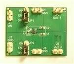
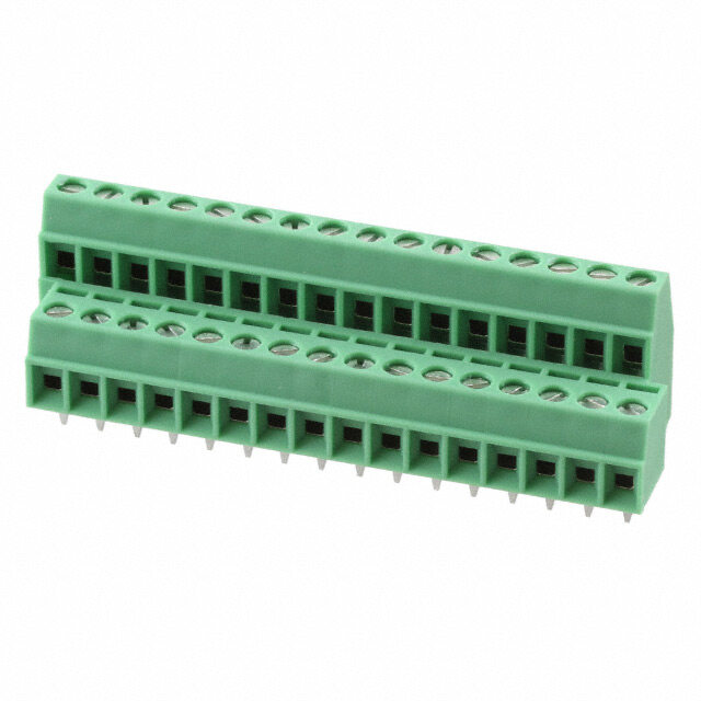
| 产品图片 |
|
| rohs | 否无铅 / 符合限制有害物质指令(RoHS)规范要求 |
| 产品系列 | 电源管理IC开发工具,Texas Instruments TLV7101828EVM-595- |
| 数据手册 | 点击此处下载产品Datasheethttp://www.ti.com/lit/pdf/slvu404 |
| 产品型号 | TLV7101828EVM-595 |
| 产品 | Evaluation Boards |
| 产品种类 | 电源管理IC开发工具 |
| 使用的IC/零件 | TLV7101828 |
| 其它名称 | 296-31050 |
| 制造商产品页 | http://www.ti.com/general/docs/suppproductinfo.tsp?distId=10&orderablePartNumber=TLV7101828EVM-595 |
| 商标 | Texas Instruments |
| 工作温度 | -40°C ~ 125°C |
| 工具用于评估 | TLV101828 |
| 工厂包装数量 | 1 |
| 所含物品 | 板 |
| 板类型 | 完全填充 |
| 标准包装 | 1 |
| 每IC通道数 | 2 - 双 |
| 电压-输入 | 2 V ~ 5.5 V |
| 电压-输出 | 1.8V,2.8V |
| 电流-输出 | 200mA,200mA |
| 稳压器类型 | 正,固定式 |
| 类型 | LDO Voltage Regulators |


- 商务部:美国ITC正式对集成电路等产品启动337调查
- 曝三星4nm工艺存在良率问题 高通将骁龙8 Gen1或转产台积电
- 太阳诱电将投资9.5亿元在常州建新厂生产MLCC 预计2023年完工
- 英特尔发布欧洲新工厂建设计划 深化IDM 2.0 战略
- 台积电先进制程称霸业界 有大客户加持明年业绩稳了
- 达到5530亿美元!SIA预计今年全球半导体销售额将创下新高
- 英特尔拟将自动驾驶子公司Mobileye上市 估值或超500亿美元
- 三星加码芯片和SET,合并消费电子和移动部门,撤换高东真等 CEO
- 三星电子宣布重大人事变动 还合并消费电子和移动部门
- 海关总署:前11个月进口集成电路产品价值2.52万亿元 增长14.8%


PDF Datasheet 数据手册内容提取
User's Guide SLVU404–September2010 TLV7101828EVM-595 This user’s guide describes the characteristics, operation, and use of the TLV7101828EVM-595 Evaluation Module (EVM) as a reference design for engineering demonstration and evaluation of the TLV710xxxx dual-channel, low-dropout (LDO) linear regulator. Included in this user’s guide are setup instructions,aschematicdiagram,layoutandthermalguidelines,abillofmaterials,andtestresults. Contents 1 Introduction .................................................................................................................. 2 2 Setup ......................................................................................................................... 2 2.1 Input/OutputConnectorsandJumperDescriptions ........................................................... 2 2.2 SolderingGuidelines............................................................................................... 2 2.3 EquipmentInterconnect ........................................................................................... 2 3 Operation..................................................................................................................... 2 4 TestResults ................................................................................................................. 3 4.1 TurnonSequence .................................................................................................. 3 4.2 OUT1LoadTransient............................................................................................. 3 4.3 OUT2LoadTransient............................................................................................. 4 5 ThermalGuidelines ......................................................................................................... 5 6 BoardLayout ................................................................................................................ 6 7 SchematicandBillofMaterials ........................................................................................... 8 7.1 Schematic ........................................................................................................... 8 7.2 BillofMaterials ..................................................................................................... 9 ListofFigures 1 TurnonSequence:Ch3VIN–Turnonto4V,Ch2OUT2–2.8-VTurnonRamp,Ch1OUT1–1.8-V TurnonRamp................................................................................................................ 3 2 Ch1OUT1-1.8-VLoadTransientResponseforVINat3.3V,Ch2OUT2–2.8-VCrosstalkResponse, Ch4OUT1LoadCurrentTransient..................................................................................... 4 3 Ch1OUT1-1.8-VCrosstalkResponse,Ch2OUT2–2.8-VTransientResponseforVINat3.3-V,Ch3 OUT2LoadCurrentTransient............................................................................................ 5 4 AssemblyLayer............................................................................................................. 6 5 LayerOneRouting.......................................................................................................... 7 6 LayerTwoRouting.......................................................................................................... 7 7 BottomLayerRouting...................................................................................................... 8 8 TLV7101828EVM-595Schematic........................................................................................ 8 ListofTables 1 ThermalResistance,q_ja,andMaximumPowerDissipation........................................................ 6 2 TLV7101828EVM-595BillofMaterials................................................................................... 9 SLVU404–September2010 TLV7101828EVM-595 1 SubmitDocumentationFeedback Copyright©2010,TexasInstrumentsIncorporated
Introduction www.ti.com 1 Introduction TheTexasInstrumentsTLV7101828EVM-595EVMhelpsdesignersevaluatetheoperationand performanceoftheTLV710xxxxfamilyoflinearregulatorsforpossibleuseintheircircuitapplications. Thisparticularintegratedcircuit(IC)configurationcontainstwoseparatelinearregulatorswithseparate thermalandcurrent-limitshutdowns,andseparateenablecircuitryinanextremelysmall,1.5-mmx 1.5-mmpackage.Eachchannelissimultaneouslycapableofdeliveringupto200mAofloadcurrent dependingonthermal/layoutconsiderationsandinput/outputvoltagedropsacrossthepart.The TLV710xxxxdoesnotrequireaninputcapacitor,andtheoutputcapacitoronlyneedbe0.1µF(effective minimum)forstability;however,forconservativedesignpracticeaccountingforwidelyvaryingnoise environmentsanddynamicline/loadconditions,a1-µFcapacitorhasbeenemployedattheinputandboth outputports. 2 Setup ThissectiondescribesthejumpersandconnectorsontheEVMaswellashowtoproperlyconnect,set up,andusetheTLV7101828EVM-595. 2.1 Input/Output Connectors and Jumper Descriptions • J1(VIN)– Thepositiveinputsupplyvoltageconnector.Twistthepositiveinputleadandgroundlead, andkeepthemasshortaspossibletominimizeEMItransmission.Additionalbulkcapacitancemustbe addedbetweenJ1andJ2ifthesupplyleadsaregreaterthansixinches.Anadditional47-µFor greatercapacitorimprovesthetransientresponseoftheTLV710xxxxandreducesringingontheinput duetolongwireconnections. • J2(GND)–Ground-returnconnectionfortheinputpowersupply. • J3(OUT1)– Channel1,positivevoltage,outputconnector. • J4(GND)–Channel1,outputground-returnconnector. • J5(OUT2)– Channel2,positivevoltage,outputconnector. • J6(GND)–Channel2,outputground-returnconnector. • JP1(EN1)–Channel1,outputenable.Toenablethechannel1output,connectajumpertoshortthe VINpin1totheEN1centerpin2.Todisablethechannel1output,connectthejumperbetweenthe EN1centerpin2andGNDpin3. • JP2(EN2)–Channel2,outputenable.Toenablethechannel2output,connectajumpertoshortthe VINpin1totheEN2centerpin2.Todisablethechannel1output,connectthejumperbetweenthe EN2centerpin2andGNDpin3. 2.2 Soldering Guidelines Anysolderre-worktomodifytheEVMforthepurposeofrepairorotherapplicationreasonsmustbe performedusingahot-airsystemtoavoiddamagingtheintegratedcircuitICespecially. 2.3 Equipment Interconnect • Turnofftheinputpowersupplyafterverifyingthatitsoutputvoltageislessthan5.5V.Connectthe positivevoltageleadfrominputpowersupplytotheJP1connectoroftheEVM.Connecttheground leadfromtheinputpowersupplytoJP2oftheEVM. • Connecta0-mAto200-mAloadbetweenthepositiveoutputofchannel1,OUT1–JP3,andthe channel1groundconnection,JP4. • Connecta0-mAto200-mAloadbetweenthepositiveoutputofchannel2,OUT2–JP5,andthe channel2groundconnection,JP6. • DisableOUT1byjumperingJP1–EN1toGND. • DisableOUT2byjumperingJP2–EN2toGND. 3 Operation • Turnontheinputpowersupply.Forinitialoperation,itisrecommendedthattheinputpowersupply, VIN– JP1,besetto3.6V. • EnableOUT1andorOUT2asdesired– reconnectthejumperonJP1(andorJP2)fromEN1(EN2) 2 TLV7101828EVM-595 SLVU404–September2010 SubmitDocumentationFeedback Copyright©2010,TexasInstrumentsIncorporated
www.ti.com TestResults toVIN. • VarytherespectiveloadsandVINvoltagesasnecessaryfortestpurposes. 4 Test Results ThissectionprovidestypicalperformancewaveformsfortheTLV7101828EVM-595printed-circuitboard. 4.1 Turnon Sequence Figure1showstheturnonsequenceforthecasewheretheenableisconnectedtotheVINvoltage.The VINturnonvoltagerisesto4Vfollowedbyanapproximate50-µsdelayprecedingthesimultaneousramp upofthetwooutputvoltages.Thesetwooutputvoltagesarecompletelyindependent,andtheramprates aresetbydesign.Theoutputvoltagestartuprampisnotloaddependant. Figure1.TurnonSequence:Ch3VIN– Turnonto4V,Ch2OUT2– 2.8-VTurnonRamp,Ch1OUT1 – 1.8-VTurnonRamp 4.2 OUT 1 Load Transient Figure2showstheloadtransientresponse–oscilloscopechannel1 –fora90-mAto180-mAload transientappliedtoOUT1(1.8-Voutput).Oscilloscopechannel2showsthecrosstalkcouplingfromthe LDOOUT1channelintoOUT2,whereOUT2isloadedwith200mAdc.Oscilloscopechannel4shows theapproximateloadcurrenttransient. SLVU404–September2010 TLV7101828EVM-595 3 SubmitDocumentationFeedback Copyright©2010,TexasInstrumentsIncorporated
TestResults www.ti.com Figure2.Ch1OUT1-1.8-VLoadTransientResponseforVINat3.3V,Ch2OUT2– 2.8-VCrosstalk Response,Ch4OUT1LoadCurrentTransient 4.3 OUT 2 Load Transient Figure2showstheloadtransientresponse–oscilloscopechannel1 –fora90-mAto180-mAload transientappliedtoOUT1(1.8-Voutput).Oscilloscopechannel2showsthecrosstalkcouplingfromthe LDOOUT1channelintoOUT2,whereOUT2isloadedwith200mAdc.Oscilloscopechannel4 illustratestheapproximateloadcurrenttransient. Figure3showstheloadtransientresponse–oscilloscopechannel2 –fora90-mAto180-mAload transientappliedtoOUT2(2.8-Voutput).Oscilloscopechannel1showsthecrosstalkcouplingfromthe LDOOUT2channelintoOUT1,whereOUT1isloadedwith200mAdc.Oscilloscopechannel4 illustratestheapproximateloadcurrenttransient. 4 TLV7101828EVM-595 SLVU404–September2010 SubmitDocumentationFeedback Copyright©2010,TexasInstrumentsIncorporated
www.ti.com ThermalGuidelines Figure3.Ch1OUT1-1.8-VCrosstalkResponse,Ch2OUT2– 2.8-VTransientResponseforVINat3.3-V, Ch3OUT2LoadCurrentTransient 5 Thermal Guidelines Thermalmanagementisakeycomponentofdesignofanypowerconverterandisespeciallyimportant whenthepowerdissipationintheLDOishigh.Usethefollowingformulatoapproximatethemaximum powerdissipationfortheparticularambienttemperature: T_j=T_a+Pdxq_ja whereT_jisthejunctiontemperature,T_aistheambienttemperature,P_disthepowerdissipationinthe device,andq_jaisthethermalresistancefromjunctiontoambient.Alltemperaturesareindegrees Celsius.Themaximumsiliconjunctiontemperature,T_j,mustnotbeallowedtoexceed150°C.Thelayout designofthecoppertraceandplaneareasmustbeusedeffectivelyasthermalsinksinordertoavoidT_j fromexceedingtheabsolutemaximumratingunderalltemperatureconditionsandvoltageconditions acrossthepart. NotethatbecausetheTLV710xxxxconsistsoftwoseparateLDOsinthesamepackage,thetotal dissipatedpower,P_d,isthesumofthepowerdissipatedineachLDOchannelseparatelycalculatedas follows: P_d=(Vin–Vout_1)xIout_1+(Vin –Vout_2)xIout_2 whereVinistheinputsupplyvoltageattheVINconnector,Vout_1istheoutputvoltageatOUT1,Iout_1 istheoutputloadcurrentfromOUT1,Vout_2istheoutputvoltageatOUT_2,andIout_2istheoutput loadcurrentfromOUT2. ThethermaldesignofthePCBmustbecarefullyconsideredinthelayout.Itisdifficulttocalculatethe thermalresistanceforacustomlayoutwithauniquecopperareaattachedtoeachpinoftheIC.repeats informationfromtheDissipationRatingsTableoftheTPS710xxdatasheetforcomparisonwiththe thermalresistance,q_ja,calculatedforthisEVMtoshowthewidevariationinthermalresistancesfor givencopperareas.Thehigh-KvalueisdeterminedusingastandardJEDEChigh-k(2s2p)boardwith dimensionsof3inchx30inchwith1-ounceinternalpowerandgroundplanesand2-ouncecoppertraces ontopandbottomoftheboard. SLVU404–September2010 TLV7101828EVM-595 5 SubmitDocumentationFeedback Copyright©2010,TexasInstrumentsIncorporated
BoardLayout www.ti.com Table1.ThermalResistance,q_ja,andMaximumPowerDissipation MaximumDissipation MaximumDissipation Board Package q_ja WithoutDerating WithoutDerating (T =25°C) (T =70d°C) A A High-K DSE 206°C/W 485mW 269mW TPS710xxEVM-595 DSE 120°C/W 833mW 458mW ThethermalresistancefortheTPS710xxEVM-595,q_ja,isthemeasuredvalueforthisparticularlayout scheme.Themaximumpowerdissipationisproportionaltothevolumeofcoppervolumeconnectedtothe package. 6 Board Layout Figure4.AssemblyLayer 6 TLV7101828EVM-595 SLVU404–September2010 SubmitDocumentationFeedback Copyright©2010,TexasInstrumentsIncorporated
www.ti.com BoardLayout Figure5.LayerOneRouting Figure6.LayerTwoRouting SLVU404–September2010 TLV7101828EVM-595 7 SubmitDocumentationFeedback Copyright©2010,TexasInstrumentsIncorporated
SchematicandBillofMaterials www.ti.com S T N E M U SR A T XS EN T I Figure7.BottomLayerRouting 7 Schematic and Bill of Materials 7.1 Schematic Figure8.TLV7101828EVM-595Schematic 8 TLV7101828EVM-595 SLVU404–September2010 SubmitDocumentationFeedback Copyright©2010,TexasInstrumentsIncorporated
www.ti.com SchematicandBillofMaterials 7.2 Bill of Materials Table2.TLV7101828EVM-595BillofMaterials Count RefDes Value Description Size PartNumber MFR 3 C1-C3 1µF Capacitor,Ceramic,6.3V,X5R,20% 603 STD STD 6 J1-J6 PEC02SAAN Header,2-pin,100milspacing 0.100inchx2 PEC02SAAN Sullins 2 JP1,JP2 PEC03SAAN Header,3-pin,100milspacing 0.100inchx3 PEC03SAAN Sullins 1 U1 TLV7101828DSE IC,Dual200mA,LDORegulator SON-6 TLV7101828DSE TI 1 N/A PCB,FR-4,2-Layer,SMOBC,1.052in.x HPA595 TI 1.290in.x0.062in. 2 N/A Shunt,Open-top 151-8000 Kobiconn Notes:1. TheseassembliesareESDsensitive,ESDprecautionsshallbeobserved. 2. 2.Theseassembliesmustbecleanandfreefromfluxandallcontaminants. Useofnocleanfluxisnotacceptable. 3. TheseassembliesmustcomplywithworkmanshipstandardsIPC-A-610Class2. 4. Refdesignatorsmarkedwithanasterisk('**')cannotbesubstituted. AllothercomponentscanbesubstitutedwithequivalentMFG'scomponents. 5. DonotseparatePCB SLVU404–September2010 TLV7101828EVM-595 9 SubmitDocumentationFeedback Copyright©2010,TexasInstrumentsIncorporated
EvaluationBoard/KitImportantNotice TexasInstruments(TI)providestheenclosedproduct(s)underthefollowingconditions: Thisevaluationboard/kitisintendedforuseforENGINEERINGDEVELOPMENT,DEMONSTRATION,OREVALUATION PURPOSESONLYandisnotconsideredbyTItobeafinishedend-productfitforgeneralconsumeruse.Personshandlingthe product(s)musthaveelectronicstrainingandobservegoodengineeringpracticestandards.Assuch,thegoodsbeingprovidedare notintendedtobecompleteintermsofrequireddesign-,marketing-,and/ormanufacturing-relatedprotectiveconsiderations, includingproductsafetyandenvironmentalmeasurestypicallyfoundinendproductsthatincorporatesuchsemiconductor componentsorcircuitboards.Thisevaluationboard/kitdoesnotfallwithinthescopeoftheEuropeanUniondirectivesregarding electromagneticcompatibility,restrictedsubstances(RoHS),recycling(WEEE),FCC,CEorUL,andthereforemaynotmeetthe technicalrequirementsofthesedirectivesorotherrelateddirectives. Shouldthisevaluationboard/kitnotmeetthespecificationsindicatedintheUser’sGuide,theboard/kitmaybereturnedwithin30 daysfromthedateofdeliveryforafullrefund.THEFOREGOINGWARRANTYISTHEEXCLUSIVEWARRANTYMADEBY SELLERTOBUYERANDISINLIEUOFALLOTHERWARRANTIES,EXPRESSED,IMPLIED,ORSTATUTORY,INCLUDING ANYWARRANTYOFMERCHANTABILITYORFITNESSFORANYPARTICULARPURPOSE. Theuserassumesallresponsibilityandliabilityforproperandsafehandlingofthegoods.Further,theuserindemnifiesTIfromall claimsarisingfromthehandlingoruseofthegoods.Duetotheopenconstructionoftheproduct,itistheuser’sresponsibilityto takeanyandallappropriateprecautionswithregardtoelectrostaticdischarge. EXCEPTTOTHEEXTENTOFTHEINDEMNITYSETFORTHABOVE,NEITHERPARTYSHALLBELIABLETOTHEOTHER FORANYINDIRECT,SPECIAL,INCIDENTAL,ORCONSEQUENTIALDAMAGES. TIcurrentlydealswithavarietyofcustomersforproducts,andthereforeourarrangementwiththeuserisnotexclusive. TIassumesnoliabilityforapplicationsassistance,customerproductdesign,softwareperformance,orinfringementof patentsorservicesdescribedherein. PleasereadtheUser’sGuideand,specifically,theWarningsandRestrictionsnoticeintheUser’sGuidepriortohandlingthe product.Thisnoticecontainsimportantsafetyinformationabouttemperaturesandvoltages.ForadditionalinformationonTI’s environmentaland/orsafetyprograms,pleasecontacttheTIapplicationengineerorvisitwww.ti.com/esh. NolicenseisgrantedunderanypatentrightorotherintellectualpropertyrightofTIcoveringorrelatingtoanymachine,process,or combinationinwhichsuchTIproductsorservicesmightbeorareused. FCCWarning Thisevaluationboard/kitisintendedforuseforENGINEERINGDEVELOPMENT,DEMONSTRATION,OREVALUATION PURPOSESONLYandisnotconsideredbyTItobeafinishedend-productfitforgeneralconsumeruse.Itgenerates,uses,and canradiateradiofrequencyenergyandhasnotbeentestedforcompliancewiththelimitsofcomputingdevicespursuanttopart15 ofFCCrules,whicharedesignedtoprovidereasonableprotectionagainstradiofrequencyinterference.Operationofthis equipmentinotherenvironmentsmaycauseinterferencewithradiocommunications,inwhichcasetheuserathisownexpense willberequiredtotakewhatevermeasuresmayberequiredtocorrectthisinterference. EVMWarningsandRestrictions ItisimportanttooperatethisEVMwithintheinputvoltagerangeof2Vto5.5Vandtheoutputvoltagerangeof1.2Vto4.8V. Exceedingthespecifiedinputrangemaycauseunexpectedoperationand/orirreversibledamagetotheEVM.Ifthereare questionsconcerningtheinputrange,pleasecontactaTIfieldrepresentativepriortoconnectingtheinputpower. Applyingloadsoutsideofthespecifiedoutputrangemayresultinunintendedoperationand/orpossiblepermanentdamagetothe EVM.PleaseconsulttheEVMUser'sGuidepriortoconnectinganyloadtotheEVMoutput.Ifthereisuncertaintyastotheload specification,pleasecontactaTIfieldrepresentative. Duringnormaloperation,somecircuitcomponentsmayhavecasetemperaturesgreaterthan130°C.TheEVMisdesignedto operateproperlywithcertaincomponentsabove130°Caslongastheinputandoutputrangesaremaintained.Thesecomponents includebutarenotlimitedtolinearregulators,switchingtransistors,passtransistors,andcurrentsenseresistors.Thesetypesof devicescanbeidentifiedusingtheEVMschematiclocatedintheEVMUser'sGuide.Whenplacingmeasurementprobesnear thesedevicesduringoperation,pleasebeawarethatthesedevicesmaybeverywarmtothetouch. MailingAddress:TexasInstruments,PostOfficeBox655303,Dallas,Texas75265 Copyright©2010,TexasInstrumentsIncorporated
IMPORTANTNOTICE TexasInstrumentsIncorporatedanditssubsidiaries(TI)reservetherighttomakecorrections,modifications,enhancements,improvements, andotherchangestoitsproductsandservicesatanytimeandtodiscontinueanyproductorservicewithoutnotice.Customersshould obtainthelatestrelevantinformationbeforeplacingordersandshouldverifythatsuchinformationiscurrentandcomplete.Allproductsare soldsubjecttoTI’stermsandconditionsofsalesuppliedatthetimeoforderacknowledgment. TIwarrantsperformanceofitshardwareproductstothespecificationsapplicableatthetimeofsaleinaccordancewithTI’sstandard warranty.TestingandotherqualitycontroltechniquesareusedtotheextentTIdeemsnecessarytosupportthiswarranty.Exceptwhere mandatedbygovernmentrequirements,testingofallparametersofeachproductisnotnecessarilyperformed. TIassumesnoliabilityforapplicationsassistanceorcustomerproductdesign.Customersareresponsiblefortheirproductsand applicationsusingTIcomponents.Tominimizetherisksassociatedwithcustomerproductsandapplications,customersshouldprovide adequatedesignandoperatingsafeguards. TIdoesnotwarrantorrepresentthatanylicense,eitherexpressorimplied,isgrantedunderanyTIpatentright,copyright,maskworkright, orotherTIintellectualpropertyrightrelatingtoanycombination,machine,orprocessinwhichTIproductsorservicesareused.Information publishedbyTIregardingthird-partyproductsorservicesdoesnotconstitutealicensefromTItousesuchproductsorservicesora warrantyorendorsementthereof.Useofsuchinformationmayrequirealicensefromathirdpartyunderthepatentsorotherintellectual propertyofthethirdparty,oralicensefromTIunderthepatentsorotherintellectualpropertyofTI. ReproductionofTIinformationinTIdatabooksordatasheetsispermissibleonlyifreproductioniswithoutalterationandisaccompanied byallassociatedwarranties,conditions,limitations,andnotices.Reproductionofthisinformationwithalterationisanunfairanddeceptive businesspractice.TIisnotresponsibleorliableforsuchaltereddocumentation.Informationofthirdpartiesmaybesubjecttoadditional restrictions. ResaleofTIproductsorserviceswithstatementsdifferentfromorbeyondtheparametersstatedbyTIforthatproductorservicevoidsall expressandanyimpliedwarrantiesfortheassociatedTIproductorserviceandisanunfairanddeceptivebusinesspractice.TIisnot responsibleorliableforanysuchstatements. TIproductsarenotauthorizedforuseinsafety-criticalapplications(suchaslifesupport)whereafailureoftheTIproductwouldreasonably beexpectedtocauseseverepersonalinjuryordeath,unlessofficersofthepartieshaveexecutedanagreementspecificallygoverning suchuse.Buyersrepresentthattheyhaveallnecessaryexpertiseinthesafetyandregulatoryramificationsoftheirapplications,and acknowledgeandagreethattheyaresolelyresponsibleforalllegal,regulatoryandsafety-relatedrequirementsconcerningtheirproducts andanyuseofTIproductsinsuchsafety-criticalapplications,notwithstandinganyapplications-relatedinformationorsupportthatmaybe providedbyTI.Further,BuyersmustfullyindemnifyTIanditsrepresentativesagainstanydamagesarisingoutoftheuseofTIproductsin suchsafety-criticalapplications. TIproductsareneitherdesignednorintendedforuseinmilitary/aerospaceapplicationsorenvironmentsunlesstheTIproductsare specificallydesignatedbyTIasmilitary-gradeor"enhancedplastic."OnlyproductsdesignatedbyTIasmilitary-grademeetmilitary specifications.BuyersacknowledgeandagreethatanysuchuseofTIproductswhichTIhasnotdesignatedasmilitary-gradeissolelyat theBuyer'srisk,andthattheyaresolelyresponsibleforcompliancewithalllegalandregulatoryrequirementsinconnectionwithsuchuse. TIproductsareneitherdesignednorintendedforuseinautomotiveapplicationsorenvironmentsunlessthespecificTIproductsare designatedbyTIascompliantwithISO/TS16949requirements.Buyersacknowledgeandagreethat,iftheyuseanynon-designated productsinautomotiveapplications,TIwillnotberesponsibleforanyfailuretomeetsuchrequirements. FollowingareURLswhereyoucanobtaininformationonotherTexasInstrumentsproductsandapplicationsolutions: Products Applications Amplifiers amplifier.ti.com Audio www.ti.com/audio DataConverters dataconverter.ti.com Automotive www.ti.com/automotive DLP®Products www.dlp.com Communicationsand www.ti.com/communications Telecom DSP dsp.ti.com Computersand www.ti.com/computers Peripherals ClocksandTimers www.ti.com/clocks ConsumerElectronics www.ti.com/consumer-apps Interface interface.ti.com Energy www.ti.com/energy Logic logic.ti.com Industrial www.ti.com/industrial PowerMgmt power.ti.com Medical www.ti.com/medical Microcontrollers microcontroller.ti.com Security www.ti.com/security RFID www.ti-rfid.com Space,Avionics& www.ti.com/space-avionics-defense Defense RF/IFandZigBee®Solutions www.ti.com/lprf VideoandImaging www.ti.com/video Wireless www.ti.com/wireless-apps MailingAddress:TexasInstruments,PostOfficeBox655303,Dallas,Texas75265 Copyright©2010,TexasInstrumentsIncorporated