ICGOO在线商城 > 集成电路(IC) > PMIC - 电压基准 > TLV431BCDBVT
 Datasheet下载
- 型号: TLV431BCDBVT
- 制造商: Texas Instruments
- 库位|库存: xxxx|xxxx
- 要求:
| 数量阶梯 | 香港交货 | 国内含税 |
| +xxxx | $xxxx | ¥xxxx |
查看当月历史价格
查看今年历史价格
TLV431BCDBVT产品简介:
ICGOO电子元器件商城为您提供TLV431BCDBVT由Texas Instruments设计生产,在icgoo商城现货销售,并且可以通过原厂、代理商等渠道进行代购。 TLV431BCDBVT价格参考¥3.37-¥8.32。Texas InstrumentsTLV431BCDBVT封装/规格:PMIC - 电压基准, 分流器 电压基准 IC 6V ±0.5% 15mA SOT-23-5。您可以下载TLV431BCDBVT参考资料、Datasheet数据手册功能说明书,资料中有TLV431BCDBVT 详细功能的应用电路图电压和使用方法及教程。
TLV431BCDBVT 是 Texas Instruments(德州仪器)生产的一款可调式精密稳压器,属于 PMIC(电源管理集成电路)中的电压基准类别。它广泛应用于需要高精度电压基准和简单稳压功能的场景。以下是其主要应用场景:

 1. 电源管理
   - TLV431 可用作简单的线性稳压器,为低功耗设备提供稳定的输出电压。
   - 在电池供电系统中,作为电压基准源,确保电路在不同电池电量下仍能正常工作。

 2. 电压基准
   - 作为 ADC(模数转换器)或 DAC(数模转换器)的参考电压源,提供高精度的基准电压。
   - 在传感器信号调理电路中,为放大器或比较器提供精确的基准电压。

 3. 过压/欠压保护
   - 利用 TLV431 的可调特性,设计过压或欠压检测电路,保护后端负载免受异常电压影响。
   - 例如,在 USB 电源管理中,用于检测输入电压是否超出安全范围。

 4. 电流调节
   - 结合电阻分压网络,实现恒流源设计,常用于 LED 驱动或电流校准电路。
   - 在充电电路中,用作电流限制元件,确保充电过程的安全性和稳定性。

 5. 温度补偿电路
   - TLV431 的高精度和低温漂特性使其适用于需要温度补偿的场景,例如精密测量设备或环境监测系统。

 6. 通信与工业控制
   - 在通信模块中,作为电源监控或信号调理的核心元件。
   - 工业自动化领域中,用于 PLC(可编程逻辑控制器)或其他嵌入式系统的电压基准。

 特性优势
- 低静态电流:适合电池供电设备,延长续航时间。
- 宽工作电压范围:支持 1.25V 至 36V 输入电压,适应多种应用场景。
- 高精度:典型参考电压为 1.24V,误差小于 1%,满足精密需求。
- 小型封装:SOT-23 封装节省空间,适合紧凑型设计。

综上,TLV431BCDBVT 广泛应用于消费电子、工业控制、通信设备、医疗仪器等领域,特别是在需要高精度电压基准和简单稳压功能的场合表现出色。
| 参数 | 数值 |
| 产品目录 | 集成电路 (IC)半导体 |
| 描述 | IC VREF SHUNT PREC ADJ SOT23-5参考电压 Lo-Vtg Adj Precision Shunt Regulator |
| 产品分类 | |
| 品牌 | Texas Instruments |
| 产品手册 | |
| 产品图片 |
|
| rohs | 符合RoHS无铅 / 符合限制有害物质指令(RoHS)规范要求 |
| 产品系列 | 电源管理 IC,参考电压,Texas Instruments TLV431BCDBVT- |
| 数据手册 | |
| 产品型号 | TLV431BCDBVT |
| PCN设计/规格 | |
| 串联VREF—输入电压—最大值 | 7 V |
| 产品种类 | 参考电压 |
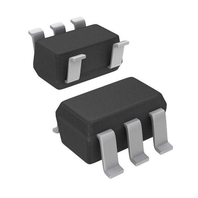
| 供应商器件封装 | SOT-23-5 |
| 其它名称 | 296-32397-6 |
| 分流电流—最大值 | 15 mA |
| 分流电流—最小值 | 80 uA |
| 初始准确度 | 0.5 % |
| 包装 | Digi-Reel® |
| 单位重量 | 15.800 mg |
| 参考类型 | Shunt Adjustable Precision References |
| 商标 | Texas Instruments |
| 安装类型 | 表面贴装 |
| 安装风格 | SMD/SMT |
| 容差 | ±0.5% |
| 封装 | Reel |
| 封装/外壳 | SC-74A,SOT-753 |
| 封装/箱体 | SOT-23-5 |
| 工作温度 | 0°C ~ 70°C |
| 工厂包装数量 | 250 |
| 最大工作温度 | + 70 C |
| 最小工作温度 | 0 C |
| 标准包装 | 1 |
| 温度系数 | 138ppm/°C |
| 电压-输入 | - |
| 电压-输出 | 1.24 V ~ 6 V |
| 电流-输出 | 15mA |
| 电流-阴极 | 100µA |
| 电流-静态 | - |
| 系列 | TLV431B |
| 输出电压 | Adjustable |
| 通道数 | 1 |


- 商务部:美国ITC正式对集成电路等产品启动337调查
- 曝三星4nm工艺存在良率问题 高通将骁龙8 Gen1或转产台积电
- 太阳诱电将投资9.5亿元在常州建新厂生产MLCC 预计2023年完工
- 英特尔发布欧洲新工厂建设计划 深化IDM 2.0 战略
- 台积电先进制程称霸业界 有大客户加持明年业绩稳了
- 达到5530亿美元!SIA预计今年全球半导体销售额将创下新高
- 英特尔拟将自动驾驶子公司Mobileye上市 估值或超500亿美元
- 三星加码芯片和SET,合并消费电子和移动部门,撤换高东真等 CEO
- 三星电子宣布重大人事变动 还合并消费电子和移动部门
- 海关总署:前11个月进口集成电路产品价值2.52万亿元 增长14.8%


PDF Datasheet 数据手册内容提取
Product Order Technical Tools & Support & Folder Now Documents Software Community TLV431,TLV431A,TLV431B SLVS139X–JULY1996–REVISEDMAY2018 TLV431x Low-Voltage Adjustable Precision Shunt Regulator 1 Features 3 Description • Low-VoltageOperation,V =1.24V The TLV431 device is a low-voltage 3-terminal 1 REF adjustable voltage reference with specified thermal • AdjustableOutputVoltage,V =V to6V O REF stability over applicable industrial and commercial • ReferenceVoltageTolerancesat25°C temperature ranges. Output voltage can be set to any – 0.5%forTLV431B value between VREF (1.24 V) and 6 V with two external resistors (see the Parameter Measurement – 1%forTLV431A Information section). These devices operate from a – 1.5%forTLV431 lower voltage (1.24 V) than the widely used TL431 • TypicalTemperatureDrift andTL1431shunt-regulatorreferences. – 4mV(0°Cto70°C) When used with an optocoupler, the TLV431 device – 6mV(–40°Cto85°C) is an ideal voltage reference in isolated feedback circuits for 3-V to 3.3-V switching-mode power – 11mV(–40°Cto125°C) supplies. These devices have a typical output • LowOperationalCathodeCurrent,80µATypical impedance of 0.25 Ω. Active output circuitry provides • 0.25-Ω TypicalOutputImpedance a very sharp turnon characteristic, making them excellent replacements for low-voltage Zener diodes • Ultra-SmallSC-70PackageOffers40%Smaller in many applications, including on-board regulation FootprintThanSOT-23-3 andadjustablepowersupplies. • SeeTLVH431andTLVH432for: – WiderV (1.24Vto18V)andI (80mA) DeviceInformation(1) KA K – AdditionalSOT-89Package PARTNUMBER PACKAGE(PIN) BODYSIZE(NOM) – MultiplePinoutsforSOT-23-3andSOT-89 SOT-23(3) 2.90mm×1.30mm Packages SOT-23(5) 2.90mm×1.60mm • OnProductsComplianttoMIL-PRF-38535, TLV431x SC70(6) 2.00mm×1.25mm AllParametersAreTestedUnlessOtherwise TO-92(3) 4.30mm×4.30mm Noted.OnAllOtherProducts,Production SOIC(8) 4.90mm×3.90mm ProcessingDoesNotNecessarilyIncludeTesting (1) For all available packages, see the orderable addendum at ofAllParameters. theendofthedatasheet. 2 Applications SimplifiedSchematic • AdjustableVoltageandCurrentReferencing Input VO • SecondarySideRegulationinFlybackSMPSs IK • ZenerReplacement • VoltageMonitoring • ComparatorWithIntegratedReference VREF 1 An IMPORTANT NOTICE at the end of this data sheet addresses availability, warranty, changes, use in safety-critical applications, intellectualpropertymattersandotherimportantdisclaimers.PRODUCTIONDATA.
TLV431,TLV431A,TLV431B SLVS139X–JULY1996–REVISEDMAY2018 www.ti.com Table of Contents 1 Features.................................................................. 1 8.3 FeatureDescription.................................................17 2 Applications........................................................... 1 8.4 DeviceFunctionalModes........................................18 3 Description............................................................. 1 9 ApplicationsandImplementation...................... 19 4 RevisionHistory..................................................... 2 9.1 ApplicationInformation............................................19 9.2 TypicalApplications................................................20 5 PinConfigurationandFunctions......................... 3 10 PowerSupplyRecommendations..................... 24 6 Specifications......................................................... 4 11 Layout................................................................... 24 6.1 AbsoluteMaximumRatings......................................4 6.2 ESDRatings..............................................................4 11.1 LayoutGuidelines.................................................24 6.3 RecommendedOperatingConditions.......................4 11.2 LayoutExample....................................................24 6.4 ThermalInformation..................................................4 12 DeviceandDocumentationSupport................. 25 6.5 ElectricalCharacteristicsforTLV431........................5 12.1 DocumentationSupport........................................25 6.6 ElectricalCharacteristicsforTLV431A.....................6 12.2 RelatedLinks........................................................25 6.7 ElectricalCharacteristicsforTLV431B.....................7 12.3 ReceivingNotificationofDocumentationUpdates25 6.8 TypicalCharacteristics..............................................8 12.4 CommunityResources..........................................25 7 ParameterMeasurementInformation................16 12.5 Trademarks...........................................................25 12.6 ElectrostaticDischargeCaution............................25 8 DetailedDescription............................................ 17 12.7 Glossary................................................................25 8.1 Overview.................................................................17 13 Mechanical,Packaging,andOrderable 8.2 FunctionalBlockDiagram.......................................17 Information........................................................... 25 4 Revision History ChangesfromRevisionW(March2018)toRevisionX Page • Changedfigure18 ............................................................................................................................................................... 14 ChangesfromRevisionV(January2015)toRevisionW Page • ChangedcrossreferencelinkintheDescriptionsection ....................................................................................................... 1 • ChangedtheStabilityBoundaryConditionsgraph.............................................................................................................. 13 • AddedthePhaseMarginvsCapacitiveLoadV =V (1.25V),T =25°Cgraph........................................................... 14 KA REF A • AddedthePhaseMarginvsCapacitiveLoadV =2.50V,T =25°Cgraph...................................................................... 14 KA A • AddedthePhaseMarginvsCapacitiveLoadV =5.00V,T =25°Cgraph...................................................................... 15 KA A • AddedDocumentationSupportsection ............................................................................................................................... 25 • AddedReceivingNotificationofDocumentationUpdatessection ...................................................................................... 25 • AddedCommunityResourcessection ................................................................................................................................ 25 ChangesfromRevisionU(January2014)toRevisionV Page • AddedApplications,DeviceInformationtable,PinFunctionstable,ESDRatingstable,ThermalInformationtable, FeatureDescriptionsection,DeviceFunctionalModes,ApplicationandImplementationsection,PowerSupply Recommendationssection,Layoutsection,DeviceandDocumentationSupportsection,andMechanical, Packaging,andOrderableInformationsection...................................................................................................................... 1 ChangesfromRevisionT(June2007)toRevisionU Page • UpdateddocumenttonewTIdatasheetformat.................................................................................................................... 1 • DeletedOrderingInformationtable........................................................................................................................................ 1 • UpdatedFeatures................................................................................................................................................................... 1 2 SubmitDocumentationFeedback Copyright©1996–2018,TexasInstrumentsIncorporated ProductFolderLinks:TLV431 TLV431A TLV431B
TLV431,TLV431A,TLV431B www.ti.com SLVS139X–JULY1996–REVISEDMAY2018 5 Pin Configuration and Functions D(SOIC)PACKAGE DBV(SOT-23-5)PACKAGE DBZ(SOT-23-3)PACKAGE (TOPVIEW) (TOPVIEW) (TOPVIEW) CATHODE 1 8 REF NC 1 5 ANODE REF 1 ANODE 2 7 ANODE ∗ 2 3 ANODE ANODE 3 6 ANODE CATHODE 3 4 REF CATHODE 2 NC 4 5 NC NC−No internal connection ∗ ForTLV431,TLV431A:NC−Nointernalconnection ∗ ForTLV431B: Pin2isattachedtoSubstrateand must be connected toANODE or left open. PK(SOT-89)PACKAGE DCK(SC-70)PACKAGE LP(TO-92/TO-226)PACKAGE (TOPVIEW) (TOPVIEW) (TOPVIEW) 3 CATHODE CATHODE 1 6 ANODE CATHODE ANODE 2 ANODE NC 2 5 NC ANODE REF 3 4 NC 1 REF REF NC−No internal connection PinFunctions PIN TYPE DESCRIPTION NAME DBZ DBV PK D LP DCK CATHODE 2 3 3 1 1 1 I/O ShuntCurrent/Voltageinput REF 1 4 1 8 3 3 I Thresholdrelativetocommonanode ANODE 3 5 2 2,3,6,7 2 6 O Commonpin,normallyconnectedtoground NC — 1 — 4,5 — 2,4,5 I NoInternalConnection * — 2 — — — — I SubstrateConnection Copyright©1996–2018,TexasInstrumentsIncorporated SubmitDocumentationFeedback 3 ProductFolderLinks:TLV431 TLV431A TLV431B
TLV431,TLV431A,TLV431B SLVS139X–JULY1996–REVISEDMAY2018 www.ti.com 6 Specifications 6.1 Absolute Maximum Ratings overoperatingfree-airtemperaturerange(unlessotherwisenoted)(1) MIN MAX UNIT V Cathodevoltage(2) 7 V KA I Continuouscathodecurrent –20 20 mA K I Referencecurrent –0.05 3 mA ref Operatingvirtualjunctiontemperature 150 °C T Storagetemperature –65 150 °C stg (1) StressesbeyondthoselistedunderAbsoluteMaximumRatingsmaycausepermanentdamagetothedevice.Thesearestressratings only,andfunctionaloperationofthedeviceattheseoranyotherconditionsbeyondthoseindicatedunderRecommendedOperating Conditionsisnotimplied.Exposuretoabsolute-maximum-ratedconditionsforextendedperiodsmayaffectdevicereliability. (2) Voltagevaluesarewithrespecttotheanodeterminal,unlessotherwisenoted. 6.2 ESD Ratings PARAMETER DEFINITION VALUE UNIT Electrostatic Humanbodymodel(HBM),perANSI/ESDA/JEDECJS-001,allpins(1) ±2000 V V (ESD) discharge Chargeddevicemodel(CDM),perJEDECspecificationJESD22-C101,allpins(2) ±1000 (1) JEDECdocumentJEP155statesthat500-VHBMallowssafemanufacturingwithastandardESDcontrolprocess. (2) JEDECdocumentJEP157statesthat250-VCDMallowssafemanufacturingwithastandardESDcontrolprocess. 6.3 Recommended Operating Conditions overoperatingfree-airtemperaturerange(unlessotherwisenoted) MIN MAX UNIT V Cathodevoltage V 6 V KA REF I Cathodecurrent 0.1 15 mA K TLV431_C 0 70 T Operatingfree-airtemperature TLV431_I –40 85 °C A TLV431_Q –40 125 6.4 Thermal Information TLV431x THERMALMETRIC(1) DCK D PK DBV DBZ LP UNIT 6PINS 8PINS 3PINS 5PINS 3PINS 3PINS R Junction-to-ambientthermalresistance 87 97 52 206 206 140 °C/W θJA R Junction-to-case(top)thermalresistance 259 39 9 131 76 55 °C/W θJC(top) (1) Formoreinformationabouttraditionalandnewthermalmetrics,seetheSemiconductorandICPackageThermalMetricsapplication report(SPRA953). 4 SubmitDocumentationFeedback Copyright©1996–2018,TexasInstrumentsIncorporated ProductFolderLinks:TLV431 TLV431A TLV431B
TLV431,TLV431A,TLV431B www.ti.com SLVS139X–JULY1996–REVISEDMAY2018 6.5 Electrical Characteristics for TLV431 at25°Cfree-airtemperature(unlessotherwisenoted) TLV431 PARAMETER TESTCONDITIONS UNIT MIN TYP MAX T =25°C 1.222 1.24 1.258 A V =V , TLV431C 1.21 1.27 VREF Referencevoltage IKK=A10mREAF TA=fullrange(1) TLV431I 1.202 1.278 V (seeFigure22) TLV431Q 1.194 1.286 TLV431C 4 12 VREF(dev) VraRnEgFed(2e)viationoverfulltemperature V(sKeAe=FVigRuEreF,2IK2)=10mA(1) TLV431I 6 20 mV TLV431Q 11 31 DV REF RatioofV changeincathode V =V to6V,I =10mA REF KA REF K –1.5 –2.7 mV/V DV voltagechange (seeFigure23) KA I =10mA,R1=10kΩ, K I Referenceterminalcurrent R2=open 0.15 0.5 µA ref (seeFigure23) TLV431C 0.05 0.3 I =10mA,R1=10kΩ, Iref(dev) Irraenfgdeev(2ia)tionoverfulltemperature RK2=open(1) TLV431I 0.1 0.4 µA (seeFigure23) TLV431Q 0.15 0.5 Minimumcathodecurrentfor TLV431C/I 55 80 I V =V (seeFigure22) µA K(min) regulation KA REF TLV431Q 55 100 I Off-statecathodecurrent V =0,V =6V(seeFigure24) 0.001 0.1 µA K(off) REF KA |z | Dynamicimpedance(3) VKA=VREF,f≤1kHz,IK=0.1mAto15mA 0.25 0.4 Ω KA (seeFigure22) (1) Fulltemperaturerangesare–40°Cto125°CforTLV431Q,–40°Cto85°CforTLV431I,and0°Cto70°CforTLV431C. (2) ThedeviationparametersV andI aredefinedasthedifferencesbetweenthemaximumandminimumvaluesobtainedover REF(dev) ref(dev) theratedtemperaturerange.Theaveragefull-rangetemperaturecoefficientofthereferenceinputvoltage,αV ,isdefinedas: REF æ V ö ç REF(dev) ÷´106 æppmö èV (T =25°C)ø aV ç ÷= REF A REF è °C ø DT A whereΔT istheratedoperatingfree-airtemperaturerangeofthedevice. A αV canbepositiveornegative,dependingonwhetherminimumV ormaximumV ,respectively,occursatthelower REF REF REF temperature. DV z = KA (3) Thedynamicimpedanceisdefinedas ka DI spacer K Whenthedeviceisoperatingwithtwoexternalresistors(seeFigure23),thetotaldynamicimpedanceofthecircuitisdefinedas: DV æ R1ö z ¢= » z ´ç1+ ÷ ka DI ka è R2ø Copyright©1996–2018,TexasInstrumentsIncorporated SubmitDocumentationFeedback 5 ProductFolderLinks:TLV431 TLV431A TLV431B
TLV431,TLV431A,TLV431B SLVS139X–JULY1996–REVISEDMAY2018 www.ti.com 6.6 Electrical Characteristics for TLV431A at25°Cfree-airtemperature(unlessotherwisenoted) TLV431A PARAMETER TESTCONDITIONS UNIT MIN TYP MAX T =25°C 1.228 1.24 1.252 A V =V , TLV431AC 1.221 1.259 VREF Referencevoltage IKK=A10mREAF TA=fullrange(1) TLV431AI 1.215 1.265 V (seeFigure22) TLV431AQ 1.209 1.271 TLV431AC 4 12 VREF(dev) VteRmEpFedreavtuiaretiornanogvee(r2)full V(sKeAe=FVigRuEreF,2IK2)=10mA(1) TLV431AI 6 20 mV TLV431AQ 11 31 DV REF RatioofV changeincathode V =V to6V,I =10mA REF KA REF K –1.5 –2.7 mV/V DV voltagechange (seeFigure23) KA I =10mA,R1=10kΩ, K I Referenceterminalcurrent R2=open 0.15 0.5 µA ref (seeFigure23) TLV431AC 0.05 0.3 I deviationoverfulltemperature I =10mA,R1=10kΩ, Iref(dev) rraenfge(2) RK2=open(1)(seeFigure23) TLV431AI 0.1 0.4 µA TLV431AQ 0.15 0.5 Minimumcathodecurrentfor TLV431AC/AI 55 80 I V =V (seeFigure22) µA K(min) regulation KA REF TLV431AQ 55 100 I Off-statecathodecurrent V =0,V =6V(seeFigure24) 0.001 0.1 µA K(off) REF KA |z | Dynamicimpedance(3) VKA=VREF,f≤1kHz,IK=0.1mAto15mA 0.25 0.4 Ω KA (seeFigure22) (1) Fulltemperaturerangesare–40°Cto125°CforTLV431Q,–40°Cto85°CforTLV431I,and0°Cto70°CforTLV431C. (2) ThedeviationparametersV andI aredefinedasthedifferencesbetweenthemaximumandminimumvaluesobtainedover REF(dev) ref(dev) theratedtemperaturerange.Theaveragefull-rangetemperaturecoefficientofthereferenceinputvoltage,αV ,isdefinedas: REF æ V ö ç REF(dev) ÷´106 æppmö èV (T =25°C)ø aV ç ÷= REF A REF è °C ø DT A whereΔT istheratedoperatingfree-airtemperaturerangeofthedevice. A αV canbepositiveornegative,dependingonwhetherminimumV ormaximumV ,respectively,occursatthelower REF REF REF temperature. DV z = KA (3) Thedynamicimpedanceisdefinedas ka DI spacer K Whenthedeviceisoperatingwithtwoexternalresistors(seeFigure23),thetotaldynamicimpedanceofthecircuitisdefinedas: DV æ R1ö z ¢= » z ´ç1+ ÷ ka DI ka è R2ø 6 SubmitDocumentationFeedback Copyright©1996–2018,TexasInstrumentsIncorporated ProductFolderLinks:TLV431 TLV431A TLV431B
TLV431,TLV431A,TLV431B www.ti.com SLVS139X–JULY1996–REVISEDMAY2018 6.7 Electrical Characteristics for TLV431B at25°Cfree-airtemperature(unlessotherwisenoted) TLV431B PARAMETER TESTCONDITIONS UNIT MIN TYP MAX T =25°C 1.234 1.24 1.246 A V =V , TLV431BC 1.227 1.253 VREF Referencevoltage IKK=A10mREAF TA=fullrange(1) TLV431BI 1.224 1.259 V (seeFigure22) TLV431BQ 1.221 1.265 TLV431BC 4 12 VREF(dev) VraRnEgFed(2e)viationoverfulltemperature V(sKeAe=FVigRuEreF,2I2K)=10mA(1) TLV431BI 6 20 mV TLV431BQ 11 31 DV REF RatioofV changeincathode V =V to6V,I =10mA REF KA REF K –1.5 –2.7 mV/V DV voltagechange (seeFigure23) KA I =10mA,R1=10kΩ, K I Referenceterminalcurrent R2=open 0.1 0.5 µA ref (seeFigure23) TLV431BC 0.05 0.3 I =10mA,R1=10kΩ, Iref(dev) Irraenfgdeev(2ia)tionoverfulltemperature RK2=open(3) TLV431BI 0.1 0.4 µA (seeFigure23) TLV431BQ 0.15 0.5 Minimumcathodecurrentfor I V =V (seeFigure22) 55 100 µA K(min) regulation KA REF I Off-statecathodecurrent V =0,V =6V(seeFigure24) 0.001 0.1 µA K(off) REF KA |z | Dynamicimpedance(4) VKA=VREF,f≤1kHz,IK=0.1mAto15mA 0.25 0.4 Ω KA (seeFigure22) (1) Fulltemperaturerangesare–40°Cto125°CforTLV431Q,–40°Cto85°CforTLV431I,and0°Cto70°CforTLV431C. (2) ThedeviationparametersV andI aredefinedasthedifferencesbetweenthemaximumandminimumvaluesobtainedover REF(dev) ref(dev) theratedtemperaturerange.Theaveragefull-rangetemperaturecoefficientofthereferenceinputvoltage,αV ,isdefinedas: REF æ V ö ç REF(dev) ÷´106 æppmö èV (T =25°C)ø aV ç ÷= REF A REF è °C ø DT A whereΔT istheratedoperatingfree-airtemperaturerangeofthedevice. A αV canbepositiveornegative,dependingonwhetherminimumV ormaximumV ,respectively,occursatthelower REF REF REF temperature. (3) Fulltemperaturerangesare–40°Cto125°CforTLV431Q,–40°Cto85°CforTLV431I,and0°Cto70°CforTLV431C. DV z = KA (4) Thedynamicimpedanceisdefinedas ka DI spacer K Whenthedeviceisoperatingwithtwoexternalresistors(seeFigure23),thetotaldynamicimpedanceofthecircuitisdefinedas: DV æ R1ö z ¢= » z ´ç1+ ÷ ka DI ka è R2ø Copyright©1996–2018,TexasInstrumentsIncorporated SubmitDocumentationFeedback 7 ProductFolderLinks:TLV431 TLV431A TLV431B
TLV431,TLV431A,TLV431B SLVS139X–JULY1996–REVISEDMAY2018 www.ti.com 6.8 Typical Characteristics OperationofthedeviceattheseoranyotherconditionsbeyondthoseindicatedintheRecommendedOperatingConditions tablearenotimplied. 1.254 250 IK= 10 mA IK=10mA 1.252 R1 = 10 kΩ A R2 = Open n V 1.250 − 200 − nt oltage 1.248 Curre Reference V 11..224464 erenceInput 150 − ef Vref 1.242 −R 100 ef r 1.240 I 1.238 50 −50 −25 0 25 50 75 100 125 150 −50 −25 0 25 50 75 100 125 150 TJ−Junction Temperature−°C TJ−Junction Temperature−°C Figure1.ReferenceVoltagevs Figure2.ReferenceInputCurrentvs JunctionTemperature JunctionTemperature(forTLV431andTLV431A) 250 15 VKA=VREF nA 221300 IRRK12= ==1 1O00pm ekAΩn 10 TA= 25°C − ent 190 mA 5 Curr 170 nt− nput 150 Curre 0 eferenceI 111300 Cathode −5 R − − K ef 90 I −10 r I 70 50 −15 −50 −25 0 25 50 75 100 125 150 −1 −0.5 0 0.5 1 1.5 TJ−Junction Temperature−°C VKA−CathodeVoltage−V Figure4.CathodeCurrentvs Figure3.ReferenceInputCurrentvs CathodeVoltage JunctionTemperature(forTLV431B) 120 250 115 200 VTAKA= =25V°RCEF 110 150 105 A 100 µ 100 − 95 nt e 50 n) 90 urr k(mi 85 de C 0 I 80 ho −50 at 75 −C −100 70 K I −150 65 60 −200 55 −250 -40 -20 0 20 40 60 80 100 120 140 −1 −0.5 0 0.5 1 1.5 Temperature (qC) VKA−CathodeVoltage−V Figure5.MinimumCathodeCurrentvsTemperature Figure6.CathodeCurrentvs CathodeVoltage 8 SubmitDocumentationFeedback Copyright©1996–2018,TexasInstrumentsIncorporated ProductFolderLinks:TLV431 TLV431A TLV431B
TLV431,TLV431A,TLV431B www.ti.com SLVS139X–JULY1996–REVISEDMAY2018 Typical Characteristics (continued) OperationofthedeviceattheseoranyotherconditionsbeyondthoseindicatedintheRecommendedOperatingConditions tablearenotimplied. 40 3000 −nA VVKRAEF== 50 V −nA 2500 VVKRAEF== 60 V ent 30 ent Curr Curr 2000 e e d d o o h h Cat 20 Cat 1500 e e at at St St Off- Off- 1000 − 10 − off) off) 500 K( K( I I 0 0 −50 −25 0 25 50 75 100 125 150 −50 −25 0 25 50 75 100 125 150 TJ−Junction Temperature−°C TJ−Junction Temperature−°C Figure7.Off-StateCathodeCurrentvs Figure8.Off-StateCathodeCurrentvs JunctionTemperature(forTLV431andTLV431A) JunctionTemperature(forTLV431B) 0 0.00 ∆∆−RatioofDeltaReferenceVoltageVVref/KAtoDeltaCathodeVoltage−mV/V −−−−−−−0000000.......1234567 I∆KV=K A10= mVRAEFto6V ∆∆−RatioofDeltaReferenceVoltageVVref/KAtoDeltaCathodeVoltage−mV/V −−−−−−−−−000000000.........987654321 I∆KV=K A10= mVRAEFto6V −0.8 −1−.10 −50 −25 0 25 50 75 100 125 150 −50 −25 0 25 50 75 100 125 150 TJ−Junction Temperature−°C TJ−Junction Temperature−°C Figure9.RatioofDeltaReferenceVoltageto Figure10.RatioofDeltaReferenceVoltageto DeltaCathodeVoltagevs DeltaCathodeVoltagevs JunctionTemperature(forTLV431andTLV431A) JunctionTemperature(forTLV431B) Copyright©1996–2018,TexasInstrumentsIncorporated SubmitDocumentationFeedback 9 ProductFolderLinks:TLV431 TLV431A TLV431B
TLV431,TLV431A,TLV431B SLVS139X–JULY1996–REVISEDMAY2018 www.ti.com Typical Characteristics (continued) OperationofthedeviceattheseoranyotherconditionsbeyondthoseindicatedintheRecommendedOperatingConditions tablearenotimplied. 0.025 IK= 1 mA % − VVrefref −0.025 %Change (avg) n ei % Change (3δ) g n a −0.05 h C e g a nt −0.075 e c er P −0.1 % Change (−3δ) −0.125 0 10 20 30 40 50 60 Operating Life at 55°C−kh‡ ‡Extrapolatedfromlife-testdatatakenat125°C;theactivationenergyassumed is0.7eV. Figure11.PercentageChangeinV vs REF OperatingLifeat55°C 3 V Hz VKA=VREF nV/ TIKA== 12 5m°AC 1 kΩ − 300 e g + 750Ω a olt 470µF 2200µF TLE2027 V + e + s oi 250 _ TP N 820Ω ut TLV431 p n or I nt TLV431A 160 kΩ e al 200 or 160Ω uiv TLV431B q E − n TEST CIRCUIT FOR EQUIVALENT INPUT NOISE VOLTAGE V 150 10 100 1k 10k 100k f−Frequency−Hz Figure12.EquivalentInputNoiseVoltage 10 SubmitDocumentationFeedback Copyright©1996–2018,TexasInstrumentsIncorporated ProductFolderLinks:TLV431 TLV431A TLV431B
TLV431,TLV431A,TLV431B www.ti.com SLVS139X–JULY1996–REVISEDMAY2018 Typical Characteristics (continued) OperationofthedeviceattheseoranyotherconditionsbeyondthoseindicatedintheRecommendedOperatingConditions tablearenotimplied. EQUIVALENTINPUTNOISEVOLTAGE OVERA10-sPERIOD 10 f = 0.1 Hz to 10 Hz V 8 µ IK= 1 mA e− 6 TA= 25°C g a olt 4 V e ois 2 N ut 0 p n I nt −2 e al v −4 ui q E −6 − n V −8 −10 0 2 4 6 8 10 t−Time−s 3 V 1 kΩ + 0.47µF 750Ω 470µF 2200µF TLE2027 + + 10 kΩ 10 kΩ TLE2027 2.2µF TP + _ + 820Ω _ 160 kΩ 1µF TLV431 CRO 1 MΩ or TLV431A 33 kΩ or 0.1µF 33 kΩ 16Ω TLV431B TEST CIRCUIT FOR 0.1-Hz TO 10-Hz EQUIVALENT NOISE VOLTAGE Figure13.EquivalentNoiseVoltage overa10-sPeriod Copyright©1996–2018,TexasInstrumentsIncorporated SubmitDocumentationFeedback 11 ProductFolderLinks:TLV431 TLV431A TLV431B
TLV431,TLV431A,TLV431B SLVS139X–JULY1996–REVISEDMAY2018 www.ti.com Typical Characteristics (continued) OperationofthedeviceattheseoranyotherconditionsbeyondthoseindicatedintheRecommendedOperatingConditions tablearenotimplied. SMALL-SIGNALVOLTAGEGAIN/PHASEMARGIN vs FREQUENCY µF 80 0° B d IK=10mA Margin− 7600 TA= 25°C 3762°° e Shift 6.8 kΩ IK Output ase 50 108° has 180Ω h P 10 P n/ 40 144° ai G 5 V e 30 180° g 4.3 kΩ a olt 20 V nal 10 g GND Si all- 0 m S −10 TEST CIRCUIT FOR VOLTAGE GAIN − V AND PHASE MARGIN −20 A 100 1k 10k 100k 1M f−Frequency−Hz Figure14.VoltageGainandPhaseMargin REFERENCEIMPEDANCE vs FREQUENCY 100 IK= 0.1 mAto 15 mA TA= 25°C 100Ω Ω Output − 10 e c n a ed IK p m e I 1 100Ω c − n e r e ef + R |−a 0.1 GND k z | TEST CIRCUIT FOR REFERENCE IMPEDANCE 0.01 1k 10k 100k 1M 10M f−Frequency−Hz Figure15.ReferenceImpedancevsFrequency 12 SubmitDocumentationFeedback Copyright©1996–2018,TexasInstrumentsIncorporated ProductFolderLinks:TLV431 TLV431A TLV431B
TLV431,TLV431A,TLV431B www.ti.com SLVS139X–JULY1996–REVISEDMAY2018 Typical Characteristics (continued) OperationofthedeviceattheseoranyotherconditionsbeyondthoseindicatedintheRecommendedOperatingConditions tablearenotimplied. PULSERESPONSE1 3.5 R=18kΩ Input TA= 25°C 3 18 kΩ Output V 2.5 − e ag Ik Volt 2 Pulse ut Generator 50Ω utp 1.5 Output f = 100 kHz O nd 1 a ut GND p n 0.5 I 0 TEST CIRCUIT FOR PULSE RESPONSE 1 −0.5 0 1 2 3 4 5 6 7 8 t−Time−µs Figure16.PulseResponse1 PULSERESPONSE2 3.5 R = 1.8 kΩ Input TA= 25°C 3 1.8 kΩ Output V 2.5 − e ag IK Volt 2 Pulse ut Generator 50Ω utp 1.5 Output f = 100 kHz O nd 1 a ut GND p n 0.5 I 0 TEST CIRCUIT FOR PULSE RESPONSE 2 −0.5 0 1 2 3 4 5 6 7 8 t−Time−µs Figure17.PulseResponse2 Copyright©1996–2018,TexasInstrumentsIncorporated SubmitDocumentationFeedback 13 ProductFolderLinks:TLV431 TLV431A TLV431B
TLV431,TLV431A,TLV431B SLVS139X–JULY1996–REVISEDMAY2018 www.ti.com Typical Characteristics (continued) OperationofthedeviceattheseoranyotherconditionsbeyondthoseindicatedintheRecommendedOperatingConditions tablearenotimplied. STABILITY BOUNDARY CONDITION` 150(cid:159) (for TLV431A) 15 IK TA= 25°C IK= 15 mA Max + 12 VKA= VREF CL (cid:237) Vbat A m (cid:237)(cid:3) nt e 9 urr Stable Stable TEST CIRCUIT FOR VKA = VREF e C VKA= 2 V 150(cid:159) d o h 6 IK at R1 = 10 k(cid:159) + C (cid:237)(cid:3)IK CL R2 (cid:237) Vbat 3 VKA= 3 V 0 0.001 0.01 0.1 1 10 TEST CIRCUIT FOR VKA= 2 V, 3 V CL(cid:237)(cid:3)Load Capacitance (cid:237)µF ‡Theareasunderthecurvesrepresentconditionsthatmaycausethedevicetooscillate.ForV =2-Vand3-Vcurves,R2andV were KA bat adjustedtoestablishtheinitialV andI conditionswithC =0.V andC thenwereadjustedtodeterminetherangesofstability. KA K L bat L Figure18.StabilityBoundaryConditions I K Figure19.PhaseMarginvsCapacitiveLoad V =V (1.25V),T =25°C KA REF A 14 SubmitDocumentationFeedback Copyright©1996–2018,TexasInstrumentsIncorporated ProductFolderLinks:TLV431 TLV431A TLV431B
TLV431,TLV431A,TLV431B www.ti.com SLVS139X–JULY1996–REVISEDMAY2018 Typical Characteristics (continued) OperationofthedeviceattheseoranyotherconditionsbeyondthoseindicatedintheRecommendedOperatingConditions tablearenotimplied. I K Figure20.PhaseMarginvsCapacitiveLoad V =2.50V,T =25°C KA A I K Figure21.PhaseMarginvsCapacitiveLoad V =5.00V,T =25°C KA A Copyright©1996–2018,TexasInstrumentsIncorporated SubmitDocumentationFeedback 15 ProductFolderLinks:TLV431 TLV431A TLV431B
TLV431,TLV431A,TLV431B SLVS139X–JULY1996–REVISEDMAY2018 www.ti.com 7 Parameter Measurement Information Input V O I K V REF Figure22. TestCircuitforV =V ,V =V =V KA REF O KA REF xxx xxx xxx Input V O I K R1 I ref R2 V REF Figure23. TestCircuitforV >V ,V =V =V ×(1+R1/R2)+I × R1 KA REF O KA REF ref xxx xxx xxx Input V O I K(off) Figure24. TestCircuitforI K(off) 16 SubmitDocumentationFeedback Copyright©1996–2018,TexasInstrumentsIncorporated ProductFolderLinks:TLV431 TLV431A TLV431B
TLV431,TLV431A,TLV431B www.ti.com SLVS139X–JULY1996–REVISEDMAY2018 8 Detailed Description 8.1 Overview TLV431 is a low power counterpart to TL431, having lower reference voltage (1.24 V vs 2.5 V) for lower voltage adjustability and lower minimum cathode current (I = 100 µA vs 1 mA). Like TL431, TLV431 is used in k(min) conjunction with it's key components to behave as a single voltage reference, error amplifier, voltage clamp, or comparatorwithintegratedreference. TLV431 can be operated and adjusted to cathode voltages from 1.24 V to 6 V, making this part optimum for a wide range of end equipments in industrial, auto, telecom, and computing. For this device to behave as a shunt regulator or error amplifier, > 100 µA (I (max)) must be supplied in to the cathode pin. Under this condition, min feedbackcanbeappliedfromtheCathodeandRefpinstocreateareplicaoftheinternalreferencevoltage. Various reference voltage options can be purchased with initial tolerances (at 25°C) of 0.5%, 1%, and 1.5%. ThesereferenceoptionsaredenotedbyB(0.5%),A(1.0%),andblank(1.5%)aftertheTLV431. The TLV431xC devices are characterized for operation from 0°C to 70°C, the TLV431xI devices are characterized for operation from –40°C to 85°C, and the TLV431xQ devices are characterized for operation from –40°Cto125°C. 8.2 Functional Block Diagram CATHODE REF + _ Vref ANODE 8.3 Feature Description TLV431consistsofaninternalreferenceandamplifierthatoutputsasinkcurrentbaseonthedifferencebetween thereferencepinandthevirtualinternalpin.Thesinkcurrentisproducedbyaninternaldarlingtonpair. When operated with enough voltage headroom (≥ 1.24 V) and cathode current (Ika), TLV431 forces the reference pin to 1.24 V. However, the reference pin can not be left floating, as it requires I ≥ 0.5 µA (see the ref FunctionalBlockDiagram).Thisisbecausethereferencepinisdrivenintoannpn,whichrequiresabasecurrent tooperateproperly. When feedback is applied from the Cathode and Reference pins, TLV431 behaves as a Zener diode, regulating to a constant voltage dependent on current being supplied into the cathode. This is due to the internal amplifier andreferenceenteringtheproperoperatingregions.Thesameamountofcurrentrequiredintheabovefeedback situation must be applied to this device in open-loop, servo, or error-amplifying implementations for it to be in the properlinearregiongivingTLV431enoughgain. Unlike many linear regulators, TLV431 is internally compensated to be stable without an output capacitor between the cathode and anode. However, if it is desired to use an output capacitor Figure 18 can be used as a guidetoassistinchoosingthecorrectcapacitortomaintainstability. Copyright©1996–2018,TexasInstrumentsIncorporated SubmitDocumentationFeedback 17 ProductFolderLinks:TLV431 TLV431A TLV431B
TLV431,TLV431A,TLV431B SLVS139X–JULY1996–REVISEDMAY2018 www.ti.com 8.4 Device Functional Modes 8.4.1 OpenLoop(Comparator) When the cathode/output voltage or current of TLV431 is not being fed back to the reference/input pin in any form, this device is operating in open loop. With proper cathode current (Ika) applied to this device, TLV431 will have the characteristics shown in Figure 6. With such high gain in this configuration, TLV431 is typically used as a comparator. With the reference integrated makes TLV431 the preferred choice when users are trying to monitoracertainlevelofasinglesignal. 8.4.2 ClosedLoop When the cathode/output voltage or current of TLV431 is being fed back to the reference/input pin in any form, this device is operating in closed loop. The majority of applications involving TLV431 use it in this manner to regulate a fixed voltage or current. The feedback enables this device to behave as an error amplifier, computing a portion of the output voltage and adjusting it to maintain the desired regulation. This is done by relating the outputvoltagebacktothereferencepininamannertomakeitequaltotheinternalreferencevoltage,whichcan beaccomplishedthroughresistiveordirectfeedback. 18 SubmitDocumentationFeedback Copyright©1996–2018,TexasInstrumentsIncorporated ProductFolderLinks:TLV431 TLV431A TLV431B
TLV431,TLV431A,TLV431B www.ti.com SLVS139X–JULY1996–REVISEDMAY2018 9 Applications and Implementation NOTE Information in the following applications sections is not part of the TI component specification, and TI does not warrant its accuracy or completeness. TI’s customers are responsible for determining suitability of components for their purposes. Customers should validateandtesttheirdesignimplementationtoconfirmsystemfunctionality. 9.1 Application Information Figure 25 shows the TLV431, TLV431A, or TLV431B used in a 3.3-V isolated flyback supply. Output voltage V O can be as low as reference voltage V (1.24 V ± 1%). The output of the regulator, plus the forward voltage REF drop of the optocoupler LED (1.24 + 1.4 = 2.64 V), determine the minimum voltage that can be regulated in an isolated supply configuration. Regulated voltage as low as 2.7 Vdc is possible in the topology shown in Figure25. The 431 family of devices are prevalent in these applications, being designers go to choice for secondary side regulation. Due to this prevalence, this section will further go on to explain operation and design in both states of TLV431thatthisapplicationwillsee,openloop(Comparator+Vref)andclosedloop(ShuntRegulator). Further information about system stability and using a TLV431 device for compensation can be found in the applicationnoteCompensationDesignWithTL431forUCC28600(SLUA671). ~ V I 120 V − + P ~ V O 3.3 V P P GateDrive V CC Controller V FB TLV431 Current or Sense TLV431A GND or TLV431B P P P P Figure25. FlybackWithIsolationUsingTLV431,TLV431A,orTLV431B asVoltageReferenceandErrorAmplifier Copyright©1996–2018,TexasInstrumentsIncorporated SubmitDocumentationFeedback 19 ProductFolderLinks:TLV431 TLV431A TLV431B
TLV431,TLV431A,TLV431B SLVS139X–JULY1996–REVISEDMAY2018 www.ti.com 9.2 Typical Applications 9.2.1 ComparatorWithIntegratedReference(OpenLoop) Vsup Rsup Vout CATHODE R1 V L R V IN REF IN + R2 1.24 V ANODE Figure26. ComparatorApplicationSchematic 9.2.1.1 DesignRequirements Forthisdesignexample,usetheparameterslistedinTable1astheinputparameters. Table1.DesignParameters DESIGNPARAMETER EXAMPLEVALUE InputVoltageRange 0Vto5V InputResistance 10kΩ SupplyVoltage 5V CathodeCurrent(Ik) 500µA OutputVoltageLevel ~1V-Vsup LogicInputThresholdsVIH/VIL VL 9.2.1.2 DetailedDesignProcedure WhenusingTLV431asacomparatorwithreference,determinethefollowing: • Inputvoltagerange • Referencevoltageaccuracy • Outputlogicinputhighandlowlevelthresholds • Currentsourceresistance 9.2.1.2.1 BasicOperation In the configuration shown in Figure 26 TLV431 will behave as a comparator, comparing the V pin voltage to ref the internal virtual reference voltage. When provided a proper cathode current (I ), TLV431 will have enough k open-loop gain to provide a quick response. With the TLV431's maximum operating current (I (max)) being 100 min µAandupto150 µAovertemperature,operationbelowthatcouldresultinlowgain,leadingtoaslowresponse. 20 SubmitDocumentationFeedback Copyright©1996–2018,TexasInstrumentsIncorporated ProductFolderLinks:TLV431 TLV431A TLV431B
TLV431,TLV431A,TLV431B www.ti.com SLVS139X–JULY1996–REVISEDMAY2018 9.2.1.2.2 Overdrive Slow or inaccurate responses can also occur when the reference pin is not provided enough overdrive voltage. This is the amount of voltage that is higher than the internal virtual reference. The internal virtual reference voltagewillbewithintherangeof1.24V ±(0.5%,1.0%,or1.5%)dependingonwhichversionisbeingused. The more overdrive voltage provided, the faster the TLV431 will respond. This can be seen in Figure 27 and Figure28whereitdisplaystheoutputresponsestovariousinputvoltages. For applications where TLV431 is being used as a comparator, it is best to set the trip point to greater than the positive expected error (that is, +1.0% for the A version). For fast response, setting the trip point to > 10% of the internalV shouldsuffice. ref For minimal voltage drop or difference from Vin to the ref pin, TI recommends using an input resistor < 10 kΩ to provideI . ref 9.2.1.2.3 OutputVoltageandLogicInputLevel In order for TLV431 to properly be used as a comparator, the logic output must be readable by the receiving logic device. This is accomplished by knowing the input high and low level threshold voltage levels, typically denotedbyV andV . IH IL As seen in Figure 27, TLV431's output low level voltage in open-loop/comparator mode is approximately 1 V, which is sufficient for some 3.3-V supplied logic. However, this would not work for 2.5-V or 1.8-V supplied logic. To accommodate this a resistive divider can be tied to the output to attenuate the output voltage to a voltage legibletothereceivinglowvoltagelogicdevice. TLV431's output high voltage is approximately V due to TLV431 being open-collector. If V is much higher sup sup than the receiving logic's maximum input voltage tolerance, the output must be attenuated to accommodate the outgoinglogic'sreliability. When using a resistive divider on the output, be sure to make the sum of the resistive divider (R1 and R2 in Figure 26) is much greater than R in order to not interfere with TLV431's ability to pull close to V when sup sup turningoff. 9.2.1.2.3.1 InputResistance TLV431 requires an input resistance in this application to source the reference current (I ) needed from this ref device to be in the proper operating regions while turning on. The actual voltage seen at the ref pin will be V = ref V – I × R . Because the I can be as high as 0.5 µA, TI recommends using a resistance small enough that in ref in ref willmitigatetheerrorthatI createsfromV . ref in 9.2.1.3 ApplicationCurves 12 10 11 Vin~1.24V (+/-5%) 9 10 VVoo((VViinn==11..1284VV)) 8 Vo(Vin=5.0V) 9 Vin=5.0V Vo(Vin=1.30V) 7 8 6 7 e (V) 6 e (V) 5 g 5 g 4 a a olt 4 olt 3 V V 3 2 2 1 1 0 0 -1 -1 -2 -2 -0.4 -0.2 0 0.2 0.4 0.6 0.8 -0.4 -0.2 0 0.2 0.4 0.6 0.8 Time (ms) Time (ms) D001 D001 Figure27.OutputResponseWithSmallOverdrive Figure28.OutputResponseWithLargeOverdriveVoltage Voltages Copyright©1996–2018,TexasInstrumentsIncorporated SubmitDocumentationFeedback 21 ProductFolderLinks:TLV431 TLV431A TLV431B
TLV431,TLV431A,TLV431B SLVS139X–JULY1996–REVISEDMAY2018 www.ti.com 9.2.2 ShuntRegulator/Reference R V SUP R1 SUP VO=(1+ ) Vref R2 R1 0.1% CATHODE Vref REF TL431 C R2 ANODE L 0.1% Figure29. ShuntRegulatorSchematic 9.2.2.1 DesignRequirements Forthisdesignexample,usetheparameterslistedinTable2astheinputparameters. Table2.DesignParameters DESIGNPARAMETER EXAMPLEVALUE ReferenceInitialAccuracy 1.0% SupplyVoltage 6V CathodeCurrent(Ik) 1mA OutputVoltageLevel 1.24V-6V LoadCapacitance 100nF FeedbackResistorValuesandAccuracy(R1andR2) 10kΩ 9.2.2.2 DetailedDesignProcedure WhenusingTLV431asaShuntRegulator,determinethefollowing: • Inputvoltagerange • Temperaturerange • Totalaccuracy • Cathodecurrent • Referenceinitialaccuracy • Outputcapacitance 9.2.2.2.1 ProgrammingOutput/CathodeVoltage To program the cathode voltage to a regulated voltage a resistive bridge must be shunted between the cathode and anode pins with the mid point tied to the reference pin. This can be seen in Figure 29, with R1 and R2 being the resistive bridge. The cathode/output voltage in the shunt regulator configuration can be approximated by the equation shown in Figure 29. The cathode voltage can be more accurately determined by taking the cathode currentintoaccount V =(1+R1/R2)×V –I ×R1 (1) O ref ref For Equation 1 to be valid, TLV431 must be fully biased so that it has enough open-loop gain to mitigate any gainerror.ThiscanbedonebymeetingtheI specdenotedinRecommendedOperatingConditionstable. min 22 SubmitDocumentationFeedback Copyright©1996–2018,TexasInstrumentsIncorporated ProductFolderLinks:TLV431 TLV431A TLV431B
TLV431,TLV431A,TLV431B www.ti.com SLVS139X–JULY1996–REVISEDMAY2018 9.2.2.2.2 TotalAccuracy When programming the output above unity gain (Vka = Vref), TLV431 is susceptible to other errors that may effecttheoverallaccuracybeyondV .Theseerrorsinclude: ref • R1andR2accuracies • V –Changeinreferencevoltageovertemperature I(dev) • ΔV / ΔV – Changeinreferencevoltagetothechangeincathodevoltage ref KA • |z |–Dynamicimpedance,causingachangeincathodevoltagewithcathodecurrent KA Worst-case cathode voltage can be determined taking all of the variables in to account. Application note Setting the Shunt Voltage on an Adjustable Shunt Regulator (SLVA445) assists designers in setting the shunt voltage to achieveoptimumaccuracyforthisdevice. 9.2.2.2.3 Stability Though TLV431 is stable with no capacitive load, the device that receives the shunt regulator's output voltage could present a capacitive load that is within the TLV431 region of stability, shown in Figure 18. Also, designers mayusecapacitiveloadstoimprovethetransientresponseorforpowersupplydecoupling. 9.2.2.3 ApplicationCurve 6.5 6 5.5 5 4.5 Vsup 4 Vka=Vref e (V) 3.5 R1=10k: & R2=10k: g 3 a olt 2.5 V 2 1.5 1 0.5 0 -0.5 -1 0 1 2 3 4 5 6 7 8 9 Time (Ps) D001 Figure30. TLV431Start-UpResponse Copyright©1996–2018,TexasInstrumentsIncorporated SubmitDocumentationFeedback 23 ProductFolderLinks:TLV431 TLV431A TLV431B
TLV431,TLV431A,TLV431B SLVS139X–JULY1996–REVISEDMAY2018 www.ti.com 10 Power Supply Recommendations When using TLV431 as a Linear Regulator to supply a load, designers will typically use a bypass capacitor on the output/cathode pin. When doing this, be sure that the capacitance is within the stability criteria shown in Figure18. To not exceed the maximum cathode current, be sure that the supply voltage is current limited. Also, be sure to limitthecurrentbeingdrivenintotheRefpin,asnottoexceedtheabsolutemaximumrating. Forapplicationsshuntinghighcurrents,payattentiontothecathodeandanodetracelengths,adjustingthewidth ofthetracestohavethepropercurrentdensity. 11 Layout 11.1 Layout Guidelines Place decoupling capacitors as close to the device as possible. Use appropriate widths for traces when shunting highcurrentstoavoidexcessivevoltagedrops. 11.2 Layout Example DBZ (TOPVIEW) Rref REF Vin 1 ANODE Rsup CATHODE 3 Vsup 2 GND C L GND Figure31. DBZLayoutExample 24 SubmitDocumentationFeedback Copyright©1996–2018,TexasInstrumentsIncorporated ProductFolderLinks:TLV431 TLV431A TLV431B
TLV431,TLV431A,TLV431B www.ti.com SLVS139X–JULY1996–REVISEDMAY2018 12 Device and Documentation Support 12.1 Documentation Support 12.1.1 RelatedDocumentation Forrelateddocumentation,seethefollowing: • CompensationDesignWithTL431forUCC28600(SLUA671) • SettingtheShuntVoltageonanAdjustableShuntRegulator (SLVA445) 12.2 Related Links The table below lists quick access links. Categories include technical documents, support and community resources,toolsandsoftware,andquickaccesstosampleorbuy. Table3.RelatedLinks TECHNICAL TOOLS& SUPPORT& PARTS PRODUCTFOLDER SAMPLE&BUY DOCUMENTS SOFTWARE COMMUNITY TLV431 Clickhere Clickhere Clickhere Clickhere Clickhere TLV431A Clickhere Clickhere Clickhere Clickhere Clickhere TLV431B Clickhere Clickhere Clickhere Clickhere Clickhere 12.3 Receiving Notification of Documentation Updates To receive notification of documentation updates, navigate to the device product folder on ti.com. In the upper right corner, click on Alert me to register and receive a weekly digest of any product information that has changed.Forchangedetails,reviewtherevisionhistoryincludedinanyreviseddocument. 12.4 Community Resources The following links connect to TI community resources. Linked contents are provided "AS IS" by the respective contributors. They do not constitute TI specifications and do not necessarily reflect TI's views; see TI's Terms of Use. TIE2E™OnlineCommunity TI'sEngineer-to-Engineer(E2E)Community.Createdtofostercollaboration amongengineers.Ate2e.ti.com,youcanaskquestions,shareknowledge,exploreideasandhelp solveproblemswithfellowengineers. DesignSupport TI'sDesignSupport QuicklyfindhelpfulE2Eforumsalongwithdesignsupporttoolsand contactinformationfortechnicalsupport. 12.5 Trademarks E2EisatrademarkofTexasInstruments. Allothertrademarksarethepropertyoftheirrespectiveowners. 12.6 Electrostatic Discharge Caution Thesedeviceshavelimitedbuilt-inESDprotection.Theleadsshouldbeshortedtogetherorthedeviceplacedinconductivefoam duringstorageorhandlingtopreventelectrostaticdamagetotheMOSgates. 12.7 Glossary SLYZ022—TIGlossary. Thisglossarylistsandexplainsterms,acronyms,anddefinitions. 13 Mechanical, Packaging, and Orderable Information The following pages include mechanical packaging and orderable information. This information is the most current data available for the designated devices. This data is subject to change without notice and revision of thisdocument.Forbrowserbasedversionsofthisdatasheet,refertothelefthandnavigation. Copyright©1996–2018,TexasInstrumentsIncorporated SubmitDocumentationFeedback 25 ProductFolderLinks:TLV431 TLV431A TLV431B
PACKAGE OPTION ADDENDUM www.ti.com 5-Mar-2020 PACKAGING INFORMATION Orderable Device Status Package Type Package Pins Package Eco Plan Lead/Ball Finish MSL Peak Temp Op Temp (°C) Device Marking Samples (1) Drawing Qty (2) (6) (3) (4/5) TLV431ACDBVR ACTIVE SOT-23 DBV 5 3000 Green (RoHS NIPDAU Level-1-260C-UNLIM 0 to 70 (YAC6, YACC, YACI, & no Sb/Br) YACN) (YACG, YACL, YACS) TLV431ACDBVRE4 ACTIVE SOT-23 DBV 5 3000 Green (RoHS NIPDAU Level-1-260C-UNLIM 0 to 70 YACI & no Sb/Br) TLV431ACDBVRG4 ACTIVE SOT-23 DBV 5 3000 Green (RoHS NIPDAU Level-1-260C-UNLIM 0 to 70 YACI & no Sb/Br) TLV431ACDBVT ACTIVE SOT-23 DBV 5 250 Green (RoHS NIPDAU Level-1-260C-UNLIM 0 to 70 (YAC6, YACC, YACI) & no Sb/Br) (YACG, YACL, YACS) TLV431ACDBVTG4 ACTIVE SOT-23 DBV 5 250 Green (RoHS NIPDAU Level-1-260C-UNLIM 0 to 70 YACI & no Sb/Br) TLV431ACDBZR ACTIVE SOT-23 DBZ 3 3000 Green (RoHS NIPDAU Level-1-260C-UNLIM 0 to 70 (YAC6, YAC8, YACB) & no Sb/Br) (YAC3, YACS, YACU) TLV431ACDBZRG4 ACTIVE SOT-23 DBZ 3 3000 Green (RoHS NIPDAU Level-1-260C-UNLIM 0 to 70 (YAC6, YAC8, YACB) & no Sb/Br) (YAC3, YACS, YACU) TLV431ACLP ACTIVE TO-92 LP 3 1000 Pb-Free SN N / A for Pkg Type 0 to 70 V431AC (RoHS) TLV431ACLPE3 ACTIVE TO-92 LP 3 1000 Pb-Free SN N / A for Pkg Type 0 to 70 V431AC (RoHS) TLV431ACLPR ACTIVE TO-92 LP 3 2000 Pb-Free SN N / A for Pkg Type 0 to 70 V431AC (RoHS) TLV431AID ACTIVE SOIC D 8 75 Green (RoHS NIPDAU Level-1-260C-UNLIM -40 to 85 TY431A & no Sb/Br) TLV431AIDBVR ACTIVE SOT-23 DBV 5 3000 Green (RoHS NIPDAU | SN Level-1-260C-UNLIM -40 to 85 (YAI6, YAIC, YAII, & no Sb/Br) YAIN) (YAIG, YAIL, YAIS) TLV431AIDBVRE4 ACTIVE SOT-23 DBV 5 3000 Green (RoHS NIPDAU Level-1-260C-UNLIM -40 to 85 YAII & no Sb/Br) Addendum-Page 1
PACKAGE OPTION ADDENDUM www.ti.com 5-Mar-2020 Orderable Device Status Package Type Package Pins Package Eco Plan Lead/Ball Finish MSL Peak Temp Op Temp (°C) Device Marking Samples (1) Drawing Qty (2) (6) (3) (4/5) TLV431AIDBVRG4 ACTIVE SOT-23 DBV 5 3000 Green (RoHS NIPDAU Level-1-260C-UNLIM -40 to 85 YAII & no Sb/Br) TLV431AIDBVT ACTIVE SOT-23 DBV 5 250 Green (RoHS NIPDAU | SN Level-1-260C-UNLIM -40 to 85 (YAI6, YAIC, YAII) & no Sb/Br) (YAIG, YAIL, YAIS) TLV431AIDBVTE4 ACTIVE SOT-23 DBV 5 250 Green (RoHS NIPDAU Level-1-260C-UNLIM -40 to 85 YAII & no Sb/Br) TLV431AIDBVTG4 ACTIVE SOT-23 DBV 5 250 Green (RoHS NIPDAU Level-1-260C-UNLIM -40 to 85 YAII & no Sb/Br) TLV431AIDBZR ACTIVE SOT-23 DBZ 3 3000 Green (RoHS NIPDAU Level-1-260C-UNLIM -40 to 85 (YAI6, YAI8, YAIB) & no Sb/Br) (YAI3, YAIS, YAIU) TLV431AIDBZRG4 ACTIVE SOT-23 DBZ 3 3000 Green (RoHS NIPDAU Level-1-260C-UNLIM -40 to 85 (YAI6, YAI8, YAIB) & no Sb/Br) (YAI3, YAIS, YAIU) TLV431AIDE4 ACTIVE SOIC D 8 75 Green (RoHS NIPDAU Level-1-260C-UNLIM -40 to 85 TY431A & no Sb/Br) TLV431AIDR ACTIVE SOIC D 8 2500 Green (RoHS NIPDAU Level-1-260C-UNLIM -40 to 85 TY431A & no Sb/Br) TLV431AIDRE4 ACTIVE SOIC D 8 2500 Green (RoHS NIPDAU Level-1-260C-UNLIM -40 to 85 TY431A & no Sb/Br) TLV431AILP ACTIVE TO-92 LP 3 1000 Pb-Free SN N / A for Pkg Type -40 to 85 V431AI (RoHS) TLV431AILPE3 ACTIVE TO-92 LP 3 1000 Pb-Free SN N / A for Pkg Type -40 to 85 V431AI (RoHS) TLV431AILPM ACTIVE TO-92 LP 3 2000 Pb-Free SN N / A for Pkg Type -40 to 85 V431AI (RoHS) TLV431AILPR ACTIVE TO-92 LP 3 2000 Pb-Free SN N / A for Pkg Type -40 to 85 V431AI (RoHS) TLV431AILPRE3 ACTIVE TO-92 LP 3 2000 Pb-Free SN N / A for Pkg Type -40 to 85 V431AI (RoHS) TLV431AQPK ACTIVE SOT-89 PK 3 1000 Green (RoHS SN Level-2-260C-1 YEAR -40 to 125 VA & no Sb/Br) Addendum-Page 2
PACKAGE OPTION ADDENDUM www.ti.com 5-Mar-2020 Orderable Device Status Package Type Package Pins Package Eco Plan Lead/Ball Finish MSL Peak Temp Op Temp (°C) Device Marking Samples (1) Drawing Qty (2) (6) (3) (4/5) TLV431AQPKG3 ACTIVE SOT-89 PK 3 1000 Green (RoHS SN Level-2-260C-1 YEAR -40 to 125 VA & no Sb/Br) TLV431BCDBVR ACTIVE SOT-23 DBV 5 3000 Green (RoHS NIPDAU | SN Level-1-260C-UNLIM 0 to 70 (Y3GG, Y3GJ, Y3GU) & no Sb/Br) TLV431BCDBVRG4 ACTIVE SOT-23 DBV 5 3000 Green (RoHS NIPDAU Level-1-260C-UNLIM 0 to 70 Y3GG & no Sb/Br) TLV431BCDBVT ACTIVE SOT-23 DBV 5 250 Green (RoHS NIPDAU | SN Level-1-260C-UNLIM 0 to 70 (Y3GG, Y3GJ, Y3GU) & no Sb/Br) TLV431BCDBVTG4 ACTIVE SOT-23 DBV 5 250 Green (RoHS NIPDAU Level-1-260C-UNLIM 0 to 70 Y3GG & no Sb/Br) TLV431BCDBZR ACTIVE SOT-23 DBZ 3 3000 Green (RoHS NIPDAU Level-1-260C-UNLIM 0 to 70 (Y3G3, Y3GS, Y3GU) & no Sb/Br) TLV431BCDBZRG4 ACTIVE SOT-23 DBZ 3 3000 Green (RoHS NIPDAU Level-1-260C-UNLIM 0 to 70 (Y3G3, Y3GS, Y3GU) & no Sb/Br) TLV431BCDBZT ACTIVE SOT-23 DBZ 3 250 Green (RoHS NIPDAU Level-1-260C-UNLIM 0 to 70 (Y3GS, Y3GU) & no Sb/Br) TLV431BCDBZTG4 ACTIVE SOT-23 DBZ 3 250 Green (RoHS NIPDAU Level-1-260C-UNLIM 0 to 70 (Y3GS, Y3GU) & no Sb/Br) TLV431BCDCKR ACTIVE SC70 DCK 6 3000 Green (RoHS NIPDAU Level-1-260C-UNLIM 0 to 70 YEU & no Sb/Br) TLV431BCDCKT ACTIVE SC70 DCK 6 250 Green (RoHS NIPDAU Level-1-260C-UNLIM 0 to 70 YEU & no Sb/Br) TLV431BCLP ACTIVE TO-92 LP 3 1000 Pb-Free SN N / A for Pkg Type 0 to 70 TV431B (RoHS) TLV431BCLPR ACTIVE TO-92 LP 3 2000 Pb-Free SN N / A for Pkg Type 0 to 70 TV431B (RoHS) TLV431BCPK ACTIVE SOT-89 PK 3 1000 Green (RoHS SN Level-2-260C-1 YEAR 0 to 70 VE & no Sb/Br) TLV431BIDBVR ACTIVE SOT-23 DBV 5 3000 Green (RoHS NIPDAU | SN Level-1-260C-UNLIM -40 to 85 (Y3FJ, Y3FU) & no Sb/Br) TLV431BIDBVRG4 ACTIVE SOT-23 DBV 5 3000 Green (RoHS NIPDAU Level-1-260C-UNLIM -40 to 85 (Y3FJ, Y3FU) & no Sb/Br) TLV431BIDBVT ACTIVE SOT-23 DBV 5 250 Green (RoHS NIPDAU | SN Level-1-260C-UNLIM -40 to 85 (Y3FJ, Y3FU) & no Sb/Br) TLV431BIDBVTE4 ACTIVE SOT-23 DBV 5 250 Green (RoHS SN Level-1-260C-UNLIM -40 to 85 (Y3FJ, Y3FU) & no Sb/Br) Addendum-Page 3
PACKAGE OPTION ADDENDUM www.ti.com 5-Mar-2020 Orderable Device Status Package Type Package Pins Package Eco Plan Lead/Ball Finish MSL Peak Temp Op Temp (°C) Device Marking Samples (1) Drawing Qty (2) (6) (3) (4/5) TLV431BIDBVTG4 ACTIVE SOT-23 DBV 5 250 Green (RoHS NIPDAU Level-1-260C-UNLIM -40 to 85 (Y3FJ, Y3FU) & no Sb/Br) TLV431BIDBZR ACTIVE SOT-23 DBZ 3 3000 Green (RoHS NIPDAU Level-1-260C-UNLIM -40 to 85 (Y3F3, Y3FS, Y3FU) & no Sb/Br) TLV431BIDBZRG4 ACTIVE SOT-23 DBZ 3 3000 Green (RoHS NIPDAU Level-1-260C-UNLIM -40 to 85 (Y3F3, Y3FS, Y3FU) & no Sb/Br) TLV431BIDBZT ACTIVE SOT-23 DBZ 3 250 Green (RoHS NIPDAU Level-1-260C-UNLIM -40 to 85 (Y3FS, Y3FU) & no Sb/Br) TLV431BIDBZTG4 ACTIVE SOT-23 DBZ 3 250 Green (RoHS NIPDAU Level-1-260C-UNLIM -40 to 85 (Y3FS, Y3FU) & no Sb/Br) TLV431BIDCKR ACTIVE SC70 DCK 6 3000 Green (RoHS NIPDAU Level-1-260C-UNLIM -40 to 85 YFU & no Sb/Br) TLV431BIDCKT ACTIVE SC70 DCK 6 250 Green (RoHS NIPDAU Level-1-260C-UNLIM -40 to 85 YFU & no Sb/Br) TLV431BIDCKTE4 ACTIVE SC70 DCK 6 250 Green (RoHS NIPDAU Level-1-260C-UNLIM -40 to 85 YFU & no Sb/Br) TLV431BILP ACTIVE TO-92 LP 3 1000 Pb-Free SN N / A for Pkg Type -40 to 85 TY431B (RoHS) TLV431BILPR ACTIVE TO-92 LP 3 2000 Pb-Free SN N / A for Pkg Type -40 to 85 TY431B (RoHS) TLV431BILPRE3 ACTIVE TO-92 LP 3 2000 Pb-Free SN N / A for Pkg Type -40 to 85 TY431B (RoHS) TLV431BIPK ACTIVE SOT-89 PK 3 1000 Green (RoHS SN Level-2-260C-1 YEAR -40 to 85 VF & no Sb/Br) TLV431BQDBVR ACTIVE SOT-23 DBV 5 3000 Green (RoHS NIPDAU | SN Level-1-260C-UNLIM -40 to 125 (Y3HJ, Y3HU) & no Sb/Br) TLV431BQDBVRE4 ACTIVE SOT-23 DBV 5 3000 Green (RoHS SN Level-1-260C-UNLIM -40 to 125 (Y3HJ, Y3HU) & no Sb/Br) TLV431BQDBVT ACTIVE SOT-23 DBV 5 250 Green (RoHS NIPDAU | SN Level-1-260C-UNLIM -40 to 125 (Y3HJ, Y3HU) & no Sb/Br) TLV431BQDBVTE4 ACTIVE SOT-23 DBV 5 250 Green (RoHS SN Level-1-260C-UNLIM -40 to 125 (Y3HJ, Y3HU) & no Sb/Br) TLV431BQDBVTG4 ACTIVE SOT-23 DBV 5 250 Green (RoHS NIPDAU Level-1-260C-UNLIM -40 to 125 (Y3HJ, Y3HU) & no Sb/Br) TLV431BQDBZR ACTIVE SOT-23 DBZ 3 3000 Green (RoHS NIPDAU Level-1-260C-UNLIM -40 to 125 (Y3H3, Y3HS, Y3HU) & no Sb/Br) Addendum-Page 4
PACKAGE OPTION ADDENDUM www.ti.com 5-Mar-2020 Orderable Device Status Package Type Package Pins Package Eco Plan Lead/Ball Finish MSL Peak Temp Op Temp (°C) Device Marking Samples (1) Drawing Qty (2) (6) (3) (4/5) TLV431BQDBZRG4 ACTIVE SOT-23 DBZ 3 3000 Green (RoHS NIPDAU Level-1-260C-UNLIM -40 to 125 (Y3H3, Y3HS, Y3HU) & no Sb/Br) TLV431BQDBZT ACTIVE SOT-23 DBZ 3 250 Green (RoHS NIPDAU Level-1-260C-UNLIM -40 to 125 (Y3HS, Y3HU) & no Sb/Br) TLV431BQDBZTG4 ACTIVE SOT-23 DBZ 3 250 Green (RoHS NIPDAU Level-1-260C-UNLIM -40 to 125 (Y3HS, Y3HU) & no Sb/Br) TLV431BQDCKR ACTIVE SC70 DCK 6 3000 Green (RoHS NIPDAU Level-1-260C-UNLIM -40 to 125 YGU & no Sb/Br) TLV431BQDCKT ACTIVE SC70 DCK 6 250 Green (RoHS NIPDAU Level-1-260C-UNLIM -40 to 125 YGU & no Sb/Br) TLV431BQLP ACTIVE TO-92 LP 3 1000 Pb-Free SN N / A for Pkg Type -40 to 125 TQ431B (RoHS) TLV431BQLPR ACTIVE TO-92 LP 3 2000 Pb-Free SN N / A for Pkg Type -40 to 125 TQ431B (RoHS) TLV431BQPK ACTIVE SOT-89 PK 3 1000 Green (RoHS SN Level-2-260C-1 YEAR -40 to 125 V6 & no Sb/Br) TLV431CDBVR ACTIVE SOT-23 DBV 5 3000 Green (RoHS NIPDAU | SN Level-1-260C-UNLIM 0 to 70 (Y3C6, Y3CI) & no Sb/Br) (Y3CG, Y3CS) TLV431CDBVRG4 ACTIVE SOT-23 DBV 5 3000 Green (RoHS NIPDAU Level-1-260C-UNLIM 0 to 70 Y3CI & no Sb/Br) TLV431CDBVT ACTIVE SOT-23 DBV 5 250 Green (RoHS NIPDAU | SN Level-1-260C-UNLIM 0 to 70 (Y3C6, Y3CI) & no Sb/Br) (Y3CG, Y3CS) TLV431CDBVTG4 ACTIVE SOT-23 DBV 5 250 Green (RoHS NIPDAU Level-1-260C-UNLIM 0 to 70 Y3CI & no Sb/Br) TLV431CDBZR ACTIVE SOT-23 DBZ 3 3000 Green (RoHS NIPDAU Level-1-260C-UNLIM 0 to 70 (Y3C6, Y3C8, Y3CB) & no Sb/Br) (Y3C3, Y3CS, Y3CU) TLV431CDBZRG4 ACTIVE SOT-23 DBZ 3 3000 TBD Call TI Call TI 0 to 70 (Y3C6, Y3C8, Y3CB) (Y3C3, Y3CS, Y3CU) TLV431CLP ACTIVE TO-92 LP 3 1000 Pb-Free SN N / A for Pkg Type 0 to 70 V431C (RoHS) TLV431CLPE3 ACTIVE TO-92 LP 3 1000 Pb-Free SN N / A for Pkg Type 0 to 70 V431C (RoHS) Addendum-Page 5
PACKAGE OPTION ADDENDUM www.ti.com 5-Mar-2020 Orderable Device Status Package Type Package Pins Package Eco Plan Lead/Ball Finish MSL Peak Temp Op Temp (°C) Device Marking Samples (1) Drawing Qty (2) (6) (3) (4/5) TLV431CLPR ACTIVE TO-92 LP 3 2000 Pb-Free SN N / A for Pkg Type 0 to 70 V431C (RoHS) TLV431IDBVR ACTIVE SOT-23 DBV 5 3000 Green (RoHS NIPDAU | SN Level-1-260C-UNLIM -40 to 85 (Y3I6, Y3II) & no Sb/Br) (Y3IG, Y3IS) TLV431IDBVRG4 ACTIVE SOT-23 DBV 5 3000 Green (RoHS NIPDAU Level-1-260C-UNLIM -40 to 85 Y3II & no Sb/Br) TLV431IDBVT ACTIVE SOT-23 DBV 5 250 Green (RoHS NIPDAU | SN Level-1-260C-UNLIM -40 to 85 (Y3I6, Y3II) & no Sb/Br) (Y3IG, Y3IS) TLV431IDBVTG4 ACTIVE SOT-23 DBV 5 250 Green (RoHS NIPDAU Level-1-260C-UNLIM -40 to 85 Y3II & no Sb/Br) TLV431IDBZR ACTIVE SOT-23 DBZ 3 3000 Green (RoHS NIPDAU Level-1-260C-UNLIM -40 to 85 (Y3I6, Y3IB) & no Sb/Br) (Y3IS, Y3IU) TLV431IDBZRG4 ACTIVE SOT-23 DBZ 3 3000 Green (RoHS NIPDAU Level-1-260C-UNLIM -40 to 85 (Y3I6, Y3IB) & no Sb/Br) (Y3IS, Y3IU) TLV431ILP ACTIVE TO-92 LP 3 1000 Pb-Free SN N / A for Pkg Type -40 to 85 V431I (RoHS) TLV431ILPE3 ACTIVE TO-92 LP 3 1000 Pb-Free SN N / A for Pkg Type -40 to 85 V431I (RoHS) TLV431ILPR ACTIVE TO-92 LP 3 2000 Pb-Free SN N / A for Pkg Type -40 to 85 V431I (RoHS) TLV431QPK ACTIVE SOT-89 PK 3 1000 Green (RoHS SN Level-2-260C-1 YEAR -40 to 125 VB & no Sb/Br) TLV431QPKG3 ACTIVE SOT-89 PK 3 1000 Green (RoHS SN Level-2-260C-1 YEAR -40 to 125 VB & no Sb/Br) (1) The marketing status values are defined as follows: ACTIVE: Product device recommended for new designs. LIFEBUY: TI has announced that the device will be discontinued, and a lifetime-buy period is in effect. NRND: Not recommended for new designs. Device is in production to support existing customers, but TI does not recommend using this part in a new design. PREVIEW: Device has been announced but is not in production. Samples may or may not be available. OBSOLETE: TI has discontinued the production of the device. (2) RoHS: TI defines "RoHS" to mean semiconductor products that are compliant with the current EU RoHS requirements for all 10 RoHS substances, including the requirement that RoHS substance do not exceed 0.1% by weight in homogeneous materials. Where designed to be soldered at high temperatures, "RoHS" products are suitable for use in specified lead-free processes. TI may reference these types of products as "Pb-Free". RoHS Exempt: TI defines "RoHS Exempt" to mean products that contain lead but are compliant with EU RoHS pursuant to a specific EU RoHS exemption. Green: TI defines "Green" to mean the content of Chlorine (Cl) and Bromine (Br) based flame retardants meet JS709B low halogen requirements of <=1000ppm threshold. Antimony trioxide based flame retardants must also meet the <=1000ppm threshold requirement. Addendum-Page 6
PACKAGE OPTION ADDENDUM www.ti.com 5-Mar-2020 (3) MSL, Peak Temp. - The Moisture Sensitivity Level rating according to the JEDEC industry standard classifications, and peak solder temperature. (4) There may be additional marking, which relates to the logo, the lot trace code information, or the environmental category on the device. (5) Multiple Device Markings will be inside parentheses. Only one Device Marking contained in parentheses and separated by a "~" will appear on a device. If a line is indented then it is a continuation of the previous line and the two combined represent the entire Device Marking for that device. (6) Lead/Ball Finish - Orderable Devices may have multiple material finish options. Finish options are separated by a vertical ruled line. Lead/Ball Finish values may wrap to two lines if the finish value exceeds the maximum column width. Important Information and Disclaimer:The information provided on this page represents TI's knowledge and belief as of the date that it is provided. TI bases its knowledge and belief on information provided by third parties, and makes no representation or warranty as to the accuracy of such information. Efforts are underway to better integrate information from third parties. TI has taken and continues to take reasonable steps to provide representative and accurate information but may not have conducted destructive testing or chemical analysis on incoming materials and chemicals. TI and TI suppliers consider certain information to be proprietary, and thus CAS numbers and other limited information may not be available for release. In no event shall TI's liability arising out of such information exceed the total purchase price of the TI part(s) at issue in this document sold by TI to Customer on an annual basis. OTHER QUALIFIED VERSIONS OF TLV431A, TLV431B : •Automotive: TLV431A-Q1, TLV431B-Q1 NOTE: Qualified Version Definitions: •Automotive - Q100 devices qualified for high-reliability automotive applications targeting zero defects Addendum-Page 7
PACKAGE MATERIALS INFORMATION www.ti.com 4-Mar-2020 TAPE AND REEL INFORMATION *Alldimensionsarenominal Device Package Package Pins SPQ Reel Reel A0 B0 K0 P1 W Pin1 Type Drawing Diameter Width (mm) (mm) (mm) (mm) (mm) Quadrant (mm) W1(mm) TLV431ACDBVR SOT-23 DBV 5 3000 178.0 9.0 3.23 3.17 1.37 4.0 8.0 Q3 TLV431ACDBVR SOT-23 DBV 5 3000 180.0 8.4 3.23 3.17 1.37 4.0 8.0 Q3 TLV431ACDBVRG4 SOT-23 DBV 5 3000 178.0 9.0 3.23 3.17 1.37 4.0 8.0 Q3 TLV431ACDBVT SOT-23 DBV 5 250 178.0 9.0 3.23 3.17 1.37 4.0 8.0 Q3 TLV431ACDBVTG4 SOT-23 DBV 5 250 178.0 9.0 3.23 3.17 1.37 4.0 8.0 Q3 TLV431ACDBZR SOT-23 DBZ 3 3000 180.0 8.4 3.15 2.77 1.22 4.0 8.0 Q3 TLV431ACDBZR SOT-23 DBZ 3 3000 179.0 8.4 3.15 2.95 1.22 4.0 8.0 Q3 TLV431AIDBVR SOT-23 DBV 5 3000 178.0 9.0 3.23 3.17 1.37 4.0 8.0 Q3 TLV431AIDBVR SOT-23 DBV 5 3000 180.0 8.4 3.23 3.17 1.37 4.0 8.0 Q3 TLV431AIDBVRG4 SOT-23 DBV 5 3000 178.0 9.0 3.23 3.17 1.37 4.0 8.0 Q3 TLV431AIDBVT SOT-23 DBV 5 250 178.0 9.0 3.23 3.17 1.37 4.0 8.0 Q3 TLV431AIDBVTG4 SOT-23 DBV 5 250 178.0 9.0 3.23 3.17 1.37 4.0 8.0 Q3 TLV431AIDBZR SOT-23 DBZ 3 3000 179.0 8.4 3.15 2.95 1.22 4.0 8.0 Q3 TLV431AIDR SOIC D 8 2500 330.0 12.4 6.4 5.2 2.1 8.0 12.0 Q1 TLV431AQPK SOT-89 PK 3 1000 180.0 12.4 4.91 4.52 1.9 8.0 12.0 Q3 TLV431BCDBVR SOT-23 DBV 5 3000 178.0 9.0 3.23 3.17 1.37 4.0 8.0 Q3 TLV431BCDBVR SOT-23 DBV 5 3000 178.0 9.0 3.3 3.2 1.4 4.0 8.0 Q3 TLV431BCDBVRG4 SOT-23 DBV 5 3000 178.0 9.0 3.23 3.17 1.37 4.0 8.0 Q3 PackMaterials-Page1
PACKAGE MATERIALS INFORMATION www.ti.com 4-Mar-2020 Device Package Package Pins SPQ Reel Reel A0 B0 K0 P1 W Pin1 Type Drawing Diameter Width (mm) (mm) (mm) (mm) (mm) Quadrant (mm) W1(mm) TLV431BCDBVT SOT-23 DBV 5 250 178.0 9.0 3.3 3.2 1.4 4.0 8.0 Q3 TLV431BCDBVT SOT-23 DBV 5 250 178.0 9.0 3.23 3.17 1.37 4.0 8.0 Q3 TLV431BCDBVTG4 SOT-23 DBV 5 250 178.0 9.0 3.23 3.17 1.37 4.0 8.0 Q3 TLV431BCDBZR SOT-23 DBZ 3 3000 179.0 8.4 3.15 2.95 1.22 4.0 8.0 Q3 TLV431BCDBZR SOT-23 DBZ 3 3000 180.0 8.4 3.15 2.77 1.22 4.0 8.0 Q3 TLV431BCDBZT SOT-23 DBZ 3 250 180.0 8.4 3.15 2.77 1.22 4.0 8.0 Q3 TLV431BCDBZTG4 SOT-23 DBZ 3 250 180.0 8.4 3.15 2.77 1.22 4.0 8.0 Q3 TLV431BCDCKR SC70 DCK 6 3000 179.0 8.4 2.2 2.5 1.2 4.0 8.0 Q3 TLV431BCDCKT SC70 DCK 6 250 179.0 8.4 2.2 2.5 1.2 4.0 8.0 Q3 TLV431BCPK SOT-89 PK 3 1000 180.0 12.4 4.91 4.52 1.9 8.0 12.0 Q3 TLV431BIDBVR SOT-23 DBV 5 3000 178.0 9.0 3.3 3.2 1.4 4.0 8.0 Q3 TLV431BIDBVR SOT-23 DBV 5 3000 179.0 8.4 3.2 3.2 1.4 4.0 8.0 Q3 TLV431BIDBVT SOT-23 DBV 5 250 180.0 8.4 3.2 3.2 1.4 4.0 8.0 Q3 TLV431BIDBVT SOT-23 DBV 5 250 178.0 9.0 3.3 3.2 1.4 4.0 8.0 Q3 TLV431BIDBZR SOT-23 DBZ 3 3000 180.0 8.4 3.15 2.77 1.22 4.0 8.0 Q3 TLV431BIDBZR SOT-23 DBZ 3 3000 178.0 9.2 3.15 2.77 1.22 4.0 8.0 Q3 TLV431BIDBZR SOT-23 DBZ 3 3000 179.0 8.4 3.15 2.95 1.22 4.0 8.0 Q3 TLV431BIDBZT SOT-23 DBZ 3 250 179.0 8.4 3.15 2.95 1.22 4.0 8.0 Q3 TLV431BIDBZT SOT-23 DBZ 3 250 180.0 8.4 3.15 2.77 1.22 4.0 8.0 Q3 TLV431BIDBZTG4 SOT-23 DBZ 3 250 180.0 8.4 3.15 2.77 1.22 4.0 8.0 Q3 TLV431BIDCKR SC70 DCK 6 3000 179.0 8.4 2.2 2.5 1.2 4.0 8.0 Q3 TLV431BIDCKT SC70 DCK 6 250 179.0 8.4 2.2 2.5 1.2 4.0 8.0 Q3 TLV431BIPK SOT-89 PK 3 1000 180.0 12.4 4.91 4.52 1.9 8.0 12.0 Q3 TLV431BQDBVR SOT-23 DBV 5 3000 178.0 9.0 3.3 3.2 1.4 4.0 8.0 Q3 TLV431BQDBVR SOT-23 DBV 5 3000 179.0 8.4 3.2 3.2 1.4 4.0 8.0 Q3 TLV431BQDBVT SOT-23 DBV 5 250 178.0 9.0 3.3 3.2 1.4 4.0 8.0 Q3 TLV431BQDBVT SOT-23 DBV 5 250 180.0 8.4 3.2 3.2 1.4 4.0 8.0 Q3 TLV431BQDBZR SOT-23 DBZ 3 3000 180.0 8.4 3.15 2.77 1.22 4.0 8.0 Q3 TLV431BQDBZT SOT-23 DBZ 3 250 180.0 8.4 3.15 2.77 1.22 4.0 8.0 Q3 TLV431BQDBZTG4 SOT-23 DBZ 3 250 180.0 8.4 3.15 2.77 1.22 4.0 8.0 Q3 TLV431BQDCKR SC70 DCK 6 3000 179.0 8.4 2.2 2.5 1.2 4.0 8.0 Q3 TLV431BQDCKT SC70 DCK 6 250 179.0 8.4 2.2 2.5 1.2 4.0 8.0 Q3 TLV431BQPK SOT-89 PK 3 1000 180.0 12.4 4.91 4.52 1.9 8.0 12.0 Q3 TLV431CDBVR SOT-23 DBV 5 3000 180.0 8.4 3.23 3.17 1.37 4.0 8.0 Q3 TLV431CDBVR SOT-23 DBV 5 3000 178.0 9.0 3.23 3.17 1.37 4.0 8.0 Q3 TLV431CDBVRG4 SOT-23 DBV 5 3000 178.0 9.0 3.23 3.17 1.37 4.0 8.0 Q3 TLV431CDBVT SOT-23 DBV 5 250 178.0 9.0 3.23 3.17 1.37 4.0 8.0 Q3 TLV431CDBVT SOT-23 DBV 5 250 180.0 8.4 3.23 3.17 1.37 4.0 8.0 Q3 TLV431CDBVTG4 SOT-23 DBV 5 250 178.0 9.0 3.23 3.17 1.37 4.0 8.0 Q3 TLV431CDBZR SOT-23 DBZ 3 3000 179.0 8.4 3.15 2.95 1.22 4.0 8.0 Q3 TLV431CDBZR SOT-23 DBZ 3 3000 180.0 8.4 3.15 2.77 1.22 4.0 8.0 Q3 TLV431IDBVR SOT-23 DBV 5 3000 178.0 9.0 3.3 3.2 1.4 4.0 8.0 Q3 TLV431IDBVRG4 SOT-23 DBV 5 3000 178.0 9.0 3.3 3.2 1.4 4.0 8.0 Q3 PackMaterials-Page2
PACKAGE MATERIALS INFORMATION www.ti.com 4-Mar-2020 Device Package Package Pins SPQ Reel Reel A0 B0 K0 P1 W Pin1 Type Drawing Diameter Width (mm) (mm) (mm) (mm) (mm) Quadrant (mm) W1(mm) TLV431IDBVT SOT-23 DBV 5 250 178.0 9.0 3.23 3.17 1.37 4.0 8.0 Q3 TLV431IDBVTG4 SOT-23 DBV 5 250 178.0 9.0 3.23 3.17 1.37 4.0 8.0 Q3 TLV431IDBZR SOT-23 DBZ 3 3000 179.0 8.4 3.15 2.95 1.22 4.0 8.0 Q3 TLV431QPK SOT-89 PK 3 1000 180.0 12.4 4.91 4.52 1.9 8.0 12.0 Q3 *Alldimensionsarenominal Device PackageType PackageDrawing Pins SPQ Length(mm) Width(mm) Height(mm) TLV431ACDBVR SOT-23 DBV 5 3000 180.0 180.0 18.0 TLV431ACDBVR SOT-23 DBV 5 3000 183.0 183.0 20.0 TLV431ACDBVRG4 SOT-23 DBV 5 3000 180.0 180.0 18.0 TLV431ACDBVT SOT-23 DBV 5 250 180.0 180.0 18.0 TLV431ACDBVTG4 SOT-23 DBV 5 250 180.0 180.0 18.0 TLV431ACDBZR SOT-23 DBZ 3 3000 183.0 183.0 20.0 TLV431ACDBZR SOT-23 DBZ 3 3000 203.0 203.0 35.0 TLV431AIDBVR SOT-23 DBV 5 3000 180.0 180.0 18.0 TLV431AIDBVR SOT-23 DBV 5 3000 183.0 183.0 20.0 TLV431AIDBVRG4 SOT-23 DBV 5 3000 180.0 180.0 18.0 TLV431AIDBVT SOT-23 DBV 5 250 180.0 180.0 18.0 TLV431AIDBVTG4 SOT-23 DBV 5 250 180.0 180.0 18.0 TLV431AIDBZR SOT-23 DBZ 3 3000 203.0 203.0 35.0 PackMaterials-Page3
PACKAGE MATERIALS INFORMATION www.ti.com 4-Mar-2020 Device PackageType PackageDrawing Pins SPQ Length(mm) Width(mm) Height(mm) TLV431AIDR SOIC D 8 2500 340.5 338.1 20.6 TLV431AQPK SOT-89 PK 3 1000 340.0 340.0 38.0 TLV431BCDBVR SOT-23 DBV 5 3000 180.0 180.0 18.0 TLV431BCDBVR SOT-23 DBV 5 3000 180.0 180.0 18.0 TLV431BCDBVRG4 SOT-23 DBV 5 3000 180.0 180.0 18.0 TLV431BCDBVT SOT-23 DBV 5 250 180.0 180.0 18.0 TLV431BCDBVT SOT-23 DBV 5 250 180.0 180.0 18.0 TLV431BCDBVTG4 SOT-23 DBV 5 250 180.0 180.0 18.0 TLV431BCDBZR SOT-23 DBZ 3 3000 203.0 203.0 35.0 TLV431BCDBZR SOT-23 DBZ 3 3000 183.0 183.0 20.0 TLV431BCDBZT SOT-23 DBZ 3 250 183.0 183.0 20.0 TLV431BCDBZTG4 SOT-23 DBZ 3 250 183.0 183.0 20.0 TLV431BCDCKR SC70 DCK 6 3000 203.0 203.0 35.0 TLV431BCDCKT SC70 DCK 6 250 203.0 203.0 35.0 TLV431BCPK SOT-89 PK 3 1000 340.0 340.0 38.0 TLV431BIDBVR SOT-23 DBV 5 3000 180.0 180.0 18.0 TLV431BIDBVR SOT-23 DBV 5 3000 203.0 203.0 35.0 TLV431BIDBVT SOT-23 DBV 5 250 203.0 203.0 35.0 TLV431BIDBVT SOT-23 DBV 5 250 180.0 180.0 18.0 TLV431BIDBZR SOT-23 DBZ 3 3000 183.0 183.0 20.0 TLV431BIDBZR SOT-23 DBZ 3 3000 180.0 180.0 18.0 TLV431BIDBZR SOT-23 DBZ 3 3000 203.0 203.0 35.0 TLV431BIDBZT SOT-23 DBZ 3 250 203.0 203.0 35.0 TLV431BIDBZT SOT-23 DBZ 3 250 183.0 183.0 20.0 TLV431BIDBZTG4 SOT-23 DBZ 3 250 183.0 183.0 20.0 TLV431BIDCKR SC70 DCK 6 3000 203.0 203.0 35.0 TLV431BIDCKT SC70 DCK 6 250 203.0 203.0 35.0 TLV431BIPK SOT-89 PK 3 1000 340.0 340.0 38.0 TLV431BQDBVR SOT-23 DBV 5 3000 180.0 180.0 18.0 TLV431BQDBVR SOT-23 DBV 5 3000 203.0 203.0 35.0 TLV431BQDBVT SOT-23 DBV 5 250 180.0 180.0 18.0 TLV431BQDBVT SOT-23 DBV 5 250 203.0 203.0 35.0 TLV431BQDBZR SOT-23 DBZ 3 3000 183.0 183.0 20.0 TLV431BQDBZT SOT-23 DBZ 3 250 183.0 183.0 20.0 TLV431BQDBZTG4 SOT-23 DBZ 3 250 183.0 183.0 20.0 TLV431BQDCKR SC70 DCK 6 3000 203.0 203.0 35.0 TLV431BQDCKT SC70 DCK 6 250 203.0 203.0 35.0 TLV431BQPK SOT-89 PK 3 1000 340.0 340.0 38.0 TLV431CDBVR SOT-23 DBV 5 3000 183.0 183.0 20.0 TLV431CDBVR SOT-23 DBV 5 3000 180.0 180.0 18.0 TLV431CDBVRG4 SOT-23 DBV 5 3000 180.0 180.0 18.0 TLV431CDBVT SOT-23 DBV 5 250 180.0 180.0 18.0 TLV431CDBVT SOT-23 DBV 5 250 183.0 183.0 20.0 TLV431CDBVTG4 SOT-23 DBV 5 250 180.0 180.0 18.0 PackMaterials-Page4
PACKAGE MATERIALS INFORMATION www.ti.com 4-Mar-2020 Device PackageType PackageDrawing Pins SPQ Length(mm) Width(mm) Height(mm) TLV431CDBZR SOT-23 DBZ 3 3000 203.0 203.0 35.0 TLV431CDBZR SOT-23 DBZ 3 3000 183.0 183.0 20.0 TLV431IDBVR SOT-23 DBV 5 3000 180.0 180.0 18.0 TLV431IDBVRG4 SOT-23 DBV 5 3000 180.0 180.0 18.0 TLV431IDBVT SOT-23 DBV 5 250 180.0 180.0 18.0 TLV431IDBVTG4 SOT-23 DBV 5 250 180.0 180.0 18.0 TLV431IDBZR SOT-23 DBZ 3 3000 203.0 203.0 35.0 TLV431QPK SOT-89 PK 3 1000 340.0 340.0 38.0 PackMaterials-Page5
None
PACKAGE OUTLINE DBV0005A SOT-23 - 1.45 mm max height SCALE 4.000 SMALL OUTLINE TRANSISTOR C 3.0 2.6 0.1 C 1.75 1.45 1.45 B A 0.90 PIN 1 INDEX AREA 1 5 2X 0.95 3.05 2.75 1.9 1.9 2 4 3 0.5 5X 0.3 0.15 0.2 C A B (1.1) TYP 0.00 0.25 GAGE PLANE 0.22 TYP 0.08 8 TYP 0.6 0 0.3 TYP SEATING PLANE 4214839/E 09/2019 NOTES: 1. All linear dimensions are in millimeters. Any dimensions in parenthesis are for reference only. Dimensioning and tolerancing per ASME Y14.5M. 2. This drawing is subject to change without notice. 3. Refernce JEDEC MO-178. 4. Body dimensions do not include mold flash, protrusions, or gate burrs. Mold flash, protrusions, or gate burrs shall not exceed 0.15 mm per side. www.ti.com
EXAMPLE BOARD LAYOUT DBV0005A SOT-23 - 1.45 mm max height SMALL OUTLINE TRANSISTOR PKG 5X (1.1) 1 5 5X (0.6) SYMM (1.9) 2 2X (0.95) 3 4 (R0.05) TYP (2.6) LAND PATTERN EXAMPLE EXPOSED METAL SHOWN SCALE:15X SOLDER MASK SOLDER MASK METAL UNDER METAL OPENING OPENING SOLDER MASK EXPOSED METAL EXPOSED METAL 0.07 MAX 0.07 MIN ARROUND ARROUND NON SOLDER MASK SOLDER MASK DEFINED DEFINED (PREFERRED) SOLDER MASK DETAILS 4214839/E 09/2019 NOTES: (continued) 5. Publication IPC-7351 may have alternate designs. 6. Solder mask tolerances between and around signal pads can vary based on board fabrication site. www.ti.com
EXAMPLE STENCIL DESIGN DBV0005A SOT-23 - 1.45 mm max height SMALL OUTLINE TRANSISTOR PKG 5X (1.1) 1 5 5X (0.6) SYMM 2 (1.9) 2X(0.95) 3 4 (R0.05) TYP (2.6) SOLDER PASTE EXAMPLE BASED ON 0.125 mm THICK STENCIL SCALE:15X 4214839/E 09/2019 NOTES: (continued) 7. Laser cutting apertures with trapezoidal walls and rounded corners may offer better paste release. IPC-7525 may have alternate design recommendations. 8. Board assembly site may have different recommendations for stencil design. www.ti.com
None
None
PACKAGE OUTLINE D0008A SOIC - 1.75 mm max height SCALE 2.800 SMALL OUTLINE INTEGRATED CIRCUIT C SEATING PLANE .228-.244 TYP [5.80-6.19] .004 [0.1] C A PIN 1 ID AREA 6X .050 [1.27] 8 1 2X .189-.197 [4.81-5.00] .150 NOTE 3 [3.81] 4X (0 -15 ) 4 5 8X .012-.020 B .150-.157 [0.31-0.51] .069 MAX [3.81-3.98] .010 [0.25] C A B [1.75] NOTE 4 .005-.010 TYP [0.13-0.25] 4X (0 -15 ) SEE DETAIL A .010 [0.25] .004-.010 0 - 8 [0.11-0.25] .016-.050 [0.41-1.27] DETAIL A (.041) TYPICAL [1.04] 4214825/C 02/2019 NOTES: 1. Linear dimensions are in inches [millimeters]. Dimensions in parenthesis are for reference only. Controlling dimensions are in inches. Dimensioning and tolerancing per ASME Y14.5M. 2. This drawing is subject to change without notice. 3. This dimension does not include mold flash, protrusions, or gate burrs. Mold flash, protrusions, or gate burrs shall not exceed .006 [0.15] per side. 4. This dimension does not include interlead flash. 5. Reference JEDEC registration MS-012, variation AA. www.ti.com
EXAMPLE BOARD LAYOUT D0008A SOIC - 1.75 mm max height SMALL OUTLINE INTEGRATED CIRCUIT 8X (.061 ) [1.55] SYMM SEE DETAILS 1 8 8X (.024) [0.6] SYMM (R.002 ) TYP [0.05] 5 4 6X (.050 ) [1.27] (.213) [5.4] LAND PATTERN EXAMPLE EXPOSED METAL SHOWN SCALE:8X SOLDER MASK SOLDER MASK METAL OPENING OPENING METAL UNDER SOLDER MASK EXPOSED METAL EXPOSED METAL .0028 MAX .0028 MIN [0.07] [0.07] ALL AROUND ALL AROUND NON SOLDER MASK SOLDER MASK DEFINED DEFINED SOLDER MASK DETAILS 4214825/C 02/2019 NOTES: (continued) 6. Publication IPC-7351 may have alternate designs. 7. Solder mask tolerances between and around signal pads can vary based on board fabrication site. www.ti.com
EXAMPLE STENCIL DESIGN D0008A SOIC - 1.75 mm max height SMALL OUTLINE INTEGRATED CIRCUIT 8X (.061 ) [1.55] SYMM 1 8 8X (.024) [0.6] SYMM (R.002 ) TYP [0.05] 5 4 6X (.050 ) [1.27] (.213) [5.4] SOLDER PASTE EXAMPLE BASED ON .005 INCH [0.125 MM] THICK STENCIL SCALE:8X 4214825/C 02/2019 NOTES: (continued) 8. Laser cutting apertures with trapezoidal walls and rounded corners may offer better paste release. IPC-7525 may have alternate design recommendations. 9. Board assembly site may have different recommendations for stencil design. www.ti.com
4203227/C
PACKAGE OUTLINE DBZ0003A SOT-23 - 1.12 mm max height SCALE 4.000 SMALL OUTLINE TRANSISTOR 2.64 C 2.10 1.12 MAX 1.4 1.2 B A 0.1 C PIN 1 INDEX AREA 1 0.95 3.04 1.9 2.80 3 2 0.5 3X 0.3 0.10 0.2 C A B (0.95) TYP 0.01 0.25 GAGE PLANE 0.20 TYP 0.08 0.6 TYP 0 -8 TYP 0.2 SEATING PLANE 4214838/C 04/2017 NOTES: 1. All linear dimensions are in millimeters. Any dimensions in parenthesis are for reference only. Dimensioning and tolerancing per ASME Y14.5M. 2. This drawing is subject to change without notice. 3. Reference JEDEC registration TO-236, except minimum foot length. www.ti.com
EXAMPLE BOARD LAYOUT DBZ0003A SOT-23 - 1.12 mm max height SMALL OUTLINE TRANSISTOR PKG 3X (1.3) 1 3X (0.6) SYMM 3 2X (0.95) 2 (R0.05) TYP (2.1) LAND PATTERN EXAMPLE SCALE:15X SOLDER MASK SOLDER MASK METAL UNDER METAL OPENING OPENING SOLDER MASK 0.07 MAX 0.07 MIN ALL AROUND ALL AROUND NON SOLDER MASK SOLDER MASK DEFINED DEFINED (PREFERRED) SOLDER MASK DETAILS 4214838/C 04/2017 NOTES: (continued) 4. Publication IPC-7351 may have alternate designs. 5. Solder mask tolerances between and around signal pads can vary based on board fabrication site. www.ti.com
EXAMPLE STENCIL DESIGN DBZ0003A SOT-23 - 1.12 mm max height SMALL OUTLINE TRANSISTOR PKG 3X (1.3) 1 3X (0.6) SYMM 3 2X(0.95) 2 (R0.05) TYP (2.1) SOLDER PASTE EXAMPLE BASED ON 0.125 THICK STENCIL SCALE:15X 4214838/C 04/2017 NOTES: (continued) 6. Laser cutting apertures with trapezoidal walls and rounded corners may offer better paste release. IPC-7525 may have alternate design recommendations. 7. Board assembly site may have different recommendations for stencil design. www.ti.com
None
PACKAGE OUTLINE LP0003A TO-92 - 5.34 mm max height SCALE 1.200 SCALE 1.200 TO-92 5.21 4.44 EJECTOR PIN OPTIONAL 5.34 4.32 (1.5) TYP (2.54) SEATING 2X NOTE 3 PLANE 4 MAX (0.51) TYP 6X 0.076 MAX SEATING PLANE 3X 12.7 MIN 0.43 2X 0.55 3X 3X 0.35 2.6 0.2 0.38 2X 1.27 0.13 FORMED LEAD OPTION OTHER DIMENSIONS IDENTICAL STRAIGHT LEAD OPTION TO STRAIGHT LEAD OPTION 2.67 3X 2.03 4.19 3.17 3 2 1 3.43 MIN 4215214/B 04/2017 NOTES: 1. All linear dimensions are in millimeters. Any dimensions in parenthesis are for reference only. Dimensioning and tolerancing per ASME Y14.5M. 2. This drawing is subject to change without notice. 3. Lead dimensions are not controlled within this area. 4. Reference JEDEC TO-226, variation AA. 5. Shipping method: a. Straight lead option available in bulk pack only. b. Formed lead option available in tape and reel or ammo pack. c. Specific products can be offered in limited combinations of shipping medium and lead options. d. Consult product folder for more information on available options. www.ti.com
EXAMPLE BOARD LAYOUT LP0003A TO-92 - 5.34 mm max height TO-92 FULL R TYP 0.05 MAX (1.07) ALL AROUND METAL 3X ( 0.85) HOLE TYP TYP 2X METAL (1.5) 2X (1.5) 2X SOLDER MASK OPENING 1 2 3 (R0.05) TYP 2X (1.07) (1.27) SOLDER MASK (2.54) OPENING LAND PATTERN EXAMPLE STRAIGHT LEAD OPTION NON-SOLDER MASK DEFINED SCALE:15X 0.05 MAX ( 1.4) 2X ( 1.4) ALL AROUND METAL TYP 3X ( 0.9) HOLE METAL 2X (R0.05) TYP 1 2 3 SOLDER MASK OPENING (2.6) SOLDER MASK OPENING (5.2) LAND PATTERN EXAMPLE FORMED LEAD OPTION NON-SOLDER MASK DEFINED SCALE:15X 4215214/B 04/2017 www.ti.com
TAPE SPECIFICATIONS LP0003A TO-92 - 5.34 mm max height TO-92 13.7 11.7 32 23 (2.5) TYP 0.5 MIN 16.5 15.5 11.0 9.75 8.5 8.50 19.0 17.5 2.9 6.75 3.7-4.3 TYP TYP 2.4 5.95 13.0 12.4 FOR FORMED LEAD OPTION PACKAGE 4215214/B 04/2017 www.ti.com
IMPORTANTNOTICEANDDISCLAIMER TI PROVIDES TECHNICAL AND RELIABILITY DATA (INCLUDING DATASHEETS), DESIGN RESOURCES (INCLUDING REFERENCE DESIGNS), APPLICATION OR OTHER DESIGN ADVICE, WEB TOOLS, SAFETY INFORMATION, AND OTHER RESOURCES “AS IS” AND WITH ALL FAULTS, AND DISCLAIMS ALL WARRANTIES, EXPRESS AND IMPLIED, INCLUDING WITHOUT LIMITATION ANY IMPLIED WARRANTIES OF MERCHANTABILITY, FITNESS FOR A PARTICULAR PURPOSE OR NON-INFRINGEMENT OF THIRD PARTY INTELLECTUAL PROPERTY RIGHTS. These resources are intended for skilled developers designing with TI products. You are solely responsible for (1) selecting the appropriate TI products for your application, (2) designing, validating and testing your application, and (3) ensuring your application meets applicable standards, and any other safety, security, or other requirements. These resources are subject to change without notice. TI grants you permission to use these resources only for development of an application that uses the TI products described in the resource. Other reproduction and display of these resources is prohibited. No license is granted to any other TI intellectual property right or to any third party intellectual property right. TI disclaims responsibility for, and you will fully indemnify TI and its representatives against, any claims, damages, costs, losses, and liabilities arising out of your use of these resources. TI’s products are provided subject to TI’s Terms of Sale (www.ti.com/legal/termsofsale.html) or other applicable terms available either on ti.com or provided in conjunction with such TI products. TI’s provision of these resources does not expand or otherwise alter TI’s applicable warranties or warranty disclaimers for TI products. Mailing Address: Texas Instruments, Post Office Box 655303, Dallas, Texas 75265 Copyright © 2020, Texas Instruments Incorporated