ICGOO在线商城 > 集成电路(IC) > PMIC - 电压基准 > AD587KRZ-REEL7
 Datasheet下载
- 型号: AD587KRZ-REEL7
- 制造商: Analog
- 库位|库存: xxxx|xxxx
- 要求:
| 数量阶梯 | 香港交货 | 国内含税 |
| +xxxx | $xxxx | ¥xxxx |
查看当月历史价格
查看今年历史价格
AD587KRZ-REEL7产品简介:
ICGOO电子元器件商城为您提供AD587KRZ-REEL7由Analog设计生产,在icgoo商城现货销售,并且可以通过原厂、代理商等渠道进行代购。 AD587KRZ-REEL7价格参考¥28.87-¥63.46。AnalogAD587KRZ-REEL7封装/规格:PMIC - 电压基准, 系列 电压基准 IC ±0.05% 10mA 8-SOIC。您可以下载AD587KRZ-REEL7参考资料、Datasheet数据手册功能说明书,资料中有AD587KRZ-REEL7 详细功能的应用电路图电压和使用方法及教程。
AD587KRZ-REEL7 是由 Analog Devices Inc. 生产的一款精密电压基准芯片,属于 PMIC(电源管理集成电路)中的电压基准类别。其主要应用场景包括以下方面:

1. 高精度测量设备:AD587 提供高度稳定的 10V 电压基准输出,适用于需要高精度电压参考的仪器,如数字万用表、数据采集系统和测试设备。

2. 工业自动化与控制:在工业领域中,该芯片可用于传感器信号调理电路,提供稳定的基准电压以确保信号转换的准确性。例如,在温度、压力或流量测量中,配合 ADC 或 DAC 使用。

3. 通信系统:在通信设备中,AD587 可作为模数转换器 (ADC) 和数模转换器 (DAC) 的参考电压源,确保信号处理的精确性。

4. 医疗电子:对于要求极高稳定性和可靠性的医疗设备(如监护仪、超声波设备等),AD587 的低温度系数和高长期稳定性使其成为理想选择。

5. 电源校准与监控:在电源管理系统中,可以用作校准参考或监测关键参数的基准点,以提高整体系统的性能。

6. 实验室与科研应用:研究人员可利用 AD587 构建实验平台中的标准电压源,支持各种科学实验和开发工作。

总结来说,AD587KRZ-REEL7 凭借其卓越的精度、稳定性和可靠性,广泛应用于对电压基准有严格要求的场合,特别是在需要长时间保持一致性的环境中表现尤为突出。
| 参数 | 数值 |
| 产品目录 | 集成电路 (IC) |
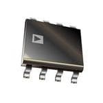
| 描述 | IC VREF SERIES PREC 10V 8-SOIC |
| 产品分类 | |
| 品牌 | Analog Devices Inc |
| 数据手册 | |
| 产品图片 |
|
| 产品型号 | AD587KRZ-REEL7 |
| rohs | 无铅 / 符合限制有害物质指令(RoHS)规范要求 |
| 产品系列 | - |
| 供应商器件封装 | 8-SOIC N |
| 其它名称 | AD587KRZ-REEL7DKR |
| 包装 | Digi-Reel® |
| 参考类型 | 串联,精度 |
| 安装类型 | 表面贴装 |
| 容差 | ±0.05% |
| 封装/外壳 | 8-SOIC(0.154",3.90mm 宽) |
| 工作温度 | 0°C ~ 70°C |
| 标准包装 | 1 |
| 温度系数 | 10ppm/°C |
| 电压-输入 | 13.5 V ~ 36 V |
| 电压-输出 | 10V |
| 电流-输出 | 10mA |
| 电流-阴极 | - |
| 电流-静态 | 4mA |
| 通道数 | 1 |


- 商务部:美国ITC正式对集成电路等产品启动337调查
- 曝三星4nm工艺存在良率问题 高通将骁龙8 Gen1或转产台积电
- 太阳诱电将投资9.5亿元在常州建新厂生产MLCC 预计2023年完工
- 英特尔发布欧洲新工厂建设计划 深化IDM 2.0 战略
- 台积电先进制程称霸业界 有大客户加持明年业绩稳了
- 达到5530亿美元!SIA预计今年全球半导体销售额将创下新高
- 英特尔拟将自动驾驶子公司Mobileye上市 估值或超500亿美元
- 三星加码芯片和SET,合并消费电子和移动部门,撤换高东真等 CEO
- 三星电子宣布重大人事变动 还合并消费电子和移动部门
- 海关总署:前11个月进口集成电路产品价值2.52万亿元 增长14.8%


PDF Datasheet 数据手册内容提取
High Precision 10 V Reference AD587 FEATURES FUNCTIONAL BLOCK DIAGRAM Laser trimmed to high accuracy +VIN REDNUOCISTEION 10.000 V ± 5 mV (U grade) 2 8 Trimmed temperature coefficient RS 5 ppm/°C maximum (U grade) Noise-reduction capability A1 6 VOUT Low quiescent current: 4 mA maximum RF Output trim capability RT MIL-STD-883-compliant versions available 5 TRIM RI AD587 4 GND NPPOIONITN1E,TPSI.NN3O,ACNODNNPEINCT7IAORNESITNOTETRHNEASLETPEOSINTTS. 00530-001 Figure 1. GENERAL DESCRIPTION PRODUCT HIGHLIGHTS The AD587 represents a major advance in state-of-the-art 1. Laser trimming of both initial accuracy and temperature monolithic voltage references. Using a proprietary ion- coefficients. This laser trimming results in very low errors implanted buried Zener diode and laser wafer trimming of high over temperature without the use of external components. stability thin-film resistors, the AD587 provides outstanding The AD587U guarantees ±14 mV maximum total error performance at low cost. between −55°C and +125°C. 2. Optional fine trim connection. This connection is designed The AD587 offers much higher performance than most other for applications requiring higher precision. 10 V references. Because the AD587 uses an industry-standard 3. Instant upgrade of any system using an industry-standard pinout, many systems can be upgraded instantly with the AD587. pinout 10 V reference. The buried Zener approach to reference design provides lower 4. Very low output noise. AD587 output noise is typically noise and drift than band gap voltage references. The AD587 4 μV p-p. A noise-reduction pin is provided for additional offers a noise-reduction pin that can be used to further reduce noise filtering using an external capacitor. the noise level generated by the buried Zener. 5. MIL-STD-883-compliant versions available. Refer to the The AD587 is recommended for use as a reference for 8-bit, Analog Devices Military/Aerospace Reference Manual for 10-bit, 12-bit, 14-bit, or 16-bit DACs that require an external detailed specifications. precision reference. The device is also ideal for successive approximation or integrating ADCs with up to 14 bits of accuracy. In general, it offers better performance than standard on-chip references. The AD587J and AD587K are specified for operation from 0°C to 70°C, and the AD587U is specified for operation from −55°C to +125°C. The AD587JQ and AD587UQ models are available in 8-lead CERDIP. Other models are available in an 8-lead SOIC package for surface-mount applications, or in an 8-lead PDIP. Rev. H Information furnished by Analog Devices is believed to be accurate and reliable. However, no responsibility is assumed by Analog Devices for its use, nor for any infringements of patents or other One Technology Way, P.O. Box 9106, Norwood, MA 02062-9106, U.S.A. rights of third parties that may result from its use. Specifications subject to change without notice. No license is granted by implication or otherwise under any patent or patent rights of Analog Devices. Tel: 781.329.4700 www.analog.com Trademarks and registered trademarks are the property of their respective owners. Fax: 781.461.3113 ©1998–2007 Analog Devices, Inc. All rights reserved.
AD587 TABLE OF CONTENTS Features..............................................................................................1 Noise Performance and Reduction.............................................6 Functional Block Diagram..............................................................1 Turn-On Time...............................................................................7 General Description.........................................................................1 Dynamic Performance..................................................................7 Product Highlights...........................................................................1 Load Regulation............................................................................8 Revision History...............................................................................2 Temperature Performance............................................................8 Specifications.....................................................................................3 Negative Reference Voltage from an AD587.............................9 Absolute Maximum Ratings............................................................4 Applications Information..............................................................10 ESD Caution..................................................................................4 Using the AD587 with Converters...........................................10 Pin Configuration and Function Descriptions.............................5 Outline Dimensions.......................................................................11 Theory of Operation........................................................................6 Ordering Guide..........................................................................12 Applying the AD587....................................................................6 REVISION HISTORY 9/07—Rev. G to Rev. H 7/04—Rev. E to Rev. F Deleted AD587L Grade.....................................................Universal Changes to Ordering Guide.............................................................3 Change to Product Highlights.........................................................1 7/03—Rev. D to Rev. E. Changes to the Negative Reference Voltage from an Deletion of S and T Grades...............................................Universal AD587 Section..............................................................................9 Edits to Ordering Guide...................................................................2 Changes to Figure 19.......................................................................10 Deletion of Die Specifications.........................................................3 Changes to Figure 21 and Figure 22..............................................10 Edits to Figure 3.................................................................................4 Updated Outline Dimensions........................................................11 Updated Outline Dimensions..........................................................9 Changes to Ordering Guide...........................................................12 4/05—Rev. F to Rev. G Updated Format..................................................................Universal Added Table 3.....................................................................................5 Updated Outline Dimensions........................................................11 Changes to Ordering Guide...........................................................13 Rev. H | Page 2 of 12
AD587 SPECIFICATIONS T = 25°C, V = 15 V, unless otherwise noted. A IN Table 1. AD587J AD587K AD587U Parameter Min Typ Max Min Typ Max Min Typ Max Unit OUTPUT VOLTAGE 9.990 10.010 9.995 10.005 9.995 10.005 V OUTPUT VOLTAGE DRIFT1 0°C to 70°C 20 10 5 ppm/°C −55°C to +125°C 20 10 5 ppm/°C GAIN ADJUSTMENT +3 +3 +3 % −1 −1 −1 % LINE REGULATION1 13.5 V ≤ +V ≤ 36 V IN T to T ±100 ±100 ±100 μV/V MIN MAX LOAD REGULATION1 Sourcing 0 mA < I < 10 mA OUT T to T ±100 ±100 ±100 μV/mA MIN MAX Sourcing −10 mA < I < 0 mA2 OUT T to T ±100 ±100 ±100 μV/mA MIN MAX QUIESCENT CURRENT 2 4 2 4 2 4 mA POWER DISSIPATION 30 30 30 mW OUTPUT NOISE 0.1 Hz to 10 Hz 4 4 4 μV p-p Spectral Density, 100 Hz 100 100 100 nV/√Hz LONG-TERM STABILITY ±15 ±15 ±15 ppm/1000 hr SHORT-CIRCUIT CURRENT-TO-GROUND 30 70 30 70 30 70 mA SHORT-CIRCUIT CURRENT-TO-+V 30 70 30 70 30 70 mA IN TEMPERATURE RANGE Specified Performance (J, K) 0 70 0 70 0 70 °C Operating Performance (J, K)3 −40 +85 −40 +85 −40 +85 °C Specified Performance (U) −55 +125 −55 +125 −55 +125 °C Operating Performance (U)3 −55 +125 −55 +125 −55 +125 °C 1 Specification is guaranteed for all packages and grades. CERDIP-packaged parts are 100% production tested. 2 Load regulation (sinking) specification for SOIC (R-8) package is ±200 μV/mA. 3 The operating temperature range is defined as the temperature extremes at which the device will still function. Parts may deviate from their specified performance outside their specified temperature range. Rev. H | Page 3 of 12
AD587 ABSOLUTE MAXIMUM RATINGS Table 2. Parameter Rating Stresses above those listed under Absolute Maximum Ratings +V to Ground 36 V may cause permanent damage to the device. This is a stress IN Power Dissipation (25°C) 500 mW rating only; functional operation of the device at these or any Storage Temperature Range −65°C to +150°C other conditions above those indicated in the operational Lead Temperature (Soldering, 10 sec) 300°C section of this specification is not implied. Exposure to absolute Package Thermal Resistance maximum rating conditions for extended periods may affect θJC 22°C/W device reliability. θJA 110°C/W ESD CAUTION Output Protection Short to Ground Indefinite1 Short to +V Momentary1 IN 1 Period for which output is safe. Rev. H | Page 4 of 12
AD587 PIN CONFIGURATION AND FUNCTION DESCRIPTIONS NOISE TP* 1 8 REDUCTION +VIN 2 AD587 7 TP* TOP VIEW TP* 3 (Not to Scale) 6 VOUT GND 4 5 TRIM * TTNPOO D TCEHONENOSNTEEE PCSITNFISOA.CNTSO SRHYO TUELSDT B PEO MINATD.E 00530-002 Figure 2. Pin Configuration Table 3. Pin Function Descriptions Pin No. Mnemonic Description 1, 3, 7 TP No Connection. Leave floating. 2 +V Input Voltage. IN 4 GND Ground. 5 TRIM Fine Trimming of Output Voltage. See Figure 4. 6 V Output Voltage. OUT 8 NOISE REDUCTION Noise Reduction of Output Voltage. Reduces noise via external capacitor to ground. Rev. H | Page 5 of 12
AD587 THEORY OF OPERATION The AD587 consists of a proprietary buried Zener diode NOISE PERFORMANCE AND REDUCTION reference, an amplifier to buffer the output, and several high Noise generated by the AD587 is typically less than 4 μV p-p stability thin-film resistors, as shown in Figure 3. This design over the 0.1 Hz to 10 Hz band. Noise in a 1 MHz bandwidth is results in a high precision monolithic 10 V output reference approximately 200 μV p-p. The dominant source of this noise is with initial offset of 5 mV or less. The temperature-compensa- the buried Zener, contributing approximately 100 nV/√Hz. By tion circuitry provides the device with a temperature coefficient comparison, the contribution of the op amp is negligible. of less than 5 ppm/°C. Figure 5 shows the 0.1 Hz to 10 Hz noise of a typical AD587. NOISE The noise measurement is made with a band-pass filter made +VIN REDUCTION 2 8 of a 1-pole high-pass filter with a corner frequency at 0.1 Hz and a 2-pole low-pass filter with a corner frequency at 12.6 Hz RS to create a filter with a 9.922 Hz bandwidth. A1 6 VOUT RF 1µV 5s RT 5 TRIM 100 90 RI AD587 4 1µV GND NPPIOONITN1ET,PSI.NN3O,ACNODNNPEINCT7IAORNESITNOTETRHNEASLETPEOSINTTS. 00530-003 Figure 3. Functional Block Diagram 10 0% A capacitor can be added at the NOISE REDUCTION pin (cPoinnt r8ib) utoti ofonr mof ath leo wZ-epnaesrs t foi ltthere wciirtchu RitS. to reduce the noise 00530-005 Figure 5. 0.1 Hz to 10 Hz Noise APPLYING THE AD587 If further noise reduction is desired, an external capacitor can The AD587 is simple to use in virtually all precision reference be added between the NOISE REDUCTION pin and ground, applications. When power is applied to Pin 2 and Pin 4 is as shown in Figure 4. This capacitor, combined with the 4 kΩ RS grounded, Pin 6 provides a 10 V output. No external compo- and the Zener resistances, forms a low-pass filter on the output nents are required; the degree of desired absolute accuracy is of the Zener cell. A 1 μF capacitor has a 3 dB point at 40 Hz achieved simply by selecting the required device grade. The and reduces the high frequency (up to 1 MHz) noise to about AD587 requires less than 4 mA quiescent current from an 160 μV p-p. Figure 6 shows the 1 MHz noise of a typical AD587, operating supply of 15 V. both with and without a 1 μF capacitor. Fine trimming may be desired to set the output level to exactly 200µV 50µs 10.000 V (calibrated to a main system reference). System cali- bration may also require a reference voltage that is slightly 100 different from 10.000 V, for example, 10.24 V for binary CN– 1µF 90 applications. In either case, the optional fine-trimming circuit shown in Figure 4 can offset the output by as much as 300 mV with minimal effect on other device characteristics. +VIN NO CN 10 0% 2 OPTIONAL RCEADPUANCCOTITIISOOENR- 8 NROEDISUECVTINIONVOUT 6 OUTPUT Figure 6. Effect of 1 μF Noise-Reduction Capacitor on Broadband No00530-006is e AD587 CN TRIM 5 10kΩ 1µF GND 4 00530-004 Figure 4. Optional Fine-Trimming Configuration Rev. H | Page 6 of 12
AD587 TURN-ON TIME 10V 1V 100ms Upon application of power (cold start), the time required for +VIN the output voltage to reach its final value within a specified 100 90 error band is defined as the turn-on settling time. Two compo- nents normally associated with this are the time for the active circuits to settle and the time for the thermal gradients on the chip to stabilize. Figure 7, Figure 8, and Figure 9 show the turn- on characteristics of the AD587. These figures show the settling VOUT 10 to be about 60 μs to 0.01%. Note the absence of any thermal tails 0% when the horizontal scale is expanded to 1 ms/cm in Figure 8. Output turn-on time is modified when an external noise reduc- 00530-009 tion capacitor is used. When present, this capacitor acts as an Figure 9. Turn-On with 1 μF CN additional load to the current source of the internal Zener DYNAMIC PERFORMANCE diode, resulting in a somewhat longer turn-on time. In the case The output buffer amplifier is designed to provide the AD587 of a 1 μF capacitor, the initial turn-on time is approximately 400 ms to 0.01%, as shown in Figure 9. with static and dynamic load regulation that is superior to less complete references. 10V 1mV Many ADCs and DACs present transient current loads to the +VIN reference, and poor reference response can degrade the con- 100 90 verter’s performance. Figure 11 and Figure 12 display the characteristics of the AD587 VOUT output amplifier driving a 0 mA to 10 mA load. 10 VOUT 0% 7.0V 1kΩ 20V Fi1g0uVre 7. Electrical Turn-On 1m20sµs 00530-007 Figure 10. TrAanDs5ie8n7t Load TVeLst Circu10it0V V 00530-010 +VIN 100 90 10V 50mV 1µs VOUT VL 100 90 10 VOUT 0% 00530-008 01%0 Figure 8. Extended Time Scale 00530-011 Figure 11. Large-Scale Transient Response Rev. H | Page 7 of 12
AD587 ΔVOUT (µV) 10V 1mV 2µs VL 100 1000 90 500 2 4 6 8 10 LOAD (mA) VOUT –6 –4 –2 0 –500 –1000 10 0% 00530-012 Figure 15. Typical Load Regulation Characteristics 00530-015 Figure 12. Fine-Scale Setting for Transient Load TEMPERATURE PERFORMANCE In some applications, a varying load may be both resistive and The AD587 is designed for precision reference applications capacitive in nature, or the load may be connected to the where temperature performance is critical. Extensive tempera- AD587 by a long capacitive cable. ture testing ensures that the device’s high level of performance is Figure 14 displays the output amplifier characteristics driving a maintained over the operating temperature range. 1000 pF, 0 mA to 10 mA load. Some confusion exists in the area of defining and specifying reference voltage error over temperature. Historically, references have been characterized using a maximum deviation per degree VOUT 7.0V CL Celsius, such as ppm/°C. However, because of nonlinearities in 1000pF 1kΩ temperature characteristics that originated in standard Zener references (such as S-type characteristics), most manufacturers VL 10V have begun to use a maximum limit error-band approach to AD587 0V 00530-013 sopuetpciufyt adte tvhirceees .o Trh miso treec htenmiqpueer aitnuvroelsv teos tshpee cmifeya asnu roeumtpeuntt of the Figure 13. Capacitive Load Transient/Response Test Circuit voltage error band. 10V 200mV 1µs CL = 0 100 90 CL = 1000pF 10 0% VL 00530-014 Figure 14. Output Response with Capacitive Load LOAD REGULATION The AD587 has excellent load regulation characteristics. Figure 15 shows that varying the load several milliamperes changes the output by only a few microvolts. Rev. H | Page 8 of 12
AD587 Each AD587J and AD587K grade unit is tested at 0°C, 25°C, NEGATIVE REFERENCE VOLTAGE FROM AN AD587 and 70°C. Each AD587U grade unit is tested at −55°C, +25°C, The AD587 can be used as shown in Figure 17 to provide a and +125°C. This approach ensures that the variations of the precision −10.000 V output. The +V pin is tied to at least a IN output voltage that occur as the temperature changes within the +3.5 V supply, the output pin is grounded, and the AD587 specified range are contained within a box whose diagonal has a ground pin is connected through a resistor (R) to a −15 V S slope equal to the maximum specified drift. The position of the supply. The −10 V output is taken from the ground pin (Pin 4) box on the vertical scale changes from device to device as initial instead of V . It is essential to arrange the output load and the OUT error and the shape of the curve vary. The maximum height of supply resistor (R) so that the net current through the AD587 is S the box for the appropriate temperature range and device grade between 2.5 mA and 10.0 mA (R should be kept below 1 kΩ). S is shown in Figure 16. Duplication of these results requires a The temperature characteristics and long-term stability of the combination of high accuracy and stable temperature control in device is essentially the same as that of a unit used in the a test system. standard 10 V output configuration. DEVICE MAXIMUM OUTPUT CHANGE – mV 3.5V→26V GRADE 0TO +70°C –55°CTO +125°C AD587J 14.00 2 AAFDDig55u88r77eKU 16. Maxim7u.0m0 Output Chang9e.0 i0n Millivolt00530-017s +VINVOUT 6 AD587 GND 4 ←IL –10V 1nF –15VRS 2.5mA <R5VS– IL < 10mA 00530-018 Figure 17. AD587 as a Negative 10 V Reference Rev. H | Page 9 of 12
AD587 APPLICATIONS INFORMATION USING THE AD587 WITH CONVERTERS +VIN The AD587 is an ideal reference for a variety of 8-bit, 12-bit, 2 14-bit, and 16-bit ADCs and DACs. Several examples follow. +VIN 10 V Reference with Multiplying CMOS DACs or ADCs AD58V7OUT 6 RC IL = 1R 0 CV + IBIAS 500Ω The AD587 is ideal for applications with 10-bit and 12-bit MIN GND mFiguultripe l1y8in, gth Ce MADO5S8 D7 AisC psa. iIrne dth we isttha nthdea rAdD h7o5o4k5u 1p2, -sbhiot wmnu ilnti - 4 00530-021 plying DAC and the AD711 high speed BiFET op amp. The Figure 20. Precision Current Source amplifier DAC configuration produces a unipolar 0 V to −10 V Precision High Current Supply output range. Bipolar output applications and other operating For higher currents, the AD587 can easily be connected to a details can be found in the individual product data sheets. power PNP or power Darlington PNP device. The circuits in +15V Figure 21 and Figure 22 can deliver up to 4 A to the load. The +15V R2 0.1µF C1 +15V 0.1 μF capacitor is required only if the load has a significant +VIN 33pF 0.1µF capacitive component. If the load is purely resistive, improved AD587 VDD RFB high frequency supply rejection results can be obtained by VOUT VREF OUT1 removing the capacitor. AD711 VOUT TRIM 10kΩ AD7545 AGND 0VTO –10V +VIN GND DGND 0.1µF DB11TO DB0 –15V 00530-019 220Ω Figure 18. Low Power 12-Bit CMOS DAC Application 2N6285 The AD587 can also be used as a precision reference for multi- ple DACs. Figure 19 shows the AD587, the AD7628 dual DAC, and the AD712 dual op amp hooked up for single-supply 0.1µF operation to produce 0 V to −10 V outputs. Because both DACs are on the same die and share a common reference and output 2 op amps, the DAC outputs will exhibit similar gain temperature +VIN co+e1f5fVicients (TCs). AD587 VOUT 6 RC IL = 1R 0 CV + IBIAS +15V GND +VIN 0.1µF RFB A 4 00530-022 VREFA OUT A Figure 21. Precision High Current Source VOUT DACA AGDN5D87 INPDUATTAS DDBB07 AD7628 RAFGBN DB AD712 V0OTUOT A–1 =0V +VIN 220Ω OUT B 18 VREFB DACB 2N6285 VOUTB = DGND 0TO –10V 00530-020 0.1µF Figure 19. AD587 as a 10 V Reference for a CMOS Dual DAC Precision Current Source 2 The design of the AD587 allows it to be easily configured as a cur- +VIN srehnotw snou irnc eF.i Bguy rceh 2o0o,s itnhge tuhsee cr ocnatnr ovla rreys itshtoer l (oRaCd) cvuiar rthene te fqruoamtio tnh e AD587 VOUT 6 +V1O0UVT @ 4A quiescent current (2 mA typically) to approximately 10 mA. GND 4 00530-023 Figure 22. Precision High Current Voltage Source Rev. H | Page 10 of 12
AD587 OUTLINE DIMENSIONS 0.005 (0.13) 0.055 (1.40) MIN MAX 8 5 5.00(0.1968) 0.310 (7.87) 4.80(0.1890) 0.220 (5.59) 1 4 8 5 4.00 (0.1574) 6.20 (0.2441) 3.80 (0.1497) 1 4 5.80 (0.2284) 0.100 (2.54) BSC 0.405 (10.29) MAX 0.320 (8.13) 0.290 (7.37) 1.27 B(0S.C0500) 1.75 (0.0688) 00..5205 ((00..00109969)) 45° 0.200 (5M.0A8X) 00..006105 ((10..5328)) 0.25 (0.0098) 1.35 (0.0532) 8° 0.10 (0.0040) 0° 0.200 (5.08) 0.150 (3.81) MIN COPLANARITY 0.51 (0.0201) 0.125 (3.18) 0.10 SEPALTAINNGE 0.31 (0.0122) 00..2157 ((00..00009687)) 10..2470 ((00..00510507)) 00..002134 ((00..5386)) 0.070 (1.78) SPELAANTIENG 1 05°° 00..001058 ((00..3280)) 0.030 (0.76) COMPLIANTTO JEDEC STANDARDS MS-012-AA C(RINOEFNPEATRRREOENNLCLTEIHN EOGSN EDLSIYM)AEANNRDSEI AORRNOESU NANORDEET DAIN-PO MPFRIFLO LMPIIMRLELIATIMTEEER TFSEO; RIRN ECUQHSU EDI VIINMA LEDENENSSTIIOGSN NFS.OR 012407-A C(RINOE FNPETARRREOENLNCLTEIHN EOGSN DELISYM) E AANNRSDEI O ARNROSEU ANNRDOEET D IAN-PO IPNFRFC OHINPECRSH;IA METIQELU LFIIOMVAREL TUEESNRET D SINI MF DEOENRSSIIGONN.S Figure 23. 8-Lead Standard Small Outline Package [SOIC_N] Figure 25. 8-Lead Ceramic Dual In-Line Package [CERDIP] Narrow Body (R-8) (Q-8) Dimensions shown in millimeters and (inches) Dimensions shown in inches and (millimeters) 0.400 (10.16) 0.365 (9.27) 0.355 (9.02) 8 5 0.280 (7.11) 0.250 (6.35) 1 4 0.240 (6.10) 0.325 (8.26) 0.310 (7.87) 0.100 (2.54) 0.300 (7.62) BSC 0.060 (1.52) 0.195 (4.95) 0.210 (5.33) MAX 0.130 (3.30) MAX 0.115 (2.92) 0.015 0.150 (3.81) (0.38) 0.015 (0.38) 0.130 (3.30) MIN GAUGE 0.115 (2.92) SPLEAATNIENG PLANE 00..001140 ((00..3265)) 00..002128 ((00..5466)) 0M.0IN05 (0.13) 0.43M0 A(1X0.92) 0.008 (0.20) 0.014 (0.36) 0.070 (1.78) 0.060 (1.52) 0.045 (1.14) COMPLIANTTO JEDEC STANDARDS MS-001 CONTROLLING DIMENSIONSARE IN INCHES; MILLIMETER DIMENSIONS (RCINEOFRPEANRREERENN LCTEEHA EODSNSEL MSY)AAAYNR BDEE AR CROOEU NNNFODIGETUDAR-POEPFDRFOA INSPC RWHIAH ETOEQL UFEIO VORAR LU EHSNAETL ISFN FLDOEEARSDIGSN.. 070606-A Figure 24. 8-Lead Plastic Dual In-Line Package [PDIP] Narrow Body (N-8) Dimensions shown in inches and (millimeters) Rev. H | Page 11 of 12
AD587 ORDERING GUIDE Model Initial Error Temperature Coefficient Temperature Range Package Description Package Option AD587JQ 10 mV 20 ppm/°C 0°C to 70°C 8-Lead CERDIP Q-8 AD587JR 10 mV 20 ppm/°C 0°C to 70°C 8-Lead SOIC_N R-8 AD587JR-REEL 10 mV 20 ppm/°C 0°C to 70°C 8-Lead SOIC_N R-8 AD587JR-REEL7 10 mV 20 ppm/°C 0°C to 70°C 8-Lead SOIC_N R-8 AD587JRZ1 10 mV 20 ppm/°C 0°C to 70°C 8-Lead SOIC_N R-8 AD587JRZ-REEL1 10 mV 20 ppm/°C 0°C to 70°C 8-Lead SOIC_N R-8 AD587JRZ-REEL71 10 mV 20 ppm/°C 0°C to 70°C 8-Lead SOIC_N R-8 AD587JN 10 mV 20 ppm/°C 0°C to 70°C 8-Lead PDIP N-8 AD587JNZ1 10 mV 20 ppm/°C 0°C to 70°C 8-Lead PDIP N-8 AD587KR 5 mV 10 ppm/°C 0°C to 70°C 8-Lead SOIC_N R-8 AD587KR-REEL 5 mV 10 ppm/°C 0°C to 70°C 8-Lead SOIC_N R-8 AD587KR-REEL7 5 mV 10 ppm/°C 0°C to 70°C 8-Lead SOIC_N R-8 AD587KRZ1 5 mV 10 ppm/°C 0°C to 70°C 8-Lead SOIC_N R-8 AD587KRZ-REEL1 5 mV 10 ppm/°C 0°C to 70°C 8-Lead SOIC_N R-8 AD587KRZ-REEL71 5 mV 10 ppm/°C 0°C to 70°C 8-Lead SOIC_N R-8 AD587KN 5 mV 10 ppm/°C 0°C to 70°C 8-Lead PDIP N-8 AD587KNZ1 5 mV 10 ppm/°C 0°C to 70°C 8-Lead PDIP N-8 AD587UQ 5 mV 5 ppm/°C −55°C to +125°C 8-Lead CERDIP Q-8 1 Z = RoHS Compliant Part. ©1998–2007 Analog Devices, Inc. All rights reserved. Trademarks and registered trademarks are the property of their respective owners. C00530-0-9/07(H) Rev. H | Page 12 of 12
Mouser Electronics Authorized Distributor Click to View Pricing, Inventory, Delivery & Lifecycle Information: A nalog Devices Inc.: AD587JRZ 5962-8982502PA AD587UQ AD587KRZ AD587KNZ AD587KRZ-REEL AD587KRZ-REEL7 AD587JQ AD587JRZ-REEL7 AD587JRZ-REEL 5962-8982503PA AD587JNZ