 Datasheet下载
- 型号: TLV320AIC3254IRHBR
- 制造商: Texas Instruments
- 库位|库存: xxxx|xxxx
- 要求:
| 数量阶梯 | 香港交货 | 国内含税 |
| +xxxx | $xxxx | ¥xxxx |
查看当月历史价格
查看今年历史价格
TLV320AIC3254IRHBR产品简介:
ICGOO电子元器件商城为您提供TLV320AIC3254IRHBR由Texas Instruments设计生产,在icgoo商城现货销售,并且可以通过原厂、代理商等渠道进行代购。 TLV320AIC3254IRHBR价格参考¥询价-¥询价。Texas InstrumentsTLV320AIC3254IRHBR封装/规格:接口 - 编解码器, Stereo Audio Interface 32 b Serial 32-VQFN (5x5)。您可以下载TLV320AIC3254IRHBR参考资料、Datasheet数据手册功能说明书,资料中有TLV320AIC3254IRHBR 详细功能的应用电路图电压和使用方法及教程。
TLV320AIC3254IRHBR是德州仪器(Texas Instruments)推出的一款高性能音频编解码器,广泛应用于便携式音频设备中。其主要应用场景包括智能手机、平板电脑、便携式媒体播放器、语音录音设备及蓝牙音频适配器等。该器件集成了立体声ADC和DAC,支持高保真音频录制与回放,具备低功耗特性,非常适合电池供电的移动设备。

TLV320AIC3254IRHBR支持多种数字音频接口(如I²S、SPI),可灵活连接应用处理器或DSP,同时提供丰富的模拟输入输出选项,可用于连接麦克风、耳机、扬声器等。其内置的迷你DSP还可用于实现音频预处理功能,如滤波、混音和增益控制,适用于语音增强、噪声抑制等场景。

此外,该芯片还广泛用于工业手持设备、医疗音频设备(如便携式听诊器)以及需要高质量语音采集与播放的物联网终端。凭借小封装(RHBT,36引脚VQFN)和高集成度,TLV320AIC3254IRHBR在空间受限的设计中具有显著优势,是高性能、低功耗音频系统的理想选择。
| 参数 | 数值 |
| ADC/DAC数 | 2 / 2 |
| ADC数量 | 2 |
| 产品目录 | 集成电路 (IC)半导体 |
| DAC数量 | 2 |
| 描述 | IC STEREO AUDIO CODEC 1.8V 32QFN接口—CODEC Very LW PWR Stereo Audio CODEC/miniDSP |
| 产品分类 | |
| 品牌 | Texas Instruments |
| 产品手册 | http://www.ti.com/lit/gpn/tlv320aic3254 |
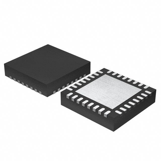
| 产品图片 |
|
| rohs | 符合RoHS无铅 / 符合限制有害物质指令(RoHS)规范要求 |
| 产品系列 | 接口 IC,接口—CODEC,Texas Instruments TLV320AIC3254IRHBR- |
| 数据手册 | |
| 产品型号 | TLV320AIC3254IRHBR |
| THD+噪声 | - 85 dB ADC/- 83 dB DAC |
| 三角积分 | 是 |
| 产品培训模块 | http://www.digikey.cn/PTM/IndividualPTM.page?site=cn&lang=zhs&ptm=25729 |
| 产品目录页面 | |
| 产品种类 | 接口—CODEC |
| 供应商器件封装 | 32-VQFN(5x5) |
| 信噪比 | 93 dB ADC/100 dB DAC |
| 信噪比,ADC/DAC(db)(典型值) | 93 / 100 |
| 其它名称 | 296-23776-6 |
| 分辨率 | 32 bit |
| 分辨率(位) | 32 b |
| 制造商产品页 | http://www.ti.com/general/docs/suppproductinfo.tsp?distId=10&orderablePartNumber=TLV320AIC3254IRHBR |
| 动态范围,ADC/DAC(db)(典型值) | 93 / 100 |
| 包装 | Digi-Reel® |
| 单位重量 | 71.800 mg |
| 商标 | Texas Instruments |
| 安装类型 | 表面贴装 |
| 安装风格 | SMD/SMT |
| 封装 | Reel |
| 封装/外壳 | 32-VFQFN 裸露焊盘 |
| 封装/箱体 | VQFN-32 |
| 工作温度 | -40°C ~ 85°C |
| 工厂包装数量 | 3000 |
| 接口类型 | Serial (I2C, SPI) |
| 数据接口 | 串行 |
| 最大工作温度 | + 85 C |
| 最小工作温度 | - 40 C |
| 标准包装 | 1 |
| 特色产品 | http://www.digikey.com/cn/zh/ph/texas-instruments/TLV320AIC.html |
| 电压-电源,数字 | 1.26 V ~ 1.95 V |
| 电压-电源,模拟 | 1.9 V ~ 3.6 V |
| 类型 | 立体声音频 |
| 系列 | TLV320AIC3254 |
| 转换速率 | 192 kHz |


- 商务部:美国ITC正式对集成电路等产品启动337调查
- 曝三星4nm工艺存在良率问题 高通将骁龙8 Gen1或转产台积电
- 太阳诱电将投资9.5亿元在常州建新厂生产MLCC 预计2023年完工
- 英特尔发布欧洲新工厂建设计划 深化IDM 2.0 战略
- 台积电先进制程称霸业界 有大客户加持明年业绩稳了
- 达到5530亿美元!SIA预计今年全球半导体销售额将创下新高
- 英特尔拟将自动驾驶子公司Mobileye上市 估值或超500亿美元
- 三星加码芯片和SET,合并消费电子和移动部门,撤换高东真等 CEO
- 三星电子宣布重大人事变动 还合并消费电子和移动部门
- 海关总署:前11个月进口集成电路产品价值2.52万亿元 增长14.8%


PDF Datasheet 数据手册内容提取
Product Sample & Technical Tools & Support & Folder Buy Documents Software Community TLV320AIC3254 SLAS549D–SEPTEMBER2008–REVISEDNOVEMBER2014 TLV320AIC3254 Ultra Low Power Stereo Audio Codec with Embedded miniDSP 1 Features 2 Applications • StereoAudioDACwith100dBSNR • PortableNavigationDevices(PND) 1 • 4.1mWStereo48ksps DACPlayback • PortableMediaPlayer(PMP) • StereoAudioADCwith93dBSNR • MobileHandsets • 6.1-mWStereo48-kspsADCRecord • Communication • PowerTune™ • PortableComputing • ExtensiveSignalProcessingOptions • AdvancedDSPalgorithms • EmbeddedminiDSP 3 Description • SixSingle-EndedorThreeFully-Differential The TLV320AIC3254 (sometimes referred to as the AnalogInputs AIC3254) is a flexible, low-power, low-voltage stereo • StereoAnalogandDigitalMicrophoneInputs audio codec with programmable inputs and outputs, • StereoHeadphoneOutputs PowerTune capabilities, fully-programmable miniDSP, • StereoLineOutputs fixed predefined and parameterizable signal processing blocks, integrated PLL, integrated LDOs • VeryLow-NoisePGA andflexibledigitalinterfaces. • LowPowerAnalogBypassMode • ProgrammableMicrophoneBias DeviceInformation(1) • ProgrammablePLL PARTNUMBER PACKAGE BODYSIZE(NOM) • IntegratedLDO TLV320AIC3254 VQFN(32) 5.00mmx5.00mm • 5mmx5mm32-pinQFNPackage (1) For all available packages, see the orderable addendum at theendofthedatasheet. 4 Simplified Block Diagram IN1_L IN2_L AGC DRC Vol.Ctrl -72...0dB -6...+29dB IN3_L ++ 0…+47.5dB ALDeCft tpl ´ SPAirgDonCca.l SPDigrAonCca.l ´ LDeAfCt + 1dB steps HPL 0.5dB GainAdj. steps -30...0dB -6...+29dB + LOL Data 1dB steps -30...0dB miniDSP Interface miniDSP -6...+29dB + LOR 0… 1dB steps IN3_R ++ +47.5dB RAiDghCt tprGain´Adj. SPAirgDonCca.l SPDigrAonCca.l ´ RDiAgCht + -6...+29dB HPR 0.5dB steps IN2_R AGC DRC Vol.Ctrl -72...0dB 1dB steps IN1_R SPI_SReelescett CoSnPtrIo/l IB2Clock PLL DMigiict.al IntCertrrulpt SeIc2oSn IdFary I2SP Irnimtearfrayce HPVdd MicBias Mic ALDO Bias Supplies Pin Muxing/ClockRouting Ref Ref DLDO LDOin LDOSelect AVdd DVdd IOVdd AVss DVss IOVss SCL/SSZ SDA/MOSI MISO SCLK MCLK GPIO DOUT DIN BCLK WCLK 1 An IMPORTANT NOTICE at the end of this data sheet addresses availability, warranty, changes, use in safety-critical applications, intellectualpropertymattersandotherimportantdisclaimers.PRODUCTIONDATA.
TLV320AIC3254 SLAS549D–SEPTEMBER2008–REVISEDNOVEMBER2014 www.ti.com Table of Contents 1 Features.................................................................. 1 8.17 I2CInterfaceTiming..............................................20 2 Applications........................................................... 1 8.18 SPIInterfaceTiming(SeeFigure7).....................21 3 Description............................................................. 1 8.19 TypicalCharacteristics..........................................22 8.20 TypicalCharacteristics,FFT.................................24 4 SimplifiedBlockDiagram..................................... 1 9 ParameterMeasurementInformation................25 5 RevisionHistory..................................................... 2 10 DetailedDescription........................................... 25 6 DeviceComparisonTable..................................... 3 10.1 Overview...............................................................25 7 PinConfigurationandFunctions......................... 4 10.2 FunctionalBlockDiagram.....................................26 8 Specifications......................................................... 7 10.3 FeatureDescription...............................................26 8.1 AbsoluteMaximumRatings......................................7 10.4 DeviceFunctionalModes......................................34 8.2 HandlingRatings......................................................7 10.5 Software................................................................34 8.3 RecommendedOperatingConditions.......................7 10.6 RegisterMap.........................................................34 8.4 ThermalInformation..................................................8 11 ApplicationsandImplementation...................... 39 8.5 ElectricalCharacteristics,ADC.................................8 11.1 ApplicationInformation..........................................39 8.6 ElectricalCharacteristics,BypassOutputs.............10 11.2 TypicalApplication................................................39 8.7 ElectricalCharacteristics,MicrophoneInterface.....11 12 PowerSupplyRecommendations..................... 43 8.8 ElectricalCharacteristics,AudioDACOutputs.......12 13 Layout................................................................... 43 8.9 ElectricalCharacteristics,LDO...............................14 8.10 ElectricalCharacteristics,Misc.............................15 13.1 LayoutGuidelines.................................................43 8.11 ElectricalCharacteristics,LogicLevels.................16 13.2 LayoutExample....................................................44 8.12 I2SLJFandRJFTiminginMasterMode(see 14 DeviceandDocumentationSupport................. 45 Figure1)...................................................................16 14.1 DocumentationSupport........................................45 8.13 I2SLJFandRJFTiminginSlaveMode(see 14.2 Trademarks...........................................................45 Figure2)...................................................................17 14.3 ElectrostaticDischargeCaution............................45 8.14 DSPTiminginMasterMode(seeFigure3).........18 14.4 Glossary................................................................45 8.15 DSPTiminginSlaveMode(seeFigure4)...........19 15 Mechanical,Packaging,andOrderable 8.16 DigitalMicrophonePDMTiming(seeFigure5)....19 Information........................................................... 45 5 Revision History NOTE:Pagenumbersforpreviousrevisionsmaydifferfrompagenumbersinthecurrentversion. ChangesfromRevisionC(December2013)toRevisionD Page • AddedPinConfigurationandFunctionssection,HandlingRatingtable,FeatureDescriptionsection,Device FunctionalModes,ApplicationandImplementationsection,PowerSupplyRecommendationssection,Layout section,DeviceandDocumentationSupportsection,andMechanical,Packaging,andOrderableInformation section ................................................................................................................................................................................... 1 • Added"Audioinputmaxacsignalswing"totheRecommendedOperatingConditionstable............................................... 7 • AddedtheDigitalMicrophonePDMTiming(seeFigure5)section..................................................................................... 19 ChangesfromRevisionB(August2012)toRevisionC Page • Deleted"AcousticEchoCancellation(AEC)"and"ActiveNoiseCancellation(ANC)"fromapplicationslist.........................1 • ChangedthepindescriptionFrom:connecttoDVss.To:D-LDOenablesignal................................................................... 6 • Added"DVDD"toLDOsdisabledinoperatingconditionsstatement..................................................................................... 7 • Correctedt tot ............................................................................................................................................................. 21 hi h(DIN) 2 SubmitDocumentationFeedback Copyright©2008–2014,TexasInstrumentsIncorporated ProductFolderLinks:TLV320AIC3254
TLV320AIC3254 www.ti.com SLAS549D–SEPTEMBER2008–REVISEDNOVEMBER2014 6 Device Comparison Table ORDERNUMBER DESCRIPTION TLV320AIC3254 LowpowerstereoaudiocodecwithminiDSP. TLV320AIC3204 SameasTLV320AIC3204butwithoutminiDSP. TLV320AIC3256 SimilartoTLV320AIC3254butwithgroundcenteredheadphoneoutput. TLV320AIC3206 SameasTLV320AIC3256butwithoutminiDSP. Copyright©2008–2014,TexasInstrumentsIncorporated SubmitDocumentationFeedback 3 ProductFolderLinks:TLV320AIC3254
TLV320AIC3254 SLAS549D–SEPTEMBER2008–REVISEDNOVEMBER2014 www.ti.com 7 Pin Configuration and Functions This document describes signals that take on different names depending on how they are configured. In such cases, the different names are placed together and separated by slash (/) characters. For example, "SCL/SS". Activelowsignalsarerepresentedby overbars. RHBPackage (BottomView) 2 3 P P FP1 MF MF K K K M T/ D S K/ CL CL CL N/ OU VDVS CL M B W DI D O O S I I 1 8 GPIO/MFP5 32 9 SCL/SS RESET SDA/MOSI LDO_SELECT MISO/MFP4 DV SPI_SELECT DD DV IN1_L SS HPR IN1_R LDOIN IN2_L HPL 25 16 IN2_R 24 17 D R L R L S F S AVD LO LO N3_ N3_ BIA RE AVS I I C MI PinFunctions PIN NAME TYPE(1) DESCRIPTION 1 MCLK DI MasterClockInput 2 BCLK DIO Audioserialdatabus(primary)bitclock 3 WCLK DIO Audioserialdatabus(primary)wordclock Primaryfunction: Audioserialdatabusdatainput Secondaryfunction: 4 DIN/MFP1 DI DigitalMicrophoneInput GeneralPurposeClockInput GeneralPurposeInput Primaryfunction: Audioserialdatabusdataoutput Secondaryfunction: GeneralPurposeOutput 5 DOUT/MFP2 DO ClockOutput INT1Output INT2Output Audioserialdatabus(secondary)bitclockoutput Audioserialdatabus(secondary)wordclockoutput 6 IOV Power IOvoltagesupply1.1V–3.6V DD 7 IOV Ground IOgroundsupply SS (1) DI(DigitalInput),DO(DigitalOutput),DIO(DigitalInput/Output),AI(AnalogInput),AO(AnalogOutput),AIO(AnalogInput/Output) 4 SubmitDocumentationFeedback Copyright©2008–2014,TexasInstrumentsIncorporated ProductFolderLinks:TLV320AIC3254
TLV320AIC3254 www.ti.com SLAS549D–SEPTEMBER2008–REVISEDNOVEMBER2014 PinFunctions(continued) PIN NAME TYPE(1) DESCRIPTION Primaryfunction:(SPI_Select=1) SPIserialclock Secondaryfunction:(SPI_Select=0) Headphone-detectinput 8 SCLK/MFP3 DI Digitalmicrophoneinput Audioserialdatabus(secondary)bitclockinput Audioserialdatabus(secondary)DACorcommonwordclockinput Audioserialdatabus(secondary)ADCwordclockinput Audioserialdatabus(secondary)datainput GeneralPurposeInput I2Cinterfaceserialclock(SPI_Select=0) 9 SCL/SS DI SPIinterfacemodechip-selectsignal(SPI_Select=1) I2Cinterfacemodeserialdatainput(SPI_Select=0) 10 SDA/MOSI DI SPIinterfacemodeserialdatainput(SPI_Select=1) Primaryfunction:(SPI_Select=1) Serialdataoutput Secondaryfunction:(SPI_Select=0) Generalpurposeoutput CLKOUToutput 11 MISO/MFP4 DO INT1output INT2output Audioserialdatabus(primary)ADCwordclockoutput Digitalmicrophoneclockoutput Audioserialdatabus(secondary)dataoutput Audioserialdatabus(secondary)bitclockoutput Audioserialdatabus(secondary)wordclockoutput 12 SPI_SELECT DI Controlmodeselectpin(1=SPI,0=I2C) MultifunctionAnalogInput, 13 IN1_L AI orSingle-endedconfiguration:MIC1orLine1left orDifferentialconfiguration:MICorLineright,negative MultifunctionAnalogInput, 14 IN1_R AI orSingle-endedconfiguration:MIC1orLine1right orDifferentialconfiguration:MICorLineright,positive MultifunctionAnalogInput, 15 IN2_L AI orSingle-endedconfiguration:MIC2orLine2left orDifferentialconfiguration:MICorLineleft,positive MultifunctionAnalogInput, 16 IN2_R AI orSingle-endedconfiguration:MIC2orLine2right orDifferentialconfiguration:MICorLineleft,negative 17 AV Ground Analoggroundsupply SS 18 REF AO Referencevoltageoutputforfiltering 19 MICBIAS AO Microphonebiasvoltageoutput MultifunctionAnalogInput, orSingle-endedconfiguration:MIC3orLine3left, 20 IN3_L AI orDifferentialconfiguration:MICorLineleft,positive, orDifferentialconfiguration:MICorLineright,negative MultifunctionAnalogInput, orSingle-endedconfiguration:MIC3orLine3right, 21 IN3_R AI orDifferentialconfiguration:MICorLineleft,negative, orDifferentialconfiguration:MICorLineright,positive 22 LOL AO Leftlineoutput 23 LOR AO Rightlineoutput Analogvoltagesupply1.5V–1.95V 24 AV InputwhenA-LDOdisabled, DD Power FilteringoutputwhenA-LDOenabled Copyright©2008–2014,TexasInstrumentsIncorporated SubmitDocumentationFeedback 5 ProductFolderLinks:TLV320AIC3254
TLV320AIC3254 SLAS549D–SEPTEMBER2008–REVISEDNOVEMBER2014 www.ti.com PinFunctions(continued) PIN NAME TYPE(1) DESCRIPTION 25 HPL AO Lefthighpoweroutputdriver 26 LDOIN/ Power LDOInputsupplyandHeadphonePowersupply1.9V–3.6V HPVDD 27 HPR AO Righthighpoweroutputdriver 28 DV Ground DigitalGroundandChip-substrate SS IfLDO_SELECTPin=0(D-LDOdisabled) Digitalvoltagesupply1.26V–1.95V 29 DV Power DD IfLDO_SELECTPin=1(D-LDOenabled) Digitalvoltagesupplyfilteringoutput 30 LDO_SELECT DI D-LDOenablesignal(1=D-LDOenable,0=D-LDOdisabled) 31 RESET DI Reset(activelow) Primaryfunction: GeneralPurposedigitalIO Secondaryfunction: CLKOUTOutput 32 GPIO/MFP5 DI INT1Output INT2Output AudioserialdatabusADCwordclockoutput Audioserialdatabus(secondary)bitclockoutput Audioserialdatabus(secondary)wordclockoutput Digitalmicrophoneclockoutput ThermalPad ThermalPad N/A ConnecttoPCBgroundplane.Notinternallyconnected. 6 SubmitDocumentationFeedback Copyright©2008–2014,TexasInstrumentsIncorporated ProductFolderLinks:TLV320AIC3254
TLV320AIC3254 www.ti.com SLAS549D–SEPTEMBER2008–REVISEDNOVEMBER2014 8 Specifications 8.1 Absolute Maximum Ratings overoperatingfree-airtemperaturerange(unlessotherwisenoted) (1) MIN MAX UNIT AV toAV –0.3 2.2 V DD SS DV toDV –0.3 2.2 V DD SS Inputvoltage IOV toIOV –0.3 3.9 V DD SS LDOINtoAV –0.3 3.9 V SS DigitalInputvoltagetoground –0.3 IOV +0.3 V DD Analoginputvoltagetoground –0.3 AV +0.3 V DD Operatingtemperaturerange –40 85 °C Junctiontemperature(T Max) 105 °C J (1) Stressesbeyondthoselistedunder“absolutemaximumratings”maycausepermanentdamagetothedevice.Thesearestressratings only,andfunctionaloperationofthedeviceattheseoranyotherconditionsbeyondthoseindicatedunder“recommendedoperating conditions”isnotimplied.Exposuretoabsolute-maximum-ratedconditionsforextendedperiodsmayaffectdevicereliability. 8.2 Handling Ratings MIN MAX UNIT T Storagetemperaturerange –55 125 °C stg Humanbodymodel(HBM),perANSI/ESDA/JEDECJS-001,allpins(1) –2 2 kV Electrostatic V(ESD) discharge Cpihnasr(g2)eddevicemodel(CDM),perJEDECspecificationJESD22-C101,all –750 750 V (1) JEDECdocumentJEP155statesthat500-VHBMallowssafemanufacturingwithastandardESDcontrolprocess. (2) JEDECdocumentJEP157statesthat250-VCDMallowssafemanufacturingwithastandardESDcontrolprocess. 8.3 Recommended Operating Conditions MIN NOM MAX UNIT LDOIN 1.9 3.6 ReferencedtoAVSS(1) AVDD 1.5 1.8 1.95 PowerSupplyVoltageRange V IOVDD ReferencedtoIOVSS(1) 1.1 3.6 DVDD(2) ReferencedtoDVSS(1) 1.26 1.8 1.95 Clockdividerusesfractionaldivide (D>0),P=1,DVDD≥1.65V(Refertothetablein 10 20 MHz SLAA408,MaximumTLV320AIC3254ClockFrequencies) PLLInputFrequency Clockdividerusesintegerdivide (D=0),P=1,DVDD≥1.65V(Refertothetablein 0.512 20 MHz SLAA408,MaximumTLV320AIC3254ClockFrequencies) MCLK;MasterClockFrequency;DVDD≥1.65V 50 MCLK MasterClockFrequency MHz MCLK;MasterClockFrequency;DVDD≥1.26V 25 SCL SCLClockFrequency 400 kHz 0.75or Audioinputmaxacsignalswing CM=0.75V 0 0.530 AVDD-0.75(3) Vpeak (IN1_L,IN1_R,IN2_L,IN2_R,IN3_L, IN3_R) CM=0.9V 0 0.707 AVDD-00..99o(3r) Vpeak LOL,LOR Stereolineoutputloadresistance 0.6 10 kΩ Stereoheadphoneoutputloadresistance Single-endedconfiguration 14.4 16 Ω HPL,HPR Headphoneoutputloadresistance Differentialconfiguration 24.4 32 Ω CLout Digitaloutputloadcapacitance 10 pF TOPR OperatingTemperatureRange –40 85 °C (1) Allgroundsonboardaretiedtogethertopreventvoltagedifferencesofmorethan0.2Vmaximumforanycombinationofgroundsignals. (2) AtDV valueslowerthan1.65V,thePLLdoesnotfunction.RefertotheMaximumTLV320AIC3254ClockFrequenciestableinthe DD TLV320AIC3254ApplicationReferenceGuide(SLAA408)fordetailsonmaximumclockfrequencies. (3) Whicheverissmaller. Copyright©2008–2014,TexasInstrumentsIncorporated SubmitDocumentationFeedback 7 ProductFolderLinks:TLV320AIC3254
TLV320AIC3254 SLAS549D–SEPTEMBER2008–REVISEDNOVEMBER2014 www.ti.com 8.4 Thermal Information TLV320AIC3254 THERMALMETRIC(1) UNIT RHB(32PINS) R Junction-to-ambientthermalresistance 31.4 θJA R Junction-to-case(top)thermalresistance 21.4 θJCtop R Junction-to-boardthermalresistance 5.4 θJB °C/W ψ Junction-to-topcharacterizationparameter 0.2 JT ψ Junction-to-boardcharacterizationparameter 5.4 JB R Junction-to-case(bottom)thermalresistance 0.9 θJCbot (1) Formoreinformationabouttraditionalandnewthermalmetrics,seetheICPackageThermalMetricsapplicationreport,SPRA953. 8.5 Electrical Characteristics, ADC At25°C,AV ,DV ,IOV =1.8V,LDOIN=3.3V,AV andDV LDOdisabled,f (Audio)=48kHz,C =10µFonREF DD DD DD DD DD s ref pin,PLLdisabledunlessotherwisenoted. PARAMETER TESTCONDITIONS MIN TYP MAX UNIT AUDIOADC(1)(2) Inputsignallevel(0dB) Single-ended,CM=0.9V 0.5 VRMS 1kHzsinewaveinput,Single-endedConfiguration IN1_RtoRightADCandIN1_LtoLeftADC, Rin=20K,fs=48kHz, DeviceSetup AOSR=128,MCLK=256xfs, PLLDisabled;AGC=OFF,ChannelGain=0dB, ProcessingBlock=PRB_R1, PowerTune=PTM_R4 Inputsac-shortedtoground 80 93 SNR Signal-to-noiseratio,A-weighted(1)(2) IN2_R,IN3_RroutedtoRightADCandac-shortedtoground dB 93 IN2_L,IN3_LroutedtoLeftADCandac-shortedtoground DR DynamicrangeA-weighted(1)(2) –60dBfull-scale,1-kHzinputsignal 92 dB –3dBfull-scale,1-kHzinputsignal –85 –70 THD+N TotalHarmonicDistortionplusNoise IN2_R,IN3_RroutedtoRightADC dB IN2_L,IN3_LroutedtoLeftADC –85 –3dBfull-scale,1-kHzinputsignal AUDIOADC Inputsignallevel(0dB) Single-ended,CM=0.75V,AVDD=1.5V 0.375 VRMS 1kHzsinewaveinput,Single-endedConfiguration IN1_R,IN2_R,IN3_RroutedtoRightADC IN1_L,IN2_L,IN3_LroutedtoLeftADC DeviceSetup Rin=20kΩ,fs=48kHz, AOSR=128,MCLK=256xfs, PLLDisabled,AGC=OFF,ChannelGain=0dB, ProcessingBlock=PRB_R1 PowerTune=PTM_R4 SNR Signal-to-noiseratio,A-weighted(1)(2) Inputsac-shortedtoground 91 dB DR DynamicrangeA-weighted(1)(2) –60dBfull-scale,1-kHzinputsignal 90 dB THD+N TotalHarmonicDistortionplusNoise –3dBfull-scale,1-kHzinputsignal –80 dB (1) Ratioofoutputlevelwith1kHzfull-scalesinewaveinput,totheoutputlevelwiththeinputsshortcircuited,measuredA-weightedovera 20Hzto20kHzbandwidthusinganaudioanalyzer. (2) Allperformancemeasuredwith20kHzlow-passfilterand,wherenoted,A-weightedfilter.Failuretousesuchafiltermayresultinhigher THD+NandlowerSNRanddynamicrangereadingsthanshownintheElectricalCharacteristics.Thelow-passfilterremovesout-of- bandnoise,which,althoughnotaudible,mayaffectdynamicspecificationvalues. 8 SubmitDocumentationFeedback Copyright©2008–2014,TexasInstrumentsIncorporated ProductFolderLinks:TLV320AIC3254
TLV320AIC3254 www.ti.com SLAS549D–SEPTEMBER2008–REVISEDNOVEMBER2014 Electrical Characteristics, ADC (continued) At25°C,AV ,DV ,IOV =1.8V,LDOIN=3.3V,AV andDV LDOdisabled,f (Audio)=48kHz,C =10µFonREF DD DD DD DD DD s ref pin,PLLdisabledunlessotherwisenoted. PARAMETER TESTCONDITIONS MIN TYP MAX UNIT AUDIOADC Inputsignallevel(0dB) DifferentialInput,CM=0.9V 10 mV 1kHzsinewaveinput,Differentialconfiguration IN1_LandIN1_RroutedtoRightADC IN2_LandIN2_RroutedtoLeftADC DeviceSetup Rin=10K,fs=48kHz,AOSR=128 MCLK=256*fsPLLDisabled AGC=OFF,ChannelGain=40dBProcessingBlock=PRB_R1, PowerTune=PTM_R4 ICN Idle-ChannelNoise,A-weighted(1)(2) Inputsac-shortedtoground,inputreferrednoise 2 μVRMS AUDIOADC 1kHzsinewaveinput,Single-endedconfiguration Rin=20kΩfs=48kHz,AOSR=128, GainError MCLK=256xfs,PLLDisabled –0.05 dB AGC=OFF,ChannelGain=0dB ProcessingBlock=PRB_R1, PowerTune=PTM_R4,CM=0.9V 1kHzsinewaveinputat-3dBFS Single-endedconfiguration IN1_LroutedtoLeftADC InputChannelSeparation 108 dB IN1_RroutedtoRightADC,Rin=20kΩ AGC=OFF,AOSR=128, ChannelGain=0dB,CM=0.9V 1kHzsinewaveinputat–3dBFSonIN2_L,IN2_Linternallynot routed. IN1_LroutedtoLeftADC ac-coupledtoground 1kHzsinewaveinputat–3dBFSonIN2_R, InputPinCrosstalk 115 dB IN2_Rinternallynotrouted. IN1_RroutedtoRightADC ac-coupledtoground Single-endedconfigurationRin=20kΩ, AOSR=128Channel,Gain=0dB,CM=0.9V 217Hz,100mVppsignalonAVDD, PSRR Single-endedconfiguration,Rin=20kΩ, 55 dB ChannelGain=0dB;CM=0.9V Single-Ended,Rin=10kΩ,PGAgainsetto0dB 0 dB Single-Ended,Rin=10kΩ,PGAgainsetto47.5dB 47.5 dB ADCprogrammablegainamplifier Single-Ended,Rin=20kΩ,PGAgainsetto0dB –6 dB gain Single-Ended,Rin=20kΩ,PGAgainsetto47.5dB 41.5 dB Single-Ended,Rin=40kΩ,PGAgainsetto0dB –12 dB Single-Ended,Rin=40kΩ,PGAgainsetto47.5dB 35.5 dB ADCprogrammablegainamplifier 1-kHztone 0.5 dB stepsize Copyright©2008–2014,TexasInstrumentsIncorporated SubmitDocumentationFeedback 9 ProductFolderLinks:TLV320AIC3254
TLV320AIC3254 SLAS549D–SEPTEMBER2008–REVISEDNOVEMBER2014 www.ti.com 8.6 Electrical Characteristics, Bypass Outputs At25°C,AV ,DV ,IOV =1.8V,LDOIN=3.3V,AV andDV LDOdisabled,f (Audio)=48kHz,C =10µFonREF DD DD DD DD DD s ref pin,PLLdisabledunlessotherwisenoted. PARAMETER TESTCONDITIONS MIN TYP MAX UNIT ANALOGBYPASSTOHEADPHONEAMPLIFIER,DIRECTMODE Load=16Ω(single-ended),50pF; InputandOutputCM=0.9V; HeadphoneOutputonLDOINSupply; DeviceSetup IN1_LroutedtoHPLandIN1_Rroutedto HPR; ChannelGain=0dB GainError –0.8 dB Noise,A-weighted(1) IdleChannel,IN1_LandIN1_Rac-shortedto 3 μV ground RMS THD TotalHarmonicDistortion 446mVrms,1kHzinputsignal –89 dB ANALOGBYPASSTOLINE-OUTAMPLIFIER,PGAMODE Load=10kΩ(single-ended),56pF; InputandOutputCM=0.9V; LINEOutputonLDOINSupply; DeviceSetup IN1_LroutedtoADCPGA_LandIN1_R routedtoADCPGA_R;R =20kΩ in ADCPGA_LroutedtoLOLandADCPGA_R routedtoLOR;ChannelGain=0dB GainError 0.6 dB IdleChannel, 7 μV IN1_LandIN1_Rac-shortedtoground RMS Noise,A-weighted(1) ChannelGain=40dB, InputSignal(0dB)=5mV 3.4 μV rms RMS Inputsac-shortedtoground,InputReferred (1) Allperformancemeasuredwith20kHzlow-passfilterand,wherenoted,A-weightedfilter.Testingwithoutsuchafiltermayresultin higherTHD+NandlowerSNRanddynamicrangereadingsthanshownintheElectricalCharacteristics.Thelow-passfilterremoves out-of-bandnoise,which,althoughnotaudible,mayaffectdynamicspecificationvalues. 10 SubmitDocumentationFeedback Copyright©2008–2014,TexasInstrumentsIncorporated ProductFolderLinks:TLV320AIC3254
TLV320AIC3254 www.ti.com SLAS549D–SEPTEMBER2008–REVISEDNOVEMBER2014 8.7 Electrical Characteristics, Microphone Interface At25°C,AV ,DV ,IOV =1.8V,LDOIN=3.3V,AV andDV LDOdisabled,f (Audio)=48kHz,C =10µFonREF DD DD DD DD DD s ref pin,PLLdisabledunlessotherwisenoted. PARAMETER TESTCONDITIONS MIN TYP MAX UNIT MICROPHONEBIAS BiasvoltageCM=0.9V,LDOIN=3.3V MicbiasMode0,ConnecttoAV orLDOIN 1.25 V DD MicbiasMode1,ConnecttoLDOIN 1.7 V MicbiasMode2,ConnecttoLDOIN 2.5 V MicbiasMode3,ConnecttoAV AV V DD DD MicbiasMode3,ConnecttoLDOIN LDOIN V Biasvoltage CM=0.75V,LDOIN=3.3V MicbiasMode0,ConnecttoAV orLDOIN 1.04 V DD MicbiasMode1,ConnecttoAV orLDOIN 1.425 V DD MicbiasMode2,ConnecttoLDOIN 2.075 V MicbiasMode3,ConnecttoAV AV V DD DD MicbiasMode3,ConnecttoLDOIN LDOIN V CM=0.9V,MicbiasMode2,A-weighted, OutputNoise 20Hzto20kHzbandwidth, 10 μV RMS Currentload=0mA. CurrentSourcing MicbiasMode2,ConnecttoLDOIN 3 mA MicbiasMode3,ConnecttoAV 140 DD InlineResistance Ω MicbiasMode3,ConnecttoLDOIN 87 Copyright©2008–2014,TexasInstrumentsIncorporated SubmitDocumentationFeedback 11 ProductFolderLinks:TLV320AIC3254
TLV320AIC3254 SLAS549D–SEPTEMBER2008–REVISEDNOVEMBER2014 www.ti.com 8.8 Electrical Characteristics, Audio DAC Outputs At25°C,AV ,DV ,IOV =1.8V,LDOIN=3.3V,AV andDV LDOdisabled,f (Audio)=48kHz,C =10µFonREF DD DD DD DD DD s ref pin,PLLdisabledunlessotherwisenoted. PARAMETER TESTCONDITIONS MIN TYP MAX UNIT AUDIODAC–STEREOSINGLE-ENDEDLINEOUTPUT Load=10kΩ(single-ended),56pF LineOutputonAV Supply DD InputandOutputCM=0.9V DeviceSetup DOSR=128,MCLK=256xf , s ChannelGain=0dB,wordlength=16bits, ProcessingBlock=PRB_P1, PowerTune=PTM_P3 Fullscaleoutputvoltage(0dB) 0.5 V RMS SNR Signal-to-noiseratioA-weighted(1)(2) AllzerosfedtoDACinput 87 100 dB DR Dynamicrange,A-weighted(1)(2) –60dB1kHzinputfull-scalesignal,Word 100 dB length=20bits THD+N TotalHarmonicDistortionplusNoise –3dBfull-scale,1kHzinputsignal –83 –70 dB DACGainError 0dB,1kHzinputfullscalesignal 0.3 dB DACMuteAttenuation Mute 119 dB DACchannelseparation –1dB,1kHzsignal,betweenleftandrightHP 113 dB out 100mVpp,1kHzsignalappliedtoAV 73 dB DD DACPSRR 100mVpp,217HzsignalappliedtoAV 77 dB DD AUDIODAC–STEREOSINGLE-ENDEDLINEOUTPUT Load=10kΩ(single-ended),56pF LineOutputonAV Supply DD InputandOutputCM=0.75V;AV =1.5V DD DOSR=128 DeviceSetup MCLK=256*fs ChannelGain=–2dB wordlength=20bits ProcessingBlock=PRB_P1 PowerTune=PTM_P4 Fullscaleoutputvoltage(0dB) 0.375 V RMS SNR Signal-to-noiseratio,A-weighted(1)(2) AllzerosfedtoDACinput 99 dB DR Dynamicrange,A-weighted(1)(2) –60dB1kHzinputfull-scalesignal 97 dB THD+N TotalHarmonicDistortionplusNoise –1dBfull-scale,1-kHzinputsignal –85 dB AUDIODAC–STEREOSINGLE-ENDEDHEADPHONEOUTPUT Load=16Ω(single-ended),50pF HeadphoneOutputonAV Supply, DD InputandOutputCM=0.9V,DOSR=128, DeviceSetup MCLK=256*f,ChannelGain=0dB s wordlength=16bits; ProcessingBlock=PRB_P1 PowerTune=PTM_P3 Fullscaleoutputvoltage(0dB) 0.5 V RMS SNR Signal-to-noiseratio,A-weighted(1)(2) AllzerosfedtoDACinput 87 100 dB DR Dynamicrange,A-weighted(1)(2) –60dB1kHzinputfull-scalesignal,Word 99 dB Length=20bits,PowerTune=PTM_P4 THD+N TotalHarmonicDistortionplusNoise –3dBfull-scale,1kHzinputsignal –83 –70 dB DACGainError 0dB,1kHzinputfullscalesignal –0.3 dB DACMuteAttenuation Mute 122 dB (1) Ratioofoutputlevelwith1kHzfull-scalesinewaveinput,totheoutputlevelwiththeinputsshortcircuited,measuredA-weightedovera 20Hzto20kHzbandwidthusinganaudioanalyzer. (2) Allperformancemeasuredwith20kHzlow-passfilterand,wherenoted,A-weightedfilter.Testingwithoutsuchafiltermayresultin higherTHD+NandlowerSNRanddynamicrangereadingsthanshownintheElectricalCharacteristics.Thelow-passfilterremoves out-of-bandnoise,which,althoughnotaudible,mayaffectdynamicspecificationvalues 12 SubmitDocumentationFeedback Copyright©2008–2014,TexasInstrumentsIncorporated ProductFolderLinks:TLV320AIC3254
TLV320AIC3254 www.ti.com SLAS549D–SEPTEMBER2008–REVISEDNOVEMBER2014 Electrical Characteristics, Audio DAC Outputs (continued) At25°C,AV ,DV ,IOV =1.8V,LDOIN=3.3V,AV andDV LDOdisabled,f (Audio)=48kHz,C =10µFonREF DD DD DD DD DD s ref pin,PLLdisabledunlessotherwisenoted. PARAMETER TESTCONDITIONS MIN TYP MAX UNIT DACchannelseparation –1dB,1kHzsignal,betweenleftandrightHP 110 dB out 100mVpp,1kHzsignalappliedtoAV 73 dB DD DACPSRR 100mVpp,217HzsignalappliedtoAV 78 dB DD R =16Ω,OutputStageonAV =1.8V L DD THDN<1%,InputCM=0.9V, 15 OutputCM=0.9V PowerDelivered mW R =16ΩOutputStageonLDOIN=3.3V, L THDN<1%InputCM=0.9V, 64 OutputCM=1.65V AUDIODAC–STEREOSINGLE-ENDEDHEADPHONEOUTPUT Load=16Ω(single-ended),50pF, HeadphoneOutputonAV Supply, DD InputandOutputCM=0.75V;AV =1.5V, DD DeviceSetup DOSR=128,MCLK=256*f , s ChannelGain=–2dB,wordlength=20-bits; ProcessingBlock=PRB_P1, PowerTune=PTM_P4 Fullscaleoutputvoltage(0dB) 0.375 V RMS SNR Signal-to-noiseratio,A-weighted(1)(2) AllzerosfedtoDACinput 99 dB DR Dynamicrange,A-weighted(1)(2) -60dB1kHzinputfull-scalesignal 98 dB THD+N TotalHarmonicDistortionplusNoise –1dBfull-scale,1kHzinputsignal –83 dB AUDIODAC–MONODIFFERENTIALHEADPHONEOUTPUT Load=32Ω(differential),50pF, HeadphoneOutputonLDOINSupply InputCM=0.75V,OutputCM=1.5V, AV =1.8V,LDOIN=3.0V,DOSR=128 DD DeviceSetup MCLK=256*f,Channel(headphonedriver) s Gain=5dBforfullscaleoutputsignal, wordlength=16bits, ProcessingBlock=PRB_P1, PowerTune=PTM_P3 Fullscaleoutputvoltage(0dB) 1778 mV RMS SNR Signal-to-noiseratio,A-weighted(1)(2) AllzerosfedtoDACinput 98 dB DR Dynamicrange,A-weighted(1)(2) –60dB1kHzinputfull-scalesignal 96 dB THD TotalHarmonicDistortion –3dBfull-scale,1kHzinputsignal –82 dB R =32Ω,OutputStageonLDOIN=3.3V, L THDN<1%,InputCM=0.9V, 136 mW OutputCM=1.65V PowerDelivered R =32ΩOutputStageonLDOIN=3.0V, L THDN<1%InputCM=0.9V, 114 mW OutputCM=1.5V Copyright©2008–2014,TexasInstrumentsIncorporated SubmitDocumentationFeedback 13 ProductFolderLinks:TLV320AIC3254
TLV320AIC3254 SLAS549D–SEPTEMBER2008–REVISEDNOVEMBER2014 www.ti.com 8.9 Electrical Characteristics, LDO overoperatingfree-airtemperaturerange(unlessotherwisenoted) PARAMETER TESTCONDITIONS MIN TYP MAX UNIT LOWDROPOUTREGULATOR(AVdd) LDOMode=1,LDOIN>1.95V 1.67 OutputVoltage LDOMode=0,LDOIN>2.0V 1.72 V LDOMode=2,LDOIN>2.05V 1.77 OutputVoltageAccuracy ±2% LoadRegulation Loadcurrentrange0to50mA 15 mV LineRegulation InputSupplyRange1.9Vto3.6V 5 mV DecouplingCapacitor 1 μF BiasCurrent 60 μA LOWDROPOUTREGULATOR(DVdd) LDOMode=1,LDOIN>1.95V 1.67 OutputVoltage LDOMode=0,LDOIN>2.0V 1.72 V LDOMode=2,LDOIN>2.05V 1.77 OutputVoltageAccuracy ±%2 LoadRegulation Loadcurrentrange0to50mA 15 mV LineRegulation InputSupplyRange1.9Vto3.6V 5 mV DecouplingCapacitor 1 μF BiasCurrent 60 μA 14 SubmitDocumentationFeedback Copyright©2008–2014,TexasInstrumentsIncorporated ProductFolderLinks:TLV320AIC3254
TLV320AIC3254 www.ti.com SLAS549D–SEPTEMBER2008–REVISEDNOVEMBER2014 8.10 Electrical Characteristics, Misc. At25°C,AV ,DV ,IOV =1.8V,LDOIN=3.3V,AV andDV LDOdisabled,f (Audio)=48kHz,C =10µFonREF DD DD DD DD DD s ref pin,PLLdisabledunlessotherwisenoted. PARAMETER TESTCONDITIONS MIN TYP MAX UNIT REFERENCE CMMode=0(0.9V) 0.9 ReferenceVoltageSettings V CMMode=1(0.75V) 0.75 ReferenceNoise CM=0.9V,A-weighted,20Hzto20kHzbandwidth, 1 μVRfcMS Cref=10μF DecouplingCapacitor 1 10 μF miniDSP(1) MaximumminiDSPclockfrequency-ADC DVDD=1.65V 55.3 MHz MaximumminiDSPclockfrequency-DAC DVDD=1.65V 55.3 MHz ShutdownCurrent DeviceSetup CoarseAVDDsupplyturnedoff,LDO_selectheldat ground,Noexternaldigitalinputistoggled I(DVDD) 0.9 μA I(AVDD) <0.9 μA I(LDOIN) <0.9 μA I(IOVDD) 13 nA (1) miniDSPclockspeedisspecifiedbydesignandnottestedinproduction. Copyright©2008–2014,TexasInstrumentsIncorporated SubmitDocumentationFeedback 15 ProductFolderLinks:TLV320AIC3254
TLV320AIC3254 SLAS549D–SEPTEMBER2008–REVISEDNOVEMBER2014 www.ti.com 8.11 Electrical Characteristics, Logic Levels(1) At25°C,AV ,DV ,IOV =1.8V DD DD DD PARAMETER TESTCONDITIONS MIN TYP MAX UNIT LOGICFAMILY CMOS I =5μA,IOV >1.6V 0.7×IOV V IH DD DD V LogicLevel I =5μA,1.2V≤IOV <1.6V 0.9×IOV V IH IH DD DD I =5μA,IOV <1.2V IOV V IH DD DD I =5μA,IOV >1.6V –0.3 0.3×IOV V IL DD DD V I =5μA,1.2V≤IOV <1.6V 0.1×IOV V IL IL DD DD I =5μA,IOV <1.2V 0 V IL DD V I =2TTLloads 0.8×IOV V OH OH DD V I =2TTLloads 0.1×IOV V OL OL DD CapacitiveLoad 10 pF (1) AppliestoallDI,DO,andDIOpinsshowninPinConfigurationandFunctions. 8.12 I2S LJF and RJF Timing in Master Mode (see Figure 1) IOVDD=1.8V IOVDD=3.3V UNIT MIN MAX MIN MAX t WCLKdelay 30 20 ns d(WS) t WCLKtoDOUTdelay(ForLJFModeonly) 20 20 ns d(DO-WS) t BCLKtoDOUTdelay 22 20 ns d(DO-BCLK) t DINsetup 8 8 ns s(DI) t DINhold 8 8 ns h(DI) t Risetime 24 12 ns r t Falltime 24 12 ns f WCLK t d(WS) BCLK t t d(DO-BCLK) d(DO-WS) DOUT tS(DI) th(DI) DIN Allspecificationsat25°C,DVdd=1.8V Figure1. I2SLJFandRJFTiminginMasterMode 16 SubmitDocumentationFeedback Copyright©2008–2014,TexasInstrumentsIncorporated ProductFolderLinks:TLV320AIC3254
TLV320AIC3254 www.ti.com SLAS549D–SEPTEMBER2008–REVISEDNOVEMBER2014 8.13 I2S LJF and RJF Timing in Slave Mode (see Figure 2) IOVDD=1.8V IOVDD=3.3V UNIT MIN MAX MIN MAX t BCLKhighperiod 35 35 ns H(BCLK) t BCLKlowperiod 35 35 ns L(BCLK) t WCLKsetup 8 8 ns s(WS) t WCLKhold 8 8 ns h(WS) t WCLKtoDOUTdelay(ForLJFmodeonly) 20 20 ns d(DO-WS) t BCLKtoDOUTdelay 22 22 ns d(DO-BCLK) t DINsetup 8 8 ns s(DI) t DINhold 8 8 ns h(DI) t Risetime 4 4 ns r t Falltime 4 4 ns f WCLK t h(WS) t BCLK tL(BCLK) tH(BCLK) td(DsO(W-WS)S) td(DO-BCLK) DOUT t t h(DI) s(DI) DIN Figure2. I2SLJFandRJFTiminginSlaveMode Copyright©2008–2014,TexasInstrumentsIncorporated SubmitDocumentationFeedback 17 ProductFolderLinks:TLV320AIC3254
TLV320AIC3254 SLAS549D–SEPTEMBER2008–REVISEDNOVEMBER2014 www.ti.com 8.14 DSP Timing in Master Mode (see Figure 3) IOVDD=1.8V IOVDD=3.3V UNIT MIN MAX MIN MAX t WCLKdelay 30 20 ns d(WS) t BCLKtoDOUTdelay 22 20 ns d(DO-BCLK) t DINsetup 8 8 ns s(DI) t DINhold 8 8 ns h(DI) t Risetime 24 12 ns r t Falltime 24 12 ns f WCLK td(WS) td(WS) BCLK t d(DO-BCLK) DOUT ts(DI) th(DI) DIN Allspecificationsat25°C,DVdd=1.8V Figure3. DSPTiminginMasterMode 18 SubmitDocumentationFeedback Copyright©2008–2014,TexasInstrumentsIncorporated ProductFolderLinks:TLV320AIC3254
TLV320AIC3254 www.ti.com SLAS549D–SEPTEMBER2008–REVISEDNOVEMBER2014 8.15 DSP Timing in Slave Mode (see Figure 4) IOVDD=1.8V IOVDD=3.3V UNIT MIN MAX MIN MAX t BCLKhighperiod 35 35 ns H(BCLK) t BCLKlowperiod 35 35 ns L(BCLK) t WCLKsetup 8 8 ns s(WS) t WCLKhold 8 8 ns h(WS) t BCLKtoDOUTdelay 22 22 ns d(DO-BCLK) t DINsetup 8 8 ns s(DI) t DINhold 8 8 ns h(DI) t Risetime 4 4 ns r t Falltime 4 4 ns f WCLK th(ws) ts(ws) th(ws) th(ws) BCLK t tL(BCLK) H(BCLK) t d(DO-BCLK) DOUT ts(DI) th(DI) DIN Figure4. DSPTiminginSlaveMode 8.16 Digital Microphone PDM Timing (see Figure 5) Basedondesignsimulation.Nottestedinactualsilicon. IOVDD=1.8V IOVDD=3.3V UNIT MIN MAX MIN MAX t DINsetup 20 20 ns s t DINhold 5 5 ns h t Risetime 4 4 ns r t Falltime 4 4 ns f t h t t r f t s ADC_MOD_CLK DIG_MIC_IN DATA-LEFT DATA-RIGHT DATA-LEFT DATA-RIGHT Figure5. PDMInputTiming Copyright©2008–2014,TexasInstrumentsIncorporated SubmitDocumentationFeedback 19 ProductFolderLinks:TLV320AIC3254
TLV320AIC3254 SLAS549D–SEPTEMBER2008–REVISEDNOVEMBER2014 www.ti.com 8.17 I2C Interface Timing Standard-Mode Fast-Mode UNIT MIN TYP MAX MIN TYP MAX f SCLclockfrequency 0 100 0 400 kHz SCL t Holdtime(repeated)STARTcondition.Afterthis HD;STA 4.0 0.8 μs period,thefirstclockpulseisgenerated. t LOWperiodoftheSCLclock 4.7 1.3 μs LOW t HIGHperiodoftheSCLclock 4.0 0.6 μs HIGH t SetuptimeforarepeatedSTARTcondition 4.7 0.8 μs SU;STA t Dataholdtime:ForI2Cbusdevices 0 3.45 0 0.9 μs HD;DAT t Dataset-uptime 250 100 ns SU;DAT t SDAandSCLRiseTime 1000 20+0.1C 300 ns r b t SDAandSCLFallTime 300 20+0.1C 300 ns f b t Set-uptimeforSTOPcondition 4.0 0.8 μs SU;STO t BusfreetimebetweenaSTOPandSTARTcondition 4.7 1.3 μs BUF C Capacitiveloadforeachbusline 400 400 pF b Figure6. I2CInterfaceTiming 20 SubmitDocumentationFeedback Copyright©2008–2014,TexasInstrumentsIncorporated ProductFolderLinks:TLV320AIC3254
TLV320AIC3254 www.ti.com SLAS549D–SEPTEMBER2008–REVISEDNOVEMBER2014 8.18 SPI Interface Timing (See Figure 7) IOVDD=1.8V IOVDD=3.3V UNIT MIN TYP MAX MIN TYP MAX t SCLKPeriod(1) 100 50 ns sck t SCLKPulsewidthHigh 50 25 ns sckh t SCLKPulsewidthLow 50 25 ns sckl t EnableLeadTime 30 20 ns lead t EnableTrailTime 30 20 ns trail t SequentialTransferDelay 40 20 ns d;seqxfr t SlaveDOUTaccesstime 40 20 ns a t SlaveDOUTdisabletime 40 20 ns dis t DINdatasetuptime 15 10 ns su t DINdataholdtime 15 10 ns h(DIN) t DOUTdatavalidtime 25 18 ns v(DOUT) t SCLKRiseTime 4 4 ns r t SCLKFallTime 4 4 ns f (1) Theseparametersarebasedoncharacterizationandarenottestedinproduction. SS t S t td tLead tsck Lag t t SCLK t f r sckl t sckh t v(DOUT) t MISO dis MSBOUT BIT6...1 LSBOUT t a tsu th(DIN) MOSI MSBIN BIT6...1 LSBIN At25°C,DVdd=1.8V Figure7. SPIInterfaceTimingDiagram Copyright©2008–2014,TexasInstrumentsIncorporated SubmitDocumentationFeedback 21 ProductFolderLinks:TLV320AIC3254
TLV320AIC3254 SLAS549D–SEPTEMBER2008–REVISEDNOVEMBER2014 www.ti.com 8.19 Typical Characteristics 100 0 95 RIN= 10 kW, Differential -10 CRML== 03.29 WV, CRML== 01.69 WV, CRML== 13.265W V, al-to-Noise Ratio - dB 7988750500 RIN= 10 kW, Single Ended RIN= 20 kW, Differential armonic Distortion - dB -----2635400000 CRML== 11.665W V, n H SNR - Sig 6650 RIN= 20 kW, Single Ended HD - Total --7800 T 55 -90 50 -100 -20 0 20 40 60 0 20 40 60 80 100 Channel Gain - dB Headphone Output Power - mW Figure8.ADCSNRvsChannelGain Figure9.TotalHarmonicDistortionvsHeadphoneOutput Power 0 105 70 Load = 32WBTL B-10 100 60 HD - Total Harmonic Distortion - d-------87543260000000 CM=1.5 V CM=1.65 V SNR - Signal-to-Noise Ratio - dB 778899050505 SNR OUTPUTPOWER 23450000 T 10 -90 65 -100 60 0 0 50 100 150 200 0.75 0.9 1.25 1.5 1.65 Headphone output Power - mW Output Common Mode Setting - V Figure10.TotalHarmonicDistortionvsHeadphoneOutput Figure11.HeadphoneSNRandOutputPowervsOutput Power CommonModeSetting 350 20 DV LDO DD 300 15 V 250 e - mV10 AVDDLDO oltage - m 200 AVDDLDO put Voltag 05 Dropout V 110500 ange In Out-1-05 DVDDLDO h C 50 -15 0 -20 0 10 20 30 40 50 0 10 20 30 40 50 Load - mA Load - mA Figure12. LDODropoutVoltagevsLoadCurrent Figure13.LDOLoadResponse 22 SubmitDocumentationFeedback Copyright©2008–2014,TexasInstrumentsIncorporated ProductFolderLinks:TLV320AIC3254
TLV320AIC3254 www.ti.com SLAS549D–SEPTEMBER2008–REVISEDNOVEMBER2014 Typical Characteristics (continued) 2.6 2.55 V m e - g a olt 2.5 V S A BI c Mi 2.45 2.4 0 0.5 1 1.5 2 2.5 3 MicBIAS Load - mA CM=0.9V Figure14.MICBIASMode2,LDOINOPStagevsMICBIASLoadCurrent Copyright©2008–2014,TexasInstrumentsIncorporated SubmitDocumentationFeedback 23 ProductFolderLinks:TLV320AIC3254
TLV320AIC3254 SLAS549D–SEPTEMBER2008–REVISEDNOVEMBER2014 www.ti.com 8.20 Typical Characteristics, FFT 0 0 ADC DAC -20 -20 -40 -40 s BF -60 Br d d wer - -80 wer - -60 o o P P -80 -100 -100 -120 -140 -120 0 5000 10000 15000 20000 0 5000 10000 15000 20000 f - Frequency - Hz f - Frequency - Hz Figure15.SingleEndedLineInputtoADCFFTat-1dBrvs Figure16.DACPlaybacktoHeadphoneFFTat-1dBFSvs Frequency Frequency 0 0 DAC -20 -20 -40 -40 Br dBr -60 er - d-60 wer - w o -80 o P P -80 -100 -100 -120 -120 -140 0 5000 10000 15000 20000 0 5000 10000 15000 20000 f - Frequency - Hz f - Frequency - Hz Figure17.DACPlaybacktoLine-outFFTat-1dBFSvs Figure18.LineInputtoHeadphoneFFTat446mVrmsvs Frequency Frequency 0 -20 -40 Br -60 d er - ow -80 P -100 -120 -140 0 5000 10000 15000 20000 f - Frequency - Hz Figure19.LineInputtoLine-outFFTat446mVrmsvsFrequency 24 SubmitDocumentationFeedback Copyright©2008–2014,TexasInstrumentsIncorporated ProductFolderLinks:TLV320AIC3254
TLV320AIC3254 www.ti.com SLAS549D–SEPTEMBER2008–REVISEDNOVEMBER2014 9 Parameter Measurement Information AllparametersaremeasuredaccordingtotheconditionsdescribedintheSpecificationssection. 10 Detailed Description 10.1 Overview The TLV320AIC3254 features two fully-programmable miniDSP cores that support application-specific algorithms in the record and/or the playback path of the device. The miniDSP cores are fully software controlled. Target algorithmsareloadedintothedeviceafterpower-up. The TLV320AIC3254 includes extensive register-based control of power, input/output channel configuration, gains, effects, pin-multiplexing and clocks, allowing precise targeting of the device to its application. Combined with the advanced PowerTune technology, the device covers operations from 8 kHz mono voice playback to audio stereo 192kHz DAC playback, making it ideal for portable battery-powered audio and telephony applications. The record path of the TLV320AIC3254 covers operations from 8kHz mono to 192kHz stereo recording, and contains programmable input channel configurations covering single-ended and differential setups, as well as floating or mixing input signals. It also includes a digitally-controlled stereo microphone preamplifier and integratedmicrophonebias.Digitalsignalprocessingblockscanremoveaudiblenoisethatmaybeintroducedby mechanicalcoupling,e.g.opticalzoominginadigitalcamera. The playback path offers signal-processing blocks for filtering and effects, and supports flexible mixing of DAC and analog input signals as well as programmable volume controls. The playback path contains two high-power outputdriversaswellastwofully-differentialoutputs. Thehigh-poweroutputscanbeconfiguredinmultipleways, includingstereoandmonoBTL. TheintegratedPowerTunetechnologyallowsthedevicetobetunedtoanoptimumpower-performancetrade-off. Mobile applications frequently have multiple use cases requiring very low power operation while being used in a mobileenvironment.Whenusedinadockedenvironmentpowerconsumptiontypicallyislessofaconcern,while minimizingnoiseisimportant.WithPowerTune,theTLV320AIC3254addressesbothcases. The voltage supply range for the TLV320AIC3254 for analog is 1.5V–1.95V, and for digital it is 1.26V–1.95V. To ease system-level design, integrated LDOs generate the appropriate analog or digital supply from input voltages rangingfrom1.8Vto3.6V.ThedevicesupportsdigitalI/Ovoltagesintherangeof1.1V–3.6V. TherequiredinternalclockoftheTLV320AIC3254canbederivedfrommultiplesources,includingtheMCLKpin, the BCLK pin, the GPIO pin or the output of the internal PLL, where the input to the PLL again can be derived from the MCLK pin, the BCLK or GPIO pins. Although using the PLL ensures the availability of a suitable clock signal, PLL use is not recommended for the lowest power settings. The PLL is highly programmable and can acceptavailableinputclocksintherangeof512kHzto50MHz. Copyright©2008–2014,TexasInstrumentsIncorporated SubmitDocumentationFeedback 25 ProductFolderLinks:TLV320AIC3254
TLV320AIC3254 SLAS549D–SEPTEMBER2008–REVISEDNOVEMBER2014 www.ti.com 10.2 Functional Block Diagram Figure20showsthebasicfunctionalblocksofthedevice. IN1_L IN2_L AGC DRC Vol.Ctrl -72...0dB -6...+29dB IN3_L + 0…+47.5dB Left ´ ADC DAC ´ Left + HPL ADC tpl Signal Signal DAC + Proc. Proc. 1dB steps GainAdj. 0.5dB steps -30...0dB -6...+29dB CM + LOL 1dB steps Data Interface -6...+29dB -30...0dB + LOR CM 0… 1dB steps + +47.5dB GainAdj. Right ´ ADC DAC ´ Right -6...+29dB IN3_R + ADC tpr SPigronca.l SPirgonca.l DAC + HPR 0.5dB steps IN2_R AGC DRC Vol.Ctrl -72...0dB 1dB steps IN1_R SPI_Select SPI/I2C Digital Interrupt Secondary Primary PLL Reset Control Block Mic. Ctrl I2S IF I2S Interface HPVdd MicBias Mic ALDO Bias Supplies Pin Muxing/Clock Routing Ref Ref DLDO LDOin LDOSelect AVdd DVdd IOVdd AVss DVss IOVss SCL/SSZ SDA/MOSI MISO SCLK MCLK GPIO DOUT DIN BCLK WCLK Figure20. BlockDiagram 10.3 Feature Description 10.3.1 DeviceConnections 10.3.1.1 DigitalPins Only a small number of digital pins are dedicated to a single function; whenever possible, the digital pins have a defaultfunction,andalsocanbereprogrammedtocoveralternativefunctionsforvariousapplications. Thefixed-functionpinsareReset,LDO_SelectandtheSPI_Selectpin,whichareHWcontrolpins.Dependingon the state of SPI_Select, the two control-bus pins SCL/SS and SDA/MOSI are configured for either I2C or SPI protocol. Other digital IO pins can be configured for various functions via register control. An overview of available functionalityisgiveninMultifunctionPins. 26 SubmitDocumentationFeedback Copyright©2008–2014,TexasInstrumentsIncorporated ProductFolderLinks:TLV320AIC3254
TLV320AIC3254 www.ti.com SLAS549D–SEPTEMBER2008–REVISEDNOVEMBER2014 Feature Description (continued) 10.3.1.1.1 MultifunctionPins Table 1 shows the possible allocation of pins for specific functions. The PLL input, for example, can be programmedtobeanyof4pins(MCLK,BCLK,DIN,GPIO). Table1.MultifunctionPinAssignments 1 2 3 4 5 6 7 8 PinFunction MCLK BCLK WCLK DIN DOUT DMDIN/ DMCLK/ GPIO MFP1 MFP2 MFP3/ MFP4/ MFP5 SCLK MISO A PLLInput S(1) S(2) E S(3) B CodecClockInput S(1),D(4) S(2) S(3) C I2SBCLKinput S,D D I2SBCLKoutput E(5) E I2SWCLKinput E,D F I2SWCLKoutput E G I2SADCwordclockinput E E H I2SADCWCLKout E E I I2SDIN E,D J I2SDOUT E,D K GeneralPurposeOutputI E K GeneralPurposeOutputII E K GeneralPurposeOutputIII E L GeneralPurposeInputI E L GeneralPurposeInputII E L GeneralPurposeInputIII E M INT1output E E E N INT2output E E E O DigitalMicrophoneDataInput E E E P DigitalMicrophoneClockOutput E E Q SecondaryI2SBCLKinput E E R SecondaryI2SWCLKin E E S SecondaryI2SDIN E E T SecondaryI2SDOUT E U SecondaryI2SBCLKOUT E E E V SecondaryI2SWCLKOUT E E E W HeadphoneDetectInput E X AuxClockOutput E E E (1) S(1):TheMCLKpincandrivethePLLandCodecClockinputssimultaneously. (2) S(2):TheBCLKpincandrivethePLLandCodecClockandaudiointerfacebitclockinputssimultaneously. (3) S(3):TheGPIO/MFP5pincandrivethePLLandCodecClockinputssimultaneously. (4) D:DefaultFunction (5) E:Thepinisexclusivelyusedforthisfunction,nootherfunctioncanbeimplementedwiththesamepin.(IfGPIO/MFP5hasbeen allocatedforGeneralPurposeOutput,itcannotbeusedastheINT1outputatthesametime.) 10.3.1.2 AnalogPins Analog functions can also be configured to a large degree. For minimum power consumption, analog blocks are powereddownbydefault.Theblockscanbepoweredupwithfinegranularityaccordingtotheapplicationneeds. Copyright©2008–2014,TexasInstrumentsIncorporated SubmitDocumentationFeedback 27 ProductFolderLinks:TLV320AIC3254
TLV320AIC3254 SLAS549D–SEPTEMBER2008–REVISEDNOVEMBER2014 www.ti.com 10.3.2 AnalogAudioIO TheanalogIOpathoftheTLV320AIC3254featuresalargesetofoptionsforsignalconditioningaswellassignal routing: • 6analoginputswhichcanbemixedand-ormultiplexedinsingle-endedand-ordifferentialconfiguration • 2programmablegainamplifiers(PGA)witharangeof0to+47.5dB • 2mixeramplifiersforanalogbypass • 2lowpoweranalogbypasschannels • Mutefunction • Automaticgaincontrol(AGC) • Builtinmicrophonebias • Stereodigitalmicrophoneinterface • Channel-to-channelphaseadjustment • Fastchargeofac-couplingcapacitors • Antithump 10.3.2.1 AnalogLowPowerBypass The TLV320AIC3254 offers two analog-bypass modes. In either of the modes, an analog input signal can be routed from an analog input pin to an amplifier driving an analog output pin. Neither the ADC nor the DAC resources are required for such operation; this configuration supports low-power operation during analog-bypass mode. In analog low-power bypass mode, line-level signals can be routed directly from the analog inputs IN1_L to the leftheadphoneamplifier(HPL)andIN1_RtoHPR. 10.3.2.2 ADCBypassUsingMixerAmplifiers In addition to the analog low-power bypass mode, another bypass mode uses the programmable gain amplifiers oftheinputstageinconjunctionwithamixeramplifier.Withthismode, microphone-levelsignalscanbeamplified androutedtothelineorheadphoneoutputs,fullybypassingtheADCandDAC. Toenablethismode,themixeramplifiersarepoweredonviasoftwarecommand. 10.3.2.3 HeadphoneOutputs The stereo headphone drivers on pins HPL and HPR can drive loads with impedances down to 16Ω in single- ended AC-coupled headphone configurations, or loads down to 32Ω in differential mode, where a speaker is connected between HPL and HPR. In single-ended drive configuration these drivers can drive up to 15mW power into each headphone channel while operating from 1.8V analog supplies. While running from the AV DD supply,theoutputcommon-modeoftheheadphonedriverissetbythecommon-modesettingofanaloginputsin Page 1, Register 10, Bit D6, to allow maximum utilization of the analog supply range while simultaneously providing a higher output-voltage swing. In cases when higher output-voltage swing is required, the headphone amplifiers can run directly from the higher supply voltage on LDOIN input (up to 3.6V). To use the higher supply voltage for higher output signal swing, the output common-mode can be adjusted to either 1.25V, 1.5V or 1.65V by configuring Page 1, Register 10, Bits D5-D4. When the common-mode voltage is configured at 1.65V and LDOINsupplyis3.3V,theheadphonescaneachdeliverupto40mWpowerintoa16Ωload. The headphone drivers are capable of driving a mixed combination of DAC signal, left and right ADC PGA signal and line-bypass from analog input IN1_L and IN1_R by configuring Page 1, Register 12 and Page 1, Register 13 respectively. The ADC PGA signals can be attenuated up to 30dB before routing to headphone drivers by configuring Page 1, Register 24 and Page 1, Register 25. The analog line-input signals can be attenuated up to 72dB before routing by configuring Page 1, Register 22 and 23. The level of the DAC signal can be controlled using the digital volume control of the DAC in Page 0, Reg 65 and 66. To control the output-voltage swing of headphone drivers, the digital volume control provides a range of –6.0dB to +29.0dB (6) in steps of 1dB. These can be configured by programming Page 1, Register 16 and 17. These level controls are not meant to be used as dynamic volume control, but to set output levels during initial device configuration. Refer to for recommendations for using headphone volume control for achieving 0dB gain through the DAC channel with variousconfigurations. (6) Ifthedevicemustbeplacedinto'mute'fromthe–6.0dBsetting,setthedeviceatagainof–5.0dBfirst,thenplacethedeviceintomute. 28 SubmitDocumentationFeedback Copyright©2008–2014,TexasInstrumentsIncorporated ProductFolderLinks:TLV320AIC3254
TLV320AIC3254 www.ti.com SLAS549D–SEPTEMBER2008–REVISEDNOVEMBER2014 10.3.2.4 LineOutputs The stereo line level drivers on LOL and LOR pins can drive a wide range of line level resistive impedances in the range of 600Ω to 10kΩ. The output common modes of line level drivers can be configured to equal either the analog input common-mode setting or to 1.65V. With output common-mode setting of 1.65V and DRVdd_HP supply at 3.3V the line-level drivers can drive up to 1Vrms output signal. The line-level drivers can drive out a mixedcombinationofDACsignalandattenuatedADCPGAsignal.Signalmixingisregister-programmable. 10.3.3 ADC The TLV320AIC3254 includes a stereo audio ADC, which uses a delta-sigma modulator with a programmable oversampling ratio, followed by a digital decimation filter. The ADC supports sampling rates from 8kHz to 192kHz. In order to provide optimal system power management, the stereo recording path can be powered up onechannelatatime,tosupportthecasewhereonlymonorecordcapabilityisrequired. The ADC path of the TLV320AIC3254 features a large set of options for signal conditioning as well as signal routing: • TwoADCs • Sixanaloginputswhichcanbemixedand-ormultiplexedinsingle-endedand-ordifferentialconfiguration • Twoprogrammablegainamplifiers(PGA)witharangeof0to+47.5dB • Twomixeramplifiersforanalogbypass • Twolowpoweranalogbypasschannels • Finegainadjustmentofdigitalchannelswith0.1dBstepsize • Digitalvolumecontrolwitharangeof-12to+20dB • Mutefunction • Automaticgaincontrol(AGC) InadditiontothestandardsetofADCfeaturestheTLV320AIC3254alsooffersthefollowingspecialfunctions: • Builtinmicrophonebias • Stereodigitalmicrophoneinterface • Channel-to-channelphaseadjustment • Fastchargeofac-couplingcapacitors • Antithump • Adaptivefiltermode 10.3.3.1 ADCProcessing The TLV320AIC3254 ADC channel includes a built-in digital decimation filter to process the oversampled data from the sigma-delta modulator to generate digital data at Nyquist sampling rate with high dynamic range. The decimation filter can be chosen from three different types, depending on the required frequency response, group delayandsamplingrate. 10.3.3.1.1 ADCProcessingBlocks The TLV320AIC3254 offers a range of processing blocks which implement various signal processing capabilities along with decimation filtering. These processing blocks give users the choice of how much and what type of signalprocessingtheymayuseandwhichdecimationfilterisapplied. The choice between these processing blocks is part of the PowerTune strategy to balance power conservation and signal-processing flexibility. Less signal-processing capability reduces the power consumed by the device. Table 2 gives an overview of the available processing blocks and their properties. The Resource Class Column (RC)givesanapproximateindicationofpowerconsumption. Thesignalprocessingblocksavailableare: • First-orderIIR • Scalablenumberofbiquadfilters • Variable-tapFIRfilter • AGC Copyright©2008–2014,TexasInstrumentsIncorporated SubmitDocumentationFeedback 29 ProductFolderLinks:TLV320AIC3254
TLV320AIC3254 SLAS549D–SEPTEMBER2008–REVISEDNOVEMBER2014 www.ti.com Theprocessingblocksaretunedforcommoncasesandcanachievehighanti-aliasfilteringorlowgroupdelayin combination with various signal processing effects such as audio effects and frequency shaping. The available first order IIR, BiQuad and FIR filters have fully user-programmable coefficients. The Resource Class Column (RC)givesanapproximateindicationofpowerconsumption. Table2.ADCProcessingBlocks Processing Channel Decimation 1stOrder Number FIR Required Resource Blocks Filter IIRAvailable BiQuads AOSRValue Class PRB_R1(1) Stereo A Yes 0 No 128,64 6 PRB_R2 Stereo A Yes 5 No 128,64 8 PRB_R3 Stereo A Yes 0 25-Tap 128,64 8 PRB_R4 Right A Yes 0 No 128,64 3 PRB_R5 Right A Yes 5 No 128,64 4 PRB_R6 Right A Yes 0 25-Tap 128,64 4 PRB_R7 Stereo B Yes 0 No 64 3 PRB_R8 Stereo B Yes 3 No 64 4 PRB_R9 Stereo B Yes 0 20-Tap 64 4 PRB_R10 Right B Yes 0 No 64 2 PRB_R11 Right B Yes 3 No 64 2 PRB_R12 Right B Yes 0 20-Tap 64 2 PRB_R13 Stereo C Yes 0 No 32 3 PRB_R14 Stereo C Yes 5 No 32 4 PRB_R15 Stereo C Yes 0 25-Tap 32 4 PRB_R16 Right C Yes 0 No 32 2 PRB_R17 Right C Yes 5 No 32 2 PRB_R18 Right C Yes 0 25-Tap 32 2 (1) Default FormoredetailedinformationseetheTLV320AIC3254ApplicationReferenceGuide, SLAA408. 30 SubmitDocumentationFeedback Copyright©2008–2014,TexasInstrumentsIncorporated ProductFolderLinks:TLV320AIC3254
TLV320AIC3254 www.ti.com SLAS549D–SEPTEMBER2008–REVISEDNOVEMBER2014 10.3.4 DAC The TLV320AIC3254 includes a stereo audio DAC supporting data rates from 8kHz to 192kHz. Each channel of the stereo audio DAC consists of a signal-processing engine with fixed processing blocks, a programmable miniDSP, a digital interpolation filter, multi-bit digital delta-sigma modulator, and an analog reconstruction filter. The DAC is designed to provide enhanced performance at low sampling rates through increased oversampling and image filtering, thereby keeping quantization noise generated within the delta-sigma modulator and signal images strongly suppressed within the audio band to beyond 20kHz. To handle multiple input rates and optimize power dissipation and performance, the TLV320AIC3254 allows the system designer to program the oversampling rates over a wide range from 1 to 1024. The system designer can choose higher oversampling ratiosforlowerinputdataratesandloweroversamplingratiosforhigherinputdatarates. The TLV320AIC3254 DAC channel includes a built-in digital interpolation filter to generate oversampled data for the sigma-delta modulator. The interpolation filter can be chosen from three different types depending on requiredfrequencyresponse,groupdelayandsamplingrate. TheDACpathoftheTLV320AIC3254featuresmanyoptionsforsignalconditioningandsignalrouting: • 2headphoneamplifiers – Usableinsingle-endedordifferentialmode – Analogvolumesettingwitharangeof-6to+29dB – Class-Dmode • 2line-outamplifiers – Usableinsingle-endedordifferentialmode – Analogvolumesettingwitharangeof-6to+29dB • Digitalvolumecontrolwitharangeof-63.5to+24dB • Mutefunction • Dynamicrangecompression(DRC) InadditiontothestandardsetofDACfeaturestheTLV320AIC3254alsooffersthefollowingspecialfeatures: • Builtinsinewavegeneration(beepgenerator) • Digitalautomute • Adaptivefiltermode 10.3.4.1 DACProcessingBlocks The TLV320AIC3254 implements signal processing capabilities and interpolation filtering via processing blocks. These fixed processing blocks give users the choice of how much and what type of signal processing they may useandwhichinterpolationfilterisapplied. The choice between these processing blocks is part of the PowerTune strategy balancing power conservation and signal processing flexibility. Less signal processing capability will result in less power consumed by the device. Table 3 gives an overview over all available processing blocks of the DAC channel and their properties. TheResourceClassColumn(RC)givesanapproximateindicationofpowerconsumption. Thesignalprocessingblocksavailableare: • First-orderIIR • Scalablenumberofbiquadfilters • 3D– Effect • BeepGenerator The processing blocks are tuned for typical cases and can achieve high image rejection or low group delay in combination with various signal processing effects such as audio effects and frequency shaping. The available first-order IIR and biquad filters have fully user-programmable coefficients. The Resource Class Column (RC) givesanapproximateindicationofpowerconsumption. Copyright©2008–2014,TexasInstrumentsIncorporated SubmitDocumentationFeedback 31 ProductFolderLinks:TLV320AIC3254
TLV320AIC3254 SLAS549D–SEPTEMBER2008–REVISEDNOVEMBER2014 www.ti.com Table3.Overview –DACPredefinedProcessingBlocks Processing Interpolation Channel 1stOrder Num.of DRC 3D Beep Resource BlockNo. Filter IIRAvailable Biquads Generator Class PRB_P1(1) A Stereo No 3 No No No 8 PRB_P2 A Stereo Yes 6 Yes No No 12 PRB_P3 A Stereo Yes 6 No No No 10 PRB_P4 A Left No 3 No No No 4 PRB_P5 A Left Yes 6 Yes No No 6 PRB_P6 A Left Yes 6 No No No 6 PRB_P7 B Stereo Yes 0 No No No 6 PRB_P8 B Stereo No 4 Yes No No 8 PRB_P9 B Stereo No 4 No No No 8 PRB_P10 B Stereo Yes 6 Yes No No 10 PRB_P11 B Stereo Yes 6 No No No 8 PRB_P12 B Left Yes 0 No No No 3 PRB_P13 B Left No 4 Yes No No 4 PRB_P14 B Left No 4 No No No 4 PRB_P15 B Left Yes 6 Yes No No 6 PRB_P16 B Left Yes 6 No No No 4 PRB_P17 C Stereo Yes 0 No No No 3 PRB_P18 C Stereo Yes 4 Yes No No 6 PRB_P19 C Stereo Yes 4 No No No 4 PRB_P20 C Left Yes 0 No No No 2 PRB_P21 C Left Yes 4 Yes No No 3 PRB_P22 C Left Yes 4 No No No 2 PRB_P23 A Stereo No 2 No Yes No 8 PRB_P24 A Stereo Yes 5 Yes Yes No 12 PRB_P25 A Stereo Yes 5 Yes Yes Yes 12 (1) Default FormoredetailedinformationseetheTLV320AIC3254ApplicationReferenceGuide, SLAA408. 10.3.5 PowerTune The TLV320AIC3254 features PowerTune, a mechanism to balance power-versus-performance trade-offs at the time of device configuration. The device can be tuned to minimize power dissipation, to maximize performance, or to an operating point between the two extremes to best fit the application. The TLV320AIC3254 PowerTune modes are called PTM_R1 to PTM_R4 for the recording (ADC) path and PTM_P1 to PTM_P4 for the playback (DAC)path. FormoredetailedinformationseetheTLV320AIC3254ApplicationReferenceGuide, SLAA408. 10.3.6 DigitalAudioIOInterface Audio data flows between the host processor and the TLV320AIC3254 on the digital audio data serial interface, or audio bus. This very flexible bus includes left or right-justified data options, support for I2S or PCM protocols, programmable data length options, a TDM mode for multichannel operation, very flexible master-slave configurability for each bus clock line, and the ability to communicate with multiple devices within a system directly. 32 SubmitDocumentationFeedback Copyright©2008–2014,TexasInstrumentsIncorporated ProductFolderLinks:TLV320AIC3254
TLV320AIC3254 www.ti.com SLAS549D–SEPTEMBER2008–REVISEDNOVEMBER2014 The audio bus of the TLV320AIC3254 can be configured for left or right-justified, I2S, DSP, or TDM modes of operation, where communication with standard telephony PCM interfaces is supported within the TDM mode. These modes are all MSB-first, with data width programmable as 16, 20, 24, or 32 bits by configuring Page 0, Register 27, D(5:4). In addition, the word clock and bit clock can be independently configured in either Master or Slave mode, for flexible connectivity to a wide variety of processors. The word clock is used to define the beginning of a frame, and may be programmed as either a pulse or a square-wave signal. The frequency of this clockcorrespondstothemaximumoftheselectedADCandDACsamplingfrequencies. The bit clock is used to clock in and clock out the digital audio data across the serial bus. When in Master mode, this signal can be programmed to generate variable clock pulses by controlling the bit-clock divider in Page 0, Register 30. The number of bit-clock pulses in a frame may need adjustment to accommodate various word lengths,andtosupportthecasewhenmultipleTLV320AIC3254smaysharethesameaudiobus. The TLV320AIC3254 also includes a feature to offset the position of start of data transfer with respect to the word-clock.Controltheoffsetintermsofnumberofbit-clocksbyprogrammingPage0,Register28. The TLV320AIC3254 also has the feature to invert the polarity of the bit-clock used to transfer the audio data as compared to the default clock polarity used. This feature can be used independently of the mode of audio interfacechosen.Page0,Register29,D(3)configuresbitclockpolarity. The TLV320AIC3254 further includes programmability (Page 0, Register 27, D(0)) to place the DOUT line into a hi-Z (3-state) condition during all bit clocks when valid data is not being sent. By combining this capability with the ability to program at what bit clock in a frame the audio data begins, time-division multiplexing (TDM) can be accomplished, enabling the use of multiple codecs on a single audio serial data bus. When the audio serial data bus is powered down while configured in master mode, the pins associated with the interface are put into a hi-Z outputcondition. By default when the word-clocks and bit-clocks are generated by the TLV320AIC3254, these clocks are active only when the codec (ADC, DAC or both) are powered up within the device. This intermittent clock operation reduces power consumption. However, it also supports a feature when both the word clocks and bit-clocks can be active even when the codec in the device is powered down. This continuous clock feature is useful when using the TDM mode with multiple codecs on the same bus, or when word-clock or bit-clocks are used in the systemasgeneral-purposeclocks. 10.3.7 ClockGenerationandPLL The TLV320AIC3254 supports a wide range of options for generating clocks for the ADC and DAC sections as well as interface and other control blocks. The clocks for ADC and DAC require a source reference clock. This clock can be provided on variety of device pins such as MCLK, BCLK or GPI pins. The CODEC_CLKIN can then be routed through highly-flexible clock dividers to generate the various clocks required for ADC, DAC and the miniDSP sections. In the event that the desired audio or miniDSP clocks cannot be generated from the reference clocks on MCLK BCLK or GPIO, the TLV320AIC3254 also provides the option of using the on-chip PLL which supports a wide range of fractional multiplication values to generate the required clocks. Starting from CODEC_CLKIN the TLV320AIC3254 provides several programmable clock dividers to help achieve a variety of samplingratesforADC,DACandclocksforthe miniDSP. To minimize power consumption, the system ideally provides a master clock that is a suitable integer multiple of the desired sampling frequencies. In such cases, internal dividers can be programmed to set up the required internal clock signals at very low power consumption. For cases where such master clocks are not available, the built-in PLL can be used to generate a clock signal that serves as an internal master clock. In fact, this master clock can also be routed to an output pin and may be used elsewhere in the system. The clock system is flexible enough that it even allows the internal clocks to be derived directly from an external clock source, while the PLL isusedtogeneratesomeotherclockthatisonlyusedoutsidetheTLV320AIC3254. FormoredetailedinformationseetheTLV320AIC3254ApplicationReferenceGuide, SLAA408. 10.3.8 ControlInterfaces The TLV320AIC3254 control interface supports SPI or I2C communication protocols, with the protocol selectable using the SPI_SELECT pin. For SPI, SPI_SELECT should be tied high; for I2C, SPI_SELECT should be tied low. ChangingthestateofSPI_SELECTduringdeviceoperationisnotrecommended. Copyright©2008–2014,TexasInstrumentsIncorporated SubmitDocumentationFeedback 33 ProductFolderLinks:TLV320AIC3254
TLV320AIC3254 SLAS549D–SEPTEMBER2008–REVISEDNOVEMBER2014 www.ti.com 10.3.8.1 I2CControl The TLV320AIC3254 supports the I2C control protocol, and will respond to the I2C address of 0011000. I2C is a two-wire, open-drain interface supporting multiple devices and masters on a single bus. Devices on the I2C bus only drive the bus lines LOW by connecting them to ground; they never drive the bus lines HIGH. Instead, the bus wires are pulled HIGH by pullup resistors, so the bus wires are HIGH when no device is driving them LOW. This circuit prevents two devices from conflicting; if two devices drive the bus simultaneously, there is no driver contention. 10.3.8.2 SPIControl In the SPI control mode, the TLV320AIC3254 uses the pins SCL/SS as SS, SCLK as SCLK, MISO as MISO, SDA/MOSI as MOSI; a standard SPI port with clock polarity setting of 0 (typical microprocessor SPI control bit CPOL = 0). The SPI port allows full-duplex, synchronous, serial communication between a host processor (the master) and peripheral devices (slaves). The SPI master (in this case, the host processor) generates the synchronizing clock (driven onto SCLK) and initiates transmissions. The SPI slave devices (such as the TLV320AIC3254) depend on a master to start and synchronize transmissions. A transmission begins when initiated by an SPI master. The byte from the SPI master begins shifting in on the slave MOSI pin under the control of the master serial clock (driven onto SCLK). As the byte shifts in on the MOSI pin, a byte shifts out on theMISOpintothemastershiftregister. FormoredetailedinformationseetheTLV320AIC3254ApplicationReferenceGuide, SLAA408. 10.4 Device Functional Modes Thefollowingspecialfunctionsareavailabletosupportadvancedsystemrequirements: • Headsetdetection • Interruptgeneration • Flexiblepinmultiplexing FormoredetailedinformationseetheTLV320AIC3254ApplicationReferenceGuide, SLAA408. The TLV320AIC3254 features two miniDSP cores. The first miniDSP core is tightly coupled to the ADC, the second miniDSP core is tightly coupled to the DAC. The fully programmable algorithms for the miniDSP must be loaded into the device after power up. The miniDSPs have direct access to the digital stereo audio stream on the ADC and on the DAC side, offering the possibility for advanced, very-low group delay DSP algorithms. Each miniDSP can run up to 1152 instructions on every audio sample at a 48kHz sample rate. The two cores can run fullysynchronizedandcanexchangedata. 10.5 Software Software development for the TLV320AIC3254 is supported through TI's comprehensive PurePath Studio Development Environment; a powerful, easy-to-use tool designed specifically to simplify software development ontheTLV320AIC3254miniDSPaudioplatform.TheGraphicalDevelopmentEnvironmentconsistsofalibraryof common audio functions that can be dragged-and-dropped into an audio signal flow and graphically connected together.TheDSPcodecanthenbeassembledfromthegraphicalsignalflowwiththeclickofamouse. Please visit the TLV320AIC3254 product folder on www.ti.com to learn more about PurePath Studio and the lateststatusonavailable,ready-to-useDSPalgorithms. 10.6 Register Map Table4.SummaryofRegisterMap Decimal Hex DESCRIPTION PAGENO. REG.NO. PAGENO. REG.NO. 0 0 0x00 0x00 PageSelectRegister 0 1 0x00 0x01 SoftwareResetRegister 0 2 0x00 0x02 ReservedRegister 0 3 0x00 0x03 ReservedRegister 0 4 0x00 0x04 ClockSettingRegister1,Multiplexers 34 SubmitDocumentationFeedback Copyright©2008–2014,TexasInstrumentsIncorporated ProductFolderLinks:TLV320AIC3254
TLV320AIC3254 www.ti.com SLAS549D–SEPTEMBER2008–REVISEDNOVEMBER2014 Register Map (continued) Table4.SummaryofRegisterMap(continued) Decimal Hex DESCRIPTION PAGENO. REG.NO. PAGENO. REG.NO. 0 5 0x00 0x05 ClockSettingRegister2,PLLPandRValues 0 6 0x00 0x06 ClockSettingRegister3,PLLJValues 0 7 0x00 0x07 ClockSettingRegister4,PLLDValues(MSB) 0 8 0x00 0x08 ClockSettingRegister5,PLLDValues(LSB) 0 9-10 0x00 0x09-0x0A ReservedRegister 0 11 0x00 0x0B ClockSettingRegister6,NDACValues 0 12 0x00 0x0C ClockSettingRegister7,MDACValues 0 13 0x00 0x0D DACOSRSettingRegister1,MSBValue 0 14 0x00 0x0E DACOSRSettingRegister2,LSBValue 0 15 0x00 0x0F miniDSP_DInstructionControlRegister1 0 16 0x00 0x10 miniDSP_DInstructionControlRegister2 0 17 0x00 0x11 miniDSP_DInterpolationFactorSettingRegister 0 18 0x00 0x12 ClockSettingRegister8,NADCValues 0 19 0x00 0x13 ClockSettingRegister9,MADCValues 0 20 0x00 0x14 ADCOversampling(AOSR)Register 0 21 0x00 0x15 miniDSP_AInstructionControlRegister1 0 22 0x00 0x16 miniDSP_AInstructionControlRegister2 0 23 0x00 0x17 miniDSP_ADecimationFactorSettingRegister 0 24 0x00 0x18 ReservedRegister 0 25 0x00 0x19 ClockSettingRegister10,Multiplexers 0 26 0x00 0x1A ClockSettingRegister11,CLKOUTMdividervalue 0 27 0x00 0x1B AudioInterfaceSettingRegister1 0 28 0x00 0x1C AudioInterfaceSettingRegister2,Dataoffsetsetting 0 29 0x00 0x1D AudioInterfaceSettingRegister3 0 30 0x00 0x1E ClockSettingRegister12,BCLKNDivider 0 31 0x00 0x1F AudioInterfaceSettingRegister4,SecondaryAudioInterface 0 32 0x00 0x20 AudioInterfaceSettingRegister5 0 33 0x00 0x21 AudioInterfaceSettingRegister6 0 34 0x00 0x22 DigitalInterfaceMisc.SettingRegister 0 35 0x00 0x23 ReservedRegister 0 36 0x00 0x24 ADCFlagRegister 0 37 0x00 0x25 DACFlagRegister1 0 38 0x00 0x26 DACFlagRegister2 0 39-41 0x00 0x27-0x29 ReservedRegister 0 42 0x00 0x2A StickyFlagRegister1 0 43 0x00 0x2B InterruptFlagRegister1 0 44 0x00 0x2C StickyFlagRegister2 0 45 0x00 0x2D StickyFlagRegister3 0 46 0x00 0x2E InterruptFlagRegister2 0 47 0x00 0x2F InterruptFlagRegister3 0 48 0x00 0x30 INT1InterruptControlRegister 0 49 0x00 0x31 INT2InterruptControlRegister 0 50-51 0x00 0x32-0x33 ReservedRegister 0 52 0x00 0x34 GPIO/MFP5ControlRegister 0 53 0x00 0x35 DOUT/MFP2FunctionControlRegister Copyright©2008–2014,TexasInstrumentsIncorporated SubmitDocumentationFeedback 35 ProductFolderLinks:TLV320AIC3254
TLV320AIC3254 SLAS549D–SEPTEMBER2008–REVISEDNOVEMBER2014 www.ti.com Register Map (continued) Table4.SummaryofRegisterMap(continued) Decimal Hex DESCRIPTION PAGENO. REG.NO. PAGENO. REG.NO. 0 54 0x00 0x36 DIN/MFP1FunctionControlRegister 0 55 0x00 0x37 MISO/MFP4FunctionControlRegister 0 56 0x00 0x38 SCLK/MFP3FunctionControlRegister 0 57-59 0x00 0x39-0x3B ReservedRegisters 0 60 0x00 0x3C DACSignalProcessingBlockControlRegister 0 61 0x00 0x3D ADCSignalProcessingBlockControlRegister 0 62 0x00 0x3E miniDSP_AandminiDSP_DConfigurationRegister 0 63 0x00 0x3F DACChannelSetupRegister1 0 64 0x00 0x40 DACChannelSetupRegister2 0 65 0x00 0x41 LeftDACChannelDigitalVolumeControlRegister 0 66 0x00 0x42 RightDACChannelDigitalVolumeControlRegister 0 67 0x00 0x43 HeadsetDetectionConfigurationRegister 0 68 0x00 0x44 DRCControlRegister1 0 69 0x00 0x45 DRCControlRegister2 0 70 0x00 0x46 DRCControlRegister3 0 71 0x00 0x47 BeepGeneratorRegister1 0 72 0x00 0x48 BeepGeneratorRegister2 0 73 0x00 0x49 BeepGeneratorRegister3 0 74 0x00 0x4A BeepGeneratorRegister4 0 75 0x00 0x4B BeepGeneratorRegister5 0 76 0x00 0x4C BeepGeneratorRegister6 0 77 0x00 0x4D BeepGeneratorRegister7 0 78 0x00 0x4E BeepGeneratorRegister8 0 79 0x00 0x4F BeepGeneratorRegister9 0 80 0x00 0x50 ReservedRegister 0 81 0x00 0x51 ADCChannelSetupRegister 0 82 0x00 0x52 ADCFineGainAdjustRegister 0 83 0x00 0x53 LeftADCChannelVolumeControlRegister 0 84 0x00 0x54 RightADCChannelVolumeControlRegister 0 85 0x00 0x55 ADCPhaseAdjustRegister 0 86 0x00 0x56 LeftChannelAGCControlRegister1 0 87 0x00 0x57 LeftChannelAGCControlRegister2 0 88 0x00 0x58 LeftChannelAGCControlRegister3 0 89 0x00 0x59 LeftChannelAGCControlRegister4 0 90 0x00 0x5A LeftChannelAGCControlRegister5 0 91 0x00 0x5B LeftChannelAGCControlRegister6 0 92 0x00 0x5C LeftChannelAGCControlRegister7 0 93 0x00 0x5D LeftChannelAGCControlRegister8 0 94 0x00 0x5E RightChannelAGCControlRegister1 0 95 0x00 0x5F RightChannelAGCControlRegister2 0 96 0x00 0x60 RightChannelAGCControlRegister3 0 97 0x00 0x61 RightChannelAGCControlRegister4 0 98 0x00 0x62 RightChannelAGCControlRegister5 0 99 0x00 0x63 RightChannelAGCControlRegister6 0 100 0x00 0x64 RightChannelAGCControlRegister7 36 SubmitDocumentationFeedback Copyright©2008–2014,TexasInstrumentsIncorporated ProductFolderLinks:TLV320AIC3254
TLV320AIC3254 www.ti.com SLAS549D–SEPTEMBER2008–REVISEDNOVEMBER2014 Register Map (continued) Table4.SummaryofRegisterMap(continued) Decimal Hex DESCRIPTION PAGENO. REG.NO. PAGENO. REG.NO. 0 101 0x00 0x65 RightChannelAGCControlRegister8 0 102 0x00 0x66 DCMeasurementRegister1 0 103 0x00 0x67 DCMeasurementRegister2 0 104 0x00 0x68 LeftChannelDCMeasurementOutputRegister1 0 105 0x00 0x69 LeftChannelDCMeasurementOutputRegister2 0 106 0x00 0x6A LeftChannelDCMeasurementOutputRegister3 0 107 0x00 0x6B RightChannelDCMeasurementOutputRegister1 0 108 0x00 0x6C RightChannelDCMeasurementOutputRegister2 0 109 0x00 0x6D RightChannelDCMeasurementOutputRegister3 0 110-127 0x00 0x6E-0x7F ReservedRegister 1 0 0x01 0x00 PageSelectRegister 1 1 0x01 0x01 PowerConfigurationRegister 1 2 0x01 0x02 LDOControlRegister 1 3 0x01 0x03 PlaybackConfigurationRegister1 1 4 0x01 0x04 PlaybackConfigurationRegister2 1 5-8 0x01 0x05-0x08 ReservedRegister 1 9 0x01 0x09 OutputDriverPowerControlRegister 1 10 0x01 0x0A CommonModeControlRegister 1 11 0x01 0x0B OverCurrentProtectionConfigurationRegister 1 12 0x01 0x0C HPLRoutingSelectionRegister 1 13 0x01 0x0D HPRRoutingSelectionRegister 1 14 0x01 0x0E LOLRoutingSelectionRegister 1 15 0x01 0x0F LORRoutingSelectionRegister 1 16 0x01 0x10 HPLDriverGainSettingRegister 1 17 0x01 0x11 HPRDriverGainSettingRegister 1 18 0x01 0x12 LOLDriverGainSettingRegister 1 19 0x01 0x13 LORDriverGainSettingRegister 1 20 0x01 0x14 HeadphoneDriverStartupControlRegister 1 21 0x01 0x15 ReservedRegister 1 22 0x01 0x16 IN1_LtoHPLVolumeControlRegister 1 23 0x01 0x17 IN1_RtoHPRVolumeControlRegister 1 24 0x01 0x18 MixerAmplifierLeftVolumeControlRegister 1 25 0x01 0x19 MixerAmplifierRightVolumeControlRegister 1 26-50 0x01 0x1A-0x32 ReservedRegister 1 51 0x01 0x33 MICBIASConfigurationRegister 1 52 0x01 0x34 LeftMICPGAPositiveTerminalInputRoutingConfigurationRegister 1 53 0x01 0x35 ReservedRegister 1 54 0x01 0x36 LeftMICPGANegativeTerminalInputRoutingConfigurationRegister 1 55 0x01 0x37 RightMICPGAPositiveTerminalInputRoutingConfigurationRegister 1 56 0x01 0x38 ReservedRegister 1 57 0x01 0x39 RightMICPGANegativeTerminalInputRoutingConfigurationRegister 1 58 0x01 0x3A FloatingInputConfigurationRegister 1 59 0x01 0x3B LeftMICPGAVolumeControlRegister 1 60 0x01 0x3C RightMICPGAVolumeControlRegister 1 61 0x01 0x3D ADCPowerTuneConfigurationRegister Copyright©2008–2014,TexasInstrumentsIncorporated SubmitDocumentationFeedback 37 ProductFolderLinks:TLV320AIC3254
TLV320AIC3254 SLAS549D–SEPTEMBER2008–REVISEDNOVEMBER2014 www.ti.com Register Map (continued) Table4.SummaryofRegisterMap(continued) Decimal Hex DESCRIPTION PAGENO. REG.NO. PAGENO. REG.NO. 1 62 0x01 0x3E ADCAnalogVolumeControlFlagRegister 1 63 0x01 0x3F DACAnalogGainControlFlagRegister 1 64-70 0x01 0x40-0x46 ReservedRegister 1 71 0x01 0x47 AnalogInputQuickChargingConfigurationRegister 1 72-122 0x01 0x48-0x7A ReservedRegister 1 123 0x01 0x7B ReferencePower-upConfigurationRegister 1 124-127 0x01 0x7C-0x7F ReservedRegister 8 0 0x08 0x00 PageSelectRegister 8 1 0x08 0x01 ADCAdaptiveFilterConfigurationRegister 8 2-7 0x08 0x02-0x07 Reserved 8 8-127 0x08 0x08-0x7F ADCCoefficientsBuffer-AC(0:29) 9-16 0 0x09-0x10 0x00 PageSelectRegister 9-16 1-7 0x09-0x10 0x01-0x07 Reserved 9-16 8-127 0x09-0x10 0x08-0x7F ADCCoefficientsBuffer-AC(30:255) 26-34 0 0x1A-0x22 0x00 PageSelectRegister 26-34 1-7 0x1A-0x22 0x01-0x07 Reserved. 26-34 8-127 0x1A-0x22 0x08-0x7F ADCCoefficientsBuffer-BC(0:255) 44 0 0x2C 0x00 PageSelectRegister 44 1 0x2C 0x01 DACAdaptiveFilterConfigurationRegister 44 2-7 0x2C 0x02-0x07 Reserved 44 8-127 0x2C 0x08-0x7F DACCoefficientsBuffer-AC(0:29) 45-52 0 0x2D-0x34 0x00 PageSelectRegister 45-52 1-7 0x2D-0x34 0x01-0x07 Reserved. 45-52 8-127 0x2D-0x34 0x08-0x7F DACCoefficientsBuffer-AC(30:255) 62-70 0 0x3E-0x46 0x00 PageSelectRegister 62-70 1-7 0x3E-0x46 0x01-0x07 Reserved. 62-70 8-127 0x3E-0x46 0x08-0x7F DACCoefficientsBuffer-BC(0:255) 80-114 0 0x50-0x72 0x00 PageSelectRegister 80-114 1-7 0x50-0x72 0x01-0x07 Reserved. 80-114 8-127 0x50-0x72 0x08-0x7F miniDSP_AInstructions 152-186 0 0x98-0xBA 0x00 PageSelectRegister 152-186 1-7 0x98-0xBA 0x01-0x07 Reserved. 152-186 8-127 0x98-0xBA 0x08-0x7F miniDSP_DInstructions 38 SubmitDocumentationFeedback Copyright©2008–2014,TexasInstrumentsIncorporated ProductFolderLinks:TLV320AIC3254
TLV320AIC3254 www.ti.com SLAS549D–SEPTEMBER2008–REVISEDNOVEMBER2014 11 Applications and Implementation NOTE Information in the following applications sections is not part of the TI component specification, and TI does not warrant its accuracy or completeness. TI’s customers are responsible for determining suitability of components for their purposes. Customers should validateandtesttheirdesignimplementationtoconfirmsystemfunctionality. 11.1 Application Information The TLV320AIC3254 is a highly integrated stereo audio codec with integrated miniDSP and flexible digital audio interface options. It enables many different types of audio platforms having a need for stereo audio record and playbackandneedingtointerfacewithotherdevicesinthesystemoveradigitalaudiointerface. 11.2 Typical Application Figure21showsatypicalcircuitconfigurationforasystemusingtheTLV320AIC3254. Host Processor Reset MCLK SCL SDA BCLK WCLK DIN DOUT SPI_Select 1k 1k 2.7k 1k 0.1uF MICBIAS LOL 4700pF 0.1uF TPA2012 0.1uF 1k 0.1uF Class DAmp IN1_R LOR 4700pF 0.1uF 0.1uF IN1_L 0.1uF 1.9...3.6V IN2_L LDOIN 0.1uF1.0uF 10uF 0.1uF IN2_R 1.1...3.6V 1k 1k MFP3/SCLK IOVDD 0.1uF IN3_R LDO_SELECT Headset_Mic HPR HPL AVSS DVSS IOVSS AVDD DVDD REF Earjack Headset_Spkr_R 47uF microphone 10uF 10uF 10uF and headset Headset_Spkr_L speakers Headset_Gnd 47uF Figure21. TypicalCircuitConfiguration Copyright©2008–2014,TexasInstrumentsIncorporated SubmitDocumentationFeedback 39 ProductFolderLinks:TLV320AIC3254
TLV320AIC3254 SLAS549D–SEPTEMBER2008–REVISEDNOVEMBER2014 www.ti.com Typical Application (continued) 11.2.1 DesignRequirements 11.2.1.1 ReferenceFilteringCapacitor The TLV320AIC3254 has a built-in bandgap used to generate reference voltages and currents for the device. To achieve high SNR, the reference voltage on REF should be filtered using a 10-μF capacitor from REF terminal to ground. 11.2.1.2 MICBIAS The TLV320AIC3254 has a built-in bias voltage output for biasing of microphones. No intentional capacitors shouldbeconnecteddirectlytotheMICBIASoutputforfiltering. 11.2.2 DetailedDesignProcedures 11.2.2.1 AnalogInputConnection The analog inputs to TLV320AIC3254 should be ac-coupled to the device terminals to allow decoupling of signal source's common mode voltage with that of TLV320AIC3254's common mode voltage. The input coupling capacitorincombinationwiththeselectedinputimpedanceofTLV320AIC3254formsahigh-passfilter. F =1/(2xπxR C) (1) c eq c C =1/(2xπxR F) (2) c eq c For high fidelity audio recording application it is desirable to keep the cutoff frequency of the high pass filter as lowaspossible.Forsingle-endedinputmode,theequivalentinputresistanceR canbecalculatedas eq R =R x(1+2g)/(1+g) (3) eq in wheregistheanalogPGAgaincalculatedinlinearterms. g=10000x2floor(G/6)/R (4) in where G is the analog PGA gain programmed in P1_R59-R60 (in dB) and R is the value of the resistor in programmedinP1_R52-R57andassumesR =R (asdefinedinP1_R52-R57). in cm Fordifferentialinputmode,R ofthehalfcircuitcanbecalculatedas: eq R =R (5) eq in whereR isthevalueoftheresistorprogrammedinP1_R52-R57,assumingsymmetricalinputs. in Signal Connector DeviceAnalog Input Cc Req Rpd Figure22. AnalogInputConnectionWithPull-downResistor When the analog signal is connected to the system through a connector such as audio jack, it is recommended to put a pull-down resistor on the signal as shown in Figure 22. The pulldown resistor helps keep the signal grounded and helps improve noise immunity when no source is connected to the connector. The pulldown resistorvalueshouldbechosenlargeenoughtoavoidloadingofsignalsource. Each analog input of the TLV320AIC3254 is capable of handling signal amplitude of 0.5 Vrms. If the input signal source can drive signals higher than the maximum value, an external resistor divider network as shown in Figure23shouldbeusedtoattenuatethesignaltolessthan0.5Vrmsbeforeconnectingthesignaltothedevice. TheresistorvaluesofthenetworkshouldbechosentoprovidedesiredattenuationaswellasEquation6. R ||R <<R (6) 1 2 eq 40 SubmitDocumentationFeedback Copyright©2008–2014,TexasInstrumentsIncorporated ProductFolderLinks:TLV320AIC3254
TLV320AIC3254 www.ti.com SLAS549D–SEPTEMBER2008–REVISEDNOVEMBER2014 Typical Application (continued) DeviceAnalog Input Signal Connector R1 Cc Req R2 Figure23. AnalogInputConnectionWithResistorDividerNetwork Whenever any of the analog input terminals IN1_L, IN2_L, IN3_L, IN1_R, IN2_R or IN3_R are not used in an application, it is recommended to short the unused input terminals together (if convenient) and connect them to groundusingasmallcapacitor(example0.1 µF). 11.2.2.2 AnalogOutputConnection ThelineoutputsoftheTLV320AIC3254driveasignalbiasedaroundthedevicecommonmodevoltage.Toavoid loading the common mode with the load, it is recommended to connect the single-ended load through an ac- couplingcapacitor.Theac-couplingcapacitorincombinationwiththeloadimpedanceformsahighpassfilter. F =1/(2xπxR C) (7) c L c C =1/(2xπxR F) (8) c L c For high fidelity playback, the cutoff frequency of the resultant high-pass filter should be kept low. For example withR of10kΩ,using1-µFcouplingcapacitorresultsinacut-offfrequencyof8Hz. L For differential lineout configurations, the load should be directly connected between the differential outputs, with nocouplingcapacitor. Whenever any of the analog output terminals LOL, LOR, HPL or HPR are not used in an application, they should beleftopenornotconnected. Copyright©2008–2014,TexasInstrumentsIncorporated SubmitDocumentationFeedback 41 ProductFolderLinks:TLV320AIC3254
TLV320AIC3254 SLAS549D–SEPTEMBER2008–REVISEDNOVEMBER2014 www.ti.com Typical Application (continued) 11.2.3 ApplicationCurves Figure 24 shows the excellent low-distortion performance of the TLV320AIC3254 in a system over the 20-Hz to 20-kHzaudiospectrum. Figure25showsthedistortionperformanceoftheTLV320AIC3254inasystemovertheinputamplituderange. -50 -30 -40 -60 -50 -70 dB) dB) -60 N ( -80 N ( HD HD -70 T T -90 -80 -100 -90 -110 -100 20 200 2000 20000 -70 -60 -50 -40 -30 -20 -10 0 Frequency(Hz) Input Amplitude (dBFS) D001 DifferentialLineout Rload=10kΩ CM=0.9V DifferentialLineout Rload=10kΩ CM=0.9V InputAmplitude=-3dBFS Frequency=997Hz Figure24.TotalHarmonicDistortion+Noisevs Figure25.TotalHarmonicDistortion+Noisevs InputFrequency InputAmplitude 42 SubmitDocumentationFeedback Copyright©2008–2014,TexasInstrumentsIncorporated ProductFolderLinks:TLV320AIC3254
TLV320AIC3254 www.ti.com SLAS549D–SEPTEMBER2008–REVISEDNOVEMBER2014 12 Power Supply Recommendations DevicepowerconsumptionlargelydependsonPowerTuneconfiguration. TheTLV320AIC3254needsseveralpowersuppliesforitsoperation. The AVDD and LDOIN power inputs are used to power the analog circuits including analog to digital converters, digital to analog converters, programmable gain amplifiers, headphone amplifiers etc. The analog blocks in TLV320AIC3254 have high power supply rejection ratio, however it is recommended that these supplies be powered by well regulated power supplies like low dropout regulators (LDO) for optimal performance. When these power terminals are driven from a common power source, the current drawn from the source will depend upon blocks enabled inside the device. However as an example when all the internal blocks powered are enabledthesourceshouldbeabletodeliver150mAofcurrent. The DVDD powers the digital core of TLV320AIC3254, including the miniDSP, the audio serial interface, control interfaces (SPI or I2C), clock generation and PLL. The DVDD power can be driven by high efficiency switching regulators or low drop out regulators. When the miniDSP_A and miniDSP_D are enabled in programmable mode and operated at peak frequencies, the supply source should be able to able to deliver approx 100mA of current. When the PRB modes are used instead of programmable miniDSP mode, then the peak current load on DVDD supplysourcecouldbeapproximately20mA. The IOVDD powers the digital input and digital output buffers of TLV320AIC3254. The current consumption of this power depends on configuration of digital terminals as inputs or outputs. When the digital terminals are configured as outputs, the current consumption would depend on switching frequency of the signal and the load on the output terminal, which depends on board design and input capacitance of other devices connected to the signal. RefertoFigure21forrecommendationsondecouplingcapacitors. RefertotheapplicationnoteSLAA492forpowersupplysequencinginformation. For information on device power consumption, see the TLV320AIC3254 Application Reference Guide, literature numberSLAA408. 13 Layout 13.1 Layout Guidelines Each system design and PCB layout is unique. The layout should be carefully reviewed in the context of a specificPCBdesign.However,thefollowingguidelinescanoptimizeTLV320AIC3254performance: • Connectthethermalpadtoground. • The decoupling capacitors for the power supplies should be placed close to the device terminals. Figure 21 showstherecommendeddecouplingcapacitorsfortheTLV320AIC3254. • The TLV320AIC3254 internal voltage references must be filtered using external capacitors. Place the filter capacitorsonREFnearthedeviceterminalsforoptimalperformance. • For analog differential audio signals, the signals should be routed differentially on the PCB for better noise immunity.Avoidcrossingofdigitalandanalogsignalstoavoidundesirablecrosstalk. Copyright©2008–2014,TexasInstrumentsIncorporated SubmitDocumentationFeedback 43 ProductFolderLinks:TLV320AIC3254
TLV320AIC3254 SLAS549D–SEPTEMBER2008–REVISEDNOVEMBER2014 www.ti.com 13.2 Layout Example Keep decoupling Top layer ground pour capacitors as close Inner/bottom layer plane/trace as possible to e To Audio Trace supply pins ag Interface Host Via to ground planes Volt Hoveelprssh poroetv aenndt reduce Via to inner bottom layer plane/trace F S I/O cPolaucpeli nnge.ar the source. (cid:29)1 SY Starting point: 10(cid:13)(cid:3)for 0. MCLK, 27(cid:13)(cid:3)for others. Limit current and voltage for any audio input exposed to the outside world (optional) OVSS OVDD DOUT DIN WCLK BCLK MCLK Acodndn mecutl tgiproleu vnida sp ltaon es I I throughout the board. 8 1 +1.8V connection only if V 9 32 LDO_SELECT is low. 8 1. + DVDD +1.8V AuTdoi o Rlimit Cin IN1_L DVSS 0.1 (cid:29)F +hi3g.h3eVr LoDutOpiunt aslwloinwgs, Jack more MICBIAS options and +1.8V generation. LDOin +3.3V HPL 0.1 (cid:29)F 16 25 33pF capacitor close to the 1717 24 To Audio input pin to reduce RF Jack / Low interference (optional) AVSS REF MICB IN3_L IN3_R AVDD DC Blocking cap Pass Filter For sensitive signals, if possible: IAS does not need to be close to the chip. - Use differential signaling. - Keep traces in parallel and close for best 0 0 .1 .1 + Pull down resistor for c- oPmlamceo n3 3mpoFd cea rpesje fcrotimon e oafc ehx itneprnuat lt on oise. F(cid:29) F(cid:29) 1.8V de-pop circuit. Use a ground. dedicated - Route the signal between ground planes G M M G +1.8V connection ground and shield with GND to the sides if routing ND ic+ ic- ND only if not using plane from through noisy areas such as high speed internal analog LDO. audio jack to clocks and high current traces. AVSS. To Mic Circuit Figure26. TLV320AIC3254 Layout ExamplelayoutviewscanbefoundintheEVMUserGuide: • http://www.ti.com/tool/TLV320AIC3254EVM-K 44 SubmitDocumentationFeedback Copyright©2008–2014,TexasInstrumentsIncorporated ProductFolderLinks:TLV320AIC3254
TLV320AIC3254 www.ti.com SLAS549D–SEPTEMBER2008–REVISEDNOVEMBER2014 14 Device and Documentation Support 14.1 Documentation Support 14.1.1 RelatedDocumentation TLV320AIC32x4PowerSupplySequencing, SLAA492 TLV320AIC3254ApplicationReferenceGuide,SLAA408 14.2 Trademarks PowerTuneisatrademarkofTexasInstruments. Allothertrademarksarethepropertyoftheirrespectiveowners. 14.3 Electrostatic Discharge Caution Thesedeviceshavelimitedbuilt-inESDprotection.Theleadsshouldbeshortedtogetherorthedeviceplacedinconductivefoam duringstorageorhandlingtopreventelectrostaticdamagetotheMOSgates. 14.4 Glossary SLYZ022—TIGlossary. Thisglossarylistsandexplainsterms,acronyms,anddefinitions. 15 Mechanical, Packaging, and Orderable Information The following pages include mechanical, packaging, and orderable information. This information is the most current data available for the designated devices. This data is subject to change without notice and revision of thisdocument.Forbrowser-basedversionsofthisdatasheet,refertotheleft-handnavigation. Copyright©2008–2014,TexasInstrumentsIncorporated SubmitDocumentationFeedback 45 ProductFolderLinks:TLV320AIC3254
PACKAGE OPTION ADDENDUM www.ti.com 24-Aug-2018 PACKAGING INFORMATION Orderable Device Status Package Type Package Pins Package Eco Plan Lead/Ball Finish MSL Peak Temp Op Temp (°C) Device Marking Samples (1) Drawing Qty (2) (6) (3) (4/5) TLV320A3254IRHBRG4 ACTIVE VQFN RHB 32 3000 Green (RoHS CU NIPDAU Level-3-260C-168 HR -40 to 85 AIC & no Sb/Br) 3254 TLV320AIC3254IRHBR ACTIVE VQFN RHB 32 3000 Green (RoHS CU NIPDAU Level-3-260C-168 HR -40 to 85 AIC & no Sb/Br) 3254 TLV320AIC3254IRHBT ACTIVE VQFN RHB 32 250 Green (RoHS CU NIPDAU Level-3-260C-168 HR -40 to 85 AIC & no Sb/Br) 3254 (1) The marketing status values are defined as follows: ACTIVE: Product device recommended for new designs. LIFEBUY: TI has announced that the device will be discontinued, and a lifetime-buy period is in effect. NRND: Not recommended for new designs. Device is in production to support existing customers, but TI does not recommend using this part in a new design. PREVIEW: Device has been announced but is not in production. Samples may or may not be available. OBSOLETE: TI has discontinued the production of the device. (2) RoHS: TI defines "RoHS" to mean semiconductor products that are compliant with the current EU RoHS requirements for all 10 RoHS substances, including the requirement that RoHS substance do not exceed 0.1% by weight in homogeneous materials. Where designed to be soldered at high temperatures, "RoHS" products are suitable for use in specified lead-free processes. TI may reference these types of products as "Pb-Free". RoHS Exempt: TI defines "RoHS Exempt" to mean products that contain lead but are compliant with EU RoHS pursuant to a specific EU RoHS exemption. Green: TI defines "Green" to mean the content of Chlorine (Cl) and Bromine (Br) based flame retardants meet JS709B low halogen requirements of <=1000ppm threshold. Antimony trioxide based flame retardants must also meet the <=1000ppm threshold requirement. (3) MSL, Peak Temp. - The Moisture Sensitivity Level rating according to the JEDEC industry standard classifications, and peak solder temperature. (4) There may be additional marking, which relates to the logo, the lot trace code information, or the environmental category on the device. (5) Multiple Device Markings will be inside parentheses. Only one Device Marking contained in parentheses and separated by a "~" will appear on a device. If a line is indented then it is a continuation of the previous line and the two combined represent the entire Device Marking for that device. (6) Lead/Ball Finish - Orderable Devices may have multiple material finish options. Finish options are separated by a vertical ruled line. Lead/Ball Finish values may wrap to two lines if the finish value exceeds the maximum column width. Important Information and Disclaimer:The information provided on this page represents TI's knowledge and belief as of the date that it is provided. TI bases its knowledge and belief on information provided by third parties, and makes no representation or warranty as to the accuracy of such information. Efforts are underway to better integrate information from third parties. TI has taken and continues to take reasonable steps to provide representative and accurate information but may not have conducted destructive testing or chemical analysis on incoming materials and chemicals. TI and TI suppliers consider certain information to be proprietary, and thus CAS numbers and other limited information may not be available for release. Addendum-Page 1
PACKAGE OPTION ADDENDUM www.ti.com 24-Aug-2018 In no event shall TI's liability arising out of such information exceed the total purchase price of the TI part(s) at issue in this document sold by TI to Customer on an annual basis. OTHER QUALIFIED VERSIONS OF TLV320AIC3254 : •Automotive: TLV320AIC3254-Q1 NOTE: Qualified Version Definitions: •Automotive - Q100 devices qualified for high-reliability automotive applications targeting zero defects Addendum-Page 2
PACKAGE MATERIALS INFORMATION www.ti.com 2-Dec-2018 TAPE AND REEL INFORMATION *Alldimensionsarenominal Device Package Package Pins SPQ Reel Reel A0 B0 K0 P1 W Pin1 Type Drawing Diameter Width (mm) (mm) (mm) (mm) (mm) Quadrant (mm) W1(mm) TLV320AIC3254IRHBR VQFN RHB 32 3000 330.0 12.4 5.3 5.3 1.1 8.0 12.0 Q2 TLV320AIC3254IRHBT VQFN RHB 32 250 180.0 12.4 5.3 5.3 1.1 8.0 12.0 Q2 PackMaterials-Page1
PACKAGE MATERIALS INFORMATION www.ti.com 2-Dec-2018 *Alldimensionsarenominal Device PackageType PackageDrawing Pins SPQ Length(mm) Width(mm) Height(mm) TLV320AIC3254IRHBR VQFN RHB 32 3000 367.0 367.0 35.0 TLV320AIC3254IRHBT VQFN RHB 32 250 210.0 185.0 35.0 PackMaterials-Page2
GENERIC PACKAGE VIEW RHB 32 VQFN - 1 mm max height 5 x 5, 0.5 mm pitch PLASTIC QUAD FLATPACK - NO LEAD Images above are just a representation of the package family, actual package may vary. Refer to the product data sheet for package details. 4224745/A www.ti.com
PACKAGE OUTLINE RHB0032E VQFN - 1 mm max height SCALE 3.000 PLASTIC QUAD FLATPACK - NO LEAD A 5.1 B 4.9 PIN 1 INDEX AREA 5.1 4.9 C 1 MAX SEATING PLANE 0.05 0.00 0.08 C 2X 3.5 3.45 0.1 (0.2) TYP 9 16 EXPOSED THERMAL PAD 28X 0.5 8 17 2X 33 SYMM 3.5 0.3 32X 0.2 24 0.1 C A B 1 0.05 C 32 25 PIN 1 ID SYMM (OPTIONAL) 0.5 32X 0.3 4223442/A 11/2016 NOTES: 1. All linear dimensions are in millimeters. Any dimensions in parenthesis are for reference only. Dimensioning and tolerancing per ASME Y14.5M. 2. This drawing is subject to change without notice. 3. The package thermal pad must be soldered to the printed circuit board for thermal and mechanical performance. www.ti.com
EXAMPLE BOARD LAYOUT RHB0032E VQFN - 1 mm max height PLASTIC QUAD FLATPACK - NO LEAD ( 3.45) SYMM 32 25 32X (0.6) 1 24 32X (0.25) (1.475) 28X (0.5) 33 SYMM (4.8) ( 0.2) TYP VIA 8 17 (R0.05) TYP 9 16 (1.475) (4.8) LAND PATTERN EXAMPLE SCALE:18X 0.07 MAX 0.07 MIN ALL AROUND ALL AROUND SOLDER MASK METAL OPENING SOLDER MASK METAL UNDER OPENING SOLDER MASK NON SOLDER MASK SOLDER MASK DEFINED DEFINED (PREFERRED) SOLDER MASK DETAILS 4223442/A 11/2016 NOTES: (continued) 4. This package is designed to be soldered to a thermal pad on the board. For more information, see Texas Instruments literature number SLUA271 (www.ti.com/lit/slua271). 5. Vias are optional depending on application, refer to device data sheet. If any vias are implemented, refer to their locations shown on this view. It is recommended that vias under paste be filled, plugged or tented. www.ti.com
EXAMPLE STENCIL DESIGN RHB0032E VQFN - 1 mm max height PLASTIC QUAD FLATPACK - NO LEAD 4X ( 1.49) (R0.05) TYP (0.845) 32 25 32X (0.6) 1 24 32X (0.25) 28X (0.5) (0.845) SYMM 33 (4.8) 8 17 METAL TYP 9 16 SYMM (4.8) SOLDER PASTE EXAMPLE BASED ON 0.125 mm THICK STENCIL EXPOSED PAD 33: 75% PRINTED SOLDER COVERAGE BY AREA UNDER PACKAGE SCALE:20X 4223442/A 11/2016 NOTES: (continued) 6. Laser cutting apertures with trapezoidal walls and rounded corners may offer better paste release. IPC-7525 may have alternate design recommendations. www.ti.com
IMPORTANTNOTICEANDDISCLAIMER TIPROVIDESTECHNICALANDRELIABILITYDATA(INCLUDINGDATASHEETS),DESIGNRESOURCES(INCLUDINGREFERENCE DESIGNS),APPLICATIONOROTHERDESIGNADVICE,WEBTOOLS,SAFETYINFORMATION,ANDOTHERRESOURCES“ASIS” ANDWITHALLFAULTS,ANDDISCLAIMSALLWARRANTIES,EXPRESSANDIMPLIED,INCLUDINGWITHOUTLIMITATIONANY IMPLIEDWARRANTIESOFMERCHANTABILITY,FITNESSFORAPARTICULARPURPOSEORNON-INFRINGEMENTOFTHIRD PARTYINTELLECTUALPROPERTYRIGHTS. TheseresourcesareintendedforskilleddevelopersdesigningwithTIproducts.Youaresolelyresponsiblefor(1)selectingtheappropriate TIproductsforyourapplication,(2)designing,validatingandtestingyourapplication,and(3)ensuringyourapplicationmeetsapplicable standards,andanyothersafety,security,orotherrequirements.Theseresourcesaresubjecttochangewithoutnotice.TIgrantsyou permissiontousetheseresourcesonlyfordevelopmentofanapplicationthatusestheTIproductsdescribedintheresource.Other reproductionanddisplayoftheseresourcesisprohibited.NolicenseisgrantedtoanyotherTIintellectualpropertyrightortoanythird partyintellectualpropertyright.TIdisclaimsresponsibilityfor,andyouwillfullyindemnifyTIanditsrepresentativesagainst,anyclaims, damages,costs,losses,andliabilitiesarisingoutofyouruseoftheseresources. TI’sproductsareprovidedsubjecttoTI’sTermsofSale(www.ti.com/legal/termsofsale.html)orotherapplicabletermsavailableeitheron ti.comorprovidedinconjunctionwithsuchTIproducts.TI’sprovisionoftheseresourcesdoesnotexpandorotherwisealterTI’sapplicable warrantiesorwarrantydisclaimersforTIproducts. MailingAddress:TexasInstruments,PostOfficeBox655303,Dallas,Texas75265 Copyright©2019,TexasInstrumentsIncorporated