
 Datasheet下载
- 型号: MAX98089ETN+T
- 制造商: Maxim
- 库位|库存: xxxx|xxxx
- 要求:
| 数量阶梯 | 香港交货 | 国内含税 |
| +xxxx | $xxxx | ¥xxxx |
查看当月历史价格
查看今年历史价格
MAX98089ETN+T产品简介:
ICGOO电子元器件商城为您提供MAX98089ETN+T由Maxim设计生产,在icgoo商城现货销售,并且可以通过原厂、代理商等渠道进行代购。 MAX98089ETN+T价格参考。MaximMAX98089ETN+T封装/规格:接口 - 编解码器, Stereo Audio Interface 24 b I²C, Serial 56-TQFN-EP (7x7)。您可以下载MAX98089ETN+T参考资料、Datasheet数据手册功能说明书,资料中有MAX98089ETN+T 详细功能的应用电路图电压和使用方法及教程。
MAX98089ETN+T 是 Maxim Integrated 公司推出的一款高性能立体声音频编解码器,广泛应用于需要高品质音频处理的设备中。以下是其主要应用场景:

 1. 智能手机和平板电脑
   - MAX98089ETN+T 提供高质量的音频编解码功能,适用于智能手机和平板电脑中的音频处理需求。它支持高分辨率音频播放和录音,能够显著提升设备的音质表现。
   - 内置的低功耗设计使其非常适合移动设备,延长电池续航时间。

 2. 便携式音频设备
   - 如便携式音乐播放器、蓝牙音箱等,这款编解码器可以提供清晰的音频输出和低失真性能,确保用户获得优质的听觉体验。
   - 其小型封装和低功耗特性非常适合便携式设备的设计需求。

 3. 语音助手和智能音箱
   - 在智能音箱和语音助手中,MAX98089ETN+T 可用于处理语音输入和音频输出,支持高质量的麦克风阵列拾音和扬声器驱动。
   - 它的低噪声特性有助于提高语音识别的准确性。

 4. 可穿戴设备
   - 包括智能手表、健康监测设备等,MAX98089ETN+T 的小尺寸和低功耗特点使其成为理想选择。
   - 它能够在有限的空间内提供出色的音频性能,同时保持设备的轻量化设计。

 5. 汽车音响系统
   - 在车载娱乐系统中,该编解码器可用于音频信号的处理,提供更清晰的语音通信和更丰富的音乐播放效果。
   - 其抗干扰能力和稳定性在复杂的汽车环境中表现出色。

 6. 物联网 (IoT) 设备
   - 在智能家居、安防摄像头等 IoT 设备中,MAX98089ETN+T 可用于音频采集和播放,支持双向语音通信。
   - 它的高效能设计降低了系统的整体功耗,适合长时间运行的 IoT 应用。

 核心优势:
- 低功耗:适合电池供电设备。
- 高信噪比 (SNR):提供卓越的音频质量。
- 灵活的接口选项:支持多种数字音频接口(如 I2S、PDM)。
- 集成度高:减少外围元件数量,简化设计。

综上所述,MAX98089ETN+T 广泛应用于消费电子、移动设备、智能家居和汽车电子等领域,为用户提供高品质的音频体验。
| 参数 | 数值 |
| ADC/DAC数 | 2 / 2 |
| 产品目录 | 集成电路 (IC) |
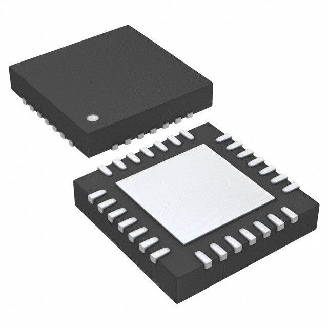
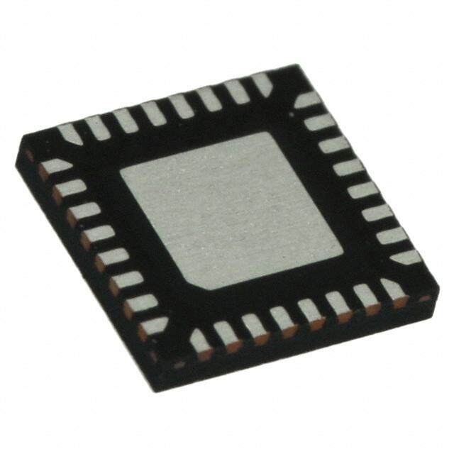
| 描述 | IC CODEC AUDIO FLEXSOUND 56TQFN |
| 产品分类 | |
| 品牌 | Maxim Integrated |
| 数据手册 | |
| 产品图片 |
|
| 产品型号 | MAX98089ETN+T |
| rohs | 无铅 / 符合限制有害物质指令(RoHS)规范要求 |
| 产品系列 | FlexSound™ |
| 三角积分 | 无 |
| 产品培训模块 | http://www.digikey.cn/PTM/IndividualPTM.page?site=cn&lang=zhs&ptm=25703http://www.digikey.cn/PTM/IndividualPTM.page?site=cn&lang=zhs&ptm=25705 |
| 供应商器件封装 | 56-TQFN-EP(7x7) |
| 信噪比,ADC/DAC(db)(典型值) | 93 / 101 |
| 其它名称 | MAX98089ETN+TDKR |
| 分辨率(位) | 24 b |
| 动态范围,ADC/DAC(db)(典型值) | 93 / 101 |
| 包装 | Digi-Reel® |
| 安装类型 | 表面贴装 |
| 封装/外壳 | 56-WFQFN 裸露焊盘 |
| 工作温度 | -40°C ~ 85°C |
| 应用说明 | |
| 数据接口 | I²C, 串行 |
| 标准包装 | 1 |
| 特色产品 | http://www.digikey.cn/product-highlights/cn/zh/maxim-tini-audio-codec-with-flexsound-processor/2955 |
| 电压-电源,数字 | 1.65 V ~ 3.6 V |
| 电压-电源,模拟 | 1.65 V ~ 2 V |
| 类型 | 立体声音频 |


- 商务部:美国ITC正式对集成电路等产品启动337调查
- 曝三星4nm工艺存在良率问题 高通将骁龙8 Gen1或转产台积电
- 太阳诱电将投资9.5亿元在常州建新厂生产MLCC 预计2023年完工
- 英特尔发布欧洲新工厂建设计划 深化IDM 2.0 战略
- 台积电先进制程称霸业界 有大客户加持明年业绩稳了
- 达到5530亿美元!SIA预计今年全球半导体销售额将创下新高
- 英特尔拟将自动驾驶子公司Mobileye上市 估值或超500亿美元
- 三星加码芯片和SET,合并消费电子和移动部门,撤换高东真等 CEO
- 三星电子宣布重大人事变动 还合并消费电子和移动部门
- 海关总署:前11个月进口集成电路产品价值2.52万亿元 增长14.8%


PDF Datasheet 数据手册内容提取
EVALUATION KIT AVAILABLE AVAILABLE MAX98089 Low-Power, Stereo Audio Codec with FlexSound Technology General Description Features The MAX98089 is a full-featured audio codec whose high S 5.6mW Power Comsumption (DAC to HP at 97dB DR) performance and low power consumption make it ideal S 101dB DR Stereo DAC (8kHz < fS < 96kHz) for portable applications. S 93dB DR Stereo ADC (8kHz < fS < 96kHz) Class D speaker amplifiers provide efficient amplification S Stereo Low EMI Class D Amplifiers for two speakers. Low radiated emissions enable com- 1.7W/Channel (8I, VSPK�VDD = 5.0V) pletely filterless operation. Integrated bypass switches 2.9W/Channel (4I, VSPK�VDD = 5.0V) optionally connect an external amplifier to the transducer S Efficient Class H Headphone Amplifier when the Class D amplifiers are disabled. S Differential Receiver Amplifier/Stereo Line Outputs The IC features a stereo Class H headphone amplifier S 2 Stereo Single-Ended/Mono Differential Line that utilizes a dual-mode charge pump to maximize effi- Inputs ciency while outputting a ground referenced signal that S 3 Differential Microphone Inputs does not require output coupling capacitors. S FlexSound Technology The IC also features a mono differential amplifier that can 5-Band Parametric EQ also be configured as a stereo line output. Automatic Level Control (ALC) Excursion Limiter Two differential analog microphone inputs are available as Speaker Power Limiter well as support for two PDM digital microphones. Integrated Speaker Distortion Limiter switches allow for an additional microphone input as well Microphone Automatic Gain Control as microphone signals to be routed out to external devices. and Noise Gate Two flexible single-ended or differential line inputs may be S Dual I2S/PCM/TDM Digital Audio Interfaces connected to an FM radio or other sources. S Asynchronous Digital Mixing Integrated FlexSoundK technology improves loudspeak- S Supports Master Clock Frequencies from 10MHz er performance by optimizing the signal level and fre- to 60MHz quency response while limiting the maximum distortion S RF Immune Analog Inputs and Outputs and power at the output to prevent speaker damage. S Extensive Click-and-Pop Reduction Circuitry Automatic gain control (AGC) and a noise gate optimize S Available in 63-Bump WLP Package (3.80mm x the signal level of micrFopuhnonce tinipount saigln Dalsi atog mraakem bsest 3.30mm, 0.4mm Pitch) and 56-Pin TQFN Package use of the ADC dynamic range. (7mm x 7mm x 0.75mm) The device is fully specified over the -40NC to +85NC Ordering Information appears at end of data sheet. extended temperature range. For related parts and recommended products to use with this part, FlexSound is a trademark of Maxim Integrated Products, Inc. refer to www.maxim-ic.com/MAX98089.related. Simplified Block Diagram I2C I2S/PCM I2S/PCM RECEIVER/LINEOUT AMPS DIGITAL DIGITAL CONTROL AUDIO AUDIO DIGITAL MICROPHONE INTERFACE INTERFACE INPUT FLEXSOUND TECHNOLOGY • 5-BAND PARAMETRIC EQ ADC •• ALOUUTODMSPAETAICK ELRE VPERLO CCOESNSTIRNOGL DAC SPEAKER AMP • EXCURSION LIMITER MIX •• TPHODW LEIRM LITIMERITER LINEIN A1 • MICROPHONE PROCESSING SPEAKER AMP ADC •• ANUOTISOEM GAATTICE GAIN CONTROL MIX • ASYNCHRONOUS DIGITAL MIXING DAC LINEIN A2 + HEADPHONE AMP Pin Configurations appear at end of data sheet. MAX98089 LINEIN B1 Functional Diagrams continued at end of data sheet. UCSP is a trademark of Maxim Integrated Products, Inc. LINEIN B2 + HEADPHONE AMP For pricing, delivery, and ordering information, please contact Maxim Direct at 1-888-629-4642, or visit Maxim’s website at www.maximintegrated.com. 19-5865; Rev 1; 3/12
MAX98089 Low-Power, Stereo Audio Codec with FlexSound Technology TABLE OF CONTENTS General Description ............................................................................ 1 Features ..................................................................................... 1 Simplified Block Diagram........................................................................ 1 Functional Diagram ............................................................................ 5 Absolute Maximum Ratings ...................................................................... 6 Electrical Characteristics ........................................................................ 6 Digital Input/Output Characteristics............................................................... 19 Input Clock Characteristics ..................................................................... 21 Audio Interface Timing Characteristics ............................................................ 22 Digital Microphone Timing Characterstics.......................................................... 23 I2C Timing Characteristics...................................................................... 24 Power Consumption........................................................................... 25 Typical Operating Characteristics ................................................................ 28 Microphone to ADC..........................................................................28 Line to ADC................................................................................32 Line-In Pin Direct to ADC .....................................................................33 Digital Loopback............................................................................33 Analog Loopback ...........................................................................34 DAC to Receiver ............................................................................35 Line to Receiver ............................................................................37 DAC-to-Line Output .........................................................................38 Line-to-Line Output..........................................................................38 DAC to Speaker.............................................................................39 Line to Speaker.............................................................................44 DAC to Headphone..........................................................................45 Line to Headphone ..........................................................................52 Speaker Bypass Switch ......................................................................54 Pin Configuration ............................................................................. 55 Pin Description............................................................................... 57 Detailed Description........................................................................... 60 I2C Slave Address...........................................................................61 Registers..................................................................................61 Power Management .........................................................................67 Microphone Inputs ..........................................................................69 Line Inputs.................................................................................71 Maxim Integrated 2
MAX98089 Low-Power, Stereo Audio Codec with FlexSound Technology TABLE OF CONTENTS (continued) ADC Input Mixers ...........................................................................72 Record Path Signal Processing.................................................................73 Microphone AGC.........................................................................73 Noise Gate..............................................................................73 ADC Record Level Control ....................................................................76 Sidetone ..................................................................................77 Digital Audio Interfaces.......................................................................78 Clock Control...............................................................................85 Sample Rate Converter.......................................................................88 Passband Filtering...........................................................................89 Playback Path Signal Processing ...............................................................92 Automatic Level Control....................................................................92 Parametric Equalizer ......................................................................93 Playback Level Control .......................................................................95 DAC Input Mixers ...........................................................................96 Receiver Amplifier...........................................................................97 Receiver Output Mixer.....................................................................98 Receiver Output Volume ...................................................................99 Speaker Amplifiers .........................................................................100 Speaker Output Mixers ...................................................................101 Speaker Amplifier Signal Processing ...........................................................102 Excursion Limiter ........................................................................102 Speaker Output Volume...................................................................102 Power Limiter ...........................................................................105 Distortion Limiter ........................................................................106 Headphone . . . . . . . . . . . . . . . . . . . . . . . . . . . . . . . . . . . . . . . . . . . . . . . . . . . . . . . . . . . . . . . . . . . . . . . . . . . . . . .107 DirectDrive Headphone Amplifier ...........................................................107 Charge Pump...........................................................................107 Class H Operation .......................................................................108 Headphone Ground Sense (HPSNS).........................................................108 Headphone Output Mixers.................................................................110 Headphone Output Volume................................................................ 111 Output Bypass Switches.....................................................................112 Click-and-Pop Reduction ....................................................................113 Maxim Integrated 3
MAX98089 Low-Power, Stereo Audio Codec with FlexSound Technology TABLE OF CONTENTS (continued) Jack Detection.............................................................................114 Jack Insertion...........................................................................114 Accessory Button Detection ...............................................................114 Jack Removal...........................................................................114 Battery Measurement .......................................................................116 Device Status .............................................................................117 Device Revision............................................................................118 I2C Serial Interface .........................................................................118 Bit Transfer.............................................................................118 START and STOP Conditions...............................................................118 Early STOP Conditions....................................................................118 Slave Address ..........................................................................119 Acknowledge...........................................................................119 Write Data Format .......................................................................119 Read Data Format .......................................................................120 Applications Information....................................................................... 121 Typical Operating Circuits....................................................................121 Filterless Class D Operation ..................................................................123 RF Susceptibility ...........................................................................123 Startup/Shutdown Sequencing................................................................123 Component Selection .......................................................................124 Optional Ferrite Bead Filter ................................................................124 Input Capacitor..........................................................................124 Charge-Pump Capacitor Selection ..........................................................124 Charge-Pump Flying Capacitor.............................................................125 Charge-Pump Holding Capacitors...........................................................125 Unused Pins ..............................................................................125 Recommended PCB Routing .................................................................126 Supply Bypassing, Layout, and Grounding ......................................................126 WLP Applications Information.................................................................127 Ordering Information ......................................................................... 127 Package Information.......................................................................... 128 Revision History ............................................................................. 131 Maxim Integrated 4
MAX98089 Low-Power, Stereo Audio Codec with FlexSound Technology Functional Diagram G6 F6 A6 B6 A3, B3 A4, B4 A5, B5 C4, C5 C3, D3 C1, C2 A1, B1 A2, B2 C9 C8 D9 A7 A9 REF REG RECP/LOUTL/RXINP RECN/LOUTR/RXINN SPKLVDD SPKLP SPKLN SPKLGND SPKRVDD SPKRP SPKRN SPKRGND HPL HPSNS HPR PVDD HPGND BIAS 98089 RECVOLL:+8dB TO -62dB 0dB RECLEN RECBYPRECVOLR:+8dB TO -62dB 0dBLINEMODERECRENSPKBYP SPVOLL:+8dB TO -62dB +6dB SPLEN POWER/DISTORTION LIMITER +6dB SPRENSPVOLR:+8dB TO -62dB MIXHPL_PATH SELHPVOLL:+3dB TO -67dB HPLEN MIXHPR_HPVOR:PATH SEL+3dB TO -67dB HPREN CHARGEPUMP HPVSSHPVDDC1NC1PB9B7B8A8 X A M MIX MIXRECL MIX MIXRECR MIX MIXSPL MIX MIXSPR MIX MIXHPL MIX MIXHPR G5AVDD G4DVDD DACLDALEN DACRDAREN D4D2E4E1F2F3G1G3G2LRCLKS1SDOUTS1SDINS1DVDDS1BCLKS2LRCLKS2SDOUTS2SDINS2DVDDS2 PORT S2PORT S1 SEL211112222KKTNKKTNUULLLLIIDDCCCCOOSSBRBRDDLLSS DAI2 HIZOFF1SDIEN1SDIEN2HIZOFF2MAS1MAS2MAS2 BITFRAMEDATADATABITFRAMEDATADATACLOCKCLOCKOUTPUTINPUTCLOCKCLOCKOUTPUTINPUT LBEN1 LBEN2MUX +LTEN1 DV1G:DVST:0/6/12/18dB0dB TO -60dBTMFLEXSOUND+SIDETONEMIXTECHNOLOGYDSTSMULTI BAND ALC DVEQ1:DVEQ2:0dB TO -15dB0dB TO -15dB AUTOMATIC5-BAND5-BANDGAINNOISE GATEPARAMETRICPARAMETRICCONTROLEQEQEQ1ENEQ2ENAUDIO/MODE1VOICEAVFLTEXCURSION LIMITERFILTERSMIXAVLG: 0/6/AVRG: 0/6/MIXDALAUDIO12/18dB12/18dBFILTERSAVL:0dBAVR:0dBDV2:TO -15dBTO -15dBDCB20dB TO -15dB SAMPLE RATESRMIX_CONVERTER AUDIO/VOICEFILTERSDV1:MIX0dB TO -15dBMODE1DVFLTMIXDAR AGNDN.C.DGND F1G7C6, C7, D5, D6, D7, E3 D1BCLKS1 SEL1 DAI1 MAS1 ADLENADCL ADCRADREN MIX MIXADL MIX MIXADR E2MCLK CLOCKCONTROL E5F5F4SCLSDAIRQ 2IC E6JACKSNSJACKDETECTION JDETEN F7MICBIASREG MBEN MIC1P/PGAM1:DIGMICDATAE8+20dB TO 0dB MIC1N/DIGMICCLKF8 PA1EN:EXTMIC0/20/30dBMIC2BYP PGAM2:G9MIC2P+20dB TO 0dB G8MIC2N PA2EN:EXTMIC0/20/30dBINABYP PGAINA:+20dB TO -6dBF9INA1/EXTMICPINADIFF PGAINA:+20dB TO -6dBE9+INA2/EXTMICN PGAINB:+20dB TO -6dBE7INB1INBDIFF PGAINB:+20dB TO -6dBD8INB2+ NOTE: BUMP NUMBERS SHOWN FOR WLP PACKAGE. SEE THE PIN DESCRIPTION SECTION FOR TQFN PINOUT. Maxim Integrated 5
MAX98089 Low-Power, Stereo Audio Codec with FlexSound Technology ABSOLUTE MAXIMUM RATINGS (Voltages with respect to AGND.) HPSNS ..............................(VHPGND - 0.3V) to (VHPGND + 0.3V) DVDD, AVDD, PVDD, HPVDD ..............................-0.3V to +2.2V HPL, HPR ..........................(VHPVSS - 0.3V) to (VHPVDD + 0.3V) SPKLVDD, SPKRVDD, DVDDS1, DVDDS2 ..........-0.3V to +6.0V RECP/LOUTL/RXINP, RECP/LOUTR/ DGND, HPGND, SPKLGND, SPKRGND ..............-0.1V to +0.1V RXINN ....................(VSPKLGND - 0.3V) to (VSPKLVDD + 0.3V) HPVSS ..............................(VHPGND - 2.2V) to (VHPGND + 0.3V) SPKLP, SPKLN ..........(VSPKLGND - 0.3V) to (VSPKLVDD + 0.3V) C1N ...................................(VHPVSS - 0.3V) to (VHPGND + 0.3V) SPKRP, SPKRN ........(VSPKRGND - 0.3V) to (VSPKRVDD + 0.3V) C1P ...................................(VHPGND - 0.3V) to (VHPVDD + 0.3V) Continuous Power Dissipation (TA = +70NC) REF, MICBIAS .................................-0.3V to (VSPKLVDD + 0.3V) 63-Bump WLP (derate 25.6mW/NC above +70NC) ........2.05W MCLK, SDINS1, SDINS2, JACKSNS, 56-Pin TQFN (derate 40mW/NC above +70NC) ...............3.2W SDA, SCL, IRQ .................................................-0.3V to +6.0V Operating Temperature Range ..........................-40NC to +85NC LRCLKS1, BCLKS1, SDOUTS1 .........-0.3V to (VDVDDS1 + 0.3V) Storage Temperature Range ............................-65NC to +150NC LRCLKS2, BCLKS2, SDOUTS2 .........-0.3V to (VDVDDS2 + 0.3V) Lead Temperature (TQFN only, soldering, 10s) .............+300NC REG, INA1/EXTMICP, INA2/EXTMICN, INB1, INB2, Soldering Temperature (reflow) ......................................+260NC MIC1P/DIGMICDATA, MIC1N/DIGMICCLK, MIC2P, MIC2N ..................................................-0.3V to +2.2V Stresses beyond those listed under “Absolute Maximum Ratings” may cause permanent damage to the device. These are stress ratings only, and functional opera- tion of the device at these or any other conditions beyond those indicated in the operational sections of the specifications is not implied. Exposure to absolute maximum rating conditions for extended periods may affect device reliability. ELECTRICAL CHARACTERISTICS (VAVDD = VPVDD = VDVDD = VDVDDS1 = VDVDDS2 = 1.8V, VSPKLVDD = VSPKRVDD = 3.7V. Speaker loads (ZSPK) connected between SPK_P and SPK_N. Receiver load (RREC) connected between RECP and RECN. Headphone loads (RHP) connected from HPL or HPR to HPGND. Line out loads (RLOUT) connected from LOUTL or LOUTR to SPKLGND. RLOAD = RHP = J, RREC = J, ZSPK = J, CREF = 2.2FF, CMICBIAS = CREG = 1FF, CC1N-C1P = 1FF, CHPVDD = CHPVSS = 1FF. AVMICPRE_ = +20dB, AVMICPGA_ = 0dB, AVDACATTN = 0dB, AVDACGAIN = 0dB, AVADCLVL = 0dB, AVADCGAIN = 0dB, AVPGAIN_ = 0dB, AVHP_ = 0dB, AVREC = 0dB, AVSPK_ = 0dB, MCLK = 12.288MHz, LRCLK = 48kHz, MAS = 0. TA = TMIN to TMAX, unless otherwise noted. Typical values are at TA = +25NC.) (Note 1) PARAMETER SYMBOL CONDITIONS MIN TYP MAX UNITS POWER SUPPLY VSPKLVDD, VSPKRVDD 2.8 5.5 Supply Voltage Range Guaranteed by PSRR VDVDD, VAVDD, VPVDD 1.65 1.8 2 V VDVDDS1, VDVDDS2 1.65 3.6 Analog 4.5 8 Full-duplex 8kHz mono, Speaker 1.6 2.3 receiver output, MAS = 1 Digital 1.3 2 DAC playback 48kHz Analog 1.9 3 Total Supply Current IVDD stereo, headphone Speaker 0.001 0.0058 mA (Notes 2 and 3) outputs, MAS = 1 Digital 2.47 3.5 DAC playback 48kHz Analog 3.6 6.5 stereo, speaker outputs, Speaker 6.41 8.5 MAS = 1 Digital 2.49 3.5 Analog 0.2 2 Shutdown Supply Current TA = +25NC Speaker 0.01 1 FA (Note 2) Digital 1 5 REF Voltage 2.5 V REG Voltage 0.79 V VSEN = 0 30 Shutdown to Full Operation ms VSEN = 1 17 Maxim Integrated 6
MAX98089 Low-Power, Stereo Audio Codec with FlexSound Technology ELECTRICAL CHARACTERISTICS (continued) (VAVDD = VPVDD = VDVDD = VDVDDS1 = VDVDDS2 = 1.8V, VSPKLVDD = VSPKRVDD = 3.7V. Speaker loads (ZSPK) connected between SPK_P and SPK_N. Receiver load (RREC) connected between RECP and RECN. Headphone loads (RHP) connected from HPL or HPR to HPGND. Line out loads (RLOUT) connected from LOUTL or LOUTR to SPKLGND. RLOAD = RHP = J, RREC = J, ZSPK = J, CREF = 2.2FF, CMICBIAS = CREG = 1FF, CC1N-C1P = 1FF, CHPVDD = CHPVSS = 1FF. AVMICPRE_ = +20dB, AVMICPGA_ = 0dB, AVDACATTN = 0dB, AVDACGAIN = 0dB, AVADCLVL = 0dB, AVADCGAIN = 0dB, AVPGAIN_ = 0dB, AVHP_ = 0dB, AVREC = 0dB, AVSPK_ = 0dB, MCLK = 12.288MHz, LRCLK = 48kHz, MAS = 0. TA = TMIN to TMAX, unless otherwise noted. Typical values are at TA = +25NC.) (Note 1) PARAMETER SYMBOL CONDITIONS MIN TYP MAX UNITS MICROPHONE TO ADC PATH fS = 8kHz, MODE = 0 (IIR voice), AVMICPRE_ = 0dB Dynamic Range DR 88 dB (Note 4) VIN = 0.1VP-P, fS = 8kHz, f = 1kHz -78 Total Harmonic Distortion + THD+N AVMICPRE_ = 0dB, VIN = 1VP-P, f = 1kHz -85 dB Noise AVMICPRE_ = +30dB, VIN = 32mVP-P, f = 1kHz -71 Common-Mode Rejection CMRR VIN = 100mVP-P, f = 217Hz 74 dB Ratio VAVDD = 1.65V to 1.95V, input referred, 50 62 MIC inputs unconnected Power-Supply Rejection Ratio PSRR f = 217Hz, VRIPPLE = 200mVP-P, input referred 62 dB f = 1kHz, VRIPPLE = 200mVP-P, input referred 62 f = 10kHz, VRIPPLE = 200mVP-P, input referred 55 MODE = 0 (IIR voice) 2.2 8kHz 1kHz, 0dB input, MODE = 0 (IIR voice) 1.1 highpass filter disabled 16kHz Path Phase Delay ms measured from analog MODE = 1 (FIR audio) 4.5 input to digital output 8kHz MODE = 1 (FIR audio) 0.76 48kHz MICROPHONE PREAMP Full-Scale Input AVMICPRE_ = 0dB 1.05 VP-P PA1EN/PA2EN = 01 0 Preamplifier Gain AVMICPRE_ (Note 5) PA1EN/PA2EN = 10 19.5 20 20.5 dB PA1EN/PA2EN = 11 29.5 30 30.5 PGAM1/PGAM2 = 0x00 19 20 21 PGA Gain AVMICPGA_ (Note 5) dB PGAM1/PGAM2 = 0x14 0 All gain settings, measured at MIC1P/ MIC Input Resistance RIN_MIC 50 kI MIC1N/MIC2P/MIC2N Maxim Integrated 7
MAX98089 Low-Power, Stereo Audio Codec with FlexSound Technology ELECTRICAL CHARACTERISTICS (continued) (VAVDD = VPVDD = VDVDD = VDVDDS1 = VDVDDS2 = 1.8V, VSPKLVDD = VSPKRVDD = 3.7V. Speaker loads (ZSPK) connected between SPK_P and SPK_N. Receiver load (RREC) connected between RECP and RECN. Headphone loads (RHP) connected from HPL or HPR to HPGND. Line out loads (RLOUT) connected from LOUTL or LOUTR to SPKLGND. RLOAD = RHP = J, RREC = J, ZSPK = J, CREF = 2.2FF, CMICBIAS = CREG = 1FF, CC1N-C1P = 1FF, CHPVDD = CHPVSS = 1FF. AVMICPRE_ = +20dB, AVMICPGA_ = 0dB, AVDACATTN = 0dB, AVDACGAIN = 0dB, AVADCLVL = 0dB, AVADCGAIN = 0dB, AVPGAIN_ = 0dB, AVHP_ = 0dB, AVREC = 0dB, AVSPK_ = 0dB, MCLK = 12.288MHz, LRCLK = 48kHz, MAS = 0. TA = TMIN to TMAX, unless otherwise noted. Typical values are at TA = +25NC.) (Note 1) PARAMETER SYMBOL CONDITIONS MIN TYP MAX UNITS MICROPHONE BIAS MICBIAS Output Voltage VMICBIAS ILOAD = 1mA 2.15 2.2 2.25 V Load Regulation ILOAD = 1mA to 2mA 0.5 4.5 mV Line Regulation VSPKLVDD = 2.8V to 5.5V 110 FV f = 217Hz, VRIPPLE (SPKLVDD) = 100mVP-P 92 Ripple Rejection dB f = 10kHz, VRIPPLE (SPKLVDD) = 100mVP-P 83 A-weighted, f = 20Hz to 20kHz 3.9 FVRMS Noise Voltage P-weighted, f = 20Hz to 4kHz 2.1 f = 1kHz 50 nV/√Hz MICROPHONE BYPASS SWITCH IMIC1_ = 100mA, INABYP = MIC2BYP = 1, On-Resistance RON 5 30 I VMIC2_ = VINA_ = 0V, AVDD, TA = +25NC Total Harmonic Distortion + VIN = 2VP-P, VCM = 0.9V, RL = 10kI, THD+N -80 dB Noise f = 1kHz, INABYP = MIC2BYP = 1 Off-Isolation VIN = 2VP-P, VCM = 0.9V, RL = 10kI, f = 1kHz 60 dB VMIC1_ = [0V, AVDD], VMIC2_/VINA_ = Off-Leakage Current -1 +1 FA [AVDD, 0V] LINE INPUT TO ADC PATH INA pin direct, fS = 48kHz, MODE = 1 Dynamic Range (Note 4) DR 93 dB (FIR audio) Total Harmonic Distortion + THD+N VIN = 1VP-P, f = 1kHz -82 -74 dB Noise Gain Error DC accuracy 1 % VAVDD = 1.65V to 1.95V, input referred, 57 68 line inputs unconnected, TA = +25NC f = 217Hz, VRIPPLE = 200mVP-P, 63 AVADC = 0dB, input referred Power-Supply Rejection Ratio PSRR dB f = 1kHz, VRIPPLE = 200mVP-P, 63 AVADC = 0dB, input referred f = 10kHz, VRIPPLE = 200mVP-P, 57 AVADC = 0dB, input referred Maxim Integrated 8
MAX98089 Low-Power, Stereo Audio Codec with FlexSound Technology ELECTRICAL CHARACTERISTICS (continued) (VAVDD = VPVDD = VDVDD = VDVDDS1 = VDVDDS2 = 1.8V, VSPKLVDD = VSPKRVDD = 3.7V. Speaker loads (ZSPK) connected between SPK_P and SPK_N. Receiver load (RREC) connected between RECP and RECN. Headphone loads (RHP) connected from HPL or HPR to HPGND. Line out loads (RLOUT) connected from LOUTL or LOUTR to SPKLGND. RLOAD = RHP = J, RREC = J, ZSPK = J, CREF = 2.2FF, CMICBIAS = CREG = 1FF, CC1N-C1P = 1FF, CHPVDD = CHPVSS = 1FF. AVMICPRE_ = +20dB, AVMICPGA_ = 0dB, AVDACATTN = 0dB, AVDACGAIN = 0dB, AVADCLVL = 0dB, AVADCGAIN = 0dB, AVPGAIN_ = 0dB, AVHP_ = 0dB, AVREC = 0dB, AVSPK_ = 0dB, MCLK = 12.288MHz, LRCLK = 48kHz, MAS = 0. TA = TMIN to TMAX, unless otherwise noted. Typical values are at TA = +25NC.) (Note 1) PARAMETER SYMBOL CONDITIONS MIN TYP MAX UNITS LINE INPUT PREAMP AVPGAIN_ = 0dB 1 Full-Scale Input VIN VP-P AVPGAIN_ = -6dB 1.4 PGAINA/PGAINB = 0x0 19 20 21 PGAINA/PGAINB = 0x1 13 14 15 PGAINA/PGAINB = 0x2 2 3 4 TA = +25NC Level Adjust Gain AVPGAIN_ PGAINA/PGAINB = 0x3 0 dB (Note 5) PGAINA/PGAINB = 0x4 -4 -3 -2 PGAINA/PGAINB = 0x5, -7 -6 -5 0x6, 0x7 AVPGAIN_ = +20dB 14.5 21 28 AVPGAIN_ = +14dB 20 AVPGAIN_ = +3dB 20 Input Resistance RIN kI AVPGAIN_ = 0dB 7.5 10 14 AVPGAIN_ = -3dB 20 AVPGAIN_ = -6dB 20 TA = +25NC 18 20 22 Feedback Resistance RIN_FB INAEXT/INBEXT = 1 kI TA = TMIN to TMAX 16 24 ADC LEVEL CONTROL ADC Level Adjust Range AVADCLVL AVL/AVR = 0xF to 0x0 (Note 5) -12 +3 dB ADC Level Step Size 1 dB ADC Gain Adjust Range AVADCGAIN AVLG/AVRG = 00 to 11 (Note 5) 0 18 dB ADC Gain Adjust Step Size 6 dB ADC DIGITAL FILTERS VOICE MODE IIR LOWPASS FILTER (MODE1 = 0) Ripple limit cutoff 0.441 x fs Passband Cutoff fPLP Hz -3dB cutoff 0.449 x fs Passband Ripple f < fPLP -0.1 +0.1 dB Stopband Cutoff fSLP 0.47 x fS Hz Stopband Attenuation f > fSLP 74 dB (Note 6) Maxim Integrated 9
MAX98089 Low-Power, Stereo Audio Codec with FlexSound Technology ELECTRICAL CHARACTERISTICS (continued) (VAVDD = VPVDD = VDVDD = VDVDDS1 = VDVDDS2 = 1.8V, VSPKLVDD = VSPKRVDD = 3.7V. Speaker loads (ZSPK) connected between SPK_P and SPK_N. Receiver load (RREC) connected between RECP and RECN. Headphone loads (RHP) connected from HPL or HPR to HPGND. Line out loads (RLOUT) connected from LOUTL or LOUTR to SPKLGND. RLOAD = RHP = J, RREC = J, ZSPK = J, CREF = 2.2FF, CMICBIAS = CREG = 1FF, CC1N-C1P = 1FF, CHPVDD = CHPVSS = 1FF. AVMICPRE_ = +20dB, AVMICPGA_ = 0dB, AVDACATTN = 0dB, AVDACGAIN = 0dB, AVADCLVL = 0dB, AVADCGAIN = 0dB, AVPGAIN_ = 0dB, AVHP_ = 0dB, AVREC = 0dB, AVSPK_ = 0dB, MCLK = 12.288MHz, LRCLK = 48kHz, MAS = 0. TA = TMIN to TMAX, unless otherwise noted. Typical values are at TA = +25NC.) (Note 1) PARAMETER SYMBOL CONDITIONS MIN TYP MAX UNITS VOICE MODE IIR HIGHPASS FILTER (MODE1 = 0) AVFLT = 0x1 (Elliptical tuned for fS = 16kHz + 0.0161 217Hz notch) x fS AVFLT = 0x2 (500Hz Butterworth tuned for fS = 0.0319 16kHz) x fS Passband Cutoff AVFLT = 0x3 (Elliptical tuned for fS = 8kHz + 217Hz 0.0321 fAHPPB Hz (-3dB from Peak) notch) x fS AVFLT = 0x4 (500Hz Butterworth tuned for fS = 0.0632 8kHz) x fS 0.0043 AVFLT = 0x5 (fS/240 Butterworth) x fS AVFLT = 0x1 (Elliptical tuned for fS = 16kHz + 0.0139 217Hz notch) x fS AVFLT = 0x2 (500Hz Butterworth tuned for fS = 0.0156 16kHz) x fS Stopband Cutoff AVFLT = 0x3 (Elliptical tuned for fS = 8kHz + 217Hz 0.0279 fAHPSB Hz (-30dB from Peak) notch) x fS AVFLT = 0x4 (500Hz Butterworth tuned for fS = 0.0312 8kHz) x fS 0.0018 AVFLT = 0x5 (fS/240 Butterworth) x fS DC Attenuation DCATTEN AVFLT ≠ 000 90 dB STEREO AUDIO MODE FIR LOWPASS FILTER (MODE1 = 1, DHF1 = 0, LRCLK < 50kHz) Ripple limit cutoff 0.43 x fS Passband Cutoff fPLP -3dB cutoff 0.48 x fS Hz -6.02dB cutoff 0.5 x fS Passband Ripple f < fPLP -0.1 +0.1 dB Stopband Cutoff fSLP 0.58 x fS Hz Stopband Attenuation f < fSLP 60 dB (Note 6) ADC STEREO AUDIO MODE FIR LOWPASS FILTER (MODE1 = 1, DHF1 = 1, LRCLK > 50kHz) Ripple limit cutoff 0.208 x fS Passband Cutoff fPLP Hz -3dB cutoff 0.28 x fS Passband Ripple f < fPLP -0.1 +0.1 dB Stopband Cutoff fSLP 0.417 x fS Hz Stopband Attenuation f < fSLP 60 dB Maxim Integrated 10
MAX98089 Low-Power, Stereo Audio Codec with FlexSound Technology ELECTRICAL CHARACTERISTICS (continued) (VAVDD = VPVDD = VDVDD = VDVDDS1 = VDVDDS2 = 1.8V, VSPKLVDD = VSPKRVDD = 3.7V. Speaker loads (ZSPK) connected between SPK_P and SPK_N. Receiver load (RREC) connected between RECP and RECN. Headphone loads (RHP) connected from HPL or HPR to HPGND. Line out loads (RLOUT) connected from LOUTL or LOUTR to SPKLGND. RLOAD = RHP = J, RREC = J, ZSPK = J, CREF = 2.2FF, CMICBIAS = CREG = 1FF, CC1N-C1P = 1FF, CHPVDD = CHPVSS = 1FF. AVMICPRE_ = +20dB, AVMICPGA_ = 0dB, AVDACATTN = 0dB, AVDACGAIN = 0dB, AVADCLVL = 0dB, AVADCGAIN = 0dB, AVPGAIN_ = 0dB, AVHP_ = 0dB, AVREC = 0dB, AVSPK_ = 0dB, MCLK = 12.288MHz, LRCLK = 48kHz, MAS = 0. TA = TMIN to TMAX, unless otherwise noted. Typical values are at TA = +25NC.) (Note 1) PARAMETER SYMBOL CONDITIONS MIN TYP MAX UNITS STEREO AUDIO MODE DC BLOCKING HIGHPASS FILTER (MODE1 = 1) Passband Cutoff 0.000125 fAHPPB AVFLT ≠ 000 Hz (-3dB from Peak) x fS DC Attenuation DCAtten AVFLT ≠ 000 90 dB MICROPHONE AUTOMATIC GAIN CONTROL AGCHLD = 01 50 AGC Hold Duration ms AGCHLD = 11 400 AGCATK = 00 2 AGC Attack Time ms AGCATK = 11 123 AGCRLS = 000 0.078 AGC Release Time s AGCRLS = 111 10 AGC Threshold Level AGCTH = 0x0 to 0xF -3 +18 dB AGC Threshold Step Size 1 dB AGC Gain (Note 5) 0 20 dB ADC NOISE GATE NG Threshold Level ANTH = 0x3 to 0xF, referred to 0dBFS -64 -16 dB NG Attenuation (Note 5) 0 12 dB ADC-TO-DAC DIGITAL SIDETONE (MODE = 0) DVST = 0x01 -0.5 Sidetone Gain Adjust Range AVSTGA dB DVST = 0x1F -60.5 Sidetone Gain Adjust Step 2 dB Size 1kHz, 0dB input, highpass filter 8kHz 2.2 Sidetone Path Phase Delay ms disabled 16kHz 1.1 ADC-TO-DAC DIGITAL LOOP-THROUGH PATH fS = 48kHz, MCLK = 12.288MHz, MODE = 1 Dynamic Range (Note 4) DR 83 93 dB (FIR audio), MIC to HP output, TA = +25NC Total Harmonic Distortion + f = 1kHz, fS = 48kHz, MCLK = 12.288MHz, MODE = THD+N 81 dB Noise 1 (FIR audio), MIC to HP output DAC LEVEL CONTROL DAC Attenuation Range AVDACATTN DV_ = 0xF to 0x0 (Note 5) -15 0 dB DAC Attenuation Step Size 1 dB DAC Gain Adjust Range AVDACGAIN DV1G = 00 to 11 (Note 5) 0 18 dB DAC Gain Adjust Step Size 6 dB Maxim Integrated 11
MAX98089 Low-Power, Stereo Audio Codec with FlexSound Technology ELECTRICAL CHARACTERISTICS (continued) (VAVDD = VPVDD = VDVDD = VDVDDS1 = VDVDDS2 = 1.8V, VSPKLVDD = VSPKRVDD = 3.7V. Speaker loads (ZSPK) connected between SPK_P and SPK_N. Receiver load (RREC) connected between RECP and RECN. Headphone loads (RHP) connected from HPL or HPR to HPGND. Line out loads (RLOUT) connected from LOUTL or LOUTR to SPKLGND. RLOAD = RHP = J, RREC = J, ZSPK = J, CREF = 2.2FF, CMICBIAS = CREG = 1FF, CC1N-C1P = 1FF, CHPVDD = CHPVSS = 1FF. AVMICPRE_ = +20dB, AVMICPGA_ = 0dB, AVDACATTN = 0dB, AVDACGAIN = 0dB, AVADCLVL = 0dB, AVADCGAIN = 0dB, AVPGAIN_ = 0dB, AVHP_ = 0dB, AVREC = 0dB, AVSPK_ = 0dB, MCLK = 12.288MHz, LRCLK = 48kHz, MAS = 0. TA = TMIN to TMAX, unless otherwise noted. Typical values are at TA = +25NC.) (Note 1) PARAMETER SYMBOL CONDITIONS MIN TYP MAX UNITS DAC DIGITAL FILTERS VOICE MODE IIR LOWPASS FILTER (MODE1 = 0) Ripple limit cutoff 0.448 x fS Passband Cutoff fPLP Hz -3dB cutoff 0.451 x fS Passband Ripple f < fPLP -0.1 +0.1 dB Stopband Cutoff fSLP 0.476 x fS Hz Stopband Attenuation f > fSLP 75 dB (Note 6) VOICE MODE IIR HIGHPASS FILTER (MODE1 = 0) DVFLT = 0x1 (Elliptical tuned for fS = 16kHz + 0.0161 217Hz notch) x fS DVFLT = 0x2 (500Hz Butterworth tuned for fS = 0.0312 16kHz) x fS Passband Cutoff DVFLT = 0x3 (Elliptical tuned for fS = 8kHz + 217Hz 0.0321 fDHPPB Hz (-3dB from Peak) notch) x fS DVFLT = 0x4 (500Hz Butterworth tuned for fS = 0.0625 8kHz) x fS 0.0042 DVFLT = 0x5 (fs/240 Butterworth) x fS DVFLT = 0x1 (Elliptical tuned for fS = 16kHz + 0.0139 x fS 217Hz notch) DVFLT = 0x2 (500Hz Butterworth tuned for fS = 0.0156 x fS 16kHz) Stopband Cutoff (-30dB from Peak) fDHPSB DVFLT = 0x3 (Elliptical tuned for fS = 8kHz + 217Hz 0.0279 x fS Hz notch) DVFLT = 0x4 (500Hz Butterworth tuned for fS = 0.0312 x fS 8kHz) DVFLT = 0x5 (fS/240 Butterworth) 0.0021 x fS DC Attenuation DCATTEN DVFLT ≠ 000 85 dB STEREO AUDIO MODE FIR LOWPASS FILTER (MODE1 = 1, DHF1/DHF2 = 0, LRCLK < 50kHz) Ripple limit cutoff 0.43 x fS Passband Cutoff fPLP -3dB cutoff 0.47 x fS Hz -6.02dB cutoff 0.5 x fS Passband Ripple f < fPLP -0.1 +0.1 dB Stopband Cutoff fSLP 0.58 x fS Hz Stopband Attenuation f > fSLP 60 dB (Note 6) Maxim Integrated 12
MAX98089 Low-Power, Stereo Audio Codec with FlexSound Technology ELECTRICAL CHARACTERISTICS (continued) (VAVDD = VPVDD = VDVDD = VDVDDS1 = VDVDDS2 = 1.8V, VSPKLVDD = VSPKRVDD = 3.7V. Speaker loads (ZSPK) connected between SPK_P and SPK_N. Receiver load (RREC) connected between RECP and RECN. Headphone loads (RHP) connected from HPL or HPR to HPGND. Line out loads (RLOUT) connected from LOUTL or LOUTR to SPKLGND. RLOAD = RHP = J, RREC = J, ZSPK = J, CREF = 2.2FF, CMICBIAS = CREG = 1FF, CC1N-C1P = 1FF, CHPVDD = CHPVSS = 1FF. AVMICPRE_ = +20dB, AVMICPGA_ = 0dB, AVDACATTN = 0dB, AVDACGAIN = 0dB, AVADCLVL = 0dB, AVADCGAIN = 0dB, AVPGAIN_ = 0dB, AVHP_ = 0dB, AVREC = 0dB, AVSPK_ = 0dB, MCLK = 12.288MHz, LRCLK = 48kHz, MAS = 0. TA = TMIN to TMAX, unless otherwise noted. Typical values are at TA = +25NC.) (Note 1) PARAMETER SYMBOL CONDITIONS MIN TYP MAX UNITS STEREO AUDIO MODE FIR LOWPASS FILTER (MODE1 = 1, DHF1/DHF2 = 1 for LRCLK > 50kHz) Ripple limit cutoff 0.24 x fS Passband Cutoff fPLP Hz -3dB cutoff 0.31 x fS Passband Ripple f < fPLP -0.1 +0.1 dB Stopband Cutoff fSLP 0.477 x fS Hz Stopband Attenuation f < fSLP 60 dB (Note 6) STEREO AUDIO MODE DC BLOCKING HIGHPASS FILTER Passband Cutoff 0.000104 fDHPPB DVFLT ≠ 000 (DAI1), DCB2 = 1 (DAI2) Hz (-3dB from Peak) x fS DC Attenuation DCATTEN DVFLT ≠ 000 (DAI1), DCB2 = 1 (DAI2) 90 dB AUTOMATIC LEVEL CONTROL Dual Band Lowpass Corner ALCMB = 1 5 kHz Frequency Dual Band Highpass Corner ALCMB = 1 5 kHz Frequency Gain Range 0 12 dB Low-Signal Threshold ALCTH = 111 to 001 -48 -12 dBFS ALCRLS = 101 0.25 Release Time s ALCRLS = 000 8 PARAMETRIC EQUALIZER Number of Bands 5 Bands Per Band Gain Range -12 +12 dB Preattenuator Gain Range (Note 5) -15 0 dB Preattenuator Step Size 1 dB DAC TO RECEIVER AMPLIFIER PATH Dynamic Range DR fS = 48kHz, f = 1kHz (Note 4) 96 dB Output Offset Voltage VOS AVREC_ = -62dB, TA = +25NC, WLP package only ±0.5 ±4 mV Total Harmonic Distortion + THD+N f = 1kHz, POUT = 15mW, RREC = 32I -70 -63 dB Noise VSPKLVDD = 2.8V to 5.5V, TA = +25NC 64 75 f = 217Hz, VRIPPLE = 200mVP-P 80 Power-Supply Rejection Ratio PSRR dB f = 1kHz, VRIPPLE = 200mVP-P 80 f = 10kHz, VRIPPLE = 200mVP-P 77 Maxim Integrated 13
MAX98089 Low-Power, Stereo Audio Codec with FlexSound Technology ELECTRICAL CHARACTERISTICS (continued) (VAVDD = VPVDD = VDVDD = VDVDDS1 = VDVDDS2 = 1.8V, VSPKLVDD = VSPKRVDD = 3.7V. Speaker loads (ZSPK) connected between SPK_P and SPK_N. Receiver load (RREC) connected between RECP and RECN. Headphone loads (RHP) connected from HPL or HPR to HPGND. Line out loads (RLOUT) connected from LOUTL or LOUTR to SPKLGND. RLOAD = RHP = J, RREC = J, ZSPK = J, CREF = 2.2FF, CMICBIAS = CREG = 1FF, CC1N-C1P = 1FF, CHPVDD = CHPVSS = 1FF. AVMICPRE_ = +20dB, AVMICPGA_ = 0dB, AVDACATTN = 0dB, AVDACGAIN = 0dB, AVADCLVL = 0dB, AVADCGAIN = 0dB, AVPGAIN_ = 0dB, AVHP_ = 0dB, AVREC = 0dB, AVSPK_ = 0dB, MCLK = 12.288MHz, LRCLK = 48kHz, MAS = 0. TA = TMIN to TMAX, unless otherwise noted. Typical values are at TA = +25NC.) (Note 1) PARAMETER SYMBOL CONDITIONS MIN TYP MAX UNITS Peak voltage, A-weighted, 32 Into shutdown -68 Click-and-Pop Level KCP samples per second, AVREC = dBV 0dB Out of shutdown -72 LINE INPUT TO RECEIVER AMPLIFIER PATH Dynamic Range (Note 4) DR Referenced to full-scale output level 94 dB Total Harmonic Distortion + THD+N -64 dB Noise Peak voltage, A-weighted, 32 Into shutdown -51 Click-and-Pop Level KCP samples per second, AVREC = dBV 0dB Out of shutdown -49 RECEIVER AMPLIFIER Output Power POUT RREC = 32I, f = 1kHz, THD = 1% 92 mW Full-Scale Output (Note 7) 1 VRMS RECVOL = 0x00 -62 Volume Control (Note 5) AVREC dB RECVOL = 0x1F 8 +8dB to +6dB 0.5 +6dB to +0dB 1 Volume Control Step Size 0dB to -14dB 2 dB -14dB to -38dB 3 -38dB to -62dB 4 Mute Attenuation f = 1kHz 88 dB RREC = 32I 500 Capacitive Drive Capability No sustained oscillations pF RREC = J 100 DAC TO LINE OUT AMPLIFIER PATH Dynamic Range (Note 4) DR fS = 48kHz, f = 1kHz 83 96 dB Total Harmonic Distortion + THD+N f = 1kHz, RL = 1kI -78 -72 dB Noise LINE INPUT TO LINE OUT AMPLIFIER PATH Dynamic Range (Note 4) DR Referenced to full-scale output level 92 dB Total Harmonic Distortion + THD+N f = 1kHz, RL = 10kI 76 dB Noise Full-Scale Output (Note 7) 2 VP-P Mute Attenuation f = 1kHz 85 dB Output Offset Voltage VOS AVREC_ = -62dB, TQFN package only Q0.5 Q4 mV Capacitive Drive Capability No sustained oscillations, RL = 1kI 500 pF Maxim Integrated 14
MAX98089 Low-Power, Stereo Audio Codec with FlexSound Technology ELECTRICAL CHARACTERISTICS (continued) (VAVDD = VPVDD = VDVDD = VDVDDS1 = VDVDDS2 = 1.8V, VSPKLVDD = VSPKRVDD = 3.7V. Speaker loads (ZSPK) connected between SPK_P and SPK_N. Receiver load (RREC) connected between RECP and RECN. Headphone loads (RHP) connected from HPL or HPR to HPGND. Line out loads (RLOUT) connected from LOUTL or LOUTR to SPKLGND. RLOAD = RHP = J, RREC = J, ZSPK = J, CREF = 2.2FF, CMICBIAS = CREG = 1FF, CC1N-C1P = 1FF, CHPVDD = CHPVSS = 1FF. AVMICPRE_ = +20dB, AVMICPGA_ = 0dB, AVDACATTN = 0dB, AVDACGAIN = 0dB, AVADCLVL = 0dB, AVADCGAIN = 0dB, AVPGAIN_ = 0dB, AVHP_ = 0dB, AVREC = 0dB, AVSPK_ = 0dB, MCLK = 12.288MHz, LRCLK = 48kHz, MAS = 0. TA = TMIN to TMAX, unless otherwise noted. Typical values are at TA = +25NC.) (Note 1) PARAMETER SYMBOL CONDITIONS MIN TYP MAX UNITS DAC TO SPEAKER AMPLIFIER PATH Total Harmonic Distortion + THD+N f = 1kHz, POUT = 200mW, ZSPK = 8I + 68FH -68 dB Noise SPKL to SPKR and SPKR to SPKL, Crosstalk -88 dB POUT = 640mW, f = 1kHz Output Noise 53 FVRMS Peak voltage, A-weighted, Into shutdown 65 Click-and-Pop Level KCP 32 samples per second, dBV AVSPK_ = 0dB Out of shutdown 66 MIC INPUT TO SPEAKER AMPLIFIER PATH Dynamic Range (Note 4) DR Referenced to full-scale output level, AVSPK_ = 0dB 82 dB Total Harmonic Distortion + THD+N f = 1kHz, POUT = 200mW, RL = 8I + 68FH 71 dB Noise Peak voltage, A-weighted, 32 Into shutdown 55 Click-and-Pop Level KCP samples per second, AVSPK_ = dBV 0dB Out of shutdown 52 SPEAKER AMPLIFIER f = 1kHz, VSPKLVDD = VSPKRVDD = 5.0V 2950 THD = 10%, VSPKLVDD = VSPKRVDD = 4.2V 2060 ZSPK = 4I + VSPKLVDD = VSPKRVDD = 3.7V 1570 33FH VSPKLVDD = VSPKRVDD = 3.0V 1000 f = 1kHz, VSPKLVDD = VSPKRVDD = 5.0V 2320 THD = 1%, VSPKLVDD = VSPKRVDD = 4.2V 1620 ZSPK = 4I + VSPKLVDD = VSPKRVDD = 3.7V 1240 33FH VSPKLVDD = VSPKRVDD = 3.0V 785 Output Power POUT mW f = 1kHz, VSPKLVDD = VSPKRVDD = 5.0V 1730 THD = 10%, VSPKLVDD = VSPKRVDD = 4.2V 1210 ZSPK = 8I + VSPKLVDD = VSPKRVDD = 3.7V 930 68FH VSPKLVDD = VSPKRVDD = 3.0V 600 f = 1kHz, VSPKLVDD = VSPKRVDD = 5.0V 1365 THD = 1%, VSPKLVDD = VSPKRVDD = 4.2V 955 ZSPK = 8I + VSPKLVDD = VSPKRVDD = 3.7V 735 68FH VSPKLVDD = VSPKRVDD = 3.0V 475 Full-Scale Output (Note 7) 2 VRMS SPVOLL/SPVOLR = 0x00 -62 Volume Control AVSPK_ (Note 5) dB SPVOLL/SPVOLR = 0x1F +8 Maxim Integrated 15
MAX98089 Low-Power, Stereo Audio Codec with FlexSound Technology ELECTRICAL CHARACTERISTICS (continued) (VAVDD = VPVDD = VDVDD = VDVDDS1 = VDVDDS2 = 1.8V, VSPKLVDD = VSPKRVDD = 3.7V. Speaker loads (ZSPK) connected between SPK_P and SPK_N. Receiver load (RREC) connected between RECP and RECN. Headphone loads (RHP) connected from HPL or HPR to HPGND. Line out loads (RLOUT) connected from LOUTL or LOUTR to SPKLGND. RLOAD = RHP = J, RREC = J, ZSPK = J, CREF = 2.2FF, CMICBIAS = CREG = 1FF, CC1N-C1P = 1FF, CHPVDD = CHPVSS = 1FF. AVMICPRE_ = +20dB, AVMICPGA_ = 0dB, AVDACATTN = 0dB, AVDACGAIN = 0dB, AVADCLVL = 0dB, AVADCGAIN = 0dB, AVPGAIN_ = 0dB, AVHP_ = 0dB, AVREC = 0dB, AVSPK_ = 0dB, MCLK = 12.288MHz, LRCLK = 48kHz, MAS = 0. TA = TMIN to TMAX, unless otherwise noted. Typical values are at TA = +25NC.) (Note 1) PARAMETER SYMBOL CONDITIONS MIN TYP MAX UNITS +8dB to +6dB 0.5 +6dB to +0dB 1 Volume Control Step Size 0dB to -14dB 2 dB -14dB to -38dB 3 -38dB to -64dB 4 Mute Attenuation f = 1kHz 86 dB Output Offset Voltage VOS AVSPK_ = -61dB, TA = +25NC Q0.5 Q3 mV EXCURSION LIMITER Upper Corner Frequency DHPUCF = 001 to 100 400 1000 Hz Range Lower Corner Frequency DHPLCF = 01 to 10 400 Hz DHPUCF = 000 (fixed mode) 100 DHPUCF = 001 200 Biquad Minimum Corner DHPUCF = 010 300 Hz Frequency DHPUCF = 011 400 DHPUCF = 100 500 ZSPK = 8I + 68FH, VSP- DHPTH = 000 0.34 Threshold Voltage KLVDD = VSPKRVDD = 5.5V, VP AVSPK_ = 8dB DHPTH = 111 0.95 ALCRLS = 101 0.25 Release Time s ALCRLS = 000 4 POWER LIMITER Attenuation -64 dB ZSPK = 8I + 68FH, VSP- PWRTH = 0x1 0.08 Threshold KLVDD = VSPKRVDD = 5.5V, W AVSPK_ = 8dB PWRTH = 0xF 1.23 PWRT1 = 0x1 0.5 Time Constant 1 tPWR1 s PWRT1 = 0xF 8.7 PWRT2 = 0x1 to 0xF 0.5 Time Constant 2 tPWR2 min PWRT2 = 0xF 8.7 Weighting Factor kPWR PWRK = 000 to 111 12.5 100 % DISTORTION LIMITER THDCLP = 0x1 < 1 Distortion Limit % THDCLP = 0xF 24 THDT1 = 000 0.76 Release Time Constant s THDT1 = 111 6.2 Maxim Integrated 16
MAX98089 Low-Power, Stereo Audio Codec with FlexSound Technology ELECTRICAL CHARACTERISTICS (continued) (VAVDD = VPVDD = VDVDD = VDVDDS1 = VDVDDS2 = 1.8V, VSPKLVDD = VSPKRVDD = 3.7V. Speaker loads (ZSPK) connected between SPK_P and SPK_N. Receiver load (RREC) connected between RECP and RECN. Headphone loads (RHP) connected from HPL or HPR to HPGND. Line out loads (RLOUT) connected from LOUTL or LOUTR to SPKLGND. RLOAD = RHP = J, RREC = J, ZSPK = J, CREF = 2.2FF, CMICBIAS = CREG = 1FF, CC1N-C1P = 1FF, CHPVDD = CHPVSS = 1FF. AVMICPRE_ = +20dB, AVMICPGA_ = 0dB, AVDACATTN = 0dB, AVDACGAIN = 0dB, AVADCLVL = 0dB, AVADCGAIN = 0dB, AVPGAIN_ = 0dB, AVHP_ = 0dB, AVREC = 0dB, AVSPK_ = 0dB, MCLK = 12.288MHz, LRCLK = 48kHz, MAS = 0. TA = TMIN to TMAX, unless otherwise noted. Typical values are at TA = +25NC.) (Note 1) PARAMETER SYMBOL CONDITIONS MIN TYP MAX UNITS DAC TO HEADPHONE AMPLIFIER PATH Master or slave mode 101 Slave mode 97 Dynamic Range (Note 4) DR fS = 48kHz dB Low power mode, 95 97 TA = +25NC Total Harmonic Distortion + RHP = 16I -84 -64 THD+N f = 1kHz, POUT = 20mW dB Noise RHP = 32I -85 HPL to HPR and HPR to HPL, POUT = 5mW, Crosstalk -92 dB f = 1kHz, RHP = 32I VAVDD = VPVDD = 1.65V to 2.0V 46 54 f = 217Hz, VRIPPLE = 200mVP-P, 72 AVHP_ = 0dB Power-Supply Rejection Ratio PSRR f = 1kHz, VRIPPLE = 200mVP-P, dB 63 AVHP_ = 0dB f = 10kHz, VRIPPLE = 200mVP-P, 43 AVHP_ = 0dB MODE = 0 (voice) 8kHz 2.2 1kHz, 0dB input, highpass MODE = 0 (voice) 1.1 filter disabled measured 16kHz DAC Path Phase Delay ms from digital input to analog MODE = 1 (music) 4.5 output 8kHz MODE = 1 (music) 0.76 48kHz Gain Error 1 5 % Channel Gain Mismatch 1 % Peak voltage, A-weighted, Into shutdown -62 Click-and-Pop Level KCP 32 samples per second, dBV AVHP_ = 0dB Out of shutdown -63 LINE INPUT TO HEADPHONE AMPLIFIER PATH Total Harmonic Distortion + THD+N VIN = 1VP-P, f =1kHz, RHP = 32I 81 dB Noise Dynamic Range (Note 4) 92.5 dB Peak voltage, A-weighted, Into shutdown -62 Click-and-Pop Level KCP 32 samples per second, dBV AVHP_ = 0dB Out of shutdown -63 Maxim Integrated 17
MAX98089 Low-Power, Stereo Audio Codec with FlexSound Technology ELECTRICAL CHARACTERISTICS (continued) (VAVDD = VPVDD = VDVDD = VDVDDS1 = VDVDDS2 = 1.8V, VSPKLVDD = VSPKRVDD = 3.7V. Speaker loads (ZSPK) connected between SPK_P and SPK_N. Receiver load (RREC) connected between RECP and RECN. Headphone loads (RHP) connected from HPL or HPR to HPGND. Line out loads (RLOUT) connected from LOUTL or LOUTR to SPKLGND. RLOAD = RHP = J, RREC = J, ZSPK = J, CREF = 2.2FF, CMICBIAS = CREG = 1FF, CC1N-C1P = 1FF, CHPVDD = CHPVSS = 1FF. AVMICPRE_ = +20dB, AVMICPGA_ = 0dB, AVDACATTN = 0dB, AVDACGAIN = 0dB, AVADCLVL = 0dB, AVADCGAIN = 0dB, AVPGAIN_ = 0dB, AVHP_ = 0dB, AVREC = 0dB, AVSPK_ = 0dB, MCLK = 12.288MHz, LRCLK = 48kHz, MAS = 0. TA = TMIN to TMAX, unless otherwise noted. Typical values are at TA = +25NC.) (Note 1) PARAMETER SYMBOL CONDITIONS MIN TYP MAX UNITS HEADPHONE AMPLIFIER RHP = 32I 30 Output Power POUT f = 1kHz, THD = 1% mW RHP = 16I 38 Positive Charge-Pump Output VOUT ≤ VPVDD x 0.2V, RHP = J PVDD/2 HPVDD V Voltage VOUT > VPVDD x 0.2V, RHP = J PVDD Negative Charge-Pump Out- VOUT ≤ VPVDD x 0.2V, RHP = J -PVDD/2 HPVSS V put Voltage VOUT > VPVDD x 0.2V, RHP = J -PVDD Output Voltage Threshold (Output Voltage at which QPVDD the Charge Pump Switches VTH RL = J V x 0.2 Modes; VOUT Rising; Transi- tion from Split to Invert Mode) Full-Scale Output (Note 7) 1 VRMS HPVOL_ = 0x00 -67 Volume Control AVHP_ (Note 5) dB HPVOL_ = 0x1F +3 +3dB to +1dB 0.5 +1dB to -5dB 1 Volume Control Step Size -5dB to -19dB 2 dB -19dB to -43dB 3 -43dB to -67dB 4 Mute Attenuation f = 1kHz 100 dB TA = +25NC Q0.1 Q1 Output Offset Voltage VOS AVHP_ = -67dB mV TA = TMIN to TMAX Q3 RHP = 32I 500 Capacitive Drive Capability No sustained oscillations pF RHP = J 100 SPEAKER BYPASS SWITCH ISPKL_ = 100mA, SPKBYP = 1, On-Resistance RON 2.8 I VRXIN_ = [0V, VSPKLVDD] Total Harmonic Distortion + VIN = 2VP-P, VCM = VSPKLVDD/2, RS = 10I 60 THD+N ZSPK = 8I + 68FH, f = 1kHz, dB Noise SPKBYP = 1 RS = 0I 60 VIN = 2VP-P, VCM = VSPKLVDD/2, Off-Isolation 96 dB ZSPK = 8I + 68FH, f = 1kHz VRXIN_ = [0V, VSPKLVDD], Off-Leakage Current -20 +20 FA VSPKL_ = [VSPKLVDD, 0V] Maxim Integrated 18
MAX98089 Low-Power, Stereo Audio Codec with FlexSound Technology ELECTRICAL CHARACTERISTICS (continued) (VAVDD = VPVDD = VDVDD = VDVDDS1 = VDVDDS2 = 1.8V, VSPKLVDD = VSPKRVDD = 3.7V. Speaker loads (ZSPK) connected between SPK_P and SPK_N. Receiver load (RREC) connected between RECP and RECN. Headphone loads (RHP) connected from HPL or HPR to HPGND. Line out loads (RLOUT) connected from LOUTL or LOUTR to SPKLGND. RLOAD = RHP = J, RREC = J, ZSPK = J, CREF = 2.2FF, CMICBIAS = CREG = 1FF, CC1N-C1P = 1FF, CHPVDD = CHPVSS = 1FF. AVMICPRE_ = +20dB, AVMICPGA_ = 0dB, AVDACATTN = 0dB, AVDACGAIN = 0dB, AVADCLVL = 0dB, AVADCGAIN = 0dB, AVPGAIN_ = 0dB, AVHP_ = 0dB, AVREC = 0dB, AVSPK_ = 0dB, MCLK = 12.288MHz, LRCLK = 48kHz, MAS = 0. TA = TMIN to TMAX, unless otherwise noted. Typical values are at TA = +25NC.) (Note 1) PARAMETER SYMBOL CONDITIONS MIN TYP MAX UNITS RECEIVER BYPASS SWITCH IRECP = 100mA, RECBYP = 1, VRECN = [0V, VSPKL- On-Resistance RON 2 I VDD] Total Harmonic Distortion + VIN = 2VP-P, VCM = VSPKLVDD/2, ZSPK = 8I + THD+N 60 % Noise 68FH, f = 1kHz, RECBYP = 1, RS = 0I VIN = 2VP-P, VCM = VSPKLVDD/2, ZSPK = 8I + Off-Isolation 84 dB 68FH, f = 1kHz VRECP = [0V, VSPKLVDD], VRECN = Off-Leakage Current -15 +15 FA [VSPKLVDD, 0V] JACK DETECTION 0.92 x 0.95 x 0.98 x MICBIAS enabled VMICBIASVMICBIAS VMICBIAS JACKSNS High Threshold VTH1 V 0.92 x 0.95 x 0.98 x MICBIAS disabled VSPKLVDDVSPKLVDDVSPKLVDD 0.06 x 0.10 x 0.17 x MICBIAS enabled VMICBIASVMICBIAS VMICBIAS JACKSNS Low Threshold VTH2 V 0.06 x 0.10 x 0.17 x MICBIAS disabled VSPKLVDDVSPKLVDDVSPKLVDD JACKSNS Sense Voltage MICBIAS disabled, JDWK = 1 3.65 3.7 JACKSNS Sense Resistance RSENSE MICBIAS disabled, JDWK = 0 1.6 2.4 2.9 kI JACKSNS Weak Pullup Current IWPU MICBIAS disabled, JDWK = 1 2 5 9.5 FA JDEB = 00 25 JACKSNS Deglitch Period tGLITCH ms JDEB = 11 200 BATTERY ADC Input Voltage Range 2.6 5.6 V LSB Size 0.1 V DIGITAL INPUT/OUTPUT CHARACTERISTICS (VAVDD = VPVDD = VDVDD = VDVDDS1 = VDVDDS2 = 1.8V, VSPKLVDD = VSPKRVDD = 3.7V, TA = +25NC, unless otherwise noted.) (Note 1) PARAMETER SYMBOL CONDITIONS MIN TYP MAX UNITS MCLK Input High Voltage VIH 1.2 V Input Low Voltage VIL 0.6 V Input Leakage Current IIH, IIL VDVDD = 2.0V, VIN = 0V, 5.5V; TA = +25°C -1 +1 FA Input Capacitance 10 pF Maxim Integrated 19
MAX98089 Low-Power, Stereo Audio Codec with FlexSound Technology DIGITAL INPUT/OUTPUT CHARACTERISTICS (continued) (VAVDD = VPVDD = VDVDD = VDVDDS1 = VDVDDS2 = 1.8V, VSPKLVDD = VSPKRVDD = 3.7V, TA = +25NC, unless otherwise noted.) (Note 1) PARAMETER SYMBOL CONDITIONS MIN TYP MAX UNITS SDINS1, BCLKS1, LRCLKS1—INPUT 0.7 x Input High Voltage VIH V DVDDS1 0.29 x Input Low Voltage VIL V DVDDS1 Input Hysteresis 200 mV Input Leakage Current IIH, IIL VDVDDS1 = 3.6V, VIN = 0V, 3.6V; TA = +25°C -1 +1 FA Input Capacitance 10 pF BCLKS1, LRCLKS1, SDOUTS1—OUTPUT Output Low Voltage VOL VDVDDS1 = 1.65V, IOL = 3mA 0.4 V DVDDS1 Output High Voltage VOH VDVDDS1 = 1.65V, IOH = 3mA V - 0.4 Input Leakage Current IIH, IIL VDVDD = 2.0V, VIN = 0V, 5.5V; TA = +25°C, -1 +1 FA high-impedance state SDINS2, BCLKS2, LRCLKS2—INPUT 0.7 x Input High Voltage VIH V DVDDS2 0.29 x Input Low Voltage VIL V DVDDS2 Input Hysteresis 200 mV Input Leakage Current IIH, IIL VDVDDS2 = 3.6V, VIN = 0V, 3.6V; TA = +25°C -1 +1 FA Input Capacitance 10 pF BCLKS2, LRCLKS2, SDOUTS2—OUTPUT Output Low Voltage VOL VDVDDS2 = 1.65V, IOL = 3mA 0.4 V DVDDS2 Output High Voltage VOH VDVDDS2 = 1.65V, IOH = 3mA V - 0.4 VDVDD = 2.0V, VIN = 0V, 5.5V; TA = +25NC, Input Leakage Current IIH, IIL -1 +1 FA high-impedance state SDA, SCL—INPUT 0.7 x Input High Voltage VIH V DVDD 0.3 x Input Low Voltage VIL V DVDD Input Hysteresis 210 mV Input Leakage Current IIH, IIL VDVDD = 2.0V, VIN = 0V, 5.5V; TA = +25NC -1 +1 FA Input Capacitance 10 pF SDA, IRQ—OUTPUT Output High Current IOH VOUT = 5.5V, TA = +25°C 1 mA 0.2 x Output Low Voltage VOL VDVDD = 1.65V, IOL = 3mA V DVDD Maxim Integrated 20
MAX98089 Low-Power, Stereo Audio Codec with FlexSound Technology DIGITAL INPUT/OUTPUT CHARACTERISTICS (continued) (VAVDD = VPVDD = VDVDD = VDVDDS1 = VDVDDS2 = 1.8V, VSPKLVDD = VSPKRVDD = 3.7V, TA = +25NC, unless otherwise noted.) (Note 1) PARAMETER SYMBOL CONDITIONS MIN TYP MAX UNITS DIGMICDATA—INPUT 0.65 x Input High Voltage VIH V DVDD 0.35 x Input Low Voltage VIL V DVDD Input Hysteresis 125 mV Input Leakage Current IIH, IIL VDVDD = 2.0V, VIN = 0V, 2.0V; TA = +25°C -25 +25 FA Input Capacitance 10 pF DIGMICCLK—OUTPUT Output Low Voltage VOL VDVDD = 1.65V, IOL = 1mA 0.4 V DVDD - Output High Voltage VOH VDVDD = 1.65V, IOH = 1mA V 0.4 INPUT CLOCK CHARACTERISTICS (VAVDD = VPVDD = VDVDD = VDVDDS1 = VDVDDS2 = 1.8V, VSPKLVDD = VSPKRVDD = 3.7V, TA = +25NC, unless otherwise noted.) (Note 1) PARAMETER SYMBOL CONDITIONS MIN TYP MAX UNITS MCLK Input Frequency fMCLK 10 60 MHz PSCLK = 01 40 50 60 MCLK Input Duty Cycle % PSCLK = 10 or 11 30 70 Maximum MCLK Input Jitter 100 psRMS DHF_ = 0 8 48 LRCLK Sample Rate (Note 8) kHz DHF_ = 1 48 96 DAI1 LRCLK Average Frequency FREQ1 = 0x8 to 0xF 0 0 % Error (Note 9) FREQ1 = 0x0 -0.025 +0.025 DAI2 LRCLK Average Frequency -0.025 +0.025 % Error (Note 9) Rapid lock mode 2 7 PLL Lock Time ms Nonrapid lock mode 12 25 Maximum LRCLK Jitter to Maintain 100 ns PLL Lock Soft-Start/Stop Time 10 ms Maxim Integrated 21
MAX98089 Low-Power, Stereo Audio Codec with FlexSound Technology AUDIO INTERFACE TIMING CHARACTERISTICS (VAVDD = VPVDD = VDVDD = VDVDDS1 = VDVDDS2 = 1.8V, VSPKLVDD = VSPKRVDD = 3.7V, TA = +25NC, unless otherwise noted.) (Note 1) PARAMETER SYMBOL CONDITIONS MIN TYP MAX UNITS BCLK Cycle Time tBCLK Slave mode 90 ns BCLK High Time tBCLKH Slave mode 20 ns BCLK Low Time tBCLKL Slave mode 20 ns BCLK or LRCLK Rise and Fall Time tR, tF Master mode, CL = 15pF 5 ns SDIN to BCLK Setup Time tSETUP 20 ns LRCLK to BCLK Setup Time tSYNCSET Slave mode 20 ns SDIN to BCLK Hold Time tHOLD 20 ns LRCLK to BCLK Hold Time tSYNCHOLD Slave mode 20 ns Minimum Delay Time from LSB BCLK Falling Edge to tHIZOUT Master mode, TDM_ = 1 42 ns High-Impedance State LRCLK Rising Edge to SDOUT tSYNCTX CL = 30pF, TDM_ = 1, FSW_ = 1 50 ns MSB Delay TDM_ = 1, BCLK rising edge 50 BCLK to SDOUT Delay tCLKTX CL = 30pF ns TDM_ = 0 50 TDM_ = 1 -15 +15 Master Delay Time from BCLK to LRCLK tCLKSYNC 0.8 x ns mode TDM_ = 0 tBCLKL Delay Time from LRCLK to BCLK Master tENDSYNC TDM_ = 1, FSW_ = 1 20 ns After LSB mode tBCLK tF BCLKtR BCLK tBCLKH tBCLKL (OUTPUT) (INPUT) tCLKSYNC tSYNCSET LRCLK LRCLK (OUTPUT) (INPUT) tHIZOUT tCLKTX tHIZOUT tCLKTX SDOUT SDOUT LSB HI-Z MSB LSB HI-Z MSB (OUTPUT) (OUTPUT) tSETUP tHOLD tSETUP tHOLD SDIN SDIN LSB MSB LSB MSB (INPUT) (INPUT) MASTER MODE SLAVE MODE Figure 1. Non-TDM Audio Interface Timing Diagrams (TDM_ = 0) Maxim Integrated 22
MAX98089 Low-Power, Stereo Audio Codec with FlexSound Technology tBCLK tF tR tBCLKH tBCLKL BCLK (OUTPUT) BCLK (INPUT) tCLKSYNC tCLKSYNC tSYNCSET tSYNCHOLD LRCLK (OUTPUT) LRCLK (INPUT) tHIZOUT tCLKTX tHIZOUT tCLKTX SDOUT (OUTPUT) LSB HI-Z MSB SDOUT (OUTPUT) LSB HI-Z MSB tSETUP tHOLD tSETUP tHOLD SDIN (INPUT) LSB MSB SDIN (INPUT) LSB MSB MASTER MODE SLAVE MODE Figure 2. TDM Audio Interface Timing Diagram (TDM_ = 1, FSW_ = 0) tBCLK tF tR tBCLKH tBCLKL BCLK (OUTPUT) BCLK (INPUT) tENDSYNC tCLKSYNC LRCLK (OUTPUT) LRCLK (INPUT) tHIZOUT tSYNCTX tCLKTX tHIZOUT tSYNCTX tCLKTX SDOUT (OUTPUT) LSB HI-Z MSB SDOUT (OUTPUT) LSB HI-Z MSB tSETUP tHOLD tSETUP tHOLD SDIN (INPUT) LSB MSB SDIN (INPUT) LSB MSB MASTER MODE SLAVE MODE Figure 3. TDM Audio Interface Timing Diagram (TDM_ = 1, FSW_ = 1) DIGITAL MICROPHONE TIMING CHARACTERSTICS (VAVDD = VHPVDD = VDVDD = VDVDDS1 = VDVDDS2 = 1.8V, VSPKLVDD = VSPKRVDD = 3.7V, TA = +25NC, unless otherwise noted.) (Note 1) PARAMETER SYMBOL CONDITIONS MIN TYP MAX UNITS MICCLK = 00 PCLK/8 MICCLK = 01 PCLK/6 DIGMICCLK Frequency fMICCLK MHz 64 x MICCLK = 10 fLRCLK DIGMICDATA to DIGMICCLK tSU,MIC Either clock edge 20 ns Setup Time DIGMICDATA to DIGMICCLK tHD,MIC Either clock edge 0 ns Hold Time Maxim Integrated 23
MAX98089 Low-Power, Stereo Audio Codec with FlexSound Technology 1/fMICCLK tHD,MIC tSU,MIC tHD,MIC tSU,MIC LEFT RIGHT LEFT RIGHT Figure 4. Digital Microphone Timing Diagram I2C TIMING CHARACTERISTICS (VAVDD = VPVDD = VDVDD = VDVDDS1 = VDVDDS2 = 1.8V, VSPKLVDD = VSPKRVDD = 3.7V, TA = +25NC, unless otherwise noted.) (Note 1) PARAMETER SYMBOL CONDITIONS MIN TYP MAX UNITS Guaranteed by SCL pulse-width low and Serial-Clock Frequency fSCL 0 400 kHz high Bus Free Time Between STOP and tBUF 1.3 Fs START Conditions Hold Time (Repeated) START tHD,STA 0.6 Fs Condition SCL Pulse-Width Low tLOW 1.3 Fs SCL Pulse-Width High tHIGH 0.6 Fs Setup Time for a Repeated START tSU,STA 0.6 Fs Condition Data Hold Time tHD,DAT RPU = 475I, CB = 100pF, 400pF 0 900 ns Data Setup Time tSU,DAT 100 ns 20 + SDA and SCL Receiving Rise Time tR (Note 10) 300 ns 0.1CB 20 + SDA and SCL Receiving Fall Time tF (Note 10) 300 ns 0.1CB 20 + SDA Transmitting Fall Time tF RPU = 475I, CB = 100pF, 400pF (Note 10) 250 ns 0.05CB Setup Time for STOP Condition tSU,STO 0.6 Fs Bus Capacitance CB Guaranteed by SDA transmitting fall time 400 pF Pulse Width of Suppressed Spike tSP 0 50 ns Maxim Integrated 24
MAX98089 Low-Power, Stereo Audio Codec with FlexSound Technology I2C TIMING CHARACTERISTICS (continued) (VAVDD = VPVDD = VDVDD = VDVDDS1 = VDVDDS2 = 1.8V, VSPKLVDD = VSPKRVDD = 3.7V, TA = +25NC, unless otherwise noted.) (Note 1) SDA tSU,STA tBUF tLOW tSU,DAT tHD,DAT tHD,STA tSP tSU,STO SCL tHIGH tHD,STA tR tF START CONDITION REPEATED START CONDITION STOP START CONDITION CONDITION Figure 5. I2C Interface Timing Diagram Note 1: The IC is 100% production tested at TA = +25NC. Specifications over temperature limits are guaranteed by design. Note 2: Analog supply current = IAVDD + IHPVDD. Speaker supply current = ISPKLVDD + ISPKRVDD. Digital supply current = IDVDD + IDVDDS1 + IDVDDS2. Note 3: Clocking all zeros into the DAC. Note 4: Dynamic range measured using the EIAJ method. -60dBFS, 1kHz output signal, A-weighted and normalized to 0dBFS. f = 20Hz to 20kHz. Note 5: Gain measured relative to the 0dB setting. Note 6: The filter specification is accurate only for synchronous clocking modes, where NI is a multiple of 0x1000. Note 7: 0dBFS for DAC input. 1VP-P for INA/INB inputs. Note 8: LRCLK may be any rate in the indicated range. Asynchronous or noninteger MCLK/LRCLK ratios may exhibit some full- scale performance degradation compared to synchronous integer related MCLK/LRCLK ratios. Note 9: In master-mode operation, the accuracy of the MCLK input proportionally determines the accuracy of the sample clock rate. Note 10: CB is in pF. Power Consumption (VAVDD = VPVDD = VDVDD = VDVDDS1 = VDVDDS2 = 1.8V, VSPKLVDD = VSPKRVDD = 3.7V, MAS = 0.) ISPKVDD + IDVDDS1 + IAVDD IPVDD IDVDD POWER DYNAMIC MODE ISPKLVDD IDVDDS2 (mA) (mA) (mA) (mW) RANGE (dB) (mA) (mA) Playback to Headphone Only DAC Playback 48kHz Stereo HP DAC ª HP 1.25 0.47 0.00 1.35 0.01 5.55 97 Low power mode, 24-bit, music filters, 256Fs DAC Playback 48kHz Stereo HP DAC ª HP Low power mode, 24-bit, music 1.25 1.81 0.00 1.56 0.01 8.32 97 filters, 256Fs, 0.1mW/channel, RHP = 32I Maxim Integrated 25
MAX98089 Low-Power, Stereo Audio Codec with FlexSound Technology Power Consumption (continued) (VAVDD = VPVDD = VDVDD = VDVDDS1 = VDVDDS2 = 1.8V, VSPKLVDD = VSPKRVDD = 3.7V, MAS = 0.) ISPKVDD + IDVDDS1 + IAVDD IPVDD IDVDD POWER DYNAMIC MODE ISPKLVDD IDVDDS2 (mA) (mA) (mA) (mW) RANGE (dB) (mA) (mA) DAC Playback to Headphone DAC Playback 48kHz Stereo HP DAC ª HP 2.04 1.27 0.00 1.53 0.01 8.72 101 24-bit, music filters, 256Fs DAC Playback 48kHz Stereo HP DAC ª HP 2.04 2.11 0.00 1.74 0.01 10.63 101 24-bit, music filters, 256Fs, 0.1mW/ channel, RHP = 32I DAC Playback 44.1kHz Stereo HP DAC ª HP 2.03 1.27 0.00 1.41 0.01 8.46 101 24-bit, music filters DAC Playback 44.1kHz Stereo HP DAC ª HP 1.25 0.47 0.00 1.25 0.01 5.34 98 Low power mode, 24-bit, music filters DAC Playback 8kHz Stereo HP DAC ª HP 2.04 1.27 0.00 1.07 0.00 7.89 96 16-bit, voice filters DAC Playback 8kHz Stereo HP DAC ª HP 1.26 0.47 0.00 0.90 0.00 4.72 96 16-bit, low power mode, voice filters DAC Playback 8kHz Mono HP DAC ª HP 0.77 0.29 0.00 0.79 0.00 3.33 98 16-bit, low power mode, voice filters Line Playback Stereo HP INA ª HP 2.40 1.27 0.00 0.02 0.00 6.67 95 Single-ended inputs DAC Playback to Class D Speaker DAC Playback 48kHz Stereo SPK DAC ª SPK 2.31 0.00 6.33 2.14 0.01 31.44 92 24-bit, music filters Maxim Integrated 26
MAX98089 Low-Power, Stereo Audio Codec with FlexSound Technology Power Consumption (continued) (VAVDD = VPVDD = VDVDD = VDVDDS1 = VDVDDS2 = 1.8V, VSPKLVDD = VSPKRVDD = 3.7V, MAS = 0.) ISPKVDD + IDVDDS1 + IAVDD IPVDD IDVDD POWER DYNAMIC MODE ISPKLVDD IDVDDS2 (mA) (mA) (mA) (mW) RANGE (dB) (mA) (mA) DAC Playback 48kHz Mono SPK DAC ª SPK 1.35 0.00 3.23 1.84 0.01 17.69 92 24-bit, music filters Line Playback Mono SPK INA ª SPKL 1.01 0.00 3.24 0.03 0.00 13.83 93 Differential inputs Full Duplex Full-Duplex 8kHz Mono RCV MIC1 ª ADC Record = 93 6.32 0.00 1.54 1.24 0.01 19.33 DAC ª REC Playback = 94 16-bit, voice filters Full-Duplex 8kHz Stereo HP MIC1/2 ª ADC Record = 93 11.19 1.27 0.48 1.28 0.01 26.43 DAC ª HP Playback = 96 16-bit, mixer, voice filters Full-Duplex 8kHz Stereo HP MIC1/2 ª ADC Record = 93 7.12 0.47 0.48 1.10 0.02 17.44 DAC ª HP Playback = 96 16-bit, low power mode, voice filters Line Record Line Stereo Record 48kHz INA ª ADC 6.19 0.00 0.20 1.31 0.15 14.47 91 24-bit, low power, music filters Line Stereo Record 48kHz INA ª ADC 5.69 0.00 0.20 1.31 0.12 13.53 93 Direct pin input, 24bit, low power, music filters Maxim Integrated 27
MAX98089 Low-Power, Stereo Audio Codec with FlexSound Technology Typical Operating Characteristics (VAVDD = VPVDD = VDVDD = VDVDDS1 = VDVDDS2 = 1.8V, VSPKLVDD = VSPKRVDD = 3.7V. Speaker loads (ZSPK) connected between SPK_P and SPK_N. Receiver load (RREC) connected between RECP and RECN. Headphone loads (RHP) connected from HPL or HPR to HPGND. Line out (RLOUT) connected from LOUTL or LOUTR to SPKLGND, CREF = 2.2FF, CMICBIAS = CREG = 1FF, CC1N-C1P = 1FF, CHPVDD = CHPVSS = 1FF. AVMICPRE_ = +20dB, AVMICPGA_ = 0dB, AVDACATTN = 0dB, AVDACGAIN = 0dB, AVADCLVL = 0dB, AVADCGAIN = 0dB, AVPGAIN_ = 0dB, AVHP_ = 0dB, AVREC = 0dB, AVSPK_ = 0dB, MCLK = 12.288MHz, LRCLK = 48kHz, MAS = 1. TA = +25NC, unless otherwise noted.) Microphone to ADC TOTAL HARMONIC DISTORTION PLUS TOTAL HARMONIC DISTORTION PLUS TOTAL HARMONIC DISTORTION PLUS NOISE vs. FREQUENCY (MIC TO ADC) NOISE vs. FREQUENCY (MIC TO ADC) NOISE vs. FREQUENCY (MIC TO ADC) 0 0 0 --2100 MLFRRCCELQLKK M = = O1 8D3kMEHHzz MAX98089 toc01 --2100 MLPRLCCLL LMKK O= = D1 4E34M.1HkHzz MAX98089 toc02 --2100 MLNRIC CMLLKOK D= =E 1 428.2kH88zMHz MAX98089 toc03 dB) -30 VAIVNM =IC 1PVRPE-_P = 0dB dB) -30 VAIVNM =IC 1PVRPE-_P = 0dB dB) -30 VAIVNM =IC 1PVRPE-_P = 0dB TIO ( -40 TIO ( -40 TIO ( -40 RA -50 RA RA -50 N N -50 N D+ -60 D+ D+ -60 H H H T T -60 T -70 -70 -80 -70 -80 -90 -80 -90 -100 -90 -100 10 100 1k 10k 10 100 1k 10k 100k 10 100 1k 10k 100k FREQUENCY (Hz) FREQUENCY (Hz) FREQUENCY (Hz) TOTAL HARMONIC DISTORTION PLUS TOTAL HARMONIC DISTORTION PLUS TOTAL HARMONIC DISTORTION PLUS NOISE vs. FREQUENCY (MIC TO ADC) NOISE vs. FREQUENCY (MIC TO ADC) NOISE vs. FREQUENCY (MIC TO ADC) 0 0 0 --2100 MLNRIC CMLLKOK D= =E 1 926.2kH88zMHz MAX98089 toc04 --2100 MLFRRCCELQLKK M = = O1 8D3kMEHHzz MAX98089 toc05 --2100 MLFRRCCELQLKK M = = O1 8D3kMEHHzz MAX98089 toc06 dB) -30 VAIVNM =IC 1PVRPE-_P = 0dB dB) -30 VAIVNM =IC 0P.R1EV_P -=P +20dB dB) -30 VAIVNM =IC 0P.R0E3_2 V=P +-P30dB O ( -40 O ( -40 O ( -40 TI TI TI RA -50 RA -50 RA -50 N N N D+ -60 D+ -60 D+ -60 H H H T T T -70 -70 -70 -80 -80 -80 -90 -90 -90 -100 -100 -100 10 100 1k 10k 100k 10 100 1k 10k 10 100 1k 10k FREQUENCY (Hz) FREQUENCY (Hz) FREQUENCY (Hz) Maxim Integrated 28
MAX98089 Low-Power, Stereo Audio Codec with FlexSound Technology Typical Operating Characteristics (continued) (VAVDD = VPVDD = VDVDD = VDVDDS1 = VDVDDS2 = 1.8V, VSPKLVDD = VSPKRVDD = 3.7V. Speaker loads (ZSPK) connected between SPK_P and SPK_N. Receiver load (RREC) connected between RECP and RECN. Headphone loads (RHP) connected from HPL or HPR to HPGND. Line out (RLOUT) connected from LOUTL or LOUTR to SPKLGND, CREF = 2.2FF, CMICBIAS = CREG = 1FF, CC1N-C1P = 1FF, CHPVDD = CHPVSS = 1FF. AVMICPRE_ = +20dB, AVMICPGA_ = 0dB, AVDACATTN = 0dB, AVDACGAIN = 0dB, AVADCLVL = 0dB, AVADCGAIN = 0dB, AVPGAIN_ = 0dB, AVHP_ = 0dB, AVREC = 0dB, AVSPK_ = 0dB, MCLK = 12.288MHz, LRCLK = 48kHz, MAS = 1. TA = +25NC, unless otherwise noted.) COMMON-MODE REJECTION POWER-SUPPLY REJECTION RATIO GAIN vs. FREQUENCY (MIC TO ADC) RATIO vs. FREQUENCY (MIC TO ADC) vs. FREQUENCY (MIC TO ADC) 10 90 120 -100 MODE = 1 MAX98089 toc07 7800 AVPRE = 20dB MAX98089 toc08 100 RIPPLE ON SPKLVDD, SPKRVDD MAX98089 toc09 NORMALIZED GAIN (dB) -----6543200000 MLRCCLLKK = = 1 83kMHHzz MODE = 0 CMRR (dB) 34560000 MLRCCLLKK = = 1 83kMAHAVHzVPzPRREE == 300ddBB PSRR (dB) 468000 MLNRIC CMLLKOK D= =E R1 4I2P8.P2kH8L8EzM OHNz AVDD, DVDD, HPVDD --8700 FVARIVNEM Q=IC 1MPVROPE-D_P E= 0dB 1200 FVCRIINNE Q== 11MVµOPF-DPE 20 VACVRINIMP =PIC L1PEµR =FE 2=0 00dmBVP-P -90 0 0 10 100 1k 10k 10 100 1k 10k 10 100 1k 10k 100k FREQUENCY (Hz) FREQUENCY (Hz) FREQUENCY (Hz) FFT, 0dBFS (MIC TO ADC) FFT, -60dBFS (MIC TO ADC) FFT, 0dBFS (MIC TO ADC) 20 0 20 -200 MLCRFLCRKLE =KQ 1=M3 8MOkDHHEzz MAX98089 toc10 --4200 MLCRFLCRKLE =KQ 1=M3 8MOkDHHEzz MAX98089 toc11 0 LRMCCLLKPK =L = L4 14M3.1MOkDHHEzz MAX98089 toc12 dBFS) --6400 AVMICPRE = 0dB dBFS) -60 AVMICPRE_ = 0dB dBFS) --4200 AVMICPRCEI_N == 01dµBF E ( E ( -80 E ( UD -80 UD UD -60 MPLIT-100 MPLIT-100 MPLIT -80 A-120 A-120 A -100 -140 -140 -160 -160 -120 -180 -180 -140 0 1 2 3 4 0 500 1k 1.5k 2k 2.5k 3k 3.5k 4k 0 5 10 15 20 FREQUENCY (kHz) FREQUENCY (Hz) FREQUENCY (kHz) Maxim Integrated 29
MAX98089 Low-Power, Stereo Audio Codec with FlexSound Technology Typical Operating Characteristics (continued) (VAVDD = VPVDD = VDVDD = VDVDDS1 = VDVDDS2 = 1.8V, VSPKLVDD = VSPKRVDD = 3.7V. Speaker loads (ZSPK) connected between SPK_P and SPK_N. Receiver load (RREC) connected between RECP and RECN. Headphone loads (RHP) connected from HPL or HPR to HPGND. Line out (RLOUT) connected from LOUTL or LOUTR to SPKLGND, CREF = 2.2FF, CMICBIAS = CREG = 1FF, CC1N-C1P = 1FF, CHPVDD = CHPVSS = 1FF. AVMICPRE_ = +20dB, AVMICPGA_ = 0dB, AVDACATTN = 0dB, AVDACGAIN = 0dB, AVADCLVL = 0dB, AVADCGAIN = 0dB, AVPGAIN_ = 0dB, AVHP_ = 0dB, AVREC = 0dB, AVSPK_ = 0dB, MCLK = 12.288MHz, LRCLK = 48kHz, MAS = 1. TA = +25NC, unless otherwise noted.) FFT, -60dBFS (MIC TO ADC) FFT, 0dBFS (MIC TO ADC) 0 20 -20 LRMCCLLKPK =L = L4 14M3.1MOkDHHEzz MAX98089 toc13 0 MCLLKR =C 1L2KN. 2=I 8 M488MOkDHHEzz MAX98089 toc14 -20 BFS) -40 AVMICPRE = 0dB BFS) -40 AVMICPCRINE == 01dµBF E (d -60 E (d UD UD -60 T T LI -80 LI MP MP -80 A A -100 -100 -120 -120 -140 -140 0 5 10 15 20 0 2 4 6 8 10 12 14 16 18 20 FREQUENCY (kHz) FREQUENCY (kHz) FFT, -60dBFS (MIC TO ADC) FFT, 0dBFS (MIC TO ADC) 0 20 -20 MCLLKR =C 1L2KN. 2=I 8 M488MOkDHHEzz MAX98089 toc15 0 MCLLKR =C 1L2KN. 2=I 8 M986MOkDHHEzz MAX98089 toc16 -20 BFS) -40 AVMICPRE_ = 0dB BFS) -40 AVMICPCRINE == 01dµBF E (d -60 E (d UD UD -60 T T LI -80 LI MP MP -80 A A -100 -100 -120 -120 -140 -140 0 5 10 15 20 0 2 4 6 8 10 12 14 16 18 20 FREQUENCY (kHz) FREQUENCY (kHz) Maxim Integrated 30
MAX98089 Low-Power, Stereo Audio Codec with FlexSound Technology Typical Operating Characteristics (continued) (VAVDD = VPVDD = VDVDD = VDVDDS1 = VDVDDS2 = 1.8V, VSPKLVDD = VSPKRVDD = 3.7V. Speaker loads (ZSPK) connected between SPK_P and SPK_N. Receiver load (RREC) connected between RECP and RECN. Headphone loads (RHP) connected from HPL or HPR to HPGND. Line out (RLOUT) connected from LOUTL or LOUTR to SPKLGND, CREF = 2.2FF, CMICBIAS = CREG = 1FF, CC1N-C1P = 1FF, CHPVDD = CHPVSS = 1FF. AVMICPRE_ = +20dB, AVMICPGA_ = 0dB, AVDACATTN = 0dB, AVDACGAIN = 0dB, AVADCLVL = 0dB, AVADCGAIN = 0dB, AVPGAIN_ = 0dB, AVHP_ = 0dB, AVREC = 0dB, AVSPK_ = 0dB, MCLK = 12.288MHz, LRCLK = 48kHz, MAS = 1. TA = +25NC, unless otherwise noted.) ADC ENABLE/DISABLE RESPONSE FFT, -60dBFS (MIC TO ADC) (MIC TO ADC) 0 MAX98089 toc18 -20 MCLLKR =C 1L2KN. 2=I 8 M986MOkDHHEzz MAX98089 toc17 S2VC/Ldiv S) -40 AVMICPRE_ = 0dB F B E (d -60 D U T LI -80 P M A ADC -100 OUTPUT 0.5V/div -120 -140 0 5 10 15 20 10ms/div FREQUENCY (kHz) SOFTWARE TURN-ON/OFF RESPONSE (MIC TO ADC) MAX98089 toc19 SCL 1V/div ADC OUTPUT 0.5V/div 10ms/div Maxim Integrated 31
MAX98089 Low-Power, Stereo Audio Codec with FlexSound Technology Typical Operating Characteristics (continued) (VAVDD = VPVDD = VDVDD = VDVDDS1 = VDVDDS2 = 1.8V, VSPKLVDD = VSPKRVDD = 3.7V. Speaker loads (ZSPK) connected between SPK_P and SPK_N. Receiver load (RREC) connected between RECP and RECN. Headphone loads (RHP) connected from HPL or HPR to HPGND. Line out (RLOUT) connected from LOUTL or LOUTR to SPKLGND, CREF = 2.2FF, CMICBIAS = CREG = 1FF, CC1N-C1P = 1FF, CHPVDD = CHPVSS = 1FF. AVMICPRE_ = +20dB, AVMICPGA_ = 0dB, AVDACATTN = 0dB, AVDACGAIN = 0dB, AVADCLVL = 0dB, AVADCGAIN = 0dB, AVPGAIN_ = 0dB, AVHP_ = 0dB, AVREC = 0dB, AVSPK_ = 0dB, MCLK = 12.288MHz, LRCLK = 48kHz, MAS = 1. TA = +25NC, unless otherwise noted.) Line to ADC TOTAL HARMONIC DISTORTION PLUS TOTAL HARMONIC DISTORTION PLUS TOTAL HARMONIC DISTORTION PLUS NOISE NOISE vs. FREQUENCY (LINE TO ADC) NOISE vs. FREQUENCY (LINE TO ADC) vs. FREQUENCY (LINE TO ADC) 0 0 0 RATIO (dB) -----5432100000 MCALVLKRP V=GCI AN1LI 2KNC=N. _ 2I=1IN 8 =.M 448= 8-VMO 61kPDdHHµ-BEFPzz MAX98089 toc20 RATIO (dB) -----5432100000 MCLALKVR =PCG V1LAI2KNCINN. 2I==I_N 8 M 418==8VM O 01kPDdHHµ-BEFPzz MAX98089 toc21 RATIO (dB) ----12340000 MACVLPLKGR V=ACI INN1L 2_K=N. 2==0I 8 .M+41828VMO0kPDdHH-BEPzz MAX98089 toc22 N N N HD+ -60 HD+ -60 HD+ -50 T T T -70 -70 -60 -80 -80 -90 -90 -70 -100 -100 -80 10 100 1k 10k 100k 10 100 1k 10k 100k 10 100 1k 10k 100k FREQUENCY (Hz) FREQUENCY (Hz) FREQUENCY (Hz) TOTAL HARMONIC DISTORTION PLUS NOISE POWER-SUPPLY REJECTION RATIO vs. FREQUENCY (LINE-IN TO ADC) vs. FREQUENCY (LINE TO ADC) --21000 MCLLKR =CV 1LIN2K .= 2= 81 48V8MRkMHHSzz MAX98089 toc23 110200 VRIPPLE = 200mVP-P MAX98089 toc24 EXTERNAL GAIN MODE -30 REXT = 56kI 80 RIPPLE ON SPKLVDD, SPKRVDD THD+N (dB) ---654000 PSRR (dB) 60 RIPPLE ON AVDD, DVDD, HPVDD 40 -70 -80 20 -90 -100 0 10 100 1k 10k 100k 10 100 1k 10k 100k FREQUENCY (Hz) FREQUENCY (Hz) Maxim Integrated 32
MAX98089 Low-Power, Stereo Audio Codec with FlexSound Technology Typical Operating Characteristics (continued) (VAVDD = VPVDD = VDVDD = VDVDDS1 = VDVDDS2 = 1.8V, VSPKLVDD = VSPKRVDD = 3.7V. Speaker loads (ZSPK) connected between SPK_P and SPK_N. Receiver load (RREC) connected between RECP and RECN. Headphone loads (RHP) connected from HPL or HPR to HPGND. Line out (RLOUT) connected from LOUTL or LOUTR to SPKLGND, CREF = 2.2FF, CMICBIAS = CREG = 1FF, CC1N-C1P = 1FF, CHPVDD = CHPVSS = 1FF. AVMICPRE_ = +20dB, AVMICPGA_ = 0dB, AVDACATTN = 0dB, AVDACGAIN = 0dB, AVADCLVL = 0dB, AVADCGAIN = 0dB, AVPGAIN_ = 0dB, AVHP_ = 0dB, AVREC = 0dB, AVSPK_ = 0dB, MCLK = 12.288MHz, LRCLK = 48kHz, MAS = 1. TA = +25NC, unless otherwise noted.) Line-In Pin Direct to ADC TOTAL HARMONIC DISTORTION PLUS NOISE POWER-SUPPLY REJECTION RATIO vs. FREQUENCY (LINE TO ADC PIN DIRECT) vs. FREQUENCY (LINE TO ADC PIN DIRECT) 0 120 --2100 MCLLKR =C 1L2KN. 2=I 8 M488MOkDHHEzz MAX98089 toc25 100 VRIPPLE = 200mVP-P MAX98089 toc26 VIN = 1VP-P dB) -30 AVPGAIN_ = 0dB 80 RIPPLE ON SPKLVDD, SPKRVDD N RATIO ( --5400 CIN = 1µF SRR (dB) 60 + P D H T -60 40 RIPPLE ON AVDD, DVDD, HPVDD -70 20 -80 -90 0 10 100 1k 10k 100k 10 100 1k 10k 100k FREQUENCY (Hz) FREQUENCY (Hz) Digital Loopback FFT, 0dBFS (SDINS1 TO SDINS2 FFT, -60dBFS (SDINS1 TO SDINS2 DIGITAL LOOPBACK) DIGITAL LOOPBACK) 0 0 --4200 MCLLKR =C 1L2KN. 2=I 8 M488MOkDHHEzz MAX98089 toc27 --4200 MCLLKR =C 1L2KN. 2=I 8 M488MOkDHHEzz MAX98089 toc28 FS) -60 FS) -60 B B d d E ( -80 E ( -80 D D U U LIT-100 LIT-100 P P M M A-120 A-120 -140 -140 -160 -160 -180 -180 0 5 10 15 20 0 5 10 15 20 FREQUENCY (kHz) FREQUENCY (kHz) Maxim Integrated 33
MAX98089 Low-Power, Stereo Audio Codec with FlexSound Technology Typical Operating Characteristics (continued) (VAVDD = VPVDD = VDVDD = VDVDDS1 = VDVDDS2 = 1.8V, VSPKLVDD = VSPKRVDD = 3.7V. Speaker loads (ZSPK) connected between SPK_P and SPK_N. Receiver load (RREC) connected between RECP and RECN. Headphone loads (RHP) connected from HPL or HPR to HPGND. Line out (RLOUT) connected from LOUTL or LOUTR to SPKLGND, CREF = 2.2FF, CMICBIAS = CREG = 1FF, CC1N-C1P = 1FF, CHPVDD = CHPVSS = 1FF. AVMICPRE_ = +20dB, AVMICPGA_ = 0dB, AVDACATTN = 0dB, AVDACGAIN = 0dB, AVADCLVL = 0dB, AVADCGAIN = 0dB, AVPGAIN_ = 0dB, AVHP_ = 0dB, AVREC = 0dB, AVSPK_ = 0dB, MCLK = 12.288MHz, LRCLK = 48kHz, MAS = 1. TA = +25NC, unless otherwise noted.) Analog Loopback TOTAL HARMONIC DISTORTION PLUS TOTAL HARMONIC DISTORTION PLUS NOISE vs. FREQUENCY NOISE vs. FREQUENCY FFT, 0dBFS (LINE TO ADC TO DAC TO HEADPHONE) (LINE TO ADC TO DAC TO HEADPHONE) (LINE TO ADC TO DAC TO HEADPHONE) 0 0 20 --2100 MLPRLCCLL LMKK O= = D1 4E34M.1HkHzz MAX98089 toc29 --2100 MLNRIC CMLLKOK D= =E 1 428.2kH88zMHz MAX98089 toc30 0 LRMCCLLKPK =L = L4 14M3.1MOkDHHEzz MAX98089 toc31 RHP = 32I RHP = 32I -20 RHP = 32I THD+N RATIO (dB) ----65430000 CIN = 10µF THD+N RATIO (dB) ----65430000 CIN =P 1O0UµTF = 0.02W AMPLITUDE (dBV) --6400 CIN = 1µF POUT = 0.02W -80 -70 -70 POUT = 0.01W -100 -80 -80 POUT = 0.01W -90 -90 -120 10 100 1k 10k 100k 10 100 1k 10k 100k 0 2 4 6 8 10 12 14 16 18 20 FREQUENCY (Hz) FREQUENCY (Hz) FREQUENCY (kHz) FFT, -60dBFS (LINE TO ADC TO DAC FFT, 0dBFS (LINE TO ADC TO DAC FFT, -60dBFS (LINE TO ADC TO DAC TO HEADPHONE) TO HEADPHONE) TO HEADPHONE) 0 20 0 -20 LRMCCLLKPK =L = L4 14M3.1MOkDHHEzz MAX98089 toc32 0 MCLLKR =C 1L2KN. 2=I 8 M488MOkDHHEzz MAX98089 toc33 -20 MCLLKR =C 1L2KN. 2=I 8 M488MOkDHHEzz MAX98089 toc34 -20 -40 RHP = 32I RHP = 32I -40 RHP = 32I dBV) CIN = 1µF dBV) -40 CIN = 1µF dBV) CIN = 1µF E ( -60 E ( E ( -60 D D D U U -60 U T T T LI -80 LI LI -80 P P P M M -80 M A A A -100 -100 -100 -120 -120 -120 -140 -140 -140 0 5 10 15 20 0 5 10 15 20 0 5 10 15 20 FREQUENCY (kHz) FREQUENCY (kHz) FREQUENCY (kHz) Maxim Integrated 34
MAX98089 Low-Power, Stereo Audio Codec with FlexSound Technology Typical Operating Characteristics (continued) (VAVDD = VPVDD = VDVDD = VDVDDS1 = VDVDDS2 = 1.8V, VSPKLVDD = VSPKRVDD = 3.7V. Speaker loads (ZSPK) connected between SPK_P and SPK_N. Receiver load (RREC) connected between RECP and RECN. Headphone loads (RHP) connected from HPL or HPR to HPGND. Line out (RLOUT) connected from LOUTL or LOUTR to SPKLGND, CREF = 2.2FF, CMICBIAS = CREG = 1FF, CC1N-C1P = 1FF, CHPVDD = CHPVSS = 1FF. AVMICPRE_ = +20dB, AVMICPGA_ = 0dB, AVDACATTN = 0dB, AVDACGAIN = 0dB, AVADCLVL = 0dB, AVADCGAIN = 0dB, AVPGAIN_ = 0dB, AVHP_ = 0dB, AVREC = 0dB, AVSPK_ = 0dB, MCLK = 12.288MHz, LRCLK = 48kHz, MAS = 1. TA = +25NC, unless otherwise noted.) DAC to Receiver TOTAL HARMONIC DISTORTION TOTAL HARMONIC DISTORTION OUTPUT POWER vs. SUPPLY VOLTAGE vs. OUTPUT POWER (DAC TO RECEIVER) vs. FREQUENCY (DAC TO RECEIVER) (DAC TO RECEIVER) D+N RATIO (dB) -----54321000000 AMLFRRRVRCECERLCQELK CfK = M == ==3 O 11 2+80D3I8k0MEdH0BHzHzz f = 3000Hz MAX98089 toc35 D+N RATIO (dB) -----54321000000 AMLFRRRVRCECERLCQELK CK =M = ==3 O 1 2+8D3I8kMEdHBHzz MAX98089 toc36 WER PER CHANNEL (mW) 111122468000000 THD+N = 1M0L%CRFLRCRKRLEE =KQC 1==M3 83MOk2DHHIEzz MAX98089 toc37 TH -60 TH -60 POUT = 0.025W PO AVREC = +8dB T 100 THD+N = 1% U -70 -70 TP U -80 -80 POUT = 0.05W O 80 f = 100Hz -90 -90 60 0 0.02 0.04 0.06 0.08 0.10 0.12 10 100 1k 10k 2.5 3.0 3.5 4.0 4.5 5.0 5.5 OUTPUT POWER (W) FREQUENCY (Hz) SUPPLY VOLTAGE (V) GAIN vs. FREQUENCY POWER CONSUMPTION vs. OUTPUT POWER-SUPPLY REJECTION RATIO (DAC TO RECEIVER) POWER (DAC TO RECEIVER) vs. FREQUENCY (DAC TO RECEIVER) 345 MLFRRCCELQLKK M = = O1 8D3kMEHHzz MAX98089 toc38 W) 220500 MLFRRCCELQLKK M = = O1 8D3kMEHHzz MAX98089 toc39 112000 VRIPPLE =R 2IP0P0LmEV OPN-P SPKLVDD, SPKRVDD MAX98089 toc40 N (dB) 2 RREC = 32I ON (m RAVRERCE C= =3 2+I8dB 80 NORMALIZED GAI --2101 WER CONSUMPTI 110500 PSRR (dB) 4600 RIPPLE ON AVDD, DVDD, HPVDD O -3 P 50 20 -4 -5 0 0 10 100 1k 10k 0 20 40 60 80 100 120 140 10 100 1k 10k 100k FREQUENCY (Hz) OUTPUT POWER PER CHANNEL (mW) FREQUENCY (Hz) Maxim Integrated 35
MAX98089 Low-Power, Stereo Audio Codec with FlexSound Technology Typical Operating Characteristics (continued) (VAVDD = VPVDD = VDVDD = VDVDDS1 = VDVDDS2 = 1.8V, VSPKLVDD = VSPKRVDD = 3.7V. Speaker loads (ZSPK) connected between SPK_P and SPK_N. Receiver load (RREC) connected between RECP and RECN. Headphone loads (RHP) connected from HPL or HPR to HPGND. Line out (RLOUT) connected from LOUTL or LOUTR to SPKLGND, CREF = 2.2FF, CMICBIAS = CREG = 1FF, CC1N-C1P = 1FF, CHPVDD = CHPVSS = 1FF. AVMICPRE_ = +20dB, AVMICPGA_ = 0dB, AVDACATTN = 0dB, AVDACGAIN = 0dB, AVADCLVL = 0dB, AVADCGAIN = 0dB, AVPGAIN_ = 0dB, AVHP_ = 0dB, AVREC = 0dB, AVSPK_ = 0dB, MCLK = 12.288MHz, LRCLK = 48kHz, MAS = 1. TA = +25NC, unless otherwise noted.) SOFTWARE TURN-ON/OFF RESPONSE SOFTWARE TURN-ON/OFF RESPONSE (DAC TO RECEIVER, VSEN = 0) (DAC TO RECEIVER, VSEN = 1) MAX98089 toc41 MAX98089 toc42 SCL SCL 2V/div 1V/div RECEIVER RECEIVER OUTPUT OUTPUT 0.5V/div 1V/div 10ms/div 10ms/div FFT, 0dBFS (DAC TO RECEIVER) FFT, -60dBFS (DAC TO RECEIVER) 200 MLCRFLCRKLE =KQ 1=M3 8MOkDHHEzz MAX98089 toc43 -200 MLCRFLCRKLE =KQ 1=M3 8MOkDHHEzz MAX98089 toc44 -20 RREC = 32I -40 RREC = 32I DE (dBV) -40 DE (dBV) -60 U -60 U MPLIT -80 MPLIT -80 A A -100 -100 -120 -120 -140 -140 0 5 10 15 20 0 5 10 15 20 FREQUENCY (kHz) FREQUENCY (kHz) Maxim Integrated 36
MAX98089 Low-Power, Stereo Audio Codec with FlexSound Technology Typical Operating Characteristics (continued) (VAVDD = VPVDD = VDVDD = VDVDDS1 = VDVDDS2 = 1.8V, VSPKLVDD = VSPKRVDD = 3.7V. Speaker loads (ZSPK) connected between SPK_P and SPK_N. Receiver load (RREC) connected between RECP and RECN. Headphone loads (RHP) connected from HPL or HPR to HPGND. Line out (RLOUT) connected from LOUTL or LOUTR to SPKLGND, CREF = 2.2FF, CMICBIAS = CREG = 1FF, CC1N-C1P = 1FF, CHPVDD = CHPVSS = 1FF. AVMICPRE_ = +20dB, AVMICPGA_ = 0dB, AVDACATTN = 0dB, AVDACGAIN = 0dB, AVADCLVL = 0dB, AVADCGAIN = 0dB, AVPGAIN_ = 0dB, AVHP_ = 0dB, AVREC = 0dB, AVSPK_ = 0dB, MCLK = 12.288MHz, LRCLK = 48kHz, MAS = 1. TA = +25NC, unless otherwise noted.) Line to Receiver TOTAL HARMONIC DISTORTION TOTAL HARMONIC DISTORTION PLUS NOISE vs. OUTPUT POWER PLUS NOISE vs. FREQUENCY (LINE TO RECEIVER) (LINE TO RECEIVER) 0 0 -10 AVRRRECECCI N == = +3 812dµIBF MAX98089 toc45 --2100 ACRVRINER CE= C =1 =µ3 F2+I8dB MAX98089 toc46 -20 B) B) -30 D+N RATIO (d --4300 D+N RATIO (d --5400 POUT = 0.025W H H T -50 f = 100Hz f = 6000Hz T -60 f = 1000Hz -70 -60 -80 POUT = 0.05W -70 -90 0 0.02 0.04 0.06 0.08 0.10 10 100 1k 10k 100k OUTPUT POWER (W) FREQUENCY (Hz) GAIN vs. FREQUENCY POWER-SUPPLY REJECTION RATIO (LINE TO RECEIVER) vs. FREQUENCY (LINE TO RECEIVER) 534 CRRINE C= =1 µ3F2I MAX98089 toc47 110200 VRIPPLE = 200mVP-P MAX98089 toc48 dB) 2 RIPPLE ON SPKLVDD, SPKRVDD N ( 80 ED GAI 01 R (dB) 60 MALIZ -1 PSR NOR -2 40 RIPPLE ON AVDD, DVDD, HPVDD -3 20 -4 -5 0 10 100 1k 10k 100k 10 100 1k 10k 100k FREQUENCY (Hz) FREQUENCY (Hz) Maxim Integrated 37
MAX98089 Low-Power, Stereo Audio Codec with FlexSound Technology Typical Operating Characteristics (continued) (VAVDD = VPVDD = VDVDD = VDVDDS1 = VDVDDS2 = 1.8V, VSPKLVDD = VSPKRVDD = 3.7V. Speaker loads (ZSPK) connected between SPK_P and SPK_N. Receiver load (RREC) connected between RECP and RECN. Headphone loads (RHP) connected from HPL or HPR to HPGND. Line out (RLOUT) connected from LOUTL or LOUTR to SPKLGND, CREF = 2.2FF, CMICBIAS = CREG = 1FF, CC1N-C1P = 1FF, CHPVDD = CHPVSS = 1FF. AVMICPRE_ = +20dB, AVMICPGA_ = 0dB, AVDACATTN = 0dB, AVDACGAIN = 0dB, AVADCLVL = 0dB, AVADCGAIN = 0dB, AVPGAIN_ = 0dB, AVHP_ = 0dB, AVREC = 0dB, AVSPK_ = 0dB, MCLK = 12.288MHz, LRCLK = 48kHz, MAS = 1. TA = +25NC, unless otherwise noted.) DAC-to-Line Output INBAND OUTPUT SPECTRUM, INBAND OUTPUT SPECTRUM, 0dBFS (DAC TO LINE) -60dBFS (DAC TO LINE) 200 MLCRFLCRKLE =KQ 1=M3 8MOkDHHEzz MAX98089 toc49 -200 MLCRFLCRKLE =KQ 1=M3 8MOkDHHEzz MAX98089 toc50 -20 RLOAD = 10kI -40 RLINE = 10kI DE (dBV) -40 DE (dBV) -60 U -60 U MPLIT -80 MPLIT -80 A A -100 -100 -120 -120 -140 -140 0 5 10 15 20 0 2 4 6 8 10 12 14 16 18 20 FREQUENCY (kHz) FREQUENCY (kHz) Line-to-Line Output TOTAL HARMONIC DISTORTION PLUS NOISE vs. OUTPUT LEVEL TOTAL HARMONIC DISTORTION PLUS NOISE TOTAL HARMONIC DISTORTION PLUS NOISE (LINE-IN TO LINE-OUT) vs. FREQUENCY (LINE IN TO LINE OUT) vs. FREQUENCY (LINE-IN TO LINE-OUT) --21000 RLOAD = 10kI MAX98089 toc51 --21000 RLINE = 10kI MAX98089 toc52 --21000 EVRXILNITN E=ER 1=NV 1AR0LMk GSIAIN MODE MAX98089 toc53 REXT = 56kI -30 B) -30 -30 d THD+N (dB) ---654000 f = 6kHz THD+N RATIO ( ---654000 VOUT = 0.8VRMS THD+N (dB) ---654000 -70 -70 -70 -80 -80 f = 1kHz f = 100Hz -80 VOUT = 0.2VRMS -90 -90 -90 -100 0 0.2 0.4 0.6 0.8 1.0 1.2 1.4 10 100 1k 10k 100k 10 100 1k 10k 100k OUTPUT LEVEL (VRMS) FREQUENCY (Hz) FREQUENCY (Hz) Maxim Integrated 38
MAX98089 Low-Power, Stereo Audio Codec with FlexSound Technology Typical Operating Characteristics (continued) (VAVDD = VPVDD = VDVDD = VDVDDS1 = VDVDDS2 = 1.8V, VSPKLVDD = VSPKRVDD = 3.7V. Speaker loads (ZSPK) connected between SPK_P and SPK_N. Receiver load (RREC) connected between RECP and RECN. Headphone loads (RHP) connected from HPL or HPR to HPGND. Line out (RLOUT) connected from LOUTL or LOUTR to SPKLGND, CREF = 2.2FF, CMICBIAS = CREG = 1FF, CC1N-C1P = 1FF, CHPVDD = CHPVSS = 1FF. AVMICPRE_ = +20dB, AVMICPGA_ = 0dB, AVDACATTN = 0dB, AVDACGAIN = 0dB, AVADCLVL = 0dB, AVADCGAIN = 0dB, AVPGAIN_ = 0dB, AVHP_ = 0dB, AVREC = 0dB, AVSPK_ = 0dB, MCLK = 12.288MHz, LRCLK = 48kHz, MAS = 1. TA = +25NC, unless otherwise noted.) DAC to Speaker TOTAL HARMONIC DISTORTION PLUS NOISE TOTAL HARMONIC DISTORTION PLUS NOISE vs. OUTPUT POWER (DAC TO SPEAKER) vs. OUTPUT POWER (DAC TO SPEAKER) 0 0 --2100 MLVRSCPCLKLK_K V= =D 1 D42 8=.2k 4H8.8z2MVHz MAX98089 toc54 --2100 MLVRSCPCLKLK_K V= =D 1 D42 8=.2k 3H8.8z7MVHz MAX98089 toc55 NI MODE NI MODE B) -30 ZSPK_ = 8I + 68µH B) -30 ZSP_ = 8I + 68µH O (d AVSPK_ = +8dB O (d AVSPK_ = +8dB TI -40 f = 6000Hz TI -40 RA RA f = 6000Hz N -50 N -50 + + D D TH -60 f = 1000Hz TH -60 f = 1000Hz -70 -70 -80 f = 100Hz -80 f = 100Hz -90 -90 0 0.2 0.4 0.6 0.8 1.0 1.2 1.4 0 0.2 0.4 0.6 0.8 1.0 OUTPUT POWER (W) OUTPUT POWER (W) TOTAL HARMONIC DISTORTION PLUS NOISE TOTAL HARMONIC DISTORTION PLUS NOISE TOTAL HARMONIC DISTORTION PLUS NOISE vs. OUTPUT POWER (DAC TO SPEAKER) vs. OUTPUT POWER (DAC TO SPEAKER) vs. OUTPUT POWER (DAC TO SPEAKER) --21000 MLNVRSIC PCMLKLKO_K VD= =DE 1 D42 8=.2k 3H8.8z0MVHz MAX98089 toc56 --21000 MLNVRSIC PCMLKLKO_K VD= =DE 1 D42 8=.2k 5H8.8z0MVHz MAX98089 toc57a --21000 MLNVRSIC PCMLKLKO_K VD= =DE 1 D42 8=.2k 5H8.8z0MVHz MAX98089 toc57b B) ZSPK = 8I + 33µH B) -30 ZSPK_ = 4I + 33µH B) -30 ZSPK_ = 4I + 33µH O (d -30 AVSPK = +8dB O (d AVSPK_VOL = +8dB O (d AVSPK_VOL = +8dB RATI -40 f = 6000Hz RATI -40 TQFN PACKAGE RATI -40 WLP PACKAGE f = 6000Hz N N -50 N -50 HD+ -50 f = 1000Hz HD+ HD+ T T -60 f = 6000Hz T -60 -60 -70 -70 -70 -80 f = 100Hz f = 1000Hz -80 f = 1000Hz f = 100Hz f = 100Hz -80 -90 -90 0 0.1 0.2 0.3 0.4 0.5 0.6 0.7 0.8 0 0.5 1.0 1.5 2.0 2.5 3.0 3.5 0 0.5 1.0 1.5 2.0 2.5 3.0 3.5 OUTPUT POWER (W) OUTPUT POWER (W) OUTPUT POWER (W) Maxim Integrated 39
MAX98089 Low-Power, Stereo Audio Codec with FlexSound Technology Typical Operating Characteristics (continued) (VAVDD = VPVDD = VDVDD = VDVDDS1 = VDVDDS2 = 1.8V, VSPKLVDD = VSPKRVDD = 3.7V. Speaker loads (ZSPK) connected between SPK_P and SPK_N. Receiver load (RREC) connected between RECP and RECN. Headphone loads (RHP) connected from HPL or HPR to HPGND. Line out (RLOUT) connected from LOUTL or LOUTR to SPKLGND, CREF = 2.2FF, CMICBIAS = CREG = 1FF, CC1N-C1P = 1FF, CHPVDD = CHPVSS = 1FF. AVMICPRE_ = +20dB, AVMICPGA_ = 0dB, AVDACATTN = 0dB, AVDACGAIN = 0dB, AVADCLVL = 0dB, AVADCGAIN = 0dB, AVPGAIN_ = 0dB, AVHP_ = 0dB, AVREC = 0dB, AVSPK_ = 0dB, MCLK = 12.288MHz, LRCLK = 48kHz, MAS = 1. TA = +25NC, unless otherwise noted.) TOTAL HARMONIC DISTORTION PLUS NOISE TOTAL HARMONIC DISTORTION PLUS NOISE TOTAL HARMONIC DISTORTION PLUS NOISE vs. OUTPUT POWER (DAC TO SPEAKER) vs. OUTPUT POWER (DAC TO SPEAKER) vs. OUTPUT POWER (DAC TO SPEAKER) --21000 VMLRSCPCLKLK_K V= =D 1 D42 8=.2k 4H8.8z2MVHz MAX98089 toc58 --21000 MLVRSCPCLKLK_K V= =D 1 D42 8=.2k 3H8.8z7MVHz MAX98089 toc59 --21000 MLVRSCPCLKLK_K V= =D 1 D42 8=.2k 3H8.8z0MVHz MAX98089 toc60 NI MODE NI MODE NI MODE THD+N RATIO (dB) ----65430000 ZASVPSKP_K _=V 4OIL = + f+ 3=83 d6µB0H00Hz THD+N RATIO (dB) ----65430000 ZASVPSKP_K _=V 4OIL = +f + =38 36dµ0BH00Hz THD+N RATIO (dB) ----65430000 ZASVPS_P K=_ 4 =I + +8 d3B3µH f = 6000Hz -70 -70 -70 -80 f = 100Hz f = 1000Hz -80 f = 100Hz f = 1000Hz -80 f = 1000Hz f = 100Hz -90 -90 -90 0 0.5 1.0 1.5 2.0 2.5 0 0.2 0.4 0.6 0.8 1.0 1.2 1.4 1.6 1.8 2.0 0 0.2 0.4 0.6 0.8 1.0 1.2 OUTPUT POWER (W) OUTPUT POWER (W) OUTPUT POWER (W) TOTAL HARMONIC DISTORTION PLUS NOISE TOTAL HARMONIC DISTORTION PLUS NOISE TOTAL HARMONIC DISTORTION PLUS NOISE vs. FREQUENCY (DAC TO SPEAKER) vs. FREQUENCY (DAC TO SPEAKER) vs. FREQUENCY (DAC TO SPEAKER) --21000 MLVRSCPCLKLK_K V= =D 1 D42 8=.2k 4H8.8z2MVHz MAX98089 toc61 --21000 MLVRSCPCLKLK_K V= =D 1 D42 8=.2k 3H8.8z7MVHz MAX98089 toc62 -100 MLVRSCPCLKLK_K V= =D 1 D42 8=.2k 4H8.8z2MVHz MAX98089 toc63 NI MODE NI MODE -20 NI MODE THD+N RATIO (dB) ----65430000 ZASVPS_PP K=O_ 8U =IT += +8 0 d6.B285µWH THD+N RATIO (dB) ----65430000 ZASVPSKPP_KO _=U =T8 I=+ 80 +d.5 B658WµH THD+N RATIO (dB) ---543000 ZASVPSKP_K _= =4 I+8 +d B33PµHOUT = 0.55W -70 -70 -60 -80 POUT = 0.55W -80 -70 POUT = 0.25W POUT = 0.25W -90 -90 -80 100 1k 10k 100k 100 1k 10k 100k 100 1k 10k 100k FREQUENCY (Hz) FREQUENCY (Hz) FREQUENCY (Hz) Maxim Integrated 40
MAX98089 Low-Power, Stereo Audio Codec with FlexSound Technology Typical Operating Characteristics (continued) (VAVDD = VPVDD = VDVDD = VDVDDS1 = VDVDDS2 = 1.8V, VSPKLVDD = VSPKRVDD = 3.7V. Speaker loads (ZSPK) connected between SPK_P and SPK_N. Receiver load (RREC) connected between RECP and RECN. Headphone loads (RHP) connected from HPL or HPR to HPGND. Line out (RLOUT) connected from LOUTL or LOUTR to SPKLGND, CREF = 2.2FF, CMICBIAS = CREG = 1FF, CC1N-C1P = 1FF, CHPVDD = CHPVSS = 1FF. AVMICPRE_ = +20dB, AVMICPGA_ = 0dB, AVDACATTN = 0dB, AVDACGAIN = 0dB, AVADCLVL = 0dB, AVADCGAIN = 0dB, AVPGAIN_ = 0dB, AVHP_ = 0dB, AVREC = 0dB, AVSPK_ = 0dB, MCLK = 12.288MHz, LRCLK = 48kHz, MAS = 1. TA = +25NC, unless otherwise noted.) TOTAL HARMONIC DISTORTION PLUS NOISE OUTPUT POWER vs. SUPPLY VOLTAGE vs. FREQUENCY (DAC TO SPEAKER) (DAC TO SPEAKER) --21000 MLNZRSIC PCMLKLKO_K D== =E 41 4I28.2k +H8 8z3M3µHHz MAX98089 toc64 EL (mW)22050000 MLNZRSIC PCMLKLKO_K D== =E 81 4I28.2k +H8 8z6M8µHHz MAX98089 toc65a B) -30 AVSPK_ = +8dB NN AVSPK_ = +8dB d A N RATIO ( --5400 R PER CH1500 TQFN PATCHKDA+GNE = 10% D+ POUT = 0.25W WE1000 TH -60 PO T U -70 P THD+N = 1% T 500 U O -80 POUT = 0.55W -90 0 10 100 1k 10k 100k 2.5 3.0 3.5 4.0 4.5 5.0 5.5 FREQUENCY (Hz) SUPPLY VOLTAGE (V) OUTPUT POWER vs. SUPPLY VOLTAGE OUTPUT POWER vs. SUPPLY VOLTAGE OUTPUT POWER vs. SUPPLY VOLTAGE (DAC TO SPEAKER) (DAC TO SPEAKER) (DAC TO SPEAKER) OUTPUT POWER PER CHANNEL (mW)1122505050000000000 MLNZAWRSVICL PCMSPLKPL KO_KPK D_A== =T E C=81 H4 KI2+D8A.82k +G+dH8N BE8z6 =M8 µ1HH0z% THD+N = 1% MAX98089 toc65b OUTPUT POWER PER CHANNEL (mW)1122334505050500000000000000000 MLNZATRSQVIC PCMSFLKPNLKO_KK PD_== =A E =41 C4 I2+8K.82kA +dH8G B8z3EM3TµHHHzDT+HND =+ 1N% = 10% MAX98089 toc66 OUTPUT POWER PER CHANNEL (mW)1122334505050500000000000000000 MLNZAWSRVICL PCMSPLKPL KO_KPK D_A== = E C=41 4 KI2+8A.82k G+dH8 BE8z3M3TµHHHzD+N = T1H%D+N = 10% MAX98089 toc67 0 0 0 2.5 3.0 3.5 4.0 4.5 5.0 5.5 2.5 3.0 3.5 4.0 4.5 5.0 5.5 2.5 3.0 3.5 4.0 4.5 5.0 5.5 SUPPLY VOLTAGE (V) SUPPLY VOLTAGE (V) SUPPLY VOLTAGE (V) Maxim Integrated 41
MAX98089 Low-Power, Stereo Audio Codec with FlexSound Technology Typical Operating Characteristics (continued) (VAVDD = VPVDD = VDVDD = VDVDDS1 = VDVDDS2 = 1.8V, VSPKLVDD = VSPKRVDD = 3.7V. Speaker loads (ZSPK) connected between SPK_P and SPK_N. Receiver load (RREC) connected between RECP and RECN. Headphone loads (RHP) connected from HPL or HPR to HPGND. Line out (RLOUT) connected from LOUTL or LOUTR to SPKLGND, CREF = 2.2FF, CMICBIAS = CREG = 1FF, CC1N-C1P = 1FF, CHPVDD = CHPVSS = 1FF. AVMICPRE_ = +20dB, AVMICPGA_ = 0dB, AVDACATTN = 0dB, AVDACGAIN = 0dB, AVADCLVL = 0dB, AVADCGAIN = 0dB, AVPGAIN_ = 0dB, AVHP_ = 0dB, AVREC = 0dB, AVSPK_ = 0dB, MCLK = 12.288MHz, LRCLK = 48kHz, MAS = 1. TA = +25NC, unless otherwise noted.) GAIN vs. FREQUENCY EFFICIENCY vs. OUTPUT (DAC TO SPEAKER) POWER (DAC TO SPEAKER) 5 100 34 MLNRIC CMLLKOK D= =E 1 428.2kH88zMHz MAX98089 toc68 8900 ZSPK = 8I + 68µH MAX98089 toc69 dB) 2 ZSPK_ = 8I + 68µH 70 N ( %) MALIZED GAI -101 FFICIENCY ( 456000 ZSPK = 4I + 33µH NOR -2 E 30 MVSCPLKK_ V=D 1D2 =.2 48.82MVHz -3 20 LRCLK = 48kHz NI MODE -4 10 AVSKP_ = +8dB -5 0 10 100 1k 10k 100k 0 0.5 1.0 1.5 2.0 FREQUENCY (Hz) OUTPUT POWER PER CHANNEL (W) EFFICIENCY vs. OUTPUT EFFICIENCY vs. OUTPUT POWER POWER-SUPPLY REJECTION RATIO POWER (DAC TO SPEAKER) (DAC TO SPEAKER) vs. FREQUENCY (DAC TO SPEAKER) 1890000 ZSPK = 8I + 68µH MAX98089 toc70 1890000 ZSPK = 8I + 68uH MAX98089 toc71 110200 VRIPPLE = 200mVRPI-PPPLE ON SPKLVDD, MAX98089 toc72 SPKRVDD 75 70 %) %) 80 CIENCY ( 5600 ZSPK = 4I + 33µH CIENCY ( 5600 ZSPK = 4I + 33uH SRR (dB) 60 EFFI 40 VSPK_VDD = 4.2V EFFI 40 P 40 RDIVPDPDLE, HOPNV ADVDD D, 30 MCLK = 12.288MHz 30 MCLK = 12.288MHz 20 LRCLK = 48kHz 20 LRCLK = 48kHz NI MODE NI MODE 20 10 AVSKP_ = +8dB 10 AVSKP_ = +8dB 0 0 0 0 400 800 1200 1600 2000 0 200 400 600 800 1000 1200 1400 1600 10 100 1k 10k 100k 200 600 1000 1400 1800 OUTPUT POWER PER CHANNEL (mW) FREQUENCY (Hz) OUTPUT POWER PER CHANNEL (mW) Maxim Integrated 42
MAX98089 Low-Power, Stereo Audio Codec with FlexSound Technology Typical Operating Characteristics (continued) (VAVDD = VPVDD = VDVDD = VDVDDS1 = VDVDDS2 = 1.8V, VSPKLVDD = VSPKRVDD = 3.7V. Speaker loads (ZSPK) connected between SPK_P and SPK_N. Receiver load (RREC) connected between RECP and RECN. Headphone loads (RHP) connected from HPL or HPR to HPGND. Line out (RLOUT) connected from LOUTL or LOUTR to SPKLGND, CREF = 2.2FF, CMICBIAS = CREG = 1FF, CC1N-C1P = 1FF, CHPVDD = CHPVSS = 1FF. AVMICPRE_ = +20dB, AVMICPGA_ = 0dB, AVDACATTN = 0dB, AVDACGAIN = 0dB, AVADCLVL = 0dB, AVADCGAIN = 0dB, AVPGAIN_ = 0dB, AVHP_ = 0dB, AVREC = 0dB, AVSPK_ = 0dB, MCLK = 12.288MHz, LRCLK = 48kHz, MAS = 1. TA = +25NC, unless otherwise noted.) CROSSTALK SOFTWARE TURN-ON/OFF RESPONSE SOFTWARE TURN-ON/OFF RESPONSE vs. FREQUENCY (DAC TO SPEAKER) (DAC TO SPEAKER, VSEN = 0) (DAC TO SPEAKER, VSEN = 1) -200 MLNRIC CMLLKOK D= =E 1 428.2kH88zMHz MAX98089 toc73 MAX98089 toc74 SCL MAX98089 toc75 SCL ZSPK_ = 8I + 68µH 1V/div 1V/div B) -40 d K ( L TA -60 S S O R C -80 LEFT TO RIGHT SPEAKER SPEAKER OUTPUT OUTPUT 1V/div 1V/div -100 RIGHT TO LEFT -120 10 100 1k 10k 100k 10ms/div 10ms/div FREQUENCY (Hz) FFT, -60dBFS (DAC TO SPEAKER) FFT, -60dBFS (DAC TO SPEAKER) WIDEBAND FFT (DAC TO SPEAKER) 200 MLNRIC CMLLKOK D= =E 1 428.2kH88z8MHz MAX98089 toc76 -200 MLPRLCCLL LMKK O= = D1 4E34M.1HkHzz MAX98089 toc77 -200 MLPRLCCLL LMKK O= = D1 4E34M.1HkHzz MAX98089 toc78 -20 ZSPK_ = 8I + 68µH -40 ZSPK_ = 8I + 68µH ZSPK_ = 8I + 68µH MPLITUDE (dBV) ---864000 MPLITUDE (dBV) --8600 MPLITUDE (dBm) --6400 A A A -100 -100 -80 -120 -120 -140 -140 -100 0 5 10 15 20 0 5 10 15 20 1 10 100 FREQUENCY (kHz) FREQUENCY (kHz) FREQUENCY (MHz) Maxim Integrated 43
MAX98089 Low-Power, Stereo Audio Codec with FlexSound Technology Typical Operating Characteristics (continued) (VAVDD = VPVDD = VDVDD = VDVDDS1 = VDVDDS2 = 1.8V, VSPKLVDD = VSPKRVDD = 3.7V. Speaker loads (ZSPK) connected between SPK_P and SPK_N. Receiver load (RREC) connected between RECP and RECN. Headphone loads (RHP) connected from HPL or HPR to HPGND. Line out (RLOUT) connected from LOUTL or LOUTR to SPKLGND, CREF = 2.2FF, CMICBIAS = CREG = 1FF, CC1N-C1P = 1FF, CHPVDD = CHPVSS = 1FF. AVMICPRE_ = +20dB, AVMICPGA_ = 0dB, AVDACATTN = 0dB, AVDACGAIN = 0dB, AVADCLVL = 0dB, AVADCGAIN = 0dB, AVPGAIN_ = 0dB, AVHP_ = 0dB, AVREC = 0dB, AVSPK_ = 0dB, MCLK = 12.288MHz, LRCLK = 48kHz, MAS = 1. TA = +25NC, unless otherwise noted.) Line to Speaker TOTAL HARMONIC DISTORTION PLUS NOISE TOTAL HARMONIC DISTORTION PLUS NOISE GAIN vs. FREQUENCY vs. OUTPUT POWER (LINE TO SPEAKER) vs. FREQUENCY (LINE TO SPEAKER) (LINE TO SPEAKER) 0 0 5 -10 ZCASVINPS KP= K =1_ µ8 =FI + +8 d6B8µH MAX98089 toc79 --2100 ZACSVINPS KP=_K 1 _=µ =F8 I+8 +d B68µH MAX98089 toc80 34 ZCSINP K=_ 1 =µ F8I + 68µH MAX98089 toc81 THD+N RATIO (dB) ----54230000 THD+N RATIO (dB) ----65430000 POUT = 0.5W NORMALIZED GAIN (dB) --21012 -60 -70 -3 -70 -80 POUT = 0.25W -4 -80 -90 -5 0 0.2 0.4 0.6 0.8 1.0 10 100 1k 10k 100k 10 100 1k 10k 100k OUTPUT POWER (W) FREQUENCY (Hz) FREQUENCY (Hz) POWER-SUPPLY REJECTION RATIO CROSSTALK vs. FREQUENCY vs. FREQUENCY (LINE TO SPEAKER) (LINE TO SPEAKER) 789000 MAX98089 toc82 -200 CZFINN == 18µIF + 68µH MAX98089 toc83 60 RIPPLE ON SPKLVDD, dB) -40 PSRR (dB) 4500 RIDPVPDLED ,O HNP AVVDDDD , SPKRVDD ROSSTALK ( -60 RIGHT TO LEFT 30 C -80 20 -100 10 INPUTS AC GROUNDED LEFT TO RIGHT VRIPPLE = 200mVP-P 0 -120 10 100 1k 10k 100k 10 100 1k 10k 100k FREQUENCY (Hz) FREQUENCY (Hz) Maxim Integrated 44
MAX98089 Low-Power, Stereo Audio Codec with FlexSound Technology Typical Operating Characteristics (continued) (VAVDD = VPVDD = VDVDD = VDVDDS1 = VDVDDS2 = 1.8V, VSPKLVDD = VSPKRVDD = 3.7V. Speaker loads (ZSPK) connected between SPK_P and SPK_N. Receiver load (RREC) connected between RECP and RECN. Headphone loads (RHP) connected from HPL or HPR to HPGND. Line out (RLOUT) connected from LOUTL or LOUTR to SPKLGND, CREF = 2.2FF, CMICBIAS = CREG = 1FF, CC1N-C1P = 1FF, CHPVDD = CHPVSS = 1FF. AVMICPRE_ = +20dB, AVMICPGA_ = 0dB, AVDACATTN = 0dB, AVDACGAIN = 0dB, AVADCLVL = 0dB, AVADCGAIN = 0dB, AVPGAIN_ = 0dB, AVHP_ = 0dB, AVREC = 0dB, AVSPK_ = 0dB, MCLK = 12.288MHz, LRCLK = 48kHz, MAS = 1. TA = +25NC, unless otherwise noted.) DAC to Headphone TOTAL HARMONIC DISTORTION PLUS NOISE TOTAL HARMONIC DISTORTION PLUS NOISE vs. OUTPUT POWER (DAC TO HEADPHONE) vs. OUTPUT POWER (DAC TO HEADPHONE) --21000 MLFRRCCELQLKK M = = O1 8D3kMEHHzz MAX98089 toc84 --21000 MLFRRCCELQLKK M = = O1 8D3kMEHHzz MAX98089 toc85 RHP = 32I RHP = 32I THD+N RATIO (dB) ----65430000 TAfQV =HF 1NP0_ P0 =A0 HC+3zKfd A=BG 3E000Hz THD+N RATIO (dB) ----65430000 WAVfL H=P P 1P_0 A=0C 0+KH3AzdGfB =E 3000Hz -70 -70 -80 -80 f = 100Hz f = 100Hz -90 -90 0 0.010 0.020 0.030 0.040 0 0.01 0.02 0.03 0.04 0.05 0.005 0.015 0.025 0.035 0.045 OUTPUT POWER (W) OUTPUT POWER (W) TOTAL HARMONIC DISTORTION PLUS NOISE TOTAL HARMONIC DISTORTION PLUS NOISE TOTAL HARMONIC DISTORTION PLUS NOISE vs. OUTPUT POWER (DAC TO HEADPHONE) vs. OUTPUT POWER (DAC TO HEADPHONE) vs. OUTPUT POWER (DAC TO HEADPHONE) --21000 MLPRLCCLL LMKK O= = D1 4E34M.1HkHzz MAX98089 toc86 --21000 MLPRLCCLL LMKK O= = D1 4E34M.1HkHzz MAX98089 toc87 --21000 MLNRIC CMLLKOK D= =E 1 428.2kH88zMHz MAX98089 toc88 RATIO (dB) --4300 RTAQHVPHF NP=_ P3 =A2 IC+3KdABGf E= 6000Hz RATIO (dB) --4300 WRAVHLPHP P= P_ 3 A=2Cf I+=K3 A6dG0B0E0Hz RATIO (dB) ---543000 RTAQHVPHF NP=_ P3 =A2 IC+3KdABGE D+N -50 f = 1000Hz D+N -50 D+N -60 f = 6000Hz TH -60 TH -60 TH f = 1000Hz -70 f = 1000Hz -70 -70 -80 f = 100Hz -80 f = 100Hz -80 -90 f = 100Hz -90 -90 -100 0 0.010 0.020 0.030 0.040 0 0.01 0.02 0.03 0.04 0.05 0 0.010 0.020 0.030 0.040 0.050 0.005 0.015 0.025 0.035 0.045 OUTPUT POWER (W) 0.005 0.015 0.025 0.035 0.045 OUTPUT POWER (W) OUTPUT POWER (W) Maxim Integrated 45
MAX98089 Low-Power, Stereo Audio Codec with FlexSound Technology Typical Operating Characteristics (continued) (VAVDD = VPVDD = VDVDD = VDVDDS1 = VDVDDS2 = 1.8V, VSPKLVDD = VSPKRVDD = 3.7V. Speaker loads (ZSPK) connected between SPK_P and SPK_N. Receiver load (RREC) connected between RECP and RECN. Headphone loads (RHP) connected from HPL or HPR to HPGND. Line out (RLOUT) connected from LOUTL or LOUTR to SPKLGND, CREF = 2.2FF, CMICBIAS = CREG = 1FF, CC1N-C1P = 1FF, CHPVDD = CHPVSS = 1FF. AVMICPRE_ = +20dB, AVMICPGA_ = 0dB, AVDACATTN = 0dB, AVDACGAIN = 0dB, AVADCLVL = 0dB, AVADCGAIN = 0dB, AVPGAIN_ = 0dB, AVHP_ = 0dB, AVREC = 0dB, AVSPK_ = 0dB, MCLK = 12.288MHz, LRCLK = 48kHz, MAS = 1. TA = +25NC, unless otherwise noted.) TOTAL HARMONIC DISTORTION PLUS NOISE TOTAL HARMONIC DISTORTION PLUS NOISE TOTAL HARMONIC DISTORTION PLUS NOISE vs. OUTPUT POWER (DAC TO HEADPHONE) vs. OUTPUT POWER (DAC TO HEADPHONE) vs. OUTPUT POWER (DAC TO HEADPHONE) --21000 MLNRIC CMLLKOK D= =E 1 428.2kH88zMHz MAX98089 toc89 --21000 MLNRIC CMLLKOK D= =E 1 926.2kH88zMHz MAX98089 toc90 --21000 MLNRIC CMLLKOK D= =E 1 926.2kH88zMHz MAX98089 toc91 THD+N RATIO (dB) -----7654300000 RWAfHV L=PHP 1P= 0P_ 30 A=20C IH+K3zAdGfB =E 6000Hz THD+N RATIO (dB) -----7654300000 RTAfQHV =PHF 1NP=0_ P30 =A20f IHC+=3z K6dA0BG00EHz THD+N RATIO (dB) -----7654300000 RWAf HV=LPH P1 P= 0P_ 03 A=02fC HI+=Kz3 A6d0GB0E0Hz -80 -80 -80 -90 f = 100Hz -90 f = 100Hz -90 f = 100Hz -100 -100 -100 0 0.010 0.020 0.030 0.040 0.050 0 0.010 0.020 0.030 0.040 0.050 0 0.010 0.020 0.030 0.040 0.050 0.005 0.015 0.025 0.035 0.045 0.005 0.015 0.025 0.035 0.045 0.005 0.015 0.025 0.035 0.045 OUTPUT POWER (W) OUTPUT POWER (W) OUTPUT POWER (W) TOTAL HARMONIC DISTORTION PLUS NOISE TOTAL HARMONIC DISTORTION PLUS NOISE TOTAL HARMONIC DISTORTION PLUS NOISE vs. OUTPUT POWER (DAC TO HEADPHONE) vs. OUTPUT POWER (DAC TO HEADPHONE) vs. FREQUENCY (DAC TO HEADPHONE) O (dB) ----432100000 MLNRTARQHVIC CPMHFL NPL=KO_K PD1 = ==A6E 1 IC+4238K.d2kABH8G8zEMHz MAX98089 toc92 O (dB) ----432100000 MLNRWARHVICL CPMHPL PL= KOP_K D1 A= ==6E C 1 I+4K238A.d2kGBH8E8zMHz MAX98089 toc93 O (dB) ---3210000 LRML2AOR5HVC6CPWHLF PL=-KS_KP 1 M= O==6 1 WOI+423D8E,.d2kERBH8 M8zMOHDzE MAX98089 toc94 RATI -50 RATI -50 RATI -40 TQFN PACKAGE f = 6000Hz D+N -60 f = 6000Hz D+N -60 D+N -50 TH -70 f = 100Hz TH -70 f = 1000Hz f = 6000Hz TH -60 f = 1000Hz -70 -80 -80 -90 -90 -80 f = 100Hz f = 1000Hz f = 100Hz -100 -100 -90 0 0.01 0.02 0.03 0.04 0.05 0.06 0.07 0 0.01 0.02 0.03 0.04 0.05 0.06 0.07 0 0.01 0.02 0.03 0.04 0.05 0.06 0.07 OUTPUT POWER (W) OUTPUT POWER (W) OUTPUT POWER (W) Maxim Integrated 46
MAX98089 Low-Power, Stereo Audio Codec with FlexSound Technology Typical Operating Characteristics (continued) (VAVDD = VPVDD = VDVDD = VDVDDS1 = VDVDDS2 = 1.8V, VSPKLVDD = VSPKRVDD = 3.7V. Speaker loads (ZSPK) connected between SPK_P and SPK_N. Receiver load (RREC) connected between RECP and RECN. Headphone loads (RHP) connected from HPL or HPR to HPGND. Line out (RLOUT) connected from LOUTL or LOUTR to SPKLGND, CREF = 2.2FF, CMICBIAS = CREG = 1FF, CC1N-C1P = 1FF, CHPVDD = CHPVSS = 1FF. AVMICPRE_ = +20dB, AVMICPGA_ = 0dB, AVDACATTN = 0dB, AVDACGAIN = 0dB, AVADCLVL = 0dB, AVADCGAIN = 0dB, AVPGAIN_ = 0dB, AVHP_ = 0dB, AVREC = 0dB, AVSPK_ = 0dB, MCLK = 12.288MHz, LRCLK = 48kHz, MAS = 1. TA = +25NC, unless otherwise noted.) TOTAL HARMONIC DISTORTION PLUS NOISE TOTAL HARMONIC DISTORTION PLUS NOISE vs. FREQUENCY (DAC TO HEADPHONE) vs. OUTPUT POWER (DAC TO HEADPHONE) 0 0 --2100 LML2OR5C6CWLFL KSPK MO= = W1 O42DE8.R2kEH8 M8zMODHEz MAX98089 toc95 --2100 MLFRRCCELQLKK M = = O1 8D3kMEHHzz MAX98089 toc96 O (dB) -30 RAHVPH P=_ 1 =6 I+3dB O (dB) -30 RAHVPH P=_ 3 =2 I+3dB ATI -40 WLP PACKAGE ATI -40 R R D+N -50 f = 6000Hz D+N -50 H H T -60 T -60 -70 f = 1000Hz -70 POUT = 0.01W -80 -80 f = 100Hz POUT = 0.02W -90 -90 0 0.01 0.02 0.03 0.04 0.05 0.06 0.07 10 100 1k 10k OUTPUT POWER (W) FREQUENCY (Hz) TOTAL HARMONIC DISTORTION PLUS NOISE TOTAL HARMONIC DISTORTION PLUS NOISE TOTAL HARMONIC DISTORTION PLUS NOISE vs. FREQUENCY (DAC TO HEADPHONE) vs. FREQUENCY (DAC TO HEADPHONE) vs. FREQUENCY (DAC TO HEADPHONE) --21000 MLPRLCCLL LMKK O= = D1 4E34M.1HkHzz MAX98089 toc97 --21000 MLNRIC CMLLKOK D= =E 1 428.2kH88zMHz MAX98089 toc98 --21000 MLNRIC CMLLKOK D= =E 1 926.2kH88zMHz MAX98089 toc99 RHP = 32I RHP = 32I RHP = 32I N RATIO (dB) ---543000 AVHP_ = +3dB N RATIO (dB) ---543000 AVHP_ = +3dB N RATIO (dB) ---543000 AVHP_ = +3dB D+ D+ D+ TH -60 TH -60 TH -60 -70 POUT = 0.01W -70 POUT = 0.02W -70 POUT = 0.02W POUT = 0.02W -80 -80 -80 POUT = 0.02W POUT = 0.01W -90 -90 -90 10 100 1k 10k 100k 10 100 1k 10k 100k 10 100 1k 10k 100k FREQUENCY (Hz) FREQUENCY (Hz) FREQUENCY (Hz) Maxim Integrated 47
MAX98089 Low-Power, Stereo Audio Codec with FlexSound Technology Typical Operating Characteristics (continued) (VAVDD = VPVDD = VDVDD = VDVDDS1 = VDVDDS2 = 1.8V, VSPKLVDD = VSPKRVDD = 3.7V. Speaker loads (ZSPK) connected between SPK_P and SPK_N. Receiver load (RREC) connected between RECP and RECN. Headphone loads (RHP) connected from HPL or HPR to HPGND. Line out (RLOUT) connected from LOUTL or LOUTR to SPKLGND, CREF = 2.2FF, CMICBIAS = CREG = 1FF, CC1N-C1P = 1FF, CHPVDD = CHPVSS = 1FF. AVMICPRE_ = +20dB, AVMICPGA_ = 0dB, AVDACATTN = 0dB, AVDACGAIN = 0dB, AVADCLVL = 0dB, AVADCGAIN = 0dB, AVPGAIN_ = 0dB, AVHP_ = 0dB, AVREC = 0dB, AVSPK_ = 0dB, MCLK = 12.288MHz, LRCLK = 48kHz, MAS = 1. TA = +25NC, unless otherwise noted.) TOTAL HARMONIC DISTORTION PLUS NOISE TOTAL HARMONIC DISTORTION PLUS NOISE vs. FREQUENCY (DAC TO HEADPHONE) vs. FREQUENCY (DAC TO HEADPHONE) THD+N RATIO (dB) ------6543210000000 MLNRARHVIC CPMHL PL=KO_K D1 = ==6E 1 I+4238,.d2kBH88zMHz MAX98089 toc100 THD+N RATIO (dB) ------6543210000000 MLLRAROHVCCPWHL PL=K-_KP 1 = O=P=6 1 WOI+42U38E,.Td2kR BH8= M8z 0MO.0HD1zEW MAX98089 toc101 -70 POUT = 0.02W POUT = 0.01W -70 -80 -80 POUT = 0.02W -90 -90 10 100 1k 10k 100k 10 100 1k 10k 100k FREQUENCY (Hz) FREQUENCY (Hz) GAIN vs. FREQUENCY (DAC TO HEADPHONE) 10 -100 MODE = 1 MAX98089 toc102 B) N (d -20 MODE = 0 AI D G -30 E LIZ -40 A M OR -50 N MCLK = 13MHz -60 LRCLK = 8kHz -70 FREQ MODE RHP = 32I -80 10 100 1k 10k 100k FREQUENCY (Hz) Maxim Integrated 48
MAX98089 Low-Power, Stereo Audio Codec with FlexSound Technology Typical Operating Characteristics (continued) (VAVDD = VPVDD = VDVDD = VDVDDS1 = VDVDDS2 = 1.8V, VSPKLVDD = VSPKRVDD = 3.7V. Speaker loads (ZSPK) connected between SPK_P and SPK_N. Receiver load (RREC) connected between RECP and RECN. Headphone loads (RHP) connected from HPL or HPR to HPGND. Line out (RLOUT) connected from LOUTL or LOUTR to SPKLGND, CREF = 2.2FF, CMICBIAS = CREG = 1FF, CC1N-C1P = 1FF, CHPVDD = CHPVSS = 1FF. AVMICPRE_ = +20dB, AVMICPGA_ = 0dB, AVDACATTN = 0dB, AVDACGAIN = 0dB, AVADCLVL = 0dB, AVADCGAIN = 0dB, AVPGAIN_ = 0dB, AVHP_ = 0dB, AVREC = 0dB, AVSPK_ = 0dB, MCLK = 12.288MHz, LRCLK = 48kHz, MAS = 1. TA = +25NC, unless otherwise noted.) POWER CONSUMPTION vs. OUTPUT CURRENT CONSUMPTION vs. OUTPUT POWER-SUPPLY REJECTION RATIO POWER (DAC TO HEADPHONE) POWER (DAC TO HEADPHONE) vs. FREQUENCY (DAC TO HEADPHONE) WER CONSUMPTION (mW) 114680200000 MLNARVIC CMHLPLKO_K D = ==E 1 +4238.d2kBH88zMRHPzH = 16I MAX98089 toc103 RENT CONSUMPTION (mA) 114680200000 MLLAROVCCHWLPLK-_KP = O== 1 W+4238E.d2kRBH8 M8zMOHDzE RPH = 16I MAX98089 toc104 PSRR (dB) 114680200000 RDIPVPDLDE ,O HNP AVRVDIDPDPD L,ES POKNR SVPDKDLVDD, MAX98089 toc105 PO 20 RPH = 32I CUR 20 RPH = 32I 20 VRIPPLE = 200mVP-P 0 0 0 0.1 1 10 100 0.1 1 10 100 10 100 1k 10k 100k OUTPUT POWER PER CHANNEL (mW) OUTPUT POWER PER CHANNEL (mW) FREQUENCY (Hz) POWER-SUPPLY REJECTION RATIO CROSSTALK vs. FREQUENCY vs. FREQUENCY (DAC TO HEADPHONE) (DAC TO HEADPHONE) 110200 RIPPLES POKNR SVPDKDLVDD, MAX98089 toc106 -200 MLNRIC CMLLKOK D= =E 1 428.2kH88zMHz MAX98089 toc107 RHP = 32I 80 B) -40 d PSRR (dB) 60 RIPPPVLDED O, DNV ADVDD D, OSSTALK ( -60 WLP RIGHT TO LEFT R 40 C -80 WLP LEFT TO RIGHT 20 -100 TQFN RIGHT TO LEFT VRIPPLE = 200mVP-P TQFN LEFT TO RIGHT 0 -120 10 100 1k 10k 100k 10 100 1k 10k 100k FREQUENCY (Hz) FREQUENCY (kHz) Maxim Integrated 49
MAX98089 Low-Power, Stereo Audio Codec with FlexSound Technology Typical Operating Characteristics (continued) (VAVDD = VPVDD = VDVDD = VDVDDS1 = VDVDDS2 = 1.8V, VSPKLVDD = VSPKRVDD = 3.7V. Speaker loads (ZSPK) connected between SPK_P and SPK_N. Receiver load (RREC) connected between RECP and RECN. Headphone loads (RHP) connected from HPL or HPR to HPGND. Line out (RLOUT) connected from LOUTL or LOUTR to SPKLGND, CREF = 2.2FF, CMICBIAS = CREG = 1FF, CC1N-C1P = 1FF, CHPVDD = CHPVSS = 1FF. AVMICPRE_ = +20dB, AVMICPGA_ = 0dB, AVDACATTN = 0dB, AVDACGAIN = 0dB, AVADCLVL = 0dB, AVADCGAIN = 0dB, AVPGAIN_ = 0dB, AVHP_ = 0dB, AVREC = 0dB, AVSPK_ = 0dB, MCLK = 12.288MHz, LRCLK = 48kHz, MAS = 1. TA = +25NC, unless otherwise noted.) SOFTWARE TURN-ON/OFF RESPONSE SOFTWARE TURN-ON/OFF RESPONSE (DAC TO HEADPHONE, VSEN = 0) (DAC TO HEADPHONE, VSEN = 1) MAX98089 toc108 MAX98089 toc109 SCL SCL 1V/div 1V/div HEADPHONE HEADPHONE OUTPUT OUTPUT 1V/div 1V/div 10ms/div 10ms/div FFT, 0dBFS (DAC TO HEADPHONE) FFT, -60dBFS (DAC TO HEADPHONE) -22000 MLCRFLCRRKLEH =KQP 1==M3 83MOk2DHHIEzz MAX98089 toc110 -22000 MLCRFLCRRKLEH =KQP 1==M3 83MOk2DHHIEzz MAX98089 toc111 UDE (dBV) --6400 UDE (dBV) --6400 MPLIT -80 MPLIT -80 A A -100 -100 -120 -120 -140 -140 0 2 4 6 8 10 12 14 16 18 20 0 2 4 6 8 10 12 14 16 18 20 FREQUENCY (kHz) FREQUENCY (kHz) Maxim Integrated 50
MAX98089 Low-Power, Stereo Audio Codec with FlexSound Technology Typical Operating Characteristics (continued) (VAVDD = VPVDD = VDVDD = VDVDDS1 = VDVDDS2 = 1.8V, VSPKLVDD = VSPKRVDD = 3.7V. Speaker loads (ZSPK) connected between SPK_P and SPK_N. Receiver load (RREC) connected between RECP and RECN. Headphone loads (RHP) connected from HPL or HPR to HPGND. Line out (RLOUT) connected from LOUTL or LOUTR to SPKLGND, CREF = 2.2FF, CMICBIAS = CREG = 1FF, CC1N-C1P = 1FF, CHPVDD = CHPVSS = 1FF. AVMICPRE_ = +20dB, AVMICPGA_ = 0dB, AVDACATTN = 0dB, AVDACGAIN = 0dB, AVADCLVL = 0dB, AVADCGAIN = 0dB, AVPGAIN_ = 0dB, AVHP_ = 0dB, AVREC = 0dB, AVSPK_ = 0dB, MCLK = 12.288MHz, LRCLK = 48kHz, MAS = 1. TA = +25NC, unless otherwise noted.) INBAND FREQUENCY SPECTRUM, 0dBFS (DAC TO HEADPHONE) FFT, -60dBFS (DAC TO HEADPHONE) -22000 LRMCCLLKRPK =HL = PL4 14=M3. 13MOk2DHHIEzz MAX98089 toc112 --42000 LRMCCLLKRPK =HL = PL4 14=M3. 13MOk2DHHIEzz MAX98089 toc113 V) V) UDE (dB --6400 UDE (dB --8600 MPLIT -80 MPLIT-100 A A -100 -120 -120 -140 -140 -160 0 5 10 15 20 0 5 10 15 20 FREQUENCY (kHz) FREQUENCY (kHz) FFT, 0dBFS (DAC TO HEADPHONE) FFT, -60dBFS (DAC TO HEADPHONE) FFT, 0dBFS (DAC TO HEADPHONE) -22000 MCLLKR =C 1LR2KHN. P2=I 8 =M48 83MOk2DHHIEzz MAX98089 toc114 --42000 MCLLKR =C 1LR2KHN. P2=I 8 =M48 83MOk2DHHIEzz MAX98089 toc115 -22000 MCLLKR =C 1LR2KHN. P2=I 8 =M98 63MOk2DHHIEzz MAX98089 toc116 V) V) V) UDE (dB --6400 UDE (dB --8600 UDE (dB --6400 PLIT PLIT PLIT M -80 M-100 M -80 A A A -100 -120 -100 -120 -140 -120 -140 -160 -140 0 2 4 6 8 10 12 14 16 18 20 0 5 10 15 20 0 2 4 6 8 10 12 14 16 18 20 FREQUENCY (kHz) FREQUENCY (kHz) FREQUENCY (kHz) Maxim Integrated 51
MAX98089 Low-Power, Stereo Audio Codec with FlexSound Technology Typical Operating Characteristics (continued) (VAVDD = VPVDD = VDVDD = VDVDDS1 = VDVDDS2 = 1.8V, VSPKLVDD = VSPKRVDD = 3.7V. Speaker loads (ZSPK) connected between SPK_P and SPK_N. Receiver load (RREC) connected between RECP and RECN. Headphone loads (RHP) connected from HPL or HPR to HPGND. Line out (RLOUT) connected from LOUTL or LOUTR to SPKLGND, CREF = 2.2FF, CMICBIAS = CREG = 1FF, CC1N-C1P = 1FF, CHPVDD = CHPVSS = 1FF. AVMICPRE_ = +20dB, AVMICPGA_ = 0dB, AVDACATTN = 0dB, AVDACGAIN = 0dB, AVADCLVL = 0dB, AVADCGAIN = 0dB, AVPGAIN_ = 0dB, AVHP_ = 0dB, AVREC = 0dB, AVSPK_ = 0dB, MCLK = 12.288MHz, LRCLK = 48kHz, MAS = 1. TA = +25NC, unless otherwise noted.) FFT, -60dBFS (DAC TO HEADPHONE) FFT, 0dBFS (DAC TO HEADPHONE) FFT, -60dBFS (DAC TO HEADPHONE) --42000 MCLLKR =C 1LR2KHN. P2=I 8 =M98 63MOk2DHHIEzz MAX98089 toc117 -22000 LMOCWL-LKPR O=C W1LR2KHE. RP2= 8 =M48 83MOk2DHHIEzz MAX98089 toc118 --42000 LMOCWLL KPR O=C W1LR2KHE. RP2= 8 =M48 83MOk2DHHIEzz MAX98089 toc119 UDE (dBV) --8600 UDE (dBV) --6400 UDE (dBV) -60 MPLIT-100 MPLIT -80 MPLIT -80 A A A -100 -120 -100 -140 -120 -120 -160 -140 -140 0 5 10 15 20 0 2 4 6 8 10 12 14 16 18 20 0 5 10 15 20 FREQUENCY (kHz) FREQUENCY (kHz) FREQUENCY (kHz) Line to Headphone TOTAL HARMONIC DISTORTION PLUS NOISE TOTAL HARMONIC DISTORTION PLUS NOISE vs. OUTPUT POWER (LINE TO HEADPHONE) vs. FREQUENCY (LINE TO HEADPHONE) 0 0 --2100 RAHVPH P=_ 3 =2 I+3dB MAX98089 toc120 --2100 RCAHVINPH =P= _ 13 µ=2F I+3dB MAX98089 toc121 B) -30 B) -30 d d O ( O ( TI -40 TI -40 A A R R N -50 N -50 + + D f = 6000Hz D TH -60 f = 100Hz TH -60 POUT = 0.02W -70 -70 -80 -80 f = 1000Hz POUT = 0.01W -90 -90 0 0.010 0.020 0.030 0.040 0.050 10 100 1k 10k 100k 0.005 0.015 0.025 0.035 0.045 FREQUENCY (Hz) OUTPUT POWER (W) Maxim Integrated 52
MAX98089 Low-Power, Stereo Audio Codec with FlexSound Technology Typical Operating Characteristics (continued) (VAVDD = VPVDD = VDVDD = VDVDDS1 = VDVDDS2 = 1.8V, VSPKLVDD = VSPKRVDD = 3.7V. Speaker loads (ZSPK) connected between SPK_P and SPK_N. Receiver load (RREC) connected between RECP and RECN. Headphone loads (RHP) connected from HPL or HPR to HPGND. Line out (RLOUT) connected from LOUTL or LOUTR to SPKLGND, CREF = 2.2FF, CMICBIAS = CREG = 1FF, CC1N-C1P = 1FF, CHPVDD = CHPVSS = 1FF. AVMICPRE_ = +20dB, AVMICPGA_ = 0dB, AVDACATTN = 0dB, AVDACGAIN = 0dB, AVADCLVL = 0dB, AVADCGAIN = 0dB, AVPGAIN_ = 0dB, AVHP_ = 0dB, AVREC = 0dB, AVSPK_ = 0dB, MCLK = 12.288MHz, LRCLK = 48kHz, MAS = 1. TA = +25NC, unless otherwise noted.) GAIN vs. FREQUENCY POWER-SUPPLY REJECTION RATIO (LINE TO HEADPHONE) vs. FREQUENCY (LINE TO HEADPHONE) 345 RCHINP == 13µ2FI MAX98089 toc122 110200 VRIPPLE = 200mVP-P RIDPVPDLED ,O HNP AVVDDDD, MAX98089 toc123 dB) 2 N ( 80 ED GAI 01 R (dB) 60 MALIZ -1 PSR NOR -2 40 RIPPLSEP OKNR VSDPDKL VDD, -3 20 -4 -5 0 10 100 1k 10k 100k 10 100 1k 10k 100k FREQUENCY (Hz) FREQUENCY (Hz) CROSSTALK vs. FREQUENCY (LINE TO HEADPHONE) -200 RCHINP == 13µ2FI MAX98089 toc124 B) -40 d K ( L TA -60 SS WLP RIGHT TO LEFT O R C -80 WLP LEFT TO RIGHT -100 TQFN RIGHT TO LEFT TQFN LEFT TO RIGHT -120 10 100 1k 10k 100k FREQUENCY (Hz) Maxim Integrated 53
MAX98089 Low-Power, Stereo Audio Codec with FlexSound Technology Typical Operating Characteristics (continued) (VAVDD = VPVDD = VDVDD = VDVDDS1 = VDVDDS2 = 1.8V, VSPKLVDD = VSPKRVDD = 3.7V. Speaker loads (ZSPK) connected between SPK_P and SPK_N. Receiver load (RREC) connected between RECP and RECN. Headphone loads (RHP) connected from HPL or HPR to HPGND. Line out (RLOUT) connected from LOUTL or LOUTR to SPKLGND, CREF = 2.2FF, CMICBIAS = CREG = 1FF, CC1N-C1P = 1FF, CHPVDD = CHPVSS = 1FF. AVMICPRE_ = +20dB, AVMICPGA_ = 0dB, AVDACATTN = 0dB, AVDACGAIN = 0dB, AVADCLVL = 0dB, AVADCGAIN = 0dB, AVPGAIN_ = 0dB, AVHP_ = 0dB, AVREC = 0dB, AVSPK_ = 0dB, MCLK = 12.288MHz, LRCLK = 48kHz, MAS = 1. TA = +25NC, unless otherwise noted.) Speaker Bypass Switch TOTAL HARMONIC DISTORTION PLUS NOISE vs. OUTPUT POWER ON-RESISTANCE vs. VCOM (SPEAKER BYPASS SWITCH) (SPEAKER BYPASS SWITCH) --21000 RDZSERPCIVKE II=NV G8EIR L O A+MU 6DP8SLµPIHFEIEARKER MAX98089 toc126 334...050 ISW = 20mA VSPK_VDD = 3.0V MAX98089 toc127 HD+N (dB) --4300 f = 1000kHz f = 6000Hz IR ()ON 22..05 VSPK_VDD = 3.7V VSPK_VDD = 5.0V T -50 1.5 VSPK_VDD = 4.2V -60 1.0 f = 100Hz -70 0.5 -80 0 0 0.05 0.10 0.15 0.20 0.25 0 1 2 3 4 5 6 OUTPUT POWER (W) VCOM (V) OFF-ISOLATION vs. FREQUENCY (SPEAKER BYPASS SWITCH) 0 -20 SSMPPEEEAAASKKUEERRRE ABDMY APPTA DSRRSXI IVSNIW_NIGT CLHO UODPSEPNEAKER MAX98089 toc128 dB) -40 N ( O TI LA -60 50I LOAD ON RXIN_ O S F-I OF -80 RECEIVER AMP DRIVING RXIN_ -100 -120 10 100 1k 10k 100k FREQUENCY (Hz) Maxim Integrated 54
MAX98089 Low-Power, Stereo Audio Codec with FlexSound Technology Bump Configuration TOP VIEW (BUMP SIDE DOWN) 1 2 3 4 5 6 7 8 9 RECP/ A SPKRN SPKRGND SPKLVDD SPKLP SPKLN LOUTL/ PVDD HPVSS HPGND RXINP RECN/ B SPKRN SPKRGND SPKLVDD SPKLP SPKLN LOUTR/ C1P C1N HPVDD RXINN SPKRP SPKRP SPKRVDD SPKLGND SPKLGND N.C N.C. HPSNS HPL C MAX98089 D BCLKS1 SDOUTS1 SPKRVDD LRCLKS1 N.C. N.C. N.C. INB2 HPR MIC1P/ INA2/ E DVDDS1 MCLK N.C. SDINS1 IRQ JACKSNS INB1 DIGMICDATA EXTMICN MIC1N/ INA1/ F DGND BCLKS2 LRCLKS2 SDA SCL REG MICBIAS DIGMICCLK EXTMICP G SDOUTS2 DVDDS2 SDINS2 DVDD AVDD REF AGND MIC2N MIC2P Maxim Integrated 55
MAX98089 Low-Power, Stereo Audio Codec with FlexSound Technology Pin Configuration A K T L A C D MIC MIC CP CN TOP VIEW MIC2P MIC1N/DIG MIC1P/DIG INA1/EXTMI INA2/EXTMI INB1 INB2 HPR HPSNS HPL HPVDD HPVSS HPGND N.C. 42 41 40 39 38 37 36 35 34 33 32 31 30 29 MIC2N 43 28 N.C. MICBIAS 44 27 CIN JACKSNS 45 26 C1P N.C. 46 25 PVDD AGND 47 24 RECP/LOUTL/RXINP REF 48 23 RECN/LOUTR/RXINN REG 49 22 SPKLN AVDD 50 MAX98089 21 SPKLGND SCL 51 20 SPKLP SDA 52 19 SPKLVDD DVDD 53 18 SPKRVDD SDINS2 54 17 SPKRP DVDDS2 55 EP* 16 SPKRGND IRQ 56 15 SPKRN 1 2 3 4 5 6 7 8 9 10 11 12 13 14 SDOUTS2 BCLKS2 DGND LRCLKS2 MCLK DVDDS1 SDOUTS1 BCLKS1 SDINS1 LRCLKS1 N.C. N.C. N.C. N.C. TQFN (7mm x 7mm x 0.75mm) *EP = EXPOSED PAD. CONNECT TO GROUND PLANE. Maxim Integrated 56
MAX98089 Low-Power, Stereo Audio Codec with FlexSound Technology Bump/Pin Description BUMP PIN NAME FUNCTION (WLP) (TQFN-EP) A1, B1 15 SPKRN Negative Right-Channel Class D Speaker Output A2, B2 16 SPKRGND Right-Speaker Ground Left-Speaker, REF, Receiver Amp Power Supply. Bypass to SPKLGND with a 1FF A3, B3 19 SPKLVDD and a 10FF capacitor. A4, B4 20 SPKLP Positive Left-Channel Class D Speaker Output A5, B5 22 SPKLN Negative Left-Channel Class D Speaker Output RECP/LOUTL/ Positive Receiver Amplifier Output or Left Line Output. Can be positive bypass A6 24 RXINP switch input when receiver amp is shut down. A7 25 PVDD Headphone Power Supply. Bypass to HPGND with a 1FF and a 10FF capacitor. A8 31 HPVSS Inverting Charge-Pump Output. Bypass to HPGND with a 1FF ceramic capacitor. A9 30 HPGND Headphone Ground RECN/LOUTR/ Negative Receiver Amplifier Output or Right Line Output. Can be negative bypass B6 23 RXINN switch input when receiver amp is shut down. Charge-Pump Flying Capacitor Positive Terminal. Connect a 1FF ceramic B7 26 C1P capacitor between C1N and C1P. Charge-Pump Flying Capacitor Negative Terminal. Connect a 1FF ceramic B8 27 C1N capacitor between C1N and C1P. Noninverting Charge-Pump Output. Bypass to HPGND with a 1FF ceramic capaci- B9 32 HPVDD tor. C1, C2 17 SPKRP Positive Right-Channel Class D Speaker Output C3, D3 18 SPKRVDD Right-Speaker Power Supply. Bypass to SPKRGND with a 1FF capacitor. C4, C5 21 SPKLGND Left-Speaker Ground C6, C7, D5, 11–14, N.C. No Connection D6, D7, E3 28, 29, 46 Headphone Amplifier Ground Sense. Connect to the headphone jack ground C8 34 HPSNS terminal for optimal performance or connect to PCB ground. C9 33 HPL Left-Channel Headphone Output S1 Digital Audio Bit Clock Input/Output. BCLKS1 is an input when the IC is in slave D1 8 BCLKS1 mode and an output when in master mode. The input/output voltage is referenced to DVDDS1. S1 Digital Audio Serial-Data ADC Output. The output voltage is referenced to D2 7 SDOUTS1 DVDDS1. S1 Digital Audio Left-Right Clock Input/Output. LRCLKS1 is the audio sample rate clock and determines whether S1 audio data is routed to the left or right channel. D4 10 LRCLKS1 In TDM mode, LRCLKS1 is a frame sync pulse. LRCLKS1 is an input when the IC is in slave mode and an output when in master mode. D8 36 INB2 Single-Ended Line Input B2. Also positive differential line input B. D9 35 HPR Right-Channel Headphone Output Maxim Integrated 57
MAX98089 Low-Power, Stereo Audio Codec with FlexSound Technology Bump/Pin Description (continued) BUMP PIN NAME FUNCTION (WLP) (TQFN-EP) S1 Digital Audio Interface Power-Supply Input. Bypass to DGND with a 1FF ca- E1 6 DVDDS1 pacitor. E2 5 MCLK Master Clock Input. Acceptable input frequency range is 10MHz to 60MHz. S1 Digital Audio Serial-Data DAC Input. The input/output voltage is referenced to E4 9 SDINS1 DVDDS1. Hardware Interrupt Output. IRQ can be programmed to pull low when bits in status register 0x00 change state. Read status register 0x00 to clear IRQ once E5 56 IRQ set. Repeat faults have no effect on IRQ until it is cleared by reading the I2C status register 0x00. Connect a 10kI pullup resistor to DVDD for full output swing. Jack Sense. Detects the insertion and removal of a jack. In typical applications, E6 45 JACKSNS connect JACKSNS to the MIC pole of the jack. See the Jack Detection section. E7 37 INB1 Single-Ended Line Input B1. Also negative differential line input B. MIC1P/ Positive Differential Microphone 1 Input. AC-couple a microphone with a series E8 40 DIGMICDATA 1FF capacitor. Can be retasked as a digital microphone data input. INA2/ Single-Ended Line Input A2. Also positive differential line input A or negative dif- E9 38 EXTMICN ferential external microphone input. F1 3 DGND Digital Ground S2 Digital Audio Bit Clock Input/Output. BCLKS2 is an input when the IC is in slave F2 2 BCLKS2 mode and an output when in master mode. The input/output voltage is referenced to DVDDS2. S2 Digital Audio Left-Right Clock Input/Output. LRCLKS2 is the audio sample rate clock and determines whether audio data on S2 is routed to the left or right chan- F3 4 LRCLKS2 nel. In TDM mode, LRCLKS2 is a frame sync pulse. LRCLKS2 is an input when the IC is in slave mode and an output when in master mode. The input/output voltage is referenced to DVDDS2. I2C Serial-Data Input/Output. Connect a pullup resistor to DVDD for full output F4 52 SDA swing. F5 51 SCL I2C Serial-Clock Input. Connect a pullup resistor to DVDD for full output swing. F6 49 REG Common-Mode Voltage Reference. Bypass to AGND with a 1FF capacitor. Low-Noise Bias Voltage. Outputs a 2.2V microphone bias. An external 2.2kI resis- F7 44 MICBIAS tor should be placed between MICBIAS and the microphone output. MIC1N/ Negative Differential Microphone 1 Input. AC-couple a microphone with a series F8 41 DIGMICCLK 1FF capacitor. Can be retasked as a digital microphone clock output. INA1/ Single-Ended Line Input A1. Also negative differential line input A or positive dif- F9 39 EXTMICP ferential external microphone input. Maxim Integrated 58
MAX98089 Low-Power, Stereo Audio Codec with FlexSound Technology Bump/Pin Description (continued) BUMP PIN NAME FUNCTION (WLP) (TQFN-EP) S2 Digital Audio Serial-Data ADC Output. The output voltage is referenced to G1 1 SDOUTS2 DVDDS2. S2 Digital Audio Interface Power-Supply Input. Bypass to DGND with a 1FF ca- G2 55 DVDDS2 pacitor. S2 Digital Audio Serial-Data DAC Input. The input voltage is referenced to G3 54 SDINS2 DVDDS2. Digital Power Supply. Supply for the digital core and I2C interface. Bypass to G4 53 DVDD DGND with a 1FF capacitor. G5 50 AVDD Analog Power Supply. Bypass to AGND with a 1FF capacitor. G6 48 REF Converter Reference. Bypass to AGND with a 2.2FF capacitor. G7 47 AGND Analog Ground Negative Differential Microphone 2 Input. AC-couple a microphone with a series G8 43 MIC2N 1FF capacitor. Positive Differential Microphone 2 Input. AC-couple a microphone with a series 1FF G9 42 MIC2P capacitor. — — EP Exposed Pad (TQFN Only). Connect the exposed pad to the PCB ground plane. Maxim Integrated 59
MAX98089 Low-Power, Stereo Audio Codec with FlexSound Technology Detailed Description When the receiver amplifier is disabled, analog switches allow RECP/RXINP and RECN/RXINN to be reused for The MAX98089 is a fully integrated stereo audio codec signal routing. In systems where a single transducer is with FLEXSOUND technology and integrated amplifiers. used for both the loudspeaker and receiver, an exter- nal receiver amplifier can be routed to the left speaker Two differential microphone amplifiers can accept signals through RECP/RXINP and RECN/RXINN, bypassing the from three analog inputs. One input can be retasked to Class D amplifier. If the internal receiver amplifier is used, support two digital microphones. Any combination of two then leave RECP/RXINP and RECN/RXINN unconnected. microphones (analog or digital) can be recorded simul- In systems where an external amplifier drives both the taneously. The analog signals are amplified up to 50dB receiver and the MAX98089’s line input, one of the dif- and recorded by the stereo ADC. The digital record path ferential signals can be disconnected from the receiver supports voice filtering with selectable preset highpass when not needed by passing it through the analog switch filters and high stopband attenuation at fS/2. An automat- that connects RECP/RXINP to RECN/RXINN. ic gain control (AGC) circuit monitors the digitized signal and automatically adjusts the analog microphone gain The stereo Class D amplifier provides efficient amplifica- to make best use of the ADC’s dynamic range. A noise tion for two speakers. The amplifier includes active emis- gate attenuates signals below the user-defined threshold sions limiting to minimize the radiated emissions (EMI) to minimize the noise output by the ADC. traditionally associated with Class D. In most systems, no output filtering is required to meet standard EMI limits. The IC includes two analog line inputs. One of the line inputs can be optionally retasked as a third analog micro- To optimize speaker sound quality, the IC includes an phone input. Both line inputs support either stereo single- excursion limiter, a distortion limiter, and a power limiter. ended input signals or mono differential signals. The line The excursion limiter is a dynamic highpass filter with inputs are preamplified and then routed to the ADC for variable corner frequency that increases in response recording and/or to the output amplifiers for playback. to high signal levels. Low-frequency energy typically The single-ended line inputs signals from INA1 and INA2 causes more distortion than useful sound at high sig- can bypass the PGAs, and be connected directly to the nal levels, so attenuating low frequencies allows the ADC input to provide the best dynamic range. speaker to play louder without distortion or damage. At lower signal levels, the filter corner frequency reduces Integrated analog switches allow two differential micro- to pass more low frequency energy when the speaker phone signals to be routed out the third microphone input can handle it. The distortion limiter reduces the volume to an external device. This eliminates the need for an when the output signal exceeds a preset distortion level. external analog switch in systems that have two devices This ensures that regardless of input signal and battery recording signals from the same microphone. voltage, excessive distortion is never heard by the user. Through two digital audio interfaces, the device can The power limiter monitors the continuous power into the transmit one stereo audio signal and receive two stereo loudspeaker and lowers the signal level if the speaker is audio signals in a wide range of formats including I2S, at risk of overheating. PCM, and up to four mono slots in TDM. Each interface The stereo Class H headphone amplifier uses a dual- can be connected to either of two audio ports (S1 and mode charge pump to maximize efficiency while out- S2) for communication with external devices. Both audio putting a ground-referenced signal. This eliminates the interfaces support 8kHz to 96kHz sample rates. Each need for DC-blocking capacitors or a midrail bias for the input signal is independently equalized using 5-band headphone jack ground return. Ground sense reduces parametric equalizers. A multiband automatic level con- output noise caused by ground return current. trol (ALC) boosts signals by up to 12dB. One signal path additionally supports the same voiceband filtering as the The IC integrates jack detection allowing the detection ADC path. of insertion and removal of accessories as well as button presses. The IC includes a stereo Class D speaker amplifier, a high-efficiency Class H stereo headphone amplifier, and a differential receiver amplifier that can be configured as a single-ended stereo line output. Maxim Integrated 60
MAX98089 Low-Power, Stereo Audio Codec with FlexSound Technology I2C Slave Address Registers Configure the MAX98089 using the I2C control bus. The Table 1 lists all of the registers, their addresses, and IC uses a slave address of 0x20 or 00100000 for write power-on-reset states. Registers 0x00 to 0x03 and 0xFF operations and 0x21 or 00100001 for read operations. are read-only while all of the other registers are read/ See the I2C Serial Interface section for a complete inter- write. Write zeros to all unused bits in the register table face description. when updating the register, unless otherwise noted. Table 1. Register Map REGISTER B7 B6 B5 B4 B3 B2 B1 B0 ADDRESS DEFAULT R/W PAGE STATUS Status CLD SLD ULK — — — JDET — 0x00 — R 117 Microphone NG AGC 0x01 — R 74 AGC/NG Jack Status JKSNS — — — — — — 0x02 — R 115 Battery — — — VBAT 0x03 — R/W 116 Voltage Interrupt ICLD ISLD IULK 0 0 0 IJDET 0 0x0F 0x00 R/W 117 Enable MASTER CLOCK CONTROL Master Clock 0 0 PSCLK 0 0 0 0 0x10 0x00 R/W 85 DAI1 CLOCK CONTROL Clock Mode SR1 FREQ1 0x11 0x00 R/W 85, 86 Any Clock PLL1 NI1[14:8] 0x12 0x00 R/W 86 Control NI1[7:1] NI1[0] 0x13 0x00 R/W 86 DAI1 CONFIGURATION Format MAS1 WCI1 BCI1 DLY1 0 TDM1 FSW1 WS1 0x14 0x00 R/W 80 Clock ADC_OSR1 DAC_ORS1 0 0 BSEL1 0x15 0x00 R/W 81 I/O SEL1 LTEN1 LBEN1 DMONO1 HIZOFF1 SDOEN1 SDIEN1 0x16 0x00 R/W 81, 82 Configuration Time-Division SLOTL1 SLOTR1 SLOTDLY1 0x17 0x00 R/W 82 Multiplex Filters MODE1 AVFLT1 DHF1 DVFLT1 0x18 0x00 R/W 90 DAI2 CLOCK CONTROL Clock Mode SR2 0 0 0 0 0x19 0x00 R/W 85 Any Clock PLL2 NI2[14:8] 0x1A 0x00 R/W 86 Control NI2[7:1] NI2[0] 0x1B 0x00 R/W 86 DAI2 CONFIGURATION Format MAS2 WCI2 BCI2 DLY2 0 TDM2 FSW2 WS2 0x1C 0x00 R/W 80 DAC_ Clock 0 0 0 0 BSEL2 0x1D 0x00 R/W 81 ORS2 I/O SEL2 0 LBEN2 DMONO2 HIZOFF2 SDOEN2 SDIEN2 0x1E 0x00 R/W 81, 82 Configuration Maxim Integrated 61
MAX98089 Low-Power, Stereo Audio Codec with FlexSound Technology Table 1. Register Map (continued) REGISTER B7 B6 B5 B4 B3 B2 B1 B0 ADDRESS DEFAULT R/W PAGE Time-Division SLOTL2 SLOTR2 SLOTDLY2 0x1F 0x00 R/W 82 Multiplex Filters 0 0 0 0 DHF2 0 0 DCB2 0x20 0x00 R/W 96 SRC Sample Rate SRMIX_ SRMIX_ SRMIX_ SRC_ SRC_ 0 0 0 0x21 0x00 R/W 89 Converter MODE ENL ENR ENL ENR MIXERS DAC Mixer MIXDAL MIXDAR 0x22 0x00 R/W 96 Left ADC MIXADL 0x23 0x00 R/W 73 Mixer Right ADC MIXADR 0x24 0x00 R/W 73 Mixer Left Headphone MIXHPL 0x25 0x00 R/W 110 Amplifier Mixer Right Headphone MIXHPR 0x26 0x00 R/W 110 Amplifier Mixer Headphone MIXHPR_ MIXHPL_ Amplifier 0 0 MIXHPR_GAIN MIXHPL_GAIN 0x27 0x00 R/W 110 PATHSEL PATHSEL Mixer Control Left Receiver Amplifier MIXRECL 0x28 0x00 R/W 98 Mixer Right Receiver MIXRECR 0x29 0x00 R/W 98 Amplifier Mixer Receiver LINE_ Amplifier 0 0 0 MIXRECR_GAIN MIXRECL_GAIN 0x2A 0x00 R/W 98 MODE Mixer Control Left Speaker Amplifier MIXSPL 0x2B 0x00 R/W 101 Mixer Right Speaker MIXSPR 0x2C 0x00 R/W 101 Amplifier Mixer Speaker Amplifier 0 0 0 0 MIXSPR_GAIN MIXSPL_GAIN 0x2D 0x00 R/W 101 Mixer Control Maxim Integrated 62
MAX98089 Low-Power, Stereo Audio Codec with FlexSound Technology Table 1. Register Map (continued) REGISTER B7 B6 B5 B4 B3 B2 B1 B0 ADDRESS DEFAULT R/W PAGE LEVEL CONTROL Sidetone DSTS 0 DVST 0x2E 0x00 R/W 78 DAI1 Playback DV1M 0 DV1G DV1 0x2F 0x00 R/W 95 Level DAI1 Playback 0 0 0 EQCLP1 DVEQ1 0x30 0x00 R/W 94 Level DAI2 Playback DV2M 0 0 0 DV2 0x31 0x00 R/W 95 Level DAI2 Playback 0 0 0 EQCLP2 DVEQ2 0x32 0x00 R/W 94 Level Left ADC 0 0 AVLG AVL 0x33 0x00 R/W 77 Level Right ADC 0 0 AVRG AVR 0x34 0x00 R/W 77 Level Microphone 1 0 PA1EN PGAM1 0x35 0x00 R/W 70 Input Level Microphone 2 0 PA2EN PGAM2 0x36 0x00 R/W 70 Input Level INA Input 0 INAEXT 0 0 0 PGAINA 0x37 0x00 R/W 72 Level INB Input 0 INBEXT 0 0 0 PGAINB 0x38 0x00 R/W 72 Level Left Headphone Amplifier HPLM 0 0 HPVOLL 0x39 0x00 R/W 111 Volume Control Right Headphone Amplifier HPRM 0 0 HPVOLR 0x3A 0x00 R/W 111 Volume Control Left Receiver Amplifier RECLM 0 0 RECVOLL 0x3B 0x00 R/W 99 Volume Control Right Receiver Amplifier RECRM 0 0 RECVOLR 0x3C 0x00 R/W 99 Volume Control Maxim Integrated 63
MAX98089 Low-Power, Stereo Audio Codec with FlexSound Technology Table 1. Register Map (continued) REGISTER B7 B6 B5 B4 B3 B2 B1 B0 ADDRESS DEFAULT R/W PAGE Left Speaker Amplifier SPLM 0 0 SPVOLL 0x3D 0x00 R/W 102 Volume Control Right Speaker Amplifier SPRM 0 0 SPVOLR 0x3E 0x00 R/W 102 Volume Control MICROPHONE AGC Configuration AGCSRC AGCRLS AGCATK AGCHLD 0x3F 0x00 R/W 74, 75 Threshold ANTH AGCTH 0x40 0x00 R/W 75 SPEAKER SIGNAL PROCESSING Excursion 0 DHPUCF 0 0 DHPLCF 0x41 0x00 R/W 104 Limiter Filter Excursion Limiter 0 0 0 0 0 DHPTH 0x42 0x00 R/W 104 Threshold ALC ALCEN ALCRLS ALCMB ALCTH 0x43 0x00 R/W 93, 104 Power Limiter PWRTH 0 PWRK 0x44 0x00 R/W 105 Power Limiter PWRT2 PWRT1 0x45 0x00 R/W 106 Distortion THDCLP 0 0 0 THDT1 0x46 0x00 R/W 107 Limiter CONFIGURATION Audio Input INADIFF INBDIFF 0 0 0 0 0 0 0x47 0x00 R/W 72 Microphone MICCLK DIGMICL DIGMICR 0 0 EXTMIC 0x48 0x00 R/W 70 Level Control VS2EN VSEN ZDEN 0 0 0 EQ2EN EQ1EN 0x49 0x00 R/W 94, 113 Bypass 71, INABYP 0 0 MIC2BYP 0 0 RECBYP SPKBYP 0x4A 0x00 R/W Switches 112 Jack JDETEN 0 0 0 0 0 JDEB 0x4B 0x00 R/W 115 Detection POWER MANAGEMENT Input Enable INAEN INBEN 0 0 MBEN 0 ADLEN ADREN 0x4C 0x00 R/W 67 Output HPLEN HPREN SPLEN SPREN RECLEN RECREN DALEN DAREN 0x4D 0x00 R/W 68 Enable Top-Level BGEN SPREGEN VCMEN BIASEN 0 0 0 JDWK 0x4E 0xF0 R/W 68 Bias Control DAC Low DAI2_DAC_LP DAI1_DAC_LP 0x4F 0x00 R/W 87 Power Mode 1 DAC Low DAC2_IP_DAC1_IP_ CGM2_ CGM1_ 0 0 0 0 0x50 0x0F R/W 87 Power Mode 2 DITH_EN DITH_EN EN EN System 67, SHDN VBATEN 0 0 PERFMODEHPPLYBACKPWRSV8K PWRSV 0x51 0x00 R/W Shutdown 116 Maxim Integrated 64
MAX98089 Low-Power, Stereo Audio Codec with FlexSound Technology Table 1. Register Map (continued) REGISTER B7 B6 B5 B4 B3 B2 B1 B0 ADDRESS DEFAULT R/W PAGE DSP COEFFICIENTS K_1[15:8] 0x52/0x84 0xXX R/W 93 K_1[7:0] 0x53/0x85 0xXX R/W 93 K1_1[15:8] 0x54/0x86 0xXX R/W 93 K1_1[7:0] 0x55/0x87 0xXX R/W 93 EQ Band 1 K2_1[15:8] 0x56/0x88 0xXX R/W 93 (DAI1/DAI2) K2_1[7:0] 0x57/0x89 0xXX R/W 93 c1_1[15:8] 0x58/0x8A 0xXX R/W 93 c1_1[7:0] 0x59/0x8B 0xXX R/W 93 c2_1[15:8] 0x5A/0x8C 0xXX R/W 93 c2_1[7:0] 0x5B/0x8D 0xXX R/W 93 K_2[15:8] 0x5C/0x8E 0xXX R/W 93 K_2[7:0] 0x5D/0x8F 0xXX R/W 93 K1_2[15:8] 0x5E/0x90 0xXX R/W 93 K1_2[7:0] 0x5F/0x91 0xXX R/W 93 EQ Band 2 K2_2[15:8] 0x60/0x92 0xXX R/W 93 (DAI1/DAI2) K2_2[7:0] 0x61/0x93 0xXX R/W 93 c1_2[15:8] 0x62/0x94 0xXX R/W 93 c1_2[7:0] 0x63/0x95 0xXX R/W 93 c2_2[15:8] 0x64/0x96 0xXX R/W 93 c2_2[7:0] 0x65/0x97 0xXX R/W 93 K_3[15:8] 0x66/0x98 0xXX R/W 93 K_3[7:0] 0x67/0x99 0xXX R/W 93 K1_3[15:8] 0x68/0x9A 0xXX R/W 93 K1_3[7:0] 0x69/0x9B 0xXX R/W 93 EQ Band 3 K2_3[15:8] 0x6A/0x9C 0xXX R/W 93 (DAI1/DAI2) K2_3[7:0] 0x6B/0x9D 0xXX R/W 93 c1_3[15:8] 0x6C/0x9E 0xXX R/W 93 c1_3[7:0] 0x6D/0x9F 0xXX R/W 93 c2_3[15:8] 0x6E/0xAE 0xXX R/W 93 c2_3[7:0] 0x6F/0xA1 0xXX R/W 93 K_4[15:8] 0x70/0xA2 0xXX R/W 93 K_4[7:0] 0x71/0xA3 0xXX R/W 93 K1_4[15:8] 0x72/0xA4 0xXX R/W 93 K1_4[7:0] 0x73/0xA5 0xXX R/W 93 EQ Band 4 K2_4[15:8] 0x74/0xA6 0xXX R/W 93 (DAI1/DAI2) K2_4[7:0] 0x75/0xA7 0xXX R/W 93 c1_4[15:8] 0x76/0xA8 0xXX R/W 93 c1_4[7:0] 0x77/0xA9 0xXX R/W 93 c2_4[15:8] 0x78/0xAA 0xXX R/W 93 c2_4[7:0] 0x79/0xAB 0xXX R/W 93 Maxim Integrated 65
MAX98089 Low-Power, Stereo Audio Codec with FlexSound Technology Table 1. Register Map (continued) REGISTER B7 B6 B5 B4 B3 B2 B1 B0 ADDRESS DEFAULT R/W PAGE K_5[15:8] 0x7A/0xAC 0xXX R/W 93 K_5[7:0] 0x7B/0xAD 0xXX R/W 93 K1_5[15:8] 0x7C/0xAE 0xXX R/W 93 K1_5[7:0] 0x7D/0xAF 0xXX R/W 93 EQ Band 5 K2_5[15:8] 0x7E/0xB0 0xXX R/W 93 (DAI1/DAI2) K2_5[7:0] 0x7F/0xB1 0xXX R/W 93 c1_5[15:8] 0x80/0xB2 0xXX R/W 93 c1_5[7:0] 0x81/0xB3 0xXX R/W 93 c2_5[15:8] 0x82/0xB4 0xXX R/W 93 c2_5[7:0] 0x83/0xB5 0xXX R/W 93 a1[15:8] 0xB6/0xC0 0xXX R/W 93 a1[7:0] 0xB7/0xC1 0xXX R/W 93 a2[15:8] 0xB8/0xC2 0xXX R/W 93 Excursion a2[7:0] 0xB9/0xC3 0xXX R/W 93 Limiter b0[15:8] 0xBA/0xC4 0xXX R/W 93 Biquad b0[7:0] 0xBB/0xC5 0xXX R/W 93 (DAI1/DAI2) b1[15:8] 0xBC/0xC6 0xXX R/W 93 b1[7:0] 0xBD/0xC7 0xXX R/W 93 b2[15:8] 0xBE/0xC8 0xXX R/W 93 b2[7:0] 0xBF/0xC9 0xXX R/W 93 REVISION ID Rev ID REV 0xFF 0x40 R 118 Maxim Integrated 66
MAX98089 Low-Power, Stereo Audio Codec with FlexSound Technology Power Management The IC includes comprehensive power management to allow the disabling of all unused circuits, minimizing supply current. Table 2. Power Management Registers REGISTER BIT NAME DESCRIPTION Global Shutdown. Disables everything except the headset detection circuitry, which is controlled separately. 7 SHDN 0 = Device Shutdown 1 = Device Enabled 6 VBATEN See the Battery Measurement section. Performance Mode. Selects DAC to headphone playback performance mode. 3 PERFMODE 0 = High performance playback mode. 1 = Low power playback mode. Headphone Only Playback Mode. Configures System Bias Control register bits for low power playback when using DAC to headphone playback path only. When enabled, this bit overrides the System Bias Control register settings. When disabled, the System Bias Control register is used to enable system bias blocks. Set both HPPLYBCK and PER- 2 HPPLYBCK FMODE for lowest power consumption when using DAC to headphone playback path 0x51 only. 0 = Disabled 1 = Enabled 8kHz Power Save Mode. PWRSV8K configures the ADC for reduced power consump- tion when fS = 8kHz. PWRSV8K can be used in conjunction with PWRSV when fS = 8kHz 1 PWRSV8K for more power savings. 0 = Normal, high-performance mode. 1 = Low power mode. Power Save Mode. PWRSV configures the ADC for reduced power consumption for all sample rates. PWRSV can be used in conjunction with PWRSV8K for more power sav- 0 PWRSV ings. 0 = Normal, high-performance mode. 1 = Low-power mode. Line Input A Enable 7 INAEN 0 = Disabled 1 = Enabled Line Input B Enable 6 INBEN 0 = Disabled 1 = Enabled Microphone Bias Enable 0x4C 3 MBEN 0 = Disabled 1 = Enabled Left ADC Enable 1 ADLEN 0 = Disabled 1 = Enabled Right ADC Enable 0 ADREN 0 = Disabled 1 = Enabled Maxim Integrated 67
MAX98089 Low-Power, Stereo Audio Codec with FlexSound Technology Table 2. Power Management Registers (continued) REGISTER BIT NAME DESCRIPTION Left Headphone Enable 7 HPLEN 0 = Disabled 1 = Enabled Right Headphone Enable 6 HPREN 0 = Disabled 1 = Enabled Left Speaker Enable 5 SPLEN 0 = Disabled 1 = Enabled Right Speaker Enable 4 SPREN 0 = Disabled 1 = Enabled 0x4D Receiver/Left Line Output Enable. Use this bit to enable the differential receiver output or left line output. 3 RECLEN 0 = Disabled 1 = Enabled Right Line Output Enable. Use this bit to enable the right line output. 2 RECREN 0 = Disabled 1 = Enabled Left DAC Enable 1 DALEN 0 = Disabled 1 = Enabled Right DAC Enable 0 DAREN 0 = Disabled 1 = Enabled Bandgap Enable. Must be enabled for proper operation of the 2.5V regulator and as- sociated circuitry. 7 BGEN 0 = Disabled 1 = Enabled 2.5V Regulator Enable. SPREGEN enables a 2.5V internal regulator required for the ADC, speaker and receiver/line out amplifier. The 2.5V regulator is powered by SP- 6 SPREGEN KLVDD. 0 = Disabled 0x4E 1 = Enabled Common-Mode Voltage Resistor String Enable. VCMEN enables the common mode voltage for the input and output amplifiers in the codec. 5 VCMEN 0 = Disabled 1 = Enabled Chip Bias Enable. BIASEN needs to be set for the codec amplifiers to be enabled. 4 BIASEN 0 = Disabled 1 = Enabled 0 JDWK See the Jack Detection section. Maxim Integrated 68
MAX98089 Low-Power, Stereo Audio Codec with FlexSound Technology Microphone Inputs MIC2P/MIC2N and EXTMICP/EXTMICN. MIC1P/MIC1N The device includes three differential microphone inputs then become outputs that route the microphone signals and a low-noise microphone bias for powering the micro- to an external device as needed. Two devices can then phones (Figure 6). One microphone input can also be con- record microphone signals without needing external figured as a digital microphone input accepting signals analog switches. from up to two digital microphones. Any two microphones, Analog microphone signals are amplified by two stages analog or digital, can be recorded simultaneously. of gain and then routed to the ADCs. The first stage offers In the typical application, one microphone input is used selectable 0dB, 20dB, or 30dB settings. The second for the handset microphone and the other is used as an stage is a programmable-gain amplifier (PGA) adjustable accessory microphone. In systems using a background from 0dB to 20dB in 1dB steps. To maximize the signal- noise microphone, INA can be retasked as another to-noise ratio, use the gain in the first stage whenever microphone input. possible. Zero-crossing detection is included on the PGA to minimize zipper noise while making gain changes. In systems where the codec is not the only device recording microphone signals, connect microphones to MCLK MICBIAS REG CLOCK MBEN CONTROL MIC1P/ DIGMICDATA PGAM1: +20dB TO 0dB MIC1N/ DIGMICCLK AGC CONTROL EXTMIC PA1EN: 0/20/30dB MIC2BYP ADLEN MIC2P MIX ADCL MIC2N PGAM1: MIXADL +20dB TO 0dB EXTMIC PA2EN: 0/20/30dB INABYP PGAINA: MIX +20dB TO -6dB ADCR INA1/EXTMICP INADIFF ADREN MIXADR INA2/EXTMICN PGAINA: +20dB TO -6dB Figure 6. Microphone Input Block Diagram Maxim Integrated 69
MAX98089 Low-Power, Stereo Audio Codec with FlexSound Technology Table 3. Microphone Input Registers REGISTER BIT NAME DESCRIPTION MIC1/MIC2 Preamplifier Gain 6 Course microphone gain adjustment. 00 = Preamplifier disabled PA1EN/PA2EN 01 = 0dB 5 10 = 20dB 11 = 30dB MIC1/MIC2 PGA 4 Fine microphone gain adjustment. VALUE GAIN (dB) VALUE GAIN (dB) 3 0x00 +20 0x0B +9 0x35/0x36 0x01 +19 0x0C +8 0x02 +18 0x0D +7 2 0x03 +17 0x0E +6 PGAM1/PGAM2 0x04 +16 0x0F +5 0x05 +15 0x10 +4 1 0x06 +14 0x11 +3 0x07 +13 0x12 +2 0x08 +12 0x13 +1 0 0x09 +11 0x14 to 0x1F 0 0x0A +10 Digital Microphone Clock Frequency 7 Select a frequency that is within the digital microphone’s clock frequency range. Set OSR1 = 1 when using a digital microphone. MICCLK 00 = PCLK/8 01 = PCLK/6 6 10 = 64 x LRCLK 11 = Reserved Left Digital Microphone Enable Set PA1EN = 00 for proper operation. 5 DIGMICL 0 = Disabled 1 = Enabled 0x48 Right Digital Microphone Enable Set PA1EN = 00 for proper operation. 4 DIGMICR 0 = Disabled 1 = Enabled External Microphone Connection 1 Routes INA_/EXTMIC_ to the microphone preamplifiers. Set INAEN = 0 when using INA_/EXTMIC_ as a microphone input. EXTMIC 00 = Disabled 01 = MIC1 input 0 10 = MIC2 input 11 = Reserved Maxim Integrated 70
MAX98089 Low-Power, Stereo Audio Codec with FlexSound Technology Table 3. Microphone Input Registers (continued) REGISTER BIT NAME DESCRIPTION INA�/EXTMIC� to MIC1� Bypass Switch 7 INABYP 0 = Disabled 1 = Enabled MIC1� to MIC2� Bypass Switch 4 MIC2BYP 0 = Disabled 1 = Enabled 0x4A 1 RECBYP See the Output Bypass Switches section. 0 SPKBYP Line Inputs by choosing the appropriate input resistor and using the The device includes two sets of line inputs (Figure 7). following formula: Each set can be configured as a stereo single-ended AVPGAIN = 20 x log (20kI/RIN) input or as a mono differential input. Each input includes The external gain mode also allows summing multiple adjustable gain to match a wide range of input signal signals into a single input, by connecting multiple input levels. If a custom gain is needed, the external gain resistors as show in Figure 8, and/or inputting signals mode provides a trimmed feedback resistor. Set the gain larger than 1VP-P by adjusting the ration of the 20kI/RIN less than 1. INABYP PGAINA: +20dB TO -6dB INA1/ EXTMICP INADIFF PGAINA: LEFT INA2/ +20dB TO -6dB INPUT 1 20kI EXTMICN LEFT INA1/EXTMICP 1VP-P (max) INPUT 2 PGAINB: VCM +20dB TO -6dB RIGHT INPUT 1 20kI INB1 INBDIFF RIGHT INA2/EXTMICN 1VP-P (max) INPUT 2 VCM PGAINB: +20dB TO -6dB INB2 Figure 7. Line Input Block Diagram Figure 8. Summing Multiple Input Signals into INA/INB Maxim Integrated 71
MAX98089 Low-Power, Stereo Audio Codec with FlexSound Technology Table 4. Line Input Registers REGISTER BIT NAME DESCRIPTION Line Input A/B External Gain Switches out the internal input resistor and selects a trimmed 20kI feedback resistor. 6 INAEXT/INBEXT Use an external input resistor to set the gain of the line input. 0 = Disabled 1 = Enabled Line Input A/B Internal Gain Settings 2 000 = +20dB 0x37/0x38 001 = +14dB 010 = +3dB 1 PGAINA/PGAINB 011 = 0dB 100 = -3dB 101 = -6dB 0 110 = -6dB 111 = -6dB Line Input A Differential Enable 7 INADIFF 0 = Stereo single-ended input 1 = Mono differential input 0x47 Line Input B Differential Enable 6 INBDIFF 0 = Stereo single-ended input 1 = Mono differential input ADC Input Mixers PGAM1: The IC’s stereo ADC accepts input from the microphone +20dB TO 0dB amplifiers, line inputs amplifiers, and directly from the INA1 and INA2. The ADC mixer routes any combina- PA1EN: tion of the eight audio inputs to the left and right ADCs 0/20/30dB (Figure 9). MIX ADLEN ADCL PGAM2: +20dB TO 0dB MIXADL PA2EN: 0/20/30dB MIX ADCR PGAINA: ADREN +20dB TO -6dB MIXADR INADIFF PGAINA: + +20dB TO -6dB PGAINB: +20dB TO -6dB INBDIFF PGAINB: + +20dB TO -6dB Figure 9. ADC Input Mixer Block Diagram Maxim Integrated 72
MAX98089 Low-Power, Stereo Audio Codec with FlexSound Technology Table 5. ADC Input Mixer Register REGISTER BIT NAME DESCRIPTION 7 Left/Right ADC Input Mixer 6 Selects which analog inputs are recorded by the left/right ADC. 1xxxxxxx = MIC1 5 x1xxxxxx = MIC2 4 xx1xxxxx = INA1 pin direct 0x23/0x24 MIXADL/MIXADR 3 xxx1xxxx = INA2 pin direct xxxx1xxx = INA1 2 xxxxx1xx = INA2 (INADIFF = 0) or INA2 - INA1 (INADIFF = 1) 1 xxxxxx1x = INB1 0 xxxxxxx1 = INB2 (INBDIFF = 0) or INB2 - INB1 (INBDIFF = 1) Record Path Signal Processing Noise Gate The device’s record signal path includes both automatic Since the AGC increases the levels of all signals below gain control (AGC) for the microphone inputs and a digi- a user-defined threshold, the noise floor is effectively tal noise gate at the output of the ADC (Figure 10). increased by 20dB. To counteract this, the noise gate reduces the gain at low signal levels. Unlike typical noise Microphone AGC gates that completely silence the output below a defined The IC’s AGC monitors the signal level at the output of the level, the noise gate in the IC applies downward expan- ADC and then adjusts the MIC1 and MIC2 analog PGA sion. The noise gate attenuates the output at a rate of settings automatically. When the signal level is below 1dB for each 2dB the signal is below the threshold with a the predefined threshold, the gain is increased up to its maximum attenuation of 12dB. maximum (20dB). If the signal exceeds the threshold, the gain is reduced to prevent the output signal level The noise gate can be used in conjunction with the AGC exceeding the threshold. When AGC is enabled, the or on its own. When the AGC is enabled, the noise gate microphone PGA is not user programmable. The AGC reduces the output level only when the AGC has set the provides a more constant signal level and improves the gain to the maximum setting. Figure 11 shows the gain available ADC dynamic range. response resulting from using the AGC and noise gate. AGC AND NOISE GATE AMPLITUDE RESPONSE PA1EN: 0 0/20/30dB PGAM1: +20dB TO -6dB NOISE GATE AGC ONLY -20 ACUOTGONAMTIRNAOTLIC MAOVDFEL1T FAVIULOTDIECIROES/ FS) AGC AND NOISE GATE B d -40 PA2EN: AVLG: 0/6/ AVRG: 0/6/ E ( 0/20/30dB P+2G0AdMB 2T:O 0dB MIX ADLENADCL A12V/L1:80ddBB 1A2V/R1:80ddBB TUD TO -15dB TO -15dB PLI -60 M MIXADL SRMMOIXD_E SCAOMNPVLEER RTAETRE UT A AGGACT EA DNIDS ANBOLISEDE TP -80 U O NOISE GATE ONLY MIX ADCR -100 ADREN MIXADR -120 -120 -100 -80 -60 -40 -20 0 INPUT AMPLITUDE (dBFS) Figure 10. Record Path Signal Processing Block Diagram Figure 11. AGC and Noise Gate Input vs. Output Gain Maxim Integrated 73
MAX98089 Low-Power, Stereo Audio Codec with FlexSound Technology Table 6. Record Path Signal Processing Registers REGISTER BIT NAME DESCRIPTION Noise Gate Attenuation 7 Reports the current noise gate attenuation. 000 = 0dB 001 = 1dB 010 = 2dB 6 NG 011 = 3dB to 5dB 100 = 6dB to 7dB 101 = 8dB to 9dB 5 110 = 10dB to 11dB 111 = 12dB AGC Gain 4 Reports the current AGC gain setting. 0x01 VALUE GAIN (dB) VALUE GAIN (dB) 0x00 +20 0x0B +9 3 0x01 +19 0x0C +8 0x02 +18 0x0D +7 0x03 +17 0x0E +6 AGC 2 0x04 +16 0x0F +5 0x05 +15 0x10 +4 0x06 +14 0x11 +3 1 0x07 +13 0x12 +2 0x08 +12 0x13 +1 0x09 +11 0x14 to 0x1F 0 0 0x0A +10 AGC/Noise Gate Signal Source Determines which ADC channel the AGC and noise gates analyze. Gain is adjusted on 7 AGCSRC both channels regardless of the AGCSRC setting. 0 = Left ADC output 1 = Maximum of either the left or right ADC output AGC Release Time 6 Defined as the duration from start to finish of gain increase in the region shown in Figure 12. 0x3F 000 = 78ms 001 = 156ms 5 AGCRLS 010 = 312ms 011 = 625ms 100 = 1.25s 101 = 2.5s 4 110 = 5s 111 = 10s Maxim Integrated 74
MAX98089 Low-Power, Stereo Audio Codec with FlexSound Technology Table 6. Record Path Signal Processing Registers (continued) REGISTER BIT NAME DESCRIPTION AGC Attack Time Defined as the time required to reduce gain by 63% of the total gain reduction (one time 3 constant of the exponential response). Attack times are longer for low AGC threshold levels. See Figure 12 for details. AGCATK 00 = 2ms 01 = 7.2ms 2 10 = 31ms 11 = 123ms 0x3F AGC Hold Time The delay before the AGC release begins. The hold time counter starts whenever the sig- 1 nal drops below the AGC threshold and is reset by any signal that exceeds the threshold. AGCHLD Set AGCHLD to enable the AGC circuit. See Figure 12 for details. 00 = AGC disabled 01 = 50ms 0 10 = 100ms 11 = 400ms Noise Gate Threshold 7 Gain is reduced for signals below the threshold to quiet noise. The thresholds are relative to the ADC’s full-scale output voltage. THRESHOLD THRESHOLD VALUE VALUE (dBFS) (dBFS) 6 0x0 Noise gate disabled 0x8 -45 ANTH 0x1 Reserved 0x9 -41 0x2 Reserved 0xA -38 5 0x3 -64 0xB -34 0x4 -62 0xC -30 0x5 -58 0xD -27 4 0x6 -53 0xE -22 0x7 -50 0xF -16 0x40 AGC Threshold 3 Gain is reduced when signals exceed the threshold to prevent clipping. The thresholds are relative to the ADC’s full-scale voltage. THRESHOLD THRESHOLD VALUE VALUE (dBFS) (dBFS) 2 0x0 -3 0x8 -11 AGCTH 0x1 -4 0x9 -12 0x2 -5 0xA -13 1 0x3 -6 0xB -14 0x4 -7 0xC -15 0x5 -8 0xD -16 0 0x6 -9 0xE -17 0x7 -10 0xF -18 Maxim Integrated 75
MAX98089 Low-Power, Stereo Audio Codec with FlexSound Technology ATTACK TIME HOLD TIME RELEASE TIME Figure 12. AGC Timing ADC Record Level Control The IC includes separate digital level control for the left and right ADC outputs (Figure 13). To optimize dynamic range, use analog gain to adjust the signal level and set NOISE GATE AUTOMATIC MODE1 AUDIO/ GAIN AVFLT VOICE CONTROL FILTERS AVLG: 0/6/ AVRG: 0/6/ ADCL 12/18dB 12/18dB ADLEN AVL:0dB AVR:0dB TO -15dB TO -15dB SRMIX_ SAMPLE RATE MODE CONVERTER ADCR ADREN Figure 13. ADC Record Level Control Block Diagram Maxim Integrated 76
MAX98089 Low-Power, Stereo Audio Codec with FlexSound Technology Table 7. ADC Record Level Control Register REGISTER BIT NAME DESCRIPTION Left/Right ADC Gain 5 00 = 0dB AVLG/AVRG 01 = 6dB 10 = 12dB 4 11 = 18dB Left/Right ADC Level 3 VALUE GAIN (dB) VALUE GAIN (dB) 0x0 +3 0x8 -5 0x33/0x34 2 0x1 +2 0x9 -6 0x2 +1 0xA -7 AVL/AVR 1 0x3 0 0xB -8 0x4 -1 0xC -9 0x5 -2 0xD -10 0 0x6 -3 0xE -11 0x7 -4 0xF -12 the digital level control to 0dB whenever possible. Digital Enable sidetone during full-duplex operation to add a level control is primarily used when adjusting the record low-level copy of the recorded audio signal to the play- level for digital microphones. back audio signal (Figure 14) through DAI1 playback path. Sidetone is commonly used in telephony to allow Sidetone the speaker to hear himself speak, providing a more DVST: DV1G: 0dB TO -60dB 0/6/12/18dB + SIDETONE MIX DSTS MULTI BAND ALC DVEQ1: DVEQ2: 0dB TO -15dB 0dB TO -15dB AUTOMATIC 5-BAND 5-BAND GAIN NOISE GATE PARAMETRIC PARAMETRIC CONTROL EQ EQ MODE1 AUDIO/ EQ1EN EQ2EN AVFLT VOICE EXCURSION LIMITER FILTERS MIX DACL AVLG: 0/6/ AVRG: 0/6/ DALEN ADLEN 12/18dB 12/18dB AUDIO/ MIXDAL ADCL AVL:0dB AVR:0dB DV2: FILTERS TO -15dB TO -15dB 0dB TO -15dB DCB2 SRMIX_ SAMPLE RATE MODE CONVERTER AUDIO/ ADCR VOICE DV1: FILTERS ADREN 0dB TO -15dB MODE1 MIX DACR DVFLT DAREN MIXDAR Figure 14. Sidetone Block Diagram Maxim Integrated 77
MAX98089 Low-Power, Stereo Audio Codec with FlexSound Technology Table 8. Sidetone Register REGISTER BIT NAME DESCRIPTION Sidetone Source 7 Selects which ADC output is fed back as sidetone. When mixing the left and right ADC outputs, each is attenuated by 6dB to prevent full-scale signals from clipping. DSTS 00 = Sidetone disabled 01 = Left ADC 6 10 = Right ADC 11 = Left + Right ADC Sidetone Level 4 Adjusts the sidetone signal level. All levels are referenced to the ADC’s full-scale output. VALUE LEVEL (dB) VALUE LEVEL (dB) 0x00 Sidetone disabled 0x10 -30.5 0x01 -0.5 0x11 -32.5 3 0x02 -2.5 0x12 -34.5 0x2E 0x03 -4.5 0x13 -36.5 0x04 -6.5 0x14 -38.5 0x05 -8.5 0x15 -40.5 2 DVST 0x06 -10.5 0x16 -42.5 0x07 -12.5 0x17 -44.5 0x08 -14.5 0x18 -46.5 0x09 -16.5 0x19 -48.5 1 0x0A -18.5 0x1A -50.5 0x0B -20.5 0x1B -52.5 0x0C -22.5 0x1C -54.5 0x0D -24.5 0x1D -56.6 0 0x0E -26.5 0x1E -58.5 0x0F -28.5 0x1F -60.5 natural user experience. The IC implements sidetone dig- Each audio interface can be configured in a variety of for- itally. Doing so helps prevent unwanted feedback into the mats including left justified, I2S, PCM, and time division playback signal path and better matches the playback multiplexed (TDM). TDM mode supports up to 4 mono audio signal. Sidestone is available in voice mode only. audio slots in each frame. The IC can use up to 2 mono slots per interface, leaving the remaining two slots avail- Digital Audio Interfaces able for another device. Table 9 shows how to configure The IC includes two separate playback signal paths and the device for common digital audio formats. Figures 16 one record signal path. Digital audio interface 1 (DAI1) and 17 show examples of common audio formats. By is used to transmit the recorded stereo audio signal and default, SDOUTS1 and SDOUTS2 are set high imped- receive a stereo audio signal for playback. Digital audio ance when the IC is not outputting data to facilitate shar- interface 2 (DAI2) is used to receive a second stereo ing the bus. Configure the interface in TDM mode using audio signal. Use DAI1 for all full-duplex operations and only slot 1 to transmit and receive mono PCM voice data. for all voice signals. Use DAI2 for music and to mix two playback audio signals. The digital audio interfaces are The IC’s digital audio interfaces support both ADC to DAC separate from the audio ports to enable either interface loop-through and digital loopback. Loop-through allows to communicate with any external device connected to the signal converted by the ADC to be routed to the DAC either audio port. for playback. The signal is routed from the record path to Maxim Integrated 78
MAX98089 Low-Power, Stereo Audio Codec with FlexSound Technology the playback path in the digital audio interface to allow faces must be configured for the same sample rate, but the IC’s full complement of digital signal processing to the interface format need not be the same. This allows be used. Loopback allows digital data input to either the IC to route audio data from one device to another, SDINS1 or SDINS2 to be routed from one interface to the converting the data format as needed. Figure 15 shows other for output on SDOUTS2 or SDOUTS1. Both inter- the available digital signal routing options. BCLKS1 LRCLKS1 SDOUTS1 SDINS1 DVDDS1 BCLKS2 LRCLKS2 SDOUTS2 SDINS2 DVDDS2 SEL1 SEL2 1 1 1 1 2 2 2 2 K K T N K K T N BCL RCL DOU SDI BCL RCL DOU SDI L S L S DAI1 DAI2 HIZOFF1 HIZOFF2 MAS1 MAS1 SDOEN1 SDIEN1 MAS2 MAS2 SDOEN2 SDIEN2 BIT FRAME DATA DATA BIT FRAME DATA DATA CLOCK CLOCK OUTPUT INPUT CLOCK CLOCK OUTPUT INPUT LBEN1 LBEN2 MUX + LTEN1 DAI1 DAI1 DAI2 RECORD PATH PLAYBACK PATH PLAYBACK PATH Figure 15. Digital Audio Signal Routing Table 9. Common Digital Audio Formats MODE WCI1/WCI2 BCI1/BCI2 DLY1/DLY2 TDM1/TDM2 SLOTL1/SLOTL2 SLOTR1/SLOTR2 Left Justified 1 0 0 0 X X I2S 0 0 1 0 X X PCM X 1 X 1 0 0 TDM X 1 X 1 Set as desired X = Don’t care. Maxim Integrated 79
MAX98089 Low-Power, Stereo Audio Codec with FlexSound Technology Table 10. Digital Audio Interface Registers REGISTER BIT NAME DESCRIPTION DAI1/DAI2 Master Mode In master mode, DAI1/DAI2 outputs LRCLK and BCLK. In slave mode, DAI1/DAI2 7 MAS1/MAS2 accept LRCLK and BCLK as inputs. 0 = Slave mode 1 = Master mode DAI1/DAI2 Word Clock Invert TDM1/TDM2 = 0: 0 = Left-channel data is transmitted while LRCLK is low. 6 WCI1/WCI2 1 = Right-channel data is transmitted while LRCLK is low. TDM1/TDM2 = 1: Always set WCI = 0. DAI1/DAI2 Bit Clock Invert BCI1/BCI2 must be set to 1 when TDM1/TDM2 = 1. 0 = SDIN is accepted on the rising edge of BCLK. SDOUT is valid on the rising edge of BCLK. 5 BCI1/BCI2 1 = SDIN is accepted on the falling edge of BCLK. SDOUT is valid on the falling edge of BCLK. Master Mode: 0 = LRCLK transitions on the falling edge of BCLK. 1 = LRCLK transitions on the rising edge of BCLK. 0x14/0x1C DAI1/DAI2 Data Delay DLY1/DLY2 has no effect when TDM1/TDM2 = 1. 0 = The most significant data bit is clocked on the first active BCLK edge after an 4 DLY1/DLY2 LRCLK transition. 1 = The most significant data bit is clocked on the second active BCLK edge after an LRCLK transition. DAI1/DAI2 Time-Division Multiplex Mode (TDM Mode) Set TDM1/TDM2 when communicating with devices that use a frame synchronization 2 TDM1/TDM2 pulse on LRCLK instead of a square wave. 0 = Disabled 1 = Enabled (BCI1/BCI2 must be set to 1) DAI1/DAI2 Wide Frame Sync Pulse Increases the width of the frame sync pulse to the full data width when TDM1/TDM2 = 1 FSW1/FSW2 1. FSW1/FSW2 has no effect when TDM1/TDM2 = 0. 0 = Disabled 1 = Enabled DAI1/DAI2 Audio Data Bit Depth Determines the maximum bit depth of audio being transmitted and received. Data is 0 WS1/WS2 always 16 bit when TDM1/TMD2 = 0. 0 = 16 bits 1 = 24 bits Maxim Integrated 80
MAX98089 Low-Power, Stereo Audio Codec with FlexSound Technology Table 10. Digital Audio Interface Registers (continued) REGISTER BIT NAME DESCRIPTION ADC Oversampling Ratio 7 Use the higher setting for maximum performance. Use the lower setting for reduced power consumption at the expense of performance. OSR1 00 = 96x 01 = 64x 6 10 = Reserved 11 = Reserved DAC Oversample Clock (Select PCLK/2 for higher performance. Select PCLK/4 for DAC_OSR1/ lower power consumption.) 5 DAC_OSR2 1 = DAC input clock = PCLK/2 0 = DAC input clock = PCLK/4 0x15/0x1D DAI1/DAI2 BCLK Output Frequency When operating in master mode, BSEL1/BSEL2 set the frequency of BCLK. When 2 operating in slave mode, BSEL1/BSEL2 have no effect. Select the lowest BCLK frequency that clocks all data input to the DAC and output by the ADC. 000 = BCLK disabled BSEL1/ 001 = 64 x LRCLK 1 BSEL2 010 = 48 x LRCLK 011 = 128 x LRCLK (invalid for DHF1/DHF2 = 1) 100 = PCLK/2 101 = PCLK/4 0 110 = PCLK/8 111 = PCLK/16 DAI1/DAI2 Audio Port Selector 7 Selects which port is used by DAI1/DAI2. 00 = None SEL1/SEL2 01 = Port S1 6 10 = Port S2 11 = Reserved DAI1 Digital Loopthrough Connects the output of the record signal path to the input of the playback path. Data 5 LTEN1 input to DAI1 from an external device is mixed with the recorded audio signal. 0 = Disabled 1 = Enabled 0x16/0x1E DAI1/DAI2 Digital Audio Interface Loopback LBEN1 routes the digital audio input to DAI1 back out on DAI2. LBEN2 routes the digital LBEN1/ 4 audio input to DAI2 back out on DAI1. Selecting LBEN2 disables the ADC output data. LBEN2 0 = Disabled 1 = Enabled DAI1/DAI2 DAC Mono Mix Mixes the left and right digital input to mono and routes the combined signal to the left DMONO1/ and right playback paths. The left and right input data is attenuated by 6dB prior to the 3 DMONO2 mono mix. 0 = Disabled 1 = Enabled Maxim Integrated 81
MAX98089 Low-Power, Stereo Audio Codec with FlexSound Technology Table 10. Digital Audio Interface Registers (continued) REGISTER BIT NAME DESCRIPTION Disable DAI1/DAI2 Output High-Impedance Mode Normally SDOUT is set high impedance between data words. Set HIZOFF1/HIZOFF2 to HIZOFF1/ 2 force a level on SDOUT at all times. HIZOFF2 0 = Disabled 1 = Enabled DAI1/DAI2 Record Path Output Enable 0x16/0x1E SDOEN1/ DAI2 outputs data only if LBEN1 = 1. 1 SDOEN2 0 = Disabled 1 = Enabled DAI1/DAI2 Playback Path Input Enable SDIEN1/ 0 0 = Disabled SDIEN2 1 = Enabled TDM Left Time Slot 7 Selects which of the four slots is used for left data on DAI1/DAI2. If the same slot is selected for left and right audio, left audio is placed in the slot. SLOTL1/ 00 = Slot 1 SLOTL2 01 = Slot 2 6 10 = Slot 3 11 = Slot 4 TDM Right Time Slot 5 Selects which of the four slots is used for right data on DAI1/DAI2. If the same slot is selected for left and right audio, left audio is placed in the slot. SLOTR1/ 0x17/0x1F 00 = Slot 1 SLOTR2 01 = Slot 2 4 10 = Slot 3 11 = Slot 4 3 TDM Slot Delay Adds 1 BCLK cycle delay to the data in the specified TDM slot. 2 SLOTDLY1/ 1xxx = Slot 4 delayed SLOTDLY2 x1xx = Slot 3 delayed 1 xx1x = Slot 2 delayed 0 xxx1 = Slot 1 delayed Maxim Integrated 82
MAX98089 Low-Power, Stereo Audio Codec with FlexSound Technology WCI_ = 0, BCI_ = 0, DLY_ = 0, TDM_ = 0, FSW_ = 0, WS_ = 0, HIZOFF_ = 1, SLOTL_ = 0, SLOTR_ = 0 LRCLK LEFT RIGHT SDOUT D15D14D13D12D11D10 D9 D8 D7 D6 D5 D4 D3 D2 D1 D0 D15D14D13D12D11D10 D9 D8 D7 D6 D5 D4 D3 D2 D1 D0 BCLK SDIN D15D14D13D12D11D10 D9 D8 D7 D6 D5 D4 D3 D2 D1 D0 D15D14D13D12D11D10 D9 D8 D7 D6 D5 D4 D3 D2 D1 D0 WCI_ = 1, BCI_ = 0, DLY_ = 0, TDM_ = 0, FSW_ = 0, WS_ = 0, HIZOFF_ = 1, SLOTL_ = 0, SLOTR_ = 0 LRCLK LEFT RIGHT SDOUT D15D14D13D12D11D10 D9 D8 D7 D6 D5 D4 D3 D2 D1 D0 D15D14D13D12D11D10 D9 D8 D7 D6 D5 D4 D3 D2 D1 D0 BCLK SDIN D15D14D13D12D11D10 D9 D8 D7 D6 D5 D4 D3 D2 D1 D0 D15D14D13D12D11D10 D9 D8 D7 D6 D5 D4 D3 D2 D1 D0 WCI_ = 0, BCI_ = 1, DLY_ = 0, TDM_ = 0, FSW_ = 0, WS_ = 0, HIZOFF_ = 1, SLOTL_ = 0, SLOTR_ = 0 LRCLK LEFT RIGHT SDOUT D15D14D13D12D11D10 D9 D8 D7 D6 D5 D4 D3 D2 D1 D0 D15D14D13D12D11D10 D9 D8 D7 D6 D5 D4 D3 D2 D1 D0 BCLK SDIN D15D14D13D12D11D10 D9 D8 D7 D6 D5 D4 D3 D2 D1 D0 D15D14D13D12D11D10 D9 D8 D7 D6 D5 D4 D3 D2 D1 D0 WCI_ = 0, BCI_ = 0, DLY_ = 1, TDM_ = 0, FSW_ = 0, WS_ = 0, HIZOFF_ = 1, SLOTL_ = 0, SLOTR_ = 0 LRCLK LEFT RIGHT SDOUT D15D14D13D12D11D10 D9 D8 D7 D6 D5 D4 D3 D2 D1 D0 D15D14D13D12D11D10 D9 D8 D7 D6 D5 D4 D3 D2 D1 D0 BCLK SDIN D15D14D13D12D11D10 D9 D8 D7 D6 D5 D4 D3 D2 D1 D0 D15D14D13D12D11D10 D9 D8 D7 D6 D5 D4 D3 D2 D1 D0 Figure 16. Non-TDM Data Format Examples Maxim Integrated 83
MAX98089 Low-Power, Stereo Audio Codec with FlexSound Technology WCI_ = 0, BCI_ = 1, DLY_ = 0, TDM_ = 1, FSW_ = 0, WS_ = 0, HIZOFF_ = 0, SLOTL_ = 0, SLOTR_ = 1 LRCLK SDOUT HI-Z L15L14L13L12L11L10 L9 L8 L7 L6 L5 L4 L3 L2 L1 L0 R15R14R13R12R11R10 R9 R8 R7 R6 R5 R4 R3 R2 R1 R0 HI-Z BCLK SDIN L15L14L13L12 L11L10 L9 L8 L7 L6 L5 L4 L3 L2 L1 L0 R15R14R13R12R11R10 R9 R8 R7 R6 R5 R4 R3 R2 R1 R0 WCI_ = 0, BCI_ = 1, DLY_ = 0, TDM_ = 1, FSW_ = 1, WS_ = 0, HIZOFF_ = 0, SLOTL_ = 0, SLOTR_ = 1 LRCLK SDOUT HI-Z L15L14L13L12L11L10 L9 L8 L7 L6 L5 L4 L3 L2 L1 L0 R15R14R13R12R11R10 R9 R8 R7 R6 R5 R4 R3 R2 R1 R0 HI-Z BCLK SDIN L15L14L13L12 L11L10 L9 L8 L7 L6 L5 L4 L3 L2 L1 L0 R15R14R13R12R11R10 R9 R8 R7 R6 R5 R4 R3 R2 R1 R0 WCI_ = 0, BCI_ = 1, DLY_ = 0, TDM_ = 1, FSW_ = 0, WS_ = 0, HIZOFF_ = 1, SLOTL_ = 0, SLOTR_ = 1 LRCLK SDOUT L15L14L13L12 L11L10 L9 L8 L7 L6 L5 L4 L3 L2 L1 L0 R15R14R13R12R11R10 R9 R8 R7 R6 R5 R4 R3 R2 R1 R0 BCLK SDIN L15L14L13L12 L11L10 L9 L8 L7 L6 L5 L4 L3 L2 L1 L0 R15R14R13R12R11R10 R9 R8 R7 R6 R5 R4 R3 R2 R1 R0 WCI_ = 0, BCI_ = 1, DLY_ = 0, TDM_ = 1, FSW_ = 0, WS_ = 0, HIZOFF_ = 0, SLOTL_ = 2, SLOTR_ = 3 LRCLK SDOUT HI-Z L15L14L13L12L11L10 L9 L8 L7 L6 L5 L4 L3 L2 L1 L0 R15R14R13R12R11R10 R9 R8 R7 R6 R5 R4 R3 R2 R1 R0 HI-Z 32 CYCLES BCLK SDIN L15L14L13L12 L11L10 L9 L8 L7 L6 L5 L4 L3 L2 L1 L0 R15R14R13R12R11R10 R9 R8 R7 R6 R5 R4 R3 R2 R1 R0 WCI_ = 0, BCI_ = 1, DLY_ = 0, TDM_ = 1, FSW_ = 0, WS_ = 0, HIZOFF_ = 0, SLOTL_ = 0, SLOTR_ = 1 LRCLK 16 CYCLES 16 CYCLES 16 CYCLES 16 CYCLES SDOUT HI-Z L L L L L L L L R R R R R R R R HI-Z BCLK SDIN HI-Z L L L L L L L L R R R R R R R R Figure 17. TDM Mode Data Format Examples Maxim Integrated 84
MAX98089 Low-Power, Stereo Audio Codec with FlexSound Technology Clock Control U Normal Mode: This mode uses a 15-bit clock divider The digital signal paths in the IC require a master clock to set the sample rate relative to PCLK. This allows (MCLK) between 10MHz and 60MHz to function. The high flexibility in both the PCLK and LRCLK frequen- MAX98089 requires an internal clock between 10MHz cies and can be used in either master or slave mode. and 20MHz. A prescaler divides MCLK by 1, 2, or 4 to U Exact Integer Mode (DAI1 only): In both master and create the internal clock (PCLK). PCLK is used to clock slave modes, common MCLK frequencies (12MHz, all portions of the IC. 13MHz, 16MHz, and 19.2MHz) can be programmed The MAX98089 includes two digital audio signal paths, to operate in exact integer mode for both 8kHz and both capable of supporting any sample rate from 8kHz 16kHz sample rates. In these modes, the MCLK and to 96kHz. Each path is independently configured to allow LRCLK rates are selected by using the FREQ1 bits different sample rates. To accommodate a wide range instead of the NI, and PLL control bits. of system architectures, four main clocking modes are U DAC Low-Power Mode: This mode bypasses the supported: PLL for reduce power consumptions and uses fixed U PLL Mode: When operating in slave mode, enable the counters to generate the clocks. The DAI__DAC_LP PLL to lock onto any LRCLK input. This mode requires bits override the other clock settings. the least configuration, but provides the lowest per- formance. Use this mode to simplify initial setup or when normal mode and exact integer mode cannot be used. Table 11. Clock Control Registers REGISTER BIT NAME DESCRIPTION MCLK Prescaler 5 Generates PCLK, which is used by all internal circuitry. 00 = PCLK disabled 0x10 PSCLK 01 = 10MHz P MCLK P 20MHz (PCLK = MCLK) 4 10 = 20MHz P MCLK P 40MHz (PCLK = MCLK/2) 11 = 40MHz P MCLK P 60MHz (PCLK = MCLK/4) DAI1/DAI2 Sample Rate 7 Used by the ALC to correctly set the dual-band crossover frequency and the excursion limiter to set the predefined corner frequencies. SAMPLE RATE SAMPLE RATE VALUE VALUE 6 (kHz) (kHz) 0x0 Reserved 0x8 48 0x11/0x19 SR1/SR2 0x1 8 0x9 88.2 0x2 11.025 0xA 96 5 0x3 16 0xB Reserved 0x4 22.05 0xC Reserved 0x5 24 0xD Reserved 4 0x6 32 0xE Reserved 0x7 44.1 0xF Reserved Maxim Integrated 85
MAX98089 Low-Power, Stereo Audio Codec with FlexSound Technology Table 11. Clock Control Registers (continued) REGISTER BIT NAME DESCRIPTION Exact Integer Mode Overrides PLL1 and NI1 and configures a specific PCLK to LRCLK ratio. 3 VALUE SAMPLE RATE VALUE SAMPLE RATE PCLK = 12MHz, 0x0 Disabled 0x8 LRCLK = 8kHz PCLK = 12MHz, 0x1 Reserved 0x9 LRCLK = 16kHz PCLK = 13MHz, 0x2 Reserved 0xA LRCLK = 8kHz 0x11 2 FREQ1 PCLK = 13MHz, 0x3 Reserved 0xB LRCLK = 16kHz PCLK = 16MHz, 0x4 Reserved 0xC LRCLK = 8kHz PCLK = 16MHz, 0x5 Reserved 0xD LRCLK = 16kHz PCLK = 19.2MHz, 1 0x6 Reserved 0xE LRCLK = 8kHz PCLK = 19.2MHz, 0x7 Reserved 0xF LRCLK = 16kHz PLL Mode Enable (Slave Mode Only) PLL1/PLL2 enables a digital PLL that locks on to the externally supplied LRCLK frequen- 7 PLL1/PLL2 cy and automatically sets the LRCLK divider (NI1/NI2). 0 = Disabled 1 = Enabled 6 Normal Mode LRCLK Divider 0x12/0x1A 5 When PLL1/PLL2 = 0, the frequency of LRCLK is determined by NI1/NI2. See Table 12 4 for common NI values. 3 SAMPLE RATE DHF1/DHF2 NI1/NI2 FORMULA 2 1 65,536 x 96 x f 0 NI1/ 8kHz P LRCLK P 48kHz 0 NI= LRCLK f PCLK 7 NI2 6 65,536 x 48 x f 5 48kHz LRCLK P 96kHz 1 NI= LRCLK < f PCLK 4 3 fLRCLK = LRCLK frequency 2 0x13/0x1B 1 fPCLK = Prescaled MCLK frequency (PCLK) Rapid Lock Mode Program NI1/NI2 to the nearest valid ratio and set NI1[0]/NI2[0] when PLL1/PLL2 = 1 to enable rapid lock mode. Normally, the PLL automatically calculates and dynamically 0 NI1[0]/NI2[0] adjusts NI1/NI2. When rapid lock mode is properly configured, the PLL starting point is much closer to the correct value, thus speeding up lock time. Wait one LRCLK period after programming NI1/NI2 before setting PLL1/PLL2 = 1. Maxim Integrated 86
MAX98089 Low-Power, Stereo Audio Codec with FlexSound Technology Table 11. Clock Control Registers (continued) REGISTER BIT NAME DESCRIPTION DAI� DAC Low Power Select. 7 These bits setup the clocks to be generated from fixed counters that bypass the PLL for DAC low power mode. FILTER FILTER VALUE SETTING VALUE SETTING SELECT SELECT 6 DAI2_DAC_LP PLL derived PCLK = 2304 0x0 — 0x8 Voice clock x LRCLK PCLK = 128 5 0x1 Audio 96kHz 0x9 Reserved — x LRCLK PCLK = 192 4 0x2 Audio 96kHz 0xA Reserved — 0x4F x LRCLK PCLK = 256 0x3 Audio 48kHz 0xB Reserved — x LRCLK 3 PCLK = 384 0x4 Audio 48kHz 0xC Reserved — x LRCLK PCLK = 768 2 DAI1_DAC_LP 0x5 Voice 0xD Reserved — x LRCLK PCLK = 1152 1 0x6 Voice 0xE Reserved — x LRCLK PCLK = 1536 0 0x7 Voice 0xF Reserved — x LRCLK DAI2 DAC Input Dither Enable DAC2DITHEN is recommended to be set when DAI2_DAC_LP = 0000. 3 DAC2DITHEN 0 = Disabled 1 = Enabled DAI1 DAC Input Dither 1 Enable DAC1DITHEN is recommended to be set when DAI1_DAC_LP = 0000. 2 DAC1DITHEN 0 = Disabled 1 = Enabled DAI2 Clock Gen Module Enable 0x50 CGM1_EN has to be set along with CGM2_EN to enable the clock generation for the 1 CGM2_EN DAI2 DAC playback path. 0 = Disabled 1 = Enabled DAI1/Device Clock Gen Module Enable CGM1_EN enables the device clock generation, and needs to be set for DAC playback 0 CGM1_EN or ADC record. 0 = Disabled 1 = Enabled Maxim Integrated 87
MAX98089 Low-Power, Stereo Audio Codec with FlexSound Technology Table 12. Common NI1/NI2 Values LRCLK (kHz) PCLK (MHz) DHF1/2 = 0 DHF1/2 = 1 8 11.025 12 16 22.05 24 32 44.1 48 64 88.2 96 10 13A9 1B18 1D7E 2752 3631 3AFB 4EA5 6C61 75F7 4EA5 6C61 75F7 11 11E0 18A2 1ACF 23BF 3144 359F 477E 6287 6B3E 477E 6287 6B3E 11.2896 116A 1800 1A1F 22D4 3000 343F 45A9 6000 687D 45A9 6000 687D 12 1062 1694 1893 20C5 2D29 3127 4189 5A51 624E 4189 5A51 624E 12.288 1000 160D 1800 2000 2C1A 3000 4000 5833 6000 4000 5833 6000 13 0F20 14D8 16AF 1E3F 29AF 2D5F 3C7F 535F 5ABE 3C7F 535F 5ABE 16 0C4A 10EF 126F 1893 21DE 24DD 3127 43BD 49BA 3127 43BD 49BA 16.9344 0B9C 1000 116A 1738 2000 22D4 2E71 4000 45A9 2E71 4000 45A9 18.432 0AAB 0EB3 1000 1555 1D66 2000 2AAB 3ACD 4000 2AAB 3ACD 4000 20 09D5 0D8C 0EBF 13A9 1B18 1D7E 2752 3631 3AFB 2752 3631 3AFB Note: Values in bold are exact integers that provide maximum full-scale performance. Sample Rate Converter audio can be output through DAI1 to either SDOUTS1 or The sample rate conversion circuit allows for both sam- SDOUTS2. The sample rate converter can be enabled on ple rate conversion and mixing of asynchronous audio a per channel basis, allowing for one channel of DAI1 to data from DAI1 (SDIN1) and DAI2 (SDIN2). The resulting output microphone data while the other channel is outputting sample rate converted data. DVST: DV1G: 0dB TO -60dB 0/6/12/18dB + SIDETONE MIX DSTS MULTI BAND ALC DVEQ1: DVEQ2: 0dB TO -15dB 0dB TO -15dB AUTOMATIC 5-BAND 5-BAND GAIN NOISE GATE PARAMETRIC PARAMETRIC CONTROL EQ EQ MODE1 AUDIO/ EQ1EN EQ2EN AVFLT VOICE EXCURSION LIMITER FILTERS MIX DACL AVLG: 0/6/ AVRG: 0/6/ DALEN ADLEN 12/18dB 12/18dB AUDIO/ MIXDAL ADCL AVL:0dB AVR:0dB DV2: FILTERS TO -15dB TO -15dB 0dB TO -15dB DCB2 SAMPLE RATE SRMIX_ CONVERTER AUDIO/ VOICE DV1: FILTERS MIX DACR ADCR 0dB TO -15dB MODE1 DAREN ADREN DVFLT MIXDAR Figure 18. Sample Rate Converter Maxim Integrated 88
MAX98089 Low-Power, Stereo Audio Codec with FlexSound Technology Table 13. Sample Rate Converter Register REGISTER BIT NAME DESCRIPTION Sample Rate Mix Mode. Sets mixing configuration applied to the sample rate converted channel(s). 4 SRMIX_MODE 0 = (DAI1 + DAI2) 1 = (DAI1 + DAI2)/2 Sample Rate Mix Enable. If enabled, mixes data on DAI1 and DAI2. If cleared, SCR 3 SRMIX_ENL data source is DAI2 only. 0x21 0 = SRC mix disable 2 SRMIX_ENR 1 = SRC mix enable Sample Rate Converter Enable. Select if the SRC is enabled on a per channel 1 SRC_ENL basis. 0 = Sample rate converter disable 0 SRC_ENR 1 = Sample rate converter enable Passband Filtering Use music mode when processing high-fidelity audio Each digital signal path in the IC includes options for content. The music FIR filters reduce power consump- defining the path bandwidth (Figure 19). The playback tion and are linear phase to maintain stereo imaging. and record paths connected to DAI1 support both voice An optional DC-blocking filter is available to eliminate and music filtering while the playback path connected to unwanted DC offset. DAI2 supports music filtering only. In music mode, a second set of FIR filters are available to The voice IIR filters provide greater than 70dB stopband support sample rates greater than 50kHz. The filters can attenuation at frequencies above fS/2 to reduce aliasing. be independently selected for DAI1 and DAI2 and sup- Three selectable highpass filters eliminate unwanted low- port both the playback and record audio paths. frequency signals. DVST: DV1G: 0dB TO -60dB 0/6/12/18dB + SIDETONE MIX DSTS MULTI BAND ALC DVEQ1: DVEQ2: 0dB TO -15dB 0dB TO -15dB AUTOMATIC 5-BAND 5-BAND GAIN NOISE GATE PARAMETRIC PARAMETRIC CONTROL EQ EQ MODE1 AUDIO/ EQ1EN EQ2EN AVFLT FVILOTIECRES EXCURSION LIMITER MIX DACL AVLG: 0/6/ AVRG: 0/6/ DALEN ADLEN 12/18dB 12/18dB AUDIO/ MIXDAL ADCL AVL:0dB AVR:0dB DV2: FILTERS TO -15dB TO -15dB 0dB TO -15dB DCB2 SRMIX_ SAMPLE RATE MODE CONVERTER AUDIO/ ADCR VOICE DV1: FILTERS MIX DACR ADREN 0dB TO -15dB MODE1 DAREN DVFLT MIXDAR Figure 19. Digital Passband Filtering Block Diagram Maxim Integrated 89
MAX98089 Low-Power, Stereo Audio Codec with FlexSound Technology Table 14. Passband Filtering Registers REGISTER BIT NAME DESCRIPTION DAI1 Passband Filtering Mode 7 MODE1 0 = Voice filters 1 = Music filters (recommended for fS > 24kHz) 6 DAI1 ADC Highpass Filter Mode 5 MODE1 AVFLT1 AVFLT1 0 See Table 15. 4 Select a nonzero value to enable 1 the DC- blocking filter. 0x18 DAI1 High Sample Rate Mode Selects the sample rate range. 3 DHF1 0 = 8kHz P LRCLK P 48kHz 1 = 48kHz P LRCLK P 96kHz 2 DAI1 DAC Highpass Filter Mode MODE1 DVFLT1 1 DVFLT1 0 See Table 15. Select a nonzero value to enable the DC- 0 1 blocking filter. DAI2 High Sample Rate Mode Selects the sample rate range. 3 DHF2 0 = 8kHz P LRCLK P 48kHz 1 = 48kHz LRCLK P 96kHz < 0x20 DAI2 DC Blocking Filter Enables a DC-blocking filter on the DAI2 playback audio path. 0 DCB2 0 = Disabled 1 = Enabled Maxim Integrated 90
MAX98089 Low-Power, Stereo Audio Codec with FlexSound Technology Table 15. Voice Highpass Filters AVFTL/DVFLT VALUE INTENDED SAMPLE RATE FILTER RESPONSE 000 N/A Disabled 10 0 -10 B) d E ( -20 D U T 001/011 16kHz/8kHz PLI -30 M A -40 -50 -60 0 200 400 600 800 1000 FREQUENCY (Hz) 10 0 -10 B) d E ( -20 D U T 010/100 16kHz/8kHz PLI -30 M A -40 -50 -60 0 200 400 600 800 1000 FREQUENCY (Hz) 10 0 -10 B) d E ( -20 D U T 101 8kHz to 48kHz PLI -30 M A -40 -50 LRCLK = 48kHz -60 0 200 400 600 800 1000 FREQUENCY (Hz) 110/111 N/A Reserved Maxim Integrated 91
MAX98089 Low-Power, Stereo Audio Codec with FlexSound Technology Playback Path Signal Processing The ALC can optionally be configured in multiband The IC playback signal path includes automatic level mode. In this mode, the input signal is filtered into two control (ALC) and a 5-band parametric equalizer (EQ) bands with a 5kHz center frequency. Each band is (Figure 20). The DAI1 and DAI2 playback paths include routed through independent ALCs and then summed separate ALCs controlled by a single set of registers. together. In multiband mode, both bands use the same Two completely separate parametric EQs are included parameters. for the DAI1 and DAI2 playback paths. Automatic Level Control OUTPUT SIGNAL (dBFS) The automatic level control (ALC) circuit ensures maxi- mum signal amplitude without producing audible clip- 0 ping. This is accomplished by a variable gain stage that works on a sample by sample basis to increase the gain up to 12dB. A look-ahead circuit determines if the next sample exceeds full scale and reduces the gain so that the sample is exactly full scale. A programmable low signal threshold determines the minimum signal amplitude that is amplified. Select a INPUT threshold that prevents the amplification of background SIGNAL noise. When the signal level drops below the low signal LOW-LEVEL -12 0 (dBFS) THRESHOLD threshold, the ALC reduces the gain to 0dB until the sig- ALC WITH ALCTH ≠ 000 nal increases above the threshold. Figure 21 shows an OUTPUT SIGNAL example of ALC input vs. output curves. (dBFS) 0 DV1G: 0/6/12/18dB + MULTI BAND ALC INPUT SIGNAL DVEQ1: DVEQ2: LOW-LEVEL -12 0 (dBFS) 0dB TO -15dB 0dB TO -15dB THRESHOLD 5-BAND 5-BAND ALC WITH ALCTH = 000 PARAMETRIC PARAMETRIC OUTPUT SIGNAL EQ EQ (dBFS) EQ1EN EQ2EN EXCURSION LIMITER 0 MIX DACL DALEN AUDIO/ MIXDAL FILTERS DV2: 0dB TO -15dB DCB2 AUDIO/ VOICE INPUT DV1: FILTERS SIGNAL 0dB TO -15dB MODE1 MIX DACR LOW-LEVEL -12 0 (dBFS) DVFLT DAREN THRESHOLD MIXDAR ALC DISABLED Figure 20. Playback Path Signal Processing Block Diagram Figure 21. ALC Input vs. Output Examples Maxim Integrated 92
MAX98089 Low-Power, Stereo Audio Codec with FlexSound Technology Table 16. Automatic Level Control Registers REGISTER BIT NAME DESCRIPTION ALC Enable Enables ALC on both the DAI1 and DAI2 playback paths. 7 ALCEN 0 = Disabled 1 = Enabled ALC and Excursion Limiter Release Time Sets the release time for both the ALC and Excursion Limiter. See the Excursion Limiter 6 section for Excursion Limiter release times. ALC release time is defined as the time required to adjust the gain from 12dB to 0dB. VALUE ALC RELEASE TIME (s) 000 8 ALCRLS 001 4 5 010 2 011 1 100 0.5 101 0.25 4 0x43 110 Reserved 111 Reserved Multiband Enable Enables dual-band processing with a 5kHz center frequency. SR1 and SR2 must be 3 ALCMB configured properly to achieve the correct center frequency for each playback path. 0 = Single-band ALC 1 = Dual-band ALC Low Signal Threshold 2 Selects the minimum signal level to be boosted by the ALC. 000 = -JdB (low-signal threshold disabled) 001 = -12dB 010 = -18dB 1 ALCTH 011 = -24dB 100 = -30dB 101 = -36dB 0 110 = -42dB 111 = -48dB Parametric Equalizer 1000 The parametric EQ contains five independent biquad fbilatenrdsw widitthh . pEraocghr abmiqmuaadb lefil tegra hina, sc ae gntaeinr rfraenqguee onfc Qy,1 2adnBd D FILTER Q 100 fs = 8kHz afilntedr aQ c leenstse rth farenq tuheant csyh orawnng ein fFroigmu r2e0 H22z ttoo a2c0hkHiezv.e U idsee aal MMENDE 10 fs = 48kHz O fidreeqaul efrnecqyu reenscpyo nressepso. nSseett.i nTgh ea bhiiqguhaedr Qfil treerssu altsre i ns enroiens- UM REC fs = 96kHz M 1 connected, allowing a total gain of Q60dB. AXI M 0.1 100 1000 10,000 100,000 CENTER FREQUENCY (Hz) Figure 22. Maximum Recommended Filter Q vs. Frequency Maxim Integrated 93
MAX98089 Low-Power, Stereo Audio Codec with FlexSound Technology Use the attenuator at the EQ’s input to avoid clipping The MAX98089 EV kit software includes a graphical inter- the signal. The attenuator can be programmed for fixed face for generating the EQ coefficients. The coefficients attenuation or dynamic attenuation based on signal level. are sample rate dependent and stored in registers 0x52 If the dynamic EQ clip detection is enabled, the signal through 0xB5. level from the EQ is fed back to the attenuator circuit to determine the amount of gain reduction necessary to avoid clipping. Table 17. EQ Registers REGISTER BIT NAME DESCRIPTION DAI1/DAI2 EQ Clip Detection EQCLP1/ Automatically controls the EQ attenuator to prevent clipping in the EQ. 4 EQCLP2 0 = Enabled 1 = Disabled DAI1/DAI2 EQ Attenuator Provides attenuation to prevent clipping in the EQ when full-scale signals are 3 boosted. DVEQ1/DVEQ2 operates only when EQ1EN/EQ2EN = 1 and EQCLP1/EQ- CLP2 = 1. 0x30/0x32 VALUE GAIN (dB) VALUE GAIN (dB) 2 0x0 0 0x8 -8 DVEQ1/DVEQ2 0x1 -1 0x9 -9 0x2 -2 0xA -10 1 0x3 -3 0xB -11 0x4 -4 0xC -12 0x5 -5 0xD -13 0 0x6 -6 0xE -14 0x7 -7 0xF -15 7 VS2EN 6 VSEN See the Click-and-Pop Reduction section. 5 ZDEN DAI2 EQ Enable 0x49 1 EQ2EN 0 = Disabled 1 = Enabled DAI1 EQ Enable 0 EQ1EN 0 = Disabled 1 = Enabled Maxim Integrated 94
MAX98089 Low-Power, Stereo Audio Codec with FlexSound Technology Playback Level Control allows boost when MODE1 = 0 and attenuation in any The IC includes separate digital level control for the DAI1 mode. The DAI2 signal path allows attenuation only. and DAI2 playback audio paths. The DAI1 signal path DV1G: 0/6/12/18dB + MULTI BAND ALC DVEQ1: DVEQ2: 0dB TO -15dB 0dB TO -15dB 5-BAND 5-BAND PARAMETRIC PARAMETRIC EQ EQ EQ1EN EQ2EN EXCURSION LIMITER MIX DACL DALEN AUDIO/ MIXDAL FILTERS DV2: 0dB TO -15dB DCB2 AUDIO/ VOICE DV1: FILTERS 0dB TO -15dB MODE1 MIX DACR DVFLT DAREN MIXDAR Figure 23. Playback Level Control Block Diagram Table 18. DAC Playback Level Control Register REGISTER BIT NAME DESCRIPTION DAI1/DAI2 Mute 7 DV1M/DV2M 0 = Disabled 1 = Enabled DAI1 Voice Mode Gain 5 DV1G only applies when MODE1 = 0. 00 = 0dB DV1G 01 = 6dB 4 10 = 12dB 11 = 18dB DAI1/DAI2 Attenuation 0x2F/0x31 3 VALUE GAIN (dB) VALUE GAIN (dB) 0x0 0 0x8 -8 2 0x1 -1 0x9 -9 0x2 -2 0xA -10 DV1/DV2 0x3 -3 0xB -11 1 0x4 -4 0xC -12 0x5 -5 0xD -13 0x6 -6 0xE -14 0 0x7 -7 0xF -15 Maxim Integrated 95
MAX98089 Low-Power, Stereo Audio Codec with FlexSound Technology DAC Input Mixers The IC’s stereo DAC accepts input from two digital audio paths. The DAC mixer routes any audio path to the left and right DACs (Figure 24). DV1G: 0/6/12/18dB + MULTI BAND ALC DVEQ1: DVEQ2: 0dB TO -15dB 0dB TO -15dB 5-BAND 5-BAND PARAMETRIC PARAMETRIC EQ EQ EQ1EN EQ2EN EXCURSION LIMITER MIX DACL DALEN AUDIO/ MIXDAL FILTERS DV2: 0dB TO -15dB DCB2 AUDIO/ VOICE DV1: FILTERS 0dB TO -15dB MIX DACR MODE1 DVFLT DAREN MIXDAR Figure 24. DAC Input Mixer Block Diagram Table 19. DAC Input Mixer Register REGISTER BIT NAME DESCRIPTION 7 Left DAC Input Mixer 1xxx = DAI1 left channel 6 MIXDAL x1xx = DAI1 right channel 5 xx1x = DAI2 left channel 4 xxx1 = DAI2 right channel 0x22 3 Right DAC Input Mixer 1xxx = DAI1 left channel 2 MIXDAR x1xx = DAI1 right channel 1 xx1x = DAI2 left channel 0 xxx1 = DAI2 right channel Maxim Integrated 96
MAX98089 Low-Power, Stereo Audio Codec with FlexSound Technology Receiver Amplifier The IC includes a single differential receiver amplifier. The receiver amplifier is designed to drive a 32I earpiece speaker. In cases where a single transducer is used for the loudspeaker and receiver, use the SPKBYP switch to route the receiver amplifier output to the left speaker outputs. The receiver amplifier can also be configured as stereo single- ended line outputs using the I2C interface. RECVOLL: RECP/ +8dB TO -62dB LOUTL/ RXINP MIX 0dB RECLEN MIXRECL RECVOLR: RECBYP RECN/ +8dB TO -62dB LOUTR/ RXINN MIX 0dB LINEMODE RECREN SPKBYP MIXRECR SPKLP +6dB SPKLN SPLEN DACL DALEN DACR DAREN Figure 25. Receiver Amplifier Block Diagram Maxim Integrated 97
MAX98089 Low-Power, Stereo Audio Codec with FlexSound Technology Receiver Output Mixer The IC’s receiver amplifier accepts input from the stereo DAC, the line inputs (single-ended or differential), and the MIC inputs. Configure the mixer to mix any combination of the available sources. When more than one signal is selected, the mixed signal can be configured to attenuate 6dB, 9dB, or 12dB. Table 20. Receiver Output Mixer Register REGISTER BIT NAME DESCRIPTION 7 Left Receiver Output Mixer 6 1xxxxxxx = Right DAC 5 x1xxxxxx = MIC2 xx1xxxxx = MIC1 4 0x28 MIXRECL xxx1xxxx = INB2 (INBDIFF = 0) or INB2-INB1 (INADIFF = 1) 3 xxxx1xxx = INB1 2 xxxxx1xx = INA2 (INADIFF = 0) or INA2-INA1 (INADIFF = 1) 1 xxxxxx1x = INA1 0 xxxxxxx1 = Left DAC 7 Right Receiver Output Mixer 6 1xxxxxxx = Left DAC 5 x1xxxxxx = MIC2 xx1xxxxx = MIC1 4 0x29 MIXRECR xxx1xxxx = INB2 (INBDIFF = 0) or INB2-INB1 (INBDIFF = 1) 3 xxxx1xxx = INA1 2 xxxxx1xx = INA2 (INADIFF = 0) or INA2-INA1 (INADIFF = 1) 1 xxxxxx1x = INA1 0 xxxxxxx1 = Right DAC Receiver Output Mode. Configures receive path output mode between BTL and stereo line output. 7 LINE_MODE 0 = BTL 1 = Stereo line output Right Receiver Mixer Gain Select 3 00 = 0dB MIXRECR 01 = -6dB 0x2A _GAIN 10 = -9dB 2 11 = -12dB Left Receiver Mixer Gain Select 1 00 = 0dB MIXRECL 0 01 = -6dB _GAIN 10 = -9dB 0 11 = -12dB Maxim Integrated 98
MAX98089 Low-Power, Stereo Audio Codec with FlexSound Technology Receiver Output Volume Table 21. Receiver Output Level Register REGISTER BIT NAME DESCRIPTION Receiver Output Mute RECLM/ 7 0 = Disabled RECRM 1 = Enabled Receiver Output Volume Level 4 VALUE VOLUME (dB) VALUE VOLUME (dB) 0x00 -62 0x10 -10 0x01 -58 0x11 -8 3 0x02 -54 0x12 -6 0x03 -50 0x13 -4 0x04 -46 0x14 -2 0x3B/0x3C 0x05 -42 0x15 0 2 RECVOLL/ 0x06 -38 0x16 +1 RECVOLR 0x07 -35 0x17 +2 0x08 -32 0x18 +3 0x09 -29 0x19 +4 1 0x0A -26 0x1A +5 0x0B -23 0x1B +6 0x0C -20 0x1C +6.5 0x0D -17 0x1D +7 0 0x0E -14 0x1E +7.5 0x0F -12 0x1F +8 Maxim Integrated 99
MAX98089 Low-Power, Stereo Audio Codec with FlexSound Technology Speaker Amplifiers The theoretical best efficiency of a linear amplifier is 78%, The IC integrates a stereo filterless Class D amplifier that however, that efficiency is only exhibited at peak output offers much higher efficiency than Class AB without the power. Under normal operating levels (typical music typical disadvantages. reproduction levels), efficiency falls below 30%, whereas the IC’s Class D amplifier still exhibits 80% efficiency The high efficiency of a Class D amplifier is due to the under the same conditions. switching operation of the output stage transistors. In a Class D amplifier, the output transistors act as current Traditional Class D amplifiers require the use of exter- steering switches and consume negligible additional nal LC filters or shielding to meet EN55022B and FCC power. Any power loss associated with the Class D out- electromagnetic-interference (EMI) regulation standards. put stage is mostly due to the I2R loss of the MOSFET Maxim’s patented active emissions limiting edge-rate on-resistance, and quiescent current overhead. control circuitry reduces EMI emissions, allowing opera- tion without any output filtering in typical applications. SPVOLL: SPKLVDD +8dB TO -62dB SPKLP MIX +6dB SPKLN DACL SPLEN SPKLGND DALEN MIXSPL POWER/ DISTORTION LIMITER SPKRVDD SPKRP MIX +6dB SPKRN DACR SPREN DAREN SPVOLR: SPKRGND +8dB TO -62dB MIXSPR Figure 26. Speaker Amplifier Path Block Diagram Maxim Integrated 100
MAX98089 Low-Power, Stereo Audio Codec with FlexSound Technology Speaker Output Mixers The IC’s speaker amplifiers accept input from the stereo DAC, the line inputs (single-ended ore differential), and the MIC inputs. Configure the mixer to mix any combination of the available sources. When more than one signal is selected, the mixer can be configured to attenuate the signal by 6dB, 9dB or 12dB. Table 22. Speaker Output Mixer Register REGISTER BIT NAME DESCRIPTION 7 Left Speaker Output Mixer 6 1xxxxxxx = Right DAC 5 x1xxxxxx = MIC2 xx1xxxxx = MIC1 4 0x2B MIXSPL xxx1xxxx = INB2 (INBDIFF = 0) or INB2-INB1 (INBDIFF = 1) 3 xxxx1xxx = INB1 2 xxxxx1xx = INA2 (INBDIFF = 0) or INA2-INA1 (INADIFF = 1) 1 xxxxxx1x = INA1 0 xxxxxxx1 = Left DAC 7 Right Speaker Output Mixer 6 1xxxxxxx = Left DAC 5 x1xxxxxx = MIC2 xx1xxxxx = MIC1 4 0x2C MIXSPR xxx1xxxx = INB2 (INBDIFF = 0) or INB2-INB1 (INBDIFF = 1) 3 xxxx1xxx = INB1 2 xxxxx1xx = INA2 (INADIFF = 0) or INA2-INA1 (INADIFF = 1) 1 xxxxxx1x = INA1 0 xxxxxxx1 = Right DAC Right Speaker Mixer Gain Select 3 00 = 0dB MIXSPR 01 = -6dB _GAIN 10 = -9dB 2 11 = -12dB 0x2D Left Speaker Mixer Gain Select 1 00 = 0dB MIXSPL 01 = -6dB _GAIN 10 = -9dB 0 11 = -12dB Maxim Integrated 101
MAX98089 Low-Power, Stereo Audio Codec with FlexSound Technology Speaker Output Volume Table 23. Speaker Output Level Register REGISTER BIT NAME DESCRIPTION Left/Right Speaker Output Mute 7 SPLM/SPRM 0 = Disabled 1 = Enabled Left/Right Speaker Output Volume Level VALUE VOLUME (dB) VALUE VOLUME (dB) 4 0x00 -62 0x10 -10 0x01 -58 0x11 -8 0x02 -54 0x12 -6 0x03 -50 0x13 -4 0x04 -46 0x14 -2 3 0x3D/0x3E 0x05 -42 0x15 0 0x06 -38 0x16 +1 SPVOLL/SPVOLR 0x07 -35 0x17 +2 0x08 -32 0x18 +3 0x09 -29 0x19 +4 2 0x0A -26 0x1A +5 0x0B -23 0x1B +6 0x0C -20 0x1C +6.5 0x0D -17 0x1D +7 1 0x0E -14 0x1E +7.5 0x0F -12 0x1F +8 Speaker Amplifier Signal Processing transitions between the high and low corner frequency to The IC includes signal processing to improve the sound prevent unwanted artifacts. The filter can operate in four quality of the speaker output and protect transducers different modes: from damage. An excursion limiter dynamically adjusts U Fixed-Frequency Preset Mode. The highpass corner the highpass corner frequency, while a power limiter and frequency is fixed at the upper corner frequency and distortion limiter prevent the amplifier from outputting too does not change with signal level. much distortion or power. The excursion limiter is located U Fixed-Frequency Programmable Mode. The high- in the DSP while the distortion limiter and power limiter pass corner frequency is fixed to that specified by the control the analog volume control (Figure 28). All three programmable biquad filter. limiters analyze the speaker amplifier’s output signal to determine when to take action. U Preset Dynamic Mode. The highpass filter automati- cally slides between a preset upper and lower corner Excursion Limiter frequency based on output signal level. The excursion limiter is a dynamic highpass filter that U User-Programmable Dynamic Mode. The highpass monitors the speaker outputs and increases the highpass filter slides between a user-programmed biquad filter corner frequency when the speaker amplifier’s output on the low side to a predefined corner frequency on exceeds a predefined threshold. The filter smoothly the high side. Maxim Integrated 102
MAX98089 Low-Power, Stereo Audio Codec with FlexSound Technology The transfer function for the user-programmable biquad is: The MAX98089 EV kit software includes a graphic interface for generating the user-programmable biquad coefficients. -1 -2 b +b z +b z H(z)= 0 1 2 Note: Only change the excursion limiter settings when -1 -2 1+a z +a z 1 2 the signal path is disabled to prevent undesired artifacts. The coefficients b0, b1, b2, a1, and a2 are sample rate dependent and stored in registers 0xB4 through 0xC7. Store b0, b1, and b2 as positive numbers. Store a1 and a2 as negated two’s complement numbers. Separate filters can be stored for the DAI1 and DAI2 playback paths. DV1G: 0/6/12/18dB + MULTI BAND ALC DVEQ1: DVEQ2: SPVOLL: SPKLVDD 0dB TO -15dB 0dB TO -15dB +8dB TO -62dB SPKLP 5-BAND 5-BAND MIX +6dB SPKLN PARAMETRIC PARAMETRIC EQ EQ SPLEN EQ1EN EQ2EN SPKLGND MIXSPL POWER/ EXCURSION LIMITER MIX DACL DISTORTION LIMITER SPKRVDD DALEN AUDIO/ MIXDAL FILTERS SPKRP DV2: 0dB TO -15dB DCB2 MIX +6dB SPKRN SPREN SPVOLR: SPKRGND MIXSPR +8dB TO -62dB AUDIO/ VOICE DV1: FILTERS 0dB TO -15dB MIX DACR MODE1 DVFLT DAREN MIXDAR Figure 27. Speaker Amplifier Signal Processing Block Diagram Maxim Integrated 103
MAX98089 Low-Power, Stereo Audio Codec with FlexSound Technology Table 24. Excursion Limiter Registers REGISTER BIT NAME DESCRIPTION Excursion Limiter Corner Frequency 6 The excursion limiter has limited sliding range and minimum corner frequencies. Listed below are all the valid filter combinations. LOWER CORNER UPPER CORNER MINIMUM BIQUAD COR- DHPUCF DHPLCF 5 FREQUENCY FREQUENCY NER FREQUENCY DHPUCF Excursion limiter disabled — 000 00 400Hz — 001 00 600Hz — 010 00 4 800Hz — 011 00 1kHz — 100 00 Programmable using biquad 100Hz 000 11 0x41 200Hz 400Hz — 001 01 1 400Hz 600Hz — 010 10 400Hz 800Hz — 011 10 Programmable us- 400Hz 200Hz 001 11 DHPLCF ing biquad Programmable us- 600Hz 300Hz 010 11 ing biquad 0 Programmable us- 800Hz 400Hz 011 11 ing biquad Programmable us- 1kHz 500Hz 100 11 ing biquad ALC and Excursion Limiter Release Time Sets the release time for both the ALC and Excursion Limiter. See the Automatic Level 6 Control section for ALC release times. Excursion limiter release time is defined as the time required to slide from the high corner frequency to the low corner frequency. VALUE EXCURSION LIMITER RELEASE TIME (s) 000 4 001 2 0x43 5 ALCRLS 010 1 011 0.5 100 0.25 101 0.25 4 110 Reserved 111 Reserved Excursion Limiter Threshold 3 Measured at the Class D speaker amplifier outputs. Signals above the threshold use the upper corner frequency. Signals below the threshold use the lower corner frequency. VBAT must correctly reflect the voltage of SPKLVDD to achieve accurate thresh- 2 olds. 000 = 0.34VP 0x42 DHPTH 001 = 0.71VP 1 010 = 1.30VP 011 = 1.77VP 100 = 2.33VP 101 = 3.25VP 0 110 = 4.25VP 111 = 4.95VP Maxim Integrated 104
MAX98089 Low-Power, Stereo Audio Codec with FlexSound Technology Power Limiter The IC’s power limiter includes user-programmable time The IC’s power limiter tracks the continuous power deliv- constants and power thresholds to match a wide range ered to the loudspeaker and briefly mutes the speaker of loudspeakers. Program the power limiter’s threshold to amplifier output if the speaker is at risk of sustaining match the loudspeaker’s rated power handling. This can permanent damage. be determined through measurement or the loudspeak- er’s specification. Program time constant 1 to match the Loudspeakers are typically damaged when the voice coil voice coil’s thermal time constant. Program time constant overheats due to extended operation above the rated 2 to match the magnet’s thermal time constant. The time power. During normal operation, heat generated in the constants can be determined by plotting the voice coil’s voice coil is transferred to the speaker’s magnet, which resistance vs. time as power is applied to the speaker. transfers heat to the surrounding air. For the voice coil to overheat, both the voice coil and the magnet must overheat. The result is that a loudspeaker can operate above its rated power for a significant time before it heats sufficiently to cause damage. Table 25. Power Limiter Registers REGISTER BIT NAME DESCRIPTION Power Limiter Threshold If the continuous output power from the speaker amplifiers exceeds this threshold, 7 the output is briefly muted to protect the speaker. The threshold is measured in watts assuming an 8I load. VBAT must correctly reflect the voltage of SPKLVDD/SP- KRVDD to achieve accurate thresholds. THRESHOLD THRESHOLD VALUE VALUE (W) (W) 6 Power limiter 0x0 0x8 0.27 PWRTH disabled 0x1 0.05 0x9 0.35 0x2 0.06 0xA 0.48 5 0x3 0.09 0xB 0.72 0x4 0.11 0xC 1.00 0x5 0.13 0xD 1.43 0x44 4 0x6 0.18 0xE 1.57 0x7 0.22 0xF 1.80 Power Limiter Weighting Factor 2 Determines the balance between time constant 1 and 2 to match the dominance of each time constant in the loudspeaker. VALUE T1 (%) T2 (%) 000 50 50 1 001 62.5 37.5 PWRK 010 75 25 011 87.5 12.5 100 100 0 101 12.5 87.5 0 110 25 75 111 37.5 62.5 Maxim Integrated 105
MAX98089 Low-Power, Stereo Audio Codec with FlexSound Technology Table 25. Power Limiter Registers (continued) REGISTER BIT NAME DESCRIPTION Power Limiter Time Constant 2 7 Select a value that matches the thermal time constant of the loudspeaker’s magnet. TIME CONSTANT TIME CONSTANT VALUE VALUE (min) (min) 6 0x0 Disabled 0x8 3.75 0x1 0.50 0x9 5.00 PWRT2 0x2 0.67 0xA 6.66 5 0x3 0.89 0xB 8.88 0x4 1.19 0xC Reserved 0x5 1.58 0xD Reserved 4 0x6 2.11 0xE Reserved 0x7 2.81 0xF Reserved 0x45 Power Limiter Time Constant 1 3 Select a value that matches the thermal time constant of the loudspeaker’s voice coil. TIME CONSTANT TIME CONSTANT VALUE VALUE (s) (s) 2 0x0 Disabled 0x8 3.75 0x1 0.50 0x9 5.00 PWRT1 0x2 0.67 0xA 6.66 1 0x3 0.89 0xB 8.88 0x4 1.19 0xC Reserved 0x5 1.58 0xD Reserved 0 0x6 2.11 0xE Reserved 0x7 2.81 0xF Reserved Distortion Limiter The IC’s distortion limiter ensures that the speaker amplifier’s output does not exceed the programmed THD+N limit. The distortion limiter analyzes the Class D output duty cycle to determine the percentage of the waveform that is clipped. If the distortion exceeds the programmed threshold, the output gain is reduced. Maxim Integrated 106
MAX98089 Low-Power, Stereo Audio Codec with FlexSound Technology Table 26. Distortion Limiter Registers REGISTER BIT NAME DESCRIPTION Distortion Limit 7 Measured in % THD+N. VALUE THD+N LIMIT (%) VALUE THD+N LIMIT (%) 6 0x0 Limiter disabled 0x8 12 0x1 < 1 0x9 14 5 THDCLP 0x2 1 0xA 16 0x3 2 0xB 18 0x46 0x4 4 0xC 20 0x5 6 0xD 21 4 0x6 8 0xE 22 0x7 10 0xF 24 Distortion Limiter Release Time Constant Duration of time required for the speaker amplifier’s output gain to adjust back to the 0 THDT1 nominal level after a large signal has passed. 0 = 1.4s 1 = 2.8s Headphone When the input signal level is less than 10% of PVDD, DirectDrive Headphone Amplifier the switching frequency is reduced to a low rate. This Traditional single-supply headphone amplifiers have minimizes switching losses in the charge pump. When outputs biased at a nominal DC voltage (typically half the input signal exceeds 10% of PVDD, the switching fre- the supply). Large coupling capacitors are needed to quency increases to support the load current. block this DC bias from the headphone. Without these For input signals below 25% of PVDD, the charge pump capacitors, a significant amount of DC current flows to generates Q(PVDD/2) to minimize the voltage drop the headphone, resulting in unnecessary power dis- across the amplifier’s power stage and thus improve sipation and possible damage to both headphone and efficiency. Input signals that exceed 25% of PVDD cause headphone amplifier. the charge pump to output QPVDD. The higher output Maxim’s second-generation DirectDrive architecture voltage allows for full output power from the headphone uses a charge pump to create an internal negative sup- amplifier. ply voltage. This allows the headphone outputs of the ICs To prevent audible gliches when transitioning from the to be biased at GND while operating from a single supply Q(PVDD/2) output mode to the QPVDD output mode, the (Figure 1). Without a DC component, there is no need for charge pump transitions very quickly. This quick change the large DC-blocking capacitors. Instead of two large draws significant current from PVDD for the duration of (220µF typ) capacitors, the IC’s charge pump requires the transition. The bypass capacitor on PVDD supplies 3 small ceramic capacitors, conserving board space, the required current and prevents droop on PVDD. reducing cost, and improving the frequency response of The charge pump’s dynamic switching mode can be the headphone amplifier. turned off through the I2C interface. The charge pump Charge Pump can then be forced to output either Q(PVDD/2) or QPVDD The dual-mode charge pump generates both the positive regardless of input signal level. and negative power supply for the headphone amplifier. To maximize efficiency, both the charge pump’s switching fre- quency and output voltage change based on signal level. Maxim Integrated 107
MAX98089 Low-Power, Stereo Audio Codec with FlexSound Technology Class H Operation VDD A Class H amplifier uses a Class AB output stage with power supplies that are modulated by the output signal. In the case of the ICs, two nominal power-supply differ- entials of 1.8V (+0.9V to -0.9V) and 3.6V (+1.8V to -1.8V) VDD/2 are available from the charge pump. Figure 29 shows the operation of the output-voltage-dependent power supply. Headphone Ground Sense (HPSNS) GND HPSNS senses the ground return for the headphone CONVENTIONAL AMPLIFIER BIASING SCHEME load. For optimal performance, connect HPSNS to the ground pole of the jack through an isolated trace, as +VDD shown in Figure 30. If HPSNS is not used, connect to the analog ground plane. GND CONFIGURATION FOR OPTIMAL PERFORMANCE HEADPHONE JACK HPL HPSNS -VDD HPR (VSS) DirectDrive AMPLIFIER BIASING SCHEME Figure 28. Traditional Amplifier Output vs. DirectDrive Output CONFIGURATION FOR WHEN NOT USING HPSNS 1.8V HEADPHONE 32ms JACK HPVDD 0.9V HPL VTH_H OUTPUT HPSNS VOLTAGE HPR VTH_L -0.9V HPVSS 32ms -1.8V Figure 29. Class H Operation Figure 30. HPSNS configurations Maxim Integrated 108
MAX98089 Low-Power, Stereo Audio Codec with FlexSound Technology DACL DALEN DACR DAREN MIXHPL_ PATH SEL HPVOLL: MIX +3dB TO -67dB HPL MIXHPL HPLEN HPSNS MIXHPR_ HPVOLR: MIX PATH SEL +3dB TO -67dB HPR MIXHPR HPREN Figure 31. Headphone Amplifier Block Diagram Maxim Integrated 109
MAX98089 Low-Power, Stereo Audio Codec with FlexSound Technology Headphone Output Mixers signal is selected, the mixer can be configured to attenu- The headphone amplifier mixer accepts input from the ate the signal by 6dB, 9dB, or 12dB. The stereo DAC stereo DAC, the line inputs (single-ended or differential), can bypass the headphone mixers, and be connected and the MIC inputs. Configure the mixer to mix any com- directly to the headphone amplifiers to provide lower bination of the available sources. When more than one power consumption. Table 27. Headphone Output Mixer Register REGISTER BIT NAME DESCRIPTION 7 Left Headphone Output Mixer 6 1xxxxxxx = Right DAC 5 x1xxxxxx = MIC2 xx1xxxxx = MIC1 4 0x25 MIXHPL xxx1xxxx = INB2 (INBDIFF = 0) or INB2-INB1 (INADIFF = 1) 3 xxxx1xxx = INB1 2 xxxxx1xx = INA2 (INADIFF = 0) or INA2-INA1 (INADIFF = 1) 1 xxxxxx1x = INA1 0 xxxxxxx1 = Left DAC 7 Right Headphone Output Mixer 1xxxxxxx = Left DAC 6 x1xxxxxx = MIC2 5 xx1xxxxx = MIC1 4 0x26 MIXHPR xxx1xxxx = INB2 (INBDIFF = 0) or INB2-INB1 (INBDIFF = 1) 3 xxxx1xxx = INB1 2 xxxxx1xx = INA2 (INADIFF = 0) or INA2-INA1 (INADIFF = 1) 1 xxxxxx1x = INA1 0 xxxxxxx1 = Right DAC Right Headphone Mixer Path Select MIXHPR_ PATH 5 0 = Directly connect to the right DAC (bypass right headphone output mixer) SEL 1 = Right headphone output mixer Left Headphone Mixer Path Select MIXHPL_ PATH 4 0 = Directly connect to the left DAC (bypass left headphone output mixer) SEL 1 = Left headphone output mixer Right Headphone Mixer Gain Select 3 00 = 0dB 0x27 MIXHPR 01 = -6dB _GAIN 10 = -9dB 2 11 = -12dB Left Headphone Mixer Gain Select 1 00 = 0dB MIXHPL 01 = -6dB _GAIN 0 10 = -9dB 11 = -12dB Maxim Integrated 110
MAX98089 Low-Power, Stereo Audio Codec with FlexSound Technology Headphone Output Volume Table 28. Headphone Output Level Register REGISTER BIT NAME DESCRIPTION Headphone Output Mute 7 HPLM/HPRM 0 = Disabled 1 = Enabled Left/Right Headphone Output Volume Level VALUE VOLUME (dB) VALUE VOLUME (dB) 4 0x00 -67 0x10 -15 0x01 -63 0x11 -13 0x02 -59 0x12 -11 0x03 -55 0x13 -9 0x04 -51 0x14 -7 3 0x39/0x3A 0x05 -47 0x15 -5 0x06 -43 0x16 -4 HPVOLL/HPVOLR 0x07 -40 0x17 -3 2 0x08 -37 0x18 -2 0x09 -34 0x19 -1 0x0A -31 0x1A 0 1 0x0B -28 0x1B +1 0x0C -25 0x1C +1.5 0x0D -22 0x1D +2 0 0x0E -19 0x1E +2.5 0x0F -17 0x1F +3 Maxim Integrated 111
MAX98089 Low-Power, Stereo Audio Codec with FlexSound Technology Output Bypass Switches an external receiver amplifier is used, route its output to The IC’s includes two output bypass switches that solve the left speaker through RECP/RXINP and RECN/RXINN, common applications problems. When a single trans- bypassing the Class D amplifier. In systems where an ducer is used for the loudspeaker and receiver, the need external amplifier drives both the receiver and the IC’s exists for two amplifiers to power the same transducer. line input, one of the differential signals can be discon- Bypass switches connect the IC’s receiver amplifier nected from the receiver when not needed by passing it output to the speaker amplifier’s output, allowing either through the analog switch that connects RECP/RXINP to amplifier to power the same transducer. In systems where RECN/RXINN. RECP/RXINP 10I* RECP/RXINP RECP/RXINP EXTERNAL 0dB 0dB 0dB RECEIVER EXTERNAL AMP RECLEN RECLEN RECLEN RECEIVER RECN/RXINN 10I* AMP RECN/RXINN RECN/RXINN 0dB 0dB 0dB RECBYP RECBYP RECBYP RECREN RECREN RECREN SPKBYP SPKBYP SPKBYP SPKLVDD SPKLVDD SPKLVDD SPKLP SPKLP SPKLP +6dB +6dB +6dB SPKLN SPKLN SPKLN SPLEN SPKLGND SPLEN SPKLGND SPLEN SPKLGND POWER/DISTORTION POWER/DISTORTION POWER/DISTORTION LIMITER LIMITER LIMITER *OPTIONAL 10I RESISTORS IMPROVE DISTORTION THROUGH THE ANALOG SWITCH. SPEAKER AMPLIFIER BYPASS USING AN SPEAKER AMPLIFIER BYPASS USING THE CONTROLLING AN EXTERNAL RECEIVE EXTERNAL RECEIVER AMPLIFIER INTERNAL RECEIVER AMPLIFIER AMPLIFIER AND SPEAKER Figure 32. Output Bypass Switch Block Diagrams Table 29. Output Bypass Switches Register REGISTER BIT NAME DESCRIPTION 7 INABYP See the Microphone Inputs section. 4 MIC2BYP RXINP to RXINN Bypass Switch Shorts RXINP to RXINN allowing a signal to pass through the ICs. Disable the receiver 1 RECBYP amplifier when RECBYP = 1. 0 = Disabled 0x4A 1 = Enabled RXIN to SPKL Bypass Switch Shorts RXINP/RXINN to SPKLP/SPKLN allowing either the internal or an external receiver amplifier to power the left speaker. Disable the left speaker amplifier when 0 SPKBYP SPKBYP = 1. 0 = Disabled 1 = Enabled Maxim Integrated 112
MAX98089 Low-Power, Stereo Audio Codec with FlexSound Technology Click-and-Pop Reduction enabled, volume slewing also occurs at device turn-on The IC includes extensive click-and-pop reduction cir- and turn-off. During turn-on the volume is set to mute cuitry. The circuitry minimizes clicks and pops at turn-on, before the output is enabled. Once the output is on, the turn-off, and during volume changes. volume ramps to the desired level. At turn-off the volume is ramped to mute before the outputs are disabled. Zero-crossing detection is implemented on all analog PGAs and volume controls to prevent large glitches when When there is no audio signal zero-crossing detection volume changes are made. Instead of making a volume can prevent volume slewing from occurring. Enable change immediately, the change is made when the audio enhanced volume slewing to prevent the volume control- signal crosses the midpoint. If no zero-crossing occurs ler from requesting another volume level until the previ- within the timeout window, the change is forced. ous one has been set. Each step in the volume ramp then occurs after a zero crossing has occurred in the audio Volume slewing breaks up large volume changes into the signal or the timeout window has expired. During turn-off, smallest available step size and the steps through each enhance volume slewing is always disabled. step between the initial and final volume setting. When Table 30. Click-and-Pop Reduction Register REGISTER BIT NAME DESCRIPTION Enhanced Volume Smoothing During volume slewing, the controller waits for each step in the ramp to be applied be- fore sending the next step. When zero-crossing detection is enabled this prevents large 7 VS2EN steps in the output volume when no zero crossings are detected. 0 = Enabled 1 = Disabled Applies to volume changes in HPVOLL, HPVOLR, RECVOL, SPVOLL, and SPVOLR. Volume Adjustment Smoothing Volume changes are smoothed by stepping through intermediate steps. Also ramps the volume from minimum to the programmed value at turn-on and back to minimum at 6 VSEN turn-off. 0 = Enabled 0x47 1 = Disabled Applies to volume changes in HPVOLL, HPVOLR, RECVOL, SPVOLL, and SPVOLR. Zero-Crossing Detection Holds volume changes until there is a zero crossing in the audio signal. This reduces click and pop during volume changes (zipper noise). If no zero crossing is detected within 100ms, the volume change is forced. 5 ZDEN 0 = Enabled 1 = Disabled Applies to volume changes in PGAM1, PGAM2, PGAOUTA, PGAOUTB, PGAOUTC, HPVOLL, HPVOLR, RECVOL, SPVOLL, and SPVOLR. 1 EQ2EN See the 5-Band Parametric EQ section. 0 EQ1EN Maxim Integrated 113
MAX98089 Low-Power, Stereo Audio Codec with FlexSound Technology Jack Detection Accessory Button Detection The IC features jack detection that can detect the insertion After jack insertion, the MAX98089 can detect button and removal of a jack as well as the load type. When a jack presses on accessories that include a microphone and is detected, an interrupt on IRQ can be triggered (by set- a switch that shorts the microphone signal to ground. ting IJDET) to alert the microcontroller of the event. Figure Set JDETEN to enable jack detection circuitry. Button 33 shows the typical configuration for jack detection. presses can be detected both when MICBIAS is enabled and disabled. Table 32 shows the change in JKSNS that Jack Insertion occurs when the accessory button is pressed. To detect a jack insertion, the IC must have a power sup- ply. Set JDETEN to enable jack detection circuitry and Jack Removal apply a pullup current to JACKSNS. Set JDWK to mini- The IC detects jack removal by monitoring JACKSNS for mize supply current. Jack insertion can be performed in transitions to the 11 state. Set JDETEN to enable jack shutdown or out of shutdown. Clear JDWK to differentiate detection circuitry. Set JDWK to minimize supply current between headsets with a microphone and headphones if button detection is not required. Table 33 shows the without a microphone. The voltage on JACKSNS is equal change in JKSNS that occurs when a jack is removed. to SPKLVDD as long as no load is applied to JACKSNS Jack removal can be done in shutdown or out of shutdown. and MICBIAS is disabled. Table 31 shows the change in JKSNS that occurs when a jack is inserted. JACKSENSE MICBIAS 2.2kI MIC1P OR MIC2P HPL HPR Figure 33. Typical Configuration for Jack Detection Table 31. Change in JKSNS Upon Jack Insertion JACK TYPE JDWK = 1 JDWK = 0 GND HPR HPL JKSNS: 11 è 00 JKSNS: 11 è 00 MIC GND HPR HPL JKSNS: 11 è 00 JKSNS: 11 è 01 Table 32. Change in JKSNS Upon Button Press JACK TYPE MICBIAS ENABLED OR DISABLED GND HPR HPL JKSNS: 01 è 00 Maxim Integrated 114
MAX98089 Low-Power, Stereo Audio Codec with FlexSound Technology Table 33. Change in JKSNS Upon Jack Removal JACK TYPE JDWK = 1 AND MICBIAS DISABLED JDWK = 0 OR MICBIAS ENABLED GND HPR HPL JKSNS: 00 è 11 JKSNS: 00 è 11 MIC GND HPR HPL JKSNS: 00 è 11 JKSNS: 01 è 11 Table 34. Jack Detection Registers REGISTER BIT NAME DESCRIPTION JACKSNS State Reports the status of JACKSNS when JDETEN = 1. VALUE MODE DESCRIPTION 7 MBEN = 1 VJACKSNS < 0.1V x VMICBIAS 00 MBEN = 0 VJACKSNS < 0.1V x VSPKLVDD 0.1V x VMICBIAS < VJACKSNS < 0x02 MBEN = 1 JKSNS 0.95V x VMICBIAS (Read Only) 01 0.1V x VSPKLVDD < VJACKSNS < MBEN = 0 0.95V x VSPKLVDD MBEN = 1 Reserved 6 10 MBEN = 0 Reserved MBEN = 1 0.95V x VMICBIAS < VJACKSNS 11 MBEN = 0 0.95V x VSPKLVDD < VJACKSNS Jack Detection Enable 7 JDETEN 0 = Disabled 1 = Enabled Jack Detection Debounce 0x4B 1 Configures the debounce time for setting JDET. 00 = 25ms JDEB 01 = 50ms 0 10 = 100ms 11 = 200ms Maxim Integrated 115
MAX98089 Low-Power, Stereo Audio Codec with FlexSound Technology Table 34. Jack Detection Registers (continued) REGISTER BIT NAME DESCRIPTION 7 BGEN See the Power Management section. 6 SPREGEN See the Power Management section. 5 VCMEN See the Power Management section. 4 BIASEN See the Power Management section. 0x4E JACKSNS Pullup When JDWK = 1, JACKSNS is slow to increase in voltage. Set JDWK = 0 before setting JDETEN = 1 to prevent false detection. 0 JDWK Valid when MBIAS = 0. 0 = 2.4kI to SPKLVDD (allows microphone detection) 1 = 5FA to SPKLVDD (minimizes supply current) Battery Measurement The IC measures the voltage applied to SPKLVDD (typically the battery voltage) and reports the value in register 0x03. This value is also used by the speaker limiter circuitry to set accurate thresholds. When the battery measurement func- tion is disabled, the battery voltage is user programmable. Table 35. Battery Measurement Registers REGISTER BIT NAME DESCRIPTION 4 Battery Voltage 3 Read VBAT when VBATEN = 1 to determine VSPKLVDD. Program VBAT when VBATEN 0x03 2 VBAT = 0 to allow proper speaker amplifier signal processing. Calculate/program the battery 1 voltage using the following formula: 0 VBATTERY = 2.55V + [VBAT/10] 7 SHDN See the Power Management section. Battery Measurement Enable. Enables an internal ADC to measure VSPKLVDD. 6 VBATEN 0 = Disabled (register 0x03 readable and writeable) 1 = Enabled (register 0x03 read only) 0x51 3 PERFMODE See the Power Management section. 2 HPPLYBCK See the Power Management section. 1 PWRSV8K See the Power Management section. 0 PWRSV See the Power Management section. Maxim Integrated 116
MAX98089 Low-Power, Stereo Audio Codec with FlexSound Technology Device Status either by poling register 0x00 or configuring the IRQ to The IC uses register 0x00 and IRQ to report the status of pull low when specific events occur. IRQ is an open-drain various device functions. The status register bits are set output that requires a pullup resistor for proper operation. when their respective events occur, and cleared upon Register 0x0F determines which bits in the status register reading the register. Device status can be determined trigger IRQ to pull low. Table 36. Status and Interrupt Registers REGISTER BIT NAME DESCRIPTION Full Scale 0 = All digital signals are less than full scale. 7 CLD 1 = The DAC or ADC signal path has reached or exceeded full scale. This typically indicates clipping. Volume Slew Complete SLD reports that any of the programmable-gain arrays or volume controllers has com- pleted slewing from a previous setting to a new programmed setting. If multiple gain arrays or volume controllers are changed at the same time, the SLD flag is set after the 6 SLD last volume slew completes. SLD also reports when the digital audio interface soft-start or soft-stop process has completed. MCLK is required for proper SLD operation. 0 = No volume slewing sequences have completed since the status register was last read. 0x00 1 = Volume slewing complete. (Read Only) Digital Audio Interface Unlocked 5 ULK 0 = Both digital audio interfaces are operating normally. 1 = Either digital audio interface is configured incorrectly or receiving invalid clocks. Jack Configuration Change JDET reports changes to any bit in the Jack Status register (0x02). Changes to the Jack Status bits are debounced before setting JDET. The debounce period is programmable using the JDEB bits. JDET is always set the first time JDETEN or SHDN is set the first time 1 JDET power is applied to the IC. Read the status register following such an event to clear JDET and allow for proper jack detection. 0 = No change in jack configuration. 1 = Jack configuration has changed. Full-Scale Interrupt Enable 7 ICLD 0 = Disabled 1 = Enabled Volume Slew Complete Interrupt Enable 6 ISLD 0 = Disabled 1 = Enabled 0x0F Digital Audio Interface Unlocked Interrupt Enable 5 IULK 0 = Disabled 1 = Enabled Jack Configuration Change Interrupt Enable 1 IJDET 0 = Disabled 1 = Enabled Maxim Integrated 117
MAX98089 Low-Power, Stereo Audio Codec with FlexSound Technology Device Revision Table 37. Device Revision Register REGISTER BIT NAME DESCRIPTION 7 6 5 0xFF 4 Device Revision Code REV (Read Only) 3 REV is always set to 0x40. 2 1 0 I2C Serial Interface tect the digital inputs of the IC from high voltage spikes The IC features an I2C/SMBusK-compatible, 2-wire on the bus lines, and minimize crosstalk and undershoot serial interface comprising a serial-data line (SDA) and of the bus signals. a serial-clock line (SCL). SDA and SCL facilitate com- Bit Transfer munication between the IC and the master at clock rates One data bit is transferred during each SCL cycle. The up to 400kHz. Figure 5 shows the 2-wire interface timing data on SDA must remain stable during the high period of diagram. The master generates SCL and initiates data the SCL pulse. Changes in SDA while SCL is high are con- transfer on the bus. The master device writes data to the trol signals (see the START and STOP Conditions section). IC by transmitting the proper slave address followed by the register address and then the data word. Each trans- START and STOP Conditions mit sequence is framed by a START (S) or REPEATED SDA and SCL idle high when the bus is not in use. A mas- START (Sr) condition and a STOP (P) condition. Each ter initiates communication by issuing a START condition. word transmitted to the IC is 8 bits long and is followed A START condition is a high-to-low transition on SDA with by an acknowledge clock pulse. A master reading data SCL high. A STOP condition is a low-to-high transition on from the IC transmits the proper slave address followed SDA while SCL is high (Figure 33). A START condition by a series of nine SCL pulses. The IC transmits data on from the master signals the beginning of a transmission SDA in sync with the master-generated SCL pulses. The to the IC. The master terminates transmission, and frees master acknowledges receipt of each byte of data. Each the bus, by issuing a STOP condition. The bus remains read sequence is framed by a START or REPEATED active if a REPEATED START condition is generated START condition, a not acknowledge, and a STOP condi- instead of a STOP condition. tion. SDA operates as both an input and an open-drain Early STOP Conditions output. A pullup resistor, typically greater than 500I, is The IC recognizes a STOP condition at any point during required on SDA. SCL operates only as an input. A pullup data transmission except if the STOP condition occurs in resistor, typically greater than 500I, is required on SCL the same high pulse as a START condition. For proper if there are multiple masters on the bus, or if the single operation, do not send a STOP condition during the same master has an open-drain SCL output. Series resistors in SCL high pulse as the START condition. line with SDA and SCL are optional. Series resistors pro- S Sr P SCL SDA Figure 34. START, STOP, and REPEATED START Conditions SMBus is a trademark of Intel Corp. Maxim Integrated 118
MAX98089 Low-Power, Stereo Audio Codec with FlexSound Technology Slave Address is busy or if a system fault has occurred. In the event The slave address is defined as the seven most signifi- of an unsuccessful data transfer, the bus master retries cant bits (MSBs) followed by the read/write bit. For the communication. The master pulls down SDA during the IC, the seven most significant bits are 0010000. Setting 9th clock cycle to acknowledge receipt of data when the the read/write bit to 1 (slave address = 0x21) configures IC is in read mode. An acknowledge is sent by the master the IC for read mode. Setting the read/write bit to 0 (slave after each read byte to allow data transfer to continue. A address = 0x20) configures the ICs for write mode. The not acknowledge is sent when the master reads the final address is the first byte of information sent to the IC after byte of data from the IC, followed by a STOP condition. the START condition. Write Data Format Acknowledge A write to the IC includes transmission of a START condi- The acknowledge bit (ACK) is a clocked 9th bit that the tion, the slave address with the R/W bit set to 0, one byte IC uses to handshake receipt each byte of data when of data to configure the internal register address pointer, in write mode (Figure 35). The IC pulls down SDA dur- one or more bytes of data, and a STOP condition. Figure ing the entire master-generated 9th clock pulse if the 36 illustrates the proper frame format for writing one byte previous byte is successfully received. Monitoring ACK of data to the IC. Figure 37 illustrates the frame format for allows for detection of unsuccessful data transfers. An writing n-bytes of data to the IC. unsuccessful data transfer occurs if a receiving device CLOCK PULSE FOR START ACKNOWLEDGMENT CONDITION SCL 1 2 8 9 NOT ACKNOWLEDGE SDA ACKNOWLEDGE Figure 35. Acknowledge ACKNOWLEDGE FROM MAX98089 B7 B6 B5 B4 B3 B2 B1 B0 ACKNOWLEDGE FROM MAX98089 ACKNOWLEDGE FROM MAX98089 S SLAVE ADDRESS O A REGISTER ADDRESS A DATA BYTE A P R/W 1 BYTE AUTOINCREMENT INTERNAL REGISTER ADDRESS POINTER Figure 36. Writing One Byte of Data to the ICs ACKNOWLEDGE FROM MAX98089 ACKNOWLEDGE FROM MAX98089 B7 B6 B5 B4 B3 B2 B1 B0 B7 B6 B5 B4 B3 B2 B1 B0 ACKNOWLEDGE FROM MAX98089 ACKNOWLEDGE FROM MAX98089 S SLAVE ADDRESS O A REGISTER ADDRESS A DATA BYTE 1 A DATA BYTE n A P R/W 1 BYTE 1 BYTE AUTOINCREMENT INTERNAL REGISTER ADDRESS POINTER Figure 37. Writing n-Bytes of Data to the ICs Maxim Integrated 119
MAX98089 Low-Power, Stereo Audio Codec with FlexSound Technology The slave address with the R/W bit set to 0 indicates The first byte transmitted from the ICs is the content of that the master intends to write data to the ICs. The ICs register 0x00. Transmitted data is valid on the rising acknowledge receipt of the address byte during the edge of SCL. The address pointer autoincrements after master-generated 9th SCL pulse. each read data byte. This autoincrement feature allows all registers to be read sequentially within one continuous The second byte transmitted from the master configures frame. A STOP condition can be issued after any number the IC’s internal register address pointer. The pointer tells of read data bytes. If a STOP condition is issued followed the IC where to write the next byte of data. An acknowl- by another read operation, the first data byte to be read edge pulse is sent by the ICs upon receipt of the address is from register 0x00. pointer data. The address pointer can be preset to a specific register The third byte sent to the ICs contains the data that is writ- before a read command is issued. The master presets the ten to the chosen register. An acknowledge pulse from the address pointer by first sending the IC’s slave address ICs signals receipt of the data byte. The address pointer with the R/W bit set to 0 followed by the register address. autoincrements to the next register address after each A REPEATED START condition is then sent followed by the received data byte. This autoincrement feature allows a slave address with the R/W bit set to 1. The IC then trans- master to write to sequential registers within one continu- mits the contents of the specified register. The address ous frame. The master signals the end of transmission by pointer autoincrements after transmitting the first byte. issuing a STOP condition. Register addresses greater than 0xC7 are reserved. Do not write to these addresses. The master acknowledges receipt of each read byte during the acknowledge clock pulse. The master must Read Data Format acknowledge all correctly received bytes except the last Send the slave address with the R/W bit set to 1 to initi- byte. The final byte must be followed by a not acknowl- ate a read operation. The IC acknowledges receipt of edge from the master and then a STOP condition. Figure its slave address by pulling SDA low during the 9th SCL 38 illustrates the frame format for reading one byte from clock pulse. A START command followed by a read com- the IC. Figure 39 illustrates the frame format for reading mand resets the address pointer to register 0x00. multiple bytes from the ICs. ACKNOWLEDGE FROM MAX98089 ACKNOWLEDGE FROM MAX98089 ACKNOWLEDGE FROM MAX98089 NOT ACKNOWLEDGE FROM MASTER S SLAVE ADDRESS O A REGISTER ADDRESS A Sr SLAVE ADDRESS 1 A DATA BYTE A P R/W REPEATED START R/W 1 BYTE AUTOINCREMENT INTERNAL REGISTER ADDRESS POINTER Figure 38. Reading One Byte of Data from the ICs ACKNOWLEDGE FROM MAX98089 ACKNOWLEDGE FROM MAX98089 ACKNOWLEDGE FROM MAX98089 S SLAVE ADDRESS O A REGISTER ADDRESS A Sr SLAVE ADDRESS 1 A DATA BYTE A R/W REPEATED START R/W 1 BYTE AUTOINCREMENT INTERNAL REGISTER ADDRESS POINTER Figure 39. Reading n Bytes of Data from the ICs Maxim Integrated 120
MAX98089 Low-Power, Stereo Audio Codec with FlexSound Technology Applications Information Typical Operating Circuits Figures 40 and 41 provide example operating circuits for the ICs. The external components shown are the minimum required for the ICs to operate. Additional components may be required by the application. 2.8V TO 5.5V 1.8V 10µF 1.8V TO 3.6V 1.8V TO 3.6V 0.1µF 10µF 1µF 1µF 1µF 1µF 1µF 0.1µF 1.8V TO DVDDS1 PVDD DVDD AVDD SPKLVDD SPKRVDD DVDDS2 5.5V 10kI TO MICROCONTROLLER IRQ BCLKS2 10MHz TO 60MHz CLOCK INPUT MCLK LRCLKS2 DIGITAL AUDIO BCLKS1 SDINS2 PORT 2 LRCLKS1 SDOUTS2 DIGITAL AUDIO PORT 1 SDINS1 JACKSNS JACKSNS SDOUTS1 RECP/RXINP BYPASS SWITCH SDA RECN/RXINN INPUT I2C CONTROL PORT SCL SPKLP 4I–8I MICROPHONE MIC1P/DIGMICDATA SPKLN OUTPUT TO MAX98089 BASEBAND MIC1N/DIGMICCLK SPKRP 4I–8I SPKRN MICBIAS JACKSNS 1kI 2.2kI 1FF HPR MIC2P HEADSET 1FF HPL MICROPHONE MIC2N 1FF HPSNS INA1/EXTMICP HANDSET 1FF MICROPHONE REF INA2/EXTMICN 1FF REG 1kI INB1 LINE INPUT 1FF 1FF 2.2FF INB2 1FF DGND AGND HPGND SPKRGND SPKLGND HPVDD HPVSS C1N C1P 1FF 1FF 1FF Figure 40. Typical Application Circuit Using Analog Microphone Inputs and the Bypass Switch Maxim Integrated 121
MAX98089 Low-Power, Stereo Audio Codec with FlexSound Technology 2.8V TO 5.5V 1.8V 10µF 1.8V TO 3.6V 1.8V TO 3.6V 0.1µF 10µF 1µF 1µF 1µF 1µF 1µF 0.1µF 1.8V TO DVDDS1 PVDD DVDD AVDD SPKLVDD SPKRVDD DVDDS2 5.5V 10kI TO MICROCONTROLLER IRQ BCLKS2 10MHz TO 60MHz CLOCK INPUT MCLK LRCLKS2 DIGITAL AUDIO BCLKS1 SDINS2 PORT 2 LRCLKS1 SDOUTS2 DIGITAL AUDIO PORT 1 SDINS1 JACKSNS JACKSNS SDOUTS1 RECP/RXINP 32I SDA RECN/RXINN I2C CONTROL PORT DATA SCL SPKLP DIGITAL 4I–8I MIC 1 CLOCK MIC1P/DIGMICDATA SPKLN MAX98089 DATA MIC1N/DIGMICCLK DIGITAL SPKRP 4I–8I MIC 2 CLOCK SPKRN MICBIAS JACKSNS 2.2kI 1FF HPR MIC2P HEADSET 1FF HPL MICROPHONE MIC2N HPSNS 1FF INA1/EXTMICP LINE INPUT 1FF REF INA2/EXTMICN 1FF REG INB1 LINE INPUT 1FF 1FF 2.2FF INB2 1FF DGND AGND HPGND SPKRGND SPKLGND HPVDD HPVSS C1N C1P 1FF 1FF 1FF Figure 41. Typical Application Circuit Using the Digital Microphone Input and Receiver Amplifier Maxim Integrated 122
MAX98089 Low-Power, Stereo Audio Codec with FlexSound Technology Filterless Class D Operation In RF applications, improvements to both layout and com- Traditional Class D amplifiers require an output filter to ponent selection decrease the IC’s susceptibility to RF recover the audio signal from the amplifier’s output. The noise and prevent RF signals from being demodulated into filters add cost, increase the solution size of the amplifier, audible noise. Trace lengths should be kept below 1/4 of and can decrease efficiency and THD+N performance. the wavelength of the RF frequency of interest. Minimizing The traditional PWM scheme uses large differential output the trace lengths prevents them from functioning as anten- swings (2 x VDD peak to peak) and causes large ripple nas and coupling RF signals into the IC. The wavelength currents. Any parasitic resistance in the filter components (l) in meters is given by: l = c/f where c = 3 x 10⁸ m/s, and results in a loss of power, lowering the efficiency. f = the RF frequency of interest. The IC does not require an output filter. The device relies Route audio signals on middle layers of the PCB to allow on the inherent inductance of the speaker coil and the ground planes above and below to shield them from RF natural filtering of both the speaker and the human ear interference. Ideally, the top and bottom layers of the to recover the audio component of the square-wave out- PCB should primarily be ground planes to create effec- put. Eliminating the output filter results in a smaller, less tive shielding. costly, more efficient solution. Additional RF immunity can also be obtained by rely- Because the frequency of the IC’s output is well beyond ing on the self-resonant frequency of capacitors as it the bandwidth of most speakers, voice coil movement exhibits a frequency response similar to a notch filter. due to the square-wave frequency is very small. Although Depending on the manufacturer, 10pF to 20pF capaci- this movement is small, a speaker not designed to handle tors typically exhibit self resonance at the RF frequencies the additional power can be damaged. For optimum of interest. These capacitors, when placed at the input results, use a speaker with a series inductance > 10FH. pins, can effectively shunt the RF noise to ground. For Typical 8I speakers exhibit series inductances in the these capacitors to be effective, they must have a low- 20FH to 100FH range. impedance, low-inductance path to the ground plane. Avoid using microvias to connect to the ground plane RF Susceptibility whenever possible as these vias do not conduct well at GSM radios transmit using time-division multiple access RF frequencies. (TDMA) with 217Hz intervals. The result is an RF signal with strong amplitude modulation at 217Hz and its har- Startup/Shutdown Sequencing monics that is easily demodulated by audio amplifiers. To ensure proper device initialization and minimal click- The IC is designed specifically to reject RF signals; how- and-pop, program the IC’s SHDN = 1 after configuring all ever, PCB layout has a large impact on the susceptibility registers. Table 38 lists an example startup sequence for of the end product. the device. To shut down the IC, simply set SHDN = 0. Table 38. Example Startup Sequence SEQUENCE DESCRIPTION REGISTERS 1 Ensure SHDN = 0 0x51 2 Configure clocks 0x10 to 0x13, 0x19 to 0x1B 3 Configure digital audio interface 0x14 to 0x17, 0x1C to 0x1F 4 Configure digital signal processing 0x18, 0x20, 0x3F to 0x46 5 Load coefficients 0x52 to 0xC9 6 Configure mixers 0x22 to 0x2D 7 Configure gain and volume controls 0x2E to 0x3E 8 Configure miscellaneous functions 0x47 to 0x4B 9 Enable desired functions 0x4C, 0x50 10 Set SHDN = 1 0x51 Maxim Integrated 123
MAX98089 Low-Power, Stereo Audio Codec with FlexSound Technology Many configuration options in the ICs can be made that removes the DC bias from an incoming analog while the devices are operating, however, some regis- signal. The AC coupling capacitor allows the amplifier ters should only be adjusted when the corresponding to automatically bias the signal to an optimum DC level. audio path is disabled. Table 39 lists the registers that Assuming zero-source impedance, the -3dB point of the are sensitive during operation. Either disable the cor- highpass filter is given by: responding audio path or set SHDN = 0 while changing 1 f = these registers. -3dB 2πR C IN IN Component Selection Choose CIN so that f-3dB is well below the lowest fre- Optional Ferrite Bead Filter quency of interest. For best audio quality use capacitors In applications where speaker leads exceed 20mm, whose dielectrics have low-voltage coefficients, such as additional EMI suppression can be achieved by using a tantalum or aluminum electrolytic. Capacitors with high- filter constructed from a ferrite bead and a capacitor to voltage coefficients, such as ceramics, may result in ground (Figure 42). Use a ferrite bead with low DC resis- increased distortion at low frequencies. tance, high-frequency (> 600MHz) impedance between Charge-Pump Capacitor Selection 100I and 600I, and rated for at least 1A. The capacitor Use capacitors with an ESR less than 100mI for optimum value varies based on the ferrite bead chosen and the performance. Low-ESR ceramic capacitors minimize the actual speaker lead length. Select a capacitor less than output resistance of the charge pump. Most surface- 1nF based on EMI performance. mount ceramic capacitors satisfy the ESR requirement. Input Capacitor For best performance over the extended temperature An input capacitor, CIN, in conjunction with the input range, select capacitors with an X7R dielectric. impedance of the IC line inputs forms a highpass filter Table 39. Registers That Are Sensitive to Changes During Operation REGISTER DESCRIPTION 0x10 to 0x13, 0x19 to 0x1B Clock Control Registers 0x14 to 0x17, 0x1C to 0x1F Digital Audio Interface Configuration 0x18, 0x20 Digital Passband Filters 0x25 to 0x2D Analog Mixers 0x52 to 0xC9 Digital Signal Processing Coefficients SPK_P MAX98089 SPK_N Figure 42. Optional Class D Ferrite Bead Filter Maxim Integrated 124
MAX98089 Low-Power, Stereo Audio Codec with FlexSound Technology Charge-Pump Flying Capacitor Charge-Pump Holding Capacitors The value of the flying capacitor (connected between The holding capacitors (bypassing HPVSS to HPGND C1N and C1P) affects the output resistance of the charge and HPVDD to HPGND) value and ESR directly affect the pump. A value that is too small degrades the device’s ripple at HPVSS and HPVDD. Increasing the capacitor’s ability to provide sufficient current drive, which leads to a value reduces output ripple. Likewise, decreasing the loss of output voltage. Increasing the value of the flying ESR reduces both ripple and output resistance. Lower capacitor reduces the charge-pump output resistance to capacitance values can be used in systems with low an extent. Above 1FF, the on-resistance of the internal maximum output power levels. switches and the ESR of external charge- pump capaci- Unused Pins tors dominate. Table 40 shows how to connect the IC’s pins when circuit blocks are unused. Table 40. Unused Pins NAME CONNECTION NAME CONNECTION SPKRP Unconnected INB1 Unconnected SPKRVDD Always connect INA2/MICEXTN Unconnected SPKLVDD Always connect LRCLKS2 Unconnected SPKLP Unconnected MCLK Always connect RECN/RXINN Unconnected SDINS2 AGND HPVDD Unconnected IRQ Unconnected C1P Unconnected MIC1P/DIGMICDATA Unconnected HPGND AGND INA1/MICEXTP Unconnected SPKRN Unconnected DGND Always connect SPKRGND Always connect BCLKS2 Unconnected SPKLGND Always connect SDA Always connect SPKLN Unconnected SCL Always connect RECP/RXINP Unconnected REG Always connect C1N Unconnected REF Always connect HPL Unconnected MIC1N/DIGMICCLK Unconnected HPVSS Unconnected MIC2P Unconnected SDINS1 AGND SDOUTS2 Unconnected LRCLKS1 Unconnected DVDDS2 DVDD HPSNS AGND DVDD Always connect INB2 Unconnected AVDD Always connect HPR Unconnected PVDD Always connect DVDDS1 DVDD AGND Always connect SDOUTS1 Unconnected MICBIAS Unconnected BCLKS1 Unconnected MIC2N Unconnected JACKSNS Unconnected Maxim Integrated 125
MAX98089 Low-Power, Stereo Audio Codec with FlexSound Technology Recommended PCB Routing Supply Bypassing, Layout, and Grounding The MAX98089EWY uses a 63-bump WLP package. Proper layout and grounding are essential for optimum Figure 43 provides an example of how to connect to all performance. When designing a PCB for the ICs, parti- active bumps using 3 layers of the PCB. To ensure unin- tion the circuitry so that the analog sections of the IC are terrupted ground returns, use layer 2 as a connecting separated from the digital sections. This ensures that the layer between layer 1 and layer 3 and flood the remaining analog audio traces are not routed near digital traces. area with ground. Use a large continuous ground plane on a dedicated layer of the PCB to minimize loop areas. Connect AGND, DGND, HPGND, SPKLGND, and SPKRGND directly to the ground plane using the shortest trace length possible. Proper grounding improves audio performance, minimizes crosstalk between channels, and prevents any digital noise from coupling into the analog audio signals. Ground the bypass capacitors on MICBIAS, REG, and REF directly to the ground plane with minimum trace length. Also be sure to minimize the path length to AGND. Bypass AVDD directly to AGND. Connect all digital I/O termination to the ground plane with minimum path length to DGND. Bypass DVDD, LAYER 1 DVDDS1, and DVDDS2 directly to DGND. Place the capacitor between C1P and C1N as close as possible to the ICs to minimize trace length from C1P to C1N. Inductance and resistance added between C1P and C1N reduce the output power of the headphone ampli- fier. Bypass HPVDD and HPVSS with a capacitor located close to HPVSS with a short trace length to HPGND. Close decoupling of HPVSS minimizes supply ripple and maxi- mizes output power from the headphone amplifier. HPSNS senses ground noise on the headphone jack and LAYER 2 adds the same noise to the output audio signal, thereby making the output (headphone output minus ground) noise free. Connect HPSNS to the headphone jack shield to ensure accurate pickup of headphone ground noise. Bypass SPKLVDD and SPKRVDD to SPKLGND and SPKRGND, respectively, with as little trace length as possible. Connect SPKLP, SPKLN, SPKRP, and SPKRN to the stereo speakers using the shortest traces pos- sible. Reducing trace length minimizes radiated EMI. Route SPKLP/SPKLN and SPKRP/SPKRN as differential LAYER 3 pairs on the PCB to minimize loop area, thereby the inductance of the circuit. If filter components are used on the speaker outputs, be sure to locate them as close as possible to the IC to ensure maximum effectiveness. Minimize the trace length from any ground-connected Figure 43. Suggested Routing for the MAX98089EWY passive components to SPKLGND and SPKRGND to further minimize radiated EMI. Maxim Integrated 126
MAX98089 Low-Power, Stereo Audio Codec with FlexSound Technology Route microphone signals from the microphone to the ICs as a differential pair, ensuring that the positive and nega- 0.24mm tive signals follow the same path as closely as possible with equal trace length. When using single-ended micro- phones or other single-ended audio sources, ground the negative microphone input as close as possible to the audio source and then treat the positive and negative traces as differential pairs. An evaluation kit (EV kit) is available to provide an exam- ple layout for the IC. The EV kit allows quick setup of the IC and includes easy-to-use software allowing all internal registers to be controlled. WLP Applications Information 0.21mm For the latest application details on WLP construction, dimensions, tape carrier information, PCB techniques, Figure 44. MAX98089EWY WLP Ball Dimensions bump-pad layout, and recommended reflow temperature profile, as well as the latest information on reliability test- Ordering Information ing results, refer to the Application Note 1891: Wafer- Level Packaging (WLP) and Its Applications. Figure 44 PART TEMP RANGE PIN-PACKAGE shows the dimensions of the WLP balls used on the MAX98089EWY+T -40NC to +85NC 63 WLP MAX98089EWY. MAX98089ETN+T -40NC to +85NC 56 TQFN-EP* T = Tape and reel. +Denotes lead(Pb)-free/RoHS-compliant package. *EP = Exposed pad. Maxim Integrated 127
MAX98089 Low-Power, Stereo Audio Codec with FlexSound Technology Package Information For the latest package outline information and land patterns (footprints), go to www.maxim-ic.com/packages. Note that a “+”, “#”, or “-” in the package code indicates RoHS status only. Package drawings may show a different suffix character, but the drawing pertains to the package regardless of RoHS status. PACKAGE TYPE PACKAGE CODE OUTLINE NO. LAND PATTERN NO. 56 TQFN T5677+1 21-0144 90-0042 63 WLP W633A3+1 21-0462 — Maxim Integrated 128
MAX98089 Low-Power, Stereo Audio Codec with FlexSound Technology Package Information (continued) For the latest package outline information and land patterns (footprints), go to www.maxim-ic.com/packages. Note that a “+”, “#”, or “-” in the package code indicates RoHS status only. Package drawings may show a different suffix character, but the drawing pertains to the package regardless of RoHS status. Maxim Integrated 129
MAX98089 Low-Power, Stereo Audio Codec with FlexSound Technology Package Information (continued) For the latest package outline information and land patterns (footprints), go to www.maxim-ic.com/packages. Note that a “+”, “#”, or “-” in the package code indicates RoHS status only. Package drawings may show a different suffix character, but the drawing pertains to the package regardless of RoHS status. Maxim Integrated 130
MAX98089 Low-Power, Stereo Audio Codec with FlexSound Technology Revision History REVISION REVISION PAGES DESCRIPTION NUMBER DATE CHANGED 0 6/11 Initial release — Added output offset voltage row to the DAC to Receiver Amplifier Path section in the 13, 14, 77, 1 3/12 Electrical Characteristics table, updated the sidetone functions 78, 114 Maxim cannot assume responsibility for use of any circuitry other than circuitry entirely embodied in a Maxim product. No circuit patent licenses are implied. Maxim reserves the right to change the circuitry and specifications without notice at any time. The parametric values (min and max limits) shown in the Electrical Characteristics table are guaranteed. Other parametric values quoted in this data sheet are provided for guidance. Maxim Integrated 160 Rio Robles, San Jose, CA 95134 USA 1-408-601-1000 131 © 2012 Maxim Integrated The Maxim logo and Maxim Integrated are trademarks of Maxim Integrated Products, Inc.
Mouser Electronics Authorized Distributor Click to View Pricing, Inventory, Delivery & Lifecycle Information: M axim Integrated: MAX98089ETN+ MAX98089ETN+T MAX98089EWY+T