 Datasheet下载
- 型号: TLV320AIC3106IRGZT
- 制造商: Texas Instruments
- 库位|库存: xxxx|xxxx
- 要求:
| 数量阶梯 | 香港交货 | 国内含税 |
| +xxxx | $xxxx | ¥xxxx |
查看当月历史价格
查看今年历史价格
TLV320AIC3106IRGZT产品简介:
ICGOO电子元器件商城为您提供TLV320AIC3106IRGZT由Texas Instruments设计生产,在icgoo商城现货销售,并且可以通过原厂、代理商等渠道进行代购。 TLV320AIC3106IRGZT价格参考。Texas InstrumentsTLV320AIC3106IRGZT封装/规格:接口 - 编解码器, Stereo Audio Interface 24 b PCM Audio Interface 48-VQFN (7x7)。您可以下载TLV320AIC3106IRGZT参考资料、Datasheet数据手册功能说明书,资料中有TLV320AIC3106IRGZT 详细功能的应用电路图电压和使用方法及教程。
Texas Instruments(德州仪器)的TLV320AIC3106IRGZT是一款高性能、低功耗的音频编解码器,广泛应用于各种需要高质量音频处理的场景。以下是其主要应用场景:

 1. 便携式音频设备
   - TLV320AIC3106IRGZT适用于便携式音频设备,如MP3播放器、便携式录音机和语音记录设备。它支持立体声ADC/DAC,能够提供高保真音质,同时具备低功耗特性,非常适合电池供电的设备。

 2. 智能手机和平板电脑
   - 在智能手机和平板电脑中,该芯片可以用于处理语音通话、音乐播放和录音功能。其内置的麦克风放大器和耳机驱动器能够满足移动设备对小型化和高效能的需求。

 3. 语音识别和语音助手
   - TLV320AIC3106IRGZT可用于语音识别系统和智能语音助手设备。其高信噪比(SNR)和低失真特性确保了清晰的语音采集和播放,提高了语音识别的准确性。

 4. 家庭音频设备
   - 在家庭音频设备中,例如音响系统、蓝牙音箱和家庭影院,这款编解码器能够提供高质量的音频输出。其灵活的数字接口(I2S、SPI等)便于与处理器或微控制器连接。

 5. 汽车音响系统
   - 该芯片适用于汽车音响系统,支持多路音频输入/输出,能够实现车内高品质音乐播放和语音通信功能。其抗干扰能力和稳定性使其在复杂电磁环境下的汽车应用中表现优异。

 6. 医疗设备
   - 在某些医疗设备中,如助听器或语音辅助设备,TLV320AIC3106IRGZT的低功耗特性和高音频质量能够满足长时间使用的需求,同时保证声音的清晰度。

 7. 工业控制和物联网(IoT)
   - 在工业控制和IoT领域,该编解码器可用于语音提示、报警系统和远程监控设备。其灵活的配置选项和低功耗设计非常适合嵌入式系统。

总结来说,TLV320AIC3106IRGZT凭借其高音质、低功耗和多功能性,适用于多种需要高质量音频处理的消费电子、工业和汽车领域。
| 参数 | 数值 |
| ADC/DAC数 | 2 / 2 |
| ADC数量 | 2 |
| 产品目录 | 集成电路 (IC)半导体 |
| DAC数量 | 2 |
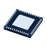
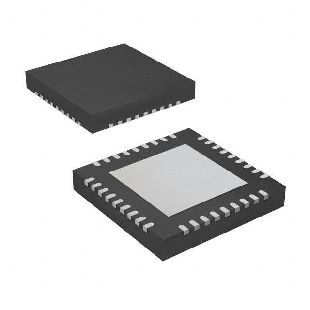
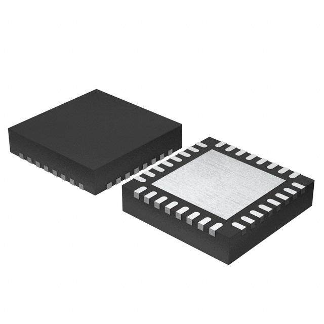
| 描述 | IC AUDIO CODEC 24BIT PCM 48VQFN接口—CODEC Lo-Pwr Stereo CODEC |
| 产品分类 | |
| 品牌 | Texas Instruments |
| 产品手册 | |
| 产品图片 |
|
| rohs | 符合RoHS无铅 / 符合限制有害物质指令(RoHS)规范要求 |
| 产品系列 | 接口 IC,接口—CODEC,Texas Instruments TLV320AIC3106IRGZT- |
| 数据手册 | |
| 产品型号 | TLV320AIC3106IRGZT |
| PCN封装 | |
| PCN设计/规格 | |
| THD+噪声 | - 89 dB ADC/- 95 dB DAC |
| 三角积分 | 是 |
| 产品种类 | 接口—CODEC |
| 供应商器件封装 | 48-VQFN(7x7) |
| 信噪比 | 92 dB ADC/102 dB DAC |
| 信噪比,ADC/DAC(db)(典型值) | 92 / 102 |
| 其它名称 | 296-31972-6 |
| 分辨率 | 24 bit |
| 分辨率(位) | 24 b |
| 动态范围,ADC/DAC(db)(典型值) | 91 / 92 |
| 包装 | Digi-Reel® |
| 单位重量 | 137.400 mg |
| 商标 | Texas Instruments |
| 安装类型 | 表面贴装 |
| 安装风格 | SMD/SMT |
| 封装 | Reel |
| 封装/外壳 | 48-VFQFN 裸露焊盘 |
| 封装/箱体 | VQFN-48 |
| 工作温度 | -40°C ~ 85°C |
| 工厂包装数量 | 250 |
| 接口类型 | Serial (I2C) |
| 数据接口 | PCM 音频接口 |
| 最大工作温度 | + 85 C |
| 最小工作温度 | - 40 C |
| 标准包装 | 1 |
| 电压-电源,数字 | 1.65 V ~ 1.95 V |
| 电压-电源,模拟 | 2.7 V ~ 3.6 V |
| 类型 | 立体声音频 |
| 系列 | TLV320AIC3106 |
| 转换速率 | 96 kHz |
| 配用 | /product-detail/zh/TLV320AIC3106EVM-K/296-31035-ND/1906858 |


- 商务部:美国ITC正式对集成电路等产品启动337调查
- 曝三星4nm工艺存在良率问题 高通将骁龙8 Gen1或转产台积电
- 太阳诱电将投资9.5亿元在常州建新厂生产MLCC 预计2023年完工
- 英特尔发布欧洲新工厂建设计划 深化IDM 2.0 战略
- 台积电先进制程称霸业界 有大客户加持明年业绩稳了
- 达到5530亿美元!SIA预计今年全球半导体销售额将创下新高
- 英特尔拟将自动驾驶子公司Mobileye上市 估值或超500亿美元
- 三星加码芯片和SET,合并消费电子和移动部门,撤换高东真等 CEO
- 三星电子宣布重大人事变动 还合并消费电子和移动部门
- 海关总署:前11个月进口集成电路产品价值2.52万亿元 增长14.8%


PDF Datasheet 数据手册内容提取
Product Sample & Technical Tools & Support & Folder Buy Documents Software Community TLV320AIC3106 SLAS509F–DECEMBER2006–REVISEDDECEMBER2014 TLV320AIC3106 Low-Power Stereo Audio CODEC for Portable Audio/Telephony 1 Features • ConcurrentDigitalMicrophoneandAnalog MicrophoneSupportAvailable • StereoAudioDAC 1 • ExtensiveModularPowerControl – 102-dBASignal-to-NoiseRatio • PowerSupplies: – 16/20/24/32-BitData – Analog:2.7V–3.6V. – SupportsRatesFrom8kHzto96kHz – DigitalCore:1.65V–1.95V – 3D/Bass/Treble/EQ/De-EmphasisEffects – DigitalI/O:1.1V–3.6V – FlexiblePowerSavingModesand Packages:5.00mm ×5.00mm80-pinVFBGA; PerformanceareAvailable 7.00mm×7.00mm48-pinQFN • StereoAudioADC – 92-dBASignal-to-NoiseRatio 2 Applications – SupportsRatesFrom8kHzto96kHz • DigitalCameras – DigitalSignalProcessingandNoiseFiltering • SmartCellularPhones AvailableDuringRecord • TenAudioInputPins 3 Description – ProgrammableinSingle-EndedorFully The TLV320AIC3106 is a low-power stereo audio DifferentialConfigurations codec with stereo headphone amplifier, as well as multiple inputs and outputs programmable in single- – 3-StateCapabilityforFloatingInput ended or fully differential configurations. Extensive Configurations register-based power control is included, enabling • SevenAudioOutputDrivers stereo 48-kHz DAC playback as low as 15 mW from – StereoFullyDifferentialorSingle-Ended a 3.3-V analog supply, making it ideal for portable HeadphoneDrivers battery-poweredaudioandtelephonyapplications. – FullyDifferentialStereoLineOutputs The record path of the TLV320AIC3106 contains – FullyDifferentialMonoOutput integrated microphone bias, digitally controlled stereo microphone preamplifier, and automatic gain control • LowPower:15-mWStereo48-kHzPlaybackWith (AGC), with mix/mux capability among the multiple 3.3-VAnalogSupply analog inputs. Programmable filters are available • Ultralow-PowerModewithPassiveAnalogBypass during record which can remove audible noise that • ProgrammableInput/OutputAnalogGains canoccurduringopticalzoomingindigitalcameras. • AutomaticGainControl(AGC)forRecord DeviceInformation(1) • ProgrammableMicrophoneBiasLevel PARTNUMBER PACKAGE BODYSIZE(NOM) • ProgrammablePLLforFlexibleClockGeneration BGAMICROSTAR • ControlBusSelectableSPIorI2C TLV320AIC3106 JUNIOR(80) 5.00mmx5.00mm • AudioSerialDataBusSupportsI2S,Left/Right- VQFN(48) 7.00mmx7.00mm Justified,DSP,andTDMModes (1) For all available packages, see the orderable addendum at • AlternateSerialPCM/I2SDataBusforEasy theendofthedatasheet. ConnectiontoBluetooth™Module 4 Simplified Diagram 1 An IMPORTANT NOTICE at the end of this data sheet addresses availability, warranty, changes, use in safety-critical applications, intellectualpropertymattersandotherimportantdisclaimers.PRODUCTIONDATA.
TLV320AIC3106 SLAS509F–DECEMBER2006–REVISEDDECEMBER2014 www.ti.com Table of Contents 1 Features.................................................................. 1 11.2 FunctionalBlockDiagram.....................................16 2 Applications........................................................... 1 11.3 FeatureDescription...............................................16 3 Description............................................................. 1 11.4 DeviceFunctionalModes......................................39 11.5 Programming.........................................................42 4 SimplifiedDiagram................................................ 1 11.6 RegisterMaps.......................................................46 5 RevisionHistory..................................................... 2 11.7 OutputStageVolumeControls.............................64 6 Description(continued)......................................... 3 12 ApplicationandImplementation........................ 91 7 DeviceComparisonTable..................................... 3 12.1 ApplicationInformation..........................................91 8 PinConfigurationandFunctions......................... 4 12.2 TypicalApplication ...............................................91 9 Specifications......................................................... 6 13 PowerSupplyRecommendations..................... 93 9.1 AbsoluteMaximumRatings......................................6 14 Layout................................................................... 94 9.2 ESDRatings..............................................................6 14.1 LayoutGuidelines.................................................94 9.3 RecommendedOperatingConditions.......................6 14.2 LayoutExample....................................................94 9.4 ThermalInformation..................................................7 15 DeviceandDocumentationSupport................. 96 9.5 ElectricalCharacteristics...........................................7 15.1 Trademarks...........................................................96 9.6 TimingRequirements:AudioDataSerialInterface.10 15.2 ElectrostaticDischargeCaution............................96 9.7 TypicalCharacteristics............................................13 15.3 Glossary................................................................96 10 ParameterMeasurementInformation................14 16 Mechanical,Packaging,andOrderable 11 DetailedDescription........................................... 15 Information........................................................... 96 11.1 Overview...............................................................15 5 Revision History ChangesfromRevisionE(December2008)toRevisionF Page • AddedESDRatingstable,FeatureDescriptionsection,DeviceFunctionalModes,ApplicationandImplementation section,PowerSupplyRecommendationssection,Layoutsection,andDeviceandDocumentationSupport ....................1 2 SubmitDocumentationFeedback Copyright©2006–2014,TexasInstrumentsIncorporated ProductFolderLinks:TLV320AIC3106
TLV320AIC3106 www.ti.com SLAS509F–DECEMBER2006–REVISEDDECEMBER2014 6 Description (continued) The playback path includes mix/mux capability from the stereo DAC and selected inputs, through programmable volumecontrols,tothevariousoutputs. The TLV320AIC3106 contains four high-power output drivers as well as three fully differential output drivers. The high-power output drivers are capable of driving a variety of load configurations, including up to four channels of single-ended 16-Ω headphones using ac-coupling capacitors, or stereo 16-Ω headphones in a capacitorless outputconfiguration. The stereo audio DAC supports sampling rates from 8 kHz to 96 kHz and includes programmable digital filtering in the DAC path for 3D, bass, treble, midrange effects, speaker equalization, and de-emphasis for 32-kHz, 44.1- kHz, and 48-kHz rates. The stereo audio ADC supports sampling rates from 8 kHz to 96 kHz and is preceded by programmable gain amplifiers or AGC that can provide up to 59.5-dB analog gain for low-level microphone inputs. The TLV320AIC3106 provides an extremely high range of programmability for both attack (8 ms–1,408 ms) and for decay (0.05 s–22.4 s). This extended AGC range allows the AGC to be tuned for many types of applications. For battery saving applications where neither analog nor digital signal processing are required, the device can be putinaspecialanalogsignalpassthrumode.Thismodesignificantlyreducespowerconsumption,asmostofthe deviceispowereddownduringthispassthroughoperation. The serial control bus supports SPI or I2C protocols, while the serial audio data bus is programmable for I2S, left/right-justified, DSP, or TDM modes. A highly programmable PLL is included for flexible clock generation and supportforallstandardaudioratesfromawiderangeofavailableMCLKs,varyingfrom512kHzto50MHz,with special attention paid to the most popular cases of 12-MHz, 13-MHz, 16-MHz, 19.2-MHz, and 19.68-MHz system clocks. The TLV320AIC3106 operates from an analog supply of 2.7 V–3.6 V, a digital core supply of 1.65 V–1.95 V, and a digital I/O supply of 1.1 V–3.6 V. The device is available in the 5-mm × 5-mm, 80-ball MicroStar Junior™ BGA packageanda7-mm× 7-mm,48-leadQFNpackage. 7 Device Comparison Table DEVICENAME DESCRIPTION TLV320AIC3106 Low-PowerStereoCODECwith10Inputs,7Outputs,Speaker/HPAmpandEnhancedDigitalEffects. TLV320AIC3101 SameasTLV320AIC3106,butwith6inputs,6outputsandSpeaker/HPAmp. TLV320AIC3104 SameasTLV320AIC3106,butwith6inputsand6outputs. TLV320AIC3105 SameasTLV320AIC3106,butwith6Single-endedinputsand6outputs. TLV320AIC3107 SameasTLV320AIC3106,butwith7Inputs,6OutputsandIntegratedMonoClass-DAmplifier. Copyright©2006–2014,TexasInstrumentsIncorporated SubmitDocumentationFeedback 3 ProductFolderLinks:TLV320AIC3106
TLV320AIC3106 SLAS509F–DECEMBER2006–REVISEDDECEMBER2014 www.ti.com 8 Pin Configuration and Functions RGZ48-PinPackage (BottomView) ZQE80-BallPackage (BottomView) 1 1 2 J 4 8 1 3 H G F E D C B A 3 7 2 4 1 2 3 4 5 6 7 8 9 3 6 2 5 Theshadedballsarenotconnectedtothe SoldertheQFNthermalpadtotheground die,butareelectricallyconnectedtoeach plane(DRVSS). other.Isrecommendedtosolderthemto analoggroundinordertoenhancethe thermalperformanceofthedevice. PinFunctions PIN I/O DESCRIPTION NAME QFN BGABALL MICBIAS 13 A2 O Microphonebiasvoltageoutput MIC3R 14 A1 I MIC3input(rightormultifunction) AVSS_ADC 15 C2,D2 – AnalogADCgroundsupply,0V DRVDD 16,17 B1,C1 – ADCanalogandoutputdrivervoltagesupply,2.7V–3.6V HPLOUT 18 D1 O High-poweroutputdriver(left+) HPLCOM 19 E1 O High-poweroutputdriver(left–ormultifunctional) DRVSS 20,21 E2,F2 – Analogoutputdrivergroundsupply,0V HPRCOM 22 F1 O High-poweroutputdriver(right–ormultifunctional) HPROUT 23 G1 O High-poweroutputdriver(right+) DRVDD 24 H1 – ADCanalogandoutputdrivervoltagesupply,2.7V–3.6V AVDD_DAC 25 J1 – AnalogDACvoltagesupply,2.7V–3.6V AVSS_DAC 26 G2,H2 – AnalogDACgroundsupply,0V MONO_LOP 27 J2 O Monolineoutput(+) MONO_LOM 28 J3 O Monolineoutput(–) LEFT_LOP 29 J4 O Leftlineoutput(+) LEFT_LOM 30 J5 O Leftlineoutput(–) RIGHT_LOP 31 J6 O Rightlineoutput(+) RIGHT_LOM 32 J7 O Rightlineoutput(–) RESET 33 H8 I Reset General-purposeinput/output#2(input/output)/digitalmicrophonedatainput/PLLclock GPIO2 34 J8 I/O input/audioserialdatabusbitclockinput/output 4 SubmitDocumentationFeedback Copyright©2006–2014,TexasInstrumentsIncorporated ProductFolderLinks:TLV320AIC3106
TLV320AIC3106 www.ti.com SLAS509F–DECEMBER2006–REVISEDDECEMBER2014 PinFunctions(continued) PIN I/O DESCRIPTION NAME QFN BGABALL General-purposeinput/output#1(input/output)/PLL/clockmuxoutput/shortcircuit GPIO1 35 J9 I/O interrupt/AGCnoiseflag/digitalmicrophoneclockaudioserialdatabuswordclock input/output DVDD 36 H9 – Digitalcorevoltagesupply,1.65V–1.95V MCLK 37 G8 I Masterclockinput BCLK 38 G9 I Audioserialdatabusbitclock(input/output) WCLK 39 F9 I Audioserialdatabuswordclock(input/output) DIN 40 E9 I Audioserialdatabusdatainput(input) DOUT 41 F8 O Audioserialdatabusdataoutput(output) DVSS 42 D9 – Digitalcore/I/Ogroundsupply,0V SELECT 43 E8 I Controlmodeselectpin(1=SPI,0=I2C) IOVDD 44 C9 – I/Ovoltagesupply,1.1V–3.6V MFP0 45 B8 I Multifunctionpin#0–SPIchipselect/GPI/I2Caddresspin#0 MFP1 46 B9 I Multifunctionpin#1–SPIserialclock/GPI/I2Caddresspin#1S MFP2 47 A8 I Multifunctionpin#2–SPIMISOslaveserialdataoutput/GPOI Multifunctionpin#3–SPIMOSIslaveserialdatainput/GPI/audioserialdatabusdata MFP3 48 A9 I input SCL 1 C8 I/O I2Cserialclock/GPIO SDA 2 D8 I/O I2Cserialdatainput/output/GPIO NC – A7 – Notconnected LINE1LP 3 A6 I MIC1orLine1analoginput(left+ormultifunction) LINE1LM 4 A5 I MIC1orLine1analoginput(left–ormultifunction) LINE1RP 5 B7 I MIC1orLine1analoginput(right+ormultifunction) LINE1RM 6 B6 I MIC1orLine1analoginput(right–ormultifunction) LINE2LP 7 A4 I MIC2orLine2analoginput(left+ormultifunction) LINE2LM 8 B5 I MIC2orLine2analoginput(left–ormultifunction) LINE2RP 9 B4 I MIC2orLine2analoginput(right+ormultifunction) LINE2RM 10 A3 I MIC2orLine2analoginput(right–ormultifunction) MIC3L 11 B3 I MIC3input(leftormultifunction) MICDET 12 B2 I Microphonedetect C4-C7, D3-D7, E3-E7, NC – – Notconnected F3-F7, G3-G7, H3-H7 Copyright©2006–2014,TexasInstrumentsIncorporated SubmitDocumentationFeedback 5 ProductFolderLinks:TLV320AIC3106
TLV320AIC3106 SLAS509F–DECEMBER2006–REVISEDDECEMBER2014 www.ti.com 9 Specifications 9.1 Absolute Maximum Ratings overoperatingfree-airtemperaturerange(unlessotherwisenoted)(1) (2) MIN MAX. UNIT AVDD_DACtoAVSS_DAC,DRVDDtoDRVSS, –0.3 3.9 V AVSS_ADC AVDDtoDRVSS –0.3 3.9 V Inputvoltage IOVDDtoDVSS –0.3 3.9 V DVDDtoDVSS –0.3 2.5 V AVDD_DACtoDRVDD –0.1 0.1 V Digitalinputvoltage toDVSS –0.3 IOVDD+0.3 V Analoginputvoltage toAVSS_ADC –0.3 AVDD+0.3 V Operatingtemperature –40 t85 °C Junctiontemperature,T 105 °C J Storagetemperature,T –65 105 °C stg Powerdissipation (T Max–T )/θ J A JA (1) Stressesbeyondthoselistedunderabsolutemaximumratingsmaycausepermanentdamagetothedevice.Thesearestressratings only,andfunctionaloperationofthedeviceattheseoranyotherconditionsbeyondthoseindicatedunderrecommendedoperating conditionsisnotimplied.Exposuretoabsolute-maximum-ratedconditionsforextendedperiodsmayaffectdevicereliability. (2) ESDcomplicancetestedtoEIA/JESD22-A114-Bandpassed. 9.2 ESD Ratings VALUE UNIT Human-bodymodel(HBM),perANSI/ESDA/JEDECJS-001(1) ±1900 V(ESD) Electrostaticdischarge Charged-devicemodel(CDM),perJEDECspecificationJESD22- V C101(2) ±1500 (1) JEDECdocumentJEP155statesthat500-VHBMallowssafemanufacturingwithastandardESDcontrolprocess. (2) JEDECdocumentJEP157statesthat250-VCDMallowssafemanufacturingwithastandardESDcontrolprocess. 9.3 Recommended Operating Conditions overoperatingfree-airtemperaturerange(unlessotherwisenoted) MIN NOM MAX UNIT AVDD_DAC,DRVDD(1) Analogsupplyvoltage 2.7 3.3 3.6 V DVDD(1) Digitalcoresupplyvoltage 1.65 1.8 1.95 V IOVDD(1) DigitalI/Osupplyvoltage 1.1 1.8 3.6 V V Analogfull-scale0-dBinputvoltage(DRVDD1=3.3V) 0.707 V I RMS Stereolineoutputloadresistance 10 kΩ Stereoheadphoneoutputloadresistance 16 Ω Digitaloutputloadcapacitance 10 pF T Operatingfree-airtemperature –40 85 °C A (1) AnalogvoltagevaluesarewithrespecttoAVSS_ADC,AVSS_DAC,DRVSS;digitalvoltagevaluesarewithrespecttoDVSS. 6 SubmitDocumentationFeedback Copyright©2006–2014,TexasInstrumentsIncorporated ProductFolderLinks:TLV320AIC3106
TLV320AIC3106 www.ti.com SLAS509F–DECEMBER2006–REVISEDDECEMBER2014 9.4 Thermal Information RGZ ZQE THERMALMETRIC(1) UNIT 48PINS 80PINS R Junction-to-ambientthermalresistance 26.1 54.3 θJA R Junction-to-case(top)thermalresistance 12.7 25.7 θJC(top) R Junction-to-boardthermalresistance 3.9 31.8 θJB °C/W ψ Junction-to-topcharacterizationparameter 0.2 0.5 JT ψ Junction-to-boardcharacterizationparameter 3.4 31.8 JB R Junction-to-case(bottom)thermalresistance 0.4 N/A θJC(bot) (1) Formoreinformationabouttraditionalandnewthermalmetrics,seetheICPackageThermalMetricsapplicationreport,SPRA953. 9.5 Electrical Characteristics At25°C,AVDD_DAC,DRVDD,IOVDD=3.3V,DVDD=1.8V,f =48-kHz,16-bitaudiodata(unlessotherwisenoted) S PARAMETER TESTCONDITIONS MIN TYP MAX UNIT AUDIOADC Inputsignallevel(0-dB) Single-endedinput 0.707 VRMS Signal-to-noiseratio,A-weighted(1)(2) fS=48ksps,0-dBPGAgain,inputsac-shortedtoground 80 92 dB Dynamicrange(2) fS=48ksps,0-dBPGAgain,–60dBfull-scaleinputsignal 91 dB THD Totalharmonicdistortion fS=48ksps,0-dBPGAgain,–2dBfull-scale,1-kHzinputsignal –88 –70 dB 217-HzsignalappliedtoDRVDD 49 PSRR Powersupplyrejectionratio dB 1-kHzsignalappliedtoDRVDD 46 Gainerror fS=48ksps,0-dBPGAgain,–2dBfull-scale,1-kHzinputsignal 0.84 dB 1-kHz,–2-dBfull-scalesignal,MIC3LtoMIC3R –86 Inputchannelseparation 1-kHz,–2-dBfull-scalesignal,MIC2LtoMIC2R –98 dB 1-kHz,–2-dBfull-scalesignal,MIC1LtoMIC1R –75 ADCprogrammablegainamplifier 1-kHzinputtone 59.5 dB maximumgain ADCprogrammablegainamplifierstep 0.5 dB size MIC1L/MIC1RinputsroutedtosingleADC 20 Inputmixattenuation=0dB MIC1L/MIC1RinputsroutedtosingleADC,inputmixattenuation=12dB 80 MIC2L/MIC2RinputsroutedtosingleADC 20 Inputresistance Inputmixattenuation=0dB kΩ MIC2L/MIC2RinputsroutedtosingleADC,inputmixattenuation=12dB 80 MIC3L/MIC3RinputsroutedtosingleADC 20 Inputmixattenuation=0dB MIC3L/MIC3RinputsroutedtosingleADC,inputmixattenuation=12dB 80 Inputlevelcontrolminimumattenuation 0 dB setting Inputlevelcontrolmaximumattenuation 12 dB setting Inputsignallevel DifferentialInput 1.414 VRMS Signal-to-noiseratio,A-weighted(1)(2) fS=48ksps,0-dBPGAgain,inputsac-shortedtoground, 92 dB differentialmode THD Totalharmonicdistortion fS=48ksps,0-dBPGAgain,–2-dBfull-scale1-kHzinputsignal,differential –91 dB mode (1) Ratioofoutputlevelwith1-kHzfull-scalesine-waveinput,totheoutputlevelwiththeinputsshortcircuited,measuredA-weightedovera 20-Hzto20-kHzbandwidthusinganaudioanalyzer. (2) Allperformancemeasurementsdonewith20-kHzlow-passfilterand,wherenoted,A-weightedfilter.Failuretousesuchafiltermay resultinhigherTHD+NandlowerSNRanddynamicrangereadingsthanshownintheElectricalCharacteristics.Thelow-passfilter removesout-of-bandnoise,which,althoughnotaudible,mayaffectdynamicspecificationvalues. Copyright©2006–2014,TexasInstrumentsIncorporated SubmitDocumentationFeedback 7 ProductFolderLinks:TLV320AIC3106
TLV320AIC3106 SLAS509F–DECEMBER2006–REVISEDDECEMBER2014 www.ti.com Electrical Characteristics (continued) At25°C,AVDD_DAC,DRVDD,IOVDD=3.3V,DVDD=1.8V,f =48-kHz,16-bitaudiodata(unlessotherwisenoted) S PARAMETER TESTCONDITIONS MIN TYP MAX UNIT ANALOGPASSTHROUGHMODE MIC1/LINE1toLINE_OUT 330 Inputtooutputswitchresistance,(rdsON) MIC2/LINE2toLINE_OUT 330 Ω ADCDIGITALDECIMATIONFILTER,fS=48kHz Filtergainfrom0to0.39fS ±0.1 dB Filtergainat0.4125fS –0.25 dB Filtergainat0.45fS –3 dB Filtergainat0.5fS –17.5 dB Filtergainfrom0.55fSto64fS –75 dB Filtergroupdelay 17/fS s MICROPHONEBIAS Programmablesetting=2.0 2.0 Biasvoltage Programmablesetting=2.5 2.3 2.5 2.7 V Programmablesetting=DRVDD DRVDD Currentsourcing Programmablesetting=2.5V 4 mA AUDIODAC–DifferentialLineoutput,load=10kΩ 0-dBinputfull-scalesignal,outputvolumecontrol=0dB,outputcommon- Full-scaleoutputvoltage modesetting=1.35V 1.414 VRMS SNR Signal-to-noiseratio,A-weighted(3) Noinputsignal,outputvolumecontrol=0dB,outputcommonmode 90 102 dB setting=1.35V,fS=48kHz –60dB1-kHzinputfull-scalesignal,outputvolumecontrol=0dB,output Dynamicrange,A-weighted 99 dB common-modesetting=1.35V,fS=48kHz 0-dB1-kHzinputfull-scalesignal,outputvolumecontrol=0dB,output THD Totalharmonicdistortion –94 –75 dB common-modesetting=1.35V,fS=48kHz 217-HzsignalappliedtoDRVDD,AVDD_DAC 77 Power-supplyrejectionratio dB 1-kHzsignalappliedtoDRVDD,AVDD_DAC 73 DACchannelseparation 0-dBfull-scaleinputsignalbetweenleftandrightLineout 123 dB 0-dB1-kHzinputfull-scalesignal,outputvolumecontrol=0dB,output DACgainerror –0.4 dB common-modesetting=1.35V,fS=48kHz AUDIODAC–SINGLEENDEDLINEOUTPUT,Load=10kΩ 0-dBinputfull-scalesignal,outputvolumecontrol=0dB,outputcommon- Full-scaleoutputvoltage modesetting=1.35V 0.707 VRMS Noinputsignal,outputvolumecontrol=0dB,outputcommon-mode SNR Signal-to-noiseratio,A-weighted 97 dB setting=1.35V,fS=48kHz 0-dB1-kHzinputfull-scalesignal,outputvolumecontrol=0dB,output THD Totalharmonicdistortion 84 dB common-modesetting=1.35V,fS=48kHz 0-dB1-kHzinputfull-scalesignal,outputvolumecontrol=0dB,output DACgainerror 0.55 dB common-modesetting=1.35V,fS=48kHz AUDIODAC–SINGLEENDEDHEADPHONEOUTPUT,Load=16Ω 0-dBinputfull-scalesignal,outputvolumecontrol=0dB,outputcommon- Full-scaleoutputvoltage modesetting=1.35V 0.707 VRMS Noinputsignal,outputvolumecontrol=0dB,outputcommon-mode 95 dB SNR Signal-to-noiseratio,A-weighted setting=1.35V,fS=48kHz Noinputsignal,outputvolumecontrol=0dB,outputcommon-mode 96 dB setting=1.35V,fS=48kHz,50%DACcurrentboostmode –60-dB1-kHzinputfull-scalesignal,outputvolumecontrol=0dB,output Dynamicrange,A-weighted 92 dB common-modesetting=1.35V,fS=48kHz 0-dB1-kHzinputfull-scalesignal,outputvolumecontrol=0dB,output THD Totalharmonicdistortion –80 –65 dB common-modesetting=1.35V,fS=48kHz 217-HzsignalappliedtoDRVDD,AVDD_DAC 41 PSRR Power-supplyrejectionratio dB 1-kHzsignalappliedtoDRVDD,AVDD_DAC 44 DACchannelseparation 0-dBfull-scaleinputsignalbetweenleftandrightLineout 84 dB 0-dB1-kHzinputfull-scalesignal,outputvolumecontrol=0dB,output DACgainerror –0.5 dB common-modesetting=1.35V,fS=48kHz (3) Unlessotherwisenoted,allmeasurementsuseoutputcommon-modevoltagesettingof1.35V,0-dBoutputlevelcontrolgain,16-Ω single-endedload. 8 SubmitDocumentationFeedback Copyright©2006–2014,TexasInstrumentsIncorporated ProductFolderLinks:TLV320AIC3106
TLV320AIC3106 www.ti.com SLAS509F–DECEMBER2006–REVISEDDECEMBER2014 Electrical Characteristics (continued) At25°C,AVDD_DAC,DRVDD,IOVDD=3.3V,DVDD=1.8V,f =48-kHz,16-bitaudiodata(unlessotherwisenoted) S PARAMETER TESTCONDITIONS MIN TYP MAX UNIT AUDIODAC–LINEOUTANDHEADPHONEOUTDRIVERS Firstoption 1.35 Secondoption 1.5 Outputcommonmode V Thirdoption 1.65 Fourthoption 1.8 Outputvolumecontrolmaxsetting 9 dB Outputvolumecontrolstepsize 1 dB DACDIGITALINTERPOLATION–FILTERfS=48ksps Passband 0 0.45fS Hz Pass-bandripple ±0.06 dB Transitionband 0.45fS 0.55fS Hz Stopband 0.55fS 7.5fS Hz Stop-bandattenuation 65 dB Groupdelay 21/fS s DIGITALI/O VIL Inputlowlevel –0.3 0.3×IOVDD V 0.7× IOVDD>1.6V VIH Inputhighlevel(4) IOVDD V IOVDD<1.6V 1.1 VOL Outputlowlevel 0.1×IOVDD V 0.8× VOH Outputhighlevel IOVDD V POWERCONSUMPTION,DRVDD,AVDD_DAC=3.3V,DVDD=1.8V,IOVDD=3.3V IDRVDD+IAVDD_DAC 0.1 RESETheldlow μA IDVDD 0.2 IDRVDD+IAVDD_DAC 2.1 mA IDVDD MonoADCrecord,fS=8ksps,I2Sslave,AGC 0.5 IDRVDD+IAVDD_DAC off,nosignal 4.1 mA IDVDD 0.6 IDRVDD+IAVDD_DAC StereoADCrecord,fS=48ksps,I2Sslave, 4.3 mA IDVDD AGCoff,nosignal 2.5 IDRVDD+IAVDD_DAC StereoDACplaybacktoLineout,analogmixer 3.5 mA IDVDD bypassed,fS=48ksps,I2Sslave 2.3 IDRVDD+IAVDD_DAC StereoDACplaybacktoLineout,fS=48ksps, 4.9 mA IDVDD I2Sslave,nosignal 2.3 IDRVDD+IAVDD_DAC StereoDACplaybacktostereosingle-ended 6.7 mA IDVDD headphone,fS=48ksps,I2Sslave,nosignal 2.3 IDRVDD+IAVDD_DAC 3.1 StereoLineintostereoLineout,nosignal mA IDVDD 0 IDRVDD+IAVDD_DAC 1.4 ExtrapowerwhenPLLenabled mA IDVDD 0.9 IDRVDD+IAVDD_DAC Allblockspowereddown,headsetdetedtion 28 μA IDVDD enabled 2 (4) WhenIOVDD<1.6V,minimumV is1.1V. IH Copyright©2006–2014,TexasInstrumentsIncorporated SubmitDocumentationFeedback 9 ProductFolderLinks:TLV320AIC3106
TLV320AIC3106 SLAS509F–DECEMBER2006–REVISEDDECEMBER2014 www.ti.com 9.6 Timing Requirements: Audio Data Serial Interface(1) IOVDD=1.1V IOVDD=3.3V PARAMETER UNIT MIN MAX MIN MAX I2S/LJF/RJFTiminginMasterMode t (WS) ADWS/WCLKdelaytime 50 15 ns d t (DO-WS) ADWS/WCLKtoDOUTdelaytime 50 20 ns d t (DO-BCLK) BCLKtoDOUTdelaytime 50 15 ns d t(DI) DINsetuptime 10 6 ns s t (DI) DINholdtime 10 6 ns h t Risetime 30 10 ns r t Falltime 30 10 ns f DSPTiminginMasterMode t (WS) ADWS/WCLKdelaytime 50 15 ns d t (DO-BCLK) BCLKtoDOUTdelaytime 50 15 ns d t(DI) DINsetuptime 10 6 ns s t (DI) DINholdtime 10 6 ns h t Risetime 30 10 ns r t Falltime 30 10 ns f I2S/LJF/RJFTiminginSlaveMode t (BCLK) BCLKhighperiod 70 35 ns H t (BCLK) BCLKlowperiod 70 35 ns L t(WS) ADWS/WCLKsetuptime 10 6 ns s t (WS) ADWS/WCLKholdtime 10 6 ns h t (DO-WS) ADWS/WCLKtoDOUTdelaytime(forLJFModeonly) 50 35 ns d t (DO-BCLK) BCLKtoDOUTdelaytime 50 20 ns d t(DI) DINsetuptime 10 6 ns s t (DI) DINholdtime 10 6 ns h t Risetime 8 4 ns r t Falltime 8 4 ns f DSPTiminginSlaveMode t (BCLK) BCLKhighperiod 70 35 ns H t (BCLK) BCLKlowperiod 70 35 ns L t(WS) ADWS/WCLKsetuptime 10 8 ns s t (WS) ADWS/WCLKholdtime 10 8 ns h t (DO-BCLK) BCLKtoDOUTdelaytime 50 20 ns d t(DI) DINsetuptime 10 6 ns s t (DI) DINholdtime 10 6 ns h t Risetime 8 4 ns r t Falltime 8 4 ns f (1) Alltimingspecificationsaremeasuredatcharacterizationbutnottestedatfinaltest. 10 SubmitDocumentationFeedback Copyright©2006–2014,TexasInstrumentsIncorporated ProductFolderLinks:TLV320AIC3106
TLV320AIC3106 www.ti.com SLAS509F–DECEMBER2006–REVISEDDECEMBER2014 WCLK t(WS) d BCLK t(DO-WS) t(DO-BCLK) d d SDOUT t (DI) t(DI) S h SDIN T0145-01 Allspecificationsat25°C,DVDD=1.8V. Figure1. I2S/LJF/RJFTiminginMasterMode WCLK t(WS) t(WS) d d BCLK t(DO-BCLK) d SDOUT t (DI) t(DI) S h SDIN T0146-01 Figure2. DSPTiminginMasterMode Copyright©2006–2014,TexasInstrumentsIncorporated SubmitDocumentationFeedback 11 ProductFolderLinks:TLV320AIC3106
TLV320AIC3106 SLAS509F–DECEMBER2006–REVISEDDECEMBER2014 www.ti.com WCLK t (WS) S t(WS) h t (BCLK) H BCLK t(BCLK) t(DO-WS) L d t(DO-BCLK) d SDOUT t (DI) t(DI) S h SDIN T0145-02 Figure3. I2S/LJF/RJFTiminginSlaveMode WCLK t (WS) t (WS) S S t(WS) t(WS) h h t(BCLK) L BCLK t (BCLK) t(DO-BCLK) H d SDOUT t (DI) t(DI) S h SDIN T0146-02 Figure4. DSPTiminginSlaveMode 12 SubmitDocumentationFeedback Copyright©2006–2014,TexasInstrumentsIncorporated ProductFolderLinks:TLV320AIC3106
TLV320AIC3106 www.ti.com SLAS509F–DECEMBER2006–REVISEDDECEMBER2014 9.7 Typical Characteristics 0 45 2.7 VDD_CM 1.35_LDAC -10 40 B 3.6 VDD_CM 1.8_LDAC stortion - d --3200 23.7.3 V DVDD_DC_MCM 11.3.655__RLDDAACC Noise - dB 3305 c Di -40 To- 25 moni -50 3.3 VDD_CM 1.65_RDAC gnal- 20 ar Si al H -60 R - 15 Tot SN HD - -70 10 LINEIR Routed to RADC in Differential Mode, T 48 KSPS, Normal Supply and Temperature, -80 3.6 VDD_CM 1.8_RDAC 5 Input Signal at -65 dB -90 0 0 20 40 60 80 100 0 10 20 30 40 50 60 70 Headphone Out Power - mW ADC, PGA- Setting - dB Figure5.TotalHarmonicDistortionvsHeadphoneOut Figure6.Signal-To-NoiseRatiovsADCPGASetting Power 4 4 AVDD= 3.3 V, No Load No Load V 3.5 PGM = VDD 3.5 PGM = VDD - V GE E - OLTA 3 OLTAG 3 SV PGM = 2.5 V S V PGM = 2.5 V BIA 2.5 BIA 2.5 C C MI MI PGM = 2 V PGM = 2 V 2 2 1.5 1.5 2.7 2.9 3.1 3.3 3.5 -60 -40 -20 0 20 40 60 80 100 VDD- Supply Voltage - V TA- Free-Air Temperature - °C Figure7.MICBIASVoltagevsSupplyVoltage Figure8.MICBIASVoltagevsFree-AirTemperature 0 0 Load = 10 kW, Load = 10 kW, -20 F40S9 =6 4S8a mkHpzle, sfs,= 64 kHz, -20 FS = 48 kHz, fs= 64 kHz, AVDD= DRVDD= 3.3 V, AVDD= DRVDD= 3.3 V, -40 -40 B B d -60 d -60 e - e - d d u -80 u -80 plit plit m m A-100 A-100 -120 -120 -140 -140 -160 -160 0 2 4 6 8 10 12 14 16 18 20 0 2 4 6 8 10 12 14 16 18 20 f - Frequency - kHz f - Frequency - kHz Figure9.LeftDACFFT Figure10.RightDACFFT Copyright©2006–2014,TexasInstrumentsIncorporated SubmitDocumentationFeedback 13 ProductFolderLinks:TLV320AIC3106
TLV320AIC3106 SLAS509F–DECEMBER2006–REVISEDDECEMBER2014 www.ti.com Typical Characteristics (continued) 0 0 Load = 10 kW, Load = 10 kW, -20 F20S4 =8 4S8a mkHpzle, sfs,= 64 kHz, -20 F20S4 =8 4S8a mkHpzle, sfs,= 64 kHz, AVDD= DRVDD= 3.3 V, AVDD= DRVDD= 3.3 V, -40 -40 B B d -60 d -60 e - e - d d u -80 u -80 plit plit m m A-100 A-100 -120 -120 -140 -140 -160 -160 0 2 4 6 8 10 12 14 16 18 20 0 2 4 6 8 10 12 14 16 18 20 f - Frequency - kHz f - Frequency - kHz Figure11.LeftADCFFT Figure12.RightADCFFT 10 Parameter Measurement Information AllparametersaremeasuredaccordingtotheconditionsdescribedintheSpecificationssection. 14 SubmitDocumentationFeedback Copyright©2006–2014,TexasInstrumentsIncorporated ProductFolderLinks:TLV320AIC3106
TLV320AIC3106 www.ti.com SLAS509F–DECEMBER2006–REVISEDDECEMBER2014 11 Detailed Description 11.1 Overview The TLV320AIC3106 is a highly flexible, low power, stereo audio codec with extensive feature integration, intended for applications in smartphones, PDAs, and portable computing, communication, and entertainment applications. Available in a 5x5mm 80-ball BGA (with 51 balls actually used) and 7x7mm 48-lead QFN, the product integrates a host of features to reduce cost, board space, and power consumption in space-constrained, battery-powered,portableapplications. TheTLV320AIC3106consistsofthefollowingblocks: • Stereoaudiomulti-bitdelta-sigmaDAC(8kHz–96kHz) • Stereoaudiomulti-bitdelta-sigmaADC(8kHz–96kHz) • Programmabledigitalaudioeffectsprocessing(3-D,bass,treble,mid-range,EQ,notchfilter,de-emphasis) • Sixaudioinputs • Fourhigh-poweraudiooutputdrivers(headphonedrivecapability) • Threefullydifferentiallineoutputdrivers • FullyprogrammablePLL • Headphone/headsetjackdetectionwithinterrupt Communication to the TLV320AIC3106 for control is pin-selectable (using the SELECT pin) as either SPI or I2C. The SPI interface requires that the Slave Select signal (MFP0) be driven low to communicate with the TLV320AIC3106. Data is then shifted into or out of the TLV320AIC3106 under control of the host microprocessor, which also provides the serial data clock. The I2C interface supports both standard and fast communication modes, and also enables cascading of up to four multiple codecs on the same I2C bus through theuseoftwopinsforaddressing(MFP0,MFP1). Copyright©2006–2014,TexasInstrumentsIncorporated SubmitDocumentationFeedback 15 ProductFolderLinks:TLV320AIC3106
TLV320AIC3106 SLAS509F–DECEMBER2006–REVISEDDECEMBER2014 www.ti.com 11.2 Functional Block Diagram DINDOUT BCLKWCLK LINE2LP MMICI2CL2MLP / /L LININEE22LLMP + HPLOUT LINE2LM Audio Serial Bus Interface MIC3L/ LINE3L AGC DOUTL DOUTR DINRDINL VCM HPLCOM + SW-D2 LINE1LP MMICIC1L1MLP // LLIINNEE11LLMP + 00.5/+dP5BG9 s.A5tedpBs ADC Effects VCoolunmtroel DALC SW-D1 + LINE1LM HPRCOM VCM + HPROUT AGC SW-D4 LINE1RP LINE2LP SW-L2 MMICIC1R1RMP // LLIINNEE11RRMP LINE1RM + 00.5/+dP5BG9 s.A5tedpBs ADC SW-D3 Effects VCoolnutmroel DACR + LINE1LP SSSWWW---LLL310 LEFT_LOP LEFT_LOM SW-L4 LINE1LM SW-L5 LINE2LM MIC3R / LINE3R SW-R2 LINE2RP SW-R1 LINE1RP SW-R0 LINE2RP + RIGHT_LOP SW-R3 MIC2RP/ LINE2RP RIGHT_LOM MIC2RM / LINE2RM LINE1RM SW-R4 SW-R5 LINE2RM LINE2RM Voltage Supplies ReBfeiraesn/ce AGuednioe rCaltoiocnk SPI / I2C Serial Control Bus + MONO_LOP MONO_LOM CDA_DDVACDA_SSVACAD_DDVACAD_SSVA DDVRDDDVRDSSVRDSSVRD DDVDDDVOISSVD TEDICM SAIBCIM KLCM 1_OIPG2_IOPG TESER TCELES 0RDA_C2/ILESC1RDA_CI2/KLCS OIP/GISOMOIPG/OSIMIOPG/LCSOIPG/ADS 11.3 Feature Description 11.3.1 HardwareReset The TLV320AIC3106 requires a hardware reset after power-up for proper operation. After all power supplies are at their specified values, the RESET pin must be driven low for at least 10 ns. If this reset sequence is not performed,theTLV320AIC3106maynotrespondproperlytoregisterreads/writes. 11.3.2 DigitalAudioDataSerialInterface Audio data is transferred between the host processor and the TLV320AIC3106 via the digital audio data serial interface, or audio bus. The audio bus on this device is very flexible, including left or right justified data options, support for I2S or PCM protocols, programmable data length options, a TDM mode for multichannel operation, very flexible master/slave configurability for each bus clock line, and the ability to communicate with multiple deviceswithinasystemdirectly. The data serial interface uses two sets of pins for communication between external devices, with the particular pinusedcontrolledthroughregisterprogramming.ThisconfigurationisshowninFigure13below. 16 SubmitDocumentationFeedback Copyright©2006–2014,TexasInstrumentsIncorporated ProductFolderLinks:TLV320AIC3106
TLV320AIC3106 www.ti.com SLAS509F–DECEMBER2006–REVISEDDECEMBER2014 Feature Description (continued) WCLK BCLK DIN DOUT GPIO1 GPIO2 MFP3 Audio Serial Data Bus Figure13. AlternateAudioBusMulitplexingFunction In cases where MFP3 is needed for a secondary device digital input, the TLV320AIC3106 must be used in I2C mode (when in SPI mode, MFP3 is used as the SPI bus MOSI pin and thus cannot be used here as an alternate digitalinputsource). This mux capability allows the TLV320AIC3106 to communicate with two separate devices with independent I2S/PCM buses. An example of such an application is a cellphone containing a Bluetooth transceiver with PCM/I2S interface, as shown in Figure 14. The applications processor can be connected to the WCLK, BCLK, DIN, DOUT pins on the TLV320AIC3106, while a Bluetooth device with PCM interface can be connected to the GPIO1, GPIO2, MFP3, and DOUT pins on the TLV320AIC3106. By programming the registers via I2C control, the applications processor can determine which device is communicating with the TLV320AIC3106. This is attractive in cases where the TLV320AIC3106 can be configured to communicate data with the Bluetooth device, then the applications processor can be put into a low power sleep mode, while voice/audio transmission still occursbetweentheBluetoothdeviceandtheTLV320AIC3106. Processor Processor 1 2 K K N T 3 1 2 WCL BCL DI DOU MFP GPIO GPIO AIC3106 Possible ProcessorTypes: Application Processor, Multimedia Processor, CompressedAudio Decoder, Wireless Modem, Bluetooth Module,AdditionalAudio/Voice Codec Figure14. TLV320AIC3106ConnectedtoMultipleAudioDevices Copyright©2006–2014,TexasInstrumentsIncorporated SubmitDocumentationFeedback 17 ProductFolderLinks:TLV320AIC3106
TLV320AIC3106 SLAS509F–DECEMBER2006–REVISEDDECEMBER2014 www.ti.com Feature Description (continued) The audio bus of the TLV320AIC3106 can be configured for left or right justified, I2S, DSP, or TDM modes of operation, where communication with standard telephony PCM interfaces is supported within the TDM mode. These modes are all MSB-first, with data width programmable as 16, 20, 24, or 32 bits. In addition, the word clock (WCLK or GPIO1) and bit clock (BCLK or GPIO2) can be independently configured in either Master or Slavemode,forflexibleconnectivitytoawidevarietyofprocessors The word clock (WCLK or GPIO1) is used to define the beginning of a frame, and may be programmed as either a pulse or a square-wave signal. The frequency of this clock corresponds to the maximum of the selected ADC andDACsamplingfrequencies. The bit clock (BCLK or GPIO2) is used to clock in and out the digital audio data across the serial bus. When in Master mode, this signal can be programmed in two further modes: continuous transfer mode, and 256-clock mode. In continuous transfer mode, only the minimal number of bit clocks needed to transfer the audio data are generated, so in general the number of bit clocks per frame will be two times the data width. For example, if data width is chosen as 16 bits, then 32 bit clocks will be generated per frame. If the bit clock signal in master mode will be used by a PLL in another device, it is recommended that the 16-bit or 32-bit data width selections be used. These cases result in a low jitter bit clock signal being generated, having frequencies of 32 × f or 64 × f . S S In the cases of 20-bit and 24-bt data width in master mode, the bit clocks generated in each frame will not all be of equal period, due to the device not having a clean 40 × f or 48 × f clock signal readily available. The S S average frequency of the bit clock signal is still accurate in these cases (being 40 × f or 48 × f ), but the S S resultingclocksignalhashigherjitterthaninthe16-bitand32-bitcases. In 256-clock mode, a constant 256 bit clocks per frame are generated, independent of the data width chosen. The TLV320AIC3106 further includes programmability to 3-state the DOUT line during all bit clocks when valid data is not being sent. By combining this capability with the ability to program at what bit clock in a frame the audio data will begin, time-division multiplexing (TDM) can be accomplished, resulting in multiple codecs able to useasingleaudioserialdatabus. When the audio serial data bus is powered down while configured in master mode, the pins associated with the interfacewillbeputintoa3-stateoutputcondition. 11.3.2.1 Right-JustifiedMode In right-justified mode, the LSB of the left channel is valid on the rising edge of the bit clock preceding the falling edge of word clock. Similarly, the LSB of the right channel is valid on the rising edge of the bit clock preceding therisingedgeofthewordclock. 1/fs WCLK BCLK Left Channel Right Channel SDIN/ 0 n−1n−2n−3 2 1 0 n−1n−2n−3 2 1 0 SDOUT MSB LSB Figure15. Right-JustifiedSerialBusModeOperation 18 SubmitDocumentationFeedback Copyright©2006–2014,TexasInstrumentsIncorporated ProductFolderLinks:TLV320AIC3106
TLV320AIC3106 www.ti.com SLAS509F–DECEMBER2006–REVISEDDECEMBER2014 Feature Description (continued) 11.3.2.2 Left-JustifiedMode In left-justified mode, the MSB of the right channel is valid on the rising edge of the bit clock following the falling edge of the word clock. Similarly the MSB of the left channel is valid on the rising edge of the bit clock following therisingedgeofthewordclock. n-1 n-2 n-3 n-1 n-2 n-3 Figure16. Left-JustifiedSerialDataBusModeOperation 11.3.2.3 I2SMode In I2S mode, the MSB of the left channel is valid on the second rising edge of the bit clock after the falling edge of the word clock. Similarly the MSB of the right channel is valid on the second rising edge of the bit clock after therisingedgeofthewordclock. n-1 n-2 n-3 n-1 n-2 n-3 Figure17. I2SSerialDataBusModeOperation Copyright©2006–2014,TexasInstrumentsIncorporated SubmitDocumentationFeedback 19 ProductFolderLinks:TLV320AIC3106
TLV320AIC3106 SLAS509F–DECEMBER2006–REVISEDDECEMBER2014 www.ti.com Feature Description (continued) 11.3.2.4 DSPMode In DSP mode, the rising edge of the word clock starts the data transfer with the left channel data first and immediatelyfollowedbytherightchanneldata.Eachdatabitisvalidonthefallingedgeofthebitclock. 1/fs WCLK BCLK Left Channel Right Channel SDIN/SDOUT n–1 n–2 n–3 n–4 2 1 0 n–1 n–2 n–3 2 1 0 n–1 LSB MSB LSB MSB LSB T0152-01 Figure18. DSPSerialBusModeOperation 11.3.2.5 TDMDataTransfer Time-division multiplexed data transfer can be realized in any of the above transfer modes if the 256-clock bit clock mode is selected, although it is recommended to be used in either left-justified mode or DSP mode. By changing the programmable offset, the bit clock in each frame where the data begins can be changed, and the serial data output driver (DOUT) can also be programmed to 3-state during all bit clocks except when valid data is being put onto the bus. This allows other codecs to be programmed with different offsets and to drive their data onto the same DOUT line, just in a different slot. For incoming data, the codec simply ignores data on the busexceptwhereitisexpectedbasedontheprogrammedoffset. Note that the location of the data when an offset is programmed is different, depending on what transfer mode is selected. In DSP mode, both left and right channels of data are transferred immediately adjacent to each other in the frame. This differs from left-justified mode, where the left and right channel data will always be a half-frame apart in each frame. In this case, as the offset is programmed from zero to some higher value, both the left and right channel data move across the frame, but still stay a full half-frame apart from each other. This is depicted in Figure19forthetwocases. 20 SubmitDocumentationFeedback Copyright©2006–2014,TexasInstrumentsIncorporated ProductFolderLinks:TLV320AIC3106
TLV320AIC3106 www.ti.com SLAS509F–DECEMBER2006–REVISEDDECEMBER2014 Feature Description (continued) DSPMode word clock bitclock data in/out N-1 N-2 1 0 N-1 N-2 1 0 offset Left Channel Data Right Channel Data Left Justified Mode word clock bitclock data in/out N-1 N-2 1 0 N-1 N-2 1 0 Left Channel Data Right Channel Data offset offset Figure19. DSPModeandLeftJustifiedModes,Showingthe EffectofaProgrammedDataWordOffset 11.3.3 AudioDataConverters The TLV320AIC3106 supports the following standard audio sampling rates: 8 kHz, 11.025 kHz, 12 kHz, 16 kHz, 22.05 kHz, 24 kHz, 32 kHz, 44.1 kHz, 48 kHz, 88.2 kHz, and 96 kHz. The converters can also operate at differentsamplingratesinvariouscombinations,whicharedescribedfurtherbelow. The data converters are based on the concept of an f rate that is used internal to the part, and it is related to S(ref) the actual sampling rates of the converters through a series of ratios. For typical sampling rates, f will be S(ref) either 44.1 kHz or 48 kHz, although it can realistically be set over a wider range of rates up to 53 kHz, with additional restrictions applying if the PLL is used. This concept is used to set the sampling rates of the ADC and DAC, and also to enable high quality playback of low sampling rate data, without high frequency audible noise beinggenerated. The sampling rate of the ADC and DAC can be set to f /NDAC or 2×f /NDAC, with NDAC being 1, 1.5, 2, S(ref) S(ref) 2.5,3,3.5,4,4.5,5,5.5,or6. While only one f can be used at a time in the part, the ADC and DAC sampling rates can differ from each S(ref) other by using different NADC and NDAC divider ratios for each. For example, with f =44.1-kHz, the DAC S(ref) samplingratecanbesetto44.1-kHzbyusingNDAC=1,whiletheADCsamplingratecanbesetto8.018-kHzby usingNADC=5.5. When the ADCs and DACs are operating at different sampling rates, an additional word clock is required, to provideinformationregardingwheredatabeginsfortheADCversustheDAC.Inthiscase,thestandardbitclock signal (which can be supplied through the BCLK pin or through GPIO2) is used to transfer both ADC and DAC data,thestandardwordclocksignalisusedtoidentifythestartoftheDACdata,andaseparateADCwordclock signal (denoted ADWK) is used. This clock can be supplied or generated from GPIO1 at the same time the DAC wordclockissuppliedorgeneratedfromWCLK. Copyright©2006–2014,TexasInstrumentsIncorporated SubmitDocumentationFeedback 21 ProductFolderLinks:TLV320AIC3106
TLV320AIC3106 SLAS509F–DECEMBER2006–REVISEDDECEMBER2014 www.ti.com Feature Description (continued) 11.3.3.1 AudioClockGeneration The audio converters in the TLV320AIC3106 need an internal audio master clock at a frequency of 256 × f , S(ref) whichcanbeobtainedinavarietyofmannersfromanexternalclocksignalappliedtothedevice. AmoredetaileddiagramoftheaudioclocksectionoftheTLV320AIC3106isshowninFigure20. MCLK BCLK GPIO2 CLKDIV_CLKIN PLL_CLKIN CLKDIV_IN PLL_IN K = J.D J = 1,2,3,…..,62,63 Q=2,3,…..,16,17 2/Q K*R/P D= 0000,0001,….,9998,9999 R= 1,2,3,4,….,15,16 P= 1,2,….,7,8 PLL_OUT CLKDIV_OUT 1/8 PLLDIV_OUT CLKMUX _OUT CODEC_CLKIN CLKOUT_IN CODEC_CLK=256*Fsref M =1,2,4,8 2/(N*M) CODEC N = 2,3,……,16,17 CLKOUT DAC_FS ADC_FS GPIO1 WCLK = Fsref/ Ndac GPIO1 = Fsref/ Nadc Ndac=1,1.5,2,…..,5.5,6 Nadc=1,1.5,2,…..,5.5,6 DAC DRA=> Ndac = 0.5 ADC DRA => Nadc = 0.5 Figure20. AudioClockGenerationProcessing The part can accept an MCLK input from 512 kHz to 50 MHz, which can then be passed through either a programmable divider or a PLL, to get the proper internal audio master clock needed by the part. The BCLK or GPIO2inputscanalsobeusedtogeneratetheinternalaudiomasterclock. ThisdesignalsoallowsthePLLtobeusedforanentirelyseparatepurposeinasystem,iftheaudiocodecisnot poweredup.TheusercansupplyaseparateclocktoGPIO2,routethisthroughthePLL,withtheresultingoutput clockdrivenoutGPIO1,forusebyotherdevicesinthesystem A primary concern is proper operation of the codec at various sample rates with the limited MCLK frequencies available in the system. This device includes a highly programmable PLL to accommodate such situations easily. The integrated PLL can generate audio clocks from a wide variety of possible MCLK inputs, with particular focus paidtothestandardMCLKratesalreadywidelyused. WhenthePLLisdisabled, f =CLKDIV_IN/(128 ×Q) S(ref) 22 SubmitDocumentationFeedback Copyright©2006–2014,TexasInstrumentsIncorporated ProductFolderLinks:TLV320AIC3106
TLV320AIC3106 www.ti.com SLAS509F–DECEMBER2006–REVISEDDECEMBER2014 Feature Description (continued) WhereQ=2,3,…,17 CLKDIV_INcanbeMCLK,BCLK,orGPIO2,selectedbyregister102,bitsD7-D6. NOTE – when NDAC = 1.5, 2.5, 3.5, 4.5, or 5.5, odd values of Q are not allowed. In this mode, MCLK can be as highas50MHz,andf shouldfallwithin39kHzto53kHz. S(ref) WhenthePLLisenabled, f =(PLLCLK_IN× K× R)/(2048 ×P),where S(ref) P=1,2,3,…,8 R=1,2,…,16 K=J.D J=1,2,3,…,63 D=0000,0001,0002,0003, …,9998,9999 PLLCLK_INcanbeMCLKorBCLK,selectedbyPage0,register102,bitsD5-D4 P, R, J, and D are register programmable. J is the integer portion of K (the numbers to the left of the decimal point), while D is the fractional portion of K (the numbers to the right of the decimal point, assuming four digits of precision). Examples: IfK=8.5,thenJ=8,D=5000 IfK=7.12,thenJ=7,D=1200 IfK=14.03,thenJ=14,D=0300 IfK=6.0004,thenJ=6,D=0004 When the PLL is enabled and D = 0000, the following conditions must be satisfied to meet specified performance: 2MHz≤ (PLLCLK_IN/P) ≤ 20MHz 80MHz≤ (PLLCLK_IN× K ×R/P) ≤ 110MHz 4≤ J≤ 55 WhenthePLLisenabledandD≠0000,thefollowingconditionsmustbesatisfiedtomeetspecifiedperformance: 10MHz≤ PLLCLK_IN/P ≤ 20MHz 80MHz≤ PLLCLK_IN × K× R/P≤ 110MHz 4≤ J≤ 11 R=1 Example: MCLK=12MHzandf =44.1kHz S(ref) SelectP=1,R=1,K=7.5264,whichresultsinJ=7,D=5264 Example: MCLK=12MHzandf =48kHz S(ref) SelectP=1,R=1,K=8.192,whichresultsinJ=8,D=1920 Table 1 lists several example cases of typical MCLK rates and how to program the PLL to achieve f = 44.1 S(ref) kHzor48kHz. Copyright©2006–2014,TexasInstrumentsIncorporated SubmitDocumentationFeedback 23 ProductFolderLinks:TLV320AIC3106
TLV320AIC3106 SLAS509F–DECEMBER2006–REVISEDDECEMBER2014 www.ti.com Feature Description (continued) Table1.TypicalMCLKRates f =44.1kHz S(ref) MCLK(MHz) P R J D ACHIEVEDf %ERROR S(ref) 2.8224 1 1 32 0 44100.00 0.0000 5.6448 1 1 16 0 44100.00 0.0000 12.0 1 1 7 5264 44100.00 0.0000 13.0 1 1 6 9474 44099.71 –0.0007 16.0 1 1 5 6448 44100.00 0.0000 19.2 1 1 4 7040 44100.00 0.0000 19.68 1 1 4 5893 44100.30 0.0007 48.0 4 1 7 5264 44100.00 0.0000 f =48kHz S(ref) MCLK(MHz) P R J D ACHIEVEDf %ERROR S(ref) 2.048 1 1 48 0 48000.00 0.0000 3.072 1 1 32 0 48000.00 0.0000 4.096 1 1 24 0 48000.00 0.0000 6.144 1 1 16 0 48000.00 0.0000 8.192 1 1 12 0 48000.00 0.0000 12.0 1 1 8 1920 48000.00 0.0000 13.0 1 1 7 5618 47999.71 –0.0006 16.0 1 1 6 1440 48000.00 0.0000 19.2 1 1 5 1200 48000.00 0.0000 19.68 1 1 4 9951 47999.79 –0.0004 48.0 4 1 8 1920 48000.00 0.0000 The TLV320AIC3106 can also output a separate clock on the GPIO1 pin. If the PLL is being used for the audio data converter clock, the M and N settings can be used to provide a divided version of the PLL output. If the PLL is not being used for the audio data converter clock, the PLL can still be enabled to provide a completely independent clock output on GPIO1. The formula for the GPIO1 clock output when PLL is enabled and CLKMUX_OUTis0is: GPIO1=(PLLCLK_IN×2 ×K ×R)/(M × N×P) When CLKMUX_OUT is 1, regardless of whether PLL is enabled or disabled, the input to the clock output divider canbeselectedasMCLK,BCLK,orGPIO2.Isthiscase,theformulafortheGPIO1clockis: GPIO1=(CLKDIV_IN ×2)/(M× N),where M=1,2,4,8 N=2,3,…,17 CLKDIV_INcanbeBCLK,MCLK,orGPIO2,selectedbypage0,register102,bitsD7-D6 11.3.3.2 StereoAudioADC The TLV320AIC3106 includes a stereo audio ADC, which uses a delta-sigma modulator with 128-times oversamplinginsingle-ratemode,followedbyadigitaldecimationfilter.TheADCsupportssamplingratesfrom8 kHz to 48 kHz in single-rate mode, and up to 96 kHz in dual-rate mode. Whenever the ADC or DAC is in operation, the device requires that an audio master clock be provided and appropriate audio clock generation be setupwithinthedevice. In order to provide optimal system power dissipation, the stereo ADC can be powered one channel at a time, to support the case where only mono record capability is required. In addition, both channels can be fully powered orentirelypowereddown. 24 SubmitDocumentationFeedback Copyright©2006–2014,TexasInstrumentsIncorporated ProductFolderLinks:TLV320AIC3106
TLV320AIC3106 www.ti.com SLAS509F–DECEMBER2006–REVISEDDECEMBER2014 The integrated digital decimation filter removes high-frequency content and downsamples the audio data from an initial sampling rate of 128 f to the final output sampling rate of f . The decimation filter provides a linear phase S S output response with a group delay of 17/f . The –3-dB bandwidth of the decimation filter extends to 0.45 f and S S scales with the sample rate (f ). The filter has minimum 75-dB attenuation over the stop band from 0.55 f to 64 S S f . Independent digital high-pass filters are also included with each ADC channel, with a corner frequency that S canbeindependentlyset. Because of the oversampling nature of the audio ADC and the integrated digital decimation filtering, requirements for analog antialiasing filtering are very relaxed. The TLV320AIC3106 integrates a second-order analog antialiasing filter with 20-dB attenuation at 1 MHz. This filter, combined with the digital decimation filter, providessufficientantialiasingfilteringwithoutrequiringadditionalexternalcomponents. The ADC is preceded by a programmable gain amplifier (PGA), which allows analog gain control from 0 dB to 59.5 dB in steps of 0.5 dB. The PGA gain changes are implemented with an internal soft-stepping algorithm that only changes the actual volume level by one 0.5-dB step every one or two ADC output samples, depending on the register programming (see page 0, registers 19 and 22). This soft-stepping ensures that volume control changes occur smoothly with no audible artifacts. On reset, the PGA gain defaults to a mute condition, and on power down, the PGA soft-steps the volume to mute before shutting down. A read-only flag is set whenever the gain applied by PGA equals the desired value set by the register. The soft-stepping control can also be disabled by programming a register bit. When soft stepping is enabled, the audio master clock must be applied to the part after the ADC power-down register is written to ensure the soft-stepping to mute has completed. When the ADC power-downflagisnolongerset,theaudiomasterclockcanbeshutdown. 11.3.3.2.1 StereoAudioADCHigh-PassFilter Often in audio applications it is desirable to remove the dc offset from the converted audio data stream. The TLV320AIC3106 has a programmable first-order high-pass filter which can be used for this purpose. The digital filter coefficients are in 16-bit format and therefore use two 8-bit registers for each of the three coefficients, N0, N1,andD1.Thetransferfunctionofthedigitalhigh-passfilterisoftheform: H(z)(cid:4) N0(cid:2)N1(cid:1)z(cid:3)1 32,768(cid:3)D1(cid:1)z(cid:3)1 (1) Programming the left channel is done by writing to page 1, registers 65–70, and the right channel is programmed by writing to page 1, registers 71–76. After the coefficients have been loaded, these ADC high-pass filter coefficients can be selected by writing to page 0, register 107, bits D7–D6, and the high-pass filter can be enabledbywritingtopage0,register12,bitsD7–D4. 11.3.3.2.2 AutomaticGainControl(AGC) An automatic gain control (AGC) circuit is included with the ADC and can be used to maintain nominally constant output signal amplitude when recording speech signals (it can be fully disabled if not desired). This circuitry automatically adjusts the PGA gain as the input signal becomes overly loud or very weak, such as when a personspeakingintoamicrophonemovescloserorfartherfromthemicrophone.TheAGCalgorithmhasseveral programmable settings, including target gain, attack and decay time constants, noise threshold, and maximum PGA gain applicable that allow the algorithm to be fine tuned for any particular application. The algorithm uses the absolute average of the signal (which is the average of the absolute value of the signal) as a measure of the nominalamplitudeoftheoutputsignal. Note that completely independent AGC circuitry is included with each ADC channel with entirely independent control over the algorithm from one channel to the next. This is attractive in cases where two microphones are used in a system, but may have different placement in the end equipment and require different dynamic performanceforoptimalsystemoperation. 11.3.3.2.2.1 TargetLevel The target level represents the nominal output level at which the AGC attempts to hold the ADC output signal level. The TLV320AIC3106 allows programming of eight different target levels, which can be programmed from –5.5dBto –24dBrelativetoafull-scalesignal.Sincethedevicereactstothesignalabsoluteaverageandnotto peaklevels,itisrecommendedthatthetargetlevelbesetwithenoughmargintoavoidclippingattheoccurrence ofloudsounds. Copyright©2006–2014,TexasInstrumentsIncorporated SubmitDocumentationFeedback 25 ProductFolderLinks:TLV320AIC3106
TLV320AIC3106 SLAS509F–DECEMBER2006–REVISEDDECEMBER2014 www.ti.com 11.3.3.2.2.2 AttackTime The Attack time determines how quickly the AGC circuitry reduces the PGA gain when the input signal is too loud. It can be varied from 7 ms to 1,408 ms. The extended Right Channel Attack time can be programmed by writingtoPage0,Registers103,andLeftChannelisprogrammedbywritingtoPage0,Register105. 11.3.3.2.2.3 DecayTime The decay time determines how quickly the PGA gain is increased when the input signal is too low. It can be varied in the range from 0.05 s to 22.4 s. The extended Right Channel Decay time can be programmed by writingtoPage0,Registers104,andLeftChannelisprogrammedbywritingtoPage0,Register106. The actual AGC decay time maximum is based on a counter length, so the maximum decay time will scale with theclocksetupthatisused.Table2showstherelationshipoftheNADCratiotothemaximumtimeavailablefor the AGC decay. In practice, these maximum times are extremely long for audio applications and should not limit anypracticalAGCdecaytimethatisneededbythesystem. Table2.AGCDecayTimeRestriction NADCRATIO MAXIMUMDECAYTIME(seconds) 1.0 4.0 1.5 5.6 2.0 8.0 2.5 9.6 3.0 11.2 3.5 11.2 4.0 16.0 4.5 16.0 5.0 19.2 5.5 22.4 6.0 22.4 11.3.3.2.2.4 NoiseGateThreshold The noise gate threshold determines the level below which if the input speech average value falls, AGC considers it as a silence and hence brings down the gain to 0 dB in steps of 0.5 dB every FS and sets the noise threshold flag. The gain stays at 0 dB unless the input speech signal average rises above the noise threshold setting. This ensures that noise does not get gained up in the absence of speech. Noise threshold level in the AGC algorithm is programmable from –30 dB to –90 dB relative to full scale. A disable noise gate feature is also available. This operation includes programmable debounce and hysteresis functionality to avoid the AGC gain from cycling between high gain and 0 dB when signals are near the noise threshold level. When the noise thresholdflagisset,thestatusofgainappliedbytheAGCandthesaturationflagshouldbeignored. 11.3.3.2.2.5 MaximumPGAGainApplicable Maximum PGA gain applicable allows the user to restrict the maximum PGA gain that can be applied by the AGC algorithm. This can be used for limiting PGA gain in situations where environmental noise is greater than programmednoisethreshold.Itcanbeprogrammedfrom0dBto59.5dBinstepsof0.5dB. 26 SubmitDocumentationFeedback Copyright©2006–2014,TexasInstrumentsIncorporated ProductFolderLinks:TLV320AIC3106
TLV320AIC3106 www.ti.com SLAS509F–DECEMBER2006–REVISEDDECEMBER2014 Input Signal Output Target Signal Level AGC Gain Decay Time Attack Time Figure21. TypicalOperationoftheAGCAlgorithmDuringSpeechRecording Note that the time constants here are correct when the ADC is not in double-rate audio mode. The time constants are achieved using the f value programmed in the control registers. However, if the f is set in S(ref) S(ref) theregistersto,forexample,48kHz,buttheactualaudioclockorPLLprogrammingactuallyresultsinadifferent f inpractice,thenthetimeconstantswouldnotbecorrect. S(ref) The actual AGC decay time maximum is based on a counter length, so the maximum decay time scales with the clocksetupthatisused.Table2showstherelationshipoftheNADCratiotothemaximumtimeavailableforthe AGC decay. In practice, these maximum times are extremely long for audio applications and should not limit any practicalAGCdecaytimethatisneededbythesystem. 11.3.3.3 StereoAudioDAC The TLV320AIC3106 includes a stereo audio DAC supporting sampling rates from 8 kHz to 96 kHz. Each channel of the stereo audio DAC consists of a digital audio processing block, a digital interpolation filter, multi-bit digital delta-sigma modulator, and an analog reconstruction filter. The DAC is designed to provide enhanced performance at low sampling rates through increased oversampling and image filtering, thereby keeping quantization noise generated within the delta-sigma modulator and signal images strongly suppressed within the audio band to beyond 20 kHz. This is realized by keeping the upsampled rate constant at 128 × f and S(ref) changing the oversampling ratio as the input sample rate is changed. For an f of 48 kHz, the digital delta- S(ref) sigma modulator always operates at a rate of 6.144 MHz. This ensures that quantization noise generated within the delta-sigma modulator stays low within the frequency band below 20 kHz at all sample rates. Similarly, for an f rateof44.1kHz,thedigitaldelta-sigmamodulatoralwaysoperatesatarateof5.6448MHz. S(ref) The following restrictions apply in the case when the PLL is powered down and double-rate audio mode is enabledintheDAC. AllowedQvalues=4,8,9,12,16 Qvalueswhereequivalentf canbeachievedbyturningonPLL S(ref) Q=5,6,7(setP=5/6/7andK=16.0andPLLenabled) Q=10,14(setP=5,7andK=8.0andPLLenabled) Copyright©2006–2014,TexasInstrumentsIncorporated SubmitDocumentationFeedback 27 ProductFolderLinks:TLV320AIC3106
TLV320AIC3106 SLAS509F–DECEMBER2006–REVISEDDECEMBER2014 www.ti.com 11.3.3.3.1 DigitalAudioProcessingforPlayback The DAC channel consists of optional filters for de-emphasis and bass, treble, midrange level adjustment, speaker equalization, and 3-D effects processing. The de-emphasis function is implemented by a programmable digital filter block with fully programmable coefficients (see Page-1/Reg-21-26 for left channel, Page-1/Reg-47-52 for right channel). If de-emphasis is not required in a particular application, this programmable filter block can be usedforsomeotherpurpose.Thede-emphasisfiltertransferfunctionisgivenby: N0+N1x z-1 H(z)= 32768-D1x z-1 (2) where the N0, N1, and D1 coefficients are fully programmable individually for each channel. The coefficients that shouldbeloadedtoimplementstandardde-emphasisfiltersaregiveninTable3. Table3.De-EmphasisCoefficientsforCommonAudioSamplingRates SAMPLINGFREQUENCY N0 N1 D1 32-kHz 16950 –1220 17037 44.1-kHz 15091 –2877 20555 48-kHz(1) 14677 –3283 21374 (1) The48-kHzcoefficientslistedinTable3areusedasdefaults. In addition to the de-emphasis filter block, the DAC digital effects processing includes a fourth order digital IIR filter with programmable coefficients (one set per channel). This filter is implemented as cascade of two biquad sectionswithfrequencyresponsegivenby: (cid:4) N0(cid:2)2(cid:1)N1(cid:1)z(cid:3)1(cid:2)N2(cid:1)z(cid:3)2 (cid:5)(cid:4) N3(cid:2)2(cid:1)N4(cid:1)z(cid:3)1(cid:2)N5(cid:1)z(cid:3)2 (cid:5) 32768(cid:3)2(cid:1)D1(cid:1)z(cid:3)1(cid:3)D2(cid:1)z(cid:3)2 32768(cid:3)2(cid:1)D4(cid:1)z(cid:3)1(cid:3)D5(cid:1)z(cid:3)2 (3) The N and D coefficients are fully programmable, and the entire filter can be enabled or bypassed. The structure of the filtering when configured for independent channel processing is shown below in Figure 22, with LB1 corresponding to the first left-channel biquad filter using coefficients N0, N1, N2, D1, and D2. LB2 similarly corresponds to the second left-channel biquad filter using coefficients N3, N4, N5, D4, and D5. The RB1 and RB2filtersrefertothefirstandsecondright-channelbiquadfilters,respectively. LB1 LB2 RB1 RB2 Figure22. StructureoftheDigitalEffectsProcessingforIndependentChannelProcessing 28 SubmitDocumentationFeedback Copyright©2006–2014,TexasInstrumentsIncorporated ProductFolderLinks:TLV320AIC3106
TLV320AIC3106 www.ti.com SLAS509F–DECEMBER2006–REVISEDDECEMBER2014 The coefficients for this filter implement a variety of sound effects, with bass-boost or treble boost being the most commonly used in portable audio applications. The default N and D coefficients in the part are given in Table 4 and implement a shelving filter with 0-dB gain from DC to approximately 150 Hz, at which point it rolls off to a 3- dB attenuation for higher frequency signals, thus giving a 3-dB boost to signals below 150 Hz. The N and D coefficientsarerepresentedby16-bittwo’scomplementnumberswithvaluesrangingfrom –32768to32767. Table4.DefaultDigitalEffectsProcessingFilterCoefficients, WheninIndependentChannelProcessingConfiguration Coefficients N0=N3 D1=D4 N1=N4 D2=D5 N2=N5 27,619 32,131 –27,034 –31,506 26,461 The digital processing also includes capability to implement 3-D processing algorithms by providing means to process the mono mix of the stereo input, and then combine this with the individual channel signals for stereo output playback. The architecture of this processing mode, and the programmable filters available for use in the system, is shown in Figure 23. Note that the programmable attenuation block provides a method of adjusting the levelof3-Deffectintroducedintothefinalstereooutput.Thiscombinedwiththefullyprogrammablebiquadfilters in the system enables the user to fully optimize the audio effects for a particular system and provide extensive differentiationfromothersystemsusingthesamedevice. + + L LB2 To Left Channel + + + LB1 Atten – – To Right Channel + R RB2 + B0155-01 Figure23. ArchitectureoftheDigitalAudioProcessingWhen3-DEffectsareEnabled It is recommended that the digital effects filters should be disabled while the filter coefficients are being modified. While new coefficients are being written to the device over the control port, it is possible that a filter using partially updated coefficients may actually implement an unstable system and lead to oscillation or objectionable audio output. By disabling the filters, changing the coefficients, and then re-enabling the filters, these types of effectscanbeentirelyavoided. 11.3.3.3.2 DigitalInterpolationFilter The digital interpolation filter upsamples the output of the digital audio processing block by the required oversampling ratio before data is provided to the digital delta-sigma modulator and analog reconstruction filter stages. The filter provides a linear phase output with a group delay of 21/f . In addition, programmable digital S interpolation filtering is included to provide enhanced image filtering and reduce signal images caused by the upsampling process that are below 20 kHz. For example, upsampling an 8-kHz signal produces signal images at multiples of 8-kHz (i.e., 8 kHz, 16 kHz, 24 kHz, etc.). The images at 8 kHz and 16 kHz are below 20 kHz and still audible to the listener; therefore, they must be filtered heavily to maintain a good quality output. The interpolation Copyright©2006–2014,TexasInstrumentsIncorporated SubmitDocumentationFeedback 29 ProductFolderLinks:TLV320AIC3106
TLV320AIC3106 SLAS509F–DECEMBER2006–REVISEDDECEMBER2014 www.ti.com filter is designed to maintain at least 65-dB rejection of images that land below 7.455 f . In order to utilize the S programmable interpolation capability, the f should be programmed to a higher rate (restricted to be in the S(ref) rangeof39kHzto53kHzwhenthePLLisinuse),andtheactualf issetusingtheNDACdivider.Forexample, S if f = 8 kHz is required, then f can be set to 48 kHz, and the DAC f set to f /6. This ensures that all S S(ref) S S(ref) imagesofthe8-kHzdataaresufficientlyattenuatedwellbeyonda20-kHzaudiblefrequencyrange. 11.3.3.3.3 Delta-SigmaAudioDAC The stereo audio DAC incorporates a third order multi-bit delta-sigma modulator followed by an analog reconstruction filter. The DAC provides high-resolution, low-noise performance, using oversampling and noise shaping techniques. The analog reconstruction filter design consists of a 6-tap analog FIR filter followed by a continuous time RC filter. The analog FIR operates at a rate of 128 × f (6.144 MHz when f = 48 kHz, S(ref) S(ref) 5.6448 MHz when f = 44.1 kHz). Note that the DAC analog performance may be degraded by excessive S(ref) clockjitterontheMCLKinput.Therefore,caremustbetakentokeepjitteronthisclocktoaminimum. 11.3.3.3.4 AudioDACDigitalVolumeControl The audio DAC includes a digital volume control block which implements a programmable digital gain. The volume level can be varied from 0 dB to –63.5 dB in 0.5-dB steps, in addition to a mute bit, independently for each channel. The volume level of both channels can also be changed simultaneously by the master volume control. Gain changes are implemented with a soft-stepping algorithm, which only changes the actual volume by one step per input sample, either up or down, until the desired volume is reached. The rate of soft-stepping can beslowedtoonesteppertwoinputsamplesthrougharegisterbit. Because of soft-stepping, the host does not know when the DAC has been actually muted. This may be important if the host wishes to mute the DAC before making a significant change, such as changing sample rates. In order to help with this situation, the device provides a flag back to the host via a read-only register bit that alerts the host when the part has completed the soft-stepping and the actual volume has reached the desired volume level. The soft-stepping feature can be disabled through register programming. If soft-stepping is enabled, the MCLK signal should be kept applied to the device until the DAC power-down flag is set. When this flag is set, the internal soft-stepping process and power down sequence is complete, and the MCLK can then be stoppedifdesired. The TLV320AIC3106 also includes functionality to detect when the user switches on or off the de-emphasis or digital audio processing functions, to first (1) soft-mute the DAC volume control, (2) change the operation of the digital effects processing, and (3) soft-unmute the part. This avoids any possible pop/clicks in the audio output due to instantaneous changes in the filtering. A similar algorithm is used when first powering up or down the DAC. The circuit begins operation at power up with the volume control muted, then soft-steps it up to the desired volume level. At power down, the logic first soft-steps the volume down to a mute level, then powers down the circuitry. 11.3.3.3.5 IncreasingDACDynamicRange The TLV320AIC3106 allows trading off dynamic range with power consumption. The DAC dynamic range can be increased by writing to Page 0, Register 109 bits D7-D6. The lowest DAC current setting is the default, and the dynamic range is displayed in the datasheet table. Increasing the current can increase the DAC dynamic range byupto1.5dB. 11.3.3.3.6 AnalogOutputCommon-ModeAdjustment The output common-mode voltage and output range of the analog output are determined by an internal bandgap reference, in contrast to other codecs that may use a divided version of the supply. This scheme is used to reduce the coupling of noise that may be on the supply (such as 217-Hz noise in a GSM cellphone) into the audiosignalpath. However, due to the possible wide variation in analog supply range (2.7 V – 3.6 V), an output common-mode voltagesettingof1.35V,whichwouldbeusedfora2.7Vsupplycase,willbeoverlyconservativeifthesupplyis actually much larger, such as 3.3 V or 3.6 V. In order to optimize device operation, the TLV320AIC3106 includes a programmable output common-mode level, which can be set by register programming to a level most appropriate to the actual supply range used by a particular customer. The output common-mode level can be varied among four different values, ranging from 1.35 V (most appropriate for low supply ranges, near 2.7 V) to 1.8 V (most appropriate for high supply ranges, near 3.6 V). Note that there is also some limitation on the range ofDVDDvoltageaswellindeterminingwhichsettingismostappropriate. 30 SubmitDocumentationFeedback Copyright©2006–2014,TexasInstrumentsIncorporated ProductFolderLinks:TLV320AIC3106
TLV320AIC3106 www.ti.com SLAS509F–DECEMBER2006–REVISEDDECEMBER2014 Table5.AppropriateSettings CMSETTING RECOMMENDEDAVDD_DAC, RECOMMENDEDDVDD DRVDD 1.35 2.7V–3.6V 1.65V–1.95V 1.50 3.0V–3.6V 1.65V–1.95V 1.65V 3.3V–3.6V 1.8V–1.95V 1.8V 3.6V 1.95V 11.3.3.3.7 AudioDACPowerControl The stereo DAC can be fully powered up or down, and in addition, the analog circuitry in each DAC channel can be powered up or down independently. This provides power savings when only a mono playback stream is needed. 11.3.4 AudioAnalogInputs The TLV320AIC3106 includes ten analog audio input pins, which can be configured as up to four fully-differential pair plus one single-ended pair of audio inputs, or up to six single-ended audio inputs. . These pins connect through series resistors and switches to the virtual ground terminals of two fully differential opamps (one per ADC/PGA channel). By selecting to turn on only one set of switches per opamp at a time, the inputs can be effectivelymuxedtoeachADCPGAchannel. By selecting to turn on multiple sets of switches per opamp at a time, mixing can also be achieved. Mixing of multiple inputs can easily lead to PGA outputs that exceed the range of the internal opamps, resulting in saturation and clipping of the mixed output signal. Whenever mixing is being implemented, the user should take adequate precautions to avoid such a saturation case from occurring. In general, the mixed signal should not exceed2V (single-ended)or4V (differential). pp pp In most mixing applications, there is also a general need to adjust the levels of the individual signals being mixed. For example, if a soft signal and a large signal are to be mixed and played together, the soft signal generally should be amplified to a level comparable to the large signal before mixing. In order to accommodate this need, the TLV320AIC3106 includes input level control on each of the individual inputs before they are mixed or muxed into the ADC PGAs, with gain programmable from 0 dB to –12 dB in 1.5 dB steps. Note that this input level control is not intended to be a volume control, but instead used occasionally for level setting. Soft-stepping of the input level control settings is implemented in this device, with the speed and functionality following the settingsusedbytheADCPGAforsoft-stepping. The TLV320AIC3106 supports the ability to mix up to three fully-differential analog inputs into each ADC PGA channel. Figure 24 shows the mixing configuration for the left channel, which can mix the signals LINE1LP- LINE1LM,LINE2LP-LINE2LM,andLINE1RP-LINE1RM GAIN=0,−1.5,−3,..,−12dB,MUTE LINE1LP LINE1LM GAIN=0,−1.5,−3,..,−12dB, MUTE LINE2LP TO LEFT ADC LINE2LM PGA GAIN=0,−1.5,−3,..,−12dB,MUTE LINE1RP LINE1RM Figure24. LeftChannelFully-DifferentialAnalogInputMixingConfiguration Copyright©2006–2014,TexasInstrumentsIncorporated SubmitDocumentationFeedback 31 ProductFolderLinks:TLV320AIC3106
TLV320AIC3106 SLAS509F–DECEMBER2006–REVISEDDECEMBER2014 www.ti.com Three fully-differential analog inputs can similarly be mixed into the right ADC PGA as well, consisting of LINE1RP-LINE1RM, LINE2RP-LINE2RM, and LINE1LP-LINE1LM. Note that it is not necessary to mix all three fully-differential signals if this is not desired – unnecessary inputs can simply be muted using the input level controlregisters. Inputscanalsobeselectedassingle-endedinsteadoffully-differential,andmixingormuxingintotheADCPGAs is also possible in this mode. It is not possible, however, for an input pair to be selected as fully-differential for connection to one ADC PGA and simultaneously selected as single-ended for connection to the other ADC PGA channel. However, it is possible for an input to be selected or mixed into both left and right channel PGAs, as longasithasthesameconfigurationforbothchannels(eitherbothsingle-endedorbothfully-differential). Figure 25 shows the single-ended mixing configuration for the left channel ADC PGA, which enables mixing of the signals LINE1LP, LINE2LP, LINE1RP, MIC3L, and MIC3R. The right channel ADC PGA mix is similar, enablingmixingofthesignalsLINE1RP,LINE2RP,LINE1LP,MIC3L,andMIC3R. GAIN=0,-1.5,-3,..,-12dB,MUTE LINE1LP/MIC1LP GAIN=0,-1.5,-3,..,-12dB,MUTE LINE2LP/MIC2LP GAIN=0,-1.5,-3,..,-12dB,MUTE LINE1RP/MIC1RP TO LEFTADC PGA GAIN=0,-1.5,-3,..,-12dB,MUTE LINE3L/MIC3L GAIN=0,-1.5,-3,..,-12dB,MUTE LINE3R/MIC3R Figure25. LeftChannelSingle-EndedAnalogInputMixingConfiguration 32 SubmitDocumentationFeedback Copyright©2006–2014,TexasInstrumentsIncorporated ProductFolderLinks:TLV320AIC3106
TLV320AIC3106 www.ti.com SLAS509F–DECEMBER2006–REVISEDDECEMBER2014 11.3.5 AnalogFullyDifferentialLineOutputDrivers The TLV320AIC3106 has two fully differential line output drivers, each capable of driving a 10-kΩ differential load. The output stage design leading to the fully differential line output drivers is shown in Figure 26 and Figure 27. This design includes extensive capability to adjust signal levels independently before any mixing occurs,beyondthatalreadyprovidedbythePGAgainandtheDACdigitalvolumecontrol. DAC_L1 DAC_L DAC_L2 STEREO DAC_L3 AUDIO DAC_R1 DAC DAC_R DAC_R2 DAC_R3 LINE2L LINE2R VOLUME PGA_L CONTROLS, PGA_R LEFT_LOP MIXING DAC_L1 LEFT_LOM DAC_R1 Gain = 0dB to +9dB, Mute DAC_L3 LINE2L LINE2R VOLUME PGA_L CONTROLS, RIGHT_LOP PGA_R MIXING DAC_L1 RIGHT_LOM DAC_R1 Gain = 0dB to +9dB, Mute DAC_R3 LINE2L LINE2R PGA_L VOLUME MONO_LOP CONTROLS, PGA_R MIXING MONO_LOM DAC_L1 Gain = 0dB to +9dB, DAC_R1 Mute Figure26. ArchitectureoftheOutputStageLeadingtotheFullyDifferentialLineOutputDrivers The LINE2L/R signals refer to the signals that travel through the analog input bypass path to the output stage. The PGA_L/R signals refer to the outputs of the ADC PGA stages that are similarly passed around the ADC to the output stage. Note that since both left and right channel signals are routed to all output drivers, a mono mix of any of the stereo signals can easily be obtained by setting the volume controls of both left and right channel signals to –6 dB and mixing them. Undesired signals can also be disconnected from the mix as well through registercontrol. Copyright©2006–2014,TexasInstrumentsIncorporated SubmitDocumentationFeedback 33 ProductFolderLinks:TLV320AIC3106
TLV320AIC3106 SLAS509F–DECEMBER2006–REVISEDDECEMBER2014 www.ti.com LINE2L/MIC2L 0dB to -78dB LINE2R/MIC2R 0dB to -78dB PGA_L 0dB to -78dB + PGA_R 0dB to -78dB DAC_L1 0dB to -78dB DAC_R1 0dB to -78dB Figure27. DetailoftheVolumeControlandMixingFunctionShowninFigure22 andFigure37 The DAC_L/R signals are the outputs of the stereo audio DAC, which can be steered by register control based on the requirements of the system. If mixing of the DAC audio with other signals is not required, and the DAC output is only needed at the stereo line outputs, then it is recommended to use the routing through path DAC_L3/R3 to the fully differential stereo line outputs. This results not only in higher quality output performance, but also in lower power operation, since the analog volume controls and mixing blocks ahead of these drivers canbepowereddown. If instead the DAC analog output must be routed to multiple output drivers simultaneously (such as to LEFT_LOP/M, RIGHT_LOP/M, and MONO_LOP/M) or must be mixed with other analog signals, then the DAC outputs should be switched through the DAC_L1/R1 path. This option provides the maximum flexibility for routing oftheDACanalogsignalstotheoutputdrivers The TLV320AIC3106 includes an output level control on each output driver with limited gain adjustment from 0 dB to 9 dB. The output driver circuitry in this device are designed to provide a low distortion output while playing fullscale stereo DAC signals at a 0dB gain setting. However, a higher amplitude output can be obtained at the cost of increased signal distortion at the output. This output level control allows the user to make this tradeoff based on the requirements of the end equipment. Note that this output level control is not intended to be used as a standard output volume control. It is expected to be used only sparingly for level setting, that is, adjustment of thefullscaleoutputrangeofthedevice. The PGA_L/R signals refer to the outputs of the ADC PGA stages that are similarly passed around the ADC to the output stage. Note that because both left- and right-channel signals are routed to all output drivers, a mono mix of any of the stereo signals can easily be obtained by setting the volume controls of both left- and right- channel signals to –6 dB and mixing them. Undesired signals can also be disconnected from the mix as well throughregistercontrol. 11.3.6 AnalogHighPowerOutputDrivers The TLV320AIC3106 includes four high power output drivers with extensive flexibility in their usage. These output drivers are individually capable of driving 30 mW each into a 16-Ω load in single-ended configuration, and theycanbeusedinpairsconnectedinbridge-terminatedload(BTL)configurationbetweentwodriveroutputs. Thehighpoweroutputdriverscanbeconfiguredinavarietyofways,including: 1. drivinguptotwofullydifferentialoutputsignals 2. drivinguptofoursingle-endedoutputsignals 3. driving two single-ended output signals, with one or two of the remaining drivers driving a fixed VCM level, forapseudo-differentialstereooutput 34 SubmitDocumentationFeedback Copyright©2006–2014,TexasInstrumentsIncorporated ProductFolderLinks:TLV320AIC3106
TLV320AIC3106 www.ti.com SLAS509F–DECEMBER2006–REVISEDDECEMBER2014 The output stage architecture leading to the high power output drivers is shown in Figure 28, with the volume control and mixing blocks being effectively identical to that shown in Figure 27. Note that each of these drivers have a output level control block like those included with the line output drivers, allowing gain adjustment up to +9dB on the output signal. As in the previous case, this output level adjustment is not intended to be used as a standardvolumecontrol,butinsteadisincludedforadditionalfullscaleoutputsignallevelcontrol. Twooftheoutputdrivers,HPROUTandHPLOUT,includeadirectconnectionpathforthestereoDACoutputsto be passed directly to the output drivers and bypass the analog volume controls and mixing networks, using the DAC_L2/R2 path. As in the line output case, this functionality provides the highest quality DAC playback performance with reduced power dissipation, but can only be utilized if the DAC output does not need to route to multipleoutputdriverssimultaneously,andifmixingoftheDACoutputwithotheranalogsignalsisnotneeded. LINE2L LINE2R VOLUME PGA_L PGA_R CONTROLS, Volume 0dB to HPLOUT +9dB, mute MIXING DAC_L1 DAC_R1 DAC_L2 LINE2L LINE2R PGA_L VOLUME VCM Vo+l9udmBe, 0mduBte to HPLCOM CONTROLS, PGA_R MIXING DAC_L1 DAC_R1 LINE2L LINE2R VOLUME PGA_L CONTROLS, PGA_R MIXING Volume 0dB DAC_L1 VCM HPRCOM to +9dB, DAC_R1 mute DAC_R2 LINE2L LINE2R VOLUME PGA_L PGA_R CONTROLS, DAC_L1 MIXING Volume 0dB to HPROUT +9dB, mute DAC_R1 Figure28. ArchitectureoftheOutputStageLeadingtotheHighPowerOutputDrivers The high power output drivers include additional circuitry to avoid artifacts on the audio output during power-on and power-off transient conditions. The user should first program the type of output configuration being used in Page-0/Reg-14, to allow the device to select the optimal power-up scheme to avoid output artifacts. The power- up delay time for the high power output drivers is also programmable over a wide range of time delays, from instantaneousupto4-sec,usingPage-0/Reg-42. Copyright©2006–2014,TexasInstrumentsIncorporated SubmitDocumentationFeedback 35 ProductFolderLinks:TLV320AIC3106
TLV320AIC3106 SLAS509F–DECEMBER2006–REVISEDDECEMBER2014 www.ti.com When these output drivers are powered down, they can be placed into a variety of output conditions based on register programming. If lowest power operation is desired, then the outputs can be placed into a 3-state condition, and all power to the output stage is removed. However, this generally results in the output nodes drifting to rest near the upper or lower analog supply, due to small leakage currents at the pins. This then results in a longer delay requirement to avoid output artifacts during driver power-on. In order to reduce this required power-on delay, the TLV320AIC3106 includes an option for the output pins of the drivers to be weakly driven to the VCM level they would normally rest at when powered with no signal applied. This output VCM level is determined by an internal bandgap voltage reference, and thus results in extra power dissipation when the drivers are in powerdown. However, this option provides the fastest method for transitioning the drivers from powerdowntofullpoweroperationwithoutanyoutputartifactintroduced. The device includes a further option that falls between the other two – while it requires less power drawn while the output drivers are in powerdown, it also takes a slightly longer delay to power-up without artifact than if the bandgap reference is kept alive. In this alternate mode, the powered-down output driver pin is weakly driven to a voltage of approximately half the DRVDD1/2 supply level using an internal voltage divider. This voltage will not match the actual VCM of a fully powered driver, but due to the output voltage being close to its final value, a much shorter power-up delay time setting can be used and still avoid any audible output artifacts. These output voltageoptionsarecontrolledinPage-0/Reg-42. The high power output drivers can also be programmed to power up first with the output level control in a highly attenuated state, then the output driver will automatically slowly reduce the output attenuation to reach the desiredoutputlevelsettingprogrammed.ThiscapabilityisenabledbydefaultbutcanbeenabledinPage-0/Reg- 40. 11.3.7 InputImpedanceandVCMControl The TLV320AIC3106 includes several programmable settings to control analog input pins, particularly when they are not selected for connection to an ADC PGA. The default option allows unselected inputs to be put into a 3- statecondition,suchthattheinputimpedanceseenlookingintothedeviceisextremelyhigh.Note,however,that the pins on the device do include protection diode circuits connected to AVDD and AVSS. Thus, if any voltage is driven onto a pin approximately one diode drop (~0.6 V) above AVDD or one diode drop below AVSS, these protection diodes will begin conducting current, resulting in an effective impedance that no longer appears as a 3-statecondition. Another programmable option for unselected analog inputs is to weakly hold them at the common-mode input voltage of the ADC PGA (which is determined by an internal bandgap voltage reference). This is useful to keep theac-couplingcapacitorsconnectedtoanaloginputsbiasedupatanormalDClevel,thusavoidingtheneedfor them to charge up suddenly when the input is changed from being unselected to selected for connection to an ADC PGA. This option is controlled in Page-0/Reg-20 and 23. The user should ensure this option is disabled when an input is selected for connection to an ADC PGA or selected for the analog input bypass path, since it cancorrupttherecordedinputsignalifleftoperationalwhenaninputisselected. In most cases, the analog input pins on the TLV320AIC3106 should be ac-coupled to analog input sources, the only exception to this generally being if an ADC is being used for DC voltage measurement. The ac-coupling capacitor will cause a highpass filter pole to be inserted into the analog signal path, so the size of the capacitor must be chosen to move that filter pole sufficiently low in frequency to cause minimal effect on the processed analog signal. The input impedance of the analog inputs when selected for connection to an ADC PGA varies with the setting of the input level control, starting at approximately 20 kΩ with an input level control setting of 0- dB, and increasing to approximately 80-kΩ when the input level control is set at –12 dB. For example, using a 0.1 μF ac-coupling capacitor at an analog input results in a highpass filter pole of 80 Hz when the 0 dB input levelcontrolsettingisselected. 11.3.8 General-PurposeI/O TLV320AIC3106 has two dedicated pins for general-purpose I/O. These pins can be used to read status of external signals through register read when configured as general-purpose input. When configured as general- purpose output , these pins can also drive logic high or low. Besides these standard GPIO functions, these pins can also be used in a variety of ways, such as output for internal clocks and interrupt signals. The TLV320AIC3106 generates a variety of interrupts of use to the host processor such interrupts on jack detection, 36 SubmitDocumentationFeedback Copyright©2006–2014,TexasInstrumentsIncorporated ProductFolderLinks:TLV320AIC3106
TLV320AIC3106 www.ti.com SLAS509F–DECEMBER2006–REVISEDDECEMBER2014 button press, short-circuit detection, and AGC noise detection. All these interrupts can be routed individually to the GPIO pins or can be combined by a logical OR. In case of a combined interrupt, the user can read an internal status register to find the actual cause of interrupt. When configured as interrupt, the TLV320AIC3106 also offers the flexibility of generating a single pulse or a train of pulses until the interrupt status register is read bytheuser. 11.3.9 DigitalMicrophoneConnectivity The TLV320AIC3106 includes support for connection of a digital microphone to the device by routing the digital signal directly into the ADC digital decimation filter, where it is filtered, downsampled, and provided to the host processorovertheaudiodataserialbus. When digital microphone mode is enabled, the TLV320AIC3106 provides an oversampling clock output for use by the digital microphone to transmit its data. The TLV320AIC3106 includes the capability to latch the data on eithertherising,falling,orbothedgesofthissuppliedclock,enablingsupportforstereodigitalmicrophones. In this mode, the oversampling ratio of the digital mic modulator can be programmed as 128, 64 or 32 times the ADC sample rate, ADCFS. The GPIO1 pin will output the serial oversampling clock at the programmed rate. TLV320AIC3106 latches the data input on GPIO2 as the Left and Right channel digital microphone data. For the Left channel input, GPIO2 will be sampled on the rising edge of the clock, and for the Right channel input, GPIO2 will be sampled on the falling edge of the clock. If a single digital mic channel is needed then the corresponding ADC channel should be powered up, and the unused channel should be powered down. When digitalmicrophonemodeisenabled,neitherADCcanbeusedfordigitizinganaloginputs. Configuring the digital microphone configuration set up is done by writing to Page 0, Register 107, bits D5-D4, andRegister25,bitsD5-D4. 11.3.10 MicbiasGeneration The TLV320AIC3106 includes a programmable microphone bias output voltage (MICBIAS), capable of providing outputvoltagesof2.0Vor2.5V(bothderivedfromtheon-chipbandgapvoltage)with4-mAoutputcurrentdrive. In addition, the MICBIAS may be programmed to be switched to AVDD directly through an on-chip switch, or it can be powered down completely when not needed, for power savings. This function is controlled by register programminginPage-0/Reg-25. 11.3.11 ShortCircuitOutputProtection The TLV320AIC3106 includes programmable short-circuit protection for the high power output drivers, for maximum flexibility in a given application. By default, if these output drivers are shorted, they will automatically limit the maximum amount of current that can be sourced to or sunk from a load, thereby protecting the device from an over-current condition. In this mode, the user can read Page-0/Reg-95 to determine whether the part is in short-circuit protection or not, and then decide whether to program the device to power down the output drivers. However, the device includes further capability to automatically power down an output driver whenever it does into short-circuit protection, without requiring intervention from the user. In this case, the output driver will stay in a power down condition until the user specifically programs it to power down and then power back up again,tocleartheshort-circuitflag. 11.3.12 Jack/HeadsetDetection The TLV320AIC3106 includes extensive capability to monitor a headphone, microphone, or headset jack, determine if a plug has been inserted into the jack, and then determine what type of headset/headphone is wired to the plug. Figure 29 shows one configuration of the device that enables detection and determination of headset type when a pseudo-differential (capless) stereo headphone output configuration is used. The registers used for this function are page 0, registers 14, 96, 97, and 13. The type of headset detected can be read back from page 0, register 13. Note that for best results, it is recommended to select a MICBIAS value as high as possible, and toprogramtheoutputdrivercommon-modelevelata1.35-Vor1.5-Vlevel. Copyright©2006–2014,TexasInstrumentsIncorporated SubmitDocumentationFeedback 37 ProductFolderLinks:TLV320AIC3106
TLV320AIC3106 SLAS509F–DECEMBER2006–REVISEDDECEMBER2014 www.ti.com AVDD Stereo g s s MICBIAS MICDET To Detection block MIC3(L/R) Cellular g m s HPLOUT Stereo + g m s s Cellular HPROUT m = mic HPRCOM s = earspeaker To HPLCOM detection g = ground/midbias 1.35 block Figure29. ConfigurationofDeviceforJackDetectionUsingaPseudo-Differential(Capless)Headphone OutputConnection A modified output configuration used when the output drivers are ac-coupled is shown in Figure 30. Note that in thismode,thedevicecannotaccuratelydetermineiftheinsertedheadphoneisamonoorstereoheadphone. AVDD MICBIAS Stereo g s s MICDET To Detection block MIC3(L/R) Cellular g m s HPLOUT Stereo + g m s s Cellular HPROUT m = mic s = earspeaker g = ground/midbias Figure30. ConfigurationofDeviceforJackDetectionUsinganAC-CoupledStereoHeadphoneOutput Connection An output configuration for the case of the outputs driving fully differential stereo headphones is shown in Figure 31. In this mode, there is a requirement on the jack side that either HPLCOM or HPLOUT get shorted to ground if the plug is removed, which can be implemented using a spring terminal in a jack. For this mode to function properly, short-circuit detection should be enabled and configured to power down the drivers if a short- circuitisdetected.Theregistersthatcontrolthisfunctionalityareinpage0,register38,bitsD2–D1. 38 SubmitDocumentationFeedback Copyright©2006–2014,TexasInstrumentsIncorporated ProductFolderLinks:TLV320AIC3106
TLV320AIC3106 www.ti.com SLAS509F–DECEMBER2006–REVISEDDECEMBER2014 This switch closes when MICDET jack is removed To Detection block HPLOUT HPLCOM HPRCOM HPROUT Figure31. ConfigurationofDeviceforJackDetectionUsingaFullyDifferentialStereoHeadphone OutputConnection 11.4 Device Functional Modes 11.4.1 BypassPathMode The TLV320AIC3106 is a versatile device designed for low-power applications. In some cases, only a few features of the device are required. For these applications, the unused stages of the device must be powered down to save power and an alternate route should be used. This is called a bypass path. The bypass path modesletthedevicetosavepowerbyturningoffunusedstages,likeADC,DACandPGA. 11.4.1.1 AnalogInputBypassPathFunctionality The TLV320AIC3106 includes the additional ability to route some analog input signals past the integrated data converters, for mixing with other analog signals and then direct connection to the output drivers. This capability is useful in a cellphone, for example, when a separate FM radio device provides a stereo analog output signal that needs to be routed to headphones. The TLV320AIC3106 supports this in a low power mode by providing a direct analog path through the device to the output drivers, while all ADCs and DACs can be completely powered down tosavepower. For fully-differential inputs, the TLV320AIC3106 provides the ability to pass the signals LINE2LP-LINE2LM and LINE2RP-LINE2RM to the output stage directly. If in single-ended configuration, the device can pass the signal LINE2LPandLINE2RPtotheoutputstagedirectly. 11.4.1.2 ADCPGASignalBypassPathFunctionality In addition to the input bypass path described above, the TLV320AIC3106 also includes the ability to route the ADC PGA output signals past the ADC, for mixing with other analog signals and then direct connection to the output drivers. These bypass functions are described in more detail in the sections on output mixing and output driverconfigurations. Copyright©2006–2014,TexasInstrumentsIncorporated SubmitDocumentationFeedback 39 ProductFolderLinks:TLV320AIC3106
TLV320AIC3106 SLAS509F–DECEMBER2006–REVISEDDECEMBER2014 www.ti.com Device Functional Modes (continued) 11.4.1.3 PassiveAnalogBypassDuringPowerdown Programming the TLV320AIC3106 to Passive Analog bypass occurs by configuring the output stage switches for pass through. This is done by opening switches SW-L0, SW-L3, SW-R0, SW-R3 and closing either SW-L1 or SW-L2 and SW-R1 or SW-R2. See Figure 32 Passive Analog Bypass Mode Configuration. Programming this modeisdonebywritingtoPage0,Register108. Connecting MIC1LP/LINE1LP input signal to the LEFT_LOP pin is done by closing SW-L1 and opening SW-L0, this action is done by writing a “1” to Page 0, Register 108, Bit D0. Connecting MIC2LP/LINE2LP input signal to the LEFT_LOP pin is done by closing SW-L2 and opening SW-L0, this action is done by writing a “1” to Page 0, Register 108, Bit D2. Connecting MIC1LM/LINE1LM input signal to the LEFT_LOM pin is done by closing SW-L4 and opening SW-L3, this action is done by writing a “1” to Page 0, Register 108, Bit D1. Connecting MIC2LM/LINE2LM input signal to the LEFT_LOM pin is done by closing SW-L5 and opening SW-L3, this action isdonebywritinga“1”toPage0,Register108,BitD3. Connecting MIC1RP/LINE1RP input signal to the RIGHT_LOP pin is done by closing SW-R1 and opening SW- R0, this action is done by writing a “1” to Page 0, Register 108, Bit D4. Connecting MIC2RP/LINE2RP input signal to the RIGHT_LOP pin is done by closing SW-R2 and opening SW-R0, this action is done by writing a “1” to Page 0, Register 108, Bit D6. Connecting MIC1RM/LINE1RM input signal to the RIGHT_LOM pin is done by closing SW-R4 and opening SW-R3, this action is done by writing a “1” to Page 0, Register 108, Bit D5. Connecting MIC2RM/LINE2RM input signal to the RIGHT_LOM pin is done by closing SW-R5 and opening SW- R3, this action is done by writing a “1” to Page 0, Register 108, Bit D7. A diagram of the passive analog bypass modeconfigurationcanbeseeninFigure32. In general, connecting two switches to the same output pin should be avoided, as this error will short two input signals together, and would like cause distortion of the signal as the two signal are in contention, and poor frequencyresponsewouldalsolikelyoccur. LINE2LP SW-L2 LINE2LP MIC2LP/ LINE2LP MIC2LM / LINE2LM SW-L1 LINE1LP SW-L0 LINE2LM LEFT_LOP SW-L3 LINE1LP LEFT_LOM SW-L4 LINE1LM MIC1LP/ LINE1LP SW-L5 MIC1LM / LINE1LM LINE2LM LINE1LM LINE1RP SW-R2 MIC1RP/ LINE1RP LINE2RP MIC1RM / LINE1RM SW-R1 LINE1RP LINE1RM SW-R0 RIGHT_LOP SW-R3 LINE2RP RIGHT_LOM SW-R4 LINE1RM MIC2RP/ LINE2RP MIC2RM / LINE2RM LINE2RM SW-R5 LINE2RM Figure32. PassiveAnalogBypassModeConfiguration 40 SubmitDocumentationFeedback Copyright©2006–2014,TexasInstrumentsIncorporated ProductFolderLinks:TLV320AIC3106
TLV320AIC3106 www.ti.com SLAS509F–DECEMBER2006–REVISEDDECEMBER2014 Device Functional Modes (continued) 11.4.2 DigitalAudioProcessingforRecordPath In applications where record only is selected, and DAC is powered down, the playback path signal processing blockscanbeusedintheADCrecordpath.Thesefilteringblockscansupporthighpass,lowpass,bandpassor notch filtering. In this mode, the record only path has switches SW-D1 through SW-D4 closed, and reroutes the ADC output data through the digital signal processing blocks. Since the DAC's Digital Signal Processing blocks are being re-used, naturally the addresses of these digital filter coefficients are the same as for the DAC digital processing and are located on Page 1, Registers 1-52. This record only mode is enabled by powering down both DACs by writing to Page 0, Register 37, bits D7-D6 (D7=D6=”0”). Next, enable the digital filter pathway for the ADC by writing a “1” to Page 0, Register 107, bit D3. (Note, this pathway is only enabled if both DACs are powereddown.)ThisrecordonlypathcanbeseeninFigure33. DINDOUT BCLK WCLK Audio Serial Bus Interface L R AGC DOUT DOUT DINR DINL Record Path DAC Powered Down SW-D2 Left Channel PGA Analog Inputs + 0/+59.5dB ADC Effects Volume DAC 0.5dB steps Control L SW-D1 DAC AGC Powered Record Path Down SW-D4 Right Channel PGA + Volume Analog Inputs 0/+59.5dB ADC Effects Control DACR 0.5dB steps SW-D3 Figure33. RecordOnlyModeWithDigitalProcessingPathEnabled Copyright©2006–2014,TexasInstrumentsIncorporated SubmitDocumentationFeedback 41 ProductFolderLinks:TLV320AIC3106
TLV320AIC3106 SLAS509F–DECEMBER2006–REVISEDDECEMBER2014 www.ti.com 11.5 Programming 11.5.1 DigitalControlSerialInterface The TLV320AIC3106 control interface supports SPI or I2C communication protocols, with the protocol selectable using the SELECT pin. For SPI, SELECT should be tied high; for I2C, SELECT should be tied low. It is not recommendedtochangethestateofSELECTduringdeviceoperation. 11.5.1.1 SPIControlMode SS SCLK Hi-Z Hi-Z MOSI RA(6) RA(5) RA(0) D(7) D(6) D(0) 7-bit RegisterAddress Write 8-bit Register Data Hi-Z Hi-Z MISO Figure34. SPIWrite SS SCLK Hi-Z Hi-Z MOSI RA(6) RA(5) RA(0) Don’t Care 7-bit RegisterAddress Read 8-bit Register Data Hi-Z Hi-Z MISO D(7) D(6) D(0) Figure35. SPIRead In the SPI control mode, the TLV320AIC3106 uses the pins MFP0=SSB, MFP1=SCLK, MFP2=MISO, MFP3=MOSI as a standard SPI port with clock polarity setting of 0 (typical microprocessor SPI control bit CPOL = 0). The SPI port allows full-duplex, synchronous, serial communication between a host processor (the master) and peripheral devices (slaves). The SPI master (in this case, the host processor) generates the synchronizing clock (driven onto SCLK) and initiates transmissions. The SPI slave devices (such as the TLV320AIC3106) dependonamastertostartandsynchronizetransmissions. A transmission begins when initiated by an SPI master. The byte from the SPI master begins shifting in on the slaveMOSIpinunderthecontrolofthemasterserialclock(drivenontoSCLK).AsthebyteshiftsinontheMOSI pin,abyteshiftsoutontheMISOpintothemastershiftregister. The TLV320AIC3106 interface is designed so that with a clock phase bit setting of 1 (typical microprocessor SPI control bit CPHA = 1), the master begins driving its MOSI pin and the slave begins driving its MISO pin on the first serial clock edge. The SSB pin can remain low between transmissions; however, the TLV320AIC3106 only interprets the first 8 bits transmitted after the falling edge of SSB as a command byte, and the next 8 bits as a databyteonlyifwritingtoaregister.Reservedregisterbitsshouldbewrittentotheirdefaultvalues. 42 SubmitDocumentationFeedback Copyright©2006–2014,TexasInstrumentsIncorporated ProductFolderLinks:TLV320AIC3106
TLV320AIC3106 www.ti.com SLAS509F–DECEMBER2006–REVISEDDECEMBER2014 Programming (continued) 11.5.1.1.1 SPICommunicationProtocol The TLV320AIC3106 is entirely controlled by registers. Reading and writing these registers is accomplished by the use of an 8-bit command, which is sent to the MOSI pin of the part prior to the data for that register. The command is constructed as shown in Table 6. The first 7 bits specify the register address which is being written or read, from 0 to 127 (decimal). The command word ends with an R/W bit, which specifies the direction of data flow on the serial bus. In the case of a register write, the R/W bit should be set to 0. A second byte of data is senttotheMOSIpinandcontainsthedatatobewrittentotheregister. Reading of registers is accomplished in similar fashion. The 8-bit command word sends the 7-bit register address,followedbyR/Wbit=1tosignifyaregisterreadisoccurring,.The8-bitregisterdataisthenclockedout ofthepartontheMISOpinduringthesecond8SCLKclocksintheframe. Table6. CommandWord Bit7 Bit6 Bit5 Bit4 Bit3 Bit2 Bit1 Bit0 ADDR6 ADDR5 ADDR4 ADDR3 ADDR2 ADDR1 ADDR0 R/W 11.5.1.1.2 LimitationonRegisterWriting When writing registers in SPI mode related to the audio output drivers mux, mix, gain configuration, etc., do not use the auto-increment mode. In addition, between two successive writes to these registers, the host should keepMFP0(SPIchipselect)highforatleast6.25us,toensurethattheregisterwriteshaveoccurredproperly. 11.5.1.1.3 ContinuousRead/WriteOperation The TLV320AIC3106 includes the ability to read/write registers continuously, without needing to provide an address for every register accessed. In SPI mode, a continuous write is executed by transitioning MFP0 (SPI chip select) low to start the frame, sending the first 8-bit command word to read/write a particular register, and then sending multiple bytes of register data, intended for the addressed register and those following. A continuous read is done similarly, with multiple bytes read in from the addressed register and the following registers on the page. When the MFP0 (SPI chip select) pin is transitioned high again, the frame ends, as does the continuous read/write operation. A new frame must begin again with a new command word, to start the next bustransaction. Note that this continuous read/write operation does not continue past a page boundary. The user should not attempttoread/writepasttheendofapage,sincethismayresultinundesirableoperation. 11.5.1.2 I2CControlInterface The TLV320AIC3106 supports the I2C control protocol when the SELECT pin is tied low, using 7-bit addressing and capable of both standard and fast modes. For I2C fast mode, note that the minimum timing for each of t HD- , t , and t is 0.9 us, as seen in Figure 36. When in I2C control mode, the TLV320AIC3106 can be STA SU-STA SU-STO configured for one of four different addresses, using the multifunction pins MFP0 and MFP1, which control the two LSBs of the device address. The 5 MSBs of the device address are fixed as 00110 and cannot be changed, whilethetwoLSBsaregivenbyMFP1:MFP0.Thisresultsinfourpossibledeviceaddresses: Copyright©2006–2014,TexasInstrumentsIncorporated SubmitDocumentationFeedback 43 ProductFolderLinks:TLV320AIC3106
TLV320AIC3106 SLAS509F–DECEMBER2006–REVISEDDECEMBER2014 www.ti.com Table7.I2CSlaveDeviceAddressesforMFP1,MFP0Settings MFP1 MFP0 DeviceAddress 0 0 0011000 0 1 0011001 1 0 0011010 1 1 0011011 SDA tHD-STA³0.9ms SCL tSU-STA³0.9ms tHD-STA³0.9ms tSU-STO³0.9ms S Sr P S T0114-02 Figure36. I2CInterfaceTiming I2C is a two-wire, open-drain interface supporting multiple devices and masters on a single bus. Devices on the I2C bus only drive the bus lines LOW by connecting them to ground; they never drive the bus lines HIGH. Instead, the bus wires are pulled HIGH by pull-up resistors, so the bus wires are HIGH when no device is driving them LOW. This way, two devices cannot conflict; if two devices drive the bus simultaneously, there is no driver contention. Communication on the I2C bus always takes place between two devices, one acting as the master and the other actingastheslave.Bothmastersandslavescanreadandwrite,butslavescanonlydosounderthedirectionof the master. Some I2C devices can act as masters or slaves, but the TLV320AIC3106 can only act as a slave device. An I2C bus consists of two lines, SDA and SCL. SDA carries data; SCL provides the clock. All data is transmitted across the I2C bus in groups of eight bits. To send a bit on the I2C bus, the SDA line is driven to the appropriate level while SCL is LOW (a LOW on SDA indicates the bit is zero; a HIGH indicates the bit is one). Once the SDA line has settled, the SCL line is brought HIGH, then LOW. This pulse on SCL clocks the SDA bit into the receiversshiftregister. The I2C bus is bidirectional: the SDA line is used both for transmitting and receiving data. When a master reads from a slave, the slave drives the data line; when a master sends to a slave, the master drives the data line. Undernormalcircumstancesthemasterdrivestheclockline. Most of the time the bus is idle, no communication is taking place, and both lines are HIGH. When communicationistakingplace,thebusisactive.Onlymasterdevicescanstartacommunication.Theydothisby causing a START condition on the bus. Normally, the data line is only allowed to change state while the clock line is LOW. If the data line changes state while the clock line is HIGH, it is either a START condition or its counterpart, a STOP condition. A START condition is when the clock line is HIGH and the data line goes from HIGHtoLOW.ASTOPconditioniswhentheclocklineisHIGHandthedatalinegoesfromLOWtoHIGH. After the master issues a START condition, it sends a byte that indicates which slave device it wants to communicate with. This byte is called the address byte. Each device on an I2C bus has a unique 7-bit address to which it responds. (Slaves can also have 10-bit addresses; see the I2C specification for details.) The master sends an address in the address byte, together with a bit that indicates whether it wishes to read from or write to theslavedevice. 44 SubmitDocumentationFeedback Copyright©2006–2014,TexasInstrumentsIncorporated ProductFolderLinks:TLV320AIC3106
TLV320AIC3106 www.ti.com SLAS509F–DECEMBER2006–REVISEDDECEMBER2014 Every byte transmitted on the I2C bus, whether it is address or data, is acknowledged with an acknowledge bit. When a master has finished sending a byte (eight data bits) to a slave, it stops driving SDA and waits for the slave to acknowledge the byte. The slave acknowledges the byte by pulling SDA LOW. The master then sends a clock pulse to clock the acknowledge bit. Similarly, when a master has finished reading a byte, it pulls SDA LOW toacknowledgethistotheslave.Itthensendsaclockpulsetoclockthebit. A not-acknowledge is performed by simply leaving SDA HIGH during an acknowledge cycle. If a device is not present on the bus, and the master attempts to address it, it will receive a not−acknowledge because no device ispresentatthataddresstopullthelineLOW. When a master has finished communicating with a slave, it may issue a STOP condition. When a STOP condition is issued, the bus becomes idle again. A master may also issue another START condition. When a STARTconditionisissuedwhilethebusisactive,itiscalledarepeatedSTARTcondition. The TLV320AIC3106 also responds to and acknowledges a General Call, which consists of the master issuing a commandwithaslaveaddressbyteof00H. SCL SDA DA(6) DA(0) RA(7) RA(0) D(7) D(0) Start 7-bitDeviceAddress Write Slave 8-bitRegisterAddress Slave 8-bitRegisterData Slave Stop (M) (M) (M) Ack (M) Ack (M) Ack (M) (S) (S) (S) (M)=>SDAControlledbyMaster (S) =>SDAControlledbySlave Figure37. I2CWrite SCL SDA DA(6) DA(0) RA(7) RA(0) DA(6) DA(0) D(7) D(0) Start 7-bitDeviceAddress Write Slave 8-bitRegisterAddress Slave Repeat 7-bitDeviceAddress Read Slave 8-bitRegisterData Master Stop (M) (M) (M) Ack (M) Ack Start (M) (M) Ack (S) NoAck (M) (S) (S) (M) (S) (M) (M)=>SDAControlledbyMaster (S) =>SDAControlledbySlave Figure38. I2CRead In the case of an I2C register write, if the master does not issue a STOP condition, then the device enters auto- incrementmode.Sointhenexteightclocks,thedataonSDAistreatedasdataforthenextincrementalregister. Similarly, in the case of an I2C register read, after the device has sent out the 8-bit data from the addressed register, if the master issues an ACKNOWLEDGE, the slave takes over control of SDA bus and transmit for the next8clocksthedataofthenextincrementalregister. 11.5.1.2.1 I2CBUSDebuginaGlitchedSystem Occasionally, some systems may encounter noise or glitches on the I2C bus. In the unlikely event that this affects bus performance, then it can be useful to use the I2C Debug register. This feature terminates the I2C bus error allowing this I2C device and system to resume communications. The I2C bus error detector is enabled by default. The TLV320AIC3106 I2C error detector status can be read from Page 0, Register 107, bit D0. If desired, thedetectorcanbedisabledbywritingtoPage0,Register107,bitD2. Copyright©2006–2014,TexasInstrumentsIncorporated SubmitDocumentationFeedback 45 ProductFolderLinks:TLV320AIC3106
TLV320AIC3106 SLAS509F–DECEMBER2006–REVISEDDECEMBER2014 www.ti.com 11.6 Register Maps The register map of the TLV320AIC3106 actually consists of multiple pages of registers, with each page containing 128 registers. The register at address zero on each page is used as a page-control register, and writing to this register determines the active page for the device. All subsequent read/write operations will access the page that is active at the time, unless a register write is performed to change the active page. Only two pagesofregistersareimplementedinthisproduct,withtheactivepagedefaultingtopage0upondevicereset. For example, at device reset, the active page defaults to page 0, and thus all register read/write operations for addresses 1 to 127 will access registers in page 0. If registers on page 1 must be accessed, the user must write the8-bitsequence0x01toregister0,thepagecontrolregister,tochangetheactivepagefrompage0topage1. After this write, it is recommended the user also read back the page control register, to safely ensure the change in page control has occurred properly. Future read/write operations to addresses 1 to 127 will now access registers in page 1. When page 0 registers must be accessed again, the user writes the 8-bit sequence 0x00 to register 0, the page control register, to change the active page back to page 0. After a recommended read of the page control register, all further read/write operations to addresses 1 to 127 will now access page 0 registers again. The control registers for the TLV320AIC3106 are described in detail below. All registers are 8 bit in width, with D7referringtothemostsignificantbitofeachregister,andD0referringtotheleastsignificantbit. Table8.Page0/Register0:PageSelectRegister BIT(1) READ/ RESET DESCRIPTION WRITE VALUE D7–D1 X 0000000 Reserved,writeonlyzerostotheseregisterbits D0 R/W 0 PageSelectBit WritingzerotothisbitsetsPage-0astheactivepageforfollowingregisteraccesses.Writingaonetothis bitsetsPage-1astheactivepageforfollowingregisteraccesses.Itisrecommendedthattheuserread thisregisterbitbackaftereachwrite,toensurethattheproperpageisbeingaccessedforfutureregister read/writes. (1) Whenresettingregistersrelatedtoroutingandvolumecontrolsofoutputdrivers,itisrecommendedtoresetthembywritingdirectlyto theregistersinsteadofusingsoftwarereset. Table9.Page0/Register1:SoftwareResetRegister READ/ RESET BIT DESCRIPTION WRITE VALUE D7 W 0 SoftwareResetBit 0:Don’tCare 1:Selfclearingsoftwarereset D6–D0 W 0000000 Reserved;don’twrite Table10.Page0/Register2:CodecSampleRateSelectRegister READ/ RESET BIT DESCRIPTION WRITE VALUE D7–D4 R/W 0000 ADCSampleRateSelect 0000:ADCf =f /1 S S(ref) 0001:ADCf =f /1.5 S S(ref) 0010:ADCf =f /2 S S(ref) 0011:ADCf =f /2.5 S S(ref) 0100:ADCf =f /3 S S(ref) 0101:ADCf =f /3.5 S S(ref) 0110:ADCf =f /4 S S(ref) 0111:ADCf =f /4.5 S S(ref) 1000:ADCf =f /5 S S(ref) 1001:ADCf =f /5.5 S S(ref) 1010:ADCf =f /6 S S(ref) 1011–1111:Reserved,donotwritethesesequences. 46 SubmitDocumentationFeedback Copyright©2006–2014,TexasInstrumentsIncorporated ProductFolderLinks:TLV320AIC3106
TLV320AIC3106 www.ti.com SLAS509F–DECEMBER2006–REVISEDDECEMBER2014 Table10.Page0/Register2:CodecSampleRateSelectRegister(continued) READ/ RESET BIT DESCRIPTION WRITE VALUE D3–D0 R/W 0000 DACSampleRateSelect 0000:DACf =f /1 S S(ref) 0001:DACf =f /1.5 S S(ref) 0010:DACf =f /2 S S(ref) 0011:DACf =f /2.5 S S(ref) 0100:DACf =f /3 S S(ref) 0101:DACf =f /3.5 S S(ref) 0110:DACf =f /4 S S(ref) 0111:DACf =f /4.5 S S(ref) 1000:DACf =f /5 S S(ref) 1001:DACf =f /5.5 S S(ref) 1010:DACf =f /6 S S(ref) 1011–1111:Reserved,donotwritethesesequences. Table11.Page0/Register3:PLLProgrammingRegisterA READ/ RESET BIT DESCRIPTION WRITE VALUE D7 R/W 0 PLLControlBit 0:PLLisdisabled 1:PLLisenabled D6–D3 R/W 0010 PLLQValue 0000:Q=16 0001:Q=17 0010:Q=2 0011:Q=3 0100:Q=4 … 1110:Q=14 1111:Q=15 D2–D0 R/W 000 PLLPValue 000:P=8 001:P=1 010:P=2 011:P=3 100:P=4 101:P=5 110:P=6 111:P=7 Copyright©2006–2014,TexasInstrumentsIncorporated SubmitDocumentationFeedback 47 ProductFolderLinks:TLV320AIC3106
TLV320AIC3106 SLAS509F–DECEMBER2006–REVISEDDECEMBER2014 www.ti.com Table12.Page0/Register4:PLLProgrammingRegisterB READ/ RESET BIT DESCRIPTION WRITE VALUE D7–D2 R/W 000001 PLLJValue 000000:Reserved,donotwritethissequence 000001:J=1 000010:J=2 000011:J=3 … 111110:J=62 111111:J=63 D1–D0 R/W 00 Reserved,writeonlyzerostothesebits Table13.Page0/Register5:PLLProgrammingRegisterC(1) READ/ RESET BIT DESCRIPTION WRITE VALUE D7–D0 R/W 00000000 PLLDvalue–Eightmostsignificantbitsofa14-bitunsignedintegervalidvaluesforDarefromzeroto 9999,representedbya14-bitintegerlocatedinPage-0/Reg-5-6.Valuesshouldnotbewrittenintothese registersthatwouldresultinaDvalueoutsidethevalidrange. (1) NotethatwhenevertheDvalueischanged,register5shouldbewritten,immediatelyfollowedbyregister6.EvenifonlytheMSBor LSBofthevaluechanges,bothregistersshouldbewritten. Table14.Page0/Register6:PLLProgrammingRegisterD READ/ RESET BIT DESCRIPTION WRITE VALUE D7–D2 R/W 00000000 PLLDvalue–Sixleastsignificantbitsofa14-bitunsignedintegervalidvaluesforDarefromzeroto 9999,representedbya14-bitintegerlocatedinPage-0/Reg-5-6.Valuesshouldnotbewrittenintothese registersthatwouldresultinaDvalueoutsidethevalidrange. D1–D0 R 00 Reserved,writeonlyzerostothesebits. Table15.Page0/Register7:CodecDatapathSetupRegister READ/ RESET BIT DESCRIPTION WRITE VALUE D7 R/W 0 f setting S(ref) ThisregistersettingcontrolstimersrelatedtotheAGCtimeconstants. 0:f =48kHz S(ref) 1:f =44.1kHz S(ref) D6 R/W 0 ADCDualratecontrol 0:ADCdualratemodeisdisabled 1:ADCdualratemodeisenabled Note:ADCDualRateModemustmatchDACDualRateMode D5 R/W 0 DACDualRateControl 0:DACdualratemodeisdisabled 1:DACdualratemodeisenabled D4–D3 R/W 00 LeftDACDatapathControl 00:LeftDACdatapathisoff(muted) 01:LeftDACdatapathplaysleftchannelinputdata 10:LeftDACdatapathplaysrightchannelinputdata 11:LeftDACdatapathplaysmonomixofleftandrightchannelinputdata D2–D1 R/W 00 RightDACDatapathControl 00:RightDACdatapathisoff(muted) 01:RightDACdatapathplaysrightchannelinputdata 10:RightDACdatapathplaysleftchannelinputdata 11:RightDACdatapathplaysmonomixofleftandrightchannelinputdata D0 R/W 0 Reserved.Onlywritezerotothisregister. 48 SubmitDocumentationFeedback Copyright©2006–2014,TexasInstrumentsIncorporated ProductFolderLinks:TLV320AIC3106
TLV320AIC3106 www.ti.com SLAS509F–DECEMBER2006–REVISEDDECEMBER2014 Table16.Page0/Register8:AudioSerialDataInterfaceControlRegisterA READ/ RESET BIT DESCRIPTION WRITE VALUE D7 R/W 0 BitClockDirectionalControl 0:BCLK(orGPIO2ifprogrammedasBCLK)isaninput(slavemode) 1:BCLK(orGPIO2ifprogrammedasBCLK)isanoutput(mastermode) D6 R/W 0 WordClockDirectionalControl 0:WCLK(orGPIO1ifprogrammedasWCLK)isaninput(slavemode) 1:WCLK(orGPIO1ifprogrammedasWCLK)isanoutput(mastermode) D5 R/W 0 SerialOutputDataDriver(DOUT)3-StateControl 0:DonotplaceDOUTinhigh-impedancestatewhenvaliddataisnotbeingsent 1:PlaceDOUTinhigh-impedancestatewhenvaliddataisnotbeingsent D4 R/W 0 Bit/WordClockDriveControl 0: BCLK(orGPIO2ifprogrammedasBCLK)/WCLK(orGPIO1ifprogrammedasWCLK)willnot continuetobetransmittedwhenrunninginmastermodeifcodecispowereddown 1: BCLK(orGPIO2ifprogrammedasBCLK)/WCLK(orGPIO1ifprogrammedasWCLK)continuesto betransmittedwhenrunninginmastermode,evenifcodecispowereddown D3 R/W 0 Reserved.Don’twritetothisregisterbit. D2 R/W 0 3-DEffectControl 0:Disable3-Ddigitaleffectprocessing 1:Enable3-Ddigitaleffectprocessing D1–D0 R/W 00 DigitalMicrophoneFunctionalityControl 00:Digitalmicrophonesupportisdisabled 01:Digitalmicrophonesupportisenabledwithanoversamplingrateof128 10:Digitalmicrophonesupportisenabledwithanoversamplingrateof64 11:Digitalmicrophonesupportisenabledwithanoversamplingrateof32 Table17.Page0/Register9:AudioSerialDataInterfaceControlRegisterB READ/ RESET BIT DESCRIPTION WRITE VALUE D7–D6 R/W 00 AudioSerialDataInterfaceTransferMode 00:SerialdatabususesI2Smode 01:SerialdatabususesDSPmode 10:Serialdatabususesright-justifiedmode 11:Serialdatabususesleft-justifiedmode D5–D4 R/W 00 AudioSerialDataWordLengthControl 00:Audiodatawordlength=16bits 01:Audiodatawordlength=20bits 10:Audiodatawordlength=24bits 11:Audiodatawordlength=32bits D3 R/W 0 BitClockRateControl Thisregisteronlyhaseffectwhenbitclockisprogrammedasanoutput 0:Continuous-transfermodeusedtodeterminemastermodebitclockrate 1:256-clocktransfermodeused,resultingin256bitclocksperframe D2 R/W 0 DACRe-Sync 0:Don’tCare 1: Re-syncstereoDACwithcodecinterfaceifthegroupdelaychangesbymorethan±DACFS/4. D1 R/W 0 ADCRe-Sync 0:Don’tCare 1: Re-syncstereoADCwithcodecinterfaceifthegroupdelaychangesbymorethan±ADCFS/4. D0 R/W Re-SyncMuteBehavior 0:Re-syncisdonewithoutsoft-mutingthechannel.(ADC/DAC) 1:Re-syncisdonebyinternallysoft-mutingthechannel.(ADC/DAC) Copyright©2006–2014,TexasInstrumentsIncorporated SubmitDocumentationFeedback 49 ProductFolderLinks:TLV320AIC3106
TLV320AIC3106 SLAS509F–DECEMBER2006–REVISEDDECEMBER2014 www.ti.com Table18.Page0/Register10:AudioSerialDataInterfaceControlRegisterC READ/ RESET BIT DESCRIPTION WRITE VALUE D7–D0 R/W 00000000 AudioSerialDataWordOffsetControl Thisregisterdetermineswherevaliddataisplacedorexpectedineachframe,bycontrollingtheoffset frombeginningoftheframewherevaliddatabegins.Theoffsetismeasuredfromtherisingedgeofword clockwheninDSPmode. 00000000:Dataoffset=0bitclocks 00000001:Dataoffset=1bitclock 00000010:Dataoffset=2bitclocks … Note:Incontinuoustransfermodethemaximumoffsetis17forI2S/LJF/RJFmodesand16forDSP mode.In256-clockmode,themaximumoffsetis242forI2S/LJF/RJFand241forDSPmodes. 11111110:Dataoffset=254bitclocks 11111111:Dataoffset=255bitclocks Table19.Page0/Register11:AudioCodecOverflowFlagRegister READ/ RESET BIT DESCRIPTION WRITE VALUE D7 R 0 LeftADCOverflowFlag Thisisastickybit,sowillstaysetifanoverflowoccurs,eveniftheoverflowconditionisremoved.The registerbitresetto0afteritisread. 0:Nooverflowhasoccurred 1:Anoverflowhasoccurred D6 R 0 RightADCOverflowFlag Thisisastickybit,sowillstaysetifanoverflowoccurs,eveniftheoverflowconditionisremoved.The registerbitresetto0afteritisread. 0:Nooverflowhasoccurred 1:Anoverflowhasoccurred D5 R 0 LeftDACOverflowFlag Thisisastickybit,sowillstaysetifanoverflowoccurs,eveniftheoverflowconditionisremoved.The registerbitresetto0afteritisread. 0:Nooverflowhasoccurred 1:Anoverflowhasoccurred D4 R 0 RightDACOverflowFlag Thisisastickybit,sowillstaysetifanoverflowoccurs,eveniftheoverflowconditionisremoved.The registerbitresetto0afteritisread. 0:Nooverflowhasoccurred 1:Anoverflowhasoccurred D3–D0 R/W 0001 PLLRValue 0000:R=16 0001:R=1 0010:R=2 0011:R=3 0100:R=4 … 1110:R=14 1111:R=15 50 SubmitDocumentationFeedback Copyright©2006–2014,TexasInstrumentsIncorporated ProductFolderLinks:TLV320AIC3106
TLV320AIC3106 www.ti.com SLAS509F–DECEMBER2006–REVISEDDECEMBER2014 Table20.Page0/Register12:AudioCodecDigitalFilterControlRegister READ/ RESET BIT DESCRIPTION WRITE VALUE D7–D6 R/W 00 LeftADCHighpassFilterControl 00:LeftADChighpassfilterdisabled 01:LeftADChighpassfilter–3-dBfrequency=0.0045×ADCf S 10:LeftADChighpassfilter–3-dBfrequency=0.0125×ADCf S 11:LeftADChighpassfilter–3-dBfrequency=0.025×ADCf S D5–D4 R/W 00 RightADCHighpassFilterControl 00:RightADChighpassfilterdisabled 01:RightADChighpassfilter–3-dBfrequency=0.0045×ADCf S 10:RightADChighpassfilter–3-dBfrequency=0.0125×ADCf S 11:RightADChighpassfilter–3-dBfrequency=0.025×ADCf S D3 R/W 0 LeftDACDigitalEffectsFilterControl 0:LeftDACdigitaleffectsfilterdisabled(bypassed) 1:LeftDACdigitaleffectsfilterenabled D2 R/W 0 LeftDACDe-emphasisFilterControl 0:LeftDACde-emphasisfilterdisabled(bypassed) 1:LeftDACde-emphasisfilterenabled D1 R/W 0 RightDACDigitalEffectsFilterControl 0:RightDACdigitaleffectsfilterdisabled(bypassed) 1:RightDACdigitaleffectsfilterenabled D0 R/W 0 RightDACDe-emphasisFilterControl 0:RightDACde-emphasisfilterdisabled(bypassed) 1:RightDACde-emphasisfilterenabled Table21.Page0/Register13:Headset/ButtonPressDetectionRegisterA READ/ RESET BIT DESCRIPTION WRITE VALUE D7 R/W 0 HeadsetDetectionControl 0:Headsetdetectiondisabled 1:Headsetdetectionenabled D6–D5 R 00 HeadsetTypeDetectionResults 00:Noheadsetdetected 01:Headsetwithoutmicrophonedetected 10:Ignore(reserved) 11:Headsetwithmicrophonedetected D4–D2 R/W 000 HeadsetGlitchSuppressionDebounceControlforJackDetection 000:Debounce=16ms(sampledwith2-msclock) 001:Debounce=32ms(sampledwith4-msclock) 010:Debounce=64ms(sampledwith8-msclock) 011:Debounce=128ms(sampledwith16-msclock) 100:Debounce=256ms(sampledwith32-msclock) 101:Debounce=512ms(sampledwith64-msclock) 110:Reserved,donotwritethisbitsequencetotheseregisterbits. 111:Reserved,donotwritethisbitsequencetotheseregisterbits. D1–D0 R/W 00 HeadsetGlitchSuppressionDebounceControlforButtonPress 00:Debounce=0msec 01:Debounce=8ms(sampledwith1-msclock) 10:Debounce=16ms(sampledwith2-msclock) 11:Debounce=32ms(sampledwith4-msclock) Copyright©2006–2014,TexasInstrumentsIncorporated SubmitDocumentationFeedback 51 ProductFolderLinks:TLV320AIC3106
TLV320AIC3106 SLAS509F–DECEMBER2006–REVISEDDECEMBER2014 www.ti.com Table22.Page0/Register14:Headset/ButtonPressDetectionRegisterB READ/ RESET BIT DESCRIPTION WRITE VALUE D7 R/W 0 DriverCapacitiveCoupling 0:Programshigh-poweroutputsforcaplessdriverconfiguration 1:Programshigh-poweroutputsforac-coupleddriverconfiguration D6(1) R/W 0 StereoOutputDriverConfigurationA Note:donotsetbitsD6andD3bothhighatthesametime. 0:Astereofullydifferentialoutputconfigurationisnotbeingused 1:Astereofullydifferentialoutputconfigurationisbeingused D5 R 0 ButtonPressDetectionFlag Thisregisterisastickybit,andwillstaysetto1afterabuttonpresshasbeendetected,untiltheregister isread.Uponreadingthisregister,thebitisresettozero. 0:Abuttonpresshasnotbeendetected 1:Abuttonpresshasbeendetected D4 R 0 HeadsetDetectionFlag 0:Aheadsethasnotbeendetected 1:Aheadsethasbeendetected D3(1) R/W 0 StereoOutputDriverConfigurationB Note:donotsetbitsD6andD3bothhighatthesametime. 0:Astereopseudodifferentialoutputconfigurationisnotbeingused 1:Astereopseudodifferentialoutputconfigurationisbeingused D2–D0 R 000 Reserved.Writeonlyzerostothesebits. (1) DonotsetD6andD3to1simultaneously Table23.Page0/Register15:LeftADCPGAGainControlRegister READ/ RESET BIT DESCRIPTION WRITE VALUE D7 R/W 1 LeftADCPGAMute 0:TheleftADCPGAisnotmuted 1:TheleftADCPGAismuted D6–D0 R/W 0000000 LeftADCPGAGainSetting 0000000:Gain=0dB 0000001:Gain=0.5dB0000010:Gain=1dB … 1110110:Gain=59dB 1110111:Gain=59.5dB 1111000:Gain=59.5dB … 1111111:Gain=59.5dB Table24.Page0/Register16:RightADCPGAGainControlRegister READ/ RESET BIT DESCRIPTION WRITE VALUE D7 R/W 1 RightADCPGAMute 0:TherightADCPGAisnotmuted 1:TherightADCPGAismuted D6–D0 R/W 0000000 RightADCPGAGainSetting 0000000:Gain=0dB 0000001:Gain=0.5dB 0000010:Gain=1dB … 1110110:Gain=59dB 1110111:Gain=59.5dB 1111000:Gain=59.5dB … 1111111:Gain=59.5dB 52 SubmitDocumentationFeedback Copyright©2006–2014,TexasInstrumentsIncorporated ProductFolderLinks:TLV320AIC3106
TLV320AIC3106 www.ti.com SLAS509F–DECEMBER2006–REVISEDDECEMBER2014 Table25.Page0/Register17:MIC3L/RtoLeftADCControlRegister READ/ RESET BIT DESCRIPTION WRITE VALUE D7–D4 R/W 1111 MIC3LInputLevelControlforLeftADCPGAMix SettingtheinputlevelcontroltoagainbelowautomaticallyconnectsMIC3LtotheleftADCPGAmix 0000:Inputlevelcontrolgain=0dB 0001:Inputlevelcontrolgain=–1.5dB 0010:Inputlevelcontrolgain=–3dB 0011:Inputlevelcontrolgain=–4.5dB 0100:Inputlevelcontrolgain=–6dB 0101:Inputlevelcontrolgain=–7.5dB 0110:Inputlevelcontrolgain=–9dB 0111:Inputlevelcontrolgain=–10.5dB 1000:Inputlevelcontrolgain=–12dB 1001–1110:Reserved.Donotwritethesesequencestotheseregisterbits 1111:MIC3LisnotconnectedtotheleftADCPGA D3–D0 R/W 1111 MIC3RInputLevelControlforLeftADCPGAMix SettingtheinputlevelcontroltoagainbelowautomaticallyconnectsMIC3RtotheleftADCPGAmix 0000:Inputlevelcontrolgain=0dB 0001:Inputlevelcontrolgain=–1.5dB 0010:Inputlevelcontrolgain=–3dB 0011:Inputlevelcontrolgain=–4.5dB 0100:Inputlevelcontrolgain=–6dB 0101:Inputlevelcontrolgain=–7.5dB 0110:Inputlevelcontrolgain=–9dB 0111:Inputlevelcontrolgain=–10.5dB 1000:Inputlevelcontrolgain=–12dB 1001–1110:Reserved.Donotwritethesesequencestotheseregisterbits 1111:MIC3RisnotconnectedtotheleftADCPGA Table26.Page0/Register18:MIC3L/RtoRightADCControlRegister READ/ RESET BIT DESCRIPTION WRITE VALUE D7–D4 R/W 1111 MIC3LInputLevelControlforRightADCPGAMix SettingtheinputlevelcontroltoagainbelowautomaticallyconnectsMIC3LtotherightADCPGAmix 0000:Inputlevelcontrolgain=0dB 0001:Inputlevelcontrolgain=–1.5dB 0010:Inputlevelcontrolgain=–3dB 0011:Inputlevelcontrolgain=–4.5dB 0100:Inputlevelcontrolgain=–6dB 0101:Inputlevelcontrolgain=–7.5dB 0110:Inputlevelcontrolgain=–9dB 0111:Inputlevelcontrolgain=–10.5dB 1000:Inputlevelcontrolgain=–12dB 1001–1110:Reserved.Donotwritethesesequencestotheseregisterbits 1111:MIC3LisnotconnectedtotherightADCPGA D3–D0 R/W 1111 MIC3RInputLevelControlforRightADCPGAMix SettingtheinputlevelcontroltoagainbelowautomaticallyconnectsMIC3RtotherightADCPGAmix 0000:Inputlevelcontrolgain=0dB 0001:Inputlevelcontrolgain=–1.5dB 0010:Inputlevelcontrolgain=–3dB 0011:Inputlevelcontrolgain=–4.5dB 0100:Inputlevelcontrolgain=–6dB 0101:Inputlevelcontrolgain=–7.5dB 0110:Inputlevelcontrolgain=–9dB 0111:Inputlevelcontrolgain=–10.5dB 1000:Inputlevelcontrolgain=–12dB 1001–1110:Reserved.Donotwritethesesequencestotheseregisterbits 1111:MIC3RisnotconnectedtorightADCPGA Copyright©2006–2014,TexasInstrumentsIncorporated SubmitDocumentationFeedback 53 ProductFolderLinks:TLV320AIC3106
TLV320AIC3106 SLAS509F–DECEMBER2006–REVISEDDECEMBER2014 www.ti.com Table27.Page0/Register19:LINE1LtoLeftADCControlRegister READ/ RESET BIT DESCRIPTION WRITE VALUE D7 R/W 0 LINE1LSingle-EndedvsFullyDifferentialControl IfLINE1LisselectedtobothleftandrightADCchannels,bothconnectionsmustusethesame configuration(single-endedorfullydifferentialmode). 0:LINE1Lisconfiguredinsingle-endedmode 1:LINE1Lisconfiguredinfullydifferentialmode D6–D3 R/W 1111 LINE1LInputLevelControlforLeftADCPGAMix SettingtheinputlevelcontroltoagainbelowautomaticallyconnectsLINE1LtotheleftADCPGAmix 0000:Inputlevelcontrolgain=0dB 0001:Inputlevelcontrolgain=–1.5dB 0010:Inputlevelcontrolgain=–3dB 0011:Inputlevelcontrolgain=–4.5dB 0100:Inputlevelcontrolgain=–6dB 0101:Inputlevelcontrolgain=–7.5dB 0110:Inputlevelcontrolgain=–9dB 0111:Inputlevelcontrolgain=–10.5dB 1000:Inputlevelcontrolgain=–12dB 1001–1110:Reserved.Donotwritethesesequencestotheseregisterbits 1111:LINE1LisnotconnectedtotheleftADCPGA D2 R/W 0 LeftADCChannelPowerControl 0:LeftADCchannelispowereddown 1:LeftADCchannelispoweredup D1–D0 R/W 00 LeftADCPGASoft-SteppingControl 00:LeftADCPGAsoft-steppingatonceperf S 01:LeftADCPGAsoft-steppingatoncepertwof S 10–11:LeftADCPGAsoft-steppingisdisabled Table28.Page0/Register20:LINE2LtoLeft(1) ADCControlRegister READ/ RESET BIT DESCRIPTION WRITE VALUE D7 R/W 0 LINE2LSingle-EndedvsFullyDifferentialControl IfLINE2LisselectedtobothleftandrightADCchannels,bothconnectionsmustusethesame configuration(single-endedorfullydifferentialmode). 0:LINE2Lisconfiguredinsingle-endedmode 1:LINE2Lisconfiguredinfullydifferentialmode D6–D3 R/W 1111 LINE2LInputLevelControlforLeftADCPGAMix SettingtheinputlevelcontroltoagainbelowautomaticallyconnectsLINE2LtotheleftADCPGAmix 0000:Inputlevelcontrolgain=0dB 0001:Inputlevelcontrolgain=–1.5dB 0010:Inputlevelcontrolgain=–3dB 0011:Inputlevelcontrolgain=–4.5dB 0100:Inputlevelcontrolgain=–6dB 0101:Inputlevelcontrolgain=–7.5dB 0110:Inputlevelcontrolgain=–9dB 0111:Inputlevelcontrolgain=–10.5dB 1000:Inputlevelcontrolgain=–12dB 1001–1110:Reserved.Donotwritethesesequencestotheseregisterbits 1111:LINE2LisnotconnectedtotheleftADCPGA D2 R/W 0 LeftADCChannelWeakCommon-ModeBiasControl 0: LeftADCchannelunselectedinputsarenotbiasedweaklytotheADCcommon-modevoltage 1: LeftADCchannelunselectedinputsarebiasedweaklytotheADCcommon-modevoltage D1–D0 R 00 Reserved.Writeonlyzerostotheseregisterbits (1) LINE1RSEvsFDcontrolisavailableforbothleftandrightchannels.Howeverthissettingmustbesameforboththechannels. 54 SubmitDocumentationFeedback Copyright©2006–2014,TexasInstrumentsIncorporated ProductFolderLinks:TLV320AIC3106
TLV320AIC3106 www.ti.com SLAS509F–DECEMBER2006–REVISEDDECEMBER2014 Table29.Page0/Register21:LINE1RtoLeftADCControlRegister READ/ RESET BIT DESCRIPTION WRITE VALUE D7 R/W 0 LINE1RSingle-EndedvsFullyDifferentialControl IfLINE1RisselectedtobothleftandrightADCchannels,bothconnectionsmustusethesame configuration(single-endedorfullydifferentialmode). 0:LINE1Risconfiguredinsingle-endedmode 1:LINE1Risconfiguredinfullydifferentialmode D6–D3 R/W 1111 LINE1RInputLevelControlforLeftADCPGAMix SettingtheinputlevelcontroltoagainbelowautomaticallyconnectsLINE1RtotheleftADCPGAmix 0000:Inputlevelcontrolgain=0dB 0001:Inputlevelcontrolgain=–1.5dB 0010:Inputlevelcontrolgain=–3dB 0011:Inputlevelcontrolgain=–4.5dB 0100:Inputlevelcontrolgain=–6dB 0101:Inputlevelcontrolgain=–7.5dB 0110:Inputlevelcontrolgain=–9dB 0111:Inputlevelcontrolgain=–10.5dB 1000:Inputlevelcontrolgain=–12dB 1001–1110:Reserved.Donotwritethesesequencestotheseregisterbits 1111:LINE1RisnotconnectedtotheleftADCPGA D2–D0 R 000 Reserved.Writeonlyzerostotheseregisterbits. Table30.Page0/Register22:LINE1RtoRightADCControlRegister READ/ RESET BIT DESCRIPTION WRITE VALUE D7 R/W 0 LINE1RSingle-EndedvsFullyDifferentialControl IfLINE1RisselectedtobothleftandrightADCchannels,bothconnectionsmustusethesame configuration(single-endedorfullydifferentialmode). 0:LINE1Risconfiguredinsingle-endedmode 1:LINE1Risconfiguredinfullydifferentialmode D6–D3 R/W 1111 LINE1RInputLevelControlforRightADCPGAMix SettingtheinputlevelcontroltoagainbelowautomaticallyconnectsLINE1RtotherightADCPGAmix 0000:Inputlevelcontrolgain=0dB 0001:Inputlevelcontrolgain=–1.5dB 0010:Inputlevelcontrolgain=–3dB 0011:Inputlevelcontrolgain=–4.5dB 0100:Inputlevelcontrolgain=–6dB 0101:Inputlevelcontrolgain=–7.5dB 0110:Inputlevelcontrolgain=–9dB 0111:Inputlevelcontrolgain=–10.5dB 1000:Inputlevelcontrolgain=–12dB 1001–1110:Reserved.Donotwritethesesequencestotheseregisterbits 1111:LINE1RisnotconnectedtotherightADCPGA D2 R/W 0 RightADCChannelPowerControl 0:RightADCchannelispowereddown 1:RightADCchannelispoweredup D1–D0 R/W 00 RightADCPGASoft-SteppingControl 00:RightADCPGAsoft-steppingatonceperf S 01:RightADCPGAsoft-steppingatoncepertwof S 10–11:RightADCPGAsoft-steppingisdisabled Table31.Page0/Register23:LINE2RtoRightADCControlRegister READ/ RESET BIT DESCRIPTION WRITE VALUE D7 R/W 0 LINE2RSingle-EndedvsFullyDifferentialControl IfLINE2RisselectedtobothleftandrightADCchannels,bothconnectionsmustusethesame configuration(single-endedorfullydifferentialmode). 0:LINE2Risconfiguredinsingle-endedmode 1:LINE2Risconfiguredinfullydifferentialmode Copyright©2006–2014,TexasInstrumentsIncorporated SubmitDocumentationFeedback 55 ProductFolderLinks:TLV320AIC3106
TLV320AIC3106 SLAS509F–DECEMBER2006–REVISEDDECEMBER2014 www.ti.com Table31.Page0/Register23:LINE2RtoRightADCControlRegister(continued) READ/ RESET BIT DESCRIPTION WRITE VALUE D6–D3 R/W 1111 LINE2RInputLevelControlforRightADCPGAMix SettingtheinputlevelcontroltoagainbelowautomaticallyconnectsLINE2RtotherightADCPGAmix 0000:Inputlevelcontrolgain=0dB 0001:Inputlevelcontrolgain=–1.5dB 0010:Inputlevelcontrolgain=–3dB 0011:Inputlevelcontrolgain=–4.5dB 0100:Inputlevelcontrolgain=–6dB 0101:Inputlevelcontrolgain=–7.5dB 0110:Inputlevelcontrolgain=–9dB 0111:Inputlevelcontrolgain=–10.5dB 1000:Inputlevelcontrolgain=–12dB 1001–1110:Reserved.Donotwritethesesequencestotheseregisterbits 1111:LINE2RisnotconnectedtotherightADCPGA D2 R/W 0 RightADCChannelWeakCommon-ModeBiasControl 0: RightADCchannelunselectedinputsarenotbiasedweaklytotheADCcommon-modevoltage 1: RightADCchannelunselectedinputsarebiasedweaklytotheADCcommon-modevoltage D1–D0 R 00 Reserved.Writeonlyzerostotheseregisterbits Table32.Page0/Register24:LINE1LtoRightADCControlRegister READ/ RESET BIT DESCRIPTION WRITE VALUE D7 R/W 0 LINE1LSingle-EndedvsFullyDifferentialControl IfLINE1LisselectedtobothleftandrightADCchannels,bothconnectionsmustusethesame configuration(single-endedorfullydifferentialmode). 0:LINE1Lisconfiguredinsingle-endedmode 1:LINE1Lisconfiguredinfullydifferentialmode D6–D3 R/W 1111 LINE1LInputLevelControlforRightADCPGAMix SettingtheinputlevelcontroltoagainbelowautomaticallyconnectsLINE1LtotherightADCPGAmix 0000:Inputlevelcontrolgain=0dB 0001:Inputlevelcontrolgain=–1.5dB 0010:Inputlevelcontrolgain=–3dB 0011:Inputlevelcontrolgain=–4.5dB 0100:Inputlevelcontrolgain=–6dB 0101:Inputlevelcontrolgain=–7.5dB 0110:Inputlevelcontrolgain=–9dB 0111:Inputlevelcontrolgain=–10.5dB 1000:Inputlevelcontrolgain=–12dB 1001–1110:Reserved.Donotwritethesesequencestotheseregisterbits 1111:LINE1LisnotconnectedtotherightADCPGA D2–D0 R 000 Reserved.Writeonlyzerostotheseregisterbits. Table33.Page0/Register25:MICBIASControlRegister READ/ RESET BIT DESCRIPTION WRITE VALUE D7–D6 R/W 00 MICBIASLevelControl 00:MICBIASoutputispowereddown 01:MICBIASoutputispoweredto2.0V 10:MICBIASoutputispoweredto2.5V 11:MICBIASoutputisconnectedtoAVDD D5–D4 R/W 00 DigitalMicrophoneControl 00:IfDigitalMICisenabled,bothLeftandRightDigitalMICsareavailable 01:IfDigitalMICisenabled,LeftDigitalMICandRightADCareavailable 10:IfDigitalMICisenabled,LeftADCandRightDigitalMICareavailable 11:Reserved.Don’twritetothissequence. D3 R 0 Reserved.Don’twritetothisregisterbit. D2–D0 R XXX Reserved.Writeonlyzerostotheseregisterbits. 56 SubmitDocumentationFeedback Copyright©2006–2014,TexasInstrumentsIncorporated ProductFolderLinks:TLV320AIC3106
TLV320AIC3106 www.ti.com SLAS509F–DECEMBER2006–REVISEDDECEMBER2014 Table34.Page0/Register26:LeftAGCControlRegisterA READ/ RESET BIT DESCRIPTION WRITE VALUE D7 R/W 0 LeftAGCEnable 0:LeftAGCisdisabled 1:LeftAGCisenabled D6–D4 R/W 000 LeftAGCTargetLevel 000:LeftAGCtargetlevel=–5.5dB 001:LeftAGCtargetlevel=–8dB 010:LeftAGCtargetlevel=–10dB 011:LeftAGCtargetlevel=–12dB 100:LeftAGCtargetlevel=–14dB 101:LeftAGCtargetlevel=–17dB 110:LeftAGCtargetlevel=–20dB 111:LeftAGCtargetlevel=–24dB D3–D2 R/W 00 LeftAGCAttackTime Thesetimeconstants(1)willnotbeaccuratewhendoublerateaudiomodeisenabled. 00:LeftAGCattacktime=8ms 01:LeftAGCattacktime=11ms 10:LeftAGCattacktime=16ms 11:LeftAGCattacktime=20ms D1–D0 R/W 00 LeftAGCDecayTime Thesetimeconstants(1)willnotbeaccuratewhendoublerateaudiomodeisenabled. 00:LeftAGCdecaytime=100ms 01:LeftAGCdecaytime=200ms 10:LeftAGCdecaytime=400ms 11:LeftAGCdecaytime=500ms (1) TimeconstantsarevalidwhenDRAisnotenabled.ThevalueswouldchangeifDRAisenabled. Table35.Page0/Register27:LeftAGCControlRegisterB READ/ RESET BIT DESCRIPTION WRITE VALUE D7–D1 R/W 1111111 LeftAGCMaximumGainAllowed 0000000:Maximumgain=0dB 0000001:Maximumgain=0.5dB 0000010:Maximumgain=1dB … 1110110:Maximumgain=59dB 1110111–1111111:Maximumgain=59.5dB D0 R/W 0 Reserved.Writeonlyzerotothisregisterbit. Table36.Page0/Register28:LeftAGCControlRegisterC READ/ RESET BIT DESCRIPTION WRITE VALUE D7–D6 R/W 00 NoiseGateHysteresisLevelControl 00:Hysteresis=1dB 01:Hysteresis=2dB 10:Hysteresis=3dB 11:Hysteresisisdisabled D5–D1 R/W 00000 LeftAGCNoiseThresholdControl 00000:LeftAGCNoise/SilenceDetectiondisabled 00001:LeftAGCnoisethreshold=–30dB 00010:LeftAGCnoisethreshold=–32dB 00011:LeftAGCnoisethreshold=–34dB … 11101:LeftAGCnoisethreshold=–86dB 11110:LeftAGCnoisethreshold=–88dB 11111:LeftAGCnoisethreshold=–90dB D0 R/W 0 LeftAGCClipSteppingControl 0:LeftAGCclipsteppingdisabled 1:LeftAGCclipsteppingenabled Copyright©2006–2014,TexasInstrumentsIncorporated SubmitDocumentationFeedback 57 ProductFolderLinks:TLV320AIC3106
TLV320AIC3106 SLAS509F–DECEMBER2006–REVISEDDECEMBER2014 www.ti.com Table37.Page0/Register29:RightAGCControlRegisterA READ/ RESET BIT DESCRIPTION WRITE VALUE D7 R/W 0 RightAGCEnable 0:RightAGCisdisabled 1:RightAGCisenabled D6–D4 R/W 000 RightAGCTargetLevel 000:RightAGCtargetlevel=–5.5dB 001:RightAGCtargetlevel=–8dB 010:RightAGCtargetlevel=–10dB 011:RightAGCtargetlevel=–12dB 100:RightAGCtargetlevel=–14dB 101:RightAGCtargetlevel=–17dB 110:RightAGCtargetlevel=–20dB 111:RightAGCtargetlevel=–24dB D3–D2 R/W 00 RightAGCAttackTime Thesetimeconstantswillnotbeaccuratewhendoublerateaudiomodeisenabled. 00:RightAGCattacktime=8ms 01:RightAGCattacktime=11ms 10:RightAGCattacktime=16ms 11:RightAGCattacktime=20ms D1–D0 R/W 00 RightAGCDecayTime Thesetimeconstantswillnotbeaccuratewhendoublerateaudiomodeisenabled. 00:RightAGCdecaytime=100ms 01:RightAGCdecaytime=200ms 10:RightAGCdecaytime=400ms 11:RightAGCdecaytime=500ms Table38.Page0/Register30:RightAGCControlRegisterB READ/ RESET BIT DESCRIPTION WRITE VALUE D7–D1 R/W 1111111 RightAGCMaximumGainAllowed 0000000:Maximumgain=0dB 0000001:Maximumgain=0.5dB 0000010:Maximumgain=1dB … 1110110:Maximumgain=59dB 1110111–1111111:Maximumgain=59.5dB D0 R/W 0 Reserved.Writeonlyzerotothisregisterbit. Table39.Page0/Register31:RightAGCControlRegisterC READ/ RESET BIT DESCRIPTION WRITE VALUE D7–D6 R/W 00 NoiseGateHysteresisLevelControl 00:Hysteresis=1dB 01:Hysteresis=2dB 10:Hysteresis=3dB 11:Hysteresisisdisabled D5–D1 R/W 00000 RightAGCNoiseThresholdControl 00000:RightAGCNoise/SilenceDetectiondisabled 00001:RightAGCnoisethreshold=–30dB 00010:RightAGCnoisethreshold=–32dB 00011:RightAGCnoisethreshold=–34dB … 11101:RightAGCnoisethreshold=–86dB 11110:RightAGCnoisethreshold=–88dB 11111:RightAGCnoisethreshold=–90dB D0 R/W 0 RightAGCClipSteppingControl 0:RightAGCclipsteppingdisabled 1:RightAGCclipsteppingenabled 58 SubmitDocumentationFeedback Copyright©2006–2014,TexasInstrumentsIncorporated ProductFolderLinks:TLV320AIC3106
TLV320AIC3106 www.ti.com SLAS509F–DECEMBER2006–REVISEDDECEMBER2014 Table40.Page0/Register32:LeftAGCGainRegister READ/ RESET BIT DESCRIPTION WRITE VALUE D7–D0 R 00000000 LeftChannelGainAppliedbyAGCAlgorithm 11101000:Gain=–12dB 11101001:Gain=–11.5dB 11101010:Gain=–11dB … 00000000:Gain=0dB 00000001:Gain=0.5dB … 01110110:Gain=59dB 01110111:Gain=59.5dB Table41.Page0/Register33:RightAGCGainRegister READ/ RESET BIT DESCRIPTION WRITE VALUE D7–D0 R 00000000 RightChannelGainAppliedbyAGCAlgorithm 11101000:Gain=–12dB 11101001:Gain=–11.5dB 11101010:Gain=–11dB … 00000000:Gain=0dB 00000001:Gain=0.5dB … 01110110:Gain=59dB 01110111:Gain=59.5dB Table42.Page0/Register34:LeftAGCNoiseGateDebounceRegister READ/ RESET BIT DESCRIPTION WRITE VALUE D7–D3 R/W 00000 LeftAGCNoiseDetectionDebounceControl Thesetimes(1)willnotbeaccuratewhendoublerateaudiomodeisenabled. 00000:Debounce=0ms 00001:Debounce=0.5ms 00010:Debounce=1ms 00011:Debounce=2ms 00100:Debounce=4ms 00101:Debounce=8ms 00110:Debounce=16ms 00111:Debounce=32ms 01000:Debounce=64×1=64ms 01001:Debounce=64×2=128ms 01010:Debounce=64×3=192ms … 11110:Debounce=64×23=1472ms 11111:Debounce=64×24=1536ms D2–D0 R/W 000 LeftAGCSignalDetectionDebounceControl Thesetimes(1)willnotbeaccuratewhendoublerateaudiomodeisenabled. 000:Debounce=0ms 001:Debounce=0.5ms 010:Debounce=1ms 011:Debounce=2ms 100:Debounce=4ms 101:Debounce=8ms 110:Debounce=16ms 111:Debounce=32ms (1) TimeconstantsarevalidwhenDRAisnotenabled.ThevalueswouldchangewhenDRAisenabled Copyright©2006–2014,TexasInstrumentsIncorporated SubmitDocumentationFeedback 59 ProductFolderLinks:TLV320AIC3106
TLV320AIC3106 SLAS509F–DECEMBER2006–REVISEDDECEMBER2014 www.ti.com Table43.Page0/Register35:RightAGCNoiseGateDebounceRegister READ/ RESET BIT DESCRIPTION WRITE VALUE D7–D3 R/W 00000 RightAGCNoiseDetectionDebounceControl Thesetimes(1)willnotbeaccuratewhendoublerateaudiomodeisenabled. 00000:Debounce=0ms 00001:Debounce=0.5ms 00010:Debounce=1ms 00011:Debounce=2ms 00100:Debounce=4ms 00101:Debounce=8ms 00110:Debounce=16ms 00111:Debounce=32ms 01000:Debounce=64×1=64ms 01001:Debounce=64×2=128ms 01010:Debounce=64×3=192ms … 11110:Debounce=64×23=1472ms 11111:Debounce=64×24=1536ms D2–D0 R/W 000 RightAGCSignalDetectionDebounceControl Thesetimes(1)willnotbeaccuratewhendoublerateaudiomodeisenabled. 000:Debounce=0ms 001:Debounce=0.5ms 010:Debounce=1ms 011:Debounce=2ms 100:Debounce=4ms 101:Debounce=8ms 110:Debounce=16ms 111:Debounce=32ms (1) TimeconstantsarevalidwhenDRAisnotenabled.ThevalueswouldchangewhenDRAisenabled. Table44.Page0/Register36:ADCFlagRegister READ/ RESET BIT DESCRIPTION WRITE VALUE D7 R 0 LeftADCPGAStatus 0:Appliedgainandprogrammedgainarenotthesame 1:Appliedgain=programmedgain D6 R 0 LeftADCPowerStatus 0:LeftADCisinapowerdownstate 1:LeftADCisinapowerupstate D5 R 0 LeftAGCSignalDetectionStatus 0:Signalpowerisgreaterthannoisethreshold 1:Signalpowerislessthannoisethreshold D4 R 0 LeftAGCSaturationFlag 0:LeftAGCisnotsaturated 1:LeftAGCgainapplied=maximumallowedgainforleftAGC D3 R 0 RightADCPGAStatus 0:Appliedgainandprogrammedgainarenotthesame 1:Appliedgain=programmedgain D2 R 0 RightADCPowerStatus 0:RightADCisinapowerdownstate 1:RightADCisinapowerupstate D1 R 0 RightAGCSignalDetectionStatus 0:Signalpowerisgreaterthannoisethreshold 1:Signalpowerislessthannoisethreshold D0 R 0 RightAGCSaturationFlag 0:RightAGCisnotsaturated 1:RightAGCgainapplied=maximumallowedgainforrightAGC 60 SubmitDocumentationFeedback Copyright©2006–2014,TexasInstrumentsIncorporated ProductFolderLinks:TLV320AIC3106
TLV320AIC3106 www.ti.com SLAS509F–DECEMBER2006–REVISEDDECEMBER2014 Table45.Page0/Register37:ACPowerandOutputDriverControlRegister READ/ RESET BIT DESCRIPTION WRITE VALUE D7 R/W 0 LeftDACPowerControl 0:LeftDACnotpoweredup 1:LeftDACispoweredup D6 R/W 0 RightDACPowerControl 0:RightDACnotpoweredup 1:RightDACispoweredup D5–D4 R/W 00 HPLCOMOutputDriverConfigurationControl 00:HPLCOMconfiguredasdifferentialofHPLOUT 01:HPLCOMconfiguredasconstantVCMoutput 10:HPLCOMconfiguredasindependentsingle-endedoutput 11:Reserved.Donotwritethissequencetotheseregisterbits. D3–D0 R 000 Reserved.Writeonlyzerostotheseregisterbits. Table46.Page0/Register38:High-PowerOutputDriverControlRegister READ/ RESET BIT DESCRIPTION WRITE VALUE D7–D6 R 00 Reserved.Writeonlyzerostotheseregisterbits. D5–D3 R/W 000 HPRCOMOutputDriverConfigurationControl 000:HPRCOMconfiguredasdifferentialofHPROUT 001:HPRCOMconfiguredasconstantVCMoutput 010:HPRCOMconfiguredasindependentsingle-endedoutput 011:HPRCOMconfiguredasdifferentialofHPLCOM 100:HPRCOMconfiguredasexternalfeedbackwithHPLCOMasconstantVCMoutput 101–111:Reserved.Donotwritethesesequencestotheseregisterbits. D2 R/W 0 ShortCircuitProtectionControl 0:Shortcircuitprotectiononallhighpoweroutputdriversisdisabled 1:Shortcircuitprotectiononallhighpoweroutputdriversisenabled D1 R/W 0 Short-CircuitProtectionModeControl 0:Ifshortcircuitprotectionenabled,itwilllimitthemaximumcurrenttotheload 1:Ifshortcircuitprotectionenabled,itwillpowerdowntheoutputdriverautomaticallywhenashort isdetected D0 R 0 Reserved.Writeonlyzerotothisregisterbit. Table47.Page0/Register39:ReservedRegister READ/ RESET BIT DESCRIPTION WRITE VALUE D7–D0 R 00000000 Reserved.Donotwritetothisregister. Table48.Page0/Register40:HighPowerOutputStageControlRegister READ/ RESET BIT DESCRIPTION WRITE VALUE D7–D6 R/W 00 OutputCommon-ModeVoltageControl 00:Outputcommon-modevoltage=1.35V 01:Outputcommon-modevoltage=1.5V 10:Outputcommon-modevoltage=1.65V 11:Outputcommon-modevoltage=1.8V D5–D4 R/W 00 LINE2LBypassPathControl 00:LINE2Lbypassisdisabled 01:LINE2LbypassusesLINE2LPsingle-ended 10:LINE2LbypassusesLINE2LMsingle-ended 11:LINE2LbypassusesLINE2LP/Mdifferentially D3–D2 R/W 00 LINE2RBypassPathControl 00:LINE2Rbypassisdisabled 01:LINE2RbypassusesLINE2RPsingle-ended 10:LINE2RbypassusesLINE2RMsingle-ended 11:LINE2RbypassusesLINE2RP/Mdifferentially Copyright©2006–2014,TexasInstrumentsIncorporated SubmitDocumentationFeedback 61 ProductFolderLinks:TLV320AIC3106
TLV320AIC3106 SLAS509F–DECEMBER2006–REVISEDDECEMBER2014 www.ti.com Table48.Page0/Register40:HighPowerOutputStageControlRegister(continued) READ/ RESET BIT DESCRIPTION WRITE VALUE D1–D0 R/W 00 OutputVolumeControlSoft-Stepping 00:Outputsoft-stepping=onestepperf S 01:Outputsoft-stepping=onestepper2f S 10:Outputsoft-steppingdisabled 11:Reserved.Donotwritethissequencetotheseregisterbits. Table49.Page0/Register41:DACOutputSwitchingControlRegister READ/ RESET BIT DESCRIPTION WRITE VALUE D7–D6 R/W 00 LeftDACOutputSwitchingControl 00:LeftDACoutputselectsDAC_L1path 01:LeftDACoutputselectsDAC_L3pathtoleftlineoutputdriver 10:LeftDACoutputselectsDAC_L2pathtolefthighpoweroutputdrivers 11:Reserved.Donotwritethissequencetotheseregisterbits. D5–D4 R/W 00 RightDACOutputSwitchingControl 00:RightDACoutputselectsDAC_R1path 01:RightDACoutputselectsDAC_R3pathtorightlineoutputdriver 10:RightDACoutputselectsDAC_R2pathtorighthighpoweroutputdrivers 11:Reserved.Donotwritethissequencetotheseregisterbits. D3–D2 R/W 00 Reserved.Writeonlyzerostothesebits. D1–D0 R/W 00 DACDigitalVolumeControlFunctionality 00:LeftandrightDACchannelshaveindependentvolumecontrols 01:LeftDACvolumefollowstherightchannelcontrolregister 10:RightDACvolumefollowstheleftchannelcontrolregister 11:LeftandrightDACchannelshaveindependentvolumecontrols(sameas00) Table50.Page0/Register42:OutputDriverPopReductionRegister READ/ RESET BIT DESCRIPTION WRITE VALUE D7–D4 R/W 0000 OutputDriverPower-OnDelayControl 0000:Driverpower-ontime=0μs 0001:Driverpower-ontime=10μs 0010:Driverpower-ontime=100μs 0011:Driverpower-ontime=1ms 0100:Driverpower-ontime=10ms 0101:Driverpower-ontime=50ms 0110:Driverpower-ontime=100ms 0111:Driverpower-ontime=200ms 1000:Driverpower-ontime=400ms 1001:Driverpower-ontime=800ms 1010:Driverpower-ontime=2s 1011:Driverpower-ontime=4s 1100–1111:Reserved.Donotwritethesesequencestotheseregisterbits. D3–D2 R/W 00 DriverRamp-upStepTimingControl 00:Driverramp-upsteptime=0ms 01:Driverramp-upsteptime=1ms 10:Driverramp-upsteptime=2ms 11:Driverramp-upsteptime=4ms D1 R/W 0 WeakOutputCommon-modeVoltageControl 0:Weaklydrivenoutputcommon-modevoltageisgeneratedfromresistordividerofftheAVDDsupply 1:Weaklydrivenoutputcommon-modevoltageisgeneratedfrombandgapreference D0 R/W 0 Reserved.Writeonlyzerotothisregisterbit. Table51.Page0/Register43:LeftDACDigitalVolumeControlRegister READ/ RESET BIT DESCRIPTION WRITE VALUE D7 R/W 1 LeftDACDigitalMute 0:TheleftDACchannelisnotmuted 1:TheleftDACchannelismuted 62 SubmitDocumentationFeedback Copyright©2006–2014,TexasInstrumentsIncorporated ProductFolderLinks:TLV320AIC3106
TLV320AIC3106 www.ti.com SLAS509F–DECEMBER2006–REVISEDDECEMBER2014 Table51.Page0/Register43:LeftDACDigitalVolumeControlRegister(continued) READ/ RESET BIT DESCRIPTION WRITE VALUE D6–D0 R/W 0000000 LeftDACDigitalVolumeControlSetting 0000000:Gain=0dB 0000001:Gain=–0.5dB 0000010:Gain=–1dB … 1111101:Gain=–62.5dB 1111110:Gain=–63dB 1111111:Gain=–63.5dB Table52.Page0/Register44:RightDACDigitalVolumeControlRegister READ/ RESET BIT DESCRIPTION WRITE VALUE D7 R/W 1 RightDACDigitalMute 0:TherightDACchannelisnotmuted 1:TherightDACchannelismuted D6–D0 R/W 0000000 RightDACDigitalVolumeControlSetting 0000000:Gain=0dB 0000001:Gain=–0.5dB 0000010:Gain=–1dB … 1111101:Gain=–62.5dB 1111110:Gain=–63dB 1111111:Gain=–63.5dB Copyright©2006–2014,TexasInstrumentsIncorporated SubmitDocumentationFeedback 63 ProductFolderLinks:TLV320AIC3106
TLV320AIC3106 SLAS509F–DECEMBER2006–REVISEDDECEMBER2014 www.ti.com 11.7 Output Stage Volume Controls A basic analog volume control with range from 0 dB to –78 dB and mute is replicated multiple times in the output stage network, connected to each of the analog signals that route to the output stage. In addition, to enable completelyindependentmixingoperationstobeperformedforeachoutputdriver,eachanalogsignalcominginto the output stage may have up to seven separate volume controls. These volume controls all have approximately 0.5-dBstepprogrammabilityovermostofthegainrange,withstepsincreasingslightlyatthelowestattenuations. Table53liststhedetailedgainversusprogrammedsettingforthisbasicvolumecontrol. Table53.OutputStageVolumeControlSettingsandGains GainSetting AnalogGain GainSetting AnalogGain GainSetting AnalogGain GainSetting AnalogGain (dB) (dB) (dB) (dB) 0 0.0 30 –15.0 60 –30.1 90 –45.2 1 –0.5 31 –15.5 61 –30.6 91 –45.8 2 –1.0 32 –16.0 62 –31.1 92 –46.2 3 –1.5 33 –16.5 63 –31.6 93 –46.7 4 –2.0 34 –17.0 64 –32.1 94 –47.4 5 –2.5 35 –17.5 65 –32.6 95 –47.9 6 –3.0 36 –18.0 66 –33.1 96 –48.2 7 –3.5 37 –18.6 67 –33.6 97 –48.7 8 –4.0 38 –19.1 68 –34.1 98 –49.3 9 –4.5 39 –19.6 69 –34.6 99 –50.0 10 –5.0 40 –20.1 70 –35.1 100 –50.3 11 –5.5 41 –20.6 71 –35.7 101 –51.0 12 –6.0 42 –21.1 72 –36.1 102 –51.4 13 –6.5 43 –21.6 73 –36.7 103 –51.8 14 –7.0 44 –22.1 74 –37.1 104 –52.2 15 –7.5 45 –22.6 75 –37.7 105 –52.7 16 –8.0 46 –23.1 76 –38.2 106 –53.7 17 –8.5 47 –23.6 77 –38.7 107 –54.2 18 –9.0 48 –24.1 78 –39.2 108 –55.3 19 –9.5 49 –24.6 79 –39.7 109 –56.7 20 –10.0 50 –25.1 80 –40.2 110 –58.3 21 –10.5 51 –25.6 81 –40.7 111 –60.2 22 –11.0 52 –26.1 82 –41.2 112 –62.7 23 –11.5 53 –26.6 83 –41.7 113 –64.3 24 –12.0 54 –27.1 84 –42.2 114 –66.2 25 –12.5 55 –27.6 85 –42.7 115 –68.7 26 –13.0 56 –28.1 86 –43.2 116 –72.2 27 –13.5 57 –28.6 87 –43.8 117 –78.3 28 –14.0 58 –29.1 88 –44.3 118–127 Mute 29 –14.5 59 –29.6 89 –44.8 64 SubmitDocumentationFeedback Copyright©2006–2014,TexasInstrumentsIncorporated ProductFolderLinks:TLV320AIC3106
TLV320AIC3106 www.ti.com SLAS509F–DECEMBER2006–REVISEDDECEMBER2014 Table54.Page0/Register45:LINE2LtoHPLOUTVolumeControlRegister READ/ RESET BIT DESCRIPTION WRITE VALUE D7 R/W 0 LINE2LOutputRoutingControl 0:LINE2LisnotroutedtoHPLOUT 1:LINE2LisroutedtoHPLOUT D6–D0 R/W 0000000 LINE2LtoHPLOUTAnalogVolumeControl For7-bitregistersettingversusanaloggainvalues,seeTable53 Table55.Page0/Register46:PGA_LtoHPLOUTVolumeControlRegister READ/ RESET BIT DESCRIPTION WRITE VALUE D7 R/W 0 PGA_LOutputRoutingControl 0:PGA_LisnotroutedtoHPLOUT 1:PGA_LisroutedtoHPLOUT D6–D0 R/W 0000000 PGA_LtoHPLOUTAnalogVolumeControl For7-bitregistersettingversusanaloggainvalues,seeTable53 Table56.Page0/Register47:DAC_L1toHPLOUTVolumeControlRegister READ/ RESET BIT DESCRIPTION WRITE VALUE D7 R/W 0 DAC_L1OutputRoutingControl 0:DAC_L1isnotroutedtoHPLOUT 1:DAC_L1isroutedtoHPLOUT D6–D0 R/W 0000000 DAC_L1toHPLOUTAnalogVolumeControl For7-bitregistersettingversusanaloggainvalues,seeTable53 Table57.Page0/Register48:LINE2RtoHPLOUTVolumeControlRegister READ/ RESET BIT DESCRIPTION WRITE VALUE D7 R/W 0 LINE2ROutputRoutingControl 0:LINE2RisnotroutedtoHPLOUT 1:LINE2RisroutedtoHPLOUT D6–D0 R/W 0000000 LINE2RtoHPLOUTAnalogVolumeControl For7-bitregistersettingversusanaloggainvalues,seeTable53 Table58.Page0/Register49:PGA_RtoHPLOUTVolumeControlRegister READ/ RESET BIT DESCRIPTION WRITE VALUE D7 R/W 0 PGA_ROutputRoutingControl 0:PGA_RisnotroutedtoHPLOUT 1:PGA_RisroutedtoHPLOUT D6–D0 R/W 0000000 PGA_RtoHPLOUTAnalogVolumeControl For7-bitregistersettingversusanaloggainvalues,seeTable53 Table59.Page0/Register50:DAC_R1toHPLOUTVolumeControlRegister READ/ RESET BIT DESCRIPTION WRITE VALUE D7 R/W 0 DAC_R1OutputRoutingControl 0:DAC_R1isnotroutedtoHPLOUT 1:DAC_R1isroutedtoHPLOUT D6–D0 R/W 0000000 DAC_R1toHPLOUTAnalogVolumeControl For7-bitregistersettingversusanaloggainvalues,seeTable53 Copyright©2006–2014,TexasInstrumentsIncorporated SubmitDocumentationFeedback 65 ProductFolderLinks:TLV320AIC3106
TLV320AIC3106 SLAS509F–DECEMBER2006–REVISEDDECEMBER2014 www.ti.com Table60.Page0/Register51:HPLOUTOutputLevelControlRegister READ/ RESET BIT DESCRIPTION WRITE VALUE D7–D4 R/W 0000 HPLOUTOutputLevelControl 0000:Outputlevelcontrol=0-dB 0001:Outputlevelcontrol=1-dB 0010:Outputlevelcontrol=2-dB ... 1000:Outputlevelcontrol=8-dB 1001:Outputlevelcontrol=9-dB 1010–1111:Reserved.Donotwritethesesequencestotheseregisterbits. D3 R/W 0 HPLOUTMute 0:HPLOUTismuted 1:HPLOUTisnotmuted D2 R/W 1 HPLOUTPowerDownDriveControl 0:HPLOUTisweaklydriventoacommon-modewhenpowereddown 1:HPLOUTishigh-impedancewhenpowereddown D1 R 1 HPLOUTVolumeControlStatus 0:AllprogrammedgainstoHPLOUThavebeenapplied 1:NotallprogrammedgainstoHPLOUThavebeenappliedyet D0 R/W 0 HPLOUTPowerControl 0:HPLOUTisnotfullypoweredup 1:HPLOUTisfullypoweredup Table61.Page0/Register52:LINE2LtoHPLCOMVolumeControlRegister READ/ RESET BIT DESCRIPTION WRITE VALUE D7 R/W 0 LINE2LOutputRoutingControl 0:LINE2LisnotroutedtoHPLCOM 1:LINE2LisroutedtoHPLCOM D6–D0 R/W 0000000 LINE2LtoHPLCOMAnalogVolumeControl For7-bitregistersettingversusanaloggainvalues,seeTable53 Table62.Page0/Register53:PGA_LtoHPLCOMVolumeControlRegister READ/ RESET BIT DESCRIPTION WRITE VALUE D7 R/W 0 PGA_LOutputRoutingControl 0:PGA_LisnotroutedtoHPLCOM 1:PGA_LisroutedtoHPLCOM D6–D0 R/W 0000000 PGA_LtoHPLCOMAnalogVolumeControl For7-bitregistersettingversusanaloggainvalues,seeTable53 Table63.Page0/Register54:DAC_L1toHPLCOMVolumeControlRegister READ/ RESET BIT DESCRIPTION WRITE VALUE D7 R/W 0 DAC_L1OutputRoutingControl 0:DAC_L1isnotroutedtoHPLCOM 1:DAC_L1isroutedtoHPLCOM D6–D0 R/W 0000000 DAC_L1toHPLCOMAnalogVolumeControl For7-bitregistersettingversusanaloggainvalues,seeTable53 Table64.Page0/Register55:LINE2RtoHPLCOMVolumeControlRegister READ/ RESET BIT DESCRIPTION WRITE VALUE D7 R/W 0 LINE2ROutputRoutingControl 0:LINE2RisnotroutedtoHPLCOM 1:LINE2RisroutedtoHPLCOM D6–D0 R/W 0000000 LINE2RtoHPLCOMAnalogVolumeControl For7-bitregistersettingversusanaloggainvalues,seeTable53 66 SubmitDocumentationFeedback Copyright©2006–2014,TexasInstrumentsIncorporated ProductFolderLinks:TLV320AIC3106
TLV320AIC3106 www.ti.com SLAS509F–DECEMBER2006–REVISEDDECEMBER2014 Table65.Page0/Register56:PGA_RtoHPLCOMVolumeControlRegister READ/ RESET BIT DESCRIPTION WRITE VALUE D7 R/W 0 PGA_ROutputRoutingControl 0:PGA_RisnotroutedtoHPLCOM 1:PGA_RisroutedtoHPLCOM D6–D0 R/W 0000000 PGA_RtoHPLCOMAnalogVolumeControl For7-bitregistersettingversusanaloggainvalues,seeTable53 Table66.Page0/Register57:DAC_R1toHPLCOMVolumeControlRegister READ/ RESET BIT DESCRIPTION WRITE VALUE D7 R/W 0 DAC_R1OutputRoutingControl 0:DAC_R1isnotroutedtoHPLCOM 1:DAC_R1isroutedtoHPLCOM D6–D0 R/W 0000000 DAC_R1toHPLCOMAnalogVolumeControl For7-bitregistersettingversusanaloggainvalues,seeTable53 Table67.Page0/Register58:HPLCOMOutputLevelControlRegister READ/ RESET BIT DESCRIPTION WRITE VALUE D7–D4 R/W 0000 HPLCOMOutputLevelControl 0000:Outputlevelcontrol=0dB 0001:Outputlevelcontrol=1dB 0010:Outputlevelcontrol=2dB ... 1000:Outputlevelcontrol=8dB 1001:Outputlevelcontrol=9dB 1010–1111:Reserved.Donotwritethesesequencestotheseregisterbits. D3 R/W 0 HPLCOMMute 0:HPLCOMismuted 1:HPLCOMisnotmuted D2 R/W 1 HPLCOMPowerDownDriveControl 0:HPLCOMisweaklydriventoacommon-modewhenpowereddown 1:HPLCOMishigh-impedancewhenpowereddown. D1 R 1 HPLCOMVolumeControlStatus 0:AllprogrammedgainstoHPLCOMhavebeenapplied 1:NotallprogrammedgainstoHPLCOMhavebeenappliedyet D0 R/W 0 HPLCOMPowerControl 0:HPLCOMisnotfullypoweredup 1:HPLCOMisfullypoweredup Table68.Page0/Register59:LINE2LtoHPROUTVolumeControlRegister READ/ RESET BIT DESCRIPTION WRITE VALUE D7 R/W 0 LINE2LOutputRoutingControl 0:LINE2LisnotroutedtoHPROUT 1:LINE2LisroutedtoHPROUT D6–D0 R/W 0000000 LINE2LtoHPROUTAnalogVolumeControl For7-bitregistersettingversusanaloggainvalues,seeTable53 Table69.Page0/Register60:PGA_LtoHPROUTVolumeControlRegister READ/ RESET BIT DESCRIPTION WRITE VALUE D7 R/W 0 PGA_LOutputRoutingControl 0:PGA_LisnotroutedtoHPROUT 1:PGA_LisroutedtoHPROUT D6–D0 R/W 0000000 PGA_LtoHPROUTAnalogVolumeControl For7-bitregistersettingversusanaloggainvalues,seeTable53 Copyright©2006–2014,TexasInstrumentsIncorporated SubmitDocumentationFeedback 67 ProductFolderLinks:TLV320AIC3106
TLV320AIC3106 SLAS509F–DECEMBER2006–REVISEDDECEMBER2014 www.ti.com Table70.Page0/Register61:DAC_L1toHPROUTVolumeControlRegister READ/ RESET BIT DESCRIPTION WRITE VALUE D7 R/W 0 DAC_L1OutputRoutingControl 0:DAC_L1isnotroutedtoHPROUT 1:DAC_L1isroutedtoHPROUT D6–D0 R/W 0000000 DAC_L1toHPROUTAnalogVolumeControl For7-bitregistersettingversusanaloggainvalues,seeTable53 Table71.Page0/Register62:LINE2RtoHPROUTVolumeControlRegister READ/ RESET BIT DESCRIPTION WRITE VALUE D7 R/W 0 LINE2ROutputRoutingControl 0:LINE2RisnotroutedtoHPROUT 1:LINE2RisroutedtoHPROUT D6–D0 R/W 0000000 LINE2RtoHPROUTAnalogVolumeControl For7-bitregistersettingversusanaloggainvalues,seeTable53 Table72.Page0/Register63:PGA_RtoHPROUTVolumeControlRegister READ/ RESET BIT DESCRIPTION WRITE VALUE D7 R/W 0 PGA_ROutputRoutingControl 0:PGA_RisnotroutedtoHPROUT 1:PGA_RisroutedtoHPROUT D6–D0 R/W 0000000 PGA_RtoHPROUTAnalogVolumeControl For7-bitregistersettingversusanaloggainvalues,seeTable53 Table73.Page0/Register64:DAC_R1toHPROUTVolumeControlRegister READ/ RESET BIT DESCRIPTION WRITE VALUE D7 R/W 0 DAC_R1OutputRoutingControl 0:DAC_R1isnotroutedtoHPROUT 1:DAC_R1isroutedtoHPROUT D6–D0 R/W 0000000 DAC_R1toHPROUTAnalogVolumeControl For7-bitregistersettingversusanaloggainvalues,seeTable53 Table74.Page0/Register65:HPROUTOutputLevelControlRegister READ/ RESET BIT DESCRIPTION WRITE VALUE D7–D4 R/W 0000 HPROUTOutputLevelControl 0000:Outputlevelcontrol=0dB 0001:Outputlevelcontrol=1dB 0010:Outputlevelcontrol=2dB ... 1000:Outputlevelcontrol=8dB 1001:Outputlevelcontrol=9dB 1010–1111:Reserved.Donotwritethesesequencestotheseregisterbits. D3 R/W 0 HPROUTMute 0:HPROUTismuted 1:HPROUTisnotmuted D2 R/W 1 HPROUTPowerDownDriveControl 0:HPROUTisweaklydriventoacommon-modewhenpowereddown 1:HPROUTishigh-impedancewhenpowereddown D1 R 1 HPROUTVolumeControlStatus 0:AllprogrammedgainstoHPROUThavebeenapplied 1:NotallprogrammedgainstoHPROUThavebeenappliedyet D0 R/W 0 HPROUTPowerControl 0:HPROUTisnotfullypoweredup 1:HPROUTisfullypoweredup 68 SubmitDocumentationFeedback Copyright©2006–2014,TexasInstrumentsIncorporated ProductFolderLinks:TLV320AIC3106
TLV320AIC3106 www.ti.com SLAS509F–DECEMBER2006–REVISEDDECEMBER2014 Table75.Page0/Register66:LINE2LtoHPRCOMVolumeControlRegister READ/ RESET BIT DESCRIPTION WRITE VALUE D7 R/W 0 LINE2LOutputRoutingControl 0:LINE2LisnotroutedtoHPRCOM 1:LINE2LisroutedtoHPRCOM D6–D0 R/W 0000000 LINE2LtoHPRCOMAnalogVolumeControl For7-bitregistersettingversusanaloggainvalues,seeTable53 Table76.Page0/Register67:PGA_LtoHPRCOMVolumeControlRegister READ/ RESET BIT DESCRIPTION WRITE VALUE D7 R/W 0 PGA_LOutputRoutingControl 0:PGA_LisnotroutedtoHPRCOM 1:PGA_LisroutedtoHPRCOM D6–D0 R/W 0000000 PGA_LtoHPRCOMAnalogVolumeControl For7-bitregistersettingversusanaloggainvalues,seeTable53 Table77.Page0/Register68:DAC_L1toHPRCOMVolumeControlRegister READ/ RESET BIT DESCRIPTION WRITE VALUE D7 R/W 0 DAC_L1OutputRoutingControl 0:DAC_L1isnotroutedtoHPRCOM 1:DAC_L1isroutedtoHPRCOM D6–D0 R/W 0000000 DAC_L1toHPRCOMAnalogVolumeControl For7-bitregistersettingversusanaloggainvalues,seeTable53 Table78.Page0/Register69:LINE2RtoHPRCOMVolumeControlRegister READ/ RESET BIT DESCRIPTION WRITE VALUE D7 R/W 0 LINE2ROutputRoutingControl 0:LINE2RisnotroutedtoHPRCOM 1:LINE2RisroutedtoHPRCOM D6–D0 R/W 0000000 LINE2RtoHPRCOMAnalogVolumeControl For7-bitregistersettingversusanaloggainvalues,seeTable53 Table79.Page0/Register70:PGA_RtoHPRCOMVolumeControlRegister READ/ RESET BIT DESCRIPTION WRITE VALUE D7 R/W 0 PGA_ROutputRoutingControl 0:PGA_RisnotroutedtoHPRCOM 1:PGA_RisroutedtoHPRCOM D6–D0 R/W 0000000 PGA_RtoHPRCOMAnalogVolumeControl For7-bitregistersettingversusanaloggainvalues,seeTable53 Table80.Page0/Register71:DAC_R1toHPRCOMVolumeControlRegister READ/ RESET BIT DESCRIPTION WRITE VALUE D7 R/W 0 DAC_R1OutputRoutingControl 0:DAC_R1isnotroutedtoHPRCOM 1:DAC_R1isroutedtoHPRCOM D6–D0 R/W 0000000 DAC_R1toHPRCOMAnalogVolumeControl For7-bitregistersettingversusanaloggainvalues,seeTable53 Copyright©2006–2014,TexasInstrumentsIncorporated SubmitDocumentationFeedback 69 ProductFolderLinks:TLV320AIC3106
TLV320AIC3106 SLAS509F–DECEMBER2006–REVISEDDECEMBER2014 www.ti.com Table81.Page0/Register72:HPRCOMOutputLevelControlRegister READ/ RESET BIT DESCRIPTION WRITE VALUE D7–D4 R/W 0000 HPRCOMOutputLevelControl 0000:Outputlevelcontrol=0dB 0001:Outputlevelcontrol=1dB 0010:Outputlevelcontrol=2dB ... 1000:Outputlevelcontrol=8dB 1001:Outputlevelcontrol=9dB 1010–1111:Reserved.Donotwritethesesequencestotheseregisterbits. D3 R/W 0 HPRCOMMute 0:HPRCOMismuted 1:HPRCOMisnotmuted D2 R/W 1 HPRCOMPowerDownDriveControl 0:HPRCOMisweaklydriventoacommon-modewhenpowereddown 1:HPRCOMishigh-impedancewhenpowereddown D1 R 1 HPRCOMVolumeControlStatus 0:AllprogrammedgainstoHPRCOMhavebeenapplied 1:NotallprogrammedgainstoHPRCOMhavebeenappliedyet D0 R/W 0 HPRCOMPowerControl 0:HPRCOMisnotfullypoweredup 1:HPRCOMisfullypoweredup Table82.Page0/Register73:LINE2LtoMONO_LOP/MVolumeControlRegister READ/ RESET BIT DESCRIPTION WRITE VALUE D7 R/W 0 LINE2LOutputRoutingControl 0:LINE2LisnotroutedtoMONO_LOP/M 1:LINE2LisroutedtoMONO_LOP/M D6–D0 R/W 0000000 LINE2LtoMONO_LOP/MAnalogVolumeControl For7-bitregistersettingversusanaloggainvalues,seeTable53 Table83.Page0/Register74:PGA_LtoMONO_LOP/MVolumeControlRegister READ/ RESET BIT DESCRIPTION WRITE VALUE D7 R/W 0 PGA_LOutputRoutingControl 0:PGA_LisnotroutedtoMONO_LOP/M 1:PGA_LisroutedtoMONO_LOP/M D6–D0 R/W 0000000 PGA_LtoMONO_LOP/MAnalogVolumeControl For7-bitregistersettingversusanaloggainvalues,seeTable53 Table84.Page0/Register75:DAC_L1toMONO_LOP/MVolumeControlRegister READ/ RESET BIT DESCRIPTION WRITE VALUE D7 R/W 0 DAC_L1OutputRoutingControl 0:DAC_L1isnotroutedtoMONO_LOP/M 1:DAC_L1isroutedtoMONO_LOP/M D6–D0 R/W 0000000 DAC_L1toMONO_LOP/MAnalogVolumeControl For7-bitregistersettingversusanaloggainvalues,seeTable53 Table85.Page0/Register76:LINE2RtoMONO_LOP/MVolumeControlRegister READ/ RESET BIT DESCRIPTION WRITE VALUE D7 R/W 0 LINE2ROutputRoutingControl 0:LINE2RisnotroutedtoMONO_LOP/M 1:LINE2RisroutedtoMONO_LOP/M D6–D0 R/W 0000000 LINE2RtoMONO_LOP/MAnalogVolumeControl For7-bitregistersettingversusanaloggainvalues,seeTable53 70 SubmitDocumentationFeedback Copyright©2006–2014,TexasInstrumentsIncorporated ProductFolderLinks:TLV320AIC3106
TLV320AIC3106 www.ti.com SLAS509F–DECEMBER2006–REVISEDDECEMBER2014 Table86.Page0/Register77:PGA_RtoMONO_LOP/MVolumeControlRegister READ/ RESET BIT DESCRIPTION WRITE VALUE D7 R/W 0 PGA_ROutputRoutingControl 0:PGA_RisnotroutedtoMONO_LOP/M 1:PGA_RisroutedtoMONO_LOP/M D6–D0 R/W 0000000 PGA_RtoMONO_LOP/MAnalogVolumeControl For7-bitregistersettingversusanaloggainvalues,seeTable53 Table87.Page0/Register78:DAC_R1toMONO_LOP/MVolumeControlRegister READ/ RESET BIT DESCRIPTION WRITE VALUE D7 R/W 0 DAC_R1OutputRoutingControl 0:DAC_R1isnotroutedtoMONO_LOP/M 1:DAC_R1isroutedtoMONO_LOP/M D6–D0 R/W 0000000 DAC_R1toMONO_LOP/MAnalogVolumeControl For7-bitregistersettingversusanaloggainvalues,seeTable53 Table88.Page0/Register79:MONO_LOP/MOutputLevelControlRegister READ/ RESET BIT DESCRIPTION WRITE VALUE D7–D4 R/W 0000 MONO_LOP/MOutputLevelControl 0000:Outputlevelcontrol=0dB 0001:Outputlevelcontrol=1dB 0010:Outputlevelcontrol=2dB ... 1000:Outputlevelcontrol=8dB 1001:Outputlevelcontrol=9dB 1010–1111:Reserved.Donotwritethesesequencestotheseregisterbits. D3 R/W 0 MONO_LOP/MMute 0:MONO_LOP/Mismuted 1:MONO_LOP/Misnotmuted D2 R 0 Reserved.Don’twritetothisregisterbit. D1 R 1 MONO_LOP/MVolumeControlStatus 0:AllprogrammedgainstoMONO_LOP/Mhavebeenapplied 1:NotallprogrammedgainstoMONO_LOP/Mhavebeenappliedyet D0 R 0 MONO_LOP/MPowerStatus 0:MONO_LOP/Misnotfullypoweredup 1:MONO_LOP/Misfullypoweredup Table89.Page0/Register80:LINE2LtoLEFT_LOP/MVolumeControlRegister READ/ RESET BIT DESCRIPTION WRITE VALUE D7 R/W 0 LINE2LOutputRoutingControl 0:LINE2LisnotroutedtoLEFT_LOP/M 1:LINE2LisroutedtoLEFT_LOP/M D6–D0 R/W 0000000 LINE2LtoLEFT_LOP/MAnalogVolumeControl For7-bitregistersettingversusanaloggainvalues,seeTable53 Table90.Page0/Register81:PGA_LtoLEFT_LOP/MVolumeControlRegister READ/ RESET BIT DESCRIPTION WRITE VALUE D7 R/W 0 PGA_LOutputRoutingControl 0:PGA_LisnotroutedtoLEFT_LOP/M 1:PGA_LisroutedtoLEFT_LOP/M D6–D0 R/W 0000000 PGA_LtoLEFT_LOP/MAnalogVolumeControl For7-bitregistersettingversusanaloggainvalues,seeTable53 Copyright©2006–2014,TexasInstrumentsIncorporated SubmitDocumentationFeedback 71 ProductFolderLinks:TLV320AIC3106
TLV320AIC3106 SLAS509F–DECEMBER2006–REVISEDDECEMBER2014 www.ti.com Table91.Page0/Register82:DAC_L1toLEFT_LOP/MVolumeControlRegister READ/ RESET BIT DESCRIPTION WRITE VALUE D7 R/W 0 DAC_L1OutputRoutingControl 0:DAC_L1isnotroutedtoLEFT_LOP/M 1:DAC_L1isroutedtoLEFT_LOP/M D6–D0 R/W 0000000 DAC_L1toLEFT_LOP/MAnalogVolumeControl For7-bitregistersettingversusanaloggainvalues,seeTable53 Table92.Page0/Register83:LINE2RtoLEFT_LOP/MVolumeControlRegister READ/ RESET BIT DESCRIPTION WRITE VALUE D7 R/W 0 LINE2ROutputRoutingControl 0:LINE2RisnotroutedtoLEFT_LOP/M 1:LINE2RisroutedtoLEFT_LOP/M D6–D0 R/W 0000000 LINE2RtoLEFT_LOP/MAnalogVolumeControl For7-bitregistersettingversusanaloggainvalues,seeTable53 Table93.Page0/Register84:PGA_RtoLEFT_LOP/MVolumeControlRegister READ/ RESET BIT DESCRIPTION WRITE VALUE D7 R/W 0 PGA_ROutputRoutingControl 0:PGA_RisnotroutedtoLEFT_LOP/M 1:PGA_RisroutedtoLEFT_LOP/M D6–D0 R/W 0000000 PGA_RtoLEFT_LOP/MAnalogVolumeControl For7-bitregistersettingversusanaloggainvalues,seeTable53 Table94.Page0/Register85:DAC_R1toLEFT_LOP/MVolumeControlRegister READ/ RESET BIT DESCRIPTION WRITE VALUE D7 R/W 0 DAC_R1OutputRoutingControl 0:DAC_R1isnotroutedtoLEFT_LOP/M 1:DAC_R1isroutedtoLEFT_LOP/M D6–D0 R/W 0000000 DAC_R1toLEFT_LOP/MAnalogVolumeControl For7-bitregistersettingversusanaloggainvalues,seeTable53 Table95.Page0/Register86:LEFT_LOP/MOutputLevelControlRegister READ/ RESET BIT DESCRIPTION WRITE VALUE D7–D4 R/W 0000 LEFT_LOP/MOutputLevelControl 0000:Outputlevelcontrol=0dB 0001:Outputlevelcontrol=1dB 0010:Outputlevelcontrol=2dB ... 1000:Outputlevelcontrol=8dB 1001:Outputlevelcontrol=9dB 1010–1111:Reserved.Donotwritethesesequencestotheseregisterbits. D3 R/W 0 LEFT_LOP/MMute 0:LEFT_LOP/Mismuted 1:LEFT_LOP/Misnotmuted D2 R 0 Reserved.Don’twritetothisregisterbit. D1 R 1 LEFT_LOP/MVolumeControlStatus 0:AllprogrammedgainstoLEFT_LOP/Mhavebeenapplied 1:NotallprogrammedgainstoLEFT_LOP/Mhavebeenappliedyet D0 R 0 LEFT_LOP/MPowerStatus 0:LEFT_LOP/Misnotfullypoweredup 1:LEFT_LOP/Misfullypoweredup 72 SubmitDocumentationFeedback Copyright©2006–2014,TexasInstrumentsIncorporated ProductFolderLinks:TLV320AIC3106
TLV320AIC3106 www.ti.com SLAS509F–DECEMBER2006–REVISEDDECEMBER2014 Table96.Page0/Register87:LINE2LtoRIGHT_LOP/MVolumeControlRegister READ/ RESET BIT DESCRIPTION WRITE VALUE D7 R/W 0 LINE2LOutputRoutingControl 0:LINE2LisnotroutedtoRIGHT_LOP/M 1:LINE2LisroutedtoRIGHT_LOP/M D6–D0 R/W 0000000 LINE2LtoRIGHT_LOP/MAnalogVolumeControl For7-bitregistersettingversusanaloggainvalues,seeTable53 Table97.Page0/Register88:PGA_LtoRIGHT_LOP/MVolumeControlRegister READ/ RESET BIT DESCRIPTION WRITE VALUE D7 R/W 0 PGA_LOutputRoutingControl 0:PGA_LisnotroutedtoRIGHT_LOP/M 1:PGA_LisroutedtoRIGHT_LOP/M D6–D0 R/W 0000000 PGA_LtoRIGHT_LOP/MAnalogVolumeControl For7-bitregistersettingversusanaloggainvalues,seeTable53 Table98.Page0/Register89:DAC_L1toRIGHT_LOP/MVolumeControlRegister READ/ RESET BIT DESCRIPTION WRITE VALUE D7 R/W 0 DAC_L1OutputRoutingControl 0:DAC_L1isnotroutedtoRIGHT_LOP/M 1:DAC_L1isroutedtoRIGHT_LOP/M D6–D0 R/W 0000000 DAC_L1toRIGHT_LOP/MAnalogVolumeControl For7-bitregistersettingversusanaloggainvalues,seeTable53 Table99.Page0/Register90:LINE2RtoRIGHT_LOP/MVolumeControlRegister READ/ RESET BIT DESCRIPTION WRITE VALUE D7 R/W 0 LINE2ROutputRoutingControl 0:LINE2RisnotroutedtoRIGHT_LOP/M 1:LINE2RisroutedtoRIGHT_LOP/M D6–D0 R/W 0000000 LINE2RtoRIGHT_LOP/MAnalogVolumeControl For7-bitregistersettingversusanaloggainvalues,seeTable53 Table100.Page0/Register91:PGA_RtoRIGHT_LOP/MVolumeControlRegister READ/ RESET BIT DESCRIPTION WRITE VALUE D7 R/W 0 PGA_ROutputRoutingControl 0:PGA_RisnotroutedtoRIGHT_LOP/M 1:PGA_RisroutedtoRIGHT_LOP/M D6–D0 R/W 0000000 PGA_RtoRIGHT_LOP/MAnalogVolumeControl For7-bitregistersettingversusanaloggainvalues,seeTable53 Table101.Page0/Register92:DAC_R1toRIGHT_LOP/MVolumeControlRegister READ/ RESET BIT DESCRIPTION WRITE VALUE D7 R/W 0 DAC_R1OutputRoutingControl 0:DAC_R1isnotroutedtoRIGHT_LOP/M 1:DAC_R1isroutedtoRIGHT_LOP/M D6–D0 R/W 0000000 DAC_R1toRIGHT_LOP/MAnalogVolumeControl For7-bitregistersettingversusanaloggainvalues,seeTable53 Copyright©2006–2014,TexasInstrumentsIncorporated SubmitDocumentationFeedback 73 ProductFolderLinks:TLV320AIC3106
TLV320AIC3106 SLAS509F–DECEMBER2006–REVISEDDECEMBER2014 www.ti.com Table102.Page0/Register93:RIGHT_LOP/MOutputLevelControlRegister READ/ RESET BIT DESCRIPTION WRITE VALUE D7–D4 R/W 0000 RIGHT_LOP/MOutputLevelControl 0000:Outputlevelcontrol=0dB 0001:Outputlevelcontrol=1dB 0010:Outputlevelcontrol=2dB ... 1000:Outputlevelcontrol=8dB 1001:Outputlevelcontrol=9dB 1010–1111:Reserved.Donotwritethesesequencestotheseregisterbits. D3 R/W 0 RIGHT_LOP/MMute 0:RIGHT_LOP/Mismuted 1:RIGHT_LOP/Misnotmuted D2 R 0 Reserved.Don’twritetothisregisterbit. D1 R 1 RIGHT_LOP/MVolumeControlStatus 0:AllprogrammedgainstoRIGHT_LOP/Mhavebeenapplied 1:NotallprogrammedgainstoRIGHT_LOP/Mhavebeenappliedyet D0 R 0 RIGHT_LOP/MPowerStatus 0:RIGHT_LOP/Misnotfullypoweredup 1:RIGHT_LOP/Misfullypoweredup Table103.Page0/Register94:ModulePowerStatusRegister READ/ RESET BIT DESCRIPTION WRITE VALUE D7 R 0 LeftDACPowerStatus 0:LeftDACnotfullypoweredup 1:LeftDACfullypoweredup D6 R 0 RightDACPowerStatus 0:RightDACnotfullypoweredup 1:RightDACfullypoweredup D5 R 0 MONO_LOP/MPowerStatus 0:MONO_LOP/Moutputdriverpowereddown 1:MONO_LOP/Moutputdriverpoweredup D4 R 0 LEFT_LOP/MPowerStatus 0:LEFT_LOP/Moutputdriverpowereddown 1:LEFT_LOP/Moutputdriverpoweredup D3 R 0 RIGHT_LOP/MPowerStatus 0:RIGHT_LOP/Misnotfullypoweredup 1:RIGHT_LOP/Misfullypoweredup D2 R 0 HPLOUTDriverPowerStatus 0:HPLOUTDriverisnotfullypoweredup 1:HPLOUTDriverisfullypoweredup D1 R 0 HPROUTDriverPowerStatus 0:HPROUTDriverisnotfullypoweredup 1:HPROUTDriverisfullypoweredup D0 R 0 Reserved.Donotwritetothisregisterbit. Table104.Page0/Register95:OutputDriverShortCircuitDetectionStatusRegister READ/ RESET BIT DESCRIPTION WRITE VALUE D7 R 0 HPLOUTShortCircuitDetectionStatus 0:NoshortcircuitdetectedatHPLOUT 1:ShortcircuitdetectedatHPLOUT D6 R 0 HPROUTShortCircuitDetectionStatus 0:NoshortcircuitdetectedatHPROUT 1:ShortcircuitdetectedatHPROUT D5 R 0 HPLCOMShortCircuitDetectionStatus 0:NoshortcircuitdetectedatHPLCOM 1:ShortcircuitdetectedatHPLCOM 74 SubmitDocumentationFeedback Copyright©2006–2014,TexasInstrumentsIncorporated ProductFolderLinks:TLV320AIC3106
TLV320AIC3106 www.ti.com SLAS509F–DECEMBER2006–REVISEDDECEMBER2014 Table104.Page0/Register95:OutputDriverShortCircuitDetectionStatusRegister(continued) READ/ RESET BIT DESCRIPTION WRITE VALUE D4 R 0 HPRCOMShortCircuitDetectionStatus 0:NoshortcircuitdetectedatHPRCOM 1:ShortcircuitdetectedatHPRCOM D3 R 0 HPLCOMPowerStatus 0:HPLCOMisnotfullypoweredup 1:HPLCOMisfullypoweredup D2 R 0 HPRCOMPowerStatus 0:HPRCOMisnotfullypoweredup 1:HPRCOMisfullypoweredup D1–D0 R 00 Reserved.Donotwritetotheseregisterbits. Table105.Page0/Register96:StickyInterruptFlagsRegister READ/ RESET BIT DESCRIPTION WRITE VALUE D7 R 0 HPLOUTShortCircuitDetectionStatus 0:NoshortcircuitdetectedatHPLOUTdriver 1:ShortcircuitdetectedatHPLOUTdriver D6 R 0 HPROUTShortCircuitDetectionStatus 0:NoshortcircuitdetectedatHPROUTdriver 1:ShortcircuitdetectedatHPROUTdriver D5 R 0 HPLCOMShortCircuitDetectionStatus 0:NoshortcircuitdetectedatHPLCOMdriver 1:ShortcircuitdetectedatHPLCOMdriver D4 R 0 HPRCOMShortCircuitDetectionStatus 0:NoshortcircuitdetectedatHPRCOMdriver 1:ShortcircuitdetectedatHPRCOMdriver D3 R 0 ButtonPressDetectionStatus 0:NoHeadsetButtonPressdetected 1:HeadsetButtonPressed D2 R 0 HeadsetDetectionStatus 0:NoHeadsetinsertion/removalisdetected 1:Headsetinsertion/removalisdetected D1 R 0 LeftADCAGCNoiseGateStatus 0:LeftADCSignalPowerGreaterthanNoiseThresholdforLeftAGC 1:LeftADCSignalPowerLowerthanNoiseThresholdforLeftAGC D0 R 0 RightADCAGCNoiseGateStatus 0:RightADCSignalPowerGreaterthanNoiseThresholdforRightAGC 1:RightADCSignalPowerLowerthanNoiseThresholdforRightAGC Table106.Page0/Register97:Real-TimeInterruptFlagsRegister READ/ RESET BIT DESCRIPTION WRITE VALUE D7 R 0 HPLOUTShortCircuitDetectionStatus 0:NoshortcircuitdetectedatHPLOUTdriver 1:ShortcircuitdetectedatHPLOUTdriver D6 R 0 HPROUTShortCircuitDetectionStatus 0:NoshortcircuitdetectedatHPROUTdriver 1:ShortcircuitdetectedatHPROUTdriver D5 R 0 HPLCOMShortCircuitDetectionStatus 0:NoshortcircuitdetectedatHPLCOMdriver 1:ShortcircuitdetectedatHPLCOMdriver D4 R 0 HPRCOMShortCircuitDetectionStatus 0:NoshortcircuitdetectedatHPRCOMdriver 1:ShortcircuitdetectedatHPRCOMdriver Copyright©2006–2014,TexasInstrumentsIncorporated SubmitDocumentationFeedback 75 ProductFolderLinks:TLV320AIC3106
TLV320AIC3106 SLAS509F–DECEMBER2006–REVISEDDECEMBER2014 www.ti.com Table106.Page0/Register97:Real-TimeInterruptFlagsRegister(continued) READ/ RESET BIT DESCRIPTION WRITE VALUE D3 R 0 ButtonPressDetectionStatus(1) 0:NoHeadsetButtonPressdetected 1:HeadsetButtonPressed D2 R 0 HeadsetDetectionStatus 0:NoHeadsetisdetected 1:Headsetisdetected D1 R 0 LeftADCAGCNoiseGateStatus 0:LeftADCSignalPowerGreaterthanNoiseThresholdforLeftAGC 1:LeftADCSignalPowerLowerthanNoiseThresholdforLeftAGC D0 R 0 RightADCAGCNoiseGateStatus 0:RightADCSignalPowerGreaterthanNoiseThresholdforRightAGC 1:RightADCSignalPowerLowerthanNoiseThresholdforRightAGC (1) Thisbitisastickybit,clearedonlywhenpage0,register14isread. Table107.Page0/Register98:GPIO1ControlRegister READ/ RESET BIT DESCRIPTION WRITE VALUE D7–D4 R/W 0000 GPIO1OutputControl 0000:GPIO1isdisabled 0001:GPIO1usedforaudioserialdatabusADCwordclock 0010:GPIO1output=clockmuxoutputdividedby1(M=1) 0011:GPIO1output=clockmuxoutputdividedby2(M=2) 0100:GPIO1output=clockmuxoutputdividedby4(M=4) 0101:GPIO1output=clockmuxoutputdividedby8(M=8) 0110:GPIO1output=shortcircuitinterrupt 0111:GPIO1output=AGCnoiseinterrupt 1000:GPIO1=generalpurposeinput 1001:GPIO1=generalpurposeoutput 1010:GPIO1output=digitalmicrophonemodulatorclock 1011:GPIO1=wordclockforaudioserialdatabus(programmableasinputoroutput) 1100:GPIO1output=hook-switch/buttonpressinterrupt(interruptpolarity:activehigh,typicalinterrupt duration:buttonpressedtime+clockresolution.Clockresolutiondependsupondebounce programmability.Typicalinterruptdelayfrombutton:debounceduration+0.5ms) 1101:GPIO1output=jack/headsetdetectioninterrupt 1110:GPIO1output=jack/headsetdetectioninterruptORbuttonpressinterrupt 1111:GPIO1output=jack/headsetdetectionORbuttonpressORShortCircuitdetectionORAGCNoise detectioninterrupt D3 R/W 0 GPIO1ClockMuxOutputControl 0:GPIO1clockmuxoutput=PLLoutput 1:GPIO1clockmuxoutput=clockdividermuxoutput D2 R/W 0 GPIO1InterruptDurationControl 0:GPIO1Interruptoccursasasingleactive-highpulseoftypicalduration2ms. 1:GPIO1InterruptoccursascontinuouspulsesuntiltheInterruptFlagsregister(register96)isreadby thehost D1 R 0 GPIO1GeneralPurposeInputValue 0:Alogic-lowlevelisinputtoGPIO1 1:Alogic-highlevelisinputtoGPIO1 D0 R/W 0 GPIO1GeneralPurposeOutputValue 0:GPIO1outputsalogic-lowlevel 1:GPIO1outputsalogic-highlevel 76 SubmitDocumentationFeedback Copyright©2006–2014,TexasInstrumentsIncorporated ProductFolderLinks:TLV320AIC3106
TLV320AIC3106 www.ti.com SLAS509F–DECEMBER2006–REVISEDDECEMBER2014 Table108.Page0/Register99:GPIO2ControlRegister READ/ RESET BIT DESCRIPTION WRITE VALUE D7–D4 R/W 0000 GPIO2OutputControl 0000:GPIO2isdisabled 0001:Reserved.Donotuse. 0010:GPIO2output=jack/headsetdetectinterrupt(interruptpolarity:activehigh.Typicalinterrupt duration:1.75ms.) 0011:GPIO2=generalpurposeinput 0100:GPIO2=generalpurposeoutput 0101–0111:GPIO2input=digitalmicrophoneinput,datasampledonclockrisingandfallingedges 1000:GPIO2=bitclockforaudioserialdatabus(programmableasinputoroutput) 1001:GPIO2output=HeadsetdetectORbuttonpressinterrupt 1010:GPIO2output=HeadsetdetectORbuttonpressORshort-circuitdetectORAGCnoisedetect interrupt 1011:GPIO2output=Short-circuitdetectORAGCnoisedetectinterrupt 1100:GPIO2output=HeadsetdetectORbuttonpressORshort-circuitdetectinterrupt 1101:GPIO2output=Short-circuitdetectinterrupt 1110:GPIO2output=AGCnoisedetectinterrupt 1111:GPIO2output=Buttonpress/hookswitchinterrupt D3 R/W 0 GPIO2GeneralPurposeOutputValue 0:GPIO1outputsalogic-lowlevel 1:GPIO1outputsalogic-highlevel D2 R 0 GPIO2GeneralPurposeInputValue 0:Alogic-lowlevelisinputtoGPIO2 1:Alogic-highlevelisinputtoGPIO2 D1 R/W 0 GPIO2InterruptDurationControl 0:GPIO2Interruptoccursasasingleactive-highpulseoftypicalduration2ms. 1:GPIO2InterruptoccursascontinuouspulsesuntiltheInterruptFlagsregister(register96)isreadby thehost D0 R 0 Reserved.Don’twritetothisregisterbit. Table109.Page0/Register100:AdditionalGPIOControlRegisterA READ/ RESET BIT DESCRIPTION WRITE VALUE D7–D6 R/W 00 SDAPinControl (1) TheSDApinhardwareincludespulldowncapabilityonly(open-drainNMOS),soanexternalpullup resistorisrequiredwhenusingthispin,eveninGPIOmode. 00:SDApinisnotusedasgeneralpurposeI/O 01:SDApinusedasgeneralpurposeinput 10:SDApinusedasgeneralpurposeoutput 11:Reserved.Donotwritethissequencetotheseregisterbits. D5 R/W 0 SDAGeneralPurposeOutputControl (1) 0:SDAdriventologic-lowwhenusedasgeneral-purposeoutput 1:SDAdriventologic-highwhenusedasgeneral-purposeoutput(requiresexternalpullupresistor) D4 R 0 SDAGeneralPurposeInputValue (1) 0:SDAdetectsalogic-lowwhenusedasgeneral-purposeinput 1:SDAisdetectsalogic-highwhenusedasgeneralpurposeinput D3–D2 R/W 00 SCLPinControl(1) TheSCLpinhardwareincludespulldowncapabilityonly(open-drainNMOS),soanexternalpullup resistorisrequiredwhenusingthispin,eveninGPIOmode. 00:SCLpinisnotusedasgeneralpurposeI/O 01:SCLpinusedasgeneralpurposeinput 10:SCLpinusedasgeneralpurposeoutput 11:Reserved.Donotwritethissequencetotheseregisterbits. D1 R/W 0 SCLGeneralPurposeOutputControl (1) 0:SCLdriventologic-lowwhenusedasgeneral-purposeoutput 1:SCLdriventologic-highwhenusedasgeneral-purposeoutput(requiresexternalpullupresistor) D0 R 0 SCLGeneralPurposeInputValue (1) 0:SCLdetectsalogic-lowwhenusedasgeneral-purposeinput 1:SCLdetectsalogic-highwhenusedasgeneral-purposeinput (1) ThecontrolbitsinRegister100areonlyvalidinSPIMode,whenSELECT=1. Copyright©2006–2014,TexasInstrumentsIncorporated SubmitDocumentationFeedback 77 ProductFolderLinks:TLV320AIC3106
TLV320AIC3106 SLAS509F–DECEMBER2006–REVISEDDECEMBER2014 www.ti.com Table110.Page0/Register101:AdditionalGPIOControlRegisterB READ/ RESET BIT DESCRIPTION WRITE VALUE D7 R 0 I2CAddressPin#0Status (1) 0:MFP1pin=I2Caddresspin#0=0atreset 1:MFP1pin=I2Caddresspin#0=1atreset D6 R 0 I2CAddressPin#1Status (1) 0:MFP0pin=I2Caddresspin#1=0atreset 1:MFP0pin=I2Caddresspin#1=1atreset D5 R/W 0 MFP3PinGeneralPurposeInputControl (1) 0:MFP3pinusageasgeneralpurposeinputisdisabled 1:MFP3pinusageasgeneralpurposeinputisenabled D4 R/W 0 MFP3PinSerialDataBusInputControl (1) 0:MFP3pinusageasaudioserialdatainputpinisdisabled(SDIN) 1:MFP3pinusageasaudioserialdatainputpinisenabled(MOSI) D3 R 0 MFP3GeneralPurposeInputValue (1) 0:MFP3detectsalogic-lowwhenusedasgeneral-purposeinput 1:MFP3detectsalogic-highwhenusedasgeneral-purposeinput D2 R/W 0 MFP2GeneralPurposeOutputControl (1) 0:MFP2pinusageasgeneralpurposeoutputisdisabled 1:MFP2pinusageasgeneralpurposeoutputisenabled D1 R/W 0 MFP2GeneralPurposeOutputControl (1) 0:MFP2pindrivesalogic-lowwhenusedasageneral-purposeoutput 1:MFP2pindrivesalogic-highwhenusedasageneral-purposeoutput D0 R/W 0 CODEC_CLKINSourceSelection 0:CODEC_CLKINusesPLLDIV_OUT 1:CODEC_CLKINusesCLKDIV_OUT (1) BitsD7–D1inRegister101areonlyvalidinI2CcontrolMode,whenSELECT=0. Table111.Page0/Register102:ClockGenerationControlRegister READ/ RESET BIT DESCRIPTION WRITE VALUE D7–D6 R/W 00 CLKDIV_INSourceSelection 00:CLKDIV_INusesMCLK 01:CLKDIV_INusesGPIO2 10:CLKDIV_INusesBCLK 11:Reserved.Donotuse. D5–D4 R/W 00 PLLCLK_INSourceSelection 00:PLLCLK_INusesMCLK 01:PLLCLK_INusesGPIO2 10:PLLCLK_INusesBCLK 11:Reserved.Donotuse. D3–D0 R/W 0010 PLLClockDividerNValue 0000:N=16 0001:N=17 0010:N=2 0011:N=3 … 1111:N=15 Table112.Page0/Register103:LeftAGCNewProgrammableAttackTimeRegister READ/ RESET BIT DESCRIPTION WRITE VALUE D7 R/W 0 AttackTimeRegisterSelection 0:AttacktimefortheleftAGCisgeneratedfromregister26. 1:AttacktimefortheleftAGCisgeneratedfromthisregister. D6–D5 R/W 00 BaselineAGCAttacktime 00:LeftAGCattacktime=7ms 01:LeftAGCAttacktime=8ms 10:LeftAGCAttacktime=10ms 11:LeftAGCAttacktime=11ms 78 SubmitDocumentationFeedback Copyright©2006–2014,TexasInstrumentsIncorporated ProductFolderLinks:TLV320AIC3106
TLV320AIC3106 www.ti.com SLAS509F–DECEMBER2006–REVISEDDECEMBER2014 Table112.Page0/Register103:LeftAGCNewProgrammableAttackTimeRegister(continued) READ/ RESET BIT DESCRIPTION WRITE VALUE D4–D2 R/W 000 MultiplicationFactorforBaselineAGC 000:MultiplicationfactorforthebaselineAGCAttacktime=1 001:MultiplicationfactorforthebaselineAGCAttacktime=2 010:MultiplicationfactorforthebaselineAGCAttacktime=4 011:MultiplicationfactorforthebaselineAGCAttacktime=8 100:MultiplicationfactorforthebaselineAGCAttacktime=16 101:MultiplicationfactorforthebaselineAGCAttacktime=32 110:MultiplicationfactorforthebaselineAGCAttacktime=64 111:MultiplicationfactorforthebaselineAGCAttacktime=128 D1–D0 R/W 00 Reserved.Writeonlyzerototheseregisterbits. Table113.Page0/Register104:LeftAGCNewProgrammableDecayTimeRegister(1) READ/ RESET BIT DESCRIPTION WRITE VALUE D7 R/W 0 DecayTimeRegisterSelection 0:DecaytimefortheLeftAGCisgeneratedfromRegister26. 1:DecaytimefortheLeftAGCisgeneratedfromthisRegister. D6–D5 R/W 00 BaselineAGCDecaytime 00:LeftAGCDecaytime=50ms 01:LeftAGCDecaytime=150ms 10:LeftAGCDecaytime=250ms 11:LeftAGCDecaytime=350ms D4–D2 R/W 000 MultiplicationFactorforBaselineAGC 000:MultiplicationfactorforthebaselineAGCDecaytime=1 001:MultiplicationfactorforthebaselineAGCDecaytime=2 010:MultiplicationfactorforthebaselineAGCDecaytime=4 011:MultiplicationfactorforthebaselineAGCDecaytime=8 100:MultiplicationfactorforthebaselineAGCDecaytime=16 101:MultiplicationfactorforthebaselineAGCDecaytime=32 110:MultiplicationfactorforthebaselineAGCDecaytime=64 111:MultiplicationfactorforthebaselineAGCDecaytime=128 D1–D0 R/W 00 Reserved.Writeonlyzerototheseregisterbits. (1) DecaytimeislimitedbasedonNADCratiothatisselected.For NADC=1,MaxDecaytime=4seconds NADC=1.5,MaxDecaytime=5.6seconds NADC=2,MaxDecaytime=8seconds NADC=2.5,MaxDecaytime=9.6seconds NADC=3or3.5,MaxDecaytime=11.2seconds NADC=4or4.5,MaxDecaytime=16seconds NADC=5,MaxDecaytime=19.2seconds NADC=5.5or6,MaxDecaytime=22.4seconds Table114.Page0/Register105:RightAGCNewProgrammableAttackTimeRegister READ/ RESET BIT DESCRIPTION WRITE VALUE D7 R/W 0 AttackTimeRegisterSelection 0:AttacktimefortheRightAGCisgeneratedfromRegister29. 1:AttacktimefortheRightAGCisgeneratedfromthisRegister. D6–D5 R/W 00 BaselineAGCAttacktime 00:RightAGCAttacktime=7ms 01:RightAGCAttacktime=8ms 10:RightAGCAttacktime=10ms 11:RightAGCAttacktime=11ms Copyright©2006–2014,TexasInstrumentsIncorporated SubmitDocumentationFeedback 79 ProductFolderLinks:TLV320AIC3106
TLV320AIC3106 SLAS509F–DECEMBER2006–REVISEDDECEMBER2014 www.ti.com Table114.Page0/Register105:RightAGCNewProgrammableAttackTimeRegister(continued) READ/ RESET BIT DESCRIPTION WRITE VALUE D4–D2 R/W 000 MultiplicationFactorforBaselineAGC 000:MultiplicationfactorforthebaselineAGCAttacktime=1 001:MultiplicationfactorforthebaselineAGCAttacktime=2 010:MultiplicationfactorforthebaselineAGCAttacktime=4 011:MultiplicationfactorforthebaselineAGCAttacktime=8 100:MultiplicationfactorforthebaselineAGCAttacktime=16 101:MultiplicationfactorforthebaselineAGCAttacktime=32 110:MultiplicationfactorforthebaselineAGCAttacktime=64 111:MultiplicationfactorforthebaselineAGCAttacktime=128 D1–D0 R/W 00 Reserved.Writeonlyzerototheseregisterbits. Table115.Page0/Register106:RightAGCNewProgrammableDecayTimeRegister(1) READ/ RESET BIT DESCRIPTION WRITE VALUE D7 R/W 0 DecayTimeRegisterSelection 0:DecaytimefortherightAGCisgeneratedfromregister29. 1:DecaytimefortherightAGCisgeneratedfromthisregister. D6–D5 R/W 00 BaselineAGCDecaytime 00:RightAGCDecaytime=50ms 01:RightAGCDecaytime=150ms 10:RightAGCDecaytime=250ms 11:RightAGCDecaytime=350ms D4–D2 R/W 000 MultiplicationFactorforBaselineAGC 000:MultiplicationfactorforthebaselineAGCDecaytime=1 001:MultiplicationfactorforthebaselineAGCDecaytime=2 010:MultiplicationfactorforthebaselineAGCDecaytime=4 011:MultiplicationfactorforthebaselineAGCDecaytime=8 100:MultiplicationfactorforthebaselineAGCDecaytime=16 101:MultiplicationfactorforthebaselineAGCDecaytime=32 110:MultiplicationfactorforthebaselineAGCDecaytime=64 111:MultiplicationfactorforthebaselineAGCDecaytime=128 D1–D0 R/W 00 Reserved.Writeonlyzerototheseregisterbits. (1) DecaytimeislimitedbasedonNADCratiothatisselected.For NADC=1,MaxDecaytime=4seconds NADC=1.5,MaxDecaytime=5.6seconds NADC=2,MaxDecaytime=8seconds NADC=2.5,MaxDecaytime=9.6seconds NADC=3or3.5,MaxDecaytime=11.2seconds NADC=4or4.5,MaxDecaytime=16seconds NADC=5,MaxDecaytime=19.2seconds NADC=5.5or6,MaxDecaytime=22.4seconds Table116.Page0/Register107:NewProgrammableADCDigitalPathandI2CBusConditionRegister READ/ RESET BIT DESCRIPTION WRITE VALUE D7 R/W 0 LeftChannelHighPassFilterCoefficientSelection 0:DefaultCoefficientsareusedwhenADCHighPassisenabled. 1:ProgrammableCoefficientsareusedwhenADCHighPassisenabled. D6 R/W 0 RightChannelHighPassFilterCoefficientSelection 0:DefaultCoefficientsareusedwhenADCHighPassisenabled. 1:ProgrammableCoefficientsareusedwhenADCHighPassisenabled. D5–D4 R/W 00 ADCDecimationFilterconfiguration 00:LeftandRightDigitalMicrophonesareused 01:LeftDigitalMicrophoneandRightAnalogMicrophoneareused 10:LeftAnalogMicrophoneandRightDigitalMicrophoneareused 11:LeftandRightAnalogMicrophonesareused D3 R/W 0 ADCDigitaloutputtoProgrammableFilterPathSelection 0:NoadditionalProgrammableFiltersotherthantheHPFareusedfortheADC. 1:TheProgrammableFilterisconnectedtoADCoutput,ifbothDACsarepowereddown. 80 SubmitDocumentationFeedback Copyright©2006–2014,TexasInstrumentsIncorporated ProductFolderLinks:TLV320AIC3106
TLV320AIC3106 www.ti.com SLAS509F–DECEMBER2006–REVISEDDECEMBER2014 Table116.Page0/Register107:NewProgrammableADCDigitalPathandI2CBusCondition Register(continued) READ/ RESET BIT DESCRIPTION WRITE VALUE D2 R/W 0 I2CBusConditionDetector 0:InternallogicisenabledtodetectanI2Cbuserror,andclearsthebuserrorcondition. 1:InternallogicisdisabledtodetectanI2Cbuserror. D1 R 0 Reserved.Writeonlyzerototheseregisterbits. D0 R 0 I2CBuserrordetectionstatus 0:I2Cbuserrorisnotdetected 1:I2Cbuserrorisdetected.Thisbitisclearedbyreadingthisregister. Table117.Page0/Register108:PassiveAnalogSignalBypassSelectionDuringPowerdownRegister(1) READ/ RESET BIT DESCRIPTION WRITE VALUE D7 R/W 0 LINE2RMPathSelection 0:NormalSignalPath 1:SignalisroutedbyaswitchtoRIGHT_LOM D6 R/W 0 LINE2RPPathSelection 0:NormalSignalPath 1:SignalisroutedbyaswitchtoRIGHT_LOP D5 R/W 0 LINE1RMPathSelection 0:NormalSignalPath 1:SignalisroutedbyaswitchtoRIGHT_LOM D4 R/W 0 LINE1RPPathSelection 0:NormalSignalPath 1:SignalisroutedbyaswitchtoRIGHT_LOP D3 R/W 0 LINE2LMPathSelection 0:NormalSignalPath 1:SignalisroutedbyaswitchtoLEFT_LOM D2 R/W 0 LINE2LPPathSelection 0:NormalSignalPath 1:SignalisroutedbyaswitchtoLEFT_LOP D1 R/W 0 LINE1LMPathSelection 0:NormalSignalPath 1:SignalisroutedbyaswitchtoLEFT_LOM D0 R/W 0 LINE1LPPathSelection 0:NormalSignalPath 1:SignalisroutedbyaswitchtoLEFT_LOP (1) Basedonthesettingabove,ifBOTHLINE1andLINE2inputsareroutedtotheoutputatthesametime,thenthetwoswitchesusedfor theconnectionshortthetwoinputsignalstogetherontheoutputpins.Theshortingresistancebetweenthetwoinputpinsistwotimes thebypassswitchresistance(Rdson).Ingeneralthisconditionofshortingshouldbeavoided,ashigherdrivecurrentsarelikelytooccur onthecircuitrythatfeedsthesetwoinputpinsofthisdevice. Table118.Page0/Register109:DACQuiescentCurrentAdjustmentRegister READ/ RESET BIT DESCRIPTION WRITE VALUE D7–D6 R/W 00 DACCurrentAdjustment 00:Default 01:50%increaseinDACreferencecurrent 10:Reserved 11:100%increaseinDACreferencecurrent D5–D0 R/W 000000 Reserved.Writeonlyzerototheseregisterbits. Table119.Page0/Register110–127:ReservedRegisters READ/ RESET BIT DESCRIPTION WRITE VALUE D7–D0 R 00000000 Reserved.Donotwritetotheseregisters. Copyright©2006–2014,TexasInstrumentsIncorporated SubmitDocumentationFeedback 81 ProductFolderLinks:TLV320AIC3106
TLV320AIC3106 SLAS509F–DECEMBER2006–REVISEDDECEMBER2014 www.ti.com Table120.Page1/Register0:PageSelectRegister READ/ RESET BIT DESCRIPTION WRITE VALUE D7–D1 X 0000000 Reserved,writeonlyzerostotheseregisterbits D0 R/W 0 PageSelectBit WritingzerotothisbitsetsPage-0astheactivepageforfollowingregisteraccesses.Writingaoneto thisbitsetsPage-1astheactivepageforfollowingregisteraccesses.Itisrecommendedthattheuser readthisregisterbitbackaftereachwrite,toensurethattheproperpageisbeingaccessedforfuture registerread/writes.Thisregisterhasthesamefunctionalityonpage-0andpage-1. Table121.Page1/Register1:LeftChannelAudioEffectsFilterN0CoefficientMSBRegister(1) READ/ RESET BIT DESCRIPTION WRITE VALUE D7–D0 R/W 01101011 LeftChannelAudioEffectsFilterN0CoefficientMSB The16-bitintegercontainedintheMSBandLSBregistersforthiscoefficientareinterpretedasa2s- complementinteger,withpossiblevaluesrangingfrom–32768to32767. (1) WhenprogramminganycoefficientvalueinPage1,theMSBregistershouldalwaysbewrittenfirst,immediatelyfollowedbytheLSB register.EvenifonlytheMSBorLSBofthecoefficientchanges,bothregistersshouldbewritteninthissequence. Table122.Page1/Register2:LeftChannelAudioEffectsFilterN0CoefficientLSBRegister READ/ RESET BIT DESCRIPTION WRITE VALUE D7–D0 R/W 11100011 LeftChannelAudioEffectsFilterN0CoefficientLSB The16-bitintegercontainedintheMSBandLSBregistersforthiscoefficientareinterpretedasa2s- complementinteger,withpossiblevaluesrangingfrom–32768to32767. Table123.Page1/Register3:LeftChannelAudioEffectsFilterN1CoefficientMSBRegister READ/ RESET BIT DESCRIPTION WRITE VALUE D7–D0 R/W 10010110 LeftChannelAudioEffectsFilterN1CoefficientMSB The16-bitintegercontainedintheMSBandLSBregistersforthiscoefficientareinterpretedasa2s- complementinteger,withpossiblevaluesrangingfrom–32768to32767. Table124.Page1/Register4:LeftChannelAudioEffectsFilterN1CoefficientLSBRegister READ/ RESET BIT DESCRIPTION WRITE VALUE D7–D0 R/W 01100110 LeftChannelAudioEffectsFilterN1CoefficientLSB The16-bitintegercontainedintheMSBandLSBregistersforthiscoefficientareinterpretedasa2s- complementinteger,withpossiblevaluesrangingfrom–32768to32767. Table125.Page1/Register5:LeftChannelAudioEffectsFilterN2CoefficientMSBRegister READ/ RESET BIT DESCRIPTION WRITE VALUE D7–D0 R/W 01100111 LeftChannelAudioEffectsFilterN2CoefficientMSB The16-bitintegercontainedintheMSBandLSBregistersforthiscoefficientareinterpretedasa2s- complementinteger,withpossiblevaluesrangingfrom–32768to32767. Table126.Page1/Register6:LeftChannelAudioEffectsFilterN2CoefficientLSB READ/ RESET BIT DESCRIPTION WRITE VALUE D7–D0 R/W 01011101 LeftChannelAudioEffectsFilterN2CoefficientLSB The16-bitintegercontainedintheMSBandLSBregistersforthiscoefficientareinterpretedasa2s- complementinteger,withpossiblevaluesrangingfrom–32768to32767. 82 SubmitDocumentationFeedback Copyright©2006–2014,TexasInstrumentsIncorporated ProductFolderLinks:TLV320AIC3106
TLV320AIC3106 www.ti.com SLAS509F–DECEMBER2006–REVISEDDECEMBER2014 Table127.Page1/Register7:LeftChannelAudioEffectsFilterN3CoefficientMSBRegister READ/ RESET BIT DESCRIPTION WRITE VALUE D7–D0 R/W 01101011 LeftChannelAudioEffectsFilterN3CoefficientMSB The16-bitintegercontainedintheMSBandLSBregistersforthiscoefficientareinterpretedasa2s- complementinteger,withpossiblevaluesrangingfrom–32768to32767. Table128.Page1/Register8:LeftChannelAudioEffectsFilterN3CoefficientLSBRegister READ/ RESET BIT DESCRIPTION WRITE VALUE D7–D0 R/W 11100011 LeftChannelAudioEffectsFilterN3CoefficientLSB The16-bitintegercontainedintheMSBandLSBregistersforthiscoefficientareinterpretedasa 2s-complementinteger,withpossiblevaluesrangingfrom–32768to32767. Table129.Page1/Register9:LeftChannelAudioEffectsFilterN4CoefficientMSBRegister READ/ RESET BIT DESCRIPTION WRITE VALUE D7–D0 R/W 10010110 LeftChannelAudioEffectsFilterN4CoefficientMSB The16-bitintegercontainedintheMSBandLSBregistersforthiscoefficientareinterpretedasa 2s-complementinteger,withpossiblevaluesrangingfrom–32768to32767. Table130.Page1/Register10:LeftChannelAudioEffectsFilterN4CoefficientLSBRegister READ/ RESET BIT DESCRIPTION WRITE VALUE D7–D0 R/W 01100110 LeftChannelAudioEffectsFilterN4CoefficientLSB The16-bitintegercontainedintheMSBandLSBregistersforthiscoefficientareinterpretedasa2s- complementinteger,withpossiblevaluesrangingfrom–32768to32767. Table131.Page1/Register11:LeftChannelAudioEffectsFilterN5CoefficientMSBRegister READ/ RESET BIT DESCRIPTION WRITE VALUE D7–D0 R/W 01100111 LeftChannelAudioEffectsFilterN5CoefficientMSB The16-bitintegercontainedintheMSBandLSBregistersforthiscoefficientareinterpretedasa 2s-complementinteger,withpossiblevaluesrangingfrom–32768to32767. Table132.Page1/Register12:LeftChannelAudioEffectsFilterN5CoefficientLSBRegister READ/ RESET BIT DESCRIPTION WRITE VALUE D7–D0 R/W 01011101 LeftChannelAudioEffectsFilterN5CoefficientLSBThe16-bitintegercontainedintheMSBand LSBregistersforthiscoefficientareinterpretedasa2s-complementinteger,withpossiblevalues rangingfrom–32768to32767. Table133.Page1/Register13:LeftChannelAudioEffectsFilterD1CoefficientMSBRegister READ/ RESET BIT DESCRIPTION WRITE VALUE D7–D0 R/W 01111101 LeftChannelAudioEffectsFilterD1CoefficientMSB The16-bitintegercontainedintheMSBandLSBregistersforthiscoefficientareinterpretedasa 2s-complementinteger,withpossiblevaluesrangingfrom–32768to32767. Table134.Page1/Register14:LeftChannelAudioEffectsFilterD1CoefficientLSBRegister READ/ RESET BIT DESCRIPTION WRITE VALUE D7–D0 R/W 10000011 LeftChannelAudioEffectsFilterD1CoefficientLSB The16-bitintegercontainedintheMSBandLSBregistersforthiscoefficientareinterpretedasa 2s-complementinteger,withpossiblevaluesrangingfrom–32768to32767. Copyright©2006–2014,TexasInstrumentsIncorporated SubmitDocumentationFeedback 83 ProductFolderLinks:TLV320AIC3106
TLV320AIC3106 SLAS509F–DECEMBER2006–REVISEDDECEMBER2014 www.ti.com Table135.Page1/Register15:LeftChannelAudioEffectsFilterD2CoefficientMSBRegister READ/ RESET BIT DESCRIPTION WRITE VALUE D7–D0 R/W 10000100 LeftChannelAudioEffectsFilterD2CoefficientMSB The16-bitintegercontainedintheMSBandLSBregistersforthiscoefficientareinterpretedasa 2s-complementinteger,withpossiblevaluesrangingfrom–32768to32767. Table136.Page1/Register16:LeftChannelAudioEffectsFilterD2CoefficientLSBRegister READ/ RESET BIT DESCRIPTION WRITE VALUE D7–D0 R/W 11101110 LeftChannelAudioEffectsFilterD2CoefficientLSB The16-bitintegercontainedintheMSBandLSBregistersforthiscoefficientareinterpretedasa 2s-complementinteger,withpossiblevaluesrangingfrom–32768to32767. Table137.Page1/Register17:LeftChannelAudioEffectsFilterD4CoefficientMSBRegister READ/ RESET BIT DESCRIPTION WRITE VALUE D7–D0 R/W 01111101 LeftChannelAudioEffectsFilterD4CoefficientMSB The16-bitintegercontainedintheMSBandLSBregistersforthiscoefficientareinterpretedasa 2s-complementinteger,withpossiblevaluesrangingfrom–32768to32767. Table138.Page1/Register18:LeftChannelAudioEffectsFilterD4CoefficientLSBRegister READ/ RESET BIT DESCRIPTION WRITE VALUE D7–D0 R/W 10000011 LeftChannelAudioEffectsFilterD4CoefficientLSB The16-bitintegercontainedintheMSBandLSBregistersforthiscoefficientareinterpretedasa 2s-complementinteger,withpossiblevaluesrangingfrom–32768to32767. Table139.Page1/Register19:LeftChannelAudioEffectsFilterD5CoefficientMSBRegister READ/ RESET BIT DESCRIPTION WRITE VALUE D7–D0 R/W 10000100 LeftChannelAudioEffectsFilterD5CoefficientMSB The16-bitintegercontainedintheMSBandLSBregistersforthiscoefficientareinterpretedasa 2s-complementinteger,withpossiblevaluesrangingfrom–32768to32767. Table140.Page1/Register20:LeftChannelAudioEffectsFilterD5CoefficientLSBRegister READ/ RESET BIT DESCRIPTION WRITE VALUE D7–D0 R/W 11101110 LeftChannelAudioEffectsFilterD5CoefficientLSBThe16-bitintegercontainedintheMSBand LSBregistersforthiscoefficientareinterpretedasa2s-complementinteger,withpossiblevalues rangingfrom–32768to32767. Table141.Page1/Register21:LeftChannelDe-EmphasisFilterN0CoefficientMSBRegister READ/ RESET BIT DESCRIPTION WRITE VALUE D7–D0 R/W 00111001 LeftChannelDe-EmphasisFilterN0CoefficientMSBThe16-bitintegercontainedintheMSBand LSBregistersforthiscoefficientareinterpretedasa2s-complementinteger,withpossiblevalues rangingfrom–32768to32767. Table142.Page1/Register22:LeftChannelDe-EmphasisFilterN0CoefficientLSBRegister READ/ RESET BIT DESCRIPTION WRITE VALUE D7–D0 R/W 01010101 LeftChannelDe-EmphasisFilterN0CoefficientLSBThe16-bitintegercontainedintheMSBand LSBregistersforthiscoefficientareinterpretedasa2s-complementinteger,withpossiblevalues rangingfrom–32768to32767. 84 SubmitDocumentationFeedback Copyright©2006–2014,TexasInstrumentsIncorporated ProductFolderLinks:TLV320AIC3106
TLV320AIC3106 www.ti.com SLAS509F–DECEMBER2006–REVISEDDECEMBER2014 Table143.Page1/Register23:LeftChannelDe-EmphasisFilterN1CoefficientMSBRegister READ/ RESET BIT DESCRIPTION WRITE VALUE D7–D0 R/W 11110011 LeftChannelDe-EmphasisFilterN1CoefficientMSBThe16-bitintegercontainedintheMSBand LSBregistersforthiscoefficientareinterpretedasa2s-complementinteger,withpossiblevalues rangingfrom–32768to32767. Table144.Page1/Register24:LeftChannelDe-EmphasisFilterN1CoefficientLSBRegister READ/ RESET BIT DESCRIPTION WRITE VALUE D7–D0 R/W 00101101 LeftChannelDe-EmphasisFilterN1CoefficientLSBThe16-bitintegercontainedintheMSBand LSBregistersforthiscoefficientareinterpretedasa2s-complementinteger,withpossiblevalues rangingfrom–32768to32767. Table145.Page1/Register25:LeftChannelDe-EmphasisFilterD1CoefficientMSBRegister READ/ RESET BIT DESCRIPTION WRITE VALUE D7–D0 R/W 01010011 LeftChannelDe-EmphasisFilterD1CoefficientMSBThe16-bitintegercontainedintheMSBand LSBregistersforthiscoefficientareinterpretedasa2s-complementinteger,withpossiblevalues rangingfrom–32768to32767. Table146.Page1/Register26:LeftChannelDe-EmphasisFilterD1CoefficientLSBRegister READ/ RESET BIT DESCRIPTION WRITE VALUE D7–D0 R/W 01111110 LeftChannelDe-EmphasisFilterD1CoefficientLSBThe16-bitintegercontainedintheMSBand LSBregistersforthiscoefficientareinterpretedasa2s-complementinteger,withpossiblevalues rangingfrom–32768to32767. Table147.Page1/Register27:RightChannelAudioEffectsFilterN0CoefficientMSBRegister READ/ RESET BIT DESCRIPTION WRITE VALUE D7–D0 R/W 01101011 RightChannelAudioEffectsFilterN0CoefficientMSBThe16-bitintegercontainedintheMSBand LSBregistersforthiscoefficientareinterpretedasa2s-complementinteger,withpossiblevalues rangingfrom–32768to32767. Table148.Page1/Register28:RightChannelAudioEffectsFilterN0CoefficientLSBRegister READ/ RESET BIT DESCRIPTION WRITE VALUE D7–D0 R/W 11100011 RightChannelAudioEffectsFilterN0CoefficientLSBThe16-bitintegercontainedintheMSBand LSBregistersforthiscoefficientareinterpretedasa2s-complementinteger,withpossiblevalues rangingfrom–32768to32767. Table149.Page1/Register29:RightChannelAudioEffectsFilterN1CoefficientMSBRegister READ/ RESET BIT DESCRIPTION WRITE VALUE D7–D0 R/W 10010110 RightChannelAudioEffectsFilterN1CoefficientMSBThe16-bitintegercontainedintheMSB andLSBregistersforthiscoefficientareinterpretedasa2s-complementinteger,withpossible valuesrangingfrom–32768to32767. Table150.Page1/Register30:RightChannelAudioEffectsFilterN1CoefficientLSBRegister READ/ RESET BIT DESCRIPTION WRITE VALUE D7–D0 R/W 01100110 RightChannelAudioEffectsFilterN1CoefficientLSBThe16-bitintegercontainedintheMSBand LSBregistersforthiscoefficientareinterpretedasa2s-complementinteger,withpossiblevalues rangingfrom–32768to32767. Copyright©2006–2014,TexasInstrumentsIncorporated SubmitDocumentationFeedback 85 ProductFolderLinks:TLV320AIC3106
TLV320AIC3106 SLAS509F–DECEMBER2006–REVISEDDECEMBER2014 www.ti.com Table151.Page1/Register31:RightChannelAudioEffectsFilterN2CoefficientMSBRegister READ/ RESET BIT DESCRIPTION WRITE VALUE D7–D0 R/W 01100111 RightChannelAudioEffectsFilterN2CoefficientMSBThe16-bitintegercontainedintheMSBand LSBregistersforthiscoefficientareinterpretedasa2s-complementinteger,withpossiblevalues rangingfrom–32768to32767. Table152.Page1/Register32:RightChannelAudioEffectsFilterN2CoefficientLSBRegister READ/ RESET BIT DESCRIPTION WRITE VALUE D7–D0 R/W 01011101 RightChannelAudioEffectsFilterN2CoefficientLSBThe16-bitintegercontainedintheMSBand LSBregistersforthiscoefficientareinterpretedasa2s-complementinteger,withpossiblevalues rangingfrom–32768to32767. Table153.Page1/Register33:RightChannelAudioEffectsFilterN3CoefficientMSBRegister READ/ RESET BIT DESCRIPTION WRITE VALUE D7–D0 R/W 01101011 RightChannelAudioEffectsFilterN3CoefficientMSBThe16-bitintegercontainedintheMSB andLSBregistersforthiscoefficientareinterpretedasa2s-complementinteger,withpossible valuesrangingfrom–32768to32767. Table154.Page1/Register34:RightChannelAudioEffectsFilterN3CoefficientLSBRegister READ/ RESET BIT DESCRIPTION WRITE VALUE D7–D0 R/W 11100011 RightChannelAudioEffectsFilterN3CoefficientLSBThe16-bitintegercontainedintheMSBand LSBregistersforthiscoefficientareinterpretedasa2s-complementinteger,withpossiblevalues rangingfrom–32768to32767. Table155.Page1/Register35:RightChannelAudioEffectsFilterN4CoefficientMSBRegister READ/ RESET BIT DESCRIPTION WRITE VALUE D7–D0 R/W 10010110 RightChannelAudioEffectsFilterN4CoefficientMSBThe16-bitintegercontainedintheMSBand LSBregistersforthiscoefficientareinterpretedasa2s-complementinteger,withpossiblevalues rangingfrom–32768to32767. Table156.Page1/Register36:RightChannelAudioEffectsFilterN4CoefficientLSBRegister READ/ RESET BIT DESCRIPTION WRITE VALUE D7–D0 R/W 01100110 RightChannelAudioEffectsFilterN4CoefficientLSBThe16-bitintegercontainedintheMSBand LSBregistersforthiscoefficientareinterpretedasa2s-complementinteger,withpossiblevalues rangingfrom–32768to32767. Table157.Page1/Register37:RightChannelAudioEffectsFilterN5CoefficientMSBRegister READ/ RESET BIT DESCRIPTION WRITE VALUE D7–D0 R/W 01100111 RightChannelAudioEffectsFilterN5CoefficientMSBThe16-bitintegercontainedintheMSB andLSBregistersforthiscoefficientareinterpretedasa2s-complementinteger,withpossible valuesrangingfrom–32768to32767. Table158.Page1/Register38:RightChannelAudioEffectsFilterN5CoefficientLSBRegister READ/ RESET BIT DESCRIPTION WRITE VALUE D7–D0 R/W 01011101 RightChannelAudioEffectsFilterN5CoefficientLSBThe16-bitintegercontainedintheMSBand LSBregistersforthiscoefficientareinterpretedasa2s-complementinteger,withpossiblevalues rangingfrom–32768to32767. 86 SubmitDocumentationFeedback Copyright©2006–2014,TexasInstrumentsIncorporated ProductFolderLinks:TLV320AIC3106
TLV320AIC3106 www.ti.com SLAS509F–DECEMBER2006–REVISEDDECEMBER2014 Table159.Page1/Register39:RightChannelAudioEffectsFilterD1CoefficientMSBRegister READ/ RESET BIT DESCRIPTION WRITE VALUE D7–D0 R/W 01111101 RightChannelAudioEffectsFilterD1CoefficientMSBThe16-bitintegercontainedintheMSB andLSBregistersforthiscoefficientareinterpretedasa2s-complementinteger,withpossible valuesrangingfrom–32768to32767. Table160.Page1/Register40:RightChannelAudioEffectsFilterD1CoefficientLSBRegister READ/ RESET BIT DESCRIPTION WRITE VALUE D7–D0 R/W 10000011 RightChannelAudioEffectsFilterD1CoefficientLSBThe16-bitintegercontainedintheMSBand LSBregistersforthiscoefficientareinterpretedasa2s-complementinteger,withpossiblevalues rangingfrom–32768to+32767. Table161.Page1/Register41:RightChannelAudioEffectsFilterD2CoefficientMSBRegister READ/ RESET BIT DESCRIPTION WRITE VALUE D7–D0 R/W 10000100 RightChannelAudioEffectsFilterD2CoefficientMSBThe16-bitintegercontainedintheMSB andLSBregistersforthiscoefficientareinterpretedasa2s-complementinteger,withpossible valuesrangingfrom–32768to32767. Table162.Page1/Register42:RightChannelAudioEffectsFilterD2CoefficientLSBRegister READ/ RESET BIT DESCRIPTION WRITE VALUE D7–D0 R/W 11101110 RightChannelAudioEffectsFilterD2CoefficientLSBThe16-bitintegercontainedintheMSB andLSBregistersforthiscoefficientareinterpretedasa2s-complementinteger,withpossible valuesrangingfrom–32768to32767. Table163.Page1/Register43:RightChannelAudioEffectsFilterD4CoefficientMSBRegister READ/ RESET BIT DESCRIPTION WRITE VALUE D7–D0 R/W 01111101 RightChannelAudioEffectsFilterD4CoefficientMSBThe16-bitintegercontainedintheMSB andLSBregistersforthiscoefficientareinterpretedasa2s-complementinteger,withpossible valuesrangingfrom–32768to32767. Table164.Page1/Register44:RightChannelAudioEffectsFilterD4CoefficientLSBRegister READ/ RESET BIT DESCRIPTION WRITE VALUE D7–D0 R/W 10000011 RightChannelAudioEffectsFilterD4CoefficientLSBThe16-bitintegercontainedintheMSBand LSBregistersforthiscoefficientareinterpretedasa2s-complementinteger,withpossiblevalues rangingfrom–32768to32767. Table165.Page1/Register45:RightChannelAudioEffectsFilterD5CoefficientMSBRegister READ/ RESET BIT DESCRIPTION WRITE VALUE D7–D0 R/W 10000100 RightChannelAudioEffectsFilterD5CoefficientMSBThe16-bitintegercontainedintheMSB andLSBregistersforthiscoefficientareinterpretedasa2s-complementinteger,withpossible valuesrangingfrom–32768to32767. Table166.Page1/Register46:RightChannelAudioEffectsFilterD5CoefficientLSBRegister READ/ RESET BIT DESCRIPTION WRITE VALUE D7–D0 R/W 11101110 RightChannelAudioEffectsFilterD5CoefficientLSBThe16-bitintegercontainedintheMSBand LSBregistersforthiscoefficientareinterpretedasa2s-complementinteger,withpossiblevalues rangingfrom–32768to32767. Copyright©2006–2014,TexasInstrumentsIncorporated SubmitDocumentationFeedback 87 ProductFolderLinks:TLV320AIC3106
TLV320AIC3106 SLAS509F–DECEMBER2006–REVISEDDECEMBER2014 www.ti.com Table167.Page1/Register47:RightChannelDe-EmphasisFilterN0CoefficientMSBRegister READ/ RESET BIT DESCRIPTION WRITE VALUE D7–D0 R/W 00112’s RightChannelDe-EmphasisFilterN0CoefficientMSBThe16-bitintegercontainedintheMSB complement andLSBregistersforthiscoefficientareinterpretedasa2s-complementinteger,withpossible 1001 valuesrangingfrom–32768to32767. Table168.Page1/Register48:RightChannelDe-EmphasisFilterN0CoefficientLSBRegister READ/ RESET BIT DESCRIPTION WRITE VALUE D7–D0 R/W 01010101 RightChannelDe-EmphasisFilterN0CoefficientLSBThe16-bitintegercontainedintheMSB andLSBregistersforthiscoefficientareinterpretedasa2s-complementinteger,withpossible valuesrangingfrom–32768to32767. Table169.Page1/Register49:RightChannelDe-EmphasisFilterN1CoefficientMSBRegister READ/ RESET BIT DESCRIPTION WRITE VALUE D7–D0 R/W 11110011 RightChannelDe-EmphasisFilterN1CoefficientMSBThe16-bitintegercontainedintheMSB andLSBregistersforthiscoefficientareinterpretedasa2s-complementinteger,withpossible valuesrangingfrom–32768to32767. Table170.Page1/Register50:RightChannelDe-EmphasisFilterN1CoefficientLSBRegister READ/ RESET BIT DESCRIPTION WRITE VALUE D7–D0 R/W 00101101 RightChannelDe-EmphasisFilterN1CoefficientLSBThe16-bitintegercontainedintheMSB andLSBregistersforthiscoefficientareinterpretedasa2s-complementinteger,withpossible valuesrangingfrom–32768to32767. Table171.Page1/Register51:RightChannelDe-EmphasisFilterD1CoefficientMSBRegister READ/ RESET BIT DESCRIPTION WRITE VALUE D7–D0 R/W 01010011 RightChannelDe-EmphasisFilterD1CoefficientMSBThe16-bitintegercontainedintheMSB andLSBregistersforthiscoefficientareinterpretedasa2s-complementinteger,withpossible valuesrangingfrom–32768to32767. Table172.Page1/Register52:RightChannelDe-EmphasisFilterD1CoefficientLSBRegister READ/ RESET BIT DESCRIPTION WRITE VALUE D7–D0 R/W 01111110 RightChannelDe-EmphasisFilterD1CoefficientLSBThe16-bitintegercontainedintheMSB andLSBregistersforthiscoefficientareinterpretedasa2s-complementinteger,withpossible valuesrangingfrom–32768to32767. Table173.Page1/Register53:3-DAttenuationCoefficientMSBRegister READ/ RESET BIT DESCRIPTION WRITE VALUE D7–D0 R/W 01111111 3-DAttenuationCoefficientMSBThe16-bitintegercontainedintheMSBandLSBregistersfor thiscoefficientareinterpretedasa2s-complementinteger,withpossiblevaluesrangingfrom –32768to32767. Table174.Page1/Register54:3-DAttenuationCoefficientLSBRegister READ/ RESET BIT DESCRIPTION WRITE VALUE D7–D0 R/W 11111111 3-DAttenuationCoefficientLSBThe16-bitintegercontainedintheMSBandLSBregistersforthis coefficientareinterpretedasa2s-complementinteger,withpossiblevaluesrangingfrom–32768 to32767. 88 SubmitDocumentationFeedback Copyright©2006–2014,TexasInstrumentsIncorporated ProductFolderLinks:TLV320AIC3106
TLV320AIC3106 www.ti.com SLAS509F–DECEMBER2006–REVISEDDECEMBER2014 Table175.Page1/Register55–64:ReservedRegisters READ/ RESET BIT DESCRIPTION WRITE VALUE D7–D0 R 00000000 Reserved.Donotwritetotheseregisters. Table176.Page1/Register65:LeftChannelADCHighPassFilterN0CoefficientMSBRegister READ/ RESET BIT DESCRIPTION WRITE VALUE D7–D0 R/W 00111001 LeftChannelADCHighPassFilterN0CoefficientMSBThe16-bitintegercontainedintheMSB andLSBregistersforthiscoefficientareinterpretedasa2s-complementinteger,withpossible valuesrangingfrom–32768to32767. Table177.Page1/Register66:LeftChannelADCHighPassFilterN0CoefficientLSBRegister READ/ RESET BIT DESCRIPTION WRITE VALUE D7–D0 R/W 01010101 LeftChannelADCHighPassFilterN0CoefficientLSBThe16-bitintegercontainedintheMSB andLSBregistersforthiscoefficientareinterpretedasa2s-complementinteger,withpossible valuesrangingfrom–32768to32767. Table178.Page1/Register67:LeftChannelADCHighPassFilterN1CoefficientMSBRegister READ/ RESET BIT DESCRIPTION WRITE VALUE D7–D0 R/W 11110011 LeftChannelADCHighPassFilterN1CoefficientMSBThe16-bitintegercontainedintheMSB andLSBregistersforthiscoefficientareinterpretedasa2s-complementinteger,withpossible valuesrangingfrom–32768to32767. Table179.Page1/Register68:LeftChannelADCHighPassFilterN1CoefficientLSBRegister READ/ RESET BIT DESCRIPTION WRITE VALUE D7–D0 R/W 00101101 LeftChannelADCHighPassFilterN1CoefficientLSBThe16-bitintegercontainedintheMSB andLSBregistersforthiscoefficientareinterpretedasa2s-complementinteger,withpossible valuesrangingfrom–32768to32767. Table180.Page1/Register69:LeftChannelADCHighPassFilterD1CoefficientMSBRegister READ/ RESET BIT DESCRIPTION WRITE VALUE D7–D0 R/W 01010011 LeftChannelADCHighPassFilterD1CoefficientMSBThe16-bitintegercontainedintheMSB andLSBregistersforthiscoefficientareinterpretedasa2s-complementinteger,withpossible valuesrangingfrom–32768to32767. Table181.Page1/Register70:LeftChannelADCHighPassFilterD1CoefficientLSBRegister READ/ RESET BIT DESCRIPTION WRITE VALUE D7–D0 R/W 01111110 LeftChannelADCHighPassFilterD1CoefficientLSBThe16-bitintegercontainedintheMSB andLSBregistersforthiscoefficientareinterpretedasa2s-complementinteger,withpossible valuesrangingfrom–32768to32767. Table182.Page1/Register71:RightChannelADCHighPassFilterN0CoefficientMSBRegister READ/ RESET BIT DESCRIPTION WRITE VALUE D7–D0 R/W 00111001 RightChannelADCHighPassFilterN0CoefficientMSBThe16-bitintegercontainedintheMSB andLSBregistersforthiscoefficientareinterpretedasa2s-complementinteger,withpossible valuesrangingfrom–32768to32767. Copyright©2006–2014,TexasInstrumentsIncorporated SubmitDocumentationFeedback 89 ProductFolderLinks:TLV320AIC3106
TLV320AIC3106 SLAS509F–DECEMBER2006–REVISEDDECEMBER2014 www.ti.com Table183.Page1/Register72:RightChannelADCHighPassFilterN0CoefficientLSBRegister READ/ RESET BIT DESCRIPTION WRITE VALUE D7–D0 R/W 01010101 RightChannelADCHighPassFilterN0CoefficientLSBThe16-bitintegercontainedintheMSB andLSBregistersforthiscoefficientareinterpretedasa2s-complementinteger,withpossible valuesrangingfrom–32768to32767. Table184.Page1/Register73:RightChannelADCHighPassFilterN1CoefficientMSBRegister READ/ RESET BIT DESCRIPTION WRITE VALUE D7–D0 R/W 11110011 RightChannelADCHighPassFilterN1CoefficientMSBThe16-bitintegercontainedintheMSB andLSBregistersforthiscoefficientareinterpretedasa2s-complementinteger,withpossible valuesrangingfrom–32768to32767. Table185.Page1/Register74:RightChannelADCHighPassFilterN1CoefficientLSBRegister READ/ RESET BIT DESCRIPTION WRITE VALUE D7–D0 R/W 00101101 RightChannelADCHighPassFilterN1CoefficientLSBThe16-bitintegercontainedintheMSB andLSBregistersforthiscoefficientareinterpretedasa2s-complementinteger,withpossible valuesrangingfrom–32768to32767. Table186.Page1/Register75:RightChannelADCHighPassFilterD1CoefficientMSBRegister READ/ RESET BIT DESCRIPTION WRITE VALUE D7–D0 R/W 01010011 RightChannelADCHighPassFilterD1CoefficientMSBThe16-bitintegercontainedintheMSB andLSBregistersforthiscoefficientareinterpretedasa2s-complementinteger,withpossible valuesrangingfrom–32768to32767. Table187.Page1/Register76:RightChannelADCHighPassFilterD1CoefficientLSBRegister READ/ RESET BIT DESCRIPTION WRITE VALUE D7–D0 R/W 01111110 RightChannelADCHighPassFilterD1CoefficientLSBThe16-bitintegercontainedintheMSB andLSBregistersforthiscoefficientareinterpretedasa2s-complementinteger,withpossible valuesrangingfrom–32768to32767. Table188.Page1/Registers77–127:ReservedRegisters READ/ RESET BIT DESCRIPTION WRITE VALUE D7–D0 R 00000000 Reserved.Donotwritetotheseregisters. 90 SubmitDocumentationFeedback Copyright©2006–2014,TexasInstrumentsIncorporated ProductFolderLinks:TLV320AIC3106
TLV320AIC3106 www.ti.com SLAS509F–DECEMBER2006–REVISEDDECEMBER2014 12 Application and Implementation NOTE Information in the following applications sections is not part of the TI component specification, and TI does not warrant its accuracy or completeness. TI’s customers are responsible for determining suitability of components for their purposes. Customers should validateandtesttheirdesignimplementationtoconfirmsystemfunctionality. 12.1 Application Information The TLV320AIC3106 is a highly integrated low-power stereo audio codec with integrated stereo headphone/line amplifier, as well as multiple inputs and outputs that are programmable in single-ended or fully differential configurations. All the features of the TLV320AIC3106 are accessed by programmable registers. External processor with SPI or I2C protocol is required to control the device, the protocol is selectable with external pin configuration. It is good practice to perform a hardware reset after initial power up to ensure that all registers are in their default states. Extensive register-based power control is included, enabling stereo 48-kHz DAC playback as low as 14-mW from a 3.3-V analog supply, making it ideal for portable battery-powered audio and telephony applications. 12.2 Typical Application IOVDD I2C ADDRESS Multimedia DBB / Rp Processor Modem Rp RESET SCL SDA MCLK WCLK BCLKDIN DOUT MFP3 GPIO1 GPIO2 MFP2 MFP0 MFP1 AVDD MICBIAS (2.7V−3.6V) 1 kW 0.47 mF MIC3L AAVVDDDD__DADACC 0.1 mF 0.1 mF 0.1 mF 1 mF Handset Mic LINE2LP DDRRVVDDDD 1 mF LINE2LM 1 mF 10 mF 0.47 mF 1 kW A AIC3106 0.1 mF 1 mF A (1IO.1V−D3.D3V) 0.47 mF LinFeM In / 000...444777 mmmFFF LLLIIINNNEEE111LRLMPP DIOVVDDDD 0.1 mF 1.525−1.905.V1 mF 1 mF LINE1RM SELECT 1 mF 0.47 mF MONO_LOP DVSS 0.47 mF D Analog Baseband / 0.47 mF MONO_LOM AVSS_ADC Modem 0.47 mF LLIINNEE22RRPM MICDET MIC3R HPLCOM HPRCOMHPROUTHPLOUT RIGHT_ROP RIGHT_ROM LEFT_LOP LEFT_LOM AVSSDD_RRDVVASSCSS A VBAT 0.1 mF 560 W 33 mF A PVDD A 2 kW 560 W HEADSET_MIC 0.47 mF Earjaanckd mic HEADSET_GND 4700 pF headset speakers HEADSET_SPKR_R (capless) HEADSET_SPKR_L 560 W 560 W 4700 pF TLV320AIC3106 Stereo Speakers with Multiple Audio Processors TPA2012D2 Class−D Spkr Amp APVSS Figure39. TypicalConnectionsforCaplessHeadphoneandExternalSpeakerAmplifier Copyright©2006–2014,TexasInstrumentsIncorporated SubmitDocumentationFeedback 91 ProductFolderLinks:TLV320AIC3106
TLV320AIC3106 SLAS509F–DECEMBER2006–REVISEDDECEMBER2014 www.ti.com Typical Application (continued) 12.2.1 DesignRequirements Forthisdesignexample,usetheparametersshowninTable189. Table189.DesignParameters PARAMETER VALUE SupplyVoltage(AVDD,DRVDD) 3.3V SupplyVoltage(DVDD,IOVDD) 1.8V AnalogHigh-PowerOutputDriverload 16Ω AnalogFullyDifferentialLineOutputDriverload 10kΩ 12.2.2 DetailedDesignProcedure UsingtheTypicalApplicationSchematicasaguide,integratethehardwareintothesystem. Following the recommended component placement, schematic layout and routing given in the Layout Example section,integratethedeviceanditssupportingcomponentsintothesystemPCBfile. • For questions and support go to the E2E forums (e2e.ti.com). If it is necessary to deviate from the recommendedlayout,visittheE2Eforumtorequestalayoutreview. As the TLV320AIC3106 can be controlled with I2C or SPI protocol, the selection pin of the device should be connectedproperly. Determining sample rate and Master clock frequency is required since powering up the device as all internal timing is derived from the master clock. Refer to the Audio Clock Generation section in order to get more informationofhowtoconfigurecorrectlytherequiredclocksforthedevice. As the TLV320AIC3106 is designed for low-power applications, when powered up, the device has several features powered down. A correct routing of the TLV320AIC3106 signals is achieved by a correct setting of the device registers, powering up the required stages of the device and configuring the internal switches to follow a desiredroute. For more information of the device configuration and programming, refer to the TLV320AIC3106 technical documentssectioninti.com(http://www.ti.com/product/TLV320AIC3106/technicaldocuments). 12.2.3 ApplicationCurves 0 4 2.7 VDD_CM 1.35_LDAC -10 No Load B 3.6 VDD_CM 1.8_LDAC n - d -20 3.3 VDD_CM1.65_LDAC V 3.5 PGM = VDD c Distortio --4300 2.7 VDD_CM 1.35_RDAC - LTAGE 3 oni 3.3 VDD_CM 1.65_RDAC VO m -50 S PGM = 2.5 V Har BIA 2.5 al -60 C ot MI D - T -70 2 PGM = 2 V H T -80 3.6 VDD_CM 1.8_RDAC -90 1.5 0 20 40 60 80 100 2.7 2.9 3.1 3.3 3.5 Headphone Out Power - mW VDD- Supply Voltage - V Figure40.TotalHarmonicDistortionvsHeadphoneOut Figure41.MICBIASVoltagevsSupplyVoltage Power 92 SubmitDocumentationFeedback Copyright©2006–2014,TexasInstrumentsIncorporated ProductFolderLinks:TLV320AIC3106
TLV320AIC3106 www.ti.com SLAS509F–DECEMBER2006–REVISEDDECEMBER2014 13 Power Supply Recommendations The TLV320AIC3106 has been designed to be extremely tolerant of power supply sequencing. However, in some rare instances, unexpected conditions can be attributed to power supply sequencing. The following sequenceprovidesthemostrobustoperation. IOVDD should be powered up first. The analog supplies, which include AVDD and DRVDD, should be powered up second. The digital supply DVDD should be powered up last. Keep RESET low until all supplies are stable. TheanalogsuppliesshouldbegreaterthanorequaltoDVDDatalltimes. Figure42. TLV320AIC3101PowerSupplySequencing Table190.TLV320AIC3101PowerSupplySequencing PARAMETER MIN MAX UNIT t IOVDDtoAVDD,DRVDD 0 1 t AVDDtoDVDD 0 5 ms 2 t IOVDD,toDVDD 0 3 Copyright©2006–2014,TexasInstrumentsIncorporated SubmitDocumentationFeedback 93 ProductFolderLinks:TLV320AIC3106
TLV320AIC3106 SLAS509F–DECEMBER2006–REVISEDDECEMBER2014 www.ti.com 14 Layout 14.1 Layout Guidelines PCB design is made considering the application, and the review is specific for each system requirements. However,generalconsiderationscanoptimizethesystemperformance. • The TLV320AIC3106 thermal pad should be connected to analog output driver ground using multiple VIAS to minimizeimpedancebetweenthedeviceandground. • It is highly recommended to connect the NC central balls of the TLV320AIC3106IZQE to analog ground to enhancethedevice’sthermalperformance. • Analog and digital grounds should be separated to prevent possible digital noise from affecting the analog performanceoftheboard. • The TLV320AIC3106 requires the decoupling capacitors to be placed as close as possible to the device powersupplyterminals. • If possible, route the differential audio signals differentially on the PCB. This is recommended to get better noiseimmunity. 14.2 Layout Example Figure43. AIC3106VQFNLayoutExample 94 SubmitDocumentationFeedback Copyright©2006–2014,TexasInstrumentsIncorporated ProductFolderLinks:TLV320AIC3106
TLV320AIC3106 www.ti.com SLAS509F–DECEMBER2006–REVISEDDECEMBER2014 Layout Example (continued) Figure44. AIC3106BGALayoutExample Copyright©2006–2014,TexasInstrumentsIncorporated SubmitDocumentationFeedback 95 ProductFolderLinks:TLV320AIC3106
TLV320AIC3106 SLAS509F–DECEMBER2006–REVISEDDECEMBER2014 www.ti.com 15 Device and Documentation Support 15.1 Trademarks MicroStarJuniorisatrademarkofTexasInstruments. BluetoothisatrademarkofBluetoothSIG,Inc. Allothertrademarksarethepropertyoftheirrespectiveowners. 15.2 Electrostatic Discharge Caution Thesedeviceshavelimitedbuilt-inESDprotection.Theleadsshouldbeshortedtogetherorthedeviceplacedinconductivefoam duringstorageorhandlingtopreventelectrostaticdamagetotheMOSgates. 15.3 Glossary SLYZ022—TIGlossary. Thisglossarylistsandexplainsterms,acronyms,anddefinitions. 16 Mechanical, Packaging, and Orderable Information The following pages include mechanical, packaging, and orderable information. This information is the most current data available for the designated devices. This data is subject to change without notice and revision of thisdocument.Forbrowser-basedversionsofthisdatasheet,refertotheleft-handnavigation. 96 SubmitDocumentationFeedback Copyright©2006–2014,TexasInstrumentsIncorporated ProductFolderLinks:TLV320AIC3106
PACKAGE OPTION ADDENDUM www.ti.com 21-May-2019 PACKAGING INFORMATION Orderable Device Status Package Type Package Pins Package Eco Plan Lead/Ball Finish MSL Peak Temp Op Temp (°C) Device Marking Samples (1) Drawing Qty (2) (6) (3) (4/5) TLV320AIC3106IRGZR ACTIVE VQFN RGZ 48 2500 Green (RoHS CU NIPDAU Level-2-260C-1 YEAR -40 to 85 AC3106I & no Sb/Br) TLV320AIC3106IRGZT ACTIVE VQFN RGZ 48 250 Green (RoHS CU NIPDAU Level-2-260C-1 YEAR -40 to 85 AC3106I & no Sb/Br) TLV320AIC3106IZQE LIFEBUY BGA ZQE 80 360 Green (RoHS SNAGCU Level-3-260C-168 HR -40 to 85 AC3106I MICROSTAR & no Sb/Br) JUNIOR TLV320AIC3106IZQER ACTIVE BGA ZQE 80 2500 Green (RoHS SNAGCU Level-3-260C-168 HR -40 to 85 AC3106I MICROSTAR & no Sb/Br) JUNIOR (1) The marketing status values are defined as follows: ACTIVE: Product device recommended for new designs. LIFEBUY: TI has announced that the device will be discontinued, and a lifetime-buy period is in effect. NRND: Not recommended for new designs. Device is in production to support existing customers, but TI does not recommend using this part in a new design. PREVIEW: Device has been announced but is not in production. Samples may or may not be available. OBSOLETE: TI has discontinued the production of the device. (2) RoHS: TI defines "RoHS" to mean semiconductor products that are compliant with the current EU RoHS requirements for all 10 RoHS substances, including the requirement that RoHS substance do not exceed 0.1% by weight in homogeneous materials. Where designed to be soldered at high temperatures, "RoHS" products are suitable for use in specified lead-free processes. TI may reference these types of products as "Pb-Free". RoHS Exempt: TI defines "RoHS Exempt" to mean products that contain lead but are compliant with EU RoHS pursuant to a specific EU RoHS exemption. Green: TI defines "Green" to mean the content of Chlorine (Cl) and Bromine (Br) based flame retardants meet JS709B low halogen requirements of <=1000ppm threshold. Antimony trioxide based flame retardants must also meet the <=1000ppm threshold requirement. (3) MSL, Peak Temp. - The Moisture Sensitivity Level rating according to the JEDEC industry standard classifications, and peak solder temperature. (4) There may be additional marking, which relates to the logo, the lot trace code information, or the environmental category on the device. (5) Multiple Device Markings will be inside parentheses. Only one Device Marking contained in parentheses and separated by a "~" will appear on a device. If a line is indented then it is a continuation of the previous line and the two combined represent the entire Device Marking for that device. (6) Lead/Ball Finish - Orderable Devices may have multiple material finish options. Finish options are separated by a vertical ruled line. Lead/Ball Finish values may wrap to two lines if the finish value exceeds the maximum column width. Addendum-Page 1
PACKAGE OPTION ADDENDUM www.ti.com 21-May-2019 Important Information and Disclaimer:The information provided on this page represents TI's knowledge and belief as of the date that it is provided. TI bases its knowledge and belief on information provided by third parties, and makes no representation or warranty as to the accuracy of such information. Efforts are underway to better integrate information from third parties. TI has taken and continues to take reasonable steps to provide representative and accurate information but may not have conducted destructive testing or chemical analysis on incoming materials and chemicals. TI and TI suppliers consider certain information to be proprietary, and thus CAS numbers and other limited information may not be available for release. In no event shall TI's liability arising out of such information exceed the total purchase price of the TI part(s) at issue in this document sold by TI to Customer on an annual basis. OTHER QUALIFIED VERSIONS OF TLV320AIC3106 : •Automotive: TLV320AIC3106-Q1 NOTE: Qualified Version Definitions: •Automotive - Q100 devices qualified for high-reliability automotive applications targeting zero defects Addendum-Page 2
PACKAGE MATERIALS INFORMATION www.ti.com 12-Feb-2019 TAPE AND REEL INFORMATION *Alldimensionsarenominal Device Package Package Pins SPQ Reel Reel A0 B0 K0 P1 W Pin1 Type Drawing Diameter Width (mm) (mm) (mm) (mm) (mm) Quadrant (mm) W1(mm) TLV320AIC3106IRGZR VQFN RGZ 48 2500 330.0 16.4 7.3 7.3 1.1 12.0 16.0 Q2 TLV320AIC3106IRGZR VQFN RGZ 48 2500 330.0 16.4 7.3 7.3 1.5 12.0 16.0 Q2 TLV320AIC3106IRGZT VQFN RGZ 48 250 180.0 16.4 7.3 7.3 1.5 12.0 16.0 Q2 TLV320AIC3106IRGZT VQFN RGZ 48 250 180.0 16.4 7.3 7.3 1.1 12.0 16.0 Q2 TLV320AIC3106IZQER BGAMI ZQE 80 2500 330.0 12.4 5.3 5.3 1.5 8.0 12.0 Q1 CROSTA RJUNI OR PackMaterials-Page1
PACKAGE MATERIALS INFORMATION www.ti.com 12-Feb-2019 *Alldimensionsarenominal Device PackageType PackageDrawing Pins SPQ Length(mm) Width(mm) Height(mm) TLV320AIC3106IRGZR VQFN RGZ 48 2500 367.0 367.0 38.0 TLV320AIC3106IRGZR VQFN RGZ 48 2500 350.0 350.0 43.0 TLV320AIC3106IRGZT VQFN RGZ 48 250 213.0 191.0 55.0 TLV320AIC3106IRGZT VQFN RGZ 48 250 210.0 185.0 35.0 TLV320AIC3106IZQER BGAMICROSTAR ZQE 80 2500 336.6 336.6 31.8 JUNIOR PackMaterials-Page2
GENERIC PACKAGE VIEW RGZ 48 VQFN - 1 mm max height 7 x 7, 0.5 mm pitch PLASTIC QUADFLAT PACK- NO LEAD Images above are just a representation of the package family, actual package may vary. Refer to the product data sheet for package details. 4224671/A www.ti.com
PACKAGE OUTLINE RGZ0048A VQFN - 1 mm max height PLASTIC QUADFLAT PACK- NO LEAD 7.1 A B 6.9 7.1 PIN 1 INDEX AREA 6.9 1 MAX C SEATING PLANE 0.05 0.08 C 0.00 2X 5.5 5.15±0.1 (0.2) TYP 13 24 44X 0.5 12 25 SYMM 2X 5.5 1 36 0.30 PIN1 ID 48X 0.18 (OPTIONAL) 48 37 SYMM 0.1 C A B 0.5 48X 0.3 0.05 C 4219044A 052018 NOTES: 1. All linear dimensions are in millimeters. Any dimensions in parenthesis are for reference only. Dimensioning and tolerancing per ASME Y14.5M. 2. This drawing is subject to change without notice. 3. The package thermal pad must be soldered to the printed circuit board for optimal thermal and mechanical performance. www.ti.com
EXAMPLE BOARD LAYOUT RGZ0048A VQFN - 1 mm max height PLASTIC QUADFLAT PACK- NO LEAD 2X (6.8) ( 5.15) SYMM 48X (0.6) 48 35 48X (0.24) 44X (0.5) 1 34 2X SYMM 2X (5.5) (6.8) 2X (1.26) 2X (1.065) (R0.05) TYP 23 12 21X (Ø0.2) VIA TYP 13 22 2X (1.26) 2X (1.065) 2X (5.5) LAND PATTERN EXAMPLE SCALE: 15X 0.07 MAX 0.07 MIN SOLDER MASK ALL AROUND ALL AROUND OPENING EXPOSED METAL EXPOSED METAL METAL SOLDER MASK METAL UNDER OPENING NON SOLDER MASK SOLDER MASK SOLDER MASK DEFINED DEFINED (PREFERRED) SOLDER MASK DETAILS 4219044A 052018 NOTES: (continued) 4. This package is designed to be soldered to a thermal pad on the board. For more information, see Texas Instruments literature number SLUA271 (www.ti.comlitslua271) . 5. Vias are optional depending on application, refer to device data sheet. If any vias are implemented, refer to their locations shown on this view. It is recommended that vias under paste be filled, plugged or tented. www.ti.com
EXAMPLE STENCIL DESIGN RGZ0048A VQFN - 1 mm max height PLASTIC QUADFLAT PACK- NO LEAD 2X (6.8) SYMM ( 1.06) 48X (0.6) 48X (0.24) 44X (0.5) SYMM 2X 2X (5.5) (6.8) 2X (0.63) 2X (1.26) (R0.05) TYP 2X 2X (0.63) (1.26) 2X (5.5) SOLDER PASTE EXAMPLE BASED ON 0.125 mm THICK STENCIL EXPOSED PAD 67 PRINTED COVERAGE BY AREA SCALE: 15X 4219044A 052018 NOTES: (continued) 6. Laser cutting apertures with trapezoidal walls and rounded corners may offer better paste release. IPC-7525 may have alternate design recommendations. www.ti.com
None
IMPORTANTNOTICEANDDISCLAIMER TIPROVIDESTECHNICALANDRELIABILITYDATA(INCLUDINGDATASHEETS),DESIGNRESOURCES(INCLUDINGREFERENCE DESIGNS),APPLICATIONOROTHERDESIGNADVICE,WEBTOOLS,SAFETYINFORMATION,ANDOTHERRESOURCES“ASIS” ANDWITHALLFAULTS,ANDDISCLAIMSALLWARRANTIES,EXPRESSANDIMPLIED,INCLUDINGWITHOUTLIMITATIONANY IMPLIEDWARRANTIESOFMERCHANTABILITY,FITNESSFORAPARTICULARPURPOSEORNON-INFRINGEMENTOFTHIRD PARTYINTELLECTUALPROPERTYRIGHTS. TheseresourcesareintendedforskilleddevelopersdesigningwithTIproducts.Youaresolelyresponsiblefor(1)selectingtheappropriate TIproductsforyourapplication,(2)designing,validatingandtestingyourapplication,and(3)ensuringyourapplicationmeetsapplicable standards,andanyothersafety,security,orotherrequirements.Theseresourcesaresubjecttochangewithoutnotice.TIgrantsyou permissiontousetheseresourcesonlyfordevelopmentofanapplicationthatusestheTIproductsdescribedintheresource.Other reproductionanddisplayoftheseresourcesisprohibited.NolicenseisgrantedtoanyotherTIintellectualpropertyrightortoanythird partyintellectualpropertyright.TIdisclaimsresponsibilityfor,andyouwillfullyindemnifyTIanditsrepresentativesagainst,anyclaims, damages,costs,losses,andliabilitiesarisingoutofyouruseoftheseresources. TI’sproductsareprovidedsubjecttoTI’sTermsofSale(www.ti.com/legal/termsofsale.html)orotherapplicabletermsavailableeitheron ti.comorprovidedinconjunctionwithsuchTIproducts.TI’sprovisionoftheseresourcesdoesnotexpandorotherwisealterTI’sapplicable warrantiesorwarrantydisclaimersforTIproducts. MailingAddress:TexasInstruments,PostOfficeBox655303,Dallas,Texas75265 Copyright©2019,TexasInstrumentsIncorporated