ICGOO在线商城 > 集成电路(IC) > 线性 - 放大器 - 仪表,运算放大器,缓冲器放大器 > TLV2382IDR

 Datasheet下载
- 型号: TLV2382IDR
- 制造商: Texas Instruments
- 库位|库存: xxxx|xxxx
- 要求:
| 数量阶梯 | 香港交货 | 国内含税 |
| +xxxx | $xxxx | ¥xxxx |
查看当月历史价格
查看今年历史价格
TLV2382IDR产品简介:
ICGOO电子元器件商城为您提供TLV2382IDR由Texas Instruments设计生产,在icgoo商城现货销售,并且可以通过原厂、代理商等渠道进行代购。 TLV2382IDR价格参考。Texas InstrumentsTLV2382IDR封装/规格:线性 - 放大器 - 仪表,运算放大器,缓冲器放大器, 通用 放大器 2 电路 满摆幅 8-SOIC。您可以下载TLV2382IDR参考资料、Datasheet数据手册功能说明书,资料中有TLV2382IDR 详细功能的应用电路图电压和使用方法及教程。
Texas Instruments(德州仪器)的TLV2382IDR是一款低功耗、双通道运算放大器,属于线性放大器类别中的仪表、运算放大器和缓冲器放大器。其应用场景广泛,适用于需要低功耗和高精度性能的各种电子设备。以下是该型号的一些典型应用场景:

1. 便携式电子设备:
   TLV2382IDR具有低功耗特性(每放大器的工作电流仅为150 µA),非常适合用于电池供电的便携式设备,如手持测量仪器、无线传感器节点和便携式医疗设备。

2. 信号调理:
   该放大器能够处理小信号输入并提供高增益输出,适合用于传感器信号的放大和调理。例如,在温度传感器、压力传感器或加速度计的应用中,它可以将微弱的模拟信号放大到后续电路可处理的水平。

3. 音频应用:
   TLV2382IDR支持较宽的电源电压范围(2.7V至16V),并具备轨到轨输入/输出能力,因此可以用于低失真音频信号放大,如耳机放大器或麦克风前置放大器。

4. 工业自动化:
   在工业控制领域,该放大器可用于数据采集系统中的信号放大与滤波,例如PLC(可编程逻辑控制器)中的模拟输入模块。

5. 医疗设备:
   其低噪声特性和高精度使其成为心电图(ECG)、脉搏血氧仪等医疗监测设备的理想选择,用于放大生物电信号。

6. 汽车电子:
   TLV2382IDR的宽工作温度范围(-40°C至+125°C)使其能够在恶劣环境下稳定运行,适用于汽车电子系统中的传感器信号处理或控制系统。

7. 通信设备:
   在通信领域,它可以用作信号链中的缓冲器或驱动器,确保信号完整性并减少干扰。

总之,TLV2382IDR凭借其低功耗、高精度和宽工作电压范围的特点,适用于多种需要高性能模拟信号处理的场景。
| 参数 | 数值 |
| -3db带宽 | - |
| 产品目录 | 集成电路 (IC)半导体 |
| 描述 | IC OPAMP GP 160KHZ RRO 8SOIC运算放大器 - 运放 10-uA/Ch 160kHz RRIO Dual Op Amp |
| 产品分类 | Linear - Amplifiers - Instrumentation, OP Amps, Buffer Amps集成电路 - IC |
| 品牌 | Texas Instruments |
| 产品手册 | |
| 产品图片 |
|
| rohs | 符合RoHS无铅 / 符合限制有害物质指令(RoHS)规范要求 |
| 产品系列 | 放大器 IC,运算放大器 - 运放,Texas Instruments TLV2382IDR- |
| 数据手册 | |
| 产品型号 | TLV2382IDR |
| 产品目录页面 | |
| 产品种类 | 运算放大器 - 运放 |
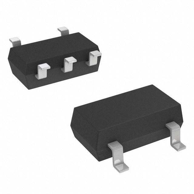
| 供应商器件封装 | 8-SOIC |
| 共模抑制比—最小值 | 58 dB |
| 关闭 | No Shutdown |
| 其它名称 | 296-12226-1 |
| 包装 | 剪切带 (CT) |
| 单位重量 | 72.600 mg |
| 压摆率 | 0.06 V/µs |
| 双重电源电压 | +/- 3 V, +/- 5 V |
| 商标 | Texas Instruments |
| 增益带宽生成 | 0.16 MHz |
| 增益带宽积 | 160kHz |
| 安装类型 | 表面贴装 |
| 安装风格 | SMD/SMT |
| 封装 | Reel |
| 封装/外壳 | 8-SOIC(0.154",3.90mm 宽) |
| 封装/箱体 | SOIC-8 |
| 工作温度 | -40°C ~ 125°C |
| 工作电源电压 | 2.7 V to 16 V, +/- 1.35 V to +/- 8 V |
| 工厂包装数量 | 2500 |
| 技术 | BiCMOS |
| 放大器类型 | 通用 |
| 最大双重电源电压 | +/- 8 V |
| 最大工作温度 | + 125 C |
| 最小双重电源电压 | +/- 1.35 V |
| 最小工作温度 | - 40 C |
| 标准包装 | 1 |
| 电压-电源,单/双 (±) | 2.7 V ~ 16 V, ±1.35 V ~ 8 V |
| 电压-输入失调 | 500µV |
| 电流-电源 | 7µA |
| 电流-输入偏置 | 1pA |
| 电流-输出/通道 | 400µA |
| 电源电流 | 0.02 mA |
| 电路数 | 2 |
| 系列 | TLV2382 |
| 转换速度 | 0.06 V/us |
| 输入偏压电流—最大 | 60 pA |
| 输入参考电压噪声 | 90 nV |
| 输入补偿电压 | 4.5 mV |
| 输出电流 | 0.4 mA |
| 输出类型 | 满摆幅 |
| 通道数量 | 2 Channel |


- 商务部:美国ITC正式对集成电路等产品启动337调查
- 曝三星4nm工艺存在良率问题 高通将骁龙8 Gen1或转产台积电
- 太阳诱电将投资9.5亿元在常州建新厂生产MLCC 预计2023年完工
- 英特尔发布欧洲新工厂建设计划 深化IDM 2.0 战略
- 台积电先进制程称霸业界 有大客户加持明年业绩稳了
- 达到5530亿美元!SIA预计今年全球半导体销售额将创下新高
- 英特尔拟将自动驾驶子公司Mobileye上市 估值或超500亿美元
- 三星加码芯片和SET,合并消费电子和移动部门,撤换高东真等 CEO
- 三星电子宣布重大人事变动 还合并消费电子和移动部门
- 海关总署:前11个月进口集成电路产品价值2.52万亿元 增长14.8%


PDF Datasheet 数据手册内容提取
TLV2381 TLV2382 SLOS377A – SEPTEMBER 2001– REVISED JULY 2003 FAMILY OF MICROPOWER RAIL-TO-RAIL INPUT AND OUTPUT OPERATIONAL AMPLIFIERS FEATURES DESCRIPTION (cid:0) BiMOS Rail-to-Rail Input/Output The TLV238x single supply operational amplifiers (cid:0) Input Bias Current...1 pA provide rail-to-rail input and output capability. The (cid:0) High Wide Bandwidth...160 kHz TLV238x takes the minimum operating supply voltage (cid:0) down to 2.7 V over the extended industrial temperature High Slew Rate...0.1 V/µs range, while adding the rail-to-rail output swing feature. (cid:0) Supply Current...7 µA (per channel) The TLV238x also provides 160-kHz bandwidth from (cid:0) Input Noise Voltage...90 nV/√Hz only 7 µA. The maximum recommended supply voltage (cid:0) Supply Voltage Range...2.7 V to 16 V is 16 V, which allows the devices to be operated from (cid:0) (±8V supplies down to ±1.35 V) two rechargeable cells. Specified Temperature Range – –40°C to 125°C...Industrial Grade The combination of rail-to-rail inputs and outputs make (cid:0) Ultra-Small Packaging them good upgrades for the TLC27Lx family—offering – 5 Pin SOT-23 (TLV2381) more bandwidth at a lower quiescent current. The offset voltage is lower than the TLC27LxA variant. APPLICATIONS To maintain cost effectiveness the TLV2381/2 are only (cid:0) available in the extended industrial temperature range. Portable Medical (cid:0) This means that one device can be used in a wide range Power Monitoring of applications that include PDAs as well as automotive (cid:0) Low Power Security Detection Systems sensor interface. (cid:0) Smoke Detectors All members are available in SOIC, with the singles in the small SOT-23 package, duals in the MSOP. SELECTION GUIDE VS IQ/ch VICR VIO IIB GBW SLEW RATE Vn, 1 kHz DEVICE [V] [µA] [V] [mV] [pA] [MHz] [V/µs] [nV/√Hz] TLV238x 2.7 to 16 10 –0.2 to VS + 0.2 4.5 60 0.16 0.06 100 TLV27Lx 2.7 to 16 11 –0.2 to VS – 1.2 5 60 0.16 0.06 100 TLC27Lx 4 to 16 17 –0.2 to VS – 1.5 10/5/2 60 0.085 0.03 68 OPAx349 1.8 to 5.5 2 –0.2 to VS + 0.2 10 10 0.070 0.02 300 OPAx347 2.3 to 5.5 34 –0.2 to VS + 0.2 6 10 0.35 0.01 60 TLC225x 2.7 to 16 62.5 0 to VS – 1.5 1.5/0.85 60 0.200 0.02 19 NOTE: All dc specs are maximums while ac specs are typicals. Please be aware that an important notice concerning availability, standard warranty, and use in critical applications of TexasInstruments semiconductor products and disclaimers thereto appears at the end of this data sheet. PRODUCTION DATA information is current as of publication date. Copyright 2001–2003 Texas Instruments Incorporated Products conform to specifications per the terms of Texas Instruments standard warranty. Production processing does not necessarily include testing of all parameters. www.ti.com 1
TLV2381 TLV2382 SLOS377A – SEPTEMBER 2001– REVISED JULY 2003 PACKAGE/ORDERING INFORMATION SPECIFIED PACKAGE PRODUCT PACKAGE SYMBOL TEMPERATURE ORDER NUMBER TRANSPORT MEDIA CODE RANGE TLV2381ID Tube TTLLVV22338811IIDD SSOOIICC--88 DD 22338811II TLV2381IDR Tape and Reel TLV2381IDBVR TTLLVV22338811IIDDBBVV SSOOTT--2233 DDBBVV VVBBKKII ––––44440000°°CCCC ttttoooo 111122225555°°CCCC TTaappee aanndd RReeeell TLV2381IDBVT TLV2382ID Tube TTLLVV22338822IIDD SSOOIICC--88 DD 22338822II TLV2382IDR Tape and Reel absolute maximum ratings over operating free-air temperature (unless otherwise noted)† Supply voltage, V . . . . . . . . . . . . . . . . . . . . . . . . . . . . . . . . . . . . . . . . . . . . . . . . . . . . . . . . . . . . . . . . . . . . . . . . . . . . 16.5 V S Input voltage, VI (see Notes 1 and 2) . . . . . . . . . . . . . . . . . . . . . . . . . . . . . . . . . . . . . . . . . . . . . . . . . . . . . . . . VS + 0.2 V Output current, I . . . . . . . . . . . . . . . . . . . . . . . . . . . . . . . . . . . . . . . . . . . . . . . . . . . . . . . . . . . . . . . . . . . . . . . . . . . . 100 mA O Differential input voltage, V . . . . . . . . . . . . . . . . . . . . . . . . . . . . . . . . . . . . . . . . . . . . . . . . . . . . . . . . . . . . . . . . . . . . . . V ID S Continuous total power dissipation . . . . . . . . . . . . . . . . . . . . . . . . . . . . . . . . . . . . . . . . . . See Dissipation Rating Table Maximum junction temperature, T . . . . . . . . . . . . . . . . . . . . . . . . . . . . . . . . . . . . . . . . . . . . . . . . . . . . . . . . . . . . . . 150°C J Operating free-air temperature range, T : I suffix . . . . . . . . . . . . . . . . . . . . . . . . . . . . . . . . . . . . . . . . . –40°C to 125°C A Storage temperature range, T . . . . . . . . . . . . . . . . . . . . . . . . . . . . . . . . . . . . . . . . . . . . . . . . . . . . . . . –65°C to 125°C stg Lead temperature 1,6 mm (1/16 inch) from case for 10 seconds . . . . . . . . . . . . . . . . . . . . . . . . . . . . . . . . . . . . . 300°C †Stresses beyond those listed under “absolute maximum ratings” may cause permanent damage to the device. These are stress ratings only, and functional operation of the device at these or any other conditions beyond those indicated under “recommended operating conditions” is not implied. Exposure to absolute-maximum-rated conditions for extended periods may affect device reliability. NOTES: 1. Relative to GND pin. 2. Maximum is 16.5 V or VS+0.2 V whichever is the lesser value. DISSIPATION RATING TABLE PACKAGE θJC θJA TA ≤ 25°C TA = 85°C (°C/W) (°C/W) POWER RATING POWER RATING D (8) 38.3 176 710 mW 370 mW DBV (5) 55 324.1 385 mW 201 mW DBV (6) 55 294.3 425 mW 221 mW 2 www.ti.com
TLV2381 TLV2382 SLOS377A – SEPTEMBER 2001– REVISED JULY 2003 recommended operating conditions MIN MAX UNIT Dual supply ±1.35 ±8 SSuuppppllyy vvoollttaaggee,, ((VVSS)) VV Single supply 2.7 16 Input common-mode voltage range –0.2 VS+0.2 V Operating free air temperature, TA I-suffix –40 125 °C electrical characteristics at recommended operating conditions, V = 2.7 V, 5 V, and 15 V (unless S otherwise noted) dc performance PARAMETER TEST CONDITIONS TA† MIN TYP MAX UNIT 25°C 0.5 4.5 VVIIOO IInnppuutt ooffffsseett vvoollttaaggee VVIICC == VVSS//22,, VVOO == VVSS//22 Full range 6.5 mmVV RRLL == 110000 kkΩΩ RRSS == 5500 ΩΩ αVIO Offset voltage drift 25°C 1.1 µV/°C VVIICC == 00 VV ttoo VVSS,, 25°C 54 69 RS = 50 Ω Full range 53 VVVSS === 222...777 VVV dddBBB VVIICC == 00 VV ttoo VVSS––11..33 VV,, 25°C 71 86 RS = 50 Ω Full range 70 VVIICC == 00 VV ttoo VVSS,, 25°C 58 74 RS = 50 Ω Full range 57 CCCCCCCMMMMMMMRRRRRRRRRRRRRR CCCCCCCooooooommmmmmmmmmmmmmooooooonnnnnnn-------mmmmmmmooooooodddddddeeeeeee rrrrrrreeeeeeejjjjjjjeeeeeeeccccccctttttttiiiiiiiooooooonnnnnnn rrrrrrraaaaaaatttttttiiiiiiiooooooo VVVSS === 555 VVV dddBBB VVIICC == 00 VV ttoo VVSS––11..33 VV,, 25°C 72 88 RS = 50 Ω Full range 70 VVIICC == 00 VV ttoo VVSS,, 25°C 65 80 RS = 50 Ω Full range 64 VVVSS === 111555 VVV dddBBB VVIICC == 00 VV ttoo VVSS––11..33 VV,, 25°C 72 90 RS = 50 Ω Full range 70 25°C 80 100 VVSS == 22..77 VV Full range 77 AAAAVVDD LLLLaaaaamrrrrpggggleeeeif----icssssaiiiiggggtnnnnioaaaanllll ddddiiiiffffffffeeeerrrreeeennnnttttiiiiaaaallll vvvvoooollllttttaaaaggggeeee VVVVROOL ((=PP 1PP0))0==== kVVVVΩSS////2222,,,, VVSS == 55 VV Fu2ll 5ra°Cnge 8707 100 ddddBBBB 25°C 77 83 VVSS == 1155 VV Full range 74 †Full range is –40°C to 125°C. input characteristics PARAMETER TEST CONDITIONS TA MIN TYP MAX UNIT ≤25°C 1 60 IIIIOO IInnppuutt ooffffsseett ccuurrrreenntt ≤70°C 100 ppAA VVVVIICC ==== VVVVSS////2222,,,, VVVVOO ==== VVVVSS////2222,,,, ≤125°C 1000 RL = 100 kΩ , RS = 50 Ω ≤25°C 1 60 IIIIBB IInnppuutt bbiiaass ccuurrrreenntt ≤70°C 200 ppAA ≤125°C 1000 ri(d) Differential input resistance 25°C 1000 GΩ CIC Common-mode input capacitance f = 1 kHz 25°C 8 pF www.ti.com 3
TLV2381 TLV2382 SLOS377A – SEPTEMBER 2001– REVISED JULY 2003 electrical characteristics at recommended operating conditions, V = 2.7 V, 5 V, and 15 V (unless S otherwise noted) (continued) power supply PARAMETER TEST CONDITIONS TA† MIN TYP MAX UNIT 25°C 7 10 IIDDDD SSuuppppllyy ccuurrrreenntt ((ppeerr cchhaannnneell)) VVOO == VVSS//22 µµAA Full range 15 PPSSRRRR PPoowweerr ssuuppppllyy rreejjeeccttiioonn rraattiioo ((∆∆VVSS//∆∆VVIIOO)) VVSS == 22..77 VV ttoo 1166VV,, NNoo llooaadd,, 25°C 74 82 ddBB VIC = VS/2 V Full range 70 †Full range is –40°C to 125°C for I suffix. output characteristics PARAMETER TEST CONDITIONS TA† MIN TYP MAX UNIT 25°C 200 160 VVSS == 22..77 VV Full range 220 VVVVIOIICC = ====1 0VVVV0SS µ////2222A,,,, VVSS == 55 VV Fu2ll 5ra°Cnge 122000 85 mmmmVVVV 25°C 120 50 VVVVVVOO OOOOOOuuuuuuttttttppppppuuuuuutttttt vvvvvvoooooollllllttttttaaaaaaggggggeeeeee sssssswwwwwwiiiiiinnnnnngggggg ffffffrrrrrroooooommmmmm rrrrrraaaaaaiiiiiillllll VVSS == 1155 VV Full range 150 25°C 800 420 VVSS == 55 VV VVVIICC === VVVSS///222,,, Full range 900 mmmVVV IO = 500 µA 25°C 400 200 VVSS == 1155 VV Full range 500 IO Output current VO = 0.5 V from rail VS = 2.7 V 25°C 400 µA †Full range is –40°C to 125°C for I suffix. dynamic performance PARAMETER TEST CONDITIONS TA MIN TYP MAX UNIT GBP Gain bandwidth product RL = 100 kΩ , CL = 10 pF, f = 1 kHz 25°C 160 kHz 25°C 0.06 SSRR SSlleeww rraattee aatt uunniittyy ggaaiinn VVOO((pppp)) == 22 VV,, RRLL == 110000 kkΩΩ, –40°C 0.05 VV//µss CCLL == 1100 ppFF 125°C 0.08 φM Phase margin 25°C 62 ° RRLL == 110000 kkΩΩ,, CCLL == 5500 ppFF Gain margin 25°C 6.7 dB ttss SSeettttlliinngg ttiimmee ((00..11%%)) VVC((LSS =TT EE1PP0 ))pppFpp, == 11 VV ,, R AALVV = == 1 0––011 ,,kΩ RFaislle 2255°°CC 3611 µµss noise/distortion performance PARAMETER TEST CONDITIONS TA MIN TYP MAX UNIT Vn Equivalent input noise voltage f = 1 kHz 25°C 90 nV/√Hz 4 www.ti.com
TLV2381 TLV2382 SLOS377A – SEPTEMBER 2001– REVISED JULY 2003 TYPICAL CHARACTERISTICS Table of Graphs FIGURE VIO Input offset voltage vs Common-mode input voltage 1, 2, 3 IIB/IIO Input bias and offset current vs Free-air temperature 4 VOH High-level output voltage vs High-level output current 5, 7, 9 VOL Low-level output voltage vs Low-level output current 6, 8, 10 vs Supply voltage 11 IIQQ QQuuiieesscceenntt ccuurrrreenntt vs Free-air temperature 12 Supply voltage and supply current ramp up 13 AVD Differential voltage gain and phase shift vs Frequency 14 GBP Gain-bandwidth product vs Free-air temperature 15 φm Phase margin vs Load capacitance 16 CMRR Common-mode rejection ratio vs Frequency 17 PSRR Power supply rejection ratio vs Frequency 18 Input referred noise voltage vs Frequency 19 SR Slew rate vs Free-air temperature 20 VO(PP) Peak-to-peak output voltage vs Frequency 21 Inverting small-signal response 22 Inverting large-signal response 23 Crosstalk vs Frequency 24 INPUT OFFSET VOLTAGE INPUT OFFSET VOLTAGE INPUT OFFSET VOLTAGE vs vs vs COMMON-MODE INPUT VOLTAGE COMMON-MODE INPUT VOLTAGE COMMON-MODE INPUT VOLTAGE 2000 2000 2000 µV– Input Offset Voltage – AIO––1111–5005550000000000000 VTAS == 225.7°C V µV– Input Offset Voltage – AIO––11–115050550000000000000 VTAS == 255 V°C µV– Input Offset Voltage – AIO––1111–5005550000000000000 VTAS == 2155° CV –2000 –2000 –2000 0 0.3 0.6 0.9 1.2 1.5 1.8 2.1 2.4 2.7 0 0.5 1 1.5 2 2.5 3 3.5 4 4.5 5 –0.2 7.5 15.2 VIC – Common-Mode Input Voltage – V VIC – Common-Mode Input Voltage – V VIC – Common-Mode Input Voltage – V Figure 1 Figure 2 Figure 3 www.ti.com 5
TLV2381 TLV2382 SLOS377A – SEPTEMBER 2001– REVISED JULY 2003 TYPICAL CHARACTERISTICS INPUT BIAS AND INPUT OFFSET CURRENT HIGH-LEVEL OUTPUT VOLTAGE LOW-LEVEL OUTPUT VOLTAGE vs vs vs FREE-AIR TEMPERATURE HIGH-LEVEL OUTPUT CURRENT LOW-LEVEL OUTPUT CURRENT 100 15 15 – Input Bias and Input IIandIBIOOffset Currents – pA 4329876500000000 VVVRDIOSCD ===± 50 0=0 ±Ω2.5 V IIB IIO – High-Level Output Voltage – VH12271...05555 1–2450°C°C 0°CV2S5 °=C 7105° VC – Low-Level Output Voltage – VL 111110234234567891 VS = 15 0V°2C57°01C°2C5°C –40°C 10 VO VO 1 025 45 65 85 105 125 00 2 4 6 8 10 12 14 16 18 20 22 24 00 2 4 6 8 10 12 14 16 18 20 TA – Free-Air Temperature – °C IOH – High-Level Output Current – mA IOL – Low-Level Output Current – mA Figure 4 Figure 5 Figure 6 HIGH-LEVEL OUTPUT VOLTAGE LOW-LEVEL OUTPUT VOLTAGE HIGH-LEVEL OUTPUT VOLTAGE vs vs vs HIGH-LEVEL OUTPUT CURRENT LOW-LEVEL OUTPUT CURRENT HIGH-LEVEL OUTPUT CURRENT 5 5 2.7 VS = 5 V VS = 5 V VS = 2.7 V V 4.5 4.5 V 2.4 – –40°C V 125°C – –40°C h-Level Output Voltage 123...234555 0°C25°C70°C Level Output Voltage – 123...234555 02°C57°0C°C h-Level Output Voltage 01112.....92581 0°C25°C70°C – HigVOH 0.15 125°C – Low-VOL 0.15 –40°C – HigVOH 00..36 125°C 0 0 0 0 0.5 1 1.5 2 2.5 3 3.5 4 4.5 5 0 0.5 1 1.5 2 2.5 3 3.5 4 4.5 55.5 6 0 0.2 0.4 0.6 0.8 1 1.2 1.4 IOH – High-Level Output Current – mA IOL – Low-Level Output Current – mA IOH – High-Level Output Current – mA Figure 7 Figure 8 Figure 9 QUIESCENT CURRENT LOW-LEVEL OUTPUT VOLTAGE QUIESCENT CURRENT vs vs vs FREE-AIR TEMPERATURE LOW-LEVEL OUTPUT CURRENT SUPPLY VOLTAGE 8 2.7 8 16 V VS = 2.7 V 125°C 7 ge – V 22..14 7102°5C°C µnr – A 67 70°C µnr – A 6 5 V el Output Volta 111...258 02°C5°C uiescent Curre 345 –40°C 0°C 25°C uiescent Curre 345 2.7 V Lev 0.9 – Q – Q 2 – Low-L 00..36 –40°C I(Q) 12 I(Q) 1 O V 0 0 0 –40–25–10 5 20 35 50 65 80 95110125 0 0.2 0.4 0.6 0.8 1 1.2 1.4 0 2 4 6 8 10 12 14 16 IOL – Low-Level Output Current – mA VS – Supply Voltage – V TA – Free-Air Temperature – °C Figure 10 Figure 11 Figure 12 6 www.ti.com
TLV2381 TLV2382 SLOS377A – SEPTEMBER 2001– REVISED JULY 2003 TYPICAL CHARACTERISTICS DIFFERENTIAL VOLTAGE GAIN AND PHASE SHIFT SUPPLY VOLTAGE AND vs SUPPLY CURRENT RAMP UP FREQUENCY c 15 40 120 oltage – V/d 105 VS VO ain – dB 10800 VRCTASLL ==== 2115500 V°0 pC kFΩ 030°° V G V– Supply S 0 VRCTASLL ==== 2110500 t°0 opC ΩF1,5, V, 15 µurrent – A ential Voltage 4600 6900°° Phase Shift IQ 10 ply C Differ 20 120° 5 – Sup – VD 0 150° C A 0 IC –20 180° 0 5 10 15 20 25 30 0.1 1 10 100 1 k 10 k 100 k 1 M t – Time – ms f – Frequency – Hz Figure 13 Figure 14 GAIN-BANDWIDTH PRODUCT PHASE MARGIN COMMON-MODE REJECTION RATIO vs vs vs FREE-AIR TEMPERATURE LOAD CAPACITANCE FREQUENCY 170 80 B 120 GBP – Gain-Bandwidth Product – kHz 111111234561000000 VS = 2.7 V VS = 5 V VS = 15 V Phase Margin – Degrees 12345670000000 VRTASL === 21550 V°0C kΩ R – Common-Mode Rejection Ratio – d 110123456789100000000000 VTAS == 255 V°C 100 0 MR 0 –40–25–105 20 35 50 65 80 95 110125 10 100 1000 C 10 100 1 k 10 k 100 k 1 M TA – Free-Air Temperature – °C CL – Load Capacitance – pF f – Frequency – Hz Figure 15 Figure 16 Figure 17 POWER SUPPLY REJECTION RATIO INPUT REFERRED NOISE VOLTAGE SLEW RATE vs vs vs FREQUENCY FREQUENCY FREE-AIR TEMPERATURE B 100 Hz 250 0.09 wer Supply Rejection Ratio – d 34567890000000 VTAS == ±225.°5C V Referred Noise Voltage –nV/ 112050000 VGRSF = == 2 ,51 0V0, kΩ µsSR – Slew Rate – V/ 000000......000000345678 SR+ SRVG–Sai n= =5 1V Po 20 ut 50 0.02 VO = 1 PSRR – 100 – InpVn 0 0.001 RCLL == 15000 p kFΩ 10 100 1 k 10 k 100 k 1 M 1 10 100 1 k 10 k 100 k –40–25–10 5 20 35 50 65 80 95 110125 f – Frequency – Hz f – Frequency – Hz TA – Free-air Temperature –°C Figure 18 Figure 19 Figure 20 www.ti.com 7
TLV2381 TLV2382 SLOS377A – SEPTEMBER 2001– REVISED JULY 2003 TYPICAL CHARACTERISTICS PEAK-TO-PEAK OUTPUT VOLTAGE INVERTING SMALL-SIGNAL vs RESPONSE FREQUENCY 16 2 k – V 14 VS = 15 V 1.5 VI = 3 VPP a e o-P 12 1 Gain = –1, e Peak-t 10 RCLL == 11000 p kF,Ω, e – VPP 0.5 RCVSLL === 11500 V0 p, kF,Ω, ut Voltag 68 THD+N <= 5% Amplitud –0.05 Vf =O 1 = k 3H VzPP, p Out 4 VS = 5 V –1 – OPP 2 VS = 2.7 V –1.5 VO = 3 VPP V 0 –2 10 100 1000 1 k 10 k –100 0 100 200 300 400 500 600 700 f – Frequency – Hz t – Time – µs Figure 21 Figure 22 CROSSTALK INVERTING LARGE-SIGNAL vs RESPONSE FREQUENCY 0.06 0 VS = 5 V –20 RL = 2 kΩ 0.04 VI = 100 mVPP CL = 10 pF TA = 25°C Gain = –1, –40 Channel 1 to 2 PP 0.02 RL = 100 kΩ, B plitude – V 0 CVVf =SOL 1 === k 151H0 0Vz 0p, Fm,VPP, osstalk – d ––8600 Am –0.02 Cr –100 –0.04 –120 VO = 100 mVPP –140 –0.06 –100 0 100 200 300 400 500 600 700 10 100 1 k 10 k 100 k t – Time – µs f – Frequency – Hz Figure 23 Figure 24 8 www.ti.com
TLV2381 TLV2382 SLOS377A – SEPTEMBER 2001– REVISED JULY 2003 APPLICATION INFORMATION offset voltage The output offset voltage (V ) is the sum of the input offset voltage (V ) and both input bias currents (I ) times the OO IO IB corresponding gains. The following schematic and formula can be used to calculate the output offset voltage: RF IIB– RG + – (cid:1) (cid:1)RF(cid:3)(cid:3) (cid:1) (cid:1)RF(cid:3)(cid:3) VI + VO VOO(cid:0)VIO 1(cid:2) R (cid:4)IIB(cid:2) RS 1(cid:2) R (cid:4)IIB– RF G G RS IIB+ Figure 25. Output Offset Voltage Model general configurations When receiving low-level signals, limiting the bandwidth of the incoming signals into the system is often required. The simplest way to accomplish this is to place an RC filter at the noninverting terminal of the amplifier (see Figure 26). RG RF VO (cid:0) (cid:1)1(cid:2)RF(cid:3)(cid:1) 1 (cid:3) VDD/2 VI RG 1(cid:2)sR1C1 – VI + VO f–3dB (cid:0) 2(cid:0)R11C1 R1 C1 Figure 26. Single-Pole Low-Pass Filter If even more attenuation is needed, a multiple pole filter is required. The Sallen-Key filter can be used for this task. For best results, the amplifier should have a bandwidth that is 8 to 10 times the filter frequency bandwidth. Failure to do this can result in phase shift of the amplifier. C1 R1 = R2 = R C1 = C2 = C Q = Peaking Factor (Butterworth Q = 0.707) VI + R1 R2 _ f–3dB (cid:0) 2(cid:0)1RC C2 RF RG = RF (2 – 1 ) RG Q VDD/2 Figure 27. 2-Pole Low-Pass Sallen-Key Filter www.ti.com 9
TLV2381 TLV2382 SLOS377A – SEPTEMBER 2001– REVISED JULY 2003 APPLICATION INFORMATION circuit layout considerations To achieve the levels of high performance of the TLV238x, follow proper printed-circuit board design techniques. A general set of guidelines is given in the following. (cid:0) Ground planes—It is highly recommended that a ground plane be used on the board to provide all components with a low inductive ground connection. However, in the areas of the amplifier inputs and output, the ground plane can be removed to minimize the stray capacitance. (cid:0) Proper power supply decoupling—Use a 6.8-µF tantalum capacitor in parallel with a 0.1-µF ceramic capacitor on each supply terminal. It may be possible to share the tantalum among several amplifiers depending on the application, but a 0.1-µF ceramic capacitor should always be used on the supply terminal of every amplifier. In addition, the 0.1-µF capacitor should be placed as close as possible to the supply terminal. As this distance increases, the inductance in the connecting trace makes the capacitor less effective. The designer should strive for distances of less than 0.1 inches between the device power terminals and the ceramic capacitors. (cid:0) Sockets—Sockets can be used but are not recommended. The additional lead inductance in the socket pins will often lead to stability problems. Surface-mount packages soldered directly to the printed-circuit board is the best implementation. (cid:0) Short trace runs/compact part placements—Optimum high performance is achieved when stray series inductance has been minimized. To realize this, the circuit layout should be made as compact as possible, thereby minimizing the length of all trace runs. Particular attention should be paid to the inverting input of the amplifier. Its length should be kept as short as possible. This will help to minimize stray capacitance at the input of the amplifier. (cid:0) Surface-mount passive components—Using surface-mount passive components is recommended for high performance amplifier circuits for several reasons. First, because of the extremely low lead inductance of surface-mount components, the problem with stray series inductance is greatly reduced. Second, the small size of surface-mount components naturally leads to a more compact layout thereby minimizing both stray inductance and capacitance. If leaded components are used, it is recommended that the lead lengths be kept as short as possible. 10 www.ti.com
TLV2381 TLV2382 SLOS377A – SEPTEMBER 2001– REVISED JULY 2003 APPLICATION INFORMATION general power dissipation considerations For a given θ , the maximum power dissipation is shown in Figure 28 and is calculated by the following formula: JA (cid:1)TMAX–TA(cid:2) PD(cid:0) (cid:0) JA Where: P = Maximum power dissipation of TLV238x IC (watts) D T = Absolute maximum junction temperature (150°C) MAX T = Free-ambient air temperature (°C) A θJA = θJC + θCA θJC = Thermal coefficient from junction to case θ = Thermal coefficient from case to ambient air (°C/W) CA MAXIMUM POWER DISSIPATION vs FREE-AIR TEMPERATURE 2 PDIP Package TJ = 150°C 1.75 Low-K Test PCB θJA = 104°C/W W n – 1.5 MSOP Package o pati 1.25 SOIC Package LθJoAw -=K 2 T6e0s°tC P/WCB si Low-K Test PCB Dis θJA = 176°C/W r 1 e w o P m 0.75 u m xi 0.5 a M 0.25 SOT-23 Package Low-K Test PCB 0 θJA = 324°C/W –55–40–25 –10 5 20 35 50 65 80 95 110 125 TA – Free-Air Temperature – °C NOTE A: Results are with no air flow and using JEDEC Standard Low-K test PCB. Figure 28. Maximum Power Dissipation vs Free-Air Temperature TLV2381 TLV2381 TLV2382 DBV PACKAGE D PACKAGE D PACKAGE (TOP VIEW) (TOP VIEW) (TOP VIEW) OUT 1 5 VDD NC 1 8 NC 1OUT 1 8 VDD IN– 2 7 VDD 1IN– 2 7 2OUT GND 2 IN+ 3 6 OUT 1IN+ 3 6 2IN– GND 4 5 NC GND 4 5 2IN+ IN+ 3 4 IN– NC – No internal connection www.ti.com 11
PACKAGE OPTION ADDENDUM www.ti.com 6-Feb-2020 PACKAGING INFORMATION Orderable Device Status Package Type Package Pins Package Eco Plan Lead/Ball Finish MSL Peak Temp Op Temp (°C) Device Marking Samples (1) Drawing Qty (2) (6) (3) (4/5) TLV2381ID ACTIVE SOIC D 8 75 Green (RoHS NIPDAU Level-1-260C-UNLIM -40 to 125 2381I & no Sb/Br) TLV2381IDBVR ACTIVE SOT-23 DBV 5 3000 Green (RoHS NIPDAU Level-1-260C-UNLIM -40 to 125 VBKI & no Sb/Br) TLV2381IDBVRG4 ACTIVE SOT-23 DBV 5 3000 Green (RoHS NIPDAU Level-1-260C-UNLIM -40 to 125 VBKI & no Sb/Br) TLV2381IDBVT ACTIVE SOT-23 DBV 5 250 Green (RoHS NIPDAU Level-1-260C-UNLIM -40 to 125 VBKI & no Sb/Br) TLV2381IDR ACTIVE SOIC D 8 2500 Green (RoHS NIPDAU Level-1-260C-UNLIM -40 to 125 2381I & no Sb/Br) TLV2382ID ACTIVE SOIC D 8 75 Green (RoHS NIPDAU Level-1-260C-UNLIM -40 to 125 2382I & no Sb/Br) TLV2382IDG4 ACTIVE SOIC D 8 75 Green (RoHS NIPDAU Level-1-260C-UNLIM -40 to 125 2382I & no Sb/Br) TLV2382IDR ACTIVE SOIC D 8 2500 Green (RoHS NIPDAU Level-1-260C-UNLIM -40 to 125 2382I & no Sb/Br) (1) The marketing status values are defined as follows: ACTIVE: Product device recommended for new designs. LIFEBUY: TI has announced that the device will be discontinued, and a lifetime-buy period is in effect. NRND: Not recommended for new designs. Device is in production to support existing customers, but TI does not recommend using this part in a new design. PREVIEW: Device has been announced but is not in production. Samples may or may not be available. OBSOLETE: TI has discontinued the production of the device. (2) RoHS: TI defines "RoHS" to mean semiconductor products that are compliant with the current EU RoHS requirements for all 10 RoHS substances, including the requirement that RoHS substance do not exceed 0.1% by weight in homogeneous materials. Where designed to be soldered at high temperatures, "RoHS" products are suitable for use in specified lead-free processes. TI may reference these types of products as "Pb-Free". RoHS Exempt: TI defines "RoHS Exempt" to mean products that contain lead but are compliant with EU RoHS pursuant to a specific EU RoHS exemption. Green: TI defines "Green" to mean the content of Chlorine (Cl) and Bromine (Br) based flame retardants meet JS709B low halogen requirements of <=1000ppm threshold. Antimony trioxide based flame retardants must also meet the <=1000ppm threshold requirement. (3) MSL, Peak Temp. - The Moisture Sensitivity Level rating according to the JEDEC industry standard classifications, and peak solder temperature. (4) There may be additional marking, which relates to the logo, the lot trace code information, or the environmental category on the device. Addendum-Page 1
PACKAGE OPTION ADDENDUM www.ti.com 6-Feb-2020 (5) Multiple Device Markings will be inside parentheses. Only one Device Marking contained in parentheses and separated by a "~" will appear on a device. If a line is indented then it is a continuation of the previous line and the two combined represent the entire Device Marking for that device. (6) Lead/Ball Finish - Orderable Devices may have multiple material finish options. Finish options are separated by a vertical ruled line. Lead/Ball Finish values may wrap to two lines if the finish value exceeds the maximum column width. Important Information and Disclaimer:The information provided on this page represents TI's knowledge and belief as of the date that it is provided. TI bases its knowledge and belief on information provided by third parties, and makes no representation or warranty as to the accuracy of such information. Efforts are underway to better integrate information from third parties. TI has taken and continues to take reasonable steps to provide representative and accurate information but may not have conducted destructive testing or chemical analysis on incoming materials and chemicals. TI and TI suppliers consider certain information to be proprietary, and thus CAS numbers and other limited information may not be available for release. In no event shall TI's liability arising out of such information exceed the total purchase price of the TI part(s) at issue in this document sold by TI to Customer on an annual basis. Addendum-Page 2
PACKAGE MATERIALS INFORMATION www.ti.com 19-Mar-2008 TAPE AND REEL INFORMATION *Alldimensionsarenominal Device Package Package Pins SPQ Reel Reel A0(mm) B0(mm) K0(mm) P1 W Pin1 Type Drawing Diameter Width (mm) (mm) Quadrant (mm) W1(mm) TLV2381IDBVR SOT-23 DBV 5 3000 180.0 9.0 3.15 3.2 1.4 4.0 8.0 Q3 TLV2381IDBVT SOT-23 DBV 5 250 180.0 9.0 3.15 3.2 1.4 4.0 8.0 Q3 TLV2381IDR SOIC D 8 2500 330.0 12.4 6.4 5.2 2.1 8.0 12.0 Q1 TLV2382IDR SOIC D 8 2500 330.0 12.4 6.4 5.2 2.1 8.0 12.0 Q1 PackMaterials-Page1
PACKAGE MATERIALS INFORMATION www.ti.com 19-Mar-2008 *Alldimensionsarenominal Device PackageType PackageDrawing Pins SPQ Length(mm) Width(mm) Height(mm) TLV2381IDBVR SOT-23 DBV 5 3000 182.0 182.0 20.0 TLV2381IDBVT SOT-23 DBV 5 250 182.0 182.0 20.0 TLV2381IDR SOIC D 8 2500 340.5 338.1 20.6 TLV2382IDR SOIC D 8 2500 340.5 338.1 20.6 PackMaterials-Page2
PACKAGE OUTLINE DBV0005A SOT-23 - 1.45 mm max height SCALE 4.000 SMALL OUTLINE TRANSISTOR C 3.0 2.6 0.1 C 1.75 1.45 1.45 B A 0.90 PIN 1 INDEX AREA 1 5 2X 0.95 3.05 2.75 1.9 1.9 2 4 3 0.5 5X 0.3 0.15 0.2 C A B (1.1) TYP 0.00 0.25 GAGE PLANE 0.22 TYP 0.08 8 TYP 0.6 0 0.3 TYP SEATING PLANE 4214839/E 09/2019 NOTES: 1. All linear dimensions are in millimeters. Any dimensions in parenthesis are for reference only. Dimensioning and tolerancing per ASME Y14.5M. 2. This drawing is subject to change without notice. 3. Refernce JEDEC MO-178. 4. Body dimensions do not include mold flash, protrusions, or gate burrs. Mold flash, protrusions, or gate burrs shall not exceed 0.15 mm per side. www.ti.com
EXAMPLE BOARD LAYOUT DBV0005A SOT-23 - 1.45 mm max height SMALL OUTLINE TRANSISTOR PKG 5X (1.1) 1 5 5X (0.6) SYMM (1.9) 2 2X (0.95) 3 4 (R0.05) TYP (2.6) LAND PATTERN EXAMPLE EXPOSED METAL SHOWN SCALE:15X SOLDER MASK SOLDER MASK METAL UNDER METAL OPENING OPENING SOLDER MASK EXPOSED METAL EXPOSED METAL 0.07 MAX 0.07 MIN ARROUND ARROUND NON SOLDER MASK SOLDER MASK DEFINED DEFINED (PREFERRED) SOLDER MASK DETAILS 4214839/E 09/2019 NOTES: (continued) 5. Publication IPC-7351 may have alternate designs. 6. Solder mask tolerances between and around signal pads can vary based on board fabrication site. www.ti.com
EXAMPLE STENCIL DESIGN DBV0005A SOT-23 - 1.45 mm max height SMALL OUTLINE TRANSISTOR PKG 5X (1.1) 1 5 5X (0.6) SYMM 2 (1.9) 2X(0.95) 3 4 (R0.05) TYP (2.6) SOLDER PASTE EXAMPLE BASED ON 0.125 mm THICK STENCIL SCALE:15X 4214839/E 09/2019 NOTES: (continued) 7. Laser cutting apertures with trapezoidal walls and rounded corners may offer better paste release. IPC-7525 may have alternate design recommendations. 8. Board assembly site may have different recommendations for stencil design. www.ti.com
PACKAGE OUTLINE D0008A SOIC - 1.75 mm max height SCALE 2.800 SMALL OUTLINE INTEGRATED CIRCUIT C SEATING PLANE .228-.244 TYP [5.80-6.19] .004 [0.1] C A PIN 1 ID AREA 6X .050 [1.27] 8 1 2X .189-.197 [4.81-5.00] .150 NOTE 3 [3.81] 4X (0 -15 ) 4 5 8X .012-.020 B .150-.157 [0.31-0.51] .069 MAX [3.81-3.98] .010 [0.25] C A B [1.75] NOTE 4 .005-.010 TYP [0.13-0.25] 4X (0 -15 ) SEE DETAIL A .010 [0.25] .004-.010 0 - 8 [0.11-0.25] .016-.050 [0.41-1.27] DETAIL A (.041) TYPICAL [1.04] 4214825/C 02/2019 NOTES: 1. Linear dimensions are in inches [millimeters]. Dimensions in parenthesis are for reference only. Controlling dimensions are in inches. Dimensioning and tolerancing per ASME Y14.5M. 2. This drawing is subject to change without notice. 3. This dimension does not include mold flash, protrusions, or gate burrs. Mold flash, protrusions, or gate burrs shall not exceed .006 [0.15] per side. 4. This dimension does not include interlead flash. 5. Reference JEDEC registration MS-012, variation AA. www.ti.com
EXAMPLE BOARD LAYOUT D0008A SOIC - 1.75 mm max height SMALL OUTLINE INTEGRATED CIRCUIT 8X (.061 ) [1.55] SYMM SEE DETAILS 1 8 8X (.024) [0.6] SYMM (R.002 ) TYP [0.05] 5 4 6X (.050 ) [1.27] (.213) [5.4] LAND PATTERN EXAMPLE EXPOSED METAL SHOWN SCALE:8X SOLDER MASK SOLDER MASK METAL OPENING OPENING METAL UNDER SOLDER MASK EXPOSED METAL EXPOSED METAL .0028 MAX .0028 MIN [0.07] [0.07] ALL AROUND ALL AROUND NON SOLDER MASK SOLDER MASK DEFINED DEFINED SOLDER MASK DETAILS 4214825/C 02/2019 NOTES: (continued) 6. Publication IPC-7351 may have alternate designs. 7. Solder mask tolerances between and around signal pads can vary based on board fabrication site. www.ti.com
EXAMPLE STENCIL DESIGN D0008A SOIC - 1.75 mm max height SMALL OUTLINE INTEGRATED CIRCUIT 8X (.061 ) [1.55] SYMM 1 8 8X (.024) [0.6] SYMM (R.002 ) TYP [0.05] 5 4 6X (.050 ) [1.27] (.213) [5.4] SOLDER PASTE EXAMPLE BASED ON .005 INCH [0.125 MM] THICK STENCIL SCALE:8X 4214825/C 02/2019 NOTES: (continued) 8. Laser cutting apertures with trapezoidal walls and rounded corners may offer better paste release. IPC-7525 may have alternate design recommendations. 9. Board assembly site may have different recommendations for stencil design. www.ti.com
IMPORTANTNOTICEANDDISCLAIMER TI PROVIDES TECHNICAL AND RELIABILITY DATA (INCLUDING DATASHEETS), DESIGN RESOURCES (INCLUDING REFERENCE DESIGNS), APPLICATION OR OTHER DESIGN ADVICE, WEB TOOLS, SAFETY INFORMATION, AND OTHER RESOURCES “AS IS” AND WITH ALL FAULTS, AND DISCLAIMS ALL WARRANTIES, EXPRESS AND IMPLIED, INCLUDING WITHOUT LIMITATION ANY IMPLIED WARRANTIES OF MERCHANTABILITY, FITNESS FOR A PARTICULAR PURPOSE OR NON-INFRINGEMENT OF THIRD PARTY INTELLECTUAL PROPERTY RIGHTS. These resources are intended for skilled developers designing with TI products. You are solely responsible for (1) selecting the appropriate TI products for your application, (2) designing, validating and testing your application, and (3) ensuring your application meets applicable standards, and any other safety, security, or other requirements. These resources are subject to change without notice. TI grants you permission to use these resources only for development of an application that uses the TI products described in the resource. Other reproduction and display of these resources is prohibited. No license is granted to any other TI intellectual property right or to any third party intellectual property right. TI disclaims responsibility for, and you will fully indemnify TI and its representatives against, any claims, damages, costs, losses, and liabilities arising out of your use of these resources. TI’s products are provided subject to TI’s Terms of Sale (www.ti.com/legal/termsofsale.html) or other applicable terms available either on ti.com or provided in conjunction with such TI products. TI’s provision of these resources does not expand or otherwise alter TI’s applicable warranties or warranty disclaimers for TI products. Mailing Address: Texas Instruments, Post Office Box 655303, Dallas, Texas 75265 Copyright © 2020, Texas Instruments Incorporated