ICGOO在线商城 > 集成电路(IC) > 线性 - 放大器 - 仪表,运算放大器,缓冲器放大器 > OP727ARZ
 Datasheet下载
- 型号: OP727ARZ
- 制造商: Analog
- 库位|库存: xxxx|xxxx
- 要求:
| 数量阶梯 | 香港交货 | 国内含税 |
| +xxxx | $xxxx | ¥xxxx |
查看当月历史价格
查看今年历史价格
OP727ARZ产品简介:
ICGOO电子元器件商城为您提供OP727ARZ由Analog设计生产,在icgoo商城现货销售,并且可以通过原厂、代理商等渠道进行代购。 OP727ARZ价格参考¥23.82-¥40.57。AnalogOP727ARZ封装/规格:线性 - 放大器 - 仪表,运算放大器,缓冲器放大器, 通用 放大器 2 电路 满摆幅 8-SOIC。您可以下载OP727ARZ参考资料、Datasheet数据手册功能说明书,资料中有OP727ARZ 详细功能的应用电路图电压和使用方法及教程。
Analog Devices Inc.的OP727ARZ是一款高精度、低功耗的运算放大器,适用于多种精密测量和信号处理应用场景。以下是其主要应用领域:

 1. 精密测量仪器
OP727ARZ具有极低的输入偏置电流(典型值为1 pA),这使得它非常适合用于高阻抗传感器的信号调理电路中,如pH电极、光电二极管等。在这些应用中,微弱的信号需要被精确放大而不会引入显著的噪声或误差。

 2. 医疗设备
在医疗设备中,如心电图(ECG)、脑电图(EEG)和其他生物电位测量设备,OP727ARZ可以作为前置放大器,确保对微弱生物电信号的高精度放大。其低噪声和低漂移特性有助于提高测量的准确性,同时其低功耗设计适合便携式医疗设备。

 3. 工业自动化与控制系统
在工业环境中,OP727ARZ可用于压力传感器、温度传感器等传感器接口电路中,将传感器输出的微小信号放大到适合后续处理的水平。其出色的稳定性和低温漂特性使其能够在恶劣的工业环境中保持高精度。

 4. 音频处理
对于高端音频设备,如麦克风前置放大器或高保真音响系统,OP727ARZ能够提供非常低的失真和噪声性能,确保音频信号的纯净度和保真度。

 5. 数据采集系统
在数据采集系统中,OP727ARZ可以用作缓冲器或增益级,以确保信号在传输过程中不失真,并且能够适应不同的负载条件。其低功耗特性也使得它适合长时间运行的数据采集任务。

 6. 科学实验与研究
在实验室环境中,OP727ARZ常用于各种科学研究中,如物理实验、化学分析等,特别是在需要高精度信号放大的场合。其卓越的线性度和稳定性使得它成为科学家们信赖的选择。

总之,OP727ARZ凭借其优异的性能参数,广泛应用于对精度要求极高的领域,尤其是在需要处理微弱信号的应用中表现出色。
| 参数 | 数值 |
| -3db带宽 | - |
| 产品目录 | 集成电路 (IC)半导体 |
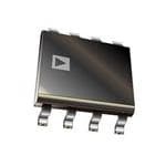
| 描述 | IC OPAMP GP 700KHZ RRO 8SOIC精密放大器 Prec RRO SGL Supply Dual 100uV Max |
| 产品分类 | Linear - Amplifiers - Instrumentation, OP Amps, Buffer Amps集成电路 - IC |
| 品牌 | Analog Devices |
| 产品手册 | |
| 产品图片 |
|
| rohs | 符合RoHS无铅 / 符合限制有害物质指令(RoHS)规范要求 |
| 产品系列 | 放大器 IC,精密放大器,Analog Devices OP727ARZ- |
| 数据手册 | |
| 产品型号 | OP727ARZ |
| 产品培训模块 | http://www.digikey.cn/PTM/IndividualPTM.page?site=cn&lang=zhs&ptm=30008http://www.digikey.cn/PTM/IndividualPTM.page?site=cn&lang=zhs&ptm=26202 |
| 产品目录页面 | |
| 产品种类 | 精密放大器 |
| 供应商器件封装 | 8-SOIC |
| 共模抑制比—最小值 | 120 dB |
| 关闭 | No |
| 包装 | 管件 |
| 压摆率 | 0.2 V/µs |
| 双重电源电压 | 1.5 V to 15 V |
| 商标 | Analog Devices |
| 增益带宽生成 | 0.7 MHz |
| 增益带宽积 | 700kHz |
| 安装类型 | 表面贴装 |
| 安装风格 | SMD/SMT |
| 封装 | Tube |
| 封装/外壳 | 8-SOIC(0.154",3.90mm 宽) |
| 封装/箱体 | SOIC-8 |
| 工作温度 | -40°C ~ 85°C |
| 工作电源电压 | 3 V to 30 V |
| 工厂包装数量 | 98 |
| 放大器类型 | 通用 |
| 最大双重电源电压 | 15 V |
| 最大工作温度 | + 85 C |
| 最小双重电源电压 | 1.5 V |
| 最小工作温度 | - 40 C |
| 标准包装 | 98 |
| 电压-电源,单/双 (±) | 2.7 V ~ 30 V, ±1.35 V ~ 15 V |
| 电压-输入失调 | 30µV |
| 电压增益dB | 113.98 dB |
| 电流-电源 | 320µA |
| 电流-输入偏置 | 5nA |
| 电流-输出/通道 | 30mA |
| 电源电压-最大 | 30 V |
| 电源电压-最小 | 3 V |
| 电源电流 | 320 uA |
| 电源类型 | Single, Dual |
| 电路数 | 2 |
| 系列 | OP727 |
| 视频文件 | http://www.digikey.cn/classic/video.aspx?PlayerID=1364138032001&width=640&height=505&videoID=2245193153001http://www.digikey.cn/classic/video.aspx?PlayerID=1364138032001&width=640&height=505&videoID=2245193159001 |
| 转换速度 | 0.2 V/us |
| 输入偏压电流—最大 | 10 nA |
| 输入电压范围—最大 | 14 V |
| 输入补偿电压 | 30 uV |
| 输出电流 | 30 mA |
| 输出类型 | Rail to Rail Output |
| 通道数量 | 2 Channel |


- 商务部:美国ITC正式对集成电路等产品启动337调查
- 曝三星4nm工艺存在良率问题 高通将骁龙8 Gen1或转产台积电
- 太阳诱电将投资9.5亿元在常州建新厂生产MLCC 预计2023年完工
- 英特尔发布欧洲新工厂建设计划 深化IDM 2.0 战略
- 台积电先进制程称霸业界 有大客户加持明年业绩稳了
- 达到5530亿美元!SIA预计今年全球半导体销售额将创下新高
- 英特尔拟将自动驾驶子公司Mobileye上市 估值或超500亿美元
- 三星加码芯片和SET,合并消费电子和移动部门,撤换高东真等 CEO
- 三星电子宣布重大人事变动 还合并消费电子和移动部门
- 海关总署:前11个月进口集成电路产品价值2.52万亿元 增长14.8%


PDF Datasheet 数据手册内容提取
a Precision Micropower Single-Supply Operational Amplifiers OP777/OP727/OP747 FEATURES FUNCTIONAL BLOCK DIAGRAMS Low Offset Voltage: 100 (cid:2)V Max 8-Lead MSOP 14-Lead SOIC Low Input Bias Current: 10nA Max (RM-8) (R-14) Single-Supply Operation: 3.0 V to 30 V Dual-Supply Operation: (cid:3)1.5 V to (cid:3)15 V Low Supply Current: 300(cid:2)A/Amp Max NC 1 8 NC Unity Gain Stable (cid:4)IN OP777 V+ OUT A 1 14 OUT D (cid:5)IN OUT –IN A 2 13 –IN D No Phase Reversal V(cid:4) 4 5 NC (cid:5)IN A 3 12 (cid:5)IN D NC = NO CONNECT OP747 APPLICATIONS V(cid:5) 4 TOP VIEW 11 V– Current Sensing (Shunt) 8-Lead SOIC (cid:5)IN B 5 (Not to Scale) 10 (cid:5)IN C Line or Battery-Powered Instrumentation (R-8) –IN B 6 9 –IN C Remote Sensors OUT B 7 8 OUT C Precision Filters OP727 SOIC Pin-Compatible with LT1013 NC 1 OP777 8 NC GENERAL DESCRIPTION (cid:4)IN 2 7 V+ 14-Lead TSSOP (RU-14) The OP777, OP727, and OP747 are precision single , dual, +IN 3 6 OUT V(cid:4) 4 5 NC and quad rail-to-rail output single- supply amplifiers featuring micropower operation and rail-to-rail output ranges. These NC = NO CONNECT OUT A 1 14 OUT D amplifiers provide improved performance over the industry -standard –IN A 2 13 –IN D OP07 with ±15 V supplies, and offer the further advantage of true 8-Lead TSSOP (cid:5)IN A 3 12 (cid:5)IN D single-supply operation down to3.0 V , and smaller package OP747 (RU-8) V(cid:5) 4 TOP VIEW 11 V– options than any other high-voltage precision bipolar amplifier. (cid:5)IN B 5 (Not to Scale) 10 (cid:5)IN C Outputs are stable with capacitive loads of over 500 pF. Supply current is less than 300 μA per amplifier at 5 V. 500 Ω series resis- OUT A 1 8 V(cid:5) –IN B 6 9 –IN C tors protect the inputs, allowing input signal levels several volts above –IN A 2 OP727 7 OUT B OUT B 7 8 OUT C the positive supply without phase reversal. (cid:5)IN A 3 (NToOt Pto V SIEcaWle) 6 –IN B Applications for these amplifiers include both line-powered and V– 4 5 (cid:5)IN B portable instrumentation, remote sensor signal conditioning, and precision filters. 8-Lead SOIC The OP777, OP727, and OP747 are specified over the extended (R-8) industrial (–40°C to +85°C) temperature range. The OP777, single, is available in 8-lead MSOP and 8-lead SOIC packages. The OP747, quad, is available in 14-lead TSSOP and narrow (cid:5)IN A 1 8 –IN A 14-lead SO packages. Surface-mount devices in TSSOP and MSOP V– 2 OP727 7 OUT A TOP VIEW packages are available in tape and reel only. (cid:5)IN B 3 (Not to Scale) 6 V(cid:5) –IN B 4 5 OUT B The OP727, dual, is available in 8-lead TSSOP and 8-lead SOIC packages. The OP727 8-lead SOIC pin configuration NOTE:THIS PIN CONFIGURATION DIFFERS differs from the standard 8-lead operational amplifier pinout. FROM THE STANDARD 8-LEAD OPERATIONAL AMPLIFIER PINOUT. SIMILAR LOW POWER PRODUCTS Supply Voltage/ Supply Current 1.8 V/1 μA 1.8 V/20 μA 1.8 V/25 μA 1.8 V/50 μA 2.5 V/1 mA 3.0 V/200 μA 4 V/215 μA Single AD8500 ADA4051-1 AD8505 AD8603/AD8613 ADA4528-1 Dual AD8502 ADA4051-2 AD8506 AD8607/AD8617 ADA4091-2 AD8622 Quad AD8504 AD8508 AD8609/AD8619 ADA4091-4 AD8624 REV.D Information furnished by Analog Devices is believed to be accurate and reliable. However, no responsibility is assumed by Analog Devices for its use, nor for any infringements of patents or other rights of third parties that One Technology Way, P.O. Box 9106, Norwood, MA 02062-9106, U.S.A. may result from its use. No license is granted by implication or otherwise Tel: 781/329-4700 www.analog.com under any patent or patent rights of Analog Devices. Fax: 781/461-3113 © Analog Devices, Inc., 2011
OP777/OP727/OP747–SPECIFICATIONS ELECTRICAL CHARACTERISTICS (@ V = 5.0 V, V = 2.5 V, T = 25(cid:6)C unless otherwise noted.) S CM A Parameter Symbol Conditions Min Typ Max Unit INPUT CHARACTERISTICS Offset Voltage OP777 V +25(cid:2)C < T < +85(cid:2)C 20 100 μV OS A –40°C < T < +85°C 50 200 μV A Offset Voltage OP727/OP747 +25(cid:2)C < T < +85(cid:2)C 30 160 μV A –40°C < T < +85°C 60 300 μV A Input Bias Current I –40°C < T < +85°C 5.5 11 nA B A Input Offset Current I –40°C < T < +85°C 0.1 2 nA OS A Input Voltage Range 0 4 V Common-Mode Rejection Ratio CMRR V = 0 V to 4 V 104 110 dB CM Large Signal Voltage Gain A R = 10 kΩ, V = 0.5 V to 4.5 V 300 500 V/mV VO L O Offset Voltage Drift OP777 ΔV /ΔT –40°C < T < +85°C 0.3 1.3 μV/°C OS A Offset Voltage Drift OP727/OP747 ΔV /ΔT –40°C < T < +85°C 0.4 1.5 μV/°C OS A OUTPUT CHARACTERISTICS Output Voltage High V I = 1 mA, –40°C to +85°C 4.88 4.91 V OH L Output Voltage Low V I = 1 mA, –40°C to +85°C 126 140 mV OL L Output Circuit I V < 1 V ±10 mA OUT DROPOUT POWER SUPPLY Power Supply Rejection Ratio PSRR V = 3 V to 30 V 120 130 dB S Supply Current/Amplifier OP777 I V = 0 V 220 270 μA SY O –40°C < T < +85°C 270 320 μA A Supply Current/Amplifier OP727/OP747 V = 0 V 235 290 μA O –40°C < T < +85°C 290 350 μA A DYNAMIC PERFORMANCE Slew Rate SR R = 2 kΩ 0.2 V/μs L Gain Bandwidth Product GBP 0.7 MHz NOISE PERFORMANCE Voltage Noise e p-p 0.1 Hz to 10 Hz 0.4 μV p-p n Voltage Noise Density e f = 1 kHz 15 nV/√Hz n Current Noise Density i f = 1 kHz 0.13 pA/√Hz n NOTES Typical specifications: >50% of units perform equal to or better than the “typical” value. Specifications subject to change without notice. –2– REV. D
OP777/OP727/OP747 ELECTRICAL CHARACTERISTICS (@ (cid:3)15 V, V = 0 V, T = 25(cid:6)C unless otherwise noted.) CM A Parameter Symbol Conditions Min Typ Max Unit INPUT CHARACTERISTICS Offset Voltage OP777 V +25°C < T < +85°C 30 100 μV OS A –40°C < T < +85°C 50 200 μV A Offset Voltage OP727/OP747 V +25°C < T < +85°C 30 160 μV OS A –40°C < T < +85°C 50 300 μV A Input Bias Current I –40°C < T < +85°C 5 10 nA B A Input Offset Current I –40°C < T < +85°C 0.1 2 nA OS A Input Voltage Range –15 +14 V Common-Mode Rejection Ratio CMRR V = –15 V to +14 V 110 120 dB CM Large Signal Voltage Gain A R = 10 kΩ, V = –14.5 V to +14.5 V 1,000 2,500 V/mV VO L O Offset Voltage Drift OP777 ΔV /ΔT –40°C < T < +85°C 0.3 1.3 μV/°C OS A Offset Voltage Drift OP727/OP747 ΔV /ΔT –40°C < T < +85°C 0.4 1.5 μV/°C OS A OUTPUT CHARACTERISTICS Output Voltage High V I = 1 mA, –40°C to +85°C +14.9 +14.94 V OH L Output Voltage Low V I = 1 mA, –40°C to +85°C –14.94 –14.9 V OL L Output Circuit I ±30 mA OUT POWER SUPPLY Power Supply Rejection Ratio PSRR V = ±1.5 V to ±15 V 120 130 dB S Supply Current/Amplifier OP777 I V = 0 V 300 350 μA SY O –40°C < T < +85°C 350 400 μA A Supply Current/Amplifier OP727/747 V = 0 V 320 375 μA O –40°C < T < +85°C 375 450 μA A DYNAMIC PERFORMANCE Slew Rate SR R = 2 kΩ 0.2 V/μs L Gain Bandwidth Product GBP 0.7 MHz NOISE PERFORMANCE Voltage Noise e p-p 0.1 Hz to 10 Hz 0.4 μV p-p n Voltage Noise Density e f = 1 kHz 15 nV/√Hz n Current Noise Density i f = 1 kHz 0.13 pA/√Hz n Specifications subject to change without notice. REV. D –3–
OP777/OP727/OP747 ABSOLUTE MAXIMUM RATINGS1, 2 Package Type (cid:7) 3 (cid:7) Unit JA JC Supply Voltage . . . . . . . . . . . . . . . . . . . . . . . . . . . . . . . . . 36 V IDnipffuetr eVnotilatal gIen p. u. t. V. .o l.t .a g. e. . .. .. .. .. .. .. .. .. .. .. .– .V .S . – ±5 SVu tpop +lyV VS o+l t5a gVe 88--LLeeaadd MSOSIOCP ( R(R)M) 119508 4443 °°CC//WW Output Short-Circuit Duration to GND . . . . . . . . . Indefinite 8-Lead TSSOP (RU) 240 43 °C/W Storage Temperature Range 14-Lead SOIC (R) 120 36 °C/W RM, R, RU Packages . . . . . . . . . . . . . . . . –65°C to +150°C 14-Lead TSSOP (RU) 180 35 °C/W Operating Temperature Range NOTES OP777/OP727/OP747 . . . . . . . . . . . . . . . –40°C to +85°C 1Absolute maximum ratings apply at 25°C, unless otherwise noted. Junction Temperature Range 2Stresses above those listed under Absolute Maximum Ratings may cause perma- RM, R, RU Packages . . . . . . . . . . . . . . . . –65°C to +150°C nent damage to the device. This is a stress rating only; functional operation of the Lead Temperature Range (Soldering, 60 sec) . . . . . . . 300°C device at these or any other conditions above those listed in the operational sections of this specification is not implied. Exposure to absolute maximum rating Electrostatic Discharge (Human Body Model) . . . . 2000 V max conditions for extended periods may affect device reliability. 3θ is specified for worst-case conditions, i.e., θ is specified for device soldered in JA JA circuit board for surface-mount packages. CAUTION ESD (electrostatic discharge) sensitive device. Electrostatic charges as high as 4000V readily WARNING! accumulate on the human body and test equipment and can discharge without detection. Although the OP777/OP727/OP747 features proprietary ESD protection circuitry, permanent damage may occur on devices subjected to high-energy electrostatic discharges. Therefore, proper ESD ESD SENSITIVE DEVICE precautions are recommended to avoid performance degradation or loss of functionality. –4– REV. D
Typical Performance Characteristics–OP777/OP727/OP747 220 220 30 200 VVSCYM == (cid:3)0V15V 200 VVSCYM == 52V.5V VVSCYM == (cid:3)0V15V S 180 TA = 25(cid:6)C S 180 TA = 25(cid:6)C S 25 TA = (cid:4)40(cid:6)C TO +85(cid:6)C ER 160 ER 160 ER FI FI FI 20 LI 140 LI 140 LI P P P F AM 120 F AM 120 F AM 15 O 100 O 100 O R R R E 80 E 80 E B B B 10 UM 60 UM 60 UM N N N 40 40 5 20 20 0 0 0 (cid:4)100(cid:4)80(cid:4)60(cid:4)40(cid:4)20 0 20 40 60 80 100 (cid:4)100(cid:4)80(cid:4)60(cid:4)40(cid:4)20 0 20 40 60 80 100 0 0.2 0.4 0.6 0.8 1.0 1.2 OFFSET VOLTAGE – (cid:2)V OFFSET VOLTAGE – (cid:2)V INPUT OFFSET DRIFT – (cid:2)V/(cid:6)C TPC 1.OP777 Input Offset Voltage TPC 2.OP777 Input Offset Voltage TPC 3.OP777 Input Offset Voltage Distribution Distribution Drift Distribution 200 600 600 118600 VTVASC YM= = =– 4(cid:3)00V1(cid:6)5CV TO +85(cid:6)C 500 VTVASC YM= = =2 5(cid:3)0(cid:6)V1C5V S500 TVVASC YM= = =2 552(cid:6)V.C5V s s R mplifier114200 mplifier400 PLIFIE400 A A M TITY – 10800 TITY – 300 R OF A300 N N E A A200 B200 U 60 U M Q Q U 40 N 100 100 20 0 0 0 0.10.20.30.40.50.60.70.80.91.01.11.2 –120 –80 –40 0 40 80 120 –120 –80 –40 0 40 80 120 TCVOS – (cid:2)V/(cid:6)C (cid:2)V OFFSET VOLTAGE – (cid:2)V TPC 4.OP727/OP747 Input Offset TPC 5.OP747 Input Offset Voltage TPC 6.OP747 Input Offset Voltage Voltage Drift (TCV Distribution) Distribution Distribution OS 600 600 30 S500 VTVASC YM= = =2 552(cid:6)V.C5V S 500 VTVASC YM= = =2 5(cid:3)0(cid:6)V1C5V S 25 VVTASC YM= = =2 5(cid:3)0(cid:6)V1C5V R R R E E E PLIFI400 PLIFI 400 PLIFI 20 M M M OF A300 OF A 300 OF A 15 R R R BE200 BE 200 BE 10 M M M U U U N N N 100 100 5 0 0 0 (cid:4)140(cid:4)120 (cid:4)80 (cid:4)40 0 40 80 120 (cid:4)140(cid:4)120 (cid:4)80 (cid:4)40 0 40 80 120 3 4 5 6 7 8 OFFSET VOLTAGE – (cid:2)V OFFSET VOLTAGE – (cid:2)V INPUT BIAS CURRENT – nA TPC 7. OP727 Input Offset Voltage TPC 8. OP727 Input Offset Voltage TPC 9.Input Bias Current Distribution Distribution Distribution REV. D –5–
OP777/OP727/OP747 10k 10k 6 TVAS == 2(cid:3)51(cid:6)5CV VTAS == 255V(cid:6)C VSY = (cid:3)15V 1k 1k 5 E – mV100 SINK E – mV100 NT – nA 4 G G E A A R T SOURCE T R OL 10 OL 10 SINK CU 3 UTPUT V 1.0 UTPUT V 1.0 SOURCE UT BIAS 2 O O P (cid:8) (cid:8) N 0.1 0.1 I 1 0 0 0 0.001 0.01 0.1 1 10 100 0.001 0.01 0.1 1 10 100 (cid:4)60(cid:4)40(cid:4)20 0 20 40 60 80 100120140 LOAD CURRENT – mA LOAD CURRENT – mA TEMPERATURE –(cid:6)C TPC 10.Output Voltage to Supply TPC 11.Output Voltage to Supply TPC 12.Input Bias Current vs. Rail vs. Load Current Rail vs. Load Current Temperature 500 350 140 400 300 TA = 25(cid:6)C 120 VCSLYO A=D (cid:3) =1 05V 300 ISY+ (VSY = (cid:3)15V) 100 RLOAD = (cid:2)SUPPLY CURRENT – A(cid:4)(cid:4)(cid:4)2121300000000000 IISSYY(cid:4)+ ((VVSSYY == 55VV)) (cid:2)SUPPLY CURRENT – A 211205050000 OPEN-LOOP GAIN – dB–24268000000 49112050382505PHASE SHIFT – Degrees (cid:4)400 ISY(cid:4) (VSY = (cid:3)15V) 50 –40 270 (cid:4)500 0 –60 (cid:4)60(cid:4)40(cid:4)20 0 20 40 60 80 100120 140 0 5 10 15 20 25 30 35 10 100 1k 10k 100k 1M 10M 100M TEMPERATURE –(cid:6)C SUPPLY VOLTAGE – V FREQUENCY –Hz TPC 13.Supply Current vs. TPC 14.Supply Current vs. Supply TPC 15.Open Loop Gain and Temperature Voltage Phase Shift vs. Frequency 140 VSY = 5V 60 VSY = (cid:3)15V 60 VSY = 5V 120 CLOAD = 0 50 CLOAD = 0 50 CLOAD = 0 OPEN-LOOP GAIN – dB–12042680000000 RLOAD = 49112050382505 PHASE SHIFT – Degrees CLOSED-LOOP GAIN – dB(cid:4)(cid:4)4321120000000 AAVV == +(cid:4)110AV = (cid:4)100 RLOAD = 2k(cid:9) CLOSED-LOOP GAIN – dB(cid:4)(cid:4)4321120000000 AAVV == +(cid:4)110AV = (cid:4)100 RLOAD = 2k(cid:9) –40 270 (cid:4)30 (cid:4)30 –60100 1k 10k 100k 1M 10M 100M (cid:4)401k 10k 100k 1M 10M 100M (cid:4)401k 10k 100k 1M 10M 100M FREQUENCY – Hz FREQUENCY –Hz FREQUENCY –Hz TPC 16.Open Loop Gain and TPC 17.Closed Loop Gain vs. TPC 18.Closed Loop Gain vs. Phase Shift vs. Frequency Frequency Frequency –6– REV. D
OP777/OP727/OP747 300 300 270 AV = 1 VSY = 5V 270 VSY = (cid:3)15V RVSLY = = 2 (cid:3)k(cid:9)2.5V (cid:9) 240 (cid:9) 240 CL = 300pF TPUT IMPEDANCE – 21111852900000 TPUT IMPEDANCE – 21111852900000 AV = 1 VOLTAGE – 1V/DIV AV = 1 0V OU 60 AV = 10 AV = 100 OU 60 AV = 100 AV = 10 30 30 0 0 100 1k 10k 100k 1M 10M 100M 100 1k 10k 100k 1M 10M 100M TIME – 100(cid:2)s/DIV FREQUENCY – Hz FREQUENCY – Hz TPC 19.Output Impedance vs. TPC 20.Output Impedance vs. TPC 21.Large Signal Transient Frequency Frequency Response VSY = (cid:3)15V VSY = (cid:3)2.5V VSY = (cid:3)15V RL = 2k(cid:9) CL = 300pF CL = 300pF CL = 300pF RL = 2k(cid:9) RL = 2k(cid:9) V VIN = 100mV V VIN = 100mV V/DIV AV = 1 mV/DI mV/DI GE – 10V E – 50 AV = 1 E – 50 AV = 1 A G G T A A OL LT LT V O O V V TIME – 100(cid:2)s/DIV TIME – 10(cid:2)s/DIV TIME – 10(cid:2)s/DIV TPC 22.Large Signal Transient TPC 23.Small Signal Transient TPC 24.Small Signal Transient Response Response Response 40 35 VSY = (cid:3)2.5V VSY = (cid:3)15V INPUT % 35 RL = 2k(cid:9) % 30 RL = 2k(cid:9) +200mV OT – 30 VIN = 100mV OT – VIN = 100mV 0V O (cid:5)OS O 25 ERSH 25 ERSH 20 +OS VRSLY = = 1 (cid:3)0k1(cid:9)5V AL OV 20 (cid:4)OS AL OV 15 (cid:4)OS AVIVN == (cid:4)20100m0V GN 15 GN 0V LL SI 10 LL SI 10 (cid:4)10V A A M M S 5 S 5 OUTPUT 0 0 1 10 100 1k 1 10 100 1k 10k TIME – 40(cid:2)s/DIV CAPACITANCE – pF CAPACITANCE – pF TPC 25.Small Signal Overshoot TPC 26.Small Signal Overshoot TPC 27.Negative Overvoltage vs. Load Capacitance vs. Load Capacitance Recovery REV. D –7–
OP777/OP727/OP747 200mV INPUT INPUT INPUT 0V 0V 0V (cid:4)200mV VRVASILVNY === = 1(cid:4)(cid:4) (cid:3)012k100(cid:9)500VmV VRVASILVNY === = 1(cid:4)2 (cid:3)001k200(cid:9).m05VV (cid:4)200mV VRAVSILVNY === = 1(cid:4)(cid:4) (cid:3)012k200(cid:9).005mVV 10V 0V 2V OUTPUT 0V (cid:4)2V 0V OUTPUT OUTPUT TIME – 40(cid:2)s/DIV TIME – 40(cid:2)s/DIV TIME – 40(cid:2)s/DIV TPC 28.Positive Overvoltage TPC 29.Negative Overvoltage TPC 30.Positive Overvoltage Recovery Recovery Recovery 140 140 INPUT VS = (cid:3)15V VSY = (cid:3)2.5V VSY = (cid:3)15V AV = 1 120 120 V OUTPUT 100 100 DI V/ B B E – 5 R – d 80 R – d 80 G R R A M 60 M 60 T C C L O V 40 40 20 20 0 0 TIME – 400(cid:2)s/DIV 10 100 1k 10k 100k 1M 10M 10 100 1k 10k 100k 1M 10M FREQUENCY – Hz FREQUENCY – Hz TPC 31.No Phase Reversal TPC 32.CMRR vs. Frequency TPC 33.CMRR vs. Frequency 140 140 VSY = (cid:3)2.5V VSY = (cid:3)15V VSY = 5V 120 120 GAIN = 10M +PSRR 100 100 V B (cid:4)PSRR B +PSRR V/DI d 80 d 80 1 R – R – (cid:4)PSRR E – R R G S 60 S 60 A P P T L O 40 40 V 20 20 0 0 10 100 1k 10k 100k 1M 10M 10 100 1k 10k 100k 1M 10M TIME – 1s/DIV FREQUENCY – Hz FREQUENCY – Hz TPC 34.PSRR vs. Frequency TPC 35.PSRR vs. Frequency TPC 36.0.1 Hz to 10 Hz Input Voltage Noise –8– REV. D
OP777/OP727/OP747 90 90 VSY = (cid:3)15V VSY = (cid:3)15V VSY = (cid:3)2.5V GAIN = 10M Hz80 Hz 80 V/ V/ – n70 – n 70 DIV TY TY V/ SI60 SI 60 1 N N GE – E DE50 E DE 50 VOLTA AGE NOIS3400 AGE NOIS 3400 T T L L VO20 VO 20 10 10 TIME – 1s/DIV 0 100 200 300 400 500 0 100 200 300 400 500 FREQUENCY – Hz FREQUENCY – Hz TPC 37.0.1 Hz to 10 Hz Input TPC 38.Voltage Noise Density TPC 39.Voltage Noise Density Voltage Noise 40 40 50 VOLTAGE NOISE DENSITY – nV/ Hz 1122335050505 VSY = (cid:3)15V VOLTAGE NOISE DENSITY – nV/ Hz 1122335050505 VSY = (cid:3)2.5V SHORT CIRCUIT CURRENT – mA (cid:4)(cid:4)(cid:4)(cid:4)43142213000000000 IVISSSCCY+(cid:4) = 5V 0 0 (cid:4)50 0 500 1k 1.5k 2.0k 2.5k 0 500 1k 1.5k 2.0k 2.5k (cid:4)60(cid:4)40(cid:4)20 0 20 40 60 80 100120 140 FREQUENCY – Hz FREQUENCY – Hz TEMPERATURE –(cid:6)C TPC 40.Voltage Noise Density TPC 41.Voltage Noise Density TPC 42.Short Circuit Current vs. Temperature 50 4.95 160 A 40 VSY = (cid:3)15V VILS =Y 1=m 5AV 150 VILS =Y 1=m 5AV SHORT CIRCUIT CURRENT – m(cid:4)(cid:4)(cid:4)3122130000000 IISSCC+(cid:4) OUTPUT VOLTAGE HIGH – V 44444.....9999924310 OUTPUT VOLTAGE LOW – mV11111012349000000 (cid:4)40 80 (cid:4)50(cid:4)60(cid:4)40(cid:4)20 0 20 40 60 80 100120 140 4.8(cid:4)960(cid:4)40(cid:4)20 0 20 40 60 80 100120 140 7(cid:4)060(cid:4)40(cid:4)20 0 20 40 60 80 100120 140 TEMPERATURE –(cid:6)C TEMPERATURE – (cid:6)C TEMPERATURE – (cid:6)C TPC 43.Short Circuit Current vs. TPC 44.Output Voltage High vs. TPC 45.Output Voltage Low vs. Temperature Temperature Temperature REV. D –9–
OP777/OP727/OP747 14.964 (cid:4)14.930 1.5 – V1144..996602 VILS =Y 1=m (cid:3)A15V – V(cid:4)14.935 IVLS =Y 1=m (cid:3)A15V 1.0 VVTASC YM= = =2 5(cid:3)0(cid:6)V1C5V H W HIG14.958 LO(cid:4)14.940 0.5 OLTAGE 1144..995546 OLTAGE (cid:4)14.945 (cid:2)V – VOS 0 UT V14.952 UT V(cid:4)14.950 (cid:8)(cid:4)0.5 P14.950 P UT UT O14.948 O(cid:4)14.955 (cid:4)1.0 14.946 14.944 (cid:4)14.960 (cid:4)1.5 (cid:4)60(cid:4)40(cid:4)20 0 20 40 60 80 100120 140 (cid:4)60(cid:4)40(cid:4)20 0 20 40 60 80 100120 140 0 0.5 1.0 1.5 2.0 2.5 3.0 3.5 4.0 4.5 5.0 TEMPERATURE – (cid:6)C TEMPERATURE – (cid:6)C TIME –Minutes TPC 46.Output Voltage High vs. TPC 47.Output Voltage Low vs. TPC 48.Warm-Up Drift Temperature Temperature BASIC OPERATION The OP777/OP727/OP747 amplifier uses a precision Bipolar PNP input stage coupled with a high-voltage CMOS output stage. This enables this amplifier to feature an input voltage V DI VOUT range which includes the negative supply voltage (often ground- V/ m in single-supply applications) and also swing to within 1 mV of the 00 1 output rails. Additionally, the input voltage range extends to within E – 0V 1 V of the positive supply rail. The epitaxial PNP input structure TAG VIN provides high breakdown voltage, high gain, and an input bias cur- OL V rent figure comparable to that obtained with a “Darlington” input stage amplifier but without the drawbacks (i.e., severe penalties for input voltage range, offset, drift and noise). The PNP input structure also greatly lowers the noise and reduces the dc input error terms. TIME – 0.2ms/DIV Supply Voltage Figure 1.Input and Output Signals with V < 0 V CM The amplifiers are fully specified with a single 5 V supply and, due to design and process innovations, can also operate with a supply 100k(cid:9) voltage from 3.0 V up to 30 V. This allows operation from most split supplies used in current industry practice, with the advantage 100k(cid:9) +3V of substantially increased input and output voltage ranges over conventional split-supply amplifiers. The OP777/OP727/OP747 (cid:4)0.27V series is specified with (V = 5 V, V– = 0 V and V = 2.5 V 100k(cid:9) SY CM which is most suitable for single-supply application. With PSRR of OP777/ 130 dB (0.3 μV/V) and CMRR of 110 dB (3 μV/V) offset is mini- 100k(cid:9) OP727/ OP747 mally affected by power supply or common-mode voltages. Dual (cid:4)0.1V supply, ±15 V operation is also fully specified. VIN = 1kHz at 400mV p-p Input Common-Mode Voltage Range Figure 2.OP777/OP727/OP747 Configured as a Differ- The OP777/OP727/OP747 is rated with an input common-mode ence Amplifier Operating at V < 0 V voltage which extends from the minus supply to within 1 V of the CM positive supply. However, the amplifier can still operate with input voltages slightly below V . In Figure 2, OP777/OP727/OP747 is EE configured as a difference amplifier with a single supply of 3.0 V and negative dc common-mode voltages applied at the inputs terminals. A 400 mV p-p input is then applied to the noninverting input. It can be seen from the graph below that the output does not show any distortion. Micropower operation is maintained by using large input and feedback resistors. –10– REV. D
OP777/OP727/OP747 Input Over Voltage Protection When the input of an amplifier is more than a diode drop below VSY = (cid:3)15V V , or above V , large currents will flow from the substrate VIN EE CC (V–) or the positive supply (V+), respectively, to the input pins which can destroy the device. In the case of OP777/OP727/ DIV VOUT OP747, differential voltages equal to the supply voltage will not 5V/ – cause any problem (see Figure 3). OP777/OP727/OP747 has E G built-in 500 Ω internal current limiting resistors, in series with the A T L inputs, to minimize the chances of damage. It is a good practice to O V keep the current flowing into the inputs below 5 mA. In this con- text it should also be noted that the high breakdown of the input transistors removes the necessity for clamp diodes between the inputs of the amplifier, a feature that is mandatory on many preci- TIME – 400(cid:2)s/DIV sion op amps. Unfortunately, such clamp diodes greatly interfere with many application circuits such as precision rectifiers and Figure 4.No Phase Reversal comparators. The OP777/OP727/OP747 series is free from such Output Stage limitations. The CMOS output stage has excellent (and fairly symmetric) output drive and with light loads can actually swing to within 1 mV of both 30V supply rails. This is considerably better than similar amplifiers featuring (so-called) rail-to-rail bipolar output stages. OP777/ OP727/OP747 is stable in the voltage follower configuration and responds to signals as low as 1 mV above ground in single supply OP777/ operation. V p-p = 32V OP727/ OP747 Figure 3a.Unity Gain Follower 3.0V TO 30V VOUT = 1mV VSY = (cid:3)15V VIN = 1mV OP777/ VIN OP727/ OP747 DIV VOUT Figure 5.Follower Circuit V/ 5 – E G A T L O V V DI V/ m 5 2 – TIME – 400(cid:2)s/DIV E G Figure 3b.Input Voltage Can Exceed the Supply Voltage LTA 1.0mV O Without Damage V Phase Reversal Many amplifiers misbehave when one or both of the inputs are forced beyond the input common-mode voltage range. Phase TIME – 10(cid:2)s/DIV reversal is typified by the transfer function of the amplifier effectively reversing its transfer polarity. In some cases this can cause lockup in Figure 6.Rail-to-Rail Operation servo systems and may cause permanent damage or nonrecoverable Output Short Circuit parameter shifts to the amplifier. Many amplifiers feature compensa- The output of the OP777/OP727/OP747 series amplifier is protected tion circuitry to combat these effects, but some are only effective for from damage against accidental shorts to either supply voltage, the inverting input. Additionally, many of these schemes only work provided that the maximum die temperature is not exceeded on a for a few hundred millivolts or so beyond the supply rails. OP777/ long-term basis (see Absolute Maximum Rating section). Current of OP727/OP747 has a protection circuit against phase reversal up to 30 mA does not cause any damage. when one or both inputs are forced beyond their input common- A Low-Side Current Monitor mode voltage range. It is not recommended that the parts be In the design of power supply control circuits, a great deal of design continuously driven more than 3 V beyond the rails. effort is focused on ensuring a pass transistor’s long-term reliability over a wide range of load current conditions. As a result, monitoring REV. D –11–
OP777/OP727/OP747 and limiting device power dissipation is of prime importance in 15V these designs. Figure 7 shows an example of 5 V, single-supply current monitor that can be incorporated into the design of a voltage regulator with foldback current limiting or a high current power 1k(cid:9) REF 2N2222 supply with crowbar protection. The design capitalizes on the 192 1/4 OP747 OP777’s common-mode range that extends to ground. Current 12k(cid:9) R2 is monitored in the power supply return where a 0.1 Ω shunt 4 3 20k(cid:9) R1 R1 +15V resistor, R , creates a very small voltage drop. The voltage at the SENSE inverting terminal becomes equal to the voltage at the noninverting VO terminal through the feedback of Q1, which is a 2N2222 or equiva- +15V R(1+(cid:10)) R 1/4 OP747 lent NPN transistor. This makes the voltage drop across R1 equal to (cid:4)15V the voltage drop across RSENSE. Therefore, the current through Q1 1/4 OP747 VO = RR 12 VREF (cid:10) becomes directly proportional to the current through RSENSE, and (cid:10) =(cid:8)R the output voltage is given by: (cid:4)15V R Figure 9. Linear Response Bridge ⎛R2 ⎞ V =5V −⎜ ×R ×I ⎟ A single-supply current source is shown in Figure 10. Large resistors OUT ⎝R1 SENSE L⎠ are used to maintain micropower operation. Output current can be adjusted by changing the R2B resistor. Compliance voltage is: The voltage drop across R2 increases with I increasing, so V L OUT decreases with higher supply current being sensed. For the element V ≤ V − V L SAT S values shown, the V is 2.5 V for return current of 1 A. OUT 10pF 5V 3.0V TO 30V 100k(cid:9) R2 = 2.49k(cid:9) VOUT 100k(cid:9) OP777 Q1 R1 = 100k(cid:9) 5V R2B 2.7k(cid:9) 10pF IO R2 = R2A + R2B R2A + R1 = 100(cid:9) 0.1(cid:9) OP777RETURN TO IO = R 1 (cid:11)R 2 R 2 B VS 97.3k(cid:9) VL R(cid:4)LOAD RSENSE GROUND = 1mA (cid:4) 11mA Figure 7. A Low-Side Load Current Monitor Figure 10. Single-Supply Current Source The OP777/OP727/OP747 is very useful in many bridge applica- A single-supply instrumentation amplifier using one OP727 tions. Figure 8 shows a single-supply bridge circuit in which its amplifier is shown in Figure 11. For true difference R3/R4 = output is linearly proportional to the fractional deviation ((cid:3)) of R1/R2. The formula for the CMRR of the circuit at dc is CMRR = the bridge. Note that (cid:3) = ΔR/R. 20 × log (100/(1–(R2 × R3)/(R1× R4)). It is common to specify the accuracy of the resistor network in terms of resistor-to-resistor = 300 percentage mismatch. We can rewrite the CMRR equation to 15V VO = A R 1 2 (cid:11) R V 2 R E F (cid:10) + 2.5V reflect this CMRR = 20 × log (10000/% Mismatch). The key to 2 high CMRR is a network of resistors that are well matched from 1/4 OP747 REF 6 RG = 10k(cid:9)(cid:10) = (cid:8)RR11 the perspective of both resistive ratio and relative drift. It should 2 192 be noted that the absolute value of the resistors and their absolute 2.5V 1M(cid:9) 10.1k(cid:9) drift are of no consequence. Matching is the key. CMRR is 100 dB 4 3 1M(cid:9) REF 0.1(cid:2)F with 0.1% mismatched resistor network. To maximize CMRR, 192 15V one of the resistors such as R4 should be trimmed. Tighter match- 4 3 R1 R1(1+(cid:10)) 10.1k(cid:9) 15V ing of two op amps in one package (OP727) offers a significant V1 boost in performance over the triple op amp configuration. 1/4 OP747 VO R1(1+(cid:10)) R1 1/4 OP747 R3 = 10.1k(cid:9) R2 = 1M(cid:9) R2 3.0V TO 30V V2 R4 = 1M(cid:9) 3.0V TO 30V R1 = 10.1k(cid:9) Figure 8. Linear Response Bridge, Single Supply In systems where dual supplies are available, the circuit of Figure 1/2 OP727 VO V1 1/2 OP727 9 could be used to detect bridge outputs that are linearly related V2 to the fractional deviation of the bridge. VO = 100 (V2 (cid:4) V1) 0.02mV V1 (cid:4) V2 290mV 2mV VOUT 29V USE MATCHED RESISTORS Figure 11. Single-Supply Micropower Instrumentation Amplifier –12– REV. D
OP777/OP727/OP747 OUTLINE DIMENSIONS 3.20 3.00 2.80 8 5 5.15 3.20 4.90 3.00 4.65 2.80 1 4 PIN1 IDENTIFIER 0.65BSC 0.95 15°MAX 0.85 1.10MAX 0.75 0.80 0.15 0.40 6° 0.23 0.55 0.05 0.25 0° 0.09 0.40 COPLANARITY B 0.10 COMPLIANTTOJEDECSTANDARDSMO-187-AA 10-07-2009- Figure 12. 8-Lead Mini Small Outline Package [MSOP] (RM-8) Dimensions shown in millimeters 5.00(0.1968) 4.80(0.1890) 8 5 4.00(0.1574) 6.20(0.2441) 3.80(0.1497) 1 4 5.80(0.2284) 1.27(0.0500) 0.50(0.0196) 45° BSC 1.75(0.0688) 0.25(0.0099) 0.25(0.0098) 1.35(0.0532) 8° 0.10(0.0040) 0° COPLANARITY 0.51(0.0201) 1.27(0.0500) 0.10 SEATING 0.31(0.0122) 0.25(0.0098) 0.40(0.0157) PLANE 0.17(0.0067) COMPLIANTTOJEDECSTANDARDSMS-012-AA CONTROLLINGDIMENSIONSAREINMILLIMETERS;INCHDIMENSIONS A (RINEFPEARREENNCTEHEOSNELSY)AANRDEARROEUNNODTEDA-POPFRFOMPIRLLIAIMTEETFEORREUQSUEIVINALDEENSTIGSNF.OR 012407- Figure 13. 8-Lead Standard Small Outline Package [SOIC_N] Narrow Body (R-8) Dimensions shown in millimeters and (inches) REV. D –13–
OP777/OP727/OP747 3.10 3.00 2.90 8 5 4.50 4.40 6.40 BSC 4.30 1 4 PIN 1 0.65 BSC 0.15 1.20 0.05 MAX 8° COPLANARITY 0.30 SEATING 0.20 0° 0.75 0.10 0.19 PLANE 0.60 0.09 0.45 COMPLIANT TO JEDEC STANDARDS MO-153-AA Figure 14. 8-Lead Thin Shrink Small Outline Package [TSSOP] (RU-8) Dimensions shown in millimeters 8.75 (0.3445) 8.55 (0.3366) 14 8 4.00 (0.1575) 6.20 (0.2441) 3.80 (0.1496) 1 7 5.80 (0.2283) 1.27 (0.0500) 0.50 (0.0197) BSC 45° 1.75 (0.0689) 0.25 (0.0098) 0.25 (0.0098) 1.35 (0.0531) 8° 0.10 (0.0039) 0° COPLANARITY SEATING 0.10 0.51 (0.0201) PLANE 0.25 (0.0098) 1.27 (0.0500) 0.31 (0.0122) 0.17 (0.0067) 0.40 (0.0157) COMPLIANTTO JEDEC STANDARDS MS-012-AB CONTROLLING DIMENSIONSARE IN MILLIMETERS; INCH DIMENSIONS A (RINEFPEARREENNCTEH EOSNELSY)AANRDE ARROEU NNODETDA-POPFRFO MPIRLILAIMTEE TFEORR EUQSUEI VINA LDEENSTIGS NF.OR 060606- Figure 15. 14-Lead Standard Small Outline Package [SOIC_N] Narrow Body (R-14) Dimensions shown in millimeters and (inches) –14– REV. D
OP777/OP727/OP747 5.10 5.00 4.90 14 8 4.50 4.40 6.40 BSC 4.30 1 7 PIN 1 0.65 BSC 1.05 1.20 1.00 MAX 0.20 0.80 0.09 0.75 0.15 8° 0.60 0.05 0.30 SPELAATNIENG 0° 0.45 COPLANARITY 0.19 0.10 A COMPLIANT TO JEDEC STANDARDS MO-153-AB-1 061908- Figure 16. 14-Lead Thin Shrink Small Outline Package [TSSOP] (RU-14) Dimensions shown in millimeters ORDERING GUIDE Model1 Temperature Range Package Description Package Option Branding OP727AR –40°C to +85°C 8-Lead SOIC_N R-8 OP727AR-REEL –40°C to +85°C 8-Lead SOIC_N R-8 OP727AR-REEL7 –40°C to +85°C 8-Lead SOIC_N R-8 OP727ARUZ –40°C to +85°C 8-Lead TSSOP RU-8 OP727ARUZ-REEL –40°C to +85°C 8-Lead TSSOP RU-8 OP727ARZ –40°C to +85°C 8-Lead SOIC_N R-8 OP727ARZ-REEL –40°C to +85°C 8-Lead SOIC_N R-8 OP727ARZ-REEL7 –40°C to +85°C 8-Lead SOIC_N R-8 OP747ARU –40°C to +85°C 14-Lead TSSOP RU-14 OP747ARU-REEL –40°C to +85°C 14-Lead TSSOP RU-14 OP747ARUZ –40°C to +85°C 14-Lead TSSOP RU-14 OP747ARUZ-REEL –40°C to +85°C 14-Lead TSSOP RU-14 OP747ARZ –40°C to +85°C 14-Lead SOIC R-14 OP747ARZ-REEL –40°C to +85°C 14-Lead SOIC R-14 OP747ARZ-REEL7 –40°C to +85°C 14-Lead SOIC R-14 OP777ARMZ –40°C to +85°C 8-Lead MSOP RM-8 A1A OP777ARMZ-REEL –40°C to +85°C 8-Lead MSOP RM-8 A1A OP777ARZ –40°C to +85°C 8-Lead SOIC_N R-8 OP777ARZ-REEL –40°C to +85°C 8-Lead SOIC_N R-8 OP777ARZ-REEL7 –40°C to +85°C 8-Lead SOIC_N R-8 1 Z = RoHS Compliant Part. REV. D –15–
OP777/OP727/OP747 REVISION HISTORY 10/11—Rev. C to Rev. D Changed Single Supply Operation from 2.7 V to 30 V to 3.0 V to 30 V ...................................................................................... 1 Changed Dual Supply Operation from ±1.35 V to ±15 V to ±1.5 V to ±15 V ................................................................................. 1 Changes to General Description Section ...................................... 1 Added Similar Low Power Products Table .................................... 1 Changes to Supply Voltage Section, Input Common-Mode Voltage Range Section, and Figure 1 ............................................ 10 Changes to Figure 5 ........................................................................ 11 Changes to Figure 10 and Figure 11 ............................................. 12 Updated Outline Dimensions ....................................................... 13 Changes to Ordering Guide .......................................................... 15 9/01—Rev. B to Rev. C Addition of text to Applications Section ....................................... 1 Addition of 8-Lead SOIC (R-8) Package ....................................... 1 Addition of text to General Description ........................................ 1 Addition of package to Ordering Guide ........................................ 2 ©2011 Analog Devices, Inc. All rights reserved. Trademarks and registered trademarks are the property of their respective owners. D02051-0-10/11(D) –16– REV. D
Mouser Electronics Authorized Distributor Click to View Pricing, Inventory, Delivery & Lifecycle Information: A nalog Devices Inc.: OP727AR-REEL7 OP727ARZ OP777ARZ-REEL OP747ARZ-REEL OP747ARUZ OP747ARZ OP777ARMZ OP777ARMZ-REEL OP727ARUZ OP777ARZ-REEL7 OP727AR OP747ARUZ-REEL OP747ARU OP727ARZ-REEL OP747ARU-REEL OP727AR-REEL OP747ARZ-REEL7 OP777ARZ OP727ARZ-REEL7 OP727ARUZ-REEL