ICGOO在线商城 > TLE4913
 Datasheet下载
- 型号: TLE4913
- 制造商: Infineon
- 库位|库存: xxxx|xxxx
- 要求:
| 数量阶梯 | 香港交货 | 国内含税 |
| +xxxx | $xxxx | ¥xxxx |
查看当月历史价格
查看今年历史价格
TLE4913产品简介:
ICGOO电子元器件商城为您提供TLE4913由Infineon设计生产,在icgoo商城现货销售,并且可以通过原厂、代理商等渠道进行代购。 提供TLE4913价格参考以及InfineonTLE4913封装/规格参数等产品信息。 你可以下载TLE4913参考资料、Datasheet数据手册功能说明书, 资料中有TLE4913详细功能的应用电路图电压和使用方法及教程。
| 参数 | 数值 |
| 产品目录 | |
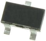
| 描述 | IC LP HALL SWTCH MCPWR SC59-3板机接口霍耳效应/磁性传感器 IC LP HALL SWTCH MCPWR OMNIPOLAR |
| 产品分类 | 磁性传感器 - 霍尔效应,数字开关,线性,罗盘 (IC)磁性传感器 |
| 品牌 | Infineon Technologies |
| 产品手册 | |
| 产品图片 |
|
| rohs | 符合RoHS无铅 / 符合限制有害物质指令(RoHS)规范要求 |
| 产品系列 | 板机接口霍耳效应/磁性传感器,Infineon Technologies TLE4913- |
| mouser_ship_limit | 该产品可能需要其他文件才能进口到中国。 |
| 数据手册 | http://www.infineon.com/dgdl/TLE4913_Data_Sheet_2006_03_16.pdf?folderId=db3a304412b407950112b408e8c90004&fileId=db3a304412b407950112b409121100af |
| 产品型号 | TLE4913 |
| 产品目录页面 | |
| 产品种类 | 板机接口霍耳效应/磁性传感器 |
| 供应商器件封装 | SC-59 |
| 其它名称 | TLE4913INDKR |
| 包装 | Digi-Reel® |
| 商标 | Infineon Technologies |
| 安装风格 | SMD/SMT |
| 封装 | Reel |
| 封装/外壳 | TO-236-3,SC-59,SOT-23-3 |
| 封装/箱体 | SOT-23-3 |
| 工作温度 | -40°C ~ 85°C |
| 工作电源电压 | 2.5 V or 3.3 V or 5 V |
| 工厂包装数量 | 3000 |
| 感应范围 | 3.5mT 跳闸, 2.7mT 释放 |
| 最大工作温度 | + 85 C |
| 最大输出电流 | 2 mA |
| 最小工作温度 | - 40 C |
| 标准包装 | 1 |
| 特性 | - |
| 电压-电源 | 2.4 V ~ 5.5 V |
| 电流-电源 | 1.1mA |
| 电流-输出(最大值) | 2mA |
| 类型 | Omnipolar Switch |
| 系列 | TLE4913 |
| 输出类型 | 数字,开路集电极 |
| 零件号别名 | SP000013490 TLE4913HTSA1 |


- 商务部:美国ITC正式对集成电路等产品启动337调查
- 曝三星4nm工艺存在良率问题 高通将骁龙8 Gen1或转产台积电
- 太阳诱电将投资9.5亿元在常州建新厂生产MLCC 预计2023年完工
- 英特尔发布欧洲新工厂建设计划 深化IDM 2.0 战略
- 台积电先进制程称霸业界 有大客户加持明年业绩稳了
- 达到5530亿美元!SIA预计今年全球半导体销售额将创下新高
- 英特尔拟将自动驾驶子公司Mobileye上市 估值或超500亿美元
- 三星加码芯片和SET,合并消费电子和移动部门,撤换高东真等 CEO
- 三星电子宣布重大人事变动 还合并消费电子和移动部门
- 海关总署:前11个月进口集成电路产品价值2.52万亿元 增长14.8%


PDF Datasheet 数据手册内容提取
Low Power Hall Switch TLE 4913 Features • Micro power design • 2.4 V to 5.5 V battery operation • High sensitivity and high stability of the magnetic switching points • High resistance to mechanical stress • Digital output signal • Switching for both poles of a magnet (omnipolar) SC59-3-x • Not suitable for automotive application Functional Description The TLE4913 is an Integrated Hall-Effect Sensor designed specifically to meet the requirements of low-power devices. e.g. as an On/Off switch in Cellular Flip-Phones, with battery operating voltages of 2.4V (cid:150) 5.5V. Precise magnetic switching points and high temperature stability are achieved through the unique design of the internal circuit. An onboard clock scheme is used to reduce the average operating current of the IC. During the operate phase the IC compares the actual magnetic field detected with the internally compensated switching points. The output Q is switched at the end of each operating phase. During the Stand-by phase the output stage is latched and the current consumption of the device reduced to some (cid:181)A. The IC switching behaviour is Omnipolar, i.e. it can be switched on with either the North or South pole of a magnet. Type Marking Ordering Code Package 13s TLE 4913 Q62705K 619 SC 59-3-x 013 Data Sheet 1 V 2.2, 2004-03-09
Top View GND Sensitive Area 3 month 13 sm y year 1 2 V Q S AEP02801_13 Figure 1 Pin Configuration (top view) Pin Definitions and Functions Pin Symbol Function 1 V Supply Voltage S 2 Q Open Drain Input 3 Gnd Ground Data Sheet 2 V 2.2, 2004-03-09
V S 1 Bias and Compensation Circuits Oscillator Active Error Threshold & Compensation Generator Sequencer 3 GND Comparator Hall with Probe Hysteresis 2 Decision Q Latch Logic Chopped Amplifier AEB02800_13 Figure 2 Block Diagram Circuit Description The Low Power Hall IC Switch comprises a Hall probe, bias generator, compensation circuits, oscillator, output latch and an n-channel open drain output transistor. The bias generator provides currents for the Hall probe and the active circuits. Compensation circuits stabilize the temperature behavior and reduce technology variations. The Active Error Compensation rejects offsets in signal stages and the influence of mechanical stress to the Hall probe caused by molding and soldering processes and other thermal stresses in the package. This chopper technique together with the threshold generator and the comparator ensures high accurate magnetic switching points. Very low power consumption is achieved with a timing scheme controlled by an oscillator and a sequencer. This circuitry activates the sensor for 50 (cid:181)s (typical operating time) sets the output state after sequential questioning of the switch points and latches it with the beginning of the following standby phase (max. 200 ms). In the standby phase the average current is reduced to typical 4 (cid:181)A. Because of the long standby time compared to the operating time the overall averaged current is only slightly higher than the standby current. The output transistor can sink up to 1 mA with a maximal saturation voltage V . QSAT Data Sheet 3 V 2.2, 2004-03-09
Absolute Maximum Ratings Parameter Symbol Limit Values Unit Notes min. max. Supply Voltage V (cid:150) 0.3 5.5 V S Supply Current I (cid:150) 1 2.5 mA S Output Voltage V (cid:150) 0.3 5.5 V Q Output Current I (cid:150) 1 2 mA Q Junction temperature T (cid:150) 40 150 (cid:176)C j Storage temperature T (cid:150) 40 150 (cid:176)C S Magnetic Flux Density B (cid:150) unlimited mT Thermal Resistance R (cid:150) 35 K/W th JA P-SC59-3-x Note: Stresses above those listed here may cause permanent damage to the device. Exposure to absolute maximum rating conditions for extended periods may affect device reliability. ESD Protection Human Body Model (HBM) tests according to: EOS/ESD Association Standard S5.1-1993 and Mil. Std. 883D method 3015.7 Parameter Symbol Limit Values Unit Notes Min. Max. ESD Voltage V – 4 kV R = 1.5 kΩ, ESD C = 100 pF; T = 25 (cid:176)C Data Sheet 4 V 2.2, 2004-03-09
Operating Range Parameter Symbol Limit Values Unit Notes Min. typ. max. Supply voltage V 2.4 2.7 5.5 V 1) S Output voltage V (cid:150) 0.3 2.7 5.5 V Q Ambient Temperature T (cid:150) 40 25 85 (cid:176)C A 1) A Ceramic Bypass Capacitor of 100 nF at V to GND is highly recommended. S AC/DC Characteristics Parameter Symbol Limit Values Unit Notes Min. typ. Max. Averaged Supply Current I 1 4 20 (cid:181)A SAVG Averaged Supply I 0.5 1.1 2.5 mA SOPAVG Current during Operating Time Transient Peak Supply I (cid:150) (cid:150) 2.5 mA t < 100 ns SOPT Current during Operating Time Supply Current I 1 3.5 20 (cid:181)A SSTB during Standby Time Output Saturation Voltage V (cid:150) 0.13 0.4 V I = 1 mA QSAT Q Output Leakage Current I (cid:150) 0.01 1 (cid:181)A QLEAK Output Rise Time t (cid:150) 0.5 1 (cid:181)s R = 2.7 kΩ; r L C = 10 pF L Output Fall Time t (cid:150) 0.1 1 (cid:181)s R = 2.7 kΩ; f L C = 10 pF L Operating Time t 15 50 93 1) 2) (cid:181)s op Standby Time t (cid:150) 130 240 3) ms stb Duty Cycle t / t (cid:150) 0.039 (cid:150) % op stb Start-up Time of IC t (cid:150) 6 12 (cid:181)s 4) stu 1) for V =3.5V the max. Operating Time t = 85(cid:181)s S op max 2) includes the Start-up Time t stu 3) for V =3.5V the max. Standby Time t = 220ms S stb max 4) initial power on time. V must be applied in this time ( typ. 6(cid:181)s to max. 12(cid:181)s ) to get already a valid output S state after the first operating phase (typ. 56(cid:181)s). For rise times of V > 12(cid:181)s, the output state is valid after the S second operating phase (includes one standby phase), e.g. happens only when the battery in flip phones is changed. Data Sheet 5 V 2.2, 2004-03-09
Magnetic Characteristics Parameter Symbol Limit Values Unit Notes min. typ. max. Operate Points B 2 3.5 5 mT 1) OPS (Output on) B (cid:150) 5 (cid:150) 3.5 - 2 mT OPN Release Points B 1,2 2.7 4.2 mT 1) RPS (Output off) B (cid:150) 4.2 (cid:150) 2.6 - 1,2 mT RPN Hysteresis B 0.2 0.8 1,6 mT HYS 1) Positive magnetic fields are related to the approach of a magnetic south pole to the branded side of package Note: The listed AC/DC and magnetic characteristics are ensured over the operating range of the integrated circuit. Typical characteristics specify mean values expected over the production spread. If not other specified, typical characteristics apply at T = 25 (cid:176)C j and V = 2.7 V S Data Sheet 6 V 2.2, 2004-03-09
I Operating S Time I SOPAVG Standby Time I SAVG I t t SSTB op stb 50 µs 130 ms Latch t Output AET02802-17 Figure 3 Timing Diagram V as function of the applied B-Field Q Figure 4 Output (cid:150) Signal TLE 4913 Data Sheet 7 V 2.2, 2004-03-09
All curves reflect typical values at the given parameters for T in °C and V in V. A S Magnetic Switching Points versus Magnetic Switching Points versus Temperature (V =2.7V) Supply Voltage V (T =20(cid:176)C) S S A B[mT] B[mT] 5 5 4 4 B OPS BOPS 3 3 BRPS BRPS 2 2 1 1 0 0 -1 -1 -2 -2 B B RPN RPN -3 -3 B OPN BOPN -4 -4 -5 -5 -40 -20 0 20 40 60 80 100 2.5 3 3.5 4 4.5 5 5.5 6 T [(cid:176)C] VS [V] Supply current I during Operating Supply current I during Operating SOPAVG SOPAVG Time versus Temperature (V =2.7V) Time versus Supply Voltage V (T =20(cid:176)C) S S A 2.5 2.5 I [mA] I [mA] 2 2 1.5 I SOPAVG 1.5 1 I SOPAVG 1 0.5 0.5 0 -40 -20 0 20 40 60 80 100 2.5 3 3.5 4 4.5 5 5.5 6 T [(cid:176)C] V S [V] Data Sheet 8 V 2.2, 2004-03-09
Supply current I during Standby Supply current I during Standby SSTB SSTB Time versus Temperature (V =2.7V) Time versus Supply Voltage V (T =20(cid:176)C) S S A 20 20 I [(cid:181)A] I [(cid:181)A] 18 18 16 16 14 14 12 12 10 10 8 8 I SSTB 6 6 I SSTB 4 4 2 2 0 0 -40 -20 0 20 40 60 80 100 2.5 3 3.5 4 4.5 5 5.5 6 T [(cid:176)C] V [V] S Output Saturation voltage V Standby Time t versus Temperature QSAT stb versus Temperature ( I =1mA ) (V = 2.7V) Q S 200 180 t [ms] V[mV] 170 V 160 QSAT 160 140 150 120 100 140 80 130 60 120 40 t stb 110 20 0 100 -40 -20 0 20 40 60 80 100 -40 -20 0 20 40 60 80 100 T [(cid:176)C] T [(cid:176)C] Data Sheet 9 V 2.2, 2004-03-09
Top View Marking on P-SC 59-3-x package corresponds to pin 1 of device 3 13 sym 1 2 Position in Tape: pin 1 opposite of feed hole side Direction of Unreeling Package Pieces / Reel ∅Reel P-SC59-3-x 3.000 180 mm Figure 5 Marking and Tape Loading Orientation Figure 6 Foot Print Reflow Soldering Data Sheet 10 V 2.2, 2004-03-09
Package Dimensions P-SC 59-3-x - Package coplanarity : 0.10mm Sorts of Packing Package outlines for tubes, trays etc. are contained in our Data Book (cid:148)Package Information(cid:148). SMD = Surface Mounted Device Data Sheet 11 V 2.2, 2004-03-09
TLE4913 Revision History: 2004-03-09 V 2.2 Previous Version: 2003-07-16 Page Subjects (major changes since last revision) 4 ESD Level adapted to –4 kV For questions on technology, delivery and prices please contact the Infineon Technologies Offices in Germany or the Infineon Technologies Companies and Representatives worldwide: see our webpage at http://www.infineon.com We Listen to Your Comments Any information within this document that you feel is wrong, unclear or missing at all? Your feedback will help us to continuously improve the quality of this document. Please send your proposal (including a reference to this document) to: feedback.sensors@infineon.com Edition 2002-08-22 Published by Infineon Technologies AG St.-Martin-Strasse 53 D-81541 M(cid:252)nchen ' Infineon Technologies AG 2000 All Rights Reserved. Attention please! The information herein is given to describe certain components and shall not be considered as warranted characteristics. Terms of delivery and rights to technical change reserved. We hereby disclaim any and all warranties, including but not limited to warranties of non-infringement, regarding circuits, descriptions and charts stated herein. Infineon Technologiesis an approved CECC manufacturer. Information For further information on technology, delivery terms and conditions and prices please contact your nearest Infineon Technologies Office in Germany or our Infineon Technologies Representatives worldwide (see address list). Warnings Due to technical requirements components may contain dangerous substances. For information on the types in question please contact your nearest Infineon Technologies Office. Infineon Technologies Components may only be used in life-support devices or systems with the express written approval of Infineon Technologies, if a failure of such components can reasonably be expected to cause the failure of that life-support device or system, or to affect the safety or effectiveness of that device or system. Life support devices or systems are intended to be implanted in the human body, or to support and/or maintain and sustain and/or protect human life. If they fail, it is reasonable to assume that the health of the user or other persons may be endangered. Data Sheet 12 V 2.2, 2004-03-09
Mouser Electronics Authorized Distributor Click to View Pricing, Inventory, Delivery & Lifecycle Information: I nfineon: TLE4913