ICGOO在线商城 > 射频/IF 和 RFID > RF 天线 > ANT-868-CHP-T
 Datasheet下载
- 型号: ANT-868-CHP-T
- 制造商: LINX TECHNOLOGIES
- 库位|库存: xxxx|xxxx
- 要求:
| 数量阶梯 | 香港交货 | 国内含税 |
| +xxxx | $xxxx | ¥xxxx |
查看当月历史价格
查看今年历史价格
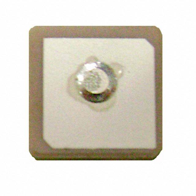
ANT-868-CHP-T产品简介:
ICGOO电子元器件商城为您提供ANT-868-CHP-T由LINX TECHNOLOGIES设计生产,在icgoo商城现货销售,并且可以通过原厂、代理商等渠道进行代购。 ANT-868-CHP-T价格参考。LINX TECHNOLOGIESANT-868-CHP-T封装/规格:RF 天线, 868MHz 蓝牙,Wi-Fi,Zigbee™ 芯片 RF 天线 863MHz ~ 873MHz 0.5dBi 焊接 表面贴装。您可以下载ANT-868-CHP-T参考资料、Datasheet数据手册功能说明书,资料中有ANT-868-CHP-T 详细功能的应用电路图电压和使用方法及教程。
Linx Technologies Inc. 的 ANT-868-CHP-T 是一款适用于 868 MHz 频段的 RF(射频)天线,主要用于短距离无线通信场景。以下是其典型应用场景:

1. 工业自动化:该天线可安装在传感器、控制器或网关设备上,用于数据采集与监控系统(SCADA)、远程控制以及工厂内的无线通信。

2. 智能家居:ANT-868-CHP-T 可集成到家庭自动化设备中,例如智能照明、温控器、安防系统等,支持低功耗无线连接,实现远程操控和状态反馈。

3. 物联网 (IoT):这款天线广泛应用于基于 LoRa、Sigfox 或其他专有协议的 IoT 设备中,适合需要稳定信号传输的小型化终端产品。

4. 无线报警系统:用于烟雾探测器、门窗传感器等安全设备,提供可靠的无线信号传输以确保警报信息及时传递至接收端。

5. 环境监测:在气象站、水质检测仪或其他环境监测设备中使用,帮助收集并发送温度、湿度、风速等数据至中央处理单元。

6. 医疗健康设备:如便携式心率监测仪、血糖仪等,通过无线方式将患者数据上传至云端或医生端进行分析。

7. 农业技术:应用于精准农业领域,比如土壤湿度传感器、灌溉控制系统等,助力优化资源利用效率。

8. 资产追踪与物流管理:为 RFID 标签阅读器或 GPS 跟踪装置配备此天线,提升货物运输过程中的定位精度及信息更新频率。

ANT-868-CHP-T 具有紧凑设计、高增益性能和良好的匹配特性,非常适合对体积敏感且要求高效能无线通信的产品开发项目。
| 参数 | 数值 |
| 产品目录 | |
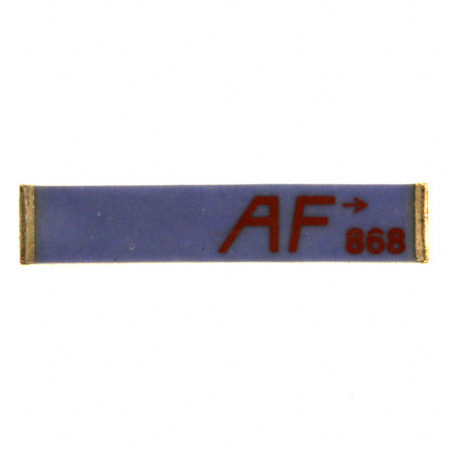
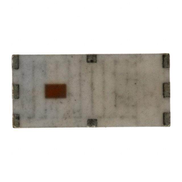
| 描述 | ANTENNA CHIP 868MHZ CERAMIC SMD |
| 产品分类 | |
| 品牌 | Linx Technologies Inc |
| 数据手册 | |
| 产品图片 |
|
| 产品型号 | ANT-868-CHP-T |
| rohs | 无铅 / 符合限制有害物质指令(RoHS)规范要求 |
| 产品系列 | CHP - Antenna Factor |
| VSWR | 2 |
| 其它名称 | ANT-868-CHP |
| 包装 | 带卷 (TR) |
| 增益 | 0.5dBi |
| 天线类型 | 芯片,1/4 波 |
| 安装类型 | 表面贴装 |
| 应用说明 | |
| 标准包装 | 3,000 |
| 端接 | 表面贴装型 |
| 频带数 | 1 |
| 频率 | 868MHz |
| 高度(最大值) | 0.067"(1.70mm) |


- 商务部:美国ITC正式对集成电路等产品启动337调查
- 曝三星4nm工艺存在良率问题 高通将骁龙8 Gen1或转产台积电
- 太阳诱电将投资9.5亿元在常州建新厂生产MLCC 预计2023年完工
- 英特尔发布欧洲新工厂建设计划 深化IDM 2.0 战略
- 台积电先进制程称霸业界 有大客户加持明年业绩稳了
- 达到5530亿美元!SIA预计今年全球半导体销售额将创下新高
- 英特尔拟将自动驾驶子公司Mobileye上市 估值或超500亿美元
- 三星加码芯片和SET,合并消费电子和移动部门,撤换高东真等 CEO
- 三星电子宣布重大人事变动 还合并消费电子和移动部门
- 海关总署:前11个月进口集成电路产品价值2.52万亿元 增长14.8%
PDF Datasheet 数据手册内容提取
Ultra Compact Chip Antenna Data Guide
Table of Contents 1 Description 1 Features 2 Applications 2 Ordering Information 2 Electrical Specifications 3 Footprints 3 Pin Configuration 4 Theory of Operation 4 Layout Considerations 5 Microstrip Details 6 Assembly Considerations 8 Test Boards 9 VSWR Graphs 10 Tape Dimensions 12 Reel Dimensions 13 Mismatch Conversion Table
Ultra Compact Chip Antenna Data Guide Description The exciting ANT-***-CHP family is among the world’s smallest high-performance chip antennas. They are ideal for embedding in wireless products including 2.4 xxx Bluetooth, 802.11, Home RF, ZigBee and other popular standards. These tiny antennas use advanced Low Temperature Co-fired Ceramic (LTCC) technology and proprietary elements to achieve superior size and performance characteristics. The entire family is com- Figure 1: 2.4GHz Dimensions patible with hand and reflow-assembly. Excellent electrical specifications, stability, and outstanding cost-effectiveness make CHP Series antennas th2e.4 logical choice xxx for a wide variety of applications. Features • Incredibly compact SMD package • Superior LTCC technology Figure 2: 868MHz and 916MHz Dimensions • 50Ω characteristic impedance • Low loss • Wide bandwidth • Favorable linear polarization 2.45GHz • > Unity gain • No external matching required 868MHz 916MHz • Highly stable over temperature & time Figure 3: Actual Sizes • Hand and reflow-assembly compatible • RoHS compliant • Cost-effective – 1 – Revised 8/8/12
Applications Footprints • Bluetooth • Data collection • 802.11 • Industrial process monitoring 0.260" 0.630" • ZigBee • Compact wireless products • Wireless PCMCIA cards • External antenna elimination 0.100" 0.130" • Telemetry Ordering Information 0.040" 0.040" Ordering Information Figure 6: 2.4GHz Footprint Figure 7: 868MHz and 916MHz Footprint Part Number Description ANT-868-CHP-x 868Mhz Chip Antenna Pin Configuration ANT-916-CHP-x 916MHz Chip Antenna ANT-2.45-CHP-x 2.45GHz Chip Antenna 1 2 x = "T" for tape/reel, "B" for bulk 2.4 All parts are RoHS compliant. Standard reel is 3,000pcs. (868/916MHz), 1,500pcs. (2.45GHz) Figure 8: Pin Configuration Quantities less than reel size are supplied in bulk. Pin Descriptions Figure 4: Ordering Information Pin Number Description Electrical Specifications Feed Termination 1 This pin connects to the transmitter or receiver. Specifications Solder Termination 2 This pin is soldered down for physical support only. There is no Parameter 2.45GHz 868MHz 916MHz electrical connection. Physical Dimensions (mm) 6.5(L) x 2.2(W) x 16.0(L) x 3.0(W) x 16.0(L) x 3.0(W) x Figure 9: Pin Configurations 1.0(H) 1.7(H) 1.7(H) Operating/Storage Temp –40 to +85°C –40 to +85°C –40 to +85°C Construction LTCC LTCC LTCC Electrical Center Frequency 2.45GHz 868MHz 916MHz Bandwidth 180MHz 10MHz 10MHz Wavelength ¼-wave ¼-wave ¼-wave Pattern Omni-directional Omni-direction Omni-directional Polarization Linear Linear Linear VSWR ≤2.0 (Max.) ≤2.0 (Max.) ≤2.0 (Max.) Maximum Gain +0.5dBi +0.5dBi +0.5dBi Impedance 50Ω 50Ω 50Ω Power Handling 3W (Max.) 3W (Max.) 3W (Max.) Figure 5: Ordering Information – 2 – – 3 –
Theory of Operation Microstrip Details The CHP Series antennas utilize Low Temperature Cofired Ceramic (LTCC) A transmission line is a medium whereby RF energy is transferred from technology to embed the antenna element into a ceramic substrate. one place to another with minimal loss. This is a critical factor, especially in Advances in this technology have resulted in materials that are extremely high-frequency products like Linx RF modules, because the trace lead- stable over time and temperature, producing an antenna that is highly ing to the module’s antenna can effectively contribute to the length of reliable across a wide range of applications. The high-frequency charac- the antenna, changing its resonant bandwidth. In order to minimize loss teristics of this technology enable exceptional performance in a very small and detuning, some form of transmission line between the antenna and package. The construction techniques for LTCC devices lends itself well to the module should be used unless the antenna can be placed very close favorable pricing in high volume. (<1/8in.) to the module. One common form of transmission line is a coax cable and another is the microstrip. This term refers to a PCB trace run- Layout Considerations ning over a ground plane that is designed to serve as a transmission line Proper layout is vital to ensure correct operation and optimum perfor- between the module and the antenna. The width is based on the desired mance. Improper placement of planes, traces, or system components will characteristic impedance of the line, the thickness of the PCB and the result in nulls or complete de-tuning. Ideally, the antenna will be mounted dielectric constant of the board material. For standard 0.062in thick FR-4 on the board in such a way as to allow an unobstructed field of view. board material, the trace width would be 111 mils. The correct trace width The area underneath the antenna must be free of components, traces, can be calculated for other widths and materials using the information in and planes. Components may be placed to the rear of the antenna in the Figure 11 and examples are provided in Figure 12. Software for calculating ground plane counterpoise area. The feed trace from the RF stage to the microstrip lines is also available on the Linx website. antenna must be a microstrip trace or coax transmission line and should be Trace kept as short as practical. Board The layout of our reference jigs is illustrated on the following pages. Ground plane While they demonstrate various aspects of a layout, it is not necessary to replicate them exactly. While your board size and layout may differ, it is important to recognize that the counterpoise plays an important role in resonance and stability since it acts, in essence, as part of the antenna. After your own layout is complete, the performance of the antenna in your specific product should be carefully checked using tools like a network analyzer. In some cases, the size of the product’s PCB, proximity of the case, or other factors may make a custom version of the antenna necessary. Contact Linx for more information. No electrical connection. Figure 11: Microstrip Formulas 4 For physical support only 2. No ground plane or traces Example Microstrip Calculations under the antenna Width / Height Effective Dielectric Characteristic Dielectric Constant PCB pads for the CHP Ratio (W / d) Constant Impedance (Ω) 4.80 1.8 3.59 50.0 Ground plane on bottom 4.00 2.0 3.07 51.0 layer for counterpoise 2.55 3.0 2.12 48.8 50-ohm microstrip line Figure 10: Layout Figure 12: Example Microstrip Calculations – 4 – – 5 –
Assembly Considerations Reflow Soldering Profile The antenna is RoHS Compliant and designed to support hand or 10 sec, max automated assembly. To avoid damage to the part, the reflow solder 260°C guidelines found below should be carefully followed. The antenna is single ended meaning that one pad is electrically connected while the other is for C) 230°C mechanical support only. The antenna terminals are not interchangeable ature (° 180°C so the polarity indicated in the Pin Configuration section must be observed er p during assembly. m e T 30 sec. Hand Soldering 60 sec. This antenna is designed for high-volume automated assembly, however, it may be successfully attached by hand assembly techniques. A hand-solder Preheating temperature of 225°C or lower should be used. Do not exceed a 10sec. heating time. Time (sec.) Figure 13: Reflow Soldering Profile Reflow Temperature Profile The single most critical stage in the automated assembly process is the Warning: Pay attention to the absolute maximum solder times. reflow process. The reflow profile below should be closely followed since excessive temperatures or transport times during reflow will irreparably Absolute Maximum Solder Times damage the antennas. Assembly personnel will need to pay careful Hand Solder Temperature: TX +225ºC for 10 seconds attention to the oven's profile to ensure that it meets the requirements Hand Solder Temperature: RX +225ºC for 10 seconds necessary to successfully reflow all components while still meeting the Recommended Solder Melting Point: +180ºC limits mandated by the antennas themselves. Reflow Oven: +225ºC max (see Figure 13) Figure 14: Absolute Maximum Solder Times – 6 – – 7 –
Test Boards VSWR Graphs 30 What is VSWR? The Voltage Standing Wave Ratio (VSWR) is a measurement of how well an antenna is matched to a source impedance, typically 50-ohms. It is calcu- 20 Ground Plane lated by measuring the voltage wave that is headed toward the load versus (Top and Bottom Layers) the voltage wave that is reflected back from the load. A perfect match will have a VSWR of 1:1. The higher the first number, the worse the match, and the more inefficient the system. Since a perfect match cannot ever be 50W Transmission Line obtained, some benchmark for performance needs to be set. In the case of 30 antenna VSWR, this is usually 2:1. At this point, 88.9% of the energy sent to the antenna by the transmitter is radiated into free space and 11.1% is either reflected back into the source or lost as heat on the structure of the 14 14 antenna. In the other direction, 88.9% of the energy recovered by the an- tenna is transferred into the receiver. As a side note, since the “:1” is always Figure 15. 2.4GHz Test Board implied, many data sheets will remove it and just display the first number. 3.30" 0.89" (84mm) (23mm) How to Read a VSWR Graph VSWR is usually displayed graphically versus frequency. The lowest point on the graph is the antenna’s operational center frequency. In most cases, 0.17" this will be different than the designed center frequency due to fabrication (23mm) tolerances. The VSWR at that point denotes how close to 50-ohms the an- 0.08" 1.50" (2mm) xxx (38mm) tenna gets. Linx specifies the recommended bandwidth as the range where the typical antenna VSWR is less than 2:1. VSWR 1.681 Reflected Power 3:1 25% Figure 16: 868MHz and 916MHz Test Board 2:1 11% 1:1 0% 2.4GHz 2.45GHz 2.5GHz Figure 17: 2.4GHz Typical VSWR VSWR 1.229 Reflected Power 3:1 25% 2:1 11% 1:1 0% 818MHz 868MHz 918MHz Figure 18: 868MHz and 916MHz Typical VSWR – 8 – – 9 –
Tape Dimensions D1 P5 P4 D2 T2 D1 P5 P4 D2 T2 P3 P2 P3 P2 W F W F 5° 1.2 P1 A0 P1 3.1 5° T4 T3 Figure 21: 868MHz and 916MHz Tape Dimensions T4 Figure 19: 2.4GHz Tape Dimensions 868MHz and 916MHz Tape Dimensions Symbol Dimension Tolerance Unit D1 1.50 ±0.10 mm 2.4GHz Tape Dimensions D2 1.50 ±0.10 mm Symbol Dimension Tolerance Unit F 10.6 ±0.10 mm A0 2.30 ±0.10 mm P1 8.00 ±0.10 mm ±0.10 D1 1.50 mm –0.00 P2 11.50 ±0.10 mm ±0.25 D2 1.50 mm P3 1.75 ±0.10 mm –0.00 P4 4.00 ±0.10 mm F 6.60 ±0.10 mm P5 2.00 ±0.10 mm P1 8.00 ±0.10 mm T2 0.30 ±0.05 mm P2 7.50 ±0.10 mm T3 3.30 ±0.10 mm P3 1.75 ±0.10 mm T4 1.90 ±0.10 mm P4 4.00 ±0.10 mm W 24.00 ±0.30 mm P5 2.00 ±0.10 mm T2 0.30 ±0.05 mm Figure 21: 868MHz and 916MHz Tape Dimensions Table T4 1.30 ±0.10 mm W 16.00 ±0.10 mm Figure 20: 2.4GHz Tape Dimensions Table – 1 0 – – 1 1 –
Reel Dimensions Mismatch Conversion Table W1 Mismatch Conversion Table VSWR Insertion Loss (dB) Power Transmitted (%) Power Reflected (%) 17.391 –6.87 20.57% 79.43% 11.610 –5.35 29.21% 70.79% 8.724 –4.33 36.90% 63.10% E 6.997 –3.59 43.77% 56.23% 5.848 –3.02 49.88% 50.12% B 5.030 –2.57 55.33% 44.67% C 4.419 –2.20 60.19% 39.81% 3.946 –1.90 64.52% 35.48% 3.570 –1.65 68.38% 31.62% 3.010 –1.26 74.88% 25.12% 2.615 –0.97 80.05% 19.95% 2.323 –0.75 84.15% 15.85% 2.100 –0.58 87.41% 12.59% A W 1.925 –0.46 90.00% 10.00% 1.433 –0.14 96.84% 3.15% Figure 22: Reel Dimensions 1.222 –0.04 99.00% 1.00% 1.119 –0.01 99.68% 0.32% Reel Dimensions 1.065 0.00 99.90% 0.10% Symbol 868/916MHz 2.45GHz Unit 1.034 0.00 99.97% 0.03% QTY per reel 3,000 1,500 pcs 1.020 0.00 99.99% 0.01% Tape width 24 16 mm A 330±1 180±1 mm Figure 24: Mismatch Conversion Table B 100±0.5 62±0.5 mm C 13±0.5 13±0.2 mm E 2.2±0.5 2.2±0.5 mm W 24±0.5 16±0.5 mm W1 28.9±0.2 20±0.2 mm Figure 23: Reel Dimensions Table – 1 2 – – 1 3 –
(This page is intentionally blank.) (This page is intentionally blank.)
Linx Technologies 159 Ort Lane Merlin, OR, US 97532 3090 Sterling Circle, Suite 200 Boulder, CO 80301 Phone: +1 541 471 6256 Fax: +1 541 471 6251 www.linxtechnologies.com Disclaimer Linx Technologies is continually striving to improve the quality and function of its products. For this reason, we reserve the right to make changes to our products without notice. The information contained in this Data Guide is believed to be accurate as of the time of publication. Specifications are based on representative lot samples. Values may vary from lot-to-lot and are not guaranteed. “Typical” parameters can and do vary over lots and application. Linx Technologies makes no guarantee, warranty, or representation regarding the suitability of any product for use in any specific application. It is Customer’s responsibility to verify the suitability of the part for the intended application. At Customer’s request, Linx Technologies may provide advice and assistance in designing systems and remote control devices that employ Linx Technologies RF products, but responsibility for the ultimate design and use of any such systems and devices remains entirely with Customer and/or user of the RF products. LINX TECHNOLOGIES DISCLAIMS ANY AND ALL WARRANTIES OF MERCHANTABILITY AND FITNESS FOR A PARTICULAR PURPOSE. IN NO EVENT SHALL LINX TECHNOLOGIES BE LIABLE FOR ANY CUSTOMER’S OR USER’S INCIDENTAL OR CONSEQUENTIAL DAMAGES ARISING OUT OF OR RELATED TO THE DESIGN OR USE OF A REMOTE CONTROL SYSTEM OR DEVICE EMPLOYING LINX TECHNOLOGIES RF PRODUCTS OR FOR ANY OTHER BREACH OF CONTRACT BY LINX TECHNOLOGIES. CUSTOMER AND/OR USER ASSUME ALL RISKS OF DEATH, BODILY INJURIES, OR PROPERTY DAMAGE ARISING OUT OF OR RELATED TO THE USE OF LINX TECHNOLOGIES RF PRODUCTS, INCLUDING WITH RESPECT TO ANY SERVICES PROVIDED BY LINX RELATED TO THE USE OF LINX TECHNOLOGIES RF PRODUCTS. LINX TECHNOLOGIES SHALL NOT BE LIABLE UNDER ANY CIRCUMSTANCES FOR A CUSTOMER’S, USER’S, OR OTHER PERSON’S DEATH, BODILY INJURY, OR PROPERTY DAMAGE ARISING OUT OF OR RELATED TO THE DESIGN OR USE OF A REMOTE CONTROL SYSTEM OR DEVICE EMPLOYING LINX TECHNOLOGIES RF PRODUCTS. The limitations on Linx Technologies’ liability are applicable to any and all claims or theories of recovery asserted by Customer, including, without limitation, breach of contract, breach of warranty, strict liability, or negligence. Customer assumes all liability (including, without limitation, liability for injury to person or property, economic loss, or business interruption) for all claims, including claims from third parties, arising from the use of the Products. Under no conditions will Linx Technologies be responsible for losses arising from the use or failure of the device in any application, other than the repair, replacement, or refund limited to the original product purchase price. Devices described in this publication may contain proprietary, patented, or copyrighted techniques, components, or materials. © 2012 Linx Technologies. All rights reserved. The stylized Linx logo, Wireless Made Simple, CipherLinx, WiSE and the stylized CL logo are trademarks of Linx Technologies.
Mouser Electronics Authorized Distributor Click to View Pricing, Inventory, Delivery & Lifecycle Information: L inx Technologies: ANT-2.45-CHP-B ANT-2.45-CHP-T AEK-2.45-CHP AEK-868-CHP ANT-868-CHP-B ANT-868-CHP-T AEK-916- CHP ANT-916-CHP-B ANT-916-CHP-T