ICGOO在线商城 > 集成电路(IC) > 线性 - 放大器 - 仪表,运算放大器,缓冲器放大器 > TLC27L4ACN
 Datasheet下载
- 型号: TLC27L4ACN
- 制造商: Texas Instruments
- 库位|库存: xxxx|xxxx
- 要求:
| 数量阶梯 | 香港交货 | 国内含税 |
| +xxxx | $xxxx | ¥xxxx |
查看当月历史价格
查看今年历史价格
TLC27L4ACN产品简介:
ICGOO电子元器件商城为您提供TLC27L4ACN由Texas Instruments设计生产,在icgoo商城现货销售,并且可以通过原厂、代理商等渠道进行代购。 TLC27L4ACN价格参考¥4.64-¥11.52。Texas InstrumentsTLC27L4ACN封装/规格:线性 - 放大器 - 仪表,运算放大器,缓冲器放大器, 通用 放大器 4 电路 14-PDIP。您可以下载TLC27L4ACN参考资料、Datasheet数据手册功能说明书,资料中有TLC27L4ACN 详细功能的应用电路图电压和使用方法及教程。
TLC27L4ACN 是 Texas Instruments(德州仪器)推出的一款低功耗、双通道运算放大器,属于线性放大器系列中的仪表、运算放大器和缓冲器放大器类别。该型号具有低静态电流和轨到轨输出特性,适用于多种低功耗应用场景。以下是其主要应用场景:

1. 电池供电设备
   TLC27L4ACN 的低功耗特性使其非常适合电池供电的便携式设备,例如手持测量仪器、无线传感器节点和便携式医疗设备。它能够延长电池寿命,同时保持稳定的信号放大性能。

2. 数据采集系统
   在数据采集系统中,TLC27L4ACN 可用于信号调理电路,对微弱的模拟信号进行放大和滤波处理。例如,它可以与模数转换器(ADC)配合使用,以提高信号分辨率和信噪比。

3. 工业自动化与控制
   该器件可用于工业自动化中的传感器信号放大。例如,在温度、压力或流量传感器的应用中,TLC27L4ACN 能够将传感器输出的小信号放大到适合后续处理的范围。

4. 医疗电子设备
   TLC27L4ACN 的低噪声和低功耗特性使其适用于医疗电子领域,如心电图(ECG)、脉搏血氧仪等设备中的信号放大。它能够在不影响精度的情况下处理生物电信号。

5. 音频信号处理
   在低功耗音频应用中,TLC27L4ACN 可用作前置放大器,对音频信号进行初步放大,确保信号不失真且功耗较低。例如,它可用于便携式音频播放器或语音识别设备。

6. 汽车电子
   由于其宽工作电压范围(2.7V 至 16V),TLC27L4ACN 可应用于汽车电子系统中的信号调理电路,例如车内传感器信号放大或音频信号处理。

7. 消费电子产品
   在需要低功耗和小尺寸设计的消费电子产品中,TLC27L4ACN 可用于信号放大和缓冲功能,例如智能家居设备、可穿戴设备等。

总之,TLC27L4ACN 凭借其低功耗、高稳定性和轨到轨输出特性,广泛适用于需要精确信号放大和低功耗设计的各种场景。
| 参数 | 数值 |
| -3db带宽 | - |
| 产品目录 | 集成电路 (IC)半导体 |
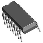
| 描述 | IC OPAMP GP 110KHZ 14DIP运算放大器 - 运放 LiNCMOS Quad |
| 产品分类 | Linear - Amplifiers - Instrumentation, OP Amps, Buffer Amps集成电路 - IC |
| 品牌 | Texas Instruments |
| 产品手册 | http://www.ti.com/litv/slos053c |
| 产品图片 |
|
| rohs | 符合RoHS无铅 / 符合限制有害物质指令(RoHS)规范要求 |
| 产品系列 | 放大器 IC,运算放大器 - 运放,Texas Instruments TLC27L4ACNLinCMOS™ |
| 数据手册 | |
| 产品型号 | TLC27L4ACN |
| PCN设计/规格 | |
| 产品目录页面 | |
| 产品种类 | 运算放大器 - 运放 |
| 供应商器件封装 | 14-PDIP |
| 共模抑制比—最小值 | 65 dB |
| 关闭 | No Shutdown |
| 其它名称 | 296-7382-5 |
| 包装 | 管件 |
| 单位重量 | 1 g |
| 压摆率 | 0.05 V/µs |
| 商标 | Texas Instruments |
| 增益带宽生成 | 0.085 MHz |
| 增益带宽积 | 110kHz |
| 安装类型 | 通孔 |
| 安装风格 | Through Hole |
| 封装 | Tube |
| 封装/外壳 | 14-DIP(0.300",7.62mm) |
| 封装/箱体 | PDIP-14 |
| 工作温度 | 0°C ~ 70°C |
| 工作电源电压 | 3 V to 16 V |
| 工厂包装数量 | 25 |
| 技术 | LinCMOS |
| 放大器类型 | 通用 |
| 最大工作温度 | + 70 C |
| 最小工作温度 | 0 C |
| 标准包装 | 25 |
| 电压-电源,单/双 (±) | 3 V ~ 16 V, ±1.5 V ~ 8 V |
| 电压-输入失调 | 900µV |
| 电流-电源 | 57µA |
| 电流-输入偏置 | 0.7pA |
| 电流-输出/通道 | 30mA |
| 电源电流 | 0.092 mA |
| 电路数 | 4 |
| 系列 | TLC27L4A |
| 设计资源 | http://www.digikey.com/product-highlights/cn/zh/texas-instruments-webench-design-center/3176 |
| 转换速度 | 0.03 V/us |
| 输入偏压电流—最大 | 600 pA |
| 输入参考电压噪声 | 70 nV |
| 输入补偿电压 | 5 mV |
| 输出类型 | - |
| 通道数量 | 4 Channel |


- 商务部:美国ITC正式对集成电路等产品启动337调查
- 曝三星4nm工艺存在良率问题 高通将骁龙8 Gen1或转产台积电
- 太阳诱电将投资9.5亿元在常州建新厂生产MLCC 预计2023年完工
- 英特尔发布欧洲新工厂建设计划 深化IDM 2.0 战略
- 台积电先进制程称霸业界 有大客户加持明年业绩稳了
- 达到5530亿美元!SIA预计今年全球半导体销售额将创下新高
- 英特尔拟将自动驾驶子公司Mobileye上市 估值或超500亿美元
- 三星加码芯片和SET,合并消费电子和移动部门,撤换高东真等 CEO
- 三星电子宣布重大人事变动 还合并消费电子和移动部门
- 海关总署:前11个月进口集成电路产品价值2.52万亿元 增长14.8%


PDF Datasheet 数据手册内容提取
TLC27L4, TLC27L4A, TLC27L4B, TLC27L4Y, TLC27L9 LinCMOS PRECISION QUAD OPERATIONAL AMPLIFIERS SLOS053C – OCTOBER 1987 – REVISED AUGUST 1994 (cid:1) Trimmed Offset Voltage: D, J, N, OR PW PACKAGE TLC27L9...900 m V Max at 25°C, (TOP VIEW) V = 5 V DD (cid:1) Input Offset Voltage Drift...Typically 1OUT 1 14 4OUT 0.1 m V/Month, Including the First 30 Days 1IN– 2 13 4IN– (cid:1) 1IN+ 3 12 4IN+ Wide Range of Supply Voltages Over Specified Temperature Range: VDD 4 11 GND 0°C to 70°C...3 V to 16 V 2IN+ 5 10 3IN+ –40°C to 85°C...4 V to 16 V 2IN– 6 9 3IN– –55°C to 125°C...4 V to 16 V 2OUT 7 8 3OUT (cid:1) Single-Supply Operation (cid:1) FK PACKAGE Common-Mode Input Voltage Range (TOP VIEW) Extends Below the Negative Rail (C-Suffix, (cid:1) IU-Slturaff-iLxo Twy pPeosw)er...Typically 195 m W 1IN – 1OUT NC4OUT 4IN – at 25°C, V = 5 V DD 3 2 1 20 19 (cid:1) Output Voltage Range includes Negative 1IN+ 4 18 4IN+ Rail NC 5 17 NC (cid:1) High Input Impedance...1012 W Typ VDD 6 16 GND (cid:1) NC 7 15 NC ESD-Protection Circuitry 2IN+ 8 14 3IN+ (cid:1) 9 10 11 12 13 Small-Outline Package Option Also Available in Tape and Reel – T CT – (cid:1) N U NU N Designed-In Latch-Up Immunity 2I 2O 3O 3I description NC – No internal connection The TLC27L4 and TLC27L9 quad operational DISTRIBUTION OF TLC27L9 amplifiers combine a wide range of input offset INPUT OFFSET VOLTAGE voltage grades with low offset voltage drift, high 40 input impedance, extremely low power, and high 299 Units Tested From 2 Wafer Lots gain. 35 VDD = 5 V TA = 25°C These devices use Texas instruments silicon-gate % 30 N Package LinCMOS technology, which provides offset – s voltage stability far exceeding the stability nit 25 available with conventional metal-gate pro- U cesses. e of 20 g a The extremely high input impedance, low bias nt 15 e currents, and low-power consumption make c r e these cost-effective devices ideal for high-gain, P 10 low- frequency, low-power applications. Four offset voltage grades are available (C-suffix and 5 I-suffix types), ranging from the low-cost TLC27L4 (10 mV) to the high-precision TLC27L9 (900 m V). 0 –1200 –600 0 600 1200 These advantages, in combination with good common-mode rejection and supply voltage VIO – Input Offset Voltage – m V rejection, make these devices a good choice for new state-of-the-art designs as well as for upgrading existing designs. LinCMOS is a trademark of Texas Instruments Incorporated. PRODUCTION DATA information is current as of publication date. Copyright 1994, Texas Instruments Incorporated Products conform to specifications per the terms of Texas Instruments standard warranty. Production processing does not necessarily include testing of all parameters. POST OFFICE BOX 655303 • DALLAS, TEXAS 75265 1
TLC27L4, TLC27L4A, TLC27L4B, TLC27L4Y, TLC27L9 LinCMOS PRECISION QUAD OPERATIONAL AMPLIFIERS SLOS053C – OCTOBER 1987 – REVISED AUGUST 1994 description (continued) In general, many features associated with bipolar technology are available on LinCMOS operational amplifiers, without the power penalties of bipolar technology. General applications such as transducer interfacing, analog calculations, amplifier blocks, active filters, and signal buffering are easily designed with the TLC27L4 and TLC27L9. The devices also exhibit low voltage single-supply operation and ultra-low power consumption, making them ideally suited for remote and inaccessible battery-powered applications. The common-mode input voltage range includes the negative rail. A wide range of packaging options is available, including small-outline and chip-carrier versions for high-density system applications. The device inputs and outputs are designed to withstand –100-mA surge currents without sustaining latch-up. The TLC27L4 and TLC27L9 incorporate internal ESD-protection circuits that prevent functional failures at voltages up to 2000 V as tested under MIL-STD-883C, Method 3015.2; however, care should be exercised in handling these devices, as exposure to ESD may result in the degradation of the device parametric performance. The C-suffix devices are characterized for operation from 0°C to 70°C. The I-suffix devices are characterized for operation from –40°C to 85°C. The M-suffix devices are characterized for operation from –55°C to 125°C. AVAILABLE OPTIONS PACKAGED DEVICES CCHHIIPP TA AVTIO 2m5a°Cx OSUMTALLINLE CACRHRIPIER CERDAIPMIC PLADSIPTIC T(SPSWO)P FO(YR)M (D) (FK) (J) (N) 900 m V TLC27L9CD — — TLC27L9CN — — 2 mV TLC27L4BCD — — TLC27L4BCN — — 00°°CC ttoo 7700°°CC 5 mV TLC27L4ACD — — TLC27L4ACN — — 10 mV TLC27L4CD — — TLC27L4CN TLC27L4CPW TLC27L4Y 900 m V TLC27L9ID — — TLC27L9IN — — 2 mV TLC27L4BID — — TLC27L4BIN — — –4400°°CC ttoo 8855°°CC 5 mV TLC27L4AID — — TLC27L4AIN — — 10 mV TLC27L4ID — — TLC27L4IN — — 900 m V TLC27L9MD TLC27L9MFK TLC27L9MJ TLC27L9MN — — –5555°°CC ttoo 112255°°CC 10 mV TLC27L4MD TLC27L4MFK TLC27L4MJ TLC27L4MN — — The D package is available taped and reeled. Add R suffix to the device type (e.g., TLC27L9CDR). 2 POST OFFICE BOX 655303 • DALLAS, TEXAS 75265
TLC27L4, TLC27L4A, TLC27L4B, TLC27L4Y, TLC27L9 LinCMOS PRECISION QUAD OPERATIONAL AMPLIFIERS SLOS053C – OCTOBER 1987 – REVISED AUGUST 1994 equivalent schematic (each amplifier) VDD P3 P4 R6 R1 R2 N5 IN– P5 P6 P1 P2 IN+ C1 R5 OUT N3 N1 N2 N4 N6 N7 R3 D1 R4 D2 R7 GND POST OFFICE BOX 655303 • DALLAS, TEXAS 75265 3
TLC27L4, TLC27L4A, TLC27L4B, TLC27L4Y, TLC27L9 LinCMOS PRECISION QUAD OPERATIONAL AMPLIFIERS SLOS053C – OCTOBER 1987 – REVISED AUGUST 1994 TLC27L4Y chip information These chips, when properly assembled, display characteristics similar to the TLC27L4C. Thermal compression or ultrasonic bonding may be used on the doped-aluminum bonding pads. Chips may be mounted with conductive epoxy or a gold-silicon preform. BONDING PAD ASSIGNMENTS VDD (14) (13) (12) (11) (10) (9) (8) (4) (3) 1IN+ + (1) (2) 1OUT 1IN– – (5) (7) + 2IN+ 2OUT (6) – 2IN– (10) 68 3IN+ + (8) (9) 3OUT 3IN– – (12) (14) + 4IN+ 4OUT (13) – 4IN– (11) (1) (2) (3) (4) (5) (6) (7) GND 108 CHIP THICKNESS: 15 TYPICAL BONDING PADS: 4 × 4 MINIMUM TJmax = 150°C TOLERANCES ARE ±10%. ALL DIMENSIONS ARE IN MILS. PIN (11) IS INTERNALLY CONNECTED TO BACKSIDE OF CHIP. 4 POST OFFICE BOX 655303 • DALLAS, TEXAS 75265
TLC27L4, TLC27L4A, TLC27L4B, TLC27L4Y, TLC27L9 LinCMOS PRECISION QUAD OPERATIONAL AMPLIFIERS SLOS053C – OCTOBER 1987 – REVISED AUGUST 1994 absolute maximum ratings over operating free-air temperature (unless otherwise noted)† Supply voltage, V (see Note 1) . . . . . . . . . . . . . . . . . . . . . . . . . . . . . . . . . . . . . . . . . . . . . . . . . . . . . . . . . . . . 18 V DD Differential input voltage, V (see Note 2) . . . . . . . . . . . . . . . . . . . . . . . . . . . . . . . . . . . . . . . . . . . . . . . . . . . ±V ID DD Input voltage range, V (any input) . . . . . . . . . . . . . . . . . . . . . . . . . . . . . . . . . . . . . . . . . . . . . . . . . . . –0.3 V to V I DD Input current, I . . . . . . . . . . . . . . . . . . . . . . . . . . . . . . . . . . . . . . . . . . . . . . . . . . . . . . . . . . . . . . . . . . . . . . . . . . ±5 mA I Output current, I (each output) . . . . . . . . . . . . . . . . . . . . . . . . . . . . . . . . . . . . . . . . . . . . . . . . . . . . . . . . . . ±30 mA O Total current into V . . . . . . . . . . . . . . . . . . . . . . . . . . . . . . . . . . . . . . . . . . . . . . . . . . . . . . . . . . . . . . . . . . . . 45 mA DD Total current out of GND . . . . . . . . . . . . . . . . . . . . . . . . . . . . . . . . . . . . . . . . . . . . . . . . . . . . . . . . . . . . . . . . . . 45 mA Duration of short-circuit current at (or below) 25°C (see Note 3) . . . . . . . . . . . . . . . . . . . . . . . . . . . . . . unlimited Continuous total dissipation . . . . . . . . . . . . . . . . . . . . . . . . . . . . . . . . . . . . . . . . . . . See Dissipation Rating Table Operating free-air temperature, T : C suffix . . . . . . . . . . . . . . . . . . . . . . . . . . . . . . . . . . . . . . . . . . . . 0°C to 70°C A I suffix . . . . . . . . . . . . . . . . . . . . . . . . . . . . . . . . . . . . . . . . . . . –40°C to 85°C M suffix . . . . . . . . . . . . . . . . . . . . . . . . . . . . . . . . . . . . . . . . –55°C to 125°C Storage temperature range . . . . . . . . . . . . . . . . . . . . . . . . . . . . . . . . . . . . . . . . . . . . . . . . . . . . . . . . –65°C to 150°C Case temperature for 60 seconds: FK package . . . . . . . . . . . . . . . . . . . . . . . . . . . . . . . . . . . . . . . . . . . . . . 260°C Lead temperature 1,6 mm (1/16 inch) from case for 10 seconds: D, N, or PW package . . . . . . . . . . . . 260°C Lead temperature 1,6 mm (1/16 inch) from case for 60 seconds: J package . . . . . . . . . . . . . . . . . . . . . 300°C †Stresses beyond those listed under “absolute maximum ratings” may cause permanent damage to the device. These are stress ratings only, and functional operation of the device at these or any other conditions beyond those indicated under “recommended operating conditions” is not implied. Exposure to absolute-maximum-rated conditions for extended periods may affect device reliability. NOTES: 1. All voltage values, except differential voltages, are with respect to network ground. 2. Differential voltages are at IN+ with respect to IN–. 3. The output may be shorted to either supply. Temperature and/or supply voltages must be limited to ensure that the maximum dissipation rating is not exceeded (see application section). DISSIPATION RATING TABLE TA ≤ 25°C DERATING FACTOR TA = 70°C TA = 85°C TA = 125°C PACKAGE POWER RATING ABOVE TA = 25°C POWER RATING POWER RATING POWER RATING D 950 mW 7.6 mW/°C 608 mW 494 mW — FK 1375 mW 11.0 mW/°C 880 mW 715 mW 275 mW J 1375 mW 11.0 mW/°C 880 mW 715 mW 275 mW N 1575 mW 12.6 mW/°C 1008 mW 819 mW — PW 700 mW 5.6 mW/°C 448 mW — — recommended operating conditions C SUFFIX I SUFFIX M SUFFIX UUNNIITT MIN MAX MIN MAX MIN MAX Supply voltage, VDD 3 16 4 16 4 16 V VDD = 5 V –0.2 3.5 –0.2 3.5 0 3.5 CCoommmmoonn-mmooddee iinnppuutt vvoollttaaggee, VVIICC VV VDD = 10 V –0.2 8.5 –0.2 8.5 0 8.5 Operating free-air temperature, TA 0 70 –40 85 –55 125 °C POST OFFICE BOX 655303 • DALLAS, TEXAS 75265 5
TLC27L4, TLC27L4A, TLC27L4B, TLC27L4Y, TLC27L9 LinCMOS PRECISION QUAD OPERATIONAL AMPLIFIERS SLOS053C – OCTOBER 1987 – REVISED AUGUST 1994 electrical characteristics at specified free-air temperature, V = 5 V (unless otherwise noted) DD TLC27L4C TLC27L4AC PARAMETER TEST CONDITIONS TA† TLC27L4BC UNIT TLC27L9C MIN TYP MAX TTLLCC2277LL44CC VOO = 1.4 V,, VIICC = 0,, 25°C 1.1 10 RS = 50 W , RL = 1 MW Full range 12 mmVV TTLLCC2277LL44AACC VOO = 1.4 V,, VIICC = 0,, 25°C 0.9 5 RS = 50 W , RL = 1 MW Full range 6.5 VVIIOO IInnppuutt ooffffsseett vvoollttaaggee TTLLCC2277LL44BBCC VOO = 1.4 V,, VIICC = 0,, 25°C 240 2000 RS = 50 W , RL = 1 MW Full range 3000 mm VV TTLLCC2277LL99CC VOO = 1.4 V,, VIICC = 0,, 25°C 200 900 RS = 50 W , RL = 1 MW Full range 1500 Average temperature coefficient of input 25°C to a VIO offset voltage 70°C 1.1 m V/°C 25°C 0.1 IIIIOO IInnppuutt ooffffsseett ccuurrrreenntt ((sseeee NNoottee 44)) VVOO == 22.55 VV, VVIICC == 22.55 VV ppAA 70°C 7 300 25°C 0.6 IIIIBB IInnppuutt bbiiaass ccuurrrreenntt ((sseeee NNoottee 44)) VVOO == 22.55 VV, VVIICC == 22.55 VV ppAA 70°C 40 600 –0.2 –0.3 25°C to to V Common mode input voltagge rangge 4 4.2 VVIICCRR (see Note 5) –0.2 Full range to V 3.5 25°C 3.2 4.1 VOH High-level output voltage VID = 100 mV, RL = 1 MW 0°C 3 4.1 V 70°C 3 4.2 25°C 0 50 VOL Low-level output voltage VID = –100 mV, IOL = 0 0°C 0 50 mV 70°C 0 50 25°C 50 520 LLarge-siignall ddiifffferenttiiall vollttage AVD VO = 2.5 V to 2 V, RL = 1 MW 0°C 50 680 V/mV aammplliiffiiccaattiioonn 70°C 50 380 25°C 65 94 CMRR Common-mode rejection ratio VIC = VICRmin 0°C 60 95 dB 70°C 60 95 25°C 70 97 SSupplly-vollttage rejjecttiion rattiio kSVR ((DD VVDDDD//DD VVIIOO)) VDD = 5 V to 10 V, VO = 1.4 V 0°C 60 97 dB 70°C 60 98 25°C 40 68 IDD Supply current (four amplifiers) VVNNOoo ll=oo aa22dd.55 VV, VVIC = 22.55 VV, 0°C 48 84 m A 70°C 31 56 †Full range is 0°C to 70°C. NOTES: 4. The typical values of input bias current and input offset current below 5 pA were determined mathematically. 5. This range also applies to each input individually. 6 POST OFFICE BOX 655303 • DALLAS, TEXAS 75265
TLC27L4, TLC27L4A, TLC27L4B, TLC27L4Y, TLC27L9 LinCMOS PRECISION QUAD OPERATIONAL AMPLIFIERS SLOS053C – OCTOBER 1987 – REVISED AUGUST 1994 electrical characteristics at specified free-air temperature, V = 10 V (unless otherwise noted) DD TLC27L4C TLC27L4AC PARAMETER TEST CONDITIONS TA† TLC27L4BC UNIT TLC27L9C MIN TYP MAX TTLLCC2277LL44CC VOO = 1.4 V,, VIICC = 0,, 25°C 1.1 10 RS = 50 W , RL = 1 MW Full range 12 mmVV TTLLCC2277LL44AACC VOO = 1.4 V,, VIICC = 0,, 25°C 0.9 5 RS = 50 W , RL = 1 MW Full range 6.5 VVIIOO IInnppuutt ooffffsseett vvoollttaaggee TTLLCC2277LL44BBCC VOO = 1.4 V,, VIICC = 0,, 25°C 260 2000 RS = 50 W , RL = 1 MW Full range 3000 mm VV TTLLCC2277LL99CC VOO = 1.4 V,, VIICC = 0,, 25°C 210 1200 RS = 50 W , RL = 1 MW Full range 1900 Average temperature coefficient of 25°C to a VIO input offset voltage 70°C 1 m V/°C 25°C 0.1 IIIIOO IInnppuutt ooffffsseett ccuurrrreenntt ((sseeee NNoottee 44)) VVOO == 55 VV, VVIICC == 55 VV ppAA 70°C 7 300 25°C 0.7 IIIIBB IInnppuutt bbiiaass ccuurrrreenntt ((sseeee NNoottee 44)) VVOO == 55 VV, VVIICC == 55 VV ppAA 70°C 50 600 –0.2 –0.3 25°C to to V Common-mode input voltagge rangge 9 9.2 VVIICCRR (see Note 5) –0.2 Full range to V 8.5 25°C 8 8.9 VOH High-level output voltage VID = 100 mV, RL = 1 MW 0°C 7.8 8.9 V 70°C 7.8 8.9 25°C 0 50 VOL Low-level output voltage VID = –100 mV, IOL = 0 0°C 0 50 mV 70°C 0 50 25°C 50 870 LLarge-siignall ddiifffferenttiiall vollttage AVD aammplliiffiiccaattiioonn VO = 1 V to 6 V, RL = 1 MW 0°C 50 1020 V/mV 70°C 50 660 25°C 65 97 CMRR Common-mode rejection ratio VIC = VICRmin 0°C 60 97 dB 70°C 60 97 25°C 70 97 SSupplly-vollttage rejjecttiion rattiio kSVR ((DD VVDDDD//DD VVIIOO)) VDD = 5 V to 10 V, VO = 1.4 V 0°C 60 97 dB 70°C 60 98 25°C 57 92 IDD Supply current (four amplifiers) VNNVOoo ll=oo aa55dd VV, VVIC = 55 VV, 0°C 72 132 m A 70°C 44 80 †Full range is 0°C to 70°C. NOTES: 4. The typical values of input bias current and input offset current below 5 pA were determined mathematically. 5. This range also applies to each input individually. POST OFFICE BOX 655303 • DALLAS, TEXAS 75265 7
TLC27L4, TLC27L4A, TLC27L4B, TLC27L4Y, TLC27L9 LinCMOS PRECISION QUAD OPERATIONAL AMPLIFIERS SLOS053C – OCTOBER 1987 – REVISED AUGUST 1994 electrical characteristics at specified free-air temperature, VDD = 5 V (unless otherwise noted) TLC27L4I TLC27L4AI PARAMETER TEST CONDITIONS TA† TLC27L4BI UNIT TLC27L9I MIN TYP MAX TTLLCC2277LL44II VOO = 1.4 V,, VIICC = 0,, 25°C 1.1 10 RS = 50 W , RL = 1 MW Full range 13 mmVV TTLLCC2277LL44AAII VOO = 1.4 V,, VIICC = 0,, 25°C 0.9 5 RS = 50 W , RL = 1 MW Full range 7 VVIIOO IInnppuutt ooffffsseett vvoollttaaggee TTLLCC2277LL44BBII VOO = 1.4 V,, VIICC = 0,, 25°C 240 2000 RS = 50 W , RL = 1 MW Full range 3500 mm VV TTLLCC2277LL99II VOO = 1.4 V,, VIICC = 0,, 25°C 200 900 RS = 50 W , RL = 1 MW Full range 2000 Average temperature coefficient of input 25°C to a VIO offset voltage 85°C 1.1 m V/°C 25°C 0.1 IIIIOO IInnppuutt ooffffsseett ccuurrrreenntt ((sseeee NNoottee 44)) VVOO == 22.55 VV, VVIICC == 22.55 VV ppAA 85°C 24 1000 25°C 0.6 IIIIBB IInnppuutt bbiiaass ccuurrrreenntt ((sseeee NNoottee 44)) VVOO == 22.55 VV, VVIICC == 22.55 VV ppAA 85°C 200 2000 –0.2 –0.3 25°C to to V Common-mode input voltagge rangge 4 4.2 VVIICCRR (see Note 5) –0.2 Full range to V 3.5 25°C 3.2 4.1 VOH High-level output voltage VID = 100 mV, RL = 1 MW –40°C 3 4.1 V 85°C 3 4.2 25°C 0 50 VOL Low-level output voltage VID = –100 mV, IOL = 0 –40°C 0 50 mV 85°C 0 50 25°C 50 480 LLarge-siignall ddiifffferenttiiall vollttage AVD VO = 0.25 V to 2 V, RL = 1 MW –40°C 50 900 V/mV aammplliiffiiccaattiioonn 85°C 50 330 25°C 65 94 CMRR Common-mode rejection ratio VIC = VICRmin –40°C 60 95 dB 85°C 60 95 25°C 70 97 SSupplly-vollttage rejjecttiion rattiio kSVR ((DD VVDDDD//DD VVIIOO)) VDD = 5 V to 10 V, VO = 1.4 V –40°C 60 97 dB 85°C 60 98 25°C 39 68 IDD Supply current (four amplifiers) VVNNOoo ll=oo aa22dd.55 VV, VVIC = 22.55 VV, –40°C 62 108 m A 85°C 29 52 †Full range is –40°C to 85°C. NOTES: 4. The typical values of input bias current and input offset current below 5 pA were determined mathematically. 5. This range also applies to each input individually. 8 POST OFFICE BOX 655303 • DALLAS, TEXAS 75265
TLC27L4, TLC27L4A, TLC27L4B, TLC27L4Y, TLC27L9 LinCMOS PRECISION QUAD OPERATIONAL AMPLIFIERS SLOS053C – OCTOBER 1987 – REVISED AUGUST 1994 electrical characteristics at specified free-air temperature, V = 10 V (unless otherwise noted) DD TLC27L4I TLC27L4AI PARAMETER TEST CONDITIONS TA† TLC27L4BI UNIT TLC27L9I MIN TYP MAX TTLLCC2277LL44II VOO = 1.4 V,, VIICC = 0,, 25°C 1.1 10 RS = 50 W , RL = 1 MW Full range 13 mmVV TTLLCC2277LL44AAII VOO = 1.4 V,, VIICC = 0,, 25°C 0.9 5 RS = 50 W , RL = 1 MW Full range 7 VVIIOO IInnppuutt ooffffsseett vvoollttaaggee TTLLCC2277LL44BBII VOO = 1.4 V,, VIICC = 0,, 25°C 260 2000 RS = 50 W , RL = 1 MW Full range 3500 mm VV TTLLCC2277LL99II VOO = 1.4 V,, VIICC = 0,, 25°C 210 1200 RS = 50 W , RL = 1 MW Full range 2900 Average temperature coefficient of input 25°C to a VIO offset voltage 85°C 1 m V/°C 25°C 0.1 IIIIOO IInnppuutt ooffffsseett ccuurrrreenntt ((sseeee NNoottee 44)) VVOO == 55 VV, VVIICC == 55 VV ppAA 85°C 26 1000 25°C 0.7 IIIIBB IInnppuutt bbiiaass ccuurrrreenntt ((sseeee NNoottee 44)) VVOO == 55 VV, VVIICC ==.55 VV ppAA 85°C 220 2000 –0.2 –0.3 25°C to to V Common-mode input voltagge rangge 9 9.2 VVIICCRR (see Note 5) –0.2 Full range to V 8.5 25°C 8 8.9 VOH High-level output voltage VID = 100 mV, RL = 1 MW –40°C 7.8 8.9 V 85°C 7.8 8.9 25°C 0 50 VOL Low-level output voltage VID = –100 mV, IOL = 0 –40°C 0 50 mV 85°C 0 50 25°C 50 800 LLarge-siignall ddiifffferenttiiall vollttage AVD aammplliiffiiccaattiioonn VO = 1 V to 6 V, RL = 1 MW –40°C 50 1550 V/mV 85°C 50 585 25°C 65 97 CMRR Common-mode rejection ratio VIC = VICRmin –40°C 60 97 dB 85°C 60 98 25°C 70 97 SSupplly-vollttage rejjecttiion rattiio kSVR ((DD VVDDDD//DD VVIIOO)) VDD = 5 V to 10 V, VO = 1.4 V –40°C 60 97 dB 85°C 60 98 25°C 57 92 IDD Supply current (four amplifiers) VVNNOoo ll=oo aa55dd VV, VVIC = 55 VV, –40°C 98 172 m A 85°C 40 72 †Full range is –40°C to 85°C. NOTES: 4. The typical values of input bias current and input offset current below 5 pA were determined mathematically. 5. This range also applies to each input individually. POST OFFICE BOX 655303 • DALLAS, TEXAS 75265 9
TLC27L4, TLC27L4A, TLC27L4B, TLC27L4Y, TLC27L9 LinCMOS PRECISION QUAD OPERATIONAL AMPLIFIERS SLOS053C – OCTOBER 1987 – REVISED AUGUST 1994 electrical characteristics at specified free-air temperature, V = 5 V (unless otherwise noted) DD TLC27L4M PARAMETER TEST CONDITIONS TAA† TLC27L9M UNIT MIN TYP MAX TTLLCC2277LL44MM VOO = 1.4 V,, VIICC = 0,, 25°C 1.1 10 mmVV RS = 50 W , RL = 1 MW Full range 12 VVIIOO IInnppuutt ooffffsseett vvoollttaaggee TTLLCC2277LL99MM VOO = 1.4 V,, VIICC = 0,, 25°C 200 900 mm VV RS = 50 W , RL = 1 MW Full range 3750 Average temperature coefficient of input 25°C to a VIO offset voltage 125°C 1.4 m V/°C 25°C 0.1 pA IIIIOO IInnppuutt ooffffsseett ccuurrrreenntt ((sseeee NNoottee 44)) VVOO == 22.55 VV, VVIICC == 22.55 VV 125°C 1.4 15 nA 25°C 0.6 pA IIIIBB IInnppuutt bbiiaass ccuurrrreenntt ((sseeee NNoottee 44)) VVOO == 22.55 VV, VVIICC == 22.55 VV 125°C 9 35 nA –0.2 –0.3 25°C to to V Common-mode input voltagge rangge 4 4.2 VVIICCRR (see Note 5) –0.2 Full range to V 3.5 25°C 3.2 4.1 VOH High-level output voltage VID = 100 mV, RL = 1 MW –55°C 3 4.1 V 125°C 3 4.2 25°C 0 50 VOL Low-level output voltage VID = –100 mV, IOL = 0 –55°C 0 50 mV 125°C 0 50 25°C 50 480 LLarge-siignall ddiifffferenttiiall vollttage AVD aammplliiffiiccaattiioonn VO = 0.25 V to 2 V, RL = 1 MW –55°C 25 950 V/mV 125°C 25 200 25°C 65 94 CMRR Common-mode rejection ratio VIC = VICRmin –55°C 60 95 dB 125°C 60 85 25°C 70 97 SSupplly-vollttage rejjecttiion rattiio kSVR ((DD VVDDDD//DD VVIIOO)) VDD = 5 V to 10 V, VO = 1.4 V –55°C 60 97 dB 125°C 60 98 25°C 39 68 IDD Supply current (four amplifiers) VVNNOoo ll=oo aa22dd.55 VV, VVIC = 22.55 VV, –55°C 69 120 m A 125°C 27 48 †Full range is –55°C to 125°C. NOTES: 4. The typical values of input bias current and input offset current below 5 pA were determined mathematically. 5. This range also applies to each input individually. 10 POST OFFICE BOX 655303 • DALLAS, TEXAS 75265
TLC27L4, TLC27L4A, TLC27L4B, TLC27L4Y, TLC27L9 LinCMOS PRECISION QUAD OPERATIONAL AMPLIFIERS SLOS053C – OCTOBER 1987 – REVISED AUGUST 1994 electrical characteristics at specified free-air temperature, V = 10 V (unless otherwise noted) DD TLC27L4M PARAMETER TEST CONDITIONS TAA† TLC27L9M UNIT MIN TYP MAX TTLLCC2277LL44MM VOO = 1.4 V,, VIICC = 0,, 25°C 1.1 10 mmVV RS = 50 W , RL = 1 MW Full range 12 VVIIOO IInnppuutt ooffffsseett vvoollttaaggee TTLLCC2277LL99MM VOO = 1.4 V,, VIICC = 0,, 25°C 210 1200 mm VV RS = 50 W , RL = 1 MW Full range 4300 Average temperature coefficient of 25°C to a VIO input offset voltage 125°C 1.4 m V/°C 25°C 0.1 pA IIIIOO IInnppuutt ooffffsseett ccuurrrreenntt ((sseeee NNoottee 44)) VVOO == 55 VV, VVIICC == 55 VV 125°C 1.8 15 nA 25°C 0.7 pA IIIIBB IInnppuutt bbiiaass ccuurrrreenntt ((sseeee NNoottee 44)) VVOO == 55 VV, VVIICC == 55 VV 125°C 10 35 nA 0 –0.3 25°C to to V Common-mode input voltagge rangge 9 9.2 VVIICCRR (see Note 5) 0 Full range to V 8.5 25°C 8 8.9 VOH High-level output voltage VID = 100 mV, RL = 1 MW –55°C 7.8 8.8 V 125°C 7.8 9 25°C 0 50 VOL Low-level output voltage VID = –100 mV, IOL = 0 –55°C 0 50 mV 125°C 0 50 25°C 50 800 LLarge-siignall ddiifffferenttiiall vollttage AVD aammplliiffiiccaattiioonn VO = 1 V to 6 V, RL = 1 MW –55°C 25 1750 V/mV 125°C 25 380 25°C 65 97 CMRR Common-mode rejection ratio VIC = VICRmin –55°C 60 97 dB 125°C 60 91 25°C 70 97 SSupplly-vollttage rejjecttiion rattiio kSVR ((DD VVDDDD//DD VVIIOO)) VDD = 5 V to 10 V, VO = 1.4 V –55°C 60 97 dB 125°C 60 98 25°C 57 92 IDD Supply current (four amplifiers) VNNVOoo ll=oo aa55dd VV, VVIC = 55 VV, –55°C 111 192 m A 125°C 35 60 †Full range is –55°C to 125°C. NOTES: 4. The typical values of input bias current and Input offset current below 5 pA were determined mathematically. 5. This range also applies to each input individually. POST OFFICE BOX 655303 • DALLAS, TEXAS 75265 11
TLC27L4, TLC27L4A, TLC27L4B, TLC27L4Y, TLC27L9 LinCMOS PRECISION QUAD OPERATIONAL AMPLIFIERS SLOS053C – OCTOBER 1987 – REVISED AUGUST 1994 electrical characteristics at specified free-air temperature, V = 5 V, T = 25°C (unless otherwise DD A noted) TLC27L4Y PPAARRAAMMEETTEERR TTEESSTT CCOONNDDIITTIIOONNSS UUNNIITT MIN TYP MAX VO = 1.4 V, VIC = 0, VIO Input offset voltage RS = 50 W , RL = 1 MW 1.1 10 mV a VIO Average temperature coefficient of input offset voltage TA = 25°C to 70°C 1.1 m V/°C IIO Input offset current (see Note 4) VO = 2.5 V, VIC = 2.5 V 0.1 pA IIB Input bias current (see Note 4) VO = 2.5 V, VIC = 2.5 V 0.6 pA –0.2 –0.3 VICR Common-mode input voltage range (see Note 5) to to V 4 4.2 VOH High-level output voltage VID = 100 mV, RL = 1 MW 3.2 4.1 V VOL Low-level output voltage VID = –100 mV, IOL = 0 0 50 mV AVD Large-signal differential voltage amplification VO = 0.25 V to 2 V, RL = 1 MW 50 520 V/mV CMRR Common-mode rejection ratio VIC = VICRmin 65 94 dB kSVR Supply-voltage rejection ratio (D VDD/D VIO) VDD = 5 V to 10 V, VO = 1.4 V 70 97 dB IDD Supply current (four amplifiers) VO = 2.5 V, VIC = 2.5 V, 40 68 m A No load electrical characteristics at specified free-air temperature, V = 10 V, T = 25°C (unless otherwise DD A noted) TLC27L4Y PPAARRAAMMEETTEERR TTEESSTT CCOONNDDIITTIIOONNSS UUNNIITT MIN TYP MAX VO = 1.4 V, VIC = 0, VIO Input offset voltage RS = 50 W , RL = 1 MW 1.1 10 mV a VIO Average temperature coefficient of input offset voltage TA = 25°C to 70°C 1 m V/°C IIO Input offset current (see Note 4) VO = 5 V, VIC = 5 V 0.1 pA IIB Input bias current (see Note 4) VO = 5 V, VIC = 5 V 0.7 pA –0.2 –0.3 VICR Common-mode input voltage range (see Note 5) to to V 9 9.2 VOH High-level output voltage VID = 100 mV, RL = 1 MW 8 8.9 V VOL Low-level output voltage VID = –100 mV, IOL = 0 0 50 mV AVD Large-signal differential voltage amplification VO = 1 V to 6 V, RL = 1 MW 50 870 V/mV CMRR Common-mode rejection ratio VIC = VICRmin 65 97 dB kSVR Supply-voltage rejection ratio (D VDD/D VIO) VDD = 5 V to 10 V, VO = 1.4 V 70 97 dB IDD Supply current (four amplifiers) VO = 5 V, VIC = 5 V, 57 92 m A No load NOTES: 4. The typical values of input bias current and input offset current below 5 pA were determined mathematically. 5. This range also applies to each input individually. 12 POST OFFICE BOX 655303 • DALLAS, TEXAS 75265
TLC27L4, TLC27L4A, TLC27L4B, TLC27L4Y, TLC27L9 LinCMOS PRECISION QUAD OPERATIONAL AMPLIFIERS SLOS053C – OCTOBER 1987 – REVISED AUGUST 1994 operating characteristics at specified free-air temperature, V = 5 V DD TLC27L4C TLC27L4AC PARAMETER TEST CONDITIONS TA TLC27L4BC UNIT TLC27L9C MIN TYP MAX 25°C 0.03 VIPP = 1 V 0°C 0.04 RL = 1 MW , 70°C 0.03 SSRR SSlleeww rraattee aatt uunniittyy ggaaiinn CCLL = 2200 ppFF, 25°C 0.03 VV//mm ss SSeeee FFiigguurree 11 VIPP = 2.5 V 0°C 0.03 70°C 0.02 Vn Equivalent input noise voltage fS =e e 1 F ikgHurZe, 2 RS = 20 W, 25°C 70 nV/√Hz 25°C 5 BOM Maximum output-swing bandwidth VRRVOLL === 11 VV MMOWWH,, CCSSeeLee = FF 22iigg00uu prreeFF, 11 0°C 6 kHz 70°C 4.5 25°C 85 B1 Unity-gain bandwidth VVI = 1100 mVV, CCL = 2200 pFF, 0°C 100 kHz SSeeee FFiigguurree 33 70°C 65 25°C 34° f m Phase margin VVCCILL = == 11220000 mmpFFVV,,, ffSS =ee eeBB FF1,iigguurree 33 0°C 36° 70°C 30° operating characteristics at specified free-air temperature, V = 10 V DD TLC27L4C TLC27L4AC PARAMETER TEST CONDITIONS TA TLC27L4BC UNIT TLC27L9C MIN TYP MAX 25°C 0.05 VIPP = 1 V 0°C 0.05 RL = 1 MW , 70°C 0.04 SSRR SSlleeww rraattee aatt uunniittyy ggaaiinn CCLL = 2200 ppFF, 25°C 0.04 VV//mm ss SSeeee FFiigguurree 11 VIPP = 5.5 V 0°C 0.05 70°C 0.04 Vn Equivalent input noise voltage fS =e e1 F kigHuzr,e 2 RS = 20 W, 25°C 70 nV/√Hz 25°C 1 BOM Maximum output-swing bandwidth VRRVOLL === 11 VV MMOWWH,, CCSSeeLee = FF 22iigg00uu prreeFF, 11 0°C 1.3 kHz 70°C 0.9 25°C 110 B1 Unity-gain bandwidth VVI = 1100 mVV, CCL = 2200 pFF, 0°C 125 kHz SSeeee FFiigguurree 33 70°C 90 25°C 38° f m Phase margin VVCCILL = == 11220000 mmpFFVV,,, ffSS =ee eeBB FF1,iigguurree 33 0°C 40° 70°C 34° POST OFFICE BOX 655303 • DALLAS, TEXAS 75265 13
TLC27L4, TLC27L4A, TLC27L4B, TLC27L4Y, TLC27L9 LinCMOS PRECISION QUAD OPERATIONAL AMPLIFIERS SLOS053C – OCTOBER 1987 – REVISED AUGUST 1994 operating characteristics at specified free-air temperature, V = 5 V DD TLC27L4I TLC27L4AI PARAMETER TEST CONDITIONS TA TLC27L4BI UNIT TLC27L9I MIN TYP MAX 25°C 0.03 VIPP = 1 V –40°C 0.04 RL = 1 MW , 85°C 0.03 SSRR SSlleeww rraattee aatt uunniittyy ggaaiinn CCLL = 2200 ppFF, 25°C 0.03 VV//mm ss SSeeee FFiigguurree 11 VIPP = 2.5 V –40°C 0.04 85°C 0.02 Vn Equivalent input noise voltage fS =e e1 FHigZu, re 2 RS = 20 W, 25°C 70 nV/√Hz 25°C 5 BOM Maximum output-swing bandwidth VRRVOLL === 11 VV MMOWWH,, CCSSeeLee = FF 22iigg00uu prreeFF, 11 –40°C 7 kHz 85°C 4 25°C 85 B1 Unity-gain bandwidth VVI = 1100 mVV, CCL = 2200 pFF, –40°C 130 kHz SSeeee FFiigguurree 33 85°C 55 25°C 34° f m Phase margin VVCCILL = == 11220000 mmpFFVV,,, ffSS =ee eeBB FF1,iigguurree 33 –40°C 38° 85°C 28° operating characteristics at specified free-air temperature, V = 10 V DD TLC27L4I TLC27L4AI PARAMETER TEST CONDITIONS TA TLC27L4BI UNIT TLC27L9I MIN TYP MAX 25°C 0.05 VIPP = 1 V –40°C 0.06 RL = 1 MW , 85°C 0.03 SSRR SSlleeww rraattee aatt uunniittyy ggaaiinn CCLL = 2200 ppFF, 25°C 0.04 VV//mm ss SSeeee FFiigguurree 11 VIPP = 2.5 V –40°C 0.05 85°C 0.03 Vn Equivalent input noise voltage fS =e e1 FHigZu, re 2 RS = 20 W, 25°C 70 nV/√Hz 25°C 1 BOM Maximum output-swing bandwidth VRRVOLL === 11 VV MMOWWH,, CCSSeeLee = FF 22iigg00uu prreeFF, 11 –40°C 1.4 kHz 85°C 0.8 25°C 110 B1 Unity-gain bandwidth VVI = 1100 mVV, CCL = 2200 pFF, –40°C 155 kHz SSeeee FFiigguurree 33 85°C 80 25°C 38° f m Phase margin VVCCILL = == 11220000 mmpFFVV,,, ffSS =ee eeBB FF1,iigguurree 33 –40°C 42° 85°C 32° 14 POST OFFICE BOX 655303 • DALLAS, TEXAS 75265
TLC27L4, TLC27L4A, TLC27L4B, TLC27L4Y, TLC27L9 LinCMOS PRECISION QUAD OPERATIONAL AMPLIFIERS SLOS053C – OCTOBER 1987 – REVISED AUGUST 1994 operating characteristics at specified free-air temperature, V = 5 V DD TLC27L4M PARAMETER TEST CONDITIONS TAA TLC27L9M UNIT MIN TYP MAX 25°C 0.03 VIPP = 1 V –55°C 0.04 RL = 1 MW , 125°C 0.02 SSRR SSlleeww rraattee aatt uunniittyy ggaaiinn CCLL = 2200 ppFF, 25°C 0.03 VV//mm ss SSeeee FFiigguurree 11 VIPP = 2.5 V –55°C 0.04 125°C 0.02 Vn Equivalent input noise voltage fS =e e1 F kigHuzr,e 2 RS = 20 W, 25°C 70 nV/√Hz 25°C 5 BOM Maximum output-swing bandwidth VVRROLL === 11 VV MMOWWH,, CCSSeeLee = FF 22iigg00uu prreeFF, 11 –55°C 8 kHz 125°C 3 25°C 85 B1 Unity-gain bandwidth VVI = 1100 mVV, CCL = 2200 pFF, –55°C 140 kHz SSeeee FFiigguurree 33 125°C 45 25°C 34° f m Phase margin VVCCILL = == 11220000 pmmFFVV,,, ffSS =ee eeBB FF1,iigguurree 33 –55°C 39° 125°C 25° operating characteristics at specified free-air temperature, V = 10 V DD TLC27L4M PARAMETER TEST CONDITIONS TAA TLC27L9M UNIT MIN TYP MAX 25°C 0.05 VIPP = 1 V –55°C 0.06 RL = 1 MW , 125°C 0.03 SSRR SSlleeww rraattee aatt uunniittyy ggaaiinn CCLL = 2200 ppFF, 25°C 0.04 VV//mm ss SSeeee FFiigguurree 11 VIPP = 5.5 V –55°C 0.06 125°C 0.03 Vn Equivalent input noise voltage fS =e e1 F kigHuzr,e 2 RS = 20 W, 25°C 70 nV/√Hz 25°C 1 BOM Maximum output-swing bandwidth VVRROLL === 11 VV MMOWWH,, CCSSeeLee = FF 22iigg00uu prreeFF, 11 –55°C 1.5 kHz 125°C 0.7 25°C 110 B1 Unity-gain bandwidth VVI = 1100 mVV, CCL = 2200 pFF, –55°C 165 kHz SSeeee FFiigguurree 33 125°C 70 25°C 38° f m Phase margin VVCCILL = == 11220000 PPmmFFVV,,, ffSS =ee eeBB FF1,iigguurree 33 –55°C 43° 125°C 29° POST OFFICE BOX 655303 • DALLAS, TEXAS 75265 15
TLC27L4, TLC27L4A, TLC27L4B, TLC27L4Y, TLC27L9 LinCMOS PRECISION QUAD OPERATIONAL AMPLIFIERS SLOS053C – OCTOBER 1987 – REVISED AUGUST 1994 operating characteristics, V = 5 V, T = 25°C DD A TLC27L4Y PPAARRAAMMEETTEERR TTEESSTT CCOONNDDIITTIIOONNSS UUNNIITT MIN TYP MAX RL = 1 MW , VIPP = 1 V 0.03 SSRR SSlleeww rraattee aatt uunniittyy ggaaiinn CCLL == 2200 ppFF, VV//mm ss See Figure 1 VIPP = 2.5 V 0.03 Vn Equivalent input noise voltage f = 1 kHz, RS = 20 W, 70 nV/√Hz See Figure 2 VO = VOH, CL = 20 pF, BOM Maximum output-swing bandwidth RL = 1 MW, See Figure 1 5 kHz VI = 10 mV, CL = 20 pF, B1 Unity-gain bandwidth 85 kHz See Figure 3 f m Phase margin VI = 10 mV, f = B1, 34° CL = 20 pF, See Figure 3 operating characteristics, VDD = 10 V, TA = 25°C TLC27L4Y PPAARRAAMMEETTEERR TTEESSTT CCOONNDDIITTIIOONNSS UUNNIITT MIN TYP MAX RL = 1 MW , VIPP = 1 V 0.05 SSRR SSlleeww rraattee aatt uunniittyy ggaaiinn CCLL == 2200 ppFF, VV//mm ss See Figure 1 VIPP = 5.5 V 0.04 Vn Equivalent input noise voltage f = 1 kHz, RS = 20 W, 70 nV/√Hz See Figure 2 VO = VOH, CL = 20 pF, BOM Maximum output-swing bandwidth RL = 1 MW, See Figure 1 1 kHz VI = 10 mV, CL = 20 pF, B1 Unity-gain bandwidth 110 kHz See Figure 3 f m Phase margin VI = 10 mV, f = B1, 38° CL = 20 pF, See Figure 3 16 POST OFFICE BOX 655303 • DALLAS, TEXAS 75265
TLC27L4, TLC27L4A, TLC27L4B, TLC27L4Y, TLC27L9 LinCMOS PRECISION QUAD OPERATIONAL AMPLIFIERS SLOS053C – OCTOBER 1987 – REVISED AUGUST 1994 PARAMETER MEASUREMENT INFORMATION single-supply versus split-supply test circuits Because the TLC27L4 and TLC27L9 are optimized for single-supply operation, circuit configurations used for the various tests often present some inconvenience since the input signal, in many cases, must be offset from ground. This inconvenience can be avoided by testing the device with split supplies and the output load tied to the negative rail. A comparison of single-supply versus split-supply test circuits is shown below. The use of either circuit gives the same result. VDD VDD+ – – VO VO VI + VI + CL RL CL RL VDD– (a) SINGLE SUPPLY (b) SPLIT SUPPLY Figure 1. Unity-Gain Amplifier 2 kW 2 kW VDD VDD+ 20 W – – 1/2 VDD VO VO + + 20 W 20 W 20 W VDD– (a) SINGLE SUPPLY (b) SPLIT SUPPLY Figure 2. Noise-Test Circuit 10 kW 10 kW VI 100 W – VDD VI 100 W –VDD+ VO VO + 1/2 VDD + CL CL VDD– (a) SINGLE SUPPLY (b) SPLIT SUPPLY Figure 3. Gain-of-100 Inverting Amplifier POST OFFICE BOX 655303 • DALLAS, TEXAS 75265 17
TLC27L4, TLC27L4A, TLC27L4B, TLC27L4Y, TLC27L9 LinCMOS PRECISION QUAD OPERATIONAL AMPLIFIERS SLOS053C – OCTOBER 1987 – REVISED AUGUST 1994 PARAMETER MEASUREMENT INFORMATION input bias current Because of the high input impedance of the TLC27L4 and TLC27L9 operational amplifiers, attempts to measure the input bias current can result in erroneous readings. The bias current at normal room ambient temperature is typically less than 1 pA, a value that is easily exceeded by leakages on the test socket. Two suggestions are offered to avoid erroneous measurements: 1. Isolate the device from other potential leakage sources. Use a grounded shield around and between the device inputs (see Figure 4). Leakages that would otherwise flow to the inputs are shunted away. 2. Compensate for the leakage of the test socket by actually performing an input bias current test (using a picoammeter) with no device in the test socket. The actual input bias current can then be calculated by subtracting the open-socket leakage readings from the readings obtained with a device in the test socket. One word of caution: many automatic testers as well as some bench-top operational amplifier testers use the servo-loop technique with a resistor in series with the device input to measure the input bias current (the voltage drop across the series resistor is measured and the bias current is calculated). This method requires that a device be inserted into the test socket to obtain a correct reading; therefore, an open-socket reading is not feasible using this method. 7 1 V = VIC 8 14 Figure 4. Isolation Metal Around Device Inputs (J and N packages) low-level output voltage To obtain low-supply-voltage operation, some compromise was necessary in the input stage. This compromise results in the device low-level output being dependent on both the common-mode input voltage level as well as the differential input voltage level. When attempting to correlate low-level output readings with those quoted in the electrical specifications, these two conditions should be observed. If conditions other than these are to be used, please refer to Figures 14 through 19 in the Typical Characteristics of this data sheet. input offset voltage temperature coefficient Erroneous readings often result from attempts to measure temperature coefficient of input offset voltage. This parameter is actually a calculation using input offset voltage measurements obtained at two different temperatures. When one (or both) of the temperatures is below freezing, moisture can collect on both the device and the test socket. This moisture results in leakage and contact resistance, which can cause erroneous input offset voltage readings. The isolation techniques previously mentioned have no effect on the leakage since the moisture also covers the isolation metal itself, thereby rendering it useless. It is suggested that these measurements be performed at temperatures above freezing to minimize error. 18 POST OFFICE BOX 655303 • DALLAS, TEXAS 75265
TLC27L4, TLC27L4A, TLC27L4B, TLC27L4Y, TLC27L9 LinCMOS PRECISION QUAD OPERATIONAL AMPLIFIERS SLOS053C – OCTOBER 1987 – REVISED AUGUST 1994 PARAMETER MEASUREMENT INFORMATION full-power response Full-power response, the frequency above which the operational amplifier slew rate limits the output voltage swing, is often specified two ways: full-linear response and full-peak response. The full-linear response is generally measured by monitoring the distortion level of the output while increasing the frequency of a sinusoidal input signal until the maximum frequency is found above which the output contains significant distortion. The full-peak response is defined as the maximum output frequency, without regard to distortion, above which full peak-to-peak output swing cannot be maintained. Because there is no industry-wide accepted value for significant distortion, the full-peak response is specified in this data sheet and is measured using the circuit of Figure 1. The initial setup involves the use of a sinusoidal input to determine the maximum peak-to-peak output of the device (the amplitude of the sinusoidal wave is increased until clipping occurs). The sinusoidal wave is then replaced with a square wave of the same amplitude. The frequency is then increased until the maximum peak-to-peak output can no longer be maintained (Figure5). A square wave is used to allow a more accurate determination of the point at which the maximum peak-to-peak output is reached. (a) f = 100 Hz (b) BOM > f > 100 Hz (c) f = BOM (d) f > BOM Figure 5. Full-Power-Response Output Signal test time Inadequate test time is a frequent problem, especially when testing CMOS devices in a high-volume, short-test-time environment. Internal capacitances are inherently higher in CMOS than in bipolar and BiFET devices and require longer test times than their bipolar and BiFET counterparts. The problem becomes more pronounced with reduced supply levels and lower temperatures. POST OFFICE BOX 655303 • DALLAS, TEXAS 75265 19
TLC27L4, TLC27L4A, TLC27L4B, TLC27L4Y, TLC27L9 LinCMOS PRECISION QUAD OPERATIONAL AMPLIFIERS SLOS053C – OCTOBER 1987 – REVISED AUGUST 1994 TYPICAL CHARACTERISTICS Table of Graphs FIGURE VIO Input offset voltage Distribution 6, 7 a VIO Temperature coefficient Distribution 8, 9 vs Higgh-level output current 10,, 11 VOOHH Higgh-level output voltagge vs Supply voltagge 12 vs Free-air temperature 13 vvss CCoommmmoonn-mmooddee iinnpuutt vvoollttaaggee 1144,, 1155 vs Differential input voltagge 16 VVOOLL LLooww-lleevveell oouuttppuutt vvoollttaaggee vs Free-air temperature 17 vs Low-level output current 18, 19 vs Supplyy voltagge 20 AVVDD Differential voltagge amplification vs Free-air temperature 21 vs Frequency 32, 33 IIB/IIO Input bias and input offset current vs Free-air temperature 22 VIC Common-mode input voltage vs Supply voltage 23 vs Supplyy voltagge 24 IIDDDD SSuuppppllyy ccuurrrreenntt vs Free-air temperature 25 vs Supplyy voltagge 26 SSRR SSlleeww rraattee vs Free-air temperature 27 Normalized slew rate vs Free-air temperature 28 VO(PP) Maximum peak-to-peak output voltage vs Frequency 29 vs Free-air temperature 30 BB11 UUnniittyy-ggaaiinn bbaannddwwiiddtthh vs Supply voltage 31 vs Supplyy voltagge 34 ff mm Phase marggin vs Free-air temperature 35 vs Capacitive loads 36 Vn Equivalent input noise voltage vs Frequency 37 f Phase shift vs Frequency 32, 33 20 POST OFFICE BOX 655303 • DALLAS, TEXAS 75265
TLC27L4, TLC27L4A, TLC27L4B, TLC27L4Y, TLC27L9 LinCMOS PRECISION QUAD OPERATIONAL AMPLIFIERS SLOS053C – OCTOBER 1987 – REVISED AUGUST 1994 TYPICAL CHARACTERISTICS DISTRIBUTION OF TLC27L4 DISTRIBUTION OF TLC27L4 INPUT OFFSET VOLTAGE INPUT OFFSET VOLTAGE 70 70 905 Amplifiers Tested From 6 Wafer Lots 905 Amplifiers Tested From 6 Wafer Lots 60 VDD = 5 V 60 VDD = 10 V TA = 25°C TA = 25°C N Package N Package % 50 % 50 – – s s nit nit U 40 U 40 of of e e g g a 30 a 30 nt nt e e c c Per 20 Per 20 10 10 0 0 –5 –4 –3 –2 –1 0 1 2 3 4 5 –5 –4 –3 –2 –1 0 1 2 3 4 5 VIO – Input Offset Voltage – mV VIO – Input Offset Voltage – mV Figure 6 Figure 7 DISTRIBUTION OF TLC27L4 AND TLC27L9 DISTRIBUTION OF TLC27L4 AND TLC27L9 INPUT OFFSET VOLTAGE INPUT OFFSET VOLTAGE TEMPERATURE COEFFICIENT TEMPERATURE COEFFICIENT 70 70 356 Amplifiers Tested From 8 Wafer Lots 356 Amplifiers Tested From 6 Wafer Lots 60 TVAD D= =25 5° CV to 125°C 60 VTAD D= =25 1°0C Vto 125°C N Package N Package Units – % 5400 ((O11u)) t11li92e..r21s mm:VV//°°CC Units – % 4500 O((11u)) t11l1i8e..6r7s mm:VV//°°CC ntage of 30 ntage of 30 Perce 20 Perce 20 10 10 0 0 –10 –8 –6 –4 –2 0 2 4 6 8 10 –10 –8 –6 –4 –2 0 2 4 6 8 10 a VIO – Temperature Coefficient – m V/°C a VIO – Temperature Coefficient – m V/°C Figure 8 Figure 9 POST OFFICE BOX 655303 • DALLAS, TEXAS 75265 21
TLC27L4, TLC27L4A, TLC27L4B, TLC27L4Y, TLC27L9 LinCMOS PRECISION QUAD OPERATIONAL AMPLIFIERS SLOS053C – OCTOBER 1987 – REVISED AUGUST 1994 TYPICAL CHARACTERISTICS† HIGH-LEVEL OUTPUT VOLTAGE HIGH-LEVEL OUTPUT VOLTAGE vs vs HIGH-LEVEL OUTPUT CURRENT HIGH-LEVEL OUTPUT CURRENT 5 16 – High-Level Output Voltage – V 234 VDD = 3 VVDD = 4 V VVTDAIDD = = =2 1 550° VC0 mV – High-Level Output Voltage – V 111468024 VDVDD =D 1=0 1 V6 V TVAID = = 2 150°C0 mV VOH 1 VOH 2 0 0 0 –2 –4 –6 –8 –10 0 –5 –10 –15 –20 –25 –30 –35 –40 IOH – High-Level Output Current – mA IOH – High-Level Output Current – mA Figure 10 Figure 11 HIGH-LEVEL OUTPUT VOLTAGE HIGH-LEVEL OUTPUT VOLTAGE vs vs SUPPLY VOLTAGE FREE-AIR TEMPERATURE 16 VDD –1.6 e – V 14 VRTAILD == = 21 15 M0°C0W mV – V VDD –1.7 VDD = 5 V VIOIDH == 1–050 m mAV ag 12 ge VDD –1.8 Volt olta put 10 ut V VDD –1.9 ut p vel O 8 el Out VDD –2 h-Le 6 Lev VDD –2.1 VDD = 10 V g h- Hi g – H 4 – Hi VDD –2.2 O H V O 2 V VDD –2.3 0 VDD –2.4 0 2 4 6 8 10 12 14 16 –75 –50 –25 0 25 50 75 100 125 VDD – Supply Voltage – V TA – Free-Air Temperature – °C Figure 12 Figure 13 †Data at high and low temperatures are applicable only within the rated operating free-air temperature ranges of the various devices. 22 POST OFFICE BOX 655303 • DALLAS, TEXAS 75265
TLC27L4, TLC27L4A, TLC27L4B, TLC27L4Y, TLC27L9 LinCMOS PRECISION QUAD OPERATIONAL AMPLIFIERS SLOS053C – OCTOBER 1987 – REVISED AUGUST 1994 TYPICAL CHARACTERISTICS† LOW-LEVEL OUTPUT VOLTAGE LOW-LEVEL OUTPUT VOLTAGE vs vs COMMON-MODE INPUT VOLTAGE COMMON-MODE INPUT VOLTAGE 700 500 650 VDD = 5 V VDD = 10 V – mV TIOAL = = 2 55 °mCA – mV 450 ITOAL = = 2 55 °mCA e 600 e g g a a put Volt 550 VID = –100 mV put Volt 400 ut 500 ut VID = –100 mV O O Level 450 Level 350 VVIIDD == ––12 .V5 V w- w- o o L 400 L – – 300 L VID = –1 V L O O V 350 V 300 250 0 0.5 1 1.5 2 2.5 3 3.5 4 0 1 2 3 4 5 6 7 8 9 10 VIC – Common-Mode Input Voltage – V VIC – Common-Mode Input Voltage – V Figure 14 Figure 15 LOW-LEVEL OUTPUT VOLTAGE LOW-LEVEL OUTPUT VOLTAGE vs vs DIFFERENTIAL INPUT VOLTAGE FREE-AIR TEMPERATURE 800 900 IOL = 5 mA IOL = 5 mA V 700 VIC = |VID/2| V 800 VID = –1 V – m TA = 25°C – m 700 VIC = 0.5 V e 600 e g g a a olt olt 600 VDD = 5 V V 500 V put VDD = 5 V put 500 ut 400 ut O O el el 400 ev 300 ev VDD = 10 V L L w- VDD = 10 V w- 300 o o L 200 L – – 200 L L O O V 100 V 100 0 0 0 –2 –4 –6 –8 –10 –75 –50 –25 0 25 50 75 100 125 VID – Differential Input Voltage – V TA – Free-Air Temperature – °C Figure 16 Figure 17 †Data at high and low temperatures are applicable only within the rated operating free-air temperature ranges of the various devices. POST OFFICE BOX 655303 • DALLAS, TEXAS 75265 23
TLC27L4, TLC27L4A, TLC27L4B, TLC27L4Y, TLC27L9 LinCMOS PRECISION QUAD OPERATIONAL AMPLIFIERS SLOS053C – OCTOBER 1987 – REVISED AUGUST 1994 TYPICAL CHARACTERISTICS† LOW-LEVEL OUTPUT VOLTAGE LOW-LEVEL OUTPUT VOLTAGE vs vs LOW-LEVEL OUTPUT CURRENT LOW-LEVEL OUTPUT CURRENT 1 3 0.9 VVIIDC == –0.15 VV VID = –1 V TA = 25°C 2.5 VIC = 0.5 V e – V 0.8 VDD = 5 V e – V TA = 25°C VDD = 16 V ag 0.7 ag olt VDD = 4 V olt 2 V V put 0.6 VDD = 3 V put VDD = 10 V ut 0.5 ut 1.5 O O vel 0.4 vel e e w-L 0.3 w-L 1 o o L L – 0.2 – OL OL 0.5 V V 0.1 0 0 0 1 2 3 4 5 6 7 8 0 5 10 15 20 25 30 IOL – Low-Level Output Current – mA IOL – Low-Level Output Current – mA Figure 18 Figure 19 LARGE-SIGNAL LARGE-SIGNAL DIFFERENTIAL VOLTAGE AMPLIFICATION DIFFERENTIAL VOLTAGE AMPLIFICATION vs vs SUPPLY VOLTAGE FREE-AIR TEMPERATURE 2000 2000 TA = –55°C 1800 RL = 1 MW 1800 RL = 1 MW TA = –40°C al V 1600 al V 1600 e-Signal Differenti mplification – V/m 111024000000 TTTAAA = == 2 7050°°°CCC e-Signal Differenti mplification – V/m 111420000000 VDD = 10 V Larg ge A 800 ÁLargÁge A 800 ÁÁVD – VDVolta 600 TA = 85°C ÁVD – VDÁVolta 600 VDD = 5 V ÁÁAA 400 ÁAAÁ 400 TA = 125°C 200 200 0 0 0 2 4 6 8 10 12 14 16 –75 –50 –25 0 25 50 75 100 125 VDD – Supply Voltage – V TA – Free-Air Temperature – °C Figure 20 Figure 21 †Data at high and low temperatures are applicable only within the rated operating free-air temperature ranges of the various devices. 24 POST OFFICE BOX 655303 • DALLAS, TEXAS 75265
TLC27L4, TLC27L4A, TLC27L4B, TLC27L4Y, TLC27L9 LinCMOS PRECISION QUAD OPERATIONAL AMPLIFIERS SLOS053C – OCTOBER 1987 – REVISED AUGUST 1994 TYPICAL CHARACTERISTICS† INPUT BIAS CURRENT AND INPUT OFFSET CURRENT COMMON-MODE vs INPUT VOLTAGE POSITIVE LIMIT FREE-AIR TEMPERATURE vs SUPPLY VOLTAGE 10000 pA VDD = 10 V 16 nts – VSIeCe =N o5 tVe A 14 TA = 25°C e 1000 V Curr e – d Offset 100 IIB ut Voltag 1102 an IIO np Bias 10 ode I 8 put n-M 6 n o – I mm O 1 o 4 IdI – C anB VIC 2 II 0.1 25 45 65 85 105 125 0 TA – Free-Air Temperature – °C 0 2 4 6 8 10 12 14 16 NOTE A: The typical values of input bias current and input offset VDD – Supply Voltage – V current below 5 pA were determined mathematically. Figure 22 Figure 23 SUPPLY CURRENT SUPPLY CURRENT vs vs SUPPLY VOLTAGE FREE-AIR TEMPERATURE 180 120 ÌÌÌÌ VO = VDD/2 TA = –55°C VO = VDD/2 160 No Load ÌÌÌÌ No Load 100 ÌÌÌÌ 140 A ÌÌÌÌÌTÌA =Ì –40Ì°C A m– Supply Current – IDD110246800000 ÌÌÌTÌÌÌATTAAT =A == ÌÌÌ 1= 272 0505°°°°ÌÌÌCCCC m– Supply Current – IDD 468000 VDD = V5D VD = 10 V 20 20 0 0 0 2 4 6 8 10 12 14 16 –75 –50 –25 0 25 50 75 100 125 VDD – Supply Voltage – V TA – Free-Air Temperature – °C Figure 24 Figure 25 †Data at high and low temperatures are applicable only within the rated operating free-air temperature ranges of the various devices. POST OFFICE BOX 655303 • DALLAS, TEXAS 75265 25
TLC27L4, TLC27L4A, TLC27L4B, TLC27L4Y, TLC27L9 LinCMOS PRECISION QUAD OPERATIONAL AMPLIFIERS SLOS053C – OCTOBER 1987 – REVISED AUGUST 1994 TYPICAL CHARACTERISTICS† SLEW RATE SLEW RATE vs vs FREE-AIR TEMPERATURE SUPPLY VOLTAGE 0.07 0.07 AV = 1 VDD = 10 V RL = 1 MW 0.06 RVILP =P 1= m1 WV 0.06 VIPP = 5.5 V CAVL == 120 pF See Figure 1 CL = 20 pF 0.05 TA = 25°C s 0.05 msV/ See Figure 1 m– V/ VVDIPDP == 110 V V e – 0.04 ate 0.04 at R R w w e 0.03 e 0.03 Sl Sl – R – SR 0.02 VDD = 5 V S 0.02 VIPP = 1 V 0.01 VDD = 5 V 0.01 VIPP = 2.5 V 0.00 0.00 –75 –50 –25 0 25 50 75 100 125 0 2 4 6 8 10 12 14 16 VDD – Supply Voltage – V TA – Free-Air Temperature – °C Figure 26 Figure 27 NORMALIZED SLEW RATE MAXIMUM PEAK-TO-PEAK OUTPUT VOLTAGE vs vs FREE-AIR TEMPERATURE FREQUENCY 1.4 V 10 – e 11..23 VDD = 5 V VDD = 10 V AVRCVILLP ===P 121= 0 M1 p WVF utput Voltage 789 VDD = 10 V TTAA == 12255°C°C Rat 1.1 k O TA = –55°C ed Slew 1 k-to-Pea 56 VDD = 5 V z 0.9 a ali Pe 4 orm 0.8 um N m 3 xi 0.7 Ma 2 RL = 1 MW – See Figure 1 0.6 P) 1 P O( 0.5 V 0 –75 –50 –25 0 25 50 75 100 125 0.1 1 10 100 TA – Free-Air Temperature – °C f – Frequency – kHz Figure 28 Figure 29 †Data at high and low temperatures are applicable only within the rated operating free-air temperature ranges of the various devices. 26 POST OFFICE BOX 655303 • DALLAS, TEXAS 75265
TLC27L4, TLC27L4A, TLC27L4B, TLC27L4Y, TLC27L9 LinCMOS PRECISION QUAD OPERATIONAL AMPLIFIERS SLOS053C – OCTOBER 1987 – REVISED AUGUST 1994 TYPICAL CHARACTERISTICS† UNITY-GAIN BANDWIDTH UNITY-GAIN BANDWIDTH vs vs FREE-AIR TEMPERATURE SUPPLY VOLTAGE 150 140 VDD = 5 V VI = 10 mV 130 130 VI = 10 mV CL = 20 pF Hz CL = 20 pF Hz 120 TA = 25°C – k See Figure 3 – k See Figure 3 dth 110 dth 110 wi wi nd nd 100 a a B 90 B ain ain 90 G G nity- 70 nity- 80 U U – – 70 1 1 B 50 B 60 30 50 –75 –50 –25 0 25 50 75 100 125 0 2 4 6 8 10 12 14 16 TA – Free-Air Temperature – °C VDD – Supply Voltage – V Figure 30 Figure 31 LARGE-SIGNAL DIFFERENTIAL VOLTAGE AMPLIFICATION AND PHASE SHIFT vs FREQUENCY 107 VDD = 5 V 106 RL = 1 MW al TA = 25°C nti 105 0° e n Differ catio 104 30° ge-Signal ge Amplifi 103 AVD 60° hase Shift ÁLar oltaÁ 102 90° P – V Phase Shift ÁVD VDÁ 101 120° AA ÁÁ 1 150° 0.1 180° 1 10 100 1 k 10 k 100 k 1 M f – Frequency – Hz Figure 32 †Data at high and low temperatures are applicable only within the rated operating free-air temperature ranges of the various devices. POST OFFICE BOX 655303 • DALLAS, TEXAS 75265 27
TLC27L4, TLC27L4A, TLC27L4B, TLC27L4Y, TLC27L9 LinCMOS PRECISION QUAD OPERATIONAL AMPLIFIERS SLOS053C – OCTOBER 1987 – REVISED AUGUST 1994 TYPICAL CHARACTERISTICS† LARGE-SIGNAL DIFFERENTIAL VOLTAGE AMPLIFICATION AND PHASE SHIFT vs FREQUENCY 107 VDD = 10 V 106 RL = 1 MW al TA = 25°C nti 105 0° e n Differ catio 104 30° ge-Signal ge Amplifi 103 AVD 60° hase Shift Á– Lar Volta 102 Phase Shift 90° P ÁVD VD 101 120° AA Á 1 150° 0.1 180° 1 10 100 1 k 10 k 100 k 1 M f – Frequency – Hz Figure 33 PHASE MARGIN PHASE MARGIN vs vs SUPPLY VOLTAGE FREE-AIR TEMPERATURE 42° 40° VI = 10 mV 38° VDD = 5 mV 40° CL = 20 pF VI = 10 mV TA = 25°C 36° CL = 20 pF See Figure 3 See Figure 3 n 34° n 38° gi gi ar ar M 32° M e – Phase 36° – Phasm 2380°° fm 34° f 26° 24° 32° 22° 30° 20° 0 2 4 6 8 10 12 14 16 –75 –50 –25 0 25 50 75 100 125 VDD – Supply Voltage – V TA – Free-Air Temperature – °C Figure 34 Figure 35 †Data at high and low temperatures are applicable only within the rated operating free-air temperature ranges of the various devices. 28 POST OFFICE BOX 655303 • DALLAS, TEXAS 75265
TLC27L4, TLC27L4A, TLC27L4B, TLC27L4Y, TLC27L9 LinCMOS PRECISION QUAD OPERATIONAL AMPLIFIERS SLOS053C – OCTOBER 1987 – REVISED AUGUST 1994 TYPICAL CHARACTERISTICS PHASE MARGIN EQUIVALENT INPUT NOISE VOLTAGE vs vs CAPACITIVE LOAD FREQUENCY 37° 200 VDD = 5 mV Hz VDD = 5 V VI = 10 mV 175 RS = 20 W 35° TA = 25°C nV/ TA = 25°C See Figure 3 e – 150 See Figure 2 g gin 33° olta 125 r V Ma e ase 31° Nois 100 Ph ut – np 75 m 29° nt I f e al 50 v ui 27° q E – 25 n V 25° 0 0 20 40 60 80 100 1 10 100 1000 CL – Capacitive Load – pF f – Frequency – Hz Figure 36 Figure 37 POST OFFICE BOX 655303 • DALLAS, TEXAS 75265 29
TLC27L4, TLC27L4A, TLC27L4B, TLC27L4Y, TLC27L9 LinCMOS PRECISION QUAD OPERATIONAL AMPLIFIERS SLOS053C – OCTOBER 1987 – REVISED AUGUST 1994 APPLICATION INFORMATION single-supply operation While the TLC27L4 and TLC27L9 perform well using dual power supplies (also called balanced or split supplies), the design is optimized for single-supply operation. This design includes an input common-mode voltage range that encompasses ground as well as an output voltage range that pulls down to ground. The supply voltage range extends down to 3 V (C-suffix types), thus allowing operation with supply levels commonly available for TTL and HCMOS; however, for maximum dynamic range, 16-V single-supply operation is recommended. Many single-supply applications require that a voltage be applied to one input to establish a reference level that is above ground. A resistive voltage divider is usually sufficient to establish this reference level (see Figure 38). The low input bias current of the TLC27L4 and TLC27L9 permits the use of very large resistive values to implement the voltage divider, thus minimizing power consumption. The TLC27L4 and TLC27L9 work well in conjunction with digital logic; however, when powering both linear devices and digital logic from the same power supply, the following precautions are recommended: 1. Power the linear devices from separate bypassed supply lines (see Figure 39); otherwise, the linear device supply rails can fluctuate due to voltage drops caused by high switching currents in the digital logic. 2. Use proper bypass techniques to reduce the probability of noise-induced errors. Single capacitive decoupling is often adequate; however, high-frequency applications may require RC decoupling. VDD R4 R1 R2 R3 VI – VREF = VDD R1 + R3 VO + R4 VO = (VREF – VI) + VREF VREF R2 C R3 0.01 m F Figure 38. Inverting Amplifier With Voltage Reference 30 POST OFFICE BOX 655303 • DALLAS, TEXAS 75265
TLC27L4, TLC27L4A, TLC27L4B, TLC27L4Y, TLC27L9 LinCMOS PRECISION QUAD OPERATIONAL AMPLIFIERS SLOS053C – OCTOBER 1987 – REVISED AUGUST 1994 APPLICATION INFORMATION single-supply operation (continued) – Power Output Logic Logic Logic Supply + (a) COMMON SUPPLY RAILS – Power Output Logic Logic Logic Supply + (b) SEPARATE BYPASSED SUPPLY RAILS (preferred) Figure 39. Common Versus Separate Supply Rails input characteristics The TLC27L4 and TLC27L9 are specified with a minimum and a maximum input voltage that, if exceeded at either input, could cause the device to malfunction. Exceeding this specified range is a common problem, especially in single-supply operation. Note that the lower range limit includes the negative rail, while the upper range limit is specified at V – 1 V at T = 25°C and at V – 1.5 V at all other temperatures. DD A DD The use of the polysilicon-gate process and the careful input circuit design gives the TLC27L4 and TLC27L9 very good input offset voltage drift characteristics relative to conventional metal-gate processes. Offset voltage drift in CMOS devices is highly influenced by threshold voltage shifts caused by polarization of the phosphorus dopant implanted in the oxide. Placing the phosphorus dopant in a conductor (such as a polysilicon gate) alleviates the polarization problem, thus reducing threshold voltage shifts by more than an order of magnitude. The offset voltage drift with time has been calculated to be typically 0.1 m V/month, including the first month of operation. Because of the extremely high input impedance and resulting low bias current requirements, the TLC27L4 and TLC27L9 are well suited for low-level signal processing; however, leakage currents on printed circuit boards and sockets can easily exceed bias current requirements and cause a degradation in device performance. It is good practice to include guard rings around inputs (similar to those of Figure 4 in the Parameter Measurement Information section). These guards should be driven from a low-impedance source at the same voltage level as the common-mode input (see Figure 40). The inputs of any unused amplifiers should be tied to ground to avoid possible oscillation. noise performance The noise specifications in operational amplifier circuits are greatly dependent on the current in the first-stage differential amplifier. The low input bias current requirements of the TLC27L4 and TLC27L9 result in a very low noise current, which is insignificant in most applications. This feature makes the devices especially favorable over bipolar devices when using values of circuit impedance greater than 50 kW , since bipolar devices exhibit greater noise currents. POST OFFICE BOX 655303 • DALLAS, TEXAS 75265 31
TLC27L4, TLC27L4A, TLC27L4B, TLC27L4Y, TLC27L9 LinCMOS PRECISION QUAD OPERATIONAL AMPLIFIERS SLOS053C – OCTOBER 1987 – REVISED AUGUST 1994 APPLICATION INFORMATION noise performance (continued) – VI – – VO VO VO VI + + VI + (a) NONINVERTING AMPLIFIER (b) INVERTING AMPLIFIER (c) UNITY-GAIN AMPLIFIER Figure 40. Guard-Ring Schemes output characteristics The output stage of the TLC27L4 and TLC27L9 is designed to sink and source relatively high amounts of current (see typical characteristics). If the output is subjected to a short-circuit condition, this high current capability can cause device damage under certain conditions. Output current capability increases with supply voltage. All operating characteristics of the TLC27L4 and TLC27L9 were measured using a 20-pF load. The devices drive higher capacitive loads; however, as output load capacitance increases, the resulting response pole occurs at lower frequencies, thereby causing ringing, peaking, or even oscillation (see Figure 41). In many cases, adding a small amount of resistance in series with the load capacitance alleviates the problem. (a) CL = 20 pF, RL = NO LOAD (b) CL = 260 pF, RL = NO LOAD 2.5 V – VO VI + CL TA = 25°C f = 1 kHz VIPP = 1 V –2.5 V (c) CL = 310 pF, RL = NO LOAD (d) TEST CIRCUIT Figure 41. Effect of Capacitive Loads and Test Circuit 32 POST OFFICE BOX 655303 • DALLAS, TEXAS 75265
TLC27L4, TLC27L4A, TLC27L4B, TLC27L4Y, TLC27L9 LinCMOS PRECISION QUAD OPERATIONAL AMPLIFIERS SLOS053C – OCTOBER 1987 – REVISED AUGUST 1994 APPLICATION INFORMATION output characteristics (continued) Although the TLC27L4 and TLC27L9 possess excellent high-level output voltage and current capability, methods for boosting this capability are available, if needed. The simplest method involves the use of a pullup resistor (Rb) connected from the output to the positive supply rail (see Figure 42). There are two disadvantages to the use of this circuit. First, the NMOS pulldown transistor N4 (see equivalent schematic) must sink a comparatively large amount of current. In this circuit, N4 behaves like a linear resistor with an on-resistance between approximately 60 W and 180 W , depending on how hard the operational amplifier input is driven. With very low values of R , a voltage offset from 0 V at the output occurs. Second, pullup resistor R acts as a drain P P load to N4 and the gain of the operational amplifier is reduced at output voltage levels where N5 is not supplying the output current. VDD C VI + IP RP Rp = VDD – VO – – VO IF + IL + IP IF IP = Pullup current + VO required by the operational amplifier R1 R2 IL RL (typically 500 m A) Figure 43. Compensation for Figure 42. Resistive Pullup to Increase VOH Input Capacitance feedback Operational amplifier circuits nearly always employ feedback, and since feedback is the first prerequisite for oscillation, some caution is appropriate. Most oscillation problems result from driving capacitive loads (discussed previously) and ignoring stray input capacitance. A small-value capacitor connected in parallel with the feedback resistor is an effective remedy (see Figure 43). The value of this capacitor is optimized empirically. electrostatic discharge protection The TLC27L4 and TLC27L9 incorporate an internal electrostatic discharge (ESD) protection circuit that prevents functional failures at voltages up to 2000 V as tested under MIL-STD-883C, Method 3015.2. Care should be exercised, however, when handling these devices, as exposure to ESD may result in the degradation of the device parametric performance. The protection circuit also causes the input bias currents to be temperature dependent and have the characteristics of a reverse-biased diode. latch-up Because CMOS devices are susceptible to latch-up due to their inherent parasitic thyristors, the TLC27L4 and TLC27L9 inputs and outputs were designed to withstand –100-mA surge currents without sustaining latch-up; however, techniques should be used to reduce the chance of latch-up whenever possible. Internal protection diodes should not, by design, be forward biased. Applied input and output voltage should not exceed the supply voltage by more than 300 mV. Care should be exercised when using capacitive coupling on pulse generators. Supply transients should be shunted by the use of decoupling capacitors (0.1 m F typical) located across the supply rails as close to the device as possible. POST OFFICE BOX 655303 • DALLAS, TEXAS 75265 33
TLC27L4, TLC27L4A, TLC27L4B, TLC27L4Y, TLC27L9 LinCMOS PRECISION QUAD OPERATIONAL AMPLIFIERS SLOS053C – OCTOBER 1987 – REVISED AUGUST 1994 APPLICATION INFORMATION latch-up (continued) The current path established if latch-up occurs is usually between the positive supply rail and ground and can be triggered by surges on the supply lines and/or voltages on either the output or inputs that exceed the supply voltage. Once latch-up occurs, the current flow is limited only by the impedance of the power supply and the forward resistance of the parasitic thyristor and usually results in the destruction of the device. The chance of latch-up occurring increases with increasing temperature and supply voltages. 1/4 + TLC27L4 500 kW VO1 – 5 V 500 kW – VO2 + 1/4 TLC27L4 0.1 m F 500 kW 500 kW Figure 44. Multivibrator 100 kW VDD 100 kW Set + VO 100 kW – 1/4 Reset TLC27L4 33 kW NOTE: VDD = 5 V to 16 V Figure 45. Set/Reset Flip-Flop 34 POST OFFICE BOX 655303 • DALLAS, TEXAS 75265
TLC27L4, TLC27L4A, TLC27L4B, TLC27L4Y, TLC27L9 LinCMOS PRECISION QUAD OPERATIONAL AMPLIFIERS SLOS053C – OCTOBER 1987 – REVISED AUGUST 1994 APPLICATION INFORMATION VDD 1/4 VI + TLC27L9 VO – 90 kW VDD C S1 X1 B SELECT S1 S2 A TLC4066 1 1 AV 10 100 C 9 kW S2 X2 Analog B 2 A Switch 2 1 kW NOTE: VDD = 5 V to 12 V Figure 46. Amplifier With Digital Gain Selection 10 kW VDD 20 kW VI – VO + 1/4 TLC27L4 100 kW NOTE: VDD = 5 V to 16 V Figure 47. Full-Wave Rectifier POST OFFICE BOX 655303 • DALLAS, TEXAS 75265 35
TLC27L4, TLC27L4A, TLC27L4B, TLC27L4Y, TLC27L9 LinCMOS PRECISION QUAD OPERATIONAL AMPLIFIERS SLOS053C – OCTOBER 1987 – REVISED AUGUST 1994 APPLICATION INFORMATION 0.016 m F 5 V 10 kW 10 kW VI + VO 0.016 m F – 1/4 TLC27L4 NOTE: Normalized to FC = 1 kHz and RL = 10 kW Figure 48. Two-Pole Low-Pass Butterworth Filter R2 100 kW VDD R1 10 kW VIA + VO VIB – 1/4 R1 TLC27L9 10 kW R2 100 kW NOTE: VDD = 5 V to 16 V VO(cid:2) RR21(cid:3)VIB(cid:1)VIA(cid:4) Figure 49. Difference Amplifier 36 POST OFFICE BOX 655303 • DALLAS, TEXAS 75265
PACKAGE OPTION ADDENDUM www.ti.com 24-Aug-2018 PACKAGING INFORMATION Orderable Device Status Package Type Package Pins Package Eco Plan Lead/Ball Finish MSL Peak Temp Op Temp (°C) Device Marking Samples (1) Drawing Qty (2) (6) (3) (4/5) TLC27L4ACD ACTIVE SOIC D 14 50 Green (RoHS CU NIPDAU Level-1-260C-UNLIM 0 to 70 27L4AC & no Sb/Br) TLC27L4ACDR ACTIVE SOIC D 14 2500 Green (RoHS CU NIPDAU Level-1-260C-UNLIM 0 to 70 27L4AC & no Sb/Br) TLC27L4ACN ACTIVE PDIP N 14 25 Green (RoHS CU NIPDAU N / A for Pkg Type 0 to 70 TLC27L4ACN & no Sb/Br) TLC27L4ACNE4 ACTIVE PDIP N 14 25 Green (RoHS CU NIPDAU N / A for Pkg Type 0 to 70 TLC27L4ACN & no Sb/Br) TLC27L4AID ACTIVE SOIC D 14 50 Green (RoHS CU NIPDAU Level-1-260C-UNLIM -40 to 85 27L4AI & no Sb/Br) TLC27L4AIDG4 ACTIVE SOIC D 14 50 Green (RoHS CU NIPDAU Level-1-260C-UNLIM -40 to 85 27L4AI & no Sb/Br) TLC27L4AIDR ACTIVE SOIC D 14 2500 Green (RoHS CU NIPDAU Level-1-260C-UNLIM -40 to 85 27L4AI & no Sb/Br) TLC27L4AIN ACTIVE PDIP N 14 25 Green (RoHS CU NIPDAU N / A for Pkg Type -40 to 85 TLC27L4AIN & no Sb/Br) TLC27L4BCD ACTIVE SOIC D 14 50 Green (RoHS CU NIPDAU Level-1-260C-UNLIM 0 to 70 27L4BC & no Sb/Br) TLC27L4BCDR ACTIVE SOIC D 14 2500 Green (RoHS CU NIPDAU Level-1-260C-UNLIM 0 to 70 27L4BC & no Sb/Br) TLC27L4BCN ACTIVE PDIP N 14 25 Green (RoHS CU NIPDAU N / A for Pkg Type 0 to 70 TLC27L4BCN & no Sb/Br) TLC27L4BID ACTIVE SOIC D 14 50 Green (RoHS CU NIPDAU Level-1-260C-UNLIM -40 to 85 27L4BI & no Sb/Br) TLC27L4BIDG4 ACTIVE SOIC D 14 50 Green (RoHS CU NIPDAU Level-1-260C-UNLIM -40 to 85 27L4BI & no Sb/Br) TLC27L4BIDR ACTIVE SOIC D 14 2500 Green (RoHS CU NIPDAU Level-1-260C-UNLIM -40 to 85 27L4BI & no Sb/Br) TLC27L4BIDRG4 ACTIVE SOIC D 14 2500 Green (RoHS CU NIPDAU Level-1-260C-UNLIM -40 to 85 27L4BI & no Sb/Br) TLC27L4BIN ACTIVE PDIP N 14 25 Green (RoHS CU NIPDAU N / A for Pkg Type -40 to 85 TLC27L4BIN & no Sb/Br) TLC27L4CD ACTIVE SOIC D 14 50 Green (RoHS CU NIPDAU Level-1-260C-UNLIM 0 to 70 TLC27L4C & no Sb/Br) Addendum-Page 1
PACKAGE OPTION ADDENDUM www.ti.com 24-Aug-2018 Orderable Device Status Package Type Package Pins Package Eco Plan Lead/Ball Finish MSL Peak Temp Op Temp (°C) Device Marking Samples (1) Drawing Qty (2) (6) (3) (4/5) TLC27L4CDR ACTIVE SOIC D 14 2500 Green (RoHS CU NIPDAU Level-1-260C-UNLIM 0 to 70 TLC27L4C & no Sb/Br) TLC27L4CN ACTIVE PDIP N 14 25 Green (RoHS CU NIPDAU N / A for Pkg Type 0 to 70 TLC27L4CN & no Sb/Br) TLC27L4CNSR ACTIVE SO NS 14 2000 Green (RoHS CU NIPDAU Level-1-260C-UNLIM 0 to 70 TLC27L4 & no Sb/Br) TLC27L4CPW ACTIVE TSSOP PW 14 90 Green (RoHS CU NIPDAU Level-1-260C-UNLIM 0 to 70 P27L4C & no Sb/Br) TLC27L4CPWR ACTIVE TSSOP PW 14 2000 Green (RoHS CU NIPDAU Level-1-260C-UNLIM 0 to 70 P27L4C & no Sb/Br) TLC27L4CPWRG4 ACTIVE TSSOP PW 14 2000 Green (RoHS CU NIPDAU Level-1-260C-UNLIM 0 to 70 P27L4C & no Sb/Br) TLC27L4ID ACTIVE SOIC D 14 50 Green (RoHS CU NIPDAU Level-1-260C-UNLIM -40 to 85 TLC27L4I & no Sb/Br) TLC27L4IDG4 ACTIVE SOIC D 14 50 Green (RoHS CU NIPDAU Level-1-260C-UNLIM -40 to 85 TLC27L4I & no Sb/Br) TLC27L4IDR ACTIVE SOIC D 14 2500 Green (RoHS CU NIPDAU Level-1-260C-UNLIM -40 to 85 TLC27L4I & no Sb/Br) TLC27L4IN ACTIVE PDIP N 14 25 Green (RoHS CU NIPDAU N / A for Pkg Type -40 to 85 TLC27L4IN & no Sb/Br) TLC27L4INE4 ACTIVE PDIP N 14 25 Green (RoHS CU NIPDAU N / A for Pkg Type -40 to 85 TLC27L4IN & no Sb/Br) TLC27L4IPW ACTIVE TSSOP PW 14 90 Green (RoHS CU NIPDAU Level-1-260C-UNLIM -40 to 85 P27L4I & no Sb/Br) TLC27L4IPWR ACTIVE TSSOP PW 14 2000 Green (RoHS CU NIPDAU Level-1-260C-UNLIM -40 to 85 P27L4I & no Sb/Br) TLC27L4IPWRG4 ACTIVE TSSOP PW 14 2000 Green (RoHS CU NIPDAU Level-1-260C-UNLIM -40 to 85 P27L4I & no Sb/Br) TLC27L9CD ACTIVE SOIC D 14 50 Green (RoHS CU NIPDAU Level-1-260C-UNLIM 0 to 70 TLC27L9C & no Sb/Br) TLC27L9CDR ACTIVE SOIC D 14 2500 Green (RoHS CU NIPDAU Level-1-260C-UNLIM 0 to 70 TLC27L9C & no Sb/Br) TLC27L9CDRG4 ACTIVE SOIC D 14 2500 Green (RoHS CU NIPDAU Level-1-260C-UNLIM 0 to 70 TLC27L9C & no Sb/Br) TLC27L9CN ACTIVE PDIP N 14 25 Green (RoHS CU NIPDAU N / A for Pkg Type 0 to 70 TLC27L9CN & no Sb/Br) Addendum-Page 2
PACKAGE OPTION ADDENDUM www.ti.com 24-Aug-2018 Orderable Device Status Package Type Package Pins Package Eco Plan Lead/Ball Finish MSL Peak Temp Op Temp (°C) Device Marking Samples (1) Drawing Qty (2) (6) (3) (4/5) TLC27L9CNSR ACTIVE SO NS 14 2000 Green (RoHS CU NIPDAU Level-1-260C-UNLIM 0 to 70 TLC27L9 & no Sb/Br) TLC27L9ID ACTIVE SOIC D 14 50 Green (RoHS CU NIPDAU Level-1-260C-UNLIM -40 to 85 TLC27L9I & no Sb/Br) TLC27L9IDG4 ACTIVE SOIC D 14 50 Green (RoHS CU NIPDAU Level-1-260C-UNLIM -40 to 85 TLC27L9I & no Sb/Br) TLC27L9IDR ACTIVE SOIC D 14 2500 Green (RoHS CU NIPDAU Level-1-260C-UNLIM -40 to 85 TLC27L9I & no Sb/Br) TLC27L9IN ACTIVE PDIP N 14 25 Green (RoHS CU NIPDAU N / A for Pkg Type -40 to 85 TLC27L9IN & no Sb/Br) (1) The marketing status values are defined as follows: ACTIVE: Product device recommended for new designs. LIFEBUY: TI has announced that the device will be discontinued, and a lifetime-buy period is in effect. NRND: Not recommended for new designs. Device is in production to support existing customers, but TI does not recommend using this part in a new design. PREVIEW: Device has been announced but is not in production. Samples may or may not be available. OBSOLETE: TI has discontinued the production of the device. (2) RoHS: TI defines "RoHS" to mean semiconductor products that are compliant with the current EU RoHS requirements for all 10 RoHS substances, including the requirement that RoHS substance do not exceed 0.1% by weight in homogeneous materials. Where designed to be soldered at high temperatures, "RoHS" products are suitable for use in specified lead-free processes. TI may reference these types of products as "Pb-Free". RoHS Exempt: TI defines "RoHS Exempt" to mean products that contain lead but are compliant with EU RoHS pursuant to a specific EU RoHS exemption. Green: TI defines "Green" to mean the content of Chlorine (Cl) and Bromine (Br) based flame retardants meet JS709B low halogen requirements of <=1000ppm threshold. Antimony trioxide based flame retardants must also meet the <=1000ppm threshold requirement. (3) MSL, Peak Temp. - The Moisture Sensitivity Level rating according to the JEDEC industry standard classifications, and peak solder temperature. (4) There may be additional marking, which relates to the logo, the lot trace code information, or the environmental category on the device. (5) Multiple Device Markings will be inside parentheses. Only one Device Marking contained in parentheses and separated by a "~" will appear on a device. If a line is indented then it is a continuation of the previous line and the two combined represent the entire Device Marking for that device. (6) Lead/Ball Finish - Orderable Devices may have multiple material finish options. Finish options are separated by a vertical ruled line. Lead/Ball Finish values may wrap to two lines if the finish value exceeds the maximum column width. Important Information and Disclaimer:The information provided on this page represents TI's knowledge and belief as of the date that it is provided. TI bases its knowledge and belief on information provided by third parties, and makes no representation or warranty as to the accuracy of such information. Efforts are underway to better integrate information from third parties. TI has taken and Addendum-Page 3
PACKAGE OPTION ADDENDUM www.ti.com 24-Aug-2018 continues to take reasonable steps to provide representative and accurate information but may not have conducted destructive testing or chemical analysis on incoming materials and chemicals. TI and TI suppliers consider certain information to be proprietary, and thus CAS numbers and other limited information may not be available for release. In no event shall TI's liability arising out of such information exceed the total purchase price of the TI part(s) at issue in this document sold by TI to Customer on an annual basis. Addendum-Page 4
PACKAGE MATERIALS INFORMATION www.ti.com 5-Apr-2019 TAPE AND REEL INFORMATION *Alldimensionsarenominal Device Package Package Pins SPQ Reel Reel A0 B0 K0 P1 W Pin1 Type Drawing Diameter Width (mm) (mm) (mm) (mm) (mm) Quadrant (mm) W1(mm) TLC27L4ACDR SOIC D 14 2500 330.0 16.4 6.5 9.0 2.1 8.0 16.0 Q1 TLC27L4ACDR SOIC D 14 2500 330.0 16.4 6.5 9.0 2.1 8.0 16.0 Q1 TLC27L4CDR SOIC D 14 2500 330.0 16.4 6.5 9.0 2.1 8.0 16.0 Q1 TLC27L4CDR SOIC D 14 2500 330.0 16.4 6.5 9.0 2.1 8.0 16.0 Q1 TLC27L4CNSR SO NS 14 2000 330.0 16.4 8.2 10.5 2.5 12.0 16.0 Q1 TLC27L4CPWR TSSOP PW 14 2000 330.0 12.4 6.9 5.6 1.6 8.0 12.0 Q1 TLC27L4IPWR TSSOP PW 14 2000 330.0 12.4 6.9 5.6 1.6 8.0 12.0 Q1 TLC27L9CDR SOIC D 14 2500 330.0 16.4 6.5 9.0 2.1 8.0 16.0 Q1 TLC27L9CNSR SO NS 14 2000 330.0 16.4 8.2 10.5 2.5 12.0 16.0 Q1 TLC27L9IDR SOIC D 14 2500 330.0 16.4 6.5 9.0 2.1 8.0 16.0 Q1 PackMaterials-Page1
PACKAGE MATERIALS INFORMATION www.ti.com 5-Apr-2019 *Alldimensionsarenominal Device PackageType PackageDrawing Pins SPQ Length(mm) Width(mm) Height(mm) TLC27L4ACDR SOIC D 14 2500 333.2 345.9 28.6 TLC27L4ACDR SOIC D 14 2500 350.0 350.0 43.0 TLC27L4CDR SOIC D 14 2500 333.2 345.9 28.6 TLC27L4CDR SOIC D 14 2500 350.0 350.0 43.0 TLC27L4CNSR SO NS 14 2000 367.0 367.0 38.0 TLC27L4CPWR TSSOP PW 14 2000 367.0 367.0 35.0 TLC27L4IPWR TSSOP PW 14 2000 367.0 367.0 35.0 TLC27L9CDR SOIC D 14 2500 350.0 350.0 43.0 TLC27L9CNSR SO NS 14 2000 367.0 367.0 38.0 TLC27L9IDR SOIC D 14 2500 350.0 350.0 43.0 PackMaterials-Page2
IMPORTANTNOTICEANDDISCLAIMER TIPROVIDESTECHNICALANDRELIABILITYDATA(INCLUDINGDATASHEETS),DESIGNRESOURCES(INCLUDINGREFERENCE DESIGNS),APPLICATIONOROTHERDESIGNADVICE,WEBTOOLS,SAFETYINFORMATION,ANDOTHERRESOURCES“ASIS” ANDWITHALLFAULTS,ANDDISCLAIMSALLWARRANTIES,EXPRESSANDIMPLIED,INCLUDINGWITHOUTLIMITATIONANY IMPLIEDWARRANTIESOFMERCHANTABILITY,FITNESSFORAPARTICULARPURPOSEORNON-INFRINGEMENTOFTHIRD PARTYINTELLECTUALPROPERTYRIGHTS. TheseresourcesareintendedforskilleddevelopersdesigningwithTIproducts.Youaresolelyresponsiblefor(1)selectingtheappropriate TIproductsforyourapplication,(2)designing,validatingandtestingyourapplication,and(3)ensuringyourapplicationmeetsapplicable standards,andanyothersafety,security,orotherrequirements.Theseresourcesaresubjecttochangewithoutnotice.TIgrantsyou permissiontousetheseresourcesonlyfordevelopmentofanapplicationthatusestheTIproductsdescribedintheresource.Other reproductionanddisplayoftheseresourcesisprohibited.NolicenseisgrantedtoanyotherTIintellectualpropertyrightortoanythird partyintellectualpropertyright.TIdisclaimsresponsibilityfor,andyouwillfullyindemnifyTIanditsrepresentativesagainst,anyclaims, damages,costs,losses,andliabilitiesarisingoutofyouruseoftheseresources. TI’sproductsareprovidedsubjecttoTI’sTermsofSale(www.ti.com/legal/termsofsale.html)orotherapplicabletermsavailableeitheron ti.comorprovidedinconjunctionwithsuchTIproducts.TI’sprovisionoftheseresourcesdoesnotexpandorotherwisealterTI’sapplicable warrantiesorwarrantydisclaimersforTIproducts. MailingAddress:TexasInstruments,PostOfficeBox655303,Dallas,Texas75265 Copyright©2019,TexasInstrumentsIncorporated