ICGOO在线商城 > 集成电路(IC) > 线性 - 放大器 - 仪表,运算放大器,缓冲器放大器 > TL082IPT
 Datasheet下载
- 型号: TL082IPT
- 制造商: STMicroelectronics
- 库位|库存: xxxx|xxxx
- 要求:
| 数量阶梯 | 香港交货 | 国内含税 |
| +xxxx | $xxxx | ¥xxxx |
查看当月历史价格
查看今年历史价格
TL082IPT产品简介:
ICGOO电子元器件商城为您提供TL082IPT由STMicroelectronics设计生产,在icgoo商城现货销售,并且可以通过原厂、代理商等渠道进行代购。 TL082IPT价格参考。STMicroelectronicsTL082IPT封装/规格:线性 - 放大器 - 仪表,运算放大器,缓冲器放大器, J-FET Amplifier 2 Circuit 8-TSSOP。您可以下载TL082IPT参考资料、Datasheet数据手册功能说明书,资料中有TL082IPT 详细功能的应用电路图电压和使用方法及教程。
STMicroelectronics的TL082IPT是一款双通道JFET输入运算放大器,属于线性放大器类别,广泛应用于需要高输入阻抗和低输入偏置电流的场景。其典型应用场景包括:

1. 信号调理电路:在传感器信号处理中,TL082IPT常用于放大微弱的模拟信号(如温度、压力、光传感器输出),因其高输入阻抗可减少对信号源的负载影响。

2. 音频放大与处理:由于具有低噪声和良好的频率响应特性,该器件适用于前置放大器、音频均衡器和有源滤波器等音频设备中。

3. 有源滤波器设计:在通信系统或数据采集系统中,TL082IPT可用于构建低通、高通、带通等有源滤波电路,实现对特定频率信号的选择性放大或抑制。

4. 积分器与微分器电路:在模拟计算和控制系统中,该运放可用于构建积分和微分电路,实现对输入信号的数学运算处理。

5. 电压跟随器与缓冲器:利用其高输入阻抗和低输出阻抗特性,TL082IPT可作为缓冲级使用,隔离前后级电路,提高系统稳定性。

6. 工业控制与测量仪器:适用于示波器、万用表、数据记录仪等精密仪器中的模拟前端电路。

TL082IPT工作温度范围为-40°C至+105°C,符合工业级应用要求,采用TSSOP-8封装,体积小,适合紧凑型设计。其性能稳定、成本适中,是通用模拟电路中的常用器件。
| 参数 | 数值 |
| -3db带宽 | - |
| 产品目录 | 集成电路 (IC)半导体 |
| 描述 | IC OPAMP JFET 4MHZ 8TSSOP运算放大器 - 运放 Dual Gen Purp JFET |
| 产品分类 | Linear - Amplifiers - Instrumentation, OP Amps, Buffer Amps集成电路 - IC |
| 品牌 | STMicroelectronics |
| 产品手册 | |
| 产品图片 |
|
| rohs | 符合RoHS无铅 / 符合限制有害物质指令(RoHS)规范要求 |
| 产品系列 | 放大器 IC,运算放大器 - 运放,STMicroelectronics TL082IPT- |
| 数据手册 | |
| 产品型号 | TL082IPT |
| 产品目录页面 | |
| 产品种类 | 运算放大器 - 运放 |
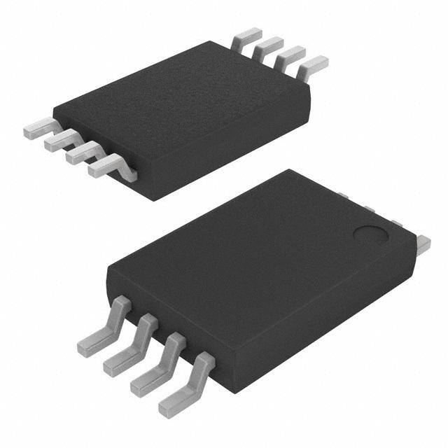
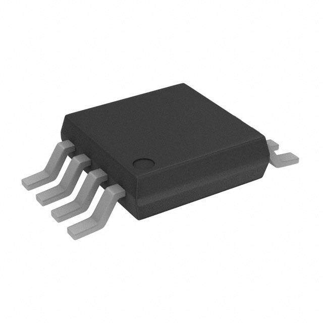
| 供应商器件封装 | 8-TSSOP |
| 共模抑制比—最小值 | 80 dB |
| 关闭 | No Shutdown |
| 其它名称 | 497-8065-6 |
| 其它有关文件 | http://www.st.com/web/catalog/sense_power/FM123/SC61/SS1378/PF65358?referrer=70071840http://www.st.com/web/catalog/sense_power/FM123/SC61/SS1614/PF65358?referrer=70071840 |
| 包装 | Digi-Reel® |
| 压摆率 | 16 V/µs |
| 双重电源电压 | +/- 5 V, +/- 9 V, +/- 12 V, +/- 15 V |
| 商标 | STMicroelectronics |
| 增益带宽生成 | 4 MHz |
| 增益带宽积 | 4MHz |
| 安装类型 | 表面贴装 |
| 安装风格 | SMD/SMT |
| 封装 | Reel |
| 封装/外壳 | 8-TSSOP(0.173",4.40mm 宽) |
| 封装/箱体 | TSSOP-8 |
| 工作温度 | -40°C ~ 105°C |
| 工作电源电压 | 6 V to 36 V, +/- 3 V to +/- 18 V |
| 工厂包装数量 | 4000 |
| 技术 | BiFET |
| 放大器类型 | J-FET |
| 最大双重电源电压 | +/- 18 V |
| 最大工作温度 | + 105 C |
| 最小双重电源电压 | +/- 3 V |
| 最小工作温度 | - 40 C |
| 标准包装 | 1 |
| 电压-电源,单/双 (±) | 6 V ~ 36 V, ±3 V ~ 18 V |
| 电压-输入失调 | 3mV |
| 电流-电源 | 1.4mA |
| 电流-输入偏置 | 20pA |
| 电流-输出/通道 | 40mA |
| 电源电流 | 2.5 mA |
| 电路数 | 2 |
| 系列 | TL082 |
| 转换速度 | 16 V/us |
| 输入偏压电流—最大 | 200 pA |
| 输入参考电压噪声 | 15 nV |
| 输入补偿电压 | 10 mV |
| 输出电流 | 40 mA |
| 输出类型 | - |
| 通道数量 | 2 Channel |


- 商务部:美国ITC正式对集成电路等产品启动337调查
- 曝三星4nm工艺存在良率问题 高通将骁龙8 Gen1或转产台积电
- 太阳诱电将投资9.5亿元在常州建新厂生产MLCC 预计2023年完工
- 英特尔发布欧洲新工厂建设计划 深化IDM 2.0 战略
- 台积电先进制程称霸业界 有大客户加持明年业绩稳了
- 达到5530亿美元!SIA预计今年全球半导体销售额将创下新高
- 英特尔拟将自动驾驶子公司Mobileye上市 估值或超500亿美元
- 三星加码芯片和SET,合并消费电子和移动部门,撤换高东真等 CEO
- 三星电子宣布重大人事变动 还合并消费电子和移动部门
- 海关总署:前11个月进口集成电路产品价值2.52万亿元 增长14.8%


PDF Datasheet 数据手册内容提取
TL082, TL082A, TL082B General purpose JFET dual operation amplifiers Datasheet - production data Description The TL082, TL082A and TL082B are high speed JFET input dual operational amplifiers incorporating well-matched, high voltage JFET and bipolar transistors in a monolithic integrated circuit. The devices feature high slew rates, low input bias and offset current, and low offset voltage temperature coefficient. Features Wide common-mode (up to V +) and CC differential voltage range Low input bias and offset current Output short-circuit protection High input impedance JFET input stage Internal frequency compensation Latch up free operation High slew rate: 16 V/µs (typical) June 2016 DocID2300 Rev 11 1/18 This is information on a product in full production. www.st.com
Contents TL082, TL082A, TL082B Contents 1 Schematic diagram .......................................................................... 3 2 Pin connections ............................................................................... 4 3 Absolute maximum ratings and operating conditions ................. 5 4 Electrical characteristics ................................................................ 6 5 Electrical characteristic curves ...................................................... 8 6 Parameter measurement information .......................................... 11 7 Typical applications ...................................................................... 12 8 Package information ..................................................................... 13 8.1 SO8 package information ................................................................ 14 8.2 TSSOP8 package information ......................................................... 15 9 Ordering information ..................................................................... 16 10 Revision history ............................................................................ 17 2/18 DocID2300 Rev 11
TL082, TL082A, TL082B Schematic diagram 1 Schematic diagram Figure 1: Schematic diagram DocID2300 Rev 11 3/18
Pin connections TL082, TL082A, TL082B 2 Pin connections Figure 2: Pin connections (top view) 4/18 DocID2300 Rev 11
TL082, TL082A, TL082B Absolute maximum ratings and operating conditions 3 Absolute maximum ratings and operating conditions Table 1: Absolute maximum ratings Symbol Parameter TL082I, AI, BI TL082C, AC, BC Unit VCC Supply voltage (1) ±18 Vin Input voltage (2) ±15 V Vid Differential input voltage (3) ±30 Ptot Power dissipation 680 mW Thermal resistance SO8 125 Rthja junction-to-ambient (4) TSSOP8 120 °C/W Thermal resistance SO8 40 Rthjc junction-to-case TSSOP8 37 Output short-circuit duration (5) Infinite Tstg Storage temperature range -65 to 150 °C HBM: human body model (6) 1 kV ESD MM: machine model (7) 200 V CDM: charged device model (8) 1500 Notes: (1)All voltage values, except differential voltage, are with respect to the zero reference level (ground) of the supply voltages where the zero reference level is the midpoint between VCC+ and VCC-. (2)The magnitude of the input voltage must never exceed the magnitude of the supply voltage or 15 volts, whichever is less. (3)Differential voltages are the non-inverting input terminal with respect to the inverting input terminal. (4)Short-circuits can cause excessive heating. Destructive dissipation can result from simultaneous short-circuit on all amplifiers. (5)The output may be shorted to ground or to either supply. Temperature and/or supply voltages must be limited to ensure that the dissipation rating is not exceeded (6)Human body model: 100 pF discharged through a 1.5 kΩ resistor between two pins of the device, done for all couples of pin combinations with other pins floating. (7)Machine model: a 200 pF cap is charged to the specified voltage, then discharged directly between two pins of the device with no external series resistor (internal resistor < 5 Ω), done for all couples of pin combinations with other pins floating. (8)Charged device model: all pins plus package are charged together to the specified voltage and then discharged directly to the ground. Table 2: Operating conditions Symbol Parameter TL082I, AI, BI TL082C, AC, BC Unit VCC Supply voltage 6 to 36 V Toper Operating free-air temperature range -40 to 105 0 to 70 °C DocID2300 Rev 11 5/18
Electrical characteristics TL082, TL082A, TL082B 4 Electrical characteristics Table 3: VCC = ±15V, Tamb = +25°C (unless otherwise specified) TL082I, AC, AI, BC, BI TL082C Symbol Parameter Unit Min. Typ. Max. Min. Typ. Max. Input offset voltage, Rs = 50 Ω, 3 10 3 10 Tamb = 25 °C, TL082 Input offset voltage, Rs = 50 Ω, 3 6 Tamb = 25 °C, TL082A Input offset voltage, Rs = 50 Ω, 1 3 Tamb = 25 °C, TL082B Vio mV Input offset voltage, Rs = 50 Ω, 13 13 Tmin ≤ Tamb ≤ Tmax, TL082 Input offset voltage, Rs = 50 Ω, 7 Tmin ≤ Tamb ≤ Tmax, TL082A Input offset voltage, Rs = 50 Ω, 5 Tmin ≤ Tamb ≤ Tmax, TL082B DVio Input offset voltage drift 10 10 µV/°C Input offset current, Tamb = 25 °C (1) 5 100 5 100 pA Iio Input offset current, Tmin ≤ Tamb ≤ Tmax (1) 4 10 nA Input bias current, Tamb = 25 °C 20 200 20 400 pA Iib Input bias current, Tmin ≤ Tamb ≤ Tmax 20 20 nA Large signal voltage gain, 50 200 25 200 RL = 2 kΩ, Vo = ±10 V, Tamb = 25 °C Avd V/mV Large signal voltage gain, 25 15 RL = 2 kΩ, Vo = ±10 V, Tmin ≤ Tamb ≤ Tmax Supply voltage rejection ratio, 80 86 70 86 RS = 50 Ω, Tamb = 25 °C SVR dB Supply voltage rejection ratio, 80 70 RS = 50 Ω, Tmin ≤ Tamb ≤ Tmax Supply current, no load, Tamb = 25 °C 1.4 2.5 1.4 2.5 ICC mA Supply current, no load, Tmin ≤ Tamb ≤ Tmax 2.5 2.5 15 15 Vicm Input common mode voltage range ±11 ±11 V -12 -12 Common mode rejection ratio, 80 86 70 86 RS = 50 Ω, Tamb = 25 °C CMR dB Common mode rejection ratio, 80 70 RS = 50 Ω, Tmin ≤ Tamb ≤ Tmax Output short-circuit current, 10 40 60 10 40 60 Tamb = 25 °C Ios mA Output short-circuit current, 10 60 10 60 Tmin ≤ Tamb ≤ Tmax 6/18 DocID2300 Rev 11
TL082, TL082A, TL082B Electrical characteristics TL082I, AC, AI, BC, BI TL082C Symbol Parameter Unit Min. Typ. Max. Min. Typ. Max. Output voltage swing, 10 12 10 12 Tamb = 25 °C, RL = 2 kΩ Output voltage swing, 12 13.5 12 13.5 Tamb = 25 °C, RL = 10 kΩ ±Vopp V Output voltage swing, 10 10 Tmin ≤ Tamb ≤ Tmax, RL = 2 kΩ Output voltage swing, 12 12 Tmin ≤ Tamb ≤ Tmax, RL = 10 kΩ SR Slew rate, Tamb = 25 °C, Vin = 10 V, 8 16 8 16 V/µs RL = 2 kΩ, CL = 100 pF, unity gain tr RRLis =e 2tim kΩe,, TCaLm b= =1 0205 p°CF,, uVnini t=y g2a0i nm V, 0.1 0.1 µs Kov ORLv e=r s2h koΩo,t ,C TLa m=b 1=0 205 p °FC, ,u Vniinty = g 2a0in m V, 10 10 % Gain bandwidth product, Tamb = 25 °C, GBP Vin = 10 mV, RL = 2 kΩ, CL = 100 pF, 2.5 4 2.5 4 MHz F = 100 kHz Ri Input resistance 1012 1012 Ω Total harmonic distortion, Tamb = 25 °C, THD F = 1 kHz, RL = 2 kΩ, CL = 100 pF, 0.01 0.01 % Av = 20 dB, Vo = 2 Vpp en EF q=u 1iv aklHezn t input noise voltage, RS = 100 Ω, 15 15 nV/√Hz ∅m Phase margin 45 45 degrees Vo1/Vo2 Channel separation, Av = 100 120 120 dB Notes: (1)The input bias currents are junction leakage currents which approximately double for every 10° C increase in the junction temperature. DocID2300 Rev 11 7/18
Electrical characteristic curves TL082, TL082A, TL082B 5 Electrical characteristic curves Figure 3: Maximum peak-to-peak output voltage versus Figure 4: Maximum peak-to-peak output voltage versus frequency frequency Figure 5: Maximum peak-to-peak output voltage versus Figure 6: Maximum peak-to-peak output voltage versus load resistance frequency Figure 7: Maximum peak-to-peak output voltage versus Figure 8: Maximum peak-to-peak output voltage versus free air temperature supply voltage 8/18 DocID2300 Rev 11
TL082, TL082A, TL082B Electrical characteristic curves Figure 9: Input bias current versus free air temperature Figure 10: Large signal differential voltage amplification and phase shift versus frequency Figure 11: Supply current per amplifier versus free air Figure 12: Large signal differential voltage amplification temperature versus free air temperature Figure 13: Total power dissipation versus free air Figure 14: Supply current per amplifier versus supply temperature voltage DocID2300 Rev 11 9/18
Electrical characteristic curves TL082, TL082A, TL082B Figure 15: Common-mode rejection ratio versus free air Figure 16: Output voltage versus elapsed time temperature Figure 17: Voltage follower large signal pulse response Figure 18: Equivalent input noise voltage versus frequency Figure 19: Total harmonic distortion versus frequency 10/18 DocID2300 Rev 11
TL082, TL082A, TL082B Parameter measurement information 6 Parameter measurement information Figure 20: Voltage follower Figure 21: Gain-of-10 inverting amplifier DocID2300 Rev 11 11/18
Typical applications TL082, TL082A, TL082B 7 Typical applications Figure 22: 100 kHz quadruple oscillator 1. These resistor values may be adjusted for a symmetrical output 12/18 DocID2300 Rev 11
TL082, TL082A, TL082B Package information 8 Package information In order to meet environmental requirements, ST offers these devices in different grades of ECOPACK® packages, depending on their level of environmental compliance. ECOPACK® specifications, grade definitions and product status are available at: www.st.com. ECOPACK® is an ST trademark. DocID2300 Rev 11 13/18
Package information TL082, TL082A, TL082B 8.1 SO8 package information Figure 23: SO8 package outline Table 4: SO8 mechanical data Dimensions Ref. Millimeters Inches Min. Typ. Max. Min. Typ. Max A 1.75 0.069 A1 0.10 0.25 0.004 0.010 A2 1.25 0.049 b 0.28 0.48 0.011 0.019 c 0.17 0.23 0.007 0.010 D 4.80 4.90 5.00 0.189 0.193 0.197 E 5.80 6.00 6.20 0.228 0.236 0.244 E1 3.80 3.90 4.00 0.150 0.154 0.157 e 1.27 0.050 h 0.25 0.50 0.010 0.020 L 0.40 1.27 0.016 0.050 L1 1.04 0.040 k 1° 8° 1° 8° ccc 0.10 0.004 14/18 DocID2300 Rev 11
TL082, TL082A, TL082B Package information 8.2 TSSOP8 package information Figure 24: TSSOP8 package outline Table 5: TSSOP8 mechanical data Dimensions Ref. Millimeters Inches Min. Typ. Max. Min. Typ. Max. A 1.2 0.047 A1 0.05 0.15 0.002 0.006 A2 0.80 1.00 1.05 0.031 0.039 0.041 b 0.19 0.30 0.007 0.012 c 0.09 0.20 0.004 0.008 D 2.90 3.00 3.10 0.114 0.118 0.122 E 6.20 6.40 6.60 0.244 0.252 0.260 E1 4.30 4.40 4.50 0.169 0.173 0.177 e 0.65 0.0256 k 0° 8° 0° 8° L 0.45 0.60 0.75 0.018 0.024 0.030 L1 1 0.039 aaa 0.1 0.004 DocID2300 Rev 11 15/18
Ordering information TL082, TL082A, TL082B 9 Ordering information Table 6: Order codes Order code Temperature range Package Packing Marking TL082ID SΟ8 Tube or tape and reel TL082IDT -40 °C to 105 °C 082I TL082IPT TSSOP8 Tape and reel TL082CD SΟ8 Tube or tape and reel TL082CDT 082C TL082CPT 0 °C to 70 °C TSSOP8 Tape and reel TL082ACDT 082AC SΟ8 TL082BCDT 082BC TL082IYDT (1) Tube or tape and reel 082IY TL082AIYDT (1) -40 °C to 105 °C SO8 (automotive grade) 82AIY TL082BIYDT (1) 82BIY Notes: (1)Qualified and characterized according to AEC Q100 and Q003 or equivalent, advanced screening according to AEC Q001 and Q 002 or equivalent. 16/18 DocID2300 Rev 11
TL082, TL082A, TL082B Revision history 10 Revision history Table 7: Document revision history Date Revision Changes 02-Apr-2001 1 Initial release. 2002-2003 2-7 Internal revisions. 30-Apr-2004 8 Format update. Added ESD information in Table 1 on page 4. Expanded order codes table and added automotive grade order codes. See Table 7 on page 16. 06-Mar-2007 9 Added Table 2: Operating conditions on page 4. Updated package information to make it compliant with the latest JEDEC standards. Removed information concerning military temperature range 12-Jun-2008 10 (TL082M*, TL082AM*, TL082BM*). Removed DIP8 package and all obsolete order codes Updated document layout 10-Jun-2016 11 Table 4: added L1 dimension Figure 24: removed silhouette and added package outline DocID2300 Rev 11 17/18
TL082, TL082A, TL082B IMPORTANT NOTICE – PLEASE READ CAREFULLY STMicroelectronics NV and its subsidiaries (“ST”) reserve the right to make changes, corrections, enhancements, modifications, and improvements to ST products and/or to this document at any time without notice. Purchasers should obtain the latest relevant information on ST products before placing orders. ST products are sold pursuant to ST’s terms and conditions of sale in place at the time of order acknowledgement. Purchasers are solely responsible for the choice, selection, and use of ST products and ST assumes no liability for application assistance or the design of Purchasers’ products. No license, express or implied, to any intellectual property right is granted by ST herein. Resale of ST products with provisions different from the information set forth herein shall void any warranty granted by ST for such product. ST and the ST logo are trademarks of ST. All other product or service names are the property of their respective owners. Information in this document supersedes and replaces information previously supplied in any prior versions of this document. © 2016 STMicroelectronics – All rights reserved 18/18 DocID2300 Rev 11
Mouser Electronics Authorized Distributor Click to View Pricing, Inventory, Delivery & Lifecycle Information: S TMicroelectronics: TL082ACD TL082ACN TL082IN TL082ID TL082CN TL082CD TL082IPT TL082CPT TL082IDT TL082CDT TL082ACDT TL082AIPT TL082BIYDT TL082BCDT TL082AIYDT TL082IYDT