ICGOO在线商城 > 集成电路(IC) > 数据采集 - 模数转换器 > TLC2543IDBRQ1

 Datasheet下载
- 型号: TLC2543IDBRQ1
- 制造商: Texas Instruments
- 库位|库存: xxxx|xxxx
- 要求:
| 数量阶梯 | 香港交货 | 国内含税 |
| +xxxx | $xxxx | ¥xxxx |
查看当月历史价格
查看今年历史价格
TLC2543IDBRQ1产品简介:
ICGOO电子元器件商城为您提供TLC2543IDBRQ1由Texas Instruments设计生产,在icgoo商城现货销售,并且可以通过原厂、代理商等渠道进行代购。 TLC2543IDBRQ1价格参考。Texas InstrumentsTLC2543IDBRQ1封装/规格:数据采集 - 模数转换器, 12 Bit Analog to Digital Converter 11 Input 1 SAR 20-SSOP。您可以下载TLC2543IDBRQ1参考资料、Datasheet数据手册功能说明书,资料中有TLC2543IDBRQ1 详细功能的应用电路图电压和使用方法及教程。
TLC2543IDBRQ1 是由 Texas Instruments 生产的一款 12 位、8 通道模数转换器(ADC)。它具有低功耗、高精度和多通道输入的特点,适用于多种数据采集应用场景。以下是该型号的一些典型应用场景:

 1. 工业自动化与控制
   TLC2543IDBRQ1 可用于工业自动化系统中,作为传感器信号的采集模块。例如,在温度、压力、湿度等环境参数的监测中,它可以将模拟信号转换为数字信号,供控制系统进一步处理。其多通道特性允许同时监控多个传感器,适合复杂的工业环境。

 2. 医疗设备
   在医疗设备中,如心电图机(ECG)、血压计、血糖仪等,TLC2543IDBRQ1 可以用于采集生理信号。由于其高精度和低噪声特性,能够确保采集到的信号准确无误,进而提高诊断的准确性。此外,它的低功耗设计也有助于延长便携式医疗设备的电池寿命。

 3. 智能家居与物联网
   TLC2543IDBRQ1 可用于智能家居系统中的环境监测,如空气质量检测、温湿度监控等。通过将传感器采集到的模拟信号转换为数字信号,再传输给中央控制器或云端平台进行分析,实现智能化管理和远程监控。

 4. 汽车电子
   在汽车电子系统中,TLC2543IDBRQ1 可用于车内的各种传感器信号采集,如发动机温度、油压、胎压等。这些数据对于车辆的安全性和性能优化至关重要。其多通道功能可以减少硬件冗余,降低系统复杂度。

 5. 音频处理
   该 ADC 还可用于音频设备中,如麦克风阵列、音响系统等。它能够将模拟音频信号转换为数字信号,便于后续的数字信号处理(DSP)操作,如降噪、音效增强等。

 6. 科学仪器
   在实验室环境中,TLC2543IDBRQ1 可用于精密测量仪器,如示波器、频谱分析仪等。其高分辨率和线性度使得它能够精确地捕捉微弱信号,满足科研需求。

总之,TLC2543IDBRQ1 凭借其多通道、高精度和低功耗的特点,广泛应用于工业、医疗、消费电子等多个领域,特别适合需要高精度模拟信号采集的应用场景。
| 参数 | 数值 |
| 产品目录 | 集成电路 (IC) |
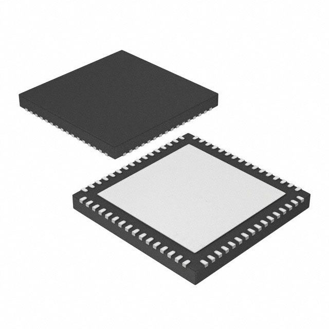
| 描述 | IC ADC 12BIT 11CH SW-CAP 20SSOP |
| 产品分类 | |
| 品牌 | Texas Instruments |
| 数据手册 | |
| 产品图片 |
|
| 产品型号 | TLC2543IDBRQ1 |
| rohs | 无铅 / 符合限制有害物质指令(RoHS)规范要求 |
| 产品系列 | 自动,AEC-Q100 |
| 产品培训模块 | http://www.digikey.cn/PTM/IndividualPTM.page?site=cn&lang=zhs&ptm=13240 |
| 位数 | 12 |
| 供应商器件封装 | 20-SSOP |
| 其它名称 | 296-29487-1 |
| 制造商产品页 | http://www.ti.com/general/docs/suppproductinfo.tsp?distId=10&orderablePartNumber=TLC2543IDBRQ1 |
| 包装 | 剪切带 (CT) |
| 安装类型 | 表面贴装 |
| 封装/外壳 | 20-SSOP(0.209",5.30mm 宽) |
| 工作温度 | -40°C ~ 85°C |
| 数据接口 | 串行 |
| 标准包装 | 1 |
| 特性 | - |
| 电压源 | 单电源 |
| 转换器数 | 1 |
| 输入数和类型 | 11 个单端,单极11 个单端,双极 |
| 采样率(每秒) | 66k |


- 商务部:美国ITC正式对集成电路等产品启动337调查
- 曝三星4nm工艺存在良率问题 高通将骁龙8 Gen1或转产台积电
- 太阳诱电将投资9.5亿元在常州建新厂生产MLCC 预计2023年完工
- 英特尔发布欧洲新工厂建设计划 深化IDM 2.0 战略
- 台积电先进制程称霸业界 有大客户加持明年业绩稳了
- 达到5530亿美元!SIA预计今年全球半导体销售额将创下新高
- 英特尔拟将自动驾驶子公司Mobileye上市 估值或超500亿美元
- 三星加码芯片和SET,合并消费电子和移动部门,撤换高东真等 CEO
- 三星电子宣布重大人事变动 还合并消费电子和移动部门
- 海关总署:前11个月进口集成电路产品价值2.52万亿元 增长14.8%


PDF Datasheet 数据手册内容提取
(cid:26) (cid:1)(cid:2)(cid:3)(cid:4)(cid:5)(cid:6)(cid:7)(cid:8)(cid:9)(cid:10) (cid:10)(cid:4)(cid:8)(cid:11)(cid:12)(cid:1) (cid:13)(cid:14)(cid:13)(cid:2)(cid:15)(cid:16)(cid:8)(cid:1)(cid:15)(cid:8)(cid:17)(cid:12)(cid:16)(cid:12)(cid:1)(cid:13)(cid:2) (cid:3)(cid:15)(cid:14)(cid:18)(cid:19)(cid:20)(cid:1)(cid:19)(cid:20)(cid:21) (cid:22)(cid:12)(cid:1)(cid:23) (cid:21)(cid:19)(cid:20)(cid:12)(cid:13)(cid:2) (cid:3)(cid:15)(cid:14)(cid:1)(cid:20)(cid:15)(cid:2) (cid:13)(cid:14)(cid:17) (cid:10)(cid:10) (cid:13)(cid:14)(cid:13)(cid:2)(cid:15)(cid:16) (cid:12)(cid:14)(cid:24)(cid:25)(cid:1)(cid:21) SGLS218D − NOVEMBER 2003 − REVISED MAY 2008 (cid:1) Qualified for Automotive Applications DB OR DW PACKAGE (cid:1) (TOP VIEW) 12-Bit Resolution A/D Converter (cid:1) 10-µs Conversion Time Over Operating AIN0 1 20 VCC Temperature AIN1 2 19 EOC (cid:1) 11 Analog Input Channels AIN2 3 18 I/O CLOCK (cid:1) Three Built-In Self-Test Modes AIN3 4 17 DATA INPUT (cid:1) Inherent Sample-and-Hold Function AIN4 5 16 DATA OUT (cid:1) Linearity Error...±1 LSB Max AIN5 6 15 CS AIN6 7 14 REF+ (cid:1) On-Chip System Clock AIN7 8 13 REF− (cid:1) End-of-Conversion Output AIN8 9 12 AIN10 (cid:1) Unipolar or Bipolar Output Operation GND 10 11 AIN9 (Signed Binary With Respect to 1/2 the Applied Voltage Reference) (cid:1) Programmable MSB or LSB First (cid:1) Programmable Power Down (cid:1) Programmable Output Data Length (cid:1) CMOS Technology (cid:1) Application Report Available‡ description The TLC2543 is a 12-bit, switched-capacitor, successive-approximation, analog-to-digital converters. Each device, with three control inputs [chip select (CS), the input-output clock, and the address input (DATA INPUT)], is designed for communication with the serial port of a host processor or peripheral through a serial 3-state output. The device allows high-speed data transfers from the host. In addition to the high-speed converter and versatile control capability, the device has an on-chip 14-channel multiplexer that can select any one of 11 inputs or any one of three internal self-test voltages. The sample-and-hold function is automatic. At the end of conversion, the end-of-conversion (EOC) output goes high to indicate that conversion is complete. The converter incorporated in the device features differential high-impedance reference inputs that facilitate ratiometric conversion, scaling, and isolation of analog circuitry from logic and supply noise. A switched-capacitor design allows low-error conversion over the full operating temperature range. (cid:1) ORDERING INFORMATION (cid:2) ORDERABLE TOP-SIDE TA PACKAGE PART NUMBER MARKING −40°C to 85°C SSOP − DB Tape and reel TLC2543IDBRQ1 TLC2543Q1 −40°C to 125°C SOP − DW Tape and reel TLC2543QDWRQ1 TLC2543Q1 †For the most current package and ordering information, see the Package Option Addendum at the end of this document, or see the TI web site at http://www.ti.com. ‡Package drawings, thermal data, and symbolization are available at http://www.ti.com/packaging. Please be aware that an important notice concerning availability, standard warranty, and use in critical applications of TexasInstruments semiconductor products and disclaimers thereto appears at the end of this data sheet. ‡Microcontroller Based Data Acquisition Using the TLC2543 12-bit Serial-Out ADC (SLAA012) (cid:24)(cid:20)(cid:15)(cid:17)(cid:25)(cid:3)(cid:1)(cid:12)(cid:15)(cid:14) (cid:17)(cid:13)(cid:1)(cid:13) (cid:27)(cid:28)(cid:29)(cid:30)(cid:31)!"#(cid:27)(cid:30)(cid:28) (cid:27)$ %&(cid:31)(cid:31)’(cid:28)# "$ (cid:30)(cid:29) (&)*(cid:27)%"#(cid:27)(cid:30)(cid:28) +"#’, Copyright 2008 Texas Instruments Incorporated (cid:24)(cid:31)(cid:30)+&%#$ %(cid:30)(cid:28)(cid:29)(cid:30)(cid:31)! #(cid:30) $(’%(cid:27)(cid:29)(cid:27)%"#(cid:27)(cid:30)(cid:28)$ (’(cid:31) #-’ #’(cid:31)!$ (cid:30)(cid:29) (cid:1)’."$ (cid:12)(cid:28)$#(cid:31)&!’(cid:28)#$ $#"(cid:28)+"(cid:31)+ /"(cid:31)(cid:31)"(cid:28)#0, (cid:24)(cid:31)(cid:30)+&%#(cid:27)(cid:30)(cid:28) ((cid:31)(cid:30)%’$$(cid:27)(cid:28)1 +(cid:30)’$ (cid:28)(cid:30)# (cid:28)’%’$$"(cid:31)(cid:27)*0 (cid:27)(cid:28)%*&+’ #’$#(cid:27)(cid:28)1 (cid:30)(cid:29) "** ("(cid:31)"!’#’(cid:31)$, POST OFFICE BOX 655303 • DALLAS, TEXAS 75265 1
(cid:1)(cid:2)(cid:3)(cid:4)(cid:5)(cid:6)(cid:7)(cid:8)(cid:9)(cid:10) (cid:26) (cid:10)(cid:4)(cid:8)(cid:11)(cid:12)(cid:1) (cid:13)(cid:14)(cid:13)(cid:2)(cid:15)(cid:16)(cid:8)(cid:1)(cid:15)(cid:8)(cid:17)(cid:12)(cid:16)(cid:12)(cid:1)(cid:13)(cid:2) (cid:3)(cid:15)(cid:14)(cid:18)(cid:19)(cid:20)(cid:1)(cid:19)(cid:20)(cid:21) (cid:22)(cid:12)(cid:1)(cid:23) (cid:21)(cid:19)(cid:20)(cid:12)(cid:13)(cid:2) (cid:3)(cid:15)(cid:14)(cid:1)(cid:20)(cid:15)(cid:2) (cid:13)(cid:14)(cid:17) (cid:10)(cid:10) (cid:13)(cid:14)(cid:13)(cid:2)(cid:15)(cid:16) (cid:12)(cid:14)(cid:24)(cid:25)(cid:1)(cid:21) SGLS218D − NOVEMBER 2003 − REVISED MAY 2008 functional block diagram REF+ REF− 14 13 AIN0 1 Sample-and- Analo1g2-t-oB-iDtigital 2 Hold AIN1 Converter 3 Function AIN2 (Switched Capacitors) 4 AIN3 5 AIN4 AIN5 6 14-Channel 12 7 Analog AIN6 Multiplexer 8 AIN7 AIN8 9 ODuatptaut 12 S1e2l-etoc-t1o rD aantad 16 DATA AIN9 11 4 Register Driver OUT 12 Input Address AIN10 Register 4 3 Control Logic Self-Test and I/O Reference Counters 19 EOC DATA 17 INPUT 18 I/O CLOCK 15 CS 2 POST OFFICE BOX 655303 • DALLAS, TEXAS 75265
(cid:26) (cid:1)(cid:2)(cid:3)(cid:4)(cid:5)(cid:6)(cid:7)(cid:8)(cid:9)(cid:10) (cid:10)(cid:4)(cid:8)(cid:11)(cid:12)(cid:1) (cid:13)(cid:14)(cid:13)(cid:2)(cid:15)(cid:16)(cid:8)(cid:1)(cid:15)(cid:8)(cid:17)(cid:12)(cid:16)(cid:12)(cid:1)(cid:13)(cid:2) (cid:3)(cid:15)(cid:14)(cid:18)(cid:19)(cid:20)(cid:1)(cid:19)(cid:20)(cid:21) (cid:22)(cid:12)(cid:1)(cid:23) (cid:21)(cid:19)(cid:20)(cid:12)(cid:13)(cid:2) (cid:3)(cid:15)(cid:14)(cid:1)(cid:20)(cid:15)(cid:2) (cid:13)(cid:14)(cid:17) (cid:10)(cid:10) (cid:13)(cid:14)(cid:13)(cid:2)(cid:15)(cid:16) (cid:12)(cid:14)(cid:24)(cid:25)(cid:1)(cid:21) SGLS218D − NOVEMBER 2003 − REVISED MAY 2008 Terminal Functions TERMINAL II//OO DDEESSCCRRIIPPTTIIOONN NAME NO. AIN0 − AIN10 1−9, I Analog input. These 11 analog-signal inputs are internally multiplexed. The driving source impedance should 11, 12 be less than or equal to 50 Ω for 4.1-MHz I/O CLOCK operation and be capable of slewing the analog input voltage into a capacitance of 60 pF. CS 15 I Chip select. A high-to-low transition on CS resets the internal counters and controls and enables DATA OUT, DATA INPUT, and I/O CLOCK. A low-to-high transition disables DATA INPUT and I/O CLOCK within a setup time. DATA INPUT 17 I Serial-data input. A 4-bit serial address selects the desired analog input or test voltage to be converted next. The serial data is presented with the MSB first and is shifted in on the first four rising edges of I/O CLOCK. After the four address bits are read into the address register, I/O CLOCK clocks the remaining bits in order. DATA OUT 16 O The 3-state serial output for the A/D conversion result. DATA OUT is in the high-impedance state when CS is high and active when CS is low. With a valid CS, DATA OUT is removed from the high-impedance state and is driven to the logic level corresponding to the MSB/LSB† value of the previous conversion result. The next falling edge of I/O CLOCK drives DATA OUT to the logic level corresponding to the next MSB/LSB, and the remaining bits are shifted out in order. EOC 19 O End of conversion. EOC goes from a high to a low logic level after the falling edge of the last I/O CLOCK and remains low until the conversion is complete and the data is ready for transfer. GND 10 Ground. GND is the ground return terminal for the internal circuitry. Unless otherwise noted, all voltage measurements are with respect to GND. I/O CLOCK 18 I Input/output clock. I/O CLOCK receives the serial input and performs the following four functions: 1. It clocks the eight input data bits into the input data register on the first eight rising edges of I/O CLOCK with the multiplexer address available after the fourth rising edge. 2. On the fourth falling edge of I/O CLOCK, the analog input voltage on the selected multiplexer input begins charging the capacitor array and continues to do so until the last falling edge of the I/O CLOCK. 3. It shifts the 11 remaining bits of the previous conversion data out on DATA OUT. Data changes on the falling edge of I/O CLOCK. 4. It transfers control of the conversion to the internal state controller on the falling edge of the last I/O CLOCK. REF+ 14 I Positive reference voltage The upper reference voltage value (nominally VCC) is applied to REF+. The maximum input voltage range is determined by the difference between the voltage applied to this terminal and the voltage applied to the REF− terminal. REF− 13 I Negative reference voltage. The lower reference voltage value (nominally ground) is applied to REF−. VCC 20 Positive supply voltage †MSB/LSB = Most significant bit / least significant bit POST OFFICE BOX 655303 • DALLAS, TEXAS 75265 3
(cid:1)(cid:2)(cid:3)(cid:4)(cid:5)(cid:6)(cid:7)(cid:8)(cid:9)(cid:10) (cid:26) (cid:10)(cid:4)(cid:8)(cid:11)(cid:12)(cid:1) (cid:13)(cid:14)(cid:13)(cid:2)(cid:15)(cid:16)(cid:8)(cid:1)(cid:15)(cid:8)(cid:17)(cid:12)(cid:16)(cid:12)(cid:1)(cid:13)(cid:2) (cid:3)(cid:15)(cid:14)(cid:18)(cid:19)(cid:20)(cid:1)(cid:19)(cid:20)(cid:21) (cid:22)(cid:12)(cid:1)(cid:23) (cid:21)(cid:19)(cid:20)(cid:12)(cid:13)(cid:2) (cid:3)(cid:15)(cid:14)(cid:1)(cid:20)(cid:15)(cid:2) (cid:13)(cid:14)(cid:17) (cid:10)(cid:10) (cid:13)(cid:14)(cid:13)(cid:2)(cid:15)(cid:16) (cid:12)(cid:14)(cid:24)(cid:25)(cid:1)(cid:21) SGLS218D − NOVEMBER 2003 − REVISED MAY 2008 absolute maximum ratings over operating free-air temperature range (unless otherwise noted)† Supply voltage range, V (see Note 1) . . . . . . . . . . . . . . . . . . . . . . . . . . . . . . . . . . . . . . . . . . . . . −0.5 V to 6.5 V CC Input voltage range, V (any input) . . . . . . . . . . . . . . . . . . . . . . . . . . . . . . . . . . . . . . . . . . . . −0.3 V to V + 0.3 V I CC Output voltage range, V . . . . . . . . . . . . . . . . . . . . . . . . . . . . . . . . . . . . . . . . . . . . . . . . . . . −0.3 V to V + 0.3 V O CC Positive reference voltage, V . . . . . . . . . . . . . . . . . . . . . . . . . . . . . . . . . . . . . . . . . . . . . . . . . . . . . . V + 0.1 V ref+ CC Negative reference voltage, V . . . . . . . . . . . . . . . . . . . . . . . . . . . . . . . . . . . . . . . . . . . . . . . . . . . . . . . . . . −0.1 V ref− Peak input current, I (any input) . . . . . . . . . . . . . . . . . . . . . . . . . . . . . . . . . . . . . . . . . . . . . . . . . . . . . . . . . . ±20 mA I Peak total input current, I (all inputs) . . . . . . . . . . . . . . . . . . . . . . . . . . . . . . . . . . . . . . . . . . . . . . . . . . . . . . ±30 mA I Operating free-air temperature range, T : I suffix . . . . . . . . . . . . . . . . . . . . . . . . . . . . . . . . . . . . . −40°C to 85°C A Q suffix . . . . . . . . . . . . . . . . . . . . . . . . . . . . . . . . . . . −40°C to 125°C Storage temperature range, T . . . . . . . . . . . . . . . . . . . . . . . . . . . . . . . . . . . . . . . . . . . . . . . . . . . −65°C to 150°C stg Lead temperature 1,6 mm (1/16 inch) from the case for 10 seconds . . . . . . . . . . . . . . . . . . . . . . . . . . . . 260°C †Stresses beyond those listed under “absolute maximum ratings” may cause permanent damage to the device. These are stress ratings only, and functional operation of the device at these or any other conditions beyond those indicated under “recommended operating conditions” is not implied. Exposure to absolute-maximum-rated conditions for extended periods may affect device reliability. NOTE 1: All voltage values are with respect to the GND terminal with REF− and GND wired together (unless otherwise noted). recommended operating conditions MIN NOM MAX UNIT Supply voltage, VCC 4.5 5 5.5 V Positive reference voltage, Vref+ (see Note 2) VCC V Negative reference voltage, Vref− (see Note 2) 0 V Differential reference voltage, Vref+ − Vref− (see Note 2) 2.5 VCC VCC+0.1 V Analog input voltage (see Note 2) 0 VCC V High-level control input voltage, VIH VCC = 4.5 V to 5.5 V 2 V Low-level control input voltage, VIL VCC = 4.5 V to 5.5 V 0.8 V Clock frequency at I/O CLOCK 0 4.1 MHz Setup time, address bits at DATA INPUT before I/O CLOCK↑, tsu(A) (see Figure 4) 100 ns Hold time, address bits after I/O CLOCK↑, th(A) (see Figure 4) 0 ns Hold time, CS low after last I/O CLOCK↓, th(CS) (see Figure 5) 0 ns Setup time, CS low before clocking in first address bit, tsu(CS) (see Note 3 and Figure 5) 1.425 µs Pulse duration, I/O CLOCK high, twH(I/O) 120 ns Pulse duration, I/O CLOCK low, twL(I/O) 120 ns Transition time, I/O CLOCK high to low, tt(I/O) (see Note 4 and Figure 6) 1 µs Transition time, DATA INPUT and CS, tt(CS) 10 µs I suffix −40 85 OOppeerraattiinngg ffrreeee--aaiirr tteemmppeerraattuurree,, TTAA °°CC Q suffix −40 125 NOTES: 2. Analog input voltages greater than that applied to REF+ convert as all ones (111111111111), while input voltages less than that applied to REF− convert as all zeros (000000000000). 3. To minimize errors caused by noise at the CS input, the internal circuitry waits for a setup time after CS↓ before responding to control input signals. No attempt should be made to clock in an address until the minimum CS setup time has elapsed. 4. This is the time required for the clock input signal to fall from VIHmin to VILmax or to rise from VILmax to VIHmin. In the vicinity of normal room temperature, the devices function with input clock transition time as slow as 1 µs for remote data acquisition applications where the sensor and the A/D converter are placed several feet away from the controlling microprocessor. 4 POST OFFICE BOX 655303 • DALLAS, TEXAS 75265
(cid:26) (cid:1)(cid:2)(cid:3)(cid:4)(cid:5)(cid:6)(cid:7)(cid:8)(cid:9)(cid:10) (cid:10)(cid:4)(cid:8)(cid:11)(cid:12)(cid:1) (cid:13)(cid:14)(cid:13)(cid:2)(cid:15)(cid:16)(cid:8)(cid:1)(cid:15)(cid:8)(cid:17)(cid:12)(cid:16)(cid:12)(cid:1)(cid:13)(cid:2) (cid:3)(cid:15)(cid:14)(cid:18)(cid:19)(cid:20)(cid:1)(cid:19)(cid:20)(cid:21) (cid:22)(cid:12)(cid:1)(cid:23) (cid:21)(cid:19)(cid:20)(cid:12)(cid:13)(cid:2) (cid:3)(cid:15)(cid:14)(cid:1)(cid:20)(cid:15)(cid:2) (cid:13)(cid:14)(cid:17) (cid:10)(cid:10) (cid:13)(cid:14)(cid:13)(cid:2)(cid:15)(cid:16) (cid:12)(cid:14)(cid:24)(cid:25)(cid:1)(cid:21) SGLS218D − NOVEMBER 2003 − REVISED MAY 2008 electrical characteristics over recommended operating free-air temperature range, VCC = Vref+ = 4.5 V to 5.5 V, f(I/O CLOCK) = 4.1 MHz (unless otherwise noted) PARAMETER TEST CONDITIONS MIN TYP† MAX UNIT VCC = 4.5 V, IOH = −1.6 mA 2.4 VVOOHH HHiigghh--lleevveell oouuttppuutt vvoollttaaggee VCC = 4.5 V to 5.5 V, IOH = −20 µA VCC−0.1 VV VCC = 4.5 V, IOL = 1.6 mA 0.4 VVOOLL LLooww--lleevveell oouuttppuutt vvoollttaaggee VCC = 4.5 V to 5.5 V, IOL = 20 µA 0.1 VV HHiigghh--iimmppeeddaannccee ooffff--ssttaattee oouuttppuutt VO = VCC, CS at VCC 1 2.5 IIOOZZ current VO = 0, CS at VCC 1 −2.5 µAA TA = −40°C to 85°C 0.5 1 IIIIHH HHiigghh--lleevveell iinnppuutt ccuurrrreenntt VVII == VVCCCC TA = 125°C 10 µAA TA = −40°C to 85°C 0.5 −1 IIIILL LLooww--lleevveell iinnppuutt ccuurrrreenntt VVII == 00 TA = 125°C −10 µAA ICC Operating supply current CS at 0 V 1 2.5 mA ICC(PD) Power-down current For all digital inputs, 0 ≤VI ≤ 0.5 V or VI ≥ VCC − 0.5 V 4 25 µA SSeelleecctteedd cchhaannnneell aatt VVCCCC,, TA = −40°C to 85°C 1 SSeelleecctteedd cchhaannnneell lleeaakkaaggee Unselected channel at 0 V TA = 125°C 10 µAA ccuurrrreenntt SSeelleecctteedd cchhaannnneell aatt 00 VV,, TA = −40°C to 85°C −1 Unselected channel at VCC TA = 125°C −10 Maximum static analog reference current into REF+ Vref+ = VCC, Vref− = GND 1 2.5 µA IInnppuutt Analog inputs 30 60 CCii ppFF capacitance Control inputs 5 15 †All typical values are at VCC = 5 V, TA = 25°C. POST OFFICE BOX 655303 • DALLAS, TEXAS 75265 5
(cid:1)(cid:2)(cid:3)(cid:4)(cid:5)(cid:6)(cid:7)(cid:8)(cid:9)(cid:10) (cid:26) (cid:10)(cid:4)(cid:8)(cid:11)(cid:12)(cid:1) (cid:13)(cid:14)(cid:13)(cid:2)(cid:15)(cid:16)(cid:8)(cid:1)(cid:15)(cid:8)(cid:17)(cid:12)(cid:16)(cid:12)(cid:1)(cid:13)(cid:2) (cid:3)(cid:15)(cid:14)(cid:18)(cid:19)(cid:20)(cid:1)(cid:19)(cid:20)(cid:21) (cid:22)(cid:12)(cid:1)(cid:23) (cid:21)(cid:19)(cid:20)(cid:12)(cid:13)(cid:2) (cid:3)(cid:15)(cid:14)(cid:1)(cid:20)(cid:15)(cid:2) (cid:13)(cid:14)(cid:17) (cid:10)(cid:10) (cid:13)(cid:14)(cid:13)(cid:2)(cid:15)(cid:16) (cid:12)(cid:14)(cid:24)(cid:25)(cid:1)(cid:21) SGLS218D − NOVEMBER 2003 − REVISED MAY 2008 operating characteristics over recommended operating free-air temperature range, VCC = Vref+ = 4.5 V to 5.5 V, f(I/O CLOCK) = 4.1 MHz PARAMETER TEST CONDITIONS MIN TYP† MAX UNIT EL Linearity error (see Note 5) See Figure 2 ±1 LSB ED Differential linearity error See Figure 2 ±1 LSB EO Offset error (see Note 6) SFiegeu rNeo 2te 2 and ±1.5 LSB EG Gain error (see Note 6) SFiegeu rNeo 2te 2 and ±1 LSB ET Total unadjusted error (see Note 7) ±1.75 LSB DATA INPUT = 1011 2048 SSeellff--tteesstt oouuttppuutt ccooddee ((sseeee TTaabbllee 33 aanndd NNoottee 88)) DATA INPUT = 1100 0 DATA INPUT = 1101 4095 t(conv) Conversion time SFiegeu rFei g1u4re 9− 8 10 µs 10 + total See Figure 9− I/O CLOCK tc Total cycle time (access, sample, and conversion) Figure 14 and Note 9 periods + µs td(I/O-EOC) I/O See Figures 9−14 tacq Channel acquisition time (sample) and Note 9 4 12 CLOCK periods tv Valid time, DATA OUT remains valid after I/O CLOCK↓ See Figure 6 10 ns td(I/O-DATA) Delay time, I/O CLOCK↓ to DATA OUT valid See Figure 6 150 ns td(I/O-EOC) Delay time, last I/O CLOCK↓ to EOC↓ See Figure 7 1.5 2.2 µs td(EOC-DATA) Delay time, EOC↑ to DATA OUT (MSB/LSB) See Figure 8 100 ns tPZH, tPZL Enable time, CS↓ to DATA OUT (MSB/LSB driven) See Figure 3 0.7 1.3 µs tPHZ, tPLZ Disable time, CS↑ to DATA OUT (high impedance) See Figure 3 70 150 ns tr(EOC) Rise time, EOC See Figure 8 15 50 ns tf(EOC) Fall time, EOC See Figure 7 15 50 ns tr(bus) Rise time, data bus See Figure 6 15 50 ns tf(bus) Fall time, data bus See Figure 6 15 50 ns Delay time, last I/O CLOCK↓ to CS↓ to abort conversion td(I/O-CS) (see Note 10) 5 µs †All typical values are at TA = 25°C. NOTES: 2. Analog input voltages greater than that applied to REF+ convert as all ones (111111111111), while input voltages less than that applied to REF− convert as all zeros (000000000000). 5. Linearity error is the maximum deviation from the best straight line through the A/D transfer characteristics. 6. Gain error is the difference between the actual midstep value and the nominal midstep value in the transfer diagram at the specified gain point after the offset error has been adjusted to zero. Offset error is the difference between the actual midstep value and the nominal midstep value at the offset point. 7. Total unadjusted error comprises linearity, zero-scale, and full-scale errors. 8. Both the input address and the output codes are expressed in positive logic. 9. I/O CLOCK period = 1/(I/O CLOCK frequency) (see Figure 7). 10. Any transitions of CS are recognized as valid only when the level is maintained for a setup time. CS must be taken low at ≤ 5 µs of the tenth I/O CLOCK falling edge to ensure a conversion is aborted. Between 5 µs and 10 µs, the result is uncertain as to whether the conversion is aborted or the conversion results are valid. 6 POST OFFICE BOX 655303 • DALLAS, TEXAS 75265
(cid:26) (cid:1)(cid:2)(cid:3)(cid:4)(cid:5)(cid:6)(cid:7)(cid:8)(cid:9)(cid:10) (cid:10)(cid:4)(cid:8)(cid:11)(cid:12)(cid:1) (cid:13)(cid:14)(cid:13)(cid:2)(cid:15)(cid:16)(cid:8)(cid:1)(cid:15)(cid:8)(cid:17)(cid:12)(cid:16)(cid:12)(cid:1)(cid:13)(cid:2) (cid:3)(cid:15)(cid:14)(cid:18)(cid:19)(cid:20)(cid:1)(cid:19)(cid:20)(cid:21) (cid:22)(cid:12)(cid:1)(cid:23) (cid:21)(cid:19)(cid:20)(cid:12)(cid:13)(cid:2) (cid:3)(cid:15)(cid:14)(cid:1)(cid:20)(cid:15)(cid:2) (cid:13)(cid:14)(cid:17) (cid:10)(cid:10) (cid:13)(cid:14)(cid:13)(cid:2)(cid:15)(cid:16) (cid:12)(cid:14)(cid:24)(cid:25)(cid:1)(cid:21) SGLS218D − NOVEMBER 2003 − REVISED MAY 2008 PARAMETER MEASUREMENT INFORMATION 15 V 50 Ω C1 C2 C3 10 µF 0.1 µF 470 pF TLC2543 _ 10 Ω U1 AIN0−AIN10 VI + C1 C2 C3 10 µF 0.1 µF 470 pF 50 Ω −15 V LOCATION DESCRIPTION PART NUMBER U1 OP27 — C1 10-µF 35-V tantalum capacitor — C2 0.1-µF ceramic NPO SMD capacitor AVX 12105C104KA105 or equivalent C3 470-pF porcelain Hi-Q SMD capacitor Johanson 201S420471JG4L or equivalent Figure 1. Analog Input Buffer to Analog Inputs AIN0−AIN10 Test Point VCC Test Point VCC RL = 2.18 kΩ RL = 2.18 kΩ EOC DATA OUT CL = 50 pF 12 kΩ CL = 100 pF 12 kΩ Figure 2. Load Circuits Data Valid 2 V 2 V CS 0.8 V DATA INPUT 0.8 V tPZH, tPZL tPHZ, tPLZ tsu(A) th(A) 2.4 V 90% DATA I/O CLOCK OUT 0.4 V 10% 0.8 V Figure 3. DATA OUT to Hi-Z Voltage Waveforms Figure 4. DATA INPUT and I/O CLOCK Voltage Waveforms POST OFFICE BOX 655303 • DALLAS, TEXAS 75265 7
(cid:1)(cid:2)(cid:3)(cid:4)(cid:5)(cid:6)(cid:7)(cid:8)(cid:9)(cid:10) (cid:26) (cid:10)(cid:4)(cid:8)(cid:11)(cid:12)(cid:1) (cid:13)(cid:14)(cid:13)(cid:2)(cid:15)(cid:16)(cid:8)(cid:1)(cid:15)(cid:8)(cid:17)(cid:12)(cid:16)(cid:12)(cid:1)(cid:13)(cid:2) (cid:3)(cid:15)(cid:14)(cid:18)(cid:19)(cid:20)(cid:1)(cid:19)(cid:20)(cid:21) (cid:22)(cid:12)(cid:1)(cid:23) (cid:21)(cid:19)(cid:20)(cid:12)(cid:13)(cid:2) (cid:3)(cid:15)(cid:14)(cid:1)(cid:20)(cid:15)(cid:2) (cid:13)(cid:14)(cid:17) (cid:10)(cid:10) (cid:13)(cid:14)(cid:13)(cid:2)(cid:15)(cid:16) (cid:12)(cid:14)(cid:24)(cid:25)(cid:1)(cid:21) SGLS218D − NOVEMBER 2003 − REVISED MAY 2008 PARAMETER MEASUREMENT INFORMATION 2 V CS 0.8 V tsu(CS) th(CS) I/O CLOCK Last 0.8 V 0.8 V Clock NOTE A: To ensure full conversion accuracy, it is recommended that no input signal change occurs while a conversion is ongoing. Figure 5. CS and I/O CLOCK Voltage Waveforms tt(I/O) tt(I/O) 2 V 2 V I/O CLOCK 0.8 V 0.8 V 0.8 V I/O CLOCK Period td(I/O-DATA) tv 2.4 V 2.4 V DATA OUT 0.4 V 0.4 V tr(bus), tf(bus) Figure 6. I/O CLOCK and DATA OUT Voltage Waveforms I/O CLOCK Last 0.8 V Clock td(I/O-EOC) EOC 2.4 V 0.4 V tf(EOC) Figure 7. I/O CLOCK and EOC Voltage Waveforms tr(EOC) EOC 2.4 V 0.4 V td(EOC-DATA) 2.4 V DATA OUT 0.4 V Valid MSB Figure 8. EOC and DATA OUT Voltage Waveforms 8 POST OFFICE BOX 655303 • DALLAS, TEXAS 75265
(cid:26) (cid:1)(cid:2)(cid:3)(cid:4)(cid:5)(cid:6)(cid:7)(cid:8)(cid:9)(cid:10) (cid:10)(cid:4)(cid:8)(cid:11)(cid:12)(cid:1) (cid:13)(cid:14)(cid:13)(cid:2)(cid:15)(cid:16)(cid:8)(cid:1)(cid:15)(cid:8)(cid:17)(cid:12)(cid:16)(cid:12)(cid:1)(cid:13)(cid:2) (cid:3)(cid:15)(cid:14)(cid:18)(cid:19)(cid:20)(cid:1)(cid:19)(cid:20)(cid:21) (cid:22)(cid:12)(cid:1)(cid:23) (cid:21)(cid:19)(cid:20)(cid:12)(cid:13)(cid:2) (cid:3)(cid:15)(cid:14)(cid:1)(cid:20)(cid:15)(cid:2) (cid:13)(cid:14)(cid:17) (cid:10)(cid:10) (cid:13)(cid:14)(cid:13)(cid:2)(cid:15)(cid:16) (cid:12)(cid:14)(cid:24)(cid:25)(cid:1)(cid:21) SGLS218D − NOVEMBER 2003 − REVISED MAY 2008 PARAMETER MEASUREMENT INFORMATION CS (see Note A) ÎÎÎÎÎÎÎ I/O 1 2 3 4 5 6 7 8 11 12 1 CLOCK ÎÎÎÎÎÎÎ Access Cycle B Sample Cycle B Hi-Z State DATA A11 A10 A9 A8 A7 A6 A5 A4 A1 A0 B11 OUT Previous Conversion Data MSB LSB ÎÎÎÎÎÎÎÎ Î ÎÎÎÎÎÎÎÎ ÎÎÎÎ DATA INPUTÎÎÎÎÎÎÎÎ Î ÎÎÎÎÎÎÎÎ ÎÎÎÎ B7 B6 B5 B4 B3 B2 B1 B0 C7 MSB LSB EOC Shift in New Multiplexer Address, t(conv) Simultaneously Shift Out Previous Conversion Value A/D Conversion Interval Initialize Initialize NOTE A: To minimize errors caused by noise at CS, the internal circuitry waits for a setup time after CS↓ before responding to control input signals. Therefore, no attempt should be made to clock in an address until the minimum CS setup time has elapsed. Figure 9. Timing for 12-Clock Transfer Using CS With MSB First CS (see Note A) I/O 1 2 3 4 5 6 7 8 11 12 1 CLOCK Access Cycle B Sample Cycle B DATA A11 A10 A9 A8 A7 A6 A5 A4 A1 A0 Low Level B11 OUT Previous Conversion Data ÎÎMÎSBÎÎÎÎÎÎÎÎÎÎÎÎÎÎÎÎ LSB ÎÎÎÎÎ DATAÎÎÎÎÎÎÎÎÎÎÎÎÎÎÎÎÎÎÎ ÎÎÎÎÎ INPUT ÎÎÎÎÎÎÎÎÎÎÎÎÎÎÎÎÎÎÎ ÎÎÎÎÎ B7 B6 B5 B4 B3 B2 B1 B0 C7 MSB LSB EOC Shift in New Multiplexer Address, t(conv) Simultaneously Shift Out Previous Conversion Value A/D Conversion Interval Initialize Initialize NOTE A: To minimize errors caused by noise at CS, the internal circuitry waits for a setup time after CS↓ before responding to control input signals. Therefore, no attempt should be made to clock in an address until the minimum CS setup time has elapsed. Figure 10. Timing for 12-Clock Transfer Not Using CS With MSB First POST OFFICE BOX 655303 • DALLAS, TEXAS 75265 9
(cid:1)(cid:2)(cid:3)(cid:4)(cid:5)(cid:6)(cid:7)(cid:8)(cid:9)(cid:10) (cid:26) (cid:10)(cid:4)(cid:8)(cid:11)(cid:12)(cid:1) (cid:13)(cid:14)(cid:13)(cid:2)(cid:15)(cid:16)(cid:8)(cid:1)(cid:15)(cid:8)(cid:17)(cid:12)(cid:16)(cid:12)(cid:1)(cid:13)(cid:2) (cid:3)(cid:15)(cid:14)(cid:18)(cid:19)(cid:20)(cid:1)(cid:19)(cid:20)(cid:21) (cid:22)(cid:12)(cid:1)(cid:23) (cid:21)(cid:19)(cid:20)(cid:12)(cid:13)(cid:2) (cid:3)(cid:15)(cid:14)(cid:1)(cid:20)(cid:15)(cid:2) (cid:13)(cid:14)(cid:17) (cid:10)(cid:10) (cid:13)(cid:14)(cid:13)(cid:2)(cid:15)(cid:16) (cid:12)(cid:14)(cid:24)(cid:25)(cid:1)(cid:21) SGLS218D − NOVEMBER 2003 − REVISED MAY 2008 PARAMETER MEASUREMENT INFORMATION CS (see Note A) ÎÎÎÎÎÎ I/O CLOCK 1 2 3 4 5 6 7 8 1 ÎÎÎÎÎÎ Access Cycle B Sample Cycle B Hi-Z DATA O UT A7 A6 A5 A4 A3 A2 A1 A0 B7 Previous Conversion Data MSB LSB ÎÎÎÎÎÎÎÎ Î ÎÎÎÎÎÎÎÎÎÎ ÎÎÎÎÎ DATA INPUT ÎÎÎÎÎÎÎÎ Î ÎÎÎÎÎÎÎÎÎÎ ÎÎÎÎÎ B7 B6 B5 B4 B3 B2 B1 B0 C7 MSB LSB EOC Shift in New Multiplexer Address, t(conv) Simultaneously Shift Out Previous Conversion Value A/D Conversion Interval Initialize Initialize NOTE A: To minimize errors caused by noise at CS, the internal circuitry waits for a setup time after CS↓ before responding to control input signals. Therefore, no attempt should be made to clock in an address until the minimum CS setup time has elapsed. Figure 11. Timing for 8-Clock Transfer Using CS With MSB First CS (see Note A) I/O CLOCK 1 2 3 4 5 6 7 8 1 Access Cycle B Sample Cycle B DATA OUT A7 A6 A5 A4 A3 A2 A1 A0 Low Level B7 Previous Conversion Data MSB LSB ÎÎÎÎÎÎ ÎÎÎÎÎÎÎÎÎÎÎ ÎÎÎÎ DATA INPUT ÎÎÎÎÎÎ ÎÎÎÎÎÎÎÎÎÎÎ ÎÎÎÎ B7 B6 B5 B4 B3 B2 B1 B0 C7 MSB LSB EOC Shift in New Multiplexer Address, t(conv) Simultaneously Shift Out Previous Conversion Value A/D Conversion Interval Initialize Initialize NOTE A: To minimize errors caused by noise at CS, the internal circuitry waits for a setup time after CS↓ before responding to control input signals. Therefore, no attempt should be made to clock in an address until the minimum CS setup time has elapsed. Figure 12. Timing for 8-Clock Transfer Not Using CS With MSB First 10 POST OFFICE BOX 655303 • DALLAS, TEXAS 75265
(cid:26) (cid:1)(cid:2)(cid:3)(cid:4)(cid:5)(cid:6)(cid:7)(cid:8)(cid:9)(cid:10) (cid:10)(cid:4)(cid:8)(cid:11)(cid:12)(cid:1) (cid:13)(cid:14)(cid:13)(cid:2)(cid:15)(cid:16)(cid:8)(cid:1)(cid:15)(cid:8)(cid:17)(cid:12)(cid:16)(cid:12)(cid:1)(cid:13)(cid:2) (cid:3)(cid:15)(cid:14)(cid:18)(cid:19)(cid:20)(cid:1)(cid:19)(cid:20)(cid:21) (cid:22)(cid:12)(cid:1)(cid:23) (cid:21)(cid:19)(cid:20)(cid:12)(cid:13)(cid:2) (cid:3)(cid:15)(cid:14)(cid:1)(cid:20)(cid:15)(cid:2) (cid:13)(cid:14)(cid:17) (cid:10)(cid:10) (cid:13)(cid:14)(cid:13)(cid:2)(cid:15)(cid:16) (cid:12)(cid:14)(cid:24)(cid:25)(cid:1)(cid:21) SGLS218D − NOVEMBER 2003 − REVISED MAY 2008 PARAMETER MEASUREMENT INFORMATION CS (see Note A) ÎÎÎÎÎÎÎ I/O 1 2 3 4 5 6 7 8 15 16 1 CLOCK ÎÎÎÎÎÎÎ Access Cycle B Sample Cycle B Hi-Z State DATA A15 A14 A13 A12 A11 A10 A9 A8 A1 A0 B15 OUT Previous Conversion Data MSB LSB ÎÎÎÎÎÎÎÎÎÎÎÎÎÎÎÎÎÎÎÎ ÎÎ DATAÎÎÎÎÎÎÎÎÎÎÎÎÎÎÎÎÎÎÎÎ ÎÎÎ INPUT B7 B6 B5 B4 B3 B2 B1 B0 C7 MSB LSB EOC Shift in New Multiplexer Address, t(conv) Simultaneously Shift Out Previous Conversion Value A/D Conversion Interval Initialize Initialize NOTE A: To minimize errors caused by noise at CS, the internal circuitry waits for a setup time after CS↓ before responding to control input signals. Therefore, no attempt should be made to clock in an address until the minimum CS setup time has elapsed. Figure 13. Timing for 16-Clock Transfer Using CS With MSB First CS (see Note A) I/O 1 2 3 4 5 6 7 8 15 16 1 CLOCK Access Cycle B Sample Cycle B DATA A15 A14 A13 A12 A11 A10 A9 A8 A1 A0 Low Level B15 OUT Previous Conversion Data ÎÎMSB ÎÎÎÎÎÎÎÎÎÎÎÎÎÎÎ LSB ÎÎÎÎÎ DATA ÎÎ ÎÎÎÎÎÎÎÎÎÎÎÎÎÎÎ ÎÎÎÎÎ INPUT B7 B6 B5 B4 B3 B2 B1 B0 C7 MSB LSB EOC Shift in New Multiplexer Address, t(conv) Simultaneously Shift Out Previous Conversion Value A/D Conversion Interval Initialize NOTE A: To minimize errors caused by noise at CS, the internal circuitry waits for a setup time after CS↓ before responding to control input signals. Therefore, no attempt should be made to clock in an address until the minimum CS setup time has elapsed. Figure 14. Timing for 16-Clock Transfer Not Using CS With MSB First POST OFFICE BOX 655303 • DALLAS, TEXAS 75265 11
(cid:1)(cid:2)(cid:3)(cid:4)(cid:5)(cid:6)(cid:7)(cid:8)(cid:9)(cid:10) (cid:26) (cid:10)(cid:4)(cid:8)(cid:11)(cid:12)(cid:1) (cid:13)(cid:14)(cid:13)(cid:2)(cid:15)(cid:16)(cid:8)(cid:1)(cid:15)(cid:8)(cid:17)(cid:12)(cid:16)(cid:12)(cid:1)(cid:13)(cid:2) (cid:3)(cid:15)(cid:14)(cid:18)(cid:19)(cid:20)(cid:1)(cid:19)(cid:20)(cid:21) (cid:22)(cid:12)(cid:1)(cid:23) (cid:21)(cid:19)(cid:20)(cid:12)(cid:13)(cid:2) (cid:3)(cid:15)(cid:14)(cid:1)(cid:20)(cid:15)(cid:2) (cid:13)(cid:14)(cid:17) (cid:10)(cid:10) (cid:13)(cid:14)(cid:13)(cid:2)(cid:15)(cid:16) (cid:12)(cid:14)(cid:24)(cid:25)(cid:1)(cid:21) SGLS218D − NOVEMBER 2003 − REVISED MAY 2008 PRINCIPLES OF OPERATION Initially, with chip select (CS) high, I/O CLOCK and DATA INPUT are disabled and DATA OUT is in the high-impedance state. CS going low begins the conversion sequence by enabling I/O CLOCK and DATA INPUT and removes DATA OUT from the high-impedance state. The input data is an 8-bit data stream consisting of a 4-bit analog channel address (D7−D4), a 2-bit data length select (D3−D2), an output MSB or LSB first bit (D1), and a unipolar or bipolar output select bit (D0) that are applied to DATA INPUT. The I/O CLOCK sequence applied to the I/O CLOCK terminal transfers this data to the input data register. During this transfer, the I/O CLOCK sequence also shifts the previous conversion result from the output data register to DATA OUT. The I/O CLOCK receives the input sequence of 8, 12, or 16 clock cycles long depending on the data-length selection in the input data register. Sampling of the analog input begins on the fourth falling edge of the input I/O CLOCK sequence and is held after the last falling edge of the I/O CLOCK sequence. The last falling edge of the I/O CLOCK sequence also takes EOC low and begins the conversion. converter operation The operation of the converter is organized as a succession of two distinct cycles: 1) the I/O cycle and 2) the actual conversion cycle. I/O cycle The I/O cycle is defined by the externally provided I/O CLOCK and lasts 8, 12, or 16 clock periods, depending on the selected output data length. During the I/O cycle, the following two operations take place simultaneously. An 8-bit data stream consisting of address and control information is provided to DATA INPUT. This data is shifted into the device on the rising edge of the first eight I/O CLOCKs. DATA INPUT is ignored after the first eight clocks during 12- or 16-clock I/O transfers. The data output, with a length of 8, 12, or 16 bits, is provided serially on DATA OUT. When CS is held low, the first output data bit occurs on the rising edge of EOC. When CS is negated between conversions, the first output data bit occurs on the falling edge of CS. This data is the result of the previous conversion period, and after the first output data bit, each succeeding bit is clocked out on the falling edge of each succeeding I/O CLOCK. conversion cycle The conversion cycle is transparent to the user and it is controlled by an internal clock synchronized to I/O CLOCK. During the conversion period, the device performs a successive-approximation conversion on the analog input voltage. The EOC output goes low at the start of the conversion cycle and goes high when conversion is complete and the output data register is latched. A conversion cycle is started only after the I/O cycle is completed, which minimizes the influence of external digital noise on the accuracy of the conversion. 12 POST OFFICE BOX 655303 • DALLAS, TEXAS 75265
(cid:26) (cid:1)(cid:2)(cid:3)(cid:4)(cid:5)(cid:6)(cid:7)(cid:8)(cid:9)(cid:10) (cid:10)(cid:4)(cid:8)(cid:11)(cid:12)(cid:1) (cid:13)(cid:14)(cid:13)(cid:2)(cid:15)(cid:16)(cid:8)(cid:1)(cid:15)(cid:8)(cid:17)(cid:12)(cid:16)(cid:12)(cid:1)(cid:13)(cid:2) (cid:3)(cid:15)(cid:14)(cid:18)(cid:19)(cid:20)(cid:1)(cid:19)(cid:20)(cid:21) (cid:22)(cid:12)(cid:1)(cid:23) (cid:21)(cid:19)(cid:20)(cid:12)(cid:13)(cid:2) (cid:3)(cid:15)(cid:14)(cid:1)(cid:20)(cid:15)(cid:2) (cid:13)(cid:14)(cid:17) (cid:10)(cid:10) (cid:13)(cid:14)(cid:13)(cid:2)(cid:15)(cid:16) (cid:12)(cid:14)(cid:24)(cid:25)(cid:1)(cid:21) SGLS218D − NOVEMBER 2003 − REVISED MAY 2008 PRINCIPLES OF OPERATION power up and initialization After power up, CS must be taken from high to low to begin an I/O cycle. EOC is initially high, and the input data register is set to all zeroes. The contents of the output data register are random and the first conversion result should be ignored. To initialize during operation, CS is taken high and is then returned low to begin the next I/O cycle. The first conversion after the device has returned from the power-down state may not read accurately due to internal device settling. Table 1. Operational Terminology Current (N) I/O cycle The entire I/O CLOCK sequence that transfers address and control data into the data register and clocks the digital result from the previous conversion from DATA OUT. Current (N) conversion cycle The conversion cycle starts immediately after the current I/O cycle. The end of the current I/O cycle is the last clock falling edge in the I/O CLOCK sequence. The current conversion result is loaded into the output register when conversion is complete. Current (N) conversion result The current conversion result is serially shifted out on the next I/O cycle. Previous (N−1) conversion cycle The conversion cycle just prior to the current I/O cycle. Next (N+1) I/O cycle The I/O period that follows the current conversion cycle. Example: In the 12-bit mode, the result of the current conversion cycle is a 12-bit serial-data stream clocked out during the next I/O cycle. The current I/O cycle must be exactly 12 bits long to maintain synchronization, even when this corrupts the output data from the previous conversion. The current conversion is begun immediately after the twelfth falling edge of the current I/O cycle. POST OFFICE BOX 655303 • DALLAS, TEXAS 75265 13
(cid:1)(cid:2)(cid:3)(cid:4)(cid:5)(cid:6)(cid:7)(cid:8)(cid:9)(cid:10) (cid:26) (cid:10)(cid:4)(cid:8)(cid:11)(cid:12)(cid:1) (cid:13)(cid:14)(cid:13)(cid:2)(cid:15)(cid:16)(cid:8)(cid:1)(cid:15)(cid:8)(cid:17)(cid:12)(cid:16)(cid:12)(cid:1)(cid:13)(cid:2) (cid:3)(cid:15)(cid:14)(cid:18)(cid:19)(cid:20)(cid:1)(cid:19)(cid:20)(cid:21) (cid:22)(cid:12)(cid:1)(cid:23) (cid:21)(cid:19)(cid:20)(cid:12)(cid:13)(cid:2) (cid:3)(cid:15)(cid:14)(cid:1)(cid:20)(cid:15)(cid:2) (cid:13)(cid:14)(cid:17) (cid:10)(cid:10) (cid:13)(cid:14)(cid:13)(cid:2)(cid:15)(cid:16) (cid:12)(cid:14)(cid:24)(cid:25)(cid:1)(cid:21) SGLS218D − NOVEMBER 2003 − REVISED MAY 2008 PRINCIPLES OF OPERATION data input The data input is internally connected to an 8-bit serial-input address and control register. The register defines the operation of the converter and the output data length. The host provides the data word with the MSB first. Each data bit is clocked in on the rising edge of the I/O CLOCK sequence (see Table 2 for the data input-register format). Table 2. Input-Register Format INPUT DATA BYTE ADDRESS BITS L1 L0 LSBF BIP FFUUNNCCTTIIOONN SSEELLEECCTT D7 D6 D5 D4 D3 D2 D1 D0 (MSB) (LSB) Select input channel AIN0 0 0 0 0 AIN1 0 0 0 1 AIN2 0 0 1 0 AIN3 0 0 1 1 AIN4 0 1 0 0 AIN5 0 1 0 1 AIN6 0 1 1 0 AIN7 0 1 1 1 AIN8 1 0 0 0 AIN9 1 0 0 1 AIN10 1 0 1 0 Select test voltage (Vref+ − Vref−)/2 1 0 1 1 Vref− 1 1 0 0 Vref+ 1 1 0 1 Software power down 1 1 1 0 Output data length 8 bits 0 1 12 bits X† 0 16 bits 1 1 Output data format MSB first 0 LSB first (LSBF) 1 Unipolar (binary) 0 Bipolar (BIP) 2s complement 1 †X represents a do not care condition. data input address bits The four MSBs (D7 − D4) of the data register address one of the 11 input channels, a reference-test voltage, or the power-down mode. The address bits affect the current conversion, which is the conversion that immediately follows the current I/O cycle. The reference voltage is nominally equal to V − V . ref+ ref− 14 POST OFFICE BOX 655303 • DALLAS, TEXAS 75265
(cid:26) (cid:1)(cid:2)(cid:3)(cid:4)(cid:5)(cid:6)(cid:7)(cid:8)(cid:9)(cid:10) (cid:10)(cid:4)(cid:8)(cid:11)(cid:12)(cid:1) (cid:13)(cid:14)(cid:13)(cid:2)(cid:15)(cid:16)(cid:8)(cid:1)(cid:15)(cid:8)(cid:17)(cid:12)(cid:16)(cid:12)(cid:1)(cid:13)(cid:2) (cid:3)(cid:15)(cid:14)(cid:18)(cid:19)(cid:20)(cid:1)(cid:19)(cid:20)(cid:21) (cid:22)(cid:12)(cid:1)(cid:23) (cid:21)(cid:19)(cid:20)(cid:12)(cid:13)(cid:2) (cid:3)(cid:15)(cid:14)(cid:1)(cid:20)(cid:15)(cid:2) (cid:13)(cid:14)(cid:17) (cid:10)(cid:10) (cid:13)(cid:14)(cid:13)(cid:2)(cid:15)(cid:16) (cid:12)(cid:14)(cid:24)(cid:25)(cid:1)(cid:21) SGLS218D − NOVEMBER 2003 − REVISED MAY 2008 PRINCIPLES OF OPERATION data output length The next two bits (D3 and D2) of the data register select the output data length. The data-length selection is valid for the current I/O cycle (the cycle in which the data is read). The data-length selection, being valid for the current I/O cycle, allows device start-up without losing I/O synchronization. A data length of 8, 12, or 16 bits can be selected. Since the converter has 12-bit resolution, a data length of 12 bits is suggested. With D3 and D2 set to 00 or 10, the device is in the 12-bit data-length mode and the result of the current conversion is output as a 12-bit serial data stream during the next I/O cycle. The current I/O cycle must be exactly 12 bits long for proper synchronization, even when this means corrupting the output data from a previous conversion. The current conversion is started immediately after the twelfth falling edge of the current I/O cycle. With bits D3 and D2 set to 11, the 16-bit data-length mode is selected, which allows convenient communication with 16-bit serial interfaces. In the 16-bit mode, the result of the current conversion is output as a 16-bit serial data stream during the next I/O cycle with the four LSBs always reset to 0 (pad bits). The current I/O cycle must be exactly 16 bits long to maintain synchronization even when this means corrupting the output data from the previous conversion. The current conversion is started immediately after the sixteenth falling edge of the current I/O cycle. With bits D3 and D2 set to 01, the 8-bit data-length mode is selected, which allows fast communication with 8-bit serial interfaces. In the 8-bit mode, the result of the current conversion is output as an 8-bit serial data stream during the next I/O cycle. The current I/O cycle must be exactly eight bits long to maintain synchronization, even when this means corrupting the output data from the previous conversion. The four LSBs of the conversion result are truncated and discarded. The current conversion is started immediately after the eighth falling edge of the current I/O cycle. Since D3 and D2 take effect on the current I/O cycle when the data length is programmed, there can be a conflict with the previous cycle when the data-word length is changed from one cycle to the next. This may occur when the data format is selected to be least significant bit first, since at the time the data length change becomes effective (six rising edges of I/O CLOCK), the previous conversion result has already started shifting out. In actual operation, when different data lengths are required within an application and the data length is changed between two conversions, no more than one conversion result can be corrupted and only when it is shifted out in LSB-first format. sampling period During the sampling period, one of the analog inputs is internally connected to the capacitor array of the converter to store the analog input signal. The converter starts sampling the selected input immediately after the four address bits have been clocked into the input data register. Sampling starts on the fourth falling edge of I/O CLOCK. The converter remains in the sampling mode until the 8th, 12th, or 16th falling edge of the I/O CLOCK depending on the data-length selection. After the EOC delay time from the last I/O CLOCK falling edge, the EOC output goes low indicating that the sampling period is over and the conversion period has begun. After EOC goes low, the analog input can be changed without affecting the conversion result. Since the delay from the falling edge of the last I/O CLOCK to EOC low is fixed, time-varying analog input signals can be digitized at a fixed rate without introducing systematic harmonic distortion or noise due to timing uncertainty. After the 8-bit data stream has been clocked in, DATA INPUT should be held at a fixed digital level until EOC goes high (indicating that the conversion is complete) to maximize the sampling accuracy and minimize the influence of external digital noise. POST OFFICE BOX 655303 • DALLAS, TEXAS 75265 15
(cid:1)(cid:2)(cid:3)(cid:4)(cid:5)(cid:6)(cid:7)(cid:8)(cid:9)(cid:10) (cid:26) (cid:10)(cid:4)(cid:8)(cid:11)(cid:12)(cid:1) (cid:13)(cid:14)(cid:13)(cid:2)(cid:15)(cid:16)(cid:8)(cid:1)(cid:15)(cid:8)(cid:17)(cid:12)(cid:16)(cid:12)(cid:1)(cid:13)(cid:2) (cid:3)(cid:15)(cid:14)(cid:18)(cid:19)(cid:20)(cid:1)(cid:19)(cid:20)(cid:21) (cid:22)(cid:12)(cid:1)(cid:23) (cid:21)(cid:19)(cid:20)(cid:12)(cid:13)(cid:2) (cid:3)(cid:15)(cid:14)(cid:1)(cid:20)(cid:15)(cid:2) (cid:13)(cid:14)(cid:17) (cid:10)(cid:10) (cid:13)(cid:14)(cid:13)(cid:2)(cid:15)(cid:16) (cid:12)(cid:14)(cid:24)(cid:25)(cid:1)(cid:21) SGLS218D − NOVEMBER 2003 − REVISED MAY 2008 PRINCIPLES OF OPERATION data register, LSB first D1 in the input data register (LSB first) controls the direction of the output binary data transfer. When D1 is reset to 0, the conversion result is shifted out MSB first. When set to 1, the data is shifted out LSB first. Selection of MSB first or LSB first always affects the next I/O cycle and not the current I/O cycle. When changing from one data direction to another, the current I/O cycle is never disrupted. data register, bipolar format D0 (BIP) in the input data register controls the binary data format used to represent the conversion result. When D0 is cleared to 0, the conversion result is represented as unipolar (unsigned binary) data. Nominally, the conversion result of an input voltage equal to V is a code of all zeros (000...0), the conversion result of ref− an input voltage equal to Vref+ is a code of all ones (111...1), and the conversion result of (Vref(cid:1)+ + Vref−)/2 is a code of a one followed by zeros (100...0). When D0 is set to 1, the conversion result is represented as bipolar (signed binary) data. Nominally, conversion of an input voltage equal to V is a code of a one followed by zeros (100...0), conversion of an input voltage ref− equal to V is a code of a zero followed by all ones (011...1), and the conversion of (V + V )/2 is a ref+ ref+ ref− code of all zeros (000...0). The MSB is interpreted as the sign bit. The bipolar data format is related to the unipolar format in that the MSBs are always each other’s complement. Selection of the unipolar or bipolar format always affects the current conversion cycle, and the result is output during the next I/O cycle. When changing between unipolar and bipolar formats, the data output during the current I/O cycle is not affected. EOC output The EOC signal indicates the beginning and the end of conversion. In the reset state, EOC is always high. During the sampling period (beginning after the fourth falling edge of the I/O CLOCK sequence), EOC remains high until the internal sampling switch of the converter is safely opened. The opening of the sampling switch occurs after the 8th, 12th, or 16th I/O CLOCK falling edge, depending on the data-length selection in the input data register. After the EOC signal goes low, the analog input signal can be changed without affecting the conversion result. The EOC signal goes high again after the conversion is completed and the conversion result is latched into the output data register. The rising edge of EOC returns the converter to a reset state and a new I/O cycle begins. On the rising edge of EOC, the first bit of the current conversion result is on DATA OUT when CS is low. When CS is negated between conversions, the first bit of the current conversion result occurs at DATA OUT on the falling edge of CS. data format and pad bits D3 and D2 of the input data register determine the number of significant bits in the digital output that represent the conversion result. The LSB-first bit determines the direction of the data transfer, while the BIP bit determines the arithmetic conversion. The numerical data is always justified toward the MSB in any output format. The internal conversion result is always 12 bits long. When an 8-bit data transfer is selected, the four LSBs of the internal result are discarded to provide a faster one-byte transfer. When a 12-bit transfer is used, all bits are transferred. When a 16-bit transfer is used, four LSB pad bits are always appended to the internal conversion result. In the LSB-first mode, four leading zeros are output. In the MSB-first mode, the last four bits output are zeros. 16 POST OFFICE BOX 655303 • DALLAS, TEXAS 75265
(cid:26) (cid:1)(cid:2)(cid:3)(cid:4)(cid:5)(cid:6)(cid:7)(cid:8)(cid:9)(cid:10) (cid:10)(cid:4)(cid:8)(cid:11)(cid:12)(cid:1) (cid:13)(cid:14)(cid:13)(cid:2)(cid:15)(cid:16)(cid:8)(cid:1)(cid:15)(cid:8)(cid:17)(cid:12)(cid:16)(cid:12)(cid:1)(cid:13)(cid:2) (cid:3)(cid:15)(cid:14)(cid:18)(cid:19)(cid:20)(cid:1)(cid:19)(cid:20)(cid:21) (cid:22)(cid:12)(cid:1)(cid:23) (cid:21)(cid:19)(cid:20)(cid:12)(cid:13)(cid:2) (cid:3)(cid:15)(cid:14)(cid:1)(cid:20)(cid:15)(cid:2) (cid:13)(cid:14)(cid:17) (cid:10)(cid:10) (cid:13)(cid:14)(cid:13)(cid:2)(cid:15)(cid:16) (cid:12)(cid:14)(cid:24)(cid:25)(cid:1)(cid:21) SGLS218D − NOVEMBER 2003 − REVISED MAY 2008 PRINCIPLES OF OPERATION data format and pad bits (continued) When CS is held low continuously, the first data bit of the newly completed conversion occurs on DATA OUT on the rising edge of EOC. When a new conversion is started after the last falling edge of I/O CLOCK, EOC goes low and the serial output is forced to a setting of 0 until EOC goes high again. When CS is negated between conversions, the first data bit occurs on DATA OUT on the falling edge of CS. On each subsequent falling edge of I/O CLOCK after the first data bit appears, the data is changed to the next bit in the serial conversion result until the required number of bits has been output. chip-select input (CS) CS enables and disables the device. During normal operation, CS should be low. Although the use of CS is not necessary to synchronize a data transfer, it can be brought high between conversions to coordinate the data transfer of several devices sharing the same bus. When CS is brought high, the serial-data output is immediately brought to the high-impedance state, releasing its output data line to other devices that may share it. After an internally generated debounce time, I/O CLOCK is inhibited, thus preventing any further change in the internal state. When CS is subsequently brought low again, the device is reset. CS must be held low for an internal debounce time before the reset operation takes effect. After CS is debounced low, I/O CLOCK must remain inactive (low) for a minimum time before a new I/O cycle can start. CS can interrupt any ongoing data transfer or any ongoing conversion. When CS is debounced low long enough before the end of the current conversion cycle, the previous conversion result is saved in the internal output buffer and shifted out during the next I/O cycle. power-down features When a binary address of 1110 is clocked into the input data register during the first four I/O CLOCK cycles, the power-down mode is selected. Power down is activated on the falling edge of the fourth I/O CLOCK pulse. During power down, all internal circuitry is put in a low-current standby mode. No conversions are performed, and the internal output buffer keeps the previous conversion cycle data results provided that all digital inputs are held above V − 0.5 V or below 0.5 V. The I/O logic remains active so the current I/O cycle must be CC completed even when the power-down mode is selected. Upon power-on reset and before the first I/O cycle, the converter normally begins in the power-down mode. The device remains in the power-down mode until a valid input address (other than 1110) is clocked in. Upon completion of that I/O cycle, a normal conversion is performed with the results being shifted out during the next I/O cycle. POST OFFICE BOX 655303 • DALLAS, TEXAS 75265 17
(cid:1)(cid:2)(cid:3)(cid:4)(cid:5)(cid:6)(cid:7)(cid:8)(cid:9)(cid:10) (cid:26) (cid:10)(cid:4)(cid:8)(cid:11)(cid:12)(cid:1) (cid:13)(cid:14)(cid:13)(cid:2)(cid:15)(cid:16)(cid:8)(cid:1)(cid:15)(cid:8)(cid:17)(cid:12)(cid:16)(cid:12)(cid:1)(cid:13)(cid:2) (cid:3)(cid:15)(cid:14)(cid:18)(cid:19)(cid:20)(cid:1)(cid:19)(cid:20)(cid:21) (cid:22)(cid:12)(cid:1)(cid:23) (cid:21)(cid:19)(cid:20)(cid:12)(cid:13)(cid:2) (cid:3)(cid:15)(cid:14)(cid:1)(cid:20)(cid:15)(cid:2) (cid:13)(cid:14)(cid:17) (cid:10)(cid:10) (cid:13)(cid:14)(cid:13)(cid:2)(cid:15)(cid:16) (cid:12)(cid:14)(cid:24)(cid:25)(cid:1)(cid:21) SGLS218D − NOVEMBER 2003 − REVISED MAY 2008 PRINCIPLES OF OPERATION analog input, test, and power-down mode The 11 analog inputs, three internal voltages, and power-down mode are selected by the input multiplexer according to the input addresses shown in Table 3, Table 4, and Table 5. The input multiplexer is a break-before-make type to reduce input-to-input noise rejection resulting from channel switching. Sampling of the analog input starts on the falling edge of the fourth I/O CLOCK and continues for the remaining I/O CLOCK pulses. The sample is held on the falling edge of the last I/O CLOCK pulse. The three internal test inputs are applied to the multiplexer, then sampled and converted in the same manner as the external analog inputs. The first conversion after the device has returned from the power-down state may not read accurately due to internal device settling. Table 3. Analog-Channel-Select Address VALUE SHIFTED INTO ANALOG INPUT DATA INPUT SSEELLEECCTTEEDD BINARY HEX AIN0 0000 0 AIN1 0001 1 AIN2 0010 2 AIN3 0011 3 AIN4 0100 4 AIN5 0101 5 AIN6 0110 6 AIN7 0111 7 AIN8 1000 8 AIN9 1001 9 AIN10 1010 A Table 4. Test-Mode-Select Address INTERNAL VALUE SHIFTED INTO SELF-TEST DATA INPUT UNIPOLAR OUTPUT VVOOLLTTAAGGEE RREESSUULLTT ((HHEEXX))‡‡ SELECTED† BINARY HEX Vref+ − Vref− 1011 B 800 2 Vref− 1100 C 000 Vref+ 1101 D FFF †Vref+ is the voltage applied to REF+, and Vref− is the voltage applied to REF−. ‡The output results shown are the ideal values and may vary with the reference stability and with internal offsets. Table 5. Power-Down-Select Address VALUE SHIFTED INTO IINNPPUUTT CCOOMMMMAANNDD DATA INPUT RREESSUULLTT BINARY HEX Power down 1110 E ICC ≤ 25µA 18 POST OFFICE BOX 655303 • DALLAS, TEXAS 75265
(cid:26) (cid:1)(cid:2)(cid:3)(cid:4)(cid:5)(cid:6)(cid:7)(cid:8)(cid:9)(cid:10) (cid:10)(cid:4)(cid:8)(cid:11)(cid:12)(cid:1) (cid:13)(cid:14)(cid:13)(cid:2)(cid:15)(cid:16)(cid:8)(cid:1)(cid:15)(cid:8)(cid:17)(cid:12)(cid:16)(cid:12)(cid:1)(cid:13)(cid:2) (cid:3)(cid:15)(cid:14)(cid:18)(cid:19)(cid:20)(cid:1)(cid:19)(cid:20)(cid:21) (cid:22)(cid:12)(cid:1)(cid:23) (cid:21)(cid:19)(cid:20)(cid:12)(cid:13)(cid:2) (cid:3)(cid:15)(cid:14)(cid:1)(cid:20)(cid:15)(cid:2) (cid:13)(cid:14)(cid:17) (cid:10)(cid:10) (cid:13)(cid:14)(cid:13)(cid:2)(cid:15)(cid:16) (cid:12)(cid:14)(cid:24)(cid:25)(cid:1)(cid:21) SGLS218D − NOVEMBER 2003 − REVISED MAY 2008 PRINCIPLES OF OPERATION converter and analog input The CMOS threshold detector in the successive-approximation conversion system determines each bit by examining the charge on a series of binary-weighted capacitors (see Figure 1). In the first phase of the conversion process, the analog input is sampled by closing the S switch and all S switches simultaneously. C T This action charges all the capacitors to the input voltage. In the next phase of the conversion process, all S and S switches are opened and the threshold detector T C begins identifying bits by identifying the charge (voltage) on each capacitor relative to the reference (REF−) voltage. In the switching sequence, 12 capacitors are examined separately until all 12 bits are identified and the charge-convert sequence is repeated. In the first step of the conversion phase, the threshold detector looks at the first capacitor (weight = 4096). Node 4096 of this capacitor is switched to the REF+ voltage, and the equivalent nodes of all the other capacitors on the ladder are switched to REF−. When the voltage at the summing node is greater than the trip point of the threshold detector (approximately 1/2 V ), a bit 0 is placed CC in the output register and the 4096-weight capacitor is switched to REF−. When the voltage at the summing node is less than the trip point of the threshold detector, a bit 1 is placed in the register and this 4096-weight capacitor remains connected to REF+ through the remainder of the successive-approximation process. The process is repeated for the 2048-weight capacitor, the 1024-weight capacitor, and so forth down the line until all bits are determined. With each step of the successive-approximation process, the initial charge is redistributed among the capacitors. The conversion process relies on charge redistribution to determine the bits from MSB to LSB. reference voltage inputs The two reference inputs used with the device are the voltages applied to the REF+ and REF− terminals. These voltage values establish the upper and lower limits of the analog input to produce a full-scale and zero-scale reading respectively. These voltages and the analog input should not exceed the positive supply or be lower than ground consistent with the specified absolute maximum ratings. The digital output is at full scale when the input signal is equal to or higher than REF+ terminal voltage and at zero when the input signal is equal to or lower than REF− terminal voltage. SC Threshold Detector To Output 4096 2048 1024 16 8 4 2 1 1 Latches Node 4096 REF+ REF+ REF+ REF+ REF+ REF+ REF+ REF− REF− REF− REF− REF− REF− REF− REF− REF− ST ST ST ST ST ST ST ST ST VI Figure 15. Simplified Model of the Successive-Approximation System POST OFFICE BOX 655303 • DALLAS, TEXAS 75265 19
(cid:1)(cid:2)(cid:3)(cid:4)(cid:5)(cid:6)(cid:7)(cid:8)(cid:9)(cid:10) (cid:26) (cid:10)(cid:4)(cid:8)(cid:11)(cid:12)(cid:1) (cid:13)(cid:14)(cid:13)(cid:2)(cid:15)(cid:16)(cid:8)(cid:1)(cid:15)(cid:8)(cid:17)(cid:12)(cid:16)(cid:12)(cid:1)(cid:13)(cid:2) (cid:3)(cid:15)(cid:14)(cid:18)(cid:19)(cid:20)(cid:1)(cid:19)(cid:20)(cid:21) (cid:22)(cid:12)(cid:1)(cid:23) (cid:21)(cid:19)(cid:20)(cid:12)(cid:13)(cid:2) (cid:3)(cid:15)(cid:14)(cid:1)(cid:20)(cid:15)(cid:2) (cid:13)(cid:14)(cid:17) (cid:10)(cid:10) (cid:13)(cid:14)(cid:13)(cid:2)(cid:15)(cid:16) (cid:12)(cid:14)(cid:24)(cid:25)(cid:1)(cid:21) SGLS218D − NOVEMBER 2003 − REVISED MAY 2008 APPLICATION INFORMATION 111111111111 4095 See Notes A and B VFS 111111111110 4094 VFSnom 111111111101 4093 e VFT = VFS − 1/2 LSB od100000000001 2049 C ut p Outp100000000000 VZT = VZS + 1/2 LSB 2048 Ste al git 011111111111 2047 Di VZS 000000000010 2 000000000001 1 000000000000 0 0 060.0012 0.0024 2.4564 2.4576 2.4588 4.9128 34 4.9140 4.9152 0 1 0 9 0. 4. VI − Analog Input Voltage − V NOTES: A. This curve is based on the assumption that Vref+ and Vref− have been adjusted so that the voltage at the transition from digital 0 to 1 (VZT) is 0.0006 V and the transition to full scale (VFT) is 4.9134 V. 1 LSB = 1.2 mV. B. The full-scale value (VFS) is the step whose nominal midstep value has the highest absolute value. The zero-scale value (VZS) is the step whose nominal midstep value equals zero. Figure 16. Ideal Conversion Characteristics TLC2543 15 1 AIN0 CS 2 18 AIN1 I/O CLOCK 3 17 AIN2 DATA INPUT Control 4 Processor AIN3 Circuit 5 16 AIN4 DATA OUT Analog 6 19 Inputs 7 AIN5 EOC AIN6 8 AIN7 9 AIN8 14 11 REF+ 5-V DC Regulated AIN9 13 12 REF− AIN10 GND 10 To Source Ground Figure 17. Serial Interface 20 POST OFFICE BOX 655303 • DALLAS, TEXAS 75265
(cid:26) (cid:1)(cid:2)(cid:3)(cid:4)(cid:5)(cid:6)(cid:7)(cid:8)(cid:9)(cid:10) (cid:10)(cid:4)(cid:8)(cid:11)(cid:12)(cid:1) (cid:13)(cid:14)(cid:13)(cid:2)(cid:15)(cid:16)(cid:8)(cid:1)(cid:15)(cid:8)(cid:17)(cid:12)(cid:16)(cid:12)(cid:1)(cid:13)(cid:2) (cid:3)(cid:15)(cid:14)(cid:18)(cid:19)(cid:20)(cid:1)(cid:19)(cid:20)(cid:21) (cid:22)(cid:12)(cid:1)(cid:23) (cid:21)(cid:19)(cid:20)(cid:12)(cid:13)(cid:2) (cid:3)(cid:15)(cid:14)(cid:1)(cid:20)(cid:15)(cid:2) (cid:13)(cid:14)(cid:17) (cid:10)(cid:10) (cid:13)(cid:14)(cid:13)(cid:2)(cid:15)(cid:16) (cid:12)(cid:14)(cid:24)(cid:25)(cid:1)(cid:21) SGLS218D − NOVEMBER 2003 − REVISED MAY 2008 APPLICATION INFORMATION simplified analog input analysis Using the equivalent circuit in Figure 18, the time required to charge the analog input capacitance from 0 V to V within 1/2 LSB can be derived as follows: S The capacitance charging voltage is given by: (cid:2) (cid:4) V (cid:1)V 1–e–tc(cid:3)RtCi (1) C S Where: R = R + r t s i The final voltage to 1/2 LSB is given by: V (1/2 LSB) = V − (V /8192) (2) C S S Equating equation 1 to equation 2 and solving for time t gives: c (cid:2) (cid:4) (cid:2) (cid:4) –t (cid:3)R C V (cid:5) V (cid:3)8192 (cid:1)V 1–e c t i (3) S S S and t (1/2 LSB) = R × C × ln(8192) (4) c t i Therefore, with the values given, the time for the analog input signal to settle is: t (1/2 LSB) = (R + 1 kΩ) × 60 pF × ln(8192) (5) c s This time must be less than the converter sample time shown in the timing diagrams. Driving Source† TLC2543 Rs VI ri VS VC 1 kΩ Max Ci 60 pF Max VI = Input Voltage at AIN VS= External Driving Source Voltage Rs= Source Resistance ri = Input Resistance Ci = Input Capacitance VC= Capacitance Charging Voltage †Driving source requirements: • Noise and distortion for the source must be equivalent to the resolution of the converter. • Rs must be real at the input frequency. • Rs must not exceed 1 kΩ. Figure 18. Equivalent Input Circuit Including the Driving Source POST OFFICE BOX 655303 • DALLAS, TEXAS 75265 21
PACKAGE OPTION ADDENDUM www.ti.com 6-Feb-2020 PACKAGING INFORMATION Orderable Device Status Package Type Package Pins Package Eco Plan Lead/Ball Finish MSL Peak Temp Op Temp (°C) Device Marking Samples (1) Drawing Qty (2) (6) (3) (4/5) TLC2543IDBRG4Q1 ACTIVE SSOP DB 20 2000 Green (RoHS NIPDAU Level-2-260C-1 YEAR -40 to 85 TLC2543Q1 & no Sb/Br) TLC2543IDBRQ1 ACTIVE SSOP DB 20 2000 Green (RoHS NIPDAU Level-2-260C-1 YEAR -40 to 85 TLC2543Q1 & no Sb/Br) (1) The marketing status values are defined as follows: ACTIVE: Product device recommended for new designs. LIFEBUY: TI has announced that the device will be discontinued, and a lifetime-buy period is in effect. NRND: Not recommended for new designs. Device is in production to support existing customers, but TI does not recommend using this part in a new design. PREVIEW: Device has been announced but is not in production. Samples may or may not be available. OBSOLETE: TI has discontinued the production of the device. (2) RoHS: TI defines "RoHS" to mean semiconductor products that are compliant with the current EU RoHS requirements for all 10 RoHS substances, including the requirement that RoHS substance do not exceed 0.1% by weight in homogeneous materials. Where designed to be soldered at high temperatures, "RoHS" products are suitable for use in specified lead-free processes. TI may reference these types of products as "Pb-Free". RoHS Exempt: TI defines "RoHS Exempt" to mean products that contain lead but are compliant with EU RoHS pursuant to a specific EU RoHS exemption. Green: TI defines "Green" to mean the content of Chlorine (Cl) and Bromine (Br) based flame retardants meet JS709B low halogen requirements of <=1000ppm threshold. Antimony trioxide based flame retardants must also meet the <=1000ppm threshold requirement. (3) MSL, Peak Temp. - The Moisture Sensitivity Level rating according to the JEDEC industry standard classifications, and peak solder temperature. (4) There may be additional marking, which relates to the logo, the lot trace code information, or the environmental category on the device. (5) Multiple Device Markings will be inside parentheses. Only one Device Marking contained in parentheses and separated by a "~" will appear on a device. If a line is indented then it is a continuation of the previous line and the two combined represent the entire Device Marking for that device. (6) Lead/Ball Finish - Orderable Devices may have multiple material finish options. Finish options are separated by a vertical ruled line. Lead/Ball Finish values may wrap to two lines if the finish value exceeds the maximum column width. Important Information and Disclaimer:The information provided on this page represents TI's knowledge and belief as of the date that it is provided. TI bases its knowledge and belief on information provided by third parties, and makes no representation or warranty as to the accuracy of such information. Efforts are underway to better integrate information from third parties. TI has taken and continues to take reasonable steps to provide representative and accurate information but may not have conducted destructive testing or chemical analysis on incoming materials and chemicals. TI and TI suppliers consider certain information to be proprietary, and thus CAS numbers and other limited information may not be available for release. In no event shall TI's liability arising out of such information exceed the total purchase price of the TI part(s) at issue in this document sold by TI to Customer on an annual basis. Addendum-Page 1
PACKAGE OPTION ADDENDUM www.ti.com 6-Feb-2020 OTHER QUALIFIED VERSIONS OF TLC2543-Q1 : •Catalog: TLC2543 •Enhanced Product: TLC2543-EP •Military: TLC2543M NOTE: Qualified Version Definitions: •Catalog - TI's standard catalog product •Enhanced Product - Supports Defense, Aerospace and Medical Applications •Military - QML certified for Military and Defense Applications Addendum-Page 2
PACKAGE OUTLINE DB0020A SSOP - 2 mm max height SCALE 2.000 SMALL OUTLINE PACKAGE C 8.2 TYP 7.4 A 0.1 C PIN 1 INDEX AREA SEATING PLANE 18X 0.65 20 1 2X 7.5 5.85 6.9 NOTE 3 10 11 0.38 20X 0.22 5.6 B 0.1 C A B 5.0 NOTE 4 2 MAX (0.15) TYP 0.25 SEE DETAIL A GAGE PLANE 0 -8 0.95 0.05 MIN 0.55 DETA 15AIL A TYPICAL 4214851/B 08/2019 NOTES: 1. All linear dimensions are in millimeters. Any dimensions in parenthesis are for reference only. Dimensioning and tolerancing per ASME Y14.5M. 2. This drawing is subject to change without notice. 3. This dimension does not include mold flash, protrusions, or gate burrs. Mold flash, protrusions, or gate burrs shall not exceed 0.15 mm per side. 4. This dimension does not include interlead flash. Interlead flash shall not exceed 0.25 mm per side. 5. Reference JEDEC registration MO-150. www.ti.com
EXAMPLE BOARD LAYOUT DB0020A SSOP - 2 mm max height SMALL OUTLINE PACKAGE 20X (1.85) SYMM (R0.05) TYP 1 20X (0.45) 20 SYMM 18X (0.65) 10 11 (7) LAND PATTERN EXAMPLE EXPOSED METAL SHOWN SCALE: 10X SOLDER MASK METAL METAL UNDER SOLDER MASK OPENING SOLDER MASK OPENING EXPOSED METAL EXPOSED METAL 0.07 MAX 0.07 MIN ALL AROUND ALL AROUND NON-SOLDER MASK SOLDER MASK DEFINED DEFINED (PREFERRED) SOLDE15.000 R MASK DETAILS 4214851/B 08/2019 NOTES: (continued) 6. Publication IPC-7351 may have alternate designs. 7. Solder mask tolerances between and around signal pads can vary based on board fabrication site. www.ti.com
EXAMPLE STENCIL DESIGN DB0020A SSOP - 2 mm max height SMALL OUTLINE PACKAGE 20X (1.85) SYMM (R0.05) TYP 1 20X (0.45) 20 SYMM 18X (0.65) 10 11 (7) SOLDER PASTE EXAMPLE BASED ON 0.125 mm THICK STENCIL SCALE: 10X 4214851/B 08/2019 NOTES: (continued) 8. Laser cutting apertures with trapezoidal walls and rounded corners may offer better paste release. IPC-7525 may have alternate design recommendations. 9. Board assembly site may have different recommendations for stencil design. www.ti.com
IMPORTANTNOTICEANDDISCLAIMER TI PROVIDES TECHNICAL AND RELIABILITY DATA (INCLUDING DATASHEETS), DESIGN RESOURCES (INCLUDING REFERENCE DESIGNS), APPLICATION OR OTHER DESIGN ADVICE, WEB TOOLS, SAFETY INFORMATION, AND OTHER RESOURCES “AS IS” AND WITH ALL FAULTS, AND DISCLAIMS ALL WARRANTIES, EXPRESS AND IMPLIED, INCLUDING WITHOUT LIMITATION ANY IMPLIED WARRANTIES OF MERCHANTABILITY, FITNESS FOR A PARTICULAR PURPOSE OR NON-INFRINGEMENT OF THIRD PARTY INTELLECTUAL PROPERTY RIGHTS. These resources are intended for skilled developers designing with TI products. You are solely responsible for (1) selecting the appropriate TI products for your application, (2) designing, validating and testing your application, and (3) ensuring your application meets applicable standards, and any other safety, security, or other requirements. These resources are subject to change without notice. TI grants you permission to use these resources only for development of an application that uses the TI products described in the resource. Other reproduction and display of these resources is prohibited. No license is granted to any other TI intellectual property right or to any third party intellectual property right. TI disclaims responsibility for, and you will fully indemnify TI and its representatives against, any claims, damages, costs, losses, and liabilities arising out of your use of these resources. TI’s products are provided subject to TI’s Terms of Sale (www.ti.com/legal/termsofsale.html) or other applicable terms available either on ti.com or provided in conjunction with such TI products. TI’s provision of these resources does not expand or otherwise alter TI’s applicable warranties or warranty disclaimers for TI products. Mailing Address: Texas Instruments, Post Office Box 655303, Dallas, Texas 75265 Copyright © 2020, Texas Instruments Incorporated