ICGOO在线商城 > 集成电路(IC) > 线性 - 放大器 - 仪表,运算放大器,缓冲器放大器 > TLC2202IP
 Datasheet下载
- 型号: TLC2202IP
- 制造商: Texas Instruments
- 库位|库存: xxxx|xxxx
- 要求:
| 数量阶梯 | 香港交货 | 国内含税 |
| +xxxx | $xxxx | ¥xxxx |
查看当月历史价格
查看今年历史价格
TLC2202IP产品简介:
ICGOO电子元器件商城为您提供TLC2202IP由Texas Instruments设计生产,在icgoo商城现货销售,并且可以通过原厂、代理商等渠道进行代购。 TLC2202IP价格参考。Texas InstrumentsTLC2202IP封装/规格:线性 - 放大器 - 仪表,运算放大器,缓冲器放大器, 通用 放大器 2 电路 满摆幅 8-PDIP。您可以下载TLC2202IP参考资料、Datasheet数据手册功能说明书,资料中有TLC2202IP 详细功能的应用电路图电压和使用方法及教程。
TLC2202IP 是 Texas Instruments(德州仪器)生产的一款双路、低噪声、高精度运算放大器,属于线性放大器类别,常用于需要高精度信号处理的场合。其主要应用场景包括:

1. 精密测量设备:如数字万用表、传感器信号调理电路,用于放大微弱信号并保持高精度。
2. 音频设备:用于前置放大器或音频信号处理电路中,因其低噪声和高保真特性。
3. 工业控制系统:在PLC、工业仪表中用于模拟信号的放大与处理。
4. 医疗仪器:如心电图机、血压监测设备等,对信号精度和稳定性要求高的场合。
5. 电池供电设备:TLC2202IP 具有低功耗特性,适合便携式设备使用。

该器件具有宽电压范围(4.5V 至 36V)、高增益带宽积(8MHz)和良好的共模抑制比,适用于多种中高精度模拟电路设计。
| 参数 | 数值 |
| -3db带宽 | - |
| 产品目录 | 集成电路 (IC)半导体 |
| 描述 | IC OPAMP GP 1.9MHZ RRO 8DIP运算放大器 - 运放 Dual Low Noise |
| 产品分类 | Linear - Amplifiers - Instrumentation, OP Amps, Buffer Amps集成电路 - IC |
| 品牌 | Texas Instruments |
| 产品手册 | |
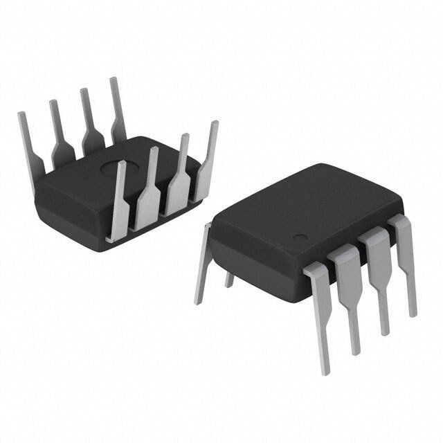
| 产品图片 |
|
| rohs | 符合RoHS无铅 / 符合限制有害物质指令(RoHS)规范要求 |
| 产品系列 | 放大器 IC,运算放大器 - 运放,Texas Instruments TLC2202IPLinCMOS™ |
| 数据手册 | |
| 产品型号 | TLC2202IP |
| PCN设计/规格 | |
| 产品目录页面 | |
| 产品种类 | 运算放大器 - 运放 |
| 供应商器件封装 | 8-PDIP |
| 共模抑制比—最小值 | 75 dB |
| 关闭 | No Shutdown |
| 其它名称 | 296-7073-5 |
| 包装 | 管件 |
| 单位重量 | 440.400 mg |
| 压摆率 | 2.7 V/µs |
| 双重电源电压 | +/- 3 V, +/- 5 V |
| 商标 | Texas Instruments |
| 增益带宽生成 | 1.9 MHz |
| 增益带宽积 | 1.9MHz |
| 安装类型 | 通孔 |
| 安装风格 | Through Hole |
| 封装 | Tube |
| 封装/外壳 | 8-DIP(0.300",7.62mm) |
| 封装/箱体 | PDIP-8 |
| 工作温度 | -40°C ~ 85°C |
| 工作电源电压 | 4.6 V to 16 V, +/- 2.3 V to +/- 8 V |
| 工厂包装数量 | 50 |
| 技术 | LinCMOS |
| 放大器类型 | 通用 |
| 最大双重电源电压 | +/- 8 V |
| 最大工作温度 | + 85 C |
| 最小双重电源电压 | +/- 2.3 V |
| 最小工作温度 | - 40 C |
| 标准包装 | 50 |
| 电压-电源,单/双 (±) | 4.6 V ~ 16 V, ±2.3 V ~ 8 V |
| 电压-输入失调 | 100µV |
| 电流-电源 | 1.8mA |
| 电流-输入偏置 | 1pA |
| 电流-输出/通道 | 50mA |
| 电源电流 | 2.7 mA |
| 电路数 | 2 |
| 系列 | TLC2202 |
| 转换速度 | 2.7 V/us |
| 输入偏压电流—最大 | 100 pA |
| 输入参考电压噪声 | 18 nV |
| 输入补偿电压 | 1 mV |
| 输出电流 | 50 mA |
| 输出类型 | 满摆幅 |
| 通道数量 | 2 Channel |


PDF Datasheet 数据手册内容提取
(cid:1)(cid:2)(cid:3)(cid:4)(cid:4)(cid:5)(cid:6)(cid:7) (cid:1)(cid:2)(cid:3)(cid:4)(cid:4)(cid:5)(cid:6)(cid:8)(cid:7) (cid:1)(cid:2)(cid:3)(cid:4)(cid:4)(cid:5)(cid:6)(cid:9)(cid:7) (cid:1)(cid:2)(cid:3)(cid:4)(cid:4)(cid:5)(cid:6)(cid:10) (cid:8)(cid:11)(cid:12)(cid:13)(cid:14)(cid:15)(cid:16)(cid:11) (cid:2)(cid:17)(cid:14)(cid:3)(cid:18)(cid:19)(cid:20) (cid:2)(cid:19)(cid:21)(cid:22)(cid:23)(cid:19)(cid:24)(cid:20)(cid:25) (cid:26)(cid:27)(cid:25)(cid:3)(cid:24)(cid:20)(cid:24)(cid:19)(cid:23) (cid:19)(cid:26)(cid:25)(cid:27)(cid:8)(cid:1)(cid:24)(cid:19)(cid:23)(cid:8)(cid:2) (cid:8)(cid:18)(cid:26)(cid:2)(cid:24)(cid:28)(cid:24)(cid:25)(cid:27)(cid:20) SLOS175B − FEBRUARY 1997 − REVISED JANUARY 2008 (cid:1) (cid:1) B Grade Is 100% Tested for Noise Low Input Bias Current 30 nV/√Hz Max at f = 10 Hz 1 pA Typ at T = 25°C A 12 nV/√Hz Max at f = 1 kHz (cid:1) Common-Mode Input Voltage Range (cid:1) Low Input Offset Voltage...500 µV Max Includes the Negative Rail (cid:1) (cid:1) Excellent Offset Voltage Stability Fully Specified For Both Single-Supply and With Temperature...0.5 µV/°C Typ Split-Supply Operation (cid:1) Rail-to-Rail Output Swing TYPICAL EQUIVALENT description INPUT NOISE VOLTAGE vs The TLC220x, TLC220xA, TLC220xB, and FREQUENCY TLC220xY are precision, low-noise operational 60 amplifiers using Texas Instruments Advanced Hzz VDD = 5 V LnionisCeM OpeSrfo rpmroacnecses . oTfh ethsee dleovwiceesst- ncoomiseb inJeF tEhTe nV/ H 50 TRAS == 2250° CΩ − amplifiers with the dc precision available e g previously only in bipolar amplifiers. The a Advanced LinCMOS process uses silicon-gate Volt 40 e technology to obtain input offset voltage stability s oi with temperature and time that far exceeds that N 30 obtainable using metal-gate technology. In ut p n addition, this technology makes possible input nt I 20 impedance levels that meet or exceed levels e al offered by top-gate JFET and expensive v ui dielectric-isolated devices. Eq 10 − The combination of excellent DC and noise n n VV performance with a common-mode input voltage 0 range that includes the negative rail makes these 1 10 100 1 k 10 k devices an ideal choice for high-impedance, f − Frequency − Hz low-level signal-conditioning applications in either single-supply or split-supply configurations. The device inputs and outputs are designed to withstand −100-mA surge currents without sustaining latch-up. In addition, internal ESD-protection circuits prevent functional failures at voltages up to 2000 V as tested under MIL-PRF-38535, Method 3015.2; however, care should be exercised in handling these devices as exposure to ESD may result in degradation of the parametric performance. The C-suffix devices are characterized for operation from 0°C to 70°C. The I-suffix devices are characterized for operation from −40°C to 85°C. The M-suffix devices are characterized for operation over the full military temperature range of −55°C to 125°C. Please be aware that an important notice concerning availability, standard warranty, and use in critical applications of TexasInstruments semiconductor products and disclaimers thereto appears at the end of this data sheet. Advanced LinCMOS is a trademark of Texas Instruments Incorporated. All other trademarks are the property of their respective owners. (cid:26)(cid:27)(cid:19)/0(cid:3)(cid:1)(cid:24)(cid:19)(cid:23) /(cid:8)(cid:1)(cid:8) (cid:17)(cid:14).(cid:31)(cid:30)$(cid:13)"(cid:17)(cid:31)(cid:14) (cid:17)# (cid:15)!(cid:30)(cid:30)(cid:16)(cid:14)" (cid:13)# (cid:31). (cid:29)!1%(cid:17)(cid:15)(cid:13)"(cid:17)(cid:31)(cid:14) (cid:11)(cid:13)"(cid:16)+ Copyright 1997−2008, Texas Instruments Incorporated (cid:26)(cid:30)(cid:31)(cid:11)!(cid:15)"# (cid:15)(cid:31)(cid:14).(cid:31)(cid:30)$ "(cid:31) #(cid:29)(cid:16)(cid:15)(cid:17).(cid:17)(cid:15)(cid:13)"(cid:17)(cid:31)(cid:14)# (cid:29)(cid:16)(cid:30) ")(cid:16) "(cid:16)(cid:30)$# (cid:31). (cid:1)(cid:16)(cid:6)(cid:13)# (cid:24)(cid:14)#"(cid:30)!$(cid:16)(cid:14)"# #"(cid:13)(cid:14)(cid:11)(cid:13)(cid:30)(cid:11) *(cid:13)(cid:30)(cid:30)(cid:13)(cid:14)"-+ (cid:26)(cid:30)(cid:31)(cid:11)!(cid:15)"(cid:17)(cid:31)(cid:14) (cid:29)(cid:30)(cid:31)(cid:15)(cid:16)##(cid:17)(cid:14), (cid:11)(cid:31)(cid:16)# (cid:14)(cid:31)" (cid:14)(cid:16)(cid:15)(cid:16)##(cid:13)(cid:30)(cid:17)%- (cid:17)(cid:14)(cid:15)%!(cid:11)(cid:16) (cid:19)(cid:14) (cid:29)(cid:30)(cid:31)(cid:11)!(cid:15)"# (cid:15)(cid:31)$(cid:29)%(cid:17)(cid:13)(cid:14)" "(cid:31) (cid:18)(cid:24)(cid:2)(cid:22)(cid:26)(cid:27)(cid:28)(cid:22)&’(&((cid:7) (cid:13)%% (cid:29)(cid:13)(cid:30)(cid:13)$(cid:16)"(cid:16)(cid:30)# (cid:13)(cid:30)(cid:16) "(cid:16)#"(cid:16)(cid:11) "(cid:16)#"(cid:17)(cid:14), (cid:31). (cid:13)%% (cid:29)(cid:13)(cid:30)(cid:13)$(cid:16)"(cid:16)(cid:30)#+ !(cid:14)%(cid:16)## (cid:31)")(cid:16)(cid:30)*(cid:17)#(cid:16) (cid:14)(cid:31)"(cid:16)(cid:11)+ (cid:19)(cid:14) (cid:13)%% (cid:31)")(cid:16)(cid:30) (cid:29)(cid:30)(cid:31)(cid:11)!(cid:15)"#(cid:7) (cid:29)(cid:30)(cid:31)(cid:11)!(cid:15)"(cid:17)(cid:31)(cid:14) (cid:29)(cid:30)(cid:31)(cid:15)(cid:16)##(cid:17)(cid:14), (cid:11)(cid:31)(cid:16)# (cid:14)(cid:31)" (cid:14)(cid:16)(cid:15)(cid:16)##(cid:13)(cid:30)(cid:17)%- (cid:17)(cid:14)(cid:15)%!(cid:11)(cid:16) "(cid:16)#"(cid:17)(cid:14), (cid:31). (cid:13)%% (cid:29)(cid:13)(cid:30)(cid:13)$(cid:16)"(cid:16)(cid:30)#+ POST OFFICE BOX 655303 • DALLAS, TEXAS 75265 1
(cid:1)(cid:2)(cid:3)(cid:4)(cid:4)(cid:5)(cid:6)(cid:7) (cid:1)(cid:2)(cid:3)(cid:4)(cid:4)(cid:5)(cid:6)(cid:8)(cid:7) (cid:1)(cid:2)(cid:3)(cid:4)(cid:4)(cid:5)(cid:6)(cid:9)(cid:7) (cid:1)(cid:2)(cid:3)(cid:4)(cid:4)(cid:5)(cid:6)(cid:10) (cid:8)(cid:11)(cid:12)(cid:13)(cid:14)(cid:15)(cid:16)(cid:11) (cid:2)(cid:17)(cid:14)(cid:3)(cid:18)(cid:19)(cid:20) (cid:2)(cid:19)(cid:21)(cid:22)(cid:23)(cid:19)(cid:24)(cid:20)(cid:25) (cid:26)(cid:27)(cid:25)(cid:3)(cid:24)(cid:20)(cid:24)(cid:19)(cid:23) (cid:19)(cid:26)(cid:25)(cid:27)(cid:8)(cid:1)(cid:24)(cid:19)(cid:23)(cid:8)(cid:2) (cid:8)(cid:18)(cid:26)(cid:2)(cid:24)(cid:28)(cid:24)(cid:25)(cid:27)(cid:20) SLOS175B − FEBRUARY 1997 − REVISED JANUARY 2008 TLC2201 AVAILABLE OPTIONS PACKAGED DEVICES TA AVTIO 2m5a°Cx fA VV=Tnn 1mm205aa °HxxCz fA VV=Tnn 1mm2 5kaa°HxxCz OSUMTLAILNLE† CACRHRIPIER CERDAIPMIC PLADSIPTIC FCCO(HHRYII)MPP‡ (D) (FK) (JG) (P) 200 µV 35 nV/√Hz 15 nV/√Hz TLC2201ACD TLC2201ACP 00°CC ttoo 7700°CC 200 µV 30 nV/√Hz 12 nV/√Hz TLC2201BCD —— —— TLC2201BCP TTLLCC22220011YY 500 µV — — TLC2201CD TLC2201CP 200 µV 35 nV/√Hz 15 nV/√Hz TLC2201AID TLC2201AIP −−4400°CC ttoo 8855°CC 200 µV 30 nV/√Hz 12 nV/√Hz TLC2201BID —— —— TLC2201BIP —— 500 µV — — TLC2201ID TLC2201IP 200 µV 35 nV/√Hz 15 nV/√Hz TLC2201AMD TLC2201AMFK TLC2201AMJG TLC2201AMP −−5555°CC ttoo 112255°CC 200 µV 30 nV/√Hz 12 nV/√Hz TLC2201BMD TLC2201BMFK TLC2201BMJG TLC2201BMP —— 500 µV — — TLC2201MD TLC2201MFK TLC2201MJG TLC2201MP †The D packages are available taped and reeled. Add R suffix to device type (e.g. TLC220xBCDR). ‡Chip forms are tested at 25°C only. TLC2202 AVAILABLE OPTIONS PACKAGED DEVICES TA AVTIO 2m5a°Cx fA V=Tn 1m205a °HxCz fA V=Tn 1m2 5ka°HxCz OSUMTLAILNLE† OPSLUMATASLLITNLICE CACRHRIPIER CERDAIPMIC PLADSIPTIC FCO(HRYI)MP‡ (D) (FK) (JG) (P) (PS) 500 µV 30 nV/√Hz 12 nV/√Hz TLC2202BCD — — — TLC2202BCP 00°CC ttoo 7700°CC 500 µV 35 nV/√Hz 15 nV/√Hz TLC2202ACD — — — TLC2202ACP TTLLCC22220022YY 1 mV — — TLC2202CD TLC2202CPSR — — TLC2202CP 500 µV 30 nV/√Hz 12 nV/√Hz TLC2202BID — — — TLC2202BIP −−4400°CC ttoo 8855°CC 500 µV 35 nV/√Hz 15 nV/√Hz TLC2202AID — — — TLC2202AIP —— 1 mV — — TLC2202ID — — — TLC2202IP 500 µV 30 nV/√Hz 12 nV/√Hz TLC2202BMD — TLC2202BMFK TLC2202BMJG TLC2202BMP −−5555°CC ttoo 112255°CC 500 µV 35 nV/√Hz 15 nV/√Hz TLC2202AMD — TLC2202AMFK TLC2202AMJG TLC2202AMP —— 1 mV — — TLC2202MD — TLC2202MFK TLC2202MJG TLC2202MP †The D packages are available taped and reeled. Add R suffix to device type (e.g. TLC220xBCDR). ‡Chip forms are tested at 25°C only. 2 POST OFFICE BOX 655303 • DALLAS, TEXAS 75265
(cid:1)(cid:2)(cid:3)(cid:4)(cid:4)(cid:5)(cid:6)(cid:7) (cid:1)(cid:2)(cid:3)(cid:4)(cid:4)(cid:5)(cid:6)(cid:8)(cid:7) (cid:1)(cid:2)(cid:3)(cid:4)(cid:4)(cid:5)(cid:6)(cid:9)(cid:7) (cid:1)(cid:2)(cid:3)(cid:4)(cid:4)(cid:5)(cid:6)(cid:10) (cid:8)(cid:11)(cid:12)(cid:13)(cid:14)(cid:15)(cid:16)(cid:11) (cid:2)(cid:17)(cid:14)(cid:3)(cid:18)(cid:19)(cid:20) (cid:2)(cid:19)(cid:21)(cid:22)(cid:23)(cid:19)(cid:24)(cid:20)(cid:25) (cid:26)(cid:27)(cid:25)(cid:3)(cid:24)(cid:20)(cid:24)(cid:19)(cid:23) (cid:19)(cid:26)(cid:25)(cid:27)(cid:8)(cid:1)(cid:24)(cid:19)(cid:23)(cid:8)(cid:2) (cid:8)(cid:18)(cid:26)(cid:2)(cid:24)(cid:28)(cid:24)(cid:25)(cid:27)(cid:20) SLOS175B − FEBRUARY 1997 − REVISED JANUARY 2008 TLC2201 TLC2202 TLC2202 D, JG, OR P PACKAGE PS, JG, OR P PACKAGE D PACKAGE (TOP VIEW) (TOP VIEW) (TOP VIEW) NC 1 8 NC 1OUT 1 8 VDD+ NC 1 14 NC IN− 2 7 VDD+ 1IN− 2 7 2OUT NC 2 13 NC IN+ 3 6 OUT 1IN+ 3 6 2IN− 1OUT 3 12 VDD+ VDD−/GND 4 5 NC VDD−/GND 4 5 2IN+ 1IN− 4 11 2OUT 1IN+ 5 10 2IN− VDD−/GND 6 9 2IN+ NC 7 8 NC TLC2201 TLC2202 FK PACKAGE FK PACKAGE (TOP VIEW) (TOP VIEW) C C C CC T + N N N NN U D C O C DC N 1 NV N 3 2 1 20 19 NC 4 18 NC 3 2 1 20 19 IN− 5 17 VDD+ NC 4 18 NC NC 6 16 NC 1IN− 5 17 2OUT IN+ 7 15 OUT NC 6 16 NC NC 8 14 NC 1IN+ 7 15 2IN− 9 10 11 12 13 NC 8 14 NC 9 10 11 12 13 C D CC C N GN NN N NC ND NCN+ NC /− G 2I D / − VD D D V NC − No internal connection POST OFFICE BOX 655303 • DALLAS, TEXAS 75265 3
(cid:1)(cid:2)(cid:3)(cid:4)(cid:4)(cid:5)(cid:6)(cid:7) (cid:1)(cid:2)(cid:3)(cid:4)(cid:4)(cid:5)(cid:6)(cid:8)(cid:7) (cid:1)(cid:2)(cid:3)(cid:4)(cid:4)(cid:5)(cid:6)(cid:9)(cid:7) (cid:1)(cid:2)(cid:3)(cid:4)(cid:4)(cid:5)(cid:6)(cid:10) (cid:8)(cid:11)(cid:12)(cid:13)(cid:14)(cid:15)(cid:16)(cid:11) (cid:2)(cid:17)(cid:14)(cid:3)(cid:18)(cid:19)(cid:20) (cid:2)(cid:19)(cid:21)(cid:22)(cid:23)(cid:19)(cid:24)(cid:20)(cid:25) (cid:26)(cid:27)(cid:25)(cid:3)(cid:24)(cid:20)(cid:24)(cid:19)(cid:23) (cid:19)(cid:26)(cid:25)(cid:27)(cid:8)(cid:1)(cid:24)(cid:19)(cid:23)(cid:8)(cid:2) (cid:8)(cid:18)(cid:26)(cid:2)(cid:24)(cid:28)(cid:24)(cid:25)(cid:27)(cid:20) SLOS175B − FEBRUARY 1997 − REVISED JANUARY 2008 equivalent schematic (each amplifier) VDD+ Q3 Q6 Q9 Q12 Q14 Q16 IN + OUT C1 IN − Q1 Q4 Q13 Q15 Q17 D1 Q7 Q8 Q10 Q11 R1 R2 Q2 Q5 VDD−/GND ACTUAL DEVICE COMPONENT COUNT COMPONENT TLC2201 TLC2202 Transistors 17 34 Resistors 2 2 Diodes 1 4 Capacitors 1 2 4 POST OFFICE BOX 655303 • DALLAS, TEXAS 75265
(cid:1)(cid:2)(cid:3)(cid:4)(cid:4)(cid:5)(cid:6)(cid:7) (cid:1)(cid:2)(cid:3)(cid:4)(cid:4)(cid:5)(cid:6)(cid:8)(cid:7) (cid:1)(cid:2)(cid:3)(cid:4)(cid:4)(cid:5)(cid:6)(cid:9)(cid:7) (cid:1)(cid:2)(cid:3)(cid:4)(cid:4)(cid:5)(cid:6)(cid:10) (cid:8)(cid:11)(cid:12)(cid:13)(cid:14)(cid:15)(cid:16)(cid:11) (cid:2)(cid:17)(cid:14)(cid:3)(cid:18)(cid:19)(cid:20) (cid:2)(cid:19)(cid:21)(cid:22)(cid:23)(cid:19)(cid:24)(cid:20)(cid:25) (cid:26)(cid:27)(cid:25)(cid:3)(cid:24)(cid:20)(cid:24)(cid:19)(cid:23) (cid:19)(cid:26)(cid:25)(cid:27)(cid:8)(cid:1)(cid:24)(cid:19)(cid:23)(cid:8)(cid:2) (cid:8)(cid:18)(cid:26)(cid:2)(cid:24)(cid:28)(cid:24)(cid:25)(cid:27)(cid:20) SLOS175B − FEBRUARY 1997 − REVISED JANUARY 2008 TLC2201Y chip information This chip, when properly assembled, displays characteristics similar to the TLC2201C. Thermal compression or ultrasonic bonding may be used on the doped-aluminum bonding path. Chips may be mounted with conductive epoxy or a gold-silicon preform. BONDING PAD ASSIGNMENTS VDD+ (7) (2) (8) (7) (6) IN− + (6) (3) OUT IN+ − (4) VDD− 77 CHIP THICKNESS: 15 MILS TYPICAL BONDING PADS: 4 × 4 MILS MINIMUM TJmax = 150°C TOLERANCES ARE ±10%. ALL DIMENSIONS ARE IN MILS. (1) (2) (3) (4) PIN (4) IS INTERNALLY CONNECTED TO BACK SIDE OF CHIP. TERMINAL NUMBERS ARE FOR THE 65 D, JG, AND P PACKAGES. POST OFFICE BOX 655303 • DALLAS, TEXAS 75265 5
(cid:1)(cid:2)(cid:3)(cid:4)(cid:4)(cid:5)(cid:6)(cid:7) (cid:1)(cid:2)(cid:3)(cid:4)(cid:4)(cid:5)(cid:6)(cid:8)(cid:7) (cid:1)(cid:2)(cid:3)(cid:4)(cid:4)(cid:5)(cid:6)(cid:9)(cid:7) (cid:1)(cid:2)(cid:3)(cid:4)(cid:4)(cid:5)(cid:6)(cid:10) (cid:8)(cid:11)(cid:12)(cid:13)(cid:14)(cid:15)(cid:16)(cid:11) (cid:2)(cid:17)(cid:14)(cid:3)(cid:18)(cid:19)(cid:20) (cid:2)(cid:19)(cid:21)(cid:22)(cid:23)(cid:19)(cid:24)(cid:20)(cid:25) (cid:26)(cid:27)(cid:25)(cid:3)(cid:24)(cid:20)(cid:24)(cid:19)(cid:23) (cid:19)(cid:26)(cid:25)(cid:27)(cid:8)(cid:1)(cid:24)(cid:19)(cid:23)(cid:8)(cid:2) (cid:8)(cid:18)(cid:26)(cid:2)(cid:24)(cid:28)(cid:24)(cid:25)(cid:27)(cid:20) SLOS175B − FEBRUARY 1997 − REVISED JANUARY 2008 TLC2202Y chip formation This chip, when properly assembled, displays characteristics similar to the TLC2202C. Thermal compression or ultrasonic bonding may be used on the doped-aluminum bonding pads. Chips may be mounted with conductive epoxy or a gold-silicon preform. BONDING PAD ASSIGNMENTS VDD+ (8) (7) (6) (8) (3) 1IN+ + (1) 1OUT (2) 1IN− − (5) + 2IN+ (7) (5) 2OUT (6) − 2IN− (4) 80 VDD− CHIP THICKNESS: 15 MILS TYPICAL BONDING PADS: 4 × 4 MILS MINIMUM TJmax = 150°C (4) TOLERANCES ARE ±10%. ALL DIMENSIONS ARE IN MILS. (1) (2) (3) PIN (4) IS INTERNALLY CONNECTED TO BACKSIDE OF CHIP. 100 6 POST OFFICE BOX 655303 • DALLAS, TEXAS 75265
(cid:1)(cid:2)(cid:3)(cid:4)(cid:4)(cid:5)(cid:6)(cid:7) (cid:1)(cid:2)(cid:3)(cid:4)(cid:4)(cid:5)(cid:6)(cid:8)(cid:7) (cid:1)(cid:2)(cid:3)(cid:4)(cid:4)(cid:5)(cid:6)(cid:9)(cid:7) (cid:1)(cid:2)(cid:3)(cid:4)(cid:4)(cid:5)(cid:6)(cid:10) (cid:8)(cid:11)(cid:12)(cid:13)(cid:14)(cid:15)(cid:16)(cid:11) (cid:2)(cid:17)(cid:14)(cid:3)(cid:18)(cid:19)(cid:20) (cid:2)(cid:19)(cid:21)(cid:22)(cid:23)(cid:19)(cid:24)(cid:20)(cid:25) (cid:26)(cid:27)(cid:25)(cid:3)(cid:24)(cid:20)(cid:24)(cid:19)(cid:23) (cid:19)(cid:26)(cid:25)(cid:27)(cid:8)(cid:1)(cid:24)(cid:19)(cid:23)(cid:8)(cid:2) (cid:8)(cid:18)(cid:26)(cid:2)(cid:24)(cid:28)(cid:24)(cid:25)(cid:27)(cid:20) SLOS175B − FEBRUARY 1997 − REVISED JANUARY 2008 absolute maximum ratings over operating free-air temperature range (unless otherwise noted)† Supply voltage, V (see Note 1) . . . . . . . . . . . . . . . . . . . . . . . . . . . . . . . . . . . . . . . . . . . . . . . . . . . . . . . . . . . . 8 V DD+ Supply voltage, V . . . . . . . . . . . . . . . . . . . . . . . . . . . . . . . . . . . . . . . . . . . . . . . . . . . . . . . . . . . . . . . . . . . . . . −8 V DD− Differential input voltage, V (see Note 2) . . . . . . . . . . . . . . . . . . . . . . . . . . . . . . . . . . . . . . . . . . . . . . . . . . . ±16 V ID Input voltage, V (any input) . . . . . . . . . . . . . . . . . . . . . . . . . . . . . . . . . . . . . . . . . . . . . . . . . . . . . . . . . . . . . . . . . ±8 V I Input current, I (each input) . . . . . . . . . . . . . . . . . . . . . . . . . . . . . . . . . . . . . . . . . . . . . . . . . . . . . . . . . . . . . . . ±5 mA I Output current, I (each output) . . . . . . . . . . . . . . . . . . . . . . . . . . . . . . . . . . . . . . . . . . . . . . . . . . . . . . . . . . ±50 mA O Duration of short-circuit current at (or below) 25°C (see Note 3) . . . . . . . . . . . . . . . . . . . . . . . . . . . . . . unlimited Continuous total dissipation . . . . . . . . . . . . . . . . . . . . . . . . . . . . . . . . . . . . . . . . . . . See Dissipation Rating Table Operating free-air temperature range, T : C suffix . . . . . . . . . . . . . . . . . . . . . . . . . . . . . . . . . . . . . . . 0°C to 70°C A I suffix . . . . . . . . . . . . . . . . . . . . . . . . . . . . . . . . . . . . . . −40°C to 85°C M suffix . . . . . . . . . . . . . . . . . . . . . . . . . . . . . . . . . . . . −55°C to 125°C Storage temperature range . . . . . . . . . . . . . . . . . . . . . . . . . . . . . . . . . . . . . . . . . . . . . . . . . . . . . . . . −65°C to 150°C Case temperature for 60 seconds: FK package . . . . . . . . . . . . . . . . . . . . . . . . . . . . . . . . . . . . . . . . . . . . . . 260°C Lead temperature 1,6 mm (1/16 inch) from case for 10 seconds: D, PS, or P package . . . . . . . . . . . . 260°C Lead temperature 1,6 mm (1/16 inch) from case for 60 seconds: JG package . . . . . . . . . . . . . . . . . . . . 300°C †Stresses beyond those listed under “absolute maximum ratings” may cause permanent damage to the device. These are stress ratings only, and functional operation of the device at these or any other conditions beyond those indicated under “recommended operating conditions” is not implied. Exposure to absolute-maximum-rated conditions for extended periods may affect device reliability. NOTES: 1. All voltage values except differential voltages are with respect to the midpoint between VDD+ and VDD− . 2. Differential voltages are at IN+ with respect to IN−. 3. The output may be shorted to either supply. Temperature and/or supply voltages must be limited to ensure that the maximum dissipation rating in not exceeded. DISSIPATION RATING TABLE TTAA ≤≤ 2255°CC DDEERRAATTIINNGG FFAACCTTOORR TTAA == 7700°CC TTAA == 8855°CC TTAA == 112255°CC PPAACCKKAAGGEE POWER RATING ABOVE TA = 25°C POWER RATING POWER RATING POWER RATING D−8 725 mW 5.8 mW/°C 464 mW 377 mW 145 mW D−14 950 mW 7.6 mW/°C 608 mW 494 mW 190 mW PS 770 mW 6.2 mW/°C 496 mW 403 mW 155 mW FK 1375 mW 11.0 mW/°C 880 mW 715 mW 275 mW JG 1050 mW 8.4 mW/°C 672 mW 546 mW 210 mW P 1000 mW 8.0 mW/°C 640 mW 520 mW 200 mW recommended operating conditions C SUFFIX I SUFFIX M SUFFIX UUNNIITT MIN MAX MIN MAX MIN MAX Supply voltage, VDD± ±2.3 ±8 ±2.3 ±8 ±2.3 ±8 V Common-mode input voltage, VIC VDD− VDD+ −2.3 VDD− VDD+ −2.3 VDD− VDD+ −2.3 V Operating free-air temperature, TA 0 70 −40 85 −55 125 °C POST OFFICE BOX 655303 • DALLAS, TEXAS 75265 7
(cid:1)(cid:2)(cid:3)(cid:4)(cid:4)(cid:5)(cid:6)(cid:7) (cid:1)(cid:2)(cid:3)(cid:4)(cid:4)(cid:5)(cid:6)(cid:8)(cid:7) (cid:1)(cid:2)(cid:3)(cid:4)(cid:4)(cid:5)(cid:6)(cid:9)(cid:7) (cid:1)(cid:2)(cid:3)(cid:4)(cid:4)(cid:5)(cid:6)(cid:10) (cid:8)(cid:11)(cid:12)(cid:13)(cid:14)(cid:15)(cid:16)(cid:11) (cid:2)(cid:17)(cid:14)(cid:3)(cid:18)(cid:19)(cid:20) (cid:2)(cid:19)(cid:21)(cid:22)(cid:23)(cid:19)(cid:24)(cid:20)(cid:25) (cid:26)(cid:27)(cid:25)(cid:3)(cid:24)(cid:20)(cid:24)(cid:19)(cid:23) (cid:19)(cid:26)(cid:25)(cid:27)(cid:8)(cid:1)(cid:24)(cid:19)(cid:23)(cid:8)(cid:2) (cid:8)(cid:18)(cid:26)(cid:2)(cid:24)(cid:28)(cid:24)(cid:25)(cid:27)(cid:20) SLOS175B − FEBRUARY 1997 − REVISED JANUARY 2008 TLC2201C electrical characteristics at specified free-air temperature, VDD± = ±5 V (unless otherwise noted) TLC2201C PPAARRAAMMEETTEERR TTEESSTT CCOONNDDIITTIIOONNSS TTAA†† UUNNIITT MIN TYP MAX 25°C 100 500 VVIIOO IInnppuutt ooffffsseett vvoollttaaggee µVV Full range 600 αVVIIOO TTeemmppeerraattuurree ccooeeffffiicciieenntt ooff iinnppuutt ooffffsseett vvoollttaaggee FFuullll rraannggee 00..55 µVV//°°CC Input offset voltage long-term drift (see Note 4) 25°C 0.001 0.005 µV/mo VVIICC == 00,, RRSS == 5500 ΩΩ 25°C 0.5 60 IIIIOO IInnppuutt ooffffsseett ccuurrrreenntt ppAA Full range 100 25°C 1 60 IIIIBB IInnppuutt bbiiaass ccuurrrreenntt ppAA Full range 100 −−55 VVIICCRR CCoommmmoonn--mmooddee iinnppuutt vvoollttaaggee rraannggee RRSS == 5500 ΩΩ FFuullll rraannggee ttoo VV 2.7 25°C 4.7 4.8 VVOOMM++ MMaaxxiimmuumm ppoossiittiivvee ppeeaakk oouuttppuutt vvoollttaaggee sswwiinngg VV Full range 4.7 RRLL == 1100 kkΩΩ 25°C −4.7 −4.9 VVOOMM−− MMaaxxiimmuumm nneeggaattiivvee ppeeaakk oouuttppuutt vvoollttaaggee sswwiinngg VV Full range −4.7 25°C 400 560 VVOO == ±±44 VV,, RRLL == 550000 kkΩΩ Full range 300 AAVVDD LLaarrggee--ssiiggnnaall ddiiffffeerreennttiiaall vvoollttaaggee aammpplliiffiiccaattiioonn 25°C 90 100 VV//mmVV VVOO == ±±44 VV,, RRLL == 1100 kkΩΩ Full range 70 VVIICC == VVIICCRRmmiinn,, VVOO == 00,, CCMMRRRR CCoommmmoonn--mmooddee rreejjeeccttiioonn rraattiioo RS = 50 Ω FFuullll rraannggee 8855 ddBB 25°C 90 110 kkSSVVRR SSuuppppllyy vvoollttaaggee rreejjeeccttiioonn rraattiioo ((∆∆VVDDDD± //∆∆VVIIOO)) VVDDDD± == ±±22..33 VV ttoo ±±88 VV ddBB Full range 85 25°C 1.1 1.5 IIDDDD SSuuppppllyy ccuurrrreenntt VVOO == 00,, NNoo llooaadd mmAA Full range 1.5 †Full range is 0°C to +70°C. NOTE 4: Typical values are based on the input offset voltage shift observed through 168 hours of operating life test at TA = 150°C extrapolated to TA = 25°C using the Arrhenius equation and assuming an activation energy of 0.96 eV. TLC2201C operating characteristics at specified free-air temperature, VDD± = ±5 V TLC2201C PPAARRAAMMEETTEERR TTEESSTT CCOONNDDIITTIIOONNSS TTAA†† UUNNIITT MIN TYP MAX VVOO == ±22..33 VV,, RRLL == 1100 kkΩ,, 25°C 2 2.7 SSRR SSlleeww rraattee aatt uunniittyy ggaaiinn CCL == 110000 ppFF Full range 1.5 VV//µss f = 10 Hz 25°C 18 VVnn EEqquuiivvaalleenntt iinnppuutt nnooiissee vvoollttaaggee f = 1 kHz 25°C 8 nnVV//√√HHzz f = 0.1 to 1 Hz 25°C 0.5 VVNN((PPPP)) PPeeaakk--ttoo--ppeeaakk eeqquuiivvaalleenntt iinnppuutt nnooiissee vvoollttaaggee f = 0.1 to 10 Hz 25°C 0.7 µVV In Equivalent input noise current 25°C 0.6 fA/√Hz ff == 1100 kkHHzz,, RRLL == 1100 kkΩΩ,, GGaaiinn--bbaannddwwiiddtthh pprroodduucctt 2255°°CC 11..99 MMHHzz CCL == 110000 ppFF φm Phase margin at unity gain RL = 10 kΩ, CL = 100 pF 25°C 48° †Full range is 0°C to +70°C. 8 POST OFFICE BOX 655303 • DALLAS, TEXAS 75265
(cid:1)(cid:2)(cid:3)(cid:4)(cid:4)(cid:5)(cid:6)(cid:7) (cid:1)(cid:2)(cid:3)(cid:4)(cid:4)(cid:5)(cid:6)(cid:8)(cid:7) (cid:1)(cid:2)(cid:3)(cid:4)(cid:4)(cid:5)(cid:6)(cid:9)(cid:7) (cid:1)(cid:2)(cid:3)(cid:4)(cid:4)(cid:5)(cid:6)(cid:10) (cid:8)(cid:11)(cid:12)(cid:13)(cid:14)(cid:15)(cid:16)(cid:11) (cid:2)(cid:17)(cid:14)(cid:3)(cid:18)(cid:19)(cid:20) (cid:2)(cid:19)(cid:21)(cid:22)(cid:23)(cid:19)(cid:24)(cid:20)(cid:25) (cid:26)(cid:27)(cid:25)(cid:3)(cid:24)(cid:20)(cid:24)(cid:19)(cid:23) (cid:19)(cid:26)(cid:25)(cid:27)(cid:8)(cid:1)(cid:24)(cid:19)(cid:23)(cid:8)(cid:2) (cid:8)(cid:18)(cid:26)(cid:2)(cid:24)(cid:28)(cid:24)(cid:25)(cid:27)(cid:20) SLOS175B − FEBRUARY 1997 − REVISED JANUARY 2008 TLC2201C electrical characteristics at specified free-air temperature, VDD± = ±5 V (unless otherwise noted) TLC2201AC TLC2201BC PPAARRAAMMEETTEERR TTEESSTT CCOONNDDIITTIIOONNSS TTAA†† UUNNIITT MIN TYP MAX MIN TYP MAX 25°C 80 200 80 200 VVIIOO IInnppuutt ooffffsseett vvoollttaaggee µVV Full range 300 300 Temperature coefficient of input αVIO offset voltage Full range 0.5 0.5 µV/°C Input offset voltage long-term drift (see Note 4) VIICC = 0, RSS = 50 Ω 25°C 0.001 0.005 0.001 0.005 µV/mo 25°C 0.5 60 0.5 60 IIIIOO IInnppuutt ooffffsseett ccuurrrreenntt ppAA Full range 100 100 25°C 1 60 1 60 IIIIBB IInnppuutt bbiiaass ccuurrrreenntt ppAA Full range 100 100 Common-mode input voltage −5 to −5 to VICR range RS = 50 Ω Full range 2.7 2.7 V MMaaxxiimmuumm ppoossiittiivvee ppeeaakk oouuttppuutt 25°C 4.7 4.8 4.7 4.8 VVOOMM++ voltage swing Full range 4.7 4.7 VV MMaaxxiimmuumm nneeggaattiivvee ppeeaakk oouuttppuutt RRLL == 1100 kkΩΩ 25°C −4.7 −4.9 −4.7 −4.9 VVOOMM−− voltage swing Full range −4.7 −4.7 VV 25°C 400 560 400 560 VVOO == ±±44 VV,, RRLL == 550000 kkΩΩ LLaarrggee--ssiiggnnaall ddiiffffeerreennttiiaall vvoollttaaggee Full range 300 300 AAVVDD aammpplliiffiiccaattiioonn 25°C 90 100 90 100 VV//mmVV VVOO == ±±44 VV,, RRLL == 1100 kkΩΩ Full range 70 70 VIC = VICRmin, 25°C 90 115 90 115 CCMMRRRR CCoommmmoonn--mmooddee rreejjeeccttiioonn rraattiioo ddBB VO = 0, RS = 50 Ω Full range 85 85 SSuuppppllyy vvoollttaaggee rreejjeeccttiioonn rraattiioo 25°C 90 110 90 110 kkSSVVRR (∆VDD± /∆VIO) VVDDDD± == ±±22..33 VV ttoo ±±88 VV Full range 85 85 ddBB 25°C 1.1 1.5 1.1 1.5 IIDDDD SSuuppppllyy ccuurrrreenntt VVOO == 00,, NNoo llooaadd mmAA Full range 1.5 1.5 †Full range is 0°C to +70°C. NOTE 4: Typical values are based on the input offset voltage shift observed through 168 hours of operating life test at TA = 150°C extrapolated to TA = 25°C using the Arrhenius equation and assuming an activation energy of 0.96 eV. POST OFFICE BOX 655303 • DALLAS, TEXAS 75265 9
(cid:1)(cid:2)(cid:3)(cid:4)(cid:4)(cid:5)(cid:6)(cid:7) (cid:1)(cid:2)(cid:3)(cid:4)(cid:4)(cid:5)(cid:6)(cid:8)(cid:7) (cid:1)(cid:2)(cid:3)(cid:4)(cid:4)(cid:5)(cid:6)(cid:9)(cid:7) (cid:1)(cid:2)(cid:3)(cid:4)(cid:4)(cid:5)(cid:6)(cid:10) (cid:8)(cid:11)(cid:12)(cid:13)(cid:14)(cid:15)(cid:16)(cid:11) (cid:2)(cid:17)(cid:14)(cid:3)(cid:18)(cid:19)(cid:20) (cid:2)(cid:19)(cid:21)(cid:22)(cid:23)(cid:19)(cid:24)(cid:20)(cid:25) (cid:26)(cid:27)(cid:25)(cid:3)(cid:24)(cid:20)(cid:24)(cid:19)(cid:23) (cid:19)(cid:26)(cid:25)(cid:27)(cid:8)(cid:1)(cid:24)(cid:19)(cid:23)(cid:8)(cid:2) (cid:8)(cid:18)(cid:26)(cid:2)(cid:24)(cid:28)(cid:24)(cid:25)(cid:27)(cid:20) SLOS175B − FEBRUARY 1997 − REVISED JANUARY 2008 TLC2201C operating characteristics at specified free-air temperature, VDD± = ±5 V TLC2201AC TLC2201BC PPAARRAAMMEETTEERR TTEESSTT CCOONNDDIITTIIOONNSS TTAA†† UUNNIITT MIN TYP MAX MIN TYP MAX SSRR SSlleeww rraattee aatt uunniittyy ggaaiinn VVOO == ±±22..33 VV,, RRLL == 1100 kkΩ,, 25°C 2 2.7 2 2.7 VV//µss CL = 100 pF Full range 1.5 1.5 EEqquuiivvaalleenntt iinnppuutt nnooiissee vvoolltt-- f = 10 Hz 25°C 18 35 18 30 VVnn age (see Note 5) f = 1 kHz 25°C 8 15 8 12 nnVV//√√HHzz PPeeaakk--ttoo--ppeeaakk eeqquuiivvaalleenntt iinnppuutt f = 0.1 to 1 Hz 25°C 0.5 0.5 VVNN((PPPP)) noise voltage f = 0.1 to 10 Hz 25°C 0.7 0.7 µVV In Equivalent input noise current 25°C 0.6 0.6 fA/√Hz ff == 1100 kkHHzz,, RRLL == 1100 kkΩΩ,, GGaaiinn--bbaannddwwiiddtthh pprroodduucctt 2255°°CC 11..99 11..99 MMHHzz CL = 100 pF φm Phase margin at unity gain RL = 10 kΩ, CL = 100 pF 25°C 48° 48° †Full range is 0°C to +70°C. NOTE 5: This parameter is tested on a sample basis for the TLC2201A and on all devices for the TLC2201B. For other test requirements, please contact the factory. This statement has no bearing on testing or nontesting of other parameters. 10 POST OFFICE BOX 655303 • DALLAS, TEXAS 75265
(cid:1)(cid:2)(cid:3)(cid:4)(cid:4)(cid:5)(cid:6)(cid:7) (cid:1)(cid:2)(cid:3)(cid:4)(cid:4)(cid:5)(cid:6)(cid:8)(cid:7) (cid:1)(cid:2)(cid:3)(cid:4)(cid:4)(cid:5)(cid:6)(cid:9)(cid:7) (cid:1)(cid:2)(cid:3)(cid:4)(cid:4)(cid:5)(cid:6)(cid:10) (cid:8)(cid:11)(cid:12)(cid:13)(cid:14)(cid:15)(cid:16)(cid:11) (cid:2)(cid:17)(cid:14)(cid:3)(cid:18)(cid:19)(cid:20) (cid:2)(cid:19)(cid:21)(cid:22)(cid:23)(cid:19)(cid:24)(cid:20)(cid:25) (cid:26)(cid:27)(cid:25)(cid:3)(cid:24)(cid:20)(cid:24)(cid:19)(cid:23) (cid:19)(cid:26)(cid:25)(cid:27)(cid:8)(cid:1)(cid:24)(cid:19)(cid:23)(cid:8)(cid:2) (cid:8)(cid:18)(cid:26)(cid:2)(cid:24)(cid:28)(cid:24)(cid:25)(cid:27)(cid:20) SLOS175B − FEBRUARY 1997 − REVISED JANUARY 2008 TLC2201C electrical characteristics at specified free-air temperature, V = 5 V (unless otherwise DD noted) TLC2201C PPAARRAAMMEETTEERR TTEESSTT CCOONNDDIITTIIOONNSS TTAA†† UUNNIITT MIN TYP MAX 25°C 100 500 VVIIOO IInnppuutt ooffffsseett vvoollttaaggee µVV Full range 600 αVIO Temperature coefficient of input offset voltage Full range 0.5 µV/°C Input offset voltage long-term drift (see Note 4) 25°C 0.001 0.005 µV/mo VVIICC == 00,, RRSS == 5500 ΩΩ 25°C 0.5 60 IIIIOO IInnppuutt ooffffsseett ccuurrrreenntt ppAA Full range 100 25°C 1 60 IIIIBB IInnppuutt bbiiaass ccuurrrreenntt ppAA Full range 100 00 VVIICCRR CCoommmmoonn--mmooddee iinnppuutt vvoollttaaggee rraannggee RRSS == 5500 ΩΩ FFuullll rraannggee ttoo VV 2.7 25°C 4.7 4.8 VVOOHH MMaaxxiimmuumm hhiigghh--lleevveell oouuttppuutt vvoollttaaggee RRLL == 1100 kkΩΩ VV Full range 4.7 25°C 0 50 VVOOLL MMaaxxiimmuumm llooww--lleevveell oouuttppuutt vvoollttaaggee IIOO == 00 mmVV Full range 50 VVOO == 11 VV ttoo 44 VV,, 25°C 150 315 RL = 500 kΩ Full range 100 AAVVDD LLaarrggee--ssiiggnnaall ddiiffffeerreennttiiaall vvoollttaaggee aammpplliiffiiccaattiioonn VVOO == 11 VV ttoo 44 VV,, 25°C 25 55 VV//mmVV RL = 10 kΩ Full range 15 VVIICC == VVIICCRRmmiinn,, VVOO == 00,, 25°C 90 110 CCMMRRRR CCoommmmoonn--mmooddee rreejjeeccttiioonn rraattiioo RS = 50 Ω Full range 85 ddBB 25°C 90 110 kkSSVVRR SSuuppppllyy vvoollttaaggee rreejjeeccttiioonn rraattiioo ((∆∆VVDDDD±//∆∆VVIIOO)) VVDDDD== 44..66 VV ttoo 1166 VV ddBB Full range 85 25°C 1 1.5 IIDDDD SSuuppppllyy ccuurrrreenntt VVOO == 22..55 VV,, NNoo llooaadd mmAA Full range 1.5 †Full range is 0°C to +70°C. NOTE 4: Typical values are based on the input offset voltage shift observed through 168 hours of operating life test at TA = 150°C extrapolated to TA = 25°C using the Arrhenius equation and assuming an activation energy of 0.96 eV. TLC2201C operating characteristics at specified free-air temperature, V = 5 V DD TLC2201C PPAARRAAMMEETTEERR TTEESSTT CCOONNDDIITTIIOONNSS TTAA†† UUNNIITT MIN TYP MAX VO = 0.5 V to 2.5 V, 25°C 1.8 2.5 SSRR SSlleeww rraattee aatt uunniittyy ggaaiinn VV//µss RL = 10 kΩ, CL = 100 pF Full range 1.3 f = 10 Hz 25°C 18 VVnn EEqquuiivvaalleenntt iinnppuutt nnooiissee vvoollttaaggee f = 1 kHz 25°C 8 nnVV//√√HHzz f = 0.1 to 1 Hz 25°C 0.5 VVNN((PPPP)) PPeeaakk--ttoo--ppeeaakk eeqquuiivvaalleenntt iinnppuutt nnooiissee vvoollttaaggee f = 0.1 to 10 Hz 25°C 0.7 µVV In Equivalent input noise current 25°C 0.6 fA/√Hz ff == 1100 kkHHzz,, RRLL == 1100 kkΩΩ,, GGaaiinn--bbaannddwwiiddtthh pprroodduucctt 2255°°CC 11..88 MMHHzz CCL == 110000 ppFF φm Phase margin at unity gain RL = 10 kΩ, CL = 100 pF 25°C 45° †Full range is 0°C to +70°C. POST OFFICE BOX 655303 • DALLAS, TEXAS 75265 11
(cid:1)(cid:2)(cid:3)(cid:4)(cid:4)(cid:5)(cid:6)(cid:7) (cid:1)(cid:2)(cid:3)(cid:4)(cid:4)(cid:5)(cid:6)(cid:8)(cid:7) (cid:1)(cid:2)(cid:3)(cid:4)(cid:4)(cid:5)(cid:6)(cid:9)(cid:7) (cid:1)(cid:2)(cid:3)(cid:4)(cid:4)(cid:5)(cid:6)(cid:10) (cid:8)(cid:11)(cid:12)(cid:13)(cid:14)(cid:15)(cid:16)(cid:11) (cid:2)(cid:17)(cid:14)(cid:3)(cid:18)(cid:19)(cid:20) (cid:2)(cid:19)(cid:21)(cid:22)(cid:23)(cid:19)(cid:24)(cid:20)(cid:25) (cid:26)(cid:27)(cid:25)(cid:3)(cid:24)(cid:20)(cid:24)(cid:19)(cid:23) (cid:19)(cid:26)(cid:25)(cid:27)(cid:8)(cid:1)(cid:24)(cid:19)(cid:23)(cid:8)(cid:2) (cid:8)(cid:18)(cid:26)(cid:2)(cid:24)(cid:28)(cid:24)(cid:25)(cid:27)(cid:20) SLOS175B − FEBRUARY 1997 − REVISED JANUARY 2008 TLC2201C electrical characteristics at specified free-air temperature, V = 5 V (unless otherwise DD noted) TLC2201AC TLC2201BC PPAARRAAMMEETTEERR TTEESSTT CCOONNDDIITTIIOONNSS TTAA†† UUNNIITT MIN TYP MAX MIN TYP MAX 25°C 80 200 80 200 VVIIOO IInnppuutt ooffffsseett vvoollttaaggee µVV Full range 300 300 TTeemmppeerraattuurree ccooeeffffiicciieenntt ooff αVVIIOO input offset voltage FFuullll rraannggee 00..55 00..55 µVV//°°CC Input offset voltage long-term drift (see Note 4) VIC = 0, RS = 50 Ω 25°C 0.001 0.005 0.001 0.005 µV/mo 25°C 0.5 60 0.5 60 IIIIOO IInnppuutt ooffffsseett ccuurrrreenntt ppAA Full range 100 100 25°C 1 60 1 60 IIIIBB IInnppuutt bbiiaass ccuurrrreenntt ppAA Full range 100 100 CCoommmmoonn--mmooddee iinnppuutt vvoollttaaggee 00 ttoo 00 ttoo VVIICCRR range RRSS == 5500 ΩΩ FFuullll rraannggee 2.7 2.7 VV MMaaxxiimmuumm hhiigghh--lleevveell oouuttppuutt 25°C 4.7 4.8 4.7 4.8 VVOOHH voltage RRLL == 1100 kkΩΩ Full range 4.7 4.7 VV MMaaxxiimmuumm llooww--lleevveell oouuttppuutt 25°C 0 50 0 50 VVOOLL voltage IIOO == 00 Full range 50 50 mmVV VVOO == 11 VV ttoo 44 VV,, 25°C 150 315 150 315 LLaarrggee--ssiiggnnaall ddiiffffeerreennttiiaall RL = 500 kΩ Full range 100 100 AAVVDD vvoollttaaggee aammpplliiffiiccaattiioonn VVOO == 11 VV ttoo 44 VV,, 25°C 25 55 25 55 VV//mmVV RL = 10 kΩ Full range 15 15 VIC = VICRmin, 25°C 90 110 90 110 CCMMRRRR CCoommmmoonn--mmooddee rreejjeeccttiioonn rraattiioo ddBB VO = 0, RS = 50 Ω Full range 85 85 SSuuppppllyy vvoollttaaggee rreejjeeccttiioonn rraattiioo 25°C 90 110 90 110 kkSSVVRR (∆VDD±/∆VIO) VVDDDD == 44..66 VV ttoo 1166 VV Full range 85 85 ddBB 25°C 1 1.5 1 1.5 IIDDDD SSuuppppllyy ccuurrrreenntt VVOO == 22..55 VV,, NNoo llooaadd mmAA Full range 1.5 1.5 †Full range is 0°C to +70°C. NOTE 4: Typical values are based on the input offset voltage shift observed through 168 hours of operating life test at TA = 150°C extrapolated to TA = 25°C using the Arrhenius equation and assuming an activation energy of 0.96 eV. 12 POST OFFICE BOX 655303 • DALLAS, TEXAS 75265
(cid:1)(cid:2)(cid:3)(cid:4)(cid:4)(cid:5)(cid:6)(cid:7) (cid:1)(cid:2)(cid:3)(cid:4)(cid:4)(cid:5)(cid:6)(cid:8)(cid:7) (cid:1)(cid:2)(cid:3)(cid:4)(cid:4)(cid:5)(cid:6)(cid:9)(cid:7) (cid:1)(cid:2)(cid:3)(cid:4)(cid:4)(cid:5)(cid:6)(cid:10) (cid:8)(cid:11)(cid:12)(cid:13)(cid:14)(cid:15)(cid:16)(cid:11) (cid:2)(cid:17)(cid:14)(cid:3)(cid:18)(cid:19)(cid:20) (cid:2)(cid:19)(cid:21)(cid:22)(cid:23)(cid:19)(cid:24)(cid:20)(cid:25) (cid:26)(cid:27)(cid:25)(cid:3)(cid:24)(cid:20)(cid:24)(cid:19)(cid:23) (cid:19)(cid:26)(cid:25)(cid:27)(cid:8)(cid:1)(cid:24)(cid:19)(cid:23)(cid:8)(cid:2) (cid:8)(cid:18)(cid:26)(cid:2)(cid:24)(cid:28)(cid:24)(cid:25)(cid:27)(cid:20) SLOS175B − FEBRUARY 1997 − REVISED JANUARY 2008 TLC2201C operating characteristics at specified free-air temperature, V = 5 V DD TLC2201AC TLC2201BC PPAARRAAMMEETTEERR TTEESSTT CCOONNDDIITTIIOONNSS TTAA†† UUNNIITT MIN TYP MAX MIN TYP MAX VO = 0.5 V to 2.5 V, 25°C 1.8 2.5 1.8 2.5 SSRR SSlleeww rraattee aatt uunniittyy ggaaiinn VV//µss RL = 10 kΩ, CL = 100 pF Full range 1.3 1.3 EEqquuiivvaalleenntt iinnppuutt nnooiissee vvoollttaaggee f = 10 Hz 25°C 18 35 18 30 VVnn (see Note 5) f = 1 kHz 25°C 8 15 8 12 nnVV//√√HHzz PPeeaakk--ttoo--ppeeaakk eeqquuiivvaalleenntt iinnppuutt f = 0.1 to 1 Hz 25°C 0.5 0.5 VVNN((PPPP)) noise voltage f = 0.1 to 10 Hz 25°C 0.7 0.7 µVV In Equivalent input noise current 25°C 0.6 0.6 fA/√Hz Gain-bandwidth product f = 10 kHz, RL = 10 kΩ, 25°C 1.8 1.8 MHz CL = 100 pF φm Phase margin at unity gain RL = 10 kΩ, CL = 100 pF 25°C 45° 45° †Full range is 0°C to +70°C. NOTE 5: This parameter is tested on a sample basis for the TLC2201A and on all devices for the TLC2201B. For other test requirements, please contact the factory. This statement has no bearing on testing or nontesting of other parameters. POST OFFICE BOX 655303 • DALLAS, TEXAS 75265 13
(cid:1)(cid:2)(cid:3)(cid:4)(cid:4)(cid:5)(cid:6)(cid:7) (cid:1)(cid:2)(cid:3)(cid:4)(cid:4)(cid:5)(cid:6)(cid:8)(cid:7) (cid:1)(cid:2)(cid:3)(cid:4)(cid:4)(cid:5)(cid:6)(cid:9)(cid:7) (cid:1)(cid:2)(cid:3)(cid:4)(cid:4)(cid:5)(cid:6)(cid:10) (cid:8)(cid:11)(cid:12)(cid:13)(cid:14)(cid:15)(cid:16)(cid:11) (cid:2)(cid:17)(cid:14)(cid:3)(cid:18)(cid:19)(cid:20) (cid:2)(cid:19)(cid:21)(cid:22)(cid:23)(cid:19)(cid:24)(cid:20)(cid:25) (cid:26)(cid:27)(cid:25)(cid:3)(cid:24)(cid:20)(cid:24)(cid:19)(cid:23) (cid:19)(cid:26)(cid:25)(cid:27)(cid:8)(cid:1)(cid:24)(cid:19)(cid:23)(cid:8)(cid:2) (cid:8)(cid:18)(cid:26)(cid:2)(cid:24)(cid:28)(cid:24)(cid:25)(cid:27)(cid:20) SLOS175B − FEBRUARY 1997 − REVISED JANUARY 2008 TLC2202C electrical characteristics at specified free-air temperature, VDD± = ±5 V (unless otherwise specified) TLC2202C PPAARRAAMMEETTEERR TTEESSTT CCOONNDDIITTIIOONNSS TTAA†† UUNNIITT MIN TYP MAX 25°C 100 1000 VVIIOO IInnppuutt ooffffsseett vvoollttaaggee µVV Full range 1150 αVIO Temperature coefficient of input offset voltage Full range 0.5 µV/°C Input offset voltage long-term drift (see Note 4) 25°C 0.001 0.005 µV/mo VVIICC == 00,, RRSS == 5500 ΩΩ 25°C 0.5 60 IIIIOO IInnppuutt ooffffsseett ccuurrrreenntt Full range 100 ppAA 25°C 1 60 IIIIBB IInnppuutt bbiiaass ccuurrrreenntt Full range 100 −−55 VVIICCRR CCoommmmoonn--mmooddee iinnppuutt vvoollttaaggee rraannggee RRSS == 5500 ΩΩ FFuullll rraannggee ttoo VV 2.7 25°C 4.7 4.8 VVOOMM++ MMaaxxiimmuumm ppoossiittiivvee ppeeaakk oouuttppuutt vvoollttaaggee sswwiinngg Full range 4.7 VV RRLL == 1100 kkΩΩ 25°C −4.7 −4.9 VVOOMM−− MMaaxxiimmuumm nneeggaattiivvee ppeeaakk oouuttppuutt vvoollttaaggee sswwiinngg Full range −4.7 V 25°C 300 560 VVOO == ±±44 VV,, RRLL == 550000 kkΩΩ Full range 200 AAVVDD LLaarrggee--ssiiggnnaall ddiiffffeerreennttiiaall vvoollttaaggee aammpplliiffiiccaattiioonn 25°C 50 100 VV//mmVV VVOO == ±±44 VV,, RRLL == 1100 kkΩΩ Full range 25 VVOO == 00,, VVIICC == VVIICCRRmmiinn,, 25°C 80 115 CCMMRRRR CCoommmmoonn--mmooddee rreejjeeccttiioonn rraattiioo RS = 50 Ω Full range 80 ddBB 25°C 80 110 kkSSVVRR SSuuppppllyy--vvoollttaaggee rreejjeeccttiioonn rraattiioo ((∆∆VVDDDD±//∆∆VVIIOO)) VVDDDD± == ±±22..33 VV ttoo ±±88 VV ddBB Full range 80 25°C 1.8 2.7 IIDDDD SSuuppppllyy ccuurrrreenntt VVOO == 00,, NNoo llooaadd mmAA Full range 2.7 †Full range is 0°C to +70°C. NOTE 4: Typical values are based on the input offset voltage shift observed through 168 hours of operating life test at TA = 150°C extrapolated to TA = 25°C using the Arrhenius equation and assuming an activation energy of 0.96 eV. TLC2202C operating characteristics at specified free-air temperature, VDD± = ±5 V TLC2202C PPAARRAAMMEETTEERR TTEESSTT CCOONNDDIITTIIOONNSS TTAA†† UUNNIITT MIN TYP MAX SSRR SSlleeww rraattee aatt uunniittyy ggaaiinn VVOO == ±±22..33 VV,, RRLL == 1100 kkΩΩ,, 25°C 1.8 2.7 VV//µss CL = 100 pF Full range 1.3 f = 10 Hz 25°C 18 VVnn EEqquuiivvaalleenntt iinnppuutt nnooiissee vvoollttaaggee f = 1 kHz 25°C 8 nnVV//√√HHzz f = 0.1 to 1 Hz 25°C 0.5 VVNN((PPPP)) PPeeaakk--ttoo--ppeeaakk eeqquuiivvaalleenntt iinnppuutt nnooiissee vvoollttaaggee f = 0.1 to 10 Hz 25°C 0.7 µVV In Equivalent input noise current 25°C 0.6 fA/√Hz GGaaiinn--bbaannddwwiiddtthh pprroodduucctt ff == 1100 kkHHzz,, RRLL == 1100 kkΩΩ,, 2255°°CC 11..99 MMHHzz CL = 100 pF φm Phase margin at unity gain RL = 10 kΩ, CL = 100 pF 25°C 48° †Full range is 0°C to +70°C. 14 POST OFFICE BOX 655303 • DALLAS, TEXAS 75265
(cid:1)(cid:2)(cid:3)(cid:4)(cid:4)(cid:5)(cid:6)(cid:7) (cid:1)(cid:2)(cid:3)(cid:4)(cid:4)(cid:5)(cid:6)(cid:8)(cid:7) (cid:1)(cid:2)(cid:3)(cid:4)(cid:4)(cid:5)(cid:6)(cid:9)(cid:7) (cid:1)(cid:2)(cid:3)(cid:4)(cid:4)(cid:5)(cid:6)(cid:10) (cid:8)(cid:11)(cid:12)(cid:13)(cid:14)(cid:15)(cid:16)(cid:11) (cid:2)(cid:17)(cid:14)(cid:3)(cid:18)(cid:19)(cid:20) (cid:2)(cid:19)(cid:21)(cid:22)(cid:23)(cid:19)(cid:24)(cid:20)(cid:25) (cid:26)(cid:27)(cid:25)(cid:3)(cid:24)(cid:20)(cid:24)(cid:19)(cid:23) (cid:19)(cid:26)(cid:25)(cid:27)(cid:8)(cid:1)(cid:24)(cid:19)(cid:23)(cid:8)(cid:2) (cid:8)(cid:18)(cid:26)(cid:2)(cid:24)(cid:28)(cid:24)(cid:25)(cid:27)(cid:20) SLOS175B − FEBRUARY 1997 − REVISED JANUARY 2008 TLC2202C electrical characteristics at specified free-air temperature, VDD± = ±5 V (unless otherwise noted) TLC2202AC TLC2202BC PPAARRAAMMEETTEERR TTEESSTT CCOONNDDIITTIIOONNSS TTAA†† UUNNIITT MIN TYP MAX MIN TYP MAX 25°C 80 500 80 500 VVIIOO IInnppuutt ooffffsseett vvoollttaaggee µµVV Full range 650 650 TTeemmppeerraattuurree ccooeeffffiicciieenntt ααVVIIOO ooff iinnppuutt ooffffsseett vvoollttaaggee FFuullll rraannggee 00..55 00..55 µµVV//°°CC Input offset voltage long-term drift (see Note 4) VIC = 0, RS = 50 Ω 25°C 0.001 0.005 0.001 0.005 µV/mo 25°C 0.5 60 0.5 60 IIIIOO IInnppuutt ooffffsseett ccuurrrreenntt ppAA Full range 100 100 25°C 1 60 1 60 IIIIBB IInnppuutt bbiiaass ccuurrrreenntt ppAA Full range 100 100 −−55 −−55 CCoommmmoonn--mmooddee iinnppuutt vvoollttaaggee VVIICCRR RRSS == 5500 ΩΩ FFuullll rraannggee ttoo ttoo VV rraannggee 2.7 2.7 MMaaxxiimmuumm ppoossiittiivvee ppeeaakk 25°C 4.7 4.8 4.7 4.8 VVOOMM++ oouuttppuutt vvoollttaaggee sswwiinngg Full range 4.7 4.7 VV MMaaxxiimmuumm nneeggaattiivvee ppeeaakk RRLL == 1100 kkΩΩ 25°C −4.7 −4.9 −4.7 −4.9 VVOOMM−− oouuttppuutt vvoollttaaggee sswwiinngg Full range −4.7 −4.7 VV 25°C 300 560 300 560 VVOO == ±±44 VV,, RRLL == 550000 kkΩΩ LLaarrggee--ssiiggnnaall ddiiffffeerreennttiiaall Full range 200 200 AAVVDD vvvooollltttaaagggeee aaammmpppllliiifffiiicccaaatttiiiooonnn 25°C 50 100 50 100 VV//mmVV VVOO == ±±44 VV,, RRLL == 1100 kkΩΩ Full range 25 25 VVIICC == VVIICCRRmmiinn,, 25°C 80 115 80 115 CCMMRRRR CCoommmmoonn--mmooddee rreejjeeccttiioonn rraattiioo VVO == 00,, RRS == 5500 Ω Full range 80 80 ddBB SSuuppppllyy--vvoollttaaggee rreejjeeccttiioonn rraattiioo 25°C 80 110 80 110 kkSSVVRR ((∆VVDD±//∆VVIO)) VVDDDD± == ±±22..33 VV ttoo ±±88 VV Full range 80 80 ddBB 25°C 1.8 2.7 1.8 2.7 IIDDDD SSuuppppllyy ccuurrrreenntt VVOO == 00,, NNoo llooaadd mmAA Full range 2.7 2.7 †Full range is 0°C to +70°C. NOTE 4: Typical values are based on the input offset voltage shift observed through 168 hours of operating life test at TA = 150°C extrapolated to TA = 25°C using the Arrhenius equation and assuming an activation energy of 0.96 eV. TLC2202C operating characteristics at specified free-air temperature, VDD± = ±5 V TLC2202AC TLC2202BC PPAARRAAMMEETTEERR TTEESSTT CCOONNDDIITTIIOONNSS TTAA†† UUNNIITT MIN TYP MAX MIN TYP MAX SSRR SSlleeww rraattee aatt uunniittyy ggaaiinn VVVOOO === ±±±222...333 VVV,,, 2255°°CC 11..88 22..77 11..88 22..77 VV//µss RL = 10 kΩ, CL = 100 pF Full range 1.3 1.3 EEqquuiivvaalleenntt iinnppuutt nnooiissee vvoollttaaggee f = 10 Hz 25°C 18 35 18 30 VVnn ((sseeee NNoottee 55)) f = 1 kHz 25°C 8 15 8 12 nnVV//√√HHzz PPeeaakk--ttoo--ppeeaakk eeqquuiivvaalleenntt iinnppuutt f = 0.1 to 1 Hz 25°C 0.5 0.5 VVNN((PPPP)) nnooiissee vvoollttaaggee f = 0.1 to 10 Hz 25°C 0.7 0.7 µµVV In Equivalent input noise current 25°C 0.6 0.6 fA/√Hz GGGaaaiiinnn---bbbaaannndddwwwiiidddttthhh ppprrroooddduuucccttt ff == 1100 kkHHzz,, RRLLL == 1100 kkΩΩ, 222555°CCC 111...999 111...999 MMMHHHzzz CCLL == 110000 ppFF φφmm PPhhaassee mmaarrggiinn aatt uunniittyy ggaaiinn RRLL == 1100 kkΩΩ,, CCLL == 110000 ppFF 2255°°CC 4488°° 4488°° †Full range is 0°C to +70°C. NOTE 5: This parameter is tested on a sample basis for the TLC2202A and on all devices for the TLC2202B. For other test requirements, please contact the factory. This statement has no bearing on testing or nontesting of other parameters. POST OFFICE BOX 655303 • DALLAS, TEXAS 75265 15
(cid:1)(cid:2)(cid:3)(cid:4)(cid:4)(cid:5)(cid:6)(cid:7) (cid:1)(cid:2)(cid:3)(cid:4)(cid:4)(cid:5)(cid:6)(cid:8)(cid:7) (cid:1)(cid:2)(cid:3)(cid:4)(cid:4)(cid:5)(cid:6)(cid:9)(cid:7) (cid:1)(cid:2)(cid:3)(cid:4)(cid:4)(cid:5)(cid:6)(cid:10) (cid:8)(cid:11)(cid:12)(cid:13)(cid:14)(cid:15)(cid:16)(cid:11) (cid:2)(cid:17)(cid:14)(cid:3)(cid:18)(cid:19)(cid:20) (cid:2)(cid:19)(cid:21)(cid:22)(cid:23)(cid:19)(cid:24)(cid:20)(cid:25) (cid:26)(cid:27)(cid:25)(cid:3)(cid:24)(cid:20)(cid:24)(cid:19)(cid:23) (cid:19)(cid:26)(cid:25)(cid:27)(cid:8)(cid:1)(cid:24)(cid:19)(cid:23)(cid:8)(cid:2) (cid:8)(cid:18)(cid:26)(cid:2)(cid:24)(cid:28)(cid:24)(cid:25)(cid:27)(cid:20) SLOS175B − FEBRUARY 1997 − REVISED JANUARY 2008 TLC2202C electrical characteristics at specified free-air temperature, V = 5 V (unless otherwise DD noted) TLC2202C PPAARRAAMMEETTEERR TTEESSTT CCOONNDDIITTIIOONNSS TTAA†† UUNNIITT MIN TYP MAX 25°C 100 1000 VVIIOO IInnppuutt ooffffsseett vvoollttaaggee µVV Full range 1150 αVIO Temperature coefficient of input offset voltage Full range 0.5 µV/°C Input offset voltage long-term drift (see Note 4) 25°C 0.001 0.005 µV/mo VVIICC == 00,, RRSS == 5500 ΩΩ 25°C 0.5 60 pA IIIIOO IInnppuutt ooffffsseett ccuurrrreenntt Full range 100 25°C 1 60 ppAA IIIIBB IInnppuutt bbiiaass ccuurrrreenntt Full range 100 00 VVIICCRR CCoommmmoonn--mmooddee iinnppuutt vvoollttaaggee rraannggee RRSS == 5500 ΩΩ FFuullll rraannggee ttoo VV 2.7 25°C 4.7 4.8 VVOOHH MMaaxxiimmuumm hhiigghh--lleevveell oouuttppuutt vvoollttaaggee RRLL == 1100 kkΩΩ VV Full range 4.7 25°C 0 50 VVOOLL MMaaxxiimmuumm llooww--lleevveell oouuttppuutt vvoollttaaggee IIOO == 00 mmVV Full range 50 VVOO ==11 VV ttoo 44 VV,, 25°C 150 315 RL = 500 kΩ Full range 100 AAVVDD LLaarrggee--ssiiggnnaall ddiiffffeerreennttiiaall vvoollttaaggee aammpplliiffiiccaattiioonn VVOO == 11 VV ttoo 44 VV,, 25°C 25 55 VV//mmVV RL = 10 kΩ Full range 15 VVOO == 00,, VVIICC == VVIICCRRmmiinn,, 25°C 75 110 CCMMRRRR CCoommmmoonn--mmooddee rreejjeeccttiioonn rraattiioo RS = 50 Ω Full range 75 ddBB 25°C 80 110 kkSSVVRR SSuuppppllyy--vvoollttaaggee rreejjeeccttiioonn rraattiioo ((∆∆VVDDDD±//∆∆VVIIOO)) VVDDDD== 44..66 VV ttoo 1166 VV ddBB Full range 80 25°C 1.7 2.6 IIDDDD SSuuppppllyy ccuurrrreenntt VVOO == 00,, NNoo llooaadd mmAA Full range 2.6 †Full range is 0°C to +70°C. NOTE 4: Typical values are based on the input offset voltage shift observed through 168 hours of operating life test at TA = 150°C extrapolated to TA = 25°C using Arrhenius equation and assuming an activation energy of 0.96 eV. TLC2202C operating characteristics at specified free-air temperature, V = 5 V DD TA† TLC2202C PPAARRAAMMEETTEERR TTEESSTT CCOONNDDIITTIIOONNSS UUNNIITT MIN TYP MAX SSRR SSlleeww rraattee aatt uunniittyy ggaaiinn VVROOL === 1000..55 k VVΩ ,ttoo 22..55 CVV,,L = 100 pF Fu2ll 5r°aCnge 11..61 2.5 VV//µss f = 10 Hz 25°C 18 VVnn EEqquuiivvaalleenntt iinnppuutt nnooiissee vvoollttaaggee f = 1 kHz 25°C 8 nnVV//√√HHzz f = 0.1 to 1 Hz 25°C 0.5 VVNN((PPPP)) PPeeaakk--ttoo--ppeeaakk eeqquuiivvaalleenntt iinnppuutt nnooiissee vvoollttaaggee f = 0.1 to 10 Hz 25°C 0.7 µVV In Equivalent input noise current 25°C 0.6 fA/√Hz GGaaiinn--bbaannddwwiiddtthh pprroodduucctt ff == 1100 kkHHzz,, RRLL == 1100 kkΩΩ,, 2255°°CC 11..99 MMHHzz CL = 100 pF φm Phase margin at unity gain RL = 10 kΩ, CL = 100 pF 25°C 47° †Full range is 0°C to +70°C. 16 POST OFFICE BOX 655303 • DALLAS, TEXAS 75265
(cid:1)(cid:2)(cid:3)(cid:4)(cid:4)(cid:5)(cid:6)(cid:7) (cid:1)(cid:2)(cid:3)(cid:4)(cid:4)(cid:5)(cid:6)(cid:8)(cid:7) (cid:1)(cid:2)(cid:3)(cid:4)(cid:4)(cid:5)(cid:6)(cid:9)(cid:7) (cid:1)(cid:2)(cid:3)(cid:4)(cid:4)(cid:5)(cid:6)(cid:10) (cid:8)(cid:11)(cid:12)(cid:13)(cid:14)(cid:15)(cid:16)(cid:11) (cid:2)(cid:17)(cid:14)(cid:3)(cid:18)(cid:19)(cid:20) (cid:2)(cid:19)(cid:21)(cid:22)(cid:23)(cid:19)(cid:24)(cid:20)(cid:25) (cid:26)(cid:27)(cid:25)(cid:3)(cid:24)(cid:20)(cid:24)(cid:19)(cid:23) (cid:19)(cid:26)(cid:25)(cid:27)(cid:8)(cid:1)(cid:24)(cid:19)(cid:23)(cid:8)(cid:2) (cid:8)(cid:18)(cid:26)(cid:2)(cid:24)(cid:28)(cid:24)(cid:25)(cid:27)(cid:20) SLOS175B − FEBRUARY 1997 − REVISED JANUARY 2008 TLC2202C electrical characteristics at specified free-air temperature, V = 5 V (unless otherwise DD noted) TLC2202AC TLC2202BC PPAARRAAMMEETTEERR TTEESSTT CCOONNDDIITTIIOONNSS TTAA†† UUNNIITT MIN TYP MAX MIN TYP MAX 25°C 80 500 80 500 VVIIOO IInnppuutt ooffffsseett vvoollttaaggee µµVV Full range 650 650 TTeemmppeerraattuurree ccooeeffffiicciieenntt ααVVIIOO of input offset voltage FFuullll rraannggee 00..55 00..55 µµVV//°°CC Input offset voltage long-term drift (see Note 4) VIC = 0, RS = 50 Ω 25°C 0.001 0.005 0.001 0.005 µV/mo 25°C 0.5 60 0.5 60 IIIIOO IInnppuutt ooffffsseett ccuurrrreenntt ppAA Full range 100 100 25°C 1 60 1 60 IIIIBB IInnppuutt bbiiaass ccuurrrreenntt ppAA Full range 100 100 00 00 CCoommmmoonn--mmooddee iinnppuutt VVIICCRR vvoollttaaggee rraannggee RRSS == 5500 ΩΩ FFuullll rraannggee ttoo ttoo VV 2.7 2.7 MMaaxxiimmuumm hhiigghh--lleevveell 25°C 4.7 4.8 4.7 4.8 VVOOHH output voltage RRLL == 1100 kkΩΩ Full range 4.7 4.7 VV MMaaxxiimmuumm llooww--lleevveell 25°C 0 50 0 50 VVOOLL output voltage IIOO == 00 Full range 50 50 mmVV VVOO == 11 VV ttoo 44 VV,, 25°C 150 315 150 315 LLaarrggee--ssiiggnnaall ddiiffffeerreennttiiaall RL = 500 kΩ Full range 100 100 AAVVDD vvoollttaaggee aammpplliiffiiccaattiioonn VVOO == 11 VV ttoo 44 VV,, 25°C 25 55 25 55 VV//mmVV RL = 10 kΩ Full range 15 15 VVIICC == VVIICCRRmmiinn,, 25°C 75 110 75 110 CCMMRRRR CCoommmmoonn--mmooddee rreejjeeccttiioonn rraattiioo VO = 0, RS = 50 Ω Full range 75 75 ddBB SSuuppppllyy--vvoollttaaggee rreejjeeccttiioonn rraattiioo 25°C 80 110 80 110 kkSSVVRR (∆VDD±/∆VIO) VVDDDD == 44..66 VV ttoo 1166 VV Full range 80 80 ddBB 25°C 1.7 2.6 1.7 2.6 IIDDDD SSuuppppllyy ccuurrrreenntt VVOO == 22..55 VV,, NNoo llooaadd mmAA Full range 2.6 2.6 †Full range is 0°C to +70°C. NOTE 4: Typical values are based on the input offset voltage shift observed through 168 hours of operating life test at TA = 150°C extrapolated to TA = 25°C using the Arrhenius equation and assuming an activation energy of 0.96 eV. TLC2202C operating characteristics at specified free-air temperature, V = 5 V DD TLC2202AC TLC2202BC PPAARRAAMMEETTEERR TTEESSTT CCOONNDDIITTIIOONNSS TTAA†† UUNNIITT MIN TYP MAX MIN TYP MAX SSRR SSlleeww rraattee aatt uunniittyy ggaaiinn VVVOOO === 000...555 VVV tttooo 222...555 VVV,,, 2255°°CC 11..66 22..55 11..66 22..55 VV//µss RL = 10 kΩ, CL = 100 pF Full range 1.1 1.1 EEqquuiivvaalleenntt iinnppuutt nnooiissee vvoollttaaggee f = 10 Hz 25°C 18 35 18 30 VVnn (see Note 5) f = 1 kHz 25°C 8 15 8 12 nnVV//√√HHzz PPeeaakk--ttoo--ppeeaakk eeqquuiivvaalleenntt iinnppuutt f = 0.1 to 1 Hz 25°C 0.5 0.5 VVNN((PPPP)) noise voltage f = 0.1 to 10 Hz 25°C 0.7 0.7 µµVV In Equivalent input noise current 25°C 0.6 0.6 fA/√Hz GGGaaaiiinnn---bbbaaannndddwwwiiidddttthhh ppprrroooddduuucccttt ff == 1100 kkHHzz,, RRLLL == 1100 kkΩΩ, 222555°CCC 111...999 111...999 MMMHHHzzz CCLL == 110000 ppFF φφmm PPhhaassee mmaarrggiinn aatt uunniittyy ggaaiinn RRLL == 1100 kkΩΩ,, CCLL == 110000 ppFF 2255°°CC 4477°° 4477°° †Full range is 0°C to +70°C. NOTE 5: This parameter is tested on a sample basis for the TLC2202A and on all devices for the TLC2202B. For other test requirements, please contact the factory. This statement has no bearing on testing or nontesting of other parameters. POST OFFICE BOX 655303 • DALLAS, TEXAS 75265 17
(cid:1)(cid:2)(cid:3)(cid:4)(cid:4)(cid:5)(cid:6)(cid:7) (cid:1)(cid:2)(cid:3)(cid:4)(cid:4)(cid:5)(cid:6)(cid:8)(cid:7) (cid:1)(cid:2)(cid:3)(cid:4)(cid:4)(cid:5)(cid:6)(cid:9)(cid:7) (cid:1)(cid:2)(cid:3)(cid:4)(cid:4)(cid:5)(cid:6)(cid:10) (cid:8)(cid:11)(cid:12)(cid:13)(cid:14)(cid:15)(cid:16)(cid:11) (cid:2)(cid:17)(cid:14)(cid:3)(cid:18)(cid:19)(cid:20) (cid:2)(cid:19)(cid:21)(cid:22)(cid:23)(cid:19)(cid:24)(cid:20)(cid:25) (cid:26)(cid:27)(cid:25)(cid:3)(cid:24)(cid:20)(cid:24)(cid:19)(cid:23) (cid:19)(cid:26)(cid:25)(cid:27)(cid:8)(cid:1)(cid:24)(cid:19)(cid:23)(cid:8)(cid:2) (cid:8)(cid:18)(cid:26)(cid:2)(cid:24)(cid:28)(cid:24)(cid:25)(cid:27)(cid:20) SLOS175B − FEBRUARY 1997 − REVISED JANUARY 2008 TLC2201I electrical characteristics at specified free-air temperature, VDD± = ±5 V (unless otherwise noted) TLC2201I PPAARRAAMMEETTEERR TTEESSTT CCOONNDDIITTIIOONNSS TTAA†† UUNNIITT MIN TYP MAX 25°C 100 500 VVIIOO IInnppuutt ooffffsseett vvoollttaaggee µVV Full range 650 αVVIIOO TTeemmppeerraattuurree ccooeeffffiicciieenntt ooff iinnppuutt ooffffsseett vvoollttaaggee FFuullll rraannggee 00..55 µVV//°°CC Input offset voltage long-term drift (see Note 4) 25°C 0.001 0.005 µV/mo VVIICC == 00,, RRSS == 5500 ΩΩ 25°C 0.5 60 IIIIOO IInnppuutt ooffffsseett ccuurrrreenntt ppAA Full range 150 25°C 1 60 IIIIBB IInnppuutt bbiiaass ccuurrrreenntt ppAA Full range 150 −−55 VVIICCRR CCoommmmoonn--mmooddee iinnppuutt vvoollttaaggee rraannggee RRSS == 5500 ΩΩ FFuullll rraannggee ttoo VV 2.7 25°C 4.7 4.8 VVOOMM++ MMaaxxiimmuumm ppoossiittiivvee ppeeaakk oouuttppuutt vvoollttaaggee sswwiinngg VV Full range 4.7 RRLL == 1100 kkΩΩ 25°C −4.7 −4.9 VVOOMM−− MMaaxxiimmuumm nneeggaattiivvee ppeeaakk oouuttppuutt vvoollttaaggee sswwiinngg VV Full range −4.7 25°C 400 560 VVOO == ±±44 VV,, RRLL == 550000 kkΩΩ Full range 250 AAVVDD LLaarrggee--ssiiggnnaall ddiiffffeerreennttiiaall vvoollttaaggee aammpplliiffiiccaattiioonn 25°C 90 100 VV//mmVV VVOO == ±±44 VV,, RRLL == 1100 kkΩΩ Full range 65 VIC = VICRmin, 25°C 90 115 CCMMRRRR CCoommmmoonn--mmooddee rreejjeeccttiioonn rraattiioo ddBB VO = 0, RS = 50 Ω Full range 85 25°C 90 110 kkSSVVRR SSuuppppllyy vvoollttaaggee rreejjeeccttiioonn rraattiioo ((∆∆VVDDDD±//∆∆VVIIOO)) VVDDDD± == ±±22..33 VV ttoo ±±88 VV ddBB Full range 85 25°C 1.1 1.5 IIDDDD SSuuppppllyy ccuurrrreenntt VVOO == 00,, NNoo llooaadd mmAA Full range 1.5 †Full range is −40°C to +85°C. NOTE 4: Typical values are based on the input offset voltage shift observed through 168 hours of operating life test at TA = 150°C extrapolated to TA = 25°C using the Arrhenius equation and assuming an activation energy of 0.96 eV. TLC2201I operating characteristics at specified free-air temperature, VDD± = ±5 V TLC2201I PPAARRAAMMEETTEERR TTEESSTT CCOONNDDIITTIIOONNSS TTAA†† UUNNIITT MIN TYP MAX SSRR SSlleeww rraattee aatt uunniittyy ggaaiinn VVOO == ±±22..33 VV,, RRLL == 1100 kkΩ,, 25°C 2 2.7 VV//µss CL = 100 pF Full range 1.4 f = 10 Hz 25°C 18 VVnn EEqquuiivvaalleenntt iinnppuutt nnooiissee vvoollttaaggee f = 1 kHz 25°C 8 nnVV//√√HHzz f = 0.1 to 1 Hz 25°C 0.5 VVNN((PPPP)) PPeeaakk--ttoo--ppeeaakk eeqquuiivvaalleenntt iinnppuutt nnooiissee vvoollttaaggee f = 0.1 to 10 Hz 25°C 0.7 µVV In Equivalent input noise current 25°C 0.6 fA/√Hz ff == 1100 kkHHzz,, RRLL == 1100 kkΩΩ,, GGaaiinn--bbaannddwwiiddtthh pprroodduucctt 2255°°CC 11..99 MMHHzz CCL == 110000 ppFF φm Phase margin at unity gain RL = 10 kΩ, CL = 100 pF 25°C 48° †Full range is −40°C to +85°C. 18 POST OFFICE BOX 655303 • DALLAS, TEXAS 75265
(cid:1)(cid:2)(cid:3)(cid:4)(cid:4)(cid:5)(cid:6)(cid:7) (cid:1)(cid:2)(cid:3)(cid:4)(cid:4)(cid:5)(cid:6)(cid:8)(cid:7) (cid:1)(cid:2)(cid:3)(cid:4)(cid:4)(cid:5)(cid:6)(cid:9)(cid:7) (cid:1)(cid:2)(cid:3)(cid:4)(cid:4)(cid:5)(cid:6)(cid:10) (cid:8)(cid:11)(cid:12)(cid:13)(cid:14)(cid:15)(cid:16)(cid:11) (cid:2)(cid:17)(cid:14)(cid:3)(cid:18)(cid:19)(cid:20) (cid:2)(cid:19)(cid:21)(cid:22)(cid:23)(cid:19)(cid:24)(cid:20)(cid:25) (cid:26)(cid:27)(cid:25)(cid:3)(cid:24)(cid:20)(cid:24)(cid:19)(cid:23) (cid:19)(cid:26)(cid:25)(cid:27)(cid:8)(cid:1)(cid:24)(cid:19)(cid:23)(cid:8)(cid:2) (cid:8)(cid:18)(cid:26)(cid:2)(cid:24)(cid:28)(cid:24)(cid:25)(cid:27)(cid:20) SLOS175B − FEBRUARY 1997 − REVISED JANUARY 2008 TLC2201I electrical characteristics at specified free-air temperature, VDD± = ±5 V (unless otherwise noted) TLC2201AI TLC2201BI PPAARRAAMMEETTEERR TTEESSTT CCOONNDDIITTIIOONNSS TTAA†† UUNNIITT MIN TYP MAX MIN TYP MAX 25°C 80 200 80 200 VVIIOO IInnppuutt ooffffsseett vvoollttaaggee µµVV Full range 350 350 TTeemmppeerraattuurree ccooeeffffiicciieenntt ooff iinnppuutt ααVVIIOO FFuullll rraannggee 00..55 00..55 µµVV//°°CC offset voltage Input offset voltage long-term drift (see Note 4) VIICC = 0, RSS = 50 Ω 25°C 0.001 0.005 0.001 0.005 µV/mo 25°C 0.5 60 0.5 60 IIIIOO IInnppuutt ooffffsseett ccuurrrreenntt ppAA Full range 150 150 25°C 1 60 1 60 IIIIBB IInnppuutt bbiiaass ccuurrrreenntt ppAA Full range 150 150 CCoommmmoonn--mmooddee iinnppuutt vvoollttaaggee −−55 ttoo −−55 ttoo VVVIICCRR RRRSS === 555000 ΩΩ FFFuuullllll rrraaannngggeee VVV rraannggee 22..77 22..77 MMaaxxiimmuumm ppoossiittiivvee ppeeaakk oouuttppuutt 25°C 4.7 4.8 4.7 4.8 VVOOMM++ VV voltage swing Full range 4.7 4.7 MMaaxxiimmuumm nneeggaattiivvee ppeeaakk oouuttppuutt RRLL == 1100 kkΩΩ 25°C −4.7 −4.9 −4.7 −4.9 VVOOMM−− VV voltage swing Full range −4.7 −4.7 25°C 400 560 400 560 VVOO == ±±44 VV,, RRLL == 550000 kkΩΩ LLaarrggee--ssiiggnnaall ddiiffffeerreennttiiaall vvoollttaaggee Full range 250 250 AAVVDD aammpplliiffiiccaattiioonn 25°C 90 100 90 100 VV//mmVV VVOO == ±±44 VV,, RRLL == 1100 kkΩΩ Full range 65 65 VIC = VICRmin, 25°C 90 115 90 115 CCMMRRRR CCoommmmoonn--mmooddee rreejjeeccttiioonn rraattiioo ddBB VO = 0, RS = 50 Ω Full range 85 85 SSuuppppllyy vvoollttaaggee rreejjeeccttiioonn rraattiioo 25°C 90 110 90 110 kkSSVVRR (∆VDD±/∆VIO) VVDDDD± == ±±22..33 VV ttoo ±±88 VV Full range 85 85 ddBB 25°C 1.1 1.5 1.1 1.5 IIDDDD SSuuppppllyy ccuurrrreenntt VVOO == 00,, NNoo llooaadd mmAA Full range 1.5 1.5 †Full range is −40°C to +85°C. NOTE 4: Typical values are based on the input offset voltage shift observed through 168 hours of operating life test at TA = 150 °C extrapolated to TA = 25°C using the Arrhenius equation assuming an activation energy of 0.96 eV. POST OFFICE BOX 655303 • DALLAS, TEXAS 75265 19
(cid:1)(cid:2)(cid:3)(cid:4)(cid:4)(cid:5)(cid:6)(cid:7) (cid:1)(cid:2)(cid:3)(cid:4)(cid:4)(cid:5)(cid:6)(cid:8)(cid:7) (cid:1)(cid:2)(cid:3)(cid:4)(cid:4)(cid:5)(cid:6)(cid:9)(cid:7) (cid:1)(cid:2)(cid:3)(cid:4)(cid:4)(cid:5)(cid:6)(cid:10) (cid:8)(cid:11)(cid:12)(cid:13)(cid:14)(cid:15)(cid:16)(cid:11) (cid:2)(cid:17)(cid:14)(cid:3)(cid:18)(cid:19)(cid:20) (cid:2)(cid:19)(cid:21)(cid:22)(cid:23)(cid:19)(cid:24)(cid:20)(cid:25) (cid:26)(cid:27)(cid:25)(cid:3)(cid:24)(cid:20)(cid:24)(cid:19)(cid:23) (cid:19)(cid:26)(cid:25)(cid:27)(cid:8)(cid:1)(cid:24)(cid:19)(cid:23)(cid:8)(cid:2) (cid:8)(cid:18)(cid:26)(cid:2)(cid:24)(cid:28)(cid:24)(cid:25)(cid:27)(cid:20) SLOS175B − FEBRUARY 1997 − REVISED JANUARY 2008 TLC2201I operating characteristics at specified free-air temperature, VDD± = ±5 V TLC2201AI TLC2201BI PPAARRAAMMEETTEERR TTEESSTT CCOONNDDIITTIIOONNSS TTAA†† UUNNIITT MIN TYP MAX MIN TYP MAX VO = ±2.3 V, 25°C 2 2.7 2 2.7 SSRR SSlleeww rraattee aatt uunniittyy ggaaiinn VV//µµss RL = 10 kΩ, CL = 100 pF Full range 1.4 1.4 EEqquuiivvaalleenntt iinnppuutt nnooiissee vvoollttaaggee f = 10 Hz 25°C 18 35 18 30 VVnn (see Note 5) f = 1 kHz 25°C 8 15 8 12 nnVV//√√HHzz PPeeaakk--ttoo--ppeeaakk eeqquuiivvaalleenntt iinnppuutt f = 0.1 to 1 Hz 25°C 0.5 0.5 VVNN((PPPP)) noise voltage f = 0.1 to 10 Hz 25°C 0.7 0.7 µµVV In Equivalent input noise current 25°C 0.6 0.6 fA/√Hz f = 10 kHz, RL = 10 kΩ, GGaaiinn--bbaannddwwiiddtthh pprroodduucctt 2255°°CC 11..99 11..99 MMHHzz CL = 100 pF φm Phase margin at unity gain RL = 10 kΩ, CL = 100 pF 25°C 48° 48° †Full range is −40°C to +85°C. NOTE 5: This parameter is tested on a sample basis for the TLC2201A and on all devices for the TLC2201B. For other test requirements, please contact the factory. This statement has no bearing on testing or nontesting of other parameters. 20 POST OFFICE BOX 655303 • DALLAS, TEXAS 75265
(cid:1)(cid:2)(cid:3)(cid:4)(cid:4)(cid:5)(cid:6)(cid:7) (cid:1)(cid:2)(cid:3)(cid:4)(cid:4)(cid:5)(cid:6)(cid:8)(cid:7) (cid:1)(cid:2)(cid:3)(cid:4)(cid:4)(cid:5)(cid:6)(cid:9)(cid:7) (cid:1)(cid:2)(cid:3)(cid:4)(cid:4)(cid:5)(cid:6)(cid:10) (cid:8)(cid:11)(cid:12)(cid:13)(cid:14)(cid:15)(cid:16)(cid:11) (cid:2)(cid:17)(cid:14)(cid:3)(cid:18)(cid:19)(cid:20) (cid:2)(cid:19)(cid:21)(cid:22)(cid:23)(cid:19)(cid:24)(cid:20)(cid:25) (cid:26)(cid:27)(cid:25)(cid:3)(cid:24)(cid:20)(cid:24)(cid:19)(cid:23) (cid:19)(cid:26)(cid:25)(cid:27)(cid:8)(cid:1)(cid:24)(cid:19)(cid:23)(cid:8)(cid:2) (cid:8)(cid:18)(cid:26)(cid:2)(cid:24)(cid:28)(cid:24)(cid:25)(cid:27)(cid:20) SLOS175B − FEBRUARY 1997 − REVISED JANUARY 2008 TLC2201I electrical characteristics at specified free-air temperature, V = 5 V (unless otherwise DD noted) TLC2201I PPAARRAAMMEETTEERR TTEESSTT CCOONNDDIITTIIOONNSS TTAA†† UUNNIITT MIN TYP MAX 25°C 100 500 VVIIOO IInnppuutt ooffffsseett vvoollttaaggee µVV Full range 650 αVIO Temperature coefficient of input offset voltage Full range 0.5 µV/°C Input offset voltage long-term drift (see Note 4) 25°C 0.001 0.005 µV/mo VVIICC == 00,, RRSS == 5500 ΩΩ 25°C 0.5 60 IIIIOO IInnppuutt ooffffsseett ccuurrrreenntt ppAA Full range 150 25°C 1 60 IIIIBB IInnppuutt bbiiaass ccuurrrreenntt ppAA Full range 150 00 VVIICCRR CCoommmmoonn--mmooddee iinnppuutt vvoollttaaggee rraannggee RRSS == 5500 ΩΩ FFuullll rraannggee ttoo VV 2.7 25°C 4.7 4.8 VVOOHH MMaaxxiimmuumm hhiigghh--lleevveell oouuttppuutt vvoollttaaggee RRLL == 1100 kkΩΩ VV Full range 4.7 25°C 0 50 VVOOLL MMaaxxiimmuumm llooww--lleevveell oouuttppuutt vvoollttaaggee IIOO == 00 mmVV Full range 50 VVOO == 11 VV ttoo 44 VV,, 25°C 150 315 RL = 500 kΩ Full range 100 AAVVDD LLaarrggee--ssiiggnnaall ddiiffffeerreennttiiaall vvoollttaaggee aammpplliiffiiccaattiioonn VVOO == 11 VV ttoo 44 VV,, 25°C 25 55 VV//mmVV RL = 10 kΩ Full range 15 VIC = VICRmin, 25°C 90 110 CCMMRRRR CCoommmmoonn--mmooddee rreejjeeccttiioonn rraattiioo ddBB VO = 0, RS = 50 Ω Full range 85 25°C 90 110 kkSSVVRR SSuuppppllyy vvoollttaaggee rreejjeeccttiioonn rraattiioo ((∆∆VVDDDD± //∆∆VVIIOO)) VVDDDD== 44..66 VV ttoo 1166 VV ddBB Full range 85 25°C 1 1.5 IIDDDD SSuuppppllyy ccuurrrreenntt VVOO == 22..55 VV,, NNoo llooaadd mmAA Full range 1.5 †Full range is −40°C to +85°C. NOTE 4: Typical values are based on the input offset voltage shift observed through 168 hours of operating life test at TA = 150°C extrapolated to TA = 25°C using the Arrhenius equation and assuming an activation energy of 0.96 eV. TLC2201I operating characteristics at specified free-air temperature, V = 5 V DD TLC2201I PPAARRAAMMEETTEERR TTEESSTT CCOONNDDIITTIIOONNSS TTAA†† UUNNIITT MIN TYP MAX VO = 0.5 V to 2.5 V, 25°C 1.8 2.5 SSRR SSlleeww rraattee aatt uunniittyy ggaaiinn VV//µss RL = 10 kΩ,, CL = 100 pF Full range 1.2 f = 10 Hz 25°C 18 VVnn EEqquuiivvaalleenntt iinnppuutt nnooiissee vvoollttaaggee f = 1 kHz 25°C 8 nnVV//√√HHzz f = 0.1 to 1 Hz 25°C 0.5 VVNN((PPPP)) PPeeaakk--ttoo--ppeeaakk eeqquuiivvaalleenntt iinnppuutt nnooiissee vvoollttaaggee f = 0.1 to 10 Hz 25°C 0.7 µVV In Equivalent input noise current 25°C 0.6 fA/√Hz ff == 1100 kkHHzz,, RRLL == 1100 kkΩΩ,, GGaaiinn--bbaannddwwiiddtthh pprroodduucctt 2255°°CC 11..88 MMHHzz CCL == 110000 ppFF φm Phase margin at unity gain RL = 10 kΩ, CL = 100 pF 25°C 45° †Full range is −40°C to +85°C. POST OFFICE BOX 655303 • DALLAS, TEXAS 75265 21
(cid:1)(cid:2)(cid:3)(cid:4)(cid:4)(cid:5)(cid:6)(cid:7) (cid:1)(cid:2)(cid:3)(cid:4)(cid:4)(cid:5)(cid:6)(cid:8)(cid:7) (cid:1)(cid:2)(cid:3)(cid:4)(cid:4)(cid:5)(cid:6)(cid:9)(cid:7) (cid:1)(cid:2)(cid:3)(cid:4)(cid:4)(cid:5)(cid:6)(cid:10) (cid:8)(cid:11)(cid:12)(cid:13)(cid:14)(cid:15)(cid:16)(cid:11) (cid:2)(cid:17)(cid:14)(cid:3)(cid:18)(cid:19)(cid:20) (cid:2)(cid:19)(cid:21)(cid:22)(cid:23)(cid:19)(cid:24)(cid:20)(cid:25) (cid:26)(cid:27)(cid:25)(cid:3)(cid:24)(cid:20)(cid:24)(cid:19)(cid:23) (cid:19)(cid:26)(cid:25)(cid:27)(cid:8)(cid:1)(cid:24)(cid:19)(cid:23)(cid:8)(cid:2) (cid:8)(cid:18)(cid:26)(cid:2)(cid:24)(cid:28)(cid:24)(cid:25)(cid:27)(cid:20) SLOS175B − FEBRUARY 1997 − REVISED JANUARY 2008 TLC2201I electrical characteristics at specified free-air temperature, V = 5 V (unless otherwise DD noted) TLC2201AI TLC2201BI PPAARRAAMMEETTEERR TTEESSTT CCOONNDDIITTIIOONNSS TTAA†† UUNNIITT MIN TYP MAX MIN TYP MAX 25°C 80 200 80 200 VVIIOO IInnppuutt ooffffsseett vvoollttaaggee µµAA Full range 350 350 TTeemmppeerraattuurree ccooeeffffiicciieenntt ooff ααVVIIOO iinnppuutt ooffffsseett vvoollttaaggee FFuullll rraannggee 00..55 00..55 µµVV//°°CC Input offset voltage long-term drift (see Note 4) VIC = 0, RS = 50 Ω 25°C 0.001 0.005 0.001 0.005 µV/mo 25°C 0.5 60 0.5 60 IIIIOO IInnppuutt ooffffsseett ccuurrrreenntt ppAA Full range 150 150 25°C 1 60 1 60 IIIIBB IInnppuutt bbiiaass ccuurrrreenntt ppAA Full range 150 150 00 00 CCoommmmoonn--mmooddee iinnppuutt vvoollttaaggee VVIICCRR RRSS == 5500 ΩΩ FFuullll rraannggee ttoo ttoo VV rraannggee 2.7 2.7 MMaaxxiimmuumm hhiigghh--lleevveell oouuttppuutt 25°C 4.7 4.8 4.7 4.8 VVOOHH vvoollttaaggee RRLL == 1100 kkΩΩ Full range 4.7 4.7 VV MMaaxxiimmuumm llooww--lleevveell oouuttppuutt 25°C 0 50 0 50 VVOOLL vvoollttaaggee IIOO == 00 Full range 50 50 mmVV VVOO == 11 VV ttoo 44 VV,, 25°C 150 315 150 315 LLaarrggee--ssiiggnnaall ddiiffffeerreennttiiaall RRL == 550000 kkΩ Full range 100 100 AAVVDD vvvooollltttaaagggeee aaammmpppllliiifffiiicccaaatttiiiooonnn VVOO == 11 VV ttoo 44 VV,, 25°C 25 55 25 55 VV//mmVV RRL == 1100 kkΩ Full range 15 15 VIC = VICRmin, 25°C 90 110 90 110 CCMMRRRR CCoommmmoonn--mmooddee rreejjeeccttiioonn rraattiioo ddBB VO = 0, RS = 50 Ω Full range 85 85 SSuuppppllyy vvoollttaaggee rreejjeeccttiioonn rraattiioo 25°C 90 110 90 110 kkSSVVRR ((∆VVDD± //∆VVIO)) VVDDDD == 44..66 VV ttoo 1166 VV Full range 85 85 ddBB 25°C 1 1.5 1 1.5 IIDDDD SSuuppppllyy ccuurrrreenntt VVOO == 22..55 VV,, NNoo llooaadd mmAA Full range 1.5 1.5 †Full range is −40°C to +85°C. NOTE 4: Typical values are based on the input offset voltage shift observed through 168 hours of operating life test at TA = 150°C extrapolated to TA = 25°C using the Arrhenius equation and assuming an activation energy of 0.96 eV. 22 POST OFFICE BOX 655303 • DALLAS, TEXAS 75265
(cid:1)(cid:2)(cid:3)(cid:4)(cid:4)(cid:5)(cid:6)(cid:7) (cid:1)(cid:2)(cid:3)(cid:4)(cid:4)(cid:5)(cid:6)(cid:8)(cid:7) (cid:1)(cid:2)(cid:3)(cid:4)(cid:4)(cid:5)(cid:6)(cid:9)(cid:7) (cid:1)(cid:2)(cid:3)(cid:4)(cid:4)(cid:5)(cid:6)(cid:10) (cid:8)(cid:11)(cid:12)(cid:13)(cid:14)(cid:15)(cid:16)(cid:11) (cid:2)(cid:17)(cid:14)(cid:3)(cid:18)(cid:19)(cid:20) (cid:2)(cid:19)(cid:21)(cid:22)(cid:23)(cid:19)(cid:24)(cid:20)(cid:25) (cid:26)(cid:27)(cid:25)(cid:3)(cid:24)(cid:20)(cid:24)(cid:19)(cid:23) (cid:19)(cid:26)(cid:25)(cid:27)(cid:8)(cid:1)(cid:24)(cid:19)(cid:23)(cid:8)(cid:2) (cid:8)(cid:18)(cid:26)(cid:2)(cid:24)(cid:28)(cid:24)(cid:25)(cid:27)(cid:20) SLOS175B − FEBRUARY 1997 − REVISED JANUARY 2008 TLC2201I operating characteristics at specified free-air temperature, V = 5 V DD TLC2201AI TLC2201BI PPAARRAAMMEETTEERR TTEESSTT CCOONNDDIITTIIOONNSS TTAA†† UUNNIITT MIN TYP MAX MIN TYP MAX VO = 0.5 V to 2.5 V, 25°C 1.8 2.5 1.8 2.5 SSRR SSlleeww rraattee aatt uunniittyy ggaaiinn VV//µss RL = 10 kΩ, CL = 100 pF Full range 1.2 1.2 EEqquuiivvaalleenntt iinnppuutt nnooiissee f = 10 Hz 25°C 18 35 18 30 VVnn voltage (see Note 5) f = 1 kHz 25°C 8 15 8 12 nnVV//√√HHzz PPeeaakk--ttoo--ppeeaakk eeqquuiivvaalleenntt iinnppuutt f = 0.1 to 1 Hz 25°C 0.5 0.5 VVNN((PPPP)) noise voltage f = 0.1 to 10 Hz 25°C 0.7 0.7 µVV In Equivalent input noise current 25°C 0.6 0.6 fA/√Hz ff == 1100 kkHHzz,, RRLL == 1100 kkΩΩ,, GGaaiinn--bbaannddwwiiddtthh pprroodduucctt 2255°°CC 11..88 11..88 MMHHzz CL = 100 pF φφmm PPhhaassee mmaarrggiinn aatt uunniittyy ggaaiinn RRLL == 1100 kkΩΩ,, CCLL == 110000 ppFF 2255°°CC 4455°° 4455°° †Full range is −40°C to +85°C. NOTE 5: This parameter is tested on a sample basis for the TLC2201A and on all devices for the TLC2201B. For other test requirements, please contact the factory. This statement has no bearing on testing or nontesting of other parameters. POST OFFICE BOX 655303 • DALLAS, TEXAS 75265 23
(cid:1)(cid:2)(cid:3)(cid:4)(cid:4)(cid:5)(cid:6)(cid:7) (cid:1)(cid:2)(cid:3)(cid:4)(cid:4)(cid:5)(cid:6)(cid:8)(cid:7) (cid:1)(cid:2)(cid:3)(cid:4)(cid:4)(cid:5)(cid:6)(cid:9)(cid:7) (cid:1)(cid:2)(cid:3)(cid:4)(cid:4)(cid:5)(cid:6)(cid:10) (cid:8)(cid:11)(cid:12)(cid:13)(cid:14)(cid:15)(cid:16)(cid:11) (cid:2)(cid:17)(cid:14)(cid:3)(cid:18)(cid:19)(cid:20) (cid:2)(cid:19)(cid:21)(cid:22)(cid:23)(cid:19)(cid:24)(cid:20)(cid:25) (cid:26)(cid:27)(cid:25)(cid:3)(cid:24)(cid:20)(cid:24)(cid:19)(cid:23) (cid:19)(cid:26)(cid:25)(cid:27)(cid:8)(cid:1)(cid:24)(cid:19)(cid:23)(cid:8)(cid:2) (cid:8)(cid:18)(cid:26)(cid:2)(cid:24)(cid:28)(cid:24)(cid:25)(cid:27)(cid:20) SLOS175B − FEBRUARY 1997 − REVISED JANUARY 2008 TLC2202I electrical characteristics at specified free-air temperature, VDD± = ±5 V (unless otherwise noted) TLC2202I PPAARRAAMMEETTEERR TTEESSTT CCOONNDDIITTIIOONNSS TTAA†† UUNNIITT MIN TYP MAX 25°C 100 1000 VVIIOO IInnppuutt ooffffsseett vvoollttaaggee µVV Full range 1200 αVIO Temperature coefficient of input offset voltage Full range 0.5 µV/°C Input offset voltage long-term drift (see Note 4) 25°C 0.001 0.005 µV/mo VVIICC == 00,, RRSS == 5500 ΩΩ 25°C 0.5 60 pA IIIIOO IInnppuutt ooffffsseett ccuurrrreenntt Full range 150 25°C 1 60 ppAA IIIIBB IInnppuutt bbiiaass ccuurrrreenntt Full range 150 −−55 VVIICCRR CCoommmmoonn--mmooddee iinnppuutt vvoollttaaggee rraannggee RRSS == 5500 ΩΩ FFuullll rraannggee ttoo VV 2.7 25°C 4.7 4.8 VVOOMM++ MMaaxxiimmuumm ppoossiittiivvee ppeeaakk oouuttppuutt vvoollttaaggee sswwiinngg Full range 4.7 VV RRLL == 1100 kkΩΩ 25°C −4.7 −4.9 VVOOMM−− MMaaxxiimmuumm nneeggaattiivvee ppeeaakk oouuttppuutt vvoollttaaggee sswwiinngg Full range −4.7 V 25°C 300 560 VVOO == ±±44 VV,, RRLL == 550000 kkΩΩ Full range 150 AAVVDD LLaarrggee--ssiiggnnaall ddiiffffeerreennttiiaall vvoollttaaggee aammpplliiffiiccaattiioonn 25°C 50 100 VV//mmVV VVOO == ±±44 VV,, RRLL == 1100 kkΩΩ Full range 25 VVOO == 00,, VVIICC == VVIICCRRmmiinn,, 25°C 80 115 CCMMRRRR CCoommmmoonn--mmooddee rreejjeeccttiioonn rraattiioo RS = 50 Ω Full range 80 ddBB 25°C 80 110 kkSSVVRR SSuuppppllyy--vvoollttaaggee rreejjeeccttiioonn rraattiioo ((∆∆VVDDDD±//∆∆VVIIOO)) VVDDDD == ±±22..33 VV ttoo ±±88 VV ddBB Full range 80 25°C 1.8 2.7 IIDDDD SSuuppppllyy ccuurrrreenntt VVOO == 00,, NNoo llooaadd mmAA Full range 2.7 †Full range is −40°C to +85°C. NOTE 4: Typical values are based on the input offset voltage shift observed through 168 hours of operating life test at TA = 150°C extrapolated to TA = 25°C using the Arrhenius equation and assuming an activation energy of 0.96 eV. TLC2202I operating characteristics at specified free-air temperature, VDD± = ±5 V TLC2202I PPAARRAAMMEETTEERR TTEESSTT CCOONNDDIITTIIOONNSS TTAA†† UUNNIITT MIN TYP MAX SSRR SSlleeww rraattee aatt uunniittyy ggaaiinn VVOO == ±±22..33 VV,, RRLL == 1100 kkΩΩ,, 25°C 1.8 2.7 VV//µss CL = 100 pF Full range 1.2 f = 10 Hz 25°C 18 VVnn EEqquuiivvaalleenntt iinnppuutt nnooiissee vvoollttaaggee f = 1 kHz 25°C 8 nnVV//√√HHzz f = 0.1 to 1 Hz 25°C 0.5 VVNN((PPPP)) PPeeaakk--ttoo--ppeeaakk eeqquuiivvaalleenntt iinnppuutt nnooiissee vvoollttaaggee f = 0.1 to 10 Hz 25°C 0.7 µVV In Equivalent input noise current 25°C 0.6 fA/√Hz GGaaiinn--bbaannddwwiiddtthh pprroodduucctt ff == 1100 kkHHzz,, RRLL == 1100 kkΩΩ,, 2255°°CC 11..99 MMHHzz CL = 100 pF φm Phase margin at unity gain RL = 10 kΩ, CL = 100 pF 25°C 48° †Full range is −40°C to +85°C. 24 POST OFFICE BOX 655303 • DALLAS, TEXAS 75265
(cid:1)(cid:2)(cid:3)(cid:4)(cid:4)(cid:5)(cid:6)(cid:7) (cid:1)(cid:2)(cid:3)(cid:4)(cid:4)(cid:5)(cid:6)(cid:8)(cid:7) (cid:1)(cid:2)(cid:3)(cid:4)(cid:4)(cid:5)(cid:6)(cid:9)(cid:7) (cid:1)(cid:2)(cid:3)(cid:4)(cid:4)(cid:5)(cid:6)(cid:10) (cid:8)(cid:11)(cid:12)(cid:13)(cid:14)(cid:15)(cid:16)(cid:11) (cid:2)(cid:17)(cid:14)(cid:3)(cid:18)(cid:19)(cid:20) (cid:2)(cid:19)(cid:21)(cid:22)(cid:23)(cid:19)(cid:24)(cid:20)(cid:25) (cid:26)(cid:27)(cid:25)(cid:3)(cid:24)(cid:20)(cid:24)(cid:19)(cid:23) (cid:19)(cid:26)(cid:25)(cid:27)(cid:8)(cid:1)(cid:24)(cid:19)(cid:23)(cid:8)(cid:2) (cid:8)(cid:18)(cid:26)(cid:2)(cid:24)(cid:28)(cid:24)(cid:25)(cid:27)(cid:20) SLOS175B − FEBRUARY 1997 − REVISED JANUARY 2008 TLC2202I electrical characteristics at specified free-air temperature, VDD± = ±5 V (unless otherwise noted) TLC2202AI TLC2202BI PPAARRAAMMEETTEERR TTEESSTT CCOONNDDIITTIIOONNSS TTAA†† UUNNIITT MIN TYP MAX MIN TYP MAX 25°C 80 500 80 500 VVIIOO IInnppuutt ooffffsseett vvoollttaaggee µµVV Full range 700 700 TTeemmppeerraattuurree ccooeeffffiicciieenntt ααVVIIOO of input offset voltage FFuullll rraannggee 00..55 00..55 µµVV//°°CC Input offset voltage long-term drift (see Note 4) VIC = 0, RS = 50 Ω 25°C 0.001 0.005 0.001 0.005 µV/mo 25°C 0.5 60 0.5 60 IIIIOO IInnppuutt ooffffsseett ccuurrrreenntt ppAA Full range 150 150 25°C 1 60 1 60 IIIIBB IInnppuutt bbiiaass ccuurrrreenntt ppAA Full range 150 150 −−55 −−55 CCoommmmoonn--mmooddee iinnppuutt VVIICCRR vvoollttaaggee rraannggee RRSS == 5500 ΩΩ FFuullll rraannggee ttoo ttoo VV 2.7 2.7 MMaaxxiimmuumm ppoossiittiivvee ppeeaakk 25°C 4.7 4.8 4.7 4.8 VVOOMM++ output voltage swing Full range 4.7 4.7 VV MMaaxxiimmuumm nneeggaattiivvee ppeeaakk RRLL == 1100 kkΩΩ 25°C −4.7 −4.9 −4.7 −4.9 VVOOMM−− output voltage swing Full range −4.7 −4.7 VV VVOO == ±±44 VV,, 25°C 300 560 300 560 LLaarrggee--ssiiggnnaall ddiiffffeerreennttiiaall RL = 500 kΩ Full range 150 150 AAVVDD vvoollttaaggee aammpplliiffiiccaattiioonn VVOO == ±±44 VV,, 25°C 50 100 50 100 VV//mmVV RL = 10 kΩ Full range 25 25 VVIICC == VVIICCRRmmiinn,, 25°C 80 115 80 115 CCMMRRRR CCoommmmoonn--mmooddee rreejjeeccttiioonn rraattiioo VO = 0, RS = 50 Ω Full range 80 80 ddBB SSuuppppllyy--vvoollttaaggee rreejjeeccttiioonn rraattiioo 25°C 80 110 80 110 kkSSVVRR (∆VDD±/∆VIO) VVDDDD±± ±±22..33 VV ttoo ±±88 VV Full range 80 80 ddBB 25°C 1.8 2.7 1.8 2.7 IIDDDD SSuuppppllyy ccuurrrreenntt VVOO == 00,, NNoo llooaadd mmAA Full range 2.7 2.7 †Full range is −40°C to +85°C. NOTE 4: Typical values are based on the input offset voltage shift observed through 168 hours of operating life test at TA = 150°C extrapolated to TA = 25°C using the Arrhenius equation and assuming an activation energy of 0.96 eV. TLC2202I operating characteristics at specified free-air temperature, VDD± = ±5 V TLC2202AI TLC2202BI PPAARRAAMMEETTEERR TTEESSTT CCOONNDDIITTIIOONNSS TTAA†† UUNNIITT MIN TYP MAX MIN TYP MAX SSRR SSlleeww rraattee aatt uunniittyy ggaaiinn VVVOOO === ±±222...333 VVV,,,RRRLLL === 111000 kkkΩΩΩ,,, 2255°°CC 11..88 22..77 11..88 22..77 VV//µss CL = 100 pF Full range 1.2 1.2 EEqquuiivvaalleenntt iinnppuutt nnooiissee vvoollttaaggee f = 10 Hz 25°C 18 35 18 30 VVnn (see Note 5) f = 1 kHz 25°C 8 15 8 12 nnVV//√√HHzz PPeeaakk--ttoo--ppeeaakk eeqquuiivvaalleenntt f = 0.1 to 1 Hz 25°C 0.5 0.5 VVNN((PPPP)) input noise voltage f = 0.1 to 10 Hz 25°C 0.7 0.7 µµVV In Equivalent input noise current 25°C 0.6 0.6 fA/√Hz GGGaaaiiinnn---bbbaaannndddwwwiiidddttthhh ppprrroooddduuucccttt ff == 1100 kkHHzz,, RRLLL == 1100 kkΩΩ, 222555°CCC 111...999 111...999 MMMHHHzzz CCLL == 110000 ppFF φφmm PPhhaassee mmaarrggiinn aatt uunniittyy ggaaiinn RRLL == 1100 kkΩΩ,, CCLL == 110000 ppFF 2255°°CC 4488°° 4488°° †Full range is −40°C to +85°C. NOTE 5: This parameter is tested on a sample basis for the TLC2202A and on all devices for the TLC2202B. For other test requirements, please contact the factory. This statement has no bearing on testing or nontesting of other parameters. POST OFFICE BOX 655303 • DALLAS, TEXAS 75265 25
(cid:1)(cid:2)(cid:3)(cid:4)(cid:4)(cid:5)(cid:6)(cid:7) (cid:1)(cid:2)(cid:3)(cid:4)(cid:4)(cid:5)(cid:6)(cid:8)(cid:7) (cid:1)(cid:2)(cid:3)(cid:4)(cid:4)(cid:5)(cid:6)(cid:9)(cid:7) (cid:1)(cid:2)(cid:3)(cid:4)(cid:4)(cid:5)(cid:6)(cid:10) (cid:8)(cid:11)(cid:12)(cid:13)(cid:14)(cid:15)(cid:16)(cid:11) (cid:2)(cid:17)(cid:14)(cid:3)(cid:18)(cid:19)(cid:20) (cid:2)(cid:19)(cid:21)(cid:22)(cid:23)(cid:19)(cid:24)(cid:20)(cid:25) (cid:26)(cid:27)(cid:25)(cid:3)(cid:24)(cid:20)(cid:24)(cid:19)(cid:23) (cid:19)(cid:26)(cid:25)(cid:27)(cid:8)(cid:1)(cid:24)(cid:19)(cid:23)(cid:8)(cid:2) (cid:8)(cid:18)(cid:26)(cid:2)(cid:24)(cid:28)(cid:24)(cid:25)(cid:27)(cid:20) SLOS175B − FEBRUARY 1997 − REVISED JANUARY 2008 TLC2202I electrical characteristics at specified free-air temperature, V = 5 V (unless otherwise DD noted) TLC2202I PPAARRAAMMEETTEERR TTEESSTT CCOONNDDIITTIIOONNSS TTAA†† UUNNIITT MIN TYP MAX 25°C 100 1000 VVIIOO IInnppuutt ooffffsseett vvoollttaaggee µVV Full range 1200 αVIO Temperature coefficient of input offset voltage Full range 0.5 µV/°C Input offset voltage long-term drift (see Note 4) 25°C 0.001 0.005 µV/mo VVIICC == 00,, RRSS == 5500 ΩΩ 25°C 0.5 60 pA IIIIOO IInnppuutt ooffffsseett ccuurrrreenntt Full range 150 25°C 1 60 ppAA IIIIBB IInnppuutt bbiiaass ccuurrrreenntt Full range 150 00 VVIICCRR CCoommmmoonn--mmooddee iinnppuutt vvoollttaaggee rraannggee RRSS == 5500 ΩΩ FFuullll rraannggee ttoo VV 2.7 25°C 4.7 4.8 VVOOHH MMaaxxiimmuumm hhiigghh--lleevveell oouuttppuutt vvoollttaaggee RRLL == 1100 kkΩΩ VV Full range 4.7 25°C 0 50 VVOOLL MMaaxxiimmuumm llooww--lleevveell oouuttppuutt vvoollttaaggee IIOO == 00 mmVV Full range 50 VVOO ==11 VV ttoo 44 VV,, 25°C 150 315 RL = 500 kΩ Full range 100 AAVVDD LLaarrggee--ssiiggnnaall ddiiffffeerreennttiiaall vvoollttaaggee aammpplliiffiiccaattiioonn VVOO == 11 VV ttoo 44 VV,, 25°C 25 55 VV//mmVV RL = 10 kΩ Full range 15 VVOO == 00,, VVIICC == VVIICCRRmmiinn,, 25°C 75 110 CCMMRRRR CCoommmmoonn--mmooddee rreejjeeccttiioonn rraattiioo RS = 50 Ω Full range 75 ddBB 25°C 80 110 kkSSVVRR SSuuppppllyy--vvoollttaaggee rreejjeeccttiioonn rraattiioo ((∆∆VVDDDD±//∆∆VVIIOO)) VVDDDD== 44..66 VV ttoo 1166 VV ddBB Full range 80 25°C 1.7 2.6 IIDDDD SSuuppppllyy ccuurrrreenntt VVOO == 22..55 VV,, NNoo llooaadd mmAA Full range 2.6 †Full range is −40°C to +85°C. NOTE 4: Typical values are based on the input offset voltage shift observed through 168 hours of operating life test at TA = 150°C extrapolated to TA = 25°C using the Arrhenius equation and assuming an activation energy of 0.96 eV. TLC2202I operating characteristics at specified free-air temperature, V = 5 V DD TLC2202I PPAARRAAMMEETTEERR TTEESSTT CCOONNDDIITTIIOONNSS TTAA†† UUNNIITT MIN TYP MAX SSRR SSlleeww rraattee aatt uunniittyy ggaaiinn VVROOL === 1000..55 k VVΩ ,ttoo 22..55 CVV,,L = 100 pF Fu2ll 5r°aCnge 1.16 2.5 VV//µss f = 10 Hz 25°C 18 VVnn EEqquuiivvaalleenntt iinnppuutt nnooiissee vvoollttaaggee f = 1 kHz 25°C 8 nnVV//√√HHzz f = 0.1 to 1 Hz 25°C 0.5 VVNN((PPPP)) PPeeaakk--ttoo--ppeeaakk eeqquuiivvaalleenntt iinnppuutt nnooiissee vvoollttaaggee f = 0.1 to 10 Hz 25°C 0.7 µVV In Equivalent input noise current 25°C 0.6 fA/√Hz GGaaiinn--bbaannddwwiiddtthh pprroodduucctt ff == 1100 kkHHzz,, RRLL == 1100 kkΩΩ,, 2255°°CC 11..99 MMHHzz CL = 100 pF φm Phase margin at unity gain RL = 10 kΩ, CL = 100 pF 25°C 47° †Full range is −40°C to +85°C. 26 POST OFFICE BOX 655303 • DALLAS, TEXAS 75265
(cid:1)(cid:2)(cid:3)(cid:4)(cid:4)(cid:5)(cid:6)(cid:7) (cid:1)(cid:2)(cid:3)(cid:4)(cid:4)(cid:5)(cid:6)(cid:8)(cid:7) (cid:1)(cid:2)(cid:3)(cid:4)(cid:4)(cid:5)(cid:6)(cid:9)(cid:7) (cid:1)(cid:2)(cid:3)(cid:4)(cid:4)(cid:5)(cid:6)(cid:10) (cid:8)(cid:11)(cid:12)(cid:13)(cid:14)(cid:15)(cid:16)(cid:11) (cid:2)(cid:17)(cid:14)(cid:3)(cid:18)(cid:19)(cid:20) (cid:2)(cid:19)(cid:21)(cid:22)(cid:23)(cid:19)(cid:24)(cid:20)(cid:25) (cid:26)(cid:27)(cid:25)(cid:3)(cid:24)(cid:20)(cid:24)(cid:19)(cid:23) (cid:19)(cid:26)(cid:25)(cid:27)(cid:8)(cid:1)(cid:24)(cid:19)(cid:23)(cid:8)(cid:2) (cid:8)(cid:18)(cid:26)(cid:2)(cid:24)(cid:28)(cid:24)(cid:25)(cid:27)(cid:20) SLOS175B − FEBRUARY 1997 − REVISED JANUARY 2008 TLC2202I electrical characteristics at specified free-air temperature, V = 5 V (unless otherwise DD noted) TLC2202AI TLC2202BI PPAARRAAMMEETTEERR TTEESSTT CCOONNDDIITTIIOONNSS TTAA†† UUNNIITT MIN TYP MAX MIN TYP MAX 25°C 80 500 80 500 VVIIOO IInnppuutt ooffffsseett vvoollttaaggee µµVV Full range 700 700 TTeemmppeerraattuurree ccooeeffffiicciieenntt ooff ααVVIIOO input offset voltage FFuullll rraannggee 00..55 00..55 µµVV//°°CC Input offset voltage long-term drift (see Note 4) VIC = 0, RS = 50 Ω 25°C 0.001 0.005 0.001 0.005 µV/mo 25°C 0.5 60 0.5 60 IIIIOO IInnppuutt ooffffsseett ccuurrrreenntt ppAA Full range 150 150 25°C 1 60 1 60 IIIIBB IInnppuutt bbiiaass ccuurrrreenntt ppAA Full range 150 150 00 00 CCoommmmoonn--mmooddee iinnppuutt VVIICCRR vvoollttaaggee rraannggee RRSS == 5500 ΩΩ FFuullll rraannggee ttoo ttoo VV 2.7 2.7 MMaaxxiimmuumm hhiigghh--lleevveell oouuttppuutt 25°C 4.7 4.8 4.7 4.8 VVOOHH voltage RRLL == 1100 kkΩΩ Full range 4.7 4.7 VV MMaaxxiimmuumm llooww--lleevveell oouuttppuutt 25°C 0 50 0 50 VVOOLL voltage IIOO == 00 Full range 50 50 mmVV VVOO == 11 VV ttoo 44 VV,, 25°C 150 315 150 315 LLaarrggee--ssiiggnnaall ddiiffffeerreennttiiaall RL = 500 kΩ Full range 100 100 AAVVDD vvoollttaaggee aammpplliiffiiccaattiioonn VVOO ==11 VV ttoo 44 VV,, 25°C 25 55 25 55 VV//mmVV RL = 10 kΩ Full range 15 15 VVIICC == VVIICCRRmmiinn,, 25°C 75 110 75 110 CCMMRRRR CCoommmmoonn--mmooddee rreejjeeccttiioonn rraattiioo VO = 0, RS = 50 Ω Full range 75 75 ddBB SSuuppppllyy--vvoollttaaggee rreejjeeccttiioonn rraattiioo 25°C 80 110 80 110 kkSSVVRR (∆VDD±/∆VIO) VVDDDD == 44..66 VV ttoo 1166 VV Full range 80 80 ddBB 25°C 1.7 2.6 1.7 2.6 IIDDDD SSuuppppllyy ccuurrrreenntt VVOO == 22..55 VV,, NNoo llooaadd mmAA Full range 2.6 2.6 †Full range is −40°C to +85°C NOTE 4: Typical values are based on the input offset voltage shift observed through 168 hours of operating life test at TA = 150°C extrapolated to TA = 25°C using the Arrhenius equation and assuming an activation energy of 0.96 eV. TLC2202I operating characteristics at specified free-air temperature, V = 5 V DD TLC2202AI TLC2202BI PPAARRAAMMEETTEERR TTEESSTT CCOONNDDIITTIIOONNSS TTAA†† UUNNIITT MIN TYP MAX MIN TYP MAX SSRR SSlleeww rraattee aatt uunniittyy ggaaiinn VVVOOO === 000...555 VVV tttooo 222...555 VVV,,, 2255°°CC 11..66 22..55 11..66 22..55 VV//µss RL = 10 kΩ, CL = 100 pF Full range 1 1 EEqquuiivvaalleenntt iinnppuutt nnooiissee vvoollttaaggee f = 10 Hz 25°C 18 35 18 30 VVnn (see Note 5) f = 1 kHz 25°C 8 15 8 12 nnVV//√√HHzz PPeeaakk--ttoo--ppeeaakk eeqquuiivvaalleenntt f = 0.1 to 1 Hz 25°C 0.5 0.5 VVNN((PPPP)) input noise voltage f = 0.1 to 10 Hz 25°C 0.7 0.7 µµVV In Equivalent input noise current 25°C 0.6 0.6 fA/√Hz GGGaaaiiinnn---bbbaaannndddwwwiiidddttthhh ppprrroooddduuucccttt ff == 1100 kkHHzz,, RRLLL == 1100 kkΩΩ, 222555°CCC 111...999 111...999 MMMHHHzzz CCLL == 110000 ppFF φφmm PPhhaassee mmaarrggiinn aatt uunniittyy ggaaiinn RRLL == 1100 kkΩΩ,, CCLL == 110000 ppFF 2255°°CC 4477°° 4477°° †Full range is −40°C to +85°C NOTE 5: This parameter is tested on a sample basis for the TLC2202A and on all devices for the TLC2202B. For other test requirements, please contact the factory. This statement has no bearing on testing or nontesting of other parameters. POST OFFICE BOX 655303 • DALLAS, TEXAS 75265 27
(cid:1)(cid:2)(cid:3)(cid:4)(cid:4)(cid:5)(cid:6)(cid:7) (cid:1)(cid:2)(cid:3)(cid:4)(cid:4)(cid:5)(cid:6)(cid:8)(cid:7) (cid:1)(cid:2)(cid:3)(cid:4)(cid:4)(cid:5)(cid:6)(cid:9)(cid:7) (cid:1)(cid:2)(cid:3)(cid:4)(cid:4)(cid:5)(cid:6)(cid:10) (cid:8)(cid:11)(cid:12)(cid:13)(cid:14)(cid:15)(cid:16)(cid:11) (cid:2)(cid:17)(cid:14)(cid:3)(cid:18)(cid:19)(cid:20) (cid:2)(cid:19)(cid:21)(cid:22)(cid:23)(cid:19)(cid:24)(cid:20)(cid:25) (cid:26)(cid:27)(cid:25)(cid:3)(cid:24)(cid:20)(cid:24)(cid:19)(cid:23) (cid:19)(cid:26)(cid:25)(cid:27)(cid:8)(cid:1)(cid:24)(cid:19)(cid:23)(cid:8)(cid:2) (cid:8)(cid:18)(cid:26)(cid:2)(cid:24)(cid:28)(cid:24)(cid:25)(cid:27)(cid:20) SLOS175B − FEBRUARY 1997 − REVISED JANUARY 2008 TLC2201M electrical characteristics at specified free-air temperature, VDD± = ±5 V (unless otherwise noted) TLC2201M PPAARRAAMMEETTEERR TTEESSTT CCOONNDDIITTIIOONNSS TTAA†† UUNNIITT MIN TYP MAX 25°C 100 500 VVIIOO IInnppuutt ooffffsseett vvoollttaaggee µVV Full range 700 αVIO Temperature coefficient of input offset voltage Full range 0.5 µV/°C Input offset voltage long-term drift (see Note 4) 25°C 0.001 0.005 µV/mo VVIICC == 00,, RRSS == 5500 ΩΩ 25°C 0.5 60 IIIIOO IInnppuutt ooffffsseett ccuurrrreenntt ppAA Full range 500 25°C 1 60 IIIIBB IInnppuutt bbiiaass ccuurrrreenntt ppAA Full range 500 −−55 VVIICCRR CCoommmmoonn--mmooddee iinnppuutt vvoollttaaggee rraannggee RRSS == 5500 ΩΩ FFuullll rraannggee ttoo VV 2.7 25°C 4.7 4.8 VVOOMM++ MMaaxxiimmuumm ppoossiittiivvee ppeeaakk oouuttppuutt vvoollttaaggee sswwiinngg VV Full range 4.7 RRLL == 1100 kkΩΩ 25°C −4.7 −4.9 VVOOMM−− MMaaxxiimmuumm nneeggaattiivvee ppeeaakk oouuttppuutt vvoollttaaggee sswwiinngg VV Full range −4.7 25°C 400 560 VVOO == ±±44 VV,, RRLL == 550000 kkΩΩ Full range 200 AAVVDD LLaarrggee--ssiiggnnaall ddiiffffeerreennttiiaall vvoollttaaggee aammpplliiffiiccaattiioonn 25°C 90 100 VV//mmVV VVOO == ±±44 VV,, RRLL == 1100 kkΩΩ Full range 45 VIC = VICRmin, 25°C 90 115 CCMMRRRR CCoommmmoonn--mmooddee rreejjeeccttiioonn rraattiioo ddBB VO = 0, RS = 50 Ω Full range 85 25°C 90 110 kkSSVVRR SSuuppppllyy vvoollttaaggee rreejjeeccttiioonn rraattiioo ((∆∆VVDDDD±//∆∆VVIIOO)) VVDDDD± == ±±22..33 VV ttoo ±±88 VV ddBB Full range 85 25°C 1.1 1.5 IIDDDD SSuuppppllyy ccuurrrreenntt VVOO == 00,, NNoo llooaadd mmAA Full range 1.5 †Full range is −55°C to 125°C. NOTE 4: Typical values are based on the input offset voltage shift observed through 168 hours of operating life test at TA = 150°C extrapolated to TA = 25°C using the Arrhenius equation and assuming an activation energy of 0.96 eV. TLC2201M operating characteristics at specified free-air temperature, VDD± = ±5 V TLC2201M PPAARRAAMMEETTEERR TTEESSTT CCOONNDDIITTIIOONNSS TTAA†† UUNNIITT MIN TYP MAX VVOO == ±22..33 VV,, RRLL == 1100 kkΩ,, 25°C 2 2.7 SSRR SSlleeww rraattee aatt uunniittyy ggaaiinn CCL == 110000 ppFF Full range 1.3 VV//µss f = 10 Hz 25°C 18 VVnn EEqquuiivvaalleenntt iinnppuutt nnooiissee vvoollttaaggee f = 1 kHz 25°C 8 nnVV//√√HHzz f = 0.1 to 1 Hz 25°C 0.5 VVNN((PPPP)) PPeeaakk--ttoo--ppeeaakk eeqquuiivvaalleenntt iinnppuutt nnooiissee vvoollttaaggee f = 0.1 to 10 Hz 25°C 0.7 µVV In Equivalent input noise current 25°C 0.6 fA/√Hz ff == 1100 kkHHzz,, RRLL == 1100 kkΩΩ,, GGaaiinn--bbaannddwwiiddtthh pprroodduucctt 2255°°CC 11..99 MMHHzz CCL == 110000 ppFF φm Phase margin RL = 10 kΩ, CL = 100 pF 25°C 48° †Full range is −55°C to 125°C. 28 POST OFFICE BOX 655303 • DALLAS, TEXAS 75265
(cid:1)(cid:2)(cid:3)(cid:4)(cid:4)(cid:5)(cid:6)(cid:7) (cid:1)(cid:2)(cid:3)(cid:4)(cid:4)(cid:5)(cid:6)(cid:8)(cid:7) (cid:1)(cid:2)(cid:3)(cid:4)(cid:4)(cid:5)(cid:6)(cid:9)(cid:7) (cid:1)(cid:2)(cid:3)(cid:4)(cid:4)(cid:5)(cid:6)(cid:10) (cid:8)(cid:11)(cid:12)(cid:13)(cid:14)(cid:15)(cid:16)(cid:11) (cid:2)(cid:17)(cid:14)(cid:3)(cid:18)(cid:19)(cid:20) (cid:2)(cid:19)(cid:21)(cid:22)(cid:23)(cid:19)(cid:24)(cid:20)(cid:25) (cid:26)(cid:27)(cid:25)(cid:3)(cid:24)(cid:20)(cid:24)(cid:19)(cid:23) (cid:19)(cid:26)(cid:25)(cid:27)(cid:8)(cid:1)(cid:24)(cid:19)(cid:23)(cid:8)(cid:2) (cid:8)(cid:18)(cid:26)(cid:2)(cid:24)(cid:28)(cid:24)(cid:25)(cid:27)(cid:20) SLOS175B − FEBRUARY 1997 − REVISED JANUARY 2008 TLC2201M electrical characteristics at specified free-air temperature, VDD± = ±5 V (unless otherwise noted) TLC2201AM TLC2201BM PPAARRAAMMEETTEERR TTEESSTT CCOONNDDIITTIIOONNSS TTAA†† UUNNIITT MIN TYP MAX MIN TYP MAX 25°C 80 200 80 200 VVIIOO IInnppuutt ooffffsseett vvoollttaaggee µVV Full range 400 400 TTeemmppeerraattuurree ccooeeffffiicciieenntt ooff αVVIIOO input offset voltage FFuullll rraannggee 00..55 00..55 µVV//°°CC Input offset voltage long-term drift (see Note 4) VIC = 0, RS = 50 Ω 25°C 0.001 0.005 0.001 0.005 µV/mo 25°C 0.5 60 0.5 60 IIIIOO IInnppuutt ooffffsseett ccuurrrreenntt ppAA Full range 500 500 25°C 1 60 1 60 IIIIBB IInnppuutt bbiiaass ccuurrrreenntt ppAA Full range 500 500 −−55 −−55 CCoommmmoonn--mmooddee iinnppuutt VVIICCRR vvoollttaaggee rraannggee RRSS == 5500 ΩΩ FFuullll rraannggee ttoo ttoo VV 2.7 2.7 MMaaxxiimmuumm ppoossiittiivvee ppeeaakk 25°C 4.7 4.8 4.7 4.8 VVOOMM++ output voltage swing Full range 4.7 4.7 VV MMaaxxiimmuumm nneeggaattiivvee ppeeaakk RRLL == 1100 kkΩΩ 25°C −4.7 −4.9 −4.7 −4.9 VVOOMM−− output voltage swing Full range −4.7 −4.7 VV VVOO == ±±44 VV,, 25°C 400 560 400 560 LLaarrggee--ssiiggnnaall ddiiffffeerreennttiiaall RL = 500 kΩ Full range 200 200 AAVVDD vvoollttaaggee aammpplliiffiiccaattiioonn VVOO == ±±44 VV,, 25°C 90 100 90 100 VV//mmVV RL = 10 kΩ Full range 45 45 CCoommmmoonn--mmooddee rreejjeeccttiioonn VIC = VICRmin, 25°C 90 115 90 115 CCMMRRRR ddBB ratio VO = 0, RS = 50 Ω Full range 85 85 SSuuppppllyy vvoollttaaggee rreejjeeccttiioonn 25°C 90 110 90 110 kkSSVVRR ratio (∆VDD±/∆VIO) VVDDDD± == ±±22..33 VV ttoo ±±88 VV Full range 85 85 ddBB 25°C 1.1 1.5 1.1 1.5 IIDDDD SSuuppppllyy ccuurrrreenntt VVOO == 00,, NNoo llooaadd mmAA Full range 1.5 1.5 †Full range is −55°C to 125°C. NOTE 4: Typical values are based on the input offset voltage shift observable through 168 hours of operating life test at TA = 150°C extrapolated to TA = 25°C using the Arrhenius equation and assuming an activation energy of 0.96 eV. POST OFFICE BOX 655303 • DALLAS, TEXAS 75265 29
(cid:1)(cid:2)(cid:3)(cid:4)(cid:4)(cid:5)(cid:6)(cid:7) (cid:1)(cid:2)(cid:3)(cid:4)(cid:4)(cid:5)(cid:6)(cid:8)(cid:7) (cid:1)(cid:2)(cid:3)(cid:4)(cid:4)(cid:5)(cid:6)(cid:9)(cid:7) (cid:1)(cid:2)(cid:3)(cid:4)(cid:4)(cid:5)(cid:6)(cid:10) (cid:8)(cid:11)(cid:12)(cid:13)(cid:14)(cid:15)(cid:16)(cid:11) (cid:2)(cid:17)(cid:14)(cid:3)(cid:18)(cid:19)(cid:20) (cid:2)(cid:19)(cid:21)(cid:22)(cid:23)(cid:19)(cid:24)(cid:20)(cid:25) (cid:26)(cid:27)(cid:25)(cid:3)(cid:24)(cid:20)(cid:24)(cid:19)(cid:23) (cid:19)(cid:26)(cid:25)(cid:27)(cid:8)(cid:1)(cid:24)(cid:19)(cid:23)(cid:8)(cid:2) (cid:8)(cid:18)(cid:26)(cid:2)(cid:24)(cid:28)(cid:24)(cid:25)(cid:27)(cid:20) SLOS175B − FEBRUARY 1997 − REVISED JANUARY 2008 TLC2201M operating characteristics at specified free-air temperature, VDD± = ±5 V TTEESSTT TLC2201AM TLC2201BM PPAARRAAMMEETTEERR CONDITIONS TTAA†† MIN TYP MAX MIN TYP MAX UUNNIITT VVOOO == ±±22..33 VV,, 2255°°CC 22 22..77 22 22..77 SSRR SSlleeww rraattee aatt uunniittyy ggaaiinn RRLL == 1100 kkΩΩ,, VV//µss CL = 100 pF Full range 1.3 1.3 EEqquuiivvaalleenntt iinnppuutt nnooiissee vvoollttaaggee f = 10 Hz 25°C 18 35 18 30 VVnn (see Note 5) f = 1 kHz 25°C 8 15 8 12 nnVV//√√HHzz PPeeaakk--ttoo--ppeeaakk eeqquuiivvaalleenntt iinnppuutt f = 0.1 to 1 Hz 25°C 0.5 0.5 VVNN((PPPP)) noise voltage f = 0.1 to 10 Hz 25°C 0.7 0.7 µVV In Equivalent input noise current 25°C 0.6 0.6 fA/√Hz ff == 1100 kkHHzz,, GGaaiinn--bbaannddwwiiddtthh pprroodduucctt RRLL == 1100 kkΩΩ,, 2255°CC 11..99 11..99 MMHHzz CL = 100 pF φφmm PPhhaassee mmaarrggiinn aatt uunniittyy ggaaiinn RRLL == 1100 kkΩΩ,, 2255°°CC 4488°° 4488°° CL = 100 pF †Full range is −55°C to 125°C. NOTE 5: This parameter is tested on a sample basis for the TLC2201A and on all devices for the TLC2201B. For other test requirements, please contact the factory. This statement has no bearing on testing or nontesting of other parameters. 30 POST OFFICE BOX 655303 • DALLAS, TEXAS 75265
(cid:1)(cid:2)(cid:3)(cid:4)(cid:4)(cid:5)(cid:6)(cid:7) (cid:1)(cid:2)(cid:3)(cid:4)(cid:4)(cid:5)(cid:6)(cid:8)(cid:7) (cid:1)(cid:2)(cid:3)(cid:4)(cid:4)(cid:5)(cid:6)(cid:9)(cid:7) (cid:1)(cid:2)(cid:3)(cid:4)(cid:4)(cid:5)(cid:6)(cid:10) (cid:8)(cid:11)(cid:12)(cid:13)(cid:14)(cid:15)(cid:16)(cid:11) (cid:2)(cid:17)(cid:14)(cid:3)(cid:18)(cid:19)(cid:20) (cid:2)(cid:19)(cid:21)(cid:22)(cid:23)(cid:19)(cid:24)(cid:20)(cid:25) (cid:26)(cid:27)(cid:25)(cid:3)(cid:24)(cid:20)(cid:24)(cid:19)(cid:23) (cid:19)(cid:26)(cid:25)(cid:27)(cid:8)(cid:1)(cid:24)(cid:19)(cid:23)(cid:8)(cid:2) (cid:8)(cid:18)(cid:26)(cid:2)(cid:24)(cid:28)(cid:24)(cid:25)(cid:27)(cid:20) SLOS175B − FEBRUARY 1997 − REVISED JANUARY 2008 TLC2201M electrical characteristics at specified free-air temperature, VDD = 5 V (unless otherwise noted) TLC2201M PPAARRAAMMEETTEERR TTEESSTT CCOONNDDIITTIIOONNSS TTAA†† UUNNIITT MIN TYP MAX 25°C 100 500 VVIIOO IInnppuutt ooffffsseett vvoollttaaggee µVV Full range 700 αVIO Temperature coefficient of input offset voltage Full range 0.5 µV/°C Input offset voltage long-term drift (see Note 4) 25°C 0.001 0.005* µV/mo VVIICC == 00,, RRSS == 5500 ΩΩ 25°C 0.5 60 IIIIOO IInnppuutt ooffffsseett ccuurrrreenntt ppAA Full range 500 25°C 1 60 IIIIBB IInnppuutt bbiiaass ccuurrrreenntt ppAA Full range 500 00 VVIICCRR CCoommmmoonn--mmooddee iinnppuutt vvoollttaaggee rraannggee RRSS == 5500 ΩΩ FFuullll rraannggee ttoo VV 2.7 25°C 4.7 4.8 VVOOHH MMaaxxiimmuumm hhiigghh--lleevveell oouuttppuutt vvoollttaaggee RRLL == 1100 kkΩΩ VV Full range 4.7 25°C 0 50 VVOOLL MMaaxxiimmuumm llooww--lleevveell oouuttppuutt vvoollttaaggee IIOO == 00 mmVV Full range 50 VVOO == 11 VV ttoo 44 VV,, 25°C 150 315 RL = 500 kΩ Full range 75 AAVVDD LLaarrggee--ssiiggnnaall ddiiffffeerreennttiiaall vvoollttaaggee aammpplliiffiiccaattiioonn VVOO == 11 VV ttoo 44 VV,, 25°C 25 55 VV//mmVV RL = 10 kΩ Full range 10 VIC = VICRmin, 25°C 90 110 CCMMRRRR CCoommmmoonn--mmooddee rreejjeeccttiioonn rraattiioo ddBB VO = 0, RS = 50 Ω Full range 85 25°C 90 110 kkSSVVRR SSuuppppllyy vvoollttaaggee rreejjeeccttiioonn rraattiioo ((∆∆VVDDDD± //∆∆VVIIOO)) VVDDDD== 44..66 VV ttoo 1166 VV ddBB Full range 85 25°C 1 1.5 IIDDDD SSuuppppllyy ccuurrrreenntt VVOO == 22..55 VV,, NNoo llooaadd mmAA Full range 1.5 ∗ On products compliant to MIL-PRF-38535, Class B, this parameter is not production tested. †Full range is −55°C to 125°C. NOTE 4: Typical values are based on the input offset voltage shift observed through 168 hours of operating life test at TA = 150°C extrapolated to TA = 25°C using the Arrhenius equation and assuming an activation energy of 0.96 eV. TLC2201M operating characteristics at specified free-air temperature, VDD = 5 V TLC2201M PPAARRAAMMEETTEERR TTEESSTT CCOONNDDIITTIIOONNSS TTAA†† UUNNIITT MIN TYP MAX VO = 0.5 V to 2.5 V, 25°C 1.8 2.5 SSRR SSlleeww rraattee aatt uunniittyy ggaaiinn VV//µss RL = 10 kΩ, CL = 100 pF Full range 1.1 f = 10 Hz 25°C 18 VVnn EEqquuiivvaalleenntt iinnppuutt nnooiissee vvoollttaaggee f = 1 kHz 25°C 8 nnVV//√√HHzz f = 0.1 to 1 Hz 25°C 0.5 VVNN((PPPP)) PPeeaakk--ttoo--ppeeaakk eeqquuiivvaalleenntt iinnppuutt nnooiissee vvoollttaaggee f = 0.1 to 10 Hz 25°C 0.7 µVV In Equivalent input noise current 25°C 0.6 fA/√Hz ff == 1100 kkHHzz,, RRLL == 1100 kkΩΩ,, GGaaiinn--bbaannddwwiiddtthh pprroodduucctt 2255°°CC 11..88 MMHHzz CCL == 110000 ppFF φm Phase margin at unity gain RL = 10 kΩ, CL = 100 pF 25°C 45° †Full range is −55°C to 125°C. POST OFFICE BOX 655303 • DALLAS, TEXAS 75265 31
(cid:1)(cid:2)(cid:3)(cid:4)(cid:4)(cid:5)(cid:6)(cid:7) (cid:1)(cid:2)(cid:3)(cid:4)(cid:4)(cid:5)(cid:6)(cid:8)(cid:7) (cid:1)(cid:2)(cid:3)(cid:4)(cid:4)(cid:5)(cid:6)(cid:9)(cid:7) (cid:1)(cid:2)(cid:3)(cid:4)(cid:4)(cid:5)(cid:6)(cid:10) (cid:8)(cid:11)(cid:12)(cid:13)(cid:14)(cid:15)(cid:16)(cid:11) (cid:2)(cid:17)(cid:14)(cid:3)(cid:18)(cid:19)(cid:20) (cid:2)(cid:19)(cid:21)(cid:22)(cid:23)(cid:19)(cid:24)(cid:20)(cid:25) (cid:26)(cid:27)(cid:25)(cid:3)(cid:24)(cid:20)(cid:24)(cid:19)(cid:23) (cid:19)(cid:26)(cid:25)(cid:27)(cid:8)(cid:1)(cid:24)(cid:19)(cid:23)(cid:8)(cid:2) (cid:8)(cid:18)(cid:26)(cid:2)(cid:24)(cid:28)(cid:24)(cid:25)(cid:27)(cid:20) SLOS175B − FEBRUARY 1997 − REVISED JANUARY 2008 TLC2201M electrical characteristics at specified free-air temperature, V = 5 V (unless otherwise DD noted) TLC2201AM TLC2201BM PPAARRAAMMEETTEERR TTEESSTT CCOONNDDIITTIIOONNSS TTAA†† UUNNIITT MIN TYP MAX MIN TYP MAX 25°C 80 200 80 200 VVIIOO IInnppuutt ooffffsseett vvoollttaaggee µVV Full range 400 400 TTeemmppeerraattuurree ccooeeffffiicciieenntt ooff αVVIIOO input offset voltage FFuullll rraannggee 00..55 00..55 µVV//°°CC Input offset voltage long-term drift (see Note 4) VIC = 0, RS = 50 Ω 25°C 0.001 0.005 0.001 0.005 µV/mo 25°C 0.5 60 0.5 60 IIIIOO IInnppuutt ooffffsseett ccuurrrreenntt ppAA Full range 500 500 25°C 1 60 1 60 IIIIBB IInnppuutt bbiiaass ccuurrrreenntt ppAA Full range 500 500 00 00 CCoommmmoonn--mmooddee iinnppuutt VVIICCRR vvoollttaaggee rraannggee RRSS == 5500 ΩΩ FFuullll rraannggee ttoo ttoo VV 2.7 2.7 MMaaxxiimmuumm hhiigghh--lleevveell oouuttppuutt 25°C 4.7 4.8 4.7 4.8 VVOOHH voltage RRLL == 1100 kkΩΩ Full range 4.7 4.7 VV MMaaxxiimmuumm llooww--lleevveell oouuttppuutt 25°C 0 50 0 50 VVOOLL voltage IIOO == 00 Full range 50 50 VV VVOO == 11 VV ttoo 44 VV,, 25°C 150 315 150 315 LLaarrggee--ssiiggnnaall ddiiffffeerreennttiiaall RL = 500 kΩ Full range 75 75 AAVVDD vvoollttaaggee aammpplliiffiiccaattiioonn VVOO == 11 VV ttoo 44 VV,, 25°C 25 55 25 55 VV//mmVV RL = 10 kΩ Full range 10 10 CCoommmmoonn--mmooddee rreejjeeccttiioonn VIC = VICRmin, 25°C 90 110 90 110 CCMMRRRR ddBB ratio VO = 0, RS = 50 Ω Full range 85 85 SSuuppppllyy vvoollttaaggee rreejjeeccttiioonn 25°C 90 110 90 110 kkSSVVRR ratio (∆VDD±/∆VIO) VVDDDD == 44..66 VV ttoo 1166 VV Full range 85 85 ddBB 25°C 1.1 1.5 1.1 1.5 IIDDDD SSuuppppllyy ccuurrrreenntt VVOO == 22..55 VV,, NNoo llooaadd mmAA Full range 1.5 1.5 †Full range is −55°C to 125°C. NOTE 4: Typical values are based on the input offset voltage shift observable through 168 hours of operating life test at TA = 150°C extrapolated to TA = 25°C using the Arrhenius equation and assuming an activation energy of 0.96 eV. 32 POST OFFICE BOX 655303 • DALLAS, TEXAS 75265
(cid:1)(cid:2)(cid:3)(cid:4)(cid:4)(cid:5)(cid:6)(cid:7) (cid:1)(cid:2)(cid:3)(cid:4)(cid:4)(cid:5)(cid:6)(cid:8)(cid:7) (cid:1)(cid:2)(cid:3)(cid:4)(cid:4)(cid:5)(cid:6)(cid:9)(cid:7) (cid:1)(cid:2)(cid:3)(cid:4)(cid:4)(cid:5)(cid:6)(cid:10) (cid:8)(cid:11)(cid:12)(cid:13)(cid:14)(cid:15)(cid:16)(cid:11) (cid:2)(cid:17)(cid:14)(cid:3)(cid:18)(cid:19)(cid:20) (cid:2)(cid:19)(cid:21)(cid:22)(cid:23)(cid:19)(cid:24)(cid:20)(cid:25) (cid:26)(cid:27)(cid:25)(cid:3)(cid:24)(cid:20)(cid:24)(cid:19)(cid:23) (cid:19)(cid:26)(cid:25)(cid:27)(cid:8)(cid:1)(cid:24)(cid:19)(cid:23)(cid:8)(cid:2) (cid:8)(cid:18)(cid:26)(cid:2)(cid:24)(cid:28)(cid:24)(cid:25)(cid:27)(cid:20) SLOS175B − FEBRUARY 1997 − REVISED JANUARY 2008 TLC2201M operating characteristics at specified free-air temperature, V = 5 V DD TLC2201AM TLC2201BM PPAARRAAMMEETTEERR TTEESSTT CCOONNDDIITTIIOONNSS TTAA†† UUNNIITT MIN TYP MAX MIN TYP MAX VOO = 0.5 V to 2.5 V, 25°C 1.8 2.5 1.8 2.5 SSRR SSlleeww rraattee aatt uunniittyy ggaaiinn RRLL == 1100 kkΩΩ,, VV//µss CL = 100 pF Full range 1.1 1.1 EEqquuiivvaalleenntt iinnppuutt nnooiissee vvoollttaaggee f = 10 Hz 25°C 18 35 18 30 VVnn (see Note 5) f = 1 kHz 25°C 8 15 8 12 nnVV//√√HHzz PPeeaakk--ttoo--ppeeaakk eeqquuiivvaalleenntt iinnppuutt f = 0.1 to 1 Hz 25°C 0.5 0.5 VVNN((PPPP)) noise voltage f = 0.1 to 10 Hz 25°C 0.7 0.7 µVV In Equivalent input noise current 25°C 0.6 0.6 fA/√Hz ff == 1100 kkHHzz,, GGaaiinn--bbaannddwwiiddtthh pprroodduucctt RRLL == 1100 kkΩΩ,, 2255°CC 11..88 11..88 MMHHzz CL = 100 pF φφmm PPhhaassee mmaarrggiinn aatt uunniittyy ggaaiinn RRLL == 1100 kkΩΩ,, 2255°°CC 4455°° 4455°° CL = 100 pF †Full range is −55°C to 125°C. NOTE 5: This parameter is tested on a sample basis for the TLC2201A and on all devices for the TLC2201B. For other test requirements, please contact the factory. This statement has no bearing on testing or nontesting of other parameters. POST OFFICE BOX 655303 • DALLAS, TEXAS 75265 33
(cid:1)(cid:2)(cid:3)(cid:4)(cid:4)(cid:5)(cid:6)(cid:7) (cid:1)(cid:2)(cid:3)(cid:4)(cid:4)(cid:5)(cid:6)(cid:8)(cid:7) (cid:1)(cid:2)(cid:3)(cid:4)(cid:4)(cid:5)(cid:6)(cid:9)(cid:7) (cid:1)(cid:2)(cid:3)(cid:4)(cid:4)(cid:5)(cid:6)(cid:10) (cid:8)(cid:11)(cid:12)(cid:13)(cid:14)(cid:15)(cid:16)(cid:11) (cid:2)(cid:17)(cid:14)(cid:3)(cid:18)(cid:19)(cid:20) (cid:2)(cid:19)(cid:21)(cid:22)(cid:23)(cid:19)(cid:24)(cid:20)(cid:25) (cid:26)(cid:27)(cid:25)(cid:3)(cid:24)(cid:20)(cid:24)(cid:19)(cid:23) (cid:19)(cid:26)(cid:25)(cid:27)(cid:8)(cid:1)(cid:24)(cid:19)(cid:23)(cid:8)(cid:2) (cid:8)(cid:18)(cid:26)(cid:2)(cid:24)(cid:28)(cid:24)(cid:25)(cid:27)(cid:20) SLOS175B − FEBRUARY 1997 − REVISED JANUARY 2008 TLC2202M electrical characteristics at specified free-air temperature, VDD± = ±5 V (unless otherwise noted) TLC2202M PPAARRAAMMEETTEERR TTEESSTT CCOONNDDIITTIIOONNSS TTAA†† UUNNIITT MIN TYP MAX 25°C 100 1000 VVIIOO IInnppuutt ooffffsseett vvoollttaaggee µVV Full range 1250 αVIO Temperature coefficient of input offset voltage Full range 0.5 µV/°C Input offset voltage long-term drift (see Note 4) 25°C 0.001 0.005 µV/mo VVIICC == 00,, RRSS == 5500 ΩΩ 25°C 0.5 60 pA IIIIOO IInnppuutt ooffffsseett ccuurrrreenntt Full range 500 25°C 1 60 ppAA IIIIBB IInnppuutt bbiiaass ccuurrrreenntt Full range 500 −−55 VVIICCRR CCoommmmoonn--mmooddee iinnppuutt vvoollttaaggee rraannggee RRSS == 5500 ΩΩ FFuullll rraannggee ttoo VV 2.7 25°C 4.7 4.8 VVOOMM++ MMaaxxiimmuumm ppoossiittiivvee ppeeaakk oouuttppuutt vvoollttaaggee sswwiinngg Full range 4.7 VV RRLL == 1100 kkΩΩ 25°C −4.7 −4.9 VVOOMM−− MMaaxxiimmuumm nneeggaattiivvee ppeeaakk oouuttppuutt vvoollttaaggee sswwiinngg Full range −4.7 V VVOO ==11 VV ttoo 44 VV,, 25°C 300 560 RL = 500 kΩ Full range 100 AAVVDD LLaarrggee--ssiiggnnaall ddiiffffeerreennttiiaall vvoollttaaggee aammpplliiffiiccaattiioonn VVOO == 11 VV ttoo 44 VV,, 25°C 50 100 VV//mmVV RL = 10 kΩ Full range 25 VVOO == 00,, VVIICC == VVIICCRRmmiinn,, 25°C 80 115 CCMMRRRR CCoommmmoonn--mmooddee rreejjeeccttiioonn rraattiioo RS = 50 Ω Full range 80 ddBB 25°C 80 110 kkSSVVRR SSuuppppllyy--vvoollttaaggee rreejjeeccttiioonn rraattiioo ((∆∆VVDDDD±//∆∆VVIIOO)) VVDDDD== ±±22..33 VV ttoo ±±88 VV ddBB Full range 80 25°C 1.8 2.7 IIDDDD SSuuppppllyy ccuurrrreenntt VVOO == 00,, NNoo llooaadd mmAA Full range 2.7 *On products compliant to MIL-PRF-38535, Class B, this parameter is not production tested. †Full range is −55°C to 125°C. NOTE 4: Typical values are based on the input offset voltage shift observed through 168 hours of operating life test at TA = 150°C extrapolated to TA = 25°C using Arrhenius equation and assuming an activation energy of 0.96 eV. TLC2202M operating characteristics at specified free-air temperature, VDD± = ±5 V TLC2202M PPAARRAAMMEETTEERR TTEESSTT CCOONNDDIITTIIOONNSS TTAA†† UUNNIITT MIN TYP MAX SSRR SSlleeww rraattee aatt uunniittyy ggaaiinn VVOO == ±±22..33 VV,, RRLL == 1100 kkΩΩ,, 25°C 1.8 2.7 VV//µss CL = 100 pF Full range 1.1 f = 10 Hz 25°C 18 VVnn EEqquuiivvaalleenntt iinnppuutt nnooiissee vvoollttaaggee f = 1 kHz 25°C 8 nnVV//√√HHzz f = 0.1 to 1 Hz 25°C 0.5 VVNN((PPPP)) PPeeaakk--ttoo--ppeeaakk eeqquuiivvaalleenntt iinnppuutt nnooiissee vvoollttaaggee f = 0.1 to 10 Hz 25°C 0.7 µVV In Equivalent input noise current 25°C 0.6 fA/√Hz GGaaiinn--bbaannddwwiiddtthh pprroodduucctt ff == 1100 kkHHzz,, RRLL == 1100 kkΩΩ,, 2255°°CC 11..99 MMHHzz CL = 100 pF φm Phase margin at unity gain RL = 10 kΩ, CL = 100 pF 25°C 48° †Full range is −55°C to 125°C. 34 POST OFFICE BOX 655303 • DALLAS, TEXAS 75265
(cid:1)(cid:2)(cid:3)(cid:4)(cid:4)(cid:5)(cid:6)(cid:7) (cid:1)(cid:2)(cid:3)(cid:4)(cid:4)(cid:5)(cid:6)(cid:8)(cid:7) (cid:1)(cid:2)(cid:3)(cid:4)(cid:4)(cid:5)(cid:6)(cid:9)(cid:7) (cid:1)(cid:2)(cid:3)(cid:4)(cid:4)(cid:5)(cid:6)(cid:10) (cid:8)(cid:11)(cid:12)(cid:13)(cid:14)(cid:15)(cid:16)(cid:11) (cid:2)(cid:17)(cid:14)(cid:3)(cid:18)(cid:19)(cid:20) (cid:2)(cid:19)(cid:21)(cid:22)(cid:23)(cid:19)(cid:24)(cid:20)(cid:25) (cid:26)(cid:27)(cid:25)(cid:3)(cid:24)(cid:20)(cid:24)(cid:19)(cid:23) (cid:19)(cid:26)(cid:25)(cid:27)(cid:8)(cid:1)(cid:24)(cid:19)(cid:23)(cid:8)(cid:2) (cid:8)(cid:18)(cid:26)(cid:2)(cid:24)(cid:28)(cid:24)(cid:25)(cid:27)(cid:20) SLOS175B − FEBRUARY 1997 − REVISED JANUARY 2008 TLC2202M electrical characteristics at specified free-air temperature, VDD± = ±5 V (unless otherwise noted) TLC2202AM TLC2202BM PPAARRAAMMEETTEERR TTEESSTT CCOONNDDIITTIIOONNSS TTAA†† UUNNIITT MIN TYP MAX MIN TYP MAX 25°C 80 500 80 500 VVIIOO IInnppuutt ooffffsseett vvoollttaaggee µµVV Full range 750 750 TTeemmppeerraattuurree ccooeeffffiicciieenntt ααVVIIOO ooff iinnppuutt ooffffsseett vvoollttaaggee FFuullll rraannggee 00..55 00..55 µµVV//°°CC Input offset voltage long-term drift (see Note 4) VIC = 0, RS = 50 Ω 25°C 0.001 0.005* 0.001 0.005* µV/mo 25°C 0.5 60 0.5 60 IIIIOO IInnppuutt ooffffsseett ccuurrrreenntt ppAA Full range 500 500 25°C 1 60 1 60 IIIIBB IInnppuutt bbiiaass ccuurrrreenntt ppAA Full range 500 500 −−55 −−55 CCoommmmoonn--mmooddee iinnppuutt VVIICCRR RRSS == 5500 ΩΩ FFuullll rraannggee ttoo ttoo VV vvoollttaaggee rraannggee 2.7 2.7 MMaaxxiimmuumm ppoossiittiivvee ppeeaakk 25°C 4.7 4.8 4.7 4.8 VVOOMM++ oouuttppuutt vvoollttaaggee sswwiinngg Full range 4.7 4.7 VV MMaaxxiimmuumm nneeggaattiivvee ppeeaakk RRLL == 1100 kkΩΩ 25°C −4.7 −4.9 −4.7 −4.9 VVOOMM−− oouuttppuutt vvoollttaaggee sswwiinngg Full range −4.7 −4.7 VV VVOO == ±±44 VV,, 25°C 300 560 300 560 LLaarrggee--ssiiggnnaall ddiiffffeerreennttiiaall RRL == 550000 kkΩ Full range 100 100 AAVVDD VV//mmVV vvoollttaaggee aammpplliiffiiccaattiioonn VVOO == ±±44 VV,, 25°C 50 100 50 100 RL = 10 kΩ Full range 25 25 CCoommmmoonn--mmooddee rreejjeeccttiioonn VVOO == 00,, VVIICC == VVIICCRRmmiinn,, 25°C 80 115 80 115 CCMMRRRR rraattiioo RRS == 5500 Ω Full range 80 80 ddBB SSuuppppllyy--vvoollttaaggee rreejjeeccttiioonn 25°C 80 110 80 110 kkSSVVRR rraattiioo ((∆VVDD± //∆VVIO)) VVDDDD± == ±±22..33 VV ttoo ±±88 VV Full range 80 80 ddBB 25°C 1.8 2.7 1.8 2.7 IIDDDD SSuuppppllyy ccuurrrreenntt VVOO == 00,, NNoo llooaadd mmAA Full range 2.7 2.7 *On products compliant to MIL-PRF-38535, Class B, this parameter is not production tested. †Full range is −55°C to 125°C. NOTE 4: Typical values are based on the input offset voltage shift observed through 168 hours of operating life test at TA = 150°C extrapolated to TA = 25°C using the Arrhenius equation and assuming an activation energy of 0.96 eV. POST OFFICE BOX 655303 • DALLAS, TEXAS 75265 35
(cid:1)(cid:2)(cid:3)(cid:4)(cid:4)(cid:5)(cid:6)(cid:7) (cid:1)(cid:2)(cid:3)(cid:4)(cid:4)(cid:5)(cid:6)(cid:8)(cid:7) (cid:1)(cid:2)(cid:3)(cid:4)(cid:4)(cid:5)(cid:6)(cid:9)(cid:7) (cid:1)(cid:2)(cid:3)(cid:4)(cid:4)(cid:5)(cid:6)(cid:10) (cid:8)(cid:11)(cid:12)(cid:13)(cid:14)(cid:15)(cid:16)(cid:11) (cid:2)(cid:17)(cid:14)(cid:3)(cid:18)(cid:19)(cid:20) (cid:2)(cid:19)(cid:21)(cid:22)(cid:23)(cid:19)(cid:24)(cid:20)(cid:25) (cid:26)(cid:27)(cid:25)(cid:3)(cid:24)(cid:20)(cid:24)(cid:19)(cid:23) (cid:19)(cid:26)(cid:25)(cid:27)(cid:8)(cid:1)(cid:24)(cid:19)(cid:23)(cid:8)(cid:2) (cid:8)(cid:18)(cid:26)(cid:2)(cid:24)(cid:28)(cid:24)(cid:25)(cid:27)(cid:20) SLOS175B − FEBRUARY 1997 − REVISED JANUARY 2008 TLC2202M operating characteristics at specified free-air temperature, VDD± = ±5 V TLC2202AM TLC2202BM PPAARRAAMMEETTEERR TTEESSTT CCOONNDDIITTIIOONNSS TTAA†† UUNNIITT MIN TYP MAX MIN TYP MAX VVOOO == ±±22..33 VV,, 2255°°CC 11..88 22..77 11..88 22..77 SSRR SSlleeww rraattee aatt uunniittyy ggaaiinn RRLL == 1100 kkΩΩ,, VV//µss CL = 100 pF Full range 1.1 1.1 EEqquuiivvaalleenntt iinnppuutt nnooiissee vvoollttaaggee f = 10 Hz 25°C 18 35* 18 30* VVnn (see Note 5) f = 1 kHz 25°C 8 15* 8 12* nnVV//√√HHzz PPeeaakk--ttoo--ppeeaakk eeqquuiivvaalleenntt iinnppuutt f = 0.1 to 1 Hz 25°C 0.5 0.5 VVNN((PPPP)) noise voltage f = 0.1 to 10 Hz 25°C 0.7 0.7 µVV In Equivalent input noise current 25°C 0.6 0.6 fA/√Hz ff == 1100 kkHHzz,, GGaaiinn--bbaannddwwiiddtthh pprroodduucctt RRLL == 1100 kkΩΩ,, 2255°CC 11..99 11..99 MMHHzz CL = 100 pF φφmm PPhhaassee mmaarrggiinn aatt uunniittyy ggaaiinn RRLL == 1100 kkΩΩ,, 2255°°CC 4488°° 4488°° CL = 100 pF *On products compliant to MIL-PRF-38535, Class B, this parameter is not production tested. †Full range is −55°C to 125°C. NOTE 5: This parameter is tested on a sample basis for the TLC2202A and on all devices for the TLC2202B. For other test requirements, please contact the factory. This statement has no bearing on testing or nontesting of other parameters. 36 POST OFFICE BOX 655303 • DALLAS, TEXAS 75265
(cid:1)(cid:2)(cid:3)(cid:4)(cid:4)(cid:5)(cid:6)(cid:7) (cid:1)(cid:2)(cid:3)(cid:4)(cid:4)(cid:5)(cid:6)(cid:8)(cid:7) (cid:1)(cid:2)(cid:3)(cid:4)(cid:4)(cid:5)(cid:6)(cid:9)(cid:7) (cid:1)(cid:2)(cid:3)(cid:4)(cid:4)(cid:5)(cid:6)(cid:10) (cid:8)(cid:11)(cid:12)(cid:13)(cid:14)(cid:15)(cid:16)(cid:11) (cid:2)(cid:17)(cid:14)(cid:3)(cid:18)(cid:19)(cid:20) (cid:2)(cid:19)(cid:21)(cid:22)(cid:23)(cid:19)(cid:24)(cid:20)(cid:25) (cid:26)(cid:27)(cid:25)(cid:3)(cid:24)(cid:20)(cid:24)(cid:19)(cid:23) (cid:19)(cid:26)(cid:25)(cid:27)(cid:8)(cid:1)(cid:24)(cid:19)(cid:23)(cid:8)(cid:2) (cid:8)(cid:18)(cid:26)(cid:2)(cid:24)(cid:28)(cid:24)(cid:25)(cid:27)(cid:20) SLOS175B − FEBRUARY 1997 − REVISED JANUARY 2008 TLC2202M electrical characteristics at specified free-air temperatures, V = 5 V (unless otherwise DD noted) TLC2202M PPAARRAAMMEETTEERR TTEESSTT CCOONNDDIITTIIOONNSS TTAA†† UUNNIITT MIN TYP MAX 25°C 100 1000 VVIIOO IInnppuutt ooffffsseett vvoollttaaggee µVV Full range 1250 αVIO Temperature coefficient of input offset voltage Full range 0.5 µV/°C Input offset voltage long-term drift (see Note 4) 25°C 0.001 0.005* µV/mo VVIICC == 00,, RRSS == 5500 ΩΩ 25°C 0.5 60 pA IIIIOO IInnppuutt ooffffsseett ccuurrrreenntt Full range 500 25°C 1 60 ppAA IIIIBB IInnppuutt bbiiaass ccuurrrreenntt Full range 500 00 VVIICCRR CCoommmmoonn--mmooddee iinnppuutt vvoollttaaggee rraannggee RRSS == 5500 ΩΩ FFuullll rraannggee ttoo VV 2.7 25°C 4.7 4.8 VVOOHH MMaaxxiimmuumm hhiigghh--lleevveell oouuttppuutt vvoollttaaggee RRLL == 1100 kkΩΩ VV Full range 4.7 25°C 0 50 VVOOLL MMaaxxiimmuumm llooww--lleevveell oouuttppuutt vvoollttaaggee IIOO == 00 mmVV Full range 50 VVOO == 11 VV ttoo 44 VV,, 25°C 150 315 RL = 500 kΩ Full range 75 AAVVDD LLaarrggee--ssiiggnnaall ddiiffffeerreennttiiaall vvoollttaaggee aammpplliiffiiccaattiioonn VVOO == 11 VV ttoo 44 VV,, 25°C 25 55 VV//mmVV RL = 10 kΩ Full range 10 25°C 75 110 CCMMRRRR CCoommmmoonn--mmooddee rreejjeeccttiioonn rraattiioo VVIICC == VVIICCRRmmiinn,, RRSS == 5500 ΩΩ ddBB Full range 75 25°C 80 110 kkSSVVRR SSuuppppllyy--vvoollttaaggee rreejjeeccttiioonn rraattiioo ((∆∆VVDDDD± //∆∆VVIIOO)) VVDDDD== 44..66 VV ttoo 1166 VV ddBB Full range 80 25°C 1.7 2.6 IIDDDD SSuuppppllyy ccuurrrreenntt VVOO == 22..55 VV,, NNoo llooaadd mmAA Full range 2.6 *On products compliant to MIL-PRF-38535, Class B, this parameter is not production tested. †Full range is −55°C to 125°C. NOTE 4: Typical values are based on the input offset voltage shift observed through 168 hours of operating life test at TA = 150°C extrapolated to TA = 25°C using the Arrhenius equation and assuming an activation energy of 0.96 eV. TLC2202M operating characteristics at specified free-air temperature, V = 5 V DD TLC2202M PPAARRAAMMEETTEERR TTEESSTT CCOONNDDIITTIIOONNSS TTAA†† UUNNIITT MIN TYP MAX SSRR SSlleeww rraattee aatt uunniittyy ggaaiinn VVROOL === 1000..55 k VVΩ ,ttoo 22..55 VVC,,L = 100 pF Fu2ll 5r°aCnge 10..69 2.5 VV//µss f = 10 Hz 25°C 18 VVnn EEqquuiivvaalleenntt iinnppuutt nnooiissee vvoollttaaggee f = 1 kHz 25°C 8 nnVV//√√HHzz f = 0.1 to 1 Hz 25°C 0.5 VVNN((PPPP)) PPeeaakk--ttoo--ppeeaakk eeqquuiivvaalleenntt iinnppuutt nnooiissee vvoollttaaggee f = 0.1 to 10 Hz 25°C 0.7 µVV In Equivalent input noise current 25°C 0.6 fA/√Hz GGaaiinn--bbaannddwwiiddtthh pprroodduucctt ff == 1100 kkHHzz,, RRLL == 1100 kkΩΩ,, 2255°°CC 11..99 MMHHzz CL = 100 pF φm Phase margin at unity gain RL = 10 kΩ, CL = 100 pF 25°C 47° †Full range is −55°C to 125°C. POST OFFICE BOX 655303 • DALLAS, TEXAS 75265 37
(cid:1)(cid:2)(cid:3)(cid:4)(cid:4)(cid:5)(cid:6)(cid:7) (cid:1)(cid:2)(cid:3)(cid:4)(cid:4)(cid:5)(cid:6)(cid:8)(cid:7) (cid:1)(cid:2)(cid:3)(cid:4)(cid:4)(cid:5)(cid:6)(cid:9)(cid:7) (cid:1)(cid:2)(cid:3)(cid:4)(cid:4)(cid:5)(cid:6)(cid:10) (cid:8)(cid:11)(cid:12)(cid:13)(cid:14)(cid:15)(cid:16)(cid:11) (cid:2)(cid:17)(cid:14)(cid:3)(cid:18)(cid:19)(cid:20) (cid:2)(cid:19)(cid:21)(cid:22)(cid:23)(cid:19)(cid:24)(cid:20)(cid:25) (cid:26)(cid:27)(cid:25)(cid:3)(cid:24)(cid:20)(cid:24)(cid:19)(cid:23) (cid:19)(cid:26)(cid:25)(cid:27)(cid:8)(cid:1)(cid:24)(cid:19)(cid:23)(cid:8)(cid:2) (cid:8)(cid:18)(cid:26)(cid:2)(cid:24)(cid:28)(cid:24)(cid:25)(cid:27)(cid:20) SLOS175B − FEBRUARY 1997 − REVISED JANUARY 2008 TLC2202M electrical characteristics at specified free-air temperature, V = 5 V (unless otherwise DD noted) TLC2202AM TLC2202BM PPAARRAAMMEETTEERR TTEESSTT CCOONNDDIITTIIOONNSS TTAA†† UUNNIITT MIN TYP MAX MIN TYP MAX 25°C 80 500 80 500 VVIIOO IInnppuutt ooffffsseett vvoollttaaggee µVV Full range 750 750 TTeemmppeerraattuurree ccooeeffffiicciieenntt ooff αVVIIOO input offset voltage FFuullll rraannggee 00..55 00..55 µVV//°°CC Input offset voltage long-term drift (see Note 4) VIC = 0, RS = 50 Ω 25°C 0.001 0.005* 0.001 0.005* µV/mo 25°C 0.5 60 0.5 60 IIIIOO IInnppuutt ooffffsseett ccuurrrreenntt ppAA Full range 500 500 25°C 1 60 1 60 IIIIBB IInnppuutt bbiiaass ccuurrrreenntt ppAA Full range 500 500 00 00 CCoommmmoonn--mmooddee iinnppuutt VVIICCRR vvoollttaaggee rraannggee RRSS == 5500 ΩΩ FFuullll rraannggee ttoo ttoo VV 2.7 2.7 MMaaxxiimmuumm hhiigghh--lleevveell oouuttppuutt 25°C 4.7 4.8 4.7 4.8 VVOOHH voltage RRLL == 1100 kkΩΩ Full range 4.7 4.7 VV MMaaxxiimmuumm llooww--lleevveell oouuttppuutt 25°C 0 50 0 50 VVOOLL voltage IIOO == 00 Full range 50 50 mmVV VVOO == 11 VV ttoo 44 VV,, 25°C 150 315 150 315 LLaarrggee--ssiiggnnaall ddiiffffeerreennttiiaall RL = 500 kΩ Full range 75 75 AAVVDD vvoollttaaggee aammpplliiffiiccaattiioonn VVOO == 11 VV ttoo 44 VV,, 25°C 25 55 25 55 VV//mmVV RL = 10 kΩ Full range 10 10 CCoommmmoonn--mmooddee rreejjeeccttiioonn VVOO == 00,, VVIICC == VVIICCRRmmiinn,, 25°C 75 110 75 110 CCMMRRRR ratio RS = 50 Ω Full range 75 75 ddBB SSuuppppllyy--vvoollttaaggee rreejjeeccttiioonn 25°C 80 110 80 110 kkSSVVRR ratio (∆VDD± /∆VIO) VVDDDD == 44..66 VV ttoo 1166 VV Full range 80 80 ddBB 25°C 1.7 2.6 1.7 2.6 IIDDDD SSuuppppllyy ccuurrrreenntt VVOO == 22..55 VV,, NNoo llooaadd mmAA Full range 2.6 2.6 *On products compliant to MIL-PRF-38535, Class B, this parameter is not production tested. †Full range is −55°C to 125°C NOTE 4: Typical values are based on the input offset voltage shift observed through 168 hours of operating life test at TA = 150°C extrapolated to TA = 25°C using the Arrhenius equation and assuming an activation energy of 0.96 eV. 38 POST OFFICE BOX 655303 • DALLAS, TEXAS 75265
(cid:1)(cid:2)(cid:3)(cid:4)(cid:4)(cid:5)(cid:6)(cid:7) (cid:1)(cid:2)(cid:3)(cid:4)(cid:4)(cid:5)(cid:6)(cid:8)(cid:7) (cid:1)(cid:2)(cid:3)(cid:4)(cid:4)(cid:5)(cid:6)(cid:9)(cid:7) (cid:1)(cid:2)(cid:3)(cid:4)(cid:4)(cid:5)(cid:6)(cid:10) (cid:8)(cid:11)(cid:12)(cid:13)(cid:14)(cid:15)(cid:16)(cid:11) (cid:2)(cid:17)(cid:14)(cid:3)(cid:18)(cid:19)(cid:20) (cid:2)(cid:19)(cid:21)(cid:22)(cid:23)(cid:19)(cid:24)(cid:20)(cid:25) (cid:26)(cid:27)(cid:25)(cid:3)(cid:24)(cid:20)(cid:24)(cid:19)(cid:23) (cid:19)(cid:26)(cid:25)(cid:27)(cid:8)(cid:1)(cid:24)(cid:19)(cid:23)(cid:8)(cid:2) (cid:8)(cid:18)(cid:26)(cid:2)(cid:24)(cid:28)(cid:24)(cid:25)(cid:27)(cid:20) SLOS175B − FEBRUARY 1997 − REVISED JANUARY 2008 TLC2202M operating characteristics at specified free-air temperature, V = 5 V DD TLC2202AM TLC2202BM PPAARRAAMMEETTEERR TTEESSTT CCOONNDDIITTIIOONNSS TTAA†† UUNNIITT MIN TYP MAX MIN TYP MAX VVOOO == 00..55 VV ttoo 22..55 VV,, 2255°°CC 11..66 22..55 11..66 22..55 SSRR SSlleeww rraattee aatt uunniittyy ggaaiinn RRLL == 1100 kkΩΩ,, VV//µss CL = 100 pF Full range 0.9 1.1 EEqquuiivvaalleenntt iinnppuutt nnooiissee vvoollttaaggee f = 10 Hz 25°C 18 35* 18 30* VVnn (see Note 5) f = 1 kHz 25°C 8 15* 8 12* nnVV//√√HHzz PPeeaakk--ttoo--ppeeaakk eeqquuiivvaalleenntt iinnppuutt f = 0.1 to 1 Hz 25°C 0.5 0.5 VVNN((PPPP)) noise voltage f = 0.1 to 10 Hz 25°C 0.7 0.7 µVV In Equivalent input noise current 25°C 0.6 0.6 fA/√Hz ff == 1100 kkHHzz,, GGaaiinn--bbaannddwwiiddtthh pprroodduucctt RRLL == 1100 kkΩΩ,, 2255°CC 11..99 11..99 MMHHzz CL = 100 pF φφmm PPhhaassee mmaarrggiinn aatt uunniittyy ggaaiinn RRLL == 1100 kkΩΩ,, 2255°°CC 4477°° 4477°° CL = 100 pF *On products compliant to MIL-PRF-38535, Class B, this parameter is not production tested. †Full range is −55°C to 125°C NOTE 5: This parameter is tested on a sample basis for the TLC2202A and on all devices for the TLC2202B. For other test requirements, please contact the factory. This statement has no bearing on testing or nontesting of other parameters. POST OFFICE BOX 655303 • DALLAS, TEXAS 75265 39
(cid:1)(cid:2)(cid:3)(cid:4)(cid:4)(cid:5)(cid:6)(cid:7) (cid:1)(cid:2)(cid:3)(cid:4)(cid:4)(cid:5)(cid:6)(cid:8)(cid:7) (cid:1)(cid:2)(cid:3)(cid:4)(cid:4)(cid:5)(cid:6)(cid:9)(cid:7) (cid:1)(cid:2)(cid:3)(cid:4)(cid:4)(cid:5)(cid:6)(cid:10) (cid:8)(cid:11)(cid:12)(cid:13)(cid:14)(cid:15)(cid:16)(cid:11) (cid:2)(cid:17)(cid:14)(cid:3)(cid:18)(cid:19)(cid:20) (cid:2)(cid:19)(cid:21)(cid:22)(cid:23)(cid:19)(cid:24)(cid:20)(cid:25) (cid:26)(cid:27)(cid:25)(cid:3)(cid:24)(cid:20)(cid:24)(cid:19)(cid:23) (cid:19)(cid:26)(cid:25)(cid:27)(cid:8)(cid:1)(cid:24)(cid:19)(cid:23)(cid:8)(cid:2) (cid:8)(cid:18)(cid:26)(cid:2)(cid:24)(cid:28)(cid:24)(cid:25)(cid:27)(cid:20) SLOS175B − FEBRUARY 1997 − REVISED JANUARY 2008 TLC2201Y electrical characteristics at VDD± = ±5 V, TA = 25°C (unless otherwise noted) TLC2201Y PPAARRAAMMEETTEERR TTEESSTT CCOONNDDIITTIIOONNSS UUNNIITT MIN TYP MAX VIO Input offset voltage 100 µV Input offset voltage long-term drift (see Note 4) 0.001 µV/mo VVIICC == 00,, RRSS == 5500 ΩΩ IIO Input offset current 0.5 pA IIB Input bias current 1 pA VOH Maximum high-level output voltage RL = 10 kΩ 4.8 V VOL Maximum low-level output voltage IO = 0 0 mV VO = 1 V to 4 V, RL = 500 Ω 55 AAVVDD LLaarrggee--ssiiggnnaall ddiiffffeerreennttiiaall vvoollttaaggee aammpplliiffiiccaattiioonn VO = 1 V to 4 V, RL = 10 Ω 55 VV//mmVV VIC = VICRmin, VO = 0, CMRR Common-mode rejection ratio 110 dB RS = 50 Ω kSVR Supply voltage rejection ratio (∆VDD± /∆VIO) VDD = 4.6 to 16 V 110 dB IDD Supply current per amplifier VO = 2.5 V, No load 1 mA NOTE 4: Typical values are based on the input offset voltage shift observed through 168 hours of operating life test at TA = 150°C extrapolated to TA = 25°C using the Arrhenius equation and assuming an activation energy of 0.96 eV. TLC2201Y operating characteristics at VDD ± = ± 5 V, TA = 25°C TLC2201Y PPAARRAAMMEETTEERR TTEESSTT CCOONNDDIITTIIOONNSS UUNNIITT MIN TYP MAX SR Positive slew rate at unity gain VO = ±0.5 to 2.5 V, RL = 10 kΩ, CL = 100 pF 2.5 V/µs f = 10 Hz 18 VVnn EEqquuiivvaalleenntt iinnppuutt nnooiissee vvoollttaaggee nnVV//√√HHzz f = 1 kHz 8 PPeeaakk--ttoo--ppeeaakk eeqquuiivvaalleenntt iinnppuutt nnooiissee f = 0.1 to 1 Hz 0.5 VVNN((PPPP)) voltage f = 0.1 to 10 Hz 0.7 µVV In Equivalent input noise current 0.6 pA/√Hz Gain-bandwidth product f = 10 kHz, RL = 10 kΩ, CL = 100 pF 1.8 MHz φm Phase margin at unity gain RL = 10 kΩ, CL = 100 pF 48° 40 POST OFFICE BOX 655303 • DALLAS, TEXAS 75265
(cid:1)(cid:2)(cid:3)(cid:4)(cid:4)(cid:5)(cid:6)(cid:7) (cid:1)(cid:2)(cid:3)(cid:4)(cid:4)(cid:5)(cid:6)(cid:8)(cid:7) (cid:1)(cid:2)(cid:3)(cid:4)(cid:4)(cid:5)(cid:6)(cid:9)(cid:7) (cid:1)(cid:2)(cid:3)(cid:4)(cid:4)(cid:5)(cid:6)(cid:10) (cid:8)(cid:11)(cid:12)(cid:13)(cid:14)(cid:15)(cid:16)(cid:11) (cid:2)(cid:17)(cid:14)(cid:3)(cid:18)(cid:19)(cid:20) (cid:2)(cid:19)(cid:21)(cid:22)(cid:23)(cid:19)(cid:24)(cid:20)(cid:25) (cid:26)(cid:27)(cid:25)(cid:3)(cid:24)(cid:20)(cid:24)(cid:19)(cid:23) (cid:19)(cid:26)(cid:25)(cid:27)(cid:8)(cid:1)(cid:24)(cid:19)(cid:23)(cid:8)(cid:2) (cid:8)(cid:18)(cid:26)(cid:2)(cid:24)(cid:28)(cid:24)(cid:25)(cid:27)(cid:20) SLOS175B − FEBRUARY 1997 − REVISED JANUARY 2008 TLC2202Y electrical characteristics, V = 5 V, T = 25°C (unless otherwise noted) DD A TLC2202Y PPAARRAAMMEETTEERR TTEESSTT CCOONNDDIITTIIOONNSS UUNNIITT MIN TYP MAX VIO Input offset voltage 100 µV Input offset voltage long-term drift (see Note 4) 0.001 µV/mo VVIICC == 00,, RRSS == 5500 ΩΩ IIO Input offset current 0.5 pA IIB Input bias current 1 pA VOH Maximum high-level output voltage RL = 10 kΩ 4.8 V VOL Maximum low-level output voltage IO = 0 0 mV VO = 1 V to 4 V, RL = 500 Ω 315 AAVVDD LLaarrggee--ssiiggnnaall ddiiffffeerreennttiiaall vvoollttaaggee aammpplliiffiiccaattiioonn VO = 1 V to 4 V, RL = 10 Ω 55 VV//mmVV CMRR Common-mode rejection ratio VO = 0, VICRmin, RS = 50 Ω 110 dB kSVR Supply-voltage rejection ratio (∆VDCC/∆VIO) VDD = 4.6 to 16 V 110 dB IDD Supply current VO = 2.5 V, No load 1.7 mA NOTE 4: Typical values are based on the input offset voltage shift observed through 168 hours of operating life test at TA = 150°C extrapolated to TA = 25°C using the Arrhenius equation and assuming an activation energy of 0.96 eV. TLC2202Y operating characteristics at V = 5 V, T = 25°C DD A TLC2202Y PPAARRAAMMEETTEERR TTEESSTT CCOONNDDIITTIIOONNSS UUNNIITT MIN TYP MAX SR Positive slew rate at unity gain VO = 0.5 V to 2.5 V, RL = 10 kΩ, 2.5 V/µs CL = 100 pF f = 10 Hz 18 VVnn EEqquuiivvaalleenntt iinnppuutt nnooiissee vvoollttaaggee nnVV//√√HHzz f = 10 kHz 8 f = 0.1 to 1 Hz 0.5 VVNN((PPPP)) PPeeaakk--ttoo--ppeeaakk eeqquuiivvaalleenntt iinnppuutt nnooiissee vvoollttaaggee µVV f = 0.1 to 10 Hz 0.7 In Equivalent input noise current 0.6 pA/√Hz f = 10 kHz, RL = 10 kΩ, B1 Gain-bandwidth product 1.9 MHz CL = 100 pF φm Phase margin at unity gain RL = 10 kΩ, CL = 100 pF 47° POST OFFICE BOX 655303 • DALLAS, TEXAS 75265 41
(cid:1)(cid:2)(cid:3)(cid:4)(cid:4)(cid:5)(cid:6)(cid:7) (cid:1)(cid:2)(cid:3)(cid:4)(cid:4)(cid:5)(cid:6)(cid:8)(cid:7) (cid:1)(cid:2)(cid:3)(cid:4)(cid:4)(cid:5)(cid:6)(cid:9)(cid:7) (cid:1)(cid:2)(cid:3)(cid:4)(cid:4)(cid:5)(cid:6)(cid:10) (cid:8)(cid:11)(cid:12)(cid:13)(cid:14)(cid:15)(cid:16)(cid:11) (cid:2)(cid:17)(cid:14)(cid:3)(cid:18)(cid:19)(cid:20) (cid:2)(cid:19)(cid:21)(cid:22)(cid:23)(cid:19)(cid:24)(cid:20)(cid:25) (cid:26)(cid:27)(cid:25)(cid:3)(cid:24)(cid:20)(cid:24)(cid:19)(cid:23) (cid:19)(cid:26)(cid:25)(cid:27)(cid:8)(cid:1)(cid:24)(cid:19)(cid:23)(cid:8)(cid:2) (cid:8)(cid:18)(cid:26)(cid:2)(cid:24)(cid:28)(cid:24)(cid:25)(cid:27)(cid:20) SLOS175B − FEBRUARY 1997 − REVISED JANUARY 2008 PARAMETER MEASUREMENT INFORMATION 10 kΩ VDD + 2 kΩ VI − 100 Ω VO VDD + + − VDD − VO + CL RL (see Note A) VDD−/GND 20 Ω 20 Ω NOTE A: CL includes fixture capacitance. Figure 1. Noise-Voltage Test Circuit Figure 2. Phase-Margin Test Circuit VDD+ − VO VI + Ground Shield VDD+ VDD− − VO CL RL + (see Note A) VDD−/GND pA pA NOTE A: CL includes fixture capacitance. Figure 3. Slew-Rate Test Circuit Figure 4. Input-Bias and Offset-Current Test Circuit typical values Typical values presented in this data sheet represent the median (50% point) of device parametric performance. input bias and offset current At the picoamp bias current level of the TLC220x, TLC220xA, and TLC220xB, accurate measurement of the bias current becomes difficult. Not only does this measurement require a picoammeter, but test socket leakages can easily exceed the actual device bias currents. To measure these small currents, Texas Instruments uses a two-step process. The socket leakage is measured using picoammeters with bias voltages applied but with no device in the socket. The device is then inserted in the socket, and a second test measuring both the socket leakage and the device input bias current is performed. The two measurements are then subtracted algebraically to determine the bias current of the device. noise Texas Instruments offers automated production noise testing to meet individual application requirements. Noise voltage at f = 10 Hz and f = 1 kHz is 100% tested on every TLC2201B device, while lot sample testing is performed on the TLC220xA. For other noise requirements, please contact the factory. 42 POST OFFICE BOX 655303 • DALLAS, TEXAS 75265
(cid:1)(cid:2)(cid:3)(cid:4)(cid:4)(cid:5)(cid:6)(cid:7) (cid:1)(cid:2)(cid:3)(cid:4)(cid:4)(cid:5)(cid:6)(cid:8)(cid:7) (cid:1)(cid:2)(cid:3)(cid:4)(cid:4)(cid:5)(cid:6)(cid:9)(cid:7) (cid:1)(cid:2)(cid:3)(cid:4)(cid:4)(cid:5)(cid:6)(cid:10) (cid:8)(cid:11)(cid:12)(cid:13)(cid:14)(cid:15)(cid:16)(cid:11) (cid:2)(cid:17)(cid:14)(cid:3)(cid:18)(cid:19)(cid:20) (cid:2)(cid:19)(cid:21)(cid:22)(cid:23)(cid:19)(cid:24)(cid:20)(cid:25) (cid:26)(cid:27)(cid:25)(cid:3)(cid:24)(cid:20)(cid:24)(cid:19)(cid:23) (cid:19)(cid:26)(cid:25)(cid:27)(cid:8)(cid:1)(cid:24)(cid:19)(cid:23)(cid:8)(cid:2) (cid:8)(cid:18)(cid:26)(cid:2)(cid:24)(cid:28)(cid:24)(cid:25)(cid:27)(cid:20) SLOS175B − FEBRUARY 1997 − REVISED JANUARY 2008 TYPICAL CHARACTERISTICS Table of Graphs FIGURE VIO Input offset voltage Distribution 5, 6 vvss CCoommmmoonn--mmooddee iinnppuutt vvoollttaaggee 77 IIIIBB IInnppuutt bbiiaass ccuurrrreenntt vs Free-air temperature 8 vvss OOuuttppuutt ccuurrrreenntt 99 VVOOMM MMaaxxiimmuumm ppeeaakk oouuttppuutt vvoollttaaggee vs Free-air temperature 10 VO(PP) Maximum peak-to-peak output voltage vs Frequency 11 vvss FFrreeqquueennccyy 1122 VVOOHH HHiigghh--lleevveell oouuttppuutt vvoollttaaggee vvss HHiigghh--lleevveell oouuttppuutt ccuurrrreenntt 1133 vs Free-air temperature 14 vvss LLooww--lleevveell oouuttppuutt ccuurrrreenntt 1155 VVOOLL LLooww--lleevveell oouuttppuutt vvoollttaaggee vs Free-air temperature 16 vvss FFrreeqquueennccyy 1177 AAVVDD LLaarrggee--ssiiggnnaall ddiiffffeerreennttiiaall vvoollttaaggee aammpplliiffiiccaattiioonn vs Free-air temperature 18 vvss SSuuppppllyy vvoollttaaggee 1199 IIOOSS SShhoorrtt--cciirrccuuiitt oouuttppuutt ccuurrrreenntt vs Free-air temperature 20 CMRR Common-mode rejection ratio vs Frequency 21 vvss SSuuppppllyy vvoollttaaggee 2222 IIDDDD SSuuppppllyy ccuurrrreenntt vs Free-air temperature 23, 24 SSmmaallll ssiiggnnaall 2255,, 2266 PPuullssee rreessppoonnssee Large signal 27, 28 vvss SSuuppppllyy vvoollttaaggee 2299 SSRR SSlleeww rraattee vs Free-air temperature 30 00..11 ttoo 11 HHzz 3311 NNooiissee vvoollttaaggee ((rreeffeerrrreedd ttoo iinnppuutt)) 0.1 to 10 Hz 32 vvss SSuuppppllyy vvoollttaaggee 3333,, 3344 GGaaiinn--bbaannddwwiiddtthh pprroodduucctt vs Free-air temperature 35 vvss SSuuppppllyy vvoollttaaggee 3366,, 3377 φφmm PPhhaassee mmaarrggiinn vs Free-air temperature 38, 39 Phase shift vs Frequency 17 POST OFFICE BOX 655303 • DALLAS, TEXAS 75265 43
(cid:1)(cid:2)(cid:3)(cid:4)(cid:4)(cid:5)(cid:6)(cid:7) (cid:1)(cid:2)(cid:3)(cid:4)(cid:4)(cid:5)(cid:6)(cid:8)(cid:7) (cid:1)(cid:2)(cid:3)(cid:4)(cid:4)(cid:5)(cid:6)(cid:9)(cid:7) (cid:1)(cid:2)(cid:3)(cid:4)(cid:4)(cid:5)(cid:6)(cid:10) (cid:8)(cid:11)(cid:12)(cid:13)(cid:14)(cid:15)(cid:16)(cid:11) (cid:2)(cid:17)(cid:14)(cid:3)(cid:18)(cid:19)(cid:20) (cid:2)(cid:19)(cid:21)(cid:22)(cid:23)(cid:19)(cid:24)(cid:20)(cid:25) (cid:26)(cid:27)(cid:25)(cid:3)(cid:24)(cid:20)(cid:24)(cid:19)(cid:23) (cid:19)(cid:26)(cid:25)(cid:27)(cid:8)(cid:1)(cid:24)(cid:19)(cid:23)(cid:8)(cid:2) (cid:8)(cid:18)(cid:26)(cid:2)(cid:24)(cid:28)(cid:24)(cid:25)(cid:27)(cid:20) SLOS175B − FEBRUARY 1997 − REVISED JANUARY 2008 TYPICAL CHARACTERISTICS TLC2202 DISTRIBUTION OF TLC2201 DISTRIBUTION OF INPUT OFFSET VOLTAGE INPUT OFFSET VOLTAGE 20 16 408 Units Tested From 2 Wafer Lots 1726 Amplifiers Tested From 1 Wafer Lot VDD± = ±5 V 14 VDD± = ±15 V TA = 25°C TA = 25°C 16 P Package P Package 12 % % − − s s 10 nit 12 nit U U of of 8 e e g g nta 8 nta 6 e e c c er er P P 4 4 2 0 0 −500 −300 −100 100 300 500 −1000 −600 −200 200 600 1000 VIO − Input Offset Voltage − µV VIO − Input Offset Voltage − µV Figure 5 Figure 6 INPUT BIAS CURRENT INPUT BIAS CURRENT† vs vs COMMON-MODE INPUT VOLTAGE FREE-AIR TEMPERATURE 10 300 VDD± = ±5 V VDD± = ±5 V 8 TA = 25°C VO = 0 250 VIC = 0 6 A p A − 4 p ent nt − 200 Curr 2 urre s 0 C 150 a s Bi a put −2 ut Bi n p 100 IIB − IIIB −−46 − InIIB 50 −8 −10 0 −5 −4 −3 −2 −1 0 1 2 3 4 5 25 45 65 85 105 125 VIC − Common-Mode Input Voltage − V TA − Free-Air Temperature − °C Figure 7 Figure 8 †Data at high and low temperatures are applicable only within the rated operating free-air temperature ranges of the various devices. 44 POST OFFICE BOX 655303 • DALLAS, TEXAS 75265
(cid:1)(cid:2)(cid:3)(cid:4)(cid:4)(cid:5)(cid:6)(cid:7) (cid:1)(cid:2)(cid:3)(cid:4)(cid:4)(cid:5)(cid:6)(cid:8)(cid:7) (cid:1)(cid:2)(cid:3)(cid:4)(cid:4)(cid:5)(cid:6)(cid:9)(cid:7) (cid:1)(cid:2)(cid:3)(cid:4)(cid:4)(cid:5)(cid:6)(cid:10) (cid:8)(cid:11)(cid:12)(cid:13)(cid:14)(cid:15)(cid:16)(cid:11) (cid:2)(cid:17)(cid:14)(cid:3)(cid:18)(cid:19)(cid:20) (cid:2)(cid:19)(cid:21)(cid:22)(cid:23)(cid:19)(cid:24)(cid:20)(cid:25) (cid:26)(cid:27)(cid:25)(cid:3)(cid:24)(cid:20)(cid:24)(cid:19)(cid:23) (cid:19)(cid:26)(cid:25)(cid:27)(cid:8)(cid:1)(cid:24)(cid:19)(cid:23)(cid:8)(cid:2) (cid:8)(cid:18)(cid:26)(cid:2)(cid:24)(cid:28)(cid:24)(cid:25)(cid:27)(cid:20) SLOS175B − FEBRUARY 1997 − REVISED JANUARY 2008 TYPICAL CHARACTERISTICS MAXIMUM PEAK OUTPUT VOLTAGE MAXIMUM PEAK OUTPUT VOLTAGE† vs vs OUTPUT CURRENT FREE-AIR TEMPERATURE 5 6 VDD± = ±5 V e − V VOM+ TA = 25°C e − V 4 VOM+ g 4 g a a Volt VOM− Volt ut ut 2 p p ut 3 ut k O k O VDD± = ±5 V ea ea 0 RL = 10 kΩ P P m 2 m u u m m −2 xi xi a a M M − 1 − OM | OM OM OM −4 VOM− |VV VV 0 −6 0 2 4 6 8 10 −75 −50 −25 0 25 50 75 100 125 |IO| − Output Current − mA TA − Free-Air Temperature − °C Figure 9 Figure 10 MAXIMUM PEAK-TO-PEAK OUTPUT VOLTAGE† HIGH-LEVEL OUTPUT VOLTAGE† vs vs FREQUENCY FREQUENCY V 10 5 − e g a Volt 8 − V 4 put TA = −55°C age TA = −55°C Out Volt ak 6 ut 3 e p o-P Out k-t TA = 125°C el TA = 125°C a v e 4 e 2 P L m h- mu Hig xi − a 2 H H 1 M 0O − PP) VRDL D= ±1 0= k±Ω5 V VV VRDL D= =1 05 kVΩ VO( 0 0 10 k 30 k 100 k 300 k 1 M 10 k 30 k 100 k 300 k 1 M f − Frequency − Hz f − Frequency − Hz Figure 11 Figure 12 †Data at high and low temperatures are applicable only within the rated operating free-air temperature ranges of the various devices. POST OFFICE BOX 655303 • DALLAS, TEXAS 75265 45
(cid:1)(cid:2)(cid:3)(cid:4)(cid:4)(cid:5)(cid:6)(cid:7) (cid:1)(cid:2)(cid:3)(cid:4)(cid:4)(cid:5)(cid:6)(cid:8)(cid:7) (cid:1)(cid:2)(cid:3)(cid:4)(cid:4)(cid:5)(cid:6)(cid:9)(cid:7) (cid:1)(cid:2)(cid:3)(cid:4)(cid:4)(cid:5)(cid:6)(cid:10) (cid:8)(cid:11)(cid:12)(cid:13)(cid:14)(cid:15)(cid:16)(cid:11) (cid:2)(cid:17)(cid:14)(cid:3)(cid:18)(cid:19)(cid:20) (cid:2)(cid:19)(cid:21)(cid:22)(cid:23)(cid:19)(cid:24)(cid:20)(cid:25) (cid:26)(cid:27)(cid:25)(cid:3)(cid:24)(cid:20)(cid:24)(cid:19)(cid:23) (cid:19)(cid:26)(cid:25)(cid:27)(cid:8)(cid:1)(cid:24)(cid:19)(cid:23)(cid:8)(cid:2) (cid:8)(cid:18)(cid:26)(cid:2)(cid:24)(cid:28)(cid:24)(cid:25)(cid:27)(cid:20) SLOS175B − FEBRUARY 1997 − REVISED JANUARY 2008 TYPICAL CHARACTERISTICS HIGH-LEVEL OUTPUT VOLTAGE HIGH-LEVEL OUTPUT VOLTAGE† vs vs HIGH-LEVEL OUTPUT CURRENT FREE-AIR TEMPERATURE VDD 6 TA = 25°C VDD = 5 V V VDD −2 V RL = 10 kΩ − − 5 e VDD = 5 V e ag VDD −4 ag Volt Volt 4 ut VDD −6 ut p p ut VDD = 10 V ut el O VDD −8 el O 3 v v e e gh-L VDD −10 gh-L 2 Hi Hi VVOM − OHVVDDDD −−1124 VDD = 16 V VVOM − OH 1 VDD −16 0 0 1 2 3 4 5 −75 −50 −25 0 25 50 75 100 125 IOH − High-Level Output Current − mA TTAA −− FFrreeee--AAiirr TTeemmppeerraattuurree −− °°CC Figure 13 Figure 14 LOW-LEVEL OUTPUT VOLTAGE LOW-LEVEL OUTPUT VOLTAGE† vs vs LOW-LEVEL OUTPUT CURRENT FREE-AIR TEMPERATURE 2 1.5 TA = 25°C VDD = 5 V VDD = 5 V V VDD = 10 V V Voltage − 1.5 VDD = 16 V Voltage − 1 IOL = 5 mA Output 1 Output w-Level w-Level 0.5 VOL − LoVOL 0.5 VOL − LoVOL IOL = 1 mA 0 0 0 2 4 6 8 10 −75 −50 −25 0 25 50 75 100 125 IOL − Low-Level Output Current − mA TA − Free-Air Temperature − °C Figure 15 Figure 16 †Data at high and low temperatures are applicable only within the rated operating free-air temperature ranges of the various devices. 46 POST OFFICE BOX 655303 • DALLAS, TEXAS 75265
(cid:1)(cid:2)(cid:3)(cid:4)(cid:4)(cid:5)(cid:6)(cid:7) (cid:1)(cid:2)(cid:3)(cid:4)(cid:4)(cid:5)(cid:6)(cid:8)(cid:7) (cid:1)(cid:2)(cid:3)(cid:4)(cid:4)(cid:5)(cid:6)(cid:9)(cid:7) (cid:1)(cid:2)(cid:3)(cid:4)(cid:4)(cid:5)(cid:6)(cid:10) (cid:8)(cid:11)(cid:12)(cid:13)(cid:14)(cid:15)(cid:16)(cid:11) (cid:2)(cid:17)(cid:14)(cid:3)(cid:18)(cid:19)(cid:20) (cid:2)(cid:19)(cid:21)(cid:22)(cid:23)(cid:19)(cid:24)(cid:20)(cid:25) (cid:26)(cid:27)(cid:25)(cid:3)(cid:24)(cid:20)(cid:24)(cid:19)(cid:23) (cid:19)(cid:26)(cid:25)(cid:27)(cid:8)(cid:1)(cid:24)(cid:19)(cid:23)(cid:8)(cid:2) (cid:8)(cid:18)(cid:26)(cid:2)(cid:24)(cid:28)(cid:24)(cid:25)(cid:27)(cid:20) SLOS175B − FEBRUARY 1997 − REVISED JANUARY 2008 TYPICAL CHARACTERISTICS LARGE-SIGNAL DIFFERENTIAL VOLTAGE LARGE-SIGNAL DIFFERENTIAL VOLTAGE AMPLIFICATION AND PHASE SHIFT AMPLIFICATION† vs vs FREQUENCY FREE-AIR TEMPERATURE 120 30° 130 VDD± = ±5 V 100 RL = 10 kΩ 50° Large-Signal Differential age Amplification − dB 468000 Phase ShiftAVD TCAL == 2150°0C pF 1971000°°° Phase Shift arge-Signal Differential ge Amplification − dB111120000 VDD = 5 V, RL = 500 VkVDΩDDD±± == ±±55 VV,, RRLL == 51000 k kΩΩ ÁÁAVD − AVDÁÁVolt 20 130° ÁÁVD − LVDÁÁVolta VDD = 5 V, RL = 10 kΩ AA 90 0 150° ÁÁ −20 170° 80 10 100 1 k 10 k 100 k 1 M −75 −50 −25 0 25 50 75 100 125 f − Frequency − Hz TA − Free-Air Temperature − °C Figure 17 Figure 18 SHORT-CIRCUIT OUTPUT CURRENT SHORT-CIRCUIT OUTPUT CURRENT† vs vs SUPPLY VOLTAGE FREE-AIR TEMPERATURE 12 15 VO = 0 VDD± = ±5 V A TA= 25°C A VO = 0 m 8 m 10 nt − nt − urre 4 urre 5 ut C ut C VID = −100 mV Outp 0 VID = −100 mV Outp 0 uit uit hort-Circ −4 hort-Circ −5 VID = 100 mV S S OS − OS −8 VID = 100 mV OS − OS −10 II II −12 −15 0 1 2 3 4 5 6 7 8 −75 −50 −25 0 25 50 75 100 125 |VDD±| − Supply Voltage − V TA − Free-Air Temperature − °C Figure 19 Figure 20 †Data at high and low temperatures are applicable only within the rated operating free-air temperature ranges of the various devices. POST OFFICE BOX 655303 • DALLAS, TEXAS 75265 47
(cid:1)(cid:2)(cid:3)(cid:4)(cid:4)(cid:5)(cid:6)(cid:7) (cid:1)(cid:2)(cid:3)(cid:4)(cid:4)(cid:5)(cid:6)(cid:8)(cid:7) (cid:1)(cid:2)(cid:3)(cid:4)(cid:4)(cid:5)(cid:6)(cid:9)(cid:7) (cid:1)(cid:2)(cid:3)(cid:4)(cid:4)(cid:5)(cid:6)(cid:10) (cid:8)(cid:11)(cid:12)(cid:13)(cid:14)(cid:15)(cid:16)(cid:11) (cid:2)(cid:17)(cid:14)(cid:3)(cid:18)(cid:19)(cid:20) (cid:2)(cid:19)(cid:21)(cid:22)(cid:23)(cid:19)(cid:24)(cid:20)(cid:25) (cid:26)(cid:27)(cid:25)(cid:3)(cid:24)(cid:20)(cid:24)(cid:19)(cid:23) (cid:19)(cid:26)(cid:25)(cid:27)(cid:8)(cid:1)(cid:24)(cid:19)(cid:23)(cid:8)(cid:2) (cid:8)(cid:18)(cid:26)(cid:2)(cid:24)(cid:28)(cid:24)(cid:25)(cid:27)(cid:20) SLOS175B − FEBRUARY 1997 − REVISED JANUARY 2008 TYPICAL CHARACTERISTICS COMMON-MODE REJECTION RATIO SUPPLY CURRENT† vs vs FREQUENCY SUPPLY VOLTAGE 120 2.5 B TA = 25°C VO = 0 d No Load − o 100 ati 2 n R VDD± = ±5 V mA ejectio 80 rent − 1.5 e R 60 Cur TA = 25°C TA = 125°C Mod ply TA = −55°C n- VDD = 5 V up 1 o S m 40 − m D D o DD C II − 0.5 R 20 R M C 0 0 10 100 1 k 10 k 100 k 1 M 0 1 2 3 4 5 6 7 8 f − Frequency − Hz |VDD±| − Supply Voltage − V Figure 21 Figure 22 TLC2201 TLC2202 SUPPLY CURRENT† SUPPLY CURRENT† vs vs FREE-AIR TEMPERATURE FREE-AIR TEMPERATURE 1.2 2.5 VDD± = ±5 V VO = VDD+/2 No Load 1 2 A A VDD± = ±5 V m m − 0.8 VDD = 5 V − ent ent 1.5 VDD = 5 V r r r r u u C 0.6 C y y pl pl p p 1 u u S S − 0.4 − D D D D DD DD II II 0.5 0.2 VO = VDD+/2 No Load 0 0 −75 −50 −25 0 25 50 75 100 125 −75 −50 −25 0 25 50 75 100 125 TA − Free-Air Temperature − °C TA − Free-Air Temperature − °C Figure 23 Figure 24 †Data at high and low temperatures are applicable only within the rated operating free-air temperature ranges of the various devices. 48 POST OFFICE BOX 655303 • DALLAS, TEXAS 75265
(cid:1)(cid:2)(cid:3)(cid:4)(cid:4)(cid:5)(cid:6)(cid:7) (cid:1)(cid:2)(cid:3)(cid:4)(cid:4)(cid:5)(cid:6)(cid:8)(cid:7) (cid:1)(cid:2)(cid:3)(cid:4)(cid:4)(cid:5)(cid:6)(cid:9)(cid:7) (cid:1)(cid:2)(cid:3)(cid:4)(cid:4)(cid:5)(cid:6)(cid:10) (cid:8)(cid:11)(cid:12)(cid:13)(cid:14)(cid:15)(cid:16)(cid:11) (cid:2)(cid:17)(cid:14)(cid:3)(cid:18)(cid:19)(cid:20) (cid:2)(cid:19)(cid:21)(cid:22)(cid:23)(cid:19)(cid:24)(cid:20)(cid:25) (cid:26)(cid:27)(cid:25)(cid:3)(cid:24)(cid:20)(cid:24)(cid:19)(cid:23) (cid:19)(cid:26)(cid:25)(cid:27)(cid:8)(cid:1)(cid:24)(cid:19)(cid:23)(cid:8)(cid:2) (cid:8)(cid:18)(cid:26)(cid:2)(cid:24)(cid:28)(cid:24)(cid:25)(cid:27)(cid:20) SLOS175B − FEBRUARY 1997 − REVISED JANUARY 2008 TYPICAL CHARACTERISTICS VOLTAGE-FOLLOWER VOLTAGE-FOLLOWER SMALL-SIGNAL SMALL-SIGNAL PULSE RESPONSE PULSE RESPONSE 100 160 VDD± = ±5 V VDD = 5 V RL = 10 kΩ 140 RL = 10 kΩ 75 CL = 100 pF CL = 100 pF TA = 25°C 120 TA = 25°C V 50 V m m Voltage − 250 Voltage − 18000 VVO − Output O −−2550 VVO − Output O 462000 −75 0 −100 −20 0 1 2 3 4 5 6 7 0 1 2 3 4 5 6 7 t − Time − µs t − Time − µs Figure 25 Figure 26 VOLTAGE-FOLLOWER VOLTAGE-FOLLOWER LARGE-SIGNAL LARGE-SIGNAL PULSE RESPONSE PULSE RESPONSE 5 5 VDD = 5 V 4 RL = 10 kΩ 4 CL = 100 pF 3 TA = 25°C V ge − 2 e − V 3 Volta 1 oltag put 0 ut V 2 Out −1 utp VVO − O −2 O − OO 1 VV −3 VDD± = ±5 V RL = 10 kΩ 0 −4 CL = 100 pF TA = 25°C −5 −1 0 5 10 15 20 25 30 35 40 0 5 10 15 20 25 30 35 40 t − Time − µs t − Time − µs Figure 27 Figure 28 POST OFFICE BOX 655303 • DALLAS, TEXAS 75265 49
(cid:1)(cid:2)(cid:3)(cid:4)(cid:4)(cid:5)(cid:6)(cid:7) (cid:1)(cid:2)(cid:3)(cid:4)(cid:4)(cid:5)(cid:6)(cid:8)(cid:7) (cid:1)(cid:2)(cid:3)(cid:4)(cid:4)(cid:5)(cid:6)(cid:9)(cid:7) (cid:1)(cid:2)(cid:3)(cid:4)(cid:4)(cid:5)(cid:6)(cid:10) (cid:8)(cid:11)(cid:12)(cid:13)(cid:14)(cid:15)(cid:16)(cid:11) (cid:2)(cid:17)(cid:14)(cid:3)(cid:18)(cid:19)(cid:20) (cid:2)(cid:19)(cid:21)(cid:22)(cid:23)(cid:19)(cid:24)(cid:20)(cid:25) (cid:26)(cid:27)(cid:25)(cid:3)(cid:24)(cid:20)(cid:24)(cid:19)(cid:23) (cid:19)(cid:26)(cid:25)(cid:27)(cid:8)(cid:1)(cid:24)(cid:19)(cid:23)(cid:8)(cid:2) (cid:8)(cid:18)(cid:26)(cid:2)(cid:24)(cid:28)(cid:24)(cid:25)(cid:27)(cid:20) SLOS175B − FEBRUARY 1997 − REVISED JANUARY 2008 TYPICAL CHARACTERISTICS SLEW RATE SLEW RATE† vs vs SUPPLY VOLTAGE FREE-AIR TEMPERATURE 4 4 RL = 10 kΩ SR − CL = 100 pF TA = 25°C SR − 3 3 µRate − V/ s 2 SR + µRate − V/ s 2 SR + w w Sle Sle R − R − S S 1 1 VDD± = ±5 V RL = 10 kΩ CL = 100 pF 0 0 0 1 2 3 4 5 6 7 8 −75 −50 −25 0 25 50 75 100 125 |VDD±| − Supply Voltage − V TA − Free-Air Temperature − °C Figure 29 Figure 30 NOISE VOLTAGE NOISE VOLTAGE (REFERRED TO INPUT) (REFERRED TO INPUT) OVER A 10-SECOND INTERVAL OVER A 10-SECOND INTERVAL 1 1 VDD± = ±5 V VDD± = ±5 V 0.75 f= 0.1 Hz to 1 Hz 0.8 f= 0.1 Hz to 10 Hz TA= 25°C TA= 25°C 0.6 0.5 0.4 VV µge − u 0.25 µVe − uV 0.2 Volta 0 oltag 0 se −0.25 e V −0.2 Noi ois N −0.4 −0.5 −0.6 −0.75 −0.8 −1 −1 0 1 2 3 4 5 6 7 8 9 10 0 1 2 3 4 5 6 7 8 9 10 t − Time − s t − Time − s Figure 31 Figure 32 †Data at high and low temperatures are applicable only within the rated operating free-air temperature ranges of the various devices. 50 POST OFFICE BOX 655303 • DALLAS, TEXAS 75265
(cid:1)(cid:2)(cid:3)(cid:4)(cid:4)(cid:5)(cid:6)(cid:7) (cid:1)(cid:2)(cid:3)(cid:4)(cid:4)(cid:5)(cid:6)(cid:8)(cid:7) (cid:1)(cid:2)(cid:3)(cid:4)(cid:4)(cid:5)(cid:6)(cid:9)(cid:7) (cid:1)(cid:2)(cid:3)(cid:4)(cid:4)(cid:5)(cid:6)(cid:10) (cid:8)(cid:11)(cid:12)(cid:13)(cid:14)(cid:15)(cid:16)(cid:11) (cid:2)(cid:17)(cid:14)(cid:3)(cid:18)(cid:19)(cid:20) (cid:2)(cid:19)(cid:21)(cid:22)(cid:23)(cid:19)(cid:24)(cid:20)(cid:25) (cid:26)(cid:27)(cid:25)(cid:3)(cid:24)(cid:20)(cid:24)(cid:19)(cid:23) (cid:19)(cid:26)(cid:25)(cid:27)(cid:8)(cid:1)(cid:24)(cid:19)(cid:23)(cid:8)(cid:2) (cid:8)(cid:18)(cid:26)(cid:2)(cid:24)(cid:28)(cid:24)(cid:25)(cid:27)(cid:20) SLOS175B − FEBRUARY 1997 − REVISED JANUARY 2008 TYPICAL CHARACTERISTICS TLC2201 TLC2202 GAIN-BANDWIDTH PRODUCT GAIN-BANDWIDTH PRODUCT vs vs SUPPLY VOLTAGE SUPPLY VOLTAGE 2.1 2.1 RL = 10 kΩ f = 10 kHz CL = 100 pF RL = 10 kΩ z TA = 25°C CL = 100 pF MH Hz TA = 25°C M uct − 2 ct − 2 d u o d r o P r width width P d Ban 1.9 and 1.9 Gain- ain-B G 1.8 1.8 0 1 2 3 4 5 6 7 8 0 1 2 3 4 5 6 7 8 |VDD±| − Supply Voltage − V |VDD±| − Supply Voltage − V Figure 33 Figure 34 TLC2201 GAIN-BANDWIDTH PRODUCT† PHASE MARGIN vs vs FREE-AIR TEMPERATURE SUPPLY VOLTAGE 2.5 50° f = 10 kHz RL = 10 kΩ RL = 10 kΩ CL = 100 pF CL = 100 pF TA = 25°C z 48° H M VDD± = ±5 V − ct 2 n du rgi 46° o a r M dth P ase andwi 1.5 VDD= 5 V m − Phm 44° B φo n- ai G 42° 1 40° −75 −50 −25 0 25 50 75 100 125 0 1 2 3 4 5 6 7 8 TA − Free-Air Temperature − °C |VDD±| − Supply Voltage − V Figure 35 Figure 36 †Data at high and low temperatures are applicable only within the rated operating free-air temperature ranges of the various devices. POST OFFICE BOX 655303 • DALLAS, TEXAS 75265 51
(cid:1)(cid:2)(cid:3)(cid:4)(cid:4)(cid:5)(cid:6)(cid:7) (cid:1)(cid:2)(cid:3)(cid:4)(cid:4)(cid:5)(cid:6)(cid:8)(cid:7) (cid:1)(cid:2)(cid:3)(cid:4)(cid:4)(cid:5)(cid:6)(cid:9)(cid:7) (cid:1)(cid:2)(cid:3)(cid:4)(cid:4)(cid:5)(cid:6)(cid:10) (cid:8)(cid:11)(cid:12)(cid:13)(cid:14)(cid:15)(cid:16)(cid:11) (cid:2)(cid:17)(cid:14)(cid:3)(cid:18)(cid:19)(cid:20) (cid:2)(cid:19)(cid:21)(cid:22)(cid:23)(cid:19)(cid:24)(cid:20)(cid:25) (cid:26)(cid:27)(cid:25)(cid:3)(cid:24)(cid:20)(cid:24)(cid:19)(cid:23) (cid:19)(cid:26)(cid:25)(cid:27)(cid:8)(cid:1)(cid:24)(cid:19)(cid:23)(cid:8)(cid:2) (cid:8)(cid:18)(cid:26)(cid:2)(cid:24)(cid:28)(cid:24)(cid:25)(cid:27)(cid:20) SLOS175B − FEBRUARY 1997 − REVISED JANUARY 2008 TYPICAL CHARACTERISTICS TLC2202 TLC2201 PHASE MARGIN PHASE MARGIN† vs vs SUPPLY VOLTAGE FREE-AIR TEMPERATURE 50° RL = 10 kΩ 50° CL = 100 pF TA = 25°C VDD± = ±5 V 48° 48° n gi n Mar 46° argi 46° e M Phas hase VDD = 5 V − 44° P 44° m m − φo m m φo 42° 42° RL = 10 kΩ CL = 100 pF 40° 40° 0 1 2 3 4 5 6 7 8 −75 −50 −25 0 25 50 75 100 125 |VDD±| − Supply Voltage − V TA − Free-Air Temperature − °C Figure 37 Figure 38 TLC2202 PHASE MARGIN† vs FREE-AIR TEMPERATURE 50° VDD± = ±5 V 48° n gi VDD = 5 V ar 46° M e s a h P − 44° m m φo 42° RL = 10 kΩ CL = 100 pF 40° −75 −50 −25 0 25 50 75 100 125 TA − Free-Air Temperature − °C Figure 39 †Data at high and low temperatures are applicable only within the rated operating free-air temperature ranges of the various devices. 52 POST OFFICE BOX 655303 • DALLAS, TEXAS 75265
(cid:1)(cid:2)(cid:3)(cid:4)(cid:4)(cid:5)(cid:6)(cid:7) (cid:1)(cid:2)(cid:3)(cid:4)(cid:4)(cid:5)(cid:6)(cid:8)(cid:7) (cid:1)(cid:2)(cid:3)(cid:4)(cid:4)(cid:5)(cid:6)(cid:9)(cid:7) (cid:1)(cid:2)(cid:3)(cid:4)(cid:4)(cid:5)(cid:6)(cid:10) (cid:8)(cid:11)(cid:12)(cid:13)(cid:14)(cid:15)(cid:16)(cid:11) (cid:2)(cid:17)(cid:14)(cid:3)(cid:18)(cid:19)(cid:20) (cid:2)(cid:19)(cid:21)(cid:22)(cid:23)(cid:19)(cid:24)(cid:20)(cid:25) (cid:26)(cid:27)(cid:25)(cid:3)(cid:24)(cid:20)(cid:24)(cid:19)(cid:23) (cid:19)(cid:26)(cid:25)(cid:27)(cid:8)(cid:1)(cid:24)(cid:19)(cid:23)(cid:8)(cid:2) (cid:8)(cid:18)(cid:26)(cid:2)(cid:24)(cid:28)(cid:24)(cid:25)(cid:27)(cid:20) SLOS175B − FEBRUARY 1997 − REVISED JANUARY 2008 APPLICATION INFORMATION latch-up avoidance Because CMOS devices are susceptible to latch-up due to their inherent parasitic thyristors, the TLC220x, TLC220xA, and TLC220xB inputs and outputs are designed to withstand −100-mA surge currents without sustaining latch-up; however, techniques reducing the chance of latch-up should be used whenever possible. Internal protection diodes should not be forward biased in normal operation. Applied input and output voltages should not exceed the supply voltage by more than 300 mV. Care should be exercised when using capacitive coupling on pulse generators. Supply transients should be shunted by the use of decoupling capacitors (0.1 µF typical) located across the supply rails as close to the device as possible. electrostatic discharge protection These devices use internal ESD-protection circuits that prevent functional failures at voltages at or below 2000 V. Care should be exercised in handling these devices as exposure to ESD may result in degradation of the device parametric performance. macromodel information Macromodel information provided was derived using MicrosimParts, the model generation software used with Microsim PSpice. The Boyle macromodel (see Note 5) and subcircuit in Figure 40 were generated using the TLC220x typical electrical and operating characteristics at 25°C. Using this information, output simulations of the following key parameters can be generated to a tolerance of 20% (in most cases): (cid:1) (cid:1) Maximum positive output voltage swing Unity-gain frequency (cid:1) (cid:1) Maximum negative output voltage swing Common-mode rejection ratio (cid:1) (cid:1) Slew rate Phase margin (cid:1) (cid:1) Quiescent power dissipation DC output resistance (cid:1) (cid:1) Input bias current AC output resistance (cid:1) (cid:1) Open-loop voltage amplification Short-circuit output current limit NOTE 5: G. R. Boyle, B. M. Cohn, D. O. Pederson, and J. E. Solomon, “Macromodeling of Integrated Circuit Operational Amplifiers”, IEEE Journal of Solid-State Circuits, SC-9, 353 (1974). PSpice and Parts are trademarks of MicroSim Corporation. POST OFFICE BOX 655303 • DALLAS, TEXAS 75265 53
(cid:1)(cid:2)(cid:3)(cid:4)(cid:4)(cid:5)(cid:6)(cid:7) (cid:1)(cid:2)(cid:3)(cid:4)(cid:4)(cid:5)(cid:6)(cid:8)(cid:7) (cid:1)(cid:2)(cid:3)(cid:4)(cid:4)(cid:5)(cid:6)(cid:9)(cid:7) (cid:1)(cid:2)(cid:3)(cid:4)(cid:4)(cid:5)(cid:6)(cid:10) (cid:8)(cid:11)(cid:12)(cid:13)(cid:14)(cid:15)(cid:16)(cid:11) (cid:2)(cid:17)(cid:14)(cid:3)(cid:18)(cid:19)(cid:20) (cid:2)(cid:19)(cid:21)(cid:22)(cid:23)(cid:19)(cid:24)(cid:20)(cid:25) (cid:26)(cid:27)(cid:25)(cid:3)(cid:24)(cid:20)(cid:24)(cid:19)(cid:23) (cid:19)(cid:26)(cid:25)(cid:27)(cid:8)(cid:1)(cid:24)(cid:19)(cid:23)(cid:8)(cid:2) (cid:8)(cid:18)(cid:26)(cid:2)(cid:24)(cid:28)(cid:24)(cid:25)(cid:27)(cid:20) SLOS175B − FEBRUARY 1997 − REVISED JANUARY 2008 APPLICATION INFORMATION macromodel information (continued) 99 din 3 egnd + VCC+ 92 9 fb rss iss + − 90 91 vb ro2 + dip + − rp + − hlim vip vin IN− 2 10 vc r2 − − + dp j1 j2 − 6 C2 7 IN+ 53 + 1 vlim 11 12 dc gcm ga − 8 C1 rd1 rd2 ro1 de 4 54 5 VCC− + − ve OUT .subckt TLC220x 1 2 3 4 5 iss 3 10 dc 135.0E−6 * iio 2 0 .5E−12 c1 11 12 8.51E−12 i1 88 0 1E−21 c2 6 7 50.00E−12 j1 11 89 10 jx cpsr 85 86 79.6E−9 j2 12 80 10 jx dcm+ 81 82 dx r2 6 9 100.0E3 dcm− 83 81 dx rcm 84 81 1k dc 5 53 dx rn1 88 0 1500 de 54 5 dx ro1 8 5 188 dlp 90 91 dx ro2 7 99 187 dln 92 90 dx rss 10 99 1.481E6 dp 4 3 dx vad 60 4 −.3v ecmr 84 99 (2,99) 1 vcm+ 82 99 2.2 egnd 99 0 poly(2) (3,0) (4,0) 0 .5 .5 vcm− 83 99 −4.5 epsr 85 0 poly(1) (3,4) −200E−6 20E−6 vb 9 0 dc 0 ense 89 2 poly(1) (88,0) 100E−6 1 vc 3 53 dc .9 fb 7 99 poly(6) vb vc ve vlp vln ve 54 4 dc .8 + vpsr 0 + 895.9E3 −90E3 90E3 90E3 −90E3 895E3 vlim 7 8 dc 0 ga 6 0 11 12 314.2E−6 vlp 91 0 dc 2.8 gcm 0 6 10 99 1.295E−9 vln 0 92 dc 2.8 gpsr 85 86 (85,86) 100E−6 vpsr 0 86 dc 0 grd1 60 11 (60,11) 3.141E−4 .model dx d(is=800.0E−18) grd2 60 12 (60,12) 3.141E−4 .model jx pjf(is=500.0E−15 beta=1.462E−3 hlim 90 0 vlim 1k + vto=−.155 kf=1E−17) hcmr 80 1 poly(2) vcm+ vcm− 0 1E2 1E2 .endsx irp 3 4 965E−6 Figure 40. Boyle Macromodel and Subcircuit 54 POST OFFICE BOX 655303 • DALLAS, TEXAS 75265
PACKAGE OPTION ADDENDUM www.ti.com 6-Feb-2020 PACKAGING INFORMATION Orderable Device Status Package Type Package Pins Package Eco Plan Lead/Ball Finish MSL Peak Temp Op Temp (°C) Device Marking Samples (1) Drawing Qty (2) (6) (3) (4/5) 5962-9088201M2A ACTIVE LCCC FK 20 1 TBD POST-PLATE N / A for Pkg Type -55 to 125 5962- 9088201M2A TLC2201MFKB 5962-9088201MPA ACTIVE CDIP JG 8 1 TBD Call TI N / A for Pkg Type -55 to 125 9088201MPA TLC2201M 5962-9088202M2A ACTIVE LCCC FK 20 1 TBD POST-PLATE N / A for Pkg Type -55 to 125 5962- 9088202M2A TLC2202MFKB 5962-9088202MPA ACTIVE CDIP JG 8 1 TBD Call TI N / A for Pkg Type -55 to 125 9088202MPA TLC2202M 5962-9088203QPA ACTIVE CDIP JG 8 1 TBD Call TI N / A for Pkg Type -55 to 125 9088203QPA TLC2201AM 5962-9088204Q2A ACTIVE LCCC FK 20 1 TBD POST-PLATE N / A for Pkg Type -55 to 125 5962- 9088204Q2A TLC2202 AMFKB 5962-9088204QPA ACTIVE CDIP JG 8 1 TBD Call TI N / A for Pkg Type -55 to 125 9088204QPA TLC2202AM TLC2201ACD ACTIVE SOIC D 8 75 Green (RoHS NIPDAU Level-1-260C-UNLIM 0 to 70 2201AC & no Sb/Br) TLC2201ACDR ACTIVE SOIC D 8 2500 Green (RoHS NIPDAU Level-1-260C-UNLIM 0 to 70 2201AC & no Sb/Br) TLC2201ACDRG4 ACTIVE SOIC D 8 2500 Green (RoHS NIPDAU Level-1-260C-UNLIM 0 to 70 2201AC & no Sb/Br) TLC2201AID ACTIVE SOIC D 8 75 Green (RoHS NIPDAU Level-1-260C-UNLIM 2201AI & no Sb/Br) TLC2201AIDG4 ACTIVE SOIC D 8 75 Green (RoHS NIPDAU Level-1-260C-UNLIM 2201AI & no Sb/Br) TLC2201AIDR ACTIVE SOIC D 8 2500 Green (RoHS NIPDAU Level-1-260C-UNLIM 2201AI & no Sb/Br) TLC2201AMD ACTIVE SOIC D 8 75 Green (RoHS NIPDAU Level-1-260C-UNLIM -55 to 125 2201AM & no Sb/Br) TLC2201AMDG4 ACTIVE SOIC D 8 75 Green (RoHS NIPDAU Level-1-260C-UNLIM 2201AM & no Sb/Br) Addendum-Page 1
PACKAGE OPTION ADDENDUM www.ti.com 6-Feb-2020 Orderable Device Status Package Type Package Pins Package Eco Plan Lead/Ball Finish MSL Peak Temp Op Temp (°C) Device Marking Samples (1) Drawing Qty (2) (6) (3) (4/5) TLC2201AMJG ACTIVE CDIP JG 8 1 TBD Call TI N / A for Pkg Type -55 to 125 TLC2201 AMJG TLC2201AMJGB ACTIVE CDIP JG 8 1 TBD Call TI N / A for Pkg Type -55 to 125 9088203QPA TLC2201AM TLC2201CD ACTIVE SOIC D 8 75 Green (RoHS NIPDAU Level-1-260C-UNLIM 0 to 70 2201C & no Sb/Br) TLC2201CDG4 ACTIVE SOIC D 8 75 Green (RoHS NIPDAU Level-1-260C-UNLIM 0 to 70 2201C & no Sb/Br) TLC2201CDR ACTIVE SOIC D 8 2500 Green (RoHS NIPDAU Level-1-260C-UNLIM 0 to 70 2201C & no Sb/Br) TLC2201CDRG4 ACTIVE SOIC D 8 2500 Green (RoHS NIPDAU Level-1-260C-UNLIM 0 to 70 2201C & no Sb/Br) TLC2201CP ACTIVE PDIP P 8 50 Green (RoHS NIPDAU N / A for Pkg Type 0 to 70 TLC2201CP & no Sb/Br) TLC2201ID ACTIVE SOIC D 8 75 Green (RoHS NIPDAU Level-1-260C-UNLIM 2201I & no Sb/Br) TLC2201IDR ACTIVE SOIC D 8 2500 Green (RoHS NIPDAU Level-1-260C-UNLIM 2201I & no Sb/Br) TLC2201IP ACTIVE PDIP P 8 50 Green (RoHS NIPDAU N / A for Pkg Type TLC2201IP & no Sb/Br) TLC2201MFKB ACTIVE LCCC FK 20 1 TBD POST-PLATE N / A for Pkg Type -55 to 125 5962- 9088201M2A TLC2201MFKB TLC2201MJGB ACTIVE CDIP JG 8 1 TBD Call TI N / A for Pkg Type -55 to 125 9088201MPA TLC2201M TLC2202ACD ACTIVE SOIC D 14 50 Green (RoHS NIPDAU Level-1-260C-UNLIM 0 to 70 2202AC & no Sb/Br) TLC2202ACDR ACTIVE SOIC D 14 2500 Green (RoHS NIPDAU Level-1-260C-UNLIM 2202AC & no Sb/Br) TLC2202ACDRG4 ACTIVE SOIC D 14 2500 Green (RoHS NIPDAU Level-1-260C-UNLIM 2202AC & no Sb/Br) TLC2202AID ACTIVE SOIC D 14 50 Green (RoHS NIPDAU Level-1-260C-UNLIM -40 to 85 2202AI & no Sb/Br) TLC2202AIDG4 ACTIVE SOIC D 14 50 Green (RoHS NIPDAU Level-1-260C-UNLIM -40 to 85 2202AI & no Sb/Br) TLC2202AMFKB ACTIVE LCCC FK 20 1 TBD POST-PLATE N / A for Pkg Type -55 to 125 5962- Addendum-Page 2
PACKAGE OPTION ADDENDUM www.ti.com 6-Feb-2020 Orderable Device Status Package Type Package Pins Package Eco Plan Lead/Ball Finish MSL Peak Temp Op Temp (°C) Device Marking Samples (1) Drawing Qty (2) (6) (3) (4/5) 9088204Q2A TLC2202 AMFKB TLC2202AMJG ACTIVE CDIP JG 8 1 TBD Call TI N / A for Pkg Type -55 to 125 TLC2202 AMJG TLC2202AMJGB ACTIVE CDIP JG 8 1 TBD Call TI N / A for Pkg Type -55 to 125 9088204QPA TLC2202AM TLC2202CD ACTIVE SOIC D 14 50 Green (RoHS NIPDAU Level-1-260C-UNLIM 0 to 70 2202C & no Sb/Br) TLC2202CDR ACTIVE SOIC D 14 2500 Green (RoHS NIPDAU Level-1-260C-UNLIM 0 to 70 2202C & no Sb/Br) TLC2202CP ACTIVE PDIP P 8 50 Green (RoHS NIPDAU N / A for Pkg Type TLC2202CP & no Sb/Br) TLC2202CPSR ACTIVE SO PS 8 2000 Green (RoHS NIPDAU Level-1-260C-UNLIM P2202 & no Sb/Br) TLC2202ID ACTIVE SOIC D 14 50 Green (RoHS NIPDAU Level-1-260C-UNLIM TLC2202I & no Sb/Br) TLC2202IDG4 ACTIVE SOIC D 14 50 Green (RoHS NIPDAU Level-1-260C-UNLIM TLC2202I & no Sb/Br) TLC2202IP ACTIVE PDIP P 8 50 Green (RoHS NIPDAU N / A for Pkg Type TLC2202IP & no Sb/Br) TLC2202IPE4 ACTIVE PDIP P 8 50 Green (RoHS NIPDAU N / A for Pkg Type TLC2202IP & no Sb/Br) TLC2202MFKB ACTIVE LCCC FK 20 1 TBD POST-PLATE N / A for Pkg Type -55 to 125 5962- 9088202M2A TLC2202MFKB TLC2202MJG ACTIVE CDIP JG 8 1 TBD Call TI N / A for Pkg Type -55 to 125 TLC2202MJG TLC2202MJGB ACTIVE CDIP JG 8 1 TBD Call TI N / A for Pkg Type -55 to 125 9088202MPA TLC2202M (1) The marketing status values are defined as follows: ACTIVE: Product device recommended for new designs. LIFEBUY: TI has announced that the device will be discontinued, and a lifetime-buy period is in effect. NRND: Not recommended for new designs. Device is in production to support existing customers, but TI does not recommend using this part in a new design. PREVIEW: Device has been announced but is not in production. Samples may or may not be available. OBSOLETE: TI has discontinued the production of the device. Addendum-Page 3
PACKAGE OPTION ADDENDUM www.ti.com 6-Feb-2020 (2) RoHS: TI defines "RoHS" to mean semiconductor products that are compliant with the current EU RoHS requirements for all 10 RoHS substances, including the requirement that RoHS substance do not exceed 0.1% by weight in homogeneous materials. Where designed to be soldered at high temperatures, "RoHS" products are suitable for use in specified lead-free processes. TI may reference these types of products as "Pb-Free". RoHS Exempt: TI defines "RoHS Exempt" to mean products that contain lead but are compliant with EU RoHS pursuant to a specific EU RoHS exemption. Green: TI defines "Green" to mean the content of Chlorine (Cl) and Bromine (Br) based flame retardants meet JS709B low halogen requirements of <=1000ppm threshold. Antimony trioxide based flame retardants must also meet the <=1000ppm threshold requirement. (3) MSL, Peak Temp. - The Moisture Sensitivity Level rating according to the JEDEC industry standard classifications, and peak solder temperature. (4) There may be additional marking, which relates to the logo, the lot trace code information, or the environmental category on the device. (5) Multiple Device Markings will be inside parentheses. Only one Device Marking contained in parentheses and separated by a "~" will appear on a device. If a line is indented then it is a continuation of the previous line and the two combined represent the entire Device Marking for that device. (6) Lead/Ball Finish - Orderable Devices may have multiple material finish options. Finish options are separated by a vertical ruled line. Lead/Ball Finish values may wrap to two lines if the finish value exceeds the maximum column width. Important Information and Disclaimer:The information provided on this page represents TI's knowledge and belief as of the date that it is provided. TI bases its knowledge and belief on information provided by third parties, and makes no representation or warranty as to the accuracy of such information. Efforts are underway to better integrate information from third parties. TI has taken and continues to take reasonable steps to provide representative and accurate information but may not have conducted destructive testing or chemical analysis on incoming materials and chemicals. TI and TI suppliers consider certain information to be proprietary, and thus CAS numbers and other limited information may not be available for release. In no event shall TI's liability arising out of such information exceed the total purchase price of the TI part(s) at issue in this document sold by TI to Customer on an annual basis. OTHER QUALIFIED VERSIONS OF TLC2201, TLC2201A, TLC2201AM, TLC2201M, TLC2202, TLC2202A, TLC2202AM, TLC2202M : •Catalog: TLC2201A, TLC2201, TLC2202A, TLC2202 •Military: TLC2201M, TLC2201AM, TLC2202M, TLC2202AM •Space: TLC2201-SP, TLC2201-SP NOTE: Qualified Version Definitions: •Catalog - TI's standard catalog product •Military - QML certified for Military and Defense Applications Addendum-Page 4
PACKAGE OPTION ADDENDUM www.ti.com 6-Feb-2020 •Space - Radiation tolerant, ceramic packaging and qualified for use in Space-based application Addendum-Page 5
PACKAGE MATERIALS INFORMATION www.ti.com 26-Feb-2019 TAPE AND REEL INFORMATION *Alldimensionsarenominal Device Package Package Pins SPQ Reel Reel A0 B0 K0 P1 W Pin1 Type Drawing Diameter Width (mm) (mm) (mm) (mm) (mm) Quadrant (mm) W1(mm) TLC2201ACDR SOIC D 8 2500 330.0 12.4 6.4 5.2 2.1 8.0 12.0 Q1 TLC2201AIDR SOIC D 8 2500 330.0 12.4 6.4 5.2 2.1 8.0 12.0 Q1 TLC2201CDR SOIC D 8 2500 330.0 12.4 6.4 5.2 2.1 8.0 12.0 Q1 TLC2201IDR SOIC D 8 2500 330.0 12.4 6.4 5.2 2.1 8.0 12.0 Q1 TLC2202ACDR SOIC D 14 2500 330.0 16.4 6.5 9.0 2.1 8.0 16.0 Q1 TLC2202CDR SOIC D 14 2500 330.0 16.4 6.5 9.0 2.1 8.0 16.0 Q1 PackMaterials-Page1
PACKAGE MATERIALS INFORMATION www.ti.com 26-Feb-2019 *Alldimensionsarenominal Device PackageType PackageDrawing Pins SPQ Length(mm) Width(mm) Height(mm) TLC2201ACDR SOIC D 8 2500 340.5 338.1 20.6 TLC2201AIDR SOIC D 8 2500 340.5 338.1 20.6 TLC2201CDR SOIC D 8 2500 340.5 338.1 20.6 TLC2201IDR SOIC D 8 2500 340.5 338.1 20.6 TLC2202ACDR SOIC D 14 2500 350.0 350.0 43.0 TLC2202CDR SOIC D 14 2500 350.0 350.0 43.0 PackMaterials-Page2
None
None
None
PACKAGE OUTLINE D0008A SOIC - 1.75 mm max height SCALE 2.800 SMALL OUTLINE INTEGRATED CIRCUIT C SEATING PLANE .228-.244 TYP [5.80-6.19] .004 [0.1] C A PIN 1 ID AREA 6X .050 [1.27] 8 1 2X .189-.197 [4.81-5.00] .150 NOTE 3 [3.81] 4X (0 -15 ) 4 5 8X .012-.020 B .150-.157 [0.31-0.51] .069 MAX [3.81-3.98] .010 [0.25] C A B [1.75] NOTE 4 .005-.010 TYP [0.13-0.25] 4X (0 -15 ) SEE DETAIL A .010 [0.25] .004-.010 0 - 8 [0.11-0.25] .016-.050 [0.41-1.27] DETAIL A (.041) TYPICAL [1.04] 4214825/C 02/2019 NOTES: 1. Linear dimensions are in inches [millimeters]. Dimensions in parenthesis are for reference only. Controlling dimensions are in inches. Dimensioning and tolerancing per ASME Y14.5M. 2. This drawing is subject to change without notice. 3. This dimension does not include mold flash, protrusions, or gate burrs. Mold flash, protrusions, or gate burrs shall not exceed .006 [0.15] per side. 4. This dimension does not include interlead flash. 5. Reference JEDEC registration MS-012, variation AA. www.ti.com
EXAMPLE BOARD LAYOUT D0008A SOIC - 1.75 mm max height SMALL OUTLINE INTEGRATED CIRCUIT 8X (.061 ) [1.55] SYMM SEE DETAILS 1 8 8X (.024) [0.6] SYMM (R.002 ) TYP [0.05] 5 4 6X (.050 ) [1.27] (.213) [5.4] LAND PATTERN EXAMPLE EXPOSED METAL SHOWN SCALE:8X SOLDER MASK SOLDER MASK METAL OPENING OPENING METAL UNDER SOLDER MASK EXPOSED METAL EXPOSED METAL .0028 MAX .0028 MIN [0.07] [0.07] ALL AROUND ALL AROUND NON SOLDER MASK SOLDER MASK DEFINED DEFINED SOLDER MASK DETAILS 4214825/C 02/2019 NOTES: (continued) 6. Publication IPC-7351 may have alternate designs. 7. Solder mask tolerances between and around signal pads can vary based on board fabrication site. www.ti.com
EXAMPLE STENCIL DESIGN D0008A SOIC - 1.75 mm max height SMALL OUTLINE INTEGRATED CIRCUIT 8X (.061 ) [1.55] SYMM 1 8 8X (.024) [0.6] SYMM (R.002 ) TYP [0.05] 5 4 6X (.050 ) [1.27] (.213) [5.4] SOLDER PASTE EXAMPLE BASED ON .005 INCH [0.125 MM] THICK STENCIL SCALE:8X 4214825/C 02/2019 NOTES: (continued) 8. Laser cutting apertures with trapezoidal walls and rounded corners may offer better paste release. IPC-7525 may have alternate design recommendations. 9. Board assembly site may have different recommendations for stencil design. www.ti.com
None
MECHANICAL DATA MCER001A – JANUARY 1995 – REVISED JANUARY 1997 JG (R-GDIP-T8) CERAMIC DUAL-IN-LINE 0.400 (10,16) 0.355 (9,00) 8 5 0.280 (7,11) 0.245 (6,22) 1 4 0.065 (1,65) 0.045 (1,14) 0.063 (1,60) 0.020 (0,51) MIN 0.310 (7,87) 0.015 (0,38) 0.290 (7,37) 0.200 (5,08) MAX Seating Plane 0.130 (3,30) MIN 0.023 (0,58) 0°–15° 0.015 (0,38) 0.100 (2,54) 0.014 (0,36) 0.008 (0,20) 4040107/C 08/96 NOTES: A. All linear dimensions are in inches (millimeters). B. This drawing is subject to change without notice. C. This package can be hermetically sealed with a ceramic lid using glass frit. D. Index point is provided on cap for terminal identification. E. Falls within MIL STD 1835 GDIP1-T8 • POST OFFICE BOX 655303 DALLAS, TEXAS 75265
None
IMPORTANTNOTICEANDDISCLAIMER TI PROVIDES TECHNICAL AND RELIABILITY DATA (INCLUDING DATASHEETS), DESIGN RESOURCES (INCLUDING REFERENCE DESIGNS), APPLICATION OR OTHER DESIGN ADVICE, WEB TOOLS, SAFETY INFORMATION, AND OTHER RESOURCES “AS IS” AND WITH ALL FAULTS, AND DISCLAIMS ALL WARRANTIES, EXPRESS AND IMPLIED, INCLUDING WITHOUT LIMITATION ANY IMPLIED WARRANTIES OF MERCHANTABILITY, FITNESS FOR A PARTICULAR PURPOSE OR NON-INFRINGEMENT OF THIRD PARTY INTELLECTUAL PROPERTY RIGHTS. These resources are intended for skilled developers designing with TI products. You are solely responsible for (1) selecting the appropriate TI products for your application, (2) designing, validating and testing your application, and (3) ensuring your application meets applicable standards, and any other safety, security, or other requirements. These resources are subject to change without notice. TI grants you permission to use these resources only for development of an application that uses the TI products described in the resource. Other reproduction and display of these resources is prohibited. No license is granted to any other TI intellectual property right or to any third party intellectual property right. TI disclaims responsibility for, and you will fully indemnify TI and its representatives against, any claims, damages, costs, losses, and liabilities arising out of your use of these resources. TI’s products are provided subject to TI’s Terms of Sale (www.ti.com/legal/termsofsale.html) or other applicable terms available either on ti.com or provided in conjunction with such TI products. TI’s provision of these resources does not expand or otherwise alter TI’s applicable warranties or warranty disclaimers for TI products. Mailing Address: Texas Instruments, Post Office Box 655303, Dallas, Texas 75265 Copyright © 2020, Texas Instruments Incorporated