ICGOO在线商城 > TLC075IPWP
 Datasheet下载
- 型号: TLC075IPWP
- 制造商: Texas Instruments
- 库位|库存: xxxx|xxxx
- 要求:
| 数量阶梯 | 香港交货 | 国内含税 |
| +xxxx | $xxxx | ¥xxxx |
查看当月历史价格
查看今年历史价格
TLC075IPWP产品简介:
ICGOO电子元器件商城为您提供TLC075IPWP由Texas Instruments设计生产,在icgoo商城现货销售,并且可以通过原厂、代理商等渠道进行代购。 提供TLC075IPWP价格参考¥12.21-¥24.90以及Texas InstrumentsTLC075IPWP封装/规格参数等产品信息。 你可以下载TLC075IPWP参考资料、Datasheet数据手册功能说明书, 资料中有TLC075IPWP详细功能的应用电路图电压和使用方法及教程。
| 参数 | 数值 |
| -3db带宽 | - |
| 产品目录 | 集成电路 (IC)半导体 |
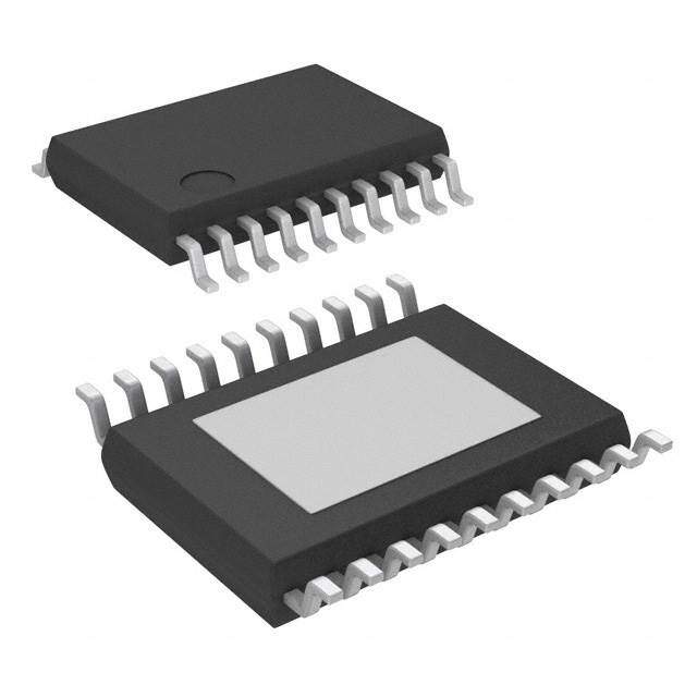
| 描述 | IC OPAMP GP 10MHZ 20HTSSOP运算放大器 - 运放 Quad High-Output |
| 产品分类 | Linear - Amplifiers - Instrumentation, OP Amps, Buffer Amps集成电路 - IC |
| 品牌 | Texas Instruments |
| 产品手册 | |
| 产品图片 |
|
| rohs | 符合RoHS无铅 / 符合限制有害物质指令(RoHS)规范要求 |
| 产品系列 | 放大器 IC,运算放大器 - 运放,Texas Instruments TLC075IPWP- |
| 数据手册 | |
| 产品型号 | TLC075IPWP |
| 产品目录页面 | |
| 产品种类 | 运算放大器 - 运放 |
| 供应商器件封装 | 20-HTSSOP |
| 共模抑制比—最小值 | 80 dB |
| 关闭 | Shutdown |
| 其它名称 | 296-7254-5 |
| 包装 | 管件 |
| 单位重量 | 81.800 mg |
| 压摆率 | 19 V/µs |
| 双重电源电压 | +/- 3 V, +/- 5 V |
| 商标 | Texas Instruments |
| 增益带宽生成 | 10 MHz |
| 增益带宽积 | 10MHz |
| 安装类型 | 表面贴装 |
| 安装风格 | SMD/SMT |
| 封装 | Tube |
| 封装/外壳 | 20-TSSOP(0.173",4.40mm 宽)裸焊盘 |
| 封装/箱体 | HTSSOP-20 |
| 工作温度 | -40°C ~ 125°C |
| 工作电源电压 | 4.5 V to 16 V, +/- 2.25 V to +/- 8 V |
| 工厂包装数量 | 70 |
| 技术 | BiCMOS |
| 放大器类型 | 通用 |
| 最大双重电源电压 | +/- 8 V |
| 最大工作温度 | + 125 C |
| 最小双重电源电压 | +/- 2.25 V |
| 最小工作温度 | - 40 C |
| 标准包装 | 70 |
| 电压-电源,单/双 (±) | 4.5 V ~ 16 V, ±2.25 V ~ 8 V |
| 电压-输入失调 | 390µV |
| 电流-电源 | 2.1mA |
| 电流-输入偏置 | 1.5pA |
| 电流-输出/通道 | 57mA |
| 电源电流 | 11.6 mA |
| 电路数 | 4 |
| 系列 | TLC075 |
| 转换速度 | 16 V/us |
| 输入偏压电流—最大 | 50 pA |
| 输入参考电压噪声 | 12 nV |
| 输入补偿电压 | 1.9 mV |
| 输出电流 | 57 mA |
| 输出类型 | - |
| 通道数量 | 4 Channel |


- 商务部:美国ITC正式对集成电路等产品启动337调查
- 曝三星4nm工艺存在良率问题 高通将骁龙8 Gen1或转产台积电
- 太阳诱电将投资9.5亿元在常州建新厂生产MLCC 预计2023年完工
- 英特尔发布欧洲新工厂建设计划 深化IDM 2.0 战略
- 台积电先进制程称霸业界 有大客户加持明年业绩稳了
- 达到5530亿美元!SIA预计今年全球半导体销售额将创下新高
- 英特尔拟将自动驾驶子公司Mobileye上市 估值或超500亿美元
- 三星加码芯片和SET,合并消费电子和移动部门,撤换高东真等 CEO
- 三星电子宣布重大人事变动 还合并消费电子和移动部门
- 海关总署:前11个月进口集成电路产品价值2.52万亿元 增长14.8%


PDF Datasheet 数据手册内容提取
TLC070, TLC071, TLC072, TLC073, TLC074, TLC075, TLC07xA FAMILY OF WIDE-BANDWIDTH HIGH-OUTPUT-DRIVE SINGLE SUPPLY OPERATIONAL AMPLIFIERS SLOS219F − JUNE 1999 − REVISED DECEMBER 2011 (cid:2) Wide Bandwidth...10 MHz (cid:2) High Output Drive Operational Amplifier − IOH...57 mA at VDD − 1.5 V − I ...55 mA at 0.5 V OL (cid:2) High Slew Rate − − SR+...16 V/μs − SR−...19 V/μs + (cid:2) Wide Supply Range...4.5 V to 16 V (cid:2) Supply Current...1.9 mA/Channel (cid:2) Ultralow Power Shutdown Mode I ...125 μA/Channel DD (cid:2) Low Input Noise Voltage...7 nV√Hz (cid:2) Input Offset Voltage...60 μV (cid:2) Ultra-Small Packages − 8 or 10 Pin MSOP (TLC070/1/2/3) description The first members of TI’s new BiMOS general-purpose operational amplifier family are the TLC07x. The BiMOS family concept is simple: provide an upgrade path for BiFET users who are moving away from dual-supply to single-supply systems and demand higher AC and dc performance. With performance rated from 4.5 V to 16 V across commercial (0°C to 70°C) and an extended industrial temperature range (−40°C to 125°C), BiMOS suits a wide range of audio, automotive, industrial and instrumentation applications. Familiar features like offset nulling pins, and new features like MSOP PowerPAD™ packages and shutdown modes, enable higher levels of performance in a variety of applications. Developed in TI’s patented LBC3 BiCMOS process, the new BiMOS amplifiers combine a very high input impedance low-noise CMOS front end with a high-drive bipolar output stage, thus providing the optimum performance features of both. AC performance improvements over the TL07x BiFET predecessors include a bandwidth of 10 MHz (an increase of 300%) and voltage noise of 7 nV/√Hz (an improvement of 60%). DC improvements include a factor of 4 reduction in input offset voltage down to 1.5 mV (maximum) in the standard grade, and a power supply rejection improvement of greater than 40 dB to 130 dB. Added to this list of impressive features is the ability to drive ±50-mA loads comfortably from an ultrasmall-footprint MSOP PowerPAD package, which positions the TLC07x as the ideal high-performance general-purpose operational amplifier family. FAMILY PACKAGE TABLE NNOO.. OOFF PACKAGE TYPES UUNNIIVVEERRSSAALL DDEEVVIICCEE SSHHUUTTDDOOWWNN CHANNELS MSOP PDIP SOIC TSSOP EVM BOARD TLC070 1 8 8 8 — Yes TLC071 1 8 8 8 — TLC072 2 8 8 8 — — Refer to the EVM SSeelleeccttiioonn GGuuiiddee TLC073 2 10 14 14 — Yes ((LLiitt## SSLLOOUU006600)) TLC074 4 — 14 14 20 — TLC075 4 — 16 16 20 Yes Please be aware that an important notice concerning availability, standard warranty, and use in critical applications of TexasInstruments semiconductor products and disclaimers thereto appears at the end of this data sheet. PowerPAD is a trademark of Texas Instruments. All other trademarks are the property of their respective owners. PRODUCTION DATA information is current as of publication date. Copyright © 2000−2011, Texas Instruments Incorporated Products conform to specifications per the terms of Texas Instruments standard warranty. Production processing does not necessarily include testing of all parameters. WWW.TI.COM 1
TLC070, TLC071, TLC072, TLC073, TLC074, TLC075, TLC07xA FAMILY OF WIDE-BANDWIDTH HIGH-OUTPUT-DRIVE SINGLE SUPPLY OPERATIONAL AMPLIFIERS SLOS219F − JUNE 1999 − REVISED DECEMBER 2011 TLC070 and TLC071 AVAILABLE OPTIONS PACKAGED DEVICES TTAA SSMMAALLLL OOUUTTLLIINNEE SSMMAALLLL OOUUTTLLIINNEE PPLLAASSTTIICC DDIIPP SSYYMMBBOOLL (D)† (DGN)† (P) TLC070CD TLC070CDGN xxTIACS TLC070CP 0°C to 70°C TLC071CD TLC071CDGN xxTIACU TLC071CP TLC070ID TLC070IDGN xxTIACT TLC070IP TLC071ID TLC071IDGN xxTIACV TLC071IP −4400°°CC ttoo 112255°°CC TLC070AID — — TLC070AIP TLC071AID — — TLC071AIP †This package is available taped and reeled. To order this packaging option, add an R suffix to the part number (e.g., TLC070CDR). TLC072 and TLC073 AVAILABLE OPTIONS PACKAGED DEVICES TTAA SMALL MSOP PLASTIC PLASTIC OOUUTTLLIINNEE DDIIPP DDIIPP (D)† (DGN)† SYMBOL‡ (DGQ)† SYMBOL‡ (N) (P) TLC072CD TLC072CDGN xxTIADV — — — TLC072CP 0°C to 70°C TLC073CD — — TLC073CDGQ xxTIADX TLC073CN — TLC072ID TLC072IDGN xxTIADW — — — TLC072IP TLC073ID — — TLC073IDGQ xxTIADY TLC073IN — −4400°°CC ttoo 112255°°CC TLC072AID — — — — — TLC072AIP TLC073AID — — — — TLC073AIN — †This package is available taped and reeled. To order this packaging option, add an R suffix to the part number (e.g., TLC072CDR). ‡xx represents the device date code. TLC074 and TLC075 AVAILABLE OPTIONS PACKAGED DEVICES TA SMALL OUTLINE PLASTIC DIP TSSOP (D)† (N) (PWP)† TLC074CD TLC074CN TLC074CPWP 0°C to 70°C TLC075CD TLC075CN TLC075CPWP TLC074ID TLC074IN TLC074IPWP TLC075ID TLC075IN TLC075IPWP −4400°°CC ttoo 112255°°CC TLC074AID TLC074AIN TLC074AIPWP TLC075AID TLC075AIN TLC075AIPWP †This package is available taped and reeled. To order this packaging option, add an R suffix to the part number (e.g., TLC074CDR). 2 WWW.TI.COM
TLC070, TLC071, TLC072, TLC073, TLC074, TLC075, TLC07xA FAMILY OF WIDE-BANDWIDTH HIGH-OUTPUT-DRIVE SINGLE SUPPLY OPERATIONAL AMPLIFIERS SLOS219F − JUNE 1999 − REVISED DECEMBER 2011 TLC07x PACKAGE PIN OUTS TLC070 TLC071 TLC072 D, DGN OR P PACKAGE D, DGN OR P PACKAGE D, DGN, OR P PACKAGE (TOP VIEW) (TOP VIEW) (TOP VIEW) NULL 1 8 SHDN NULL 1 8 NC 1OUT 1 8 VDD IN− 2 7 VDD IN− 2 7 VDD 1IN− 2 7 2OUT IN+ 3 6 OUT IN+ 3 6 OUT 1IN+ 3 6 2IN− GND 4 5 NULL GND 4 5 NULL GND 4 5 2IN+ TLC073 TLC073 TLC074 DGQ PACKAGE D OR N PACKAGE D OR N PACKAGE (TOP VIEW) (TOP VIEW) (TOP VIEW) 11OIUNT− 12 190 V2ODDUT 1OUT 1 14 VDD 1OUT 1 14 4OUT 1IN− 2 13 2OUT 1IN− 2 13 4IN− 1IN+ 3 8 2IN− 1IN+ 3 12 2IN− 1IN+ 3 12 4IN+ GND 4 7 2IN+ 1SHDN 5 6 2SHDN GND 4 11 2IN+ VDD 4 11 GND NC 5 10 NC 2IN+ 5 10 3IN+ 1SHDN 6 9 2SHDN 2IN− 6 9 3IN− NC 7 8 NC 2OUT 7 8 3OUT TLC074 TLC075 TLC075 PWP PACKAGE D OR N PACKAGE PWP PACKAGE (TOP VIEW) (TOP VIEW) (TOP VIEW) 1OUT 1 20 4OUT 1OUT 1 16 4OUT 1OUT 1 20 4OUT 1IN− 2 19 4IN− 1IN− 2 15 4IN− 1IN− 2 19 4IN− 1IN+ 3 18 4IN+ 1IN+ 3 14 4IN+ 1IN+ 3 18 4IN+ VDD 4 17 GND VDD 4 13 GND VDD 4 17 GND 2IN+ 5 16 3IN+ 2IN+ 5 12 3IN+ 2IN+ 5 16 3IN+ 2IN− 6 15 3IN− 2IN− 6 11 3IN− 2IN− 6 15 3IN− 2OUT 7 14 3OUT 2OUT 7 10 3OUT 2OUT 7 14 3OUT NC 8 13 NC 1/2SHDN 8 9 3/4SHDN 1/2SHDN 8 13 3/4SHDN NC 9 12 NC NC 9 12 NC NC 10 11 NC NC 10 11 NC NC − No internal connection TYPICAL PIN 1 INDICATORS Pin 1 Printed or Pin 1 Pin 1 Pin 1 Molded Dot Stripe Bevel Edges Molded ”U” Shape WWW.TI.COM 3
TLC070, TLC071, TLC072, TLC073, TLC074, TLC075, TLC07xA FAMILY OF WIDE-BANDWIDTH HIGH-OUTPUT-DRIVE SINGLE SUPPLY OPERATIONAL AMPLIFIERS SLOS219F − JUNE 1999 − REVISED DECEMBER 2011 absolute maximum ratings over operating free-air temperature range (unless otherwise noted)† Supply voltage, V (see Note 1) . . . . . . . . . . . . . . . . . . . . . . . . . . . . . . . . . . . . . . . . . . . . . . . . . . . . . . . . . . . . 17 V DD Differential input voltage range, V . . . . . . . . . . . . . . . . . . . . . . . . . . . . . . . . . . . . . . . . . . . . . . . . . . . . . . . . . ±V ID DD Continuous total power dissipation . . . . . . . . . . . . . . . . . . . . . . . . . . . . . . . . . . . . . See Dissipation Rating Table Operating free-air temperature range, T : C suffix . . . . . . . . . . . . . . . . . . . . . . . . . . . . . . . . . . . . . . 0°C to 70°C A I suffix . . . . . . . . . . . . . . . . . . . . . . . . . . . . . . . . . . . . −40°C to 125°C Maximum junction temperature, T . . . . . . . . . . . . . . . . . . . . . . . . . . . . . . . . . . . . . . . . . . . . . . . . . . . . . . . . . 150°C J Storage temperature range, T . . . . . . . . . . . . . . . . . . . . . . . . . . . . . . . . . . . . . . . . . . . . . . . . . . . −65°C to 150°C stg Lead temperature 1,6 mm (1/16 inch) from case for 10 seconds . . . . . . . . . . . . . . . . . . . . . . . . . . . . . . . 260°C †Stresses beyond those listed under “absolute maximum ratings” may cause permanent damage to the device. These are stress ratings only, and functional operation of the device at these or any other conditions beyond those indicated under “recommended operating conditions” is not implied. Exposure to absolute-maximum-rated conditions for extended periods may affect device reliability. NOTE 1: All voltage values, except differential voltages, are with respect to GND. DISSIPATION RATING TABLE PACKAGE (°θCJ/CW) (°θCJ/AW) POWTAE R≤ 2R5A°CTING D (8) 38.3 176 710 mW D (14) 26.9 122.3 1022 mW D (16) 25.7 114.7 1090 mW DGN (8) 4.7 52.7 2.37 W DGQ (10) 4.7 52.3 2.39 W N (14, 16) 32 78 1600 mW P (8) 41 104 1200 mW PWP (20) 1.40 26.1 4.79 W recommended operating conditions MIN MAX UNIT Single supply 4.5 16 SSuuppppllyy vvoollttaaggee, VVDD Split supply ±2.25 ±8 VV Common-mode input voltage, VICR +0.5 VDD−0.8 V SShhuuttddoowwnn oonn//ooffff vvoollttaaggee lleevveell‡‡ VIH 2 VV VOL 0.8 C-suffix 0 70 OOppeerraattiinngg ffrreeee-aaiirr tteemmppeerraattuurree, TTA °°CC I-suffix −40 125 ‡Relative to the voltage on the GND terminal of the device. 4 WWW.TI.COM
TLC070, TLC071, TLC072, TLC073, TLC074, TLC075, TLC07xA FAMILY OF WIDE-BANDWIDTH HIGH-OUTPUT-DRIVE SINGLE SUPPLY OPERATIONAL AMPLIFIERS SLOS219F − JUNE 1999 − REVISED DECEMBER 2011 electrical characteristics at specified free-air temperature, V = 5 V (unless otherwise noted) DD PARAMETER TEST CONDITIONS TA† MIN TYP MAX UNIT TTLLCC007700//11//22//33,, 25°C 390 1900 TLC074/5 Full range 3000 VVIO IInnppuutt ooffffsseett vvoollttaaggee VVVVDDIICCDD == == 22 55..55 VV VV,,, TTLLCC007700//11//22//33AA,, 25°C 390 1400 μVV VO = 2.5 V, TLC074/5A Full range 2000 RRS = 5500 ΩΩ TTeemmppeerraattuurree ccooeeffffiicciieenntt ooff iinnppuutt αVIO offset voltage 11.22 μVV//°°CC 25°C 0.7 50 IIIIOO IInnppuutt ooffffsseett ccuurrrreenntt VVDDDD == 55 VV, TLC07XC FFuullll rraannggee 100 ppAA VVIICC == 22..55 VV,, TLC07XI 700 VOO = 2.5 V, 25°C 1.5 50 IIIIBB IInnppuutt bbiiaass ccuurrrreenntt RRS = 5500 ΩΩ TLC07XC 100 ppAA FFuullll rraannggee TLC07XI 700 0.5 25°C to 4.2 VVICR CCoommmmoonn-mmooddee iinnppuutt vvoollttaaggee RRS = 5500 ΩΩ 0.5 VV Full range to 4.2 25°C 4.1 4.3 IIOH = −11 mmAA Full range 3.9 25°C 3.7 4 IIOH = −2200 mmAA Full range 3.5 VOOHH Higgh-level outpput voltagge VIICC = 2.5 V 25°C 3.4 3.8 V IIOH = −3355 mmAA Full range 3.2 25°C 3.2 3.6 IOH = −50 mA −40°C to 85°C 3 25°C 0.18 0.25 IIOL = 11 mmAA Full range 0.35 25°C 0.35 0.39 IIOL = 2200 mmAA Full range 0.45 VOOLL Low-level outpput voltagge VIICC = 2.5 V 25°C 0.43 0.55 V IIOL = 3355 mmAA Full range 0.7 25°C 0.48 0.63 IOL = 50 mA −40°C to 85°C 0.7 Sourcing 25°C 100 IIOS SShhoorrtt-cciirrccuuiitt oouuttppuutt ccuurrrreenntt Sinking 25°C 100 mmAA VOH = 1.5 V from positive rail 25°C 57 IIO OOuuttppuutt ccuurrrreenntt VOL = 0.5 V from negative rail 25°C 55 mmAA †Full range is 0°C to 70°C for C suffix and −40°C to 125°C for I suffix. If not specified, full range is −40°C to 125°C. WWW.TI.COM 5
TLC070, TLC071, TLC072, TLC073, TLC074, TLC075, TLC07xA FAMILY OF WIDE-BANDWIDTH HIGH-OUTPUT-DRIVE SINGLE SUPPLY OPERATIONAL AMPLIFIERS SLOS219F − JUNE 1999 − REVISED DECEMBER 2011 electrical characteristics at specified free-air temperature, V = 5 V (unless otherwise noted) DD (continued) PARAMETER TEST CONDITIONS TA† MIN TYP MAX UNIT LLaarrggee-ssiiggnnaall ddiiffffeerreennttiiaall vvoollttaaggee 25°C 100 120 AAVD amplification VVO(PP) = 33 VV, RRL = 1100 kkΩΩ Full range 100 ddBB ri(d) Differential input resistance 25°C 1000 GΩ Common-mode input CIC capacitance f = 10 kHz 25°C 22.9 pF zo Closed-loop output impedance f = 10 kHz, AV = 10 25°C 0.25 Ω 25°C 80 95 CCMMRRRR CCoommmmoonn-mmooddee rreejjeeccttiioonn rraattiioo VVIC = 11 ttoo 33 VV, RRS = 5500ΩΩ Full range 80 ddBB kkSVR SS(ΔuuVppDppDllyy /vvΔooVllttIaaOgg)ee rreejjeeccttiioonn rraattiioo VVNDDoDD lo ==a d44..55 VV ttoo 1166 VV,, VVIICC == VVDDDD//22,, Fu2ll 5r°aCnge 8800 100 ddBB 25°C 1.9 2.5 IIDD SSuuppppllyy ccuurrrreenntt ((ppeerr cchhaannnneell)) VVO = 22.55 VV, NNoo llooaadd mmAA Full range 3.5 Supply current in shutdown 25°C 125 200 IIDD(SHDN) mmooddee ((ppeerr cchhaannnneell)) SSHHDDNN ≤≤ 00.88 VV μAA (TLC070, TLC073, TLC075) Full range 250 †Full range is 0°C to 70°C for C suffix and −40°C to 125°C for I suffix. If not specified, full range is −40°C to 125°C. 6 WWW.TI.COM
TLC070, TLC071, TLC072, TLC073, TLC074, TLC075, TLC07xA FAMILY OF WIDE-BANDWIDTH HIGH-OUTPUT-DRIVE SINGLE SUPPLY OPERATIONAL AMPLIFIERS SLOS219F − JUNE 1999 − REVISED DECEMBER 2011 operating characteristics at specified free-air temperature, V = 5 V (unless otherwise noted) DD PARAMETER TEST CONDITIONS TA† MIN TYP MAX UNIT SSRR+ PPoossiittiivvee sslleeww rraattee aatt uunniittyy ggaaiinn VVROOL ((=PP PP1))0 == k 00Ω..88 VV,, CCLL == 5500 ppFF,, Fu2ll 5r°aCnge 91.05 16 VV//μss SSRR− NNeeggaattiivvee sslleeww rraattee aatt uunniittyy ggaaiinn VVROOL ((=PP PP1))0 == k 00Ω..88 VV,, CCLL == 5500 ppFF,, Fu2ll 5r°aCnge 121.05 19 VV//μss f = 100 Hz 25°C 12 VVn EEqquuiivvaalleenntt iinnppuutt nnooiissee vvoollttaaggee f = 1 kHz 25°C 7 nnVV//√√HHzz In Equivalent input noise current f = 1 kHz 25°C 0.6 fA/√Hz VVOO((PPPP)) == 33 VV,, AV = 1 0.002% TTHHDD ++ NN TToottaall hhaarrmmoonniicc ddiissttoorrttiioonn pplluuss nnooiissee RRLL = 1100 kkΩΩ aanndd 225500 ΩΩ,, AV = 10 2255°CC 0.012% f = 1 kHz AV = 100 0.085% tt((oofnf)) AAmmpplliiffiieerr ttuurrnn--oonff ttiimmee‡‡ RRL = 1100 kkΩΩ 2255°°CC 01.1.35 μμss Gain-bandwidth product f = 10 kHz, RL = 10 kΩ 25°C 10 MHz V(STEP)PP = 1 V, 0.1% 0.18 AAVV == −−11,, tts SSeettttlliinngg ttiimmee RCLL == 1100 pkΩF, 0.01% 2255°°CC 0.39 μss V(STEP)PP = 1 V, 0.1% 0.18 AAVV == −−11,, RCLL == 4170 pkΩF, 0.01% 0.39 RL = 10 kΩ, CL = 50 pF 32° φφm PPhhaassee mmaarrggiinn RL = 10 kΩ, CL = 0 pF 2255°°CC 40° RL = 10 kΩ, CL = 50 pF 2.2 GGaaiinn mmaarrggiinn 2255°°CC ddBB RL = 10 kΩ, CL = 0 pF 3.3 †Full range is 0°C to 70°C for C suffix and −40°C to 125°C for I suffix. If not specified, full range is −40°C to 125°C. ‡Disable time and enable time are defined as the interval between application of the logic signal to SHDN and the point at which the supply current has reached half its final value. WWW.TI.COM 7
TLC070, TLC071, TLC072, TLC073, TLC074, TLC075, TLC07xA FAMILY OF WIDE-BANDWIDTH HIGH-OUTPUT-DRIVE SINGLE SUPPLY OPERATIONAL AMPLIFIERS SLOS219F − JUNE 1999 − REVISED DECEMBER 2011 electrical characteristics at specified free-air temperature, V = 12 V (unless otherwise noted) DD PARAMETER TEST CONDITIONS TA† MIN TYP MAX UNIT TTLLCC007700//11//22//33,, 25°C 390 1900 TLC074/5 Full range 3000 VVIO IInnppuutt ooffffsseett vvoollttaaggee VVVVDDIICCDD == == 66 11 VV22,, VV TTLLCC007700//11//22//33AA,, 25°C 390 1400 μVV VO = 6 V, TLC074/5A Full range 2000 RRS = 5500 ΩΩ TTeemmppeerraattuurree ccooeeffffiicciieenntt ooff iinnppuutt αVIO offset voltage 11.22 μVV//°°CC 25°C 0.7 50 IIIIOO IInnppuutt ooffffsseett ccuurrrreenntt VVDDDD == 1122 VV TLC07xC FFuullll rraannggee 100 ppAA VVIICC == 66 VV,, TLC07xI 700 VOO = 6 V, 25°C 1.5 50 IIIIBB IInnppuutt bbiiaass ccuurrrreenntt RRS = 5500 ΩΩ TLC07xC 100 ppAA FFuullll rraannggee TLC07xI 700 0.5 25°C to 11.2 VVICR CCoommmmoonn-mmooddee iinnppuutt vvoollttaaggee RRS = 5500 ΩΩ 0.5 VV Full range to 11.2 25°C 11.1 11.2 IIOH = −11 mmAA Full range 11 25°C 10.8 10.9 IIOH = −2200 mmAA Full range 10.7 VOOHH Higgh-level outpput voltagge VIICC = 6 V 25°C 10.6 10.7 V IIOH = −3355 mmAA Full range 10.3 25°C 10.4 10.5 IOH = −50 mA −40°C to 85°C 10.3 25°C 0.17 0.25 IIOL = 11 mmAA Full range 0.35 25°C 0.35 0.45 IIOL = 2200 mmAA Full range 0.5 VOOLL Low-level outpput voltagge VIICC = 6 V 25°C 0.4 0.52 V IIOL = 3355 mmAA Full range 0.6 25°C 0.45 0.6 IOL = 50 mA −40°C to 85°C 0.65 Sourcing 25°C 150 IIOS SShhoorrtt-cciirrccuuiitt oouuttppuutt ccuurrrreenntt Sinking 25°C 150 mmAA VOH = 1.5 V from positive rail 25°C 57 IIO OOuuttppuutt ccuurrrreenntt VOL = 0.5 V from negative rail 25°C 55 mmAA †Full range is 0°C to 70°C for C suffix and −40°C to 125°C for I suffix. If not specified, full range is −40°C to 125°C. 8 WWW.TI.COM
TLC070, TLC071, TLC072, TLC073, TLC074, TLC075, TLC07xA FAMILY OF WIDE-BANDWIDTH HIGH-OUTPUT-DRIVE SINGLE SUPPLY OPERATIONAL AMPLIFIERS SLOS219F − JUNE 1999 − REVISED DECEMBER 2011 electrical characteristics at specified free-air temperature, V = 12 V (unless otherwise noted) DD (continued) PARAMETER TEST CONDITIONS TA† MIN TYP MAX UNIT LLaarrggee-ssiiggnnaall ddiiffffeerreennttiiaall vvoollttaaggee 25°C 120 140 AAVD amplification VVO(PP) = 88 VV, RRL = 1100 kkΩΩ Full range 120 ddBB ri(d) Differential input resistance 25°C 1000 GΩ Common-mode input CIC capacitance f = 10 kHz 25°C 21.6 pF zo Closed-loop output impedance f = 10 kHz, AV = 10 25°C 0.25 Ω 25°C 80 100 CCMMRRRR CCoommmmoonn-mmooddee rreejjeeccttiioonn rraattiioo VVIC = 11 ttoo 1100 VV, RRS = 5500ΩΩ Full range 80 ddBB kkSVR SS(ΔuuVppDppDllyy /vvΔooVllttIaaOgg)ee rreejjeeccttiioonn rraattiioo VVNDDoDD lo ==a d44..55 VV ttoo 1166 VV,, VVIICC == VVDDDD//22,, Fu2ll 5r°aCnge 8800 100 ddBB 25°C 2.1 2.9 IIDD SSuuppppllyy ccuurrrreenntt ((ppeerr cchhaannnneell)) VVO = 77.55 VV, NNoo llooaadd mmAA Full range 3.5 Supply current in shutdown 25°C 125 200 IIDD(SHDN) mmooddee ((TTLLCC007700, TTLLCC007733, SSHHDDNN ≤≤ 00.88 VV μAA TLC075) (per channel) Full range 250 †Full range is 0°C to 70°C for C suffix and −40°C to 125°C for I suffix. If not specified, full range is −40°C to 125°C. WWW.TI.COM 9
TLC070, TLC071, TLC072, TLC073, TLC074, TLC075, TLC07xA FAMILY OF WIDE-BANDWIDTH HIGH-OUTPUT-DRIVE SINGLE SUPPLY OPERATIONAL AMPLIFIERS SLOS219F − JUNE 1999 − REVISED DECEMBER 2011 operating characteristics at specified free-air temperature, V = 12 V (unless otherwise noted) DD PARAMETER TEST CONDITIONS TA† MIN TYP MAX UNIT SSRR+ PPoossiittiivvee sslleeww rraattee aatt uunniittyy ggaaiinn VVROOL ((=PP PP1))0 == k 22Ω VV,, CCLL == 5500 ppFF,, Fu2ll 5r°aCnge 91.05 16 VV//μss SSRR− NNeeggaattiivvee sslleeww rraattee aatt uunniittyy ggaaiinn VVROOL ((=PP PP1))0 == k 22Ω VV,, CCLL == 5500 ppFF,, Fu2ll 5r°aCnge 121.05 19 VV//μss f = 100 Hz 25°C 12 VVn EEqquuiivvaalleenntt iinnppuutt nnooiissee vvoollttaaggee f = 1 kHz 25°C 7 nnVV//√√HHzz In Equivalent input noise current f = 1 kHz 25°C 0.6 fA/√Hz VVOO((PPPP)) == 88 VV,, AV = 1 0.002% TTHHDD ++ NN TToottaall hhaarrmmoonniicc ddiissttoorrttiioonn pplluuss nnooiissee RRLL = 1100 kkΩΩ aanndd 225500 ΩΩ,, AV = 10 2255°CC 0.005% f = 1 kHz AV = 100 0.022% tt((oofnf)) AAmmpplliiffiieerr ttuurrnn--oonff ttiimmee‡‡ RRL = 1100 kkΩΩ 2255°°CC 02.4.57 μμss Gain-bandwidth product f = 10 kHz, RL = 10 kΩ 25°C 10 MHz V(STEP)PP = 1 V, 0.1% 0.17 AAVV == −−11,, tts SSeettttlliinngg ttiimmee CRLL == 1100 pkΩF, 0.01% 2255°°CC 0.22 μss V(STEP)PP = 1 V, 0.1% 0.17 AAVV == −−11,, CRLL == 4170 pkΩF, 0.01% 0.29 RL = 10 kΩ, CL = 50 pF 37° φφm PPhhaassee mmaarrggiinn RL = 10 kΩ, CL = 0 pF 2255°°CC 42° RL = 10 kΩ, CL = 50 pF 3.1 GGaaiinn mmaarrggiinn 2255°°CC ddBB RL = 10 kΩ, CL = 0 pF 4 †Full range is 0°C to 70°C for C suffix and −40°C to 125°C for I suffix. If not specified, full range is −40°C to 125°C. ‡Disable time and enable time are defined as the interval between application of the logic signal to SHDN and the point at which the supply current has reached half its final value. 10 WWW.TI.COM
TLC070, TLC071, TLC072, TLC073, TLC074, TLC075, TLC07xA FAMILY OF WIDE-BANDWIDTH HIGH-OUTPUT-DRIVE SINGLE SUPPLY OPERATIONAL AMPLIFIERS SLOS219F − JUNE 1999 − REVISED DECEMBER 2011 TYPICAL CHARACTERISTICS Table of Graphs FIGURE VIO Input offset voltage vs Common-mode input voltage 1, 2 IIO Input offset current vs Free-air temperature 3, 4 IIB Input bias current vs Free-air temperature 3, 4 VOH High-level output voltage vs High-level output current 5, 7 VOL Low-level output voltage vs Low-level output current 6, 8 Zo Output impedance vs Frequency 9 IDD Supply current vs Supply voltage 10 PSRR Power supply rejection ratio vs Frequency 11 CMRR Common-mode rejection ratio vs Frequency 12 Vn Equivalent input noise voltage vs Frequency 13 VO(PP) Peak-to-peak output voltage vs Frequency 14, 15 Crosstalk vs Frequency 16 Differential voltage gain vs Frequency 17, 18 Phase vs Frequency 17, 18 φm Phase margin vs Load capacitance 19, 20 Gain margin vs Load capacitance 21, 22 Gain-bandwidth product vs Supply voltage 23 vs Supply voltage 24 SR Slew rate vs Free-air temperature 25, 26 vs Frequency 27, 28 TTHHDD + NN TToottaall hhaarrmmoonniicc ddiissttoorrttiioonn pplluuss nnooiissee vs Peak-to-peak output voltage 29, 30 Large-signal follower pulse response 31, 32 Small-signal follower pulse response 33 Large-signal inverting pulse response 34, 35 Small-signal inverting pulse response 36 Shutdown forward isolation vs Frequency 37, 38 Shutdown reverse isolation vs Frequency 39, 40 vs Supply voltage 41 SShhuuttddoowwnn ssuuppppllyy ccuurrrreenntt vs Free-air temperature 42 Shutdown pulse 43, 44 WWW.TI.COM 11
TLC070, TLC071, TLC072, TLC073, TLC074, TLC075, TLC07xA FAMILY OF WIDE-BANDWIDTH HIGH-OUTPUT-DRIVE SINGLE SUPPLY OPERATIONAL AMPLIFIERS SLOS219F − JUNE 1999 − REVISED DECEMBER 2011 TYPICAL CHARACTERISTICS INPUT BIAS CURRENT AND INPUT OFFSET VOLTAGE INPUT OFFSET VOLTAGE INPUT OFFSET CURRENT vs vs vs COMMON-MODE INPUT VOLTAGE COMMON-MODE INPUT VOLTAGE A FREE-AIR TEMPERATURE p 250 0 − 20 μV− Input Offset Voltage −VIO 112211570207225050505550 VTAD D= 2=5 °5 C V μV− Input Offset Voltage −VIO−−−−−−−−−111221570275202050550505 VTAD D= 2=5 1° 2C V Input Bias and Input Offset Current − −−−−−124608000000 VDD = 5V IIBIIO 0 −250 O I −25 −275 I/B−120 0.0 0.5 1.0 1.5 2.0 2.5 3.0 3.5 4.0 4.5 5.0 0 1 2 3 4 5 6 7 8 9 10 11 12 II −55−40−25−10 5 20 35 50 6580 95110125 VICR − Common-Mode Input Voltage − V VICR − Common-Mode Input Voltage − V TA − Free−Air Temperature − °C Figure 1 Figure 2 Figure 3 INPUT BIAS CURRENT AND HIGH-LEVEL OUTPUT VOLTAGE LOW-LEVEL OUTPUT VOLTAGE INPUT OFFSET CURRENT vs vs vs A HIGH-LEVEL OUTPUT CURRENT LOW-LEVEL OUTPUT CURRENT p FREE-AIR TEMPERATURE Input Bias and Input Offset Current − −O−−−−−−−11122246048000000000 VDD = 12 V IIIBIO V− High-Level Output Voltage − VOH 233445......505050 TVAD D= =− 450 V°C TA T=A 7 =0 °1C25°CTA = 25°C V− Low-Level Output Voltage − VOL 0000000001..........1234567890 VDD T=A 5 = V 25T°AC = 70°CTA =T A1 2=5 −°4C0°C I I /B−160 2.0 0.0 II −55−40−25−10 5 20 35 50 6580 95110125 0 5 10 15 20 25 30 35 40 45 50 0 5 10 15 20 25 30 35 40 45 50 TA − Free-Air Temperature − °C IOH - High-Level Output Current - mA IOL - Low-Level Output Current - mA Figure 4 Figure 5 Figure 6 HIGH-LEVEL OUTPUT VOLTAGE LOW-LEVEL OUTPUT VOLTAGE OUTPUT IMPEDANCE vs vs vs HIGH-LEVEL OUTPUT CURRENT LOW-LEVEL OUTPUT CURRENT FREQUENCY 12.0 1.0 1000 V age − 11.5 TA = 125°CTA = 70°C ge − V 00..89 Ω 100 VTAD D= =2 55° VC and 12 V V− High-Level Output VoltOH1110019....0505 VDD = 12T VA = 25°C TA = −40°C V− Low-Level Output VoltaOL 0000000.......1234567 TVAD =D 2=5 1°C2 V TA = T7A0 °=C 12T5A°C = −40°C − Output Impedance −Zo0.11010 AAAVVV === 111000 9.0 0.0 0.01 0 5 10 15 20 25 30 35 40 45 50 0 5 10 15 20 25 30 35 40 45 50 100 1k 10k 100k 1M 10M IOH - High-Level Output Current - mA IOL - Low-Level Output Current - mA f - Frequency - Hz Figure 7 Figure 8 Figure 9 12 WWW.TI.COM
TLC070, TLC071, TLC072, TLC073, TLC074, TLC075, TLC07xA FAMILY OF WIDE-BANDWIDTH HIGH-OUTPUT-DRIVE SINGLE SUPPLY OPERATIONAL AMPLIFIERS SLOS219F − JUNE 1999 − REVISED DECEMBER 2011 TYPICAL CHARACTERISTICS SUPPLY CURRENT POWER SUPPLY REJECTION RATIO COMMON-MODE REJECTION RATIO vs vs vs SUPPLY VOLTAGE FREQUENCY FREQUENCY 3.0 B 140 B 140 − mA 2.5 TA = −40°C TA = 25°C on Ratio − d 112000 VDD = 12 V on Ratio − d 110200 VTAD D= =2 55° CV and 12 V pply Current 12..50 TA = 70°C TA = 125°C upply Rejecti 8600 Mode Rejecti 6800 − SuDD 1.0 Power S 40 VDD = 5 V ommon- 40 I 00..05 ASPVHe r=D C N1h a=n VnDeDl −PSRR 200 CMRR − C 200 4 5 6 7 8 9 10 11 12 13 14 15 16 0 10 100 1k 10k 100k 1M 10M 100 1k 10k 100k 1M 10M VDD − Supply Voltage - V f − Frequency − Hz f - Frequency - Hz Figure 10 Figure 11 Figure 12 PEAK-TO-PEAK OUTPUT PEAK-TO-PEAK OUTPUT EQUIVALENT INPUT NOISE VOLTAGE VOLTAGE VOLTAGE vs vs vs FREQUENCY FREQUENCY FREQUENCY Hz 40 V 12 V 12 nV/ 35 VDD = 12 V age − 10 VDD = 12 V age − 10 VDD = 12 V oltage − 2350 put Volt 8 put Volt 8 e V Out Out Nois 20 eak 6 eak 6 quivalent Input 11505 VDD = 5 V − Peak-to-PPP) 24 TRVHLD D=D + 6=N0 5 0< VΩ = 5% − Peak-to-PPP) 24 TRVHL DD=D +1 N=0 5<k Ω V= 5% − En 0 VO( 0 TA = 25°C VO( 0 TA = 25°C V 10 100 1k 10k 100k 10k 100k 1M 10M 10k 100k 1M 10M f − Frequency − Hz f - Frequency - Hz f - Frequency - Hz Figure 13 Figure 14 Figure 15 CROSSTALK vs FREQUENCY 0 VDD = 5 V and 12 V −20 AV = 1 RL = 10 kΩ −40 VI(PP) = 2 V For All Channels −60 B d k − −80 al sst −100 o Cr −120 −140 −160 10 100 1k 10k 100k f − Frequency − Hz Figure 16 WWW.TI.COM 13
TLC070, TLC071, TLC072, TLC073, TLC074, TLC075, TLC07xA FAMILY OF WIDE-BANDWIDTH HIGH-OUTPUT-DRIVE SINGLE SUPPLY OPERATIONAL AMPLIFIERS SLOS219F − JUNE 1999 − REVISED DECEMBER 2011 TYPICAL CHARACTERISTICS DIFFERENTIAL VOLTAGE GAIN AND DIFFERENTIAL VOLTAGE GAIN AND PHASE PHASE vs vs FREQUENCY FREQUENCY 80 0 80 0 B 70 B 70 d d n − 60 Gain −45 n − 60 Gain −45 ai ai G 50 G 50 erent Voltage 243000 Phase −−19305 °Phase − erent Voltage 243000 Phase −−19305 °Phase − Diff 10 Diff 10 −D 0 VDD = ±2.5 V −180 −D 0 VDD = ±6 V −180 AV −10 RCLL == 100 p kFΩ AV −10 CRLL == 100 p kFΩ TA = 25°C TA = 25°C −20 −225 −20 −225 1k 10k 100k 1M 10M 100M 1k 10k 100k 1M 10M 100M f − Frequency − Hz f − Frequency − Hz Figure 17 Figure 18 PHASE MARGIN PHASE MARGIN GAIN MARGIN vs vs vs LOAD CAPACITANCE LOAD CAPACITANCE LOAD CAPACITANCE 40° 45° 4 35° RRnnuullll == 01 0Ω0 Ω 40° Rnull = 0 Ω 3.5 Rnull = 0 Ω 30° 35° B 3 Rnull = 100 Ω − Phase Marginm 212550°°° Rnull = 50 ΩRnull = 20 Ω − Phase Marginm 23210055°°°° Rnull = 100 Ω Rnull = 50 RΩnull = 20 Ω −Gain Margin − d 21..525 Rnull = 50 Ω φ 105°° VRTADL D== =21 505° kCVΩ φ 105°° VRTADL D== =21 501° 2kC ΩV G 0.15 VRTADL D== =21 505° kCVΩ Rnull = 20 Ω 0° 0° 0 10 100 10 100 10 100 CL − Load Capacitance − pF CL − Load Capacitance − pF CL − Load Capacitance − pF Figure 19 Figure 20 Figure 21 GAIN MARGIN GAIN BANDWIDTH PRODUCT SLEW RATE vs vs vs LOAD CAPACITANCE SUPPLY VOLTAGE SUPPLY VOLTAGE 5 Rnull = 0 Ω 10.0 22 B 4.45 Rnull = 100 Ω ct - MHz 99..89 CTLA == 1215 °pCF 2201 RCAVLL === 651000 p ΩF and 10 kΩ φ− Phase Margin − dm 321...123555 VRDRL Dn= u =1ll 0=1 2 k5 ΩV0 Ω Rnull = 20 Ω P - Gain Bandwidth Produ 999999......234567 RL = 600 Ω RL = 10 kΩ μSR − Slew Rate − V/s 111111456789 SlewS Rleawte R −ate + 0.5 TA = 25°C BW 9.1 13 G 0 9.0 12 10 100 4 5 6 7 8 9 10 11 12 13 14 15 16 4 5 6 7 8 9 10 11 12 13 14 15 16 CL − Load Capacitance − pF VDD - Supply Voltage - V VDD - Supply Voltage - V Figure 22 Figure 23 Figure 24 14 WWW.TI.COM
TLC070, TLC071, TLC072, TLC073, TLC074, TLC075, TLC07xA FAMILY OF WIDE-BANDWIDTH HIGH-OUTPUT-DRIVE SINGLE SUPPLY OPERATIONAL AMPLIFIERS SLOS219F − JUNE 1999 − REVISED DECEMBER 2011 TYPICAL CHARACTERISTICS TOTAL HARMONIC DISTORTION SLEW RATE SLEW RATE PLUS NOISE vs vs vs FREE-AIR TEMPERATURE FREE-AIR TEMPERATURE FREQUENCY 25 25 1 s 20 Slew Rate − VRCADVLL D=== =651 0050 pV ΩF and 10 kΩ s 20 Slew Rate − Noise − % VRVDOL D(=P P=1) 0 5= k V2Ω V μ− Slew Rate − V/ 1105 Slew Rate + μ− Slew Rate − V/ 1105 Slew Rate + monic Distortion + 00.0.11 AAVV == 11000 SR 5 SR 5 VRCDLL D== =65 0010 2p ΩFV and 10 kΩ otal Har AV = 1 AV = 1 T 0 0 0.001 −55 −35 −15 5 25 45 65 85 105 125 −55 −35 −15 5 25 45 65 85 105 125 100 1k 10k 100k TA - Free-Air Temperature - °C TA - Free-Air Temperature - °C f − Frequency − Hz Figure 25 Figure 26 Figure 27 TOTAL HARMONIC DISTORTION TOTAL HARMONIC DISTORTION TOTAL HARMONIC DISTORTION PLUS NOISE PLUS NOISE PLUS NOISE vs vs vs FREQUENCY PEAK-TO-PEAK OUTPUT VOLTAGE PEAK-TO-PEAK OUTPUT VOLTAGE Total Harmonic Distortion + Noise − % 0.00.11 AAAVVV === 111000 VRVDOL D(=P P=1) 0 1= 2k 1 ΩV2 V Total Harmonic Distortion + Noise − % 0.00.0100.01111 VAf =DV D1= k1=H z5 V RL = 600 ΩRLR =L 2=5 100 Ω kΩ Total Harmonic Distortion + Noise − % 0.00.0100.01111 VAf =DV D1= k=1H 1z2 V RL = 600R RΩL L= = 2 1500 kΩΩ 0.001 0.0001 0.0001 100 1k 10k 100k 0.25 0.75 1.25 1.75 2.25 2.75 3.25 3.75 0.5 2.5 4.5 6.5 8.5 10.5 f − Frequency − Hz VO(PP) − Peak-to-Peak Output Voltage − V VO(PP) − Peak-to-Peak Output Voltage − V Figure 28 Figure 29 Figure 30 LARGE SIGNAL FOLLOWER LARGE SIGNAL FOLLOWER SMALL SIGNAL FOLLOWER PULSE PULSE RESPONSE PULSE RESPONSE RESPONSE VI (1 V/Div) VI (5 V/Div) VI(100mV/Div) − Output Voltage − VVO VV RO DLa ( Dn=5 d0 =6 0 105 0m0 V kVΩΩ/Div) − Output Voltage − VVO VO VR ( 2 DLa VDn= /d =D6 10i1v002) kΩVΩ V− Output Voltage − VO VRDL D= V =6O 05(05 V 0Ω ma naVdn/D d1 i12v0 )V kΩ CTAL == 285 p°FC CTAL == 285 p°FC TCAL == 285 p°FC 0 0.2 0.4 0.6 0.8 1 1.2 1.4 1.6 1.8 2 0 0.2 0.4 0.6 0.8 1 1.2 1.4 1.6 1.8 2 0 0.1 0.2 0.3 0.4 0.50.60.7 0.8 0.90.10 t − Time − μs t − Time − μs t − Time − μs Figure 31 Figure 32 Figure 33 WWW.TI.COM 15
TLC070, TLC071, TLC072, TLC073, TLC074, TLC075, TLC07xA FAMILY OF WIDE-BANDWIDTH HIGH-OUTPUT-DRIVE SINGLE SUPPLY OPERATIONAL AMPLIFIERS SLOS219F − JUNE 1999 − REVISED DECEMBER 2011 TYPICAL CHARACTERISTICS LARGE SIGNAL INVERTING LARGE SIGNAL INVERTING SMALL SIGNAL INVERTING PULSE RESPONSE PULSE RESPONSE PULSE RESPONSE VI (2 V/div) VI (5 V/div) VI (100 mV/div) − Output Voltage − VO VRT C A DLLa D=n== d =268 150 5p0°0 FCV kΩΩ − Output Voltage − VO VR CT A DLL a D===n =d268 50 11p°020FC ΩVkΩ − Output Voltage − VO CTVRADLL D=== =268 50 5p°0 FC& Ω 1 a2n Vd 10 kΩ V V V VO (50 mV/Div) VO (500 mV/Div) VO (2 V/Div) 0 0.2 0.4 0.6 0.8 1 1.2 1.4 1.6 1.8 2 0 0.2 0.4 0.6 0.8 1 1.2 1.4 1.6 1.8 2 0 0.1 0.2 0.3 0.4 0.5 0.6 0.7 0.8 0.9 1 t − Time − μs t − Time − μs t − Time − μs Figure 34 Figure 35 Figure 36 SHUTDOWN FORWARD SHUTDOWN FORWARD SHUTDOWN REVERSE ISOLATION ISOLATION ISOLATION vs vs vs FREQUENCY FREQUENCY FREQUENCY 140 140 140 orward Isolation - dB 11028000 TVCVADIL( P=D=P 0=2)R =5p5L° F 0CV=. 16,0 20. 5Ω, and 5 V orward Isolation - dB 11028000 VCTVADIL( P=D=P 0=2) =5p1°R F20CL .V1 =, 86,0 a0n Ωd 12 V verse Isolation - dB 11028000 VCTVADIL( P=D=P 0=2) =5p5° F 0CVR.1L, 2=. 56,0 a0n Ωd 5 V F F e wn 60 wn 60 RL = 10 kΩ n R 60 do RL = 10 kΩ do ow RL = 10 kΩ Sut 40 Sut 40 utd 40 S 20 20 20 100 1k 10k 100k 1M 10M 100M 100 1k 10k 100k 1M 10M 100M 100 1k 10k 100k 1M 10M 100M f - Frequency - Hz f - Frequency - Hz f - Frequency - Hz Figure 37 Figure 38 Figure 39 SHUTDOWN REVERSE ISOLATION SHUTDOWN SUPPLY CURRENT SHUTDOWN SUPPLY CURRENT vs vs vs FREQUENCY SUPPLY VOLTAGE FREE-AIR TEMPERATURE 140 A 136 A 180 Reverse Isolation - dB 11028000 VCTVADIL( P=D=P 0=2) =5p1R° F20CL . V1=, 680, 0a nΩd 12 V μutdown Supply Current - 111112233368024 SRVhILN u= t= do oVpwDenDn /O2n μutdown Supply Current - 111246000 AVVVIND =D= 1=V D1D2/ 2V VDD = 5 V Sutdown 4600 RL = 10 kΩ − ShHDN)111222024 − ShHDN)10800 S S D( D( 20 D118 D 60 100 1k 10k 100k 1M 10M 100M I 4 5 6 7 8 9 10 11 12 13 14 15 16 I −55 −25 5 35 65 95 125 f - Frequency - Hz VDD - Supply Voltage - V TA - Free-Air Temperature - °C Figure 40 Figure 41 Figure 42 16 WWW.TI.COM
TLC070, TLC071, TLC072, TLC073, TLC074, TLC075, TLC07xA FAMILY OF WIDE-BANDWIDTH HIGH-OUTPUT-DRIVE SINGLE SUPPLY OPERATIONAL AMPLIFIERS SLOS219F − JUNE 1999 − REVISED DECEMBER 2011 TYPICAL CHARACTERISTICS SHUTDOWN PULSE SHUTDOWN PULSE 6.0 6 6.0 6 5.5 SD Off 5.5 SD Off A 5.0 Shutdown Pulse 4 A 5.0 Shutdown Pulse 4 m m − 4.5 − 4.5 − Supply Current 22334.....05050 TVCIADDL =DD= 8R=2 5Lp5 °F =CV 10 kΩ −202hutdown Pulse - V − Supply Current 22334.....05050 TVCIADDL =DD= 8R=2 5Lp1 °F2=C V10 kΩ −202hutdown Pulse - V D 1.5 S D 1.5 S ID 1.0 IDD RL = 600 Ω −4 ID 1.0 IDD RL = 600 Ω −4 0.5 0.5 0.0 −6 0.0 −6 0 10 20 30 40 50 60 70 80 0 10 20 30 40 50 60 70 80 t - Time - μs t - Time - μs Figure 43 Figure 44 PARAMETER MEASUREMENT INFORMATION _ Rnull + RL CL Figure 45 APPLICATION INFORMATION input offset voltage null circuit The TLC070 and TLC071 has an input offset nulling function. Refer to Figure 46 for the diagram. IN− − OUT N2 IN+ + N1 100 kΩ R1 VDD− NOTE A: R1 = 5.6 kΩ for offset voltage adjustment of ±10 mV. R1 = 20 kΩ for offset voltage adjustment of ±3 mV. Figure 46. Input Offset Voltage Null Circuit WWW.TI.COM 17
TLC070, TLC071, TLC072, TLC073, TLC074, TLC075, TLC07xA FAMILY OF WIDE-BANDWIDTH HIGH-OUTPUT-DRIVE SINGLE SUPPLY OPERATIONAL AMPLIFIERS SLOS219F − JUNE 1999 − REVISED DECEMBER 2011 APPLICATION INFORMATION driving a capacitive load When the amplifier is configured in this manner, capacitive loading directly on the output will decrease the device’s phase margin leading to high frequency ringing or oscillations. Therefore, for capacitive loads of greater than 10 pF, it is recommended that a resistor be placed in series (R ) with the output of the amplifier, as NULL shown in Figure 47. A minimum value of 20 Ω should work well for most applications. RF RG Input _ RNULL Output + CLOAD Figure 47. Driving a Capacitive Load offset voltage The output offset voltage, (V ) is the sum of the input offset voltage (V ) and both input bias currents (I ) times OO IO IB the corresponding gains. The following schematic and formula can be used to calculate the output offset voltage: RF IIB− RG + − VI VO + RS (cid:3) IIB+(cid:5) (cid:3) (cid:5) (cid:3) (cid:5) (cid:3) (cid:5) R R VOO(cid:2)VIO 1(cid:4) RF (cid:6)IIB(cid:4)RS 1(cid:4) RF (cid:6)IIB–RF G G Figure 48. Output Offset Voltage Model 18 WWW.TI.COM
TLC070, TLC071, TLC072, TLC073, TLC074, TLC075, TLC07xA FAMILY OF WIDE-BANDWIDTH HIGH-OUTPUT-DRIVE SINGLE SUPPLY OPERATIONAL AMPLIFIERS SLOS219F − JUNE 1999 − REVISED DECEMBER 2011 APPLICATION INFORMATION high speed CMOS input amplifiers The TLC07x is a family of high-speed low-noise CMOS input operational amplifiers that has an input capacitance of the order of 20 pF. Any resistor used in the feedback path adds a pole in the transfer function equivalent to the input capacitance multiplied by the combination of source resistance and feedback resistance. For example, a gain of −10, a source resistance of 1 kΩ, and a feedback resistance of 10 kΩ add an additional pole at approximately 8 MHz. This is more apparent with CMOS amplifiers than bipolar amplifiers due to their greater input capacitance. This is of little consequence on slower CMOS amplifiers, as this pole normally occurs at frequencies above their unity-gain bandwidth. However, the TLC07x with its 10-MHz bandwidth means that this pole normally occurs at frequencies where there is on the order of 5 dB gain left and the phase shift adds considerably. The effect of this pole is the strongest with large feedback resistances at small closed loop gains. As the feedback resistance is increased, the gain peaking increases at a lower frequency and the 180(cid:3) phase shift crossover point also moves down in frequency, decreasing the phase margin. For the TLC07x, the maximum feedback resistor recommended is 5 kΩ; larger resistances can be used but a capacitor in parallel with the feedback resistor is recommended to counter the effects of the input capacitance pole. The TLC073 with a 1-V step response has an 80% overshoot with a natural frequency of 3.5 MHz when configured as a unity gain buffer and with a 10-kΩ feedback resistor. By adding a 10-pF capacitor in parallel with the feedback resistor, the overshoot is reduced to 40% and eliminates the natural frequency, resulting in a much faster settling time (see Figure 49). The 10-pF capacitor was chosen for convenience only. Load capacitance had little effect on these measurements due to the excellent output drive capability of the TLC07x. V 2 e − VIN ag 10 pF 1 olt V With 0 nput 10 kΩ − V 1.5 CF = 10 pF −1 − I ge VI _ a olt 1 V + ut IN V− OutpO 0.50 VOUT VARRDVFL D=== =6+1 001±0 5k ΩΩV 50 Ω 600 Ω 22 pF CL = 22 pF −0.5 0 0.2 0.4 0.6 0.8 1 1.2 1.4 1.6 t - Time - μs Figure 49. 1-V Step Response WWW.TI.COM 19
TLC070, TLC071, TLC072, TLC073, TLC074, TLC075, TLC07xA FAMILY OF WIDE-BANDWIDTH HIGH-OUTPUT-DRIVE SINGLE SUPPLY OPERATIONAL AMPLIFIERS SLOS219F − JUNE 1999 − REVISED DECEMBER 2011 APPLICATION INFORMATION general configurations When receiving low-level signals, limiting the bandwidth of the incoming signals into the system is often required. The simplest way to accomplish this is to place an RC filter at the noninverting terminal of the amplifier (see Figure 50). RG RF − + VO VI R1 C1 f (cid:2) 1 –3dB 2(cid:2)R1C1 (cid:3) (cid:5) V R (cid:3) (cid:5) O (cid:2) 1(cid:4) F 1 V R 1(cid:4)sR1C1 I G Figure 50. Single-Pole Low-Pass Filter If even more attenuation is needed, a multiple pole filter is required. The Sallen-Key filter can be used for this task. For best results, the amplifier should have a bandwidth that is 8 to 10 times the filter frequency bandwidth. Failure to do this can result in phase shift of the amplifier. C1 R1 = R2 = R C1 = C2 = C Q = Peaking Factor (Butterworth Q = 0.707) VI + R1 R2 _ f (cid:2) 1 –3dB 2(cid:2)RC C2 RG = RF RF (2 − 1 ) RG Q Figure 51. 2-Pole Low-Pass Sallen-Key Filter 20 WWW.TI.COM
TLC070, TLC071, TLC072, TLC073, TLC074, TLC075, TLC07xA FAMILY OF WIDE-BANDWIDTH HIGH-OUTPUT-DRIVE SINGLE SUPPLY OPERATIONAL AMPLIFIERS SLOS219F − JUNE 1999 − REVISED DECEMBER 2011 APPLICATION INFORMATION shutdown function Three members of the TLC07x family (TLC070/3/5) have a shutdown terminal (SHDN) for conserving battery life in portable applications. When the shutdown terminal is tied low, the supply current is reduced to 125 μA/channel, the amplifier is disabled, and the outputs are placed in a high-impedance mode. To enable the amplifier, the shutdown terminal can either be left floating or pulled high. When the shutdown terminal is left floating, care should be taken to ensure that parasitic leakage current at the shutdown terminal does not inadvertently place the operational amplifier into shutdown. The shutdown terminal threshold is always referenced to the voltage on the GND terminal of the device. Therefore, when operating the device with split supply voltages (e.g. ±2.5 V), the shutdown terminal needs to be pulled to V − (not system ground) to disable DD the operational amplifier. The amplifier’s output with a shutdown pulse is shown in Figures 43 and 44. The amplifier is powered with a single 5-V supply and is configured as noninverting with a gain of 5. The amplifier turn-on and turn-off times are measured from the 50% point of the shutdown pulse to the 50% point of the output waveform. The times for the single, dual, and quad are listed in the data tables. Figures 37, 38, 39, and 40 show the amplifier’s forward and reverse isolation in shutdown. The operational amplifier is configured as a voltage follower (A = 1). The isolation performance is plotted across frequency V using 0.1 V , 2.5 V , and 5 V input signals at ±2.5 V supplies and 0.1 V , 8 V , and 12 V input signals PP PP PP PP PP PP at ±6 V supplies. circuit layout considerations To achieve the levels of high performance of the TLC07x, follow proper printed-circuit board design techniques. A general set of guidelines is given in the following. (cid:2) Ground planes − It is highly recommended that a ground plane be used on the board to provide all components with a low inductive ground connection. However, in the areas of the amplifier inputs and output, the ground plane can be removed to minimize the stray capacitance. (cid:2) Proper power supply decoupling − Use a 6.8-μF tantalum capacitor in parallel with a 0.1-μF ceramic capacitor on each supply terminal. It may be possible to share the tantalum among several amplifiers depending on the application, but a 0.1-μF ceramic capacitor should always be used on the supply terminal of every amplifier. In addition, the 0.1-μF capacitor should be placed as close as possible to the supply terminal. As this distance increases, the inductance in the connecting trace makes the capacitor less effective. The designer should strive for distances of less than 0.1 inches between the device power terminals and the ceramic capacitors. (cid:2) Sockets − Sockets can be used but are not recommended. The additional lead inductance in the socket pins will often lead to stability problems. Surface-mount packages soldered directly to the printed-circuit board is the best implementation. (cid:2) Short trace runs/compact part placements − Optimum high performance is achieved when stray series inductance has been minimized. To realize this, the circuit layout should be made as compact as possible, thereby minimizing the length of all trace runs. Particular attention should be paid to the inverting input of the amplifier. Its length should be kept as short as possible. This will help to minimize stray capacitance at the input of the amplifier. (cid:2) Surface-mount passive components − Using surface-mount passive components is recommended for high performance amplifier circuits for several reasons. First, because of the extremely low lead inductance of surface-mount components, the problem with stray series inductance is greatly reduced. Second, the small size of surface-mount components naturally leads to a more compact layout thereby minimizing both stray inductance and capacitance. If leaded components are used, it is recommended that the lead lengths be kept as short as possible. WWW.TI.COM 21
TLC070, TLC071, TLC072, TLC073, TLC074, TLC075, TLC07xA FAMILY OF WIDE-BANDWIDTH HIGH-OUTPUT-DRIVE SINGLE SUPPLY OPERATIONAL AMPLIFIERS SLOS219F − JUNE 1999 − REVISED DECEMBER 2011 APPLICATION INFORMATION general PowerPAD design considerations The TLC07x is available in a thermally-enhanced PowerPAD family of packages. These packages are constructed using a downset leadframe upon which the die is mounted [see Figure 52(a) and Figure 52(b)]. This arrangement results in the lead frame being exposed as a thermal pad on the underside of the package [see Figure 52(c)]. Because this thermal pad has direct thermal contact with the die, excellent thermal performance can be achieved by providing a good thermal path away from the thermal pad. The PowerPAD package allows for both assembly and thermal management in one manufacturing operation. During the surface-mount solder operation (when the leads are being soldered), the thermal pad must be soldered to a copper area underneath the package. Through the use of thermal paths within this copper area, heat can be conducted away from the package into either a ground plane or other heat dissipating device. Soldering the PowerPAD to the PCB is always required, even with applications that have low-power dissipation. This provides the necessary thermal and mechanical connection between the lead frame die pad and the PCB. The PowerPAD package represents a breakthrough in combining the small area and ease of assembly of surface mount with mechanical methods of heatsinking. DIE Side View (a) Thermal Pad DIE End View (b) Bottom View (c) NOTE A: The thermal pad is electrically isolated from all terminals in the package. Figure 52. Views of Thermally-Enhanced DGN Package 22 WWW.TI.COM
TLC070, TLC071, TLC072, TLC073, TLC074, TLC075, TLC07xA FAMILY OF WIDE-BANDWIDTH HIGH-OUTPUT-DRIVE SINGLE SUPPLY OPERATIONAL AMPLIFIERS SLOS219F − JUNE 1999 − REVISED DECEMBER 2011 APPLICATION INFORMATION Although there are many ways to properly heatsink the PowerPAD package, the following steps illustrate the recommended approach. general PowerPAD design considerations (continued) 1. The thermal pad must be connected to the same voltage potential as the GND pin. 2. Prepare the PCB with a top side etch pattern as illustrated in the thermal land pattern mechanical drawing at the end of this document. There should be etch for the leads as well as etch for the thermal pad. 3. Place five holes (single and dual) or nine holes (quad) in the area of the thermal pad. These holes should be 13 mils in diameter. Keep them small so that solder wicking through the holes is not a problem during reflow. 4. Additional vias may be placed anywhere along the thermal plane outside of the thermal pad area. This helps dissipate the heat generated by the TLC07x IC. These additional vias may be larger than the 13-mil diameter vias directly under the thermal pad. They can be larger because they are not in the thermal pad area to be soldered so that wicking is not a problem. 5. Connect all holes to the internal ground plane that is the same potential as the device GND pin. 6. When connecting these holes to the ground plane, do not use the typical web or spoke via connection methodology. Web connections have a high thermal resistance connection that is useful for slowing the heat transfer during soldering operations. This makes the soldering of vias that have plane connections easier. In this application, however, low thermal resistance is desired for the most efficient heat transfer. Therefore, the holes under the TLC07x PowerPAD package should make their connection to the internal ground plane with a complete connection around the entire circumference of the plated-through hole. 7. The top-side solder mask should leave the terminals of the package and the thermal pad area with its five holes (dual) or nine holes (quad) exposed. The bottom-side solder mask should cover the five or nine holes of the thermal pad area. This prevents solder from being pulled away from the thermal pad area during the reflow process. 8. Apply solder paste to the exposed thermal pad area and all of the IC terminals. 9. With these preparatory steps in place, the TLC07x IC is simply placed in position and run through the solder reflow operation as any standard surface-mount component. This results in a part that is properly installed. For a given θ , the maximum power dissipation is shown in Figure 54 and is calculated by the following formula: JA (cid:3) (cid:5) T –T P (cid:2) MAX A D (cid:2) JA Where: P = Maximum power dissipation of TLC07x IC (watts) D T = Absolute maximum junction temperature (150°C) MAX T = Free-ambient air temperature (°C) A θJA = θJC + θCA θ = Thermal coefficient from junction to case JC θ = Thermal coefficient from case to ambient air (°C/W) CA WWW.TI.COM 23
TLC070, TLC071, TLC072, TLC073, TLC074, TLC075, TLC07xA FAMILY OF WIDE-BANDWIDTH HIGH-OUTPUT-DRIVE SINGLE SUPPLY OPERATIONAL AMPLIFIERS SLOS219F − JUNE 1999 − REVISED DECEMBER 2011 APPLICATION INFORMATION general PowerPAD design considerations (continued) MAXIMUM POWER DISSIPATION vs FREE-AIR TEMPERATURE 7 PWP Package TJ = 150°C Low-K Test PCB 6 θJA = 29.7°C/W W SOT-23 Package ation − 5 DGN Package LθJoAw =-K 3 2T4e°sCt /PWCB p Low-K Test PCB ssi 4 θJA = 52.3°C/W Di SOIC Package er Low-K Test PCB ow 3 θJA = 176°C/W P PDIP Package m Low-K Test PCB mu 2 θJA = 104°C/W xi a M 1 0 −55 −40−25−10 5 20 35 50 65 80 95 110 125 TA − Free-Air Temperature − °C NOTE A: Results are with no air flow and using JEDEC Standard Low-K test PCB. Figure 53. Maximum Power Dissipation vs Free-Air Temperature The next consideration is the package constraints. The two sources of heat within an amplifier are quiescent power and output power. The designer should never forget about the quiescent heat generated within the device, especially multi-amplifier devices. Because these devices have linear output stages (Class A-B), most of the heat dissipation is at low output voltages with high output currents. The other key factor when dealing with power dissipation is how the devices are mounted on the PCB. The PowerPAD devices are extremely useful for heat dissipation. But, the device should always be soldered to a copper plane to fully use the heat dissipation properties of the PowerPAD. The SOIC package, on the other hand, is highly dependent on how it is mounted on the PCB. As more trace and copper area is placed around the device, θ decreases and the heat dissipation capability increases. The currents and voltages shown in JA these graphs are for the total package. For the dual or quad amplifier packages, the sum of the RMS output currents and voltages should be used to choose the proper package. 24 WWW.TI.COM
TLC070, TLC071, TLC072, TLC073, TLC074, TLC075, TLC07xA FAMILY OF WIDE-BANDWIDTH HIGH-OUTPUT-DRIVE SINGLE SUPPLY OPERATIONAL AMPLIFIERS SLOS219F − JUNE 1999 − REVISED DECEMBER 2011 APPLICATION INFORMATION macromodel information Macromodel information provided was derived using MicrosimParts™, the model generation software used with Microsim PSpice™. The Boyle macromodel (see Note 1) and subcircuit in Figure 55 are generated using the TLC07x typical electrical and operating characteristics at T = 25°C. Using this information, output A simulations of the following key parameters can be generated to a tolerance of 20% (in most cases): (cid:2) (cid:2) Maximum positive output voltage swing Unity-gain frequency (cid:2) (cid:2) Maximum negative output voltage swing Common-mode rejection ratio (cid:2) (cid:2) Slew rate Phase margin (cid:2) (cid:2) Quiescent power dissipation DC output resistance (cid:2) (cid:2) Input bias current AC output resistance (cid:2) (cid:2) Open-loop voltage amplification Short-circuit output current limit NOTE 2: G. R. Boyle, B. M. Cohn, D. O. Pederson, and J. E. Solomon, “Macromodeling of Integrated Circuit Operational Amplifiers,” IEEE Journal of Solid-State Circuits, SC-9, 353 (1974). PSpice and Parts are trademarks of MicroSim Corporation. WWW.TI.COM 25
TLC070, TLC071, TLC072, TLC073, TLC074, TLC075, TLC07xA FAMILY OF WIDE-BANDWIDTH HIGH-OUTPUT-DRIVE SINGLE SUPPLY OPERATIONAL AMPLIFIERS SLOS219F − JUNE 1999 − REVISED DECEMBER 2011 APPLICATION INFORMATION 99 DLN 3 EGND + VDD+ 92 9 FB RSS ISS + − 90 91 VB RO2 + DLP + − RP + − HLIM VLP VLN IN− 2 10 VC R2 − − + DP J1 J2 − 6 C2 7 IN+ 53 + 1 VLIM 11 12 DC GCM GA − 8 C1 RD1 RD2 60 RO1 VAD + DE − 54 5 VDD− 4 − + VE OUT *DEVICE=TLC07X_5V, OPAMP, PJF, INT ga 6 0 11 12 457.42E−6 gcm 0 6 10 99 1.1293E−6 * TLC07X − 5V operational amplifier ”macromodel” subcircuit iss 3 10 dc 183.67E−6 * created using Parts release 8.0 on 12/16/99 at 08:38 ioff 0 6 dc .806E−6 * Parts is a MicroSim product. hlim 90 0 vlim 1K * j1 11 2 10 jx1 * connections: non-inverting input j2 12 1 10 jx2 * inverting input r2 6 9 100.00E3 * positive power supply rd1 4 11 2.1862E3 * negative power supply rd2 4 12 2.1862E3 * output ro1 8 5 10 * ro2 7 99 10 rp 3 4 2.4728E3 .subckt TLC07X_5V 1 2 3 4 5 rss 10 99 1.0889E6 * vb 9 0 dc 0 c1 11 12 4.8697E−12 vc 3 53 dc 1.5410 c2 6 7 8.0000E−12 ve 54 4 dc .84403 css 10 99 4.0063E−12 vlim 7 8 dc 0 dc 5 53 dy vlp 91 0 dc 119 de 54 5 dy vln 0 92 dc 119 dlp 90 91 dx .model dx D(Is=800.00E−18) dln 92 90 dx .model dy D(Is=800.00E−18 Rs=1m Cjo=10p) dp 4 3 dx .model jx1 PJF(Is=117.50E−15 Beta=1.1391E−3 Vto=−1) egnd 99 0 poly(2) (3,0) (4,0) 0 .5 .5 .model jx2 PJF(Is=117.50E−15 Beta=1.1391E−3 Vto=−1) fb 7 99 poly(5) vb vc ve vlp vln 0 6.9132E6 −1E3 1E3 .ends 6E6 −6E6 Figure 54. Boyle Macromodel and Subcircuit 26 WWW.TI.COM
PACKAGE OPTION ADDENDUM www.ti.com 6-Feb-2020 PACKAGING INFORMATION Orderable Device Status Package Type Package Pins Package Eco Plan Lead/Ball Finish MSL Peak Temp Op Temp (°C) Device Marking Samples (1) Drawing Qty (2) (6) (3) (4/5) TLC070AID ACTIVE SOIC D 8 75 Green (RoHS NIPDAU Level-1-260C-UNLIM -40 to 125 C070AI & no Sb/Br) TLC070AIP ACTIVE PDIP P 8 50 Green (RoHS NIPDAU N / A for Pkg Type -40 to 125 TLC070AI & no Sb/Br) TLC070AIPE4 ACTIVE PDIP P 8 50 Green (RoHS NIPDAU N / A for Pkg Type -40 to 125 TLC070AI & no Sb/Br) TLC070CD ACTIVE SOIC D 8 75 Green (RoHS NIPDAU Level-1-260C-UNLIM 0 to 70 C070C & no Sb/Br) TLC070CDR ACTIVE SOIC D 8 2500 Green (RoHS NIPDAU Level-1-260C-UNLIM 0 to 70 C070C & no Sb/Br) TLC070IDGNR ACTIVE HVSSOP DGN 8 2500 Green (RoHS NIPDAU Level-1-260C-UNLIM -40 to 125 ACT & no Sb/Br) TLC070IDR ACTIVE SOIC D 8 2500 Green (RoHS NIPDAU Level-1-260C-UNLIM -40 to 125 C070I & no Sb/Br) TLC070IP ACTIVE PDIP P 8 50 Green (RoHS NIPDAU N / A for Pkg Type -40 to 125 TLC070I & no Sb/Br) TLC071AID ACTIVE SOIC D 8 75 Green (RoHS NIPDAU Level-1-260C-UNLIM -40 to 125 C071AI & no Sb/Br) TLC071AIP ACTIVE PDIP P 8 50 Green (RoHS NIPDAU N / A for Pkg Type -40 to 125 TLC071AI & no Sb/Br) TLC071CD ACTIVE SOIC D 8 75 Green (RoHS NIPDAU Level-1-260C-UNLIM 0 to 70 C071C & no Sb/Br) TLC071CDG4 ACTIVE SOIC D 8 75 Green (RoHS NIPDAU Level-1-260C-UNLIM 0 to 70 C071C & no Sb/Br) TLC071CDGN ACTIVE HVSSOP DGN 8 80 Green (RoHS NIPDAU Level-1-260C-UNLIM 0 to 70 ACU & no Sb/Br) TLC071CDGNR ACTIVE HVSSOP DGN 8 2500 Green (RoHS NIPDAU Level-1-260C-UNLIM 0 to 70 ACU & no Sb/Br) TLC071CDR ACTIVE SOIC D 8 2500 Green (RoHS NIPDAU Level-1-260C-UNLIM 0 to 70 C071C & no Sb/Br) TLC071CP ACTIVE PDIP P 8 50 Green (RoHS NIPDAU N / A for Pkg Type 0 to 70 TLC071C & no Sb/Br) TLC071ID ACTIVE SOIC D 8 75 Green (RoHS NIPDAU Level-1-260C-UNLIM -40 to 125 C071I & no Sb/Br) Addendum-Page 1
PACKAGE OPTION ADDENDUM www.ti.com 6-Feb-2020 Orderable Device Status Package Type Package Pins Package Eco Plan Lead/Ball Finish MSL Peak Temp Op Temp (°C) Device Marking Samples (1) Drawing Qty (2) (6) (3) (4/5) TLC071IDGN ACTIVE HVSSOP DGN 8 80 Green (RoHS NIPDAU Level-1-260C-UNLIM -40 to 125 ACV & no Sb/Br) TLC071IDGNR ACTIVE HVSSOP DGN 8 2500 Green (RoHS NIPDAU Level-1-260C-UNLIM -40 to 125 ACV & no Sb/Br) TLC071IDR ACTIVE SOIC D 8 2500 Green (RoHS NIPDAU Level-1-260C-UNLIM -40 to 125 C071I & no Sb/Br) TLC071IP ACTIVE PDIP P 8 50 Green (RoHS NIPDAU N / A for Pkg Type -40 to 125 TLC071I & no Sb/Br) TLC072AID ACTIVE SOIC D 8 75 Green (RoHS NIPDAU Level-1-260C-UNLIM -40 to 125 C072AI & no Sb/Br) TLC072AIDG4 ACTIVE SOIC D 8 75 Green (RoHS NIPDAU Level-1-260C-UNLIM -40 to 125 C072AI & no Sb/Br) TLC072AIDR ACTIVE SOIC D 8 2500 Green (RoHS NIPDAU Level-1-260C-UNLIM -40 to 125 C072AI & no Sb/Br) TLC072AIDRG4 ACTIVE SOIC D 8 2500 Green (RoHS NIPDAU Level-1-260C-UNLIM -40 to 125 C072AI & no Sb/Br) TLC072AIP ACTIVE PDIP P 8 50 Green (RoHS NIPDAU N / A for Pkg Type -40 to 125 C072AI & no Sb/Br) TLC072AIPE4 ACTIVE PDIP P 8 50 Green (RoHS NIPDAU N / A for Pkg Type -40 to 125 C072AI & no Sb/Br) TLC072CD ACTIVE SOIC D 8 75 Green (RoHS NIPDAU Level-1-260C-UNLIM 0 to 70 C072C & no Sb/Br) TLC072CDG4 ACTIVE SOIC D 8 75 Green (RoHS NIPDAU Level-1-260C-UNLIM 0 to 70 C072C & no Sb/Br) TLC072CDGN ACTIVE HVSSOP DGN 8 80 Green (RoHS NIPDAU Level-1-260C-UNLIM 0 to 70 ADV & no Sb/Br) TLC072CDGNR ACTIVE HVSSOP DGN 8 2500 Green (RoHS NIPDAU Level-1-260C-UNLIM 0 to 70 ADV & no Sb/Br) TLC072CDGNRG4 ACTIVE HVSSOP DGN 8 2500 Green (RoHS NIPDAU Level-1-260C-UNLIM 0 to 70 ADV & no Sb/Br) TLC072CDR ACTIVE SOIC D 8 2500 Green (RoHS NIPDAU Level-1-260C-UNLIM 0 to 70 C072C & no Sb/Br) TLC072CDRG4 ACTIVE SOIC D 8 2500 Green (RoHS NIPDAU Level-1-260C-UNLIM 0 to 70 C072C & no Sb/Br) TLC072CP ACTIVE PDIP P 8 50 Green (RoHS NIPDAU N / A for Pkg Type 0 to 70 C072C & no Sb/Br) Addendum-Page 2
PACKAGE OPTION ADDENDUM www.ti.com 6-Feb-2020 Orderable Device Status Package Type Package Pins Package Eco Plan Lead/Ball Finish MSL Peak Temp Op Temp (°C) Device Marking Samples (1) Drawing Qty (2) (6) (3) (4/5) TLC072ID ACTIVE SOIC D 8 75 Green (RoHS NIPDAU Level-1-260C-UNLIM -40 to 125 C072I & no Sb/Br) TLC072IDGN ACTIVE HVSSOP DGN 8 80 Green (RoHS NIPDAU Level-1-260C-UNLIM -40 to 125 ADW & no Sb/Br) TLC072IDGNR ACTIVE HVSSOP DGN 8 2500 Green (RoHS NIPDAU Level-1-260C-UNLIM -40 to 125 ADW & no Sb/Br) TLC072IDGNRG4 ACTIVE HVSSOP DGN 8 2500 Green (RoHS NIPDAU Level-1-260C-UNLIM -40 to 125 ADW & no Sb/Br) TLC072IDR ACTIVE SOIC D 8 2500 Green (RoHS NIPDAU Level-1-260C-UNLIM -40 to 125 C072I & no Sb/Br) TLC072IP ACTIVE PDIP P 8 50 Green (RoHS NIPDAU N / A for Pkg Type -40 to 125 C072I & no Sb/Br) TLC073AID ACTIVE SOIC D 14 50 Green (RoHS NIPDAU Level-1-260C-UNLIM -40 to 125 CO73AI & no Sb/Br) TLC073CDGQ ACTIVE HVSSOP DGQ 10 80 Green (RoHS NIPDAU Level-1-260C-UNLIM 0 to 70 ADX & no Sb/Br) TLC073CDR ACTIVE SOIC D 14 2500 Green (RoHS NIPDAU Level-1-260C-UNLIM 0 to 70 C073C & no Sb/Br) TLC073IDGQ ACTIVE HVSSOP DGQ 10 80 Green (RoHS NIPDAU Level-1-260C-UNLIM -40 to 125 ADY & no Sb/Br) TLC073IDGQR ACTIVE HVSSOP DGQ 10 2500 Green (RoHS NIPDAU Level-1-260C-UNLIM -40 to 125 ADY & no Sb/Br) TLC073IN ACTIVE PDIP N 14 25 Green (RoHS NIPDAU N / A for Pkg Type -40 to 125 C073I & no Sb/Br) TLC074AID ACTIVE SOIC D 14 50 Green (RoHS NIPDAU Level-1-260C-UNLIM -40 to 125 TLC074AI & no Sb/Br) TLC074AIDR ACTIVE SOIC D 14 2500 Green (RoHS NIPDAU Level-1-260C-UNLIM -40 to 125 TLC074AI & no Sb/Br) TLC074AIN ACTIVE PDIP N 14 25 Green (RoHS NIPDAU N / A for Pkg Type -40 to 125 TLC074AI & no Sb/Br) TLC074CD ACTIVE SOIC D 14 50 Green (RoHS NIPDAU Level-1-260C-UNLIM 0 to 70 TLC074C & no Sb/Br) TLC074CDR ACTIVE SOIC D 14 2500 Green (RoHS NIPDAU Level-1-260C-UNLIM 0 to 70 TLC074C & no Sb/Br) TLC074CN ACTIVE PDIP N 14 25 Green (RoHS NIPDAU N / A for Pkg Type 0 to 70 TLC074C & no Sb/Br) Addendum-Page 3
PACKAGE OPTION ADDENDUM www.ti.com 6-Feb-2020 Orderable Device Status Package Type Package Pins Package Eco Plan Lead/Ball Finish MSL Peak Temp Op Temp (°C) Device Marking Samples (1) Drawing Qty (2) (6) (3) (4/5) TLC074CPWP ACTIVE HTSSOP PWP 20 70 Green (RoHS NIPDAU Level-2-260C-1 YEAR 0 to 70 TLC074C & no Sb/Br) TLC074CPWPG4 ACTIVE HTSSOP PWP 20 70 Green (RoHS NIPDAU Level-2-260C-1 YEAR 0 to 70 TLC074C & no Sb/Br) TLC074CPWPR ACTIVE HTSSOP PWP 20 2000 Green (RoHS NIPDAU Level-2-260C-1 YEAR 0 to 70 TLC074C & no Sb/Br) TLC074ID ACTIVE SOIC D 14 50 Green (RoHS NIPDAU Level-1-260C-UNLIM -40 to 125 TLC074I & no Sb/Br) TLC074IDR ACTIVE SOIC D 14 2500 Green (RoHS NIPDAU Level-1-260C-UNLIM -40 to 125 TLC074I & no Sb/Br) TLC074IN ACTIVE PDIP N 14 25 Green (RoHS NIPDAU N / A for Pkg Type -40 to 125 TLC074I & no Sb/Br) TLC074IPWP ACTIVE HTSSOP PWP 20 70 Green (RoHS NIPDAU Level-2-260C-1 YEAR -40 to 125 TLC074I & no Sb/Br) TLC075AID ACTIVE SOIC D 16 40 Green (RoHS NIPDAU Level-1-260C-UNLIM -40 to 125 TLC075AI & no Sb/Br) TLC075AIDR ACTIVE SOIC D 16 2500 Green (RoHS NIPDAU Level-1-260C-UNLIM -40 to 125 TLC075AI & no Sb/Br) TLC075AIN ACTIVE PDIP N 16 25 Green (RoHS NIPDAU N / A for Pkg Type -40 to 125 TLC075AI & no Sb/Br) TLC075AIPWP ACTIVE HTSSOP PWP 20 70 Green (RoHS NIPDAU Level-2-260C-1 YEAR -40 to 125 TLC075AI & no Sb/Br) TLC075CPWP ACTIVE HTSSOP PWP 20 70 Green (RoHS NIPDAU Level-2-260C-1 YEAR 0 to 70 TLC075C & no Sb/Br) TLC075IPWP ACTIVE HTSSOP PWP 20 70 Green (RoHS NIPDAU Level-2-260C-1 YEAR -40 to 125 TLC075I & no Sb/Br) (1) The marketing status values are defined as follows: ACTIVE: Product device recommended for new designs. LIFEBUY: TI has announced that the device will be discontinued, and a lifetime-buy period is in effect. NRND: Not recommended for new designs. Device is in production to support existing customers, but TI does not recommend using this part in a new design. PREVIEW: Device has been announced but is not in production. Samples may or may not be available. OBSOLETE: TI has discontinued the production of the device. (2) RoHS: TI defines "RoHS" to mean semiconductor products that are compliant with the current EU RoHS requirements for all 10 RoHS substances, including the requirement that RoHS substance do not exceed 0.1% by weight in homogeneous materials. Where designed to be soldered at high temperatures, "RoHS" products are suitable for use in specified lead-free processes. TI may reference these types of products as "Pb-Free". Addendum-Page 4
PACKAGE OPTION ADDENDUM www.ti.com 6-Feb-2020 RoHS Exempt: TI defines "RoHS Exempt" to mean products that contain lead but are compliant with EU RoHS pursuant to a specific EU RoHS exemption. Green: TI defines "Green" to mean the content of Chlorine (Cl) and Bromine (Br) based flame retardants meet JS709B low halogen requirements of <=1000ppm threshold. Antimony trioxide based flame retardants must also meet the <=1000ppm threshold requirement. (3) MSL, Peak Temp. - The Moisture Sensitivity Level rating according to the JEDEC industry standard classifications, and peak solder temperature. (4) There may be additional marking, which relates to the logo, the lot trace code information, or the environmental category on the device. (5) Multiple Device Markings will be inside parentheses. Only one Device Marking contained in parentheses and separated by a "~" will appear on a device. If a line is indented then it is a continuation of the previous line and the two combined represent the entire Device Marking for that device. (6) Lead/Ball Finish - Orderable Devices may have multiple material finish options. Finish options are separated by a vertical ruled line. Lead/Ball Finish values may wrap to two lines if the finish value exceeds the maximum column width. Important Information and Disclaimer:The information provided on this page represents TI's knowledge and belief as of the date that it is provided. TI bases its knowledge and belief on information provided by third parties, and makes no representation or warranty as to the accuracy of such information. Efforts are underway to better integrate information from third parties. TI has taken and continues to take reasonable steps to provide representative and accurate information but may not have conducted destructive testing or chemical analysis on incoming materials and chemicals. TI and TI suppliers consider certain information to be proprietary, and thus CAS numbers and other limited information may not be available for release. In no event shall TI's liability arising out of such information exceed the total purchase price of the TI part(s) at issue in this document sold by TI to Customer on an annual basis. OTHER QUALIFIED VERSIONS OF TLC072 : •Automotive: TLC072-Q1 NOTE: Qualified Version Definitions: •Automotive - Q100 devices qualified for high-reliability automotive applications targeting zero defects Addendum-Page 5
PACKAGE MATERIALS INFORMATION www.ti.com 6-Sep-2019 TAPE AND REEL INFORMATION *Alldimensionsarenominal Device Package Package Pins SPQ Reel Reel A0 B0 K0 P1 W Pin1 Type Drawing Diameter Width (mm) (mm) (mm) (mm) (mm) Quadrant (mm) W1(mm) TLC070CDR SOIC D 8 2500 330.0 12.4 6.4 5.2 2.1 8.0 12.0 Q1 TLC070IDGNR HVSSOP DGN 8 2500 330.0 12.4 5.3 3.4 1.4 8.0 12.0 Q1 TLC070IDR SOIC D 8 2500 330.0 12.4 6.4 5.2 2.1 8.0 12.0 Q1 TLC071CDGNR HVSSOP DGN 8 2500 330.0 12.4 5.3 3.4 1.4 8.0 12.0 Q1 TLC071CDR SOIC D 8 2500 330.0 12.4 6.4 5.2 2.1 8.0 12.0 Q1 TLC071IDGNR HVSSOP DGN 8 2500 330.0 12.4 5.3 3.4 1.4 8.0 12.0 Q1 TLC071IDR SOIC D 8 2500 330.0 12.4 6.4 5.2 2.1 8.0 12.0 Q1 TLC072AIDR SOIC D 8 2500 330.0 12.4 6.4 5.2 2.1 8.0 12.0 Q1 TLC072CDGNR HVSSOP DGN 8 2500 330.0 12.4 5.3 3.4 1.4 8.0 12.0 Q1 TLC072CDR SOIC D 8 2500 330.0 12.4 6.4 5.2 2.1 8.0 12.0 Q1 TLC072IDGNR HVSSOP DGN 8 2500 330.0 12.4 5.3 3.4 1.4 8.0 12.0 Q1 TLC072IDR SOIC D 8 2500 330.0 12.4 6.4 5.2 2.1 8.0 12.0 Q1 TLC073CDR SOIC D 14 2500 330.0 16.4 6.5 9.0 2.1 8.0 16.0 Q1 TLC073IDGQR HVSSOP DGQ 10 2500 330.0 12.4 5.3 3.4 1.4 8.0 12.0 Q1 TLC074AIDR SOIC D 14 2500 330.0 16.4 6.5 9.0 2.1 8.0 16.0 Q1 TLC074CDR SOIC D 14 2500 330.0 16.4 6.5 9.0 2.1 8.0 16.0 Q1 TLC074CPWPR HTSSOP PWP 20 2000 330.0 16.4 6.95 7.1 1.6 8.0 16.0 Q1 TLC074IDR SOIC D 14 2500 330.0 16.4 6.5 9.0 2.1 8.0 16.0 Q1 PackMaterials-Page1
PACKAGE MATERIALS INFORMATION www.ti.com 6-Sep-2019 Device Package Package Pins SPQ Reel Reel A0 B0 K0 P1 W Pin1 Type Drawing Diameter Width (mm) (mm) (mm) (mm) (mm) Quadrant (mm) W1(mm) TLC075AIDR SOIC D 16 2500 330.0 16.4 6.5 10.3 2.1 8.0 16.0 Q1 *Alldimensionsarenominal Device PackageType PackageDrawing Pins SPQ Length(mm) Width(mm) Height(mm) TLC070CDR SOIC D 8 2500 340.5 338.1 20.6 TLC070IDGNR HVSSOP DGN 8 2500 358.0 335.0 35.0 TLC070IDR SOIC D 8 2500 340.5 338.1 20.6 TLC071CDGNR HVSSOP DGN 8 2500 358.0 335.0 35.0 TLC071CDR SOIC D 8 2500 340.5 338.1 20.6 TLC071IDGNR HVSSOP DGN 8 2500 358.0 335.0 35.0 TLC071IDR SOIC D 8 2500 340.5 338.1 20.6 TLC072AIDR SOIC D 8 2500 340.5 338.1 20.6 TLC072CDGNR HVSSOP DGN 8 2500 358.0 335.0 35.0 TLC072CDR SOIC D 8 2500 340.5 338.1 20.6 TLC072IDGNR HVSSOP DGN 8 2500 358.0 335.0 35.0 TLC072IDR SOIC D 8 2500 340.5 338.1 20.6 TLC073CDR SOIC D 14 2500 350.0 350.0 43.0 TLC073IDGQR HVSSOP DGQ 10 2500 358.0 335.0 35.0 TLC074AIDR SOIC D 14 2500 350.0 350.0 43.0 TLC074CDR SOIC D 14 2500 333.2 345.9 28.6 PackMaterials-Page2
PACKAGE MATERIALS INFORMATION www.ti.com 6-Sep-2019 Device PackageType PackageDrawing Pins SPQ Length(mm) Width(mm) Height(mm) TLC074CPWPR HTSSOP PWP 20 2000 350.0 350.0 43.0 TLC074IDR SOIC D 14 2500 350.0 350.0 43.0 TLC075AIDR SOIC D 16 2500 350.0 350.0 43.0 PackMaterials-Page3
None
None
None
None
PACKAGE OUTLINE D0008A SOIC - 1.75 mm max height SCALE 2.800 SMALL OUTLINE INTEGRATED CIRCUIT C SEATING PLANE .228-.244 TYP [5.80-6.19] .004 [0.1] C A PIN 1 ID AREA 6X .050 [1.27] 8 1 2X .189-.197 [4.81-5.00] .150 NOTE 3 [3.81] 4X (0 -15 ) 4 5 8X .012-.020 B .150-.157 [0.31-0.51] .069 MAX [3.81-3.98] .010 [0.25] C A B [1.75] NOTE 4 .005-.010 TYP [0.13-0.25] 4X (0 -15 ) SEE DETAIL A .010 [0.25] .004-.010 0 - 8 [0.11-0.25] .016-.050 [0.41-1.27] DETAIL A (.041) TYPICAL [1.04] 4214825/C 02/2019 NOTES: 1. Linear dimensions are in inches [millimeters]. Dimensions in parenthesis are for reference only. Controlling dimensions are in inches. Dimensioning and tolerancing per ASME Y14.5M. 2. This drawing is subject to change without notice. 3. This dimension does not include mold flash, protrusions, or gate burrs. Mold flash, protrusions, or gate burrs shall not exceed .006 [0.15] per side. 4. This dimension does not include interlead flash. 5. Reference JEDEC registration MS-012, variation AA. www.ti.com
EXAMPLE BOARD LAYOUT D0008A SOIC - 1.75 mm max height SMALL OUTLINE INTEGRATED CIRCUIT 8X (.061 ) [1.55] SYMM SEE DETAILS 1 8 8X (.024) [0.6] SYMM (R.002 ) TYP [0.05] 5 4 6X (.050 ) [1.27] (.213) [5.4] LAND PATTERN EXAMPLE EXPOSED METAL SHOWN SCALE:8X SOLDER MASK SOLDER MASK METAL OPENING OPENING METAL UNDER SOLDER MASK EXPOSED METAL EXPOSED METAL .0028 MAX .0028 MIN [0.07] [0.07] ALL AROUND ALL AROUND NON SOLDER MASK SOLDER MASK DEFINED DEFINED SOLDER MASK DETAILS 4214825/C 02/2019 NOTES: (continued) 6. Publication IPC-7351 may have alternate designs. 7. Solder mask tolerances between and around signal pads can vary based on board fabrication site. www.ti.com
EXAMPLE STENCIL DESIGN D0008A SOIC - 1.75 mm max height SMALL OUTLINE INTEGRATED CIRCUIT 8X (.061 ) [1.55] SYMM 1 8 8X (.024) [0.6] SYMM (R.002 ) TYP [0.05] 5 4 6X (.050 ) [1.27] (.213) [5.4] SOLDER PASTE EXAMPLE BASED ON .005 INCH [0.125 MM] THICK STENCIL SCALE:8X 4214825/C 02/2019 NOTES: (continued) 8. Laser cutting apertures with trapezoidal walls and rounded corners may offer better paste release. IPC-7525 may have alternate design recommendations. 9. Board assembly site may have different recommendations for stencil design. www.ti.com
None
None
None
None
None
None
None
None
None
PACKAGE OUTLINE DGN0008D PowerPAD TM VSSOP - 1.1 mm max height SCALE 4.000 SMALL OUTLINE PACKAGE C 5.05 A 4.75 TYP 0.1 C PIN 1 INDEX AREA SEATING PLANE 6X 0.65 8 1 2X 3.1 1.95 2.9 NOTE 3 4 5 0.38 8X 0.25 B 3.1 0.13 C A B 2.9 NOTE 4 0.23 0.13 SEE DETAIL A EXPOSED THERMAL PAD 4 5 0.25 GAGE PLANE 1.89 1.63 9 1.1 MAX 8 1 0.7 0.15 0 -8 0.05 0.4 DETA 20AIL A 1.57 TYPICAL 1.28 4225481/A 11/2019 PowerPAD is a trademark of Texas Instruments. NOTES: 1. All linear dimensions are in millimeters. Any dimensions in parenthesis are for reference only. Dimensioning and tolerancing per ASME Y14.5M. 2. This drawing is subject to change without notice. 3. This dimension does not include mold flash, protrusions, or gate burrs. Mold flash, protrusions, or gate burrs shall not exceed 0.15 mm per side. 4. This dimension does not include interlead flash. Interlead flash shall not exceed 0.25 mm per side. 5. Reference JEDEC registration MO-187. www.ti.com
EXAMPLE BOARD LAYOUT DGN0008D PowerPAD TM VSSOP - 1.1 mm max height SMALL OUTLINE PACKAGE (2) NOTE 9 METAL COVERED BY SOLDER MASK (1.57) SYMM SOLDER MASK DEFINED PAD 8X (1.4) (R0.05) TYP 8 8X (0.45) 1 (3) 9 SYMM NOTE 9 (1.89) 6X (0.65) (1.22) 5 4 ( 0.2) TYP VIA (0.55) SEE DETAILS (4.4) LAND PATTERN EXAMPLE EXPOSED METAL SHOWN SCALE: 15X SOLDER MASK METAL METAL UNDER SOLDER MASK OPENING SOLDER MASK OPENING EXPOSED METAL EXPOSED METAL 0.05 MAX 0.05 MIN ALL AROUND ALL AROUND NON-SOLDER MASK SOLDER MASK DEFINED DEFINED (PREFERRED) SOLDE15.000R MASK DETAILS 4225481/A 11/2019 NOTES: (continued) 6. Publication IPC-7351 may have alternate designs. 7. Solder mask tolerances between and around signal pads can vary based on board fabrication site. 8. Vias are optional depending on application, refer to device data sheet. If any vias are implemented, refer to their locations shown on this view. It is recommended that vias under paste be filled, plugged or tented. 9. Size of metal pad may vary due to creepage requirement. www.ti.com
EXAMPLE STENCIL DESIGN DGN0008D PowerPAD TM VSSOP - 1.1 mm max height SMALL OUTLINE PACKAGE (1.57) BASED ON 0.125 THICK STENCIL SYMM 8X (1.4) (R0.05) TYP 8 8X (0.45) 1 (1.89) SYMM BASED ON 0.125 THICK STENCIL 6X (0.65) 4 5 METAL COVERED SEE TABLE FOR BY SOLDER MASK DIFFERENT OPENINGS (4.4) FOR OTHER STENCIL THICKNESSES SOLDER PASTE EXAMPLE EXPOSED PAD 9: 100% PRINTED SOLDER COVERAGE BY AREA SCALE: 15X STENCIL SOLDER STENCIL THICKNESS OPENING 0.1 1.76 X 2.11 0.125 1.57 X 1.89 (SHOWN) 0.15 1.43 X 1.73 0.175 1.33 X 1.60 4225481/A 11/2019 NOTES: (continued) 10. Laser cutting apertures with trapezoidal walls and rounded corners may offer better paste release. IPC-7525 may have alternate design recommendations. 11. Board assembly site may have different recommendations for stencil design. www.ti.com
IMPORTANTNOTICEANDDISCLAIMER TI PROVIDES TECHNICAL AND RELIABILITY DATA (INCLUDING DATASHEETS), DESIGN RESOURCES (INCLUDING REFERENCE DESIGNS), APPLICATION OR OTHER DESIGN ADVICE, WEB TOOLS, SAFETY INFORMATION, AND OTHER RESOURCES “AS IS” AND WITH ALL FAULTS, AND DISCLAIMS ALL WARRANTIES, EXPRESS AND IMPLIED, INCLUDING WITHOUT LIMITATION ANY IMPLIED WARRANTIES OF MERCHANTABILITY, FITNESS FOR A PARTICULAR PURPOSE OR NON-INFRINGEMENT OF THIRD PARTY INTELLECTUAL PROPERTY RIGHTS. These resources are intended for skilled developers designing with TI products. You are solely responsible for (1) selecting the appropriate TI products for your application, (2) designing, validating and testing your application, and (3) ensuring your application meets applicable standards, and any other safety, security, or other requirements. These resources are subject to change without notice. TI grants you permission to use these resources only for development of an application that uses the TI products described in the resource. Other reproduction and display of these resources is prohibited. No license is granted to any other TI intellectual property right or to any third party intellectual property right. TI disclaims responsibility for, and you will fully indemnify TI and its representatives against, any claims, damages, costs, losses, and liabilities arising out of your use of these resources. TI’s products are provided subject to TI’s Terms of Sale (www.ti.com/legal/termsofsale.html) or other applicable terms available either on ti.com or provided in conjunction with such TI products. TI’s provision of these resources does not expand or otherwise alter TI’s applicable warranties or warranty disclaimers for TI products. Mailing Address: Texas Instruments, Post Office Box 655303, Dallas, Texas 75265 Copyright © 2020, Texas Instruments Incorporated