ICGOO在线商城 > 集成电路(IC) > PMIC - 监控器 > TL7700CDGKT
 Datasheet下载
- 型号: TL7700CDGKT
- 制造商: Texas Instruments
- 库位|库存: xxxx|xxxx
- 要求:
| 数量阶梯 | 香港交货 | 国内含税 |
| +xxxx | $xxxx | ¥xxxx |
查看当月历史价格
查看今年历史价格
TL7700CDGKT产品简介:
ICGOO电子元器件商城为您提供TL7700CDGKT由Texas Instruments设计生产,在icgoo商城现货销售,并且可以通过原厂、代理商等渠道进行代购。 TL7700CDGKT价格参考。Texas InstrumentsTL7700CDGKT封装/规格:PMIC - 监控器, 开路漏极或开路集电极 监控器 1 通道 8-VSSOP。您可以下载TL7700CDGKT参考资料、Datasheet数据手册功能说明书,资料中有TL7700CDGKT 详细功能的应用电路图电压和使用方法及教程。
Texas Instruments(德州仪器)的TL7700CDGKT是一款PMIC(电源管理集成电路)中的电压监控器,主要用于监测系统电源电压,确保其在正常范围内工作。以下是该型号的应用场景:

1. 嵌入式系统:TL7700CDGKT适用于各种嵌入式系统,如工业控制、家用电器和消费电子设备。它能够实时监控系统电源电压,防止因电压波动导致的系统故障。

2. 微控制器保护:在微控制器(MCU)应用中,该器件可以检测电源电压是否低于设定阈值,从而触发复位信号,保护MCU免受低电压影响,确保系统稳定运行。

3. 电池供电设备:在便携式电池供电设备(如手持终端、无线传感器等)中,TL7700CDGKT可监测电池电压,当电压过低时发出警告或自动关机,延长设备使用寿命。

4. 通信设备:在通信领域,例如路由器、调制解调器等设备中,该器件可用于监控电源状态,保障数据传输的可靠性。

5. 汽车电子:尽管TL7700CDGKT并非专门设计用于汽车级应用,但在某些非关键车载子系统中,它仍可作为电压监控解决方案,确保电子模块的正常工作。

6. LED驱动与电源适配器:在LED照明和电源适配器中,该器件可以提供电压保护功能,避免因异常电压导致的损坏。

总之,TL7700CDGKT以其简单易用的设计和高性价比,广泛应用于需要电压监控的各种电子产品中,为系统的稳定性和安全性提供了重要保障。
| 参数 | 数值 |
| 产品目录 | 集成电路 (IC)半导体 |
| 描述 | IC SUPPLY VOLT SUPERVISOR 8VSSOP监控电路 Vltg Supervisor |
| 产品分类 | |
| 品牌 | Texas Instruments |
| 产品手册 | |
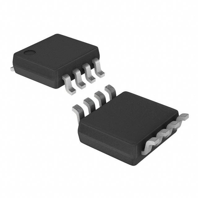
| 产品图片 |
|
| rohs | 符合RoHS无铅 / 符合限制有害物质指令(RoHS)规范要求 |
| 产品系列 | 电源管理 IC,监控电路,Texas Instruments TL7700CDGKT- |
| NumberofInputsMonitored | 1 Input |
| 数据手册 | |
| 产品型号 | TL7700CDGKT |
| 产品种类 | 监控电路 |
| 人工复位 | No Manual Reset |
| 供应商器件封装 | 8-VSSOP |
| 其它名称 | 296-32359-1 |
| 功率失效检测 | No |
| 包装 | 剪切带 (CT) |
| 单位重量 | 19 mg |
| 受监控电压数 | 1 |
| 商标 | Texas Instruments |
| 复位 | 低有效 |
| 复位超时 | 最大传输延迟为 10 µs |
| 安装类型 | 表面贴装 |
| 安装风格 | SMD/SMT |
| 封装 | Reel |
| 封装/外壳 | 8-TSSOP,8-MSOP(0.118",3.00mm 宽) |
| 封装/箱体 | VSSOP-8 |
| 工作温度 | -40°C ~ 85°C |
| 工作电源电流 | 1 mA |
| 工厂包装数量 | 250 |
| 最大工作温度 | + 85 C |
| 最小工作温度 | - 40 C |
| 标准包装 | 1 |
| 欠电压阈值 | 0.495 V |
| 电压-阈值 | 可调节/可选择 |
| 电池备用开关 | No Backup |
| 电源电压-最大 | 40 V |
| 电源电压-最小 | 1.8 V |
| 监视器 | No Watchdog |
| 类型 | 简单复位/加电复位 |
| 系列 | TL7700 |
| 芯片启用信号 | No Chip Enable |
| 被监测输入数 | 1 Input |
| 输出 | 开路漏极或开路集电极 |
| 输出类型 | Open Collectors |
| 过电压阈值 | 0.505 V |
| 重置延迟时间 | Programmable |
| 阈值电压 | 0.5 V |


- 商务部:美国ITC正式对集成电路等产品启动337调查
- 曝三星4nm工艺存在良率问题 高通将骁龙8 Gen1或转产台积电
- 太阳诱电将投资9.5亿元在常州建新厂生产MLCC 预计2023年完工
- 英特尔发布欧洲新工厂建设计划 深化IDM 2.0 战略
- 台积电先进制程称霸业界 有大客户加持明年业绩稳了
- 达到5530亿美元!SIA预计今年全球半导体销售额将创下新高
- 英特尔拟将自动驾驶子公司Mobileye上市 估值或超500亿美元
- 三星加码芯片和SET,合并消费电子和移动部门,撤换高东真等 CEO
- 三星电子宣布重大人事变动 还合并消费电子和移动部门
- 海关总署:前11个月进口集成电路产品价值2.52万亿元 增长14.8%


PDF Datasheet 数据手册内容提取
Product Sample & Technical Tools & Support & Folder Buy Documents Software Community TL7700 SLVS220G–JULY1999–REVISEDAUGUST2016 TL7700 Supply-Voltage Supervisor 1 Features 3 Description • AdjustableSenseVoltageWithTwoExternal The TL7700 is a bipolar integrated circuit designed 1 for use as a reset controller in microcomputer and Resistors microprocessor systems. The SENSE voltage can be • 1.0%SenseVoltageTolerance(25°C) set to any value greater than 0.5 V using two external • AdjustableHysteresisofSenseVoltage resistors. • WideOperatingSupply-VoltageRange: Circuit function is very stable, with supply voltage in 1.8Vto40V the 1.8-V to 40-V range. Minimum supply current • WideOperatingTemperatureRange: allows use with ac line operation, portable battery –40°Cto85°C operation, and automotive applications. The TL7700 deviceisdesignedforoperationfrom–40°Cto85°C. • LowPowerConsumption: I =0.6mATypical,V =40V CC CC DeviceInformation(1) 2 Applications PARTNUMBER PACKAGE BODYSIZE(NOM) TL7700DGK VSSOP(8) 3.00mm×3.00mm • DigitalSignalProcessors(DSPs) TL7700P PDIP(8) 9.81mm×6.35mm • Microcontrollers(MCUs) TL7700PS SO(8) 6.20mm×5.30mm • FPGAs,ASICs TL7700PW TSSOP(8) 3.00mm×4.40mm • Notebooks,DesktopComputers (1) For all available packages, see the orderable addendum at • Set-TopBoxes theendofthedatasheet. • IndustrialControlSystems FunctionalBlockDiagram VCC Vs= 500 mVTyp RESET Reference Voltage + + + SENSE − − − ICT(A) High: On R Q S IS(A) GND CT Copyright © 2016,Texas Instruments Incorporated 1 An IMPORTANT NOTICE at the end of this data sheet addresses availability, warranty, changes, use in safety-critical applications, intellectualpropertymattersandotherimportantdisclaimers.PRODUCTIONDATA.
TL7700 SLVS220G–JULY1999–REVISEDAUGUST2016 www.ti.com Table of Contents 1 Features.................................................................. 1 8.3 FeatureDescription.................................................10 2 Applications........................................................... 1 8.4 DeviceFunctionalModes........................................12 3 Description............................................................. 1 9 ApplicationandImplementation........................ 13 4 RevisionHistory..................................................... 2 9.1 ApplicationInformation............................................13 9.2 TypicalApplication .................................................13 5 PinConfigurationandFunctions......................... 3 10 PowerSupplyRecommendations..................... 15 6 Specifications......................................................... 4 11 Layout................................................................... 15 6.1 AbsoluteMaximumRatings......................................4 6.2 ESDRatings..............................................................4 11.1 LayoutGuidelines.................................................15 6.3 RecommendedOperatingConditions.......................4 11.2 LayoutExample....................................................15 6.4 ThermalInformation..................................................4 12 DeviceandDocumentationSupport................. 16 6.5 ElectricalCharacteristics...........................................5 12.1 ReceivingNotificationofDocumentationUpdates16 6.6 SwitchingCharacteristics..........................................5 12.2 CommunityResource............................................16 6.7 TypicalCharacteristics..............................................6 12.3 Trademarks...........................................................16 7 ParameterMeasurementInformation..................8 12.4 ElectrostaticDischargeCaution............................16 12.5 Glossary................................................................16 8 DetailedDescription............................................ 10 13 Mechanical,Packaging,andOrderable 8.1 Overview.................................................................10 Information........................................................... 16 8.2 FunctionalBlockDiagram.......................................10 4 Revision History NOTE:Pagenumbersforpreviousrevisionsmaydifferfrompagenumbersinthecurrentversion. ChangesfromRevisionF(August2011)toRevisionG Page • AddedESDRatingstable,FeatureDescriptionsection,DeviceFunctionalModes,ApplicationandImplementation section,PowerSupplyRecommendationssection,Layoutsection,DeviceandDocumentationSupportsection,and Mechanical,Packaging,andOrderableInformationsection ................................................................................................. 1 • DeletedOrderingInformationtable,seePOAattheendofthedatasheet........................................................................... 1 • ChangedvaluesintheThermalInformationtabletoalignwithJEDECstandards................................................................ 4 2 SubmitDocumentationFeedback Copyright©1999–2016,TexasInstrumentsIncorporated ProductFolderLinks:TL7700
TL7700 www.ti.com SLVS220G–JULY1999–REVISEDAUGUST2016 5 Pin Configuration and Functions DGKPackage 8-PinVSSOP P,PS,orPWPackage TopView 8-PinPDIP,SO,TSSOP TopView RESET 1 8 V CC CT 1 8 RESET NC 2 7 NC SENSE 2 7 NC CT 3 6 NC NC 3 6 NC SENSE 4 5 GND GND 4 5 V CC NC–No internal connection PinFunctions PIN PDIP, I/O DESCRIPTION NAME SO, VSSOP TSSOP Timingcapacitorconnection. ThisterminalsetstheRESEToutputpulseduration(t ).Itisconnectedinternallytoa po 15-µAconstant-currentsource.Thereisalimitontheswitchingspeedofinternal elements;evenifCTissetto0,responsespeedsremainatapproximately5to10µs. CT 1 3 I/O IfCTisopen,thedevicecanbeusedasanadjustable-thresholdnoninverting comparator.IfCTislow,theinternaloutput-stagecomparatorisactive,andtheRESET outputtransistorison.Anexternalvoltagemustnotbeappliedtothisterminalduetothe internalstructureofthedevice.Therefore,drivethedeviceusinganopen-collector transistor,FET,or3-statebuffer(inthelow-levelorhigh-impedancestate). Ground GND 4 5 — Keepthisterminalaslowimpedanceaspossibletoreducecircuitnoise. NC 3,6,7 2,6,7 — Nointernalconnection Resetoutput Thisterminalcanbeconnecteddirectlytoasystemthatresetsintheactive-lowstate.A RESET 8 1 O pullupresistorusuallyisrequiredbecausetheoutputisannpnopen-collectortransistor. Anadditionaltransistorshouldbeconnectedwhentheactive-highresetorhigheroutput currentisrequired. Voltagesense Thisterminalhasathresholdlevelof500mV.Thesensevoltageandhysteresiscanbe SENSE 2 4 I setatthesametimewhenthetwovoltage-dividingresistorsareconnected.The referencevoltageistemperaturecompensatedtoinhibittemperaturedriftinthethreshold voltagewithintheoperatingtemperaturerange. Powersupply V 5 8 — CC Thisterminalisusedinanoperating-voltagerangeof1.8Vto40V. Copyright©1999–2016,TexasInstrumentsIncorporated SubmitDocumentationFeedback 3 ProductFolderLinks:TL7700
TL7700 SLVS220G–JULY1999–REVISEDAUGUST2016 www.ti.com 6 Specifications 6.1 Absolute Maximum Ratings overoperatingfree-airtemperaturerange(unlessotherwisenoted)(1) MIN MAX UNIT V Supplyvoltage(2) 41 V CC V Senseinputvoltage –0.3 41 V s V Outputvoltage(offstate) 41 V OH I Outputcurrent(onstate) 5 mA OL T Operatingvirtual-junctiontemperature 150 °C J T Storagetemperature –65 150 °C stg (1) StressesbeyondthoselistedunderAbsoluteMaximumRatingsmaycausepermanentdamagetothedevice.Thesearestressratings only,whichdonotimplyfunctionaloperationofthedeviceattheseoranyotherconditionsbeyondthoseindicatedunderRecommended OperatingConditions.Exposuretoabsolute-maximum-ratedconditionsforextendedperiodsmayaffectdevicereliability. (2) Allvoltagevaluesarewithrespecttothenetworkgroundterminal. 6.2 ESD Ratings VALUE UNIT Human-bodymodel(HBM),perANSI/ESDA/JEDECJS-001(1) 500 V(ESD) Electrostaticdischarge Charged-devicemodel(CDM),perJEDECspecificationJESD22- V C101(2) 1000 (1) JEDECdocumentJEP155statesthat500-VHBMallowssafemanufacturingwithastandardESDcontrolprocess. (2) JEDECdocumentJEP157statesthat250-VCDMallowssafemanufacturingwithastandardESDcontrolprocess. 6.3 Recommended Operating Conditions MIN MAX UNIT V Supplyvoltage 1.8 40 V CC I Low-leveloutputcurrent 3 mA OL T Operatingfree-airtemperature –40 85 °C A 6.4 Thermal Information TL7700 THERMALMETRIC(1) DGK P PS PW UNIT (VSSOP) (PDIP) (SO) (TSSOP) 8PINS 8PINS 8PINS 8PINS R Junction-to-ambientthermalresistance 173.8 57.6 112.5 172.9 °C/W θJA R Junction-to-case(top)thermalresistance 63.1 47.4 64.2 56.6 °C/W θJC(top) R Junction-to-boardthermalresistance 93.9 34.7 61.6 101.2 °C/W θJB ψ Junction-to-topcharacterizationparameter 8.5 25 25.1 5.2 °C/W JT ψ Junction-to-boardcharacterizationparameter 92.5 34.6 60.7 99.6 °C/W JB (1) Formoreinformationabouttraditionalandnewthermalmetrics,seetheSemiconductorandICPackageThermalMetricsapplication report. 4 SubmitDocumentationFeedback Copyright©1999–2016,TexasInstrumentsIncorporated ProductFolderLinks:TL7700
TL7700 www.ti.com SLVS220G–JULY1999–REVISEDAUGUST2016 6.5 Electrical Characteristics V =3V(unlessotherwisenoted) CC PARAMETER TESTCONDITIONS T MIN TYP MAX UNIT A 25°C 495 500 505 V SENSEinputvoltage mV s –40°Cto85°C 490 510 25°C 2 2.5 3 I SENSEinputcurrent V =0.4V µA s s –40°Cto85°C 1.5 3.5 I Supplycurrent V =40V,V =0.6V,Noload 25°C 0.6 1 mA CC CC s I =1.5mA 25°C 0.4 OL V Low-leveloutputvoltage V OL I =3mA 25°C 0.8 OL I High-leveloutputcurrent V =40V,V =0.6V –40°Cto85°C 1 µA OH OH s I Timing-capacitorchargecurrent V =0.6V 25°C 11 15 19 µA CT s 6.6 Switching Characteristics V =3V,T =25°C(unlessotherwisenoted) CC A PARAMETER TESTCONDITIONS MIN TYP MAX UNIT t SENSEpulseduration C =0.01µF(SeeFigure17) 2 µs pi T t Outputpulseduration C =0.01µF(SeeFigure17) 0.5 1 1.5 ms po T C =0.01µF,R =2.2kΩ,C =100pF t Outputrisetime T L L 15 µs r (SeeFigure17) C =0.01µF,R =2.2kΩ,C =100pF t Outputfalltime T L L 0.5 µs f (SeeFigure17) t Propagationdelaytime,SENSEtooutput C =0.01µF(SeeFigure17) 10 µs pd T Copyright©1999–2016,TexasInstrumentsIncorporated SubmitDocumentationFeedback 5 ProductFolderLinks:TL7700
TL7700 SLVS220G–JULY1999–REVISEDAUGUST2016 www.ti.com 6.7 Typical Characteristics Dataathighandlowtemperaturesareapplicableonlywithintherecommendedoperatingconditions. 1.2 16 A TA=−40°C m mA 1.0 nt− 15 e Supply Current− 000...468 TTTAAA=== −82554°°0CC°C citor Charge Curr 111234 TTAA== 8255°°CC −CC Capa I 0.2 ng- 11 mi Ti 0 10 0 10 20 30 40 50 60 0 10 20 30 40 50 60 VCC−Supply Voltage−V VCC−Supply Voltage−V Figure1.SupplyCurrentvsSupplyVoltage Figure2.TimingCapacitorChargeCurrentvsSupply Voltage 1.2 506 TA= 25°C −V 1.0 504 Vs= 500.8 mV ge mV 502 −Low-oltaLevel Output VVOL 0000....2468 TTATAA===− 248505°°°CCC −Sense Inoltage−put VVs 444445999990024680 TVAs== 2459°8C.3 mV 0 488 0 1 2 3 4 5 6 −75−50 −25 0 25 50 75 100 125 150 IOL−Low-Level Output Current−mA TA−Free-Air Temperature−°C Figure3.V vsI Figure4.SenseInputVoltagevsTemperature OL OL 3.5 109 3.0 s 108 A m mSense Input Current− 01122.....50505 Output Pulse Duration− 111110000034567 −Is 0 −po 102 −0.5 t 101 −1.0 1 0 0.1 0.2 0.3 0.4 0.5 0.6 1.0 10 40 1 101 102 103 104 105 106 107 108 109 Vs−Sense Input Voltage−V Ct−Timing Capacitor−pF Figure5.SenseInputCurrentvsSenseInputVoltage Figure6.OutputPulseDurationvsTimingCapacitor 6 SubmitDocumentationFeedback Copyright©1999–2016,TexasInstrumentsIncorporated ProductFolderLinks:TL7700
TL7700 www.ti.com SLVS220G–JULY1999–REVISEDAUGUST2016 Typical Characteristics (continued) Dataathighandlowtemperaturesareapplicableonlywithintherecommendedoperatingconditions. Test Point 1 2.2 kΩ TP1 onon 240 kΩ VCC DivisiDivisi RESET TPeosintt 2 P1) = 1 V/P2) = 2 V/ TP2 Vs SENSE CT 5 V TT xis (xis ( 30 kΩ GND AA Y-Y- 100 pF 510 pF X-Axis = 0.2 ms/Division Figure7.VCCvsOutputWaveform1-SeeFigure8 Figure8.VCCvsOutputTestCircuit1 Test Point 1 nn TP1 2.2 kΩ oo visivisi 240 kΩ VCC = 1 V/Di= 2 V/Di Vs RESET TPeosintt 2 P1) P2) TP2 SENSE 5 V TT s (s ( CT xixi Y-AY-A 30 kΩ GND 100 pF 510 pF X-Axis = 0.2 ms/Division Figure9.VCCvsOutputWaveform2-SeeFigure10 Figure10.VCCvsOutputTestCircuit2 Test Point 1 DivisionDivision TP1 240 kW VCRCESET 2.2 kTPWeosintt 2 V/V/ Vs 1 2 SENSE P1) = P2) = TP2 CT TT xis (xis ( 30 kW GND AA Y-Y- 100 pF 510 pF X-Axis = 0.2 ms/Division Figure11.VCCvsOutputWaveform3-SeeFigure12 Figure12.VCCvsOutputTestCircuit3 Copyright©1999–2016,TexasInstrumentsIncorporated SubmitDocumentationFeedback 7 ProductFolderLinks:TL7700
TL7700 SLVS220G–JULY1999–REVISEDAUGUST2016 www.ti.com 7 Parameter Measurement Information − + A V CC V s SENSE V CC 0.6 V GND Figure13. V vsI MeasurementCircuit CC CC V CC V s SENSE CT V CC + 0.6 V GND A − Figure14. V vsI MeasurementCircuit CC CT Test Point V CC RESET Vs 3 V SENSE CT 0.4 V GND 0.01mF Figure15. I vsV MeasurementCircuit OL OL 8 SubmitDocumentationFeedback Copyright©1999–2016,TexasInstrumentsIncorporated ProductFolderLinks:TL7700
TL7700 www.ti.com SLVS220G–JULY1999–REVISEDAUGUST2016 Parameter Measurement Information (continued) 2.2 kW V CC Test RESET Point + A − Vs SENSE VCC CT V s GND 0.01mF Figure16. V ,I CharacteristicsMeasurementCircuit s s 2.2 kW VCC Test Point RESET Vs SENSE 3 V CT GND 100 pF Ct Figure17. SwitchingCharacteristicsMeasurementCircuit Copyright©1999–2016,TexasInstrumentsIncorporated SubmitDocumentationFeedback 9 ProductFolderLinks:TL7700
TL7700 SLVS220G–JULY1999–REVISEDAUGUST2016 www.ti.com 8 Detailed Description 8.1 Overview The TL7700 is a bipolar integrated circuit designed for use as a reset controller in microcomputer and microprocessor systems. The SENSE voltage can be set to any value greater than 0.5 V using two external resistors. The hysteresis value of the sense voltage also can be set by the same resistors. The device includes a precision voltage reference, fast comparator, timing generator, and output driver, so it can generate a power-on resetsignalinadigitalsystem. The TL7700 has an internal 1.5-V temperature-compensated voltage reference from which all function blocks are supplied. Circuit function is very stable, with supply voltage in the 1.8-V to 40-V range. Minimum supply current allowsusewithaclineoperation,portablebatteryoperation,andautomotiveapplications. 8.2 Functional Block Diagram VCC Vs= 500 mVTyp RESET Reference Voltage + + + SENSE − − − ICT(A) High: On R Q S IS(A) GND CT Copyright © 2016,Texas Instruments Incorporated A. I =15µA(Typ),I =2.5µA(Typ) CT s 8.3 Feature Description 8.3.1 Sense-VoltageSetting The SENSE terminal input voltage, Vs, of the TL7700 typically is 500 mV. By using two external resistors, the circuit designer can obtain any sense voltage over 500 mV. In Figure 18, the sensing voltage, Vs', is calculated as: V =V ×(R1+R2)/R2 s' s where • V =500mVtypatT =25°C (1) s A At room temperature, V has a variation of 500 mV ± 5 mV. In the basic circuit shown in Figure 18, variations of s [±5 ± (R1+R2)/R2]mVaresuperimposedonV . s 10 SubmitDocumentationFeedback Copyright©1999–2016,TexasInstrumentsIncorporated ProductFolderLinks:TL7700
TL7700 www.ti.com SLVS220G–JULY1999–REVISEDAUGUST2016 Feature Description (continued) V CC R L R1 VCC RESET RESET V s SENSE CT R2 GND C t GND Figure18. SettingtheSenseVoltage 8.3.2 Sense-VoltageHysteresisSetting If the sense voltage (V ) does not have hysteresis in it, and the voltage on the sensing line contains ripples, the s' resetting of TL7700 is unstable. Hysteresis is added to the sense voltage to prevent such problems. As shown in Figure19,thehysteresis(V )isadded,andthevalueisdeterminedas: hys V =I ×R1 hys s where • I =2.5μAtypatT =25°C (2) s A At room temperature, I has variations of 2.5 µA ± 0.5 µA. Therefore, in the circuit shown in Figure 18, V has s hys variations of (±0.5 × R1) µV. In circuit design, it is necessary to consider the voltage-dividing resistor tolerance andtemperaturecoefficientinadditiontovariationsinV andV . s hys VCC Vhys Vs’ 1.5 V T RESET tpo tpo T Thesensevoltage,V ,isdifferentfromtheSENSEterminalinputvoltage,V .V normallyis500mVfortriggering. s' s s Figure19. V -RESETTimingChart CC Copyright©1999–2016,TexasInstrumentsIncorporated SubmitDocumentationFeedback 11 ProductFolderLinks:TL7700
TL7700 SLVS220G–JULY1999–REVISEDAUGUST2016 www.ti.com Feature Description (continued) 8.3.3 OutputPulse-DurationSetting Constant-current charging starts on the timing capacitor when the sensing-line voltage reaches the TL7700 sense voltage. When the capacitor voltage exceeds the threshold level of the output drive comparator, RESET changes from a low to a high level. The output pulse duration is the time between the point when the sense-pin voltage exceeds the threshold level and the point when the RESET output changes from a low level to a high level. When the TL7700 is used for system power-on reset, the output pulse duration, t , must be set longer po thanthepowerrisetime.Thevalueoft is: po t =C ×105seconds po t where • C isthetimingcapacitorinfarads (3) t There is a limit on the device response speed. Even if C = 0, t is not 0, but approximately 5 µs to 10 µs. t po Therefore, when the TL7700 is used as a comparator with hysteresis without connecting C, switching speeds t (t/t,t /t ,andsoforth)mustbeconsidered. r f po pd 8.4 Device Functional Modes Figure 20 describes how the RESET output pin responds to a change in the voltage at the sense pin. When the sensepindropsbelow500mV,the RESETpinispulledlow. VCC Vhys Vs’ 1.5 V T RESET tpo tpo T Thesensevoltage,V ,isdifferentfromtheSENSEterminalinputvoltage,V .V normallyis500mVfortriggering. s' s s Figure20. V RESETResponseandTiming CC 12 SubmitDocumentationFeedback Copyright©1999–2016,TexasInstrumentsIncorporated ProductFolderLinks:TL7700
TL7700 www.ti.com SLVS220G–JULY1999–REVISEDAUGUST2016 9 Application and Implementation NOTE Information in the following applications sections is not part of the TI component specification, and TI does not warrant its accuracy or completeness. TI’s customers are responsible for determining suitability of components for their purposes. Customers should validateandtesttheirdesignimplementationtoconfirmsystemfunctionality. 9.1 Application Information The TL7700 supply-voltage supervisor allows for any voltage greater than 500mV to be monitored. This flexibility allowsittobeusedinmanyapplicationsfromFPGAsandMicrocontrollerstoIndustrialsupplymonitoring. 9.2 Typical Application Figure 21 shows an application where the TL7700 device is being used to sense the voltage supply for a microcontroller that is supplied with 5 V. If the sense voltage drops below 4.5 V, the RESET pin is pulled LOW, signalingthemicrocontrollertoreset. 5V 240 k(cid:159) VCC 2.2 k(cid:159) VCC SENSE RESET RESET TL7700 Microcontroller 30 k(cid:159) CT GND VSS 510 pF Copyright © 2016, Texas Instruments Incorporated Figure21. 5-VSupplyVoltageSupervision 9.2.1 DesignRequirements • When the TL7700 is used for system power-on reset, the output pulse duration, t , must be set longer than po thepowerrisetime.Thevalueoft is:t =C ×105seconds po po t • TheRESEToutputisanopen-collectoroutput,soapullupresistorisrequired. 9.2.2 DetailedDesignProcedure The SENSE terminal input voltage, Vs, of the TL7700 typically is 500 mV. By using two external resistors, any sensevoltageover500mVcanbesensed. Resistor R1 should be selected first to set the desired hysteresis. See Sense-Voltage Hysteresis Setting for detailedinformationonhowtosetthehysteresis. Resistor R2 should then be selected based on the R1 value and the desired V voltage. In Figure 18, the s' sensingvoltage,V ,iscalculatedas:V =V ×(R1+R2)/R2 s' s' s Copyright©1999–2016,TexasInstrumentsIncorporated SubmitDocumentationFeedback 13 ProductFolderLinks:TL7700
TL7700 SLVS220G–JULY1999–REVISEDAUGUST2016 www.ti.com Typical Application (continued) 9.2.3 ApplicationCurve 506 TA= 25°C 504 Vs= 500.8 mV V m 502 − ge 500 a oltV 498 ut p 496 n se I 494 TA= 25°C n Se Vs= 498.3 mV − 492 s V 490 488 −75 −50 −25 0 25 50 75 100 125 150 TA−Free-Air Temperature−°C Figure22.SenseInputVoltagevsTemperature 14 SubmitDocumentationFeedback Copyright©1999–2016,TexasInstrumentsIncorporated ProductFolderLinks:TL7700
TL7700 www.ti.com SLVS220G–JULY1999–REVISEDAUGUST2016 10 Power Supply Recommendations The TL7700 device will operate within the supply range specified in Recommended Operating Conditions. The deviceriskspermanentdamageoverthevoltagespecifiedinAbsoluteMaximumRatings. 11 Layout 11.1 Layout Guidelines Figure 23 shows an example layout for the TL7700 device. As the RESET pin is an open collector output, a pullupresistorisrequiredtoensuretheoutputishighwhentheoutputtransistorisoff. 11.2 Layout Example 2.2 k(cid:13) 5V 1 RESET VCC 8 2 NC NC 7 240 k(cid:13) 3 CT NC 6 30 k(cid:13) 510 pF 4 SENSE GND 5 GND Figure23. DGKPackageExampleLayoutfor5VSupplySupervision Copyright©1999–2016,TexasInstrumentsIncorporated SubmitDocumentationFeedback 15 ProductFolderLinks:TL7700
TL7700 SLVS220G–JULY1999–REVISEDAUGUST2016 www.ti.com 12 Device and Documentation Support 12.1 Receiving Notification of Documentation Updates To receive notification of documentation updates, navigate to the device product folder on ti.com. In the upper right corner, click on Alert me to register and receive a weekly digest of any product information that has changed.Forchangedetails,reviewtherevisionhistoryincludedinanyreviseddocument. 12.2 Community Resource The following links connect to TI community resources. Linked contents are provided "AS IS" by the respective contributors. They do not constitute TI specifications and do not necessarily reflect TI's views; see TI's Terms of Use. TIE2E™OnlineCommunity TI'sEngineer-to-Engineer(E2E)Community.Createdtofostercollaboration amongengineers.Ate2e.ti.com,youcanaskquestions,shareknowledge,exploreideasandhelp solveproblemswithfellowengineers. DesignSupport TI'sDesignSupport QuicklyfindhelpfulE2Eforumsalongwithdesignsupporttoolsand contactinformationfortechnicalsupport. 12.3 Trademarks E2EisatrademarkofTexasInstruments. Allothertrademarksarethepropertyoftheirrespectiveowners. 12.4 Electrostatic Discharge Caution This integrated circuit can be damaged by ESD. Texas Instruments recommends that all integrated circuits be handled with appropriateprecautions.Failuretoobserveproperhandlingandinstallationprocedurescancausedamage. ESDdamagecanrangefromsubtleperformancedegradationtocompletedevicefailure.Precisionintegratedcircuitsmaybemore susceptibletodamagebecauseverysmallparametricchangescouldcausethedevicenottomeetitspublishedspecifications. 12.5 Glossary SLYZ022—TIGlossary. Thisglossarylistsandexplainsterms,acronyms,anddefinitions. 13 Mechanical, Packaging, and Orderable Information The following pages include mechanical, packaging, and orderable information. This information is the most current data available for the designated devices. This data is subject to change without notice and revision of thisdocument.Forbrowser-basedversionsofthisdatasheet,refertotheleft-handnavigation. 16 SubmitDocumentationFeedback Copyright©1999–2016,TexasInstrumentsIncorporated ProductFolderLinks:TL7700
PACKAGE OPTION ADDENDUM www.ti.com 6-Feb-2020 PACKAGING INFORMATION Orderable Device Status Package Type Package Pins Package Eco Plan Lead/Ball Finish MSL Peak Temp Op Temp (°C) Device Marking Samples (1) Drawing Qty (2) (6) (3) (4/5) TL7700CDGKR ACTIVE VSSOP DGK 8 2500 Green (RoHS NIPDAU Level-1-260C-UNLIM -40 to 85 9TS & no Sb/Br) TL7700CDGKT ACTIVE VSSOP DGK 8 250 Green (RoHS NIPDAU Level-1-260C-UNLIM -40 to 85 9TS & no Sb/Br) TL7700CP ACTIVE PDIP P 8 50 Green (RoHS NIPDAU N / A for Pkg Type -40 to 85 TL7700CP & no Sb/Br) TL7700CPS ACTIVE SO PS 8 80 Green (RoHS NIPDAU Level-1-260C-UNLIM T7700 & no Sb/Br) TL7700CPSR ACTIVE SO PS 8 2000 Green (RoHS NIPDAU Level-1-260C-UNLIM -40 to 85 T7700 & no Sb/Br) TL7700CPW ACTIVE TSSOP PW 8 150 Green (RoHS NIPDAU Level-1-260C-UNLIM -40 to 85 T7700 & no Sb/Br) TL7700CPWG4 ACTIVE TSSOP PW 8 150 Green (RoHS NIPDAU Level-1-260C-UNLIM -40 to 85 T7700 & no Sb/Br) TL7700CPWR ACTIVE TSSOP PW 8 2000 Green (RoHS NIPDAU Level-1-260C-UNLIM -40 to 85 T7700 & no Sb/Br) TL7700CPWRE4 ACTIVE TSSOP PW 8 2000 Green (RoHS NIPDAU Level-1-260C-UNLIM -40 to 85 T7700 & no Sb/Br) TL7700CPWRG4 ACTIVE TSSOP PW 8 2000 Green (RoHS NIPDAU Level-1-260C-UNLIM -40 to 85 T7700 & no Sb/Br) (1) The marketing status values are defined as follows: ACTIVE: Product device recommended for new designs. LIFEBUY: TI has announced that the device will be discontinued, and a lifetime-buy period is in effect. NRND: Not recommended for new designs. Device is in production to support existing customers, but TI does not recommend using this part in a new design. PREVIEW: Device has been announced but is not in production. Samples may or may not be available. OBSOLETE: TI has discontinued the production of the device. (2) RoHS: TI defines "RoHS" to mean semiconductor products that are compliant with the current EU RoHS requirements for all 10 RoHS substances, including the requirement that RoHS substance do not exceed 0.1% by weight in homogeneous materials. Where designed to be soldered at high temperatures, "RoHS" products are suitable for use in specified lead-free processes. TI may reference these types of products as "Pb-Free". RoHS Exempt: TI defines "RoHS Exempt" to mean products that contain lead but are compliant with EU RoHS pursuant to a specific EU RoHS exemption. Green: TI defines "Green" to mean the content of Chlorine (Cl) and Bromine (Br) based flame retardants meet JS709B low halogen requirements of <=1000ppm threshold. Antimony trioxide based flame retardants must also meet the <=1000ppm threshold requirement. (3) MSL, Peak Temp. - The Moisture Sensitivity Level rating according to the JEDEC industry standard classifications, and peak solder temperature. Addendum-Page 1
PACKAGE OPTION ADDENDUM www.ti.com 6-Feb-2020 (4) There may be additional marking, which relates to the logo, the lot trace code information, or the environmental category on the device. (5) Multiple Device Markings will be inside parentheses. Only one Device Marking contained in parentheses and separated by a "~" will appear on a device. If a line is indented then it is a continuation of the previous line and the two combined represent the entire Device Marking for that device. (6) Lead/Ball Finish - Orderable Devices may have multiple material finish options. Finish options are separated by a vertical ruled line. Lead/Ball Finish values may wrap to two lines if the finish value exceeds the maximum column width. Important Information and Disclaimer:The information provided on this page represents TI's knowledge and belief as of the date that it is provided. TI bases its knowledge and belief on information provided by third parties, and makes no representation or warranty as to the accuracy of such information. Efforts are underway to better integrate information from third parties. TI has taken and continues to take reasonable steps to provide representative and accurate information but may not have conducted destructive testing or chemical analysis on incoming materials and chemicals. TI and TI suppliers consider certain information to be proprietary, and thus CAS numbers and other limited information may not be available for release. In no event shall TI's liability arising out of such information exceed the total purchase price of the TI part(s) at issue in this document sold by TI to Customer on an annual basis. Addendum-Page 2
PACKAGE MATERIALS INFORMATION www.ti.com 20-Dec-2018 TAPE AND REEL INFORMATION *Alldimensionsarenominal Device Package Package Pins SPQ Reel Reel A0 B0 K0 P1 W Pin1 Type Drawing Diameter Width (mm) (mm) (mm) (mm) (mm) Quadrant (mm) W1(mm) TL7700CDGKR VSSOP DGK 8 2500 330.0 12.4 5.3 3.4 1.4 8.0 12.0 Q1 TL7700CDGKT VSSOP DGK 8 250 177.8 12.4 5.3 3.4 1.4 8.0 12.0 Q1 TL7700CPWR TSSOP PW 8 2000 330.0 12.4 7.0 3.6 1.6 8.0 12.0 Q1 TL7700CPWRG4 TSSOP PW 8 2000 330.0 12.4 7.0 3.6 1.6 8.0 12.0 Q1 PackMaterials-Page1
PACKAGE MATERIALS INFORMATION www.ti.com 20-Dec-2018 *Alldimensionsarenominal Device PackageType PackageDrawing Pins SPQ Length(mm) Width(mm) Height(mm) TL7700CDGKR VSSOP DGK 8 2500 358.0 335.0 35.0 TL7700CDGKT VSSOP DGK 8 250 358.0 335.0 35.0 TL7700CPWR TSSOP PW 8 2000 367.0 367.0 35.0 TL7700CPWRG4 TSSOP PW 8 2000 367.0 367.0 35.0 PackMaterials-Page2
None
None
None
None
None
PACKAGE OUTLINE PW0008A TSSOP - 1.2 mm max height SCALE 2.800 SMALL OUTLINE PACKAGE C 6.6 TYP SEATING PLANE 6.2 PIN 1 ID A 0.1 C AREA 6X 0.65 8 1 3.1 2X 2.9 NOTE 3 1.95 4 5 0.30 8X 0.19 4.5 1.2 MAX B 0.1 C A B 4.3 NOTE 4 (0.15) TYP SEE DETAIL A 0.25 GAGE PLANE 0.15 0.75 0 - 8 0.05 0.50 DETAIL A TYPICAL 4221848/A 02/2015 NOTES: 1. All linear dimensions are in millimeters. Any dimensions in parenthesis are for reference only. Dimensioning and tolerancing per ASME Y14.5M. 2. This drawing is subject to change without notice. 3. This dimension does not include mold flash, protrusions, or gate burrs. Mold flash, protrusions, or gate burrs shall not exceed 0.15 mm per side. 4. This dimension does not include interlead flash. Interlead flash shall not exceed 0.25 mm per side. 5. Reference JEDEC registration MO-153, variation AA. www.ti.com
EXAMPLE BOARD LAYOUT PW0008A TSSOP - 1.2 mm max height SMALL OUTLINE PACKAGE 8X (1.5) 8X (0.45) SYMM (R0.05) 1 TYP 8 SYMM 6X (0.65) 5 4 (5.8) LAND PATTERN EXAMPLE SCALE:10X SOOPLEDNEINRG MASK METAL MSOELTDAEL RU NMDAESRK SOOPLEDNEINRG MASK 0.05 MAX 0.05 MIN ALL AROUND ALL AROUND NON SOLDER MASK SOLDER MASK DEFINED DEFINED SOLDER MASK DETAILS NOT TO SCALE 4221848/A 02/2015 NOTES: (continued) 6. Publication IPC-7351 may have alternate designs. 7. Solder mask tolerances between and around signal pads can vary based on board fabrication site. www.ti.com
EXAMPLE STENCIL DESIGN PW0008A TSSOP - 1.2 mm max height SMALL OUTLINE PACKAGE 8X (1.5) SYMM (R0.05) TYP 8X (0.45) 1 8 SYMM 6X (0.65) 5 4 (5.8) SOLDER PASTE EXAMPLE BASED ON 0.125 mm THICK STENCIL SCALE:10X 4221848/A 02/2015 NOTES: (continued) 8. Laser cutting apertures with trapezoidal walls and rounded corners may offer better paste release. IPC-7525 may have alternate design recommendations. 9. Board assembly site may have different recommendations for stencil design. www.ti.com
IMPORTANTNOTICEANDDISCLAIMER TI PROVIDES TECHNICAL AND RELIABILITY DATA (INCLUDING DATASHEETS), DESIGN RESOURCES (INCLUDING REFERENCE DESIGNS), APPLICATION OR OTHER DESIGN ADVICE, WEB TOOLS, SAFETY INFORMATION, AND OTHER RESOURCES “AS IS” AND WITH ALL FAULTS, AND DISCLAIMS ALL WARRANTIES, EXPRESS AND IMPLIED, INCLUDING WITHOUT LIMITATION ANY IMPLIED WARRANTIES OF MERCHANTABILITY, FITNESS FOR A PARTICULAR PURPOSE OR NON-INFRINGEMENT OF THIRD PARTY INTELLECTUAL PROPERTY RIGHTS. These resources are intended for skilled developers designing with TI products. You are solely responsible for (1) selecting the appropriate TI products for your application, (2) designing, validating and testing your application, and (3) ensuring your application meets applicable standards, and any other safety, security, or other requirements. These resources are subject to change without notice. TI grants you permission to use these resources only for development of an application that uses the TI products described in the resource. Other reproduction and display of these resources is prohibited. No license is granted to any other TI intellectual property right or to any third party intellectual property right. TI disclaims responsibility for, and you will fully indemnify TI and its representatives against, any claims, damages, costs, losses, and liabilities arising out of your use of these resources. TI’s products are provided subject to TI’s Terms of Sale (www.ti.com/legal/termsofsale.html) or other applicable terms available either on ti.com or provided in conjunction with such TI products. TI’s provision of these resources does not expand or otherwise alter TI’s applicable warranties or warranty disclaimers for TI products. Mailing Address: Texas Instruments, Post Office Box 655303, Dallas, Texas 75265 Copyright © 2020, Texas Instruments Incorporated