ICGOO在线商城 > 集成电路(IC) > PMIC - 监控器 > TL7757IPK
 Datasheet下载
- 型号: TL7757IPK
- 制造商: Texas Instruments
- 库位|库存: xxxx|xxxx
- 要求:
| 数量阶梯 | 香港交货 | 国内含税 |
| +xxxx | $xxxx | ¥xxxx |
查看当月历史价格
查看今年历史价格
TL7757IPK产品简介:
ICGOO电子元器件商城为您提供TL7757IPK由Texas Instruments设计生产,在icgoo商城现货销售,并且可以通过原厂、代理商等渠道进行代购。 TL7757IPK价格参考¥1.72-¥4.94。Texas InstrumentsTL7757IPK封装/规格:PMIC - 监控器, 开路漏极或开路集电极 监控器 1 通道 SOT-89-3。您可以下载TL7757IPK参考资料、Datasheet数据手册功能说明书,资料中有TL7757IPK 详细功能的应用电路图电压和使用方法及教程。
Texas Instruments(德州仪器)的TL7757IPK是一款PMIC(电源管理集成电路)中的电压监控器,主要用于监测系统电压以确保其处于安全和稳定的工作范围内。以下是该型号的应用场景:

 1. 嵌入式系统
   - TL7757IPK广泛应用于嵌入式控制系统中,例如工业自动化设备、家用电器控制器等。它能够实时监控系统主电源电压,当电压低于预设阈值时,触发复位信号以保护系统免受低电压影响。

 2. 微控制器保护
   - 在基于微控制器的系统中,TL7757IPK可以防止因电源波动导致的微控制器异常运行。通过提供精确的复位功能,确保微控制器在上电或掉电过程中可靠启动和关闭。

 3. 电池供电设备
   - 对于依赖电池供电的便携式设备(如手持测量仪器、无线传感器节点等),TL7757IPK可以帮助检测电池电压是否过低,并及时通知用户更换或充电,从而避免数据丢失或设备损坏。

 4. 通信与网络设备
   - 在路由器、交换机或其他网络设备中,TL7757IPK可用于监控关键电路的供电状态,确保通信链路的稳定性。如果发生电压异常,它可以快速响应并采取保护措施。

 5. 汽车电子
   - 在汽车电子系统中,例如信息娱乐系统、仪表盘模块或辅助驾驶系统中,TL7757IPK可以监测车载电源电压,防止因电压波动引起的系统故障。

 6. 消费电子产品
   - 包括数字电视、机顶盒、打印机等在内的消费电子产品中,TL7757IPK能够保障设备在各种工作条件下的电压稳定性,提升用户体验。

 核心功能:
- 可调复位阈值:支持外部电阻配置复位电压阈值,适应不同应用场景。
- 快速响应时间:在电压跌落时迅速触发复位信号,保护系统硬件。
- 低功耗设计:适合对能效要求较高的应用场合。

总之,TL7757IPK适用于需要高可靠性电压监控的各种电子设备,尤其是在对电源稳定性有严格要求的工业、汽车和消费领域中表现突出。
| 参数 | 数值 |
| 产品目录 | 集成电路 (IC)半导体 |
| 描述 | IC 4.55V SUPPLY MONITOR SOT-89监控电路 4.55V Monitr/Detectr |
| 产品分类 | |
| 品牌 | Texas Instruments |
| 产品手册 | |
| 产品图片 |
|
| rohs | 符合RoHS无铅 / 符合限制有害物质指令(RoHS)规范要求 |
| 产品系列 | 电源管理 IC,监控电路,Texas Instruments TL7757IPK- |
| NumberofInputsMonitored | 1 Input |
| 数据手册 | |
| 产品型号 | TL7757IPK |
| 产品目录页面 | |
| 产品种类 | 监控电路 |
| 人工复位 | No Manual Reset |
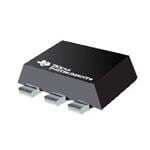
| 供应商器件封装 | SOT-89-3 |
| 其它名称 | 296-3262-1 |
| 包装 | 剪切带 (CT) |
| 受监控电压数 | 1 |
| 商标 | Texas Instruments |
| 复位 | 低有效 |
| 复位超时 | 最大传输延迟为 5 µs |
| 安装类型 | 表面贴装 |
| 安装风格 | SMD/SMT |
| 封装 | Reel |
| 封装/外壳 | TO-243AA |
| 封装/箱体 | SOT-89-3 |
| 工作温度 | -40°C ~ 85°C |
| 工作电源电流 | 1400 uA |
| 工厂包装数量 | 1000 |
| 最大工作温度 | + 85 C |
| 最小工作温度 | - 40 C |
| 标准包装 | 1 |
| 欠电压阈值 | 4.55 V |
| 电压-阈值 | 4.55V |
| 电池备用开关 | No Backup |
| 电源电压-最大 | 7 V |
| 电源电压-最小 | 1 V |
| 监视器 | No Watchdog |
| 类型 | 简单复位/加电复位 |
| 系列 | TL7757 |
| 被监测输入数 | 1 Input |
| 输出 | 开路漏极或开路集电极 |
| 输出类型 | Open Collector / Drain |
| 过电压阈值 | 4.67 V |
| 阈值电压 | 4.55 V |


- 商务部:美国ITC正式对集成电路等产品启动337调查
- 曝三星4nm工艺存在良率问题 高通将骁龙8 Gen1或转产台积电
- 太阳诱电将投资9.5亿元在常州建新厂生产MLCC 预计2023年完工
- 英特尔发布欧洲新工厂建设计划 深化IDM 2.0 战略
- 台积电先进制程称霸业界 有大客户加持明年业绩稳了
- 达到5530亿美元!SIA预计今年全球半导体销售额将创下新高
- 英特尔拟将自动驾驶子公司Mobileye上市 估值或超500亿美元
- 三星加码芯片和SET,合并消费电子和移动部门,撤换高东真等 CEO
- 三星电子宣布重大人事变动 还合并消费电子和移动部门
- 海关总署:前11个月进口集成电路产品价值2.52万亿元 增长14.8%


PDF Datasheet 数据手册内容提取
TL7757 SUPPLY-VOLTAGE SUPERVISOR AND PRECISION VOLTAGE DETECTOR SLVS041I − SEPTEMBER 1991 − REVISED AUGUST 2003 (cid:1) Power-On Reset Generator D PACKAGE (cid:1) (TOP VIEW) Automatic Reset Generation After Voltage Drop RESET 1 8 NC (cid:1) Low Standby Current...20 µA VCC 2 7 NC (cid:1) RESET Output Defined When V NC 3 6 NC CC Exceeds 1 V GND 4 5 NC (cid:1) Precision Threshold Voltage 4.55 V ±120mV NC−No internal connection (cid:1) High Output Sink Capability...20 mA (cid:1) LP PACKAGE Comparator Hysteresis Prevents Erratic (TOP VIEW) Resets description/ordering information GND V CC The TL7757 is a supply-voltage supervisor designed for use in microcomputer and RESET microprocessor systems. The supervisor monitors the supply voltage for undervoltage PK PACKAGE conditions. During power up, when the supply (TOP VIEW) voltage, V , attains a value approaching 1 V, the CC RESET RESET output becomes active (low) to prevent undefined operation. If the supply voltage drops below threshold voltage level (VIT−), the RESET GND output goes to the active (low) level until the supply undervoltage fault condition is eliminated. VCC GND is in electrical contact with the tab. ORDERING INFORMATION ORDERABLE TOP-SIDE TA PACKAGE† PART NUMBER MARKING Tube of 75 TL7757CD SSOOIICC ((DD)) 77775577CC Reel of 2500 TL7757CDR 00°CC ttoo 7700°CC SOT (PK) Reel of 1000 TL7757CPK T7 Bulk of 1000 TL7757CLP TTOO222266 // TTOO-9922 ((LLPP)) TTLL77775577CC Reel of 2000 TL7757CLPR Tube of 75 TL7757ID SSOOIICC ((DD)) 77775577II Reel of 2500 TL7757IDR −4400°CC ttoo 8855°CC SOT (PK) Reel of 1000 TL7757IPK 7I Bulk of 1000 TL7757ILP TTOO222266 // TTOO-9922 ((LLPP)) TTLL77775577II Reel of 2000 TL7757ILPR †Package drawings, standard packing quantities, thermal data, symbolization, and PCB design guidelines are available at www.ti.com/sc/package. Please be aware that an important notice concerning availability, standard warranty, and use in critical applications of TexasInstruments semiconductor products and disclaimers thereto appears at the end of this data sheet. PRODUCTION DATA information is current as of publication date. Copyright 2003, Texas Instruments Incorporated Products conform to specifications per the terms of Texas Instruments standard warranty. Production processing does not necessarily include testing of all parameters. POST OFFICE BOX 655303 • DALLAS, TEXAS 75265 1
TL7757 SUPPLY-VOLTAGE SUPERVISOR AND PRECISION VOLTAGE DETECTOR SLVS041I − SEPTEMBER 1991 − REVISED AUGUST 2003 equivalent schematic VCC RESET R2 R15 Q8 Q2 Q11 Q5 R12 R3 Q13Q15 Q19 R5 Q17 Q21 R11 C2 R16 R1 R4 Q7 Q9 Q20 R6 R10 R14 Q6 Q18 R8 Q3 Q4 Q14 C1 Q10 Q12 Q16 R18 R9 Q1 R7 R13 GND ACTUAL DEVICE COMPONENT COUNT Transistors 27 Resistors 20 Capacitors 2 absolute maximum ratings over operating junction temperature range (unless otherwise noted)† Supply voltage range, V (see Note 1) . . . . . . . . . . . . . . . . . . . . . . . . . . . . . . . . . . . . . . . . . . . . . −0.3 V to 20 V CC Off-state output voltage range (see Note 1) . . . . . . . . . . . . . . . . . . . . . . . . . . . . . . . . . . . . . . . . . . . −0.3 V to 20 V Output current, I . . . . . . . . . . . . . . . . . . . . . . . . . . . . . . . . . . . . . . . . . . . . . . . . . . . . . . . . . . . . . . . . . . . . . . . . 30 mA O Package thermal impedance, θ (see Notes 2 and 3): D package . . . . . . . . . . . . . . . . . . . . . . . . . . . . 97°C/W JA LP package . . . . . . . . . . . . . . . . . . . . . . . . . . 140°C/W PK package . . . . . . . . . . . . . . . . . . . . . . . . . . . 52°C/W Operating virtual junction temperature, T . . . . . . . . . . . . . . . . . . . . . . . . . . . . . . . . . . . . . . . . . . . . . . . . . . . 150°C J Lead temperature 1,6 mm (1/16 inch) from case for 10 seconds . . . . . . . . . . . . . . . . . . . . . . . . . . . . . . . 260°C Storage temperature range, T . . . . . . . . . . . . . . . . . . . . . . . . . . . . . . . . . . . . . . . . . . . . . . . . . . . −65°C to 150°C stg †Stresses beyond those listed under “absolute maximum ratings” may cause permanent damage to the device. These are stress ratings only, and functional operation of the device at these or any other conditions beyond those indicated under “recommended operating conditions” is not implied. Exposure to absolute-maximum-rated conditions for extended periods may affect device reliability. NOTES: 1. All voltage values are with respect to network terminal ground. 2. Maximum power dissipation is a function of TJ(max), θJA, and TA. The maximum allowable power dissipation at any allowable ambient temperature is PD = (TJ(max) − TA)/θJA. Operating at the absolute maximum TJ of 150°C can affect reliability. 3. The package thermal impedance is calculated in accordance with JESD 51-7. 2 POST OFFICE BOX 655303 • DALLAS, TEXAS 75265
TL7757 SUPPLY-VOLTAGE SUPERVISOR AND PRECISION VOLTAGE DETECTOR SLVS041I − SEPTEMBER 1991 − REVISED AUGUST 2003 recommended operating conditions MIN MAX UNIT VCC Supply voltage 1 7 V VOH High-level output voltage 15 V IOL Low-level output current 20 mA TL7757C 0 70 TTA OOppeerraattiinngg ffrreeee-aaiirr tteemmppeerraattuurree °°CC TL7757I −40 85 electrical characteristics at specified free-air temperature TL7757C PPAARRAAMMEETTEERR TTEESSTT CCOONNDDIITTIIOONNSS TTA UUNNIITT MIN TYP MAX 25°C 4.43 4.55 4.67 VVIT− NNeeggaattiivvee-ggooiinngg iinnppuutt tthhrreesshhoolldd vvoollttaaggee aatt VVCC 0°C to 70°C 4.4 4.7 VV 25°C 40 50 60 VVhys†† HHyysstteerreessiiss aatt VVCC 0°C to 70°C 30 70 mmVV 25°C 0.4 0.8 VVOL LLooww-lleevveell oouuttppuutt vvoollttaaggee IIOL = 2200 mmAA, VVCC = 44.33 VV 0°C to 70°C 0.8 VV IIOH HHiigghh-lleevveell oouuttppuutt ccuurrrreenntt VVSeCCeCC F==i g77u VVre,, 1 VVOOHH == 1155 VV,, 0°C2 t5o° C70°C 11 µAA VVres‡‡ PPoowweerr-uupp rreesseett vvoollttaaggee RRVCLL C== s22le..22w kk rΩΩa,,te ≤ 5 V/µs 0°C2 t5o° C70°C 0.8 1.12 VV 25°C 1400 2000 ICCCC Supppplyy current VVCC = 44.33 VV 0°C to 70°C 2000 µµA VCC = 5.5 V 0°C to 70°C 40 †This is the difference between positive-going input threshold voltage, VIT+, and negative-going input threshold voltage, VIT−. ‡This is the lowest voltage at which RESET becomes active. switching characteristics at specified free-air temperature TL7757C PPAARRAAMMEETTEERR TTEESSTT CCOONNDDIITTIIOONNSS TTA UUNNIITT MIN TYP MAX ttPLH PPourrootpppuaatggaattiioonn ddeellaayy ttiimmee,, llooww-ttoo-hhiigghh-lleevveell VVSeCCeCC Fssllieegwwur erraastt ee2 ≤≤a n55d VV 3//µµss,, 0°C2 t5o° C70°C 3.4 55 µss PPrrooppaaggaattiioonn ddeellaayy ttiimmee,, hhiigghh-ttoo-llooww-lleevveell 25°C 2 5 ttPHL output SSeeee FFiigguurreess 22 aanndd 33 0°C to 70°C 5 µss ttr RRiissee ttiimmee VVSeCCeCC Fssllieegwwur erraastt ee2 ≤≤a n55d VV 3//µµss,, 0°C2 t5o° C70°C 0.4 11 µss 25°C 0.05 1 ttf FFaallll ttiimmee SSeeee FFiigguurreess 22 aanndd 33 0°C to 70°C 1 µss ttw(min) MMreiisnnpiimmonuusmme ppuullssee dduurraattiioonn aatt VVCCCC ffoorr oouuttppuutt 0°C2 t5o° C70°C 55 µµss POST OFFICE BOX 655303 • DALLAS, TEXAS 75265 3
TL7757 SUPPLY-VOLTAGE SUPERVISOR AND PRECISION VOLTAGE DETECTOR SLVS041I − SEPTEMBER 1991 − REVISED AUGUST 2003 electrical characteristics at specified free-air temperature TL7757I PPAARRAAMMEETTEERR TTEESSTT CCOONNDDIITTIIOONNSS TTA UUNNIITT MIN TYP MAX 25°C 4.43 4.55 4.67 VVIT− NNeeggaattiivvee-ggooiinngg iinnppuutt tthhrreesshhoolldd vvoollttaaggee aatt VVCC −40°C to 85°C 4.4 4.7 VV 25°C 40 50 60 VVhys†† HHyysstteerreessiiss aatt VVCC −40°C to 85°C 30 70 mmVV 25°C 0.4 0.8 VVOL LLooww-lleevveell oouuttppuutt vvoollttaaggee IIOL = 2200 mmAA, VVCC = 44.33 VV −40°C to 85°C 0.8 VV IIOH HHiigghh-lleevveell oouuttppuutt ccuurrrreenntt VVSeCCeCC F==i g77u VVre,, 1 VVOOHH == 1155 VV,, −40°C25 t°oC 85°C 11 µAA VVres‡‡ PPoowweerr-uupp rreesseett vvoollttaaggee RRVCLL C== s22le..22w kk rΩΩa,,te ≤ 5 V/µs −40°C25 t°oC 85°C 0.8 1.12 VV 25°C 1400 2000 ICCCC Supppplyy current VVCC = 44.33 VV −40°C to 85°C 2100 µµA VCC = 5.5 V −40°C to 85°C 40 †This is the difference between positive-going input threshold voltage, VIT+, and negative-going input threshold voltage, VIT−. ‡This is the lowest voltage at which RESET becomes active. switching characteristics at specified free-air temperature TL7757I PPAARRAAMMEETTEERR TTEESSTT CCOONNDDIITTIIOONNSS TTA UUNNIITT MIN TYP MAX ttPLH PPrrooppaaggaattiioonn ddeellaayy ttiimmee, llooww-ttoo-hhiigghh-lleevveell oouuttppuutt VVSeCCeCC Fssllieegwwur erraastt ee2 ≤≤a n55d VV 3//µµss,, −40°C25 t°oC 85°C 3.4 55 µss 25°C 2 5 ttPHL PPrrooppaaggaattiioonn ddeellaayy ttiimmee, hhiigghh-ttoo-llooww-lleevveell oouuttppuutt SSeeee FFiigguurreess 22 aanndd 33 −40°C to 85°C 5 µss ttr RRiissee ttiimmee VVSeCCeCC Fssllieegwwur erraastt ee2 ≤≤a n55d VV 3//µµss,, −40°C25 t°oC 85°C 0.4 11 µss 25°C 0.05 1 ttf FFaallll ttiimmee SSeeee FFiigguurreess 22 aanndd 33 −40°C to 85°C 1 µss ttw(min) MMreiisnnpiimmonuusmme ppuullssee dduurraattiioonn aatt VVCCCC ffoorr oouuttppuutt −40°C25 t°oC 85°C 55 µµss 4 POST OFFICE BOX 655303 • DALLAS, TEXAS 75265
TL7757 SUPPLY-VOLTAGE SUPERVISOR AND PRECISION VOLTAGE DETECTOR SLVS041I − SEPTEMBER 1991 − REVISED AUGUST 2003 PARAMETER MEASUREMENT INFORMATION 15 V VCC A + TL7757 5.5 V RESET − GND Figure 1. Test Circuit for Output Leakage Current VCC TL7757 RL = 1 kΩ Pulse Generator 0.1 (cid:1)F RESET OUT GND CL = 100 pF (see Note A) NOTE A: Includes jig and probe capacitance Figure 2. Test Circuit for RESET Output Switching Characteristics 4.8 V (see NoteV CAC) VIT+ VIT− 4.3 V tPLH tPHL 90% 90% RESET 50% 50% 10% 10% tr tf NOTE A: VCC slew rate ≤ 5 µs Figure 3. Switching Diagram POST OFFICE BOX 655303 • DALLAS, TEXAS 75265 5
TL7757 SUPPLY-VOLTAGE SUPERVISOR AND PRECISION VOLTAGE DETECTOR SLVS041I − SEPTEMBER 1991 − REVISED AUGUST 2003 TYPICAL CHARACTERISTICS† Table of Graphs FIGURE VCC Supply voltage vs RESET output voltage 4 ICC Supply current vs Supply voltage 5 ICC Supply current vs Free-air temperature 6 Low-level output voltage vs Low-level output VOL current 7 VOL Low-level output voltage vs Free-air temperature 8 IOL Output current vs Supply voltage 9 VIT− Itnepmupt ethraretusrheold voltage (negative-going VCC) vs Free-air 10 Vres Power-up reset voltage vs Free-air temperature 11 Vres Power-up reset voltage and supply voltage vs Time 12 Propagation delay time 13 SUPPLY VOLTAGE SUPPLY CURRENT vs vs RESET OUTPUT VOLTAGE SUPPLY VOLTAGE 8 2 TA = 25°C TA = 25°C 7 IO = 0 IO = 0 V 6 A 1.5 − m e − ag 5 nt Volt urre put 4 y C 1 Out uppl T 3 S E − RES 2 Output DD CC 0.5 II Undefined 1 0 0 0 1 2 3 4 5 6 7 0 1 2 3 4 5 6 7 VCC − Supply Voltage − V VCC − Supply Voltage − V Figure 4 Figure 5 †Data at high and low temperatures are applicable only within the rated operating free-air temperature ranges of the various devices. 6 POST OFFICE BOX 655303 • DALLAS, TEXAS 75265
TL7757 SUPPLY-VOLTAGE SUPERVISOR AND PRECISION VOLTAGE DETECTOR SLVS041I − SEPTEMBER 1991 − REVISED AUGUST 2003 TYPICAL CHARACTERISTICS† SUPPLY CURRENT LOW-LEVEL OUTPUT VOLTAGE vs vs FREE-AIR TEMPERATURE LOW-LEVEL OUTPUT CURRENT 1.52 120 1.48 RL = 0 110 TA = 25°C 1.44 VCC = 4.3 V V 100 m 1.4 nt − mA 11..3326 oltage − 9800 VCC = 1 V urre 1.28 ut V 70 C p ply 0.040 Out 60 VCC = 4.3 V up el 50 D − SC 0.036 VCC = 7 V w-Lev 40 DC 0.032 o 30 II L − 0.028 VCC = 5.5 V L L 20 OO 0.024 VV 10 0.020 0 −75 − 50 − 25 0 25 50 75 100 125 0 4 8 12 16 20 TA − Free-Air Temperature − °C IOL − Low-Level Output Current − mA Figure 6 Figure 7 OUTPUT CURRENT LOW-LEVEL OUTPUT VOLTAGE vs vs SUPPLY VOLTAGE FREE-AIR TEMPERATURE 120 0.02 VCC = 4.3 V IOL = 20 mA 0.018 TA = 25°C V m 100 − 0.016 e g A a m 0.014 olt 80 − ut V ent 0.012 Outp 60 Curr 0.01 vel IOL = 8 mA put 0.008 Low-Le 40 O − OutO 0.006 OL − OL 20 II 0.004 VV IOL = 1 mA 0.002 0 0 0.75 0.8 0.85 0.9 0.95 1 1.05 −100 − 50 0 50 100 150 TA − Free-Air Temperature − °C VCC − Supply Voltage − V Figure 8 Figure 9 †Data at high and low temperatures are applicable only within the rated operating free-air temperature ranges of the various devices. POST OFFICE BOX 655303 • DALLAS, TEXAS 75265 7
TL7757 SUPPLY-VOLTAGE SUPERVISOR AND PRECISION VOLTAGE DETECTOR SLVS041I − SEPTEMBER 1991 − REVISED AUGUST 2003 TYPICAL CHARACTERISTICS† INPUT THRESHOLD VOLTAGE (NEGATIVE-GOING V ) POWER-UP RESET VOLTAGE CC vs vs FREE-AIR TEMPERATURE FREE-AIR TEMPERATURE 1000 4.6 RL = 0 RL = 2.2 kΩ 4.59 950 V V m ge − 4.58 e − 900 old Volta 44..5576 et Voltag 850 h s es 4.55 Re 800 hr p T U ut 4.54 er- 750 p w VIT − InVIT− 44..5532 VVres − Pores 760500 4.51 4.5 600 −100 − 50 0 50 100 150 −100 − 50 0 50 100 150 TA − Free-Air Temperature − °C TA − Free-Air Temperature − °C Figure 10 Figure 11 POWER-UP RESET VOLTAGE AND SUPPLY VOLTAGE vs TIME PROPAGATION DELAY TIME V 2 6 oltage − 1.5 TRAL == 225.2° Ck Ω 5 TRAL == 225.2° Ck Ω VCC V y pl 4 p u 1 S and VCC − V 3 RESET ge .5 ge a a olt olt 2 V RESET V ET 0 S 1 E R − C − 0.5 C 0 V ,s e Vr −1 −1 0 0.5 1 1.5 2 2.5 3 0 2 4 6 8 10 12 14 16 18 t − Time − µs t − Time − µs Figure 12 Figure 13 †Data at high and low temperatures are applicable only within the rated operating free-air temperature ranges of the various devices. 8 POST OFFICE BOX 655303 • DALLAS, TEXAS 75265
TL7757 SUPPLY-VOLTAGE SUPERVISOR AND PRECISION VOLTAGE DETECTOR SLVS041I − SEPTEMBER 1991 − REVISED AUGUST 2003 APPLICATION INFORMATION TYPICAL TIMING DIAGRAM VCC VIT− TYPICAL APPLICATION DIAGRAM VIT+ VIT+ VIT− 5 V Vres Vres 0.1 µF 0 VCC 1 kΩ RESET System TL7757 Reset RESET GND Output Undefined 0 POST OFFICE BOX 655303 • DALLAS, TEXAS 75265 9
PACKAGE OPTION ADDENDUM www.ti.com 6-Feb-2020 PACKAGING INFORMATION Orderable Device Status Package Type Package Pins Package Eco Plan Lead/Ball Finish MSL Peak Temp Op Temp (°C) Device Marking Samples (1) Drawing Qty (2) (6) (3) (4/5) TL7757CD ACTIVE SOIC D 8 75 Green (RoHS NIPDAU Level-1-260C-UNLIM 0 to 70 7757C & no Sb/Br) TL7757CDE4 ACTIVE SOIC D 8 75 Green (RoHS NIPDAU Level-1-260C-UNLIM 0 to 70 7757C & no Sb/Br) TL7757CDR ACTIVE SOIC D 8 2500 Green (RoHS NIPDAU Level-1-260C-UNLIM 0 to 70 7757C & no Sb/Br) TL7757CLP ACTIVE TO-92 LP 3 1000 Pb-Free SN N / A for Pkg Type 0 to 70 TL7757C (RoHS) TL7757CLPE3 ACTIVE TO-92 LP 3 1000 Pb-Free SN N / A for Pkg Type 0 to 70 TL7757C (RoHS) TL7757CLPR ACTIVE TO-92 LP 3 2000 Pb-Free SN N / A for Pkg Type 0 to 70 TL7757C (RoHS) TL7757CPK ACTIVE SOT-89 PK 3 1000 Green (RoHS SN Level-2-260C-1 YEAR 0 to 70 T 7 & no Sb/Br) TL7757CPKG3 ACTIVE SOT-89 PK 3 1000 Green (RoHS SN Level-2-260C-1 YEAR 0 to 70 T 7 & no Sb/Br) TL7757ID ACTIVE SOIC D 8 75 Green (RoHS NIPDAU Level-1-260C-UNLIM -40 to 85 7757I & no Sb/Br) TL7757IDR ACTIVE SOIC D 8 2500 Green (RoHS NIPDAU Level-1-260C-UNLIM -40 to 85 7757I & no Sb/Br) TL7757ILP ACTIVE TO-92 LP 3 1000 Pb-Free SN N / A for Pkg Type -40 to 85 TL7757I (RoHS) TL7757ILPE3 ACTIVE TO-92 LP 3 1000 Pb-Free SN N / A for Pkg Type -40 to 85 TL7757I (RoHS) TL7757ILPR ACTIVE TO-92 LP 3 2000 Pb-Free SN N / A for Pkg Type -40 to 85 TL7757I (RoHS) TL7757IPK ACTIVE SOT-89 PK 3 1000 Green (RoHS SN Level-2-260C-1 YEAR -40 to 85 7I & no Sb/Br) TL7757IPKG3 ACTIVE SOT-89 PK 3 1000 Green (RoHS SN Level-2-260C-1 YEAR -40 to 85 7I & no Sb/Br) (1) The marketing status values are defined as follows: ACTIVE: Product device recommended for new designs. LIFEBUY: TI has announced that the device will be discontinued, and a lifetime-buy period is in effect. NRND: Not recommended for new designs. Device is in production to support existing customers, but TI does not recommend using this part in a new design. Addendum-Page 1
PACKAGE OPTION ADDENDUM www.ti.com 6-Feb-2020 PREVIEW: Device has been announced but is not in production. Samples may or may not be available. OBSOLETE: TI has discontinued the production of the device. (2) RoHS: TI defines "RoHS" to mean semiconductor products that are compliant with the current EU RoHS requirements for all 10 RoHS substances, including the requirement that RoHS substance do not exceed 0.1% by weight in homogeneous materials. Where designed to be soldered at high temperatures, "RoHS" products are suitable for use in specified lead-free processes. TI may reference these types of products as "Pb-Free". RoHS Exempt: TI defines "RoHS Exempt" to mean products that contain lead but are compliant with EU RoHS pursuant to a specific EU RoHS exemption. Green: TI defines "Green" to mean the content of Chlorine (Cl) and Bromine (Br) based flame retardants meet JS709B low halogen requirements of <=1000ppm threshold. Antimony trioxide based flame retardants must also meet the <=1000ppm threshold requirement. (3) MSL, Peak Temp. - The Moisture Sensitivity Level rating according to the JEDEC industry standard classifications, and peak solder temperature. (4) There may be additional marking, which relates to the logo, the lot trace code information, or the environmental category on the device. (5) Multiple Device Markings will be inside parentheses. Only one Device Marking contained in parentheses and separated by a "~" will appear on a device. If a line is indented then it is a continuation of the previous line and the two combined represent the entire Device Marking for that device. (6) Lead/Ball Finish - Orderable Devices may have multiple material finish options. Finish options are separated by a vertical ruled line. Lead/Ball Finish values may wrap to two lines if the finish value exceeds the maximum column width. Important Information and Disclaimer:The information provided on this page represents TI's knowledge and belief as of the date that it is provided. TI bases its knowledge and belief on information provided by third parties, and makes no representation or warranty as to the accuracy of such information. Efforts are underway to better integrate information from third parties. TI has taken and continues to take reasonable steps to provide representative and accurate information but may not have conducted destructive testing or chemical analysis on incoming materials and chemicals. TI and TI suppliers consider certain information to be proprietary, and thus CAS numbers and other limited information may not be available for release. In no event shall TI's liability arising out of such information exceed the total purchase price of the TI part(s) at issue in this document sold by TI to Customer on an annual basis. Addendum-Page 2
PACKAGE MATERIALS INFORMATION www.ti.com 24-Apr-2020 TAPE AND REEL INFORMATION *Alldimensionsarenominal Device Package Package Pins SPQ Reel Reel A0 B0 K0 P1 W Pin1 Type Drawing Diameter Width (mm) (mm) (mm) (mm) (mm) Quadrant (mm) W1(mm) TL7757CDR SOIC D 8 2500 330.0 12.4 6.4 5.2 2.1 8.0 12.0 Q1 TL7757CPK SOT-89 PK 3 1000 180.0 12.4 4.91 4.52 1.9 8.0 12.0 Q3 TL7757IDR SOIC D 8 2500 330.0 12.4 6.4 5.2 2.1 8.0 12.0 Q1 TL7757IPK SOT-89 PK 3 1000 180.0 12.4 4.91 4.52 1.9 8.0 12.0 Q3 PackMaterials-Page1
PACKAGE MATERIALS INFORMATION www.ti.com 24-Apr-2020 *Alldimensionsarenominal Device PackageType PackageDrawing Pins SPQ Length(mm) Width(mm) Height(mm) TL7757CDR SOIC D 8 2500 340.5 338.1 20.6 TL7757CPK SOT-89 PK 3 1000 340.0 340.0 38.0 TL7757IDR SOIC D 8 2500 340.5 338.1 20.6 TL7757IPK SOT-89 PK 3 1000 340.0 340.0 38.0 PackMaterials-Page2
None
None
PACKAGE OUTLINE D0008A SOIC - 1.75 mm max height SCALE 2.800 SMALL OUTLINE INTEGRATED CIRCUIT C SEATING PLANE .228-.244 TYP [5.80-6.19] .004 [0.1] C A PIN 1 ID AREA 6X .050 [1.27] 8 1 2X .189-.197 [4.81-5.00] .150 NOTE 3 [3.81] 4X (0 -15 ) 4 5 8X .012-.020 B .150-.157 [0.31-0.51] .069 MAX [3.81-3.98] .010 [0.25] C A B [1.75] NOTE 4 .005-.010 TYP [0.13-0.25] 4X (0 -15 ) SEE DETAIL A .010 [0.25] .004-.010 0 - 8 [0.11-0.25] .016-.050 [0.41-1.27] DETAIL A (.041) TYPICAL [1.04] 4214825/C 02/2019 NOTES: 1. Linear dimensions are in inches [millimeters]. Dimensions in parenthesis are for reference only. Controlling dimensions are in inches. Dimensioning and tolerancing per ASME Y14.5M. 2. This drawing is subject to change without notice. 3. This dimension does not include mold flash, protrusions, or gate burrs. Mold flash, protrusions, or gate burrs shall not exceed .006 [0.15] per side. 4. This dimension does not include interlead flash. 5. Reference JEDEC registration MS-012, variation AA. www.ti.com
EXAMPLE BOARD LAYOUT D0008A SOIC - 1.75 mm max height SMALL OUTLINE INTEGRATED CIRCUIT 8X (.061 ) [1.55] SYMM SEE DETAILS 1 8 8X (.024) [0.6] SYMM (R.002 ) TYP [0.05] 5 4 6X (.050 ) [1.27] (.213) [5.4] LAND PATTERN EXAMPLE EXPOSED METAL SHOWN SCALE:8X SOLDER MASK SOLDER MASK METAL OPENING OPENING METAL UNDER SOLDER MASK EXPOSED METAL EXPOSED METAL .0028 MAX .0028 MIN [0.07] [0.07] ALL AROUND ALL AROUND NON SOLDER MASK SOLDER MASK DEFINED DEFINED SOLDER MASK DETAILS 4214825/C 02/2019 NOTES: (continued) 6. Publication IPC-7351 may have alternate designs. 7. Solder mask tolerances between and around signal pads can vary based on board fabrication site. www.ti.com
EXAMPLE STENCIL DESIGN D0008A SOIC - 1.75 mm max height SMALL OUTLINE INTEGRATED CIRCUIT 8X (.061 ) [1.55] SYMM 1 8 8X (.024) [0.6] SYMM (R.002 ) TYP [0.05] 5 4 6X (.050 ) [1.27] (.213) [5.4] SOLDER PASTE EXAMPLE BASED ON .005 INCH [0.125 MM] THICK STENCIL SCALE:8X 4214825/C 02/2019 NOTES: (continued) 8. Laser cutting apertures with trapezoidal walls and rounded corners may offer better paste release. IPC-7525 may have alternate design recommendations. 9. Board assembly site may have different recommendations for stencil design. www.ti.com
None
PACKAGE OUTLINE LP0003A TO-92 - 5.34 mm max height SCALE 1.200 SCALE 1.200 TO-92 5.21 4.44 EJECTOR PIN OPTIONAL 5.34 4.32 (1.5) TYP (2.54) SEATING 2X NOTE 3 PLANE 4 MAX (0.51) TYP 6X 0.076 MAX SEATING PLANE 3X 12.7 MIN 0.43 2X 0.55 3X 3X 0.35 2.6 0.2 0.38 2X 1.27 0.13 FORMED LEAD OPTION OTHER DIMENSIONS IDENTICAL STRAIGHT LEAD OPTION TO STRAIGHT LEAD OPTION 2.67 3X 2.03 4.19 3.17 3 2 1 3.43 MIN 4215214/B 04/2017 NOTES: 1. All linear dimensions are in millimeters. Any dimensions in parenthesis are for reference only. Dimensioning and tolerancing per ASME Y14.5M. 2. This drawing is subject to change without notice. 3. Lead dimensions are not controlled within this area. 4. Reference JEDEC TO-226, variation AA. 5. Shipping method: a. Straight lead option available in bulk pack only. b. Formed lead option available in tape and reel or ammo pack. c. Specific products can be offered in limited combinations of shipping medium and lead options. d. Consult product folder for more information on available options. www.ti.com
EXAMPLE BOARD LAYOUT LP0003A TO-92 - 5.34 mm max height TO-92 FULL R TYP 0.05 MAX (1.07) ALL AROUND METAL 3X ( 0.85) HOLE TYP TYP 2X METAL (1.5) 2X (1.5) 2X SOLDER MASK OPENING 1 2 3 (R0.05) TYP 2X (1.07) (1.27) SOLDER MASK (2.54) OPENING LAND PATTERN EXAMPLE STRAIGHT LEAD OPTION NON-SOLDER MASK DEFINED SCALE:15X 0.05 MAX ( 1.4) 2X ( 1.4) ALL AROUND METAL TYP 3X ( 0.9) HOLE METAL 2X (R0.05) TYP 1 2 3 SOLDER MASK OPENING (2.6) SOLDER MASK OPENING (5.2) LAND PATTERN EXAMPLE FORMED LEAD OPTION NON-SOLDER MASK DEFINED SCALE:15X 4215214/B 04/2017 www.ti.com
TAPE SPECIFICATIONS LP0003A TO-92 - 5.34 mm max height TO-92 13.7 11.7 32 23 (2.5) TYP 0.5 MIN 16.5 15.5 11.0 9.75 8.5 8.50 19.0 17.5 2.9 6.75 3.7-4.3 TYP TYP 2.4 5.95 13.0 12.4 FOR FORMED LEAD OPTION PACKAGE 4215214/B 04/2017 www.ti.com
IMPORTANTNOTICEANDDISCLAIMER TI PROVIDES TECHNICAL AND RELIABILITY DATA (INCLUDING DATASHEETS), DESIGN RESOURCES (INCLUDING REFERENCE DESIGNS), APPLICATION OR OTHER DESIGN ADVICE, WEB TOOLS, SAFETY INFORMATION, AND OTHER RESOURCES “AS IS” AND WITH ALL FAULTS, AND DISCLAIMS ALL WARRANTIES, EXPRESS AND IMPLIED, INCLUDING WITHOUT LIMITATION ANY IMPLIED WARRANTIES OF MERCHANTABILITY, FITNESS FOR A PARTICULAR PURPOSE OR NON-INFRINGEMENT OF THIRD PARTY INTELLECTUAL PROPERTY RIGHTS. These resources are intended for skilled developers designing with TI products. You are solely responsible for (1) selecting the appropriate TI products for your application, (2) designing, validating and testing your application, and (3) ensuring your application meets applicable standards, and any other safety, security, or other requirements. These resources are subject to change without notice. TI grants you permission to use these resources only for development of an application that uses the TI products described in the resource. Other reproduction and display of these resources is prohibited. No license is granted to any other TI intellectual property right or to any third party intellectual property right. TI disclaims responsibility for, and you will fully indemnify TI and its representatives against, any claims, damages, costs, losses, and liabilities arising out of your use of these resources. TI’s products are provided subject to TI’s Terms of Sale (www.ti.com/legal/termsofsale.html) or other applicable terms available either on ti.com or provided in conjunction with such TI products. TI’s provision of these resources does not expand or otherwise alter TI’s applicable warranties or warranty disclaimers for TI products. Mailing Address: Texas Instruments, Post Office Box 655303, Dallas, Texas 75265 Copyright © 2020, Texas Instruments Incorporated