ICGOO在线商城 > 集成电路(IC) > PMIC - 稳压器 - 线性 > TL720M05QKTTRQ1

 Datasheet下载
- 型号: TL720M05QKTTRQ1
- 制造商: Texas Instruments
- 库位|库存: xxxx|xxxx
- 要求:
| 数量阶梯 | 香港交货 | 国内含税 |
| +xxxx | $xxxx | ¥xxxx |
查看当月历史价格
查看今年历史价格
TL720M05QKTTRQ1产品简介:
ICGOO电子元器件商城为您提供TL720M05QKTTRQ1由Texas Instruments设计生产,在icgoo商城现货销售,并且可以通过原厂、代理商等渠道进行代购。 TL720M05QKTTRQ1价格参考¥7.88-¥22.40。Texas InstrumentsTL720M05QKTTRQ1封装/规格:PMIC - 稳压器 - 线性, Linear Voltage Regulator IC Positive Fixed 1 Output 5V 400mA DDPAK/TO-263-3。您可以下载TL720M05QKTTRQ1参考资料、Datasheet数据手册功能说明书,资料中有TL720M05QKTTRQ1 详细功能的应用电路图电压和使用方法及教程。
Texas Instruments(德州仪器)的TL720M05QKTTRQ1是一款PMIC(电源管理集成电路),具体分类为线性稳压器。它广泛应用于需要高效、稳定电压输出的电子设备中,尤其适用于汽车和工业领域。

 应用场景:

1. 汽车电子系统:
   - 车载信息娱乐系统:该稳压器可以为车内的多媒体设备、导航系统等提供稳定的电源,确保这些设备在各种工作条件下都能正常运行。
   - 高级驾驶辅助系统 (ADAS):用于摄像头、雷达等传感器模块,为其提供精确的电源管理,确保传感器数据的准确性和可靠性。
   - 车身控制模块 (BCM):为车窗、门锁、灯光控制系统等提供稳定的电源,确保车辆的安全性和舒适性。

2. 工业自动化:
   - 工业控制器:在工厂自动化系统中,为PLC(可编程逻辑控制器)、HMI(人机界面)等设备提供稳定的电源,确保系统的可靠性和稳定性。
   - 传感器和执行器:为温度传感器、压力传感器等提供精确的电源管理,确保数据采集的准确性。

3. 通信设备:
   - 基站和路由器:为通信模块提供稳定的电源,确保信号传输的稳定性和可靠性。
   - 物联网 (IoT) 设备:为低功耗的传感器节点、网关等设备提供电源管理,延长电池寿命并提高系统的能效。

4. 医疗设备:
   - 便携式医疗设备:如血糖仪、血压计等,为这些设备提供稳定的电源,确保测量结果的准确性。
   - 监护设备:如心电图机、呼吸机等,确保设备在长时间运行中保持稳定的性能。

 特点与优势:

- 宽输入电压范围:能够适应不同电源输入条件,提升系统的兼容性和可靠性。
- 低静态电流:有助于降低功耗,延长电池寿命,特别适合便携式设备。
- 过热保护和短路保护:内置多重保护机制,确保在异常情况下不会损坏电路。
- 小尺寸封装:节省PCB空间,便于设计紧凑型产品。

总之,TL720M05QKTTRQ1凭借其高效、稳定和可靠的性能,在汽车、工业、通信和医疗等多个领域有着广泛的应用前景。
| 参数 | 数值 |
| 产品目录 | 集成电路 (IC)半导体 |
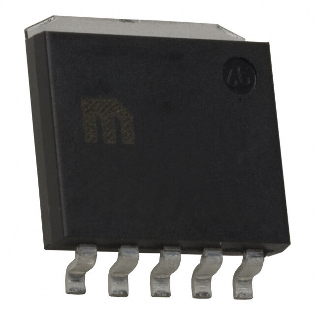
| 描述 | IC REG LDO 5V 0.4A DDPAK低压差稳压器 Auto Cat Sgl Output LDO |
| 产品分类 | |
| 品牌 | Texas Instruments |
| 产品手册 | |
| 产品图片 |
|
| rohs | 符合RoHS无铅 / 符合限制有害物质指令(RoHS)规范要求 |
| 产品系列 | 电源管理 IC,低压差稳压器,Texas Instruments TL720M05QKTTRQ1- |
| 数据手册 | |
| 产品型号 | TL720M05QKTTRQ1 |
| PCN封装 | |
| PCN设计/规格 | |
| 产品目录页面 | |
| 产品种类 | 低压差稳压器 |
| 供应商器件封装 | DDPAK/TO-263-3 |
| 其它名称 | 296-24666-1 |
| 包装 | 剪切带 (CT) |
| 单位重量 | 1.443 g |
| 商标 | Texas Instruments |
| 回动电压—最大值 | 500 mV at 300 mA |
| 安装类型 | 表面贴装 |
| 安装风格 | SMD/SMT |
| 封装 | Reel |
| 封装/外壳 | TO-263-4,D²Pak(3 引线+接片),TO-263AA |
| 封装/箱体 | TO-263-3 |
| 工作温度 | -40°C ~ 125°C |
| 工厂包装数量 | 500 |
| 最大工作温度 | + 125 C |
| 最大输入电压 | 42 V |
| 最小工作温度 | - 40 C |
| 最小输入电压 | + 5.5 V |
| 标准包装 | 1 |
| 电压-跌落(典型值) | 0.25V @ 300mA |
| 电压-输入 | 5.5 V ~ 42 V |
| 电压-输出 | 5V |
| 电压调节准确度 | 2 % |
| 电流-输出 | 400mA |
| 电流-限制(最小值) | 450mA |
| 稳压器拓扑 | 正,固定式 |
| 稳压器数 | 1 |
| 系列 | TL720M05-Q1 |
| 线路调整率 | 15 mV |
| 负载调节 | 30 mV |
| 输出电压 | 5 V |
| 输出电流 | 700 mA |
| 输出端数量 | 1 Output |
| 输出类型 | Fixed |


PDF Datasheet 数据手册内容提取
Product Sample & Technical Tools & Support & Folder Buy Documents Software Community TL720M05-Q1 SGLS380H–SEPTEMBER2008–REVISEDJULY2015 TL720M05-Q1 Low-Dropout Voltage Regulator 1 Features 3 Description • QualifiedforAutomotiveApplications The TL720M05-Q1 devices are monolithic integrated 1 low-dropout voltage regulators offered in 3-pin TO • OutputVoltageof5V ±2% packages. They regulate an input voltage up to 45 V • VeryLowCurrentConsumption to V of 5 V with 2% tolerance. The devices can OUT • VeryLowDropoutVoltage drive loads up to 450 mA and are short-circuit proof. At overtemperature, the incorporated temperature • Short-CircuitProtection protectionturnsofftheTL720M05-Q1devices. • Reverse-PolarityProtection The input capacitor (C ) compensates for line • ESDProtection> 6kV IN fluctuation. Using a resistor of approximately 1 Ω in series with C dampens the oscillation of input 2 Applications IN inductivity and input capacitance. The output • QualifiedforAutomotiveApplications capacitor (COUT) stabilizes the regulation circuit. Output is stable at C ≥ 22 μF and ESR ≤ 5 Ω, • Cluster OUT withintheoperatingtemperaturerange. • BodyControlModules The control amplifier compares a reference voltage to a voltage that is proportional to the output voltage and drives the base of the series transistor through a buffer. Saturation control as a function of the load current prevents any oversaturation of the power element. The device also incorporates a number of internalcircuitsforprotectionagainst: • Overload • Overtemperature • Reversepolarity DeviceInformation(1) PARTNUMBER PACKAGE BODYSIZE(NOM) DDPAK/TO-263(3) 10.18mm×8.41mm TL720M05-Q1 TO-252(3) 6.60mm×6.10mm HTSSOP(20) 6.50mm×4.40mm (1) For all available packages, see the orderable addendum at theendofthedatasheet. TypicalApplicationSchematic TTLL772200MM0055 VVbbaatt VVoouutt IINN OOUUTT CC11 CC22 GGNNDD 1 An IMPORTANT NOTICE at the end of this data sheet addresses availability, warranty, changes, use in safety-critical applications, intellectualpropertymattersandotherimportantdisclaimers.UNLESSOTHERWISENOTED,thisdocumentcontainsPRODUCTION DATA.
TL720M05-Q1 SGLS380H–SEPTEMBER2008–REVISEDJULY2015 www.ti.com Table of Contents 1 Features.................................................................. 1 8.3 FeatureDescription...................................................9 2 Applications........................................................... 1 8.4 DeviceFunctionalModes..........................................9 3 Description............................................................. 1 9 ApplicationandImplementation........................ 10 4 RevisionHistory..................................................... 2 9.1 ApplicationInformation............................................10 9.2 TypicalApplication .................................................10 5 PinConfigurationandFunctions......................... 3 10 PowerSupplyRecommendations..................... 12 6 Specifications......................................................... 4 11 Layout................................................................... 12 6.1 AbsoluteMaximumRatings......................................4 6.2 ESDRatings..............................................................4 11.1 LayoutGuidelines.................................................12 6.3 RecommendedOperatingConditions.......................4 11.2 LayoutExample....................................................12 6.4 ThermalInformation..................................................4 12 DeviceandDocumentationSupport................. 13 6.5 ElectricalCharacteristics...........................................5 12.1 DocumentationSupport........................................13 6.6 TypicalCharacteristics..............................................6 12.2 CommunityResources..........................................13 7 ParameterMeasurementInformation..................8 12.3 Trademarks...........................................................13 12.4 ElectrostaticDischargeCaution............................13 8 DetailedDescription.............................................. 9 12.5 Glossary................................................................13 8.1 Overview...................................................................9 13 Mechanical,Packaging,andOrderable 8.2 FunctionalBlockDiagram.........................................9 Information........................................................... 13 4 Revision History NOTE:Pagenumbersforpreviousrevisionsmaydifferfrompagenumbersinthecurrentversion. ChangesfromRevisionG(June2013)toRevisionH Page • AddedESDRatingstable,FeatureDescriptionsection,DeviceFunctionalModes,ApplicationandImplementation section,PowerSupplyRecommendationssection,Layoutsection,DeviceandDocumentationSupportsection,and Mechanical,Packaging,andOrderableInformationsection ................................................................................................. 1 ChangesfromRevisionF(May2013)toRevisionG Page • RemovedOrderingInformationtable..................................................................................................................................... 1 2 SubmitDocumentationFeedback Copyright©2008–2015,TexasInstrumentsIncorporated ProductFolderLinks:TL720M05-Q1
TL720M05-Q1 www.ti.com SGLS380H–SEPTEMBER2008–REVISEDJULY2015 5 Pin Configuration and Functions KTTPackage 3-PinTO-263 KVUPackage TopView 3-PinTO-252 TopView 3 OUT 3 OUT D D N 2 GND N 2 GND G G 1 IN 1 IN PWPPackage(1) 20-PinHTSSOPWithPowerPAD TopView NC 1 20 NC NC 2 19 IN NC 3 18 NC OUT 4 17 NC NC 5 16 NC Thermal NC 6 Pad 15 NC NC 7 14 NC GND 8 13 NC NC 9 12 NC NC 10 11 NC (1) NC-Nointernalconnection PinFunctions PIN I/O DESCRIPTION NAME TO-263 TO-252 HTSSOP Inputvoltage.Connecttogroundasclosetodeviceaspossible, IN 1 1 19 I throughaceramiccapacitor. GND 2 2 8 O Ground.Internallyconnectedtoheatsink Output.Connecttogroundwith≥22-μFcapacitor,ESR<5Ωat OUT 3 3 4 O 10kHz. 1,2,3,5,6,7, 9,10,11,12, NC — — — Notconnected 13,14,15,16, 17,18,20 Copyright©2008–2015,TexasInstrumentsIncorporated SubmitDocumentationFeedback 3 ProductFolderLinks:TL720M05-Q1
TL720M05-Q1 SGLS380H–SEPTEMBER2008–REVISEDJULY2015 www.ti.com 6 Specifications 6.1 Absolute Maximum Ratings overoperatingfree-airtemperaturerange(unlessotherwisenoted) (1) MIN MAX UNIT V Inputvoltage(2) –42 45 V I V Outputvoltage –1 40 V O T Operatingvirtual-junctiontemperature –40 150 °C J T Storagetemperature –65 150 °C stg (1) StressesbeyondthoselistedunderAbsoluteMaximumRatingsmaycausepermanentdamagetothedevice.Thesearestressratings only,andfunctionaloperationofthedeviceattheseoranyotherconditionsbeyondthoseindicatedunderRecommendedOperating Conditionsisnotimplied.Exposuretoabsolute-maximum-ratedconditionsforextendedperiodsmayaffectdevicereliability. (2) Allvoltagevaluesarewithrespecttothenetworkgroundterminal. 6.2 ESD Ratings VALUE UNIT V Electrostaticdischarge Humanbodymodel(HBM),perAECQ100-002(1) ±6000 V (ESD) (1) AECQ100-002indicatesHBMstressingisdoneinaccordancewiththeANSI/ESDA/JEDECJS-001specification. 6.3 Recommended Operating Conditions overoperatingfree-airtemperaturerange(unlessotherwisenoted) MIN NOM MAX UNIT V Inputvoltage 5.5 42 V I T Operatingfree-airtemperature –40 125 °C A T Operatingvirtual-junctiontemperature –40 150 °C J 6.4 Thermal Information TL720M05-Q1 THERMALMETRIC(1) KTT KVU PWP UNIT (TO-263) (TO-252) (HTSSOP) 3PINS 3PINS 20PINS R Junction-to-ambientthermalresistance 34.2 45.3 39.3 °C/W θJA R Junction-to-case(top)thermalresistance 38.2 36.8 22.7 °C/W θJC(top) R Junction-to-boardthermalresistance 44.9 30.8 19.1 °C/W θJB ψ Junction-to-topcharacterizationparameter 6 2.8 0.6 °C/W JT ψ Junction-to-boardcharacterizationparameter 44.5 30.2 18.9 °C/W JB R Junction-to-case(bottom)thermalresistance 0.8 0.7 1.5 °C/W θJC(bot) (1) Formoreinformationabouttraditionalandnewthermalmetrics,seetheSemiconductorandICPackageThermalMetricsapplication report,SPRA953 4 SubmitDocumentationFeedback Copyright©2008–2015,TexasInstrumentsIncorporated ProductFolderLinks:TL720M05-Q1
TL720M05-Q1 www.ti.com SGLS380H–SEPTEMBER2008–REVISEDJULY2015 6.5 Electrical Characteristics overrecommendedoperatingfree-airtemperaturerange,V =13.5V,T =−40°Cto150°C(unlessotherwisenoted) I J (seeFigure13) PARAMETER TESTCONDITIONS MIN TYP MAX UNIT I =5mAto400mA,V =6Vto28V 4.9 5 5.1 O I V Outputvoltage V O I =5mAto200mA,V =6Vto40V 4.9 5 5.1 O I I Outputcurrentlimit 450 700 950 mA O T =25°C 100 220 J I =1mA µA O Currentconsumption TJ≤85°C 100 220 I Q Iq=II−IO IO=250mA 5 10 mA I =400mA 12 22 O V Dropoutvoltage(1) I =300mA,V =V −V 250 500 mV DO O do I O Loadregulation I =5mAto400mA 15 30 mV O Lineregulation ΔV =8to32V,I =5mA –15 5 15 mV I O PSRR Power-supplyripplerejection f =100Hz,V =0.5V 60 dB r r pp (cid:1)V O Temperatureoutput-voltagedrift 0.5 mV/K (cid:1)T (1) MeasuredwhentheoutputvoltageV hasdropped100mVfromthenominalvalueobtainedatV =13.5V O I Copyright©2008–2015,TexasInstrumentsIncorporated SubmitDocumentationFeedback 5 ProductFolderLinks:TL720M05-Q1
TL720M05-Q1 SGLS380H–SEPTEMBER2008–REVISEDJULY2015 www.ti.com 6.6 Typical Characteristics 5.2 5.2 VI=6V VI=28V 5.1 5.1 V V Voltage– 4.95 Voltage– 4.95 ut ut p p ut ut –O 4.8 –O 4.8 VO VO 4.7 4.7 4.6 4.6 -45 -25 -5 15 35 55 75 95 115 135 155 -45 -25 -5 15 35 55 75 95 115 135 155 TJ–JunctionTemperature–°C TJ–JunctionTemperature–°C Figure1.OutputVoltagevsJunctionTemperature Figure2.OutputVoltagevsJunctionTemperature 12 1200 11 1100 10 1000 9 900 V A – 8 m 800 utVoltage 67 Current– 670000 utp 5 put 500 –O 4 Out 400 VO 3 I–O 300 2 200 1 100 0 0 0 1 2 3 4 5 6 7 8 9 10 -45 -25 -5 15 35 55 75 95 115 135 155 VI–InputVoltage–V TJ–JunctionTemperature–°C Figure3.OutputVoltagevsInputVoltage Figure4.OutputCurrentvsJunctionTemperature 3.5 12 3 VI= 13.5V 11 VI=13.5V –mA 2.5 –mA 190 mption 2 mption 78 Consu 1.5 Consu 56 Current 1 Current 34 I–q 0.5 I–q 2 1 0 0 0 25 50 75 100 125 150 175 200 0 50 100 150 200 250 300 350 400 IO– Output Current – mA IO–OutputCurrent–mA Figure5.CurrentConsumptionvsOutputCurrent Figure6.CurrentConsumptionvsOutputCurrent 6 SubmitDocumentationFeedback Copyright©2008–2015,TexasInstrumentsIncorporated ProductFolderLinks:TL720M05-Q1
TL720M05-Q1 www.ti.com SGLS380H–SEPTEMBER2008–REVISEDJULY2015 Typical Characteristics (continued) 800 100 700 TJ=25°C 90 VLIoNa=d1=3.15mVA V 600 80 COUT=22µF m V–DropoutVoltage–do 234500000000 RippleRejection–dB 3456700000 20 100 10 0 0 0 50 100 150 200 250 300 350 400 450 500 1.E1+001 1.1E0+002 1.E1+k03 1.1E0+k04 11.E0+00k5 IO–OutputCurrent–mA Frequency–Hz Figure7.DropoutVoltagevsOutputCurrent Figure8.Power-SupplyRippleRejectionvsFrequency 100 100 90 VIN=13.5V 90 VIN=13.5V Load=200mA Load=400mA 80 COUT=22µF 80 COUT=22µF B 70 B 70 d d RippleRejection– 34560000 RippleRejection– 34560000 20 20 10 10 0 0 1.E1+001 1.1E0+002 1.E1+k03 1.1E0+k04 11.E0+00k5 1.E1+001 1.E10+002 1.E1+k03 1.1E0+k04 11.E0+0k05 Frequency–Hz Frequency–Hz Figure9.Power-SupplyRippleRejectionvsFrequency Figure10.Power-SupplyRippleRejectionvsFrequency Unstable Region SR (Ω) Stable Region R (Ω) Stable Region E S E Unstable Region Load Capacitance (µF) Load Capacitance (µF) Figure11.ESRStabilityvsLoadCurrent Figure12.ESRStabilityvsLoadCapacitance Copyright©2008–2015,TexasInstrumentsIncorporated SubmitDocumentationFeedback 7 ProductFolderLinks:TL720M05-Q1
TL720M05-Q1 SGLS380H–SEPTEMBER2008–REVISEDJULY2015 www.ti.com 7 Parameter Measurement Information II IN OUT IO C C C I1 I2 OUT 1000 µF 100 nF 22 µF GND V V I O I GND Figure13. TestCircuit 8 SubmitDocumentationFeedback Copyright©2008–2015,TexasInstrumentsIncorporated ProductFolderLinks:TL720M05-Q1
TL720M05-Q1 www.ti.com SGLS380H–SEPTEMBER2008–REVISEDJULY2015 8 Detailed Description 8.1 Overview TheTL720M05-Q1deviceisamonolithicintegratedlow-dropoutvoltageregulatorofferedina3-pinTOpackage. The device regulates an input voltage up to 45 V to VOUT = 5 V (typical) with 2% tolerance. The device can drive loads up to 450 mA and is short-circuit proof. At overtemperature, the incorporated temperature protection turnsoffthedevice. 8.2 Functional Block Diagram Temperature Saturation Sensor Control and Protection Circuit IN OUT Bandgap Reference GND 8.3 Feature Description 8.3.1 RegulatedOutput(OUT) The OUT terminal is the regulated 5-V output. The control amplifier compares a reference voltage to a voltage that is proportional to the output voltage and drives the base of the series transistor through a buffer. Saturation control as a function of the load current prevents any oversaturation of the power element. The output has current limitation. In the event that the regulator drops out of regulation, the output tracks the input minus a drop basedontheloadcurrent. 8.4 Device Functional Modes 8.4.1 Low-VoltageTracking At low input voltages, the regulator drops out of regulation and the output voltage tracks input minus a voltage based on the load current and switch resistance. This allows for a smaller input capacitor and can possibly eliminatetheneedofusingaboostconvertorduringcold-crankconditions. Copyright©2008–2015,TexasInstrumentsIncorporated SubmitDocumentationFeedback 9 ProductFolderLinks:TL720M05-Q1
TL720M05-Q1 SGLS380H–SEPTEMBER2008–REVISEDJULY2015 www.ti.com 9 Application and Implementation NOTE Information in the following applications sections is not part of the TI component specification, and TI does not warrant its accuracy or completeness. TI’s customers are responsible for determining suitability of components for their purposes. Customers should validateandtesttheirdesignimplementationtoconfirmsystemfunctionality. 9.1 Application Information Based on the end-application, different values of external components can be used. An application can require a larger output capacitor during fast load steps to prevent a reset from occurring. TI recommends a low-ESR ceramiccapacitorwithadielectricoftypeX5RorX7Rforbetterloadtransientresponse. 9.2 Typical Application Figure14showstypicalapplicationcircuitsfortheTL720M05-Q1device. TTLL772200MM0055 VVbbaatt VVoouutt IINN OOUUTT CC11 CC22 GGNNDD Figure14. TypicalApplicationDiagram 9.2.1 DesignRequirements Forthisdesignexample,usetheparameterslistedinTable1. Table1.DesignParameters DESIGNPARAMETER EXAMPLEVALUE Inputvoltagerange 4to40V Outputvoltage 5V Outputcurrentrating 400mA Outputcapacitorrange 10to500μF OutputcapacitorESRrange 1mΩto20Ω 10 SubmitDocumentationFeedback Copyright©2008–2015,TexasInstrumentsIncorporated ProductFolderLinks:TL720M05-Q1
TL720M05-Q1 www.ti.com SGLS380H–SEPTEMBER2008–REVISEDJULY2015 9.2.2 DetailedDesignProcedure Tobeginthedesignprocess,determinethefollowing: • Inputvoltagerange • Outputvoltage • Outputcurrentrating • Outputcapacitor 9.2.2.1 ThermalConsideration Calculatethepowerdissipatedbythedeviceaccordingtothefollowingformula: P =I ×(V –V )+V xI T O I O I Q where • PT=Totalpowerdissipationofthedevice. • I =outputcurrent O • V =inputvoltage I • V =outputvoltage (1) O After determining the power dissipated by the device, calculate the junction temperature from the ambient temperatureandthedevicethermalimpedance. T =T +R xP (2) J A θJA T 9.2.3 ApplicationCurves Figure15.CH1:Vin,CH2:VoutPowerUpWaveform(Load Figure16.CH1:Vin,CH2:VoutPowerDownWaveform =50mA) (Load=50mA) Copyright©2008–2015,TexasInstrumentsIncorporated SubmitDocumentationFeedback 11 ProductFolderLinks:TL720M05-Q1
TL720M05-Q1 SGLS380H–SEPTEMBER2008–REVISEDJULY2015 www.ti.com 10 Power Supply Recommendations The device is designed to operate from an input voltage supply range between 4 V and 40 V. This input supply must be well regulated. If the input supply is located more than a few inches from the device, TI recommends addinganelectrolyticcapacitorwithavalueof47 μFandaceramicbypassattheinput. 11 Layout 11.1 Layout Guidelines DonotplaceanyofthecapacitorsontheoppositesideofthePCBfromwheretheregulatorisinstalled.Theuse of vias and long traces is strongly discouraged because of the negative impact on system performance. Vias and longtracescanalsocauseinstability. Equivalent series inductance (ESL) and ESR must be minimized to maximize performance and ensure stability. Every capacitor must be placed as close to the device as possible and on the same side of the PCB as the regulator. 11.2 Layout Example TL720M05 HTSSOP 081 NC NC NC IN Vin NC NC OUT OUT NC Input bypass capacitor Output filter NC NC capacitor NC Vin NC NC NC GND NC NC NC NC NC Figure17. LayoutExampleDiagram 12 SubmitDocumentationFeedback Copyright©2008–2015,TexasInstrumentsIncorporated ProductFolderLinks:TL720M05-Q1
TL720M05-Q1 www.ti.com SGLS380H–SEPTEMBER2008–REVISEDJULY2015 12 Device and Documentation Support 12.1 Documentation Support 12.1.1 RelatedDocumentation Forrelateddocumentation,seethefollowing: • ViewLDONoiseDemystified,SLAA412 • ViewLDOPSRRMeasurementSimplified,SLAA414 12.2 Community Resources The following links connect to TI community resources. Linked contents are provided "AS IS" by the respective contributors. They do not constitute TI specifications and do not necessarily reflect TI's views; see TI's Terms of Use. TIE2E™OnlineCommunity TI'sEngineer-to-Engineer(E2E)Community.Createdtofostercollaboration amongengineers.Ate2e.ti.com,youcanaskquestions,shareknowledge,exploreideasandhelp solveproblemswithfellowengineers. DesignSupport TI'sDesignSupport QuicklyfindhelpfulE2Eforumsalongwithdesignsupporttoolsand contactinformationfortechnicalsupport. 12.3 Trademarks E2EisatrademarkofTexasInstruments. Allothertrademarksarethepropertyoftheirrespectiveowners. 12.4 Electrostatic Discharge Caution Thesedeviceshavelimitedbuilt-inESDprotection.Theleadsshouldbeshortedtogetherorthedeviceplacedinconductivefoam duringstorageorhandlingtopreventelectrostaticdamagetotheMOSgates. 12.5 Glossary SLYZ022—TIGlossary. Thisglossarylistsandexplainsterms,acronyms,anddefinitions. 13 Mechanical, Packaging, and Orderable Information The following pages include mechanical, packaging, and orderable information. This information is the most current data available for the designated devices. This data is subject to change without notice and revision of thisdocument.Forbrowser-basedversionsofthisdatasheet,refertotheleft-handnavigation. Copyright©2008–2015,TexasInstrumentsIncorporated SubmitDocumentationFeedback 13 ProductFolderLinks:TL720M05-Q1
PACKAGE OPTION ADDENDUM www.ti.com 20-Dec-2016 PACKAGING INFORMATION Orderable Device Status Package Type Package Pins Package Eco Plan Lead/Ball Finish MSL Peak Temp Op Temp (°C) Device Marking Samples (1) Drawing Qty (2) (6) (3) (4/5) TL720M05GQKVURQ1 ACTIVE TO-252 KVU 3 2500 Green (RoHS CU SN Level-3-260C-168 HR -40 to 125 720M05Q & no Sb/Br) TL720M05QKTTRQ1 ACTIVE DDPAK/ KTT 3 500 Green (RoHS CU SN Level-3-245C-168 HR -40 to 125 T720M05Q TO-263 & no Sb/Br) TL720M05QKVURQ1 ACTIVE TO-252 KVU 3 2500 Green (RoHS CU SN Level-3-260C-168 HR -40 to 125 720M05Q & no Sb/Br) TL720M05QPWPRQ1 ACTIVE HTSSOP PWP 20 2000 Green (RoHS CU NIPDAU Level-3-260C-168 HR -40 to 125 720M05Q & no Sb/Br) (1) The marketing status values are defined as follows: ACTIVE: Product device recommended for new designs. LIFEBUY: TI has announced that the device will be discontinued, and a lifetime-buy period is in effect. NRND: Not recommended for new designs. Device is in production to support existing customers, but TI does not recommend using this part in a new design. PREVIEW: Device has been announced but is not in production. Samples may or may not be available. OBSOLETE: TI has discontinued the production of the device. (2) Eco Plan - The planned eco-friendly classification: Pb-Free (RoHS), Pb-Free (RoHS Exempt), or Green (RoHS & no Sb/Br) - please check http://www.ti.com/productcontent for the latest availability information and additional product content details. TBD: The Pb-Free/Green conversion plan has not been defined. Pb-Free (RoHS): TI's terms "Lead-Free" or "Pb-Free" mean semiconductor products that are compatible with the current RoHS requirements for all 6 substances, including the requirement that lead not exceed 0.1% by weight in homogeneous materials. Where designed to be soldered at high temperatures, TI Pb-Free products are suitable for use in specified lead-free processes. Pb-Free (RoHS Exempt): This component has a RoHS exemption for either 1) lead-based flip-chip solder bumps used between the die and package, or 2) lead-based die adhesive used between the die and leadframe. The component is otherwise considered Pb-Free (RoHS compatible) as defined above. Green (RoHS & no Sb/Br): TI defines "Green" to mean Pb-Free (RoHS compatible), and free of Bromine (Br) and Antimony (Sb) based flame retardants (Br or Sb do not exceed 0.1% by weight in homogeneous material) (3) MSL, Peak Temp. - The Moisture Sensitivity Level rating according to the JEDEC industry standard classifications, and peak solder temperature. (4) There may be additional marking, which relates to the logo, the lot trace code information, or the environmental category on the device. (5) Multiple Device Markings will be inside parentheses. Only one Device Marking contained in parentheses and separated by a "~" will appear on a device. If a line is indented then it is a continuation of the previous line and the two combined represent the entire Device Marking for that device. (6) Lead/Ball Finish - Orderable Devices may have multiple material finish options. Finish options are separated by a vertical ruled line. Lead/Ball Finish values may wrap to two lines if the finish value exceeds the maximum column width. Addendum-Page 1
PACKAGE OPTION ADDENDUM www.ti.com 20-Dec-2016 Important Information and Disclaimer:The information provided on this page represents TI's knowledge and belief as of the date that it is provided. TI bases its knowledge and belief on information provided by third parties, and makes no representation or warranty as to the accuracy of such information. Efforts are underway to better integrate information from third parties. TI has taken and continues to take reasonable steps to provide representative and accurate information but may not have conducted destructive testing or chemical analysis on incoming materials and chemicals. TI and TI suppliers consider certain information to be proprietary, and thus CAS numbers and other limited information may not be available for release. In no event shall TI's liability arising out of such information exceed the total purchase price of the TI part(s) at issue in this document sold by TI to Customer on an annual basis. Addendum-Page 2
PACKAGE MATERIALS INFORMATION www.ti.com 20-Feb-2019 TAPE AND REEL INFORMATION *Alldimensionsarenominal Device Package Package Pins SPQ Reel Reel A0 B0 K0 P1 W Pin1 Type Drawing Diameter Width (mm) (mm) (mm) (mm) (mm) Quadrant (mm) W1(mm) TL720M05GQKVURQ1 TO-252 KVU 3 2500 330.0 16.4 6.9 10.5 2.7 8.0 16.0 Q2 TL720M05QKVURQ1 TO-252 KVU 3 2500 330.0 16.4 6.9 10.5 2.7 8.0 16.0 Q2 TL720M05QPWPRQ1 HTSSOP PWP 20 2000 330.0 16.4 6.95 7.1 1.6 8.0 16.0 Q1 PackMaterials-Page1
PACKAGE MATERIALS INFORMATION www.ti.com 20-Feb-2019 *Alldimensionsarenominal Device PackageType PackageDrawing Pins SPQ Length(mm) Width(mm) Height(mm) TL720M05GQKVURQ1 TO-252 KVU 3 2500 340.0 340.0 38.0 TL720M05QKVURQ1 TO-252 KVU 3 2500 340.0 340.0 38.0 TL720M05QPWPRQ1 HTSSOP PWP 20 2000 350.0 350.0 43.0 PackMaterials-Page2
None
None
None
None
None
None
PACKAGE OUTLINE KVU0003A TO-252 - 2.52 mm max height SCALE 1.500 TO-252 10.41 9.40 6.22 1.27 B A 5.97 0.89 1 2.29 6.70 2 5.460 6.35 4.58 4.953 3 0.890 3X 1.02 0.635 OPTIONAL NOTE 3 0.61 0.25 C A B 0.61 2.52 MAX C 0.46 0.61 0.46 SEE DETAIL A 5.21 MIN 3 4.32 2 4 MIN 1 EXPOSED 0.51 THERMAL PAD GAGE PLANE NOTE 3 0.13 0 -8 1.78 0.00 1.40 DETA 7.000AIL A TYPICAL 4218915/A 02/2017 NOTES: 1. All linear dimensions are in millimeters. Any dimensions in parenthesis are for reference only. Dimensioning and tolerancing per ASME Y14.5M. 2. This drawing is subject to change without notice. 3. Shape may vary per different assembly sites. 4. Reference JEDEC registration TO-252. www.ti.com
EXAMPLE BOARD LAYOUT KVU0003A TO-252 - 2.52 mm max height TO-252 2X (2.75) (6.15) 2X (1) 1 4 SYMM (4.58) (5.55) 3 (R0.05) TYP (4.2) (2.5) PKG LAND PATTERN EXAMPLE EXPOSED METAL SHOWN SCALE:6X 0.07 MAX 0.07 MIN ALL AROUND ALL AROUND EXPOSED METAL EXPOSED METAL SOLDER MASK METAL METAL UNDER SOLDER MASK OPENING SOLDER MASK OPENING NON SOLDER MASK SOLDER MASK DEFINED DEFINED SOLDER MASK DETAILS NOT TO SCALE 4218915/A 02/2017 NOTES: (continued) 5. This package is designed to be soldered to a thermal pad on the board. For more information, see Texas Instruments literature numbers SLMA002(www.ti.com/lit/slm002) and SLMA004 (www.ti.com/lit/slma004). 6. Vias are optional depending on application, refer to device data sheet. It is recommended that vias under paste be filled, plugged or tented. www.ti.com
EXAMPLE STENCIL DESIGN KVU0003A TO-252 - 2.52 mm max height TO-252 (1.18) TYP 2X (2.75) 2X (1) (0.14) 1 (R0.05) (1.33) TYP SYMM (4.58) 4 3 20X (1.13) (4.2) 20X (0.98) PKG SOLDER PASTE EXAMPLE BASED ON 0.125 mm THICK STENCIL EXPOSED PAD 65% PRINTED SOLDER COVERAGE BY AREA SCALE:8X 4218915/A 02/2017 NOTES: (continued) 7. Laser cutting apertures with trapezoidal walls and rounded corners may offer better paste release. IPC-7525 may have alternate design recommendations. 8. Board assembly site may have different recommendations for stencil design. www.ti.com
IMPORTANTNOTICEANDDISCLAIMER TIPROVIDESTECHNICALANDRELIABILITYDATA(INCLUDINGDATASHEETS),DESIGNRESOURCES(INCLUDINGREFERENCE DESIGNS),APPLICATIONOROTHERDESIGNADVICE,WEBTOOLS,SAFETYINFORMATION,ANDOTHERRESOURCES“ASIS” ANDWITHALLFAULTS,ANDDISCLAIMSALLWARRANTIES,EXPRESSANDIMPLIED,INCLUDINGWITHOUTLIMITATIONANY IMPLIEDWARRANTIESOFMERCHANTABILITY,FITNESSFORAPARTICULARPURPOSEORNON-INFRINGEMENTOFTHIRD PARTYINTELLECTUALPROPERTYRIGHTS. TheseresourcesareintendedforskilleddevelopersdesigningwithTIproducts.Youaresolelyresponsiblefor(1)selectingtheappropriate TIproductsforyourapplication,(2)designing,validatingandtestingyourapplication,and(3)ensuringyourapplicationmeetsapplicable standards,andanyothersafety,security,orotherrequirements.Theseresourcesaresubjecttochangewithoutnotice.TIgrantsyou permissiontousetheseresourcesonlyfordevelopmentofanapplicationthatusestheTIproductsdescribedintheresource.Other reproductionanddisplayoftheseresourcesisprohibited.NolicenseisgrantedtoanyotherTIintellectualpropertyrightortoanythird partyintellectualpropertyright.TIdisclaimsresponsibilityfor,andyouwillfullyindemnifyTIanditsrepresentativesagainst,anyclaims, damages,costs,losses,andliabilitiesarisingoutofyouruseoftheseresources. TI’sproductsareprovidedsubjecttoTI’sTermsofSale(www.ti.com/legal/termsofsale.html)orotherapplicabletermsavailableeitheron ti.comorprovidedinconjunctionwithsuchTIproducts.TI’sprovisionoftheseresourcesdoesnotexpandorotherwisealterTI’sapplicable warrantiesorwarrantydisclaimersforTIproducts. MailingAddress:TexasInstruments,PostOfficeBox655303,Dallas,Texas75265 Copyright©2019,TexasInstrumentsIncorporated