ICGOO在线商城 > 集成电路(IC) > PMIC - LED 驱动器 > TL4242DRJR
 Datasheet下载
- 型号: TL4242DRJR
- 制造商: Texas Instruments
- 库位|库存: xxxx|xxxx
- 要求:
| 数量阶梯 | 香港交货 | 国内含税 |
| +xxxx | $xxxx | ¥xxxx |
查看当月历史价格
查看今年历史价格
TL4242DRJR产品简介:
ICGOO电子元器件商城为您提供TL4242DRJR由Texas Instruments设计生产,在icgoo商城现货销售,并且可以通过原厂、代理商等渠道进行代购。 TL4242DRJR价格参考。Texas InstrumentsTL4242DRJR封装/规格:PMIC - LED 驱动器, LED 驱动器 IC 1 输出 线性 500mA 8-SON(4x4)。您可以下载TL4242DRJR参考资料、Datasheet数据手册功能说明书,资料中有TL4242DRJR 详细功能的应用电路图电压和使用方法及教程。
Texas Instruments(德州仪器)的TL4242DRJR是一款PMIC - LED驱动器,主要用于驱动高亮度LED(HB-LED)的应用场景。以下是其典型应用场景及特点:

 1. 汽车照明
   - 前照灯:TL4242DRJR可以用于驱动汽车前照灯中的LED光源,提供稳定的电流输出,确保亮度一致。
   - 日间行车灯(DRL):支持日间行车灯的高效驱动,提高能效并延长LED寿命。
   - 雾灯和转向灯:适用于低功耗、高效率的LED驱动需求。

 2. 工业照明
   - 户外照明:如街道灯、停车场灯等,需要高可靠性和宽工作温度范围的应用。
   - 标志和信号灯:为交通信号灯、广告牌等提供稳定电流,确保长时间运行。

 3. 消费电子
   - 背光显示:用于驱动LCD显示屏的背光LED,常见于电视、显示器和笔记本电脑。
   - 便携设备:如手电筒、相机闪光灯等,提供高效的电源管理。

 4. 特点与优势
   - 高效率:采用同步整流技术,实现高达95%以上的转换效率。
   - 宽输入电压范围:支持4.5V至60V的输入电压,适合多种电源环境。
   - 可调输出电流:通过外部电阻设置LED电流,灵活适应不同功率的LED。
   - 保护功能:内置过温保护、短路保护和过压保护,增强系统可靠性。
   - 小型封装:采用DRJ封装,节省PCB空间,便于紧凑设计。

 5. 其他应用
   - 建筑照明:如景观灯、室内装饰灯等,提供节能环保的解决方案。
   - 应急照明:在断电情况下,驱动备用LED光源。

总之,TL4242DRJR凭借其高效能、高可靠性和灵活性,广泛应用于汽车、工业和消费类领域的LED驱动需求中。
| 参数 | 数值 |
| 产品目录 | 集成电路 (IC)光电子产品 |
| 描述 | IC LED DRIVER PWM CONTROL 8-SONLED照明驱动器 Adj LED DRIVER |
| 产品分类 | |
| 品牌 | Texas Instruments |
| 产品手册 | |
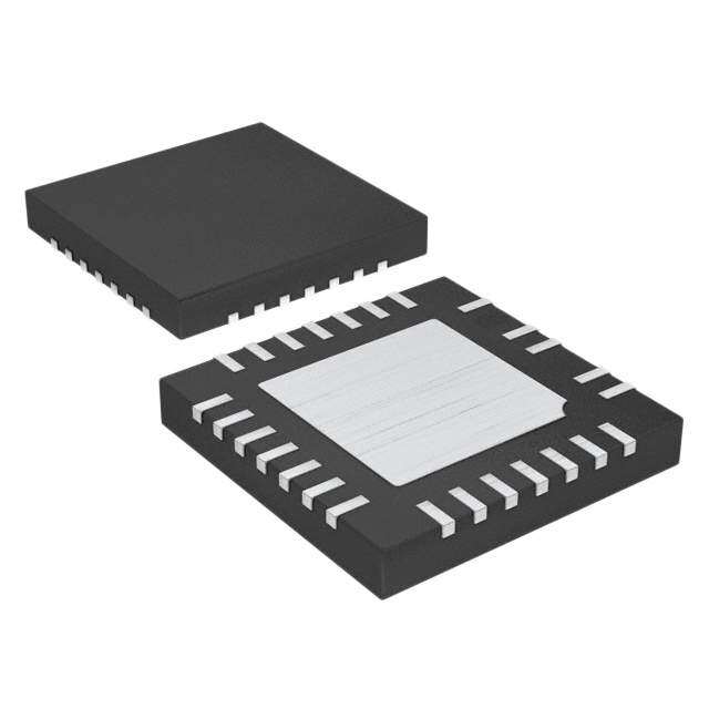
| 产品图片 |
|
| rohs | 符合RoHS无铅 / 符合限制有害物质指令(RoHS)规范要求 |
| 产品系列 | LED照明电子器件,LED照明驱动器,Texas Instruments TL4242DRJR- |
| 数据手册 | |
| 产品型号 | TL4242DRJR |
| PCN设计/规格 | |
| 产品目录页面 | |
| 产品种类 | LED照明驱动器 |
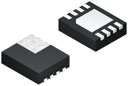
| 供应商器件封装 | 8-SON 裸露焊盘(4x4) |
| 其它名称 | 296-23615-1 |
| 内部驱动器 | 是 |
| 包装 | 剪切带 (CT) |
| 参考设计库 | http://www.digikey.com/rdl/4294959899/4294959898/412 |
| 商标 | Texas Instruments |
| 安装类型 | 表面贴装 |
| 安装风格 | SMD/SMT |
| 封装 | Reel |
| 封装/外壳 | 8-WDFN 裸露焊盘 |
| 封装/箱体 | WSON-8 |
| 工作温度 | -40°C ~ 150°C |
| 工厂包装数量 | 1000 |
| 恒压 | - |
| 恒流 | 是 |
| 拓扑 | 线性(LDO),PWM |
| 拓扑结构 | PWM |
| 最大工作温度 | + 85 C |
| 最大电源电流 | 22 mA |
| 最小工作温度 | - 40 C |
| 标准包装 | 1 |
| 特色产品 | http://www.digikey.com/cn/zh/ph/Texas-Instruments/tl4242.html |
| 电压-电源 | 4.5 V ~ 42 V |
| 电压-输出 | 3.8 V ~ 41.3 V |
| 类型 | Linear |
| 类型-初级 | 车载 |
| 类型-次级 | - |
| 系列 | TL4242 |
| 输入电压 | 4.5 V to 42 V |
| 输出数 | 1 |
| 输出电流 | 500 mA |
| 输出端数量 | 1 Output |
| 输出类型 | Current Mode |
| 频率 | - |


- 商务部:美国ITC正式对集成电路等产品启动337调查
- 曝三星4nm工艺存在良率问题 高通将骁龙8 Gen1或转产台积电
- 太阳诱电将投资9.5亿元在常州建新厂生产MLCC 预计2023年完工
- 英特尔发布欧洲新工厂建设计划 深化IDM 2.0 战略
- 台积电先进制程称霸业界 有大客户加持明年业绩稳了
- 达到5530亿美元!SIA预计今年全球半导体销售额将创下新高
- 英特尔拟将自动驾驶子公司Mobileye上市 估值或超500亿美元
- 三星加码芯片和SET,合并消费电子和移动部门,撤换高东真等 CEO
- 三星电子宣布重大人事变动 还合并消费电子和移动部门
- 海关总署:前11个月进口集成电路产品价值2.52万亿元 增长14.8%


PDF Datasheet 数据手册内容提取
Product Sample & Technical Tools & Support & Folder Buy Documents Software Community TL4242 SLVS641B–APRIL2008–REVISEDMARCH2015 TL4242 500-mA, Adjustable, Constant-Current LED Driver 1 Features 3 Description • AdjustableConstantCurrentupto500mA(±5%) The TL4242 device is an integrated, adjustable, 1 constant-current source that can drive loads up to • PWMBrightnessRegulation 500 mA. The output current level can be adjusted • WideInputVoltageRangeupto42V through an external resistor. The device is designed • LowDropVoltage to supply high-power LEDs. The TL4242 is provided in the DRJ (WSON) package. Protection circuits • Open-LoadDetection prevent damage to the device in case of overload, • OvertemperatureProtection short circuit, reverse polarity, and overtemperature. • Short-CircuitProof The connected LEDs are protected against reverse polarityaswellasexcessvoltagesupto45V. • Reverse-PolarityProof • WideTemperatureRange:–40°Cto150°C The integrated PWM input of the TL4242 permits LED brightness regulation by pulse-width modulation 2 Applications (PWM). Due to the high input impedance of the PWM input, the LED driver can be operated as a protected • Signage high-sideswitch. • IndustrialLighting The TL4242 is characterized for operation from • Printers –40°Cto150°C. DeviceInformation(1) PARTNUMBER PACKAGE BODYSIZE(NOM) TL4242 WSON(8) 4.00mm×4.00mm (1) For all available packages, see the orderable addendum at theendofthedatasheet. SimplifiedSchematic Microcontroller ST PWM Power Supply or I Q Battery TL4242 REF GND D 1 An IMPORTANT NOTICE at the end of this data sheet addresses availability, warranty, changes, use in safety-critical applications, intellectualpropertymattersandotherimportantdisclaimers.PRODUCTIONDATA.
TL4242 SLVS641B–APRIL2008–REVISEDMARCH2015 www.ti.com Table of Contents 1 Features.................................................................. 1 7.3 FeatureDescription...................................................7 2 Applications........................................................... 1 7.4 DeviceFunctionalModes..........................................8 3 Description............................................................. 1 8 ApplicationandImplementation.......................... 9 4 RevisionHistory..................................................... 2 8.1 ApplicationInformation..............................................9 8.2 TypicalApplication..................................................10 5 PinConfigurationandFunctions......................... 3 9 PowerSupplyRecommendations...................... 12 6 Specifications......................................................... 3 10 Layout................................................................... 12 6.1 AbsoluteMaximumRatings......................................3 6.2 ESDRatings..............................................................4 10.1 LayoutGuidelines.................................................12 6.3 RecommendedOperatingConditions.......................4 10.2 LayoutExample....................................................12 6.4 ThermalInformation..................................................4 11 DeviceandDocumentationSupport................. 13 6.5 ElectricalCharacteristics...........................................4 11.1 Trademarks...........................................................13 6.6 TypicalCharacteristics..............................................6 11.2 ElectrostaticDischargeCaution............................13 7 DetailedDescription.............................................. 7 11.3 Glossary................................................................13 7.1 Overview...................................................................7 12 Mechanical,Packaging,andOrderable Information........................................................... 13 7.2 FunctionalBlockDiagram.........................................7 4 Revision History ChangesfromRevisionA(April2011)toRevisionB Page • AddedESDRatingstable,FeatureDescriptionsection,DeviceFunctionalModes,ApplicationandImplementation section,PowerSupplyRecommendationssection,Layoutsection,DeviceandDocumentationSupportsection,and Mechanical,Packaging,andOrderableInformationsection. ................................................................................................ 1 2 SubmitDocumentationFeedback Copyright©2008–2015,TexasInstrumentsIncorporated ProductFolderLinks:TL4242
TL4242 www.ti.com SLVS641B–APRIL2008–REVISEDMARCH2015 5 Pin Configuration and Functions DRJPackage 8-PinWSON (TopView) PWM 1 8 I ST 2 Exposed 7 NC Thermal GND 3 Pad 6 Q REF 4 5 D NC–No internal connection PinFunctions PIN I/O DESCRIPTION NO. NAME 1 PWM I Pulse-widthmodulationinput.Ifnotused,connecttoI. 2 ST O Statusoutput.Open-collectoroutput.Connecttoanexternalpullupresistor(R ≥4.7kΩ). PULLUP 3 GND — Ground 4 REF I Referenceinput.Connecttoashuntresistor. Statusdelay.Tosetstatusreactiondelay,connecttoGNDwithacapacitor.Ifnodelayisneeded,leave 5 D I open. 6 Q O Output 7 NC — Nointernalconnection 8 I I Input.ConnectdirectlytoGNDascloseaspossibletothedevicewitha100-nFceramiccapacitor. Thermal — — ThethermalpadmustbesoldereddirectlytothePCB.Itmaybeconnectedtogroundorleftfloating. Pad 6 Specifications 6.1 Absolute Maximum Ratings overoperatingfree-airtemperaturerange(unlessotherwisenoted)(1) MIN MAX UNIT V Supplyvoltage(2) –42 45 V CC D –0.3 7 V Inputvoltage PWM –40 40 V I REF –1 16 Q –1 41 V Outputvoltage V O ST –0.3 40 PWM ±1 I Outputcurrent REF ±2 mA O ST ±5 T Virtual-junctiontemperature –40 150 °C J T Storagetemperature –50 150 °C stg (1) StressesbeyondthoselistedunderAbsoluteMaximumRatingsmaycausepermanentdamagetothedevice.Thesearestressratings only,andfunctionaloperationofthedeviceattheseoranyotherconditionsbeyondthoseindicatedunderRecommendedOperating Conditionsisnotimplied.Exposuretoabsolute-maximum-ratedconditionsforextendedperiodsmayaffectdevicereliability. (2) Allvoltagevaluesarewithrespecttothenetworkgroundterminal. Copyright©2008–2015,TexasInstrumentsIncorporated SubmitDocumentationFeedback 3 ProductFolderLinks:TL4242
TL4242 SLVS641B–APRIL2008–REVISEDMARCH2015 www.ti.com 6.2 ESD Ratings VALUE UNIT Human-bodymodel(HBM),perANSI/ESDA/JEDECJS-001(1) ±1000 V(ESD) Electrostaticdischarge Charged-devicemodel(CDM),perJEDECspecificationJESD22- ±1000 V C101(2) (1) JEDECdocumentJEP155statesthat500-VHBMallowssafemanufacturingwithastandardESDcontrolprocess. (2) JEDECdocumentJEP157statesthat250-VCDMallowssafemanufacturingwithastandardESDcontrolprocess. 6.3 Recommended Operating Conditions MIN MAX UNIT V Supplyvoltage 4.5 42 V CC V Status(ST)outputvoltage 16 V ST V PWMvoltage 0 40 V PWM C Statusdelay(D)capacitance 0 2.2 μF D R Reference(REF)resistor 0 10 Ω REF T Virtual-junctiontemperature –40 150 °C J 6.4 Thermal Information TL4242 THERMALMETRIC(1) DRJ(WSON) UNIT 8PINS R Junction-to-ambientthermalresistance 39.0 θJA R Junction-to-case(top)thermalresistance 31.5 θJC(top) R Junction-to-boardthermalresistance 15.5 θJB °C/W ψ Junction-to-topcharacterizationparameter 0.3 JT ψ Junction-to-boardcharacterizationparameter 15.6 JB R Junction-to-case(bottom)thermalresistance 1.8 θJC(bot) (1) Formoreinformationabouttraditionalandnewthermalmetrics,seetheICPackageThermalMetricsapplicationreport,SPRA953. 6.5 Electrical Characteristics overrecommendedoperatingfree-airtemperaturerange,V =13.5V,R =0.47Ω,V ,T =–40°Cto150°C,all I REF PWM,H J voltageswithrespecttoground(unlessotherwisenoted) PARAMETER TESTCONDITIONS MIN TYP MAX UNIT I Supplycurrent V =6.6V 12 22 mA qL Q I Supplycurrent,offmode PWM=L,T <85°C 0.1 2 μA qOFF J OUTPUTELECTRICALCHARACTERISTICS V –V (1)=6.6V 357 376 395 Q REF V –V =6.6V,R =1Ω 168 177 185 Q REF REF IQ Outputcurrent VQ–VREF=6.6V,RREF=0.39Ω 431 454 476 mA V –V =5.4Vto7.8V,V =9 Q REF I 357 376 395 Vto16V I Outputcurrentlimit R =0Ω 600 mA Qmax REF V Dropvoltage I =300mA 0.35 0.7 V dr Q PWMINPUTELECTRICALCHARACTERISTICS V PWM, High-levelPWMvoltage 2.6 V H V PWM, Low-levelPWMvoltage 0.7 V L I High-levelPWMinputcurrent V =5V 220 500 μA PWM,H PWM I Low-levelPWMinputcurrent V =0V –1 1 μA PWM,L PWM (1) V –V equalstheforwardvoltagesumoftheconnectedLEDs(seeFigure3). Q REF 4 SubmitDocumentationFeedback Copyright©2008–2015,TexasInstrumentsIncorporated ProductFolderLinks:TL4242
TL4242 www.ti.com SLVS641B–APRIL2008–REVISEDMARCH2015 Electrical Characteristics (continued) overrecommendedoperatingfree-airtemperaturerange,V =13.5V,R =0.47Ω,V ,T =–40°Cto150°C,all I REF PWM,H J voltageswithrespecttoground(unlessotherwisenoted) PARAMETER TESTCONDITIONS MIN TYP MAX UNIT t PWM,O Delaytime,turnon 70%ofI ,SeeFigure5 0 15 40 μs Qnom N t PWM,O Delaytime,turnoff 30%ofI ,SeeFigure5 0 15 40 μs Qnom FF REFERENCE(REF)ELECTRICALCHARACTERISTICS V Referencevoltage R =0.39Ωto1Ω 168 177 185 mV REF REF I Referenceinputcurrent V =180mV –1 0.1 1 μA REF REF STATUSOUTPUT(ST)ELECTRICALCHARACTERISTICS V Lowerstatus-switchingthreshold ST=L 15 25 mV IQL V Upperstatus-switchingthreshold ST=H 30 40 mV IQH V Low-levelstatusvoltage I =1.5mA 0.4 V STL ST I Leakagecurrent V =5V 5 μA STLK ST STATUSDELAY(D)ELECTRICALCHARACTERISTICS t Delaytime,statusreaction C =47nF,STH→L 6 10 14 ms STHL D t Delaytime,statusrelease C =47nF,STL→H 10 20 μs STLH D Copyright©2008–2015,TexasInstrumentsIncorporated SubmitDocumentationFeedback 5 ProductFolderLinks:TL4242
TL4242 SLVS641B–APRIL2008–REVISEDMARCH2015 www.ti.com 6.6 Typical Characteristics 700 450 400 600 350 mA 500 mA 300 – – Current 400 Current 220500 ut ut utp 300 utp 150 O O – – 100 IOUT 200 IOUT 50 100 0 -50 0 0 5 10 15 20 25 30 35 40 0 0.25 0.5 0.75 1 1.25 1.5 1.75 2 2.25 RREF–8W VCC–SupplyVoltage–V Figure1.OutputCurrentvsExternalResistor Figure2.OutputCurrentvsSupplyVoltage 178.5 60 50 178.0 V m A 40 – 177.5 µ ge – Volta rrent 30 u ce 177.0 C n M re W 20 Refe 176.5 –P – WM 10 F P E I R V 176.0 0 175.5 -10 -40 -20 0 20 40 60 80 100 120 140 0 10 20 30 40 T –VirtualJunctionTemperature–°C V –PWMVoltage–V J PWM Figure3.ReferenceVoltagevsJunctionTemperature Figure4.PWMPinInputCurrentvsPWMVoltage 6 SubmitDocumentationFeedback Copyright©2008–2015,TexasInstrumentsIncorporated ProductFolderLinks:TL4242
TL4242 www.ti.com SLVS641B–APRIL2008–REVISEDMARCH2015 7 Detailed Description 7.1 Overview The TL4242 device is an integrated, adjustable, constant-current source that can drive loads up to 500 mA. The output current level can be adjusted through an external resistor. The device is designed to supply high-power LEDs. Protection circuits prevent damage to the device in case of overload, short circuit, reverse polarity, and overtemperature.TheconnectedLEDsareprotectedagainstreversepolarityaswellasexcessvoltagesupto45 V. The integrated PWM input of the TL4242 permits LED brightness regulation by pulse-width modulation (PWM). Due to the high input impedance of the PWM input, the LED driver can be operated as a protected high- sideswitch. 7.2 Functional Block Diagram 8 6 I Q Bias Supply 1 PWM + − Bandgap Reference 4 REF Comparator 2 ST Status Delay 3 5 GND D 7.3 Feature Description 7.3.1 PWMInput The integrated PWM input of the TL4242 permits LED brightness regulation by pulse-width modulation (PWM). The overall LED brightness is a function of the shunt resistor, R , and the PWM duty cycle. The PWM input REF can also function as a simple enable control. When the PWM input is below V , the device will go to a low- PWM,L power consumption sleep mode. Due to the high input impedance of the PWM input, the LED driver can be operatedasaprotectedhigh-sideswitch. The LEDs are driven by a supply current that is adjusted by the resistor, R , preventing brightness variations REF due to forward voltage spread of the LEDs. The luminosity spread arising from the LED production process can be compensated through software by an appropriate duty cycle applied to the PWM pin. Therefore, it is not necessarytoselectLEDsforforwardvoltageorluminosityclasses. 7.3.2 STOutput The status output of the LED driver (ST) detects an open-load condition, enabling supervision of correct LED operation. An LED failure is detected as a voltage drop at the shunt resistor (R ) below 25 mV (typical). In this REF case, the status output pin (ST) is set low after a delay time adjustable by an optional capacitor connected to pinD. Copyright©2008–2015,TexasInstrumentsIncorporated SubmitDocumentationFeedback 7 ProductFolderLinks:TL4242
TL4242 SLVS641B–APRIL2008–REVISEDMARCH2015 www.ti.com Feature Description (continued) 7.3.2.1 FunctionandTimingDiagram The functionality and timing of ST and PWM are shown in Figure 5. The status delay can be adjusted through thecapacitorconnectedtopinD.Delaytimescaleslinearlywithcapacitance,C : D C t (cid:2) D (cid:1)10ms STHL,typ 47nF (1) C t (cid:2) D (cid:1)10(cid:1)s STLH,typ 47nF (2) V Open Open PWM Load Load V PWM,H V PWM,L I t Q t PWM,ON t I PWM,OFF Q,nom 70% 30% t V D t STHL V LD t V ST t Figure5. FunctionandTimingDiagram 7.4 Device Functional Modes Table1.FunctionalModes V DEVICEMODE PWM High Active Low Sleep 8 SubmitDocumentationFeedback Copyright©2008–2015,TexasInstrumentsIncorporated ProductFolderLinks:TL4242
TL4242 www.ti.com SLVS641B–APRIL2008–REVISEDMARCH2015 8 Application and Implementation NOTE Information in the following applications sections is not part of the TI component specification, and TI does not warrant its accuracy or completeness. TI’s customers are responsible for determining suitability of components for their purposes. Customers should validateandtesttheirdesignimplementationtoconfirmsystemfunctionality. 8.1 Application Information 8.1.1 InputSupplyVoltage The input supply voltage calculates as the sum of the LED forward voltages, the TL4242 drop voltage, and the voltage drop across the shunt resistor, R . The total LED forward voltage depends on the type of LED and the REF number of LEDs in the string. The TL4242 drop voltage must be greater than V (typically 350 mV), but must not dr be too high as this could cause excessive power dissipation inside the device. The voltage drop across the shunt resistoristypically177mV. 8.1.2 PowerDissipationinTL4242 PowerdissipationintheTL4242willcomefromtwosources: • Quiescentpower:(Inputvoltage ×Supplycurrent) • Powerdissipationinthepasselement: ((V –V )×I ) (3) I Q Q The power dissipation in the pass element can be significant if the input voltage, V, is much higher than V . The I Q power dissipation is also dependent on the LED current. Equation 4 is an example calculation using the design parameterslistedinTable2. Table2.DesignParameters DESIGNPARAMETER EXAMPLEVALUE V 13.5V I V 7V Q I 0.2A Q ((V –V )×I )=(13.5–7)×0.2=1.3W (4) I Q Q In Equation 4, there is 1.3 W of power dissipation in the pass element of the TL4242. This power dissipation will cause the junction temperature of the device to increase. The increase in temperature is equal to R × 1.3 W. θJA PleasenotethatR isdependentonthePCBlayout. θJA 8.1.3 SettingtheOutputCurrent An external shunt resistor in the ground path of the connected LEDs is used to sense the LED current. A regulation loop holds the voltage drop at the shunt resistor at a constant level of 177 mV (typical). The constant- current level can be adjusted by selecting the shunt resistance, R . Calculate the typical output current using REF theequation: I =V /R Q,typ REF REF where • V isthereferencevoltage(typically177mV)(seeElectricalCharacteristics). (5) REF TheequationappliesforR =0.39 Ωto10 Ω. REF TheoutputcurrentisshownasafunctionofthereferenceresistanceinFigure1. Copyright©2008–2015,TexasInstrumentsIncorporated SubmitDocumentationFeedback 9 ProductFolderLinks:TL4242
TL4242 SLVS641B–APRIL2008–REVISEDMARCH2015 www.ti.com 8.2 Typical Application Figure6 showsatypicalapplicationwiththeTL4242drivingthreeLEDsinseries. VBAT I RO SI Microcontroller Q RADJ GND D 10 µF 10 kΩ 100 nF ST PWM I Q TL4242 REF LED Dragon GND D 47 nF 0.47Ω 0.25W RREF Figure6. ApplicationCircuit 8.2.1 DesignRequirements Forthisdesignexample,usethefollowingastheinputparametersinTable3. Table3.DesignParameters DESIGNPARAMETERS EXAMPLEVALUE #ofLEDs 3 ForwardVoltageofeachLED 3.5V LEDCurrent 377mA 8.2.2 DetailedDesignProcedure 8.2.2.1 InputVoltage The input voltage must be greater than the sum of the LED forward voltages, the TL4242 drop voltage, and the voltage drop across the shunt resistor, R . In this design example, the total LED forward voltage is 3 × 3.5 V = REF 10.5V.ThetypicalTL4242dropvoltageis350mV.Thetypicalvoltagedropacrosstheshuntresistoris177mV. In sum, the input voltage must be greater than 10.5 + 0.350 + 0.177 = 11.027 V. An appropriate input voltage for thisapplicationwouldbe12V. 8.2.2.2 ShuntResistor Theshuntresistorvalue,R ,canbecalculatedbasedonthedesiredLEDcurrent. REF I =V /R Q,typ REF REF where • V isthereferencevoltage(typically177mV)(seeElectricalCharacteristics). (6) REF As shown in Design Requirements, the desired LED current is 377 mA. The appropriate R value for this REF applicationcalculatestobe0.47Ω. 10 SubmitDocumentationFeedback Copyright©2008–2015,TexasInstrumentsIncorporated ProductFolderLinks:TL4242
TL4242 www.ti.com SLVS641B–APRIL2008–REVISEDMARCH2015 8.2.3 ApplicationCurve 700 600 A 500 m – nt e 400 rr u C ut p 300 ut O – T 200 U O I 100 0 0 0.25 0.5 0.75 1 1.25 1.5 1.75 2 2.25 R –8W REF Figure7. OutputCurrentvsExternalResistor Copyright©2008–2015,TexasInstrumentsIncorporated SubmitDocumentationFeedback 11 ProductFolderLinks:TL4242
TL4242 SLVS641B–APRIL2008–REVISEDMARCH2015 www.ti.com 9 Power Supply Recommendations The input voltage at the I pin must be greater than the sum of the LED forward voltages, the voltage drop across the TL4242 (from I to Q), and the voltage drop across the shunt resistor R . For an example of this calculation, REF refer to Typical Application. The input voltage should not exceed the recommended maximum operation voltage of42V. 10 Layout 10.1 Layout Guidelines The REF pin should be routed directly to the shunt resistor, R . If there is a long PCB trace between the LED REF stringandtheshuntresistor,theREFpinshouldconnectclosetotheshuntresistor(ratherthanclosetotheLED string)toallowforaccuratesensingacrosstheshuntresistor. The traces for I and Q will carry the full LED current. These traces should be the appropriate width to carry the LEDcurrent. The exposed thermal pad on the bottom of the TL4242 should be connected to the PCB. The thermal pad helps to dissipate heat in the case of high power dissipation in the device. To further enhance the thermal performance ofthedevice,thethermalpadcanbeconnectedbyviastothegroundlayerinthePCB. 10.2 Layout Example To µC PWM I To power supply To µC ST NC GND Q To pullup source REF D R REF Via to GND Plane Figure8. PCBLayout 12 SubmitDocumentationFeedback Copyright©2008–2015,TexasInstrumentsIncorporated ProductFolderLinks:TL4242
TL4242 www.ti.com SLVS641B–APRIL2008–REVISEDMARCH2015 11 Device and Documentation Support 11.1 Trademarks Alltrademarksarethepropertyoftheirrespectiveowners. 11.2 Electrostatic Discharge Caution Thesedeviceshavelimitedbuilt-inESDprotection.Theleadsshouldbeshortedtogetherorthedeviceplacedinconductivefoam duringstorageorhandlingtopreventelectrostaticdamagetotheMOSgates. 11.3 Glossary SLYZ022—TIGlossary. Thisglossarylistsandexplainsterms,acronyms,anddefinitions. 12 Mechanical, Packaging, and Orderable Information The following pages include mechanical, packaging, and orderable information. This information is the most current data available for the designated devices. This data is subject to change without notice and revision of thisdocument.Forbrowser-basedversionsofthisdatasheet,refertotheleft-handnavigation. Copyright©2008–2015,TexasInstrumentsIncorporated SubmitDocumentationFeedback 13 ProductFolderLinks:TL4242
PACKAGE OPTION ADDENDUM www.ti.com 23-Nov-2017 PACKAGING INFORMATION Orderable Device Status Package Type Package Pins Package Eco Plan Lead/Ball Finish MSL Peak Temp Op Temp (°C) Device Marking Samples (1) Drawing Qty (2) (6) (3) (4/5) TL4242DRJR ACTIVE SON DRJ 8 3000 Green (RoHS CU NIPDAU Level-3-260C-168 HR -40 to 125 T4242 & no Sb/Br) (1) The marketing status values are defined as follows: ACTIVE: Product device recommended for new designs. LIFEBUY: TI has announced that the device will be discontinued, and a lifetime-buy period is in effect. NRND: Not recommended for new designs. Device is in production to support existing customers, but TI does not recommend using this part in a new design. PREVIEW: Device has been announced but is not in production. Samples may or may not be available. OBSOLETE: TI has discontinued the production of the device. (2) RoHS: TI defines "RoHS" to mean semiconductor products that are compliant with the current EU RoHS requirements for all 10 RoHS substances, including the requirement that RoHS substance do not exceed 0.1% by weight in homogeneous materials. Where designed to be soldered at high temperatures, "RoHS" products are suitable for use in specified lead-free processes. TI may reference these types of products as "Pb-Free". RoHS Exempt: TI defines "RoHS Exempt" to mean products that contain lead but are compliant with EU RoHS pursuant to a specific EU RoHS exemption. Green: TI defines "Green" to mean the content of Chlorine (Cl) and Bromine (Br) based flame retardants meet JS709B low halogen requirements of <=1000ppm threshold. Antimony trioxide based flame retardants must also meet the <=1000ppm threshold requirement. (3) MSL, Peak Temp. - The Moisture Sensitivity Level rating according to the JEDEC industry standard classifications, and peak solder temperature. (4) There may be additional marking, which relates to the logo, the lot trace code information, or the environmental category on the device. (5) Multiple Device Markings will be inside parentheses. Only one Device Marking contained in parentheses and separated by a "~" will appear on a device. If a line is indented then it is a continuation of the previous line and the two combined represent the entire Device Marking for that device. (6) Lead/Ball Finish - Orderable Devices may have multiple material finish options. Finish options are separated by a vertical ruled line. Lead/Ball Finish values may wrap to two lines if the finish value exceeds the maximum column width. Important Information and Disclaimer:The information provided on this page represents TI's knowledge and belief as of the date that it is provided. TI bases its knowledge and belief on information provided by third parties, and makes no representation or warranty as to the accuracy of such information. Efforts are underway to better integrate information from third parties. TI has taken and continues to take reasonable steps to provide representative and accurate information but may not have conducted destructive testing or chemical analysis on incoming materials and chemicals. TI and TI suppliers consider certain information to be proprietary, and thus CAS numbers and other limited information may not be available for release. In no event shall TI's liability arising out of such information exceed the total purchase price of the TI part(s) at issue in this document sold by TI to Customer on an annual basis. OTHER QUALIFIED VERSIONS OF TL4242 : Addendum-Page 1
PACKAGE OPTION ADDENDUM www.ti.com 23-Nov-2017 •Automotive: TL4242-Q1 NOTE: Qualified Version Definitions: •Automotive - Q100 devices qualified for high-reliability automotive applications targeting zero defects Addendum-Page 2
PACKAGE MATERIALS INFORMATION www.ti.com 28-Nov-2017 TAPE AND REEL INFORMATION *Alldimensionsarenominal Device Package Package Pins SPQ Reel Reel A0 B0 K0 P1 W Pin1 Type Drawing Diameter Width (mm) (mm) (mm) (mm) (mm) Quadrant (mm) W1(mm) TL4242DRJR SON DRJ 8 3000 330.0 12.4 4.25 4.25 1.15 8.0 12.0 Q2 PackMaterials-Page1
PACKAGE MATERIALS INFORMATION www.ti.com 28-Nov-2017 *Alldimensionsarenominal Device PackageType PackageDrawing Pins SPQ Length(mm) Width(mm) Height(mm) TL4242DRJR SON DRJ 8 3000 367.0 367.0 35.0 PackMaterials-Page2
None
None
None
IMPORTANTNOTICE TexasInstrumentsIncorporated(TI)reservestherighttomakecorrections,enhancements,improvementsandotherchangestoits semiconductorproductsandservicesperJESD46,latestissue,andtodiscontinueanyproductorserviceperJESD48,latestissue.Buyers shouldobtainthelatestrelevantinformationbeforeplacingordersandshouldverifythatsuchinformationiscurrentandcomplete. TI’spublishedtermsofsaleforsemiconductorproducts(http://www.ti.com/sc/docs/stdterms.htm)applytothesaleofpackagedintegrated circuitproductsthatTIhasqualifiedandreleasedtomarket.AdditionaltermsmayapplytotheuseorsaleofothertypesofTIproductsand services. ReproductionofsignificantportionsofTIinformationinTIdatasheetsispermissibleonlyifreproductioniswithoutalterationandis accompaniedbyallassociatedwarranties,conditions,limitations,andnotices.TIisnotresponsibleorliableforsuchreproduced documentation.Informationofthirdpartiesmaybesubjecttoadditionalrestrictions.ResaleofTIproductsorserviceswithstatements differentfromorbeyondtheparametersstatedbyTIforthatproductorservicevoidsallexpressandanyimpliedwarrantiesforthe associatedTIproductorserviceandisanunfairanddeceptivebusinesspractice.TIisnotresponsibleorliableforanysuchstatements. BuyersandotherswhoaredevelopingsystemsthatincorporateTIproducts(collectively,“Designers”)understandandagreethatDesigners remainresponsibleforusingtheirindependentanalysis,evaluationandjudgmentindesigningtheirapplicationsandthatDesignershave fullandexclusiveresponsibilitytoassurethesafetyofDesigners'applicationsandcomplianceoftheirapplications(andofallTIproducts usedinorforDesigners’applications)withallapplicableregulations,lawsandotherapplicablerequirements.Designerrepresentsthat,with respecttotheirapplications,Designerhasallthenecessaryexpertisetocreateandimplementsafeguardsthat(1)anticipatedangerous consequencesoffailures,(2)monitorfailuresandtheirconsequences,and(3)lessenthelikelihoodoffailuresthatmightcauseharmand takeappropriateactions.DesigneragreesthatpriortousingordistributinganyapplicationsthatincludeTIproducts,Designerwill thoroughlytestsuchapplicationsandthefunctionalityofsuchTIproductsasusedinsuchapplications. TI’sprovisionoftechnical,applicationorotherdesignadvice,qualitycharacterization,reliabilitydataorotherservicesorinformation, including,butnotlimitedto,referencedesignsandmaterialsrelatingtoevaluationmodules,(collectively,“TIResources”)areintendedto assistdesignerswhoaredevelopingapplicationsthatincorporateTIproducts;bydownloading,accessingorusingTIResourcesinany way,Designer(individuallyor,ifDesignerisactingonbehalfofacompany,Designer’scompany)agreestouseanyparticularTIResource solelyforthispurposeandsubjecttothetermsofthisNotice. TI’sprovisionofTIResourcesdoesnotexpandorotherwisealterTI’sapplicablepublishedwarrantiesorwarrantydisclaimersforTI products,andnoadditionalobligationsorliabilitiesarisefromTIprovidingsuchTIResources.TIreservestherighttomakecorrections, enhancements,improvementsandotherchangestoitsTIResources.TIhasnotconductedanytestingotherthanthatspecifically describedinthepublisheddocumentationforaparticularTIResource. Designerisauthorizedtouse,copyandmodifyanyindividualTIResourceonlyinconnectionwiththedevelopmentofapplicationsthat includetheTIproduct(s)identifiedinsuchTIResource.NOOTHERLICENSE,EXPRESSORIMPLIED,BYESTOPPELOROTHERWISE TOANYOTHERTIINTELLECTUALPROPERTYRIGHT,ANDNOLICENSETOANYTECHNOLOGYORINTELLECTUALPROPERTY RIGHTOFTIORANYTHIRDPARTYISGRANTEDHEREIN,includingbutnotlimitedtoanypatentright,copyright,maskworkright,or otherintellectualpropertyrightrelatingtoanycombination,machine,orprocessinwhichTIproductsorservicesareused.Information regardingorreferencingthird-partyproductsorservicesdoesnotconstitutealicensetousesuchproductsorservices,orawarrantyor endorsementthereof.UseofTIResourcesmayrequirealicensefromathirdpartyunderthepatentsorotherintellectualpropertyofthe thirdparty,oralicensefromTIunderthepatentsorotherintellectualpropertyofTI. TIRESOURCESAREPROVIDED“ASIS”ANDWITHALLFAULTS.TIDISCLAIMSALLOTHERWARRANTIESOR REPRESENTATIONS,EXPRESSORIMPLIED,REGARDINGRESOURCESORUSETHEREOF,INCLUDINGBUTNOTLIMITEDTO ACCURACYORCOMPLETENESS,TITLE,ANYEPIDEMICFAILUREWARRANTYANDANYIMPLIEDWARRANTIESOF MERCHANTABILITY,FITNESSFORAPARTICULARPURPOSE,ANDNON-INFRINGEMENTOFANYTHIRDPARTYINTELLECTUAL PROPERTYRIGHTS.TISHALLNOTBELIABLEFORANDSHALLNOTDEFENDORINDEMNIFYDESIGNERAGAINSTANYCLAIM, INCLUDINGBUTNOTLIMITEDTOANYINFRINGEMENTCLAIMTHATRELATESTOORISBASEDONANYCOMBINATIONOF PRODUCTSEVENIFDESCRIBEDINTIRESOURCESOROTHERWISE.INNOEVENTSHALLTIBELIABLEFORANYACTUAL, DIRECT,SPECIAL,COLLATERAL,INDIRECT,PUNITIVE,INCIDENTAL,CONSEQUENTIALOREXEMPLARYDAMAGESIN CONNECTIONWITHORARISINGOUTOFTIRESOURCESORUSETHEREOF,ANDREGARDLESSOFWHETHERTIHASBEEN ADVISEDOFTHEPOSSIBILITYOFSUCHDAMAGES. UnlessTIhasexplicitlydesignatedanindividualproductasmeetingtherequirementsofaparticularindustrystandard(e.g.,ISO/TS16949 andISO26262),TIisnotresponsibleforanyfailuretomeetsuchindustrystandardrequirements. WhereTIspecificallypromotesproductsasfacilitatingfunctionalsafetyorascompliantwithindustryfunctionalsafetystandards,such productsareintendedtohelpenablecustomerstodesignandcreatetheirownapplicationsthatmeetapplicablefunctionalsafetystandards andrequirements.Usingproductsinanapplicationdoesnotbyitselfestablishanysafetyfeaturesintheapplication.Designersmust ensurecompliancewithsafety-relatedrequirementsandstandardsapplicabletotheirapplications.DesignermaynotuseanyTIproductsin life-criticalmedicalequipmentunlessauthorizedofficersofthepartieshaveexecutedaspecialcontractspecificallygoverningsuchuse. Life-criticalmedicalequipmentismedicalequipmentwherefailureofsuchequipmentwouldcauseseriousbodilyinjuryordeath(e.g.,life support,pacemakers,defibrillators,heartpumps,neurostimulators,andimplantables).Suchequipmentincludes,withoutlimitation,all medicaldevicesidentifiedbytheU.S.FoodandDrugAdministrationasClassIIIdevicesandequivalentclassificationsoutsidetheU.S. TImayexpresslydesignatecertainproductsascompletingaparticularqualification(e.g.,Q100,MilitaryGrade,orEnhancedProduct). Designersagreethatithasthenecessaryexpertisetoselecttheproductwiththeappropriatequalificationdesignationfortheirapplications andthatproperproductselectionisatDesigners’ownrisk.Designersaresolelyresponsibleforcompliancewithalllegalandregulatory requirementsinconnectionwithsuchselection. DesignerwillfullyindemnifyTIanditsrepresentativesagainstanydamages,costs,losses,and/orliabilitiesarisingoutofDesigner’snon- compliancewiththetermsandprovisionsofthisNotice. MailingAddress:TexasInstruments,PostOfficeBox655303,Dallas,Texas75265 Copyright©2017,TexasInstrumentsIncorporated