ICGOO在线商城 > 集成电路(IC) > PMIC - 稳压器 - 线性 > TL317CDR

 Datasheet下载
- 型号: TL317CDR
- 制造商: Texas Instruments
- 库位|库存: xxxx|xxxx
- 要求:
| 数量阶梯 | 香港交货 | 国内含税 |
| +xxxx | $xxxx | ¥xxxx |
查看当月历史价格
查看今年历史价格
TL317CDR产品简介:
ICGOO电子元器件商城为您提供TL317CDR由Texas Instruments设计生产,在icgoo商城现货销售,并且可以通过原厂、代理商等渠道进行代购。 TL317CDR价格参考。Texas InstrumentsTL317CDR封装/规格:PMIC - 稳压器 - 线性, Linear Voltage Regulator IC 1 Output 100mA 8-SOIC。您可以下载TL317CDR参考资料、Datasheet数据手册功能说明书,资料中有TL317CDR 详细功能的应用电路图电压和使用方法及教程。
TL317CDR是Texas Instruments(德州仪器)推出的一款可调三端正电压线性稳压器,属于PMIC中的线性稳压器类别。该器件可在1.25V至37V的输出电压范围内提供超过1.5A的负载电流,具有良好的线路和负载调节能力,内置电流限制与过热保护功能,可靠性高。

TL317CDR广泛应用于需要稳定可调直流电压的电子系统中。典型应用场景包括工业控制设备中的电源管理模块,为传感器、PLC和信号调理电路提供稳定供电;在通信设备中,用于为射频模块或接口电路提供低噪声电源;在嵌入式系统和开发板中,作为主稳压或辅助电源,支持微控制器、FPGA等核心器件工作;此外,也常见于测试测量仪器、医疗电子设备及消费类电子产品中,适用于对电源稳定性要求较高的场合。

由于采用TO-252(D-Pak)封装,TL317CDR便于散热设计,适合中等功率应用。其外围电路简单,仅需两个外接电阻即可设定输出电压,配合滤波电容即可构成高效稳定的稳压电源,因此在电源设计中具有较高的灵活性和实用性。
| 参数 | 数值 |
| 产品目录 | 集成电路 (IC)半导体 |
| 描述 | IC REG LDO ADJ 0.1A 8SOIC线性稳压器 3-Trm 100mA Adj Pos Voltage Regulator |
| 产品分类 | |
| 品牌 | Texas Instruments |
| 产品手册 | |
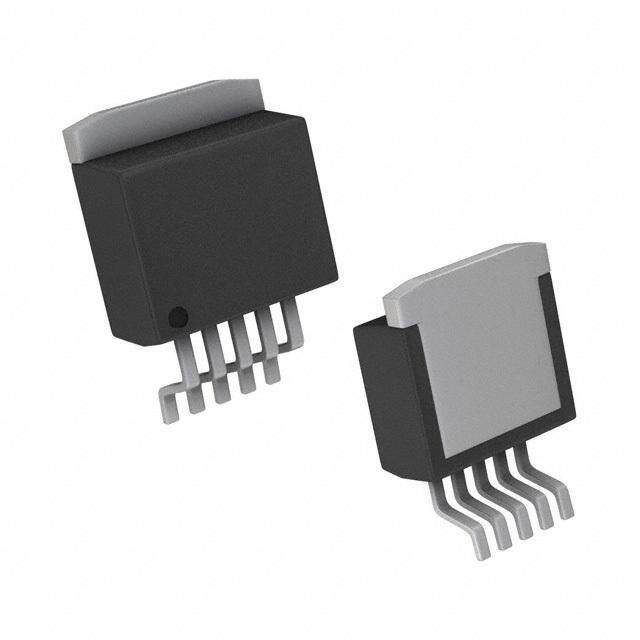
| 产品图片 |
|
| rohs | 符合RoHS无铅 / 符合限制有害物质指令(RoHS)规范要求 |
| 产品系列 | 电源管理 IC,线性稳压器,Texas Instruments TL317CDR- |
| 数据手册 | |
| 产品型号 | TL317CDR |
| PSRR/纹波抑制—典型值 | 80 dB |
| 产品目录页面 | |
| 产品种类 | |
| 供应商器件封装 | 8-SOIC |
| 其它名称 | 296-24385-6 |
| 包装 | Digi-Reel® |
| 单位重量 | 72.600 mg |
| 商标 | Texas Instruments |
| 安装类型 | 表面贴装 |
| 安装风格 | SMD/SMT |
| 封装 | Reel |
| 封装/外壳 | 8-SOIC(0.154",3.90mm 宽) |
| 封装/箱体 | SOIC-8 |
| 工作温度 | 0°C ~ 125°C |
| 工厂包装数量 | 2500 |
| 最大工作温度 | + 125 C |
| 最大输入电压 | 38 V |
| 最小工作温度 | 0 C |
| 最小输入电压 | 5 V |
| 极性 | Positive |
| 标准包装 | 1 |
| 电压-跌落(典型值) | - |
| 电压-输入 | 5 V ~ 38 V |
| 电压-输出 | 1.2 V ~ 32 V |
| 电流-输出 | 100mA |
| 电流-限制(最小值) | - |
| 稳压器拓扑 | 正,可调式 |
| 稳压器数 | 1 |
| 系列 | TL317 |
| 线路调整率 | 0.02 % / V |
| 负载调节 | 0.5 % |
| 输出电压 | 1.2 V to 32 V |
| 输出电流 | 0.1 A |
| 输出端数量 | 1 |
| 输出类型 | Adjustable |


- 商务部:美国ITC正式对集成电路等产品启动337调查
- 曝三星4nm工艺存在良率问题 高通将骁龙8 Gen1或转产台积电
- 太阳诱电将投资9.5亿元在常州建新厂生产MLCC 预计2023年完工
- 英特尔发布欧洲新工厂建设计划 深化IDM 2.0 战略
- 台积电先进制程称霸业界 有大客户加持明年业绩稳了
- 达到5530亿美元!SIA预计今年全球半导体销售额将创下新高
- 英特尔拟将自动驾驶子公司Mobileye上市 估值或超500亿美元
- 三星加码芯片和SET,合并消费电子和移动部门,撤换高东真等 CEO
- 三星电子宣布重大人事变动 还合并消费电子和移动部门
- 海关总署:前11个月进口集成电路产品价值2.52万亿元 增长14.8%


PDF Datasheet 数据手册内容提取
Product Sample & Technical Tools & Support & Folder Buy Documents Software Community TL317 SLVS004I–APRIL1979–REVISEDAUGUST2016 TL317 100-mA 3-Terminal Adjustable Positive Voltage Regulator 1 Features 3 Description • OutputVoltageRangeAdjustableFrom The TL317 is an adjustable three-terminal positive- 1 voltage regulator capable of supplying 100 mA over 1.25Vto32VWhenUsedWithanExternal an output-voltage range of 1.25 V to 32 V. It is ResistorDivider exceptionally easy to use and requires only two • OutputCurrentCapabilityof100mA externalresistorstosettheoutputvoltage. • InputRegulationTypically0.01%Per This regulator offers full overload protection available Input-VoltageChange only in integrated circuits. Included on the chip are • OutputRegulationTypically0.5% current-limiting and thermal-overload protection. All • RippleRejectionTypically80dB overload-protection circuitry remains fully functional, even when ADJUSTMENT is disconnected. Normally, 2 Applications no capacitors are required unless the device is situated far from the input filter capacitors, in which • PowerSupplies case an input bypass is required. An optional output • PortableDevices capacitor can be added to improve transient response. ADJUSTMENT can be bypassed to • ComputingandServers achieveveryhighripplerejection. • Telecommunications In addition to replacing fixed regulators, the TL317 • HVAC:Heating,Ventilation,andAirConditioning regulator is useful in a wide variety of other • DesktopPC applications. Because the regulator is floating and • DigitalSignage sees only the input-to-output differential voltage, supplies of several hundred volts can be regulated as • ProgrammableLogicController longasthemaximuminput-to-outputdifferentialisnot • Appliances exceeded. Its primary application is that of a programmable output regulator, but by connecting a FunctionalBlockDiagram fixed resistor between ADJUSTMENT and OUTPUT, Input this device can be used as a precision current regulator. Supplies with electronic shutdown can be I achieved by clamping ADJUSTMENT to ground, adj programming the output to 1.25 V, where most loads drawlittlecurrent. + DeviceInformation(1) 1.25 V PARTNUMBER PACKAGE BODYSIZE(NOM) OverTemp& TL317D SOIC(8) 4.90mm×3.90mm OverCurrent Protection TL317PW TSSOP(8) 4.30mm×3.00mm Adj. TL317PS SOP(8) 6.20mm×5.30mm TL317LP TO-92(3) 4.83mm×3.68mm (1) For all available packages, see the orderable addendum at theendofthedatasheet. Output Copyright © 2016,Texas Instruments Incorporated 1 An IMPORTANT NOTICE at the end of this data sheet addresses availability, warranty, changes, use in safety-critical applications, intellectualpropertymattersandotherimportantdisclaimers.PRODUCTIONDATA.
TL317 SLVS004I–APRIL1979–REVISEDAUGUST2016 www.ti.com Table of Contents 1 Features.................................................................. 1 7.4 DeviceFunctionalModes.........................................7 2 Applications........................................................... 1 8 ApplicationandImplementation.......................... 8 3 Description............................................................. 1 8.1 ApplicationInformation..............................................8 4 RevisionHistory..................................................... 2 8.2 TypicalApplications..................................................8 5 PinConfigurationandFunctions......................... 3 9 PowerSupplyRecommendations...................... 13 6 Specifications......................................................... 4 10 Layout................................................................... 13 6.1 AbsoluteMaximumRatings......................................4 10.1 LayoutGuidelines.................................................13 6.2 ESDRatings ............................................................4 10.2 LayoutExample....................................................13 6.3 RecommendedOperatingConditions.......................4 11 DeviceandDocumentationSupport................. 14 6.4 ThermalInformation..................................................4 11.1 ReceivingNotificationofDocumentationUpdates14 6.5 ElectricalCharacteristics...........................................5 11.2 CommunityResources..........................................14 6.6 TypicalCharacteristic................................................5 11.3 Trademarks...........................................................14 7 DetailedDescription.............................................. 6 11.4 ElectrostaticDischargeCaution............................14 7.1 Overview ..................................................................6 11.5 Glossary................................................................14 7.2 FunctionalBlockDiagrams.......................................6 12 Mechanical,Packaging,andOrderable Information........................................................... 14 7.3 FeatureDescription..................................................7 4 Revision History NOTE:Pagenumbersforpreviousrevisionsmaydifferfrompagenumbersinthecurrentversion. ChangesfromRevisionH(September2011)toRevisionI Page • AddedESDRatingstable,FeatureDescriptionsection,DeviceFunctionalModes,ApplicationandImplementation section,PowerSupplyRecommendationssection,Layoutsection,DeviceandDocumentationSupportsection,and Mechanical,Packaging,andOrderableInformationsection.................................................................................................. 1 • DeletedOrderingInformationtable,seePOAattheendofthedatasheet............................................................................ 3 ChangesfromRevisionG(September2009)toRevisionH Page • ChangeddatasheetformatfromQuickSilvertoDocZone...................................................................................................... 1 • Changedlowendoutputvoltagerangefrom1.2Vto1.25.................................................................................................... 1 • AddedMINvalueof2.5VforV –V parameterintheRecommendedOperatingConditionstable.................................... 4 I O 2 SubmitDocumentationFeedback Copyright©1979–2016,TexasInstrumentsIncorporated ProductFolderLinks:TL317
TL317 www.ti.com SLVS004I–APRIL1979–REVISEDAUGUST2016 5 Pin Configuration and Functions DPackage 8-PinSOIC PSPackage TopView 8-PinSOP TopView INPUT 1 8 NC INPUT 1 8 OUTPUT OUTPUT 2 7 OUTPUT NC 2 7 NC OUTPUT 3 6 OUTPUT NC 3 6 ADJUSTMENT ADJUSTMENT 4 5 NC NC 4 5 NC Not to scale Not to scale PWPackage 8-PinTSSOP LPPackage TopView 3-PinTO-92 TopView INPUT 1 8 NC NC 2 7 NC NC 3 6 OUTPUT ADJUSTMENT 4 5 NC Not to scale PinFunctions PIN I/O DESCRIPTION NAME SOIC TSSOP SOP TO-92 ADJUSTMENT 4 4 6 3 — Supplyreferencevoltage INPUT 1 1 1 1 I Inputsupplyvoltage NC 5,8 2,3,5,7,8 2,3,4,5,7 — — Nointernalconnection Outputvoltage,outputterminalsareallinternally OUTPUT 2,3,6,7 6 8 2 O connected. Copyright©1979–2016,TexasInstrumentsIncorporated SubmitDocumentationFeedback 3 ProductFolderLinks:TL317
TL317 SLVS004I–APRIL1979–REVISEDAUGUST2016 www.ti.com 6 Specifications 6.1 Absolute Maximum Ratings overoperatingfree-airtemperaturerange(unlessotherwisenoted)(1) MIN MAX UNIT Input-to-outputdifferentialvoltage,V –V 35 V l O Operatingvirtual-junctiontemperature,T 150 °C J Storagetemperaturerange,T –65 150 °C stg (1) StressesbeyondthoselistedunderAbsoluteMaximumRatingsmaycausepermanentdamagetothedevice.Thesearestressratings only,whichdonotimplyfunctionaloperationofthedeviceattheseoranyotherconditionsbeyondthoseindicatedunderRecommended OperatingConditions.Exposuretoabsolute-maximum-ratedconditionsforextendedperiodsmayaffectdevicereliability. 6.2 ESD Ratings VALUE UNIT Human-bodymodel(HBM),perANSI/ESDA/JEDECJS-001(1) ±2000 V Electrostaticdischarge V (ESD) Charged-devicemodel(CDM),perJEDECspecificationJESD22-C101(2) ±1000(3) (1) JEDECdocumentJEP155statesthat500-VHBMallowssafemanufacturingwithastandardESDcontrolprocess. (2) JEDECdocumentJEP157statesthat250-VCDMallowssafemanufacturingwithastandardESDcontrolprocess. (3) TestedonPWpackage. 6.3 Recommended Operating Conditions MIN NOM MAX UNIT V –V Input-to-outputvoltagedifferential 2.5 35 V I O I Outputcurrent 2.5 100 mA O TL317C 0 125 °C T Operatingvirtual-junctiontemperature J TL317 –40 125 °C 6.4 Thermal Information TL317 THERMALMETRIC(1) D(SOIC) PW(TSSOP) PS(SOP) LP(TO-92) UNIT 8PINS 8PINS 8PINS 3PINS R Junction-to-ambientthermalresistance 109.9 170 115.3 157.9 °C/W θJA R Junction-to-case(top)thermalresistance 58.8 51 67.1 81.6 °C/W θJC(top) R Junction-to-boardthermalresistance 58.5 101.5 64.4 — °C/W θJB ψ Junction-to-topcharacterizationparameter 12.5 3.7 27.7 25.4 °C/W JT ψ Junction-to-boardcharacterizationparameter 57.9 99.1 63.5 137.1 °C/W JB (1) Formoreinformationabouttraditionalandnewthermalmetrics,seetheSemiconductorandICPackageThermalMetricsapplication report. 4 SubmitDocumentationFeedback Copyright©1979–2016,TexasInstrumentsIncorporated ProductFolderLinks:TL317
TL317 www.ti.com SLVS004I–APRIL1979–REVISEDAUGUST2016 6.5 Electrical Characteristics overrecommendedoperatingvirtual-junctiontemperaturerange(unlessotherwisenoted)(1) PARAMETER TESTCONDITIONS MIN TYP MAX UNIT T =25°C 0.01% 0.02% Inputvoltageregulation(2) V –V =5Vto35V J V I O I =2.5mAto100mA 0.02% 0.05% O V =10V,f=120Hz 65 O Rippleregulation VO=10V, dB 10-µFcapacitorbetween 66 80 ADJUSTMENTandground V =5Vto35V, V ≤5V 25 mV I O I =2.5mAto100mA, O Outputvoltageregulation TJ=25°C VO≥5V 5 mV/V VI=5Vto35V, VO≤5 50 mV IO=2.5mAto100mA VO≥5V 10 mV/V Outputvoltagechangewithtemperature T =0°Cto125°C 10 mV/V J Outputvoltagelong-termdrift After1000hoursatT =125°CandV –V =35V 3 10 mV/V J I O Outputnoisevoltage f=10Hzto10kHz,T =25°C 30 µV/V J Minimumoutputcurrenttomaintain V –V =35 1.5 2.5 mA regulation I O Peakoutputcurrent V –V ≤35V 100 200 mA I O ADJUSTMENTcurrent 50 100 µA ChangeinADJUSTMENTcurrent V –V =2.5Vto35V,I =2.5mAto100mA 0.2 5 µA I O O Referencevoltage I =2.5mAto100mA,V −V =5Vto35V, O I O 1.2 1.25 1.3 V (outputtoADJUSTMENT) P≤rateddissipation (1) Unlessotherwisenoted,thesespecificationsapplyforthefollowingtestconditions:V –V =5VandI =40mA.Pulse-testing I O O techniquesmustbeusedthatmaintainthejunctiontemperatureasclosetotheambienttemperatureaspossible.Allcharacteristicsare measuredwitha0.1-µFcapacitoracrosstheinputanda1-µFcapacitoracrosstheoutput. (2) Inputvoltageregulationisexpressedhereasthepercentagechangeinoutputvoltageper1-Vchangeattheinput. 6.6 Typical Characteristic 2 1.95 1.9 V) 1.85 e ( g 1.8 a Volt 1.75 out 1.7 p o Dr 1.65 1.6 1.55 1.5 0 10 20 30 40 50 60 70 80 90 100 Load Current (mA) D002 Figure1.DropoutVoltagevsLoadCurrent(T =25°C) J Copyright©1979–2016,TexasInstrumentsIncorporated SubmitDocumentationFeedback 5 ProductFolderLinks:TL317
TL317 SLVS004I–APRIL1979–REVISEDAUGUST2016 www.ti.com 7 Detailed Description 7.1 Overview The TL317 device is an adjustable three-terminal positive-voltage regulator capable of supplying up to 100 mA over an output-voltage range of 1.25 V to 32 V. It requires only two external resistors to set the output voltage. The TL317 device is versatile in its applications, including uses in programmable output regulation and local on- card regulation. Also, by connecting a fixed resistor between the ADJUSTMENT and OUTPUT terminals, the TL317devicecanfunctionasaprecisioncurrentregulator.Anoptionaloutputcapacitorcanbeaddedtoimprove transient response. The ADJUSTMENT terminal can be bypassed to achieve very high ripple-rejection ratios, whicharedifficulttoachievewithstandardthree-terminalregulators. 7.2 Functional Block Diagrams Input I adj + 1.25 V OverTemp& OverCurrent Protection Adj. Output Copyright © 2016,Texas Instruments Incorporated Figure2. EquivalentSchematic INPUT 310Ω 310Ω 190Ω 251Ω 5.6 kΩ 2.1 kΩ 360Ω 200 kΩ 124Ω 11.5kΩ 1.4Ω 30 2.12 kΩ pF 30 195Ω 5.3 kΩ 5.7 kΩ 70Ω 5.1 kΩ pF 10.8 kΩ 670Ω OUTPUT ADJUSTMENT 40Ω Copyright © 2016,Texas Instruments Incorporated Allcomponentvaluesshownarenominal Figure3. DetailedSchematic 6 SubmitDocumentationFeedback Copyright©1979–2016,TexasInstrumentsIncorporated ProductFolderLinks:TL317
TL317 www.ti.com SLVS004I–APRIL1979–REVISEDAUGUST2016 7.3 Feature Description 7.3.1 NPNDarlingtonOutputDrive NPNDarlingtonoutputtopologyprovidesnaturallylowoutputimpedanceandanoutputcapacitorisoptional. 7.3.2 ProgrammableFeedback An internal amplifier with 1.25-V offset input at the ADJUSTMENT terminal provides easy output voltage or current (not both) programming. For current regulation applications, a single resistor whose resistance value is 1.25 V / I and power rating is greater than (1.25 V)2 / R must be used. For voltage regulation applications, two O resistorssettheoutputvoltageasdescribedinAdjustableVoltageRegulator. 7.4 Device Functional Modes 7.4.1 NormalOperation The device OUTPUT pin sources current necessary to make the OUTPUT pin 1.25 V greater than the ADJUSTMENTpintoprovideoutputregulation 7.4.2 OperationWithLowInputVoltage The device requires 2.5 V of headroom (VI – VO) to regulate the OUTPUT. With less headroom, the OUTPUT voltageofthedevicemaybebelowthedesiredsetpoint. 7.4.3 OperationinLightLoads The device passes its bias current to the OUTPUT pin. The load or feedback must consume this minimum current for regulation or the output may be too high. The minimum current require to regulate is provided in the Electrical Characteristics, so the series resistance used to set the output voltage is recommended to be V / I O MIN toensureregulationatalltimes. Copyright©1979–2016,TexasInstrumentsIncorporated SubmitDocumentationFeedback 7 ProductFolderLinks:TL317
TL317 SLVS004I–APRIL1979–REVISEDAUGUST2016 www.ti.com 8 Application and Implementation NOTE Information in the following applications sections is not part of the TI component specification, and TI does not warrant its accuracy or completeness. TI’s customers are responsible for determining suitability of components for their purposes. Customers should validateandtesttheirdesignimplementationtoconfirmsystemfunctionality. 8.1 Application Information The flexibility of the TL317 allows it to be configured to take on many different functions in DC power applications. 8.2 Typical Applications 8.2.1 AdjustableVoltageRegulator TL317 VI Input Output VO(B) Adjustment R1 470Ω C1=0.1mF(A) C2 = 1mF(C) R2 Copyright © 2016,Texas Instruments Incorporated Figure4. AdjustableVoltageRegulator 8.2.1.1 DesignRequirements • R1andR2arerequiredtosettheoutputvoltage. • C1 is recommended, particularly if the regulator is not in close proximity to the power-supply filter capacitors. A 0.1-µF ceramic or 1-µF tantalum capacitor provides sufficient bypassing for most applications, especially whenadjustmentandoutputcapacitorsareused. • Useofanoutputcapacitor,C2,improvestransientresponse,butisoptional. 8.2.1.2 DetailedDesignProcedure V iscalculatedasshowninEquation1.I istypically50 µAandnegligibleinmostapplications. O ADJ Power dissipation for linear regulators is calculated as shown in Equation 2. I is typically 50 µA and negligible ADJ in most applications, so a typical way to calculate power dissipation for linear regulators is simplified to Equation3. V =V (1+R2/R1)+(I ×R2) (1) O REF ADJ P=(V -V )×I +(V -V )×I (2) I O O I ADJ ADJ P=(V -V )×I (3) I O O 8 SubmitDocumentationFeedback Copyright©1979–2016,TexasInstrumentsIncorporated ProductFolderLinks:TL317
TL317 www.ti.com SLVS004I–APRIL1979–REVISEDAUGUST2016 Typical Applications (continued) 8.2.1.3 ApplicationCurve 1.26 1.256 V) (T 1.252 N E M T S DJU 1.248 A V 1.244 1.24 5 10 15 20 25 30 35 VI -VO (V) D001 Figure5.LineRegulation 8.2.2 0-Vto30-VRegulatorCircuit V is calculated as shown in Equation 4, where V equals the difference between OUTPUT and ADJUSTMENT O ref voltages(approximately1.25V). æ R +R ö VOUT= VREFç1+ 2R 3 ÷ -10V è 1 ø (4) TL317 VO(A) 35 V Input Output Adjustment R1 = 120Ω 10 V C1 = 0.1mF R3 = R2 = 3 kΩ 820Ω 1N4002 Copyright © 2016,Texas Instruments Incorporated Figure6. 0-Vto30-VRegulatorCircuitSchematic Copyright©1979–2016,TexasInstrumentsIncorporated SubmitDocumentationFeedback 9 ProductFolderLinks:TL317
TL317 SLVS004I–APRIL1979–REVISEDAUGUST2016 www.ti.com Typical Applications (continued) 8.2.3 RegulatorCircuitWithImprovedRippleRejection • Protection diode D1 is recommended if C2 is used. The diode provides a low-impedance discharge path to preventthecapacitorfromdischargingintotheoutputoftheregulator • Useofanoutputcapacitor,C2,improvestransientresponse,butisoptional. TL317 VI Input Output VO(B) D1(A) Adjustment R1= 1N4002 C1 = 470Ω 0.1mF + R2 = + C3 = 1mF 10 kΩ C2 = 10mF Copyright © 2016,Texas Instruments Incorporated Figure7. RegulatorCircuitWithImprovedRippleRejectionSchematic 8.2.4 PrecisionCurrent-LimiterCircuit TheuseoftheTL317inthisconfigurationlimitstheoutputcurrenttoI showninFigure8. limit TL317 1.25 VI Input Output Ilimit = R1 R1 Adjustment Copyright © 2016,Texas Instruments Incorporated Figure8. PrecisionCurrent-LimiterCircuit 8.2.5 TrackingPreregulatorCircuit ThisapplicationkeepsaconstantvoltageacrossthesecondTL317inthecircuit. R2 = 1.5 kΩ R1 = 470Ω Adjustment VI Input Output TL317 TL317 Input Output VO Adjustment R3= C1 = 0.1mF 240Ω C2 = 1mF R4 = Output 2 kΩ Adjust Copyright © 2016,Texas Instruments Incorporated Figure9. TrackingPreregulatorCircuitSchematic 10 SubmitDocumentationFeedback Copyright©1979–2016,TexasInstrumentsIncorporated ProductFolderLinks:TL317
TL317 www.ti.com SLVS004I–APRIL1979–REVISEDAUGUST2016 Typical Applications (continued) 8.2.6 Slow-Turnon15-VRegulatorCircuit ThecapacitorC1,incombinationwiththePNPtransistor,helpsthecircuittoslowlystartsupplyingvoltage.Inthe beginning, the capacitor is not charged. Therefore, output voltage starts at V + V + 1.25 V = 0 V + 0.65 V + C1 BE 1.25V=1.9V.Asthecapacitorvoltagerises,V alsorisesatthesamerate.Whentheoutputvoltagereaches OUT thevaluedeterminedbyR1andR2,thePNPisturnedoff. TL317 VI Input Output VO= 15 V Adjustment R1= 470Ω 1N4002 R3 = 50 kΩ R2 = 5.1 kΩ 2N2905 C1 = 25mF Copyright © 2016,Texas Instruments Incorporated Figure10. Slow-Turnon15-VRegulatorCircuitSchematic 8.2.7 50-mAConstant-CurrentBattery-ChargerCircuit The current limit operation mode can be used to trickle charge a battery at a fixed current. I = 1.25 V / 24 Ω. CHG V mustbegreaterthanV +4.25V(1.25V[V ]+3V[headroom]). I BAT REF Power dissipation through resistor R1 is calculated as shown in Equation 5, so a resistor with the appropriate powerratingmustbechosenforthisapplication. P(R1)=I 2×R1[Ω] (5) O TL317 24Ω VI Input Output Adjustment Copyright © 2016,Texas Instruments Incorporated Figure11. 50-mAConstant-CurrentBattery-ChargerCircuit Copyright©1979–2016,TexasInstrumentsIncorporated SubmitDocumentationFeedback 11 ProductFolderLinks:TL317
TL317 SLVS004I–APRIL1979–REVISEDAUGUST2016 www.ti.com Typical Applications (continued) 8.2.8 Current-Limited6-VCharger As the charge current increases, the voltage at the bottom resistor increases until the NPN starts sinking current from the adjustment pin. The voltage at the adjustment pin drops, and consequently the output voltage decreasesuntiltheNPNstopsconducting. TL317 VI Input Output Adjustment 240Ω 1.1kΩ ICHG V VBE R I BE CHG V Copyright © 2016,Texas Instruments Incorporated Figure12. Current-Limited6-VChargerSchematic 8.2.9 High-CurrentAdjustableRegulator The NPNs at the top of the schematic allow higher currents at V than the LM317 can provide, while still OUT keepingtheoutputvoltageatlevelsdeterminedbytheadjustmentpinresistordivideroftheLM317. TIP73 2N2905 500Ω VI 5 kΩ TL317 22Ω Input Output VO Adjustment 120Ω 1N4002 10mF RL(A) 47mF 5 kΩ 10mF(B) Copyright © 2016,Texas Instruments Incorporated A. Minimumloadcurrentis30mA. B. Optionalcapacitorimprovesripplesrejection. Figure13. High-CurrentAdjustableRegulatorSchematic 12 SubmitDocumentationFeedback Copyright©1979–2016,TexasInstrumentsIncorporated ProductFolderLinks:TL317
TL317 www.ti.com SLVS004I–APRIL1979–REVISEDAUGUST2016 9 Power Supply Recommendations The TL317 is designed to operate from an input voltage supply range between 1.25 V to 35 V greater than the output voltage. If the device is more than six inches from the input filter capacitors, an input bypass capacitor, 0.1-µF(orgreater),ofanytypeisrequiredforstability. 10 Layout 10.1 Layout Guidelines • Itisrecommendedthattheinputterminalbebypassedtogroundwithabypasscapacitor. • The optimum placement for the bypass capacitor is closest to the input terminal of the device and the system GND.Takecaretominimizetheloopareaformedbythebypass-capacitorconnection,theinputterminal,and thesystemGND. • For operation at full rated load, it is recommended to use wide trace lengths to eliminate I × R drop and heat dissipation. 10.2 Layout Example 0.1 (cid:29)F INPUT 1 8 NC OUTPUT 2 7 OUTPUT OUTPUT 3 6 OUTPUT ADJ 4 5 NC Figure14. TL317DLayoutExample Copyright©1979–2016,TexasInstrumentsIncorporated SubmitDocumentationFeedback 13 ProductFolderLinks:TL317
TL317 SLVS004I–APRIL1979–REVISEDAUGUST2016 www.ti.com 11 Device and Documentation Support 11.1 Receiving Notification of Documentation Updates To receive notification of documentation updates, navigate to the device product folder on ti.com. In the upper right corner, click on Alert me to register and receive a weekly digest of any product information that has changed.Forchangedetails,reviewtherevisionhistoryincludedinanyreviseddocument. 11.2 Community Resources The following links connect to TI community resources. Linked contents are provided "AS IS" by the respective contributors. They do not constitute TI specifications and do not necessarily reflect TI's views; see TI's Terms of Use. TIE2E™OnlineCommunity TI'sEngineer-to-Engineer(E2E)Community.Createdtofostercollaboration amongengineers.Ate2e.ti.com,youcanaskquestions,shareknowledge,exploreideasandhelp solveproblemswithfellowengineers. DesignSupport TI'sDesignSupport QuicklyfindhelpfulE2Eforumsalongwithdesignsupporttoolsand contactinformationfortechnicalsupport. 11.3 Trademarks E2EisatrademarkofTexasInstruments. Allothertrademarksarethepropertyoftheirrespectiveowners. 11.4 Electrostatic Discharge Caution This integrated circuit can be damaged by ESD. Texas Instruments recommends that all integrated circuits be handled with appropriateprecautions.Failuretoobserveproperhandlingandinstallationprocedurescancausedamage. ESDdamagecanrangefromsubtleperformancedegradationtocompletedevicefailure.Precisionintegratedcircuitsmaybemore susceptibletodamagebecauseverysmallparametricchangescouldcausethedevicenottomeetitspublishedspecifications. 11.5 Glossary SLYZ022—TIGlossary. Thisglossarylistsandexplainsterms,acronyms,anddefinitions. 12 Mechanical, Packaging, and Orderable Information The following pages include mechanical, packaging, and orderable information. This information is the most current data available for the designated devices. This data is subject to change without notice and revision of thisdocument.Forbrowser-basedversionsofthisdatasheet,refertotheleft-handnavigation. 14 SubmitDocumentationFeedback Copyright©1979–2016,TexasInstrumentsIncorporated ProductFolderLinks:TL317
PACKAGE OPTION ADDENDUM www.ti.com 6-Feb-2020 PACKAGING INFORMATION Orderable Device Status Package Type Package Pins Package Eco Plan Lead/Ball Finish MSL Peak Temp Op Temp (°C) Device Marking Samples (1) Drawing Qty (2) (6) (3) (4/5) TL317CD ACTIVE SOIC D 8 75 Green (RoHS NIPDAU Level-1-260C-UNLIM 0 to 125 TL317C & no Sb/Br) TL317CDE4 ACTIVE SOIC D 8 75 Green (RoHS NIPDAU Level-1-260C-UNLIM 0 to 125 TL317C & no Sb/Br) TL317CDR ACTIVE SOIC D 8 2500 Green (RoHS NIPDAU | SN Level-1-260C-UNLIM 0 to 125 TL317C & no Sb/Br) TL317CDRE4 ACTIVE SOIC D 8 2500 Green (RoHS NIPDAU Level-1-260C-UNLIM 0 to 125 TL317C & no Sb/Br) TL317CDRG4 ACTIVE SOIC D 8 2500 Green (RoHS NIPDAU Level-1-260C-UNLIM 0 to 125 TL317C & no Sb/Br) TL317CLP ACTIVE TO-92 LP 3 1000 Pb-Free SN N / A for Pkg Type 0 to 125 TL317C (RoHS) TL317CLPE3 ACTIVE TO-92 LP 3 1000 Pb-Free SN N / A for Pkg Type 0 to 125 TL317C (RoHS) TL317CLPR ACTIVE TO-92 LP 3 2000 Pb-Free SN N / A for Pkg Type 0 to 125 TL317C (RoHS) TL317CLPRE3 ACTIVE TO-92 LP 3 2000 Pb-Free SN N / A for Pkg Type 0 to 125 TL317C (RoHS) TL317CPWR ACTIVE TSSOP PW 8 2000 Green (RoHS NIPDAU | SN Level-1-260C-UNLIM 0 to 125 T317 & no Sb/Br) TL317PS ACTIVE SO PS 8 80 Green (RoHS NIPDAU Level-1-260C-UNLIM -40 to 125 T317 & no Sb/Br) TL317PSR ACTIVE SO PS 8 2000 Green (RoHS NIPDAU Level-1-260C-UNLIM -40 to 125 T317 & no Sb/Br) (1) The marketing status values are defined as follows: ACTIVE: Product device recommended for new designs. LIFEBUY: TI has announced that the device will be discontinued, and a lifetime-buy period is in effect. NRND: Not recommended for new designs. Device is in production to support existing customers, but TI does not recommend using this part in a new design. PREVIEW: Device has been announced but is not in production. Samples may or may not be available. OBSOLETE: TI has discontinued the production of the device. (2) RoHS: TI defines "RoHS" to mean semiconductor products that are compliant with the current EU RoHS requirements for all 10 RoHS substances, including the requirement that RoHS substance do not exceed 0.1% by weight in homogeneous materials. Where designed to be soldered at high temperatures, "RoHS" products are suitable for use in specified lead-free processes. TI may reference these types of products as "Pb-Free". RoHS Exempt: TI defines "RoHS Exempt" to mean products that contain lead but are compliant with EU RoHS pursuant to a specific EU RoHS exemption. Addendum-Page 1
PACKAGE OPTION ADDENDUM www.ti.com 6-Feb-2020 Green: TI defines "Green" to mean the content of Chlorine (Cl) and Bromine (Br) based flame retardants meet JS709B low halogen requirements of <=1000ppm threshold. Antimony trioxide based flame retardants must also meet the <=1000ppm threshold requirement. (3) MSL, Peak Temp. - The Moisture Sensitivity Level rating according to the JEDEC industry standard classifications, and peak solder temperature. (4) There may be additional marking, which relates to the logo, the lot trace code information, or the environmental category on the device. (5) Multiple Device Markings will be inside parentheses. Only one Device Marking contained in parentheses and separated by a "~" will appear on a device. If a line is indented then it is a continuation of the previous line and the two combined represent the entire Device Marking for that device. (6) Lead/Ball Finish - Orderable Devices may have multiple material finish options. Finish options are separated by a vertical ruled line. Lead/Ball Finish values may wrap to two lines if the finish value exceeds the maximum column width. Important Information and Disclaimer:The information provided on this page represents TI's knowledge and belief as of the date that it is provided. TI bases its knowledge and belief on information provided by third parties, and makes no representation or warranty as to the accuracy of such information. Efforts are underway to better integrate information from third parties. TI has taken and continues to take reasonable steps to provide representative and accurate information but may not have conducted destructive testing or chemical analysis on incoming materials and chemicals. TI and TI suppliers consider certain information to be proprietary, and thus CAS numbers and other limited information may not be available for release. In no event shall TI's liability arising out of such information exceed the total purchase price of the TI part(s) at issue in this document sold by TI to Customer on an annual basis. Addendum-Page 2
PACKAGE MATERIALS INFORMATION www.ti.com 20-Dec-2018 TAPE AND REEL INFORMATION *Alldimensionsarenominal Device Package Package Pins SPQ Reel Reel A0 B0 K0 P1 W Pin1 Type Drawing Diameter Width (mm) (mm) (mm) (mm) (mm) Quadrant (mm) W1(mm) TL317CDR SOIC D 8 2500 330.0 12.4 6.4 5.2 2.1 8.0 12.0 Q1 TL317CDR SOIC D 8 2500 330.0 12.8 6.4 5.2 2.1 8.0 12.0 Q1 TL317CDRG4 SOIC D 8 2500 330.0 12.4 6.4 5.2 2.1 8.0 12.0 Q1 TL317CPWR TSSOP PW 8 2000 330.0 12.4 7.0 3.6 1.6 8.0 12.0 Q1 PackMaterials-Page1
PACKAGE MATERIALS INFORMATION www.ti.com 20-Dec-2018 *Alldimensionsarenominal Device PackageType PackageDrawing Pins SPQ Length(mm) Width(mm) Height(mm) TL317CDR SOIC D 8 2500 340.5 338.1 20.6 TL317CDR SOIC D 8 2500 364.0 364.0 27.0 TL317CDRG4 SOIC D 8 2500 340.5 338.1 20.6 TL317CPWR TSSOP PW 8 2000 367.0 367.0 35.0 PackMaterials-Page2
PACKAGE OUTLINE D0008A SOIC - 1.75 mm max height SCALE 2.800 SMALL OUTLINE INTEGRATED CIRCUIT C SEATING PLANE .228-.244 TYP [5.80-6.19] .004 [0.1] C A PIN 1 ID AREA 6X .050 [1.27] 8 1 2X .189-.197 [4.81-5.00] .150 NOTE 3 [3.81] 4X (0 -15 ) 4 5 8X .012-.020 B .150-.157 [0.31-0.51] .069 MAX [3.81-3.98] .010 [0.25] C A B [1.75] NOTE 4 .005-.010 TYP [0.13-0.25] 4X (0 -15 ) SEE DETAIL A .010 [0.25] .004-.010 0 - 8 [0.11-0.25] .016-.050 [0.41-1.27] DETAIL A (.041) TYPICAL [1.04] 4214825/C 02/2019 NOTES: 1. Linear dimensions are in inches [millimeters]. Dimensions in parenthesis are for reference only. Controlling dimensions are in inches. Dimensioning and tolerancing per ASME Y14.5M. 2. This drawing is subject to change without notice. 3. This dimension does not include mold flash, protrusions, or gate burrs. Mold flash, protrusions, or gate burrs shall not exceed .006 [0.15] per side. 4. This dimension does not include interlead flash. 5. Reference JEDEC registration MS-012, variation AA. www.ti.com
EXAMPLE BOARD LAYOUT D0008A SOIC - 1.75 mm max height SMALL OUTLINE INTEGRATED CIRCUIT 8X (.061 ) [1.55] SYMM SEE DETAILS 1 8 8X (.024) [0.6] SYMM (R.002 ) TYP [0.05] 5 4 6X (.050 ) [1.27] (.213) [5.4] LAND PATTERN EXAMPLE EXPOSED METAL SHOWN SCALE:8X SOLDER MASK SOLDER MASK METAL OPENING OPENING METAL UNDER SOLDER MASK EXPOSED METAL EXPOSED METAL .0028 MAX .0028 MIN [0.07] [0.07] ALL AROUND ALL AROUND NON SOLDER MASK SOLDER MASK DEFINED DEFINED SOLDER MASK DETAILS 4214825/C 02/2019 NOTES: (continued) 6. Publication IPC-7351 may have alternate designs. 7. Solder mask tolerances between and around signal pads can vary based on board fabrication site. www.ti.com
EXAMPLE STENCIL DESIGN D0008A SOIC - 1.75 mm max height SMALL OUTLINE INTEGRATED CIRCUIT 8X (.061 ) [1.55] SYMM 1 8 8X (.024) [0.6] SYMM (R.002 ) TYP [0.05] 5 4 6X (.050 ) [1.27] (.213) [5.4] SOLDER PASTE EXAMPLE BASED ON .005 INCH [0.125 MM] THICK STENCIL SCALE:8X 4214825/C 02/2019 NOTES: (continued) 8. Laser cutting apertures with trapezoidal walls and rounded corners may offer better paste release. IPC-7525 may have alternate design recommendations. 9. Board assembly site may have different recommendations for stencil design. www.ti.com
None
None
PACKAGE OUTLINE PW0008A TSSOP - 1.2 mm max height SCALE 2.800 SMALL OUTLINE PACKAGE C 6.6 TYP SEATING PLANE 6.2 PIN 1 ID A 0.1 C AREA 6X 0.65 8 1 3.1 2X 2.9 NOTE 3 1.95 4 5 0.30 8X 0.19 4.5 1.2 MAX B 0.1 C A B 4.3 NOTE 4 (0.15) TYP SEE DETAIL A 0.25 GAGE PLANE 0.15 0.75 0 - 8 0.05 0.50 DETAIL A TYPICAL 4221848/A 02/2015 NOTES: 1. All linear dimensions are in millimeters. Any dimensions in parenthesis are for reference only. Dimensioning and tolerancing per ASME Y14.5M. 2. This drawing is subject to change without notice. 3. This dimension does not include mold flash, protrusions, or gate burrs. Mold flash, protrusions, or gate burrs shall not exceed 0.15 mm per side. 4. This dimension does not include interlead flash. Interlead flash shall not exceed 0.25 mm per side. 5. Reference JEDEC registration MO-153, variation AA. www.ti.com
EXAMPLE BOARD LAYOUT PW0008A TSSOP - 1.2 mm max height SMALL OUTLINE PACKAGE 8X (1.5) 8X (0.45) SYMM (R0.05) 1 TYP 8 SYMM 6X (0.65) 5 4 (5.8) LAND PATTERN EXAMPLE SCALE:10X SOOPLEDNEINRG MASK METAL MSOELTDAEL RU NMDAESRK SOOPLEDNEINRG MASK 0.05 MAX 0.05 MIN ALL AROUND ALL AROUND NON SOLDER MASK SOLDER MASK DEFINED DEFINED SOLDER MASK DETAILS NOT TO SCALE 4221848/A 02/2015 NOTES: (continued) 6. Publication IPC-7351 may have alternate designs. 7. Solder mask tolerances between and around signal pads can vary based on board fabrication site. www.ti.com
EXAMPLE STENCIL DESIGN PW0008A TSSOP - 1.2 mm max height SMALL OUTLINE PACKAGE 8X (1.5) SYMM (R0.05) TYP 8X (0.45) 1 8 SYMM 6X (0.65) 5 4 (5.8) SOLDER PASTE EXAMPLE BASED ON 0.125 mm THICK STENCIL SCALE:10X 4221848/A 02/2015 NOTES: (continued) 8. Laser cutting apertures with trapezoidal walls and rounded corners may offer better paste release. IPC-7525 may have alternate design recommendations. 9. Board assembly site may have different recommendations for stencil design. www.ti.com
None
PACKAGE OUTLINE LP0003A TO-92 - 5.34 mm max height SCALE 1.200 SCALE 1.200 TO-92 5.21 4.44 EJECTOR PIN OPTIONAL 5.34 4.32 (1.5) TYP (2.54) SEATING 2X NOTE 3 PLANE 4 MAX (0.51) TYP 6X 0.076 MAX SEATING PLANE 3X 12.7 MIN 0.43 2X 0.55 3X 3X 0.35 2.6 0.2 0.38 2X 1.27 0.13 FORMED LEAD OPTION OTHER DIMENSIONS IDENTICAL STRAIGHT LEAD OPTION TO STRAIGHT LEAD OPTION 2.67 3X 2.03 4.19 3.17 3 2 1 3.43 MIN 4215214/B 04/2017 NOTES: 1. All linear dimensions are in millimeters. Any dimensions in parenthesis are for reference only. Dimensioning and tolerancing per ASME Y14.5M. 2. This drawing is subject to change without notice. 3. Lead dimensions are not controlled within this area. 4. Reference JEDEC TO-226, variation AA. 5. Shipping method: a. Straight lead option available in bulk pack only. b. Formed lead option available in tape and reel or ammo pack. c. Specific products can be offered in limited combinations of shipping medium and lead options. d. Consult product folder for more information on available options. www.ti.com
EXAMPLE BOARD LAYOUT LP0003A TO-92 - 5.34 mm max height TO-92 FULL R TYP 0.05 MAX (1.07) ALL AROUND METAL 3X ( 0.85) HOLE TYP TYP 2X METAL (1.5) 2X (1.5) 2X SOLDER MASK OPENING 1 2 3 (R0.05) TYP 2X (1.07) (1.27) SOLDER MASK (2.54) OPENING LAND PATTERN EXAMPLE STRAIGHT LEAD OPTION NON-SOLDER MASK DEFINED SCALE:15X 0.05 MAX ( 1.4) 2X ( 1.4) ALL AROUND METAL TYP 3X ( 0.9) HOLE METAL 2X (R0.05) TYP 1 2 3 SOLDER MASK OPENING (2.6) SOLDER MASK OPENING (5.2) LAND PATTERN EXAMPLE FORMED LEAD OPTION NON-SOLDER MASK DEFINED SCALE:15X 4215214/B 04/2017 www.ti.com
TAPE SPECIFICATIONS LP0003A TO-92 - 5.34 mm max height TO-92 13.7 11.7 32 23 (2.5) TYP 0.5 MIN 16.5 15.5 11.0 9.75 8.5 8.50 19.0 17.5 2.9 6.75 3.7-4.3 TYP TYP 2.4 5.95 13.0 12.4 FOR FORMED LEAD OPTION PACKAGE 4215214/B 04/2017 www.ti.com
IMPORTANTNOTICEANDDISCLAIMER TI PROVIDES TECHNICAL AND RELIABILITY DATA (INCLUDING DATASHEETS), DESIGN RESOURCES (INCLUDING REFERENCE DESIGNS), APPLICATION OR OTHER DESIGN ADVICE, WEB TOOLS, SAFETY INFORMATION, AND OTHER RESOURCES “AS IS” AND WITH ALL FAULTS, AND DISCLAIMS ALL WARRANTIES, EXPRESS AND IMPLIED, INCLUDING WITHOUT LIMITATION ANY IMPLIED WARRANTIES OF MERCHANTABILITY, FITNESS FOR A PARTICULAR PURPOSE OR NON-INFRINGEMENT OF THIRD PARTY INTELLECTUAL PROPERTY RIGHTS. These resources are intended for skilled developers designing with TI products. You are solely responsible for (1) selecting the appropriate TI products for your application, (2) designing, validating and testing your application, and (3) ensuring your application meets applicable standards, and any other safety, security, or other requirements. These resources are subject to change without notice. TI grants you permission to use these resources only for development of an application that uses the TI products described in the resource. Other reproduction and display of these resources is prohibited. No license is granted to any other TI intellectual property right or to any third party intellectual property right. TI disclaims responsibility for, and you will fully indemnify TI and its representatives against, any claims, damages, costs, losses, and liabilities arising out of your use of these resources. TI’s products are provided subject to TI’s Terms of Sale (www.ti.com/legal/termsofsale.html) or other applicable terms available either on ti.com or provided in conjunction with such TI products. TI’s provision of these resources does not expand or otherwise alter TI’s applicable warranties or warranty disclaimers for TI products. Mailing Address: Texas Instruments, Post Office Box 655303, Dallas, Texas 75265 Copyright © 2020, Texas Instruments Incorporated