ICGOO在线商城 > 集成电路(IC) > PMIC - 稳压器 - 线性 > LD1117DT50TR

 Datasheet下载
- 型号: LD1117DT50TR
- 制造商: STMicroelectronics
- 库位|库存: xxxx|xxxx
- 要求:
| 数量阶梯 | 香港交货 | 国内含税 |
| +xxxx | $xxxx | ¥xxxx |
查看当月历史价格
查看今年历史价格
LD1117DT50TR产品简介:
ICGOO电子元器件商城为您提供LD1117DT50TR由STMicroelectronics设计生产,在icgoo商城现货销售,并且可以通过原厂、代理商等渠道进行代购。 LD1117DT50TR价格参考¥0.87-¥1.15。STMicroelectronicsLD1117DT50TR封装/规格:PMIC - 稳压器 - 线性, Linear Voltage Regulator IC Positive Fixed 1 Output 5V 800mA DPAK。您可以下载LD1117DT50TR参考资料、Datasheet数据手册功能说明书,资料中有LD1117DT50TR 详细功能的应用电路图电压和使用方法及教程。
STMicroelectronics的LD1117DT50TR是一款线性稳压器,属于PMIC(电源管理集成电路)系列。它具有低 dropout(低压差)特性,能够在输入电压与输出电压之间的压差较小的情况下稳定工作。这款稳压器的主要应用场景包括:

1. 便携式设备:由于其低功耗和小封装尺寸,LD1117DT50TR非常适合用于便携式电子设备,如智能手机、平板电脑、可穿戴设备等。这些设备通常需要高效的电源管理以延长电池寿命。

2. 嵌入式系统:在各种嵌入式系统中,如工业控制器、传感器模块和物联网(IoT)设备,LD1117DT50TR可以提供稳定的电源输出,确保系统的可靠性和性能。

3. 消费电子产品:该稳压器适用于多种消费电子产品,如音频设备、智能家居设备、手持游戏机等。它的简单设计和易于集成的特点使其成为许多产品的首选。

4. 通信设备:在通信领域,如路由器、调制解调器和其他网络设备中,LD1117DT50TR能够为关键组件提供稳定的电源,确保数据传输的可靠性和稳定性。

5. 医疗设备:对于一些对电源稳定性要求极高的医疗设备,如便携式医疗仪器、心率监测器等,LD1117DT50TR的高精度和低噪声特性非常适用,能够保证设备的准确性和安全性。

6. 汽车电子:在汽车行业中,LD1117DT50TR可用于车载信息娱乐系统、传感器模块和其他辅助驾驶系统。其宽工作温度范围和抗电磁干扰能力使其适合严苛的汽车环境。

总之,LD1117DT50TR凭借其高效、稳定和易于使用的特性,广泛应用于各种需要可靠电源管理的场合,特别是在那些对尺寸、功耗和稳定性有严格要求的应用中表现出色。
| 参数 | 数值 |
| 产品目录 | 集成电路 (IC)半导体 |
| 描述 | IC REG LDO 5V 0.8A DPAK低压差稳压器 5.0V 0.8A Positive |
| 产品分类 | |
| 品牌 | STMicroelectronics |
| 产品手册 | |
| 产品图片 |
|
| rohs | 符合RoHS无铅 / 符合限制有害物质指令(RoHS)规范要求 |
| 产品系列 | 电源管理 IC,低压差稳压器,STMicroelectronics LD1117DT50TR- |
| 数据手册 | |
| 产品型号 | LD1117DT50TR |
| 产品目录页面 | |
| 产品种类 | 低压差稳压器 |
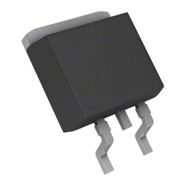
| 供应商器件封装 | D-Pak |
| 其它名称 | 497-1238-1 |
| 其它有关文件 | http://www.st.com/web/catalog/sense_power/FM142/CL1015/SC312/PF63479?referrer=70071840 |
| 包装 | 剪切带 (CT) |
| 商标 | STMicroelectronics |
| 回动电压—最大值 | 1.1 V |
| 安装类型 | 表面贴装 |
| 安装风格 | SMD/SMT |
| 封装 | Reel |
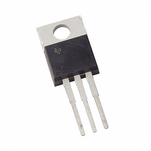
| 封装/外壳 | TO-252-3,DPak(2 引线+接片),SC-63 |
| 封装/箱体 | TO-252 |
| 工作温度 | 0°C ~ 125°C |
| 工厂包装数量 | 2500 |
| 最大功率耗散 | 12 W |
| 最大工作温度 | + 150 C |
| 最大输入电压 | 15 V |
| 最小工作温度 | 0 C |
| 标准包装 | 1 |
| 电压-跌落(典型值) | 1.1V @ 800mA |
| 电压-输入 | 最高 15V |
| 电压-输出 | 5V |
| 电压调节准确度 | 1 % |
| 电流-输出 | 800mA |
| 电流-限制(最小值) | - |
| 稳压器拓扑 | 正,固定式 |
| 稳压器数 | 1 |
| 系列 | LD1117DT5 |
| 线路调整率 | 10 mV |
| 负载调节 | 15 mV |
| 输入偏压电流—最大 | 5 mA |
| 输出电压 | 5 V |
| 输出电流 | 950 mA |
| 输出端数量 | 1 Output |
| 输出类型 | Fixed |


- 商务部:美国ITC正式对集成电路等产品启动337调查
- 曝三星4nm工艺存在良率问题 高通将骁龙8 Gen1或转产台积电
- 太阳诱电将投资9.5亿元在常州建新厂生产MLCC 预计2023年完工
- 英特尔发布欧洲新工厂建设计划 深化IDM 2.0 战略
- 台积电先进制程称霸业界 有大客户加持明年业绩稳了
- 达到5530亿美元!SIA预计今年全球半导体销售额将创下新高
- 英特尔拟将自动驾驶子公司Mobileye上市 估值或超500亿美元
- 三星加码芯片和SET,合并消费电子和移动部门,撤换高东真等 CEO
- 三星电子宣布重大人事变动 还合并消费电子和移动部门
- 海关总署:前11个月进口集成电路产品价值2.52万亿元 增长14.8%


PDF Datasheet 数据手册内容提取
LD1117 Adjustable and fixed low drop positive voltage regulator Datasheet - production data Description The LD1117 is a low drop voltage regulator able to provide up to 800 mA of output current, available even in adjustable version DPAK (V =1.25V). Concerning fixed versions, are REF offered the following output voltages: 1.2 V, 1.8 V, TO-220 2.5 V, 2.85 V, 3.3 V and 5.0 V. The device is supplied in: SOT-223, DPAK, SO-8 and TO-220. The SOT-223 and DPAK surface mount packages optimize the thermal characteristics even offering SOT-223 SO-8 a relevant space saving effect. High efficiency is assured by NPN pass transistor. In fact in this case, unlike than PNP one, the quiescent current Features flows mostly into the load. Only a very common 10 µF minimum capacitor is needed for stability. • Low dropout voltage (1 V typ.) On chip trimming allows the regulator to reach a • 2.85 V device performances are suitable for very tight output voltage tolerance, within ± 1 % at SCSI-2 active termination 25 °C. The adjustable LD1117 is pin to pin • Output current up to 800 mA compatible with the other standard. Adjustable voltage regulators maintaining the better • Fixed output voltage of: 1.2 V, 1.8 V, 2.5 V, performances in terms of drop and tolerance. 3.3V, 5.0 V • Adjustable version availability (V = 1.25 V) REF • Internal current and thermal limit • Available in ± 1 % (at 25 °C) and 2 % in full temperature range • Supply voltage rejection: 75 dB (typ.) February 2020 DocID2572 Rev 37 1/46 This is information on a product in full production. www.st.com 46
Contents LD1117 Contents 1 Diagram . . . . . . . . . . . . . . . . . . . . . . . . . . . . . . . . . . . . . . . . . . . . . . . . . . . 5 2 Pin configuration . . . . . . . . . . . . . . . . . . . . . . . . . . . . . . . . . . . . . . . . . . . 6 3 Maximum ratings . . . . . . . . . . . . . . . . . . . . . . . . . . . . . . . . . . . . . . . . . . . . 7 4 Schematic application . . . . . . . . . . . . . . . . . . . . . . . . . . . . . . . . . . . . . . . 8 5 Electrical characteristics . . . . . . . . . . . . . . . . . . . . . . . . . . . . . . . . . . . . . 9 6 Typical application . . . . . . . . . . . . . . . . . . . . . . . . . . . . . . . . . . . . . . . . . 21 7 LD1117 adjustable: application note . . . . . . . . . . . . . . . . . . . . . . . . . . . 24 8 Package information . . . . . . . . . . . . . . . . . . . . . . . . . . . . . . . . . . . . . . . . 25 9 Packaging mechanical data . . . . . . . . . . . . . . . . . . . . . . . . . . . . . . . . . . 38 10 Order codes . . . . . . . . . . . . . . . . . . . . . . . . . . . . . . . . . . . . . . . . . . . . . . . 44 11 Revision history . . . . . . . . . . . . . . . . . . . . . . . . . . . . . . . . . . . . . . . . . . . 45 2/46 DocID2572 Rev 37
LD1117 List of tables List of tables Table 1. Absolute maximum ratings. . . . . . . . . . . . . . . . . . . . . . . . . . . . . . . . . . . . . . . . . . . . . . . . . . 7 Table 2. Thermal data. . . . . . . . . . . . . . . . . . . . . . . . . . . . . . . . . . . . . . . . . . . . . . . . . . . . . . . . . . . . . 7 Table 3. Electrical characteristics of LD1117#12 . . . . . . . . . . . . . . . . . . . . . . . . . . . . . . . . . . . . . . . . 9 Table 4. Electrical characteristics of LD1117#18 . . . . . . . . . . . . . . . . . . . . . . . . . . . . . . . . . . . . . . . 10 Table 5. Electrical characteristics of LD1117#25 . . . . . . . . . . . . . . . . . . . . . . . . . . . . . . . . . . . . . . . 11 Table 6. Electrical characteristics of LD1117#33 . . . . . . . . . . . . . . . . . . . . . . . . . . . . . . . . . . . . . . . 12 Table 7. Electrical characteristics of LD1117#50 . . . . . . . . . . . . . . . . . . . . . . . . . . . . . . . . . . . . . . . 13 Table 8. Electrical characteristics of LD1117 (adjustable) . . . . . . . . . . . . . . . . . . . . . . . . . . . . . . . . 14 Table 9. Electrical characteristics of LD1117#12C. . . . . . . . . . . . . . . . . . . . . . . . . . . . . . . . . . . . . . 15 Table 10. Electrical characteristics of LD1117#18C. . . . . . . . . . . . . . . . . . . . . . . . . . . . . . . . . . . . . . 16 Table 11. Electrical characteristics of LD1117#25C. . . . . . . . . . . . . . . . . . . . . . . . . . . . . . . . . . . . . . 17 Table 12. Electrical characteristics of LD1117#33C. . . . . . . . . . . . . . . . . . . . . . . . . . . . . . . . . . . . . . 18 Table 13. Electrical characteristics of LD1117#50C. . . . . . . . . . . . . . . . . . . . . . . . . . . . . . . . . . . . . . 19 Table 14. Electrical characteristics of LD1117C (adjustable). . . . . . . . . . . . . . . . . . . . . . . . . . . . . . . 20 Table 15. TO-220 mechanical data (type STD-ST Dual Gauge) . . . . . . . . . . . . . . . . . . . . . . . . . . . . 25 Table 16. TO-220 mechanical data (type STD-ST Single Gauge) . . . . . . . . . . . . . . . . . . . . . . . . . . . 27 Table 17. SOT-223 mechanical data . . . . . . . . . . . . . . . . . . . . . . . . . . . . . . . . . . . . . . . . . . . . . . . . . 29 Table 18. SO-8 mechanical data . . . . . . . . . . . . . . . . . . . . . . . . . . . . . . . . . . . . . . . . . . . . . . . . . . . . 30 Table 19. DPAK (TO-252) mechanical data (type A) . . . . . . . . . . . . . . . . . . . . . . . . . . . . . . . . . . . . . 31 Table 20. DPAK (TO-252) mechanical data (type E) . . . . . . . . . . . . . . . . . . . . . . . . . . . . . . . . . . . . . 33 Table 21. DPAK (TO-252) mechanical data type I. . . . . . . . . . . . . . . . . . . . . . . . . . . . . . . . . . . . . . . 35 Table 22. Footprint data . . . . . . . . . . . . . . . . . . . . . . . . . . . . . . . . . . . . . . . . . . . . . . . . . . . . . . . . . . . 37 Table 23. SOT-223 tape and reel mechanical data . . . . . . . . . . . . . . . . . . . . . . . . . . . . . . . . . . . . . . 39 Table 24. SO-8 tape and reel mechanical data . . . . . . . . . . . . . . . . . . . . . . . . . . . . . . . . . . . . . . . . . 41 Table 25. DPAK tape and reel mechanical data. . . . . . . . . . . . . . . . . . . . . . . . . . . . . . . . . . . . . . . . . 42 Table 26. Order codes . . . . . . . . . . . . . . . . . . . . . . . . . . . . . . . . . . . . . . . . . . . . . . . . . . . . . . . . . . . . 44 Table 27. Document revision history . . . . . . . . . . . . . . . . . . . . . . . . . . . . . . . . . . . . . . . . . . . . . . . . . 45 DocID2572 Rev 37 3/46
List of figures LD1117 List of figures Figure 1. Block diagram. . . . . . . . . . . . . . . . . . . . . . . . . . . . . . . . . . . . . . . . . . . . . . . . . . . . . . . . . . . . 5 Figure 2. Pin connections (top view) . . . . . . . . . . . . . . . . . . . . . . . . . . . . . . . . . . . . . . . . . . . . . . . . . . 6 Figure 3. Application circuit (for 1.2 V). . . . . . . . . . . . . . . . . . . . . . . . . . . . . . . . . . . . . . . . . . . . . . . . . 8 Figure 4. Application circuit (for other fixed output voltages). . . . . . . . . . . . . . . . . . . . . . . . . . . . . . . . 8 Figure 5. Negative supply . . . . . . . . . . . . . . . . . . . . . . . . . . . . . . . . . . . . . . . . . . . . . . . . . . . . . . . . . 21 Figure 6. Circuit for increasing output voltage. . . . . . . . . . . . . . . . . . . . . . . . . . . . . . . . . . . . . . . . . . 21 Figure 7. Voltage regulator with reference. . . . . . . . . . . . . . . . . . . . . . . . . . . . . . . . . . . . . . . . . . . . . 21 Figure 8. Battery backed-up regulated supply. . . . . . . . . . . . . . . . . . . . . . . . . . . . . . . . . . . . . . . . . . 22 Figure 9. Post-regulated dual supply. . . . . . . . . . . . . . . . . . . . . . . . . . . . . . . . . . . . . . . . . . . . . . . . . 23 Figure 10. Adjustable output voltage application. . . . . . . . . . . . . . . . . . . . . . . . . . . . . . . . . . . . . . . . . 24 Figure 11. Adjustable output voltage application with improved ripple rejection . . . . . . . . . . . . . . . . . 24 Figure 12. Drawing dimension TO-220 (type STD-ST Dual Gauge) . . . . . . . . . . . . . . . . . . . . . . . . . . 26 Figure 13. Drawing dimension TO-220 (type STD-ST Single Gauge). . . . . . . . . . . . . . . . . . . . . . . . . 28 Figure 14. Drawing dimension SOT-223 . . . . . . . . . . . . . . . . . . . . . . . . . . . . . . . . . . . . . . . . . . . . . . . 29 Figure 15. Drawing dimension SO-8 . . . . . . . . . . . . . . . . . . . . . . . . . . . . . . . . . . . . . . . . . . . . . . . . . . 30 Figure 16. DPAK (TO-252) package outline A. . . . . . . . . . . . . . . . . . . . . . . . . . . . . . . . . . . . . . . . . . . 32 Figure 17. DPAK (TO-252) package outline E. . . . . . . . . . . . . . . . . . . . . . . . . . . . . . . . . . . . . . . . . . . 34 Figure 18. DPAK (TO-252) package outline I . . . . . . . . . . . . . . . . . . . . . . . . . . . . . . . . . . . . . . . . . . . 36 Figure 19. DPAK footprint recommended data . . . . . . . . . . . . . . . . . . . . . . . . . . . . . . . . . . . . . . . . . . 37 Figure 20. Drawing dimension tube for TO-220 Dual Gauge (mm.) . . . . . . . . . . . . . . . . . . . . . . . . . . 38 Figure 21. Drawing dimension tube for TO-220 Single Gauge (mm.) . . . . . . . . . . . . . . . . . . . . . . . . . 38 Figure 22. Tape for SOT-223 (dimensions are in mm) . . . . . . . . . . . . . . . . . . . . . . . . . . . . . . . . . . . . 39 Figure 23. Reel for SOT-223 (dimensions are in mm). . . . . . . . . . . . . . . . . . . . . . . . . . . . . . . . . . . . . 40 Figure 24. SO-8 tape and reel dimensions . . . . . . . . . . . . . . . . . . . . . . . . . . . . . . . . . . . . . . . . . . . . . 41 Figure 25. Tape for DPAK . . . . . . . . . . . . . . . . . . . . . . . . . . . . . . . . . . . . . . . . . . . . . . . . . . . . . . . . . . 43 Figure 26. Reel for DPAK . . . . . . . . . . . . . . . . . . . . . . . . . . . . . . . . . . . . . . . . . . . . . . . . . . . . . . . . . . 43 4/46 DocID2572 Rev 37
LD1117 Diagram 1 Diagram Figure 1. Block diagram DocID2572 Rev 37 5/46
Pin configuration LD1117 2 Pin configuration Figure 2. Pin connections (top view) (cid:36)(cid:39)(cid:45)(cid:18)(cid:42)(cid:49)(cid:39) (cid:20) (cid:27) (cid:49)(cid:38) (cid:57) (cid:57) (cid:50)(cid:56)(cid:55) (cid:50)(cid:56)(cid:55) (cid:20) (cid:21) (cid:22) (cid:57)(cid:50)(cid:56)(cid:55) (cid:57)(cid:50)(cid:56)(cid:55) (cid:57)(cid:44)(cid:49) (cid:23) (cid:24) (cid:49)(cid:38) (cid:36)(cid:39)(cid:45)(cid:18)(cid:42)(cid:49)(cid:39) (cid:57)(cid:50)(cid:56)(cid:55) (cid:57)(cid:44)(cid:49) SOT-223 SO-8 (cid:22) (cid:57)(cid:44)(cid:49) (cid:22) (cid:57)(cid:44)(cid:49) (cid:21) (cid:57)(cid:50)(cid:56)(cid:55) (cid:21) (cid:57)(cid:50)(cid:56)(cid:55) (cid:20) (cid:36)(cid:39)(cid:45)(cid:18)(cid:42)(cid:49)(cid:39) (cid:20) (cid:36)(cid:39)(cid:45)(cid:18)(cid:42)(cid:49)(cid:39) DPAK TO-220 Note: The TAB is connected to the V . OUT 6/46 DocID2572 Rev 37
LD1117 Maximum ratings 3 Maximum ratings Table 1. Absolute maximum ratings Symbol Parameter Value Unit V (1) DC input voltage 15 V IN P Power dissipation 12 W TOT T Storage temperature range -40 to +150 °C STG for C version -40 to +125 °C T Operating junction temperature range OP for standard version 0 to +125 °C 1. Absolute maximum rating of V = 18 V, when I is lower than 20 mA. IN OUT Table 2. Thermal data Symbol Parameter SOT-223 SO-8 DPAK TO-220 Unit R Thermal resistance junction-case 15 20 8 5 °C/W thJC R Thermal resistance junction-ambient 110 55 100 50 °C/W thJA DocID2572 Rev 37 7/46
Schematic application LD1117 4 Schematic application Figure 3. Application circuit (for 1.2 V) Figure 4. Application circuit (for other fixed output voltages) 8/46 DocID2572 Rev 37
LD1117 Electrical characteristics 5 Electrical characteristics Refer to the test circuits, T = 0 to 125 °C, C = 10 µF, R = 120 W between GND and OUT J O pins, unless otherwise specified. Table 3. Electrical characteristics of LD1117#12 Symbol Parameter Test condition Min. Typ. Max. Unit V Output voltage V = 3.2 V, I = 10 mA, T = 25 °C 1.188 1.20 1.212 V O in O J I = 10 to 800 mA V Output voltage O 1.140 1.20 1.260 V O V - V = 1.4 to 10 V in O D V Line regulation V - V = 1.5 to 13.75 V, I = 10 mA 0.035 0.2 % O in O O D V Load regulation V - V = 3 V, I = 10 to 800 mA 0.1 0.4 % O in O O D V Temperature stability 0.5 % O D V Long term stability 1000 hrs, T = 125 °C 0.3 % O J V Operating input voltage 15 V in I Adjustment pin current V £ 15 V 60 120 µA adj in V - V = 1.4 to 10 V D I Adjustment pin current change in O 1 5 µA adj I = 10 to 800 mA O I Minimum load current V = 15 V 2 5 mA O(min) in I Output current V - V = 5 V, T = 25 °C 800 950 1300 mA O in O J eN Output noise (%V ) B = 10 Hz to 10 kHz, T = 25 °C 0.003 % O J I = 40 mA, f = 120 Hz, T = 25 °C SVR Supply voltage rejection O J 60 75 dB V - V = 3 V, V = 1 V in O ripple PP I = 100 mA 1 1.1 O V Dropout voltage I = 500 mA 1.05 1.15 V d O I = 800 mA 1.10 1.2 O Thermal regulation T = 25 °C, 30 ms Pulse 0.01 0.1 %/W a DocID2572 Rev 37 9/46
Electrical characteristics LD1117 Refer to the test circuits, T = 0 to 125 °C, C = 10 µF, unless otherwise specified. J O Table 4. Electrical characteristics of LD1117#18 Symbol Parameter Test condition Min. Typ. Max. Unit V Output voltage V = 3.8 V, I = 10 mA, T = 25 °C 1.78 1.8 1.82 V O in O J V Output voltage I = 0 to 800 mA, V = 3.3 to 8 V 1.76 1.84 V O O in D V Line regulation V = 3.3 to 8 V, I = 0 mA 1 6 mV O in O D V Load regulation V = 3.3 V, I = 0 to 800 mA 1 10 mV O in O D V Temperature stability 0.5 % O D V Long term stability 1000 hrs, T = 125 °C 0.3 % O J V Operating input voltage I = 100 mA 15 V in O I Quiescent current V £ 8 V 5 10 mA d in I Output current V = 6.8 V, T = 25 °C 800 950 1300 mA O in J eN Output noise voltage B = 10 Hz to 10 kHz, T = 25 °C 100 µV J I = 40 mA, f = 120 Hz, T = 25 °C SVR Supply voltage rejection O J 60 75 dB V = 5.5 V, V = 1 V in ripple PP I = 100 mA 1 1.1 O V Dropout voltage I = 500 mA 1.05 1.15 V d O I = 800 mA 1.10 1.2 O Thermal regulation T = 25 °C, 30 ms Pulse 0.01 0.1 %/W a 10/46 DocID2572 Rev 37
LD1117 Electrical characteristics Refer to the test circuits, T = 0 to 125 °C, C = 10 µF, unless otherwise specified. J O Table 5. Electrical characteristics of LD1117#25 Symbol Parameter Test condition Min. Typ. Max. Unit V Output voltage V = 4.5 V, I = 10 mA, T = 25 °C 2.475 2.5 2.525 V O in O J V Output voltage I = 0 to 800 mA, V = 3.9 to 10 V 2.45 2.55 V O O in D V Line regulation V = 3.9 to 10 V, I = 0 mA 1 6 mV O in O D V Load regulation V = 3.9 V, I = 0 to 800 mA 1 10 mV O in O D V Temperature stability 0.5 % O D V Long term stability 1000 hrs, T = 125 °C 0.3 % O J V Operating input voltage I = 100 mA 15 V in O I Quiescent current V £ 10 V 5 10 mA d in I Output current V = 7.5 V T = 25 °C 800 950 1300 mA O in J eN Output noise voltage B = 10 Hz to 10 kHz, T = 25 °C 100 µV J I = 40 mA, f = 120 Hz, T = 25 °C SVR Supply voltage rejection O J 60 75 dB V = 5.5 V, V = 1 V in ripple PP I = 100 mA 1 1.1 O V Dropout voltage I = 500 mA 1.05 1.15 V d O I = 800 mA 1.10 1.2 O Thermal regulation T = 25 °C, 30 ms Pulse 0.01 0.1 %/W a DocID2572 Rev 37 11/46
Electrical characteristics LD1117 Refer to the test circuits, T = 0 to 125 °C, C = 10 µF, unless otherwise specified. J O Table 6. Electrical characteristics of LD1117#33 Symbol Parameter Test condition Min. Typ. Max. Unit V Output voltage V = 5.3 V, I = 10 mA, T = 25 °C 3.267 3.3 3.333 V O in O J V Output voltage I = 0 to 800 mA, V = 4.75 to 10 V 3.235 3.365 V O O in D V Line regulation V = 4.75 to 15 V, I = 0 mA 1 6 mV O in O D V Load regulation V = 4.75 V, I = 0 to 800 mA 1 10 mV O in O D V Temperature stability 0.5 % O D V Long term stability 1000 hrs, T = 125 °C 0.3 % O J V Operating input voltage I = 100 mA 15 V in O I Quiescent current V £ 15 V 5 10 mA d in I Output current V = 8.3 V, T = 25 °C 800 950 1300 mA O in J eN Output noise voltage B = 10 Hz to 10 kHz, T = 25 °C 100 µV J I = 40 mA, f = 120 Hz, T = 25 °C SVR Supply voltage rejection O J 60 75 dB V = 6.3 V, V = 1 V in ripple PP I = 100 mA 1 1.1 O V Dropout voltage I = 500 mA 1.05 1.15 V d O I = 800 mA 1.10 1.2 O Thermal regulation T = 25 °C, 30 ms Pulse 0.01 0.1 %/W a 12/46 DocID2572 Rev 37
LD1117 Electrical characteristics Refer to the test circuits, T = 0 to 125 °C, C = 10 µF, unless otherwise specified. J O Table 7. Electrical characteristics of LD1117#50 Symbol Parameter Test condition Min. Typ. Max. Unit V Output voltage V = 7 V, I = 10 mA, T = 25 °C 4.95 5 5.05 V O in O J V Output voltage I = 0 to 800 mA, V = 6.5 to 15 V 4.9 5.1 V O O in D V Line regulation V = 6.5 to 15 V, I = 0 mA 1 10 mV O in O D V Load regulation V = 6.5 V, I = 0 to 800 mA 1 15 mV O in O D V Temperature stability 0.5 % O D V Long term stability 1000 hrs, T = 125 °C 0.3 % O J V Operating input voltage I = 100 mA 15 V in O I Quiescent current V £ 15 V 5 10 mA d in I Output current V = 10 V, T = 25 °C 800 950 1300 mA O in J eN Output noise voltage B = 10 Hz to 10 kHz, T = 25 °C 100 µV J I = 40 mA, f = 120 Hz, T = 25 °C SVR Supply voltage rejection O J 60 75 dB V = 8 V, V = 1 V in ripple PP I = 100 mA 1 1.1 O V Dropout voltage I = 500 mA 1.05 1.15 V d O I = 800 mA 1.10 1.2 O Thermal regulation T = 25 °C, 30 ms Pulse 0.01 0.1 %/W a DocID2572 Rev 37 13/46
Electrical characteristics LD1117 Refer to the test circuits, T = 0 to 125 °C, C = 10 µF, unless otherwise specified. J O Table 8. Electrical characteristics of LD1117 (adjustable) Symbol Parameter Test condition Min. Typ. Max. Unit V Reference voltage V - V = 2 V, I = 10 mA, T = 25 °C 1.238 1.25 1.262 V ref in O O J V Reference voltage I = 10 to 800 mA, V - V = 1.4 to 10 V 1.225 1.275 V ref O in O D V Line regulation V - V = 1.5 to 13.75 V, I = 10 mA 0.035 0.2 % O in O O D V Load regulation V - V = 3 V, I = 10 to 800 mA 0.1 0.4 % O in O O D V Temperature stability 0.5 % O D V Long term stability 1000 hrs, T = 125 °C 0.3 % O J V Operating input voltage 15 V in I Adjustment pin current V £ 15 V 60 120 µA adj in D I Adjustment pin current change V - V = 1.4 to 10 V, I = 10 to 800 mA 1 5 µA adj in O O I Minimum load current V = 15 V 2 5 mA O(min) in I Output current V - V = 5 V, T = 25 °C 800 950 1300 mA O in O J eN Output noise (%V ) B = 10 Hz to 10 kHz, T = 25 °C 0.003 % O J I = 40 mA, f = 120 Hz, T = 25 °C SVR Supply voltage rejection O J 60 75 dB V - V = 3 V, V = 1 V in O ripple PP I = 100 mA 1 1.1 O V Dropout voltage I = 500 mA 1.05 1.15 V d O I = 800 mA 1.10 1.2 O Thermal regulation T = 25 °C, 30 ms Pulse 0.01 0.1 %/W a 14/46 DocID2572 Rev 37
LD1117 Electrical characteristics Refer to the test circuits, T = -40 to 125 °C, C = 10 µF, R = 120 W between GND and OUT J O pins, unless otherwise specified. Table 9. Electrical characteristics of LD1117#12C Symbol Parameter Test condition Min. Typ. Max. Unit V Output voltage V - V = 2 V, I = 10 mA, T = 25 °C 1.176 1.20 1.224 V O in O O J V Output voltage I = 10 to 800 mA, V - V = 1.4 to 10 V 1.120 1.20 1.280 V O O in O D V Line regulation V - V = 1.5 to 13.75 V, I = 10 mA 1 % O in O O D V Load regulation V - V = 3 V, I = 10 to 800 mA 1 % O in O O D V Temperature stability 0.5 % O D V Long term stability 1000 hrs, T = 125 °C 0.3 % O J V Operating input voltage 15 V in I Adjustment pin current V £ 15 V 60 120 µA adj in Adjustment pin current V - V = 1.4 to 10 V D I in O 1 5 µA adj change I = 10 to 800 mA O I Minimum load current V = 15 V 2 5 mA O(min) in I Output current V - V = 5 V, T = 25 °C 800 950 1300 mA O in O J eN Output noise (%V ) B = 10 Hz to 10 kHz, T = 25 °C 0.003 % O J I = 40 mA, f = 120 Hz, T = 25 °C SVR Supply voltage rejection O J 60 75 dB V - V = 3 V, V = 1 V in O ripple PP I = 100 mA, T = 0 to 125 °C 1 1.1 O J V Dropout voltage I = 500 mA, T = 0 to 125 °C 1.05 1.2 V d O J I = 800 mA, T = 0 to 125 °C 1.10 1.3 O J Thermal regulation T = 25 °C, 30 ms Pulse 0.01 0.1 %/W a DocID2572 Rev 37 15/46
Electrical characteristics LD1117 Refer to the test circuits, T = -40 to 125 °C, C = 10 µF, unless otherwise specified. J O Table 10. Electrical characteristics of LD1117#18C Symbol Parameter Test condition Min. Typ. Max. Unit V Output voltage V = 3.8 V, I = 10 mA, T = 25 °C 1.76 1.8 1.84 V O in O J V Output voltage I = 0 to 800 mA, V = 3.9 to 10 V 1.73 1.87 V O O in D V Line regulation V = 3.3 to 8 V, I = 0 mA 1 30 mV O in O D V Load regulation V = 3.3 V, I = 0 to 800 mA 1 30 mV O in O D V Temperature stability 0.5 % O D V Long term stability 1000 hrs, T = 125 °C 0.3 % O J V Operating input voltage I = 100 mA 15 V in O I Quiescent current V £ 8 V 5 10 mA d in I Output current V = 6.8 V T = 25 °C 800 950 1300 mA O in J eN Output noise voltage B = 10 Hz to 10 kHz, T = 25 °C 100 µV J I = 40 mA, f = 120 Hz, T = 25 °C SVR Supply voltage rejection O J 60 75 dB V = 5.5 V, V = 1 V in ripple PP I = 100 mA, T = 0 to 125 °C 1 1.1 O J V Dropout voltage I = 500 mA, T = 0 to 125 °C 1.05 1.15 V d O J I = 800 mA, T = 0 to 125 °C 1.10 1.2 O J I = 100 mA 1.1 O V Dropout voltage I = 500 mA 1.2 V d O I = 800 mA 1.3 O Thermal regulation T = 25 °C, 30 ms Pulse 0.01 0.1 %/W a 16/46 DocID2572 Rev 37
LD1117 Electrical characteristics Refer to the test circuits, T = -40 to 125 °C, C = 10 µF, unless otherwise specified. J O Table 11. Electrical characteristics of LD1117#25C Symbol Parameter Test condition Min. Typ. Max. Unit V Output voltage V = 4.5 V, I = 10 mA, T = 25 °C 2.45 2.5 2.55 V O in O J V Output voltage I = 0 to 800 mA, V = 3.9 to 10 V 2.4 2.6 V O O in D V Line regulation V = 3.9 to 10 V, I = 0 mA 1 30 mV O in O D V Load regulation V = 3.9 V, I = 0 to 800 mA 1 30 mV O in O D V Temperature stability 0.5 % O D V Long term stability 1000 hrs, T = 125 °C 0.3 % O J V Operating input voltage I = 100 mA 15 V in O I Quiescent current V £ 10 V 5 10 mA d in I Output current V = 7.5 V T = 25 °C 800 950 1300 mA O in J eN Output noise voltage B = 10 Hz to 10 kHz, T = 25 °C 100 µV J I = 40 mA, f = 120 Hz, T = 25 °C SVR Supply voltage rejection O J 60 75 dB V = 5.5 V, V = 1 V in ripple PP I = 100 mA, T = 0 to 125 °C 1 1.1 O J V Dropout voltage I = 500 mA, T = 0 to 125 °C 1.05 1.15 V d O J I = 800 mA, T = 0 to 125 °C 1.10 1.2 O J I = 100 mA 1.1 O V Dropout voltage I = 500 mA 1.2 V d O I = 800 mA 1.3 O Thermal regulation T = 25 °C, 30 ms Pulse 0.01 0.1 %/W a DocID2572 Rev 37 17/46
Electrical characteristics LD1117 Refer to the test circuits, T = -40 to 125 °C, C = 10 µF, unless otherwise specified. J O Table 12. Electrical characteristics of LD1117#33C Symbol Parameter Test condition Min. Typ. Max. Unit V Output voltage V = 5.3 V, I = 10 mA, T = 25 °C 3.24 3.3 3.36 V O in O J V Output voltage I = 0 to 800 mA, V = 4.75 to 10 V 3.16 3.44 V O O in D V Line regulation V = 4.75 to 15 V, I = 0 mA 1 30 mV O in O D V Load regulation V = 4.75 V, I = 0 to 800 mA 1 30 mV O in O D V Temperature stability 0.5 % O D V Long term stability 1000 hrs, T = 125 °C 0.3 % O J V Operating input voltage I = 100 mA 15 V in O I Quiescent current V £ 15 V 5 10 mA d in I Output current V = 8.3 V, T = 25 °C 800 950 1300 mA O in J eN Output noise voltage B = 10 Hz to 10 kHz, T = 25 °C 100 µV J I = 40 mA, f = 120 Hz, T = 25 °C SVR Supply voltage rejection O J 60 75 dB V = 6.3 V, V = 1 V in ripple PP I = 100 mA, T = 0 to 125 °C 1 1.1 O J V Dropout voltage I = 500 mA, T = 0 to 125 °C 1.05 1.15 V d O J I = 800 mA, T = 0 to 125 °C 1.10 1.2 O J I = 100 mA 1.1 O V Dropout voltage I = 500 mA 1.2 V d O I = 800 mA 1.3 O Thermal regulation T = 25 °C, 30 ms Pulse 0.01 0.1 %/W a 18/46 DocID2572 Rev 37
LD1117 Electrical characteristics Refer to the test circuits, T = -40 to 125 °C, C = 10 µF, unless otherwise specified. J O Table 13. Electrical characteristics of LD1117#50C Symbol Parameter Test condition Min. Typ. Max. Unit V Output voltage V = 7 V, I = 10 mA, T = 25 °C 4.9 5 5.1 V O in O J V Output voltage I = 0 to 800 mA, V = 6.5 to 15 V 4.8 5.2 V O O in D V Line regulation V = 6.5 to 15 V, I = 0 mA 1 50 mV O in O D V Load regulation V = 6.5 V, I = 0 to 800 mA 1 50 mV O in O D V Temperature stability 0.5 % O D V Long term stability 1000 hrs, T = 125 °C 0.3 % O J V Operating input voltage I = 100 mA 15 V in O I Quiescent current V £ 15 V 5 10 mA d in I Output current V = 10 V, T = 25 °C 800 950 1300 mA O in J eN Output noise voltage B = 10 Hz to 10 kHz, T = 25 °C 100 µV J I = 40 mA, f = 120 Hz, T = 25 °C SVR Supply voltage rejection O J 60 75 dB V = 8 V, V = 1 V in ripple PP I = 100 mA, T = 0 to 125 °C 1 1.1 O J V Dropout voltage I = 500 mA, T = 0 to 125 °C 1.05 1.15 V d O J I = 800 mA, T = 0 to 125 °C 1.10 1.2 O J I = 100 mA 1.1 O V Dropout voltage I = 500 mA 1.2 V d O I = 800 mA 1.3 O Thermal regulation T = 25 °C, 30 ms Pulse 0.01 0.1 %/W a DocID2572 Rev 37 19/46
Electrical characteristics LD1117 Refer to the test circuits, T = -40 to 125 °C, C = 10 µF, unless otherwise specified. J O Table 14. Electrical characteristics of LD1117C (adjustable) Symbol Parameter Test condition Min. Typ. Max. Unit V Reference voltage V - V = 2 V, I = 10 mA, T = 25 °C 1.225 1.25 1.275 V ref in O O J V Reference voltage I = 10 to 800 mA, V - V = 1.4 to 10 V 1.2 1.3 V ref O in O D V Line regulation V - V = 1.5 to 13.75 V, I = 10 mA 1 % O in O O D V Load regulation V - V = 3 V, I = 10 to 800 mA 1 % O in O O D V Temperature stability 0.5 % O D V Long term stability 1000 hrs, T = 125 °C 0.3 % O J V Operating input voltage 15 V in I Adjustment pin current V £ 15 V 60 120 µA adj in D I Adjustment pin current change V - V = 1.4 to 10 V, I = 10 to 800 mA 1 10 µA adj in O O I Minimum load current V = 15 V 2 5 mA O(min) in I Output current V - V = 5 V, T = 25 °C 800 950 1300 mA O in O J eN Output noise (%V ) B = 10 Hz to 10 kHz, T = 25 °C 0.003 % O J I = 40 mA, f = 120 Hz, T = 25 °C SVR Supply voltage rejection O J 60 75 dB V - V = 3 V, V = 1 V in O ripple PP I = 100 mA, T = 0 to 125 °C 1 1.1 O J V Dropout voltage I = 500 mA, T = 0 to 125 °C 1.05 1.15 V d O J I = 800 mA, T = 0 to 125 °C 1.10 1.2 O J I = 100 mA 1.1 O V Dropout voltage I = 500 mA 1.2 V d O I = 800 mA 1.3 O Thermal regulation T = 25 °C, 30 ms Pulse 0.01 0.1 %/W a 20/46 DocID2572 Rev 37
LD1117 Typical application 6 Typical application Figure 5. Negative supply Figure 6. Circuit for increasing output voltage Figure 7. Voltage regulator with reference DocID2572 Rev 37 21/46
Typical application LD1117 Figure 8. Battery backed-up regulated supply 22/46 DocID2572 Rev 37
LD1117 Typical application Figure 9. Post-regulated dual supply DocID2572 Rev 37 23/46
LD1117 adjustable: application note LD1117 7 LD1117 adjustable: application note The LD1117 adjustable has a thermal stabilized 1.25 ± 0.012 V reference voltage between the OUT and ADJ pins. I is 60 µA typ. (120 µA max.) and D I is 1 µA typ. (5 µA max.). ADJ ADJ R is normally fixed to 120 W . From Figure9 we obtain: 1 V = V + R (I +I ) = V + R (I +V /R ) = V (1 + R / R ) + R x I . OUT REF 2 ADJ R1 REF 2 ADJ REF 1 REF 2 1 2 ADJ In normal application R value is in the range of few kW , so the R x I product could not 2 2 ADJ be considered in the V calculation; then the above expression becomes: OUT V = V (1 + R / R ). OUT REF 2 1 In order to have the better load regulation it is important to realize a good Kelvin connection of R and R resistors. In particular R connection must be realized very close to OUT and 1 2 1 ADJ pin, while R ground connection must be placed as near as possible to the negative 2 Load pin. Ripple rejection can be improved by introducing a 10 µF electrolytic capacitor placed in parallel to the R resistor (see Figure10). 2 Figure 10. Adjustable output voltage application Figure 11. Adjustable output voltage application with improved ripple rejection 24/46 DocID2572 Rev 37
LD1117 Package information 8 Package information In order to meet environmental requirements, ST offers these devices in different grades of ECOPACK packages, depending on their level of environmental compliance. ECOPACK specifications, grade definitions and product status are available at: www.st.com. ECOPACK is an ST trademark. Table 15. TO-220 mechanical data (type STD-ST Dual Gauge) mm Dim. Min. Typ. Max. A 4.40 4.60 b 0.61 0.88 b1 1.14 1.70 c 0.48 0.70 D 15.25 15.75 D1 1.27 E 10 10.40 e 2.40 2.70 e1 4.95 5.15 F 1.23 1.32 H1 6.20 6.60 J1 2.40 2.72 L 13 14 L1 3.50 3.93 L20 16.40 L30 28.90 ˘ P 3.75 3.85 Q 2.65 2.95 DocID2572 Rev 37 25/46
Package information LD1117 Figure 12. Drawing dimension TO-220 (type STD-ST Dual Gauge) (cid:19)(cid:19)(cid:20)(cid:24)(cid:28)(cid:27)(cid:27)(cid:66)(cid:87)(cid:92)(cid:83)(cid:72)(cid:36)(cid:66)(cid:53)(cid:72)(cid:89)(cid:66)(cid:55) 26/46 DocID2572 Rev 37
LD1117 Package information Table 16. TO-220 mechanical data (type STD-ST Single Gauge) mm Dim. Min. Typ. Max. A 4.40 4.60 b 0.61 0.88 b1 1.14 1.70 c 0.48 0.70 D 15.25 15.75 E 10 10.40 e 2.40 2.70 e1 4.95 5.15 F 0.51 0.60 H1 6.20 6.60 J1 2.40 2.72 L 13 14 L1 3.50 3.93 L20 16.40 L30 28.90 ˘ P 3.75 3.85 Q 2.65 2.95 DocID2572 Rev 37 27/46
Package information LD1117 Figure 13. Drawing dimension TO-220 (type STD-ST Single Gauge) (cid:27)(cid:20)(cid:26)(cid:23)(cid:25)(cid:21)(cid:26)(cid:66)(cid:85)(cid:72)(cid:89)(cid:39) 28/46 DocID2572 Rev 37
LD1117 Package information Table 17. SOT-223 mechanical data mm Dim. Min. Typ. Max. A 1.80 A1 0.02 0.10 B 0.60 0.70 0.85 B1 2.90 3.00 3.15 c 0.24 0.26 0.35 D 6.30 6.50 6.70 e 2.30 e1 4.60 E 3.30 3.50 3.70 H 6.70 7.00 7.30 V 10° Figure 14. Drawing dimension SOT-223 DocID2572 Rev 37 29/46
Package information LD1117 Table 18. SO-8 mechanical data mm Dim. Min. Typ. Max. A 1.75 A1 0.10 0.25 A2 1.25 b 0.28 0.48 c 0.17 0.23 D 4.80 4.90 5.00 E 5.80 6.00 6.20 E1 3.80 3.90 4.00 e 1.27 h 0.25 0.50 L 0.40 1.27 L1 1.04 k 0° 8° ccc 0.10 Figure 15. Drawing dimension SO-8 0016023_Rev_G 30/46 DocID2572 Rev 37
LD1117 Package information Table 19. DPAK (TO-252) mechanical data (type A) mm Dim. Min. Typ. Max. A 2.20 2.40 A1 0.90 1.10 A2 0.03 0.23 b 0.64 0.90 b4 5.20 5.40 c 0.45 0.60 c2 0.48 0.60 D 6.00 6.20 D1 4.95 5.10 5.25 E 6.40 6.60 E1 4.60 4.70 4.80 e 2.159 2.286 2.143 e1 4.445 4.572 4.699 H 9.35 10.10 L 1.00 1.50 L1 2.60 2.80 1.50 L2 3.00 L4 0.60 1.00 R 0.20 V2 0° 8° DocID2572 Rev 37 31/46
Package information LD1117 Figure 16. DPAK (TO-252) package outline A 32/46 DocID2572 Rev 37
LD1117 Package information Table 20. DPAK (TO-252) mechanical data (type E) mm Dim. Min. Typ. Max. A 2.18 2.39 A2 0.13 b 0.65 0.884 b4 4.95 5.46 c 0.46 0.61 c2 0.46 0.60 D 5.97 6.22 D1 5.21 E 6.35 6.73 E1 4.32 e 2.286 e1 4.572 H 9.94 10.34 L 1.50 1.78 L1 2.74 L2 0.89 1.27 L4 1.02 DocID2572 Rev 37 33/46
Package information LD1117 Figure 17. DPAK (TO-252) package outline E 34/46 DocID2572 Rev 37
LD1117 Package information Table 21. DPAK (TO-252) mechanical data type I mm Dim. Min. Typ. Max. A 2.20 2.30 2.38 A1 0.90 1.01 1.10 A2 0.00 - 0.10 b 0.77 - 0.89 b1 0.76 0.81 0.86 b2 0.77 - 1.10 b3 5.23 5.33 5.43 c 0.47 - 0.60 c1 0.46 0.51 0.56 c2 0.47 - 0.60 D 6.00 6.10 6.20 D1 5.25 5.40 5.60 E 6.50 6.60 6.70 E1 4.70 4.85 5.00 e 2.286 BSC H 9.80 10.10 10.40 L 1.40 1.50 1.70 L1 2.90 REF L2 0.90 - 1.25 L3 0.51 BSC L4 0.60 0.80 1.00 L5 0.90 - 1.50 L6 1.80 BSC Θ 0° - 8° Θ 1 3° 5° 7° Θ 2 1° 3° 5° DocID2572 Rev 37 35/46
Package information LD1117 Figure 18. DPAK (TO-252) package outline I 36/46 DocID2572 Rev 37
LD1117 Package information Table 22. Footprint data Values mm. inch. A 6.70 0.264 B 6.70 0.64 C 1.8 0.070 D 3.0 0.118 E 1.60 0.063 F 2.30 0.091 G 2.30 0.091 Figure 19. DPAK footprint recommended data DocID2572 Rev 37 37/46
Packaging mechanical data LD1117 9 Packaging mechanical data Figure 20. Drawing dimension tube for TO-220 Dual Gauge (mm.) Figure 21. Drawing dimension tube for TO-220 Single Gauge (mm.) 38/46 DocID2572 Rev 37
LD1117 Packaging mechanical data Table 23. SOT-223 tape and reel mechanical data Tape Reel mm mm Dim. Dim. Min. Typ. Max. Min. Max. A0 6.75 6.85 6.95 A 180 B0 7.30 7.40 7.50 N 60 K0 1.80 1.90 2.00 W1 12.4 F 5.40 5.50 5.60 W2 18.4 E 1.65 1.75 1.85 W3 11.9 15.4 W 11.7 12 12.3 P2 1.90 2 2.10 Base quantity pcs 1000 P0 3.90 4 4.10 Bulk quantity pcs 1000 P1 7.90 8 8.10 T 0.25 0.30 0.35 Df 1.50 1.55 1.60 D1f 1.50 1.60 1.70 Figure 22. Tape for SOT-223 (dimensions are in mm) *Cumulative tolerance of 10 sprocket holes is ±0.20 mm DocID2572 Rev 37 39/46
Packaging mechanical data LD1117 Figure 23. Reel for SOT-223 (dimensions are in mm) 40/46 DocID2572 Rev 37
LD1117 Packaging mechanical data Table 24. SO-8 tape and reel mechanical data mm Dim. Min. Typ. Max. A 330 C 12.8 13.2 D 20.2 N 60 T 22.4 Ao 8.1 8.5 Bo 5.5 5.9 Ko 2.1 2.3 Po 3.9 4.1 P 7.9 8.1 Figure 24. SO-8 tape and reel dimensions DocID2572 Rev 37 41/46
Packaging mechanical data LD1117 Table 25. DPAK tape and reel mechanical data Tape Reel mm mm Dim. Dim. Min. Max. Min. Max. A0 6.8 7 A 330 B0 10.4 10.6 B 1.5 B1 12.1 C 12.8 13.2 D 1.5 1.6 D 20.2 D1 1.5 G 16.4 18.4 E 1.65 1.85 N 50 F 7.4 7.6 T 22.4 K0 2.55 2.75 P0 3.9 4.1 Base qty. 2500 P1 7.9 8.1 Bulk qty. 2500 P2 1.9 2.1 R 40 T 0.25 0.35 W 15.7 16.3 42/46 DocID2572 Rev 37
LD1117 Packaging mechanical data Figure 25. Tape for DPAK 10 pitches cumulative tolerance on tape +/- 0.2 mm Top cover P0 D P2 T tape E F K0 W B1 B0 For machine ref. only A0 P1 D1 including draft and radii concentric around B0 User direction of feed R Bending radius User direction of feed AM08852v1 Figure 26. Reel for DPAK T REEL DIMENSIONS 40mm min. Access hole At sl ot location B D C N A Full radius Tape slot G measured at hub in core for tape start 25 mm min. width AM08851v2 DocID2572 Rev 37 43/46
Order codes LD1117 10 Order codes Table 26. Order codes Packages DPAK TO-220 Output SOT-223 SO-8 TO-220 (Tape and reel) (Dual Gauge) voltages LD1117S12TR LD1117DT12TR 1.2 V LD1117S12CTR LD1117DT12CTR 1.2 V LD1117S18TR LD1117DT18TR LD1117V18 1.8 V LD1117S18CTR LD1117DT18CTR 1.8 V LD1117S25TR LD1117DT25TR 2.5 V LD1117S25CTR LD1117DT25CTR 2.5 V LD1117S33TR LD1117D33TR LD1117DT33TR LD1117V33 LD1117V33-DG 3.3 V LD1117V33C-DG 3.3 V LD1117S33CTR LD1117D33CTR LD1117DT33CTR LD1117V33C 3.3 V LD1117S50TR LD1117DT50TR LD1117V50 LD1117V50-DG 5 V 5 V LD1117S50CTR LD1117DT50CTR LD1117V50C 5 V ADJ from LD1117STR LD1117DTTR LD1117V LD1117V-DG 1.25 to 15 V ADJ from 1.25 to 15 V ADJ from LD1117SC-R LD1117DTC-R 1.25 to 15 V 44/46 DocID2572 Rev 37
LD1117 Revision history 11 Revision history Table 27. Document revision history Date Revision Changes 22-Sep-2004 15 Add new part number #12C; typing error: note on table 2. 25-Oct-2004 16 Add V reference voltage on table 12. ref 18-Jul-2005 17 The DPAK mechanical data updated. 25-Nov-2005 18 The TO220FM package removed. 14-Dec-2005 19 The T on table 2 updated. op 06-Dec-2006 20 DPAK mechanical data updated and added footprint data. 05-Apr-2007 21 Order codes updated. 30-Nov-2007 22 Added Table 1. 16-Apr-2008 23 Modified: Table 24 on page 42. 08-Jul-2008 24 Added note 1. on page 7. 30-Mar-2009 25 Modified: V max value Table 4 on page 10 and Figure 9 on page 23 IN 29-Jul-2009 26 Modified: Table 24 on page 42. 03-Feb-2010 27 Modified Table 9 on page 15. Added: Table 16 on page 22, Figure 13 on page 23, Figure 14 on page 24, 22-Mar-2010 28 Figure 17 and Figure 18 on page 33 15-Nov-2010 29 Modified: R value for TO-220 Table 2 on page 7. thJC 30-Nov-2011 30 Added: order code LD1117V33-DG Table 24 on page 42. 13-Feb-2012 31 Added: order codes LD1117V50-DG and LD1117V-DG Table 24 on page 42. 19-Oct-2012 32 Added: R value for DPAK, SOT-223 and SO-8 Table 2 on page 7. thJA Part number LD1117xx changed to LD1117. Updated the Description in cover page, Section 8: Package mechanical data and Table 24: Order codes. 20-Nov-2013 33 Cancelled Table 1: Device summary. Added Section 9: Packaging mechanical data. Minor text changes. 12-Jun-2019 34 Updated Table 19, Table 20, Figure 16, Figure 17 and Figure 18. 16-Oct-2019 35 Updated Figure 2: Pin connections (top view). Added Table 20: DPAK (TO-252) mechanical data (type E). 04-Dec-2019 36 Updated pin 3 DPAK package in Figure 2: Pin connections (top view). 11-Feb-2020 37 Updated Figure14: Drawing dimension SOT-223. DocID2572 Rev 37 45/46
LD1117 IMPORTANT NOTICE – PLEASE READ CAREFULLY STMicroelectronics NV and its subsidiaries (“ST”) reserve the right to make changes, corrections, enhancements, modifications, and improvements to ST products and/or to this document at any time without notice. Purchasers should obtain the latest relevant information on ST products before placing orders. ST products are sold pursuant to ST’s terms and conditions of sale in place at the time of order acknowledgement. Purchasers are solely responsible for the choice, selection, and use of ST products and ST assumes no liability for application assistance or the design of Purchasers’ products. No license, express or implied, to any intellectual property right is granted by ST herein. Resale of ST products with provisions different from the information set forth herein shall void any warranty granted by ST for such product. ST and the ST logo are trademarks of ST. For additional information about ST trademarks, please refer to www.st.com/trademarks. All other product or service names are the property of their respective owners. Information in this document supersedes and replaces information previously supplied in any prior versions of this document. © 2020 STMicroelectronics – All rights reserved 46/46 DocID2572 Rev 37